EP2256744A1 - Cellule de mémoire non volatile comprenant une diode et un matériau de commutation de résistance - Google Patents
Cellule de mémoire non volatile comprenant une diode et un matériau de commutation de résistance Download PDFInfo
- Publication number
- EP2256744A1 EP2256744A1 EP10009108A EP10009108A EP2256744A1 EP 2256744 A1 EP2256744 A1 EP 2256744A1 EP 10009108 A EP10009108 A EP 10009108A EP 10009108 A EP10009108 A EP 10009108A EP 2256744 A1 EP2256744 A1 EP 2256744A1
- Authority
- EP
- European Patent Office
- Prior art keywords
- resistivity
- diode
- layer
- resistance
- switching
- Prior art date
- Legal status (The legal status is an assumption and is not a legal conclusion. Google has not performed a legal analysis and makes no representation as to the accuracy of the status listed.)
- Withdrawn
Links
- 230000015654 memory Effects 0.000 title claims abstract description 398
- 239000000463 material Substances 0.000 title claims abstract description 175
- 239000004020 conductor Substances 0.000 claims abstract description 226
- GNPVGFCGXDBREM-UHFFFAOYSA-N germanium atom Chemical compound [Ge] GNPVGFCGXDBREM-UHFFFAOYSA-N 0.000 claims description 73
- 229910052732 germanium Inorganic materials 0.000 claims description 66
- 239000000758 substrate Substances 0.000 claims description 50
- 229910000927 Ge alloy Inorganic materials 0.000 claims description 26
- 229910016909 AlxOy Inorganic materials 0.000 claims description 24
- 229910052782 aluminium Inorganic materials 0.000 claims description 22
- XAGFODPZIPBFFR-UHFFFAOYSA-N aluminium Chemical compound [Al] XAGFODPZIPBFFR-UHFFFAOYSA-N 0.000 claims description 22
- RYGMFSIKBFXOCR-UHFFFAOYSA-N Copper Chemical compound [Cu] RYGMFSIKBFXOCR-UHFFFAOYSA-N 0.000 claims description 14
- 229910052802 copper Inorganic materials 0.000 claims description 14
- 239000010949 copper Substances 0.000 claims description 14
- 229910000838 Al alloy Inorganic materials 0.000 claims description 2
- 229910052759 nickel Inorganic materials 0.000 abstract description 3
- 238000000034 method Methods 0.000 description 135
- 239000004065 semiconductor Substances 0.000 description 80
- 229910044991 metal oxide Inorganic materials 0.000 description 53
- 150000004706 metal oxides Chemical class 0.000 description 53
- 229910021420 polycrystalline silicon Inorganic materials 0.000 description 49
- 229920005591 polysilicon Polymers 0.000 description 47
- 230000002441 reversible effect Effects 0.000 description 41
- GNRSAWUEBMWBQH-UHFFFAOYSA-N nickel(II) oxide Inorganic materials [Ni]=O GNRSAWUEBMWBQH-UHFFFAOYSA-N 0.000 description 39
- 229910000480 nickel oxide Inorganic materials 0.000 description 38
- -1 nitride compound Chemical class 0.000 description 38
- XUIMIQQOPSSXEZ-UHFFFAOYSA-N Silicon Chemical compound [Si] XUIMIQQOPSSXEZ-UHFFFAOYSA-N 0.000 description 33
- 239000010703 silicon Substances 0.000 description 33
- 229910052710 silicon Inorganic materials 0.000 description 32
- 229910052751 metal Inorganic materials 0.000 description 31
- 239000002184 metal Substances 0.000 description 31
- 230000004888 barrier function Effects 0.000 description 28
- PXHVJJICTQNCMI-UHFFFAOYSA-N nickel Substances [Ni] PXHVJJICTQNCMI-UHFFFAOYSA-N 0.000 description 27
- 239000010955 niobium Substances 0.000 description 25
- 239000011701 zinc Substances 0.000 description 24
- 150000004767 nitrides Chemical class 0.000 description 23
- 229910000510 noble metal Inorganic materials 0.000 description 23
- 238000000151 deposition Methods 0.000 description 19
- 238000000059 patterning Methods 0.000 description 19
- 238000004519 manufacturing process Methods 0.000 description 18
- NRTOMJZYCJJWKI-UHFFFAOYSA-N Titanium nitride Chemical compound [Ti]#N NRTOMJZYCJJWKI-UHFFFAOYSA-N 0.000 description 17
- 238000006243 chemical reaction Methods 0.000 description 17
- 238000005530 etching Methods 0.000 description 15
- 230000008569 process Effects 0.000 description 15
- 230000015572 biosynthetic process Effects 0.000 description 14
- 229910021332 silicide Inorganic materials 0.000 description 14
- 238000002425 crystallisation Methods 0.000 description 13
- 230000008025 crystallization Effects 0.000 description 13
- FVBUAEGBCNSCDD-UHFFFAOYSA-N silicide(4-) Chemical compound [Si-4] FVBUAEGBCNSCDD-UHFFFAOYSA-N 0.000 description 12
- WFKWXMTUELFFGS-UHFFFAOYSA-N tungsten Chemical compound [W] WFKWXMTUELFFGS-UHFFFAOYSA-N 0.000 description 12
- 229910052721 tungsten Inorganic materials 0.000 description 12
- 239000010937 tungsten Substances 0.000 description 12
- VYPSYNLAJGMNEJ-UHFFFAOYSA-N Silicium dioxide Chemical compound O=[Si]=O VYPSYNLAJGMNEJ-UHFFFAOYSA-N 0.000 description 11
- 150000001875 compounds Chemical class 0.000 description 10
- 239000003989 dielectric material Substances 0.000 description 10
- 229910000676 Si alloy Inorganic materials 0.000 description 8
- 229910045601 alloy Inorganic materials 0.000 description 8
- 239000000956 alloy Substances 0.000 description 8
- 230000006399 behavior Effects 0.000 description 7
- 238000005468 ion implantation Methods 0.000 description 7
- 229910021421 monocrystalline silicon Inorganic materials 0.000 description 7
- 238000000206 photolithography Methods 0.000 description 7
- 229910000577 Silicon-germanium Inorganic materials 0.000 description 6
- RTAQQCXQSZGOHL-UHFFFAOYSA-N Titanium Chemical compound [Ti] RTAQQCXQSZGOHL-UHFFFAOYSA-N 0.000 description 6
- LEVVHYCKPQWKOP-UHFFFAOYSA-N [Si].[Ge] Chemical compound [Si].[Ge] LEVVHYCKPQWKOP-UHFFFAOYSA-N 0.000 description 6
- 238000003491 array Methods 0.000 description 6
- 230000008021 deposition Effects 0.000 description 6
- 229910052719 titanium Inorganic materials 0.000 description 6
- 239000010936 titanium Substances 0.000 description 6
- 239000000654 additive Substances 0.000 description 5
- 230000000996 additive effect Effects 0.000 description 5
- 239000002019 doping agent Substances 0.000 description 5
- 238000011065 in-situ storage Methods 0.000 description 5
- 150000002739 metals Chemical class 0.000 description 5
- 229910052814 silicon oxide Inorganic materials 0.000 description 5
- ZOXJGFHDIHLPTG-UHFFFAOYSA-N Boron Chemical compound [B] ZOXJGFHDIHLPTG-UHFFFAOYSA-N 0.000 description 4
- CPLXHLVBOLITMK-UHFFFAOYSA-N Magnesium oxide Chemical compound [Mg]=O CPLXHLVBOLITMK-UHFFFAOYSA-N 0.000 description 4
- GWEVSGVZZGPLCZ-UHFFFAOYSA-N Titan oxide Chemical compound O=[Ti]=O GWEVSGVZZGPLCZ-UHFFFAOYSA-N 0.000 description 4
- 229910052796 boron Inorganic materials 0.000 description 4
- AYTAKQFHWFYBMA-UHFFFAOYSA-N chromium dioxide Chemical compound O=[Cr]=O AYTAKQFHWFYBMA-UHFFFAOYSA-N 0.000 description 4
- 238000007796 conventional method Methods 0.000 description 4
- ZKATWMILCYLAPD-UHFFFAOYSA-N niobium pentoxide Chemical compound O=[Nb](=O)O[Nb](=O)=O ZKATWMILCYLAPD-UHFFFAOYSA-N 0.000 description 4
- 229920002120 photoresistant polymer Polymers 0.000 description 4
- 235000012431 wafers Nutrition 0.000 description 4
- 229910052581 Si3N4 Inorganic materials 0.000 description 3
- 239000006117 anti-reflective coating Substances 0.000 description 3
- 230000008901 benefit Effects 0.000 description 3
- 230000015556 catabolic process Effects 0.000 description 3
- 238000005229 chemical vapour deposition Methods 0.000 description 3
- 229910017052 cobalt Inorganic materials 0.000 description 3
- 239000010941 cobalt Substances 0.000 description 3
- GUTLYIVDDKVIGB-UHFFFAOYSA-N cobalt atom Chemical compound [Co] GUTLYIVDDKVIGB-UHFFFAOYSA-N 0.000 description 3
- 230000007423 decrease Effects 0.000 description 3
- 230000000694 effects Effects 0.000 description 3
- 229910052737 gold Inorganic materials 0.000 description 3
- 229910052741 iridium Inorganic materials 0.000 description 3
- 238000002955 isolation Methods 0.000 description 3
- 230000000873 masking effect Effects 0.000 description 3
- 229910052763 palladium Inorganic materials 0.000 description 3
- 229910052697 platinum Inorganic materials 0.000 description 3
- 235000012239 silicon dioxide Nutrition 0.000 description 3
- 239000000377 silicon dioxide Substances 0.000 description 3
- HQVNEWCFYHHQES-UHFFFAOYSA-N silicon nitride Chemical compound N12[Si]34N5[Si]62N3[Si]51N64 HQVNEWCFYHHQES-UHFFFAOYSA-N 0.000 description 3
- 229910021341 titanium silicide Inorganic materials 0.000 description 3
- VYZAMTAEIAYCRO-UHFFFAOYSA-N Chromium Chemical compound [Cr] VYZAMTAEIAYCRO-UHFFFAOYSA-N 0.000 description 2
- GYHNNYVSQQEPJS-UHFFFAOYSA-N Gallium Chemical compound [Ga] GYHNNYVSQQEPJS-UHFFFAOYSA-N 0.000 description 2
- FYYHWMGAXLPEAU-UHFFFAOYSA-N Magnesium Chemical compound [Mg] FYYHWMGAXLPEAU-UHFFFAOYSA-N 0.000 description 2
- QCWXUUIWCKQGHC-UHFFFAOYSA-N Zirconium Chemical compound [Zr] QCWXUUIWCKQGHC-UHFFFAOYSA-N 0.000 description 2
- AXQKVSDUCKWEKE-UHFFFAOYSA-N [C].[Ge].[Si] Chemical compound [C].[Ge].[Si] AXQKVSDUCKWEKE-UHFFFAOYSA-N 0.000 description 2
- PNEYBMLMFCGWSK-UHFFFAOYSA-N aluminium oxide Inorganic materials [O-2].[O-2].[O-2].[Al+3].[Al+3] PNEYBMLMFCGWSK-UHFFFAOYSA-N 0.000 description 2
- 229910052804 chromium Inorganic materials 0.000 description 2
- 239000011651 chromium Substances 0.000 description 2
- IVMYJDGYRUAWML-UHFFFAOYSA-N cobalt(II) oxide Inorganic materials [Co]=O IVMYJDGYRUAWML-UHFFFAOYSA-N 0.000 description 2
- 229910052593 corundum Inorganic materials 0.000 description 2
- 230000007547 defect Effects 0.000 description 2
- 239000012777 electrically insulating material Substances 0.000 description 2
- 238000011049 filling Methods 0.000 description 2
- 229910052733 gallium Inorganic materials 0.000 description 2
- 229910052735 hafnium Inorganic materials 0.000 description 2
- VBJZVLUMGGDVMO-UHFFFAOYSA-N hafnium atom Chemical compound [Hf] VBJZVLUMGGDVMO-UHFFFAOYSA-N 0.000 description 2
- CJNBYAVZURUTKZ-UHFFFAOYSA-N hafnium(IV) oxide Inorganic materials O=[Hf]=O CJNBYAVZURUTKZ-UHFFFAOYSA-N 0.000 description 2
- 229910052738 indium Inorganic materials 0.000 description 2
- APFVFJFRJDLVQX-UHFFFAOYSA-N indium atom Chemical compound [In] APFVFJFRJDLVQX-UHFFFAOYSA-N 0.000 description 2
- 239000011810 insulating material Substances 0.000 description 2
- 229910052746 lanthanum Inorganic materials 0.000 description 2
- FZLIPJUXYLNCLC-UHFFFAOYSA-N lanthanum atom Chemical compound [La] FZLIPJUXYLNCLC-UHFFFAOYSA-N 0.000 description 2
- 229910052749 magnesium Inorganic materials 0.000 description 2
- 239000011777 magnesium Substances 0.000 description 2
- WPBNNNQJVZRUHP-UHFFFAOYSA-L manganese(2+);methyl n-[[2-(methoxycarbonylcarbamothioylamino)phenyl]carbamothioyl]carbamate;n-[2-(sulfidocarbothioylamino)ethyl]carbamodithioate Chemical compound [Mn+2].[S-]C(=S)NCCNC([S-])=S.COC(=O)NC(=S)NC1=CC=CC=C1NC(=S)NC(=O)OC WPBNNNQJVZRUHP-UHFFFAOYSA-L 0.000 description 2
- 229910052758 niobium Inorganic materials 0.000 description 2
- GUCVJGMIXFAOAE-UHFFFAOYSA-N niobium atom Chemical compound [Nb] GUCVJGMIXFAOAE-UHFFFAOYSA-N 0.000 description 2
- 229920000642 polymer Polymers 0.000 description 2
- 229910052715 tantalum Inorganic materials 0.000 description 2
- GUVRBAGPIYLISA-UHFFFAOYSA-N tantalum atom Chemical compound [Ta] GUVRBAGPIYLISA-UHFFFAOYSA-N 0.000 description 2
- 229910052720 vanadium Inorganic materials 0.000 description 2
- GPPXJZIENCGNKB-UHFFFAOYSA-N vanadium Chemical compound [V]#[V] GPPXJZIENCGNKB-UHFFFAOYSA-N 0.000 description 2
- 229910001845 yogo sapphire Inorganic materials 0.000 description 2
- 229910052727 yttrium Inorganic materials 0.000 description 2
- VWQVUPCCIRVNHF-UHFFFAOYSA-N yttrium atom Chemical compound [Y] VWQVUPCCIRVNHF-UHFFFAOYSA-N 0.000 description 2
- 229910052726 zirconium Inorganic materials 0.000 description 2
- JBRZTFJDHDCESZ-UHFFFAOYSA-N AsGa Chemical compound [As]#[Ga] JBRZTFJDHDCESZ-UHFFFAOYSA-N 0.000 description 1
- OKTJSMMVPCPJKN-UHFFFAOYSA-N Carbon Chemical compound [C] OKTJSMMVPCPJKN-UHFFFAOYSA-N 0.000 description 1
- 229910001218 Gallium arsenide Inorganic materials 0.000 description 1
- GPXJNWSHGFTCBW-UHFFFAOYSA-N Indium phosphide Chemical compound [In]#P GPXJNWSHGFTCBW-UHFFFAOYSA-N 0.000 description 1
- OAICVXFJPJFONN-UHFFFAOYSA-N Phosphorus Chemical compound [P] OAICVXFJPJFONN-UHFFFAOYSA-N 0.000 description 1
- 229910008479 TiSi2 Inorganic materials 0.000 description 1
- HCHKCACWOHOZIP-UHFFFAOYSA-N Zinc Chemical compound [Zn] HCHKCACWOHOZIP-UHFFFAOYSA-N 0.000 description 1
- 238000004380 ashing Methods 0.000 description 1
- QVGXLLKOCUKJST-UHFFFAOYSA-N atomic oxygen Chemical compound [O] QVGXLLKOCUKJST-UHFFFAOYSA-N 0.000 description 1
- 230000003190 augmentative effect Effects 0.000 description 1
- DFJQEGUNXWZVAH-UHFFFAOYSA-N bis($l^{2}-silanylidene)titanium Chemical compound [Si]=[Ti]=[Si] DFJQEGUNXWZVAH-UHFFFAOYSA-N 0.000 description 1
- 229910052799 carbon Inorganic materials 0.000 description 1
- 150000004770 chalcogenides Chemical class 0.000 description 1
- 230000008859 change Effects 0.000 description 1
- 238000001311 chemical methods and process Methods 0.000 description 1
- 238000010276 construction Methods 0.000 description 1
- 239000000356 contaminant Substances 0.000 description 1
- 238000011109 contamination Methods 0.000 description 1
- 230000001066 destructive effect Effects 0.000 description 1
- 238000009792 diffusion process Methods 0.000 description 1
- SCCCLDWUZODEKG-UHFFFAOYSA-N germanide Chemical compound [GeH3-] SCCCLDWUZODEKG-UHFFFAOYSA-N 0.000 description 1
- 239000007943 implant Substances 0.000 description 1
- 239000012212 insulator Substances 0.000 description 1
- 239000007788 liquid Substances 0.000 description 1
- 230000007246 mechanism Effects 0.000 description 1
- 230000008018 melting Effects 0.000 description 1
- 238000002844 melting Methods 0.000 description 1
- 239000000203 mixture Substances 0.000 description 1
- 230000007935 neutral effect Effects 0.000 description 1
- 229910052760 oxygen Inorganic materials 0.000 description 1
- 239000001301 oxygen Substances 0.000 description 1
- 229910052698 phosphorus Inorganic materials 0.000 description 1
- 239000011574 phosphorus Substances 0.000 description 1
- 238000005268 plasma chemical vapour deposition Methods 0.000 description 1
- 238000001020 plasma etching Methods 0.000 description 1
- 238000005498 polishing Methods 0.000 description 1
- 238000002310 reflectometry Methods 0.000 description 1
- 238000009877 rendering Methods 0.000 description 1
- 239000002002 slurry Substances 0.000 description 1
- 239000002904 solvent Substances 0.000 description 1
- 238000004544 sputter deposition Methods 0.000 description 1
- 239000000126 substance Substances 0.000 description 1
- 230000007704 transition Effects 0.000 description 1
- 229910052723 transition metal Inorganic materials 0.000 description 1
- 150000003624 transition metals Chemical class 0.000 description 1
- 229910052725 zinc Inorganic materials 0.000 description 1
Images


Classifications
-
- H—ELECTRICITY
- H10—SEMICONDUCTOR DEVICES; ELECTRIC SOLID-STATE DEVICES NOT OTHERWISE PROVIDED FOR
- H10B—ELECTRONIC MEMORY DEVICES
- H10B63/00—Resistance change memory devices, e.g. resistive RAM [ReRAM] devices
- H10B63/80—Arrangements comprising multiple bistable or multi-stable switching components of the same type on a plane parallel to the substrate, e.g. cross-point arrays
-
- G—PHYSICS
- G11—INFORMATION STORAGE
- G11C—STATIC STORES
- G11C11/00—Digital stores characterised by the use of particular electric or magnetic storage elements; Storage elements therefor
- G11C11/56—Digital stores characterised by the use of particular electric or magnetic storage elements; Storage elements therefor using storage elements with more than two stable states represented by steps, e.g. of voltage, current, phase, frequency
- G11C11/5685—Digital stores characterised by the use of particular electric or magnetic storage elements; Storage elements therefor using storage elements with more than two stable states represented by steps, e.g. of voltage, current, phase, frequency using storage elements comprising metal oxide memory material, e.g. perovskites
-
- G—PHYSICS
- G11—INFORMATION STORAGE
- G11C—STATIC STORES
- G11C13/00—Digital stores characterised by the use of storage elements not covered by groups G11C11/00, G11C23/00, or G11C25/00
- G11C13/0002—Digital stores characterised by the use of storage elements not covered by groups G11C11/00, G11C23/00, or G11C25/00 using resistive RAM [RRAM] elements
- G11C13/0007—Digital stores characterised by the use of storage elements not covered by groups G11C11/00, G11C23/00, or G11C25/00 using resistive RAM [RRAM] elements comprising metal oxide memory material, e.g. perovskites
-
- G—PHYSICS
- G11—INFORMATION STORAGE
- G11C—STATIC STORES
- G11C13/00—Digital stores characterised by the use of storage elements not covered by groups G11C11/00, G11C23/00, or G11C25/00
- G11C13/0002—Digital stores characterised by the use of storage elements not covered by groups G11C11/00, G11C23/00, or G11C25/00 using resistive RAM [RRAM] elements
- G11C13/0021—Auxiliary circuits
- G11C13/0069—Writing or programming circuits or methods
-
- H—ELECTRICITY
- H01—ELECTRIC ELEMENTS
- H01L—SEMICONDUCTOR DEVICES NOT COVERED BY CLASS H10
- H01L27/00—Devices consisting of a plurality of semiconductor or other solid-state components formed in or on a common substrate
- H01L27/02—Devices consisting of a plurality of semiconductor or other solid-state components formed in or on a common substrate including semiconductor components specially adapted for rectifying, oscillating, amplifying or switching and having at least one potential-jump barrier or surface barrier; including integrated passive circuit elements with at least one potential-jump barrier or surface barrier
- H01L27/04—Devices consisting of a plurality of semiconductor or other solid-state components formed in or on a common substrate including semiconductor components specially adapted for rectifying, oscillating, amplifying or switching and having at least one potential-jump barrier or surface barrier; including integrated passive circuit elements with at least one potential-jump barrier or surface barrier the substrate being a semiconductor body
- H01L27/10—Devices consisting of a plurality of semiconductor or other solid-state components formed in or on a common substrate including semiconductor components specially adapted for rectifying, oscillating, amplifying or switching and having at least one potential-jump barrier or surface barrier; including integrated passive circuit elements with at least one potential-jump barrier or surface barrier the substrate being a semiconductor body including a plurality of individual components in a repetitive configuration
- H01L27/101—Devices consisting of a plurality of semiconductor or other solid-state components formed in or on a common substrate including semiconductor components specially adapted for rectifying, oscillating, amplifying or switching and having at least one potential-jump barrier or surface barrier; including integrated passive circuit elements with at least one potential-jump barrier or surface barrier the substrate being a semiconductor body including a plurality of individual components in a repetitive configuration including resistors or capacitors only
-
- H—ELECTRICITY
- H01—ELECTRIC ELEMENTS
- H01L—SEMICONDUCTOR DEVICES NOT COVERED BY CLASS H10
- H01L29/00—Semiconductor devices adapted for rectifying, amplifying, oscillating or switching, or capacitors or resistors with at least one potential-jump barrier or surface barrier, e.g. PN junction depletion layer or carrier concentration layer; Details of semiconductor bodies or of electrodes thereof ; Multistep manufacturing processes therefor
- H01L29/40—Electrodes ; Multistep manufacturing processes therefor
- H01L29/43—Electrodes ; Multistep manufacturing processes therefor characterised by the materials of which they are formed
- H01L29/49—Metal-insulator-semiconductor electrodes, e.g. gates of MOSFET
- H01L29/51—Insulating materials associated therewith
- H01L29/517—Insulating materials associated therewith the insulating material comprising a metallic compound, e.g. metal oxide, metal silicate
-
- H—ELECTRICITY
- H10—SEMICONDUCTOR DEVICES; ELECTRIC SOLID-STATE DEVICES NOT OTHERWISE PROVIDED FOR
- H10B—ELECTRONIC MEMORY DEVICES
- H10B63/00—Resistance change memory devices, e.g. resistive RAM [ReRAM] devices
- H10B63/20—Resistance change memory devices, e.g. resistive RAM [ReRAM] devices comprising selection components having two electrodes, e.g. diodes
-
- H—ELECTRICITY
- H10—SEMICONDUCTOR DEVICES; ELECTRIC SOLID-STATE DEVICES NOT OTHERWISE PROVIDED FOR
- H10B—ELECTRONIC MEMORY DEVICES
- H10B63/00—Resistance change memory devices, e.g. resistive RAM [ReRAM] devices
- H10B63/80—Arrangements comprising multiple bistable or multi-stable switching components of the same type on a plane parallel to the substrate, e.g. cross-point arrays
- H10B63/84—Arrangements comprising multiple bistable or multi-stable switching components of the same type on a plane parallel to the substrate, e.g. cross-point arrays arranged in a direction perpendicular to the substrate, e.g. 3D cell arrays
- H10B63/845—Arrangements comprising multiple bistable or multi-stable switching components of the same type on a plane parallel to the substrate, e.g. cross-point arrays arranged in a direction perpendicular to the substrate, e.g. 3D cell arrays the switching components being connected to a common vertical conductor
-
- H—ELECTRICITY
- H10—SEMICONDUCTOR DEVICES; ELECTRIC SOLID-STATE DEVICES NOT OTHERWISE PROVIDED FOR
- H10N—ELECTRIC SOLID-STATE DEVICES NOT OTHERWISE PROVIDED FOR
- H10N70/00—Solid-state devices without a potential-jump barrier or surface barrier, and specially adapted for rectifying, amplifying, oscillating or switching
- H10N70/20—Multistable switching devices, e.g. memristors
-
- H—ELECTRICITY
- H10—SEMICONDUCTOR DEVICES; ELECTRIC SOLID-STATE DEVICES NOT OTHERWISE PROVIDED FOR
- H10N—ELECTRIC SOLID-STATE DEVICES NOT OTHERWISE PROVIDED FOR
- H10N70/00—Solid-state devices without a potential-jump barrier or surface barrier, and specially adapted for rectifying, amplifying, oscillating or switching
- H10N70/801—Constructional details of multistable switching devices
- H10N70/881—Switching materials
- H10N70/883—Oxides or nitrides
-
- G—PHYSICS
- G11—INFORMATION STORAGE
- G11C—STATIC STORES
- G11C13/00—Digital stores characterised by the use of storage elements not covered by groups G11C11/00, G11C23/00, or G11C25/00
- G11C13/0002—Digital stores characterised by the use of storage elements not covered by groups G11C11/00, G11C23/00, or G11C25/00 using resistive RAM [RRAM] elements
- G11C13/0021—Auxiliary circuits
- G11C13/0069—Writing or programming circuits or methods
- G11C2013/009—Write using potential difference applied between cell electrodes
-
- G—PHYSICS
- G11—INFORMATION STORAGE
- G11C—STATIC STORES
- G11C2213/00—Indexing scheme relating to G11C13/00 for features not covered by this group
- G11C2213/10—Resistive cells; Technology aspects
- G11C2213/15—Current-voltage curve
-
- G—PHYSICS
- G11—INFORMATION STORAGE
- G11C—STATIC STORES
- G11C2213/00—Indexing scheme relating to G11C13/00 for features not covered by this group
- G11C2213/30—Resistive cell, memory material aspects
- G11C2213/32—Material having simple binary metal oxide structure
-
- G—PHYSICS
- G11—INFORMATION STORAGE
- G11C—STATIC STORES
- G11C2213/00—Indexing scheme relating to G11C13/00 for features not covered by this group
- G11C2213/30—Resistive cell, memory material aspects
- G11C2213/34—Material includes an oxide or a nitride
-
- G—PHYSICS
- G11—INFORMATION STORAGE
- G11C—STATIC STORES
- G11C2213/00—Indexing scheme relating to G11C13/00 for features not covered by this group
- G11C2213/70—Resistive array aspects
- G11C2213/71—Three dimensional array
-
- G—PHYSICS
- G11—INFORMATION STORAGE
- G11C—STATIC STORES
- G11C2213/00—Indexing scheme relating to G11C13/00 for features not covered by this group
- G11C2213/70—Resistive array aspects
- G11C2213/72—Array wherein the access device being a diode
-
- H—ELECTRICITY
- H10—SEMICONDUCTOR DEVICES; ELECTRIC SOLID-STATE DEVICES NOT OTHERWISE PROVIDED FOR
- H10N—ELECTRIC SOLID-STATE DEVICES NOT OTHERWISE PROVIDED FOR
- H10N70/00—Solid-state devices without a potential-jump barrier or surface barrier, and specially adapted for rectifying, amplifying, oscillating or switching
- H10N70/801—Constructional details of multistable switching devices
- H10N70/821—Device geometry
- H10N70/826—Device geometry adapted for essentially vertical current flow, e.g. sandwich or pillar type devices
-
- H—ELECTRICITY
- H10—SEMICONDUCTOR DEVICES; ELECTRIC SOLID-STATE DEVICES NOT OTHERWISE PROVIDED FOR
- H10N—ELECTRIC SOLID-STATE DEVICES NOT OTHERWISE PROVIDED FOR
- H10N70/00—Solid-state devices without a potential-jump barrier or surface barrier, and specially adapted for rectifying, amplifying, oscillating or switching
- H10N70/801—Constructional details of multistable switching devices
- H10N70/881—Switching materials
- H10N70/883—Oxides or nitrides
- H10N70/8833—Binary metal oxides, e.g. TaOx
Definitions
- the invention relates to a rewriteable nonvolatile memory array in which each cell comprises a diode and a resistance-switching element in series.
- Resistance-switching materials which can reversibly be converted between a high-resistance state and a low-resistance state, are known. These two stable resistance states make such materials an attractive option for use in a rewriteable non-volatile memory array. It is very difficult to form a large, high-density array of such cells, however, due to the danger of disturbance between cells, high leakage currents, and myriad fabrication challenges.
- the present invention is defined by the following claims, and nothing in this section should be taken as a limitation on those claims.
- the invention is directed to a nonvolatile memory cell comprising a diode and a resistance-switching material.
- a first aspect of the invention provides for a nonvolatile memory cell comprising: a diode; and a resistance-switching element comprising a layer of a resistivity-switching metal oxide or nitride compound, the metal oxide or nitride compound including only one metal, wherein the diode and resistance-switching element are portions of the memory cell.
- a plurality of nonvolatile memory cells comprising: a first plurality of substantially parallel, substantially coplanar conductors extending in a first direction; a first plurality of diodes; a first plurality of resistance-switching elements; and a second plurality of substantially parallel, substantially coplanar conductors extending in a second direction different from the first direction, wherein, in each memory cell, one of the first diodes and one of the first resistance-switching elements are arranged in series, disposed between one of the first conductors and one of the second conductors, and wherein the first plurality of resistance-switching elements comprise a layer of material selected from the group consisting of Ni x O y , Nb x O y , Ti x O y , Hf x O y , Al x O y , Mg x O y , Co x O y , Cr x O y , V x O y , Zn x
- a preferred embodiment of the invention provides for a monolithic three dimensional memory array comprising: a) a first memory level formed above a substrate, the first memory level comprising: a first plurality of memory cells, wherein each memory cell of the first memory comprises a resistance-switching element comprising a layer of a resistivity-switching metal oxide or nitride compound, the metal oxide or nitride compound having only one metal; and b) at least a second memory level monolithically formed above the first memory level.
- Another aspect of the invention provides for a method for forming a plurality of nonvolatile memory cells, the method comprising the following steps: forming a first plurality of substantially parallel, substantially coplanar first conductors; forming a first plurality of diodes above the first conductors; forming a first plurality of resistance-switching elements; and forming a second plurality of substantially parallel, substantially coplanar conductors above the first diodes, wherein the first resistance-switching elements comprise a material selected from the group consisting of Ni x O y , Nb x O y , Ti x O y , Hf x O y , Al x O y , Mg x O y , Co x O y , Cr x O y , V x O y , Zn x O y , Zr x O y , B x N y , and Al x N y .
- Another preferred embodiment of the invention provides for a method for forming a monolithic three dimensional memory array, the method comprising the following steps: a) forming a first memory level above a substrate, the first memory level formed by a method comprising: i) forming a first plurality of diodes; and ii) forming a first plurality of resistance-switching elements comprising material selected from the group consisting of Ni x O y , Nb x O y , Ti x O y , Hf x O y , Al x O y , Mg x O y , Co x O y , Cr x O y , V x O y , Zn x O y , Zr x O y , B x N y , and Al x N y , wherein each of the first diodes is arranged in series with one of the resistance-switching elements; and b) monolithically forming at least a second memory
- a related embodiment provides for a method for forming a monolithic three dimensional memory array, the method comprising the following steps: forming a first plurality of substantially parallel, substantially coplanar conductors at a first height above a substrate and extending in a first direction; forming a second plurality of substantially parallel, substantially coplanar conductors at a second height above the first height and extending in a second direction different from the first direction; forming a first plurality of resistance-switching elements comprising a material selected from the group consisting of Ni x O y , Nb x O y , Ti x O y , Hf x O y , Al x O y , Mg x O y , Co x O y , Cr x O y , V x O y , Zn x O y , Zr x O y , B x N y , and Al x N y ; forming a first plurality of diodes
- Yet another embodiment provides for a method for forming a nonvolatile memory cell, the method comprising: forming a first conductor; forming a second conductor; forming a resistance-switching element; and forming a diode, wherein the diode and the resistance-switching element are disposed electrically in series between the first conductor and the second conductor, and wherein, during formation of the first and second conductors, diode, and switching element and crystallization of the diode, temperature does not exceed about 500 degrees C.
- Still another preferred embodiment of the invention provides for a method for forming a monolithic three dimensional memory array, the method comprising: i) forming a first memory level above a substrate, the first memory level comprising a plurality of first memory cells, each first memory cell comprising: a) a resistance-switching element; and b) a diode, wherein the temperature during formation of the first memory level does not exceed about 475 degrees C; and ii) monolithically forming at least a second memory level about the first memory level.
- An aspect of the invention provides for a nonvolatile memory cell comprising: a diode comprising semiconductor material, wherein the semiconductor material diode is germanium or a germanium alloy; and a resistance-switching element.
- a related embodiment provides for a monolithic three dimensional memory array comprising: i) a first memory level formed above a substrate, the first memory level comprising a plurality of first memory cells, each first memory cell comprising: a) a resistance-switching element; and b) a diode, the diode comprising a semiconductor material, wherein the semiconductor material is germanium or a germanium alloy; and ii) at least a second memory level monolithically formed above the first memory level.
- Still another embodiment provides for a monolithic three dimensional memory array comprising: i) a first memory level formed above a substrate, the first memory level comprising a plurality of first memory cells, each first memory cell comprising: a first bottom conductor formed above the substrate, the first bottom conductor comprising a layer of aluminum, an aluminum alloy, or copper; a resistance-switching element; and a diode formed above the first bottom conductor; and ii) at least a second memory level monolithically formed above the first memory level.
- Another aspect of the invention provides for a method for programming a memory cell in a memory array, wherein the memory cell comprises a resistivity-switching layer of a metal oxide or nitride compound, the metal oxide or nitride compound including exactly one metal, the method comprising: programming the memory cell by changing the resistivity-switching layer from a first resistivity state to a second programmed resistivity state, wherein the second programmed resistivity state stores a data state of the memory cell.
- a related aspect of the invention provides for a method for programming and sensing a memory cell in a memory array, wherein the memory cell comprises a resistivity-switching layer of a metal oxide or nitride compound, the metal oxide or nitride compound including exactly one metal, and a diode comprising polycrystalline semiconductor material, the resistivity-switching layer and the diode arranged electrically in series, the method comprising: i) applying a first programming pulse to the memory cell wherein the first programming pulse: a) detectably changes a first resistivity state of the resistivity-switching layer; or b) detectably changes a second resistivity state of the polycrystalline semiconductor material, or c) detectably changes the first resistivity state of the resistivity-switching layer and detectably changes the second resistivity state of the polycrystalline semiconductor material; and ii) reading the memory cell, wherein the first resistivity state of the resistivity switching layer serves to store data and the second resistivity state of the polycrystalline semiconductor material serves to store data.
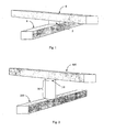
- Fig. 1 is a perspective view of a possible memory cell having a resistance-switching material disposed between conductors.
- Fig. 2 is a perspective view of a rewriteable nonvolatile memory cell formed according to the present invention.
- Fig. 3 is a perspective view of a memory level comprising cells like those shown in Fig. 2 .
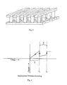
- Fig. 4 is an I-V curve showing the low-to-high and high-to-low resistance conversions of nondirectional resistance-switching material.
- Fig. 5a is an I-V curve showing the low-to-high resistance conversion of directional resistance-switching material.
- Fig. 5b is an I-V curve showing the high-to-low resistance conversion of directional resistance-switching material.
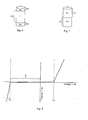
- Fig. 6 is a perspective view of a vertically oriented p-i-n diode preferred in some embodiments of the present invention.
- Fig. 7 is a perspective view of a vertically oriented Zener diode preferred in other embodiments of the present invention.
- Fig. 8 is an I-V curve of a p-i-n diode like the diode of Fig. 6 .
- Fig. 9 is an I-V curve of a Zener diode like the diode of Fig 7 .
- Fig. 10 is a perspective view of an embodiment of the present invention in which the resistance-switching material is sandwiched between noble metal layers.
- Fig. 11a is a cross-sectional view illustrating an embodiment of the present invention in which the resistance-switching material is not patterned and etched.
- Fig. 11b is a perspective view of a preferred embodiment of the present invention in which the resistance-switching material is patterned and etched with the top conductor.
- Fig. 12 is a graph depicting current vs. voltage for four different data states of a memory cell in an embodiment of the present invention.
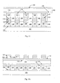
- Figs 13a-13c are cross-sectional views illustrating stages in the formation of a memory level of a monolithic three dimensional memory array formed according to a preferred embodiment of the present invention.
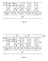
- Fig. 14 is a cross-sectional view illustrating a portion of a monolithic three dimensional memory array formed according to a preferred embodiment of the present invention.
- Fig. 15 is a cross-sectional view illustrating a portion of a monolithic three dimensional memory array formed according to a different preferred embodiment of the present invention.
- Figs. 16a-16c are cross-sectional views illustrating stages in formation of a memory level of a monolithic three dimensional memory array formed according to yet another preferred embodiment of the present invention.
- a variety of materials show reversible resistivity-switching behavior. These materials include chalcogenides, carbon polymers, perovskites, and certain metal oxides and nitrides. Specifically, there are metal oxides and nitrides which include only one metal and exhibit reliable resistivity switching behavior, as described by Pagnia and Sotnick in "Bistable Switching in Electroformed Metal-Insulator-Metal Device," Phys. Stat. Sol. (A) 108, 11-65 (1988 ).
- This group includes, for example, Ni x O y , Nb x O y , Ti x O y , Hf x O y , Al x O y , Mg x O y , Co x O y , Cr x O y , V x O y , Zn x O y , Zr x O y , B x N y , and Al x N y , where x and y range between 0 and 1.
- Examples are the stoichiometric compounds NiO, Nb 2 O 5 , TiO 2 , HfO 2 , Al 2 O 3 , MgO, CoO, CrO 2 , VO, ZnO, ZrO, BN, and AlN, but nonstoichiometric compounds may be used as well.
- a layer of one of these materials may be formed in an initial state, for example a relatively low-resistivity state. Upon application of sufficient voltage, the material switches to a stable high-resistivity state. This resistivity switching is reversible; subsequent application of appropriate current or voltage can serve to return the resistivity-switching material to a stable low-resistivity state. This conversion can be repeated many times.
- the initial state is high-resistivity rather than low-resistance.
- resistivity-switching material resistivity-switching metal oxide or nitride
- resistivity-switching memory element resistivity-switching memory element
- resistivity-switching materials thus are of interest for use in nonvolatile memory arrays.
- One resistivity state may correspond to a data "0", for example, while another resistivity state corresponds to a data "1".
- Some of these materials may have more than two stable resistivity states; indeed some may be able to achieve any of a plurality of data states.
- the difference in resistivity between the high-resistivity state and the low-resistivity state must be large enough to be readily detectable.
- the resistivity of the material in the high-resistivity state should be at least three times that of the material in the low-resistivity state.
- a plurality of memory cells are formed, each as shown in Fig. 1 , comprising a resistance-switching memory element 2 (comprising one of the resistivity-switching materials named), disposed between conductors, for example between a top conductor 4 and a bottom conductor 6, in a cross-point array.
- a resistance-switching memory element 2 is programmed by applying voltage between the top conductor 4 and bottom conductor 6.
- a diode is paired with a resistivity-switching material to form a rewriteable nonvolatile memory cell that can be formed and programmed in a large, high-density array. Using the methods described herein, such an array can be reliably fabricated and programmed.
- the cell includes a bottom conductor 200 comprising conductive material, for example heavily doped semiconductor material, conductive silicides, or preferably a metal, for example tungsten, aluminum, or copper.
- a top conductor 400 which may be of the same material as the bottom conductor.
- the rail-shaped top and bottom conductors preferably extend in different directions; for example they may be perpendicular.
- the conductors may include conductive barrier or adhesion layers as required.
- a diode 30 and a resistance-switching element 118 Disposed between the top conductor 400 and bottom conductor 200 are a diode 30 and a resistance-switching element 118 arranged in series. Other layers, for example barrier layers, may also be included between conductors 200 and 400.
- the resistance-switching element 118 is converted from the low-resistance state to the high-resistance state, or, alternatively, from the high-resistance state to the low-resistance state, upon application of voltage across or flow of current through the resistance-switching element 118. The conversion from low resistance to high resistance is reversible.
- the diode 30 acts as a one-way valve, conducting current more easily in one direction than in the other. Below a critical "turn-on" voltage in the forward direction, the diode 30 conducts little or no current.
- the diodes of neighboring cells can serve to electrically isolate the resistance-switching elements of those cells and thus prevent inadvertent programming, so long as the voltage across unselected or half-selected cells does not exceed the turn-on voltage of the diode when applied in the forward direction, or the reverse breakdown voltage when applied in the reverse direction.
- a plurality of such top and bottom conductors, with intervening diodes and resistance-switching elements, can be fabricated, forming a first memory level, a portion of which is shown in Fig. 3 .
- additional memory levels can be formed stacked above this first memory level, forming a highly dense monolithic three dimensional memory array.
- the memory array is formed of deposited and grown layers above a substrate, for example a monocrystalline silicon substrate. Support circuitry is advantageously formed in the substrate below the memory array.
- Preferred embodiments include several important variations. In general, the properties of the resistivity-switching material selected, and the manner in which the memory cell is intended to be used, will determine which embodiments are most advantageous.
- Nondirectional vs. Directional Switching In general, the resistance-switching metal oxides and nitrides named earlier exhibit one of two general kinds of switching behavior. Referring to the I-V curve of Fig. 4 , some of these materials are initially in a low-resistivity state, in area A on the graph. Current flows readily for applied voltage until a first voltage V 1 is reached. At voltage V 1 the resistivity-switching material converts to a high-resistivity state, shown in area B, and reduced current flows. At a certain critical higher voltage V 2 , the material switches back to the initial low-resistivity state, and increased current flows. Arrows indicate the order of state changes. This conversion is repeatable. For these materials, the direction of current flow and of voltage bias is immaterial; thus these materials will be referred to as nondirectional. Voltage V 1 may be called the reset voltage while voltage V 2 may be called the set voltage.
- Figs. 5a and 5b Others of the resistivity-switching materials, on the other hand, behave as shown in Figs. 5a and 5b , and will be called directional.
- Directional resistivity-switching materials may also be formed in a low-resistance state, shown in area A of Fig. 5a .
- V 1 the directional resistivity-switching material converts to a high-resistivity state, shown in area B in Fig. 5a .
- a reverse voltage must be applied. As shown in Fig.
- the directional resistivity-switching material is high-resistance in area B at negative voltage until a critical reverse voltage V 2 , the set voltage. At this voltage the directional resistivity-switching material reverts to the low-resistivity state. Arrows indicate the order of state changes. (Some materials are initially formed in a high-resistivity state. The switching behavior is the same; for simplicity only one initial state has been described.)
- nondirectional resistivity-switching materials may be paired with a substantially one-directional diode.
- One such diode is a p-i-n diode, shown in Fig. 6 .
- a preferred p-i-n diode is formed of semiconductor material, for example silicon, and includes a bottom heavily doped region 12 having a first conductivity type, a middle intrinsic region 14 which is not intentionally doped, and a top heavily doped region 16 having a second conductivity type opposite the first.
- bottom region 12 is n-type while top region 16 is p-type; if desired the polarity can be reversed.
- a diode behaves as shown by the I-V curve of Fig. 8 . Little or no current flows at very low voltage.
- V 3 the turn-on voltage of the diode, the diode begins to conduct and significant forward current flows.
- the diode acts as a one-way valve.
- Directional resistivity-switching materials thus may not advantageously be paired with a one-way diode. Instead such materials may be paired with a reversible non-ohmic device, i.e. one that allows current flow in either direction.
- a Zener diode is shown in Fig. 7 . It will be seen that such a diode has a first heavily doped region 12 of a first conductivity type and a second heavily doped region 16 of the opposite conductivity type. The polarity could be reversed.
- Fig. 7 There is no intrinsic region in the Zener diode of Fig. 7 ; in some embodiments there may be a very thin intrinsic region.
- Zener diode 9 shows an I-V curve of a Zener diode.
- the Zener diode behaves like a p-i-n diode under forward bias, with turn-on voltage V 3 . Under reverse bias, however, once a critical voltage V 4 is reached, the Zener diode will allow a reverse current to flow. In a Zener diode the critical reverse voltage V 4 is substantially lower in magnitude than that of a one-way diode.
- Such a controllable reverse current at moderate voltage is required to convert directional resistivity-switching material from the high-resistivity to the low-resistivity state, as described earlier and shown in Fig. 5b (at voltage V 2 ).
- a Zener diode is preferred.
- a p-i-n diode having a very small intrinsic region and a Zener diode is artificial, but is made routinely by those skilled in the art.
- Nondirectional materials don't require current in both the forward and the reverse direction, but, as described, resistivity-switching can be achieved in either direction. For some circuit arrangements, then, it may be advantageous to pair a nondirectional resistivity-switching material with a Zener diode.
- junction diode is used herein to refer to a semiconductor device with the property of non-ohmic conduction, having two terminal electrodes, and made of semiconducting material which is p-type at one electrode and n-type at the other.
- Examples include p-n diodes and n-p diodes, which have p-type semiconductor material and n-type semiconductor material in contact, such as Zener diodes, and p-i-n diodes, in which intrinsic (undoped) semiconductor material is interposed between p-type semiconductor material and n-type semiconductor material.
- the diode To reset the resistivity-switching material, causing the transition from the high-resistivity to the low-resistivity state in nondirectional resistivity-switching materials, for some materials a relatively high current may be required. For these materials, it may be preferred for the diode to be germanium or a germanium alloy, which provides higher current at a given voltage compared to silicon.
- noble metal layer 117 is adjacent to semiconductor diode 30. Extensive diffusion of a noble metal into the semiconductor material of diode 30 will damage device performance. When the resistivity-switching element is formed between noble metal contacts, then, it is advantageous to minimize processing temperatures.
- the diode may be silicon, germanium, or a silicon-germanium alloy. Germanium can be crystallized at lower temperatures than silicon, and as the germanium content of a silicon-germanium alloy increases, the crystallization temperature decreases. Diodes formed of germanium or germanium alloys may be preferred when noble metal contacts are used.
- polycrystalline silicon in this discussion polycrystalline silicon will be referred to as polysilicon while polycrystalline germanium will be referred to as polygermanium
- polysilicon diodes incompatible with certain metals having relatively low melting points.
- aluminum wires begin to soften and extrude when exposed to temperatures above about 475 degrees C.
- tungsten wiring it is preferred to use tungsten in the conductors, as tungsten wiring can withstand higher temperatures.
- germanium or a germanium alloy is used, however, the lower deposition and crystallization temperatures of germanium may allow the use of aluminum or even copper in the conductors, for example in conductors 200 and 400 of Fig 10 . These metals have low sheet resistance, and thus are generally preferable if the thermal budget allows their use, though tungsten or some other conductive material may be used instead.
- Conductivity and Isolation It has been described that to enable programming in large arrays, a diode is included in each memory cell to provide electrical isolation between neighboring cells. Some resistivity-switching materials are deposited in a high-resistivity state, while others are deposited in a low-resistivity state. For a resistivity-switching material deposited in a high-resistivity state, in general, conversion to a low-resistivity state is a localized phenomenon. For example, referring to Fig.
- a memory cell (shown in cross-section) includes a rail-shaped bottom conductor 200, extending left to right across the page, a diode 30, a layer 118 of resistivity-switching material formed in a high-resistivity state, and a rail-shaped top conductor 400 extending out of the page.
- the layer 118 of resistivity-switching material has been formed as a blanket layer. So long as the high-resistivity state of the layer 118 of resistivity-switching material is sufficiently high, layer 118 will not provide an undesired conductive path, shorting conductor 400 to adjacent conductors or diode 30 to adjacent diodes.
- layer 118 of resistivity-switching material When layer 118 of resistivity-switching material is exposed to a high voltage and is converted to a low-resistivity state, it is expected that only the areas of layer 118 immediately adjacent to the diode will be converted; for example, after programming, the shaded region of layer 118 will be low-resistivity, while the unshaded region will remain high-resistivity.
- the shaded regions are resistivity-switching elements disposed within a continuous layer 118 of resistivity-switching material.
- the high-resistivity state of the resistivity-switching material may be too conductive for reliable isolation, and will tend to short adjacent conductors or diodes when formed in a continuous layer as in Fig. 11a .
- a memory element When a memory element is formed of a resistivity-switching material which is formed in a low-resistivity state, it must be isolated from the resistivity-switching memory element of adjacent cells to avoid forming an unwanted conductive path between them.
- both the polysilicon of diode 30 and the resistivity-switching element 118 Upon first application of a programming voltage, both the polysilicon of diode 30 and the resistivity-switching element 118 will be converted to their low-resistivity states. In general the conversion of the diode 30 is permanent, while the conversion of resistivity-switching element 118 is reversible. It may be desirable to perform the initial conversion of the polysilicon of the diodes from high-resistivity to low-resistivity in factory conditions, effectively "preconditioning" the diode.
- the silicide layer provides an orderly crystallization template for the silicon as it crystallizes, resulting in a highly crystalline diode as formed, with fewer crystalline defects.
- This technique could be used in the present invention.
- the diode is germanium
- a germanium diode is crystallized adjacent to a germanide layer, such as TiGe 2 , which will provide an analogous crystallization template for the germanium.
- the germanium of such a diode will be a low-resistivity as formed, with no need for a "programming" step to create a low-resistance path through it.
- a diode paired with a resistance-switching element has been described in embodiments of the present invention when used as a rewriteable memory cell. These elements can also be used in alternative embodiments to form a one-time-programmable memory cell.
- nickel oxide or any of the named resistivity-switching binary metal oxides or nitrides, which can switch between lower- and higher-resistivity states
- the reset switch from a lower-resistivity to a higher-resistivity state
- nickel oxide may refer either to stoichiometric NiO or to a nonstoichiometric compound.
- the actual switch mechanism is unclear, it appears that a certain voltage must be applied across the resistivity-switching layer to cause it to switch. If the set state of the material is very low-resistivity, and the material is highly conductive, it can be difficult to build sufficient voltage to cause the switch to take place.
- the memory cell of the present invention as a one-time programmable cell, the more difficult switch can be avoided. This generally simplifies programming circuitry.
- nickel oxide is nondirectional, meaning that the material alone switches with either positive or negative voltage applied.
- Resetting of a nickel oxide layer is most readily achieved with the diode under reverse bias.
- Extra transistors may be required in the substrate to provide negative voltage to reverse bias the diodes. These transistors consume substrate space, making the device more expensive, and forming these transistors may add process complexity.
- reverse bias is required for reset, using the cell as a write-once cell and avoiding reset avoids the difficulties of generating negative voltage.
- a memory cell comprising a diode and a resistivity-switching layer according to the present invention as a one-time programmable memory cell
- the cell has two values, unprogrammed and programmed, which correspond to two distinct read currents through the cell.
- the set voltage will vary depending on the material used for the resistance-switching element, the thickness of the layer, characteristics of the material, and other factors. Increasing the pulse time may reduce the voltage required to set the material from high-resistance to low-resistance.
- the set voltage may vary from, for example, 4 volts to 10 volts.
- the diode is formed of polysilicon
- crystallizing the polysilicon adjacent to a silicide having a lattice structure at an orientation which provides a good crystallization template for silicon will result in lower-defect, lower-resistivity polysilicon; while crystallizing adjacent only to materials having a poor lattice match, such as titanium nitride, will result in higher-defect, higher-resistivity polysilicon.
- the diode is formed of more highly resistive polysilicon, application of a suitable programming voltage across a diode is required to convert the polysilicon to a low-resistivity state, leaving the diode with good rectifying behavior.
- a forming pulse may be required to achieve the first switch from high to low resistivity.
- This forming pulse may require a higher voltage than subsequent low-to-high or high-to-low-resistivity switches.
- the forming pulse was about 8.5-9 volts, while subsequent set pulses were about 6.5-7 volts.
- adding a metal to the binary metal oxide or nitride can decrease set and reset voltages, and may decrease the amplitude of the forming pulse or eliminate the need for one entirely.
- the metal additive is between about 0.01 and about 5 percent of the metal atoms in the layer of metal oxide or nitride compound.
- Preferred metals to use for the metal additive are selected from the group consisting of cobalt, aluminum, gallium, indium, manganese, nickel, niobium, zirconium, titanium, hafnium, tantalum, magnesium, chromium, vanadium, boron, yttrium, and lanthanum.
- a one-time-programmable memory cell including a binary metal oxide or nitride resistance-switching element and a diode.
- the effect of pairing the resistance-switching element with a diode of high- or low-resistivity polysilicon should be considered.
- the binary metal oxide or nitride is formed in a high-resistivity state and the diode is formed of low-defect, low-resistivity polysilicon
- conversion of the memory cell to a programmed state, in which high current flows under a read voltage is achieved by converting the binary metal oxide or nitride to the set state.
- the diode is formed of high-defect, high-resistivity polysilicon, however, the polysilicon of the diode must also undergo a programming voltage for the memory cell to behave as if programmed, allowing high current flow under applied read voltage.
- the polysilicon crystallized adjacent to an appropriate silicide may be preferred.
- a large forming pulse is required for binary metal oxide or nitride formed in a high-resistivity state, is to apply the forming pulse in a preconditioning step in the factory.
- the high voltage required for the forming pulse can be supplied from outside of the die, and thus need not be available on the die.
- the reset pulse can also be applied in a further preconditioning step, so when the memory array is ready for the end user, the cells are in the reset state, and can be programmed by the lower, post-forming set voltage. In this way circuits on the die do not need to provide either the high-voltage forming pulse or negative voltage, simplifying circuit requirements.
- the large voltage required for a forming pulse may be sufficient to convert high-defect polysilicon of the diode from high-resistivity to low-resistivity.
- Such a memory cell in a memory array (wherein the memory cell comprises a resistivity-switching layer of a metal oxide or nitride compound, the metal oxide or nitride compound including exactly one metal), is programmed by a method comprising: programming the memory cell by changing the resistivity-switching layer from a first resistivity state to a second programmed resistivity state, wherein the second programmed resistivity state stores a data state of the memory cell.
- the memory array comprises circuitry to program and read the memory cell, and the circuitry is adapted to program the memory cell no more than one time.
- the memory array is a one-time-programmable array.
- the binary metal oxide or nitride with a diode formed of high-defect polysilicon.
- the two states of the polysilicon making up the diode, the initial high-resistivity state and the programmed low-resistivity state, can be used to store data, increasing the density of the memory cell.
- the diode For example, suppose a diode formed of high-defect polysilicon (not crystallized adjacent to an appropriate silicide) is paired with a layer of nickel oxide, the two arranged electrically in series between top and bottom conductors.
- the nickel oxide is formed in a high-resistivity state, requiring a forming pulse to effect the first conversion from high-resistivity to low-resistivity.
- the diode requires a programming voltage of 8 volts to cause the disorder-to-order conversion described in the '530 application, converting the polysilicon to a higher-resistivity state.
- the voltage required by the nickel oxide for the forming pulse is 10 volts. (It will be understood the voltages given here are examples only. Voltages will change as device characteristics and other factors are varied.)
- the memory cell as formed has high-resistivity nickel oxide and a diode of high-resistivity polysilicon.
- Table 1 summarizes three data states that may be achieved by this memory cell. It also includes, for this example, the programming required to attain each state, and example read current to be expected for each data state at an applied read voltage of +2 volts: Table 1 Data State Polysilicon State Switching Layer State Programming Read current at +2 V 00 High-resistivity Reset No programming 1 x 10 -10 amps 10 Low-resistivity Reset +8 V 1 x 10 -8 amps 11 Low-resistivity Set +11 V 1 x 10 -5 amps
- the memory cell as formed is in a first data state, which for convenience will be called the '00' state.
- Application of +8 volts is sufficient to convert the polysilicon of the diode from high-resistivity to low-resistivity, but is below the voltage required for the forming pulse, leaving the nickel oxide in its initial, high-resistivity state; this data state will be called '10'.
- Application of +11 volts to a cell in the initial '00' state is sufficient both to effect the disorder-to-order conversion of the polysilicon and to set the nickel oxide to a low-resistivity state. This data state will be called the '11' state.
- no forming pulse, or only a small forming pulse may be required, and the set voltage may be less than the voltage required to switch the polysilicon.
- Table 2 Data State Polysilicon State Switching Layer S tate Programming Read current at +2 V 00 High-resistivity Reset No programming 1 x 10 -10 amps 01 High-resistivity Set +6 V 1 x 10 -9 amps 11 Low-resistivity Set +8 V 1 x 10 -5 amps
- the memory cell is in the '00' state, with both polysilicon and nickel oxide high-resistivity. Applying +6 volts sets the nickel oxide, but is not sufficient to switch the polysilicon, leaving the cell in the '01' state. Applying 8 volts switches both the polysilicon and the nickel oxide, leaving both in the low-resistivity states, corresponding to the '11' data state.
- a fourth data state in which the polysilicon of the diode is in the low-resistivity state and the nickel oxide is in the reset state, can be achieved by resetting the nickel oxide.
- This state will be called the '10' state, and, in embodiments in which reverse bias is required for reset, is achieved by applying a negative reset pulse, say -4 volts to a cell in the '11' state.
- the memory cell just described is programmed by a method comprising i) applying a first programming pulse to the memory cell wherein the first programming pulse: a) detectably changes a first resistivity state of the resistivity-switching layer; or b) detectably changes a second resistivity state of the polycrystalline semiconductor material, or c) detectably changes the first resistivity state of the resistivity-switching layer and detectably changes the second resistivity state of the polycrystalline semiconductor material; and ii) reading the memory cell, wherein the first resistivity state of the resistivity switching layer serves to store data and the second resistivity state of the polycrystalline semiconductor material serves to store data.
- the memory cell is adapted to store one of three or four data states.
- resistivity-switching binary oxides or nitrides mentioned herein are capable of attaining more than just two stable resistivity states.
- memory cells of an array formed according to the present invention are capable of storing more than two data states, for example three, four, or more data states, by putting the metal oxide or nitride in one of three, four, or more detectably distinct resistivity states. Detectably distinct data states can reliably be detected by sensing and decoding circuitry in the array. These embodiments can be either rewriteable or one-time-programmable.
- the resistivity-switching metal oxide or nitride is nickel oxide (it will be understood that any of the other named materials may be used), which has been formed in a high-resistivity state.
- the nickel oxide is in the lowest-resistivity state, shown on the curve labeled 00.
- the nickel oxide may be put into more than two detectably distinct resistivity states.
- a memory cell like the one shown in Fig. 2 may have four different states, each distinguished by a range of current flow under an applied read voltage, for example about 2 volts.
- the '00' state In this example, in the highest-resistivity state, less than about 30 nanoamps of current flows when 2 volts is applied across the memory cell; this will be called the '00' state. In the '01' state, at 2 volts, the current will be between about 100 and 300 nanoamps. In the '10' state, at 2 volts, the current will be between about 1 microamp and 3 microamps. In the lowest-resistivity state, the '11' state, the current at 2 volts will be more than 9 microamps. It will be understood that these current ranges and read voltage are supplied for clarity only; depending on the actual materials used and the characteristics of the device, other values may be appropriate.
- a set pulse has a voltage between about 8 and about 10 volts, while a reset voltage is between about 3 and about 6 volts.
- the reset voltage is applied in reverse bias. Depending on the material used and the configuration and characteristics of the memory cell, though, reverse bias may not be required to reset the cell.
- the cell is formed in the '00' state.
- a set voltage of, for example, 8 volts may be applied.
- a current limiter is preferably included in the circuit.
- the cell is read at 2 volts. If the current at 2 volts is in the expected range for the '01' state, between about 100 and about 300 nanoamps, the cell is considered to be programmed. If the current is too low, (80 nanoamps, for example) an additional set pulse, optionally at a higher set voltage, is applied, and the cell is read again at 2 volts. The process is repeated until the current through the memory cell is within the correct range at 2 volts.
- the current may instead be above the acceptable range for the '01' state; it may be 400 nanoamps, for example.
- a reset pulse sufficient to return the nickel oxide to the '00' state can be applied, followed by another, possibly smaller, set pulse; or a reset pulse can be applied to increase the resistivity of the nickel oxide layer slightly, moving it incrementally into the '01' range. The process is repeated until the current through the memory cell is within the correct range at 2 volts.
- a similar approach is taken to place the memory cell in the '10' or '11' states. For example, a set voltage of 9.5 volts may be sufficient to place the memory cell in the '10' state, while a set voltage of 10 volts may program the memory cell to the '11' data state.
- the memory cell is preferably used as a rewriteable memory cell. However, it may be preferable, to save space in the substrate, to omit transistors capable of applying reverse bias, and only program the cell under forward bias. If reverse bias is not required to reset the cell, such a memory array may be rewriteable. If reverse bias is required for reset, however, such a memory array could be used as a one-time programmable array. In this case great care must be taken never to set the cell to a state with higher current (lower resistivity of the nickel oxide layer) than desired for the intended data state. Deliberately low set voltages can be applied to lower the resistivity of the nickel oxide layer gradually and raise the current into the acceptable range, avoiding ever topping the desired range, since in this case, with no reverse bias, this overshoot could not be corrected.
- the advantages or disadvantages of forming a diode of low-defect polysilicon by crystallizing the polysilicon adjacent to an appropriate silicide should be considered. If a high-amplitude forming pulse is required, the voltage of the forming pulse may be sufficient to convert high-defect, high-resistivity polysilicon to lower-resistivity polysilicon; in this case the use of low-defect, silicided polysilicon may afford no advantage. If no forming pulse or a small forming pulse is required, a diode formed of low-defect, low-resistivity polysilicon, crystallized adjacent to an appropriate silicide, may be preferred.
- a preconditioning step such as a forming pulse, must be applied, it may be advantageous to perform this step in the factory. In this case the high voltage need not be present on the die.
- a detailed example will be provided of fabrication of a monolithic three dimensional memory array formed according to a preferred embodiment of the present invention. For clarity many details, including steps, materials, and process conditions, will be included. It will be understood that this example is non-limiting, and that these details can be modified, omitted, or augmented while the results fall within the scope of the invention.
- the '470 application, the '549 application, the '824 application, and the '577 application teach memory arrays comprising memory cells, wherein each memory cell is a one-time programmable cell.
- the cell is formed in a high-resistance state, and, upon application of a programming voltage, is permanently converted to a low-resistance state.
- teachings of the '470, '549, '824, '577 and other incorporated applications and patents may be relevant to formation of a memory according to the present invention. For simplicity, not all of the details of the incorporated applications and patents will be included, but it will be understood that no teaching of these applications or patents is intended to be excluded.
- This substrate 100 can be any semiconducting substrate as known in the art, such as monocrystalline silicon, IV-IV compounds like silicon-germanium or silicon-germanium-carbon, III-V compounds, II-VII compounds, epitaxial layers over such substrates, or any other semiconducting material.
- the substrate may include integrated circuits fabricated therein.
- the insulating layer 102 is formed over substrate 100.
- the insulating layer 102 can be silicon oxide, silicon nitride, high-dielectric film, Si-C-O-H film, or any other suitable insulating material.
- the first conductors 200 are formed over the substrate 100 and insulator 102.
- An adhesion layer 104 may be included between the insulating layer 102 and the conducting layer 106 to help the conducting layer 106 adhere.
- a preferred material for the adhesion layer 104 is titanium nitride, though other materials may be used, or this layer may be omitted.
- Adhesion layer 104 can be deposited by any conventional method, for example by sputtering.
- the thickness of adhesion layer 104 can range from about 20 to about 500 angstroms, and is preferably between about 100 and about 400 angstroms, most preferably about 200 angstroms. Note that in this discussion, "thickness” will denote vertical thickness, measured in a direction perpendicular to substrate 100.
- conducting layer 106 can comprise any conducting material known in the art, such as doped semiconductor, metals such as tungsten, or conductive metal silicides; in a preferred embodiment, conducting layer 106 is aluminum.
- the thickness of conducting layer 106 can depend, in part, on the desired sheet resistance and therefore can be any thickness that provides the desired sheet resistance. In one embodiment, the thickness of conducting layer 106 can range from about 500 to about 3000 angstroms, preferably about 1000 to about 2000 angstroms, most preferably about 1200 angstroms.
- Another layer 110 preferably of titanium nitride, is deposited on conducting layer 106. It may have thickness comparable to that of layer 104. A photolithography step will be performed to pattern aluminum layer 106 and titanium nitride layer 104. The high reflectivity of aluminum makes it difficult to successfully perform photolithography directly on an aluminum layer. Titanium nitride layer 110 serves as an anti-reflective coating.
- the layers will be patterned and etched using any suitable masking and etching process to form substantially parallel, substantially coplanar conductors 200, shown in Fig. 13a in cross-section.
- photoresist is deposited, patterned by photolithography and the layers etched, and then the photoresist removed, using standard process techniques such as "ashing" in an oxygen-containing plasma, and strip of remaining polymers formed during etch in a conventional liquid solvent such as those formulated by EKC.
- Dielectric material 108 is deposited over and between conductor rails 200.
- Dielectric material 108 can be any known electrically insulating material, such as silicon oxide, silicon nitride, or silicon oxynitride.
- silicon oxide is used as dielectric material 108.
- the silicon oxide can be deposited using any known process, such as chemical vapor deposition (CVD), or, for example, high-density plasma CVD (HDPCVD).
- bottom conductors 200 are formed by depositing a first layer or stack of conductive material; patterning and etching the first layer or stack of conductive material to form first conductors; and depositing dielectric fill between the first conductors.
- conductor rails can be formed by a damascene process, in which oxide is deposited, trenches are etched in the oxide, then the trenches are filled with conductive material to create the conductor rails. Formation of conductors 200 using a copper damascene process is described in Herner et al., US Patent Application No. No. 11/125,606 , "High-Density Nonvolatile Memory Array Fabricated at Low Temperature Comprising Semiconductor Diodes.” Copper damascene conductors include at least a barrier layer and a copper layer.
- semiconductor material that will be patterned into pillars is deposited
- the semiconductor material can be germanium, silicon, silicon-germanium, silicon-germanium-carbon, or other suitable IV-IV compounds, gallium arsenide, indium phosphide, or other suitable III-V compounds, zinc selinide, or other II-VII compounds, or a combination.
- Silicon-germanium alloys of any proportion of silicon and germanium, for example including at least 20, at least 50, at least 80, or at least 90 atomic percent germanium or pure germanium may be used. The present example will describe the use of pure germanium.
- the term "pure germanium” does not exclude the presence of conductivity-enhancing dopants or contaminants normally found in a typical production environment.
- the semiconductor pillar comprises a junction diode, the junction diode comprising a bottom heavily doped region of a first conductivity type and a top heavily doped region of a second conductivity type.
- the middle region, between the top and bottom regions, is an intrinsic or lightly doped region of either the first or second conductivity type.
- bottom heavily doped region 112 is heavily doped n-type germanium.
- heavily doped region 112 is deposited and doped with an n-type dopant such as phosphorus by any conventional method, preferably by in situ doping. This layer is preferably between about 200 and about 800 angstroms.
- the germanium that will form the remainder of the diode is deposited.
- a subsequent planarization step will remove some germanium, so an extra thickness is deposited. If the planarization step is performed using a conventional CMP method, about 800 angstroms of thickness may be lost (this is an average; the amount varies across the wafer. Depending on the slurry and methods used during CMP, the germanium loss may be more or less.) If the planarization step is performed by an etchback method, only about 400 angstroms of germanium or less may be removed.
- between about 800 and about 4000 angstroms of undoped germanium is deposited by any conventional method; preferably between about 1500 and about 2500 angstroms; most preferably between about 180.0. and about 2200 angstroms.
- the germanium can be lightly doped. Top heavily doped region 116 will be formed in a later implant step, but does not exist yet at this point, and thus is not shown in Fig. 13b .
- Pillars 300 should have about the same pitch and about the same width as conductors 200 below, such that each pillar 300 is formed on top of a conductor 200. Some misalignment can be tolerated.
- the pillars 300 can be formed using any suitable masking and etching process.
- photoresist can be deposited, patterned using standard photolithography techniques, and etched, then the photoresist removed.
- a hard mask of some other material for example silicon dioxide, can be formed on top of the semiconductor layer stack, with bottom antireflective coating (BARC) on top, then patterned and etched.
- BARC bottom antireflective coating
- DARC dielectric antireflective coating
- Dielectric material 108 is deposited over and between pillars 300, filling the gaps between them.
- Dielectric material 108 can be any known electrically insulating material, such as silicon oxide, silicon nitride, or silicon oxynitride.
- silicon dioxide is used as the insulating material.
- the silicon dioxide can be deposited using any known process, such as CVD or HDPCVD.
- the dielectric material on top of the pillars 300 is removed, exposing the tops of pillars 300 separated by dielectric material 108, and leaving a substantially planar surface.
- This removal of dielectric overfull and planarization can be performed by any process known in the art, such as CMP or etchback.
- CMP chemical vapor deposition
- etchback the etchback techniques described in the '417 application by Raghuram et al. can be used.
- the resulting structure is shown in Fig. 13b .
- heavily doped top regions 116 are formed at this point by ion implantation with a p-type dopant, for example boron or BF 2 .
- a p-type dopant for example boron or BF 2 .
- the diode described herein has a bottom n-type region and a top p-type region. If preferred, the conductivity types could be reversed. If desired, p-i-n diodes having an n-region on the bottom could be used in one memory level while p-i-n diodes having a p-type region on the bottom could be used in another memory level.
- the diodes that reside in pillars 300 were formed by a method comprising depositing a semiconductor layer stack above the first conductors and dielectric fill; and patterning and etching the semiconductor layer stack to form the first diodes.
- a layer 121 of a conductive barrier material for example titanium nitride, a metal, or some other appropriate material, is deposited.
- the thickness of layer 121 may be between about 100 and about 400 angstroms, preferably about 200 angstroms. In some embodiments, layer 121 may be omitted.
- a layer 118 of a metal oxide or nitride resistance-switching material is deposited on barrier layer 121. This layer is preferably between about 50 and about 400 angstroms, for example between about 100 and about 200 angstroms.
- Layer 118 can be any of the materials described earlier, and is preferably formed of a metal oxide or nitride having including exactly one metal which exhibits resistance switching behavior; preferably a material selected from the group consisting of Ni x O y , Nb x O y , Ti x O y , Hf x O y , Al x O y , Mg x O y , Co x O y , Cr x O y , V x O y , Zn x O y , Zr x O y , B x N y , and Al x N y .
- Ni x O y , Nb x O y Ti x O y , Hf x O y , Al x O y , Mg x O y , Co x O y , Cr x O y , V x O y , Zn x O y , Zr x O y
- nickel oxide exhibits nondirectional switching behavior, and thus has been paired with a p-i-n diode, though a Zener diode could have been used had the circuit arrangement dictated such a choice. As described earlier, had a directional resistance switching material been selected, a Zener diode would have been preferred. In a preferred embodiment, such a Zener diode has no intrinisic region, or has an intrinsic region no thicker than about 350 angstroms.
- barrier layer 123 is deposited on nickel oxide layer 118.
- Layer 123 is preferably titanium nitride, though some other appropriate conductive barrier material may be used instead.
- the purpose of barrier layer 123 is to allow an upcoming planarization step to be performed on barrier layer 123 rather than nickel oxide layer 118. In some embodiments, layer 123 may be omitted.
- Layers 123, 118, and 121 are patterned and etched to form short pillars, ideally directly on top of pillars 300 formed in the previous pattern and etch step. Some misalignment may occur, as shown in Fig. 13c , and can be tolerated.
- the photomask used to pattern pillars 300 may be reused in this patterning step.
- layers 123, 118, and 121 were patterned in a different patterning step than germanium layers 112 and 114 (and 116, formed in a subsequent ion implantation step.) This may be desirable in order to reduce etch height and to avoid possible contamination by having nickel oxide and metal barrier layers exposed in a chamber devoted to semiconductor etch. In other embodiments, however, it may be preferred to pattern layers 123, 118, 121, 116, 114, and 112 in a single patterning step. In this case the ion implantation of heavily doped germanium layer 116 takes place before the deposition of barrier layer 121. Alternatively, heavily doped layer 116 may be in situ doped.
- barrier layer 121, nickel oxide layer 118, and barrier layer 123 can be formed before (and therefore beneath) diode layers 112, 114, and 116, and may be patterned in the same or in a separate patterning step.
- top conductors 400 a conductive material or stack is deposited to form the top conductors 400.
- titanium nitride barrier layer 120 is deposited next, followed by aluminum layer 122 and top titanium nitride barrier layer 124.
- Top conductors 400 can be patterned and etched as described earlier. In this example in each cell the diode (of layers 112, 114, and 116) and a resistance-switching element (a portion of nickel oxide layer 118) have been formed in series between top conductor 400 and bottom conductor 200. Overlying second conductors 400 will preferably extend in a different direction from first conductors 200, preferably substantially perpendicular to them.
- the resulting structure, shown in Fig. 13c is a bottom or first story of memory cells.
- top conductors can comprise copper, and can be formed by a damascene method.
- a detailed description of fabrication of top copper conductors in a monolithic three dimensional memory array is provided in detail in Herner et al., US Patent Application No. No. 11/125,606 , "High-Density Nonvolatile Memory Array Fabricated at Low Temperature Comprising Semiconductor Diodes.”
- this first story of memory cells is a plurality of nonvolatile memory cells comprising: a first plurality of substantially parallel, substantially coplanar conductors extending in a first direction; a first plurality of diodes; a first plurality of reversible resistance-switching elements; and a second plurality of substantially parallel, substantially coplanar conductors extending in a second direction different from the first direction, wherein, in each memory cell, one of the first diodes and one of the first reversible resistance-switching elements are arranged in series, disposed between one of the first conductors and one of the second conductors, and wherein the first plurality of reversible resistance-switching elements comprise a material selected from the group consisting of Ni x O y , Nb x O y , Ti x O y , Hf x O y , Al x O y , Mg x O y , Co x O y , Cr x O
- Additional memory levels can be formed above this first memory level.
- conductors can be shared between memory levels; i.e. top conductor 400 would serve as the bottom conductor of the next memory level.
- an interlevel dielectric is formed above the first memory level of Fig. 13c , its surface planarized, and construction of a second memory level begins on this planarized interlevel dielectric, with no shared conductors. If top conductors 400 are not shared between memory levels, then no CMP step need be performed on these conductors. In this case, if desired, titanium nitride barrier layer 124 may be replaced with a layer of DARC.
- Deposited germanium when undoped or doped with n-type dopants and deposited at a relatively low temperature, as described, will generally be amorphous.
- a final relatively low-temperature anneal for example performed at between about 350 and about 470 degrees C, can be performed to crystallize the germanium diodes; in this embodiment the resulting diodes will be formed of polygermanium.
- Large batches of wafers for example 100 wafers or more, can be annealed at a time, maintaining adequate manufacturing throughput.
- Vertical interconnects between memory levels and between circuitry in the substrate are preferably formed as tungsten plugs, which can be formed by any conventional method.
- Photomasks are used during photolithography to pattern each layer. Certain layers are repeated in each memory level, and the photomasks used to form them may be reused. For example, a photomask defining the pillars 300 of Fig. 13c may be reused for each memory level. Each photomask includes reference marks used to properly align it. When a photomask is reused, reference marks formed in a second or subsequent use may interfere with the same reference marks formed during a prior use of the same photomask. Chen et al., US Patent Application No.
- Fig. 10 showed an embodiment in which resistance-switching material 118 was sandwiched between noble metal layers 117 and 119.
- Preferred noble metals are Pt, Pd, Ir and Au.
- Layers 117 and 119 may be formed of the same noble metal, or of different metals.
- the noble metal layers When the resistance switching material is sandwiched between noble metal layers, the noble metal layers must be patterned and etched to assure that they do not provide unwanted conductive paths between adjacent diodes or conductors.
- a memory level comprising cells like those of Fig. 10 is shown in cross-section in Fig. 14 .
- bottom conductor 200 is formed as described earlier.
- Heavily doped germanium layer 112 and undoped germanium layer 114 are deposited as described earlier.
- the ion implantation of top heavily doped layer 116 can be performed on the blanket germanium layer before the pillars are patterned and etched.
- noble metal layer 117 is deposited, followed by resistance-switching material 118 and noble metal layer 119.
- Noble metal layers 117 and 119 may be about 200 to about 500 angstroms, preferably about 200 angstroms.
- the pillars are patterned and etched at this point, such that layers 117, 118, and 119 are included in the pillar, and thus are electrically isolated from each other.
- layers 112, 114, and 116 may be patterned and etched, gaps between them filled, and tops of the pillars exposed through planarization first. Deposition of layers 117, 118, and 119 could follow, along with separate pattern and etch of those layers.
- top conductors 400 are formed on this planar surface as described earlier, comprising a titanium nitride layer 120, aluminum layer 122, and titanium nitride layer 124.
- top noble metal layer 119 could be deposited, patterned and etched with top conductors 400.
- heavily doped layer 116 could be doped by in-situ doping rather than by ion implantation.
- the resistance-switching elements 118 in this case sandwiched between noble metal layers 117 and 119, are formed below the diode, rather than above it.
- bottom conductors 200 are formed as described earlier.
- Layers 117, 118, and 119 are deposited on the planarized surface 109 of conductors 200 separated by gap fill.
- the germanium stack, including heavily doped layer 112 and undoped layer 114, are deposited.
- Layers 114, 112, 119, 118, and optionally 117 are patterned and etched as described earlier to form pillars 300.
- top heavily doped region 116 is formed by ion implantation.
- Top conductors 400 are formed as in the previous embodiment, by depositing conductive layers, for example titanium nitride layer 120, aluminum layer 122, and titanium nitride layer 124, and patterning and etching to form the conductors 400.
- layers 117, 118, and 119 could be patterned and etched separately from layers 110, 112, 114, and 116 rather than etching them all in a single patterning step.
- a monolithic three dimensional memory array comprising: a) a first memory level formed above a substrate, the first memory level comprising: a first plurality of memory cells, wherein each memory cell of the first memory comprises a reversible resistance-switching element comprising a material selected from the group consisting of Ni x O y , Nb x O y , Ti x O y , Hf x O y , Al x O y , Mg x O y , Co x O y , Cr x O y , V x O y , Zn x O y , Zr x O y , B x N y , and Al x N y ; and b) at least a second memory level monolithically formed above the first memory level.
- the noble metal layers 117 and 119 can be omitted.
- resistance-switching material 118 can be patterned with bottom conductors 200, with pillars 300, or left as a continuous layer above or below the diodes.
- An advantage of the embodiments just described is that use of germanium in the diode allows formation of a nonvolatile memory cell by forming a first conductor; forming a second conductor; forming a reversible resistance-switching element; and forming a diode, wherein the diode and the reversible resistance-switching element are disposed electrically in series between the first conductor and the second conductor, and wherein, during formation of the first and second conductors, diode, and switching element and crystallization of the diode, temperature does not exceed about 500 degrees C. Depending on the deposition and crystallization conditions used (a longer crystallizing anneal can be performed at lower temperatures), the temperature may not exceed about 350 degrees C. In alternative embodiments, the deposition and crystallization temperatures of the semiconductor material may be arranged so that the maximum temperature does not exceed 475, 425, 400, or 375 degrees C.
- diode of silicon specifically of polysilicon crystallized adjacent to a silicide that may provide an advantageous crystallization template, such as titanium silicide or cobalt silicide, forming relatively low-defect, low-resistivity polysilicon.
- bottom conductors 200 can be formed as described earlier.
- Polysilicon generally requires a crystallization temperature incompatible with copper and aluminum, so a material able to tolerate high temperature, such as tungsten, may be the preferred conductive material 106 for bottom conductors 200.
- adhesion layer 104 is deposited first, followed by tungsten layer 106, and these layers are patterned and etched to form substantially parallel conductors 200.
- Dielectric fill 108 is deposited over and between conductors 200, then a planarization step, for example by CMP, removes overfill, leaving conductors 200 and dielectric 108 exposed at a substantially planar surface.
- a thin barrier layer 110 for example of titanium nitride, is deposited on the planar surface.
- the semiconductor material that will form the diode is deposited.
- the semiconductor material is preferably silicon or a silicon-rich silicon-germanium alloy.
- Heavily doped n-type region 112 is deposited first, preferably doped by in situ doping. This layer may be between about 100 and about 1000 angstroms thick, preferably about 200 angstroms.
- Heavily doped p-type region 116 at the top of the silicon stack is doped, preferably by ion implantation of a p-type dopant such as boron or BF 2 , leaving middle region 114 undoped.
- heavily doped p-type region 116 is doped in situ.
- a thin layer 125 of titanium for example between about 50 and about 200 angstroms, is deposited.
- An optional barrier layer 121 is deposited next, followed by nickel oxide layer 118 (any of the other named resistivity-switching metal oxides or nitrides could be used instead) and optional top barrier layer 123, which may be of titanium nitride.
- the layer 118 of nickel oxide may include added metal, as described in the '452 application, which may serve to reduce switching voltages or currents and to reduce or eliminate the need for a forming pulse.
- Barrier layer 123, nickel oxide layer 118, and barrier layer 121 are patterned and etched to form short pillars.
- Layer 118 of nickel oxide can be sputter etched, or is preferably etched using a chemical process as described in Raghuram et al., US Patent Application No. 11/179,423 , "Method of Plasma Etching Transition Metals and Their Compounds," filed June 11, 2005 and hereby incorporated by reference. The structure at this point is shown in Fig. 16a .
- etch continues, with etched layers 121, 118, and 123 serving as a hard mask during the etch of titanium layer 125, heavily doped p-type region 116, intrinsic region 114, heavily doped n-type region 112, and barrier layer 110, forming pillars 300.
- Dielectric material 108 is deposited over and between pillars 300, filling gaps between them.
- a planarization step for example by CMP, removes overfill of dielectric 108 and exposes optional barrier layer 123 (or, if barrier layer 123 was omitted, nickel oxide layer 118) at the tops of pillars 300, separated by fill 108.
- Fig. 16b shows the structure at this point.
- top conductors 400 are preferably formed as in prior embodiments, for example of adhesion layer 120 of titanium nitride and conductive layer 130 of tungsten.
- An anneal step causes titanium layer 125 to react with silicon region 116, forming titanium silicide.
- a subsequent higher temperature anneal crystallizes the silicon of silicon regions 116, 114, and 112, forming a diode of relatively low-defect, low-resistivity polysilicon.
- nickel oxide layer 118 and any associated barrier layers can be patterned and etched in a separate step, rather than in the same patterning step that forms the diode.
- Pillars 300 are formed as described in the prior, silicided embodiment, with the exception that titanium layer 125, which in that embodiment reacted with silicon of the diode to form titanium silicide, is omitted.
- Layer 118 of nickel oxide and any associated barrier layers are preferably patterned and etched first, then serve as a hard mask to etch silicon regions 116, 114, and 112 and barrier layer 110.
- diode layers 116, 114, and 112 can be patterned and etched first, gaps between them filled with dielectric and tops of the diodes exposed in a planarizing step, then nickel oxide layer 118 and its associated barrier layers deposited, then patterned and etched in a separate step.
- a first story of memory cells has been formed. Additional memory levels may be stacked above this first memory level to form a monolithic three dimensional memory array, preferably formed above a semiconductor substrate.
- a monolithic three dimensional memory array is one in which multiple memory levels are formed above a single substrate, such as a wafer, with no intervening substrates.
- the layers forming one memory level are deposited or grown directly over the layers of an existing level or levels.
- stacked memories have been constructed by forming memory levels on separate substrates and adhering the memory levels atop each other, as in Leedy, US Patent No. 5,915,167 , "Three dimensional structure memory.”
- the substrates may be thinned or removed from the memory levels before bonding, but as the memory levels are initially formed over separate substrates, such memories are not true monolithic three dimensional memory arrays.
- a monolithic three dimensional memory array formed above a substrate comprises at least a first memory level formed at a first height above the substrate and a second memory level formed at a second height different from the first height Three, four, eight, or indeed any number of memory levels can be formed above the substrate in such a multilevel array.
Landscapes
- Engineering & Computer Science (AREA)
- Power Engineering (AREA)
- Computer Hardware Design (AREA)
- Chemical & Material Sciences (AREA)
- Materials Engineering (AREA)
- Microelectronics & Electronic Packaging (AREA)
- Physics & Mathematics (AREA)
- Condensed Matter Physics & Semiconductors (AREA)
- General Physics & Mathematics (AREA)
- Ceramic Engineering (AREA)
- Semiconductor Memories (AREA)
Applications Claiming Priority (3)
| Application Number | Priority Date | Filing Date | Title |
|---|---|---|---|
| US11/125,939 US20060250836A1 (en) | 2005-05-09 | 2005-05-09 | Rewriteable memory cell comprising a diode and a resistance-switching material |
| US11/395,995 US7812404B2 (en) | 2005-05-09 | 2006-03-31 | Nonvolatile memory cell comprising a diode and a resistance-switching material |
| EP06759137A EP1880389B1 (fr) | 2005-05-09 | 2006-05-05 | Cellule de memoire non volatile comprenant une diode et un materiau de commutation de resistance |
Related Parent Applications (1)
| Application Number | Title | Priority Date | Filing Date |
|---|---|---|---|
| EP06759137.0 Division | 2006-05-05 |
Publications (1)
| Publication Number | Publication Date |
|---|---|
| EP2256744A1 true EP2256744A1 (fr) | 2010-12-01 |
Family
ID=38871996
Family Applications (5)
| Application Number | Title | Priority Date | Filing Date |
|---|---|---|---|
| EP06759137A Active EP1880389B1 (fr) | 2005-05-09 | 2006-05-05 | Cellule de memoire non volatile comprenant une diode et un materiau de commutation de resistance |
| EP10009108A Withdrawn EP2256744A1 (fr) | 2005-05-09 | 2006-05-05 | Cellule de mémoire non volatile comprenant une diode et un matériau de commutation de résistance |
| EP10009110A Withdrawn EP2256746A1 (fr) | 2005-05-09 | 2006-05-05 | Cellule de mémoire non volatile comportant une diode et matériau de commutation à résistance |
| EP10009109A Withdrawn EP2256745A1 (fr) | 2005-05-09 | 2006-05-05 | Cellule de mémoire non volatile comportant une diode et matériau de commutation à résistance |
| EP10009111A Withdrawn EP2256747A1 (fr) | 2005-05-09 | 2006-05-05 | Cellule de mémoire non volatile comportant une diode et matériau de commutation à résistance |
Family Applications Before (1)
| Application Number | Title | Priority Date | Filing Date |
|---|---|---|---|
| EP06759137A Active EP1880389B1 (fr) | 2005-05-09 | 2006-05-05 | Cellule de memoire non volatile comprenant une diode et un materiau de commutation de resistance |
Family Applications After (3)
| Application Number | Title | Priority Date | Filing Date |
|---|---|---|---|
| EP10009110A Withdrawn EP2256746A1 (fr) | 2005-05-09 | 2006-05-05 | Cellule de mémoire non volatile comportant une diode et matériau de commutation à résistance |
| EP10009109A Withdrawn EP2256745A1 (fr) | 2005-05-09 | 2006-05-05 | Cellule de mémoire non volatile comportant une diode et matériau de commutation à résistance |
| EP10009111A Withdrawn EP2256747A1 (fr) | 2005-05-09 | 2006-05-05 | Cellule de mémoire non volatile comportant une diode et matériau de commutation à résistance |
Country Status (7)
| Country | Link |
|---|---|
| US (4) | US7812404B2 (fr) |
| EP (5) | EP1880389B1 (fr) |
| JP (1) | JP2008541452A (fr) |
| KR (1) | KR101335383B1 (fr) |
| CN (2) | CN102592666A (fr) |
| AT (1) | ATE525726T1 (fr) |
| WO (1) | WO2006121837A2 (fr) |
Families Citing this family (237)
| Publication number | Priority date | Publication date | Assignee | Title |
|---|---|---|---|---|
| EP2988331B1 (fr) * | 2000-08-14 | 2019-01-09 | SanDisk Technologies LLC | Dispositif de mémoire à semiconducteur |
| US7767499B2 (en) * | 2002-12-19 | 2010-08-03 | Sandisk 3D Llc | Method to form upward pointing p-i-n diodes having large and uniform current |
| US7800932B2 (en) | 2005-09-28 | 2010-09-21 | Sandisk 3D Llc | Memory cell comprising switchable semiconductor memory element with trimmable resistance |
| US7660181B2 (en) * | 2002-12-19 | 2010-02-09 | Sandisk 3D Llc | Method of making non-volatile memory cell with embedded antifuse |
| US7618850B2 (en) * | 2002-12-19 | 2009-11-17 | Sandisk 3D Llc | Method of making a diode read/write memory cell in a programmed state |
| US20070164388A1 (en) * | 2002-12-19 | 2007-07-19 | Sandisk 3D Llc | Memory cell comprising a diode fabricated in a low resistivity, programmed state |
| US20060249753A1 (en) * | 2005-05-09 | 2006-11-09 | Matrix Semiconductor, Inc. | High-density nonvolatile memory array fabricated at low temperature comprising semiconductor diodes |
| US8008700B2 (en) * | 2002-12-19 | 2011-08-30 | Sandisk 3D Llc | Non-volatile memory cell with embedded antifuse |
| US7800933B2 (en) * | 2005-09-28 | 2010-09-21 | Sandisk 3D Llc | Method for using a memory cell comprising switchable semiconductor memory element with trimmable resistance |
| US7176064B2 (en) * | 2003-12-03 | 2007-02-13 | Sandisk 3D Llc | Memory cell comprising a semiconductor junction diode crystallized adjacent to a silicide |
| US8018024B2 (en) * | 2003-12-03 | 2011-09-13 | Sandisk 3D Llc | P-i-n diode crystallized adjacent to a silicide in series with a dielectric antifuse |
| US7682920B2 (en) * | 2003-12-03 | 2010-03-23 | Sandisk 3D Llc | Method for making a p-i-n diode crystallized adjacent to a silicide in series with a dielectric antifuse |
| KR100612872B1 (ko) * | 2004-11-16 | 2006-08-14 | 삼성전자주식회사 | 채널의 물성이 인가전압에 따라 가변적인 트랜지스터와 그제조 및 동작 방법 |
| US8031509B2 (en) * | 2008-12-19 | 2011-10-04 | Unity Semiconductor Corporation | Conductive metal oxide structures in non-volatile re-writable memory devices |
| US8314024B2 (en) | 2008-12-19 | 2012-11-20 | Unity Semiconductor Corporation | Device fabrication |
| US7812404B2 (en) | 2005-05-09 | 2010-10-12 | Sandisk 3D Llc | Nonvolatile memory cell comprising a diode and a resistance-switching material |
| US7800934B2 (en) * | 2005-09-28 | 2010-09-21 | Sandisk 3D Llc | Programming methods to increase window for reverse write 3D cell |
| US7816659B2 (en) * | 2005-11-23 | 2010-10-19 | Sandisk 3D Llc | Devices having reversible resistivity-switching metal oxide or nitride layer with added metal |
| US7834338B2 (en) * | 2005-11-23 | 2010-11-16 | Sandisk 3D Llc | Memory cell comprising nickel-cobalt oxide switching element |
| US20070132049A1 (en) * | 2005-12-12 | 2007-06-14 | Stipe Barry C | Unipolar resistance random access memory (RRAM) device and vertically stacked architecture |
| KR101176542B1 (ko) * | 2006-03-02 | 2012-08-24 | 삼성전자주식회사 | 비휘발성 메모리 소자 및 이를 포함하는 메모리 어레이 |
| US7808810B2 (en) | 2006-03-31 | 2010-10-05 | Sandisk 3D Llc | Multilevel nonvolatile memory cell comprising a resistivity-switching oxide or nitride and an antifuse |
| US7829875B2 (en) | 2006-03-31 | 2010-11-09 | Sandisk 3D Llc | Nonvolatile rewritable memory cell comprising a resistivity-switching oxide or nitride and an antifuse |
| US7875871B2 (en) | 2006-03-31 | 2011-01-25 | Sandisk 3D Llc | Heterojunction device comprising a semiconductor and a resistivity-switching oxide or nitride |
| US7575984B2 (en) * | 2006-05-31 | 2009-08-18 | Sandisk 3D Llc | Conductive hard mask to protect patterned features during trench etch |
| WO2008016844A2 (fr) * | 2006-07-31 | 2008-02-07 | Sandisk 3D Llc | Opérations d'ajustement de polarisation inverse dans une mémoire non volatile |
| US7486537B2 (en) | 2006-07-31 | 2009-02-03 | Sandisk 3D Llc | Method for using a mixed-use memory array with different data states |
| US7463546B2 (en) * | 2006-07-31 | 2008-12-09 | Sandisk 3D Llc | Method for using a passive element memory array incorporating reversible polarity word line and bit line decoders |
| US7499366B2 (en) | 2006-07-31 | 2009-03-03 | Sandisk 3D Llc | Method for using dual data-dependent busses for coupling read/write circuits to a memory array |
| US7719874B2 (en) * | 2006-07-31 | 2010-05-18 | Sandisk 3D Llc | Systems for controlled pulse operations in non-volatile memory |
| US7542338B2 (en) * | 2006-07-31 | 2009-06-02 | Sandisk 3D Llc | Method for reading a multi-level passive element memory cell array |
| US7492630B2 (en) * | 2006-07-31 | 2009-02-17 | Sandisk 3D Llc | Systems for reverse bias trim operations in non-volatile memory |
| US7499355B2 (en) * | 2006-07-31 | 2009-03-03 | Sandisk 3D Llc | High bandwidth one time field-programmable memory |
| US7486587B2 (en) * | 2006-07-31 | 2009-02-03 | Sandisk 3D Llc | Dual data-dependent busses for coupling read/write circuits to a memory array |
| US7495947B2 (en) * | 2006-07-31 | 2009-02-24 | Sandisk 3D Llc | Reverse bias trim operations in non-volatile memory |
| US7542337B2 (en) * | 2006-07-31 | 2009-06-02 | Sandisk 3D Llc | Apparatus for reading a multi-level passive element memory cell array |
| US7633828B2 (en) * | 2006-07-31 | 2009-12-15 | Sandisk 3D Llc | Hierarchical bit line bias bus for block selectable memory array |
| US7596050B2 (en) * | 2006-07-31 | 2009-09-29 | Sandisk 3D Llc | Method for using a hierarchical bit line bias bus for block selectable memory array |
| US8279704B2 (en) | 2006-07-31 | 2012-10-02 | Sandisk 3D Llc | Decoder circuitry providing forward and reverse modes of memory array operation and method for biasing same |
| US7522448B2 (en) * | 2006-07-31 | 2009-04-21 | Sandisk 3D Llc | Controlled pulse operations in non-volatile memory |
| US7554832B2 (en) * | 2006-07-31 | 2009-06-30 | Sandisk 3D Llc | Passive element memory array incorporating reversible polarity word line and bit line decoders |
| US7450414B2 (en) | 2006-07-31 | 2008-11-11 | Sandisk 3D Llc | Method for using a mixed-use memory array |
| US7463536B2 (en) * | 2006-07-31 | 2008-12-09 | Sandisk 3D Llc | Memory array incorporating two data busses for memory array block selection |
| WO2008016420A2 (fr) * | 2006-07-31 | 2008-02-07 | Sandisk 3D Llc | Cellule de mémoire multi-usage, matrice mémoire, et procédé connexe |
| US7570523B2 (en) * | 2006-07-31 | 2009-08-04 | Sandisk 3D Llc | Method for using two data busses for memory array block selection |
| US7499304B2 (en) * | 2006-07-31 | 2009-03-03 | Sandisk 3D Llc | Systems for high bandwidth one time field-programmable memory |
| JP4655021B2 (ja) * | 2006-10-12 | 2011-03-23 | セイコーエプソン株式会社 | 可変抵抗素子 |
| WO2008060543A2 (fr) * | 2006-11-15 | 2008-05-22 | Sandisk 3D Llc | Diode p-i-n cristallisée contiguë à un siliciure en série avec un antifusible diélectrique et son procédé de formation |
| KR100846502B1 (ko) * | 2006-11-21 | 2008-07-17 | 삼성전자주식회사 | 비휘발성 메모리소자 및 그 제조방법 |
| KR100982424B1 (ko) * | 2006-11-28 | 2010-09-15 | 삼성전자주식회사 | 저항 메모리 소자의 제조 방법 |
| US7525869B2 (en) * | 2006-12-31 | 2009-04-28 | Sandisk 3D Llc | Method for using a reversible polarity decoder circuit |
| US7495500B2 (en) * | 2006-12-31 | 2009-02-24 | Sandisk 3D Llc | Method for using a multiple polarity reversible charge pump circuit |
| US7542370B2 (en) * | 2006-12-31 | 2009-06-02 | Sandisk 3D Llc | Reversible polarity decoder circuit |
| US7477093B2 (en) * | 2006-12-31 | 2009-01-13 | Sandisk 3D Llc | Multiple polarity reversible charge pump circuit |
| KR20080064353A (ko) * | 2007-01-04 | 2008-07-09 | 삼성전자주식회사 | 저항 메모리 소자 및 그 제조 방법 |
| KR100855975B1 (ko) | 2007-01-30 | 2008-09-02 | 삼성전자주식회사 | 반도체 메모리 소자 및 그 제조 방법 |
| KR100885184B1 (ko) * | 2007-01-30 | 2009-02-23 | 삼성전자주식회사 | 전기장 및 자기장에 의해 독립적으로 제어될 수 있는 저항특성을 갖는 메모리 장치 및 그 동작 방법 |
| US7972897B2 (en) * | 2007-02-05 | 2011-07-05 | Intermolecular, Inc. | Methods for forming resistive switching memory elements |
| US7704789B2 (en) | 2007-02-05 | 2010-04-27 | Intermolecular, Inc. | Methods for forming resistive switching memory elements |
| US7678607B2 (en) * | 2007-02-05 | 2010-03-16 | Intermolecular, Inc. | Methods for forming resistive switching memory elements |
| US8344375B2 (en) * | 2007-03-05 | 2013-01-01 | Intermolecular, Inc. | Nonvolatile memory elements with metal deficient resistive switching metal oxides |
| US7629198B2 (en) | 2007-03-05 | 2009-12-08 | Intermolecular, Inc. | Methods for forming nonvolatile memory elements with resistive-switching metal oxides |
| US8097878B2 (en) | 2007-03-05 | 2012-01-17 | Intermolecular, Inc. | Nonvolatile memory elements with metal-deficient resistive-switching metal oxides |
| KR101432344B1 (ko) | 2007-03-05 | 2014-08-20 | 인터몰레큘러 인코퍼레이티드 | 저항 스위칭 금속 산화물을 가진 비휘발성 메모리 소자를 형성하는 방법 |
| WO2008117494A1 (fr) * | 2007-03-22 | 2008-10-02 | Panasonic Corporation | Elément de stockage et dispositif de stockage |
| US7667999B2 (en) * | 2007-03-27 | 2010-02-23 | Sandisk 3D Llc | Method to program a memory cell comprising a carbon nanotube fabric and a steering element |
| WO2008118486A1 (fr) * | 2007-03-27 | 2008-10-02 | Sandisk 3D, Llc | Cellule mémoire comprenant un élément structurel de nanotube de carbone et un élément de pilotage, et procédés de formation de celle-ci |
| US7586773B2 (en) | 2007-03-27 | 2009-09-08 | Sandisk 3D Llc | Large array of upward pointing p-i-n diodes having large and uniform current |
| US7982209B2 (en) | 2007-03-27 | 2011-07-19 | Sandisk 3D Llc | Memory cell comprising a carbon nanotube fabric element and a steering element |
| US7558140B2 (en) * | 2007-03-31 | 2009-07-07 | Sandisk 3D Llc | Method for using a spatially distributed amplifier circuit |
| US7554406B2 (en) | 2007-03-31 | 2009-06-30 | Sandisk 3D Llc | Spatially distributed amplifier circuit |
| JP2008263061A (ja) * | 2007-04-12 | 2008-10-30 | Elpida Memory Inc | ヒューズ素子構造、半導体装置および半導体装置の製造方法 |
| US8975613B1 (en) | 2007-05-09 | 2015-03-10 | Intermolecular, Inc. | Resistive-switching memory elements having improved switching characteristics |
| JP5422552B2 (ja) * | 2007-05-09 | 2014-02-19 | インターモレキュラー, インコーポレイテッド | 抵抗性スイッチング不揮発性メモリ要素 |
| US20080315206A1 (en) * | 2007-06-19 | 2008-12-25 | Herner S Brad | Highly Scalable Thin Film Transistor |
| US7830697B2 (en) * | 2007-06-25 | 2010-11-09 | Sandisk 3D Llc | High forward current diodes for reverse write 3D cell |
| US7684226B2 (en) * | 2007-06-25 | 2010-03-23 | Sandisk 3D Llc | Method of making high forward current diodes for reverse write 3D cell |
| US8102694B2 (en) * | 2007-06-25 | 2012-01-24 | Sandisk 3D Llc | Nonvolatile memory device containing carbon or nitrogen doped diode |
| US8072791B2 (en) * | 2007-06-25 | 2011-12-06 | Sandisk 3D Llc | Method of making nonvolatile memory device containing carbon or nitrogen doped diode |
| CN102709471B (zh) * | 2007-06-29 | 2014-12-24 | 桑迪士克3D公司 | 利用选择性生长的可逆电阻切换元件的存储器单元以及形成该存储器单元的方法 |
| US7902537B2 (en) * | 2007-06-29 | 2011-03-08 | Sandisk 3D Llc | Memory cell that employs a selectively grown reversible resistance-switching element and methods of forming the same |
| US20090104756A1 (en) * | 2007-06-29 | 2009-04-23 | Tanmay Kumar | Method to form a rewriteable memory cell comprising a diode and a resistivity-switching grown oxide |
| US7824956B2 (en) * | 2007-06-29 | 2010-11-02 | Sandisk 3D Llc | Memory cell that employs a selectively grown reversible resistance-switching element and methods of forming the same |
| WO2009005700A2 (fr) * | 2007-06-29 | 2009-01-08 | Sandisk 3D, Llc | Cellule de mémoire utilisant un élément de commutation de résistance réversible à dépôt sélectif et procédés de formation correspondants |
| US7773446B2 (en) | 2007-06-29 | 2010-08-10 | Sandisk 3D Llc | Methods and apparatus for extending the effective thermal operating range of a memory |
| US7800939B2 (en) * | 2007-06-29 | 2010-09-21 | Sandisk 3D Llc | Method of making 3D R/W cell with reduced reverse leakage |
| US7759666B2 (en) * | 2007-06-29 | 2010-07-20 | Sandisk 3D Llc | 3D R/W cell with reduced reverse leakage |
| US7846785B2 (en) * | 2007-06-29 | 2010-12-07 | Sandisk 3D Llc | Memory cell that employs a selectively deposited reversible resistance-switching element and methods of forming the same |
| US8233308B2 (en) | 2007-06-29 | 2012-07-31 | Sandisk 3D Llc | Memory cell that employs a selectively deposited reversible resistance-switching element and methods of forming the same |
| WO2009015298A2 (fr) * | 2007-07-25 | 2009-01-29 | Intermolecular, Inc. | Eléments de mémoire non volatile |
| US8101937B2 (en) * | 2007-07-25 | 2012-01-24 | Intermolecular, Inc. | Multistate nonvolatile memory elements |
| US7846782B2 (en) | 2007-09-28 | 2010-12-07 | Sandisk 3D Llc | Diode array and method of making thereof |
| US20090086521A1 (en) * | 2007-09-28 | 2009-04-02 | Herner S Brad | Multiple antifuse memory cells and methods to form, program, and sense the same |
| US20090095985A1 (en) * | 2007-10-10 | 2009-04-16 | Samsung Electronics Co., Ltd. | Multi-layer electrode, cross point memory array and method of manufacturing the same |
| JP2009164580A (ja) | 2007-11-07 | 2009-07-23 | Interuniv Micro Electronica Centrum Vzw | 抵抗スイッチングNiO層を含むメモリ素子の製造方法、およびそのデバイス |
| US7759201B2 (en) * | 2007-12-17 | 2010-07-20 | Sandisk 3D Llc | Method for fabricating pitch-doubling pillar structures |
| US8283214B1 (en) | 2007-12-21 | 2012-10-09 | Intermolecular, Inc. | Methods for forming nickel oxide films for use with resistive switching memory devices |
| US7706169B2 (en) * | 2007-12-27 | 2010-04-27 | Sandisk 3D Llc | Large capacity one-time programmable memory cell using metal oxides |
| US7764534B2 (en) * | 2007-12-28 | 2010-07-27 | Sandisk 3D Llc | Two terminal nonvolatile memory using gate controlled diode elements |
| US8236623B2 (en) * | 2007-12-31 | 2012-08-07 | Sandisk 3D Llc | Memory cell that employs a selectively fabricated carbon nano-tube reversible resistance-switching element and methods of forming the same |
| US20090166610A1 (en) * | 2007-12-31 | 2009-07-02 | April Schricker | Memory cell with planarized carbon nanotube layer and methods of forming the same |
| US8878235B2 (en) | 2007-12-31 | 2014-11-04 | Sandisk 3D Llc | Memory cell that employs a selectively fabricated carbon nano-tube reversible resistance-switching element and methods of forming the same |
| KR20090081153A (ko) | 2008-01-23 | 2009-07-28 | 삼성전자주식회사 | 저항성 메모리 소자 및 그 제조방법 |
| US7960216B2 (en) * | 2008-05-10 | 2011-06-14 | Intermolecular, Inc. | Confinement techniques for non-volatile resistive-switching memories |
| US8143092B2 (en) | 2008-03-10 | 2012-03-27 | Pragati Kumar | Methods for forming resistive switching memory elements by heating deposited layers |
| US8343813B2 (en) * | 2009-04-10 | 2013-01-01 | Intermolecular, Inc. | Resistive-switching memory elements having improved switching characteristics |
| US8183553B2 (en) * | 2009-04-10 | 2012-05-22 | Intermolecular, Inc. | Resistive switching memory element including doped silicon electrode |
| KR100976424B1 (ko) * | 2008-03-14 | 2010-08-17 | 재단법인서울대학교산학협력재단 | 저항변화기록소자에 이용되는 스위칭 다이오드 및 이를이용한 저항변화기록소자와 저항변화 랜덤 액세스 메모리 |
| US7859887B2 (en) * | 2008-04-11 | 2010-12-28 | Sandisk 3D Llc | Multilevel nonvolatile memory device containing a carbon storage material and methods of making and using same |
| US7981592B2 (en) * | 2008-04-11 | 2011-07-19 | Sandisk 3D Llc | Double patterning method |
| US7812335B2 (en) * | 2008-04-11 | 2010-10-12 | Sandisk 3D Llc | Sidewall structured switchable resistor cell |
| US7830698B2 (en) * | 2008-04-11 | 2010-11-09 | Sandisk 3D Llc | Multilevel nonvolatile memory device containing a carbon storage material and methods of making and using same |
| US8084366B2 (en) * | 2008-04-11 | 2011-12-27 | Sandisk 3D Llc | Modified DARC stack for resist patterning |
| US8467224B2 (en) * | 2008-04-11 | 2013-06-18 | Sandisk 3D Llc | Damascene integration methods for graphitic films in three-dimensional memories and memories formed therefrom |
| US7713818B2 (en) * | 2008-04-11 | 2010-05-11 | Sandisk 3D, Llc | Double patterning method |
| US7723180B2 (en) * | 2008-04-11 | 2010-05-25 | Sandisk 3D Llc | Multilevel nonvolatile memory device containing a carbon storage material and methods of making and using same |
| US8048474B2 (en) * | 2008-04-11 | 2011-11-01 | Sandisk 3D Llc | Method of making nonvolatile memory cell containing carbon resistivity switching as a storage element by low temperature processing |
| US7961494B2 (en) | 2008-04-11 | 2011-06-14 | Sandisk 3D Llc | Non-volatile multi-level re-writable memory cell incorporating a diode in series with multiple resistors and method for writing same |
| US7786015B2 (en) * | 2008-04-28 | 2010-08-31 | Sandisk 3D Llc | Method for fabricating self-aligned complementary pillar structures and wiring |
| US8450835B2 (en) * | 2008-04-29 | 2013-05-28 | Sandisk 3D Llc | Reverse leakage reduction and vertical height shrinking of diode with halo doping |
| US7977152B2 (en) * | 2008-05-10 | 2011-07-12 | Intermolecular, Inc. | Non-volatile resistive-switching memories formed using anodization |
| KR101481401B1 (ko) * | 2008-05-19 | 2015-01-14 | 삼성전자주식회사 | 비휘발성 기억 장치 |
| US8008096B2 (en) * | 2008-06-05 | 2011-08-30 | Intermolecular, Inc. | ALD processing techniques for forming non-volatile resistive-switching memories |
| EP2139054A3 (fr) * | 2008-06-25 | 2011-08-31 | Samsung Electronics Co., Ltd. | Dispositif de mémoire et son procédé de fabrication |
| US8547725B2 (en) * | 2008-06-27 | 2013-10-01 | Sandisk 3D Llc | Method of programming a nonvolatile memory cell by reverse biasing a diode steering element to set a storage element |
| US7781269B2 (en) * | 2008-06-30 | 2010-08-24 | Sandisk 3D Llc | Triangle two dimensional complementary patterning of pillars |
| US7732235B2 (en) | 2008-06-30 | 2010-06-08 | Sandisk 3D Llc | Method for fabricating high density pillar structures by double patterning using positive photoresist |
| JP4536155B2 (ja) * | 2008-07-11 | 2010-09-01 | パナソニック株式会社 | 電流抑制素子、記憶素子、及びこれらの製造方法 |
| US20100012914A1 (en) * | 2008-07-18 | 2010-01-21 | Sandisk 3D Llc | Carbon-based resistivity-switching materials and methods of forming the same |
| US20100032639A1 (en) * | 2008-08-07 | 2010-02-11 | Sandisk 3D Llc | Memory cell that includes a carbon-based memory element and methods of forming the same |
| US8130528B2 (en) | 2008-08-25 | 2012-03-06 | Sandisk 3D Llc | Memory system with sectional data lines |
| WO2010026654A1 (fr) * | 2008-09-05 | 2010-03-11 | 株式会社 東芝 | Dispositif de memoire |
| JP5306363B2 (ja) * | 2008-09-09 | 2013-10-02 | 株式会社東芝 | 情報記録再生装置 |
| US8008213B2 (en) * | 2008-09-30 | 2011-08-30 | Sandisk 3D Llc | Self-assembly process for memory array |
| US8076056B2 (en) * | 2008-10-06 | 2011-12-13 | Sandisk 3D Llc | Method of making sub-resolution pillar structures using undercutting technique |
| US8049305B1 (en) | 2008-10-16 | 2011-11-01 | Intermolecular, Inc. | Stress-engineered resistance-change memory device |
| US8080443B2 (en) * | 2008-10-27 | 2011-12-20 | Sandisk 3D Llc | Method of making pillars using photoresist spacer mask |
| KR20100052080A (ko) * | 2008-11-10 | 2010-05-19 | 주식회사 하이닉스반도체 | 저항성 메모리 소자 및 그 제조 방법 |
| US7978496B2 (en) | 2008-12-18 | 2011-07-12 | Sandisk 3D Llc | Method of programming a nonvolatile memory device containing a carbon storage material |
| US7910407B2 (en) * | 2008-12-19 | 2011-03-22 | Sandisk 3D Llc | Quad memory cell and method of making same |
| US8030734B2 (en) * | 2008-12-30 | 2011-10-04 | Stmicroelectronics S.R.L. | Forming phase change memories with a breakdown layer sandwiched by phase change memory material |
| US8114765B2 (en) | 2008-12-31 | 2012-02-14 | Sandisk 3D Llc | Methods for increased array feature density |
| US8084347B2 (en) * | 2008-12-31 | 2011-12-27 | Sandisk 3D Llc | Resist feature and removable spacer pitch doubling patterning method for pillar structures |
| US7846756B2 (en) * | 2008-12-31 | 2010-12-07 | Sandisk 3D Llc | Nanoimprint enhanced resist spacer patterning method |
| KR101583717B1 (ko) | 2009-01-13 | 2016-01-11 | 삼성전자주식회사 | 저항 메모리 장치의 제조방법 |
| US8023310B2 (en) * | 2009-01-14 | 2011-09-20 | Sandisk 3D Llc | Nonvolatile memory cell including carbon storage element formed on a silicide layer |
| JP4829320B2 (ja) * | 2009-03-17 | 2011-12-07 | 株式会社東芝 | 不揮発性半導体記憶装置の製造方法 |
| US8420478B2 (en) * | 2009-03-31 | 2013-04-16 | Intermolecular, Inc. | Controlled localized defect paths for resistive memories |
| KR20100111531A (ko) * | 2009-04-07 | 2010-10-15 | 삼성전자주식회사 | 다이오드를 갖는 메모리 장치 및 그 제조 방법 |
| US7983065B2 (en) * | 2009-04-08 | 2011-07-19 | Sandisk 3D Llc | Three-dimensional array of re-programmable non-volatile memory elements having vertical bit lines |
| US8351236B2 (en) | 2009-04-08 | 2013-01-08 | Sandisk 3D Llc | Three-dimensional array of re-programmable non-volatile memory elements having vertical bit lines and a single-sided word line architecture |
| US8199576B2 (en) * | 2009-04-08 | 2012-06-12 | Sandisk 3D Llc | Three-dimensional array of re-programmable non-volatile memory elements having vertical bit lines and a double-global-bit-line architecture |
| CN101882628B (zh) * | 2009-05-06 | 2012-09-05 | 中国科学院微电子研究所 | 一种用于交叉阵列结构存储器的整流器件 |
| US20100283053A1 (en) * | 2009-05-11 | 2010-11-11 | Sandisk 3D Llc | Nonvolatile memory array comprising silicon-based diodes fabricated at low temperature |
| KR20100130419A (ko) * | 2009-06-03 | 2010-12-13 | 삼성전자주식회사 | 이종접합 다이오드와 그 제조방법 및 이종접합 다이오드를 포함하는 전자소자 |
| US20130234103A1 (en) * | 2009-08-31 | 2013-09-12 | Hewlett-Packard Development Company, L.P. | Nanoscale switching device with an amorphous switching material |
| JP5006369B2 (ja) * | 2009-09-18 | 2012-08-22 | 株式会社東芝 | 不揮発性半導体記憶装置 |
| US8274065B2 (en) * | 2009-10-19 | 2012-09-25 | Macronix International Co., Ltd. | Memory and method of fabricating the same |
| US8274130B2 (en) * | 2009-10-20 | 2012-09-25 | Sandisk 3D Llc | Punch-through diode steering element |
| US8072795B1 (en) | 2009-10-28 | 2011-12-06 | Intermolecular, Inc. | Biploar resistive-switching memory with a single diode per memory cell |
| US8198124B2 (en) * | 2010-01-05 | 2012-06-12 | Micron Technology, Inc. | Methods of self-aligned growth of chalcogenide memory access device |
| US7923305B1 (en) | 2010-01-12 | 2011-04-12 | Sandisk 3D Llc | Patterning method for high density pillar structures |
| US8026178B2 (en) | 2010-01-12 | 2011-09-27 | Sandisk 3D Llc | Patterning method for high density pillar structures |
| US8431492B2 (en) | 2010-02-02 | 2013-04-30 | Sandisk 3D Llc | Memory cell that includes a sidewall collar for pillar isolation and methods of forming the same |
| WO2011097389A1 (fr) | 2010-02-04 | 2011-08-11 | Sandisk 3D Llc | Cellule de mémoire non volatile contenant des nanopoints, et procédé de réalisation associé |
| US8416609B2 (en) | 2010-02-15 | 2013-04-09 | Micron Technology, Inc. | Cross-point memory cells, non-volatile memory arrays, methods of reading a memory cell, methods of programming a memory cell, methods of writing to and reading from a memory cell, and computer systems |
| US8437174B2 (en) | 2010-02-15 | 2013-05-07 | Micron Technology, Inc. | Memcapacitor devices, field effect transistor devices, non-volatile memory arrays, and methods of programming |
| US8686419B2 (en) * | 2010-02-23 | 2014-04-01 | Sandisk 3D Llc | Structure and fabrication method for resistance-change memory cell in 3-D memory |
| US8354660B2 (en) * | 2010-03-16 | 2013-01-15 | Sandisk 3D Llc | Bottom electrodes for use with metal oxide resistivity switching layers |
| JP2011222929A (ja) * | 2010-03-23 | 2011-11-04 | Toshiba Corp | 不揮発性記憶装置及びその製造方法 |
| JP2011204785A (ja) * | 2010-03-24 | 2011-10-13 | Toshiba Corp | 不揮発性記憶装置 |
| US8395942B2 (en) | 2010-05-17 | 2013-03-12 | Sandisk Technologies Inc. | Junctionless TFT NAND flash memory |
| US20110297912A1 (en) | 2010-06-08 | 2011-12-08 | George Samachisa | Non-Volatile Memory Having 3d Array of Read/Write Elements with Vertical Bit Lines and Laterally Aligned Active Elements and Methods Thereof |
| US8526237B2 (en) | 2010-06-08 | 2013-09-03 | Sandisk 3D Llc | Non-volatile memory having 3D array of read/write elements and read/write circuits and method thereof |
| JP5580126B2 (ja) * | 2010-07-14 | 2014-08-27 | 株式会社東芝 | 不揮発性記憶装置及びその製造方法 |
| JP5566217B2 (ja) * | 2010-07-30 | 2014-08-06 | 株式会社東芝 | 不揮発性記憶装置 |
| US8634224B2 (en) | 2010-08-12 | 2014-01-21 | Micron Technology, Inc. | Memory cells, non-volatile memory arrays, methods of operating memory cells, methods of writing to and reading from a memory cell, and methods of programming a memory cell |
| US8389971B2 (en) | 2010-10-14 | 2013-03-05 | Sandisk 3D Llc | Memory cells having storage elements that share material layers with steering elements and methods of forming the same |
| US8841648B2 (en) | 2010-10-14 | 2014-09-23 | Sandisk 3D Llc | Multi-level memory arrays with memory cells that employ bipolar storage elements and methods of forming the same |
| US8264868B2 (en) | 2010-10-25 | 2012-09-11 | Hewlett-Packard Development Company, L.P. | Memory array with metal-insulator transition switching devices |
| WO2012057499A2 (fr) * | 2010-10-26 | 2012-05-03 | 한양대학교 산학협력단 | Mémoire résistive présentant des caractéristiques de redressement ou une couche de contact ohmique |
| US8557654B2 (en) * | 2010-12-13 | 2013-10-15 | Sandisk 3D Llc | Punch-through diode |
| EP2731109B1 (fr) | 2010-12-14 | 2016-09-07 | SanDisk Technologies LLC | Architecture de mémoire non volatile tridimensionnelle avec des lignes de bit verticales |
| US8866124B2 (en) | 2011-02-02 | 2014-10-21 | Sandisk 3D Llc | Diodes with native oxide regions for use in memory arrays and methods of forming the same |
| RU2468471C1 (ru) * | 2011-04-07 | 2012-11-27 | Государственное образовательное учреждение высшего профессионального образования "Петрозаводский государственный университет" | Способ получения энергонезависимого элемента памяти |
| US8394670B2 (en) * | 2011-05-31 | 2013-03-12 | Crossbar, Inc. | Vertical diodes for non-volatile memory device |
| CN102810632A (zh) * | 2011-06-01 | 2012-12-05 | 复旦大学 | 一种并联电阻型存储器及其制备方法 |
| CN102214790A (zh) * | 2011-06-10 | 2011-10-12 | 清华大学 | 一种具有自整流效应的阻变存储器 |
| RU2470409C1 (ru) * | 2011-06-16 | 2012-12-20 | Государственное образовательное учреждение высшего профессионального образования "Петрозаводский государственный университет" | Способ получения диода на основе оксида ниобия |
| US8866121B2 (en) | 2011-07-29 | 2014-10-21 | Sandisk 3D Llc | Current-limiting layer and a current-reducing layer in a memory device |
| US8659001B2 (en) | 2011-09-01 | 2014-02-25 | Sandisk 3D Llc | Defect gradient to boost nonvolatile memory performance |
| US9349445B2 (en) | 2011-09-16 | 2016-05-24 | Micron Technology, Inc. | Select devices for memory cell applications |
| US9142767B2 (en) | 2011-09-16 | 2015-09-22 | Micron Technology, Inc. | Resistive memory cell including integrated select device and storage element |
| US8879299B2 (en) | 2011-10-17 | 2014-11-04 | Sandisk 3D Llc | Non-volatile memory cell containing an in-cell resistor |
| US8637413B2 (en) | 2011-12-02 | 2014-01-28 | Sandisk 3D Llc | Nonvolatile resistive memory element with a passivated switching layer |
| US8698119B2 (en) | 2012-01-19 | 2014-04-15 | Sandisk 3D Llc | Nonvolatile memory device using a tunnel oxide as a current limiter element |
| US8686386B2 (en) | 2012-02-17 | 2014-04-01 | Sandisk 3D Llc | Nonvolatile memory device using a varistor as a current limiter element |
| US9685608B2 (en) | 2012-04-13 | 2017-06-20 | Crossbar, Inc. | Reduced diffusion in metal electrode for two-terminal memory |
| US8923048B2 (en) | 2012-04-13 | 2014-12-30 | Sandisk Technologies Inc. | 3D non-volatile storage with transistor decoding structure |
| US9171584B2 (en) | 2012-05-15 | 2015-10-27 | Sandisk 3D Llc | Three dimensional non-volatile storage with interleaved vertical select devices above and below vertical bit lines |
| US9029936B2 (en) | 2012-07-02 | 2015-05-12 | Sandisk Technologies Inc. | Non-volatile memory structure containing nanodots and continuous metal layer charge traps and method of making thereof |
| KR101345588B1 (ko) * | 2012-07-17 | 2013-12-31 | 한양대학교 에리카산학협력단 | 인 또는 붕소가 도핑된 Au-NiO-Au 구조의 다층형 나노 와이어 및 이의 제조방법 |
| KR20150041609A (ko) | 2012-07-31 | 2015-04-16 | 휴렛-팩커드 디벨롭먼트 컴퍼니, 엘.피. | 비휘발성 저항성 메모리 셀 |
| US8823075B2 (en) | 2012-11-30 | 2014-09-02 | Sandisk Technologies Inc. | Select gate formation for nanodot flat cell |
| US20140241031A1 (en) | 2013-02-28 | 2014-08-28 | Sandisk 3D Llc | Dielectric-based memory cells having multi-level one-time programmable and bi-level rewriteable operating modes and methods of forming the same |
| US8987802B2 (en) | 2013-02-28 | 2015-03-24 | Sandisk Technologies Inc. | Method for using nanoparticles to make uniform discrete floating gate layer |
| US9202694B2 (en) | 2013-03-04 | 2015-12-01 | Sandisk 3D Llc | Vertical bit line non-volatile memory systems and methods of fabrication |
| US9165933B2 (en) | 2013-03-07 | 2015-10-20 | Sandisk 3D Llc | Vertical bit line TFT decoder for high voltage operation |
| US9331181B2 (en) | 2013-03-11 | 2016-05-03 | Sandisk Technologies Inc. | Nanodot enhanced hybrid floating gate for non-volatile memory devices |
| JP6163817B2 (ja) * | 2013-03-26 | 2017-07-19 | 凸版印刷株式会社 | 不揮発性メモリセルおよび不揮発性メモリ |
| JP6102418B2 (ja) * | 2013-03-28 | 2017-03-29 | 凸版印刷株式会社 | 不揮発性メモリ素子、不揮発性メモリセルおよび不揮発性メモリ |
| KR20140128482A (ko) * | 2013-04-25 | 2014-11-06 | 에스케이하이닉스 주식회사 | 저항변화 메모리 소자와 이를 위한 쓰기제어 회로, 이를 포함하는 메모리 장치 및 데이터 처리 시스템과 동작 방법 |
| US9177808B2 (en) | 2013-05-21 | 2015-11-03 | Sandisk Technologies Inc. | Memory device with control gate oxygen diffusion control and method of making thereof |
| US8969153B2 (en) | 2013-07-01 | 2015-03-03 | Sandisk Technologies Inc. | NAND string containing self-aligned control gate sidewall cladding |
| US9105468B2 (en) | 2013-09-06 | 2015-08-11 | Sandisk 3D Llc | Vertical bit line wide band gap TFT decoder |
| CN104835911B (zh) * | 2014-02-07 | 2021-01-01 | 科洛斯巴股份有限公司 | 使用集成电路铸造相容工艺的单片集成电阻式存储器 |
| US9362338B2 (en) | 2014-03-03 | 2016-06-07 | Sandisk Technologies Inc. | Vertical thin film transistors in non-volatile storage systems |
| US9379246B2 (en) | 2014-03-05 | 2016-06-28 | Sandisk Technologies Inc. | Vertical thin film transistor selection devices and methods of fabrication |
| US9263218B2 (en) * | 2014-05-23 | 2016-02-16 | Nuvoton Technology Corporation | Variable resistance memory cell based electrically resettable fuse device |
| KR20150145631A (ko) | 2014-06-20 | 2015-12-30 | 에스케이하이닉스 주식회사 | 크로스 포인트 어레이를 구비하는 반도체 장치의 제조 방법 |
| US9627009B2 (en) | 2014-07-25 | 2017-04-18 | Sandisk Technologies Llc | Interleaved grouped word lines for three dimensional non-volatile storage |
| US9373410B1 (en) | 2014-07-25 | 2016-06-21 | Crossbar, Inc. | MLC OTP operation in A-Si RRAM |
| US9502102B1 (en) * | 2014-07-25 | 2016-11-22 | Crossbar, Inc. | MLC OTP operation with diode behavior in ZnO RRAM devices for 3D memory |
| US10571631B2 (en) | 2015-01-05 | 2020-02-25 | The Research Foundation For The State University Of New York | Integrated photonics including waveguiding material |
| US9450023B1 (en) | 2015-04-08 | 2016-09-20 | Sandisk Technologies Llc | Vertical bit line non-volatile memory with recessed word lines |
| CN105679785B (zh) * | 2016-01-18 | 2018-11-27 | 苏州大学 | 一种基于多层氮化硼的rram器件及其制备方法 |
| US9806256B1 (en) | 2016-10-21 | 2017-10-31 | Sandisk Technologies Llc | Resistive memory device having sidewall spacer electrode and method of making thereof |
| US10976491B2 (en) | 2016-11-23 | 2021-04-13 | The Research Foundation For The State University Of New York | Photonics interposer optoelectronics |
| TWI640005B (zh) * | 2016-12-27 | 2018-11-01 | 旺宏電子股份有限公司 | 在積體電路上生成資料集的方法、製造積體電路的方法、以及積體電路裝置 |
| US9852791B1 (en) * | 2016-12-27 | 2017-12-26 | Macronix International Co., Ltd. | Semiconductor memory device, chip ID generation method thereof and manufacturing method thereof |
| US10698156B2 (en) | 2017-04-27 | 2020-06-30 | The Research Foundation For The State University Of New York | Wafer scale bonded active photonics interposer |
| JP2021527839A (ja) | 2018-04-04 | 2021-10-14 | ザ リサーチ ファンデーション フォー ザ ステート ユニバーシティ オブ ニューヨーク | 集積フォトニクスプラットフォーム上の異質構造体 |
| US10816724B2 (en) | 2018-04-05 | 2020-10-27 | The Research Foundation For The State University Of New York | Fabricating photonics structure light signal transmission regions |
| US11011227B2 (en) * | 2018-06-15 | 2021-05-18 | Arm Ltd. | Method, system and device for non-volatile memory device operation |
| US10741585B2 (en) * | 2018-06-29 | 2020-08-11 | Sandisk Technologies Llc | Content addressable memory using threshold-adjustable vertical transistors and methods of forming the same |
| US11550099B2 (en) | 2018-11-21 | 2023-01-10 | The Research Foundation For The State University Of New York | Photonics optoelectrical system |
| US11029466B2 (en) | 2018-11-21 | 2021-06-08 | The Research Foundation For The State University Of New York | Photonics structure with integrated laser |
Citations (14)
| Publication number | Priority date | Publication date | Assignee | Title |
|---|---|---|---|---|
| US1582404A (en) | 1924-09-27 | 1926-04-27 | Edwin F Hurst | Dehydrator for petroleum emulsions |
| US5915167A (en) | 1997-04-04 | 1999-06-22 | Elm Technology Corporation | Three dimensional structure memory |
| US6034882A (en) | 1998-11-16 | 2000-03-07 | Matrix Semiconductor, Inc. | Vertically stacked field programmable nonvolatile memory and method of fabrication |
| WO2000049659A1 (fr) * | 1999-02-17 | 2000-08-24 | International Business Machines Corporation | Dispositif micro-electronique de stockage de l'information et son procede d'utilisation |
| US6420215B1 (en) | 2000-04-28 | 2002-07-16 | Matrix Semiconductor, Inc. | Three-dimensional memory array and method of fabrication |
| US20030193053A1 (en) * | 2002-04-10 | 2003-10-16 | Gilton Terry L. | Thin film diode integrated with chalcogenide memory cell |
| US20040084743A1 (en) * | 2002-11-04 | 2004-05-06 | Vanbuskirk Michael A. | Control of memory arrays utilizing zener diode-like devices |
| US6753561B1 (en) * | 2002-08-02 | 2004-06-22 | Unity Semiconductor Corporation | Cross point memory array using multiple thin films |
| US20040159835A1 (en) * | 2001-08-13 | 2004-08-19 | Krieger Juri Heinrich | Memory device |
| EP1463061A2 (fr) * | 2003-03-25 | 2004-09-29 | Hitachi, Ltd. | Dispositif de mémoire |
| WO2004084229A1 (fr) * | 2003-03-18 | 2004-09-30 | Kabushiki Kaisha Toshiba | Dispositif de memoire de resistance programmable |
| US20050052915A1 (en) * | 2002-12-19 | 2005-03-10 | Matrix Semiconductor, Inc. | Nonvolatile memory cell without a dielectric antifuse having high- and low-impedance states |
| US20050058009A1 (en) * | 2003-09-03 | 2005-03-17 | Yang Yang | Memory devices based on electric field programmable films |
| US9749605B2 (en) | 2015-06-30 | 2017-08-29 | Coretronic Corporation | Projection apparatus |
Family Cites Families (123)
| Publication number | Priority date | Publication date | Assignee | Title |
|---|---|---|---|---|
| US2655609A (en) * | 1952-07-22 | 1953-10-13 | Bell Telephone Labor Inc | Bistable circuits, including transistors |
| FR1223418A (fr) * | 1959-01-07 | 1960-06-16 | Dispositifs à semi-conducteur à deux bornes à résistance différentielle négative | |
| GB1284645A (en) | 1970-01-30 | 1972-08-09 | Welwyn Electric Ltd | Then film device |
| US3796926A (en) * | 1971-03-29 | 1974-03-12 | Ibm | Bistable resistance device which does not require forming |
| US3717852A (en) * | 1971-09-17 | 1973-02-20 | Ibm | Electronically rewritable read-only memory using via connections |
| US3795977A (en) * | 1971-12-30 | 1974-03-12 | Ibm | Methods for fabricating bistable resistors |
| IT982622B (it) | 1972-06-05 | 1974-10-21 | Ibm | Dispositivo di memorizzazione perfezionato |
| US4203123A (en) * | 1977-12-12 | 1980-05-13 | Burroughs Corporation | Thin film memory device employing amorphous semiconductor materials |
| US4204028A (en) * | 1978-03-16 | 1980-05-20 | Ppg Industries, Inc. | Conductive metal oxide film for solar energy control |
| US4499557A (en) * | 1980-10-28 | 1985-02-12 | Energy Conversion Devices, Inc. | Programmable cell for use in programmable electronic arrays |
| GB2164491B (en) * | 1984-09-14 | 1988-04-07 | Stc Plc | Semiconductor devices |
| US4646266A (en) * | 1984-09-28 | 1987-02-24 | Energy Conversion Devices, Inc. | Programmable semiconductor structures and methods for using the same |
| FR2623038B1 (fr) * | 1987-11-10 | 1994-05-20 | Thomson Csf | Matrice d'elements photosensibles associant un phototransistor et une capacite de stockage |
| EP0335630B1 (fr) * | 1988-03-28 | 1994-02-23 | Canon Kabushiki Kaisha | Commutateur et procédé pour sa fabrication |
| DE3817826A1 (de) * | 1988-05-26 | 1989-11-30 | Deutsche Automobilgesellsch | Waessrige nickelhydroxid-paste hoher fliessfaehigkeit |
| US5037200A (en) * | 1989-07-11 | 1991-08-06 | Tosoh Corporation | Laser-operated detector |
| US5166758A (en) * | 1991-01-18 | 1992-11-24 | Energy Conversion Devices, Inc. | Electrically erasable phase change memory |
| US5311055A (en) * | 1991-11-22 | 1994-05-10 | The United States Of America As Represented By The Secretary Of The Navy | Trenched bipolar transistor structures |
| US5273915A (en) | 1992-10-05 | 1993-12-28 | Motorola, Inc. | Method for fabricating bipolar junction and MOS transistors on SOI |
| US6653733B1 (en) * | 1996-02-23 | 2003-11-25 | Micron Technology, Inc. | Conductors in semiconductor devices |
| AU2136197A (en) * | 1996-03-01 | 1997-09-16 | Micron Technology, Inc. | Novel vertical diode structures with low series resistance |
| US6750091B1 (en) * | 1996-03-01 | 2004-06-15 | Micron Technology | Diode formation method |
| US5687112A (en) * | 1996-04-19 | 1997-11-11 | Energy Conversion Devices, Inc. | Multibit single cell memory element having tapered contact |
| US5876788A (en) * | 1997-01-16 | 1999-03-02 | International Business Machines Corporation | High dielectric TiO2 -SiN composite films for memory applications |
| US5774394A (en) * | 1997-05-22 | 1998-06-30 | Motorola, Inc. | Magnetic memory cell with increased GMR ratio |
| US6465370B1 (en) * | 1998-06-26 | 2002-10-15 | Infineon Technologies Ag | Low leakage, low capacitance isolation material |
| JP3693247B2 (ja) * | 1999-09-27 | 2005-09-07 | 松下電器産業株式会社 | 磁気抵抗効果記憶素子およびその製造方法 |
| JP4491870B2 (ja) * | 1999-10-27 | 2010-06-30 | ソニー株式会社 | 不揮発性メモリの駆動方法 |
| GB0006142D0 (en) | 2000-03-14 | 2000-05-03 | Isis Innovation | Spin transistor |
| US6761985B2 (en) * | 2000-10-05 | 2004-07-13 | Battelle Memorial Institute | Magnetic transparent conducting oxide film and method of making |
| US6587370B2 (en) * | 2000-11-01 | 2003-07-01 | Canon Kabushiki Kaisha | Magnetic memory and information recording and reproducing method therefor |
| US7195840B2 (en) * | 2001-07-13 | 2007-03-27 | Kaun Thomas D | Cell structure for electrochemical devices and method of making same |
| JP4434527B2 (ja) * | 2001-08-08 | 2010-03-17 | 株式会社東芝 | 半導体記憶装置 |
| US6778441B2 (en) * | 2001-08-30 | 2004-08-17 | Micron Technology, Inc. | Integrated circuit memory device and method |
| US6545287B2 (en) * | 2001-09-07 | 2003-04-08 | Intel Corporation | Using selective deposition to form phase-change memory cells |
| US6541792B1 (en) * | 2001-09-14 | 2003-04-01 | Hewlett-Packard Development Company, Llp | Memory device having dual tunnel junction memory cells |
| US6549447B1 (en) * | 2001-10-31 | 2003-04-15 | Peter Fricke | Memory cell structure |
| US6879525B2 (en) | 2001-10-31 | 2005-04-12 | Hewlett-Packard Development Company, L.P. | Feedback write method for programmable memory |
| US6483734B1 (en) | 2001-11-26 | 2002-11-19 | Hewlett Packard Company | Memory device having memory cells capable of four states |
| US6534841B1 (en) * | 2001-12-14 | 2003-03-18 | Hewlett-Packard Company | Continuous antifuse material in memory structure |
| WO2003079463A2 (fr) | 2002-03-15 | 2003-09-25 | Axon Technologies Corporation | Structure programmable, reseau comprenant cette structure et procedes de production de celle-ci |
| AU2003201760A1 (en) | 2002-04-04 | 2003-10-20 | Kabushiki Kaisha Toshiba | Phase-change memory device |
| US6952043B2 (en) * | 2002-06-27 | 2005-10-04 | Matrix Semiconductor, Inc. | Electrically isolated pillars in active devices |
| US6774458B2 (en) * | 2002-07-23 | 2004-08-10 | Hewlett Packard Development Company, L.P. | Vertical interconnection structure and methods |
| US6836421B2 (en) | 2002-08-02 | 2004-12-28 | Unity Semiconductor Corporation | Line drivers that fit within a specified line pitch |
| US7071008B2 (en) * | 2002-08-02 | 2006-07-04 | Unity Semiconductor Corporation | Multi-resistive state material that uses dopants |
| US7038935B2 (en) * | 2002-08-02 | 2006-05-02 | Unity Semiconductor Corporation | 2-terminal trapped charge memory device with voltage switchable multi-level resistance |
| US6850455B2 (en) * | 2002-08-02 | 2005-02-01 | Unity Semiconductor Corporation | Multiplexor having a reference voltage on unselected lines |
| US6834008B2 (en) * | 2002-08-02 | 2004-12-21 | Unity Semiconductor Corporation | Cross point memory array using multiple modes of operation |
| US7326979B2 (en) * | 2002-08-02 | 2008-02-05 | Unity Semiconductor Corporation | Resistive memory device with a treated interface |
| US6917539B2 (en) * | 2002-08-02 | 2005-07-12 | Unity Semiconductor Corporation | High-density NVRAM |
| US7042035B2 (en) * | 2002-08-02 | 2006-05-09 | Unity Semiconductor Corporation | Memory array with high temperature wiring |
| US6970375B2 (en) * | 2002-08-02 | 2005-11-29 | Unity Semiconductor Corporation | Providing a reference voltage to a cross point memory array |
| US6965137B2 (en) * | 2002-08-02 | 2005-11-15 | Unity Semiconductor Corporation | Multi-layer conductive memory device |
| US6856536B2 (en) * | 2002-08-02 | 2005-02-15 | Unity Semiconductor Corporation | Non-volatile memory with a single transistor and resistive memory element |
| US6831854B2 (en) * | 2002-08-02 | 2004-12-14 | Unity Semiconductor Corporation | Cross point memory array using distinct voltages |
| US6798685B2 (en) * | 2002-08-02 | 2004-09-28 | Unity Semiconductor Corporation | Multi-output multiplexor |
| US6859382B2 (en) * | 2002-08-02 | 2005-02-22 | Unity Semiconductor Corporation | Memory array of a non-volatile ram |
| US6850429B2 (en) * | 2002-08-02 | 2005-02-01 | Unity Semiconductor Corporation | Cross point memory array with memory plugs exhibiting a characteristic hysteresis |
| US7186569B2 (en) | 2002-08-02 | 2007-03-06 | Unity Semiconductor Corporation | Conductive memory stack with sidewall |
| US6870755B2 (en) * | 2002-08-02 | 2005-03-22 | Unity Semiconductor Corporation | Re-writable memory with non-linear memory element |
| US6754097B2 (en) * | 2002-09-03 | 2004-06-22 | Hewlett-Packard Development Company, L.P. | Read operations on multi-bit memory cells in resistive cross point arrays |
| US6940744B2 (en) * | 2002-10-31 | 2005-09-06 | Unity Semiconductor Corporation | Adaptive programming technique for a re-writable conductive memory device |
| US6989806B2 (en) * | 2002-11-20 | 2006-01-24 | Osram Opto Semiconductors Gmbh | Current limiting device |
| JP2004193312A (ja) * | 2002-12-11 | 2004-07-08 | Matsushita Electric Ind Co Ltd | 抵抗変化素子を用いたメモリセルとその制御方法 |
| US6946719B2 (en) * | 2003-12-03 | 2005-09-20 | Matrix Semiconductor, Inc | Semiconductor device including junction diode contacting contact-antifuse unit comprising silicide |
| US7265049B2 (en) * | 2002-12-19 | 2007-09-04 | Sandisk 3D Llc | Ultrathin chemically grown oxide film as a dopant diffusion barrier in semiconductor devices |
| US20050158950A1 (en) | 2002-12-19 | 2005-07-21 | Matrix Semiconductor, Inc. | Non-volatile memory cell comprising a dielectric layer and a phase change material in series |
| US20060249753A1 (en) | 2005-05-09 | 2006-11-09 | Matrix Semiconductor, Inc. | High-density nonvolatile memory array fabricated at low temperature comprising semiconductor diodes |
| US7176064B2 (en) * | 2003-12-03 | 2007-02-13 | Sandisk 3D Llc | Memory cell comprising a semiconductor junction diode crystallized adjacent to a silicide |
| US20050226067A1 (en) * | 2002-12-19 | 2005-10-13 | Matrix Semiconductor, Inc. | Nonvolatile memory cell operating by increasing order in polycrystalline semiconductor material |
| US7285464B2 (en) * | 2002-12-19 | 2007-10-23 | Sandisk 3D Llc | Nonvolatile memory cell comprising a reduced height vertical diode |
| AU2003296988A1 (en) * | 2002-12-19 | 2004-07-29 | Matrix Semiconductor, Inc | An improved method for making high-density nonvolatile memory |
| US7238607B2 (en) * | 2002-12-19 | 2007-07-03 | Sandisk 3D Llc | Method to minimize formation of recess at surface planarized by chemical mechanical planarization |
| US7800933B2 (en) * | 2005-09-28 | 2010-09-21 | Sandisk 3D Llc | Method for using a memory cell comprising switchable semiconductor memory element with trimmable resistance |
| US6858883B2 (en) * | 2003-06-03 | 2005-02-22 | Hewlett-Packard Development Company, L.P. | Partially processed tunnel junction control element |
| KR100773537B1 (ko) * | 2003-06-03 | 2007-11-07 | 삼성전자주식회사 | 한 개의 스위칭 소자와 한 개의 저항체를 포함하는비휘발성 메모리 장치 및 그 제조 방법 |
| US6921912B2 (en) * | 2003-06-03 | 2005-07-26 | Micron Technology, Inc. | Diode/superionic conductor/polymer memory structure |
| US8125003B2 (en) * | 2003-07-02 | 2012-02-28 | Micron Technology, Inc. | High-performance one-transistor memory cell |
| DE112004000060B4 (de) * | 2003-07-18 | 2011-01-27 | Nec Corp. | Schaltelemente |
| JP4356542B2 (ja) * | 2003-08-27 | 2009-11-04 | 日本電気株式会社 | 半導体装置 |
| DE10342026A1 (de) | 2003-09-11 | 2005-04-28 | Infineon Technologies Ag | Speicherzelle mit Ionenleitungsspeichermechanismus und Verfahren zu deren Herstellung |
| WO2005041303A1 (fr) * | 2003-10-23 | 2005-05-06 | Matsushita Electric Industrial Co., Ltd. | Element de changement de resistance, sa methode de fabrication, memoire contenant cet element, et methode de commande de cette memoire |
| US7172840B2 (en) * | 2003-12-05 | 2007-02-06 | Sandisk Corporation | Photomask features with interior nonprinting window using alternating phase shifting |
| US20050221200A1 (en) * | 2004-04-01 | 2005-10-06 | Matrix Semiconductor, Inc. | Photomask features with chromeless nonprinting phase shifting window |
| DE102004020575B3 (de) * | 2004-04-27 | 2005-08-25 | Infineon Technologies Ag | Halbleiterspeicherbauelement in Cross-Point-Architektur |
| KR101051704B1 (ko) | 2004-04-28 | 2011-07-25 | 삼성전자주식회사 | 저항 구배를 지닌 다층막을 이용한 메모리 소자 |
| DE102004024610B3 (de) | 2004-05-18 | 2005-12-29 | Infineon Technologies Ag | Festkörperelektrolytschaltelement |
| US7307013B2 (en) | 2004-06-30 | 2007-12-11 | Sandisk 3D Llc | Nonselective unpatterned etchback to expose buried patterned features |
| US7224013B2 (en) * | 2004-09-29 | 2007-05-29 | Sandisk 3D Llc | Junction diode comprising varying semiconductor compositions |
| US20060067117A1 (en) * | 2004-09-29 | 2006-03-30 | Matrix Semiconductor, Inc. | Fuse memory cell comprising a diode, the diode serving as the fuse element |
| US7405465B2 (en) * | 2004-09-29 | 2008-07-29 | Sandisk 3D Llc | Deposited semiconductor structure to minimize n-type dopant diffusion and method of making |
| US7189626B2 (en) * | 2004-11-03 | 2007-03-13 | Micron Technology, Inc. | Electroless plating of metal caps for chalcogenide-based memory devices |
| KR100657911B1 (ko) * | 2004-11-10 | 2006-12-14 | 삼성전자주식회사 | 한 개의 저항체와 한 개의 다이오드를 지닌 비휘발성메모리 소자 |
| US7391064B1 (en) * | 2004-12-01 | 2008-06-24 | Spansion Llc | Memory device with a selection element and a control line in a substantially similar layer |
| US7300876B2 (en) * | 2004-12-14 | 2007-11-27 | Sandisk 3D Llc | Method for cleaning slurry particles from a surface polished by chemical mechanical polishing |
| KR100682908B1 (ko) * | 2004-12-21 | 2007-02-15 | 삼성전자주식회사 | 두개의 저항체를 지닌 비휘발성 메모리 소자 |
| US7307268B2 (en) * | 2005-01-19 | 2007-12-11 | Sandisk Corporation | Structure and method for biasing phase change memory array for reliable writing |
| DE102005005938B4 (de) * | 2005-02-09 | 2009-04-30 | Qimonda Ag | Resistives Speicherelement mit verkürzter Löschzeit, Verfahren zur Herstellung und Speicherzellen-Anordnung |
| US7553611B2 (en) * | 2005-03-31 | 2009-06-30 | Sandisk 3D Llc | Masking of repeated overlay and alignment marks to allow reuse of photomasks in a vertical structure |
| US7812404B2 (en) * | 2005-05-09 | 2010-10-12 | Sandisk 3D Llc | Nonvolatile memory cell comprising a diode and a resistance-switching material |
| US20060250836A1 (en) | 2005-05-09 | 2006-11-09 | Matrix Semiconductor, Inc. | Rewriteable memory cell comprising a diode and a resistance-switching material |
| US20060273298A1 (en) | 2005-06-02 | 2006-12-07 | Matrix Semiconductor, Inc. | Rewriteable memory cell comprising a transistor and resistance-switching material in series |
| KR100622268B1 (ko) | 2005-07-04 | 2006-09-11 | 한양대학교 산학협력단 | ReRAM 소자용 다층 이원산화박막의 형성방법 |
| US20070010100A1 (en) * | 2005-07-11 | 2007-01-11 | Matrix Semiconductor, Inc. | Method of plasma etching transition metals and their compounds |
| US7053445B1 (en) | 2005-08-02 | 2006-05-30 | Spansion Llc | Memory device with barrier layer |
| JP3889023B2 (ja) | 2005-08-05 | 2007-03-07 | シャープ株式会社 | 可変抵抗素子とその製造方法並びにそれを備えた記憶装置 |
| US7834338B2 (en) * | 2005-11-23 | 2010-11-16 | Sandisk 3D Llc | Memory cell comprising nickel-cobalt oxide switching element |
| US7816659B2 (en) * | 2005-11-23 | 2010-10-19 | Sandisk 3D Llc | Devices having reversible resistivity-switching metal oxide or nitride layer with added metal |
| JP4017650B2 (ja) | 2005-12-02 | 2007-12-05 | シャープ株式会社 | 可変抵抗素子及びその製造方法 |
| ATE480873T1 (de) | 2005-12-20 | 2010-09-15 | Nxp Bv | Vertikale phasenwechsel-speicherzelle und herstellungsverfahren dafür |
| US7829875B2 (en) * | 2006-03-31 | 2010-11-09 | Sandisk 3D Llc | Nonvolatile rewritable memory cell comprising a resistivity-switching oxide or nitride and an antifuse |
| US7808810B2 (en) * | 2006-03-31 | 2010-10-05 | Sandisk 3D Llc | Multilevel nonvolatile memory cell comprising a resistivity-switching oxide or nitride and an antifuse |
| US7501331B2 (en) * | 2006-03-31 | 2009-03-10 | Sandisk 3D Llc | Low-temperature metal-induced crystallization of silicon-germanium films |
| US7875871B2 (en) | 2006-03-31 | 2011-01-25 | Sandisk 3D Llc | Heterojunction device comprising a semiconductor and a resistivity-switching oxide or nitride |
| KR100717286B1 (ko) | 2006-04-21 | 2007-05-15 | 삼성전자주식회사 | 상변화 물질층의 형성 방법과, 그 방법을 이용한 상변화기억 소자의 형성 방법 및 상변화 기억 소자 |
| JP4973666B2 (ja) * | 2006-11-30 | 2012-07-11 | 富士通株式会社 | 抵抗記憶素子及びその製造方法、並びに不揮発性半導体記憶装置 |
| JP5091491B2 (ja) * | 2007-01-23 | 2012-12-05 | 株式会社東芝 | 不揮発性半導体記憶装置 |
| US20090104756A1 (en) * | 2007-06-29 | 2009-04-23 | Tanmay Kumar | Method to form a rewriteable memory cell comprising a diode and a resistivity-switching grown oxide |
| US7902537B2 (en) * | 2007-06-29 | 2011-03-08 | Sandisk 3D Llc | Memory cell that employs a selectively grown reversible resistance-switching element and methods of forming the same |
| US8233308B2 (en) * | 2007-06-29 | 2012-07-31 | Sandisk 3D Llc | Memory cell that employs a selectively deposited reversible resistance-switching element and methods of forming the same |
| US7824956B2 (en) * | 2007-06-29 | 2010-11-02 | Sandisk 3D Llc | Memory cell that employs a selectively grown reversible resistance-switching element and methods of forming the same |
| US7846785B2 (en) * | 2007-06-29 | 2010-12-07 | Sandisk 3D Llc | Memory cell that employs a selectively deposited reversible resistance-switching element and methods of forming the same |
-
2006
- 2006-03-31 US US11/395,995 patent/US7812404B2/en not_active Expired - Fee Related
- 2006-05-05 WO PCT/US2006/017376 patent/WO2006121837A2/fr active Application Filing
- 2006-05-05 EP EP06759137A patent/EP1880389B1/fr active Active
- 2006-05-05 CN CN2011104479774A patent/CN102592666A/zh active Pending
- 2006-05-05 EP EP10009108A patent/EP2256744A1/fr not_active Withdrawn
- 2006-05-05 EP EP10009110A patent/EP2256746A1/fr not_active Withdrawn
- 2006-05-05 JP JP2008511196A patent/JP2008541452A/ja active Pending
- 2006-05-05 CN CN2006800208060A patent/CN101208752B/zh active Active
- 2006-05-05 KR KR1020077027841A patent/KR101335383B1/ko not_active IP Right Cessation
- 2006-05-05 AT AT06759137T patent/ATE525726T1/de not_active IP Right Cessation
- 2006-05-05 EP EP10009109A patent/EP2256745A1/fr not_active Withdrawn
- 2006-05-05 EP EP10009111A patent/EP2256747A1/fr not_active Withdrawn
-
2010
- 2010-08-12 US US12/855,462 patent/US8349664B2/en active Active
-
2013
- 2013-01-04 US US13/734,536 patent/US8687410B2/en not_active Expired - Fee Related
-
2014
- 2014-02-19 US US14/183,797 patent/US20140166968A1/en not_active Abandoned
Patent Citations (14)
| Publication number | Priority date | Publication date | Assignee | Title |
|---|---|---|---|---|
| US1582404A (en) | 1924-09-27 | 1926-04-27 | Edwin F Hurst | Dehydrator for petroleum emulsions |
| US5915167A (en) | 1997-04-04 | 1999-06-22 | Elm Technology Corporation | Three dimensional structure memory |
| US6034882A (en) | 1998-11-16 | 2000-03-07 | Matrix Semiconductor, Inc. | Vertically stacked field programmable nonvolatile memory and method of fabrication |
| WO2000049659A1 (fr) * | 1999-02-17 | 2000-08-24 | International Business Machines Corporation | Dispositif micro-electronique de stockage de l'information et son procede d'utilisation |
| US6420215B1 (en) | 2000-04-28 | 2002-07-16 | Matrix Semiconductor, Inc. | Three-dimensional memory array and method of fabrication |
| US20040159835A1 (en) * | 2001-08-13 | 2004-08-19 | Krieger Juri Heinrich | Memory device |
| US20030193053A1 (en) * | 2002-04-10 | 2003-10-16 | Gilton Terry L. | Thin film diode integrated with chalcogenide memory cell |
| US6753561B1 (en) * | 2002-08-02 | 2004-06-22 | Unity Semiconductor Corporation | Cross point memory array using multiple thin films |
| US20040084743A1 (en) * | 2002-11-04 | 2004-05-06 | Vanbuskirk Michael A. | Control of memory arrays utilizing zener diode-like devices |
| US20050052915A1 (en) * | 2002-12-19 | 2005-03-10 | Matrix Semiconductor, Inc. | Nonvolatile memory cell without a dielectric antifuse having high- and low-impedance states |
| WO2004084229A1 (fr) * | 2003-03-18 | 2004-09-30 | Kabushiki Kaisha Toshiba | Dispositif de memoire de resistance programmable |
| EP1463061A2 (fr) * | 2003-03-25 | 2004-09-29 | Hitachi, Ltd. | Dispositif de mémoire |
| US20050058009A1 (en) * | 2003-09-03 | 2005-03-17 | Yang Yang | Memory devices based on electric field programmable films |
| US9749605B2 (en) | 2015-06-30 | 2017-08-29 | Coretronic Corporation | Projection apparatus |
Non-Patent Citations (1)
| Title |
|---|
| PAGNIA; SOTNICK: "Bistable Switching in Electroformed Metal-Insulator-Metal Device", PHYS. STAT. SOL. (A), vol. 108, 1988, pages 11 - 65 |
Also Published As
| Publication number | Publication date |
|---|---|
| EP2256746A1 (fr) | 2010-12-01 |
| US20140166968A1 (en) | 2014-06-19 |
| EP2256745A1 (fr) | 2010-12-01 |
| US20100302836A1 (en) | 2010-12-02 |
| US20060250837A1 (en) | 2006-11-09 |
| WO2006121837A2 (fr) | 2006-11-16 |
| CN102592666A (zh) | 2012-07-18 |
| EP1880389A2 (fr) | 2008-01-23 |
| US7812404B2 (en) | 2010-10-12 |
| KR20080031668A (ko) | 2008-04-10 |
| US8349664B2 (en) | 2013-01-08 |
| EP2256747A1 (fr) | 2010-12-01 |
| CN101208752A (zh) | 2008-06-25 |
| CN101208752B (zh) | 2012-02-29 |
| KR101335383B1 (ko) | 2013-12-03 |
| US20130121061A1 (en) | 2013-05-16 |
| JP2008541452A (ja) | 2008-11-20 |
| ATE525726T1 (de) | 2011-10-15 |
| WO2006121837A3 (fr) | 2007-01-04 |
| EP1880389B1 (fr) | 2011-09-21 |
| US8687410B2 (en) | 2014-04-01 |
Similar Documents
| Publication | Publication Date | Title |
|---|---|---|
| EP1880389B1 (fr) | Cellule de memoire non volatile comprenant une diode et un materiau de commutation de resistance | |
| US20060250836A1 (en) | Rewriteable memory cell comprising a diode and a resistance-switching material | |
| US7660181B2 (en) | Method of making non-volatile memory cell with embedded antifuse | |
| US7834338B2 (en) | Memory cell comprising nickel-cobalt oxide switching element | |
| US7875871B2 (en) | Heterojunction device comprising a semiconductor and a resistivity-switching oxide or nitride | |
| US7816659B2 (en) | Devices having reversible resistivity-switching metal oxide or nitride layer with added metal | |
| US7808810B2 (en) | Multilevel nonvolatile memory cell comprising a resistivity-switching oxide or nitride and an antifuse | |
| US7830697B2 (en) | High forward current diodes for reverse write 3D cell | |
| US7767499B2 (en) | Method to form upward pointing p-i-n diodes having large and uniform current | |
| US7684226B2 (en) | Method of making high forward current diodes for reverse write 3D cell | |
| US7800934B2 (en) | Programming methods to increase window for reverse write 3D cell | |
| US8008700B2 (en) | Non-volatile memory cell with embedded antifuse | |
| US20070164388A1 (en) | Memory cell comprising a diode fabricated in a low resistivity, programmed state | |
| TWI462099B (zh) | 非揮發性記憶體單元、整體三維記憶體陣列及用於程式化所述記憶體陣列之方法 |
Legal Events
| Date | Code | Title | Description |
|---|---|---|---|
| PUAI | Public reference made under article 153(3) epc to a published international application that has entered the european phase |
Free format text: ORIGINAL CODE: 0009012 |
|
| 17P | Request for examination filed |
Effective date: 20100913 |
|
| AC | Divisional application: reference to earlier application |
Ref document number: 1880389 Country of ref document: EP Kind code of ref document: P |
|
| AK | Designated contracting states |
Kind code of ref document: A1 Designated state(s): AT BE BG CH CY CZ DE DK EE ES FI FR GB GR HU IE IS IT LI LT LU LV MC NL PL PT RO SE SI SK TR |
|
| AX | Request for extension of the european patent |
Extension state: AL MK |
|
| 17Q | First examination report despatched |
Effective date: 20110908 |
|
| STAA | Information on the status of an ep patent application or granted ep patent |
Free format text: STATUS: THE APPLICATION IS DEEMED TO BE WITHDRAWN |
|
| 18D | Application deemed to be withdrawn |
Effective date: 20120320 |