US8072791B2 - Method of making nonvolatile memory device containing carbon or nitrogen doped diode - Google Patents
Method of making nonvolatile memory device containing carbon or nitrogen doped diode Download PDFInfo
- Publication number
- US8072791B2 US8072791B2 US11/819,041 US81904107A US8072791B2 US 8072791 B2 US8072791 B2 US 8072791B2 US 81904107 A US81904107 A US 81904107A US 8072791 B2 US8072791 B2 US 8072791B2
- Authority
- US
- United States
- Prior art keywords
- diode
- state
- resistivity
- nitrogen
- carbon
- Prior art date
- Legal status (The legal status is an assumption and is not a legal conclusion. Google has not performed a legal analysis and makes no representation as to the accuracy of the status listed.)
- Expired - Fee Related, expires
Links
- IJGRMHOSHXDMSA-UHFFFAOYSA-N Atomic nitrogen Chemical compound N#N IJGRMHOSHXDMSA-UHFFFAOYSA-N 0.000 title claims abstract description 78
- OKTJSMMVPCPJKN-UHFFFAOYSA-N Carbon Chemical compound [C] OKTJSMMVPCPJKN-UHFFFAOYSA-N 0.000 title claims abstract description 42
- 229910052799 carbon Inorganic materials 0.000 title claims abstract description 42
- 229910052757 nitrogen Inorganic materials 0.000 title claims abstract description 40
- 238000004519 manufacturing process Methods 0.000 title claims abstract description 14
- 230000015654 memory Effects 0.000 claims abstract description 153
- XUIMIQQOPSSXEZ-UHFFFAOYSA-N Silicon Chemical compound [Si] XUIMIQQOPSSXEZ-UHFFFAOYSA-N 0.000 claims abstract description 33
- 229910052710 silicon Inorganic materials 0.000 claims abstract description 33
- 239000010703 silicon Substances 0.000 claims abstract description 33
- GNPVGFCGXDBREM-UHFFFAOYSA-N germanium atom Chemical compound [Ge] GNPVGFCGXDBREM-UHFFFAOYSA-N 0.000 claims abstract description 19
- 229910052732 germanium Inorganic materials 0.000 claims abstract description 17
- 229910000577 Silicon-germanium Inorganic materials 0.000 claims abstract description 15
- LEVVHYCKPQWKOP-UHFFFAOYSA-N [Si].[Ge] Chemical compound [Si].[Ge] LEVVHYCKPQWKOP-UHFFFAOYSA-N 0.000 claims abstract description 15
- 230000002441 reversible effect Effects 0.000 claims description 52
- 238000000034 method Methods 0.000 claims description 51
- 229910021420 polycrystalline silicon Inorganic materials 0.000 claims description 24
- 230000008021 deposition Effects 0.000 claims description 12
- 238000011065 in-situ storage Methods 0.000 claims description 7
- 230000002829 reductive effect Effects 0.000 claims description 7
- 239000007789 gas Substances 0.000 claims description 6
- QGZKDVFQNNGYKY-UHFFFAOYSA-N Ammonia Chemical compound N QGZKDVFQNNGYKY-UHFFFAOYSA-N 0.000 claims description 4
- VNWKTOKETHGBQD-UHFFFAOYSA-N methane Chemical compound C VNWKTOKETHGBQD-UHFFFAOYSA-N 0.000 claims description 4
- 229910021529 ammonia Inorganic materials 0.000 claims description 2
- QJGQUHMNIGDVPM-UHFFFAOYSA-N nitrogen group Chemical group [N] QJGQUHMNIGDVPM-UHFFFAOYSA-N 0.000 claims description 2
- 230000004044 response Effects 0.000 claims description 2
- 239000004065 semiconductor Substances 0.000 description 70
- 239000004020 conductor Substances 0.000 description 69
- 239000000463 material Substances 0.000 description 59
- 229920005591 polysilicon Polymers 0.000 description 21
- 230000007704 transition Effects 0.000 description 20
- 239000000758 substrate Substances 0.000 description 19
- VYPSYNLAJGMNEJ-UHFFFAOYSA-N Silicium dioxide Chemical compound O=[Si]=O VYPSYNLAJGMNEJ-UHFFFAOYSA-N 0.000 description 16
- 239000002019 doping agent Substances 0.000 description 14
- 239000003989 dielectric material Substances 0.000 description 12
- 238000000151 deposition Methods 0.000 description 11
- 239000007943 implant Substances 0.000 description 10
- 229910021332 silicide Inorganic materials 0.000 description 10
- FVBUAEGBCNSCDD-UHFFFAOYSA-N silicide(4-) Chemical compound [Si-4] FVBUAEGBCNSCDD-UHFFFAOYSA-N 0.000 description 9
- 230000015572 biosynthetic process Effects 0.000 description 8
- 230000008569 process Effects 0.000 description 8
- NRTOMJZYCJJWKI-UHFFFAOYSA-N Titanium nitride Chemical compound [Ti]#N NRTOMJZYCJJWKI-UHFFFAOYSA-N 0.000 description 6
- 230000004888 barrier function Effects 0.000 description 6
- 230000006399 behavior Effects 0.000 description 6
- 230000007547 defect Effects 0.000 description 6
- 229920002120 photoresistant polymer Polymers 0.000 description 6
- 229910052814 silicon oxide Inorganic materials 0.000 description 6
- 229910045601 alloy Inorganic materials 0.000 description 5
- 239000000956 alloy Substances 0.000 description 5
- 238000000206 photolithography Methods 0.000 description 5
- 239000000377 silicon dioxide Substances 0.000 description 5
- 235000012239 silicon dioxide Nutrition 0.000 description 5
- 229910052721 tungsten Inorganic materials 0.000 description 5
- 239000010937 tungsten Substances 0.000 description 5
- 229910052581 Si3N4 Inorganic materials 0.000 description 4
- 238000003491 array Methods 0.000 description 4
- 238000010276 construction Methods 0.000 description 4
- 238000002425 crystallisation Methods 0.000 description 4
- 230000008025 crystallization Effects 0.000 description 4
- HQVNEWCFYHHQES-UHFFFAOYSA-N silicon nitride Chemical compound N12[Si]34N5[Si]62N3[Si]51N64 HQVNEWCFYHHQES-UHFFFAOYSA-N 0.000 description 4
- WFKWXMTUELFFGS-UHFFFAOYSA-N tungsten Chemical compound [W] WFKWXMTUELFFGS-UHFFFAOYSA-N 0.000 description 4
- -1 tungsten nitride Chemical class 0.000 description 4
- 230000008859 change Effects 0.000 description 3
- 229910017052 cobalt Inorganic materials 0.000 description 3
- 239000010941 cobalt Substances 0.000 description 3
- GUTLYIVDDKVIGB-UHFFFAOYSA-N cobalt atom Chemical compound [Co] GUTLYIVDDKVIGB-UHFFFAOYSA-N 0.000 description 3
- 230000000052 comparative effect Effects 0.000 description 3
- 150000001875 compounds Chemical class 0.000 description 3
- 239000013078 crystal Substances 0.000 description 3
- 238000010586 diagram Methods 0.000 description 3
- 239000012777 electrically insulating material Substances 0.000 description 3
- 238000005530 etching Methods 0.000 description 3
- 238000005468 ion implantation Methods 0.000 description 3
- 230000000873 masking effect Effects 0.000 description 3
- ZOXJGFHDIHLPTG-UHFFFAOYSA-N Boron Chemical compound [B] ZOXJGFHDIHLPTG-UHFFFAOYSA-N 0.000 description 2
- 229910000927 Ge alloy Inorganic materials 0.000 description 2
- 229910000676 Si alloy Inorganic materials 0.000 description 2
- 229910021417 amorphous silicon Inorganic materials 0.000 description 2
- 239000006117 anti-reflective coating Substances 0.000 description 2
- 229910052796 boron Inorganic materials 0.000 description 2
- 230000015556 catabolic process Effects 0.000 description 2
- 150000004770 chalcogenides Chemical class 0.000 description 2
- 238000009792 diffusion process Methods 0.000 description 2
- 239000011810 insulating material Substances 0.000 description 2
- 230000000670 limiting effect Effects 0.000 description 2
- 230000007246 mechanism Effects 0.000 description 2
- 229910021424 microcrystalline silicon Inorganic materials 0.000 description 2
- 229910021421 monocrystalline silicon Inorganic materials 0.000 description 2
- 239000012071 phase Substances 0.000 description 2
- 229910052698 phosphorus Inorganic materials 0.000 description 2
- 239000012808 vapor phase Substances 0.000 description 2
- 229910015844 BCl3 Inorganic materials 0.000 description 1
- 206010010144 Completed suicide Diseases 0.000 description 1
- RYGMFSIKBFXOCR-UHFFFAOYSA-N Copper Chemical compound [Cu] RYGMFSIKBFXOCR-UHFFFAOYSA-N 0.000 description 1
- OAICVXFJPJFONN-UHFFFAOYSA-N Phosphorus Chemical compound [P] OAICVXFJPJFONN-UHFFFAOYSA-N 0.000 description 1
- BLRPTPMANUNPDV-UHFFFAOYSA-N Silane Chemical compound [SiH4] BLRPTPMANUNPDV-UHFFFAOYSA-N 0.000 description 1
- ATJFFYVFTNAWJD-UHFFFAOYSA-N Tin Chemical compound [Sn] ATJFFYVFTNAWJD-UHFFFAOYSA-N 0.000 description 1
- RTAQQCXQSZGOHL-UHFFFAOYSA-N Titanium Chemical compound [Ti] RTAQQCXQSZGOHL-UHFFFAOYSA-N 0.000 description 1
- AXQKVSDUCKWEKE-UHFFFAOYSA-N [C].[Ge].[Si] Chemical compound [C].[Ge].[Si] AXQKVSDUCKWEKE-UHFFFAOYSA-N 0.000 description 1
- 229910001423 beryllium ion Inorganic materials 0.000 description 1
- 238000011109 contamination Methods 0.000 description 1
- 229910052802 copper Inorganic materials 0.000 description 1
- 239000010949 copper Substances 0.000 description 1
- 230000003247 decreasing effect Effects 0.000 description 1
- 238000006731 degradation reaction Methods 0.000 description 1
- 238000011049 filling Methods 0.000 description 1
- 229910000078 germane Inorganic materials 0.000 description 1
- 239000012535 impurity Substances 0.000 description 1
- 239000012212 insulator Substances 0.000 description 1
- 150000002500 ions Chemical class 0.000 description 1
- 238000002955 isolation Methods 0.000 description 1
- 238000012804 iterative process Methods 0.000 description 1
- 238000004518 low pressure chemical vapour deposition Methods 0.000 description 1
- 229910052751 metal Inorganic materials 0.000 description 1
- 239000002184 metal Substances 0.000 description 1
- 229910044991 metal oxide Inorganic materials 0.000 description 1
- 150000004706 metal oxides Chemical class 0.000 description 1
- 239000013080 microcrystalline material Substances 0.000 description 1
- 230000007935 neutral effect Effects 0.000 description 1
- 150000004767 nitrides Chemical class 0.000 description 1
- 230000001590 oxidative effect Effects 0.000 description 1
- 239000011574 phosphorus Substances 0.000 description 1
- 238000000623 plasma-assisted chemical vapour deposition Methods 0.000 description 1
- 230000009467 reduction Effects 0.000 description 1
- 229910000077 silane Inorganic materials 0.000 description 1
- 239000002210 silicon-based material Substances 0.000 description 1
- 239000000126 substance Substances 0.000 description 1
- 229910052715 tantalum Inorganic materials 0.000 description 1
- GUVRBAGPIYLISA-UHFFFAOYSA-N tantalum atom Chemical compound [Ta] GUVRBAGPIYLISA-UHFFFAOYSA-N 0.000 description 1
- MZLGASXMSKOWSE-UHFFFAOYSA-N tantalum nitride Chemical compound [Ta]#N MZLGASXMSKOWSE-UHFFFAOYSA-N 0.000 description 1
- 239000010936 titanium Substances 0.000 description 1
- 229910052719 titanium Inorganic materials 0.000 description 1
- 229910021341 titanium silicide Inorganic materials 0.000 description 1
- FAQYAMRNWDIXMY-UHFFFAOYSA-N trichloroborane Chemical compound ClB(Cl)Cl FAQYAMRNWDIXMY-UHFFFAOYSA-N 0.000 description 1
- 229910052720 vanadium Inorganic materials 0.000 description 1
Images


Classifications
-
- G—PHYSICS
- G11—INFORMATION STORAGE
- G11C—STATIC STORES
- G11C11/00—Digital stores characterised by the use of particular electric or magnetic storage elements; Storage elements therefor
- G11C11/21—Digital stores characterised by the use of particular electric or magnetic storage elements; Storage elements therefor using electric elements
- G11C11/34—Digital stores characterised by the use of particular electric or magnetic storage elements; Storage elements therefor using electric elements using semiconductor devices
- G11C11/36—Digital stores characterised by the use of particular electric or magnetic storage elements; Storage elements therefor using electric elements using semiconductor devices using diodes, e.g. as threshold elements, i.e. diodes assuming a stable ON-stage when driven above their threshold (S- or N-characteristic)
-
- H—ELECTRICITY
- H01—ELECTRIC ELEMENTS
- H01L—SEMICONDUCTOR DEVICES NOT COVERED BY CLASS H10
- H01L27/00—Devices consisting of a plurality of semiconductor or other solid-state components formed in or on a common substrate
- H01L27/02—Devices consisting of a plurality of semiconductor or other solid-state components formed in or on a common substrate including semiconductor components specially adapted for rectifying, oscillating, amplifying or switching and having at least one potential-jump barrier or surface barrier; including integrated passive circuit elements with at least one potential-jump barrier or surface barrier
- H01L27/04—Devices consisting of a plurality of semiconductor or other solid-state components formed in or on a common substrate including semiconductor components specially adapted for rectifying, oscillating, amplifying or switching and having at least one potential-jump barrier or surface barrier; including integrated passive circuit elements with at least one potential-jump barrier or surface barrier the substrate being a semiconductor body
- H01L27/10—Devices consisting of a plurality of semiconductor or other solid-state components formed in or on a common substrate including semiconductor components specially adapted for rectifying, oscillating, amplifying or switching and having at least one potential-jump barrier or surface barrier; including integrated passive circuit elements with at least one potential-jump barrier or surface barrier the substrate being a semiconductor body including a plurality of individual components in a repetitive configuration
- H01L27/101—Devices consisting of a plurality of semiconductor or other solid-state components formed in or on a common substrate including semiconductor components specially adapted for rectifying, oscillating, amplifying or switching and having at least one potential-jump barrier or surface barrier; including integrated passive circuit elements with at least one potential-jump barrier or surface barrier the substrate being a semiconductor body including a plurality of individual components in a repetitive configuration including resistors or capacitors only
-
- H—ELECTRICITY
- H01—ELECTRIC ELEMENTS
- H01L—SEMICONDUCTOR DEVICES NOT COVERED BY CLASS H10
- H01L27/00—Devices consisting of a plurality of semiconductor or other solid-state components formed in or on a common substrate
- H01L27/02—Devices consisting of a plurality of semiconductor or other solid-state components formed in or on a common substrate including semiconductor components specially adapted for rectifying, oscillating, amplifying or switching and having at least one potential-jump barrier or surface barrier; including integrated passive circuit elements with at least one potential-jump barrier or surface barrier
- H01L27/04—Devices consisting of a plurality of semiconductor or other solid-state components formed in or on a common substrate including semiconductor components specially adapted for rectifying, oscillating, amplifying or switching and having at least one potential-jump barrier or surface barrier; including integrated passive circuit elements with at least one potential-jump barrier or surface barrier the substrate being a semiconductor body
- H01L27/10—Devices consisting of a plurality of semiconductor or other solid-state components formed in or on a common substrate including semiconductor components specially adapted for rectifying, oscillating, amplifying or switching and having at least one potential-jump barrier or surface barrier; including integrated passive circuit elements with at least one potential-jump barrier or surface barrier the substrate being a semiconductor body including a plurality of individual components in a repetitive configuration
- H01L27/102—Devices consisting of a plurality of semiconductor or other solid-state components formed in or on a common substrate including semiconductor components specially adapted for rectifying, oscillating, amplifying or switching and having at least one potential-jump barrier or surface barrier; including integrated passive circuit elements with at least one potential-jump barrier or surface barrier the substrate being a semiconductor body including a plurality of individual components in a repetitive configuration including bipolar components
- H01L27/1021—Devices consisting of a plurality of semiconductor or other solid-state components formed in or on a common substrate including semiconductor components specially adapted for rectifying, oscillating, amplifying or switching and having at least one potential-jump barrier or surface barrier; including integrated passive circuit elements with at least one potential-jump barrier or surface barrier the substrate being a semiconductor body including a plurality of individual components in a repetitive configuration including bipolar components including diodes only
Definitions
- the invention relates to a nonvolatile memory array and a method of making thereof.
- Nonvolatile memory arrays maintain their data even when power to the device is turned off.
- each memory cell is formed in an initial unprogrammed state, and can be converted to a programmed state. This change is permanent, and such cells are not erasable. In other types of memories, the memory cells are erasable, and can be rewritten many times.
- Cells may also vary in the number of data states each cell can achieve.
- a data state may be stored by altering some characteristic of the cell which can be detected, such as current flowing through the cell under a given applied voltage or the threshold voltage of a transistor within the cell.
- a data state is a distinct value of the cell, such as a data ‘0’ or a data ‘1’.
- Floating gate and SONOS memory cells operate by storing charge, where the presence, absence or amount of stored charge changes a transistor threshold voltage. These memory cells are three-terminal devices which are relatively difficult to fabricate and operate at the very small dimensions required for competitiveness in modern integrated circuits.
- Chalcogenides are difficult to work with and can present challenges in most semiconductor production facilities.
- One embodiment of the invention provides a method of making a nonvolatile memory device, comprising forming a first electrode, forming at least one nonvolatile memory cell comprising a silicon, germanium or silicon-germanium diode, doping the diode with at least one of nitrogen or carbon, and forming a second electrode over the at least one nonvolatile memory cell.
- Another embodiment of the invention provides a method of operating a nonvolatile memory device, comprising providing at least one memory cell which comprises a silicon, germanium or silicon-germanium diode doped with at least one of carbon or nitrogen, wherein the diode has been switched from a first higher resistivity, unprogrammed state to a second lower resistivity, programmed state, and applying a reverse bias to the diode to switch the diode to a third resistivity, reset state, wherein the third resistivity state is higher than the second resistivity state.
- FIG. 1 is a circuit diagram illustrating the need for electrical isolation between memory cells in a memory array.
- FIG. 2 is a perspective view of a multi-state or rewriteable memory cell formed according to a preferred embodiment of the present invention.
- FIG. 3 is a perspective view of a portion of a memory level comprising the memory cells of FIG. 2 .
- FIG. 4 is a graph showing change in read current for a memory cell of the present invention as voltage in reverse bias across the diode increases.
- FIG. 5 a is a probability plot showing memory cells transformed from the V state to the P state, from the P state to the R state, and from the R state to the S state.
- FIG. 5 b is a plot of the current flowing through the diode versus the applied voltage for various diode states illustrated in FIG. 5 a.
- FIG. 6 is a probability plot showing memory cells transformed from the V state to the P state, from the P state to the S state, and from the S state to the R state.
- FIG. 7 is a probability plot showing memory cells transformed from the V state to the R state, from the R state to the S state, and from the S state to the P state.
- FIG. 8 is a perspective view of a vertically oriented p-i-n diode that may be used in embodiments of the present invention.
- FIG. 9 is a probability plot showing memory cells transformed from the V state to the P state, and from the P state to the M state.
- FIG. 10 is a perspective view of a multi-state or rewriteable memory cell formed according to a preferred embodiment of the present invention.
- FIG. 11 is a probability plot showing memory cells transformed from the V state to the P state, from the P state to the R state, and from the R state to the S state, then repeatably between the S state and the R state.
- FIG. 12 is a circuit diagram showing a biasing scheme to bias the S cell in forward bias.
- FIG. 13 is a circuit diagram showing one biasing scheme to bias the S cell in reverse bias.
- FIG. 14 illustrates iterative read-verify-write cycles to move a cell into a data state.
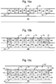
- FIGS. 15 a - 15 c are cross-sectional views illustrating stages in formation of a memory level formed according to an embodiment of the present invention.
- FIG. 16 is cross-sectional view illustrating a diode and resistive switching element that may be used an alternative embodiment of the present invention.
- FIGS. 17 a - 17 c illustrate probability plots of reverse current of devices according to a comparative example and according to examples of the present invention.
- trimmable resistors have been used as elements in integrated circuits.
- Leakage current can be greatly reduced by forming each memory cell as a two-terminal device including a diode.
- a diode has a non-linear I-V characteristic, allowing very little current flow below a turn-on voltage, and substantially higher current flow above the turn-on voltage.
- a diode also acts as one-way valves passing current more easily in one direction than the other.
- a memory element formed of doped semiconductor material for example the semiconductor diode of the '549 application, can achieve three, four, or more stable resistivity states.
- semiconductor material can be converted from an initial high-resistivity state to a lower-resistivity state; then, upon application of an appropriate electrical pulse, can be returned to a higher-resistivity state.
- These embodiments can be employed independently or combined to form a memory cell which can have two or more data states, and can be one-time-programmable or rewriteable.
- a diode between conductors in the memory cell allows its formation in a highly dense cross-point memory array.
- a polycrystalline, amorphous, or microcrystalline semiconductor memory element either is formed in series with a diode or, more preferably, is formed as the diode itself.
- transition from a higher- to a lower-resistivity state will be called a set transition, affected by a set current, a set voltage, or a set pulse; while the reverse transition, from a lower- to a higher-resistivity state, will be called a reset transition, affected by a reset current, a reset voltage, or a reset pulse.
- the reverse leakage of the diode is irrevocably increased, as shown in FIG. 5 b and as will be discussed in more detail below.
- the higher reverse leakage is a permanent feature of the diode, and the reset operation can be said to “damage” the diode. This damage is undesirable because it increases the current required to “read” large arrays of vertical diode cells, and can decrease the number of cells programmed simultaneously, reducing the “bandwidth” into the memory chip.
- the present inventors discovered that by doping the Group IV semiconductor diode, such as a silicon, germanium or silicon-germanium diode with at least one of carbon or nitrogen (or both) during fabrication, the increase in reverse or leakage current resulting from the reset operation is reduced by as much as four times, without an observed degradation in any other parameters of the cell.
- the diode reverse or leakage current determines the power consumed during read and program operations, and reduction of this leakage current can reduce power, increase the bandwidth and/or improve temperature characteristics of the cell during read and program operations.
- the diode has a leakage current of less than 4 ⁇ 10 ⁇ 10 A at ⁇ 5.5V in the high resistivity, reset state.
- the fabricated diode is doped with at least one of carbon or nitrogen in a concentration greater than an unavoidable impurity level concentration of carbon or nitrogen generally found in the silicon, germanium or silicon-germanium diode material.
- the diode is doped with carbon, nitrogen or a combination of carbon and nitrogen in a concentration of at least 1 ⁇ 10 17 cm ⁇ 3 , such as 1 ⁇ 10 17 to 1 ⁇ 10 21 cm ⁇ 3 , including 1 ⁇ 10 18 to 1 ⁇ 10 20 cm ⁇ 3 , for example 1 ⁇ 10 19 cm ⁇ 3 .
- the carbon and/or nitrogen dopant may be incorporated into the diode by any suitable method, such as ion implantation, plasma doping, vapor phase diffusion or in-situ doping during diode layer deposition.
- the diode is preferably a polycrystalline semiconductor diode, such as a polysilicon diode. However, single crystal or amorphous semiconductor diodes may also be used. In some one-time-programmable embodiments, a polycrystalline semiconductor diode is paired with a dielectric rupture antifuse, though in other embodiments the antifuse may be omitted. In use, the diode acts as a read/write element of the nonvolatile memory cell by switching from one resistivity state to a different resistivity state in response to an applied bias.
- FIG. 2 illustrates a memory cell formed according to a preferred embodiment of the present invention.
- a bottom conductor 12 is formed of a conductive material, for example tungsten, and extends in a first direction. Barrier and adhesion layers may be included in bottom conductor 12 .
- Polycrystalline semiconductor diode 2 has a bottom heavily doped n-type region 4 ; an intrinsic region 6 , which is not intentionally doped; and a top heavily doped region 8 , though the orientation of this diode may be reversed. Such a diode, regardless of its orientation, will be referred to as a p-i-n diode.
- the carbon or nitrogen is incorporated into the intrinsic region 6 such that in the p-i-n diode 2 , at least the intrinsic region 6 of the diode and optionally the p+ and the n+ regions 4 , 8 are doped with the at least one of carbon or nitrogen.
- Dielectric rupture antifuse 14 is included in some embodiments.
- Top conductor 16 may be formed in the same manner and of the same materials as bottom conductor 12 , and extends in a second direction different from the first direction.
- Polycrystalline semiconductor diode 2 is vertically disposed between bottom conductor 12 and top conductor 16 . Polycrystalline semiconductor diode 2 is formed in a high-resistivity state.
- This memory cell can be formed above a suitable substrate, for example above a monocrystalline silicon wafer.
- FIG. 3 shows a portion of a memory level of such devices formed in a cross-point array, where diodes 2 are disposed between bottom conductors 12 and top conductors 16 (antifuses 14 are omitted in this view.) Multiple memory levels can be stacked over a substrate to form a highly dense monolithic three dimensional memory array.
- an intrinsic region may in fact include a low concentration of p-type or n-type dopants. Dopants may diffuse into the intrinsic region from adjacent regions, or may be present in the deposition chamber during deposition due to contamination from an earlier deposition. It will further be understood that deposited intrinsic semiconductor material (such as silicon) may include defects which cause it to behave as if slightly n-doped. Use of the term “intrinsic” to describe silicon, germanium, a silicon-germanium alloy, or some other semiconductor material is not meant to imply that this region contains no dopants whatsoever, nor that such a region is perfectly electrically neutral.
- the resistivity of doped polycrystalline or microcrystalline semiconductor material can be changed between stable states by applying appropriate electrical pulses. It has been found that in preferred embodiments, set transitions are advantageously performed with the diode under forward bias, while reset transitions are most readily achieved and controlled with the diode under reverse bias. In some instances, however, set transitions may be achieved with the diode under reverse bias, while reset transitions are achieved with the diode under forward bias.
- Switching under reverse bias shows a distinct behavior.
- a polysilicon p-i-n diode like the one shown in FIG. 2 is subjected to a relatively large switching pulse under reverse bias.
- a smaller read pulse for example 2 volts
- the read current is measured.
- the subsequent read current at two volts changes as shown in FIG. 4 . It will be seen that initially as the reverse voltage and current of the switching pulse are increased, the read current, when a read voltage is applied after each switching pulse, increases; i.e.
- the initial transition of the semiconductor material (silicon, in this case) is in the set direction toward lower resistivity.
- the switching pulse reaches a certain reverse bias voltage, at point K in FIG. 4 , about ⁇ 14.6 volts in this example, the read current abruptly begins to drop as reset is achieved and resistivity of the silicon increases.
- the switching voltage at which the set trend is reversed and the silicon of the diode begins to reset varies, depending on, for example, the resistivity state of the silicon making up the diode when application of the reverse bias switching pulse is begun. It will be seen, then, that by selecting appropriate voltages, either set or reset of the semiconductor material making up the diode can be achieved with the diode under reverse bias.
- Distinct data states of the memory cell of the embodiments of the present invention correspond to resistivity states of polycrystalline or microcrystalline semiconductor material making up the diode, which are distinguished by detecting current flow through the memory cell (between top conductor 16 and bottom conductor 12 ) when a read voltage is applied.
- the current flowing between any one distinct data state and any different distinct data state is at least a factor of two, to allow the difference between the states to be readily detectable.
- the memory cell can be used as a one-time programmable cell or a rewriteable memory cell, and may have two, three, four, or more distinct data states.
- the cell can be converted from any of its data states to any other of its data states in any order, and under either forward or reverse bias.
- a diode formed of polycrystalline semiconductor material and a dielectric rupture antifuse are arranged in series disposed between a top and bottom conductor.
- the two-terminal device is used as a one-time-programmable multilevel cell, in preferred embodiments having three or four distinct data states.
- Diode 2 is preferably formed of a polycrystalline or microcrystalline semiconductor material, for example silicon, germanium, or an alloy of silicon and/or germanium. Diode 2 is most preferably polysilicon. In this example, bottom heavily doped region 4 is n-type and top heavily doped region 8 is p-type, though the polarity of the diode may be reversed.
- the memory cell comprises a portion of the top conductor, a portion of the bottom conductor, and a diode, the diode disposed between the conductors.
- FIG. 5 a is a probability plot showing current of a memory cells in various states. It should be noted that the probability plots shown in FIGS. 5 a , 6 , 7 , 9 and 11 illustrate exemplary embodiments of various programming methods using a cell containing a diode that is not doped with carbon or nitrogen. The programming methods for a cell containing a diode that is doped with carbon or nitrogen are similar to those methods. Turning to FIG.
- Area V on the graph of FIG. 5 a corresponds to a first data state of the memory cell. For some memory cells in the array, this cell will not be subjected to set or reset pulses, and this state will be read as a data state of the memory cell. This first data state will be referred to as the V state.
- a first electrical pulse preferably with diode 2 under forward bias, is applied between top conductor 16 and bottom conductor 12 .
- This pulse is, for example, between about 8 volts and about 12 volts, for example about 10 volts.
- the current is, for example, between about 80 and about 200 microamps.
- the pulse width is preferably between about 100 and about 500 nsec.
- This first electrical pulse ruptures dielectric rupture antifuse 14 and switches the semiconductor material of diode 2 from a first resistivity state to a second resistivity state, the second state lower resistivity than the first.
- This second data state will be referred to as the P state, and this transition is labeled “V ⁇ P” in FIG. 5 a .
- the current flowing between top conductor 16 and bottom conductor 12 at a read voltage of 2 volts is about 10 microamps or more.
- the resistivity of the semiconductor material making up diode 2 is reduced by a factor of about 1000 to about 2000. In other embodiments the change in resistivity will be less, but between any data state and any other data state will be at least a factor of two, preferably at least a factor of three or five, and more typically a factor of 100 or more. Some memory cells in the array will be read at this data state, and will not be subjected to additional set or reset pulses. This second data state will be referred to as the P state.
- the read current at 2V can increase from 1 ⁇ 10 ⁇ 8 A in the unprogrammed state to at least 1 ⁇ 10 ⁇ 5 A after the programming pulse.
- the table below shows that increasing the programming voltage results in a higher read current.
- the last column in the table shows the standard deviation of the read current.
- the read currents shown in the table above are for a cell shown FIG. 2 with the interconnects and a silicon oxide antifuse. If the interconnects are excluded, then the read current is even higher.
- the read current of the cell without the interconnects is at least 3.5 ⁇ 10 ⁇ 5 A at a read voltage of at least +1.5V, such as +1.5 to +2V. It is expected that further increases in programming voltage would provide a further increase in the read current.
- increasing the programming voltage from 8.4V to 10V is expected to generate an about 70% increase in read current, such that the read current for a cell without the interconnects is about 6 ⁇ 10 ⁇ 5 A at 2V read voltage.
- multiple programming pulses such as 2 to 10 pulses, for example 3-5 pulses, may be applied to the diode.
- a second electrical pulse preferably with diode 2 under reverse bias, is applied between top conductor 16 and bottom conductor 12 .
- This pulse is, for example, between about ⁇ 8 volts and about ⁇ 14 volts, preferably about between about ⁇ 10 and about ⁇ 12 volts, preferably about ⁇ 11 volts.
- the current is, for example, between about 80 and about 200 microamps.
- the pulse width is, for example, between about 100 nanosec and about 10 microseconds; preferably between about 100 nsec and about 1 microsecond, most preferably between about 200 and about 800 nsec.
- This second electrical pulse switches the semiconductor material of diode 2 from the second resistivity state to a third resistivity state, the third resistivity state higher resistivity than the second.
- the current flowing between top conductor 16 and bottom conductor 12 at a read voltage of 2 volts is between about 10 and about 500 nanoamps, preferably between about 100 and about 500 nanoamps. Some memory cells in the array will be read at this data state, and will not be subjected to additional set or reset pulses.
- This third data state will be referred to as the R state, and this transition is labeled “P ⁇ R” in FIG. 5 a.
- FIG. 5 b is a plot of read current versus read voltage for various diode states illustrated in FIG. 5 a .
- the diode initially starts in a low read current state V (referred to as the unprogrammed or “virgin” state).
- the diode is put the in the programmed state P by the high forward bias pulse, preferably at the factory where the diode is made before the product is sold, where power is not a consideration.
- the diode is subsequently put in the reset state R by a reverse bias programming pulse.
- the difference between the read currents of the programmed and reset states P and R constitutes the “window” for the memory cell, as shown in FIG. 5 b .
- the large programming voltage and/or multiple programming pulses allow this window to be as large as possible for manufacturing robustness.
- a third electrical pulse preferably with diode 2 under forward bias, is applied between top conductor 16 and bottom conductor 12 .
- This pulse is, for example, between about 8 volts and about 12 volts, for example about 10 volts, with current between about 5 and about 20 microamps.
- This third electrical pulse switches the semiconductor material of diode 2 from the third resistivity state to a fourth resistivity state, the fourth resistivity state lower resistivity than the third, and preferably higher resistivity than the second resistivity state.
- the current flowing between top conductor 16 and bottom conductor 12 at a read voltage of 2 volts is between about 1.5 and about 4.5 microamps.
- the difference in current at the read voltage is preferably at least a factor of two between any two adjacent data states.
- the read current of any cell in data state R is preferably at least two times that of any cell in data state V
- the read current of any cell in data state S is preferably at least two times that of any cell in data state R
- the read current of a cell in data state P is preferably at least two times that of any cell in data state S.
- the read current at data state R may be two times the read current at data state V
- the read current at data state S may be two times the read current at data state R
- the read current at data state P may be two times the read current at data state S.
- the difference could be considerably larger; for example, if the highest-current V state cell can have a read current of 5 nanoamps and the lowest-current R state call can have a read current of 100 nanoamps, the difference in current is at least a factor of 20. By selecting other limits, it can be assured that the difference in read current between adjacent memory states will be at least a factor of three.
- an iterative read-verify-write process may be applied to assure that a memory cell is in one of the defined data states after a set or reset pulse, and not between them.
- a memory cell having four distinct data states has been described. To aid in distinguishing between the data states, it may be preferred for three rather than four data states to be selected.
- a three-state memory cell can be formed in data state V, set to data state P, then reset to data state R. This cell will have no fourth data state S.
- the difference between adjacent data states for example between the R and P data states, can be significantly larger.
- the cells may be programmed in a variety of ways, however.
- the memory cell of FIG. 2 may be formed in a first state, the V state.
- a first electrical pulse preferably under forward bias, ruptures antifuse 14 and switches the polysilicon of the diode from a first resistivity state to a second resistivity state lower than the first, placing the memory cell in the P state, which in this example is the lowest resistivity state.
- a second electrical pulse preferably under reverse bias, switches the polysilicon of the diode from the second resistivity state to a third resistivity state, the third resistivity state higher resistivity than the second, placing the memory cell in the S state.
- a third electrical pulse preferably also under reverse bias, switches the polysilicon of the diode from the third resistivity state to a fourth resistivity state, the third resistivity state higher resistivity than the second, placing the memory cell in the R state.
- any of the data states, the V state, the R state, the S state, and the P state can be read as a data state of the memory cell.
- Each transition is labeled in FIG. 6 . Four distinct states are shown; there could be three or more than four states as desired.
- each successive electrical pulse can switch the semiconductor material of the diode to a successively lower resistivity state.
- the memory cell can proceed from the initial V state to the R state, from the R state to the S state, and from the S state to the P state, where for each state the read current is at least two times the read current at the previous state, each corresponding to a distinct data state.
- This scheme may be most advantageous when there is no antifuse included in the cell.
- the pulses may be applied under either forward or reverse bias. In alternative embodiments there may be three data states or more than four data states.
- a memory cell includes the polysilicon or microcrystalline diode 2 shown in FIG. 8 , including bottom heavily doped p-type region 4 , middle intrinsic or lightly doped region 6 , and top heavily doped n-type region 8 .
- this diode 2 can be arranged in series with a dielectric rupture antifuse, the two disposed between top and bottom conductors.
- Bottom heavily doped p-type region 4 may be in situ doped, i.e. doped by flowing a gas that provides a p-type dopant such as boron during deposition of the polysilicon, such that dopant atoms are incorporated into the film as it forms.
- this memory cell is formed in the V state, where the current between top conductor 16 and bottom conductor 12 is less than about 80 nanoamps at a read voltage of 2 volts.
- a first electrical pulse preferably applied under forward bias of, for example, about 8 volts, ruptures dielectric rupture antifuse 14 , if it is present, and switches the polysilicon of diode 2 from a first resistivity state to a second resistivity state, the second resistivity state lower than the first, placing the memory cell in data state P.
- data state P the current between top conductor 16 and bottom conductor 12 at the read voltage is between about 1 microamp and about 4 microamps.
- a second electrical pulse preferably applied in reverse bias, switches the polysilicon of diode 2 from the second resistivity state to a third resistivity state, the third resistivity state lower than the first.
- the third resistivity state corresponds to data state M.
- data state M the current between top conductor 16 and bottom conductor 12 at the read voltage is above about 10 microamps.
- the difference in current between any cell in adjacent data states is preferably at least a factor of two, preferably a factor of three or more. Any of the data states V, P, or M can be detected as a data state of the memory cell.
- FIG. 4 showed that when a semiconductor diode is subjected to reverse bias, in general the semiconductor material initially undergoes a set transition to lower resistivity, then, as voltage is increased, undergoes a reset transition to higher resistivity.
- the switch from set transition to reset transition with increasing reverse bias voltage does not occur as abruptly or as steeply as with other embodiments of the diode. This means a set transition under reverse bias is easier to control with such a diode.
- the memory cell behaves as a rewriteable memory cell, which is repeatably switchable between two or between three data states.
- FIG. 10 shows a memory cell that may serve as a rewriteable memory cell.
- This memory cell is the same as the one shown in FIG. 2 , except no dielectric rupture antifuse is included. Most rewriteable embodiments do not include an antifuse in the memory cell, though one may be included if desired. It should be noted that TiN layers may be included in the cell above and below the diode, as will be described in more detail with respect to FIGS. 15 a - 15 c below.
- the memory cell is formed in a high resistivity state V, with current at 2 volts about 5 nanoamps or less.
- V high resistivity state
- the initial V state does not serve as a data state of the memory cell.
- a first electrical pulse preferably with diode 2 under forward bias, is applied between top conductor 16 and bottom conductor 12 . This pulse is, for example, between about 8 and about 12 volts, preferably about 10 volts. This first electrical pulse switches the semiconductor material of diode 2 from a first resistivity state to a second resistivity state P, the second state lower resistivity than the first.
- the P state also will not serve as a data state of the memory cell. In other embodiments, the P state will serve as a data state of the memory cell.
- a second electrical pulse preferably with diode 2 under reverse bias, is applied between top conductor 16 and bottom conductor 12 .
- This pulse is, for example, between about ⁇ 8 and about ⁇ 14 volts, preferably between about ⁇ 9 and about ⁇ 13 volts, more preferably about ⁇ 10 or ⁇ 11 volts.
- the voltage required will vary with the thickness of the intrinsic region.
- This second electrical pulse switches the semiconductor material of diode 2 from the second resistivity state to a third resistivity state R, the third state higher resistivity than the second.
- the R state corresponds to a data state of the memory cell.
- a third electrical pulse can be applied between top conductor 16 and bottom conductor 12 , preferably under forward bias.
- This pulse is, for example, between about 5.5 and about 9 volts, preferably about 6.5 volts, with current between about 10 and about 200 microamps, preferably between about 50 and about 100 microamps.
- This third electrical pulse switches the semiconductor material of diode 2 from the third resistivity state R to a fourth resistivity state S, the fourth state lower resistivity than the third.
- the S state corresponds to a data state of the memory cell.
- the R state and the S state are sensed, or read, as data states.
- the memory cell can repeatedly be switched between these two states. For example, a fourth electrical pulse, preferably with diode 2 under reverse bias, switches the semiconductor material of the diode from the fourth resistivity state S to the fifth resistivity state R, which is substantially the same as the third resistivity state R.
- a fifth electrical pulse preferably with diode 2 under forward bias, switches the semiconductor material of the diode from the fifth resistivity state R to the sixth resistivity state S, which is substantially the same as the fourth resistivity state S, and so on.
- both the first electrical pulse, which switches the cell from the initial V state to the P state, and the second electrical pulse, which switches the cell from the P state to the R state, may be performed before the memory array reaches the end user, for example in a factory or test facility, or by a distributor before sale.
- the difference between current flow under read voltage, for example of 2 volts, between top conductor 16 and bottom conductor 12 between any cell in one data state and any cell in an adjacent data states, in this case the R data state (between about 10 and about 500 nanoamps) and the S data state (between about 1.5 and about 4.5 microamps), is at least a factor of three.
- the difference may be a factor of two, three, five, or more.
- a rewriteable memory cell can be switched between three or more data states, in any order. Either set or reset transitions can be performed with the diode under either forward or reverse bias.
- the data state corresponds to the resistivity state of polycrystalline or microcrystalline semiconductor material making up a diode.
- the data states does not correspond to the resistivity state of a resistivity-switching metal oxide or nitride, as in Herner et al., U.S. patent application Ser. No. 11/395,995, “Nonvolatile Memory Cell Comprising a Diode and a Resistance-Switching Material,” filed Mar. 31, 2006, owned by the assignee of the present invention and hereby incorporated by reference.
- any step in which cells are subjected to large voltages in reverse bias has reduced leakage current as compared to a forward bias step.
- Bitline B 0 is set at 10 volts and wordline W 0 is set at ground.
- wordline W 1 is set less than but relatively close to the voltage of bitline B 0 ; for example wordline W 1 may be set to 9.3 volts, so that 0.7 volts is applied across the F cells (only one F cell is shown, but there may be hundreds, thousands or more.)
- bitline B 1 is set higher than but relatively close to the voltage of wordline W 0 ; for example bitline B 1 may be set to 0.7 volts, so that 0.7 volts is applied across cell H (again, there may be thousands of H cells.)
- the unselected cells U which share neither wordline W 0 or bitline B 0 with selected cell S, are subjected to ⁇ 8.6 volts. As there may be millions of unselected cells U
- FIG. 13 shows an advantageous biasing scheme to apply a large reverse bias across a memory cell, for example as a reset pulse.
- Bitline B 0 is set at ⁇ 5 volts and wordline W 0 at 5 volts, so that ⁇ 10 volts is applied across selected cell S; the diode is in reverse bias.
- Setting wordline W 1 and bitline B 1 at ground subjects both half-selected cells F and H to ⁇ 5 volts, at a reverse bias low enough not to cause unintentional set or reset of these cells.
- Set or reset in reverse bias generally seems to take place at or near the voltage at which the diode goes into reverse breakdown, which is generally higher than ⁇ 5 volts.
- bitline B 0 can be set at 0 volts, wordline W 0 at ⁇ 10 volts, and bitline B 1 and wordline W 1 at ⁇ 5 volts.
- the voltage across selected cell S, half-selected cells H and F, and unselected cells U will be the same as in the scheme of FIG. 13 .
- bitline B 0 is set at ground, wordline W 0 at 10 volts, and bitline B 1 and wordline W 1 each at 5 volts.
- the difference between current flow during read in adjacent data states is preferably at least a factor of two; in many embodiments, it may be preferred to establish current ranges for each data state which are separated by a factor of three, five, ten, or more.
- data state V may be defined as read current of 5 nanoamps or less at a read voltage of 2 volts, data state R as read current between about 10 and about 500 nanoamps, data state S as read current between about 1.5 and about 4.5 microamps, and data state P as read current above about 10 microamps.
- data state V may be defined in a smaller range, with read current about 5 nanoamps or less at a read voltage of 2 volts. Actual read currents will vary with characteristics of the cell, construction of the array, read voltage selected, and many other factors.
- a one-time programmable memory cell is in data state P.
- An electrical pulse in reverse bias is applied to the memory cell to switch the cell into data state S.
- the read current is not in the desired range; i.e. the resistivity state of the semiconductor material of the diode is higher or lower than intended.
- the read current of the memory cell is at the point on the graph shown at Q, in between the S state and P state current ranges.
- the memory cell may be read to determine if the desired data state was reached. If the desired data state was not reached, an additional pulse is applied. For example, when the current Q is sensed, an additional reset pulse is applied to increase the resistivity of the semiconductor material, decreasing the read current into the range corresponding to the S data state. As described earlier, this set pulse may be applied in either forward or reverse bias. The additional pulse or pulses may have a higher amplitude (voltage or current) or longer or shorter pulse width than the original pulse. After the additional set pulse, the cell is read again, then set or reset pulses applied as appropriate until the read current is in the desired range.
- a two-terminal device such as the memory cell including a diode described
- Applying a large reverse bias across the diode may damage the diode; thus when performing a set or reset with the diode under reverse bias, it is advantageous to minimize the reverse bias voltage.
- an amorphous or microcrystalline silicon material is crystallized not in contact with a silicon having a silicide with which it has a good lattice match, for example in contact only with materials such as silicon dioxide and titanium nitride, with which it has a significant lattice mismatch, the resulting polysilicon will have many more defects, and doped polysilicon crystallized this way will be much less conductive as formed.
- the semiconductor material forming a diode is switched between two or more resistivity states, changing the current flowing through the diode at a given read voltage, the different currents (and resistivity states) corresponding to distinct data states. It has been found that diodes formed of high-defect silicon (or other appropriate semiconductor materials such as germanium or silicon-germanium alloys) which has not been crystallized adjacent to a silicide or analogous material providing a crystallization template exhibit the most advantageous switching behavior.
- the resistivity state of very low-defect silicon crystallized adjacent to an appropriate silicide cannot be switched as readily as when the semiconductor material has a higher concentration of intragrain (e.g. microtwin) defects. It may be that the presence of defects, or of a larger number of grain boundaries, allows for easier switching.
- the polycrystalline or microcrystalline material forming the diode is not crystallized adjacent to a material with which it has a small lattice mismatch.
- a small lattice mismatch is, for example, a lattice mismatch of about three percent or less.
- switching behavior may be centered on changes in the intrinsic region. Switching behavior has been observed in resistors and p-n diodes as well, and is not limited to p-i-n diodes, but it is believed that the use of p-i-n diodes may be particularly advantageous.
- a fabrication method of a single memory level according to one embodiment of the invention will be described in detail. Additional memory levels can be stacked, each monolithically formed above the one below it. In this embodiment, a polycrystalline semiconductor diode will serve as the switchable memory element.
- This substrate 100 can be any semiconducting substrate as known in the art, such as monocrystalline silicon, IV-IV compounds like silicon-germanium or silicon-germanium-carbon, III-V compounds, II-VII compounds, epitaxial layers over such substrates, or any other semiconducting material.
- the substrate may include integrated circuits fabricated therein.
- the insulating layer 102 is formed over substrate 100 .
- the insulating layer 102 can be silicon oxide, silicon nitride, high-dielectric film, Si—C—O—H film, or any other suitable insulating material.
- the first conductors 200 are formed over the substrate and insulator.
- An adhesion layer 104 may be included between the insulating layer 102 and the conducting layer 106 to help conducting layer 106 adhere to insulating layer 102 . If the overlying conducting layer is tungsten, titanium nitride is preferred as adhesion layer 104 .
- Conducting layer 106 can comprise any conducting material known in the art, such as tungsten, or other materials, including tantalum, titanium, copper, cobalt, or alloys thereof.
- the layers will be patterned and etched using any suitable masking and etching process to form substantially parallel, substantially coplanar conductors 200 , shown in FIG. 15 a in cross-section.
- photoresist is deposited, patterned by photolithography and the layers etched, and then the photoresist removed using standard process techniques.
- Conductors 200 could be formed by a Damascene method instead.
- Dielectric material 108 is deposited over and between conductor rails 200 .
- Dielectric material 108 can be any known electrically insulating material, such as silicon oxide, silicon nitride, or silicon oxynitride. In a preferred embodiment, silicon dioxide is used as dielectric material 108 .
- FIG. 15 a This removal of dielectric overfill to form planar surface 109 can be performed by any process known in the art, such as chemical mechanical planarization (CMP) or etchback.
- CMP chemical mechanical planarization
- An etchback technique that may advantageously be used is described in Raghuram et al., U.S. application Ser. No. 10/883,417, “Nonselective Unpatterned Etchback to Expose Buried Patterned Features,” filed Jun. 30, 2004 and hereby incorporated by reference.
- a plurality of substantially parallel first conductors have been formed at a first height above substrate 100 .
- a barrier layer 110 is deposited as the first layer after planarization of the conductor rails.
- Any suitable material can be used in the barrier layer, including tungsten nitride, tantalum nitride, titanium nitride, or combinations of these materials.
- titanium nitride is used as the barrier layer.
- the barrier layer is titanium nitride, it can be deposited in the same manner as the adhesion layer described earlier.
- the semiconductor material can be silicon, germanium, a silicon-germanium alloy, or other suitable semiconductors, or semiconductor alloys.
- silicon germanium
- a silicon-germanium alloy or other suitable semiconductors, or semiconductor alloys.
- this description will refer to the semiconductor material as silicon, but it will be understood that the skilled practitioner may select any of these other suitable materials instead.
- the pillar comprises a semiconductor junction diode.
- junction diode is used herein to refer to a semiconductor device with the property of non-ohmic conduction, having two terminal electrodes, and made of semiconducting material which is p-type at one electrode and n-type at the other. Examples include p-n diodes and n-p diodes, which have p-type semiconductor material and n-type semiconductor material in contact, such as Zener diodes, and p-i-n diodes, in which intrinsic (undoped) semiconductor material is interposed between p-type semiconductor material and n-type semiconductor material.
- Bottom heavily doped region 112 can be formed by any deposition and doping method known in the art.
- the silicon can be deposited and then doped, but is preferably doped in situ by flowing a donor gas providing n-type dopant atoms, for example phosphorus, during deposition of the silicon.
- Heavily doped region 112 is preferably between about 100 and about 800 angstroms thick.
- Intrinsic layer 114 can be formed by any method known in the art.
- Layer 114 can be silicon, germanium, or any alloy of silicon or germanium and has a thickness between about 1100 and about 3300 angstroms, preferably about 2000 angstroms.
- Pillars 300 should have about the same pitch and about the same width as conductors 200 below, such that each pillar 300 is formed on top of a conductor 200 . Some misalignment can be tolerated.
- the pillars 300 can be formed using any suitable masking and etching process.
- photoresist can be deposited, patterned using standard photolithography techniques, and etched, then the photoresist removed.
- a hard mask of some other material for example silicon dioxide, can be formed on top of the semiconductor layer stack, with bottom antireflective coating (BARC) on top, then patterned and etched.
- BARC bottom antireflective coating
- DARC dielectric antireflective coating
- Dielectric material 108 is deposited over and between the semiconductor pillars 300 , filling the gaps between them.
- Dielectric material 108 can be any known electrically insulating material, such as silicon oxide, silicon nitride, or silicon oxynitride. In a preferred embodiment, silicon dioxide is used as the insulating material.
- dielectric material on top of the pillars 300 is removed, exposing the tops of pillars 300 separated by dielectric material 108 , and leaving a substantially planar surface.
- This removal of dielectric overfill can be performed by any process known in the art, such as CMP or etchback.
- CMP or etchback ion implantation is performed, forming heavily doped p-type top region 116 .
- the p-type dopant is preferably boron or BCl 3 .
- This implant step completes formation of diodes 111 .
- the resulting structure is shown in FIG. 15 b . In the diodes just formed, bottom heavily doped regions 112 are n-type while top heavily doped regions 116 are p-type; clearly the polarity could be reversed.
- the carbon and/or nitrogen dopant may be incorporated into the diode by any suitable methods, such as ion implantation, plasma doping, vapor phase diffusion or in-situ doping during diode layer deposition during any suitable time in the diode fabrication process, preferably prior to the formation of the upper electrode over the diode.
- carbon and/or nitrogen may be ion implanted into the diode after the dielectric overfill planarization step.
- the carbon and/or nitrogen ion implant may be conducted before or after the p+ ion implant.
- the carbon and/or nitrogen ion implant may be conducted after deposition of the intrinsic regions 114 but before the deposition of the p+ regions 116 .
- the diode region(s) 114 and/or 116 may be exposed to a nitrogen and/or carbon containing gas or plasma after the regions 114 and/or 116 are deposited to dope these regions 114 and/or 116 with carbon and/or nitrogen.
- a carbon and/or nitrogen containing gas such as methane or ammonia, for example
- the silicon or germanium containing source gas such as silane or germane
- Antifuse 118 is preferably a silicon dioxide layer formed by oxidizing the underlying silicon in a rapid thermal anneal, for example at about 600 degrees. Antifuse 118 may be about 10 to about 100, such as about 20 to about 40 angstroms thick. Alternatively, antifuse 118 can be deposited. Top conductors 400 can be formed in the same manner as bottom conductors 200 , for example by depositing adhesion layer 120 , preferably of titanium nitride, and conductive layer 122 , preferably of tungsten.
- Conductive layer 122 and adhesion layer 120 are then patterned and etched using any suitable masking and etching technique to form substantially parallel, substantially coplanar conductors 400 , shown in FIG. 15 c extending left-to-right across the page.
- photoresist is deposited, patterned by photolithography and the layers etched, and then the photoresist removed using standard process techniques.
- the dielectric material can be any known electrically insulating material, such as silicon oxide, silicon nitride, or silicon oxynitride. In a preferred embodiment, silicon oxide is used as this dielectric material.
- Formation of a first memory level has been described. Additional memory levels can be formed above this first memory level to form a monolithic three dimensional memory array.
- conductors can be shared between memory levels; i.e. top conductor 400 would serve as the bottom conductor of the next memory level.
- an interlevel dielectric (not shown) is formed above the first memory level of FIG. 15 c , its surface planarized, and construction of a second memory level begins on this planarized interlevel dielectric, with no shared conductors.
- a monolithic three dimensional memory array is one in which multiple memory levels are formed above a single substrate, such as a wafer, with no intervening substrates.
- the layers forming one memory level are deposited or grown directly over the layers of an existing level or levels.
- stacked memories have been constructed by forming memory levels on separate substrates and adhering the memory levels atop each other, as in Leedy, U.S. Pat. No. 5,915,167, “Three dimensional structure memory.”
- the substrates may be thinned or removed from the memory levels before bonding, but as the memory levels are initially formed over separate substrates, such memories are not true monolithic three dimensional memory arrays.
- a monolithic three dimensional memory array formed above a substrate comprises at least a first memory level formed at a first height above the substrate and a second memory level formed at a second height different from the first height. Three, four, eight, or indeed any number of memory levels can be formed above the substrate in such a multilevel array.
- FIG. 16 shows a switchable memory element 117 formed in series with a diode 111 .
- the switchable memory element 117 is formed of semiconductor material which is switched between resistivity states using electrical pulses as described.
- the diode is preferably crystallized adjacent to a silicide such as cobalt silicide, which provides a crystallization template, as described earlier, such that the semiconductor material of the diode is very low-defect and exhibits little or no switching behavior.
- Switchable memory element 117 is preferably doped, and should be doped to the same conductivity type as top heavily doped region 116 . Methods to fabricate this device are described in U.S. application Ser. No. 11/237,167, filed on Sep. 28, 2005 and incorporated by reference herein in its entirety.
- FIGS. 17 a - 17 c illustrate probability plots of devices according to non-limiting examples of the present invention. Specifically, the figures are probability plots of devices containing 24 memory cells per wafer, showing the reverse leakage current at ⁇ 5.5V bias at about room temperature, after the initial set (or program) and reset operations.
- FIG. 17 a shows a device of a comparative example in which the diodes were not intentionally doped with carbon or nitrogen (i.e., there were no implants into the diode other than the p + implant). The median diode reverse leakage after reset is 4.5 ⁇ 10 ⁇ 10 A.
- FIG. 17 b shows a device of an example of the present invention in which the diode received a 50 keV N + implant to a dose of 2 ⁇ 10 15 /cm 2 in addition to the p + implant.
- the median diode reverse leakage after reset is 1.3 ⁇ 10 ⁇ 10 A.
- FIG. 17 c shows a device of another example of the present invention in which the diode received a 50 keV C + implant to a dose of 5 ⁇ 10 15 /cm 2 in addition to the p + implant.
- the median diode reverse leakage after reset is 3.3 ⁇ 10 ⁇ 10 A.
- the reverse or leakage current is substantially lower for the devices implanted with nitrogen or carbon than with a device which was not intentionally doped with nitrogen or carbon.
- the devices in which the diodes were implanted with carbon or nitrogen had a leakage current of less than 4 ⁇ 10 ⁇ 10 A (such as 1.3 to 3.3 ⁇ 10 ⁇ 10 A) at ⁇ 5.5V in the high resistivity, reset state, while the device of the comparative example had a leakage current of greater than 4 ⁇ 10 ⁇ 10 A (4.5 ⁇ 10 ⁇ 10 A) at ⁇ 5.5V in the high resistivity, reset state.
- the inventors believe that the carbon or nitrogen species may bond to dangling bonds in the silicon diode passivating them. Reducing or eliminating the dangling bonds as a source of electrically active defects in the diode may reduce the leakage current.
Abstract
Description
| Programming | Programmed | |
| Pulse Voltage | Read Current @ +2 V | 1σ |
| +6.4 V | 1.1 × 10⁻⁵ A | 6.1 × 10⁻⁶ A |
| +7.4 V | 1.7 × 10⁻⁵ A | 7.2 × 10⁻⁶ A |
| +8.4 V | 1.8 × 10⁻⁵ A | 5.4 × 10⁻⁶ A |
Claims (21)
Priority Applications (7)
| Application Number | Priority Date | Filing Date | Title |
|---|---|---|---|
| US11/819,041 US8072791B2 (en) | 2007-06-25 | 2007-06-25 | Method of making nonvolatile memory device containing carbon or nitrogen doped diode |
| JP2010513271A JP5545872B2 (en) | 2007-06-25 | 2008-06-23 | Nonvolatile memory device including diode doped with carbon or nitrogen and method of manufacturing the same |
| EP08768725.7A EP2168161B1 (en) | 2007-06-25 | 2008-06-23 | Nonvolatile memory device containing carbon or nitrogen doped diode and method of making thereof |
| PCT/US2008/007801 WO2009002476A2 (en) | 2007-06-25 | 2008-06-23 | Nonvolatile memory device containing a carbon- or nitrogen-doped diode and methods of making andoperating the same |
| KR1020107001563A KR20100055392A (en) | 2007-06-25 | 2008-06-23 | Nonvolatile memory device containing a carbon- or nitrogen-doped diode and methods of making and operating the same |
| CN2008800214041A CN101720507B (en) | 2007-06-25 | 2008-06-23 | Nonvolatile memory device containing carbon or nitrogen doped diode and method of making and operating same |
| TW097123543A TWI508307B (en) | 2007-06-25 | 2008-06-24 | Nonvolatile memory device containing carbon or nitrogen doped diode and method of making thereof |
Applications Claiming Priority (1)
| Application Number | Priority Date | Filing Date | Title |
|---|---|---|---|
| US11/819,041 US8072791B2 (en) | 2007-06-25 | 2007-06-25 | Method of making nonvolatile memory device containing carbon or nitrogen doped diode |
Publications (2)
| Publication Number | Publication Date |
|---|---|
| US20080316795A1 US20080316795A1 (en) | 2008-12-25 |
| US8072791B2 true US8072791B2 (en) | 2011-12-06 |
Family
ID=40136299
Family Applications (1)
| Application Number | Title | Priority Date | Filing Date |
|---|---|---|---|
| US11/819,041 Expired - Fee Related US8072791B2 (en) | 2007-06-25 | 2007-06-25 | Method of making nonvolatile memory device containing carbon or nitrogen doped diode |
Country Status (1)
| Country | Link |
|---|---|
| US (1) | US8072791B2 (en) |
Cited By (5)
| Publication number | Priority date | Publication date | Assignee | Title |
|---|---|---|---|---|
| US20110133149A1 (en) * | 2009-12-04 | 2011-06-09 | Sonehara Takeshi | Resistance change memory and manufacturing method thereof |
| US20130062589A1 (en) * | 2009-06-18 | 2013-03-14 | Nobuaki Yasutake | Resistance change memory |
| US20150078061A1 (en) * | 2012-05-29 | 2015-03-19 | Panasonic Corporation | Semiconductor memory device and semiconductor device mounting the semiconductor memory device |
| US9640586B2 (en) | 2014-06-18 | 2017-05-02 | Samsung Electronics Co., Ltd. | Semiconductor diodes, and variable resistance memory devices |
| US10741753B2 (en) | 2016-03-11 | 2020-08-11 | Micron Technology, Inc. | Conductive hard mask for memory device formation |
Families Citing this family (10)
| Publication number | Priority date | Publication date | Assignee | Title |
|---|---|---|---|---|
| US7307268B2 (en) | 2005-01-19 | 2007-12-11 | Sandisk Corporation | Structure and method for biasing phase change memory array for reliable writing |
| US7706169B2 (en) * | 2007-12-27 | 2010-04-27 | Sandisk 3D Llc | Large capacity one-time programmable memory cell using metal oxides |
| KR20130043533A (en) * | 2011-10-20 | 2013-04-30 | 삼성전자주식회사 | Non-volatile memory device having conductive buffer pattern and method of forming the same |
| US9864138B2 (en) | 2015-01-05 | 2018-01-09 | The Research Foundation For The State University Of New York | Integrated photonics including germanium |
| US10976491B2 (en) | 2016-11-23 | 2021-04-13 | The Research Foundation For The State University Of New York | Photonics interposer optoelectronics |
| US10698156B2 (en) | 2017-04-27 | 2020-06-30 | The Research Foundation For The State University Of New York | Wafer scale bonded active photonics interposer |
| EP3776074B1 (en) | 2018-04-04 | 2023-11-22 | The Research Foundation for the State University of New York | Heterogeneous structure on an integrated photonics platform |
| US10816724B2 (en) | 2018-04-05 | 2020-10-27 | The Research Foundation For The State University Of New York | Fabricating photonics structure light signal transmission regions |
| US11550099B2 (en) | 2018-11-21 | 2023-01-10 | The Research Foundation For The State University Of New York | Photonics optoelectrical system |
| TWI829761B (en) | 2018-11-21 | 2024-01-21 | 紐約州立大學研究基金會 | Photonics structure with integrated laser |
Citations (63)
| Publication number | Priority date | Publication date | Assignee | Title |
|---|---|---|---|---|
| US4062033A (en) * | 1975-04-25 | 1977-12-06 | Sony Corporation | Schottky barrier type semiconductor device |
| US4167791A (en) | 1978-01-25 | 1979-09-11 | Banavar Jayanth R | Non-volatile information storage arrays of cryogenic pin diodes |
| GB2098798A (en) | 1981-05-15 | 1982-11-24 | Philips Electronic Associated | Method of making silicon semiconductor devices |
| US4646266A (en) | 1984-09-28 | 1987-02-24 | Energy Conversion Devices, Inc. | Programmable semiconductor structures and methods for using the same |
| US4665428A (en) | 1984-01-13 | 1987-05-12 | The British Petroleum Company P.L.C. | Semiconductor device |
| EP0520561A2 (en) | 1991-06-26 | 1992-12-30 | Philips Electronics Uk Limited | Thin-film ROM devices and their manufacture |
| US5212101A (en) * | 1989-04-14 | 1993-05-18 | Secretary Of State For Defence In Her Britannic Majesty's Government Of The United Kingdom | Substitutional carbon in silicon |
| US5432729A (en) | 1993-04-23 | 1995-07-11 | Irvine Sensors Corporation | Electronic module comprising a stack of IC chips each interacting with an IC chip secured to the stack |
| US5441901A (en) * | 1993-10-05 | 1995-08-15 | Motorola, Inc. | Method for forming a carbon doped silicon semiconductor device having a narrowed bandgap characteristic |
| US5559732A (en) | 1994-12-27 | 1996-09-24 | Syracuse University | Branched photocycle optical memory device |
| US5693556A (en) | 1995-12-29 | 1997-12-02 | Cypress Semiconductor Corp. | Method of making an antifuse metal post structure |
| US5709745A (en) * | 1993-01-25 | 1998-01-20 | Ohio Aerospace Institute | Compound semi-conductors and controlled doping thereof |
| US5745407A (en) | 1994-05-05 | 1998-04-28 | California Institute Of Technology | Transistorless, multistable current-mode memory cells and memory arrays and methods of reading and writing to the same |
| US5751012A (en) | 1995-06-07 | 1998-05-12 | Micron Technology, Inc. | Polysilicon pillar diode for use in a non-volatile memory cell |
| US5835396A (en) | 1996-10-17 | 1998-11-10 | Zhang; Guobiao | Three-dimensional read-only memory |
| US5915167A (en) | 1997-04-04 | 1999-06-22 | Elm Technology Corporation | Three dimensional structure memory |
| US5962911A (en) | 1996-04-29 | 1999-10-05 | Vlsi Technology, Inc. | Semiconductor devices having amorphous silicon antifuse structures |
| US5991193A (en) | 1997-12-02 | 1999-11-23 | International Business Machines Corporation | Voltage biasing for magnetic ram with magnetic tunnel memory cells |
| US6034882A (en) | 1998-11-16 | 2000-03-07 | Matrix Semiconductor, Inc. | Vertically stacked field programmable nonvolatile memory and method of fabrication |
| US6111784A (en) | 1997-09-18 | 2000-08-29 | Canon Kabushiki Kaisha | Magnetic thin film memory element utilizing GMR effect, and recording/reproduction method using such memory element |
| US6236587B1 (en) | 1997-09-01 | 2001-05-22 | Thin Film Electronics Asa | Read-only memory and read-only memory devices |
| DE10003951A1 (en) | 2000-01-29 | 2001-08-02 | Inst Halbleiterphysik Gmbh | Tunnel diode used in the production of high frequency electronics comprises a silicon buffer layer, silicon semiconductor layers, a silicon intermediate layer and a silicon covering layer formed on a silicon substrate |
| US6306718B1 (en) | 2000-04-26 | 2001-10-23 | Dallas Semiconductor Corporation | Method of making polysilicon resistor having adjustable temperature coefficients |
| US6420215B1 (en) | 2000-04-28 | 2002-07-16 | Matrix Semiconductor, Inc. | Three-dimensional memory array and method of fabrication |
| US6483736B2 (en) | 1998-11-16 | 2002-11-19 | Matrix Semiconductor, Inc. | Vertically stacked field programmable nonvolatile memory and method of fabrication |
| US6486065B2 (en) | 2000-12-22 | 2002-11-26 | Matrix Semiconductor, Inc. | Method of forming nonvolatile memory device utilizing a hard mask |
| US20030001230A1 (en) | 2000-06-30 | 2003-01-02 | Lowrey Tyler A. | Three dimensional programmable device and method for fabricating the same |
| US6525953B1 (en) | 2001-08-13 | 2003-02-25 | Matrix Semiconductor, Inc. | Vertically-stacked, field-programmable, nonvolatile memory and method of fabrication |
| US6541312B2 (en) | 2000-12-22 | 2003-04-01 | Matrix Semiconductor, Inc. | Formation of antifuse structure in a three dimensional memory |
| US6567301B2 (en) | 2001-08-09 | 2003-05-20 | Hewlett-Packard Development Company, L.P. | One-time programmable unit memory cell based on vertically oriented fuse and diode and one-time programmable memory using the same |
| US6584029B2 (en) | 2001-08-09 | 2003-06-24 | Hewlett-Packard Development Company, L.P. | One-time programmable memory using fuse/anti-fuse and vertically oriented fuse unit memory cells |
| US6677220B2 (en) | 2002-01-16 | 2004-01-13 | Hewlett-Packard Development Company, L.P. | Antifuse structure and method of making |
| US20040016991A1 (en) | 2000-04-28 | 2004-01-29 | Matrix Semiconductor, Inc. | Silicon nitride antifuse for use in diode-antifuse memory arrays |
| US6693823B2 (en) | 2002-01-02 | 2004-02-17 | Intel Corporation | Minimization of metal migration in magnetic random access memory |
| US6704235B2 (en) * | 2001-07-30 | 2004-03-09 | Matrix Semiconductor, Inc. | Anti-fuse memory cell with asymmetric breakdown voltage |
| WO2004055827A1 (en) | 2002-12-13 | 2004-07-01 | Ovonyx, Inc. | Method and system to store information |
| US6777773B2 (en) | 2000-08-14 | 2004-08-17 | Matrix Semiconductor, Inc. | Memory cell with antifuse layer formed at diode junction |
| EP1450373A1 (en) | 2003-02-21 | 2004-08-25 | STMicroelectronics S.r.l. | Phase change memory device |
| US20040228159A1 (en) | 2003-05-13 | 2004-11-18 | Kostylev Sergey A. | Method of eliminating drift in phase-change memory |
| US20040232509A1 (en) | 2003-05-19 | 2004-11-25 | Matrix Semiconductor, Inc. | Rail schottky device and method of making |
| US6828587B2 (en) * | 2000-06-19 | 2004-12-07 | Semiconductor Energy Laboratory Co., Ltd. | Semiconductor device |
| US6834008B2 (en) | 2002-08-02 | 2004-12-21 | Unity Semiconductor Corporation | Cross point memory array using multiple modes of operation |
| US20050052915A1 (en) | 2002-12-19 | 2005-03-10 | Matrix Semiconductor, Inc. | Nonvolatile memory cell without a dielectric antifuse having high- and low-impedance states |
| US6879508B2 (en) | 2002-03-14 | 2005-04-12 | Hewlett-Packard Development Company, L.P. | Memory device array having a pair of magnetic bits sharing a common conductor line |
| US6881994B2 (en) | 2000-08-14 | 2005-04-19 | Matrix Semiconductor, Inc. | Monolithic three dimensional array of charge storage devices containing a planarized surface |
| US20050098800A1 (en) | 2002-12-19 | 2005-05-12 | Matrix Semiconductor, Inc. | Nonvolatile memory cell comprising a reduced height vertical diode |
| US20050121742A1 (en) | 2003-12-03 | 2005-06-09 | Matrix Semiconductor, Inc | Semiconductor device including junction diode contacting contact-antifuse unit comprising silicide |
| US20050158950A1 (en) | 2002-12-19 | 2005-07-21 | Matrix Semiconductor, Inc. | Non-volatile memory cell comprising a dielectric layer and a phase change material in series |
| US6952043B2 (en) | 2002-06-27 | 2005-10-04 | Matrix Semiconductor, Inc. | Electrically isolated pillars in active devices |
| US6951780B1 (en) | 2003-12-18 | 2005-10-04 | Matrix Semiconductor, Inc. | Selective oxidation of silicon in diode, TFT, and monolithic three dimensional memory arrays |
| US6952030B2 (en) | 2002-12-19 | 2005-10-04 | Matrix Semiconductor, Inc. | High-density three-dimensional memory cell |
| US6962859B2 (en) * | 2001-02-12 | 2005-11-08 | Asm America, Inc. | Thin films and method of making them |
| US20060006495A1 (en) | 2002-12-19 | 2006-01-12 | Matrix Semiconductor, Inc. | Ultrathin chemically grown oxide film as a dopant diffusion barrier in semiconductor devices |
| US7038248B2 (en) | 2002-02-15 | 2006-05-02 | Sandisk Corporation | Diverse band gap energy level semiconductor device |
| US20060151806A1 (en) | 2002-11-25 | 2006-07-13 | National Institute Of Adv. Industrial Sci. & Tech | Semiconductor device and power converter, driving inverter, general-purpose inverter and high-power high-frequency communication device using same |
| US20060250836A1 (en) | 2005-05-09 | 2006-11-09 | Matrix Semiconductor, Inc. | Rewriteable memory cell comprising a diode and a resistance-switching material |
| US20060250837A1 (en) | 2005-05-09 | 2006-11-09 | Sandisk 3D, Llc | Nonvolatile memory cell comprising a diode and a resistance-switching material |
| US20060281263A1 (en) | 2005-05-20 | 2006-12-14 | Shinya Yamazaki | Semiconductor devices and method of manufacturing them |
| US7176064B2 (en) | 2003-12-03 | 2007-02-13 | Sandisk 3D Llc | Memory cell comprising a semiconductor junction diode crystallized adjacent to a silicide |
| US20070072360A1 (en) * | 2005-09-28 | 2007-03-29 | Tanmay Kumar | Method for using a memory cell comprising switchable semiconductor memory element with trimmable resistance |
| US20070114509A1 (en) | 2005-11-23 | 2007-05-24 | Sandisk 3D Llc | Memory cell comprising nickel-cobalt oxide switching element |
| US7241666B2 (en) * | 2003-10-28 | 2007-07-10 | Semiconductor Energy Laboratory Co., Ltd. | Method for manufacturing semiconductor device |
| US7450414B2 (en) | 2006-07-31 | 2008-11-11 | Sandisk 3D Llc | Method for using a mixed-use memory array |
Family Cites Families (1)
| Publication number | Priority date | Publication date | Assignee | Title |
|---|---|---|---|---|
| US7454414B2 (en) * | 2005-08-30 | 2008-11-18 | International Business Machines Corporation | Automatic data retrieval system based on context-traversal history |
-
2007
- 2007-06-25 US US11/819,041 patent/US8072791B2/en not_active Expired - Fee Related
Patent Citations (68)
| Publication number | Priority date | Publication date | Assignee | Title |
|---|---|---|---|---|
| US4062033A (en) * | 1975-04-25 | 1977-12-06 | Sony Corporation | Schottky barrier type semiconductor device |
| US4167791A (en) | 1978-01-25 | 1979-09-11 | Banavar Jayanth R | Non-volatile information storage arrays of cryogenic pin diodes |
| GB2098798A (en) | 1981-05-15 | 1982-11-24 | Philips Electronic Associated | Method of making silicon semiconductor devices |
| US4665428A (en) | 1984-01-13 | 1987-05-12 | The British Petroleum Company P.L.C. | Semiconductor device |
| US4646266A (en) | 1984-09-28 | 1987-02-24 | Energy Conversion Devices, Inc. | Programmable semiconductor structures and methods for using the same |
| US5212101A (en) * | 1989-04-14 | 1993-05-18 | Secretary Of State For Defence In Her Britannic Majesty's Government Of The United Kingdom | Substitutional carbon in silicon |
| EP0520561A2 (en) | 1991-06-26 | 1992-12-30 | Philips Electronics Uk Limited | Thin-film ROM devices and their manufacture |
| US5272370A (en) * | 1991-06-26 | 1993-12-21 | U.S. Philips Corporation | Thin-film ROM devices and their manufacture |
| US5709745A (en) * | 1993-01-25 | 1998-01-20 | Ohio Aerospace Institute | Compound semi-conductors and controlled doping thereof |
| US5432729A (en) | 1993-04-23 | 1995-07-11 | Irvine Sensors Corporation | Electronic module comprising a stack of IC chips each interacting with an IC chip secured to the stack |
| US5441901A (en) * | 1993-10-05 | 1995-08-15 | Motorola, Inc. | Method for forming a carbon doped silicon semiconductor device having a narrowed bandgap characteristic |
| US5745407A (en) | 1994-05-05 | 1998-04-28 | California Institute Of Technology | Transistorless, multistable current-mode memory cells and memory arrays and methods of reading and writing to the same |
| US5559732A (en) | 1994-12-27 | 1996-09-24 | Syracuse University | Branched photocycle optical memory device |
| US5751012A (en) | 1995-06-07 | 1998-05-12 | Micron Technology, Inc. | Polysilicon pillar diode for use in a non-volatile memory cell |
| US5693556A (en) | 1995-12-29 | 1997-12-02 | Cypress Semiconductor Corp. | Method of making an antifuse metal post structure |
| US5962911A (en) | 1996-04-29 | 1999-10-05 | Vlsi Technology, Inc. | Semiconductor devices having amorphous silicon antifuse structures |
| US5835396A (en) | 1996-10-17 | 1998-11-10 | Zhang; Guobiao | Three-dimensional read-only memory |
| US5915167A (en) | 1997-04-04 | 1999-06-22 | Elm Technology Corporation | Three dimensional structure memory |
| US6236587B1 (en) | 1997-09-01 | 2001-05-22 | Thin Film Electronics Asa | Read-only memory and read-only memory devices |
| US6111784A (en) | 1997-09-18 | 2000-08-29 | Canon Kabushiki Kaisha | Magnetic thin film memory element utilizing GMR effect, and recording/reproduction method using such memory element |
| US5991193A (en) | 1997-12-02 | 1999-11-23 | International Business Machines Corporation | Voltage biasing for magnetic ram with magnetic tunnel memory cells |
| US7283403B2 (en) | 1998-11-16 | 2007-10-16 | Sandisk 3D Llc | Memory device and method for simultaneously programming and/or reading memory cells on different levels |
| US6034882A (en) | 1998-11-16 | 2000-03-07 | Matrix Semiconductor, Inc. | Vertically stacked field programmable nonvolatile memory and method of fabrication |
| US6483736B2 (en) | 1998-11-16 | 2002-11-19 | Matrix Semiconductor, Inc. | Vertically stacked field programmable nonvolatile memory and method of fabrication |
| US7190602B2 (en) | 1998-11-16 | 2007-03-13 | Sandisk 3D Llc | Integrated circuit incorporating three-dimensional memory array with dual opposing decoder arrangement |
| DE10003951A1 (en) | 2000-01-29 | 2001-08-02 | Inst Halbleiterphysik Gmbh | Tunnel diode used in the production of high frequency electronics comprises a silicon buffer layer, silicon semiconductor layers, a silicon intermediate layer and a silicon covering layer formed on a silicon substrate |
| US6306718B1 (en) | 2000-04-26 | 2001-10-23 | Dallas Semiconductor Corporation | Method of making polysilicon resistor having adjustable temperature coefficients |
| US6420215B1 (en) | 2000-04-28 | 2002-07-16 | Matrix Semiconductor, Inc. | Three-dimensional memory array and method of fabrication |
| US20040016991A1 (en) | 2000-04-28 | 2004-01-29 | Matrix Semiconductor, Inc. | Silicon nitride antifuse for use in diode-antifuse memory arrays |
| US6828587B2 (en) * | 2000-06-19 | 2004-12-07 | Semiconductor Energy Laboratory Co., Ltd. | Semiconductor device |
| US20030001230A1 (en) | 2000-06-30 | 2003-01-02 | Lowrey Tyler A. | Three dimensional programmable device and method for fabricating the same |
| US6881994B2 (en) | 2000-08-14 | 2005-04-19 | Matrix Semiconductor, Inc. | Monolithic three dimensional array of charge storage devices containing a planarized surface |
| US6777773B2 (en) | 2000-08-14 | 2004-08-17 | Matrix Semiconductor, Inc. | Memory cell with antifuse layer formed at diode junction |
| US6541312B2 (en) | 2000-12-22 | 2003-04-01 | Matrix Semiconductor, Inc. | Formation of antifuse structure in a three dimensional memory |
| US6486065B2 (en) | 2000-12-22 | 2002-11-26 | Matrix Semiconductor, Inc. | Method of forming nonvolatile memory device utilizing a hard mask |
| US6962859B2 (en) * | 2001-02-12 | 2005-11-08 | Asm America, Inc. | Thin films and method of making them |
| US6704235B2 (en) * | 2001-07-30 | 2004-03-09 | Matrix Semiconductor, Inc. | Anti-fuse memory cell with asymmetric breakdown voltage |
| US6567301B2 (en) | 2001-08-09 | 2003-05-20 | Hewlett-Packard Development Company, L.P. | One-time programmable unit memory cell based on vertically oriented fuse and diode and one-time programmable memory using the same |
| US6584029B2 (en) | 2001-08-09 | 2003-06-24 | Hewlett-Packard Development Company, L.P. | One-time programmable memory using fuse/anti-fuse and vertically oriented fuse unit memory cells |
| US6525953B1 (en) | 2001-08-13 | 2003-02-25 | Matrix Semiconductor, Inc. | Vertically-stacked, field-programmable, nonvolatile memory and method of fabrication |
| US7488625B2 (en) * | 2001-08-13 | 2009-02-10 | Sandisk 3D Llc | Vertically stacked, field programmable, nonvolatile memory and method of fabrication |
| US6693823B2 (en) | 2002-01-02 | 2004-02-17 | Intel Corporation | Minimization of metal migration in magnetic random access memory |
| US6677220B2 (en) | 2002-01-16 | 2004-01-13 | Hewlett-Packard Development Company, L.P. | Antifuse structure and method of making |
| US7038248B2 (en) | 2002-02-15 | 2006-05-02 | Sandisk Corporation | Diverse band gap energy level semiconductor device |
| US6879508B2 (en) | 2002-03-14 | 2005-04-12 | Hewlett-Packard Development Company, L.P. | Memory device array having a pair of magnetic bits sharing a common conductor line |
| US6952043B2 (en) | 2002-06-27 | 2005-10-04 | Matrix Semiconductor, Inc. | Electrically isolated pillars in active devices |
| US6834008B2 (en) | 2002-08-02 | 2004-12-21 | Unity Semiconductor Corporation | Cross point memory array using multiple modes of operation |
| US20060151806A1 (en) | 2002-11-25 | 2006-07-13 | National Institute Of Adv. Industrial Sci. & Tech | Semiconductor device and power converter, driving inverter, general-purpose inverter and high-power high-frequency communication device using same |
| WO2004055827A1 (en) | 2002-12-13 | 2004-07-01 | Ovonyx, Inc. | Method and system to store information |
| US20050052915A1 (en) | 2002-12-19 | 2005-03-10 | Matrix Semiconductor, Inc. | Nonvolatile memory cell without a dielectric antifuse having high- and low-impedance states |
| US20050158950A1 (en) | 2002-12-19 | 2005-07-21 | Matrix Semiconductor, Inc. | Non-volatile memory cell comprising a dielectric layer and a phase change material in series |
| US6952030B2 (en) | 2002-12-19 | 2005-10-04 | Matrix Semiconductor, Inc. | High-density three-dimensional memory cell |
| US20060006495A1 (en) | 2002-12-19 | 2006-01-12 | Matrix Semiconductor, Inc. | Ultrathin chemically grown oxide film as a dopant diffusion barrier in semiconductor devices |
| US20050098800A1 (en) | 2002-12-19 | 2005-05-12 | Matrix Semiconductor, Inc. | Nonvolatile memory cell comprising a reduced height vertical diode |
| EP1450373A1 (en) | 2003-02-21 | 2004-08-25 | STMicroelectronics S.r.l. | Phase change memory device |
| US20040228159A1 (en) | 2003-05-13 | 2004-11-18 | Kostylev Sergey A. | Method of eliminating drift in phase-change memory |
| US20040232509A1 (en) | 2003-05-19 | 2004-11-25 | Matrix Semiconductor, Inc. | Rail schottky device and method of making |
| US7241666B2 (en) * | 2003-10-28 | 2007-07-10 | Semiconductor Energy Laboratory Co., Ltd. | Method for manufacturing semiconductor device |
| US6946719B2 (en) | 2003-12-03 | 2005-09-20 | Matrix Semiconductor, Inc | Semiconductor device including junction diode contacting contact-antifuse unit comprising silicide |
| US20050121742A1 (en) | 2003-12-03 | 2005-06-09 | Matrix Semiconductor, Inc | Semiconductor device including junction diode contacting contact-antifuse unit comprising silicide |
| US7176064B2 (en) | 2003-12-03 | 2007-02-13 | Sandisk 3D Llc | Memory cell comprising a semiconductor junction diode crystallized adjacent to a silicide |
| US6951780B1 (en) | 2003-12-18 | 2005-10-04 | Matrix Semiconductor, Inc. | Selective oxidation of silicon in diode, TFT, and monolithic three dimensional memory arrays |
| US20060250837A1 (en) | 2005-05-09 | 2006-11-09 | Sandisk 3D, Llc | Nonvolatile memory cell comprising a diode and a resistance-switching material |
| US20060250836A1 (en) | 2005-05-09 | 2006-11-09 | Matrix Semiconductor, Inc. | Rewriteable memory cell comprising a diode and a resistance-switching material |
| US20060281263A1 (en) | 2005-05-20 | 2006-12-14 | Shinya Yamazaki | Semiconductor devices and method of manufacturing them |
| US20070072360A1 (en) * | 2005-09-28 | 2007-03-29 | Tanmay Kumar | Method for using a memory cell comprising switchable semiconductor memory element with trimmable resistance |
| US20070114509A1 (en) | 2005-11-23 | 2007-05-24 | Sandisk 3D Llc | Memory cell comprising nickel-cobalt oxide switching element |
| US7450414B2 (en) | 2006-07-31 | 2008-11-11 | Sandisk 3D Llc | Method for using a mixed-use memory array |
Non-Patent Citations (27)
| Title |
|---|
| Alavi et al, "A PROM Element Based on Salicide Agglomeration of Poly Fuses in a CMOS Logic Process", IEDM 1997. |
| Amemiya et al., "Electrical Trimming of Heavily Doped Polycrystalline Silicon Resistors", IEEE Transactions Electron Devices, vol. ED-26, No. 11, Nov. 1979. |
| Babcock, J. A. et al., "Polysilicon Resistor Trimming for Packaged Integrated Circuits", IEDM 93, 1993, pp. 247-250. |
| Babcock, J. A. et al., "Precision Electrical Trimming of Very Low TCR Poly-Sige Resistors," IEEE Service Center, vol. 21, No. 6, Jun. 2000, pp. 283-285, abstract Figs. 2, 4. |
| Das, Soumen et al., "Electrical Trimming of Ion-Beam-Sputtered Polysilicon Resistors by High Current Pulses", IEEE Transaction of Electron Devices, vol. 41, No. 8, pp. 1429-1434, Aug. 1994. |
| Feldbaumer, D. W. et al., "Theory and Application of Polysilicon Resistor Trimming", Solid-State Electronics, vol. 38, No. 11, 1995, pp. 1861-1869. |
| Feldbaumer, D.W., "Pulse Current Trimming of Polysilicon Resistors", IEEE Transactions on Electron Devices, vol. 42, No. 4, pp. 689-696, Apr. 1995. |
| International Search Report dated Dec. 15, 2008 (5 pgs.). |
| Kato, Kotaro et al., "A Monolithic 14 Bit D/A Converter Fabricated with a New Trimming Technique (DOT)", IEEE Journal of Solid-State Circuits, vol. SC-19, No. 5, pp. 802-804-806, Oct. 1984. |
| Kato, Kotaro et al., "A Physical Mechanism of Current-Induced Resistance Decrease in Heavily Doped Polysilicon Resistors", IEEE Transaction on Electron Devices, vol. ED-29, No. 8, pp. 1156-1160, Aug. 1982. |
| Kato, Kotaro et al., "Change in Temperature Coefficient of Resistance of Heavily Doped Polysilicon Resistors Caused by Electrical Trimming", Jpn. J. Appl. Phys., vol. 35, Part 1, No. 8, pp. 14209-4215, Aug. 1996. |
| Lane, William A., "The Design of Thin-Film Polysilicon Resistors for Analog IC Applications", IEEE Transactions on Electron Devices, vol. 36, No. 4, pp. 738-744, Apr. 1989. |
| Office Action mailed May 12, 2009, received in related U.S. Appl. No. 11/819,042. |
| Tobita, Toshio, "New Trimming Technology of a Thick Film Resistor by the Pulse Voltage Method", IEEE Transactions on Components, Hybrids and Manufacturing Technology, vol. 14, No. 3, pp. 613-617, Sep. 1991. |
| U.S. Appl. No. 10/095,962, filed Mar. 13, 2002, Herner et al. |
| U.S. Appl. No. 10/185,507, filed Jun. 27, 2002, Vyvoda et al. |
| U.S. Appl. No. 10/440,882, filed May 19, 2003, Vyvoda et al. |
| U.S. Appl. No. 10/728,436, filed Dec. 5, 2003, Chen. |
| U.S. Appl. No. 10/728,451, filed Dec. 5, 2003, Cleeves et al. |
| U.S. Appl. No. 10/815,312, filed Apr. 1, 2004, Chen. |
| U.S. Appl. No. 10/883,417, filed Jun. 30, 2004, Raghuram et al. |
| U.S. Appl. No. 10/954,510, filed Sep. 29, 2004, Herner. |
| U.S. Appl. No. 11/148,530, filed Jun. 8, 2006, Herner et al. |
| U.S. Appl. No. 11/395,995, filed Mar. 31, 2006, Herner et al. |
| U.S. Appl. No. 11/444,936, filed May 31, 2006, Radigan et al. |
| U.S. Appl. No. 11/693,858, filed Mar. 30, 2007, Kumar et al. |
| U.S. Appl. No. 11/819,042, filed Jun. 25, 2007, Herner et al. |
Cited By (7)
| Publication number | Priority date | Publication date | Assignee | Title |
|---|---|---|---|---|
| US20130062589A1 (en) * | 2009-06-18 | 2013-03-14 | Nobuaki Yasutake | Resistance change memory |
| US20110133149A1 (en) * | 2009-12-04 | 2011-06-09 | Sonehara Takeshi | Resistance change memory and manufacturing method thereof |
| US8481988B2 (en) * | 2009-12-04 | 2013-07-09 | Kabushiki Kaisha Toshiba | Resistance change memory and manufacturing method thereof |
| US9203021B2 (en) | 2009-12-04 | 2015-12-01 | Kabushiki Kaisha Toshiba | Resistance change memory and manufacturing method thereof |
| US20150078061A1 (en) * | 2012-05-29 | 2015-03-19 | Panasonic Corporation | Semiconductor memory device and semiconductor device mounting the semiconductor memory device |
| US9640586B2 (en) | 2014-06-18 | 2017-05-02 | Samsung Electronics Co., Ltd. | Semiconductor diodes, and variable resistance memory devices |
| US10741753B2 (en) | 2016-03-11 | 2020-08-11 | Micron Technology, Inc. | Conductive hard mask for memory device formation |
Also Published As
| Publication number | Publication date |
|---|---|
| US20080316795A1 (en) | 2008-12-25 |
Similar Documents
| Publication | Publication Date | Title |
|---|---|---|
| US8072791B2 (en) | Method of making nonvolatile memory device containing carbon or nitrogen doped diode | |
| US7830697B2 (en) | High forward current diodes for reverse write 3D cell | |
| US7660181B2 (en) | Method of making non-volatile memory cell with embedded antifuse | |
| US7618850B2 (en) | Method of making a diode read/write memory cell in a programmed state | |
| US8102694B2 (en) | Nonvolatile memory device containing carbon or nitrogen doped diode | |
| US7800933B2 (en) | Method for using a memory cell comprising switchable semiconductor memory element with trimmable resistance | |
| US7800934B2 (en) | Programming methods to increase window for reverse write 3D cell | |
| US7706177B2 (en) | Method of programming cross-point diode memory array | |
| US7684226B2 (en) | Method of making high forward current diodes for reverse write 3D cell | |
| US7800932B2 (en) | Memory cell comprising switchable semiconductor memory element with trimmable resistance | |
| US7706169B2 (en) | Large capacity one-time programmable memory cell using metal oxides | |
| US8008700B2 (en) | Non-volatile memory cell with embedded antifuse | |
| US20070164388A1 (en) | Memory cell comprising a diode fabricated in a low resistivity, programmed state | |
| US7800939B2 (en) | Method of making 3D R/W cell with reduced reverse leakage | |
| US7759666B2 (en) | 3D R/W cell with reduced reverse leakage | |
| WO2009002477A1 (en) | High forward current diodes for reverse write 3d cell and method of making thereof | |
| EP2168161B1 (en) | Nonvolatile memory device containing carbon or nitrogen doped diode and method of making thereof | |
| EP2165337A2 (en) | 3d r/w cell with diode and resistive semiconductor element and method of making thereof |
Legal Events
| Date | Code | Title | Description |
|---|---|---|---|
| AS | Assignment |
Owner name: SANDISK 3D LLC, CALIFORNIA Free format text: ASSIGNMENT OF ASSIGNORS INTEREST;ASSIGNORS:HERNER, S. BRAD;CLARK, MARK H.;KUMAR, TANMAY;REEL/FRAME:019522/0533 Effective date: 20070620 |
|
| ZAAA | Notice of allowance and fees due |
Free format text: ORIGINAL CODE: NOA |
|
| ZAAB | Notice of allowance mailed |
Free format text: ORIGINAL CODE: MN/=. |
|
| STCF | Information on status: patent grant |
Free format text: PATENTED CASE |
|
| FPAY | Fee payment |
Year of fee payment: 4 |
|
| AS | Assignment |
Owner name: SANDISK TECHNOLOGIES INC., TEXAS Free format text: ASSIGNMENT OF ASSIGNORS INTEREST;ASSIGNOR:SANDISK 3D LLC.;REEL/FRAME:038300/0665 Effective date: 20160324 |
|
| AS | Assignment |
Owner name: SANDISK TECHNOLOGIES INC., TEXAS Free format text: CORRECTIVE ASSIGNMENT TO CORRECT THE INCORRECT LISTED PATENT NUMBER 8853569 TO THE CORRECT PATENT NUMBER 8883569 PREVIOUSLY RECORDED ON REEL 038300 FRAME 0665. ASSIGNOR(S) HEREBY CONFIRMS THE ASSIGNMENT;ASSIGNOR:SANDISK 3D LLC;REEL/FRAME:038520/0552 Effective date: 20160324 |
|
| AS | Assignment |
Owner name: SANDISK TECHNOLOGIES LLC, TEXAS Free format text: CHANGE OF NAME;ASSIGNOR:SANDISK TECHNOLOGIES INC;REEL/FRAME:038809/0600 Effective date: 20160516 |
|
| MAFP | Maintenance fee payment |
Free format text: PAYMENT OF MAINTENANCE FEE, 8TH YEAR, LARGE ENTITY (ORIGINAL EVENT CODE: M1552); ENTITY STATUS OF PATENT OWNER: LARGE ENTITY Year of fee payment: 8 |
|
| FEPP | Fee payment procedure |
Free format text: MAINTENANCE FEE REMINDER MAILED (ORIGINAL EVENT CODE: REM.); ENTITY STATUS OF PATENT OWNER: LARGE ENTITY |
|
| LAPS | Lapse for failure to pay maintenance fees |
Free format text: PATENT EXPIRED FOR FAILURE TO PAY MAINTENANCE FEES (ORIGINAL EVENT CODE: EXP.); ENTITY STATUS OF PATENT OWNER: LARGE ENTITY |
|
| STCH | Information on status: patent discontinuation |
Free format text: PATENT EXPIRED DUE TO NONPAYMENT OF MAINTENANCE FEES UNDER 37 CFR 1.362 |
|
| FP | Lapsed due to failure to pay maintenance fee |
Effective date: 20231206 |