EP2204861A1 - Organic field effect transistor with an organic dielectric - Google Patents
Organic field effect transistor with an organic dielectric Download PDFInfo
- Publication number
- EP2204861A1 EP2204861A1 EP10004331A EP10004331A EP2204861A1 EP 2204861 A1 EP2204861 A1 EP 2204861A1 EP 10004331 A EP10004331 A EP 10004331A EP 10004331 A EP10004331 A EP 10004331A EP 2204861 A1 EP2204861 A1 EP 2204861A1
- Authority
- EP
- European Patent Office
- Prior art keywords
- poly
- field effect
- effect device
- organic
- organic field
- Prior art date
- Legal status (The legal status is an assumption and is not a legal conclusion. Google has not performed a legal analysis and makes no representation as to the accuracy of the status listed.)
- Withdrawn
Links
Images
Classifications
-
- H—ELECTRICITY
- H10—SEMICONDUCTOR DEVICES; ELECTRIC SOLID-STATE DEVICES NOT OTHERWISE PROVIDED FOR
- H10K—ORGANIC ELECTRIC SOLID-STATE DEVICES
- H10K10/00—Organic devices specially adapted for rectifying, amplifying, oscillating or switching; Organic capacitors or resistors having potential barriers
- H10K10/40—Organic transistors
- H10K10/46—Field-effect transistors, e.g. organic thin-film transistors [OTFT]
- H10K10/462—Insulated gate field-effect transistors [IGFETs]
- H10K10/468—Insulated gate field-effect transistors [IGFETs] characterised by the gate dielectrics
- H10K10/471—Insulated gate field-effect transistors [IGFETs] characterised by the gate dielectrics the gate dielectric comprising only organic materials
-
- C—CHEMISTRY; METALLURGY
- C09—DYES; PAINTS; POLISHES; NATURAL RESINS; ADHESIVES; COMPOSITIONS NOT OTHERWISE PROVIDED FOR; APPLICATIONS OF MATERIALS NOT OTHERWISE PROVIDED FOR
- C09B—ORGANIC DYES OR CLOSELY-RELATED COMPOUNDS FOR PRODUCING DYES, e.g. PIGMENTS; MORDANTS; LAKES
- C09B57/00—Other synthetic dyes of known constitution
- C09B57/008—Triarylamine dyes containing no other chromophores
-
- C—CHEMISTRY; METALLURGY
- C09—DYES; PAINTS; POLISHES; NATURAL RESINS; ADHESIVES; COMPOSITIONS NOT OTHERWISE PROVIDED FOR; APPLICATIONS OF MATERIALS NOT OTHERWISE PROVIDED FOR
- C09B—ORGANIC DYES OR CLOSELY-RELATED COMPOUNDS FOR PRODUCING DYES, e.g. PIGMENTS; MORDANTS; LAKES
- C09B69/00—Dyes not provided for by a single group of this subclass
- C09B69/10—Polymeric dyes; Reaction products of dyes with monomers or with macromolecular compounds
- C09B69/109—Polymeric dyes; Reaction products of dyes with monomers or with macromolecular compounds containing other specific dyes
-
- H—ELECTRICITY
- H01—ELECTRIC ELEMENTS
- H01L—SEMICONDUCTOR DEVICES NOT COVERED BY CLASS H10
- H01L21/00—Processes or apparatus adapted for the manufacture or treatment of semiconductor or solid state devices or of parts thereof
- H01L21/02—Manufacture or treatment of semiconductor devices or of parts thereof
- H01L21/02104—Forming layers
- H01L21/02107—Forming insulating materials on a substrate
- H01L21/02109—Forming insulating materials on a substrate characterised by the type of layer, e.g. type of material, porous/non-porous, pre-cursors, mixtures or laminates
- H01L21/02112—Forming insulating materials on a substrate characterised by the type of layer, e.g. type of material, porous/non-porous, pre-cursors, mixtures or laminates characterised by the material of the layer
- H01L21/02118—Forming insulating materials on a substrate characterised by the type of layer, e.g. type of material, porous/non-porous, pre-cursors, mixtures or laminates characterised by the material of the layer carbon based polymeric organic or inorganic material, e.g. polyimides, poly cyclobutene or PVC
- H01L21/0212—Forming insulating materials on a substrate characterised by the type of layer, e.g. type of material, porous/non-porous, pre-cursors, mixtures or laminates characterised by the material of the layer carbon based polymeric organic or inorganic material, e.g. polyimides, poly cyclobutene or PVC the material being fluoro carbon compounds, e.g.(CFx) n, (CHxFy) n or polytetrafluoroethylene
-
- H—ELECTRICITY
- H01—ELECTRIC ELEMENTS
- H01L—SEMICONDUCTOR DEVICES NOT COVERED BY CLASS H10
- H01L21/00—Processes or apparatus adapted for the manufacture or treatment of semiconductor or solid state devices or of parts thereof
- H01L21/02—Manufacture or treatment of semiconductor devices or of parts thereof
- H01L21/02104—Forming layers
- H01L21/02107—Forming insulating materials on a substrate
- H01L21/02225—Forming insulating materials on a substrate characterised by the process for the formation of the insulating layer
- H01L21/0226—Forming insulating materials on a substrate characterised by the process for the formation of the insulating layer formation by a deposition process
- H01L21/02282—Forming insulating materials on a substrate characterised by the process for the formation of the insulating layer formation by a deposition process liquid deposition, e.g. spin-coating, sol-gel techniques, spray coating
-
- H—ELECTRICITY
- H10—SEMICONDUCTOR DEVICES; ELECTRIC SOLID-STATE DEVICES NOT OTHERWISE PROVIDED FOR
- H10K—ORGANIC ELECTRIC SOLID-STATE DEVICES
- H10K10/00—Organic devices specially adapted for rectifying, amplifying, oscillating or switching; Organic capacitors or resistors having potential barriers
- H10K10/40—Organic transistors
- H10K10/46—Field-effect transistors, e.g. organic thin-film transistors [OTFT]
- H10K10/462—Insulated gate field-effect transistors [IGFETs]
- H10K10/464—Lateral top-gate IGFETs comprising only a single gate
-
- H—ELECTRICITY
- H10—SEMICONDUCTOR DEVICES; ELECTRIC SOLID-STATE DEVICES NOT OTHERWISE PROVIDED FOR
- H10K—ORGANIC ELECTRIC SOLID-STATE DEVICES
- H10K10/00—Organic devices specially adapted for rectifying, amplifying, oscillating or switching; Organic capacitors or resistors having potential barriers
- H10K10/40—Organic transistors
- H10K10/46—Field-effect transistors, e.g. organic thin-film transistors [OTFT]
- H10K10/462—Insulated gate field-effect transistors [IGFETs]
- H10K10/466—Lateral bottom-gate IGFETs comprising only a single gate
-
- H—ELECTRICITY
- H10—SEMICONDUCTOR DEVICES; ELECTRIC SOLID-STATE DEVICES NOT OTHERWISE PROVIDED FOR
- H10K—ORGANIC ELECTRIC SOLID-STATE DEVICES
- H10K10/00—Organic devices specially adapted for rectifying, amplifying, oscillating or switching; Organic capacitors or resistors having potential barriers
- H10K10/40—Organic transistors
- H10K10/46—Field-effect transistors, e.g. organic thin-film transistors [OTFT]
- H10K10/462—Insulated gate field-effect transistors [IGFETs]
- H10K10/468—Insulated gate field-effect transistors [IGFETs] characterised by the gate dielectrics
- H10K10/474—Insulated gate field-effect transistors [IGFETs] characterised by the gate dielectrics the gate dielectric comprising a multilayered structure
- H10K10/476—Insulated gate field-effect transistors [IGFETs] characterised by the gate dielectrics the gate dielectric comprising a multilayered structure comprising at least one organic layer and at least one inorganic layer
-
- C—CHEMISTRY; METALLURGY
- C08—ORGANIC MACROMOLECULAR COMPOUNDS; THEIR PREPARATION OR CHEMICAL WORKING-UP; COMPOSITIONS BASED THEREON
- C08G—MACROMOLECULAR COMPOUNDS OBTAINED OTHERWISE THAN BY REACTIONS ONLY INVOLVING UNSATURATED CARBON-TO-CARBON BONDS
- C08G2261/00—Macromolecular compounds obtained by reactions forming a carbon-to-carbon link in the main chain of the macromolecule
- C08G2261/10—Definition of the polymer structure
- C08G2261/11—Homopolymers
-
- C—CHEMISTRY; METALLURGY
- C08—ORGANIC MACROMOLECULAR COMPOUNDS; THEIR PREPARATION OR CHEMICAL WORKING-UP; COMPOSITIONS BASED THEREON
- C08G—MACROMOLECULAR COMPOUNDS OBTAINED OTHERWISE THAN BY REACTIONS ONLY INVOLVING UNSATURATED CARBON-TO-CARBON BONDS
- C08G2261/00—Macromolecular compounds obtained by reactions forming a carbon-to-carbon link in the main chain of the macromolecule
- C08G2261/10—Definition of the polymer structure
- C08G2261/12—Copolymers
-
- C—CHEMISTRY; METALLURGY
- C08—ORGANIC MACROMOLECULAR COMPOUNDS; THEIR PREPARATION OR CHEMICAL WORKING-UP; COMPOSITIONS BASED THEREON
- C08G—MACROMOLECULAR COMPOUNDS OBTAINED OTHERWISE THAN BY REACTIONS ONLY INVOLVING UNSATURATED CARBON-TO-CARBON BONDS
- C08G2261/00—Macromolecular compounds obtained by reactions forming a carbon-to-carbon link in the main chain of the macromolecule
- C08G2261/30—Monomer units or repeat units incorporating structural elements in the main chain
- C08G2261/31—Monomer units or repeat units incorporating structural elements in the main chain incorporating aromatic structural elements in the main chain
- C08G2261/314—Condensed aromatic systems, e.g. perylene, anthracene or pyrene
- C08G2261/3142—Condensed aromatic systems, e.g. perylene, anthracene or pyrene fluorene-based, e.g. fluorene, indenofluorene, or spirobifluorene
-
- C—CHEMISTRY; METALLURGY
- C08—ORGANIC MACROMOLECULAR COMPOUNDS; THEIR PREPARATION OR CHEMICAL WORKING-UP; COMPOSITIONS BASED THEREON
- C08G—MACROMOLECULAR COMPOUNDS OBTAINED OTHERWISE THAN BY REACTIONS ONLY INVOLVING UNSATURATED CARBON-TO-CARBON BONDS
- C08G2261/00—Macromolecular compounds obtained by reactions forming a carbon-to-carbon link in the main chain of the macromolecule
- C08G2261/30—Monomer units or repeat units incorporating structural elements in the main chain
- C08G2261/31—Monomer units or repeat units incorporating structural elements in the main chain incorporating aromatic structural elements in the main chain
- C08G2261/316—Monomer units or repeat units incorporating structural elements in the main chain incorporating aromatic structural elements in the main chain bridged by heteroatoms, e.g. N, P, Si or B
- C08G2261/3162—Arylamines
-
- C—CHEMISTRY; METALLURGY
- C08—ORGANIC MACROMOLECULAR COMPOUNDS; THEIR PREPARATION OR CHEMICAL WORKING-UP; COMPOSITIONS BASED THEREON
- C08G—MACROMOLECULAR COMPOUNDS OBTAINED OTHERWISE THAN BY REACTIONS ONLY INVOLVING UNSATURATED CARBON-TO-CARBON BONDS
- C08G2261/00—Macromolecular compounds obtained by reactions forming a carbon-to-carbon link in the main chain of the macromolecule
- C08G2261/30—Monomer units or repeat units incorporating structural elements in the main chain
- C08G2261/32—Monomer units or repeat units incorporating structural elements in the main chain incorporating heteroaromatic structural elements in the main chain
- C08G2261/322—Monomer units or repeat units incorporating structural elements in the main chain incorporating heteroaromatic structural elements in the main chain non-condensed
- C08G2261/3223—Monomer units or repeat units incorporating structural elements in the main chain incorporating heteroaromatic structural elements in the main chain non-condensed containing one or more sulfur atoms as the only heteroatom, e.g. thiophene
-
- C—CHEMISTRY; METALLURGY
- C08—ORGANIC MACROMOLECULAR COMPOUNDS; THEIR PREPARATION OR CHEMICAL WORKING-UP; COMPOSITIONS BASED THEREON
- C08G—MACROMOLECULAR COMPOUNDS OBTAINED OTHERWISE THAN BY REACTIONS ONLY INVOLVING UNSATURATED CARBON-TO-CARBON BONDS
- C08G2261/00—Macromolecular compounds obtained by reactions forming a carbon-to-carbon link in the main chain of the macromolecule
- C08G2261/90—Applications
- C08G2261/92—TFT applications
-
- H—ELECTRICITY
- H01—ELECTRIC ELEMENTS
- H01L—SEMICONDUCTOR DEVICES NOT COVERED BY CLASS H10
- H01L21/00—Processes or apparatus adapted for the manufacture or treatment of semiconductor or solid state devices or of parts thereof
- H01L21/02—Manufacture or treatment of semiconductor devices or of parts thereof
- H01L21/02104—Forming layers
- H01L21/02107—Forming insulating materials on a substrate
- H01L21/02109—Forming insulating materials on a substrate characterised by the type of layer, e.g. type of material, porous/non-porous, pre-cursors, mixtures or laminates
- H01L21/02112—Forming insulating materials on a substrate characterised by the type of layer, e.g. type of material, porous/non-porous, pre-cursors, mixtures or laminates characterised by the material of the layer
- H01L21/02172—Forming insulating materials on a substrate characterised by the type of layer, e.g. type of material, porous/non-porous, pre-cursors, mixtures or laminates characterised by the material of the layer the material containing at least one metal element, e.g. metal oxides, metal nitrides, metal oxynitrides or metal carbides
- H01L21/02175—Forming insulating materials on a substrate characterised by the type of layer, e.g. type of material, porous/non-porous, pre-cursors, mixtures or laminates characterised by the material of the layer the material containing at least one metal element, e.g. metal oxides, metal nitrides, metal oxynitrides or metal carbides characterised by the metal
- H01L21/02183—Forming insulating materials on a substrate characterised by the type of layer, e.g. type of material, porous/non-porous, pre-cursors, mixtures or laminates characterised by the material of the layer the material containing at least one metal element, e.g. metal oxides, metal nitrides, metal oxynitrides or metal carbides characterised by the metal the material containing tantalum, e.g. Ta2O5
-
- H—ELECTRICITY
- H01—ELECTRIC ELEMENTS
- H01L—SEMICONDUCTOR DEVICES NOT COVERED BY CLASS H10
- H01L21/00—Processes or apparatus adapted for the manufacture or treatment of semiconductor or solid state devices or of parts thereof
- H01L21/02—Manufacture or treatment of semiconductor devices or of parts thereof
- H01L21/02104—Forming layers
- H01L21/02107—Forming insulating materials on a substrate
- H01L21/02109—Forming insulating materials on a substrate characterised by the type of layer, e.g. type of material, porous/non-porous, pre-cursors, mixtures or laminates
- H01L21/02112—Forming insulating materials on a substrate characterised by the type of layer, e.g. type of material, porous/non-porous, pre-cursors, mixtures or laminates characterised by the material of the layer
- H01L21/02172—Forming insulating materials on a substrate characterised by the type of layer, e.g. type of material, porous/non-porous, pre-cursors, mixtures or laminates characterised by the material of the layer the material containing at least one metal element, e.g. metal oxides, metal nitrides, metal oxynitrides or metal carbides
- H01L21/02175—Forming insulating materials on a substrate characterised by the type of layer, e.g. type of material, porous/non-porous, pre-cursors, mixtures or laminates characterised by the material of the layer the material containing at least one metal element, e.g. metal oxides, metal nitrides, metal oxynitrides or metal carbides characterised by the metal
- H01L21/02186—Forming insulating materials on a substrate characterised by the type of layer, e.g. type of material, porous/non-porous, pre-cursors, mixtures or laminates characterised by the material of the layer the material containing at least one metal element, e.g. metal oxides, metal nitrides, metal oxynitrides or metal carbides characterised by the metal the material containing titanium, e.g. TiO2
-
- H—ELECTRICITY
- H10—SEMICONDUCTOR DEVICES; ELECTRIC SOLID-STATE DEVICES NOT OTHERWISE PROVIDED FOR
- H10D—INORGANIC ELECTRIC SEMICONDUCTOR DEVICES
- H10D1/00—Resistors, capacitors or inductors
- H10D1/60—Capacitors
- H10D1/68—Capacitors having no potential barriers
- H10D1/682—Capacitors having no potential barriers having dielectrics comprising perovskite structures
- H10D1/684—Capacitors having no potential barriers having dielectrics comprising perovskite structures the dielectrics comprising multiple layers, e.g. comprising buffer layers, seed layers or gradient layers
-
- H—ELECTRICITY
- H10—SEMICONDUCTOR DEVICES; ELECTRIC SOLID-STATE DEVICES NOT OTHERWISE PROVIDED FOR
- H10K—ORGANIC ELECTRIC SOLID-STATE DEVICES
- H10K85/00—Organic materials used in the body or electrodes of devices covered by this subclass
- H10K85/10—Organic polymers or oligomers
- H10K85/111—Organic polymers or oligomers comprising aromatic, heteroaromatic, or aryl chains, e.g. polyaniline, polyphenylene or polyphenylene vinylene
- H10K85/113—Heteroaromatic compounds comprising sulfur or selene, e.g. polythiophene
- H10K85/1135—Polyethylene dioxythiophene [PEDOT]; Derivatives thereof
-
- H—ELECTRICITY
- H10—SEMICONDUCTOR DEVICES; ELECTRIC SOLID-STATE DEVICES NOT OTHERWISE PROVIDED FOR
- H10K—ORGANIC ELECTRIC SOLID-STATE DEVICES
- H10K85/00—Organic materials used in the body or electrodes of devices covered by this subclass
- H10K85/10—Organic polymers or oligomers
- H10K85/111—Organic polymers or oligomers comprising aromatic, heteroaromatic, or aryl chains, e.g. polyaniline, polyphenylene or polyphenylene vinylene
- H10K85/115—Polyfluorene; Derivatives thereof
-
- H—ELECTRICITY
- H10—SEMICONDUCTOR DEVICES; ELECTRIC SOLID-STATE DEVICES NOT OTHERWISE PROVIDED FOR
- H10K—ORGANIC ELECTRIC SOLID-STATE DEVICES
- H10K85/00—Organic materials used in the body or electrodes of devices covered by this subclass
- H10K85/10—Organic polymers or oligomers
- H10K85/151—Copolymers
-
- H—ELECTRICITY
- H10—SEMICONDUCTOR DEVICES; ELECTRIC SOLID-STATE DEVICES NOT OTHERWISE PROVIDED FOR
- H10K—ORGANIC ELECTRIC SOLID-STATE DEVICES
- H10K85/00—Organic materials used in the body or electrodes of devices covered by this subclass
- H10K85/60—Organic compounds having low molecular weight
- H10K85/615—Polycyclic condensed aromatic hydrocarbons, e.g. anthracene
-
- H—ELECTRICITY
- H10—SEMICONDUCTOR DEVICES; ELECTRIC SOLID-STATE DEVICES NOT OTHERWISE PROVIDED FOR
- H10K—ORGANIC ELECTRIC SOLID-STATE DEVICES
- H10K85/00—Organic materials used in the body or electrodes of devices covered by this subclass
- H10K85/60—Organic compounds having low molecular weight
- H10K85/631—Amine compounds having at least two aryl rest on at least one amine-nitrogen atom, e.g. triphenylamine
Definitions
- This invention relates to organic field effect transistors (OFETS) and processes for their manufacture.
- FET Field effect transistors
- a typical FET consists of a number of layers and they can be configured in various ways.
- an FET may comprise a substrate, an insulator, a semiconductor, source and drain electrodes connected to the semiconductor and a gate electrode adjacent the insulator.
- source and drain electrodes connected to the semiconductor and a gate electrode adjacent the insulator.
- charge carriers are accumulated in the semiconductor at its interface with the insulator.
- a conductive channel is formed between the source and the drain and a current will flow if a potential is applied to the drain.
- the present invention provides new and improved organic FETs and techniques to fabricate high quality organic transistors. It is also the purpose of the present invention to provide techniques to improve the semiconductor-insulator interface by the choice of materials and preparation conditions. In particular the present invention concerns the insulating material used in organic FETs.
- Wittmann and Smith (Nature 1991, 352, 414 ,) describe a technique of orienting organic materials on an oriented PTFE substrate.
- the PTFE is oriented by sliding a bar of solid PTFE on a hot substrate.
- This technique is applied in US5912473 (Matsushita , 1999 , also US5556706 and US5546889 ) to use the PTFE oriented film as a substrate for depositing organic semiconductors in the manufacture of field effect transistors.
- the organic semiconductor also becomes oriented resulting in a higher carrier mobility.
- the PTFE layer is deposited according to the technique of Wittmann and Smith, i.e. sliding solid PTFE on the hot substrate. This orientation layer is not solution coated thus the technique is difficult to apply on large areas.
- JP7221367 (Matsushita , 1995 ) describes a technique for the orientation of thiophene oligomers by the use of an oriented polymer substrate.
- the polymer substrate can be a solution coated amorphous perfluoropolymer, which is rubbed to induce orientation.
- the document teaches the use of the perfluoropolymer as an alignment layer.
- the gate insulator material the document suggests cyano ethyl pullulane, a cyano ethyl cellulose, polyvinyl alcohol, SiO 2 , Ta 2 O 5 .
- US 5612228 (Motorola , 1997 ) claims complementary FET circuits with p-type organic and n-type inorganic materials.
- the n and p materials are deposited onto the same gate insulator using a bottom gate configuration.
- the organic semiconductor may be polyimide, polyphenylenevinylene, phthalocyanine, liquid crystal polymer or sexithiophene.
- the insulator may be "any convenient dielectric media such as SiO x , SiN x , AlO x as well as organic dielectric media such as polyimides, polyacrylates, poly(vinyl chloride), perfluoropolymers and liquid crystal polymers". The disclosure does not teach what polymer properties would be most important.
- EP0786820 (Motorola , 1997 ) describes organic FETs with enhanced mobility by the use of orientation layers.
- orientation films rubbed polyimides, perfluoropolymers, and liquid crystal polymers are suggested.
- the invention suggests that the gate insulator may be "materials selected from inorganic dielectric media such as SiO x , SiN x and AlO x , as well as organic dielectric media such as polyimides, polyacrylates, poly(vinyl chloride), perfluoropolymers and liquid crystal polymers". The disclosure does not teach what polymer properties would be most important.
- WO0147043 (Plastic Logic, 2001) describe organic FETs in which the gate insulator is polyvinylphenol (PVP), polyvinylalcohol (PVA), or polymethylmethacrylate (PMMA).
- the insulator is ink-jet printed from a solution of the material in a polar solvent to avoid dissolution or swelling of the underlying semiconductor.
- the document also describes organic FETs in which the gate insulator comprises more than one layer. In these cases non polar polymers are deposited between the polar insulator and PEDOT/PSS conductive gate electrode to prevent the diffusion of ions through the polar gate insulator. Also, surface modification layers are used on top of the non-polar polymers to enhance the wetting of the PEDOT/PSS dispersion however, in all cases the insulator layer adjacent to the semiconductor is either PVP, PVA, or PMMA.
- BCB benzocyclobutene
- SiO 2 SiO 2
- Parylene C polyimide gate insulators.
- BCB has a dielectric constant of 2.65, and it can be solution deposited, but it requires curing at high temperatures (200°C). This makes the process incompatible with plastic substrates such as polyethylenenaphthalate or polyethyleneterephthalate and therefore is not preferred. Vapour deposition of the OSC is also not preferred as it is difficult to apply on large areas.
- polar groups of high permittivity insulators introduce random traps on localised states of the semiconductor through attraction of the charge carriers.
- Disordered or semi-disordered organic semiconductors e.g. many organic semiconductors deposited by solution coating techniques, have a high density of localised states and electron or hole hopping is a limiting factor in charge transport.
- charge transport in, e.g. highly ordered, materials with mobilities close to 0.1 cm 2 /V s begins to be reminiscent of band transport because such materials have a higher degree of ordering.
- the random dipole fields of high permittivity insulators have much lower influence on an electronic band where carriers are delocalised over large distances.
- the prior art techniques solve interface trapping by using a high permittivity insulator to fill up interface traps easily by inducing high charge densities.
- insulators of low permittivity in the gate insulator layer solves the problem of interface trapping by eliminating the traps themselves and yields much better performance with organic semiconductors, particularly, but not exclusively, disordered or semi-disordered organic semiconductors. Since many solution coatable materials have some degree of disorder and localised states are present, there is a benefit in using certain low permittivity insulators to avoid the modulation of site energies by random dipole moments. It should be noted, however, that even with the best possible alignment processes available, organic semiconductors are still essentially disordered such that the use of low permittivity insulators may be beneficial.
- FETs could be fabricated of very high quality, reproducibility, field effect mobility and extremely low hysteresis normally caused by interface trapping.
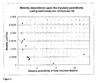
- high quality transistors can be obtained with very low dependence of the mobility on gate field.
- Low permittivity materials lead to lower gate capacitance, reducing the number of induced carriers.
- it has only a linear effect on the drain current and is easily compensated for by the reduction in interface trapping with the potential to increase carrier mobility significantly.
- an organic field effect device manufactured by the process of the first aspect of the invention.
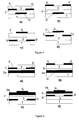
- layer 1 is a substrate
- layer 2 is an insulator
- layer 3 is an organic semiconductor
- S and D are source and drain electrodes
- G is the gate electrode.
- item 2 a is a second insulator layer.
- the invention may comprise depositing at least one high permittivity insulator layer on the other side of the low permittivity insulator layer from the organic semiconductor, to form a further part of the gate insulator.
- the at least one high permittivity insulator layer preferably has a higher permittivity than the low permittivity insulator layer.
- the at least one high permittivity insulator layer has a relative permittivity of 3.5 or higher, more preferably 10 or higher, and most preferably 20 or higher. The highest possible permittivity is preferred.
- the permittivity may range up to about 200.
- the at least one high permittivity insulator layer is also deposited from a solution.
- the organic semiconductor layer and/or the layer(s) of the gate insulator may be deposited from solution by spin coating.
- the whole process of manufacturing the device may be performed at or below about 100°C, thus making the process much less difficult to carry out than prior art manufacturing processes.
- both the organic semiconductor layer and the gate insulator layer(s) are deposited from solution large areas can be coated readily.
- the low permittivity gate insulator layer it has been found that even if the organic semiconductor layer is disordered or semi-ordered good mobilities are achieved.
- the gate insulator layer comprises an organic material, e.g. a polymer.
- an FET structure of Fig.1c is prepared by spin coating the semiconductor onto the substrate with pre-patterned drain and source electrodes. Next, an insulator in the form of a low permittivity polymer of relative permittivity below 3 is spin coated onto the semiconductor followed by the deposition of the gate electrode by vacuum evaporation or liquid deposition of a conductive solution or dispersion. It will be appreciated that the order of process steps may be altered to achieve structures a, b or d shown in Fig.1 . It will be appreciated that the OFET could also have a vertical structure.
- the low permittivity organic insulator should have a conductivity less than 10 -6 Scm -1 to avoid leakage to the gate.
- Preferred insulators are materials of low polarity. It is desirable that the low frequency (measured between 50 to 10,000Hz) permittivity (dielectric constant) ⁇ of the material should be below 3.0, and preferably 1.1 or greater. The permittivity is more preferably in the range 1.3-2.5, and especially in the range 1.5 to 2.1. A further preferred lower limit on the permittivity is 1.7. Such materials have few permanent dipoles, which could otherwise enhance localisation of charges on molecular sites at the interface with the semiconductor.
- the permittivity (dielectric constant) can be determined by the ASTM D150 test method.
- Permittivity values of polymers may be found, for example, in the Handbook of Electrical and Electronic Insulating Materials (The Institute of Electrical and Electronic Engineers Inc., New York, 1995). It is desirable that the permittivity of the material has little dependence of frequency. This is typical of low or non-polar materials. Polymers and copolymers can be chosen by the permittivity of their substituent groups. The low permittivity material may be porous in order to achieve a very low permittivity.
- Preferred low permittivity materials may, for example, be polypropylene, preferably amorphous polypropylene, or low permittivity fluoropolymers, for example copolymers of tetrafluoroethylene and dioxoles such as 2,2 bistrifluoromethyl-4,5-difluoro-1,3-dioxole available, for example from Aldrich or DuPont under the tradename Teflon AF or from Asahi Glass under the tradename CYTOP.
- the latter amorphous copolymers have been successfully used in microelectronics as interlayer insulators, where a low permittivity is required for reducing crosstalk between conductive tracks.
- Suitable materials are low permittivity fluoropolymers, fluoroepoxy polymers, fluorosilane, fluoroacryclic polymers which are available, for example from Cytonix Corporation in the PFC GH, PFC GU, PFC MH product range, and poly(dimethyl)siloxane and its copolymers.
- the polymer may optionally be cross-linked after coating by heat or radiation.
- Table 2 Insulator Typical low frequency permittivity ( ⁇ ) Poly (ethylene/tetrafluoroethylene) 2.6 Poly (ethylene/chlorotrifluoroethylene) 2.3 Fluorinated ethylene/propylene copolymer 2-2.5 Polystyrene-co- ⁇ -methyl styrene 2.5-2.6 Ethylene/ethyl acrylate copolymer 2.8 Poly (styrene/10%butadiene) 2.6 Poly (styrene/15%butadiene), 2.6 Poly (styrene/2,4 dimethylstyrene) 2.5 Cytop 2.0 Teflon AF 1.9-2.1 Polypropylene-co-1-butene 2.2
- a top gate configuration e.g. Fig.1 c,d
- the low permittivity insulator is coated from a solvent which does not dissolve semiconductors typically used in organic FETs.
- Preferred solvents for the deposition of the gate insulator layer are fluorosolvents, preferably perfluorosolvents such as Fluorinert (trade name) FC40, FC75 (mainly consisting of perfluoro cyclic ethers), FC77 (mainly perfluorooctane) which are particularly suitable, resulting in sharp interface layers between the semiconductor and the insulator.
- Typical organic semiconductors such as oligo- and polythiophenes are virtually insoluble in perfluorosolvents.
- a bottom gate configuration e.g. Fig.1a,b
- the amorphous perfluoropolymers provide excellent chemical resistance against aromatic or chloro- solvents used to coat organic semiconductors.
- a further advantage of the low permittivity materials is that they are hydrophopic and will provide a good barrier to water. Highly polar water molecules may introduce undesirable dipolar disorder at the semiconductor interface.
- PVP polyvinylphenol
- the organic semiconductor layer may be deposited before or after the gate insulator layer is deposited.
- the organic field effect transistor device of the invention comprises a further insulator layer, of permittivity higher than the low permittivity layer.
- the organic field effect transistor device of the invention may comprise two or more such further insulator layers.
- the low permittivity gate insulator layer 2 may be used in a thin layer next to the semiconductor and a second insulator layer 2a of higher permittivity next to the first insulator layer.
- the advantage of such configuration is that the first insulator layer of low polarity will screen the random dipole field of the second insulator material from the semiconductor.
- the insulator layer 2 does not have to be much thicker than a few times the size of dipoles found in the second insulator material 2a.
- a practical layer thickness for the first insulator layer 2 may be 5 nm or greater, up to 1 ⁇ m.
- the second insulator layer 2a of high permittivity may be of any thickness, for example 50 nm to 10 ⁇ m. It may be appreciated that further insulator layers can also be employed based on the idea of using a first layer of a thin, low permittivity material in contact with the semiconductor.
- the second layer preferably has a permittivity greater than 3.5 to maximise the gate capacitance.
- the second insulator layer more preferably has a permittivity greater than 10, even more preferably greater than 20, for example between 20 to 200 to maximise the gate capacitance.
- the further insulator layers may optionally be crosslinked.
- Polymers used in this layer may for example be polvinylalcohol, polyvinylphenol, polymethylmethacrylate, cyanoethylated polysaccharides such as cyanoethylpullulane, high permittivity flurorpolymers such as polyvinylidenefluoride, polyurethane polymers and poly(vinyl chloride/vinylacetate) polymers.
- the second insulator layer may be vapour deposited or deposited from solution, and is preferably deposited from solution.
- High permittivity composite materials are particularly useful as the second gate insulator layer, for example composites of TiO2, Ta 2 O 5 SrTiO 3 , Bi 4 Ti 3 O 12 , BaMgF 4 , barium zirconium titanate, barium strontium titanate. These may be deposited preferably by liquid coating in the form of dispersions or by sol-gel processes.
- the combination of a low permittivity layer adjacent the organic semiconductor and further high permittivity layers in a multilayer gate insulator can reduce the operating voltage and at the same time eliminate interface trapping, hysteresis and increase mobility.
- intermediate layers can be deposited between the low and high permittivity layers of a multilayer insulator stack. Such intermediate layers can improve adhesion or wetting between coating steps.
- the intermediate layer for example can be another low permittivity material with different surface properties. Surface treatments, for example plasma treatment, may also be used to improve layer compatibility.
- the organic semiconductor may be an n or p type, and is deposited from solution.
- Preferred organic semiconductors have a FET mobility of greater than 10 -5 cm 2 V -1 s -1 .
- the organic semiconductor may be any conjugated aromatic molecule containing at least three aromatic rings.
- Preferred organic semiconductors contain 5, 6 or 7 membered aromatic rings, especially preferred organic semiconductors contain 5 or 6 membered aromatic rings.
- Each of the aromatic rings may optionally contain one or more hetero atoms selected from Se, Te, P, Si, B, As, N, O or S, preferably from N, O or S.
- the rings may be optionally substituted with alkyl, alkoxy, polyalkoxy, thioalkyl, acyl, aryl or substituted aryl groups, a fluorine atom, a cyano group, a nitro group or an optionally substituted secondary or tertiary alkylamine or arylamine -N(R 3 )(R 4 ), where R 3 and R 4 each independently is H, optionally substituted alkyl, optionally substituted aryl, alkoxy or polyalkoxy groups.
- the alkyl and aryl groups may be optionally fluorinated.
- T 1 and T 2 each independently represent H, Cl, F, -C ⁇ N or lower alkyl groups particularly C 1-4 alkyl groups; R' represents H, optionally substituted alkyl or optionally substituted aryl.
- the alkyl and aryl groups may be optionally fluorinated.
- organic semi-conducting materials that can be used in this invention include compounds, oligomers and derivatives of compounds of the following list : conjugated hydrocarbon polymers such as polyacene, polyphenylene, poly(phenylene vinylene), polyfluorene including oligomers of those conjugated hydrocarbon polymers; condensed aromatic hydrocarbons such as anthracene, tetracene, chrysene, pentacene, pyrene, perylene, coronene; oligomeric para substituted phenylenes such as p-quaterphenyl (p-4P), p-quinquephenyl (p-5P), p-sexiphenyl (p-6P); conjugated heterocyclic polymers such as poly(3-substituted thiophene), poly(3,4-bisubstituted thiophene), polybenzothiophene, polyisothianapthene, poly( N -substituted pyrrol
- a preferred class of semiconductors has repeat units of formula 1: where each Y 1 is independently selected from P, S, As, N and Se and preferably polyarylamines, where Y 1 is N; Ar 1 and Ar 2 are aromatic groups and Ar 3 is present only if Y 1 is N, P, or As in which case it too is an aromatic group.
- Ar 1 , Ar 2 and Ar 3 may be the same or different and represent, independently if in different repeat units, a multivalent (preferably bivalent) aromatic group (preferably mononuclear but optionally polynuclear) optionally substituted by at least one optionally substituted C 1-40 carbyl-derived groups and/or at least one other optional substituent
- Ar 3 represents, independently if in different repeat units, a mono or multivalent (preferably bivalent) aromatic group (preferably mononuclear but optionally polynuclear) optionally substituted by at least one: optionally substituted C 1-40 carbyl-derived group and/or at least one other optional substituent; where at least one terminal group is attached in the polymer to the Ar 1 , Ar 2 and optionally Ar 3 groups located at the end of the polymer chains, so as to cap the polymer chains and prevent further polymer growth, and at least one terminal group is derived from at least one end capping reagent used in the polymerisation to form said polymeric material to control the molecular weight thereof.
- WO 99/32537 and WO 00/78843 are patent applications of the applicants, which describes certain novel oligomers and polymers, which have repeat units of formula 1. The disclosures of these applications are incorporated herein by reference, as these materials are particularly useful as semiconductors in the present invention.
- the number average degree of polymerisation is denoted by n and the number of the repeat units of Formula 1 which may be present per molecule in the invention may be from 2 to 1,000, preferably 3 to 100 and more preferably 3 to 20 inclusive.
- the polymer may comprise a mixture of different polymeric species of varying chain lengths and with a distribution of molecular weights (polydisperse) or consist of molecules of a single molecular weight (monodisperse).
- the preferred polymeric materials are obtainable by polymerisation controlled by the addition of at least one end capping reagent in an amount sufficient to reduce substantially further growth of the polymer chain.
- the invention also relates to polymers further substituted with, on average, more than one aryl moiety which is further substituted with a moiety capable of chain extension or cross linking, for example by photopolymerisation or by thermal polymerisation.
- moieties capable of chain extension are preferably hydroxy, glycidyl ether, acrylate ester, epoxide, methacrylate ester, ethenyl, ethynyl, vinylbenzyloxy, maleimide, nadimide, trifluorovinyl ether, a cyclobutene bound to adjacent carbons on an aryl moiety or a trialkylsiloxy.
- amine materials that may be useful in this invention are tetrakis(N,N'-aryl)biaryldiamines, bis(N,N'-[substituted]phenyl) bis(N,N'-phenyl)-1,1-biphenyl-4,4'-diamines including 4-methyl, 2,4-dimethyl and/or 3-methyl derivatives thereof, tetrakis(N,N-aryl)biphenyl-4,4'-diamine-1,1-cyclohexanes and their derivatives, triphenylamine and its alkyl and aryl derivatives and poly(N-phenyl-1,4-phenyleneamine), N-dibenzo[a,d]cycloheptene-5-ylidene-N',N'-di- p -tolyl-benzene-1,4-diamine, (9,9-dimethyl-9H-fluorene-2-yl)-di- p -to
- These molecules may be prepared directly via a multi-stage chemical synthesis which produces each molecule in a chemically pure monodisperse form.
- Conjugated oligomeric and polymeric heterocyclic semiconductors may comprise a repeat unit of an optionally substituted 5 membered ring and terminal groups A 1 and A 2 as shown in Formula 2: in which X may be Se, Te or preferably O, S, or -N(R)- where R represents H, optionally substituted alkyl or optionally substituted aryl; R 1 , R 2 , A 1 and A 2 may be independently H, alkyl, alkoxy, thioalkyl, acyl, aryl or substituted aryl, a fluorine atom, a cyano group, a nitro group or an optionally substituted secondary or tertiary alkylamine or arylamine -N(R 3 )(R 4 ), where R 3 and R 4 are as defined above.
- the alkyl and aryl groups represented by R 1 , R 2 , R 3 , R 4 , A 1 and A 2 may be optionally fluorinated.
- the number of recurring units in the conjugated oligomer of Formula 2 is represented by an integer n , n is defined as for Formula 1. In compounds of Formula 2 n is preferably 2 to 14.
- Oligomers containing a conjugated linking group may be represented by Formula 3: in which X may be Se, Te, or preferably O, S, or -N(R)-, R is as defined above; R 1 , R 2 , A 1 and A 2 as defined above for Formula 2.
- Polymers may have repeat units of the general Formula 4: in which X, R 1 and R 2 are defined as above.
- the sub units may be polymerised in such a way as to give a regio regular or a regio random polymer comprising repeat units as shown in Formulae 4 to 6:
- Polymers may have repeat units of the general Formula 7: in which X is as defined above and the bridging group A is optionally fluorinated C 1-6 alkyl, for example poly(3,4-ethylenedioxy)thiophene-2,5-diyl and poly(3,4-trimethyldioxy) thiophene-2,5-diyl.
- Polymers may have repeat units of general Formula 8: in which X, R 1 and R 2 are defined as above. Specific examples are where one of R 1 or R 2 is an alkoxide of general formula C n H 2n+1 O-, and the other of R 1 or R 2 is H, poly(dodecyloxy- ⁇ , ⁇ ',- ⁇ , ⁇ " terthienyl) i.e. polyDOT 3 .
- Polymers may have repeat units of general Formula 9: in which X is as defined above; R 5 and R 6 may be independently H, alkyl, aryl or substituted aryl. The alkyl and aryl groups may be optionally fluorinated.
- Polymers may have repeat units of general Formula 10: in which R 7 and R 8 are each independently optionally substituted C 1-20 hydrocarbyl, C 4-16 hydrocarbyl carbonyloxy, C 4-16 aryl(trialkylsiloxy) or both R 7 and R 8 may form with the 9-carbon on the fluorene ring a C 5-20 ring structure or a C 4-20 ring structure containing one or more heteroatoms of S, N or O.
- Polymers may have repeat units of general Formula 11: wherein R 9 is C 1-20 hydrocarbyl optionally substituted with di(C 1-20 alkyl)amino, C 1-20 hydrocarbyloxy or C 1-20 hydrocarbyl or tri(C 1-10 alkyl)siloxy.
- Copolymers comprising repeat units as described above and also other repeat units comprising two or more of the repeat units could be used.
- Copolymers preferably comprise one or more repeat units of Formula 10 or Formula 11 and Formula 1.
- copolymers comprise one or more repeat units of Formula 1 and one or more repeat units of at least one of Formulae 2 to 9.
- Preferred copolymers for use in the semiconductor layer include oligomers or polymers containing fluorene copolymerised with an arylamine or copolymerised with a thiophene.
- the semiconductor is a p type semiconductor this is preferably a monodisperse polyarylamine, mixtures of monodisperse polyarylamines, fluorine arylamine co-polymers, or cross-linkable arylamines.
- the semiconductor is an n type semiconductor this is preferably a fluorophthalocyanines, or a substituted diaryl-1,4,5,8-naphthalenetetracarboxylic diimide and its oligomers.
- the semiconducting channel may also be a composite of two or more of the same types of semiconductors.
- a p type channel material may, for example be mixed with n-type materials for the effect of doping the layer.
- Multilayer semiconductor layers may also be used.
- the semiconductor may be intrinsic near the insulator interface and a highly doped region can additionally be coated next to the intrinsic layer.
- a test field effect transistor was manufactured by using a Melinex substrate upon which were patterned Pt/Pd source and drain electrodes by standard techniques, e.g. shadow masking.
- the semiconductor was dissolved one part into 99 parts of solvent, typically toluene, and spin coated onto the substrate at 1000 rpm for 20 s to yield a ⁇ 100 nm film.
- solvent typically toluene
- a solution of the insulator material was then spin-coated onto the semiconductor giving a thickness typically in the range 0.5 ⁇ m to 1 ⁇ m.
- the sample was placed once more in an oven at 100 °C to evaporate solvent from the insulator.
- a gold gate contact was defined over the device channel area by evaporation through a shadow mask.
- a number of devices were prepared which consisted of a non-patterned Pt/Pd base layer, an insulator layer prepared in the same way as that on the FET device, and a top electrode of known geometry. The capacitance was measured using a hand-held multimeter, connected to the metal either side of the insulator.
- the voltages applied to the transistor are relative to the potential of the source electrode.
- a negative potential is applied to the gate
- positive charge carriers are accumulated in the semiconductor on the other side of the gate insulator.
- This is called the accumulation mode.
- the capacitance/area of the gate insulator C ⁇ determines the amount of the charge thus induced.
- V DS negative potential
- the accumulated carriers yield a source-drain current I DS which depends primarily on the density of accumulated carriers and, importantly, their mobility in the source-drain channel. Geometric factors such as the drain and source electrode configuration, size and distance also affect the current.
- I DS ⁇ ⁇ WC i L ⁇ V G - V 0 ⁇ V DS - V DS 2 2 + I ⁇ , where V 0 is an offset voltage and I ⁇ is an ohmic current independent of the gate voltage and is due to the finite conductivity of the material.
- V 0 is an offset voltage
- I ⁇ is an ohmic current independent of the gate voltage and is due to the finite conductivity of the material.
- the transistor sample was mounted in a sample holder. Microprobe connections were made to the gate, drain and source electrodes using Karl Suss PH100 miniature probe-heads. These were linked to a Hewlett-Packard 4155B parameter analyser. The drain voltage was set to -20 V and the gate voltage was scanned from +20 to -40 V in 1 V steps. When
- the field effect mobility can be calculated from the gradient of I DS vs. V G given by equation 2.
- S ⁇ ⁇ WC i ⁇ V DS L
- OFETs were prepared using organic semiconductor of Formula 12 (Example 5) and Formula 13 (Example 6).
- a low permittivity perfluoropolymer, Cytop107M (Asahi Glass, Z-1700E01) was used to form the gate insulator.
- the insulator was spin coated from a 1:1 mixture with FC75 solvent (Acros 12380-0100).
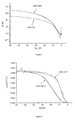
- the devices yielded very low hysteresis and threshold voltage.
- the mobility did not vary with applied gate bias when V G was more negative than V D .
- the mobilities obtained are shown in Table 1, together with all the mobilities obtained in the following examples.
- An OFET was prepared using OSC of Formula 13.
- a low permittivity perfluoropolymer, Teflon AF1600 (Aldrich, 46,961-0) was used to form the gate insulator.
- the insulator was spin coated from a 25:1 mixture with FC40 solvent (Acros 12376-0100). The device yielded very low hysteresis and threshold voltage. In addition the mobility did not vary with applied gate bias when V G was more negative than V D .
- An OFET was prepared using OSC of Formula 14.
- a prior art polar polymer, polymethylmethacrylate (Aldrich 18,226-5) was used to form the gate insulator.
- the insulator was spin coated from a 12.5:1 mixture with acetone. The device exhibited hysteresis and a dependence of the mobility upon applied gate bias.
- An OFET was prepared using an OSC of Formula 14.
- a prior art polar polymer, poly-4-vinyl-phenol (Aldrich 43,622-4) was used to form the gate insulator.
- the insulator was spin coated from a 10:1 (w/w) solution in methanol. The device exhibited hysteresis and a dependence of the mobility upon applied gate bias.
- An OFET was prepared using OSC of Formula 14 on predefined source and drain electrodes on a thermally oxidised silicon substrate as described in PCT/GB01/05145 .
- the 200 nm SiO 2 layer served as the gate insulator.
- Such SiO 2 gate insulators are widely used in the prior art.
- the device exhibited hysteresis and a strong dependence of the mobility upon applied gate bias.
- An OFET was prepared using an OSC of Formula 14.
- the insulator was spin coated from a 10% (w/w) solution in acetone.
- the device exhibited very strong hysteresis and a significant dependence of the mobility upon applied gate bias.
- the difference in threshold voltage between scanning the voltage on the gate in the direction +20V to -40V compared with -40V to +20V was approximately 5V.
- Example 13 An OFET was prepared and tested as described in Example 13 except the OSC layer was washed with acetone prior depositing the insulator. By washing off any semiconductor polymer fraction that may be soluble in acetone we aimed at reducing intermixing between the OSC layer and the CYMM insulator layer. However, this has not improved the mobility compared to Example 13.
- An OFET was prepared using an OSC of Formula 14.
- a low permittivity polymer polyisobutylene (PIB) (Aldrich, 18,145-5) was used to form the gate insulator.
- the insulator was spin coated from a 3% (w/w) solution in hexane. The device yielded very low hysteresis and threshold voltage.
- An OFET was prepared using an OSC of Formula 13.
- a low permittivity polymer polyisobutylene (PIB) (Aldrich, 18,145-5) was used to form the gate insulator.
- the insulator was spin coated from a 3% (w/w) solution in hexane. The device yielded very low hysteresis and threshold voltage.
- An OFET was using an OSC of Formula 14.
- a low permittivity polymer polyisobutyl-methacrylate (PIBMMA) (Aldrich, 44,576-2) was used to form the gate insulator.
- the insulator was spin coated from a 10% (w/w) solution in isopropanol. The device yielded very low hysteresis and threshold voltage.
- An OFET was prepared using an OSC of Formula 14.
- a polar polymer, poly(4-vinylphenol-co-methyl methacrylate) (PVPMMA) (Aldrich, 47,457-6) was used to form the gate insulator.
- the insulator was spin coated from a 15% (w/w) solution in ethanol.
- An OFET was prepared using an OSC of Formula 14.
- a low permittivity perfluoropolymer, Teflon AF2400 (Aldrich, 46,962-9) was used to form the gate insulator.
- the insulator was spin coated from a 1.5%(w/w) mixture with FC75 solvent. The device yielded very low hysteresis and threshold voltage.
- An OFET was prepared using OSC of Formula 14.
- the polymer polyvinylchloride (PVC) Aldrich, 18,958-8-8 was used to form the gate insulator.
- the insulator was spin coated from a 2.5% (w/w) solution in tetrachloroethane onto an aluminised piece of mylar to form a bottom gate structure.
- the OSC (of formula 14) was spin coated on top of the insulator and source-drain electrodes were deposited by the thermal evaporation of gold through a shadow mask on top of the OSC.
- An OFET was prepared using an OSC of Formula 14 mixed with a binder polymer poly(alpha-methylstyrene) (Aldrich, 19,184-1) at 3:1 ratio (w/w).
- a low permittivity perfluoropolymer, Cytop809A (Asahi Glass) was used to form the gate insulator.
- the insulator was spin coated from a 1:1 mixture (w/w) with FC75 solvent. The device yielded very low hysteresis and threshold voltage.
- An OFET was prepared with the same semiconductor/binder layer as in Example 20, but using prior art SiO2 as the insulator, as described in Example 10.
- the semiconductor yielded lower mobility and stronger hysteresis than in Example 20.
- the device exhibited hysteresis and a dependence of the mobility upon applied gate bias.
- An OFET was prepared and tested as described in Example 3 using OSC of Formula 14.
- a low permittivity fluoropolymer, CYTONIX PFC2050 (Cytonix corp.) was used to form the gate insulator.
- the insulator was spin coated from a 14% (w/w) solution using FC75 as a solvent. The device yielded very low hysteresis and threshold voltage.
- An OFET was prepared using an OSC of Formula 14.
- a high permittivity polymer poly vinyl alcohol (Aldrich, 36,316-2) was used to form the gate insulator.
- the insulator was spin coated from a 4% (w/w) solution in water. The device exhibited hysteresis and a dependence of the mobility upon applied gate bias.
- An OFET was prepared and tested as described in Example 3 using OSC of Formula 14.
- a low permittivity polymer poly (propylene-co-1-butene) (Aldrich 43,108-7) was used to form the gate insulator.
- the insulator was spin coated from a 2% (w/w) solution in cyclohexane (warmed to dissolve polymer). The device yielded very low hysteresis and threshold voltage.
- OFETs were prepared using organic semiconductor of Formula 15.
- a low permittivity perfluoropolymer, Cytop107M (Asahi Glass, Z-1700E01) was used to form the gate insulator.
- the insulator was spin coated from a 1:1 mixture with FC75 solvent (Acros 12380-0100). The devices yielded very low hysteresis and threshold voltage.
- An OFET was prepared using OSC of Formula 15.
- a prior art polar polymer, polymethylmethacrylate (Aldrich 18,226-5) was used to form the gate insulator.
- the insulator was spin coated from a 12.5:1 mixture with acetone. The device exhibited hysteresis and a dependence of the mobility upon applied gate bias.
- An OFET was prepared using an OSC of Formula 14. Three dielectric layers were used to form the gate insulator.
- the first layer (adjacent to the OSC) was a low permittivity perfluoropolymer, Cytop107M (Asahi Glass, Z-1700E01). This was spin coated from a 1:1 mixture with FC75 solvent.
- the second layer polyisobutylene (PIB) (Aldrich, 18,145-5), was spin coated from a 3% (w/w) solution in hexane.
- An OFET was prepared using an OSC of Formula 13 in anisole. Two dielectric layers were used to form the gate insulator. The first layer (adjacent to the OSC) was a low permittivity polymer polyisobutylene (PIB) (Aldrich, 18,145-5), spun from a 3% (w/w) solution in hexane. The second layer, polycyanopulluane (CYMM) (ShinEtsu), was spin coated from a 10% (w/w) solution in acetone. The device yielded very low hysteresis and threshold voltage but achieved a much higher on current than using the PIB alone due to the higher overall capacitance of the PIB/CYMM stack.
- PIB low permittivity polymer polyisobutylene
- CYMM polycyanopulluane
- An OFET was prepared using an OSC of Formula 13. Two dielectric layers were used to form the gate insulator. The first layer (adjacent to the OSC) was a low permittivity polymer polypropylene (Aldrich, 42,818-3) spun from a 1% (w/w) solution in hexane. The second layer, polycyanopulluane (CYMM) (ShinEtsu), was spin coated from a 10% (w/w) solution in acetone.
- CYMM polycyanopulluane
- An OFET was prepared using an OSC of Formula 14. Two dielectric layers were used to form the gate insulator. The first layer (adjacent to the OSC) was a low permittivity perfluoropolymer, Cytop107M (Asahi Glass, Z-1700E01). This was spin coated from a 1% (w/w) solution in FC75 solvent. The sample was subjected to an air plasma for 5 minutes to make the surface more hydrophilic. The second layer, polycyanopulluane (CYMM) (ShinEtsu), was spin coated from a 10% (w/w) solution in acetone. The device yielded very low hysteresis and threshold voltage.
- CYMM polycyanopulluane
- An OFET was prepared using an OSC of Formula 14. Three dielectric layers were used to form the gate insulator.
- the first layer (adjacent to the OSC) was a low permittivity perfluoropolymer, Cytop107M (Asahi Glass, Z-1700E01). This was spin coated from a 1:1 mixture with FC75 solvent.
- the second layer polypropylene (PP) (Aldrich, 42,818-3), was spin coated from a saturated solution in toluene.
- the third layer, poly vinylidine fluoride (PVDF) (Aldrich 42,715-2), was spin coated from a 5% (w/w) solution in NMP (N-Methylpyrrolidone). The device yielded very low hysteresis and threshold voltage.
- An OFET was prepared using an OSC of Formula 14. Three dielectric layers were used to form the gate insulator.
- the first layer (adjacent to the OSC) was a low permittivity perfluoropolymer, Teflon AF1600 (Aldrich, 46,961-0). This was spin coated from a 3% (w/w) solution in FC75 solvent.
- the second layer polypropylene (PP) (Aldrich, 42,818-3), was spin coated from a saturated solution in toluene.
- the third layer, poly vinylidine fluoride (PVDF) (Aldrich 42,715-2), was spin coated from a 5% (w/w) solution in NMP. The device yielded very low hysteresis and threshold voltage.
Landscapes
- Engineering & Computer Science (AREA)
- Chemical & Material Sciences (AREA)
- Manufacturing & Machinery (AREA)
- Organic Chemistry (AREA)
- Physics & Mathematics (AREA)
- Computer Hardware Design (AREA)
- Microelectronics & Electronic Packaging (AREA)
- Power Engineering (AREA)
- Condensed Matter Physics & Semiconductors (AREA)
- General Physics & Mathematics (AREA)
- Inorganic Chemistry (AREA)
- Thin Film Transistor (AREA)
- Formation Of Insulating Films (AREA)
- Electroluminescent Light Sources (AREA)
- Liquid Deposition Of Substances Of Which Semiconductor Devices Are Composed (AREA)
- Electrodes Of Semiconductors (AREA)
Applications Claiming Priority (4)
| Application Number | Priority Date | Filing Date | Title |
|---|---|---|---|
| GB0130321A GB0130321D0 (en) | 2001-12-19 | 2001-12-19 | Electronic devices |
| GB0130451A GB0130451D0 (en) | 2001-12-20 | 2001-12-20 | Electronic devices |
| GB0220504A GB0220504D0 (en) | 2002-09-03 | 2002-09-03 | Electronic devices |
| EP02779719A EP1459392B1 (en) | 2001-12-19 | 2002-11-21 | Organic field effect transistor with an organic dielectric |
Related Parent Applications (1)
| Application Number | Title | Priority Date | Filing Date |
|---|---|---|---|
| EP02779719.0 Division | 2002-11-21 |
Publications (1)
| Publication Number | Publication Date |
|---|---|
| EP2204861A1 true EP2204861A1 (en) | 2010-07-07 |
Family
ID=27256358
Family Applications (3)
| Application Number | Title | Priority Date | Filing Date |
|---|---|---|---|
| EP10004331A Withdrawn EP2204861A1 (en) | 2001-12-19 | 2002-11-21 | Organic field effect transistor with an organic dielectric |
| EP10004332A Withdrawn EP2207217A1 (en) | 2001-12-19 | 2002-11-21 | Organic field effect transistor with an organic dielectric |
| EP02779719A Expired - Lifetime EP1459392B1 (en) | 2001-12-19 | 2002-11-21 | Organic field effect transistor with an organic dielectric |
Family Applications After (2)
| Application Number | Title | Priority Date | Filing Date |
|---|---|---|---|
| EP10004332A Withdrawn EP2207217A1 (en) | 2001-12-19 | 2002-11-21 | Organic field effect transistor with an organic dielectric |
| EP02779719A Expired - Lifetime EP1459392B1 (en) | 2001-12-19 | 2002-11-21 | Organic field effect transistor with an organic dielectric |
Country Status (9)
Cited By (1)
| Publication number | Priority date | Publication date | Assignee | Title |
|---|---|---|---|---|
| CN105404046A (zh) * | 2015-12-04 | 2016-03-16 | 深圳市华星光电技术有限公司 | 量子点彩膜基板的制作方法 |
Families Citing this family (175)
| Publication number | Priority date | Publication date | Assignee | Title |
|---|---|---|---|---|
| JP2004241528A (ja) * | 2003-02-05 | 2004-08-26 | Ricoh Co Ltd | 有機半導体装置及びそれを有する表示素子 |
| US6950299B2 (en) | 2003-02-13 | 2005-09-27 | Plastic Logic Limited | Non-linear capacitors |
| GB0303267D0 (en) * | 2003-02-13 | 2003-03-19 | Plastic Logic Ltd | Non lineur capacitors |
| KR100726114B1 (ko) * | 2003-06-27 | 2007-06-12 | 티디케이가부시기가이샤 | 전계 효과 트랜지스터 |
| KR100995451B1 (ko) * | 2003-07-03 | 2010-11-18 | 삼성전자주식회사 | 다층 구조의 게이트 절연막을 포함하는 유기 박막 트랜지스터 |
| JP4325479B2 (ja) * | 2003-07-17 | 2009-09-02 | セイコーエプソン株式会社 | 有機トランジスタの製造方法、アクティブマトリクス装置の製造方法、表示装置の製造方法および電子機器の製造方法 |
| JP2005072569A (ja) * | 2003-08-06 | 2005-03-17 | Mitsubishi Chemicals Corp | 有機電界効果トランジスタ |
| GB0318817D0 (en) * | 2003-08-11 | 2003-09-10 | Univ Cambridge Tech | Method of making a polymer device |
| DE10340608A1 (de) * | 2003-08-29 | 2005-03-24 | Infineon Technologies Ag | Polymerformulierung und Verfahren zur Herstellung einer Dielektrikumsschicht |
| JP2005079549A (ja) * | 2003-09-03 | 2005-03-24 | Victor Co Of Japan Ltd | 有機薄膜トランジスタ |
| JP2005136383A (ja) * | 2003-10-09 | 2005-05-26 | Canon Inc | 有機半導体素子、その製造方法および有機半導体装置 |
| US8450723B2 (en) | 2003-11-04 | 2013-05-28 | Alcatel Lucent | Apparatus having an aromatic dielectric and an aromatic organic semiconductor including an alkyl chain |
| EP1808866A1 (en) | 2003-11-28 | 2007-07-18 | Merck Patent GmbH | Organic semiconducting layer formulations comprising polyacenes and organic binder polymers |
| JP2005175386A (ja) * | 2003-12-15 | 2005-06-30 | Asahi Kasei Corp | 有機半導体素子 |
| JP2005191437A (ja) * | 2003-12-26 | 2005-07-14 | Ricoh Co Ltd | 半導体装置、その製造方法、および表示装置 |
| GB0400997D0 (en) | 2004-01-16 | 2004-02-18 | Univ Cambridge Tech | N-channel transistor |
| US7256436B2 (en) | 2004-03-30 | 2007-08-14 | Shin-Etsu Chemical Co., Ltd. | Thin-film field-effect transistors and making method |
| JP4449549B2 (ja) * | 2004-04-15 | 2010-04-14 | 日本電気株式会社 | 有橋環式炭化水素ラクトン構造を有する材料を用いた有機薄膜トランジスタとその製造方法 |
| US7372070B2 (en) * | 2004-05-12 | 2008-05-13 | Matsushita Electric Industrial Co., Ltd. | Organic field effect transistor and method of manufacturing the same |
| KR100560796B1 (ko) | 2004-06-24 | 2006-03-13 | 삼성에스디아이 주식회사 | 유기 박막트랜지스터 및 그의 제조방법 |
| KR100635567B1 (ko) * | 2004-06-29 | 2006-10-17 | 삼성에스디아이 주식회사 | 박막트랜지스터 및 그 제조 방법 |
| EP1648040B1 (en) * | 2004-08-31 | 2016-06-01 | Osaka University | Thin-layer chemical transistors and their manufacture |
| GB2418062A (en) | 2004-09-03 | 2006-03-15 | Seiko Epson Corp | An organic Field-Effect Transistor with a charge transfer injection layer |
| JP2008513544A (ja) * | 2004-09-14 | 2008-05-01 | ノースウェスタン ユニバーシティ | カルボニル官能化チオフェン化合物および関連する装置構造 |
| JP4502382B2 (ja) * | 2004-11-02 | 2010-07-14 | キヤノン株式会社 | 有機トランジスタ |
| KR100669752B1 (ko) | 2004-11-10 | 2007-01-16 | 삼성에스디아이 주식회사 | 유기 박막 트랜지스터, 이의 제조 방법 및 이를 구비한평판표시장치 |
| KR101122231B1 (ko) * | 2004-12-17 | 2012-03-19 | 삼성전자주식회사 | 유기 반도체를 이용한 박막 트랜지스터 표시판 및 그 제조방법 |
| KR101142998B1 (ko) | 2004-12-20 | 2012-05-08 | 재단법인서울대학교산학협력재단 | 유기 절연막 및 유기 절연막을 포함하는 박막 트랜지스터표시판 및 그 제조 방법 |
| EP1839339A2 (en) | 2004-12-23 | 2007-10-03 | Northwestern University | Siloxane-polymer dielectric compositions and related organic field-effect transistors |
| KR101086159B1 (ko) * | 2005-01-07 | 2011-11-25 | 삼성전자주식회사 | 불소계 고분자 박막을 포함하는 유기 박막 트랜지스터 |
| EP1854159A1 (en) | 2005-02-18 | 2007-11-14 | Koninklijke Philips Electronics N.V. | Electronic device |
| JP2006229053A (ja) * | 2005-02-18 | 2006-08-31 | Ricoh Co Ltd | 有機半導体層を有する電界効果型有機薄膜トランジスタ |
| US7619242B2 (en) * | 2005-02-25 | 2009-11-17 | Xerox Corporation | Celluloses and devices thereof |
| JP4450214B2 (ja) * | 2005-03-11 | 2010-04-14 | セイコーエプソン株式会社 | 有機薄膜トランジスタ、電子デバイスおよび電子機器 |
| JP4951868B2 (ja) * | 2005-03-18 | 2012-06-13 | 凸版印刷株式会社 | 薄膜トランジスタの製造方法 |
| EP2259354A3 (en) * | 2005-03-23 | 2011-03-16 | Türkiye Sise Ve Cam Fabrikalari A.S. | Perylene imide/diimide based organic field effect transistors-OFETs and a method of producing the same |
| JP2006269599A (ja) * | 2005-03-23 | 2006-10-05 | Sony Corp | パターン形成方法、有機電界効果型トランジスタの製造方法、及び、フレキシブルプリント回路板の製造方法 |
| US20060214154A1 (en) * | 2005-03-24 | 2006-09-28 | Eastman Kodak Company | Polymeric gate dielectrics for organic thin film transistors and methods of making the same |
| US20060231829A1 (en) * | 2005-04-13 | 2006-10-19 | Xerox Corporation | TFT gate dielectric with crosslinked polymer |
| US20060231908A1 (en) * | 2005-04-13 | 2006-10-19 | Xerox Corporation | Multilayer gate dielectric |
| EP1986247A1 (en) | 2005-05-12 | 2008-10-29 | MERCK PATENT GmbH | Polyacene and semiconductor Formulation |
| TW200703664A (en) * | 2005-05-31 | 2007-01-16 | Nat University Iwate Univ Inc | Organic thin film transistor |
| JP2009501927A (ja) | 2005-07-19 | 2009-01-22 | コーニンクレッカ フィリップス エレクトロニクス エヌ ヴィ | 流体分析装置 |
| KR101209046B1 (ko) * | 2005-07-27 | 2012-12-06 | 삼성디스플레이 주식회사 | 박막트랜지스터 기판과 박막트랜지스터 기판의 제조방법 |
| US7781757B2 (en) | 2005-08-24 | 2010-08-24 | Sanyo Electric Co., Ltd. | Organic semiconductor material, organic semiconductor element and field effect transistor using the same |
| TWI261361B (en) * | 2005-08-31 | 2006-09-01 | Ind Tech Res Inst | Organic thin-film transistor structure and method for fabricating the same is provided |
| US20080113520A1 (en) * | 2005-09-07 | 2008-05-15 | University Of Seoul Foundation Of Industry- Academic Cooperation | Method of Forming Organic Layer on Semiconductor Substrate |
| US7488834B2 (en) | 2005-09-30 | 2009-02-10 | Alcatel-Lucent Usa Inc. | Organic semiconductors |
| US20070075308A1 (en) | 2005-09-30 | 2007-04-05 | Florian Dotz | Active semiconductor devices |
| US7569415B2 (en) | 2005-09-30 | 2009-08-04 | Alcatel-Lucent Usa Inc. | Liquid phase fabrication of active devices including organic semiconductors |
| CN100511751C (zh) * | 2005-10-17 | 2009-07-08 | 中国科学院化学研究所 | 一种有机场效应晶体管及其制备方法 |
| KR100708720B1 (ko) * | 2005-10-19 | 2007-04-17 | 삼성에스디아이 주식회사 | 유기 박막 트랜지스터, 이의 제조 방법 및 이를 구비한평판 표시 장치 |
| DE102005059608B4 (de) * | 2005-12-12 | 2009-04-02 | Polyic Gmbh & Co. Kg | Organisches elektronisches Bauelement mit verbesserter Spannungsstabilität und Verfahren zur Herstellung dazu |
| KR101213871B1 (ko) * | 2005-12-15 | 2012-12-18 | 엘지디스플레이 주식회사 | 박막 트랜지스터 어레이 기판 및 그 제조 방법 |
| US7425723B2 (en) * | 2005-12-21 | 2008-09-16 | Xerox Corporation | Organic thin-film transistors |
| US7514710B2 (en) * | 2005-12-28 | 2009-04-07 | 3M Innovative Properties Company | Bottom gate thin film transistors |
| DE102006055067B4 (de) | 2005-12-29 | 2017-04-20 | Lg Display Co., Ltd. | Organische Dünnfilmtransistoren und Verfahren zu deren Herstellung |
| KR101225372B1 (ko) * | 2005-12-29 | 2013-01-22 | 엘지디스플레이 주식회사 | 박막트랜지스터 및 그 제조방법과 그 박막트랜지스터를포함하는 평판 표시 장치 |
| CN101361205B (zh) | 2006-01-21 | 2012-10-03 | 默克专利股份有限公司 | 包含有机半导体配方的电子短沟道器件 |
| WO2007097165A1 (ja) * | 2006-02-27 | 2007-08-30 | Murata Manufacturing Co., Ltd. | 電界効果トランジスタ |
| TW200737520A (en) * | 2006-03-17 | 2007-10-01 | Univ Nat Chiao Tung | Gate dielectric structure and an organic thin film transistor based thereon |
| GB2453457B (en) | 2006-05-12 | 2011-06-01 | Merck Patent Gmbh | Indenofluorene polymer based organic semiconductor materials |
| JP2007311377A (ja) * | 2006-05-16 | 2007-11-29 | Sony Corp | 薄膜トランジスタの製造方法および薄膜トランジスタならびに表示装置 |
| JP2007318025A (ja) * | 2006-05-29 | 2007-12-06 | Dainippon Printing Co Ltd | 有機半導体素子、および、有機半導体素子の製造方法 |
| JP5256583B2 (ja) * | 2006-05-29 | 2013-08-07 | 大日本印刷株式会社 | 有機半導体素子、および、有機半導体素子の製造方法 |
| US7919825B2 (en) * | 2006-06-02 | 2011-04-05 | Air Products And Chemicals, Inc. | Thin film transistors with poly(arylene ether) polymers as gate dielectrics and passivation layers |
| WO2008002660A2 (en) * | 2006-06-28 | 2008-01-03 | Northwestern University | Crosslinked polymeric dielectric materials and methods of manufacturing and use thereof |
| US8308886B2 (en) | 2006-07-17 | 2012-11-13 | E I Du Pont De Nemours And Company | Donor elements and processes for thermal transfer of nanoparticle layers |
| US7528448B2 (en) | 2006-07-17 | 2009-05-05 | E.I. Du Pont De Nemours And Company | Thin film transistor comprising novel conductor and dielectric compositions |
| US8062824B2 (en) | 2006-07-17 | 2011-11-22 | E. I. Du Pont De Nemours And Company | Thermally imageable dielectric layers, thermal transfer donors and receivers |
| EP2044139B1 (en) | 2006-07-21 | 2011-12-21 | Merck Patent GmbH | Copolymers of indenofluorene and thiophene |
| US20080224127A1 (en) * | 2006-08-22 | 2008-09-18 | Marks Tobin J | Gate dielectric structures, organic semiconductors, thin film transistors and related methods |
| KR100794720B1 (ko) | 2006-08-28 | 2008-01-21 | 경희대학교 산학협력단 | 유기 박막 트랜지스터 표시판 및 그 제조 방법 |
| TW200830595A (en) * | 2006-11-27 | 2008-07-16 | Nat University Iwate Univ Inc | Organic thin film transistor, organic composite electronic element, method for manufacturing such transistor and element, and display device and memory |
| ES2525040T3 (es) * | 2006-11-28 | 2014-12-16 | Polyera Corporation | Materiales dieléctricos basados en fotopolímero y métodos de preparación y uso de los mismos |
| EP1936712A1 (en) * | 2006-12-23 | 2008-06-25 | ETH Zürich | Organic field-effect transistors with polymeric gate dielectric and method for making same |
| TWI323034B (en) * | 2006-12-25 | 2010-04-01 | Ind Tech Res Inst | Electronic devices with hybrid high-k dielectric and fabrication methods thereof |
| JP5234533B2 (ja) * | 2007-03-26 | 2013-07-10 | 国立大学法人九州大学 | 有機半導体素子およびその製造方法 |
| US8637343B2 (en) * | 2007-04-25 | 2014-01-28 | Merck Patent Gmbh | Process for preparing an electronic device |
| GB0709093D0 (en) * | 2007-05-11 | 2007-06-20 | Plastic Logic Ltd | Electronic device incorporating parylene within a dielectric bilayer |
| GB2450382B (en) * | 2007-06-22 | 2009-09-09 | Cambridge Display Tech Ltd | Organic thin film transistors, organic light-emissive devices and organic light-emissive displays |
| WO2009013291A2 (en) * | 2007-07-25 | 2009-01-29 | Basf Se | Field effect elements |
| FR2919521B1 (fr) * | 2007-08-01 | 2012-03-09 | Commissariat Energie Atomique | Couche d'accroche sur des polymeres fluores |
| TWI345671B (en) * | 2007-08-10 | 2011-07-21 | Au Optronics Corp | Thin film transistor, pixel structure and liquid crystal display panel |
| KR20090065254A (ko) * | 2007-12-17 | 2009-06-22 | 한국전자통신연구원 | 광반응성 유기고분자 게이트 절연막 조성물 및 이를 이용한유기 박막 트랜지스터 |
| US7994495B2 (en) * | 2008-01-16 | 2011-08-09 | Xerox Corporation | Organic thin film transistors |
| JP2009224689A (ja) * | 2008-03-18 | 2009-10-01 | Sanyo Electric Co Ltd | 有機トランジスタ及びその製造方法 |
| PT103999B (pt) * | 2008-03-20 | 2012-11-16 | Univ Nova De Lisboa | Processo de utilização e criação de papel à base de fibras celulósicas naturais, fibras sintéticas ou mistas como suporte físico e meio armazenador de cargas elétricas em transístores de efeito de campo com memória autossustentáveis usando óxidos sem |
| GB2458940B (en) | 2008-04-03 | 2010-10-06 | Cambridge Display Tech Ltd | Organic thin film transistors |
| KR101581065B1 (ko) * | 2008-04-24 | 2015-12-29 | 메르크 파텐트 게엠베하 | 전자 디바이스 |
| FR2934714B1 (fr) * | 2008-07-31 | 2010-12-17 | Commissariat Energie Atomique | Transistor organique et procede de fabrication d'une couche dielectrique d'un tel transistor. |
| GB2467316B (en) | 2009-01-28 | 2014-04-09 | Pragmatic Printing Ltd | Electronic devices, circuits and their manufacture |
| WO2010020329A1 (en) | 2008-08-18 | 2010-02-25 | Merck Patent Gmbh, | Indacenodithiophene and indacenodiselenophene polymers and their use as organic semiconductors |
| JP2010062276A (ja) * | 2008-09-03 | 2010-03-18 | Brother Ind Ltd | 酸化物薄膜トランジスタ、及びその製造方法 |
| GB2475667B (en) | 2008-09-19 | 2012-08-08 | Merck Patent Gmbh | Polymers derived from bis (thienocyclopenta) benzothiadiazole and their use as organic semiconductors |
| CN102159618B (zh) | 2008-09-19 | 2014-11-12 | 默克专利股份有限公司 | 衍生自苯并双(噻咯并噻吩)的聚合物和它们作为有机半导体的应用 |
| JP2010093093A (ja) * | 2008-10-09 | 2010-04-22 | Hitachi Ltd | 半導体装置およびその製造方法 |
| JP5449736B2 (ja) * | 2008-10-09 | 2014-03-19 | 株式会社日立製作所 | ボトムゲート型有機薄膜トランジスタ及びその製造方法 |
| CN107099023B (zh) | 2008-10-31 | 2019-10-22 | 巴斯夫欧洲公司 | 用于有机场效应晶体管的二酮吡咯并吡咯聚合物 |
| KR100975913B1 (ko) * | 2008-10-31 | 2010-08-13 | 한국전자통신연구원 | 유기 박막 트랜지스터용 조성물, 이를 이용하여 형성된 유기 박막 트랜지스터 및 그 형성방법 |
| JP2010163521A (ja) | 2009-01-14 | 2010-07-29 | Sumitomo Chemical Co Ltd | 絶縁層用樹脂組成物 |
| FR2945669B1 (fr) * | 2009-05-14 | 2011-12-30 | Commissariat Energie Atomique | Transistor organique a effet de champ |
| JP5886189B2 (ja) | 2009-05-25 | 2016-03-16 | ビーエーエスエフ ソシエタス・ヨーロピアBasf Se | 架橋可能な誘電体、並びにその製造方法及び使用方法 |
| US9233930B2 (en) | 2009-05-27 | 2016-01-12 | Basf Se | Polycyclic dithiophenes |
| JP5675787B2 (ja) | 2009-05-27 | 2015-02-25 | ビーエーエスエフ ソシエタス・ヨーロピアBasf Se | 有機半導体装置で使用するためのジケトピロロピロールポリマー |
| JP5458669B2 (ja) * | 2009-05-28 | 2014-04-02 | ソニー株式会社 | 薄膜トランジスタ、薄膜トランジスタの製造方法、表示装置、および電子機器 |
| EP2277944A3 (en) * | 2009-07-24 | 2012-01-04 | Electronics and Telecommunications Research Institute | Composition for organic dielectric and organic thin film transistor formed using the same |
| GB2474827A (en) | 2009-08-04 | 2011-05-04 | Cambridge Display Tech Ltd | Surface modification |
| GB2473200B (en) | 2009-09-02 | 2014-03-05 | Pragmatic Printing Ltd | Structures comprising planar electronic devices |
| TWI384616B (zh) * | 2009-09-11 | 2013-02-01 | Univ Nat Cheng Kung | 具備有機多介電層之記憶體元件 |
| US8164089B2 (en) | 2009-10-08 | 2012-04-24 | Xerox Corporation | Electronic device |
| EP2513952A1 (en) | 2009-12-17 | 2012-10-24 | Merck Patent GmbH | Deposition of nanoparticles |
| US8212243B2 (en) * | 2010-01-22 | 2012-07-03 | Eastman Kodak Company | Organic semiconducting compositions and N-type semiconductor devices |
| JP2011187626A (ja) * | 2010-03-08 | 2011-09-22 | Sony Corp | 薄膜トランジスタおよび電子機器 |
| JP5605610B2 (ja) * | 2010-04-23 | 2014-10-15 | セイコーエプソン株式会社 | 有機トランジスタの製造方法 |
| JP2013533895A (ja) | 2010-05-19 | 2013-08-29 | ビーエーエスエフ ソシエタス・ヨーロピア | 有機半導体デバイスにおいて使用するためのジケトピロロピロール系ポリマー |
| JP5659568B2 (ja) * | 2010-06-11 | 2015-01-28 | 富士ゼロックス株式会社 | 電界効果型有機トランジスタ |
| TW201213345A (en) * | 2010-06-17 | 2012-04-01 | Sumitomo Chemical Co | Optical-energy crosslinkable organic thin film transistor insulation layer material, overcoat insulation layer and organic thin film transistor |
| EP2586074B1 (en) | 2010-06-24 | 2016-12-28 | Basf Se | An organic field effect transistor with improved current on/off ratio and controllable threshold shift |
| JP2013543251A (ja) | 2010-07-30 | 2013-11-28 | ビーエーエスエフ ソシエタス・ヨーロピア | プリンテッドエレクトロニクスにおける両親媒性タンパク質 |
| WO2012017005A2 (en) | 2010-08-05 | 2012-02-09 | Basf Se | Polymers based on benzodiones |
| GB201013820D0 (en) * | 2010-08-18 | 2010-09-29 | Cambridge Display Tech Ltd | Low contact resistance organic thin film transistors |
| TWI488845B (zh) * | 2010-08-30 | 2015-06-21 | Sumitomo Chemical Co | 有機薄膜電晶體絕緣層用組成物及有機薄膜電晶體 |
| EP2611841B1 (en) | 2010-09-02 | 2015-10-28 | Merck Patent GmbH | Gate insulator layer for electronic devices |
| KR20180011862A (ko) | 2010-09-02 | 2018-02-02 | 메르크 파텐트 게엠베하 | 전자 디바이스용 중간층 |
| WO2012033073A1 (ja) * | 2010-09-07 | 2012-03-15 | 日本化薬株式会社 | 有機半導体材料、有機半導体組成物、有機薄膜及び電界効果トランジスタ並びにその製造方法 |
| JP6061858B2 (ja) * | 2010-10-07 | 2017-01-18 | ジョージア・テック・リサーチ・コーポレーション | 電界効果トランジスタおよびその製造方法 |
| GB201105482D0 (en) | 2011-03-31 | 2011-05-18 | Imp Innovations Ltd | Polymers |
| GB201108864D0 (en) | 2011-05-26 | 2011-07-06 | Ct For Process Innovation The Ltd | Transistors and methods of making them |
| GB201108865D0 (en) | 2011-05-26 | 2011-07-06 | Ct For Process Innovation The Ltd | Semiconductor compounds |
| ES2717633T3 (es) | 2011-08-03 | 2019-06-24 | Univ Degli Studi Cagliari | Procedimiento de fabricación de transistor orgánico de baja tensión |
| FR2980041B1 (fr) | 2011-09-14 | 2016-02-05 | Commissariat Energie Atomique | Transistor a effet de champ comprenant un limiteur de courant de fuite |
| FR2980040B1 (fr) * | 2011-09-14 | 2016-02-05 | Commissariat Energie Atomique | Transistor organique a effet de champ |
| KR102030860B1 (ko) | 2011-10-04 | 2019-11-08 | 바스프 에스이 | 벤조디온 기재 중합체 |
| WO2013072853A1 (en) | 2011-11-15 | 2013-05-23 | Basf Se | Organic semiconductor device and manufacturing method thereof |
| CN103975454B (zh) | 2011-12-07 | 2018-02-09 | 巴斯夫欧洲公司 | 用于有机半导体器件的二酮基吡咯并吡咯聚合物 |
| JP6157497B2 (ja) | 2011-12-07 | 2017-07-05 | ビーエーエスエフ ソシエタス・ヨーロピアBasf Se | 有機電界効果トランジスタ |
| PL397479A1 (pl) | 2011-12-21 | 2013-06-24 | Instytut Chemii Organicznej Polskiej Akademii Nauk | Nowe, fluorescencyjne barwniki heterocykliczne i sposób ich otrzymywania |
| JP6419065B2 (ja) | 2012-04-02 | 2018-11-07 | ビーエーエスエフ ソシエタス・ヨーロピアBasf Se | 電子工学用途のためのフェナントロ[9,10−b]フランポリマーおよび小分子化合物 |
| TWI500162B (zh) * | 2012-04-03 | 2015-09-11 | E Ink Holdings Inc | 薄膜電晶體及其製造方法 |
| CN103367458B (zh) * | 2012-04-03 | 2017-03-01 | 元太科技工业股份有限公司 | 薄膜晶体管及其制造方法 |
| US9293718B2 (en) | 2012-04-04 | 2016-03-22 | Basf Se | Diketopyrrolopyrrole polymers and small molecules |
| EP2841483B1 (en) | 2012-04-25 | 2018-10-03 | Merck Patent GmbH | Bank structures for organic electronic devices |
| WO2014008971A1 (en) | 2012-07-13 | 2014-01-16 | Merck Patent Gmbh | Organic electronic device comprising an organic semiconductor formulation |
| EP2875028A1 (en) | 2012-07-23 | 2015-05-27 | Basf Se | Dithienobenzofuran polymers and small molecules for electronic application |
| JP6465799B2 (ja) | 2012-08-09 | 2019-02-06 | メルク パテント ゲゼルシャフト ミット ベシュレンクテル ハフツングMerck Patent Gesellschaft mit beschraenkter Haftung | 有機半導体配合物 |
| EP2891670B1 (en) * | 2012-08-31 | 2017-02-01 | Asahi Glass Company, Limited | Curable composition and method for producing cured film |
| JP6036064B2 (ja) * | 2012-09-13 | 2016-11-30 | 富士ゼロックス株式会社 | 有機半導体トランジスタ |
| US9425417B2 (en) | 2012-09-21 | 2016-08-23 | Merck Patent Gmbh | Polycycloolefinic polymer formulation for an organic semiconductor |
| WO2014053202A1 (en) | 2012-10-04 | 2014-04-10 | Merck Patent Gmbh | Passivation layers for organic electronic devices |
| CN104781367B (zh) | 2012-11-07 | 2017-04-26 | 巴斯夫欧洲公司 | 基于萘并二酮的聚合物 |
| WO2014086722A1 (en) | 2012-12-04 | 2014-06-12 | Basf Se | Functionnalized benzodithiophene polymers for electronic application |
| WO2014180704A1 (en) | 2013-05-06 | 2014-11-13 | Basf Se | Soluble cyclic imides containing polymers as dielectrics in organic electronic applications |
| JP6191235B2 (ja) * | 2013-05-20 | 2017-09-06 | 富士電機株式会社 | 有機トランジスタ及びその製造方法 |
| WO2014206863A1 (en) | 2013-06-24 | 2014-12-31 | Basf Se | Polymers based on fused diketopyrrolopyrroles |
| EP2818493A1 (en) | 2013-06-25 | 2014-12-31 | Basf Se | Near infrared absorbing polymers for electronic applications |
| US9541829B2 (en) | 2013-07-24 | 2017-01-10 | Orthogonal, Inc. | Cross-linkable fluorinated photopolymer |
| TWI628719B (zh) | 2013-11-21 | 2018-07-01 | 尼康股份有限公司 | 電晶體之製造方法及電晶體 |
| US9336921B2 (en) | 2013-12-17 | 2016-05-10 | Dow Global Technologies Llc | Electrically conducting composites, methods of manufacture thereof and articles comprising the same |
| US9330809B2 (en) | 2013-12-17 | 2016-05-03 | Dow Global Technologies Llc | Electrically conducting composites, methods of manufacture thereof and articles comprising the same |
| US9958778B2 (en) | 2014-02-07 | 2018-05-01 | Orthogonal, Inc. | Cross-linkable fluorinated photopolymer |
| GB2534600A (en) * | 2015-01-29 | 2016-08-03 | Cambridge Display Tech Ltd | Organic thin film transistors |
| WO2017068009A1 (en) | 2015-10-21 | 2017-04-27 | Basf Se | Polymers and compounds based on dipyrrolo[1,2-b:1',2'-g][2,6]naphthyridine-5,11-dione |
| DE102016104254A1 (de) * | 2016-03-09 | 2017-10-26 | Friedrich-Schiller-Universität Jena | Verfahren zur Herstellung einer halbleitenden Folie und elektronisches Bauelement |
| KR102303315B1 (ko) | 2016-05-25 | 2021-09-23 | 주식회사 클랩 | 반도체 |
| TW201832012A (zh) * | 2017-01-20 | 2018-09-01 | 日商富士軟片股份有限公司 | 保護層形成用組成物、積層體及套組 |
| GB201810710D0 (en) * | 2018-06-29 | 2018-08-15 | Smartkem Ltd | Sputter Protective Layer For Organic Electronic Devices |
| CN109088000B (zh) * | 2018-08-22 | 2022-04-12 | 宁波石墨烯创新中心有限公司 | 一种有机薄膜晶体管及其制备方法 |
| DE102019200810B4 (de) | 2019-01-23 | 2023-12-07 | Technische Universität Dresden | Organischer dünnschicht-transistor und verfahren zur herstellung desselben |
| GB2600317B (en) * | 2019-06-24 | 2024-02-14 | Flexenable Tech Limited | Modification of stress response and adhesion behavior of dielectric through tuning of mechanical properties |
| GB201919031D0 (en) | 2019-12-20 | 2020-02-05 | Smartkem Ltd | Sputter protective layer for organic electronic devices |
| US12096641B2 (en) * | 2020-06-03 | 2024-09-17 | Purdue Research Foundation | Polyimide-based transistor devices and methods of fabricating the same |
| CN113299831B (zh) * | 2021-05-21 | 2023-03-24 | 西安电子科技大学 | 基于三层绝缘介质的低功耗柔性薄膜晶体管及其制作方法 |
| CN113410385A (zh) * | 2021-06-15 | 2021-09-17 | 南方科技大学 | 一种低压浮栅光电存储器及制备方法 |
| CN116234326A (zh) * | 2023-03-30 | 2023-06-06 | 南京邮电大学 | 一种基于氟化聚合物电介质的有机场效应晶体管制备方法 |
Citations (22)
| Publication number | Priority date | Publication date | Assignee | Title |
|---|---|---|---|---|
| DE3610649A1 (de) | 1986-03-29 | 1987-10-01 | Basf Ag | Polymere mit triphenylamineinheiten |
| US5279916A (en) | 1989-08-01 | 1994-01-18 | Canon Kabushiki Kaisha | Process for producing electrophotographic photosensitive member |
| US5347144A (en) | 1990-07-04 | 1994-09-13 | Centre National De La Recherche Scientifique (Cnrs) | Thin-layer field-effect transistors with MIS structure whose insulator and semiconductor are made of organic materials |
| JPH07221367A (ja) | 1994-01-31 | 1995-08-18 | Matsushita Electric Ind Co Ltd | 配向積層膜とその製造方法及びそれを用いた有機電子素子とその製造方法 |
| EP0669654A1 (en) | 1994-02-24 | 1995-08-30 | STMicroelectronics Limited | Memory cell |
| US5546889A (en) | 1993-10-06 | 1996-08-20 | Matsushita Electric Industrial Co., Ltd. | Method of manufacturing organic oriented film and method of manufacturing electronic device |
| US5612228A (en) | 1996-04-24 | 1997-03-18 | Motorola | Method of making CMOS with organic and inorganic semiconducting region |
| EP0765106A2 (en) | 1995-09-25 | 1997-03-26 | Toyo Ink Manufacturing Co., Ltd. | Light-emitting material for organic electroluminescence device, and organic electroluminescence device for which the light-emitting material is adapted |
| EP0786820A2 (en) | 1996-01-29 | 1997-07-30 | Motorola, Inc. | Organic thin film transistor with enhanced carrier mobility |
| WO1997033193A2 (en) | 1996-02-23 | 1997-09-12 | The Dow Chemical Company | Cross-linkable or chain extendable polyarylpolyamines and films thereof |
| US5677096A (en) | 1995-09-19 | 1997-10-14 | Ricoh Company, Ltd. | Electrophotographic photoconductor |
| US5681664A (en) | 1994-08-04 | 1997-10-28 | Toyo Ink Manufacturing Co., Ltd. | Hole-transporting material and use thereof |
| WO1998006773A1 (en) | 1996-08-13 | 1998-02-19 | The Dow Chemical Company | Poly(arylamines) and films thereof |
| WO1999032537A1 (en) | 1997-12-19 | 1999-07-01 | Avecia Limited | POLYMERIC MATERIAL COMPRISING N, P, S, As OR Se AND COMPOSITION FOR CHARGE TRANSPORT MATERIAL |
| US5981970A (en) | 1997-03-25 | 1999-11-09 | International Business Machines Corporation | Thin-film field-effect transistor with organic semiconductor requiring low operating voltages |
| US6100954A (en) | 1996-03-26 | 2000-08-08 | Lg Electronics Inc. | Liquid crystal display with planarizing organic gate insulator and organic planarization layer and method for manufacturing |
| WO2000078843A1 (en) | 1997-12-19 | 2000-12-28 | Avecia Limited | Process for the isolation of polymer fractions |
| WO2000079617A1 (en) * | 1999-06-21 | 2000-12-28 | Cambridge University Technical Services Limited | Aligned polymers for an organic tft |
| US6188452B1 (en) | 1996-07-09 | 2001-02-13 | Lg Electronics, Inc | Active matrix liquid crystal display and method of manufacturing same |
| US6204515B1 (en) | 1999-01-15 | 2001-03-20 | The Dow Chemical Company | Semiconducting polymer field effect transistor |
| US6207472B1 (en) | 1999-03-09 | 2001-03-27 | International Business Machines Corporation | Low temperature thin film transistor fabrication |
| WO2001047043A1 (en) | 1999-12-21 | 2001-06-28 | Plastic Logic Limited | Solution processed devices |
Family Cites Families (15)
| Publication number | Priority date | Publication date | Assignee | Title |
|---|---|---|---|---|
| US4565860A (en) * | 1984-04-09 | 1986-01-21 | Nissan Motor Co., Ltd. | Polymer of triphenylamine |
| DE3751502T2 (de) * | 1986-03-11 | 1996-02-15 | Kanegafuchi Chemical Ind | Elektrische oder elektronische Anordnung mit einer dünnen Schicht aus Polyimid. |
| JP2651691B2 (ja) * | 1988-03-03 | 1997-09-10 | バンドー化学株式会社 | 新規な芳香族アミン化合物 |
| JP2725591B2 (ja) * | 1994-03-10 | 1998-03-11 | 日本電気株式会社 | 電界効果型トランジスタ |
| JPH10335671A (ja) * | 1997-06-02 | 1998-12-18 | Sharp Corp | ドライバーモノリシック駆動素子 |
| US5879821A (en) * | 1997-11-13 | 1999-03-09 | Xerox Corporation | Electroluminescent polymer compositions and processes thereof |
| JP2000275678A (ja) * | 1999-03-26 | 2000-10-06 | Matsushita Electric Ind Co Ltd | 薄膜半導体装置およびその製造方法 |
| EP1138091B1 (en) * | 1999-09-10 | 2007-01-17 | Koninklijke Philips Electronics N.V. | Conductive structure based on poly-3,4-alkenedioxythiophene (pedot) and polystyrenesulfonic acid (pss) |
| JP2001094107A (ja) * | 1999-09-20 | 2001-04-06 | Hitachi Ltd | 有機半導体装置及び液晶表示装置 |
| GB0028867D0 (en) * | 2000-11-28 | 2001-01-10 | Avecia Ltd | Field effect translators,methods for the manufacture thereof and materials therefor |
| KR100961251B1 (ko) | 2001-10-01 | 2010-06-03 | 코닌클리케 필립스 일렉트로닉스 엔.브이. | 조성물, 전자 디바이스 및 전자 디바이스의 제조 방법 |
| DE10151036A1 (de) | 2001-10-16 | 2003-05-08 | Siemens Ag | Isolator für ein organisches Elektronikbauteil |
| US6946676B2 (en) * | 2001-11-05 | 2005-09-20 | 3M Innovative Properties Company | Organic thin film transistor with polymeric interface |
| CN1157807C (zh) * | 2001-11-09 | 2004-07-14 | 清华大学 | 一种有机薄膜场效应晶体管及其制备方法 |
| US6912473B2 (en) * | 2002-06-28 | 2005-06-28 | International Business Machines Corporation | Method for verifying cross-sections |
-
2002
- 2002-11-21 EP EP10004331A patent/EP2204861A1/en not_active Withdrawn
- 2002-11-21 JP JP2003553638A patent/JP2005513788A/ja active Pending
- 2002-11-21 KR KR1020047009392A patent/KR100949304B1/ko not_active Expired - Lifetime
- 2002-11-21 WO PCT/GB2002/005248 patent/WO2003052841A1/en active Application Filing
- 2002-11-21 AT AT02779719T patent/ATE525757T1/de not_active IP Right Cessation
- 2002-11-21 EP EP10004332A patent/EP2207217A1/en not_active Withdrawn
- 2002-11-21 US US10/499,040 patent/US7029945B2/en not_active Expired - Lifetime
- 2002-11-21 AU AU2002343058A patent/AU2002343058A1/en not_active Abandoned
- 2002-11-21 EP EP02779719A patent/EP1459392B1/en not_active Expired - Lifetime
- 2002-11-21 CA CA002469912A patent/CA2469912A1/en not_active Abandoned
-
2004
- 2004-07-15 NO NO20043049A patent/NO20043049L/no unknown
-
2011
- 2011-05-16 JP JP2011109287A patent/JP5727294B2/ja not_active Expired - Lifetime
- 2011-05-16 JP JP2011109286A patent/JP5727293B2/ja not_active Expired - Lifetime
Patent Citations (24)
| Publication number | Priority date | Publication date | Assignee | Title |
|---|---|---|---|---|
| DE3610649A1 (de) | 1986-03-29 | 1987-10-01 | Basf Ag | Polymere mit triphenylamineinheiten |
| US5279916A (en) | 1989-08-01 | 1994-01-18 | Canon Kabushiki Kaisha | Process for producing electrophotographic photosensitive member |
| US5347144A (en) | 1990-07-04 | 1994-09-13 | Centre National De La Recherche Scientifique (Cnrs) | Thin-layer field-effect transistors with MIS structure whose insulator and semiconductor are made of organic materials |
| US5546889A (en) | 1993-10-06 | 1996-08-20 | Matsushita Electric Industrial Co., Ltd. | Method of manufacturing organic oriented film and method of manufacturing electronic device |
| US5556706A (en) | 1993-10-06 | 1996-09-17 | Matsushita Electric Industrial Co., Ltd. | Conductive layered product and method of manufacturing the same |
| US5912473A (en) | 1993-10-06 | 1999-06-15 | Matsushita Electric Industrial Co., Ltd. | Method of manufacturing organic oriented film and method of manufacturing electronic device |
| JPH07221367A (ja) | 1994-01-31 | 1995-08-18 | Matsushita Electric Ind Co Ltd | 配向積層膜とその製造方法及びそれを用いた有機電子素子とその製造方法 |
| EP0669654A1 (en) | 1994-02-24 | 1995-08-30 | STMicroelectronics Limited | Memory cell |
| US5681664A (en) | 1994-08-04 | 1997-10-28 | Toyo Ink Manufacturing Co., Ltd. | Hole-transporting material and use thereof |
| US5677096A (en) | 1995-09-19 | 1997-10-14 | Ricoh Company, Ltd. | Electrophotographic photoconductor |
| EP0765106A2 (en) | 1995-09-25 | 1997-03-26 | Toyo Ink Manufacturing Co., Ltd. | Light-emitting material for organic electroluminescence device, and organic electroluminescence device for which the light-emitting material is adapted |
| EP0786820A2 (en) | 1996-01-29 | 1997-07-30 | Motorola, Inc. | Organic thin film transistor with enhanced carrier mobility |
| WO1997033193A2 (en) | 1996-02-23 | 1997-09-12 | The Dow Chemical Company | Cross-linkable or chain extendable polyarylpolyamines and films thereof |
| US6100954A (en) | 1996-03-26 | 2000-08-08 | Lg Electronics Inc. | Liquid crystal display with planarizing organic gate insulator and organic planarization layer and method for manufacturing |
| US5612228A (en) | 1996-04-24 | 1997-03-18 | Motorola | Method of making CMOS with organic and inorganic semiconducting region |
| US6188452B1 (en) | 1996-07-09 | 2001-02-13 | Lg Electronics, Inc | Active matrix liquid crystal display and method of manufacturing same |
| WO1998006773A1 (en) | 1996-08-13 | 1998-02-19 | The Dow Chemical Company | Poly(arylamines) and films thereof |
| US5981970A (en) | 1997-03-25 | 1999-11-09 | International Business Machines Corporation | Thin-film field-effect transistor with organic semiconductor requiring low operating voltages |
| WO1999032537A1 (en) | 1997-12-19 | 1999-07-01 | Avecia Limited | POLYMERIC MATERIAL COMPRISING N, P, S, As OR Se AND COMPOSITION FOR CHARGE TRANSPORT MATERIAL |
| WO2000078843A1 (en) | 1997-12-19 | 2000-12-28 | Avecia Limited | Process for the isolation of polymer fractions |
| US6204515B1 (en) | 1999-01-15 | 2001-03-20 | The Dow Chemical Company | Semiconducting polymer field effect transistor |
| US6207472B1 (en) | 1999-03-09 | 2001-03-27 | International Business Machines Corporation | Low temperature thin film transistor fabrication |
| WO2000079617A1 (en) * | 1999-06-21 | 2000-12-28 | Cambridge University Technical Services Limited | Aligned polymers for an organic tft |
| WO2001047043A1 (en) | 1999-12-21 | 2001-06-28 | Plastic Logic Limited | Solution processed devices |
Non-Patent Citations (22)
| Title |
|---|
| ALDRICH, vol. 18, pages 145 - 5 |
| ALDRICH, vol. 18, pages 226 - 5 |
| ALDRICH, vol. 18, pages 958 - 8 |
| ALDRICH, vol. 19, pages 184 - 1 |
| ALDRICH, vol. 36, pages 316 - 2 |
| ALDRICH, vol. 42, pages 715 - 2 |
| ALDRICH, vol. 42, pages 818 - 3 |
| ALDRICH, vol. 43, pages 108 - 7 |
| ALDRICH, vol. 44, pages 576 - 2 |
| ALDRICH, vol. 46, pages 961 - 0 |
| ALDRICH, vol. 46, pages 962 - 9 |
| ALDRICH, vol. 47, pages 457 - 6 |
| DIMITRAKOPOULOS ET AL., SCIENCE, vol. 283, 1999, pages 822 |
| DIMITRAKOPULOS ET AL., ADV. MAT., vol. 11, 1999, pages 1372 |
| DIMITRAKOPULOUS ET AL., SYNTHETIC METALS, vol. 92, 1998, pages 47 |
| GUNDLACH D J ET AL: "Improved organic thin film transistor performance using chemically modified gate dielectrics", ORGANIC FIELD EFFECT TRANSISTORS, SAN DIEGO, CA, USA, 29 JULY 2001, vol. 4466, 4 April 1999 (1999-04-04), Proceedings of the SPIE - The International Society for Optical Engineering, 2001, SPIE-Int. Soc. Opt. Eng, USA, pages 54 - 64, XP001149892, ISSN: 0277-786X * |
| HOLLAND ET AL., J. APPL. PHYS., vol. 75, 1994, pages 7954 |
| IBM JOURNAL OF RESEARCH & DEVELOPMENT, vol. 45, no. 1, 2001 |
| P. BALK: "Dielectrics for field effect technology", ADVANCED MATERIALS, vol. 7, 1995, pages 703, XP000519820, DOI: doi:10.1002/adma.19950070804 |
| SHERAW C D ET AL: "Spin-on polymer gate dielectric for high performance organic thin film transistors", FLAT-PANEL DISPLAYS AND SENSORS - PRINCIPLES, MATERIALS AND PROCESSES. SYMPOSIUM (MATERIALS RESEARCH SOCIETY SYMPOSIUM PROCEEDINGS VOL.558), FLAT-PANEL DISPLAYS AND SENSORS - PRINCIPLES, MATERIALS AND PROCESSES. SYMPOSIUM, SAN FRANCISCO, CA, USA, 4-9, 29 July 2001 (2001-07-29), 2000, Warrendale, PA, USA, Mater. Res. Soc, USA, pages 403 - 408, XP001149886, ISBN: 1-55899-465-3 * |
| SHERAW ET AL., MAT. RES. SOC. SYMP. PROC., vol. 58, 2000, pages 403 |
| WITTMANN; SMITH, NATURE, vol. 352, 1991, pages 414 |
Cited By (2)
| Publication number | Priority date | Publication date | Assignee | Title |
|---|---|---|---|---|
| CN105404046A (zh) * | 2015-12-04 | 2016-03-16 | 深圳市华星光电技术有限公司 | 量子点彩膜基板的制作方法 |
| CN105404046B (zh) * | 2015-12-04 | 2018-06-01 | 深圳市华星光电技术有限公司 | 量子点彩膜基板的制作方法 |
Also Published As
| Publication number | Publication date |
|---|---|
| US7029945B2 (en) | 2006-04-18 |
| JP2011243986A (ja) | 2011-12-01 |
| CA2469912A1 (en) | 2003-06-26 |
| ATE525757T1 (de) | 2011-10-15 |
| EP1459392A1 (en) | 2004-09-22 |
| JP5727294B2 (ja) | 2015-06-03 |
| NO20043049L (no) | 2004-07-15 |
| KR20040063176A (ko) | 2004-07-12 |
| EP2207217A1 (en) | 2010-07-14 |
| JP5727293B2 (ja) | 2015-06-03 |
| KR100949304B1 (ko) | 2010-03-23 |
| JP2011254075A (ja) | 2011-12-15 |
| AU2002343058A1 (en) | 2003-06-30 |
| EP1459392B1 (en) | 2011-09-21 |
| JP2005513788A (ja) | 2005-05-12 |
| US20050104058A1 (en) | 2005-05-19 |
| WO2003052841A1 (en) | 2003-06-26 |
Similar Documents
| Publication | Publication Date | Title |
|---|---|---|
| EP1459392B1 (en) | Organic field effect transistor with an organic dielectric | |
| EP1340270B1 (en) | Field effect transistors and materials and methods for their manufacture | |
| CN1698217B (zh) | 使用有机电介质的有机场效应晶体管 | |
| CN104105726B (zh) | 用于有机电子器件的平坦化层 | |
| AU2002220818A1 (en) | Field effect transistors and materials and methods for their manufacture | |
| TWI644964B (zh) | 有機半傳導性調配物 | |
| US10164191B2 (en) | Methoxyaryl surface modifier and organic electronic devices comprising such methoxyaryl surface modifier | |
| WO2009016107A1 (en) | Method for depositing a semiconducting layer from a liquid | |
| CN102227813B (zh) | 薄膜晶体管用栅极绝缘膜形成剂 | |
| Ngo | Veres et a1. | |
| US9525135B2 (en) | Thixotropic composition | |
| Weidner | Organic Semiconductor Materials and Devices | |
| GB2573203A (en) | Composition comprising a dielectric compound and de-doping additive, and organic electronic devices comprising such composition |
Legal Events
| Date | Code | Title | Description |
|---|---|---|---|
| PUAI | Public reference made under article 153(3) epc to a published international application that has entered the european phase |
Free format text: ORIGINAL CODE: 0009012 |
|
| 17P | Request for examination filed |
Effective date: 20100423 |
|
| AC | Divisional application: reference to earlier application |
Ref document number: 1459392 Country of ref document: EP Kind code of ref document: P |
|
| AK | Designated contracting states |
Kind code of ref document: A1 Designated state(s): AT BE BG CH CY CZ DE DK EE ES FI FR GB GR IE IT LI LU MC NL PT SE SK TR |
|
| 17Q | First examination report despatched |
Effective date: 20110519 |
|
| STAA | Information on the status of an ep patent application or granted ep patent |
Free format text: STATUS: THE APPLICATION IS DEEMED TO BE WITHDRAWN |
|
| 18D | Application deemed to be withdrawn |
Effective date: 20111130 |