US7488834B2 - Organic semiconductors - Google Patents
Organic semiconductors Download PDFInfo
- Publication number
- US7488834B2 US7488834B2 US11/241,642 US24164205A US7488834B2 US 7488834 B2 US7488834 B2 US 7488834B2 US 24164205 A US24164205 A US 24164205A US 7488834 B2 US7488834 B2 US 7488834B2
- Authority
- US
- United States
- Prior art keywords
- molecule
- phenyl
- bis
- bithiophene
- composition
- Prior art date
- Legal status (The legal status is an assumption and is not a legal conclusion. Google has not performed a legal analysis and makes no representation as to the accuracy of the status listed.)
- Expired - Fee Related, expires
Links
- 239000004065 semiconductor Substances 0.000 title description 140
- 125000001997 phenyl group Chemical group [H]C1=C([H])C([H])=C(*)C([H])=C1[H] 0.000 claims description 14
- 125000000217 alkyl group Chemical group 0.000 claims description 13
- VPRZPFARDORVQM-UHFFFAOYSA-N 2-(4-heptan-2-yloxyphenyl)-5-[5-(4-heptan-2-yloxyphenyl)thiophen-2-yl]thiophene Chemical compound C1=CC(OC(C)CCCCC)=CC=C1C1=CC=C(C=2SC(=CC=2)C=2C=CC(OC(C)CCCCC)=CC=2)S1 VPRZPFARDORVQM-UHFFFAOYSA-N 0.000 claims description 10
- 125000001033 ether group Chemical group 0.000 claims description 9
- 125000004432 carbon atom Chemical group C* 0.000 claims description 5
- NWQFXODWTRKIEW-UHFFFAOYSA-N 2-[4-(3,7-dimethyloctoxy)phenyl]-5-[5-[4-(3,7-dimethyloctoxy)phenyl]thiophen-2-yl]thiophene Chemical compound C1=CC(OCCC(C)CCCC(C)C)=CC=C1C1=CC=C(C=2SC(=CC=2)C=2C=CC(OCCC(C)CCCC(C)C)=CC=2)S1 NWQFXODWTRKIEW-UHFFFAOYSA-N 0.000 claims description 4
- GWGHZNYDFROMAA-UHFFFAOYSA-N 2-[4-(4-methylpentoxy)phenyl]-5-[5-[4-(4-methylpentoxy)phenyl]thiophen-2-yl]thiophene Chemical compound C1=CC(OCCCC(C)C)=CC=C1C1=CC=C(C=2SC(=CC=2)C=2C=CC(OCCCC(C)C)=CC=2)S1 GWGHZNYDFROMAA-UHFFFAOYSA-N 0.000 claims description 4
- DCCFHNWEYRWMRV-UHFFFAOYSA-N 2-(4-octan-3-yloxyphenyl)-5-[5-(4-octan-3-yloxyphenyl)thiophen-2-yl]thiophene Chemical group C1=CC(OC(CC)CCCCC)=CC=C1C1=CC=C(C=2SC(=CC=2)C=2C=CC(OC(CC)CCCCC)=CC=2)S1 DCCFHNWEYRWMRV-UHFFFAOYSA-N 0.000 claims description 3
- UUKKMPCRUSGISZ-UHFFFAOYSA-N 2-[4-(2-ethylbutoxy)phenyl]-5-[5-[4-(2-ethylbutoxy)phenyl]thiophen-2-yl]thiophene Chemical compound C1=CC(OCC(CC)CC)=CC=C1C1=CC=C(C=2SC(=CC=2)C=2C=CC(OCC(CC)CC)=CC=2)S1 UUKKMPCRUSGISZ-UHFFFAOYSA-N 0.000 claims description 3
- QGZLHEMVPJWCRP-UHFFFAOYSA-N 2-[4-(2-ethylhexoxy)phenyl]-5-[5-[4-(2-ethylhexoxy)phenyl]thiophen-2-yl]thiophene Chemical compound C1=CC(OCC(CC)CCCC)=CC=C1C1=CC=C(C=2SC(=CC=2)C=2C=CC(OCC(CC)CCCC)=CC=2)S1 QGZLHEMVPJWCRP-UHFFFAOYSA-N 0.000 claims description 3
- JZPHGDZGAOVPGT-UHFFFAOYSA-N 2-[4-(2-methylheptyl)phenyl]-5-[5-[4-(2-methylheptyl)phenyl]thiophen-2-yl]thiophene Chemical compound C1=CC(CC(C)CCCCC)=CC=C1C1=CC=C(C=2SC(=CC=2)C=2C=CC(CC(C)CCCCC)=CC=2)S1 JZPHGDZGAOVPGT-UHFFFAOYSA-N 0.000 claims description 3
- OUXOWCDNHCZMCH-UHFFFAOYSA-N 2-[4-(2-methylhexoxy)phenyl]-5-[5-[4-(2-methylhexoxy)phenyl]thiophen-2-yl]thiophene Chemical compound C1=CC(OCC(C)CCCC)=CC=C1C1=CC=C(C=2SC(=CC=2)C=2C=CC(OCC(C)CCCC)=CC=2)S1 OUXOWCDNHCZMCH-UHFFFAOYSA-N 0.000 claims description 3
- YMLFBLYVEYOXQO-UHFFFAOYSA-N 2-[4-(2-propoxyethyl)phenyl]-5-[5-[4-(2-propoxyethyl)phenyl]thiophen-2-yl]thiophene Chemical compound C1=CC(CCOCCC)=CC=C1C1=CC=C(C=2SC(=CC=2)C=2C=CC(CCOCCC)=CC=2)S1 YMLFBLYVEYOXQO-UHFFFAOYSA-N 0.000 claims description 3
- RHOZCTABANWUKS-UHFFFAOYSA-N 3-[4-[5-[5-[4-(3-hydroxy-2-methylpropoxy)phenyl]thiophen-2-yl]thiophen-2-yl]phenoxy]-2-methylpropan-1-ol Chemical compound C1=CC(OCC(CO)C)=CC=C1C1=CC=C(C=2SC(=CC=2)C=2C=CC(OCC(C)CO)=CC=2)S1 RHOZCTABANWUKS-UHFFFAOYSA-N 0.000 claims description 3
- SANBHYUXMBZFRA-UHFFFAOYSA-N tert-butyl-[6-[4-[5-[5-[4-[6-[tert-butyl(diphenyl)silyl]oxyhexoxy]phenyl]thiophen-2-yl]thiophen-2-yl]phenoxy]hexoxy]-diphenylsilane Chemical group C=1C=CC=CC=1[Si](C=1C=CC=CC=1)(C(C)(C)C)OCCCCCCOC(C=C1)=CC=C1C(S1)=CC=C1C(S1)=CC=C1C(C=C1)=CC=C1OCCCCCCO[Si](C(C)(C)C)(C=1C=CC=CC=1)C1=CC=CC=C1 SANBHYUXMBZFRA-UHFFFAOYSA-N 0.000 claims description 3
- HEKOWWJRKQTPHW-UHFFFAOYSA-N 2-(4-heptan-2-ylphenyl)-5-[5-(4-heptan-2-ylphenyl)thiophen-2-yl]thiophene Chemical compound C1=CC(C(C)CCCCC)=CC=C1C1=CC=C(C=2SC(=CC=2)C=2C=CC(=CC=2)C(C)CCCCC)S1 HEKOWWJRKQTPHW-UHFFFAOYSA-N 0.000 claims 2
- GCYQESNSMQPWOH-UHFFFAOYSA-N 3-ethyl-1-[4-[5-[5-[4-(3-ethyl-1-hydroxyheptoxy)phenyl]thiophen-2-yl]thiophen-2-yl]phenoxy]heptan-1-ol Chemical group C1=CC(OC(O)CC(CC)CCCC)=CC=C1C1=CC=C(C=2SC(=CC=2)C=2C=CC(OC(O)CC(CC)CCCC)=CC=2)S1 GCYQESNSMQPWOH-UHFFFAOYSA-N 0.000 claims 2
- 239000000203 mixture Substances 0.000 abstract description 205
- 125000003118 aryl group Chemical group 0.000 abstract description 11
- WYURNTSHIVDZCO-UHFFFAOYSA-N Tetrahydrofuran Chemical compound C1CCOC1 WYURNTSHIVDZCO-UHFFFAOYSA-N 0.000 description 66
- YLQBMQCUIZJEEH-UHFFFAOYSA-N tetrahydrofuran Natural products C=1C=COC=1 YLQBMQCUIZJEEH-UHFFFAOYSA-N 0.000 description 33
- 238000000034 method Methods 0.000 description 32
- 230000037230 mobility Effects 0.000 description 30
- 230000008569 process Effects 0.000 description 24
- 239000002800 charge carrier Substances 0.000 description 21
- 239000010931 gold Substances 0.000 description 21
- 239000000976 ink Substances 0.000 description 21
- 238000004519 manufacturing process Methods 0.000 description 20
- 239000002904 solvent Substances 0.000 description 20
- 238000007639 printing Methods 0.000 description 19
- 229910052717 sulfur Inorganic materials 0.000 description 18
- 229910052739 hydrogen Inorganic materials 0.000 description 17
- VLKZOEOYAKHREP-UHFFFAOYSA-N n-Hexane Chemical compound CCCCCC VLKZOEOYAKHREP-UHFFFAOYSA-N 0.000 description 17
- 239000000243 solution Substances 0.000 description 17
- 229910052760 oxygen Inorganic materials 0.000 description 16
- YTPLMLYBLZKORZ-UHFFFAOYSA-N Thiophene Chemical group C=1C=CSC=1 YTPLMLYBLZKORZ-UHFFFAOYSA-N 0.000 description 15
- 230000015572 biosynthetic process Effects 0.000 description 13
- VYPSYNLAJGMNEJ-UHFFFAOYSA-N Silicium dioxide Chemical compound O=[Si]=O VYPSYNLAJGMNEJ-UHFFFAOYSA-N 0.000 description 12
- 238000003786 synthesis reaction Methods 0.000 description 11
- 239000004372 Polyvinyl alcohol Substances 0.000 description 10
- -1 for example Chemical group 0.000 description 10
- 229920002451 polyvinyl alcohol Polymers 0.000 description 10
- 235000019422 polyvinyl alcohol Nutrition 0.000 description 10
- OKKJLVBELUTLKV-UHFFFAOYSA-N Methanol Chemical compound OC OKKJLVBELUTLKV-UHFFFAOYSA-N 0.000 description 9
- YXFVVABEGXRONW-UHFFFAOYSA-N Toluene Chemical compound CC1=CC=CC=C1 YXFVVABEGXRONW-UHFFFAOYSA-N 0.000 description 9
- 239000010410 layer Substances 0.000 description 9
- 239000007788 liquid Substances 0.000 description 9
- 229920000642 polymer Polymers 0.000 description 9
- 239000000758 substrate Substances 0.000 description 9
- IJGRMHOSHXDMSA-UHFFFAOYSA-N Atomic nitrogen Chemical compound N#N IJGRMHOSHXDMSA-UHFFFAOYSA-N 0.000 description 8
- 239000013078 crystal Substances 0.000 description 8
- ZMXDDKWLCZADIW-UHFFFAOYSA-N N,N-Dimethylformamide Chemical compound CN(C)C=O ZMXDDKWLCZADIW-UHFFFAOYSA-N 0.000 description 7
- 239000004793 Polystyrene Substances 0.000 description 7
- 0 [1*]C1=CC=C(C2=CC=C(C3=CC=C(C4=CC=C([2*])C=C4)S3)S2)C=C1 Chemical compound [1*]C1=CC=C(C2=CC=C(C3=CC=C(C4=CC=C([2*])C=C4)S3)S2)C=C1 0.000 description 7
- 239000007787 solid Substances 0.000 description 7
- OKTJSMMVPCPJKN-UHFFFAOYSA-N Carbon Chemical group [C] OKTJSMMVPCPJKN-UHFFFAOYSA-N 0.000 description 6
- XUIMIQQOPSSXEZ-UHFFFAOYSA-N Silicon Chemical compound [Si] XUIMIQQOPSSXEZ-UHFFFAOYSA-N 0.000 description 6
- 238000000151 deposition Methods 0.000 description 6
- 230000008021 deposition Effects 0.000 description 6
- PCHJSUWPFVWCPO-UHFFFAOYSA-N gold Chemical compound [Au] PCHJSUWPFVWCPO-UHFFFAOYSA-N 0.000 description 6
- 229910052737 gold Inorganic materials 0.000 description 6
- 239000000463 material Substances 0.000 description 6
- 229920003207 poly(ethylene-2,6-naphthalate) Polymers 0.000 description 6
- 239000011112 polyethylene naphthalate Substances 0.000 description 6
- 239000010703 silicon Substances 0.000 description 6
- 239000000377 silicon dioxide Substances 0.000 description 6
- 235000012239 silicon dioxide Nutrition 0.000 description 6
- 235000012431 wafers Nutrition 0.000 description 6
- XLYOFNOQVPJJNP-UHFFFAOYSA-N water Substances O XLYOFNOQVPJJNP-UHFFFAOYSA-N 0.000 description 6
- RTZKZFJDLAIYFH-UHFFFAOYSA-N Diethyl ether Chemical compound CCOCC RTZKZFJDLAIYFH-UHFFFAOYSA-N 0.000 description 5
- 238000009835 boiling Methods 0.000 description 5
- 238000005266 casting Methods 0.000 description 5
- 238000001816 cooling Methods 0.000 description 5
- 238000001035 drying Methods 0.000 description 5
- 230000002209 hydrophobic effect Effects 0.000 description 5
- 229920000036 polyvinylpyrrolidone Polymers 0.000 description 5
- 235000013855 polyvinylpyrrolidone Nutrition 0.000 description 5
- 229910052710 silicon Inorganic materials 0.000 description 5
- PXGBYOHKVLEGFN-UHFFFAOYSA-N 1-bromo-4-(2-propoxyethyl)benzene Chemical compound CCCOCCC1=CC=C(Br)C=C1 PXGBYOHKVLEGFN-UHFFFAOYSA-N 0.000 description 4
- CSNNHWWHGAXBCP-UHFFFAOYSA-L Magnesium sulfate Chemical compound [Mg+2].[O-][S+2]([O-])([O-])[O-] CSNNHWWHGAXBCP-UHFFFAOYSA-L 0.000 description 4
- FAPWRFPIFSIZLT-UHFFFAOYSA-M Sodium chloride Chemical compound [Na+].[Cl-] FAPWRFPIFSIZLT-UHFFFAOYSA-M 0.000 description 4
- 230000002411 adverse Effects 0.000 description 4
- 239000007864 aqueous solution Substances 0.000 description 4
- 239000012300 argon atmosphere Substances 0.000 description 4
- HPXRVTGHNJAIIH-UHFFFAOYSA-N cyclohexanol Chemical compound OC1CCCCC1 HPXRVTGHNJAIIH-UHFFFAOYSA-N 0.000 description 4
- 238000000605 extraction Methods 0.000 description 4
- 238000001914 filtration Methods 0.000 description 4
- 239000011521 glass Substances 0.000 description 4
- 229910052751 metal Inorganic materials 0.000 description 4
- 239000002184 metal Substances 0.000 description 4
- 229910052757 nitrogen Inorganic materials 0.000 description 4
- 238000007645 offset printing Methods 0.000 description 4
- 239000004814 polyurethane Substances 0.000 description 4
- 238000001556 precipitation Methods 0.000 description 4
- 238000012545 processing Methods 0.000 description 4
- 238000002390 rotary evaporation Methods 0.000 description 4
- 125000001424 substituent group Chemical group 0.000 description 4
- DAPHQTXNKHGYLG-UHFFFAOYSA-N 2-(4-heptan-2-yloxyphenyl)thiophene Chemical compound C1=CC(OC(C)CCCCC)=CC=C1C1=CC=CS1 DAPHQTXNKHGYLG-UHFFFAOYSA-N 0.000 description 3
- YMWUJEATGCHHMB-UHFFFAOYSA-N Dichloromethane Chemical compound ClCCl YMWUJEATGCHHMB-UHFFFAOYSA-N 0.000 description 3
- XEKOWRVHYACXOJ-UHFFFAOYSA-N Ethyl acetate Chemical compound CCOC(C)=O XEKOWRVHYACXOJ-UHFFFAOYSA-N 0.000 description 3
- CTQNGGLPUBDAKN-UHFFFAOYSA-N O-Xylene Chemical group CC1=CC=CC=C1C CTQNGGLPUBDAKN-UHFFFAOYSA-N 0.000 description 3
- 229920001609 Poly(3,4-ethylenedioxythiophene) Polymers 0.000 description 3
- 229910002113 barium titanate Inorganic materials 0.000 description 3
- 238000010924 continuous production Methods 0.000 description 3
- 239000003480 eluent Substances 0.000 description 3
- 239000000284 extract Substances 0.000 description 3
- 230000005669 field effect Effects 0.000 description 3
- 239000011261 inert gas Substances 0.000 description 3
- 239000012212 insulator Substances 0.000 description 3
- 239000007791 liquid phase Substances 0.000 description 3
- 238000001459 lithography Methods 0.000 description 3
- 238000005259 measurement Methods 0.000 description 3
- 239000012044 organic layer Substances 0.000 description 3
- 238000012856 packing Methods 0.000 description 3
- 229920000139 polyethylene terephthalate Polymers 0.000 description 3
- 239000005020 polyethylene terephthalate Substances 0.000 description 3
- 239000000047 product Substances 0.000 description 3
- 230000002829 reductive effect Effects 0.000 description 3
- 238000000926 separation method Methods 0.000 description 3
- FVAUCKIRQBBSSJ-UHFFFAOYSA-M sodium iodide Chemical compound [Na+].[I-] FVAUCKIRQBBSSJ-UHFFFAOYSA-M 0.000 description 3
- 238000004528 spin coating Methods 0.000 description 3
- 238000006467 substitution reaction Methods 0.000 description 3
- 238000007740 vapor deposition Methods 0.000 description 3
- YWZAQNLWKRVYHD-UHFFFAOYSA-N 1-bromo-4-heptan-2-yloxybenzene Chemical compound CCCCCC(C)OC1=CC=C(Br)C=C1 YWZAQNLWKRVYHD-UHFFFAOYSA-N 0.000 description 2
- PMOSJSPFNDUAFY-UHFFFAOYSA-N 2-(4-bromophenyl)ethanol Chemical compound OCCC1=CC=C(Br)C=C1 PMOSJSPFNDUAFY-UHFFFAOYSA-N 0.000 description 2
- WWZSFWSFJMZSJC-UHFFFAOYSA-N 2-(4-hexoxyphenyl)-5-[5-(4-hexoxyphenyl)thiophen-2-yl]thiophene Chemical compound C1=CC(OCCCCCC)=CC=C1C1=CC=C(C=2SC(=CC=2)C=2C=CC(OCCCCCC)=CC=2)S1 WWZSFWSFJMZSJC-UHFFFAOYSA-N 0.000 description 2
- HEDRZPFGACZZDS-UHFFFAOYSA-N Chloroform Chemical compound ClC(Cl)Cl HEDRZPFGACZZDS-UHFFFAOYSA-N 0.000 description 2
- PXHVJJICTQNCMI-UHFFFAOYSA-N Nickel Chemical compound [Ni] PXHVJJICTQNCMI-UHFFFAOYSA-N 0.000 description 2
- KDLHZDBZIXYQEI-UHFFFAOYSA-N Palladium Chemical compound [Pd] KDLHZDBZIXYQEI-UHFFFAOYSA-N 0.000 description 2
- 229910052782 aluminium Inorganic materials 0.000 description 2
- XAGFODPZIPBFFR-UHFFFAOYSA-N aluminium Chemical compound [Al] XAGFODPZIPBFFR-UHFFFAOYSA-N 0.000 description 2
- QVGXLLKOCUKJST-UHFFFAOYSA-N atomic oxygen Chemical compound [O] QVGXLLKOCUKJST-UHFFFAOYSA-N 0.000 description 2
- 229910052799 carbon Inorganic materials 0.000 description 2
- 239000000969 carrier Substances 0.000 description 2
- 230000015556 catabolic process Effects 0.000 description 2
- MVPPADPHJFYWMZ-UHFFFAOYSA-N chlorobenzene Chemical compound ClC1=CC=CC=C1 MVPPADPHJFYWMZ-UHFFFAOYSA-N 0.000 description 2
- 239000011248 coating agent Substances 0.000 description 2
- 238000000576 coating method Methods 0.000 description 2
- 125000000753 cycloalkyl group Chemical group 0.000 description 2
- 238000006731 degradation reaction Methods 0.000 description 2
- 239000006185 dispersion Substances 0.000 description 2
- 230000000694 effects Effects 0.000 description 2
- 238000001704 evaporation Methods 0.000 description 2
- 230000008020 evaporation Effects 0.000 description 2
- 239000011888 foil Substances 0.000 description 2
- 238000009472 formulation Methods 0.000 description 2
- 125000000524 functional group Chemical group 0.000 description 2
- 238000007646 gravure printing Methods 0.000 description 2
- 125000002887 hydroxy group Chemical group [H]O* 0.000 description 2
- 238000007641 inkjet printing Methods 0.000 description 2
- 229910052943 magnesium sulfate Inorganic materials 0.000 description 2
- 230000008018 melting Effects 0.000 description 2
- 238000002844 melting Methods 0.000 description 2
- 230000003287 optical effect Effects 0.000 description 2
- 239000003960 organic solvent Substances 0.000 description 2
- 239000001301 oxygen Substances 0.000 description 2
- 239000003973 paint Substances 0.000 description 2
- 230000036961 partial effect Effects 0.000 description 2
- 230000037361 pathway Effects 0.000 description 2
- BASFCYQUMIYNBI-UHFFFAOYSA-N platinum Chemical compound [Pt] BASFCYQUMIYNBI-UHFFFAOYSA-N 0.000 description 2
- 229920002223 polystyrene Polymers 0.000 description 2
- BWHMMNNQKKPAPP-UHFFFAOYSA-L potassium carbonate Chemical compound [K+].[K+].[O-]C([O-])=O BWHMMNNQKKPAPP-UHFFFAOYSA-L 0.000 description 2
- 125000006239 protecting group Chemical group 0.000 description 2
- 239000000523 sample Substances 0.000 description 2
- 229920006395 saturated elastomer Polymers 0.000 description 2
- 229910052814 silicon oxide Inorganic materials 0.000 description 2
- 229910052709 silver Inorganic materials 0.000 description 2
- 239000004332 silver Substances 0.000 description 2
- 239000011780 sodium chloride Substances 0.000 description 2
- 239000000126 substance Substances 0.000 description 2
- 229930192474 thiophene Natural products 0.000 description 2
- 230000007704 transition Effects 0.000 description 2
- POILWHVDKZOXJZ-ARJAWSKDSA-M (z)-4-oxopent-2-en-2-olate Chemical compound C\C([O-])=C\C(C)=O POILWHVDKZOXJZ-ARJAWSKDSA-M 0.000 description 1
- MXHOLIARBWJKCR-UHFFFAOYSA-N 1-bromo-4-hexylbenzene Chemical compound CCCCCCC1=CC=C(Br)C=C1 MXHOLIARBWJKCR-UHFFFAOYSA-N 0.000 description 1
- STYHKGTUMYFCLA-UHFFFAOYSA-N 1-ethenoxybut-1-ene Chemical compound CCC=COC=C STYHKGTUMYFCLA-UHFFFAOYSA-N 0.000 description 1
- OHZAHWOAMVVGEL-UHFFFAOYSA-N 2,2'-bithiophene Chemical compound C1=CSC(C=2SC=CC=2)=C1 OHZAHWOAMVVGEL-UHFFFAOYSA-N 0.000 description 1
- HLAUCEOFCOXKNF-UHFFFAOYSA-N 2-bromoheptane Chemical compound CCCCCC(C)Br HLAUCEOFCOXKNF-UHFFFAOYSA-N 0.000 description 1
- SXXLKZCNJHJYFL-UHFFFAOYSA-N 4,5,6,7-tetrahydro-[1,2]oxazolo[4,5-c]pyridin-5-ium-3-olate Chemical compound C1CNCC2=C1ONC2=O SXXLKZCNJHJYFL-UHFFFAOYSA-N 0.000 description 1
- GZFGOTFRPZRKDS-UHFFFAOYSA-N 4-bromophenol Chemical compound OC1=CC=C(Br)C=C1 GZFGOTFRPZRKDS-UHFFFAOYSA-N 0.000 description 1
- 229920002799 BoPET Polymers 0.000 description 1
- AFKIELDGRWHZPN-YWNQVWCISA-N C1=CC=C(P(C2=CC=CC=C2)C2=CC=CC=C2)C=C1.C1=CC=C(P(C2=CC=CC=C2)C2=CC=CC=C2)C=C1.C1=CC=C(P(C2=CC=CC=C2)C2=CC=CC=C2)C=C1.C1=CC=C(P(C2=CC=CC=C2)C2=CC=CC=C2)C=C1.CCCC[Sn](CCCC)(CCCC)C1=CC=C(C2=CC=C([Sn](CCCC)(CCCC)CCCC)S2)S1.CCCI.CCCOCCC1=CC=C(Br)C=C1.CCCOCCC1=CC=C(Br)C=C1.OCCC1=CC=C(Br)C=C1.[3H]OOP([3H])P(=O)(OOOP([3H])([3H])(P=O)P(=O)=O)P=O.[3H]P([3H])(OO)(P=O)P(=O)=O.[NaH].[Pd] Chemical compound C1=CC=C(P(C2=CC=CC=C2)C2=CC=CC=C2)C=C1.C1=CC=C(P(C2=CC=CC=C2)C2=CC=CC=C2)C=C1.C1=CC=C(P(C2=CC=CC=C2)C2=CC=CC=C2)C=C1.C1=CC=C(P(C2=CC=CC=C2)C2=CC=CC=C2)C=C1.CCCC[Sn](CCCC)(CCCC)C1=CC=C(C2=CC=C([Sn](CCCC)(CCCC)CCCC)S2)S1.CCCI.CCCOCCC1=CC=C(Br)C=C1.CCCOCCC1=CC=C(Br)C=C1.OCCC1=CC=C(Br)C=C1.[3H]OOP([3H])P(=O)(OOOP([3H])([3H])(P=O)P(=O)=O)P=O.[3H]P([3H])(OO)(P=O)P(=O)=O.[NaH].[Pd] AFKIELDGRWHZPN-YWNQVWCISA-N 0.000 description 1
- ZBXLFVVJFKYSJP-UHFFFAOYSA-N C=CC(C=C)OC(=O)CCCCCOC1=CC=C(C2=CC=C(C3=CC=C(C4=CC=C(OCCCCCC(=O)OC(C=C)C=C)C=C4)S3)S2)C=C1 Chemical compound C=CC(C=C)OC(=O)CCCCCOC1=CC=C(C2=CC=C(C3=CC=C(C4=CC=C(OCCCCCC(=O)OC(C=C)C=C)C=C4)S3)S2)C=C1 ZBXLFVVJFKYSJP-UHFFFAOYSA-N 0.000 description 1
- YXZYNXDJUOIGRE-UHFFFAOYSA-N CC(COC1=CC=C(C2=CC=C(C3=CC=C(C4=CC=C(OCC(C)COC5CCCCO5)C=C4)S3)S2)C=C1)COC1CCCCO1 Chemical compound CC(COC1=CC=C(C2=CC=C(C3=CC=C(C4=CC=C(OCC(C)COC5CCCCO5)C=C4)S3)S2)C=C1)COC1CCCCO1 YXZYNXDJUOIGRE-UHFFFAOYSA-N 0.000 description 1
- OAMPZVKNHIFJNP-UHFFFAOYSA-N CCCCCC(C)Br.CCCCCC(C)OC1=CC=C(Br)C=C1.OC1=CC=C(Br)C=C1 Chemical compound CCCCCC(C)Br.CCCCCC(C)OC1=CC=C(Br)C=C1.OC1=CC=C(Br)C=C1 OAMPZVKNHIFJNP-UHFFFAOYSA-N 0.000 description 1
- JZZVFYXBOYGLOI-UHFFFAOYSA-N CCCCCC(C)OC1=CC=C(Br)C=C1.CCCCCC(C)OC1=CC=C(C2=CC=CS2)C=C1.CCCC[Sn](CCCC)(CCCC)C1=CC=CS1 Chemical compound CCCCCC(C)OC1=CC=C(Br)C=C1.CCCCCC(C)OC1=CC=C(C2=CC=CS2)C=C1.CCCC[Sn](CCCC)(CCCC)C1=CC=CS1 JZZVFYXBOYGLOI-UHFFFAOYSA-N 0.000 description 1
- SQNVQGKXNWHCAN-UHFFFAOYSA-N CCCCCC(C)OC1=CC=C(C2=CC=C(C3=CC=C(C4=CC=C(OC(C)CCCCC)C=C4)S3)S2)C=C1.CCCCCC(C)OC1=CC=C(C2=CC=CS2)C=C1 Chemical compound CCCCCC(C)OC1=CC=C(C2=CC=C(C3=CC=C(C4=CC=C(OC(C)CCCCC)C=C4)S3)S2)C=C1.CCCCCC(C)OC1=CC=C(C2=CC=CS2)C=C1 SQNVQGKXNWHCAN-UHFFFAOYSA-N 0.000 description 1
- RYGMFSIKBFXOCR-UHFFFAOYSA-N Copper Chemical compound [Cu] RYGMFSIKBFXOCR-UHFFFAOYSA-N 0.000 description 1
- 101000799461 Homo sapiens Thrombopoietin Proteins 0.000 description 1
- UFHFLCQGNIYNRP-UHFFFAOYSA-N Hydrogen Chemical compound [H][H] UFHFLCQGNIYNRP-UHFFFAOYSA-N 0.000 description 1
- 239000004642 Polyimide Substances 0.000 description 1
- BQCADISMDOOEFD-UHFFFAOYSA-N Silver Chemical compound [Ag] BQCADISMDOOEFD-UHFFFAOYSA-N 0.000 description 1
- KEAYESYHFKHZAL-UHFFFAOYSA-N Sodium Chemical compound [Na] KEAYESYHFKHZAL-UHFFFAOYSA-N 0.000 description 1
- 229920006362 Teflon® Polymers 0.000 description 1
- DHXVGJBLRPWPCS-UHFFFAOYSA-N Tetrahydropyran Chemical compound C1CCOCC1 DHXVGJBLRPWPCS-UHFFFAOYSA-N 0.000 description 1
- 102100034195 Thrombopoietin Human genes 0.000 description 1
- CUJRVFIICFDLGR-UHFFFAOYSA-N acetylacetonate Chemical compound CC(=O)[CH-]C(C)=O CUJRVFIICFDLGR-UHFFFAOYSA-N 0.000 description 1
- 125000002015 acyclic group Chemical group 0.000 description 1
- 239000000654 additive Substances 0.000 description 1
- 125000003172 aldehyde group Chemical group 0.000 description 1
- 229910021417 amorphous silicon Inorganic materials 0.000 description 1
- 238000000137 annealing Methods 0.000 description 1
- 230000004888 barrier function Effects 0.000 description 1
- 239000006227 byproduct Substances 0.000 description 1
- 125000002915 carbonyl group Chemical group [*:2]C([*:1])=O 0.000 description 1
- 230000008859 change Effects 0.000 description 1
- 238000012512 characterization method Methods 0.000 description 1
- 238000004440 column chromatography Methods 0.000 description 1
- 229920001940 conductive polymer Polymers 0.000 description 1
- 229910052802 copper Inorganic materials 0.000 description 1
- 239000010949 copper Substances 0.000 description 1
- 125000001995 cyclobutyl group Chemical group [H]C1([H])C([H])([H])C([H])(*)C1([H])[H] 0.000 description 1
- 125000000113 cyclohexyl group Chemical group [H]C1([H])C([H])([H])C([H])([H])C([H])(*)C([H])([H])C1([H])[H] 0.000 description 1
- 125000001511 cyclopentyl group Chemical group [H]C1([H])C([H])([H])C([H])([H])C([H])(*)C1([H])[H] 0.000 description 1
- 239000003989 dielectric material Substances 0.000 description 1
- 238000000113 differential scanning calorimetry Methods 0.000 description 1
- 238000004821 distillation Methods 0.000 description 1
- 238000009826 distribution Methods 0.000 description 1
- 229920001971 elastomer Polymers 0.000 description 1
- 238000004070 electrodeposition Methods 0.000 description 1
- 239000000839 emulsion Substances 0.000 description 1
- 238000005516 engineering process Methods 0.000 description 1
- 238000005530 etching Methods 0.000 description 1
- 125000001495 ethyl group Chemical group [H]C([H])([H])C([H])([H])* 0.000 description 1
- 230000007717 exclusion Effects 0.000 description 1
- 229920002457 flexible plastic Polymers 0.000 description 1
- 230000006870 function Effects 0.000 description 1
- 229910002804 graphite Inorganic materials 0.000 description 1
- 239000010439 graphite Substances 0.000 description 1
- 230000026030 halogenation Effects 0.000 description 1
- 238000005658 halogenation reaction Methods 0.000 description 1
- 125000005842 heteroatom Chemical group 0.000 description 1
- 229920001519 homopolymer Polymers 0.000 description 1
- 239000001257 hydrogen Substances 0.000 description 1
- AMGQUBHHOARCQH-UHFFFAOYSA-N indium;oxotin Chemical compound [In].[Sn]=O AMGQUBHHOARCQH-UHFFFAOYSA-N 0.000 description 1
- 150000002506 iron compounds Chemical class 0.000 description 1
- ZXEKIIBDNHEJCQ-UHFFFAOYSA-N isobutanol Substances CC(C)CO ZXEKIIBDNHEJCQ-UHFFFAOYSA-N 0.000 description 1
- 238000000608 laser ablation Methods 0.000 description 1
- DLEDOFVPSDKWEF-UHFFFAOYSA-N lithium butane Chemical compound [Li+].CCC[CH2-] DLEDOFVPSDKWEF-UHFFFAOYSA-N 0.000 description 1
- 229920002521 macromolecule Polymers 0.000 description 1
- 230000000873 masking effect Effects 0.000 description 1
- 239000011159 matrix material Substances 0.000 description 1
- 229910001092 metal group alloy Inorganic materials 0.000 description 1
- MZRVEZGGRBJDDB-UHFFFAOYSA-N n-Butyllithium Substances [Li]CCCC MZRVEZGGRBJDDB-UHFFFAOYSA-N 0.000 description 1
- PVWOIHVRPOBWPI-UHFFFAOYSA-N n-propyl iodide Chemical compound CCCI PVWOIHVRPOBWPI-UHFFFAOYSA-N 0.000 description 1
- 229910052759 nickel Inorganic materials 0.000 description 1
- 229940078552 o-xylene Drugs 0.000 description 1
- 239000003921 oil Substances 0.000 description 1
- 238000005457 optimization Methods 0.000 description 1
- 229910052763 palladium Inorganic materials 0.000 description 1
- 239000002245 particle Substances 0.000 description 1
- 230000002093 peripheral effect Effects 0.000 description 1
- 230000000704 physical effect Effects 0.000 description 1
- 229920003023 plastic Polymers 0.000 description 1
- 239000004033 plastic Substances 0.000 description 1
- 229910052697 platinum Inorganic materials 0.000 description 1
- 229920003223 poly(pyromellitimide-1,4-diphenyl ether) Polymers 0.000 description 1
- 229920000728 polyester Polymers 0.000 description 1
- 229920001721 polyimide Polymers 0.000 description 1
- 229920002635 polyurethane Polymers 0.000 description 1
- 239000001267 polyvinylpyrrolidone Substances 0.000 description 1
- 229910000027 potassium carbonate Inorganic materials 0.000 description 1
- 239000002244 precipitate Substances 0.000 description 1
- 239000002243 precursor Substances 0.000 description 1
- 238000002360 preparation method Methods 0.000 description 1
- 230000001681 protective effect Effects 0.000 description 1
- 238000000746 purification Methods 0.000 description 1
- 238000001953 recrystallisation Methods 0.000 description 1
- 238000010992 reflux Methods 0.000 description 1
- 150000003384 small molecules Chemical class 0.000 description 1
- 239000012312 sodium hydride Substances 0.000 description 1
- 229910000104 sodium hydride Inorganic materials 0.000 description 1
- 235000009518 sodium iodide Nutrition 0.000 description 1
- 239000012453 solvate Substances 0.000 description 1
- 238000004544 sputter deposition Methods 0.000 description 1
- 125000004434 sulfur atom Chemical group 0.000 description 1
- 239000000725 suspension Substances 0.000 description 1
- VTORJPDWMOIOIQ-UHFFFAOYSA-N tert-butyl(diphenyl)silane Chemical compound C=1C=CC=CC=1[SiH](C(C)(C)C)C1=CC=CC=C1 VTORJPDWMOIOIQ-UHFFFAOYSA-N 0.000 description 1
- 238000012360 testing method Methods 0.000 description 1
- BSYVTEYKTMYBMK-UHFFFAOYSA-N tetrahydrofurfuryl alcohol Chemical compound OCC1CCCO1 BSYVTEYKTMYBMK-UHFFFAOYSA-N 0.000 description 1
- 238000012546 transfer Methods 0.000 description 1
- UKTDFYOZPFNQOQ-UHFFFAOYSA-N tributyl(thiophen-2-yl)stannane Chemical compound CCCC[Sn](CCCC)(CCCC)C1=CC=CS1 UKTDFYOZPFNQOQ-UHFFFAOYSA-N 0.000 description 1
- 230000005641 tunneling Effects 0.000 description 1
- 239000012808 vapor phase Substances 0.000 description 1
- 238000009834 vaporization Methods 0.000 description 1
- 230000008016 vaporization Effects 0.000 description 1
- 239000008096 xylene Substances 0.000 description 1
Images


Classifications
-
- C—CHEMISTRY; METALLURGY
- C07—ORGANIC CHEMISTRY
- C07D—HETEROCYCLIC COMPOUNDS
- C07D333/00—Heterocyclic compounds containing five-membered rings having one sulfur atom as the only ring hetero atom
- C07D333/02—Heterocyclic compounds containing five-membered rings having one sulfur atom as the only ring hetero atom not condensed with other rings
- C07D333/04—Heterocyclic compounds containing five-membered rings having one sulfur atom as the only ring hetero atom not condensed with other rings not substituted on the ring sulphur atom
- C07D333/06—Heterocyclic compounds containing five-membered rings having one sulfur atom as the only ring hetero atom not condensed with other rings not substituted on the ring sulphur atom with only hydrogen atoms, hydrocarbon or substituted hydrocarbon radicals, directly attached to the ring carbon atoms
- C07D333/14—Radicals substituted by singly bound hetero atoms other than halogen
- C07D333/18—Radicals substituted by singly bound hetero atoms other than halogen by sulfur atoms
-
- H—ELECTRICITY
- H10—SEMICONDUCTOR DEVICES; ELECTRIC SOLID-STATE DEVICES NOT OTHERWISE PROVIDED FOR
- H10K—ORGANIC ELECTRIC SOLID-STATE DEVICES
- H10K85/00—Organic materials used in the body or electrodes of devices covered by this subclass
- H10K85/10—Organic polymers or oligomers
- H10K85/111—Organic polymers or oligomers comprising aromatic, heteroaromatic, or aryl chains, e.g. polyaniline, polyphenylene or polyphenylene vinylene
- H10K85/113—Heteroaromatic compounds comprising sulfur or selene, e.g. polythiophene
-
- H—ELECTRICITY
- H10—SEMICONDUCTOR DEVICES; ELECTRIC SOLID-STATE DEVICES NOT OTHERWISE PROVIDED FOR
- H10K—ORGANIC ELECTRIC SOLID-STATE DEVICES
- H10K85/00—Organic materials used in the body or electrodes of devices covered by this subclass
- H10K85/60—Organic compounds having low molecular weight
- H10K85/649—Aromatic compounds comprising a hetero atom
- H10K85/655—Aromatic compounds comprising a hetero atom comprising only sulfur as heteroatom
Definitions
- the present invention relates to the field of organic semiconductors and devices incorporating them.
- Organic electronics is an emerging field of technology which aims to realize low-cost and environmentally-friendly fabrication of electronic devices.
- Organic field effect transistors (“FETs”) are potential alternatives to amorphous silicon transistors, and may be useful for instance in relatively low-speed devices with utility as pixel drivers of active matrix displays and in radio frequency identification devices.
- Potential advantages to making organic FETs instead of silicon-based or other inorganic-based transistors include the possibilities of large-area and low-temperature processing, which may for example help enable fabrication of electronics on flexible plastic substrates.
- Films of inorganic semiconductors are often brittle and inflexible such that their fabrication into devices may be carried out on rigid silicon wafers yielding devices that themselves are inflexible.
- Films formed from organic semiconductors are often bendable and flexible such that their fabrication into devices may potentially be carried out by continuous processes using, for example, a flexible web support body.
- the resulting devices themselves often also have the potential to be bendable and flexible, opening up possible end use applications that are often impracticable for inorganic semiconductor-based devices.
- Continuous processes for the formation of devices incorporating organic semiconductors may include steps for printing the organic semiconductors onto a substrate.
- the organic semiconductor composition may need to be both compatible with a given printing process and compatible with the substrate on which the semiconductor composition is to be printed.
- the organic semiconductor composition may need to have a viscosity or other physical properties that enable the organic semiconductor composition to be deposited by the continuous printing process onto a substrate and to adhere as intended to the substrate.
- a molecule including a chain-like core region having two ends and having at least three conjugated aromatic rings; and including at the two ends, branched groups R 1 and R 2 respectively, each including a C 5 - to C 20 -alkyl group.
- a molecule having the following formula:
- R 1 and R 2 each include branched C 5 - to C 20 -alkyl groups.
- FIG. 1 shows synthesis scheme 1 routes A, B, C, and D for organic semiconductors as designated in Table 1;
- FIG. 2 shows synthesis scheme 2 for organic semiconductors as designated in Table 1;
- FIG. 3 shows synthesis scheme 3 for organic semiconductors as designated in Table 1;
- FIG. 4 shows a cross sectional perspective view of an example of a laminate including a support body having bonded thereon an organic semiconductor composition body and a dielectric composition body;
- FIG. 5 shows an example of a process for fabrication of the laminate shown in FIG. 4 ;
- FIG. 6 shows a cross-sectional side view of another example of a laminate including a support body having bonded thereon an organic semiconductor composition body and a dielectric composition body;
- FIG. 7 shows an example of a process for fabrication of the laminate shown in FIG. 6 ;
- FIG. 8 shows a cross-sectional side view of an example of a laminate including a support body having bonded thereon a dielectric composition body and an organic semiconductor composition body;
- FIG. 9 shows a cross-sectional side view of an example of a laminate including a support body having bonded thereon a plurality of organic semiconductor composition bodies and a plurality of dielectric composition bodies over intermittent regions of the support body;
- FIG. 10 shows graphs plotting the drain-source current versus the drain-source voltage for Example 5, using various applied gate voltages.
- the present invention provides an organic semiconductor molecule, including a chain-like core region having two ends and having at least three conjugated aromatic rings; and including at the two ends, branched groups R 1 and R 2 respectively, each including a C 5 -to C 20 -alkyl group.
- “Branched” means that a linear carbon skeleton is supplemented by a side-substituent other than hydrogen.
- groups R 1 and R 2 may be carbon-branched.
- each of the conjugated aromatic rings may be selected from the group consisting of a thiophene ring and a benzene ring.
- any thiophene rings in the core region may be 2,5-linked and any benzene rings in the core region may be 1,4-linked.
- each of the two ends may be selected from the group consisting of a 2-linked thiophene ring, and a 1-linked benzene ring.
- each of R 1 and R 2 may be either 5-linked to a thiophene ring or 4-linked to a benzene ring.
- each of R 1 and R 2 may include, optionally ether at an end of or within a C 5 - to C 20 -alkyl group, an ether moiety.
- R 1 and R 2 may each be linked by an ether bond to the core region.
- the core region may, as an example, have between three and seven conjugated aromatic rings.
- each of R 1 and R 2 may include a branched C 5 - to C 16 -alkyl group.
- R 1 and R 2 may be acyclic.
- the branched groups R 1 and R 2 may be saturated or include unsaturation, and may be unsubstituted or may include substituents.
- the alkyl side chains may include one or more non-aromatic cycloalkyl groups. As an example, a cyclohexyl, cyclopentyl, or cyclobutyl group may be included.
- the cycloalkyl groups may be saturated or contain some unsaturation.
- the organic semiconductor molecule may include a plurality of 2,5-linked thiophene rings and 1,4-linked benzene rings, which is substituted with one, two, or more alkyl side chains of 5 to 20 carbon atoms in length.
- the organic semiconductor molecule may include two 2,5-linked thiophene rings and two 1,4-linked benzene rings, the thiophene rings being interposed between the benzene rings, the molecule being substituted at each of the two terminal 4 positions of the benzene rings with an alkyl chain of 5 to 20 carbon atoms in length.
- the organic semiconductor molecule may include a 2,5-linked thiophene tetramer, pentamer or other-mer, substituted at each of the two 5-positions of the terminal thiophene rings with an alkyl chain of 5 to 20 carbon atoms in length.
- the organic semiconductor molecule includes one or more of the following class of molecules:
- R 1 and R 2 each include branched C 5 - to C 20 -alkyl groups; in each case optionally including, either at an end of or within the branched C 5 - to C 20 -alkyl groups, an ether moiety, an aldehyde moiety, an alkyl amide moiety, and optionally including substitution by hydroxy, a protective group such as tetrahydropyrane or diphenyl tert butyl silane, or a crosslinkable moiety such as -1-vinyl-allyl esters.
- the structure of R 1 may be different than the structure of R 2 , or the structure of R 1 may be the same as the structure of R 2 .
- substituents for R 1 and R 2 may be selected to have an electronegativity of about 3.5 or less. Substituents having electronegativity greater than about 3.5 may have an electron withdrawing effect on the aromatic rings sufficient to unduly reduce p-type charge carrier mobility in the organic semiconductor composition.
- R 1 and R 2 may include some substitution by —Cl, —Br, and —I. Excessive halogenation and substitution by —F may induce n-type charge carrier mobility in the organic semiconductor composition.
- Substituents for R 1 and R 2 may also include other functional groups, for example, nitro, amino, sulfonyl and carbonyl, provided that such functional groups are sufficiently distanced from the aromatic core region so as not to adversely affect charge carrier mobility.
- the organic semiconductor molecule may include one or more of the organic semiconductors that are shown in Table 1.
- the organic semiconductor molecules described above including those shown in Table 1 can be synthesized by procedures that are now detailed.
- the organic semiconductor molecule includes 5,5′-Bis-[4-(1-methyl-hexyloxy)-phenyl]-[2,2′]bithiophene (“1-MH-PTTP”)
- the 1-MH-PTTP may be synthesized, as an example, by the following three steps.
- p-Bromophenol (295.52 grams (“g”), 1500.00 millimole) is dissolved in anhydrous dimethyl formamide (“DMF”) (500 milliliters) in a 2000 milliliter (“mL”) 3-necked flask equipped with mechanical stirrer and condenser, under an argon atmosphere.
- DMF dimethyl formamide
- mL 2000 milliliter
- (1-methyl) hexylbromide 322.38 grams, 1800.00 millimoles
- sodium iodide 33.57 g, 225.00 mmol
- anhydrous potassium carbonate (621.95 g, 4500.00 mmol) are added.
- the resulting suspension is heated to 100° C. and stirred at that temperature for 72 hours.
- Tetrakistriphenylphosphinpalladium(0) (20.45 g, 17.70 mmol) is suspended in anhydrous DMF (400 mL) in a 2000 mL 3-necked flask with magnetic stirrer and condenser under an argon atmosphere.
- 1-bromo-4-(1-methyl-hexyloxy)-benzene 240.00 g, 884.96 mmol
- tri-n-butylstannylthiophene 330.24 g, 884.96 mmol
- the resulting solution is stirred at 100° C. for 68 hours. After cooling to room temperature the mixture is poured into water (2000 mL) and divided into two portions of the same volume.
- a solution of tris-(2,4-pentadionato)-iron(III) (33.48 g, 94.74 mmol) in anhydrous THF (400 mL) is transferred to the dropping funnel under an argon atmosphere and added to the lithiated 2-[4-(1-Methyl-hexyloxy)-phenyl]-thiophene at ⁇ 70° C. within about 45 min.
- the mixture is then allowed to warm to room temperature and heated to reflux for 1 h. After cooling the solvents are removed by rotary evaporation under reduced pressure.
- the residue is transferred to an extraction thimble and extracted with MeOH (900 mL) overnight using a Soxhlet-apparatus to remove most of the iron compounds.
- the deep orange colored extract is discarded and the thimble is dried in a continuous stream of nitrogen.
- the extraction is continued to completeness using n-hexane (900 mL). From the extract the product precipitates upon cooling as a pale orange solid. After separation of the solid by filtration using a folded filter and drying, it is extracted a second time using methanol (900 mL) for about 2 h until the extract is pale yellow. The methanolic solution is discarded and the thimble is dried as described above. Complete extraction using n-hexane (900 mL) and cooling of the resulting solution yields the pure product as a bright yellow solid (10.78 g, 42%).
- FIG. 1 shows synthesis scheme 1 routes A, B, C, and D as designated above in Table 1.
- R designates an organic moiety.
- PG designates a protecting group.
- FIG. 2 shows synthesis scheme 2 as designated above in Table 1.
- Ph is “phenyl”.
- the abbreviation “acac” is acetylacetonate.
- FIG. 3 shows synthesis scheme 3 as designated above in Table 1.
- “Mushrush” designates: Mushrush, M., Facchetti, A., Lefenfeld, M., Katz, H. E., and Marks T. J., “excellent processable phenylene-thiophene-based organic field-effect transistors and solution-fabricated nonvolatile transistor memory elements”, J Am. Chem. Soc. , vol. 125, pp. 9414-9423 (2003), which is hereby incorporated herein by reference in its entirety.
- the molecule 3O2PTTP2O3 was synthesized according to route F shown below, by adapting the synthesis procedure for 6PTTP6 (Mushrush), starting with (2-(4-bromophenyl)-ethyl) propyl ether instead of 4-hexyl bromobenzene.
- 6PTTP6 Melon
- 2-(4-bromophenyl)-ethanol 25 mmol, 5 g
- 1-iodopropane 58 mmol, 10 g
- sodium hydride 27 mmol, 660 mg
- FIG. 4 shows a cross-sectional perspective view of an example of an implementation of a laminate 400 having a support body 405 having bonded thereon an organic semiconductor composition body 410 .
- the organic semiconductor composition body 410 forms an interface 415 with a dielectric composition body 420 bonded to the body 410 .
- the organic semiconductor composition body 410 is interposed between the support body 405 and the dielectric composition body 420 .
- the laminate 400 may for example be fabricated by first providing the organic semiconductor composition body 410 on the support body 405 , and then providing the dielectric composition body 420 to form the interface 415 with the organic semiconductor composition body 410 .
- body is defined as a solid formed of a designated composition such as an organic semiconductor composition or a dielectric composition. Residual liquid medium from the formation of such bodies, and moisture, for example, may be present.
- the body may take the form of, for example, a wafer, layer, sheet, or elongated web.
- An “elongated web” is a sheet having an elongated dimension that is substantially greater than a transverse dimension.
- An “elongated web” may, for example, be suitable for reel-to-reel continuous processing of a high surface area having a plurality of solid bodies on the elongated web. Any of such forms of solid bodies may be monolithic or multilaminar.
- a layer may have multiple sub-layers; and an elongated web may have multiple elongated sub webs.
- a “body” may have a non-uniform thickness and other non-uniform dimensions, and does not have to be completely continuous.
- a “body” may include one or more bodies of the same material or different materials, which may or may not interpenetrate each other, and which bodies together are referred to as the “body”. There is no particular limitation on the thickness or other dimensions of a body, although bodies desirably have dimensions that are optimized for their intended function.
- the term “laminate” is defined as two or more bodies that are bonded together.
- organic broadly means that the designated composition includes molecules, oligomers, polymers, macromolecules, or other chemical or biological species (collectively “species”), in all cases having a carbon chain that is susceptible to heat-induced structural change, particularly degradation.
- the carbon chain may constitute a structural skeleton for such species, or merely a partial skeleton or peripheral moiety.
- An organic composition may include inorganic moieties, species, and elements.
- a selected organic semiconductor composition is soluble in a moderately polar or polarizeable solvent including an aromatic ring and/or having a dipole moment within a range of between about 1 debye and about 3 debye.
- a moderately polar or polarizeable solvent is substantially devoid of free hydroxyl moieties.
- a selected organic semiconductor composition is soluble in a solvent such as methylene chloride, chlorobenzene, toluene, xylene, chloroform, tetrahydrofuran, cyclohexanol, and mixtures.
- the organic semiconductor composition may also be somewhat susceptible to nonpolar organic solvents.
- organic dielectric compositions that are solvated by nonpolar organic solvents may at least slightly solvate PTTP derivative organic semiconductor compositions, thus negatively affecting charge carrier mobility.
- water-based organic dielectric compositions may be effectively used in combination with organic semiconductor compositions including PTTP derivatives.
- the R 1 and R 2 side chains may generate steric hindrance among the organic semiconductor molecules, reducing the tendency of the aromatic core regions of the organic semiconductor molecules to tightly pack together. This reduced packing may increase the solubility of the organic semiconductor in a given solvent. Such increased solubility may enable preparation of a solution containing an increased concentration of an organic semiconductor. Where a body of an organic semiconductor is to be deposited on a substrate, such a solution may enable deposition of a body of the organic semiconductor having an increased thickness.
- the steric hindrance generated by the alkyl side chains on the organic semiconductor molecules may also increase the flexibility of a resultant body of the organic semiconductor.
- alkyl side chains may be more flexible than are the relatively rigid core region structures including phenyl or thiophene rings or both. This increased flexibility may improve processability of the organic semiconductor composition during its fabrication into a body such as in a continuous printing process, and may increase durability of the resulting semiconductor composition body as incorporated in a device for an end-use application. Ether moieties in the side chains, if present, may further contribute to these effects on the performance of a device made utilizing the organic semiconductor.
- the R 1 and R 2 groups contain some branching. Branching may generate steric hindrance between adjacent organic semiconductor molecules, further reducing the closeness of inter-molecular packing as compared with a semiconductor analog without the alkyl side chains. Branching may thus somewhat reduce charge carrier mobility of the semiconductor composition body, while the attendant steric hindrance may increase the solubility of the organic semiconductor composition in a suitable solvent.
- the support body 405 may generally be formed from any material suitable for providing structural support directly to the organic semiconductor composition body 410 and indirectly to the dielectric composition body 420 .
- the support body 405 may be rigid or flexible as needed for compatibility with the process for fabricating the laminate 400 and for compatibility with its intended end-use.
- the support body 405 is an elongated web formed of aluminum, a glass, or a polymer. Suitable polymers for this purpose include, for example, poly(ethylene terephthalate) generally referred to as PET (such as MYLAR® commercially available from E.I.
- du Pont de Nemours & Company or Melinex® available from Du Pont Teijin Films polyethylene naphthalate (“PEN”), poly(ethylene terephthalate)-poly(ethylene naphthalate) copolymer (“PET/PEN”), and polyimides (such as Kapton® also commercially available from E.I. du Pont de Nemours & Company).
- PEN polyethylene naphthalate
- PET/PEN poly(ethylene terephthalate)-poly(ethylene naphthalate) copolymer
- polyimides such as Kapton® also commercially available from E.I. du Pont de Nemours & Company.
- the dielectric composition may include any organic composition suitable to be formed into a solid body having adequate dielectric performance capability. Inorganic moieties, species, and elements may also be included in the organic dielectric composition.
- classes of suitable organic dielectric compositions include polyvinylpyrrolidone (“PVP”), polyvinylalcohol (“PVA”), and polyurethane (“PU”).
- PVP polyvinylpyrrolidone
- PVA polyvinylalcohol
- PU polyurethane
- the PVP, PVA and PU polymers may be doped, for example in the form of an aqueous dispersion, with an insulator such as BaTiO 3 in order to upwardly adjust the polymer's dielectric constant. BaTiO 3 is commercially available from Du Pont.
- hydrophobic organic dielectric polymers that may be used is perfluoro(1-butenyl vinyl ether) homocyclopolymers.
- Such polymers are commercially available from the Asahi Glass Company under the trademark CYTOP® (“CYTOP”).
- CYTOP CYTOP
- a homopolymer having one of the following structures is employed:
- poly[4,5-difluoro-2,2-bis(trifluoromethyl)-1,3-dioxole-co-tetrafluoroethylene having the following structure, may be utilized:
- This fluorinated low k dielectric material is commercially available from Sigma-Aldrich under the trade name Teflon® AF 2400 (catalogue number 469629).
- an inorganic dielectric composition may be utilized.
- vapor deposition may be utilized. Such vapor deposition may involve deposition at high temperatures under a vacuum. Vapor deposition may not be compatible with some substrates, such as plastic support bodies.
- the dielectric constant of the organic dielectric composition body is at least about two (2). In another example, the dielectric constant of the organic dielectric composition body is at least about four (4). In a further example, the dielectric constant of the organic dielectric composition body is within a range of between about six (6) and about forty (40).
- Dielectric constant and volume resistivity data for examples of organic dielectric compositions are reported in Table 2. All dielectric constant data herein are unitless and were measured in accordance with IEC standard 60250. Volume resistivity was measured according to IEC 60093. Throughout this specification, reported dielectric constants and volume resistivities were determined for dielectric bodies standing alone. For each measurement of dielectric constant and volume resistivity, the organic dielectric composition was spin coated onto indium-tin oxide (“ITO”)—coated glass and suitably dried to form a body. The ITO coating served as one electrode, and the other electrode was applied as a layer of conducting silver or carbon paint or colloidal graphite. The volume resistivity needs to be relatively high in order to insulate the gate electrode from the source and drain electrodes at the small dielectric body thicknesses employed.
- ITO indium-tin oxide
- FIG. 5 shows an example of an implementation of a process 500 for fabrication of the laminate 400 .
- a support body 405 is provided as earlier discussed.
- an organic semiconductor composition body 410 is provided on the support body 405 .
- the organic semiconductor body 410 may be formed in any suitable manner on the support body 405 .
- a selected organic semiconductor composition may be vaporized and deposited onto the support body 405 .
- a selected organic semiconductor may be mobilized in a liquid medium and deposited onto the support body 405 .
- the liquid medium may be removed, for example, by directing an inert gas such as nitrogen over the laminate 400 . Heat may also be applied.
- a dielectric composition body 420 is provided on the organic semiconductor body 410 .
- the dielectric body 420 may be formed in any suitable manner on the organic semiconductor body 410 .
- a selected dielectric composition may be vaporized and deposited onto the organic semiconductor body 410 .
- a selected dielectric composition may be mobilized in a liquid medium and deposited onto the organic semiconductor body 410 .
- a spin-casting process may be employed to apply the dielectric composition in order to form the dielectric composition body 420 .
- the liquid medium may be removed, for example, by directing an inert gas such as nitrogen over the laminate 400 . Heat may also be applied.
- FIG. 6 shows a cross-sectional side view of an example of a laminate 600 having a support body 605 having bonded thereon an organic semiconductor composition body 610 .
- the organic semiconductor composition body 610 forms an interface 615 with a dielectric composition body 620 bonded to the organic semiconductor composition body 610 .
- the source and drain electrodes 603 and 607 penetrate partially into the dielectric composition body 620 , as indicated by ticked lines.
- the source and drain electrodes 603 and 607 do not penetrate into the dielectric composition body 620 .
- the organic semiconductor composition body 610 is interposed between the support body 605 and the dielectric composition body 620 .
- a gate electrode 625 is bonded onto the dielectric composition body 620 .
- the laminate 600 may for example be fabricated by first providing the source and drain electrodes 603 and 607 , respectively, on the support body 605 .
- the source and drain may be made using various techniques such as laser ablation and offset printing.
- the organic semiconductor composition body 610 is then provided on the support body 605 .
- the dielectric composition body 620 is provided to form the interface 615 with the organic semiconductor composition body 610 .
- the gate electrode 625 is then provided on the dielectric composition body 620 .
- the source and drain electrodes 603 and 607 respectively may be fabricated directly onto the support body 605 .
- the source electrode 603 and drain electrode 607 are laterally defined and mutually spaced apart along the interface 601 between the support body 605 and the organic semiconductor composition body 610 , in order to avoid electrical shorting.
- this direct fabrication permits optimization of deposition conditions for the source electrode 603 and the drain electrode 607 .
- Fabrication of the organic semiconductor composition body 610 prior to fabrication of the dielectric composition body 620 enables the realization of this direct fabrication of the source electrode 603 and the drain electrode 607 on the support body 605 .
- the organic semiconductor composition body 610 may be fabricated on the support body 605 from either a liquid or vapor phase, as the composition of the support body 605 may readily be selected from a broad range of potential materials that are not adversely affected by, nor that adversely affect, the organic semiconductor composition body 610 being formed.
- the dielectric composition body 620 may be fabricated from a dielectric composition mobilized in a liquid medium.
- the example of a laminate 600 may be operated as an FET, by connecting the source and drain electrodes 603 and 607 and the gate electrode 625 to external circuitry.
- access to the source electrode 603 and the drain electrode 607 for such external connections is provided by pathways made through the dielectric composition body 620 .
- the support body 605 is completely or partially removed to facilitate external connections.
- FIG. 7 shows an example of an implementation of a process 700 for fabrication of the laminate 600 .
- a support body 605 is provided as earlier discussed.
- source and drain electrodes 603 and 607 are provided on the support body 605 .
- the source electrode 603 and drain electrode 607 may be formed in any suitable manner on the support body 605 .
- a selected charge carrier conductive composition such as a metal or metal alloy including copper, aluminum, gold, silver, platinum, palladium, and/or nickel, may be electroplated or vaporized and deposited through a mask onto the support body 605 .
- a conductive body formed from a selected charge carrier conductive composition may be deposited by any suitable process onto the support body 605 , such as by electrodeposition, direct coating, or sputtering, and then selectively etched. Further, a selected charge carrier conductive polymer such as polyethylenethioxythiophene (“PEDOT”), may be mobilized by a suitable solvent and printed onto the support body 605 .
- PEDOT polyethylenethioxythiophene
- an organic semiconductor composition body 610 is provided on the support body 605 .
- the organic semiconductor composition body 610 may be formed in any suitable manner on the support body 605 , as discussed in connection with FIG. 6 .
- a dielectric composition body is provided on the organic semiconductor composition body 610 .
- a spin-casting process may be employed to apply the dielectric composition in a form mobilized in a liquid medium in order to form the dielectric composition body 620 .
- the liquid medium may then be removed, for example, by directing an inert gas such as nitrogen over the laminate 600 . Heat may also be applied.
- the gate electrode 625 is provided on the dielectric composition body 620 .
- the gate electrode 625 may be formed in any suitable manner on the dielectric composition body 620 .
- a selected charge carrier conductive composition as discussed earlier may be vaporized or solvated and deposited onto the dielectric composition body 620 . Vaporization, if employed, is carried out with care to minimize disturbance of the organic semiconductor and dielectric compositions.
- the selected charge carrier conductive composition may be deposited by any other suitable process onto the dielectric composition body 620 . Masking and etching processes or printing processes may be carried out if desired, for example if multiple laminates 600 are being simultaneously fabricated on an integral support body 605 .
- FIG. 8 shows a cross-sectional side view of an example of a laminate 800 having a support body 805 having bonded thereon a dielectric composition body 810 .
- the dielectric composition body 810 forms an interface 815 with an organic semiconductor composition body 820 bonded to the body 810 .
- the dielectric composition body 810 is interposed between the support body 805 and the organic semiconductor composition body 820 .
- the laminate 800 may for example be fabricated by first providing the dielectric composition body 810 on the support body 805 , and then providing the organic semiconductor composition body 820 to form the interface 815 with the dielectric composition body 810 .
- FIG. 9 shows a cross-sectional side view of an example of a laminate 900 having a support body 905 having bonded thereon a plurality of organic semiconductor composition bodies 910 , 911 and 912 over intermittent regions of the support body 905 .
- a plurality of examples of exposed regions 906 and 908 of the support body 905 serve to mutually space apart the organic semiconductor composition bodies 910 - 912 .
- the organic semiconductor composition bodies 910 , 911 and 912 respectively form interfaces 915 , 916 and 917 with dielectric composition bodies 920 , 921 and 922 respectively bonded to the semiconductor composition bodies 910 , 911 and 912 .
- the organic semiconductor composition bodies 910 - 912 are interposed between the support body 905 and the dielectric composition bodies 920 - 922 , respectively.
- the laminate 900 may for example be fabricated by first providing the organic semiconductor composition bodies 910 - 912 on the support body 905 , and then providing the dielectric composition bodies 920 - 922 in registration with the organic semiconductor composition bodies 910 - 912 to form the interfaces 915 - 917 , respectively.
- the support body 905 as shown in FIG. 9 may be a representative portion of an elongated web on which the laminate 900 may be fabricated on a continuous basis in any desired length.
- the process 500 may be carried out on an elongated web in order to produce a plurality of laminates 900 .
- the elongated web may, for example, be suitable for reel-to-reel continuous processing of a high surface area having a plurality of laminates 900 in a spaced apart array on the elongated web.
- the laminates 900 may have examples of exposed regions 906 and 908 .
- the organic semiconductor composition may be intermittently applied onto the support body 905 to form the representative organic semiconductor composition bodies 910 - 912 .
- the dielectric composition may then be applied onto the organic semiconductor composition bodies 910 - 912 , and if desired, may also be applied over the representative exposed regions 906 and 908 of the support body 905 to form an elongated body of the dielectric composition.
- the organic semiconductor composition bodies 910 - 912 may be integrated into an elongated organic semiconductor composition body on the support body 905
- the dielectric composition bodies 920 - 922 may be integrated into an elongated dielectric composition body on the support body 905 .
- an elongated three-body laminate is formed having the structure of the laminate 400 shown in FIG. 4 .
- the laminate 600 and laminate 800 may analogously constitute elongated multi-body laminates.
- the process 500 may be carried out on an elongated web in order to produce a plurality of laminates 900 using a continuous gravure printing process.
- Gravure a type of intaglio printing, makes use of the ability of ink to adhere to shallow scratches and depressions on a polished metal plate.
- rotogravure is used, employing a web press equipped with a cylindrical metal plate that rotates on its axis. A web or sheet of a selected elongated support body passes between the rotating cylindrical plate and an impression roll, transferring ink onto the elongated support body.
- Gravure inks generally have a low viscosity in order to allow them to be drawn into engraved cells on the metal gravure plate and then be transferred onto the elongated support body.
- High volume air dryers are placed in position to then dry the ink prior to any subsequent additional printing steps.
- Water-based inks require a higher drying temperature and longer drying time than do inks employing more volatile solvents having a higher vapor pressure.
- the process 500 is carried out on an elongated web in order to produce a plurality of laminates 900 , using a continuous offset printing process.
- offset gravure or offset lithography may be used.
- ink is not applied directly from a printing plate or cylinder to the elongated support body. Instead, ink is applied to the printing plate to form the image to be printed, and is then transferred to a rubber blanket. The image on the blanket is then transferred to the elongated support body.
- lithography the intended image areas of the printing plate or cylinder are treated to make them selectively hydrophobic, and the remaining surface area of the plate or cylinder remains hydrophilic.
- aqueous fountain solution is then applied to the plate or cylinder to wet the hydrophilic regions and prevent subsequent adherence of a hydrophobic ink to them.
- a hydrophobic ink composition is then applied to the image areas of the plate or cylinder. The image is then successively transferred to the offset blanket and then to the elongated support body.
- Printing inks for offset lithography generally are viscous and paste-like, in order to reduce their flow beyond the image areas onto the non-image hydrophobic areas.
- ink jet printing is generally imprecise and implicates transfer of ink particles across a distance onto the body, which typically is not optimum for a continuous fabrication process.
- the organic semiconductor composition bodies and the dielectric composition bodies may be fabricated on the support body in each case using a printing ink including the respective compositions.
- the solvents employed in making such inks are desirably selected to have boiling points that are not too low or too high. In one example, the solvents have boiling points within a range of between about 50° C. and about 200° C. In another example, the solvents have boiling points within a range of between about 60° C. and about 150° C. If the solvent boiling point is too high, then evaporation of the solvent after printing of the ink may become problematic. If the solvent boiling point is too low, then the composition may also be tacky at moderate temperatures such that its physical structure remains unstable.
- the surface tension of the printing ink needs to be sufficiently low so that the ink may wet the support body surface and be separated from the support body surface, and if employed, the offset blanket.
- an ink is used having a surface tension within a range of between about 22 milli-newtons per meter (“mN/m”) and about 32 mN/m; and having a viscosity within a range of between about 40 milli-Pascals per second (“mPas”) and about 800 mPas.
- an ink having a surface tension within a range of between about 30 mN/m and about 60 mN/m; and having a viscosity within a range of between about 5000 mPas and about 100,000 mPas.
- FETs were fabricated using some of the organic semiconductors defined in Table 1.
- the FET structures fabricated included silicon wafers having overlaid silicon dioxide bodies, onto which the various PTTP semiconductors in Table 1 were deposited, followed by addition of gold source and drain electrodes.
- the silicon and silicon dioxide served as gate electrode and gate dielectric, respectively.
- the various PTTP semiconductors were either sublimed onto the silicon dioxide body on the wafer, or drop cast from solution.
- 7(2Me)-PTTP-7(2Me) may serve as indicative of the impact of exclusion or inclusion of the ether moieties in 6(1Me)-O-PTTP-O-6(1 Me) on the charge carrier mobility of an FET incorporating the latter semiconductor composition.
- the solubility of the two semiconductor compositions in tetrahydrofuran (THF) was determined.
- Table 2 shows that the solubility of 6(1Me)-O-PTTP-O-6(1Me) in THF was 89,000ppm, or 8.9%.
- Table 2 further shows that the solubility of 7(2Me)-PTTP-7(2Me) in THF was only 45,000ppm, or 4.5%.
- 6(1Me)-O-PTTP-O-6(1 Me) within the scope of Formula 1, demonstrated greater solubility, which may indicate better processability by preparing a semiconductor composition body from solution in the fabrication of, as an example, an FET.
- FETs were then fabricated, including silicon wafers having overlaid silicon dioxide bodies, onto each of the two semiconductors in Table 2 were separately deposited, followed by addition of gold source and drain electrodes.
- the silicon and silicon dioxide served as gate electrode and gate dielectric, respectively.
- the semiconductors were sublimed at 70° C. onto the silicon dioxide body on the wafer.
- the mobility ⁇ 1 ⁇ 10 ⁇ 3 cm 2 /Vs.
- the semiconductor composition including alkyl side chains having ether moieties yielded an FET having a relatively higher charge carrier mobility.
- the support body used was a polyethylene naphthalate (“PEN”) polyester foil obtained from DuPont Teijin Films U.S. Limited Partnership, 1 Discovery Drive, P.O. Box 411, Hopewell, Va. 23860 U.S.A., sold under the trade name, Teonex Q 51, attached to a glass slide with scotch tape.
- PEN polyethylene naphthalate
- the source and drain electrodes were fabricated from polyethylenedioxythiophene (“PEDOT”), offset printed at an average thickness of about 1 micron (“ ⁇ ”).
- PEDOT polyethylenedioxythiophene
- the organic semiconductor composition body used was spin coated from a 5% weight/weight solution in tetrahydrofuran (THF) of 5,5′-bis(4-(1-methylhexyloxy)phenyl)-2,2′-bithiophene (“1-MH-PTTP”), and had an average thickness of about 200 nanometers (“nm”).
- the organic dielectric composition body was spin coated from an aqueous solution of polyvinyl alcohol (“PVA”), having an average thickness of about 1.4 ⁇ .
- PVA polyvinyl alcohol
- the gate electrode was gold evaporated onto the organic dielectric composition body.
- the resulting FET was connected into an external circuit.
- the mobility of the FET was 1 ⁇ 10 ⁇ 3 centimeters squared per volt-second (“cm 2 /Vs”), and the on/off ratio was 190 calculated from the output characteristic.
- An additional FET was fabricated in the same manner as reported above in this Example 3, except that: the source and drain electrodes were fabricated of gold, formed by evaporation; the organic semiconductor composition body used was spin coated from a 3% weight/weight solution in THF; and the organic dielectric composition body was spin coated from an aqueous solution of PVA, having an average thickness of about 3.5 ⁇ .
- the semiconductor composition body was annealed at 150° C. for 15 minutes and then slowly cooled, which may yield more and better semiconductor crystal domains.
- the melting point of 1-MH-PTTP is 145° C., slightly below the annealing temperature.
- the mobility of the FET was 4.8 ⁇ 10 ⁇ 3 cm 2 /Vs, and the on/off ratio was 6 calculated from the output characteristic.
- An additional FET was fabricated in the same manner, except that the source and drain electrodes were laser-patterned and a 0.5% weight/weight solution in tetrahydrofuran (THF) of 1-MH-PTTP was used, further including 1% by weight of polystyrene (“PS”) having an average molecular weight of about 2.75 ⁇ 10 6 grams per mole and a polydispersivity (“PDI”) of about 1.05.
- PS polystyrene
- PDI polydispersivity
- the apparent viscosity ⁇ of a 10% weight/weight solution of PS in THF is 400 milliPascal seconds (“mPas”) at a shear rate ⁇ of 100/second (“s”). Accordingly, PS may be used to adjust the rheological properties of the semiconductor printing ink, such as viscosity, surface tension and adhesion.
- the PS-modified organic semiconductor composition was used to fabricate an organic semiconductor composition body having an average thickness of about 1,700 nm.
- the organic dielectric composition body was spin coated from an aqueous solution of PVA, having an average thickness of about 3,500 nm.
- the mobility of the FET was 7 ⁇ 10 ⁇ 3 cm 2 /Vs, and the on/off ratio, calculated from the output characteristics, was 20.
- addition of the PS to improve printability of the organic semiconductor ink did not adversely affect the mobility of the fabricated FET.
- Further information on fabrication of active devices utilizing organic semiconductor compositions including polystyrene additives is disclosed in U.S.
- An FET having a structure consistent with that shown in FIG. 6 was fabricated using the process described in connection with FIG. 7 .
- the support body used was a PEN foil attached to a glass slide.
- the source and drain electrodes were fabricated from gold, vapor evaporated at an average thickness of 0.1 ⁇ .
- the organic semiconductor composition body used was vapor deposited 5,5′-bis(4-propoxyethyl)-2,2′-bithiophene (“3O2PTTP2O3”), and had an average thickness within a range of between about 50 nm and about 250 nm.
- FIG. 10 shows a graph plotting the drain-source current (Isd(A)) versus the drain-source voltage (Vsd(V)). In the graph, the scale on the right is exponential; “3.00E-07” signifies 3 ⁇ 10 ⁇ 7 .
- crystal grains separated by a distance greater than the maximum inter-grain tunneling distance for a particular semiconductor material may constitute a nonconductive pathway for charge carriers.
- Conductivity within a crystal grain of an organic semiconductor also depends on charge carrier energy levels and molecular overlaps in the crystal.
- I ds W/ 2 L ⁇ C i ⁇ ( Vg ⁇ Vt ) 2 (2)
- I ds is the saturation drain-source current
- W is the width of the source-drain gap
- L is the length of the gap
- C i is the capacitance of the organic dielectric composition body
- ⁇ is the mobility in cm 2 /Vs
- V g is the gate electrode voltage
- V t is the threshold voltage.
- the capacitance of the organic dielectric composition bodies in the FETs was directly measured by probes attached to a Hewlett-Packard inductance-capacitance-resistance meter with an applied current.
- the W/L ratio was measured by using an optical microscope.
- I ds is the drain-source (or source-drain) current in the linear regime (IVdI ⁇ IVgI).
- Vg is the gate electrode voltage
- V ds is the drain-source (or source-drain) voltage
- C i is the gate insulator capacitance per unit area
- L is the channel length
- W is the channel width
- ⁇ denotes a partial derivative.
- the voltages for the measurement of the output characteristics were varied in the following range: 0V ⁇ Vds ⁇ 60 V (10 V steps), 10 V ⁇ Vgs ⁇ 60 V (10 V steps).
- the gate insulator capacitance in the FETs was directly measured by probes attached to the Hewlett-Packard inductance-capacitance-resistance meter. The W/L ratio was measured using an optical microscope.
Landscapes
- Chemical & Material Sciences (AREA)
- Organic Chemistry (AREA)
- Engineering & Computer Science (AREA)
- Materials Engineering (AREA)
- Physics & Mathematics (AREA)
- Spectroscopy & Molecular Physics (AREA)
- Thin Film Transistor (AREA)
- Heterocyclic Carbon Compounds Containing A Hetero Ring Having Oxygen Or Sulfur (AREA)
Abstract
Description


wherein R1 and R2 each include branched C5- to C20-alkyl groups; in each case optionally including, either at an end of or within the branched C5- to C20-alkyl groups, an ether moiety, an aldehyde moiety, an alkyl amide moiety, and optionally including substitution by hydroxy, a protective group such as tetrahydropyrane or diphenyl tert butyl silane, or a crosslinkable moiety such as -1-vinyl-allyl esters. The structure of R1 may be different than the structure of R2, or the structure of R1 may be the same as the structure of R2.
| TABLE 1 | |||
| Example Synthesis | Formulation and | ||
| Routes | processing | ||
| S = synthetic procedure; | (solubility, viscosity of | ||
| P = purification; and | formulation, deposition on | ||
| Short Name | Molecular Structure | Y = yield. | substrate, film quality) |
| 6-O-PTTP-O-6 | |
S: route A, FIG. 2P: repeatedcrystallisationY: 25%heavy loss during P | solubility in THF about600 ppm, lowest value byfar. Differential scanningcalorimetry (“DSC”);melting point = 243° C.,smaller transitions at 65,148, 176, 255, 261° C.(doastereomers or LC) |
| 5(4Me)-O-PTTP-O-5(4Me) |  |
S: route A, FIG. 2P: repeatedcrystallizationY: 31%heavy loss during P | solubility in THF about5400 ppm. DSC: mp =250° C., smaller transitionaround 173° C. (couldbe LC) |
| 8(3,7Me)-O-PTTP-O-8(3,7Me) |  |
S: route A, FIG. 2P: repeatedcrystallizationY: 15%heavy loss during P | solubility in THF about12,000 ppmDCS: mp = 192° C., smallertransition at 143° C.(diastereomer or LC) |
| 8(3S,7Me)-O-PTTP-P-8(3S,7Me) | 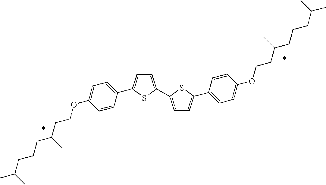 |
S: route B, FIG. 2P: extractionY: 63%, optically pure | |
| 4(2Et)-O-PTTP-O-4(2Et) |  |
S: route B, FIG. 2P: precipitation,extractionY: 37% | solubility in THF about4,900 ppm |
| 6(2Me)-O-PTTP-O-6(2Me) |  |
S: route B, FIG. 2P: extractionY: 47% | sufficiently soluble in THF(about 61,000 ppm)DSC: mp = 197° C. |
| 6(2Et)-O-PTTP-O-6(2Et) | 5,5′-bis(4-(2-ethylhexyloxy)phenyl)-2,2′- |
S: route A, FIG. 2P: chromatographyY: 5%heavy loss during PS: route BP: precipitationY: 29 and 26% | sufficiently soluble in THF(about 70,000 ppm) and o-xylene (about25,000 ppm); viscosity η =22 mPas at c = 500 ppm,cyclohexanol/THFA/THF = 86:9:5)DSC: mp = 148° C., smallertransition between 75° C.and 105° C. (only inheating cycle) |
| 6(1Me)-O-PTTP-O-6(1Me); alsoreferred to as1-MH- |
5,5′bis(4-(1-methylhexyloxy)phenyl)-2,2′-bithiophene |
S: route D, FIG. 2P: filtration (SiO2),Y: 19S: route B, FIG. 2P: extractionY: 52, 37, 51 and 44%S: route B, FIG. 2P: 2 x precipitation.from toluene with methanolY: 39% | well soluble in THF (about89,000 ppm); o-xylene54,000 ppm;THF/cyclohexanol 2:8( |
| 6(1Et)-O-PTTP-O-6(1Et) |  |
S: route B, FIG. 2P: extractionY: 55% | Well soluble in THF(about 330,000 ppm)DSC: mp = 97-102° C.,(broad transition) |
| 6(6TBDPSO)-O-PTTP-O-6(6TBDPSO) |  |
S: route B, FIG. 2P: extractionY: 74%Precursor for terminalOH-alkyl PTTP | Well soluble in THF(about 310,000 ppm); |
| 3(3THPO,2Me)-O-PTTP-O-3(THPO,2Me) |  |
S: route B, FIG. 2P: extractionY: 48% | Well soluble in THF(about 75,000 ppm) |
| 3(3OH,2Me)-O-PTTP-O-3(3OH,2Me) |  |
S: route B, FIG. 2P: extractionY: 59% | Low solubility in THF(600 ppm) |
| 5[5(1,4diene)O2C]-O-PTTP-O-5[5(1,4dieneO2C] |  |
S: route B, FIG. 2P: precipitationY: 64% | well soluble in THF(131,000 ppm) |
| 3O2PTTP2O3 |  |
S: route F, reportedbelow. | Solubility like6PTTP6 |

p-Bromophenol (295.52 grams (“g”), 1500.00 millimole) is dissolved in anhydrous dimethyl formamide (“DMF”) (500 milliliters) in a 2000 milliliter (“mL”) 3-necked flask equipped with mechanical stirrer and condenser, under an argon atmosphere. To this solution, (1-methyl) hexylbromide (322.38 grams, 1800.00 millimoles), sodium iodide (33.57 g, 225.00 mmol) and anhydrous potassium carbonate (621.95 g, 4500.00 mmol) are added. The resulting suspension is heated to 100° C. and stirred at that temperature for 72 hours. After cooling to room temperature, water (1000 mL) and n-hexane (300 mL) are added. The aqueous layer is separated and extracted with n-hexane (3×100 mL). The combined organic layers are washed with diluted sodium chloride solution (2×100 mL) and dried (MgSO4). The solvent is removed by rotary evaporation under reduced pressure and the residue is filtered using a SiO2 layer (10×10 cm) and n-hexane as eluent. After removal of solvent by rotary evaporation and in vacuo a colorless liquid (245.54 g, 60%) is obtained.

Tetrakistriphenylphosphinpalladium(0), (20.45 g, 17.70 mmol) is suspended in anhydrous DMF (400 mL) in a 2000 mL 3-necked flask with magnetic stirrer and condenser under an argon atmosphere. To this, 1-bromo-4-(1-methyl-hexyloxy)-benzene (240.00 g, 884.96 mmol) and tri-n-butylstannylthiophene (330.24 g, 884.96 mmol) are added. The resulting solution is stirred at 100° C. for 68 hours. After cooling to room temperature the mixture is poured into water (2000 mL) and divided into two portions of the same volume. Extraction with n-hexane (3×300 mL) results in two layers and an emulsion between those two layers. The organic layers are separated, combined, washed with diluted sodium chloride solution (2×400 mL) and dried (MgSO4). After removal of solvent by rotary evaporation most of the byproducts are removed by distillation (p=10−3 millibar, maximum temperature Tmax=130° C.). The residue is subjected to filtration using a layer of SiO2 (30×10 cm) and n-hexane as eluent. After removal of solvent, a yellowish oil (107.88 g, about 44%) with sufficient purity for synthetic purposes is obtained.

In a 2000 mL 3-necked flask equipped with mechanical stirrer, condenser and dropping funnel, 2-[4-(1-Methyl-hexyloxy)-phenyl]-thiophene (26.00 g, 94.74 mmol) is dissolved in anhydrous tetrahydrofuran (“THF”) (250 mL) under an argon atmosphere. Then n-BuLi (2.5M in hexanes, 41.68 mL, 104.22 mmol) is added at −70° C. within about 15 min by a syringe. The solution is stirred for 1 h at that temperature. A solution of tris-(2,4-pentadionato)-iron(III) (33.48 g, 94.74 mmol) in anhydrous THF (400 mL) is transferred to the dropping funnel under an argon atmosphere and added to the lithiated 2-[4-(1-Methyl-hexyloxy)-phenyl]-thiophene at −70° C. within about 45 min. The mixture is then allowed to warm to room temperature and heated to reflux for 1 h. After cooling the solvents are removed by rotary evaporation under reduced pressure. The residue is transferred to an extraction thimble and extracted with MeOH (900 mL) overnight using a Soxhlet-apparatus to remove most of the iron compounds. The deep orange colored extract is discarded and the thimble is dried in a continuous stream of nitrogen. The extraction is continued to completeness using n-hexane (900 mL). From the extract the product precipitates upon cooling as a pale orange solid. After separation of the solid by filtration using a folded filter and drying, it is extracted a second time using methanol (900 mL) for about 2 h until the extract is pale yellow. The methanolic solution is discarded and the thimble is dried as described above. Complete extraction using n-hexane (900 mL) and cooling of the resulting solution yields the pure product as a bright yellow solid (10.78 g, 42%).


This fluorinated low k dielectric material is commercially available from Sigma-Aldrich under the trade name Teflon® AF 2400 (catalogue number 469629).
| TABLE 2 | ||
| Dielectric composition | Dielectric constant | volume resistivity (Ωcm) |
| PVA | 7.8*** | 8 × 1012* 8 × 1013** |
| PVP | 2.4**** | 3 × 1013* 4 × 1011** |
| PVP/BaTiO3 dispersion | 26.5**** | 1 × 1011* 1 × 1013** |
| Cytop ® Perfluoro(1- | 2.1*** | 3 × 1015* 6 × 1014** |
| butenyl vinyl ether) | ||
| | ||
| PU | ||
| 6*** | 1 × 10¹³-1 × 10¹⁴*** | |
| |
40*** | |
| *after 10 minutes drying at 80° C. | ||
| **after 10 minutes drying at 80° C. and then 5 minutes at room temperature in air | ||
| ***at room temperature in air | ||
| ****at 25° C., 50% relative humidity | ||
| TABLE 2 | |||
| 6(1Me)-O-PTTP-O-6(1Me) | 5,5′-bis(4-(1-methylhexyloxy)phenyl)-2,2′-bithiophene |
S: route D, FIG. 2P: filtration (SiO2),extractionY: 19S: route B, FIG. 2P: extractionY: 52, 36, 51, and 44%S: route B, FIG. 2P: 2 x precipitation fromtoluene with methanolY: 39% | well soluble in THF (about89,000); o-xylene54,000 ppm;THF/cyclohexanol 2:8( |
| 7(2Me)-PTTP-7(2Me) |  |
S: FIG. 3P: extractionY: 54% | well soluble in THF, butnot better than oxygen-containing analogue“6(1Me)-O” (about45,000 ppm) |
I ds =W/2L×C iμ(Vg−Vt)2 (2)
In formula (2), Ids is the saturation drain-source current, W is the width of the source-drain gap, L is the length of the gap, Ci is the capacitance of the organic dielectric composition body, μ is the mobility in cm2/Vs, Vg is the gate electrode voltage and Vt is the threshold voltage. An applied drain-source current within a range of between −100 volts and 0 volts at intervals of −20 volts was used in testing the transistors. The capacitance of the organic dielectric composition bodies in the FETs was directly measured by probes attached to a Hewlett-Packard inductance-capacitance-resistance meter with an applied current. The W/L ratio was measured by using an optical microscope.
μ=(∂I ds /∂Vg)·(L/WciV ds) (3)
In formula (3), Ids is the drain-source (or source-drain) current in the linear regime (IVdI <IVgI). Vg is the gate electrode voltage, Vds is the drain-source (or source-drain) voltage, Ci is the gate insulator capacitance per unit area, L is the channel length, W is the channel width, and ∂ denotes a partial derivative. The voltages for the measurement of the output characteristics were varied in the following range: 0V≧Vds≧−60 V (10 V steps), 10 V≧Vgs≧−60 V (10 V steps). The gate insulator capacitance in the FETs was directly measured by probes attached to the Hewlett-Packard inductance-capacitance-resistance meter. The W/L ratio was measured using an optical microscope.
Claims (19)


Priority Applications (4)
| Application Number | Priority Date | Filing Date | Title |
|---|---|---|---|
| US11/241,642 US7488834B2 (en) | 2005-09-30 | 2005-09-30 | Organic semiconductors |
| AT06793928T ATE532779T1 (en) | 2005-09-30 | 2006-09-29 | PHENYLENE-THIOPHENE OLIGOMERS AS ORGANIC SEMICONDUCTORS |
| EP06793928A EP1943239B1 (en) | 2005-09-30 | 2006-09-29 | Phenylene-thiophene oligomers as organic semiconductors |
| PCT/EP2006/066914 WO2007039574A1 (en) | 2005-09-30 | 2006-09-29 | Phenylene-thiophene oligomers as organic semiconductors |
Applications Claiming Priority (1)
| Application Number | Priority Date | Filing Date | Title |
|---|---|---|---|
| US11/241,642 US7488834B2 (en) | 2005-09-30 | 2005-09-30 | Organic semiconductors |
Publications (2)
| Publication Number | Publication Date |
|---|---|
| US20070078267A1 US20070078267A1 (en) | 2007-04-05 |
| US7488834B2 true US7488834B2 (en) | 2009-02-10 |
Family
ID=37420940
Family Applications (1)
| Application Number | Title | Priority Date | Filing Date |
|---|---|---|---|
| US11/241,642 Expired - Fee Related US7488834B2 (en) | 2005-09-30 | 2005-09-30 | Organic semiconductors |
Country Status (4)
| Country | Link |
|---|---|
| US (1) | US7488834B2 (en) |
| EP (1) | EP1943239B1 (en) |
| AT (1) | ATE532779T1 (en) |
| WO (1) | WO2007039574A1 (en) |
Families Citing this family (7)
| Publication number | Priority date | Publication date | Assignee | Title |
|---|---|---|---|---|
| US8003435B2 (en) * | 2004-12-17 | 2011-08-23 | Konica Minolta Holdings, Inc. | Method of manufacturing organic film transistor |
| US20070075630A1 (en) * | 2005-09-30 | 2007-04-05 | Florian Dotz | Organic compositions |
| US8190699B2 (en) * | 2008-07-28 | 2012-05-29 | Crossfield Technology LLC | System and method of multi-path data communications |
| WO2011020712A2 (en) | 2009-08-18 | 2011-02-24 | Universite Libre De Bruxelles | Oligothiophenes derivatives |
| US8890234B2 (en) * | 2012-09-05 | 2014-11-18 | Kabushiki Kaisha Toshiba | Nonvolatile semiconductor memory device |
| WO2018095392A1 (en) * | 2016-11-23 | 2018-05-31 | 广州华睿光电材料有限公司 | Organic mixture, composition, and organic electronic component |
| CN110201613B (en) * | 2019-06-10 | 2021-09-14 | 东莞东阳光科研发有限公司 | Polystyrene magnetic microsphere and preparation method thereof |
Citations (15)
| Publication number | Priority date | Publication date | Assignee | Title |
|---|---|---|---|---|
| US6265243B1 (en) | 1999-03-29 | 2001-07-24 | Lucent Technologies Inc. | Process for fabricating organic circuits |
| WO2002045184A1 (en) | 2000-11-28 | 2002-06-06 | Avecia Limited | Field effect transistors and materials and methods for their manufacture |
| US6403397B1 (en) | 2000-06-28 | 2002-06-11 | Agere Systems Guardian Corp. | Process for fabricating organic semiconductor device involving selective patterning |
| WO2003052841A1 (en) | 2001-12-19 | 2003-06-26 | Avecia Limited | Organic field effect transistor with an organic dielectric |
| US20030227014A1 (en) | 2002-06-11 | 2003-12-11 | Xerox Corporation. | Process for forming semiconductor layer of micro-and nano-electronic devices |
| WO2004057688A1 (en) | 2002-12-20 | 2004-07-08 | Avecia Limited | Improvements in and relating to organic semiconducting materials |
| US6803262B2 (en) | 2002-10-17 | 2004-10-12 | Xerox Corporation | Process using self-organizable polymer |
| US6855951B2 (en) | 2003-03-19 | 2005-02-15 | Xerox Corporation | Fluorinated polythiophenes and devices thereof |
| US20050040394A1 (en) | 2003-08-22 | 2005-02-24 | Xerox Corporation. | Semiconductor polymers and devices thereof |
| DE10340643A1 (en) | 2003-09-03 | 2005-04-07 | Siemens Ag | Polymer blends for printed polymer electronics circuits |
| US6890868B2 (en) | 2002-10-17 | 2005-05-10 | Xerox Corporation | Process for depositing gelable composition that includes dissolving gelable composition in liquid with agitating to disrupt gelling |
| US6897284B2 (en) | 2003-03-19 | 2005-05-24 | Xerox Corporation | Polythiophenes and devices thereof |
| US20050184274A1 (en) | 2004-02-25 | 2005-08-25 | Martin Heeney | Reactive mesogenic charge transport compounds |
| US20050205861A1 (en) | 2004-03-17 | 2005-09-22 | Lucent Technologies Inc. | P-type OFET with fluorinated channels |
| WO2006024012A1 (en) | 2004-08-23 | 2006-03-02 | E.I. Dupont De Nemours And Company | P-alkoxyphenylen-thiophene oligomers as organic semiconductors for use in electronic devices |
-
2005
- 2005-09-30 US US11/241,642 patent/US7488834B2/en not_active Expired - Fee Related
-
2006
- 2006-09-29 AT AT06793928T patent/ATE532779T1/en active
- 2006-09-29 WO PCT/EP2006/066914 patent/WO2007039574A1/en active Application Filing
- 2006-09-29 EP EP06793928A patent/EP1943239B1/en not_active Not-in-force
Patent Citations (16)
| Publication number | Priority date | Publication date | Assignee | Title |
|---|---|---|---|---|
| US6551717B2 (en) | 1999-03-29 | 2003-04-22 | Lucent Technologies Inc. | Process for fabricating organic circuits |
| US6265243B1 (en) | 1999-03-29 | 2001-07-24 | Lucent Technologies Inc. | Process for fabricating organic circuits |
| US6403397B1 (en) | 2000-06-28 | 2002-06-11 | Agere Systems Guardian Corp. | Process for fabricating organic semiconductor device involving selective patterning |
| WO2002045184A1 (en) | 2000-11-28 | 2002-06-06 | Avecia Limited | Field effect transistors and materials and methods for their manufacture |
| WO2003052841A1 (en) | 2001-12-19 | 2003-06-26 | Avecia Limited | Organic field effect transistor with an organic dielectric |
| US20030227014A1 (en) | 2002-06-11 | 2003-12-11 | Xerox Corporation. | Process for forming semiconductor layer of micro-and nano-electronic devices |
| US6890868B2 (en) | 2002-10-17 | 2005-05-10 | Xerox Corporation | Process for depositing gelable composition that includes dissolving gelable composition in liquid with agitating to disrupt gelling |
| US6803262B2 (en) | 2002-10-17 | 2004-10-12 | Xerox Corporation | Process using self-organizable polymer |
| WO2004057688A1 (en) | 2002-12-20 | 2004-07-08 | Avecia Limited | Improvements in and relating to organic semiconducting materials |
| US6855951B2 (en) | 2003-03-19 | 2005-02-15 | Xerox Corporation | Fluorinated polythiophenes and devices thereof |
| US6897284B2 (en) | 2003-03-19 | 2005-05-24 | Xerox Corporation | Polythiophenes and devices thereof |
| US20050040394A1 (en) | 2003-08-22 | 2005-02-24 | Xerox Corporation. | Semiconductor polymers and devices thereof |
| DE10340643A1 (en) | 2003-09-03 | 2005-04-07 | Siemens Ag | Polymer blends for printed polymer electronics circuits |
| US20050184274A1 (en) | 2004-02-25 | 2005-08-25 | Martin Heeney | Reactive mesogenic charge transport compounds |
| US20050205861A1 (en) | 2004-03-17 | 2005-09-22 | Lucent Technologies Inc. | P-type OFET with fluorinated channels |
| WO2006024012A1 (en) | 2004-08-23 | 2006-03-02 | E.I. Dupont De Nemours And Company | P-alkoxyphenylen-thiophene oligomers as organic semiconductors for use in electronic devices |
Non-Patent Citations (24)
Also Published As
| Publication number | Publication date |
|---|---|
| EP1943239B1 (en) | 2011-11-09 |
| EP1943239A1 (en) | 2008-07-16 |
| ATE532779T1 (en) | 2011-11-15 |
| US20070078267A1 (en) | 2007-04-05 |
| WO2007039574A1 (en) | 2007-04-12 |
Similar Documents
| Publication | Publication Date | Title |
|---|---|---|
| US7488834B2 (en) | Organic semiconductors | |
| US7800103B2 (en) | Organic thin film transistor material, organic thin film transistor, field-effect transistor, switching element, organic semiconductor material and organic semiconductor film | |
| US7795611B2 (en) | Field effect organic transistor | |
| US9133211B2 (en) | Dithienobenzodithiophene semiconductive material and electronic device using the same | |
| CA2613719C (en) | Thiophene electronic devices | |
| JP5307349B2 (en) | Functionalized heteroacenes and electronic devices made therefrom | |
| US20060202191A1 (en) | Semiconductors containing perfluoroether acyl oligothiohpene compounds | |
| US7569415B2 (en) | Liquid phase fabrication of active devices including organic semiconductors | |
| EP3141551A1 (en) | Organic semiconductors | |
| US9564604B2 (en) | Fused polycyclic aromatic compounds, organic semiconductor material and thin film including the same, and method for producing an organic semiconductor device | |
| US20060220007A1 (en) | Acene compounds having a single terminal fused thiophene as semiconductor materials for thin film transistors and methods of making the same | |
| US7732812B2 (en) | Active semiconductor devices | |
| EP2213692A1 (en) | Polymer Semiconductors with High Mobility | |
| US20070075630A1 (en) | Organic compositions | |
| US7928181B2 (en) | Semiconducting polymers | |
| US7872258B2 (en) | Organic thin-film transistors | |
| US8946448B2 (en) | Organic semiconductors | |
| US20110215306A1 (en) | Organic semiconductor element and organic electrode | |
| US7928433B2 (en) | Electronic device comprising semiconducting polymers | |
| WO2011052285A1 (en) | Novel compound, field-effective transistor, solar cell, method for producing said compound, field-effective transistor, and solar cell, composition for organic semiconductor layer, and composition for p-type semiconductor layer | |
| JP5218812B2 (en) | Organic thin film transistor | |
| US8420440B2 (en) | Semiconducting composition | |
| US8283659B2 (en) | Tetrahydrotetraazapentacenes in thin-film transistors | |
| JP2004165428A (en) | Organic thin film transistor element |
Legal Events
| Date | Code | Title | Description |
|---|---|---|---|
| AS | Assignment |
Owner name: LUCENT TECHNOLOGIES INC., NEW JERSEY Free format text: ASSIGNMENT OF ASSIGNORS INTEREST;ASSIGNORS:KATZ, HOWARD E.;REICHMANIS, ELSA;VAIDYANATHAN, SUBRAMANIAN;REEL/FRAME:017306/0397;SIGNING DATES FROM 20060103 TO 20060127 |
|
| FEPP | Fee payment procedure |
Free format text: PAYOR NUMBER ASSIGNED (ORIGINAL EVENT CODE: ASPN); ENTITY STATUS OF PATENT OWNER: LARGE ENTITY |
|
| AS | Assignment |
Owner name: ALCATEL-LUCENT USA INC., NEW JERSEY Free format text: MERGER;ASSIGNOR:LUCENT TECHNOLOGIES INC.;REEL/FRAME:022000/0218 Effective date: 20081101 |
|
| AS | Assignment |
Owner name: BASF SOCIETAS EUROPAEA, GERMANY Free format text: ASSIGNMENT OF ASSIGNORS INTEREST;ASSIGNORS:DOTZ, FLORIAN;HENNIG, INGOLF;REEL/FRAME:022014/0725;SIGNING DATES FROM 20080428 TO 20080509 |
|
| FPAY | Fee payment |
Year of fee payment: 4 |
|
| AS | Assignment |
Owner name: CREDIT SUISSE AG, NEW YORK Free format text: SECURITY INTEREST;ASSIGNOR:ALCATEL-LUCENT USA INC.;REEL/FRAME:030510/0627 Effective date: 20130130 |
|
| AS | Assignment |
Owner name: ALCATEL-LUCENT USA INC., NEW JERSEY Free format text: RELEASE BY SECURED PARTY;ASSIGNOR:CREDIT SUISSE AG;REEL/FRAME:033950/0001 Effective date: 20140819 |
|
| REMI | Maintenance fee reminder mailed | ||
| LAPS | Lapse for failure to pay maintenance fees | ||
| STCH | Information on status: patent discontinuation |
Free format text: PATENT EXPIRED DUE TO NONPAYMENT OF MAINTENANCE FEES UNDER 37 CFR 1.362 |
|
| FP | Lapsed due to failure to pay maintenance fee |
Effective date: 20170210 |