US6803262B2 - Process using self-organizable polymer - Google Patents
Process using self-organizable polymer Download PDFInfo
- Publication number
- US6803262B2 US6803262B2 US10/273,901 US27390102A US6803262B2 US 6803262 B2 US6803262 B2 US 6803262B2 US 27390102 A US27390102 A US 27390102A US 6803262 B2 US6803262 B2 US 6803262B2
- Authority
- US
- United States
- Prior art keywords
- polymer
- liquid
- layer
- structurally ordered
- solubility
- Prior art date
- Legal status (The legal status is an assumption and is not a legal conclusion. Google has not performed a legal analysis and makes no representation as to the accuracy of the status listed.)
- Expired - Lifetime, expires
Links
Images


Classifications
-
- H—ELECTRICITY
- H10—SEMICONDUCTOR DEVICES; ELECTRIC SOLID-STATE DEVICES NOT OTHERWISE PROVIDED FOR
- H10K—ORGANIC ELECTRIC SOLID-STATE DEVICES
- H10K71/00—Manufacture or treatment specially adapted for the organic devices covered by this subclass
- H10K71/10—Deposition of organic active material
- H10K71/191—Deposition of organic active material characterised by provisions for the orientation or alignment of the layer to be deposited
-
- H—ELECTRICITY
- H10—SEMICONDUCTOR DEVICES; ELECTRIC SOLID-STATE DEVICES NOT OTHERWISE PROVIDED FOR
- H10K—ORGANIC ELECTRIC SOLID-STATE DEVICES
- H10K85/00—Organic materials used in the body or electrodes of devices covered by this subclass
- H10K85/10—Organic polymers or oligomers
- H10K85/111—Organic polymers or oligomers comprising aromatic, heteroaromatic, or aryl chains, e.g. polyaniline, polyphenylene or polyphenylene vinylene
- H10K85/113—Heteroaromatic compounds comprising sulfur or selene, e.g. polythiophene
-
- H—ELECTRICITY
- H10—SEMICONDUCTOR DEVICES; ELECTRIC SOLID-STATE DEVICES NOT OTHERWISE PROVIDED FOR
- H10K—ORGANIC ELECTRIC SOLID-STATE DEVICES
- H10K85/00—Organic materials used in the body or electrodes of devices covered by this subclass
- H10K85/10—Organic polymers or oligomers
- H10K85/154—Ladder-type polymers
-
- H—ELECTRICITY
- H10—SEMICONDUCTOR DEVICES; ELECTRIC SOLID-STATE DEVICES NOT OTHERWISE PROVIDED FOR
- H10K—ORGANIC ELECTRIC SOLID-STATE DEVICES
- H10K10/00—Organic devices specially adapted for rectifying, amplifying, oscillating or switching; Organic capacitors or resistors having potential barriers
- H10K10/40—Organic transistors
- H10K10/46—Field-effect transistors, e.g. organic thin-film transistors [OTFT]
- H10K10/462—Insulated gate field-effect transistors [IGFETs]
- H10K10/464—Lateral top-gate IGFETs comprising only a single gate
-
- H—ELECTRICITY
- H10—SEMICONDUCTOR DEVICES; ELECTRIC SOLID-STATE DEVICES NOT OTHERWISE PROVIDED FOR
- H10K—ORGANIC ELECTRIC SOLID-STATE DEVICES
- H10K10/00—Organic devices specially adapted for rectifying, amplifying, oscillating or switching; Organic capacitors or resistors having potential barriers
- H10K10/40—Organic transistors
- H10K10/46—Field-effect transistors, e.g. organic thin-film transistors [OTFT]
- H10K10/462—Insulated gate field-effect transistors [IGFETs]
- H10K10/466—Lateral bottom-gate IGFETs comprising only a single gate
-
- H—ELECTRICITY
- H10—SEMICONDUCTOR DEVICES; ELECTRIC SOLID-STATE DEVICES NOT OTHERWISE PROVIDED FOR
- H10K—ORGANIC ELECTRIC SOLID-STATE DEVICES
- H10K85/00—Organic materials used in the body or electrodes of devices covered by this subclass
- H10K85/10—Organic polymers or oligomers
- H10K85/111—Organic polymers or oligomers comprising aromatic, heteroaromatic, or aryl chains, e.g. polyaniline, polyphenylene or polyphenylene vinylene
- H10K85/114—Poly-phenylenevinylene; Derivatives thereof
-
- H—ELECTRICITY
- H10—SEMICONDUCTOR DEVICES; ELECTRIC SOLID-STATE DEVICES NOT OTHERWISE PROVIDED FOR
- H10K—ORGANIC ELECTRIC SOLID-STATE DEVICES
- H10K85/00—Organic materials used in the body or electrodes of devices covered by this subclass
- H10K85/10—Organic polymers or oligomers
- H10K85/111—Organic polymers or oligomers comprising aromatic, heteroaromatic, or aryl chains, e.g. polyaniline, polyphenylene or polyphenylene vinylene
- H10K85/115—Polyfluorene; Derivatives thereof
-
- H—ELECTRICITY
- H10—SEMICONDUCTOR DEVICES; ELECTRIC SOLID-STATE DEVICES NOT OTHERWISE PROVIDED FOR
- H10K—ORGANIC ELECTRIC SOLID-STATE DEVICES
- H10K85/00—Organic materials used in the body or electrodes of devices covered by this subclass
- H10K85/10—Organic polymers or oligomers
- H10K85/151—Copolymers
Definitions
- Polymer thin film transistors have potential applications as key elements of integrated circuits for optoelectronic devices based on solution processing to lower manufacturing cost.
- Polymer thin film transistors generally have lower electrical performance such as lower mobility than do their silicon counterparts such as crystalline silicon or polysilicon thin film transistors. Nevertheless, the electrical performance levels of polymer thin film transistors may be sufficient for many applications, particularly large-area devices such as active matrix liquid crystal display, electronic paper, and certain low-end microelectronics such as smart cards, radio frequency identification tags, and the like, where high switching speeds may not be required. For these applications, low cost is particularly important.
- One main approach to obtaining higher charge carrier mobility for polymer thin film transistors is to achieve higher degrees of structural order in the active semiconducting polymer layer.
- PCT WO 00/79617 A1 discloses the alignment of the polymer chains parallel to each other by bringing the polymer into a liquid-crystalline phase. There is a need, which the present invention addresses, for new techniques applicable to the fabrication of electronic devices to induce increased structural order in semiconducting polymers.
- composition comprising a liquid and a self-organizable polymer at least partially dissolved in the liquid, resulting in dissolved polymer molecules;
- composition comprising a liquid and a self-organizable polymer at least partially dissolved in the liquid, resulting in dissolved polymer molecules, wherein the polymer is polythiophene;
- the reducing the solubility of the dissolved polymer molecules to induce formation of structurally ordered polymer aggregates in the composition, wherein the reducing the solubility of the dissolved polymer molecules is accomplished by adding a different liquid that is less capable of dissolving the polymer than the liquid;
- the insulating layer, the gate electrode, the semiconductor layer, the source electrode, and the drain electrode are in any sequence as long as the gate electrode and the semiconductor layer both contact the insulating layer, and the source electrode and the drain electrode both contact the semiconductor layer,
- the semiconductor layer is prepared by a process comprising:
- composition comprising a liquid and a self-organizable polymer at least partially dissolved in the liquid, resulting in dissolved polymer molecules;
- FIG. 1 represents a first embodiment of a thin film transistor made using the present process
- FIG. 2 represents a second embodiment of a thin film transistor made using the present process
- FIG. 3 represents a third embodiment of a thin film transistor made using the present process.
- FIG. 4 represents a fourth embodiment of a thin film transistor made using the present process.
- Any suitable self-organizable polymer which is capable of increased structural order in response to reduced solubility of the polymer in a selected liquid may be used in the present invention.
- Molecular self-organization refers to the ability of molecules to organize themselves into a higher molecular and intermolecular structural order in response to a stimulus such as solvency in a liquid.
- one, two, three, or more self-organizable polymers may be used.
- the self-organizable polymer may or may not precipitate in the liquid.
- the polymer may be considered to exhibit poor solubility in a liquid when the concentration of the polymer in a saturated solution in that liquid is not high enough to make a thin polymer layer that is useful for the intended applications by common deposition techniques. Generally, when the concentration of the polymer in a particular liquid is below about 0.1 percent by weight, its solubility in that liquid is deemed to be poor. Even though the polymer may exhibit low solubility in a liquid at room temperature, its solubility can generally be increased by heating above room temperature.
- the concentration is higher than about 0.2 percent by weight, the polymer is considered to exhibit reasonable solubility as a useful thin polymer layer may be fabricated from this solution using common deposition processes.
- room temperature refers to a temperature ranging from about 22 to about 25 degrees C.
- the self-organizable polymer may be a conjugated polymer such as for instance polythiophenes, polyphenylenes, polyphenylene derivatives, polyfluorenes, fluorene copolymers, and ladder polymers.
- Exemplary polythiophenes include for instance the following:
- n is from about 5 to about 5,000.
- Suitable polythiophenes are disclosed in U.S. Ser. No. 10/042,356, U.S. Ser. No. 10/042,358, and U.S. Ser. No. 10/042,342, the disclosures of which are totally incorporated herein by reference.
- Exemplary polyphenylenes and polyphenylene derivatives include for instance the following:
- R 1 and R 2 may be the same or different from each other and are a side chain comprised of, for example, alkyl derivatives such as alkoxyalkyl and siloxy-subsituted alkyl, perhaloalkyl such as perfluoroalkyl, polyether such as oligoethylene oxide, polysiloxy derivatives, and the like, containing from about 4 to about 50 atoms.
- alkyl derivatives such as alkoxyalkyl and siloxy-subsituted alkyl
- perhaloalkyl such as perfluoroalkyl
- polyether such as oligoethylene oxide, polysiloxy derivatives, and the like, containing from about 4 to about 50 atoms.
- Exemplary polyphenylenes, and polyphenylene derivatives such as poly(phenylene vinylene)s and poly(phenylene ethynylene)s, are disclosed in “The electroluminescence of organic materials” by U. Mitschke and P. Bäuerle
- Exemplary polyfluorenes and fluorene copolymers include for instance the following:
- R 1 and R 2 may be the same or different from each other and are hydrogen or a side chain comprised of, for example, alkyl derivatives such as alkoxyalkyl and siloxy-subsituted alkyl, perhaloalkyl such as perfluoroalkyl, polyether such as oligoethylene oxide, polysiloxy derivatives, and the like, containing from about 4 to 50 atoms.
- alkyl derivatives such as alkoxyalkyl and siloxy-subsituted alkyl
- perhaloalkyl such as perfluoroalkyl
- polyether such as oligoethylene oxide, polysiloxy derivatives, and the like, containing from about 4 to 50 atoms.
- Exemplary polyfluorenes and fluorene copolymers are disclosed in “New Well-Defined Poly(2,7-fluorene) Derivatives: Photoluminescence and Base Doping,” by M. Ranger, D. Rondeau, M. Leclerc
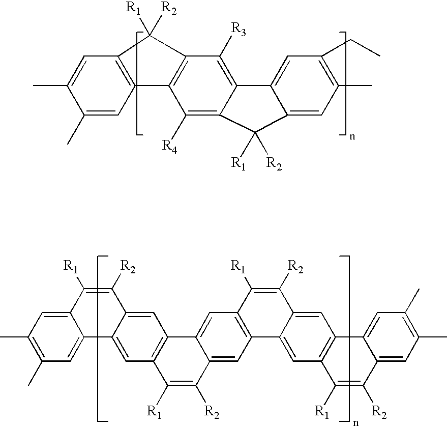
- Exemplary ladder polymers include for instance ladder-type polyphenylene and ladder-type polyacene
- R 1 , R 2 , R 3 , and R 4 may be the same or different from each other and are a side chain comprised of, for example, alkyl derivatives such as alkoxyalkyl and siloxy-subsituted alkyl, perhaloalkyl such as perfluoroalkyl, polyether such as oligoethylene oxide, polysiloxy derivatives, alkyl or alkoxyalkyl-substituted phenylene, and the like, containing from about 4 to 60 atoms.
- Exemplary ladder polymers are disclosed in “Ladder-type materials” by U. Scherf, J. Mater. Chem . (1999), Vol. 9, pp. 1853-1864, the disclosure of which is totally incorporated herein by reference.
- the polymer or polymers are completely dissolved or partially dissolved in a liquid prior to the reducing the solubility of the polymer or polymers in the liquid. Stirring may be optionally employed to aid the dissolution. Undissolved polymer may be optionally removed by filtration.
- the amount of the polymer dissolved in the liquid may range for example from about 0.1% to as much as about 50% by weight of the polymer.
- the concentration of the polymer in the liquid ranges for example from about 0.1% to about 30% by weight, particularly from about 0.2% to about 10% by weight, based on the total weight of the liquid and the polymer.
- the polymer concentrations in the liquid described above are before reducing the solubility of the polymer in the liquid.
- Heat may be optionally employed to aid the dissolution of the polymer at an elevated temperature, for a period of time ranging for instance from about 1 minutes to about 24 hours, particularly from about 10 minutes to about 4 hours.
- the phrase “elevated temperature” refers to a temperature ranging from above room temperature to the boiling point or higher of the chosen liquid (at one atmosphere or higher pressure), for example from about 40 to about 180 degrees C., particularly from about 50 to about 120 degrees C.
- the liquid may be a fair to excellent solvent for the polymer at room temperature or at an elevated temperature.
- the liquid may be for instance chloroform, tetrahydrofuran, chlorobenzene, dichlorobenzene, trichlorobenzene, nitrobenzene, toluene, xylene, mesitylene, 1,2,3,4-tetrahydronaphthelene, dichloromethane, 1,2-dichloroethane trichloroethane, 1,1,2,2,-chloroethane, or a mixture thereof.
- any suitable technique may be used to reduce the solubility of the dissolved polymer molecules in the liquid to induce the formation of structurally ordered polymer aggregates.
- a different liquid may be added that is less or not capable of dissolving the polymer compared to the liquid, i.e., the liquid is a better solvent than the different liquid.
- the different liquid is added in an amount ranging from about 1% to about 80% by volume based on the total volume of the liquid and the different liquid, for a period of time ranging for instance from about 1 minutes to about 4 hours, particularly from about 10 minutes to about 1 hour. Agitation is optionally used during addition of the different liquid.
- the different liquid may be for instance methanol, ethanol, isopropanol, hexane, heptane, acetone, and water. Therefore, the resultant composition is comprised of the polymer or polymers and the combination of the liquid and the different liquid which can be the combination of chlorobenzene/hexane, chlorobenzene/heptane, chloroform/methanol, tetrahydrofuran/methanol, and tetrahydrofuran/water.
- the reducing the solubility of the dissolved polymer molecules is accomplished by changing the temperature of the composition.
- heat may be used to aid dissolution of the polymer in the liquid at a temperature and for a time as discussed herein. Then the temperature is lowered from the elevated temperature to room temperature or by an amount ranging for instance from about 10 to about 150 degrees C., particularly from about 20 to about 100 degrees C., and wherein the lowered temperature is maintained for a period of time ranging for example from about 10 minutes to about 10 hours, particularly from about 30 minutes to about 4 hours.
- Any combination of techniques can be used to reduce the solubility of the dissolved polymer molecules such as using both a different liquid and controlling the temperature as described herein.
- aggregates tend to come together in aggregate forms when their solubility in the liquid is reduced. These aggregates may be amorphous (i.e., disordered) or highly ordered in nature, depending primarily on the polymer structures, the media they are in, and the conditions under which-the-solubility-reduction occurs.
- structurally ordered polymer aggregates refers to the aggregation of polymer molecules wherein the spatial orientations or arrangements of the molecules relative to their surrounding neighboring molecules within the aggregation are orderly in nature. For instance the polymer molecules may align themselves with their backbones parallel to one another.
- Changes in molecular ordering of the polymer in a composition may be monitored by spectroscopic methods, for instance, absorption spectroscopy, optical spectroscopy, NMR, light scattering and X-ray diffractions analysis, and by transmission electron microscopy.
- a known example is regioregular poly(3-alkylthiophene-2,5-diyl)s which forms ⁇ -stacked lamellar structures as a results of its side chain alignment as disclosed in the reference, “Extensive Studies on ⁇ -Stacking of Poly(3-alkylthiophene-2,5-diyl)s and Poly(4-alkylthiazole-2,5-diyl)s by Optical Spectroscopy, NMR Analysis, Light Scattering Analysis and X-ray Crystallography” by T. Yamamoto, et al., J. Am. Chem. Soc . (1998), Vol 120, pp. 2047-2058.
- the existence of the structural order (of the polymer aggregates) is supported by for example spectroscopy where in an absorption spectrum the absorption maxima shifts toward longer wavelengths together with the appearance of absorption fine structures (e.g., vibronic splitting).
- Reducing the solubility of the dissolved polymer molecules is accomplished with or without visually observable precipitation of the polymer. In embodiments, reducing the solubility of the dissolved polymer molecules is accomplished prior to the point that precipitation starts. In other embodiments, reducing the solubility of the dissolved polymer molecules is accomplished beyond the point that precipitation starts. How much of the different liquid to add or how much should the temperature drop be to reduce the solubility of the dissolved polymer molecules may be determined for example on a trial and error basis. Precipitated polymer may be optionally filtrated out prior to deposition of the layer of the composition containing the structurally ordered polymer aggregates.
- solution coating refers to any liquid composition compatible coating technique such as spin coating, blade coating, rod coating, screen printing, ink jet printing, stamping and the like.
- the composition may be at any suitable temperature.
- the deposition is accomplished at a “lower temperature” below the elevated temperature.
- the “lower temperature” may be a temperature ranging from below room temperature to below the elevated temperature such as for example from about 10 to about 80 degrees C., particularly from about 20 to about 40 degrees C., and especially at room temperature. Where the lower temperature is below room temperature, suitable cooling apparatus may be employed to accomplish this.
- the deposited layer is at least partially dried, especially completely dried, using any suitable technique to remove the liquid (and if used the different liquid).
- the polymer aggregates collapse together and coalesce, resulting in the formation of a continuous film.
- This continuous film contains structurally ordered polymer and thus corresponds to a structurally ordered layer.
- Drying techniques may involve for instance: directing one or more streams of air (at room temperature or at an elevated temperature) at the layer; “natural” evaporation from the layer (i.e., evaporation at room temperature without using an air stream), heating the layer while optionally applying a vacuum, or a combination of drying techniques.
- the elevated temperature may range for instance from about 40 to about 120 degrees C.
- the structurally ordered layer is the semiconductor layer of an electronic device such as a thin film transistor.
- the present process may be used whenever there is a need to form a semiconductor layer in an electronic device.
- electronic device refers to micro- and nano-electronic devices such as, for example, micro- and nano-sized transistors and diodes.
- Illustrative transistors include for instance thin film transistors, particularly organic field effect transistors.
- FIG. 1 there is schematically illustrated a thin film transistor (“TFT”) configuration 10 comprised of a substrate 16 , in contact therewith a metal contact 18 (gate electrode) and a layer of an insulating layer 14 on top of which two metal contacts, source electrode 20 and drain electrode 22 , are deposited. Over and between the metal contacts 20 and 22 is an organic semiconductor layer 12 as illustrated herein.
- TFT thin film transistor
- FIG. 2 schematically illustrates another TFT configuration 30 comprised of a substrate 36 , a gate electrode 38 , a source electrode 40 and a drain electrode 42 , an insulating layer 34 , and an organic semiconductor layer 32 .
- FIG. 3 schematically illustrates a further TFT configuration 50 comprised of a heavily n-doped silicon wafer 56 which acts as both a substrate and a gate electrode, a thermally grown silicon oxide insulating layer 54 , and an organic semiconductor layer 52 , on top of which are deposited a source electrode 60 and a drain electrode 62 .
- FIG. 4 schematically illustrates an additional TFT configuration 70 comprised of substrate 76 , a gate electrode 78 , a source electrode 80 , a drain electrode 82 , an organic semiconductor layer 72 , and an insulating layer 74 .
- composition and formation of the semiconductor layer are described herein.
- the substrate may be composed of for instance silicon, glass plate, plastic film or sheet.
- plastic substrate such as for example polyester, polycarbonate, polyimide sheets and the like may be preferred.
- the thickness of the substrate may be from amount 10 micrometers to over 10 millimeters with an exemplary thickness being from about 50 to about 100 micrometers, especially for a flexible plastic substrate and from about 1 to about 10 millimeters for a rigid substrate such as glass or silicon.
- the gate electrode can be a thin metal film, a conducting polymer film, a conducting film made from conducting ink or paste or the substrate itself, for example heavily doped silicon.
- Examples of gate electrode materials include but are not restricted to aluminum, gold, chromium, indium tin oxide, conducting polymers such as polystyrene sulfonate-doped poly(3,4-ethylenedioxythiophene) (PSS-PEDOT), conducting ink/paste comprised of carbon black/graphite or colloidal silver dispersion in polymer binders, such as Electrodag available from Acheson Colloids Company.
- the gate electrode layer can be prepared by vacuum evaporation, sputtering of metals or conductive metal oxides, coating from conducting polymer solutions or conducting inks by spin coating, casting or printing.
- the thickness of the gate electrode layer ranges for example from about 10 to about 200 nanometers for metal films and in the range of about 1 to about 10 micrometers for polymer conductors.
- the source and drain electrode layers can be fabricated from materials which provide a low resistance ohmic contact to the semiconductor layer. Typical materials suitable for use as source and drain electrodes include those of the gate electrode materials such as gold, nickel, aluminum, platinum, conducting polymers and conducting inks. Typical thicknesses of source and drain electrodes are about, for example, from about 40 nanometers to about 1 micrometer with the more specific thickness being about 100 to about 400 nanometers.
- the insulating layer generally can be an inorganic material film or an organic polymer film.
- inorganic materials suitable as the insulating layer include silicon oxide, silicon nitride, aluminum oxide, barium titanate, barium zirconium titanate and the like;
- organic polymers for the insulating layer include polyesters, polycarbonates, poly(vinyl phenol), polyimides, polystyrene, poly(methacrylate)s, poly(acrylate)s, epoxy resin and the like.
- the thickness of the insulating layer is, for example from about 10 nanometers to about 500 nanometers depending on the dielectric constant of the dielectric material used.
- An exemplary thickness of the insulating layer is from about 100 nanometers to about 500 nanometers.
- the insulating layer may have a conductivity that is for example less than about 10 ⁇ 12 S/cm.
- the insulating layer, the gate electrode, the semiconductor layer, the source electrode, and the drain electrode are formed in any sequence as long as the gate electrode and the semiconductor layer both contact the insulating layer, and the source electrode and the drain electrode both contact the semiconductor layer.
- the phrase “in any sequence” includes sequential and simultaneous formation.
- the source electrode and the drain electrode can be formed simultaneously or sequentially.
- the TFT devices contain a semiconductor channel with a width W and length L.
- the semiconductor channel width may be, for example, from about 1 micrometers to about 5 millimeters, with a specific channel width being about 5 micrometers to about 1 millimeter.
- the semiconductor channel length may be, for example, from about 1 micrometer to about 1 millimeter with a more specific channel length being from about 5 micrometers to about 100 micrometers.
- the source electrode is grounded and a bias voltage of generally, for example, about 0 volt to about ⁇ 80 volts is applied to the drain electrode to collect the charge carriers transported across the semiconductor channel when a voltage of generally about +20 volts to about ⁇ 80 volts is applied to the gate electrode.
- a semiconductor layer comprising the structurally ordered polymer has a carrier mobility greater than for example about 10 ⁇ 3 cm 2 /Vs (centimeters 2 /Volt-second) and a conductivity less than for example about 10 ⁇ 5 S/cm (Siemens/centimeter).
- the thin film transistors produced by the present process have an on/off ratio greater than for example about 10 3 at 20 degrees C.
- the phrase on/off ratio refers to the ratio of the source-drain current when the transistor is on to the source-drain current when the transistor is off.
- the charge transport capability (that is, for drain current and/or carrier mobility) of an inventive electronic device may exceed the charge transport capability of a comparative electronic device that is prepared without inducing the increased structural order in the polymer by an amount ranging for example from about a factor of 1.5 to as much as more than an order of magnitude for each of the drain current and/or charge carrier mobility
- a polythiophene, poly[2,5-bis(2-thienyl)-3,4-dioctylthiophene] (having the structural formula (2) provided earlier in the list of exemplary polythiophenes), was synthesized using the following procedure.
- 3,4-Dioctylthiophene 2 M octylmagnesium bromide (100 milliliters, 0.2 mol) in anhydrous ethyl ether was added to a well-stirred mixture of dichloro[1,3-bis(diphenylphosphino)-propane]nickel(II) (0.2 gram) and 3,4-dibromothiophene (20.16 grams, 0.0833 mol) in 200 milliliters of anhydrous ethyl ether in a 500 milliliter round bottom flask cooled with an ice bath under an inert atmosphere.
- the nickel complex reacted immediately with the Grignard reagent and the resulting reaction mixture was allowed to warm up to room temperature. An exothermic reaction started within 30 minutes and the ethyl ether began to reflux gently. After stirring for another 2 hours at room temperature, the reaction mixture was refluxed for 6 hours, then cooled in an ice bath, and hydrolyzed with aqueous 2N hydrochloric acid. The organic layer was separated and washed successively with water, brine, and again with water, dried over anhydrous sodium sulfate, and filtered. After evaporation of the solvent, the residue was distilled under reduced pressure through Kugelrohr apparatus to provide 21.3 grams of 3,4-dioctylthiophene as a colorless liquid.
- N-bromosuccinimide (4.6 grams, 25.7 mmol) was added to a well-stirred solution of 3,4-dioctylthiophene (3.6 grams, 11.7 mmol) in a mixture of 30 milliliters of dichloromethane and 10 milliliters of acetic acid in a 100 milliliter round-bottomed flask. The reaction was monitored by thin layer chromatography and was complete in about 35 minutes. The mixture was diluted with 160 milliliters of dichloromethane and filtered to remove succinimide.
- 2,5-Bis(2-thienyl)-3,4-dioctylthiophene In a dry box under an inert atmosphere, Pd(PPh 3 ) 2 Cl 2 (0.15 gram, 0.2 mmol) was added to a mixture of 2,5dibromo-3,4-dioctylthiophene (4.2 grams, 9.0 mmol) and 2-(tributylstannyl)-thiophene (7.4 grams, 19.8 mmol) in anhydrous tetrahydrofuran (50 milliliters) in a 250 milliliter round-bottomed flask. The mixture was then refluxed for 12 hours and the solvent was removed by evaporation. The crude product thus obtained was purified by flash chromatography on silica gel using hexane as eluent to give 3.1 grams of 2,5-bis(2thienyl)-3,4-dioctylthiophene.
- N-bromo succinimide (2.8 grams, 15.7 mmol) was added to a well-stirred solution of 2,5-bis(2-thienyl)-3,4-dioctylthiophene (3.6 grams, 7.6 mmol) of N,N-dimethylformamide (30 milliliters) in a 100 milliliter round-bottomed flask cooled with an ice-bath. After addition, the mixture was allowed to warm up to room temperature slowly. The reaction was monitored by thin layer chromatography and was stopped after 3 hours of reaction.
- the polymer was first dissolved in chlorobenzene which was a good solvent at 2 weight percent level. The solution was filtered through a 0.2 ⁇ m syringe filter. A poor solvent such as hexane was then added slowly under shaking or stirring in an amount of about 50% by volume. No precipitation of the polymer was observed. The mixture (polymer, chlorobenzene, and hexane) was very stable. It can be stored at room temperature for weeks without precipitation. This mixture is ready for device fabrication.
- a bottom-contact thin film transistor structure as schematically described by FIG. 1, was chosen as the primary test device configuration in this example.
- the bottom-contact test device was comprised of a series of photolithographically pre-patterned transistor dielectric layers and electrodes with defined channel widths and lengths on a glass substrate.
- the gate electrode on the glass substrate was comprised of chromium of about 80 nanometers in thickness.
- the insulating layer was a 300 nanometers thick silicon nitride having a capacitance of about 22 nF/cm 2 (nanofarads/square centimeter).
- the source and drain contacts comprised of gold of about 100 nanometers in thickness.
- the polythiophene semiconductor layer of about 30 nanometers to 100 nanometers in thickness was then deposited by spin coating from the composition (polymer, chlorobenzene, and hexane). The spin coating was accomplished at a spinning speed of 1,000 rpm for about 35 seconds. The resulting coated device was dried in vacuo at 80° C. for 20 hours, and was then ready for evaluation.
- I SD C i ⁇ ( W /2 L )( V G ⁇ V T ) 2 (1)
- I SD is the drain current at the saturated regime
- W and L are, respectively, the semiconductor channel width and length
- C i is the capacitance per unit area of the insulating layer
- V G and V T are, respectively, the gate voltage and threshold voltage.
- An important property for the thin film transistor is its current on/off ratio, which is the ratio of the saturation source-drain current when the gate voltage V G is equal to or greater than the drain voltage V D to the source-drain current when the gate voltage V G is zero.
- At least five thin film transistors were prepared using the same procedures of Example 1 except that the polythiophene semiconductor layer was deposited from pure good solvent, chlorobenzene (that is, no hexane was added).
- Example 1 A dramatic performance enhancement was observed in Example 1. Both the field effect mobility and current on/off ratio were improved by an order of magnitude.
Landscapes
- Engineering & Computer Science (AREA)
- Chemical & Material Sciences (AREA)
- Materials Engineering (AREA)
- Manufacturing & Machinery (AREA)
- Thin Film Transistor (AREA)
- Liquid Deposition Of Substances Of Which Semiconductor Devices Are Composed (AREA)
- Electroluminescent Light Sources (AREA)
- Manufacture Of Macromolecular Shaped Articles (AREA)
Abstract
Description


| Mobility | ||||
| Solvent | (cm2/V · s) | On/off ratio | ||
| Chlorobenzene (Comp. | 0.7 × 10⁻⁴ | ˜103 | ||
| Ex. 1) | ||||
| Chlorobenzene/Hexane | 1.3 × 10⁻³ | ˜104 | ||
| (Example 1) | ||||
Claims (14)
Priority Applications (3)
| Application Number | Priority Date | Filing Date | Title |
|---|---|---|---|
| US10/273,901 US6803262B2 (en) | 2002-10-17 | 2002-10-17 | Process using self-organizable polymer |
| JP2003351877A JP4574975B2 (en) | 2002-10-17 | 2003-10-10 | Methods and devices using self-assembled polymers |
| US10/713,322 US20040104386A1 (en) | 2002-10-17 | 2003-11-14 | Device using self-organizable polymer |
Applications Claiming Priority (1)
| Application Number | Priority Date | Filing Date | Title |
|---|---|---|---|
| US10/273,901 US6803262B2 (en) | 2002-10-17 | 2002-10-17 | Process using self-organizable polymer |
Related Child Applications (1)
| Application Number | Title | Priority Date | Filing Date |
|---|---|---|---|
| US10/713,322 Division US20040104386A1 (en) | 2002-10-17 | 2003-11-14 | Device using self-organizable polymer |
Publications (2)
| Publication Number | Publication Date |
|---|---|
| US20040077122A1 US20040077122A1 (en) | 2004-04-22 |
| US6803262B2 true US6803262B2 (en) | 2004-10-12 |
Family
ID=32092928
Family Applications (2)
| Application Number | Title | Priority Date | Filing Date |
|---|---|---|---|
| US10/273,901 Expired - Lifetime US6803262B2 (en) | 2002-10-17 | 2002-10-17 | Process using self-organizable polymer |
| US10/713,322 Abandoned US20040104386A1 (en) | 2002-10-17 | 2003-11-14 | Device using self-organizable polymer |
Family Applications After (1)
| Application Number | Title | Priority Date | Filing Date |
|---|---|---|---|
| US10/713,322 Abandoned US20040104386A1 (en) | 2002-10-17 | 2003-11-14 | Device using self-organizable polymer |
Country Status (2)
| Country | Link |
|---|---|
| US (2) | US6803262B2 (en) |
| JP (1) | JP4574975B2 (en) |
Cited By (15)
| Publication number | Priority date | Publication date | Assignee | Title |
|---|---|---|---|---|
| US20060057769A1 (en) * | 2003-01-21 | 2006-03-16 | Adolf Bernds | Use of conductive carbon black/graphite mixtures for the production of low-cost electronics |
| US20060192199A1 (en) * | 2005-02-25 | 2006-08-31 | Xerox Corporation | Celluloses and devices thereof |
| US20070077681A1 (en) * | 2005-09-30 | 2007-04-05 | Florian Dotz | Liquid phase fabrication of active devices including organic semiconductors |
| US20070122950A1 (en) * | 2003-01-17 | 2007-05-31 | Semiconductor Energy Laboratory Co., Ltd. | Method for manufacturing conductive layer and semiconductor device |
| US20070145362A1 (en) * | 2005-12-27 | 2007-06-28 | Palo Alto Research Center Incorporated | Passive electronic devices |
| US20070148416A1 (en) * | 2005-12-27 | 2007-06-28 | Palo Alto Research Center Incorporated | Layered structures on thin substrates |
| US20070147473A1 (en) * | 2005-12-27 | 2007-06-28 | Palo Alto Research Center Incorporated | Producing layered structures using printing |
| US20070249181A1 (en) * | 2006-04-19 | 2007-10-25 | Xerox Corporation | Process using a broken gelled composition |
| US20080139767A1 (en) * | 2006-12-12 | 2008-06-12 | Xerox Corporation | Process for producing polymer nanodispersions |
| US7488834B2 (en) | 2005-09-30 | 2009-02-10 | Alcatel-Lucent Usa Inc. | Organic semiconductors |
| DE102012200896A1 (en) | 2011-01-21 | 2012-07-26 | Xerox Corp. | Electronic component |
| CN102651450A (en) * | 2011-03-29 | 2012-08-29 | 京东方科技集团股份有限公司 | Organic thin film transistor and manufacturing method thereof |
| DE102012216530A1 (en) | 2011-10-04 | 2013-04-04 | Xerox Corporation | THIN-LAYER TRANSISTORS FOR APPLICATIONS WITH CHEMICAL SENSORS |
| US20130270533A1 (en) * | 2012-04-13 | 2013-10-17 | Acreo Swedish Ict Ab | Organic field-effect transistor device |
| US8759421B2 (en) | 2010-08-31 | 2014-06-24 | Samsung Electronics Co., Ltd. | Continuous process for preparing nanodispersions using an ultrasonic flow-through heat exchanger |
Families Citing this family (22)
| Publication number | Priority date | Publication date | Assignee | Title |
|---|---|---|---|---|
| JP3948930B2 (en) * | 2001-10-31 | 2007-07-25 | 大日本スクリーン製造株式会社 | Thin film forming apparatus and thin film forming method |
| US6890868B2 (en) * | 2002-10-17 | 2005-05-10 | Xerox Corporation | Process for depositing gelable composition that includes dissolving gelable composition in liquid with agitating to disrupt gelling |
| GB0224871D0 (en) * | 2002-10-25 | 2002-12-04 | Plastic Logic Ltd | Self-aligned doping of source-drain contacts |
| EP1434282A3 (en) * | 2002-12-26 | 2007-06-27 | Konica Minolta Holdings, Inc. | Protective layer for an organic thin-film transistor |
| JP4325479B2 (en) * | 2003-07-17 | 2009-09-02 | セイコーエプソン株式会社 | Organic transistor manufacturing method, active matrix device manufacturing method, display device manufacturing method, and electronic device manufacturing method |
| JP2005079560A (en) * | 2003-09-04 | 2005-03-24 | Hitachi Ltd | Thin film transistor, display device, and manufacturing method thereof |
| JP4282493B2 (en) * | 2004-01-15 | 2009-06-24 | 株式会社東芝 | Film forming method and substrate processing apparatus |
| JP2006005036A (en) * | 2004-06-16 | 2006-01-05 | Sony Corp | Organic compound crystal and field effect transistor |
| KR100560796B1 (en) * | 2004-06-24 | 2006-03-13 | 삼성에스디아이 주식회사 | Organic thin film transistor and its manufacturing method |
| GB2416428A (en) * | 2004-07-19 | 2006-01-25 | Seiko Epson Corp | Method for fabricating a semiconductor element from a dispersion of semiconductor particles |
| KR101086159B1 (en) | 2005-01-07 | 2011-11-25 | 삼성전자주식회사 | An organic thin film transistor including a fluorine-based polymer thin film |
| WO2006101017A1 (en) * | 2005-03-22 | 2006-09-28 | Pioneer Corporation | Organic thin film transistor and method for manufacturing same |
| US7282735B2 (en) * | 2005-03-31 | 2007-10-16 | Xerox Corporation | TFT having a fluorocarbon-containing layer |
| GB2430546A (en) * | 2005-09-20 | 2007-03-28 | Seiko Epson Corp | A semiconductor film comprising domains of an organic semiconductor and a method of its fabrication |
| US7608679B2 (en) * | 2006-03-31 | 2009-10-27 | 3M Innovative Properties Company | Acene-thiophene copolymers |
| US7667230B2 (en) * | 2006-03-31 | 2010-02-23 | 3M Innovative Properties Company | Electronic devices containing acene-thiophene copolymers |
| US7666968B2 (en) * | 2006-04-21 | 2010-02-23 | 3M Innovative Properties Company | Acene-thiophene copolymers with silethynly groups |
| US7495251B2 (en) * | 2006-04-21 | 2009-02-24 | 3M Innovative Properties Company | Electronic devices containing acene-thiophene copolymers with silylethynyl groups |
| US20090181509A1 (en) * | 2008-01-14 | 2009-07-16 | Xerox Corporation | Polymer semiconductors with high mobility |
| US8052895B2 (en) * | 2008-10-09 | 2011-11-08 | Xerox Corporation | Semiconducting ink formulation |
| US8030126B2 (en) * | 2009-09-15 | 2011-10-04 | Xerox Corporation | Printing process for enhanced jetted performance of semiconductor layer |
| JP6223110B2 (en) * | 2013-10-10 | 2017-11-01 | 学校法人近畿大学 | Coordination polymer fine particles and method for producing coordination polymer thin film |
Citations (6)
| Publication number | Priority date | Publication date | Assignee | Title |
|---|---|---|---|---|
| WO2000079617A1 (en) | 1999-06-21 | 2000-12-28 | Cambridge University Technical Services Limited | Aligned polymers for an organic tft |
| US20030059987A1 (en) * | 1999-12-21 | 2003-03-27 | Plastic Logic Limited | Inkjet-fabricated integrated circuits |
| US20030136958A1 (en) * | 2002-01-11 | 2003-07-24 | Xerox Corporation | Polythiophenes and devices thereof |
| US20030144466A1 (en) * | 2002-01-11 | 2003-07-31 | Xerox Corporation | Polythiophenes and devices thereof |
| US20030160234A1 (en) * | 2002-01-11 | 2003-08-28 | Xerox Corporation | Polythiophenes and devices thereof |
| US6626566B2 (en) * | 1997-09-05 | 2003-09-30 | Cambridge Display Technology Limited | Compounds for electronic devices |
Family Cites Families (14)
| Publication number | Priority date | Publication date | Assignee | Title |
|---|---|---|---|---|
| DE3422316C2 (en) * | 1984-06-15 | 1986-11-20 | Zipperling Kessler & Co (Gmbh & Co), 2070 Ahrensburg | Process for the production of deformable polymer blends from electrically conductive organic polymers and / or organic conductors, device for carrying out the process and use of the polymer blends |
| JPS62199649A (en) * | 1986-02-27 | 1987-09-03 | Toyobo Co Ltd | Production of fine particle dispersion for polyester |
| ATE156295T1 (en) * | 1988-10-11 | 1997-08-15 | Zipperling Kessler & Co | METHOD FOR PRODUCING THIN LAYERS FROM CONDUCTIVE POLYMERS |
| JPH0450198A (en) * | 1990-06-15 | 1992-02-19 | Nitto Denko Corp | Polyyaniline single crystal |
| DE4110263A1 (en) * | 1991-03-28 | 1992-10-01 | Hoechst Ag | AQUEOUS DISPERSION OF INTRINSICALLY ELECTRICALLY CONDUCTIVE POLYALCOXYTHIOPHENES, METHOD FOR THEIR PRODUCTION AND THEIR USE |
| JP2877284B2 (en) * | 1993-03-02 | 1999-03-31 | 三菱重工業株式会社 | Polymer fine particle production method |
| US5969376A (en) * | 1996-08-23 | 1999-10-19 | Lucent Technologies Inc. | Organic thin film transistor having a phthalocyanine semiconductor layer |
| US6107117A (en) * | 1996-12-20 | 2000-08-22 | Lucent Technologies Inc. | Method of making an organic thin film transistor |
| US6265243B1 (en) * | 1999-03-29 | 2001-07-24 | Lucent Technologies Inc. | Process for fabricating organic circuits |
| EP1081548A1 (en) * | 1999-08-30 | 2001-03-07 | Eastman Kodak Company | Coating composition containing polythiophene and solvent mixture |
| DE10058116A1 (en) * | 2000-11-22 | 2002-05-23 | Bayer Ag | Production of polythiophene for use in conductive and antistatic coatings involves reacting 3,4-alkylenedioxythiophene with organic sulfonic acid, oxidising agent and phase transfer catalyst in anhydrous solvent |
| JP3894734B2 (en) * | 2001-03-14 | 2007-03-22 | 独立行政法人産業技術総合研究所 | Fibrous crystal body, method for producing the same, and use of the crystal body as a recovery material |
| US6602974B1 (en) * | 2001-12-04 | 2003-08-05 | Carnegie Mellon University | Polythiophenes, block copolymers made therefrom, and methods of forming the same |
| US6890868B2 (en) * | 2002-10-17 | 2005-05-10 | Xerox Corporation | Process for depositing gelable composition that includes dissolving gelable composition in liquid with agitating to disrupt gelling |
-
2002
- 2002-10-17 US US10/273,901 patent/US6803262B2/en not_active Expired - Lifetime
-
2003
- 2003-10-10 JP JP2003351877A patent/JP4574975B2/en not_active Expired - Lifetime
- 2003-11-14 US US10/713,322 patent/US20040104386A1/en not_active Abandoned
Patent Citations (7)
| Publication number | Priority date | Publication date | Assignee | Title |
|---|---|---|---|---|
| US6626566B2 (en) * | 1997-09-05 | 2003-09-30 | Cambridge Display Technology Limited | Compounds for electronic devices |
| WO2000079617A1 (en) | 1999-06-21 | 2000-12-28 | Cambridge University Technical Services Limited | Aligned polymers for an organic tft |
| US20030059987A1 (en) * | 1999-12-21 | 2003-03-27 | Plastic Logic Limited | Inkjet-fabricated integrated circuits |
| US20030136958A1 (en) * | 2002-01-11 | 2003-07-24 | Xerox Corporation | Polythiophenes and devices thereof |
| US20030144466A1 (en) * | 2002-01-11 | 2003-07-31 | Xerox Corporation | Polythiophenes and devices thereof |
| US20030160234A1 (en) * | 2002-01-11 | 2003-08-28 | Xerox Corporation | Polythiophenes and devices thereof |
| US20030164495A1 (en) * | 2002-01-11 | 2003-09-04 | Xerox Corporation | Polythiophenes and devices thereof |
Non-Patent Citations (4)
| Title |
|---|
| F. Brustolin et al., "Highly Ordered Structures of Amphiphilic Polythiophenes in Aqueous Media," Macromolecules, vol. 35, pp. 1054-1059 (published on web Jan. 3, 2002). |
| G. Dufresne et al., "Thermochromic and Solvatochromic Conjugated Polymers by Design," Macromolecules, vol. 33, pp. 8252-8257 (published on web Sep. 30, 2000). |
| M. Leclerc, Optical and Electrochemical Transducers Based on Functionalized Conjugated Polymers, Adv. Mater., vol. 11, No. 18, pp. 1491-1498 (1999). |
| Yiliang Wu et al., U.S. Ser. No. 10/273,896(filed on the same day as the present application), filed on Oct. 17, 2002, titled "Process and Device Using Gelable Composition". |
Cited By (29)
| Publication number | Priority date | Publication date | Assignee | Title |
|---|---|---|---|---|
| US7648897B2 (en) * | 2003-01-17 | 2010-01-19 | Semiconductor Energy Laboratory Co., Ltd. | Method for manufacturing conductive layer and semiconductor device |
| US20070122950A1 (en) * | 2003-01-17 | 2007-05-31 | Semiconductor Energy Laboratory Co., Ltd. | Method for manufacturing conductive layer and semiconductor device |
| US20060057769A1 (en) * | 2003-01-21 | 2006-03-16 | Adolf Bernds | Use of conductive carbon black/graphite mixtures for the production of low-cost electronics |
| US7329559B2 (en) * | 2003-01-21 | 2008-02-12 | Polyic Gmbh & Co. Kg | Use of conductive carbon black/graphite mixtures for the production of low-cost electronics |
| US20060192199A1 (en) * | 2005-02-25 | 2006-08-31 | Xerox Corporation | Celluloses and devices thereof |
| US7619242B2 (en) | 2005-02-25 | 2009-11-17 | Xerox Corporation | Celluloses and devices thereof |
| US7569415B2 (en) | 2005-09-30 | 2009-08-04 | Alcatel-Lucent Usa Inc. | Liquid phase fabrication of active devices including organic semiconductors |
| US7488834B2 (en) | 2005-09-30 | 2009-02-10 | Alcatel-Lucent Usa Inc. | Organic semiconductors |
| US20070077681A1 (en) * | 2005-09-30 | 2007-04-05 | Florian Dotz | Liquid phase fabrication of active devices including organic semiconductors |
| US20070147473A1 (en) * | 2005-12-27 | 2007-06-28 | Palo Alto Research Center Incorporated | Producing layered structures using printing |
| US20070148416A1 (en) * | 2005-12-27 | 2007-06-28 | Palo Alto Research Center Incorporated | Layered structures on thin substrates |
| US10046584B2 (en) | 2005-12-27 | 2018-08-14 | Palo Alto Research Center Incorporated | Layered structures on thin substrates |
| US9528888B2 (en) | 2005-12-27 | 2016-12-27 | Palo Alto Research Center Incorporated | Method for producing layered structures on thin substrates |
| US7816146B2 (en) | 2005-12-27 | 2010-10-19 | Palo Alto Research Center Incorporated | Passive electronic devices |
| US20070145362A1 (en) * | 2005-12-27 | 2007-06-28 | Palo Alto Research Center Incorporated | Passive electronic devices |
| US7784173B2 (en) | 2005-12-27 | 2010-08-31 | Palo Alto Research Center Incorporated | Producing layered structures using printing |
| US8637138B2 (en) | 2005-12-27 | 2014-01-28 | Palo Alto Research Center Incorporated | Layered structures on thin substrates |
| US20070249181A1 (en) * | 2006-04-19 | 2007-10-25 | Xerox Corporation | Process using a broken gelled composition |
| US7790498B2 (en) | 2006-04-19 | 2010-09-07 | Xerox Corporation | Process using a broken gelled composition |
| US7816469B2 (en) | 2006-12-12 | 2010-10-19 | Xerox Corporation | Process for producing polymer nanodispersions |
| EP1932872A1 (en) | 2006-12-12 | 2008-06-18 | Xerox Corporation | Process for producing polymer nanodispersions |
| US20080139767A1 (en) * | 2006-12-12 | 2008-06-12 | Xerox Corporation | Process for producing polymer nanodispersions |
| US8759421B2 (en) | 2010-08-31 | 2014-06-24 | Samsung Electronics Co., Ltd. | Continuous process for preparing nanodispersions using an ultrasonic flow-through heat exchanger |
| DE102012200896A1 (en) | 2011-01-21 | 2012-07-26 | Xerox Corp. | Electronic component |
| US20120187379A1 (en) * | 2011-01-21 | 2012-07-26 | Xerox Corporation | Electronic device |
| US8748873B2 (en) * | 2011-01-21 | 2014-06-10 | Samsung Electronics Co., Ltd. | Electronic device with dual semiconducting layer |
| CN102651450A (en) * | 2011-03-29 | 2012-08-29 | 京东方科技集团股份有限公司 | Organic thin film transistor and manufacturing method thereof |
| DE102012216530A1 (en) | 2011-10-04 | 2013-04-04 | Xerox Corporation | THIN-LAYER TRANSISTORS FOR APPLICATIONS WITH CHEMICAL SENSORS |
| US20130270533A1 (en) * | 2012-04-13 | 2013-10-17 | Acreo Swedish Ict Ab | Organic field-effect transistor device |
Also Published As
| Publication number | Publication date |
|---|---|
| US20040077122A1 (en) | 2004-04-22 |
| JP2004140359A (en) | 2004-05-13 |
| US20040104386A1 (en) | 2004-06-03 |
| JP4574975B2 (en) | 2010-11-04 |
Similar Documents
| Publication | Publication Date | Title |
|---|---|---|
| US6803262B2 (en) | Process using self-organizable polymer | |
| US6890868B2 (en) | Process for depositing gelable composition that includes dissolving gelable composition in liquid with agitating to disrupt gelling | |
| US7132500B2 (en) | Polythiophenes and devices thereof | |
| US6621099B2 (en) | Polythiophenes and devices thereof | |
| US7256418B2 (en) | Polythiophenes and devices thereof | |
| US6777529B2 (en) | Polythiophenes and devices thereof | |
| US8673959B2 (en) | Polymer having indolocarbazole moiety and divalent linkage | |
| US8003807B2 (en) | Device containing compound having indolocarbazole moiety and divalent linkage | |
| US20080108833A1 (en) | Small molecular thiophene compound | |
| EP1605007B1 (en) | Processes to prepare oligomeric thiophene compounds | |
| EP1605533A2 (en) | Device with small molecular thiophene compound having divalent linkage | |
| Wu | S. Ong, Mississauga (CA) | |
| Liu et al. | Ong | |
| JP5032781B2 (en) | Organic thin film transistor | |
| JP5063053B2 (en) | Organic thin film transistor |
Legal Events
| Date | Code | Title | Description |
|---|---|---|---|
| AS | Assignment |
Owner name: XEROX CORPORATION, CONNECTICUT Free format text: ASSIGNMENT OF ASSIGNORS INTEREST;ASSIGNORS:WU, YILIANG;ONG, BENG S.;REEL/FRAME:013415/0102 Effective date: 20021015 |
|
| AS | Assignment |
Owner name: JPMORGAN CHASE BANK, AS COLLATERAL AGENT, TEXAS Free format text: SECURITY AGREEMENT;ASSIGNOR:XEROX CORPORATION;REEL/FRAME:015134/0476 Effective date: 20030625 Owner name: JPMORGAN CHASE BANK, AS COLLATERAL AGENT,TEXAS Free format text: SECURITY AGREEMENT;ASSIGNOR:XEROX CORPORATION;REEL/FRAME:015134/0476 Effective date: 20030625 |
|
| STCF | Information on status: patent grant |
Free format text: PATENTED CASE |
|
| AS | Assignment |
Owner name: JP MORGAN CHASE BANK,TEXAS Free format text: SECURITY AGREEMENT;ASSIGNOR:XEROX CORPORATION;REEL/FRAME:016761/0158 Effective date: 20030625 Owner name: JP MORGAN CHASE BANK, TEXAS Free format text: SECURITY AGREEMENT;ASSIGNOR:XEROX CORPORATION;REEL/FRAME:016761/0158 Effective date: 20030625 |
|
| CC | Certificate of correction | ||
| FPAY | Fee payment |
Year of fee payment: 4 |
|
| FPAY | Fee payment |
Year of fee payment: 8 |
|
| CC | Certificate of correction | ||
| AS | Assignment |
Owner name: XEROX CORPORATION, NEW YORK Free format text: RELEASE BY SECURED PARTY;ASSIGNOR:JPMORGAN CHASE BANK, N.A.;REEL/FRAME:032894/0082 Effective date: 20061204 |
|
| FPAY | Fee payment |
Year of fee payment: 12 |
|
| AS | Assignment |
Owner name: XEROX CORPORATION, CONNECTICUT Free format text: RELEASE BY SECURED PARTY;ASSIGNOR:JPMORGAN CHASE BANK, N.A. AS SUCCESSOR-IN-INTEREST ADMINISTRATIVE AGENT AND COLLATERAL AGENT TO BANK ONE, N.A.;REEL/FRAME:061360/0628 Effective date: 20220822 |
|
| AS | Assignment |
Owner name: XEROX CORPORATION, CONNECTICUT Free format text: RELEASE BY SECURED PARTY;ASSIGNOR:JPMORGAN CHASE BANK, N.A. AS SUCCESSOR-IN-INTEREST ADMINISTRATIVE AGENT AND COLLATERAL AGENT TO JPMORGAN CHASE BANK;REEL/FRAME:066728/0193 Effective date: 20220822 |
|
| AS | Assignment |
Owner name: CITIBANK, N.A., AS AGENT, DELAWARE Free format text: SECURITY INTEREST;ASSIGNOR:XEROX CORPORATION;REEL/FRAME:062740/0214 Effective date: 20221107 |
|
| AS | Assignment |
Owner name: XEROX CORPORATION, CONNECTICUT Free format text: RELEASE OF SECURITY INTEREST IN PATENTS AT R/F 062740/0214;ASSIGNOR:CITIBANK, N.A., AS AGENT;REEL/FRAME:063694/0122 Effective date: 20230517 |