EP1598705A1 - Appareil lithographique et méthode de fabrication d'un dispositif - Google Patents
Appareil lithographique et méthode de fabrication d'un dispositif Download PDFInfo
- Publication number
- EP1598705A1 EP1598705A1 EP05252882A EP05252882A EP1598705A1 EP 1598705 A1 EP1598705 A1 EP 1598705A1 EP 05252882 A EP05252882 A EP 05252882A EP 05252882 A EP05252882 A EP 05252882A EP 1598705 A1 EP1598705 A1 EP 1598705A1
- Authority
- EP
- European Patent Office
- Prior art keywords
- gas
- substrate
- liquid
- substrate table
- drying station
- Prior art date
- Legal status (The legal status is an assumption and is not a legal conclusion. Google has not performed a legal analysis and makes no representation as to the accuracy of the status listed.)
- Withdrawn
Links
Images

Classifications
-
- G—PHYSICS
- G03—PHOTOGRAPHY; CINEMATOGRAPHY; ANALOGOUS TECHNIQUES USING WAVES OTHER THAN OPTICAL WAVES; ELECTROGRAPHY; HOLOGRAPHY
- G03F—PHOTOMECHANICAL PRODUCTION OF TEXTURED OR PATTERNED SURFACES, e.g. FOR PRINTING, FOR PROCESSING OF SEMICONDUCTOR DEVICES; MATERIALS THEREFOR; ORIGINALS THEREFOR; APPARATUS SPECIALLY ADAPTED THEREFOR
- G03F7/00—Photomechanical, e.g. photolithographic, production of textured or patterned surfaces, e.g. printing surfaces; Materials therefor, e.g. comprising photoresists; Apparatus specially adapted therefor
- G03F7/70—Microphotolithographic exposure; Apparatus therefor
- G03F7/708—Construction of apparatus, e.g. environment aspects, hygiene aspects or materials
- G03F7/70991—Connection with other apparatus, e.g. multiple exposure stations, particular arrangement of exposure apparatus and pre-exposure and/or post-exposure apparatus; Shared apparatus, e.g. having shared radiation source, shared mask or workpiece stage, shared base-plate; Utilities, e.g. cable, pipe or wireless arrangements for data, power, fluids or vacuum
-
- G—PHYSICS
- G03—PHOTOGRAPHY; CINEMATOGRAPHY; ANALOGOUS TECHNIQUES USING WAVES OTHER THAN OPTICAL WAVES; ELECTROGRAPHY; HOLOGRAPHY
- G03F—PHOTOMECHANICAL PRODUCTION OF TEXTURED OR PATTERNED SURFACES, e.g. FOR PRINTING, FOR PROCESSING OF SEMICONDUCTOR DEVICES; MATERIALS THEREFOR; ORIGINALS THEREFOR; APPARATUS SPECIALLY ADAPTED THEREFOR
- G03F7/00—Photomechanical, e.g. photolithographic, production of textured or patterned surfaces, e.g. printing surfaces; Materials therefor, e.g. comprising photoresists; Apparatus specially adapted therefor
- G03F7/70—Microphotolithographic exposure; Apparatus therefor
- G03F7/708—Construction of apparatus, e.g. environment aspects, hygiene aspects or materials
- G03F7/70858—Environment aspects, e.g. pressure of beam-path gas, temperature
- G03F7/70866—Environment aspects, e.g. pressure of beam-path gas, temperature of mask or workpiece
- G03F7/70875—Temperature, e.g. temperature control of masks or workpieces via control of stage temperature
-
- G—PHYSICS
- G03—PHOTOGRAPHY; CINEMATOGRAPHY; ANALOGOUS TECHNIQUES USING WAVES OTHER THAN OPTICAL WAVES; ELECTROGRAPHY; HOLOGRAPHY
- G03F—PHOTOMECHANICAL PRODUCTION OF TEXTURED OR PATTERNED SURFACES, e.g. FOR PRINTING, FOR PROCESSING OF SEMICONDUCTOR DEVICES; MATERIALS THEREFOR; ORIGINALS THEREFOR; APPARATUS SPECIALLY ADAPTED THEREFOR
- G03F7/00—Photomechanical, e.g. photolithographic, production of textured or patterned surfaces, e.g. printing surfaces; Materials therefor, e.g. comprising photoresists; Apparatus specially adapted therefor
- G03F7/70—Microphotolithographic exposure; Apparatus therefor
- G03F7/70216—Mask projection systems
- G03F7/70341—Details of immersion lithography aspects, e.g. exposure media or control of immersion liquid supply
-
- B—PERFORMING OPERATIONS; TRANSPORTING
- B05—SPRAYING OR ATOMISING IN GENERAL; APPLYING FLUENT MATERIALS TO SURFACES, IN GENERAL
- B05C—APPARATUS FOR APPLYING FLUENT MATERIALS TO SURFACES, IN GENERAL
- B05C9/00—Apparatus or plant for applying liquid or other fluent material to surfaces by means not covered by any preceding group, or in which the means of applying the liquid or other fluent material is not important
- B05C9/08—Apparatus or plant for applying liquid or other fluent material to surfaces by means not covered by any preceding group, or in which the means of applying the liquid or other fluent material is not important for applying liquid or other fluent material and performing an auxiliary operation
- B05C9/12—Apparatus or plant for applying liquid or other fluent material to surfaces by means not covered by any preceding group, or in which the means of applying the liquid or other fluent material is not important for applying liquid or other fluent material and performing an auxiliary operation the auxiliary operation being performed after the application
-
- G—PHYSICS
- G03—PHOTOGRAPHY; CINEMATOGRAPHY; ANALOGOUS TECHNIQUES USING WAVES OTHER THAN OPTICAL WAVES; ELECTROGRAPHY; HOLOGRAPHY
- G03F—PHOTOMECHANICAL PRODUCTION OF TEXTURED OR PATTERNED SURFACES, e.g. FOR PRINTING, FOR PROCESSING OF SEMICONDUCTOR DEVICES; MATERIALS THEREFOR; ORIGINALS THEREFOR; APPARATUS SPECIALLY ADAPTED THEREFOR
- G03F7/00—Photomechanical, e.g. photolithographic, production of textured or patterned surfaces, e.g. printing surfaces; Materials therefor, e.g. comprising photoresists; Apparatus specially adapted therefor
- G03F7/20—Exposure; Apparatus therefor
- G03F7/2041—Exposure; Apparatus therefor in the presence of a fluid, e.g. immersion; using fluid cooling means
-
- H—ELECTRICITY
- H10—SEMICONDUCTOR DEVICES; ELECTRIC SOLID-STATE DEVICES NOT OTHERWISE PROVIDED FOR
- H10P—GENERIC PROCESSES OR APPARATUS FOR THE MANUFACTURE OR TREATMENT OF DEVICES COVERED BY CLASS H10
- H10P72/00—Handling or holding of wafers, substrates or devices during manufacture or treatment thereof
- H10P72/04—Apparatus for manufacture or treatment
- H10P72/0402—Apparatus for fluid treatment
- H10P72/0406—Apparatus for fluid treatment for cleaning followed by drying, rinsing, stripping, blasting or the like
- H10P72/0408—Apparatus for fluid treatment for cleaning followed by drying, rinsing, stripping, blasting or the like for drying
Definitions
- the present invention relates to a lithographic apparatus and a device manufacturing method.
- a lithographic apparatus is a machine that applies a desired pattern onto a target portion of a substrate.
- Lithographic apparatus can be used, for example, in the manufacture of integrated circuits (ICs).
- a patterning means such as a mask, may be used to generate a circuit pattern corresponding to an individual layer of the IC, and this pattern can be imaged onto a target portion (e.g. comprising part of, one or several dies) on a substrate (e.g. a silicon wafer) that has a layer of radiation-sensitive material (resist).
- a single substrate will contain a network of adjacent target portions that are successively exposed.
- lithographic apparatus include so-called steppers, in which each target portion is irradiated by exposing an entire pattern onto the target portion in one go, and so-called scanners, in which each target portion is irradiated by scanning the pattern through the projection beam in a given direction (the "scanning"-direction) while synchronously scanning the substrate parallel or anti-parallel to this direction.
- liquid supply system to provide liquid on only a localized area of the substrate and in between the final element of the projection system and the substrate using a liquid confinement system (the substrate generally has a larger surface area than the final element of the projection system).
- a liquid confinement system the substrate generally has a larger surface area than the final element of the projection system.
- liquid is supplied by at least one inlet IN onto the substrate, preferably along the direction of movement of the substrate relative to the final element, and is removed by at least one outlet OUT after having passed under the projection system. That is, as the substrate is scanned beneath the element in a -X direction, liquid is supplied at the +X side of the element and taken up at the -X side.
- Figure 6 shows the arrangement schematically in which liquid is supplied via inlet IN and is taken up on the other side of the element by outlet OUT which is connected to a low pressure source.
- the liquid is supplied along the direction of movement of the substrate relative to the final element, though this does not need to be the case.
- Figure 7 shows the arrangement schematically in which liquid is supplied via inlet IN and is taken up on the other side of the element by outlet OUT which is connected to a low pressure source.
- Another solution which has been proposed is to provide the liquid supply system with a seal member which extends along at least a part of a boundary of the space between the final element of the projection system and the substrate table.
- the seal member is substantially stationary relative to the projection system in the XY plane though there may be some relative movement in the Z direction (in the direction of the optical axis).
- a seal is formed between the seal member and the surface of the substrate.
- the seal is a contactless seal such as a gas seal, such as system is disclosed in European Patent Application No. 03252955.4, hereby incorporated in its entirety by reference.
- a lithographic apparatus comprising:
- active removal of immersion liquid ensures that immersion liquid is in contact with the photoresist on the substrate (if the substrate is the object) for as short a time as possible. This is important because the immersion liquid can react with the photoresist so that the quality of the image on the substrate can change according to the amount of time that the photoresist is in contact with immersion liquid.
- the active drying station removes liquid from sensors the performance of those sensors is enhanced. Removing liquid from objects and the substrate table reduces contamination of the atmosphere in the apparatus with immersion liquid vapor. This enhances the performance of any optical sensors which may be present in the apparatus.
- the active removal takes place after the object and/or substrate table is moved from under the projection system and/or removed from the liquid supply system i.e. after the supply of immersion liquid to the object and/or substrate table is stopped.
- the substrate table transports the object to the active drying station and supports the object during active removal of immersion liquid from the object by the active drying station. This ensures that the active removal of immersion liquid takes place as soon as possible after removal from under the projection system (or from the liquid supply system) thereby reducing the amount of time that immersion liquid is exposed to the atmosphere of the apparatus and to the photoresist on the substrate; the substrate does not need to be removed from the substrate table before it is dried.
- the active drying station may be positioned between the projection system and a substrate post exposure processing module so that the removal of immersion liquid can take place between the exposure position and the post exposure processing module or in the case of substrate table mounted sensors, just before measurement using the sensors. That is the active drying station is within and/or part of the projection apparatus and not the post exposure processing module.
- the drying station comprises gas flow means for creating a flow of gas over a surface of said object or said substrate table.
- the gas flow means can create a flow of gas of at least 50 liters per minute. This ensures that the humidity inside the lithographic apparatus remains low and can help in keeping the apparatus stable in terms of temperature fluctuations, for example.
- the active drying station may comprise at least one gas inlet for providing gas onto a surface of said substrate and/or at least one gas outlet for removing gas and/or liquid from the surface of the object.
- at least one gas inlet may comprise a gas knife or a gas shower with at least ten inlets. Both of those solutions have been found to be particularly effective at removing immersion liquid from the surface of the object or the substrate table.
- the active drying station may comprise a spinner for spinning the object.
- the spinner makes use of centrifugal forces to remove immersion liquid from the objects. This solution is particularly suitable for when the object is the substrate in which case the substrate is spun in its major plane around its centre.
- an immersion liquid dissolving liquid supply means for providing a liquid, in which the immersion liquid dissolves, to a surface of the object.
- the immersion liquid can be dissolved in the immersion liquid dissolving liquid.
- the immersion liquid dissolving liquid itself is chosen for easy removal from the substrate. This may be effected, for example, by choosing a liquid which has wetting properties of the surface of the object which promote drying. Or the immersion liquid dissolving liquid may be chosen to be more volatile than the immersion liquid such that it easily evaporates off of the surface of the object.
- the immersion liquid dissolving liquid is a ketone or an alcohol.
- a device manufacturing method comprising:
- lithographic apparatus in the manufacture of ICs, it should be understood that the lithographic apparatus described herein may have other applications, such as the manufacture of integrated optical systems, guidance and detection patterns for magnetic domain memories, liquid-crystal displays (LCDs), thin-film magnetic heads, etc.
- LCDs liquid-crystal displays
- any use of the terms “wafer” or “die” herein may be considered as synonymous with the more general terms “substrate” or "target portion”, respectively.
- the substrate referred to herein may be processed, before or after exposure, in for example a track (a tool that typically applies a layer of resist to a substrate and develops the exposed resist) or a metrology or inspection tool.
- the disclosure herein may be applied to such and other substrate processing tools.
- the substrate may be processed more than once, for example in order to create a multi-layer IC, so that the term substrate used herein may also refer to a substrate that already contains multiple processed layers.
- UV radiation e.g. having a wavelength of 365, 248, 193, 157 or 126 nm
- EUV extreme ultra-violet
- particle beams such as ion beams or electron beams.
- patterning means used herein should be broadly interpreted as referring to means that can be used to impart a projection beam with a pattern in its cross-section such as to create a pattern in a target portion of the substrate. It should be noted that the pattern imparted to the projection beam may not exactly correspond to the desired pattern in the target portion of the substrate. Generally, the pattern imparted to the projection beam will correspond to a particular functional layer in a device being created in the target portion, such as an integrated circuit.
- Patterning means may be transmissive or reflective.
- Examples of patterning means include masks, programmable mirror arrays, and programmable LCD panels.
- Masks are well known in lithography, and include mask types such as binary, alternating phase-shift, and attenuated phase-shift, as well as various hybrid mask types.
- An example of a programmable mirror array employs a matrix arrangement of small mirrors, each of which can be individually tilted so as to reflect an incoming radiation beam in different directions; in this manner, the reflected beam is patterned.
- the support structure may be a frame or table, for example, which may be fixed or movable as required and which may ensure that the patterning means is at a desired position, for example with respect to the projection system. Any use of the terms "reticle” or “mask” herein may be considered synonymous with the more general term "patterning means”.
- projection system used herein should be broadly interpreted as encompassing various types of projection system, including refractive optical systems, reflective optical systems, and catadioptric optical systems, as appropriate for example for the exposure radiation being used, or for other factors such as the use of an immersion fluid or the use of a vacuum. Any use of the term “lens” herein may be considered as synonymous with the more general term “projection system”.
- the illumination system may also encompass various types of optical components, including refractive, reflective, and catadioptric optical components for directing, shaping, or controlling the projection beam of radiation, and such components may also be referred to below, collectively or singularly, as a "lens”.
- the lithographic apparatus may be of a type having two (dual stage) or more substrate tables (and/or two or more mask tables). In such "multiple stage” machines the additional tables may be used in parallel, or preparatory steps may be carried out on one or more tables while one or more other tables are being used for exposure.
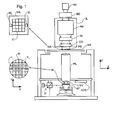
- Figure 1 schematically depicts a lithographic apparatus according to a particular embodiment of the invention.
- the apparatus comprises:
- the apparatus is of a transmissive type (e.g. employing a transmissive mask).
- the apparatus may be of a reflective type (e.g. employing a programmable mirror array of a type as referred to above).
- the illuminator IL receives a beam of radiation from a radiation source SO.
- the source and the lithographic apparatus may be separate entities, for example when the source is an excimer laser. In such cases, the source is not considered to form part of the lithographic apparatus and the radiation beam is passed from the source SO to the illuminator IL with the aid of a beam delivery system BD comprising for example suitable directing mirrors and/or a beam expander. In other cases the source may be integral part of the apparatus, for example when the source is a mercury lamp.
- the source SO and the illuminator IL, together with the beam delivery system BD if required, may be referred to as a radiation system.
- the illuminator IL may comprise adjusting means AM for adjusting the angular intensity distribution of the beam.
- adjusting means AM for adjusting the angular intensity distribution of the beam.
- the illuminator IL generally comprises various other components, such as an integrator IN and a condenser CO.
- the illuminator provides a conditioned beam of radiation, referred to as the projection beam PB, having a desired uniformity and intensity distribution in its cross-section.
- the projection beam PB is incident on the mask MA, which is held on the mask table MT. Having traversed the mask MA, the projection beam PB passes through the lens PL, which focuses the beam onto a target portion C of the substrate W.
- the substrate table WT can be moved accurately, e.g. so as to position different target portions C in the path of the beam PB.
- the first positioning means and another position sensor (which is not explicitly depicted in Figure 1) can be used to accurately position the mask MA with respect to the path of the beam PB, e.g. after mechanical retrieval from a mask library, or during a scan.
- the mask table MT may be connected to a short stroke actuator only, or may be fixed.
- Mask MA and substrate W may be aligned using mask alignment marks M1, M2 and substrate alignment marks P1, P2.
- the apparatus is provided with at least one active drying station ADS.
- the active drying station ADS is positioned as close as possible to the projection system PL and the liquid supply system LSS which is positioned under the projection system PL.
- active drying it is meant that positive measures are taken to remove liquid from an object rather than just performing normal operations on the object during which liquid may evaporate or run off naturally and not applying any measures to the object with the specific aim of drying the object.
- the liquid supply system LSS may be of any type including a localized area liquid supply system which provides liquid to a localized area of the substrate as well as to baths in which the whole of the substrate is immersed etc..
- the substrate W When the substrate W is first moved from under the projection system PL away from the liquid supply system LSS (for example when it is lifted out of a liquid supply system in the form of a bath or when water is drained from that bath) the substrate is taken to the active drying station ADS.
- the active drying station ADS Immersion liquid which remains on the substrate W is actively removed by one or a combination of the measures described below.
- the resist radiation sensitive coating on the substrate is not effected or removed by the active drying station ADS.
- the active drying station ADS will be described in relation to removing liquid from the substrate W, the active drying station may also be used for removing immersion liquid from sensors (which may be positioned on the substrate table WT and whose performance will be enhanced by removal of liquid) as well as from the substrate table itself. It may be used to remove liquid from other objects too. In the case of sensors, the liquid can be advantageously removed prior to measurement i.e. before exposure of the substrate W.
- the active drying station ADS is preferably positioned such that the substrate can be dried within a predetermined time after exposure of the substrate.
- the predetermined time is preferably less than 5 seconds more preferably less than 2 seconds and most preferably less than 1 second.
- the humidity in the apparatus it is disadvantageous for the humidity in the apparatus to be high so that it is advantageous to remove immersion liquid remaining on the substrate table and sensors etc.
- All of these functions can be performed by the active drying station ADS, preparably positioned in and/or part of the lithographic projection apparatus. Removal of remaining liquid from the sensors means that liquid cannot disturb proper leveling of the subsequent substrate, which has previously been a problem.
- the active drying station ADS may be provided with a baffle or other suitable means to fully enclose the object as it is being dried.
- a baffle or other suitable means to fully enclose the object as it is being dried.
- the whole of the top surface of the substrate table WT may be enclosed with a curtain or baffle in the active drying station ADS to substantially prevent the spread of immersion liquid around the apparatus.
- a tray could be used to catch any drips.
- the active drying station ADS has been illustrated in Figure 1 as being part of the lithographic apparatus, this is not necessarily the case, and the active drying station ADS may be positioned anywhere between the position at which the substrate W is exposed to the projection beam PB and before a substrate post exposure processing module at which various processing steps such as baking of the photoresist and development and, etching and deposition are performed.
- the active drying station may therefore be external of the lithographic projection apparatus.
- the active drying station ADS can make use of any means to remove liquid from the substrate W. Preferably the drying is achieved without substantial heating of the substrate W as this could unbalance the apparatus due to the generation of thermal gradients.
- the active drying station ADS removes liquid from the substrate W are described below. These methods may be used singly or in combination, either at the same time or one after another, as is appropriate.
- the active drying station ADS is positioned within the lithographic projection apparatus and the substrate table transports the substrate (or other object) which is to be dried to the active drying station ADS and supports the substrate/object during active removal of immersion liquid from the object by the active drying station ADS.
- the substrate table transports the substrate (or other object) which is to be dried to the active drying station ADS and supports the substrate/object during active removal of immersion liquid from the object by the active drying station ADS.
- the active drying station ADS comprises a gas flow means 10 for creating a flow of gas over the surface of the substrate W.
- a flow rate of gas of at least 50 liters per minute, more preferably at least 100 liters per minute is achievable.
- the gas is preferably filtered and/or dried prior to being blown onto the substrate W to avoid contamination of the surface of the substrate W if this is compatible with the resist (which is not the case for some resists used for 248 nm radiation).
- the gas flow means comprises an inlet 50 and an outlet 60. Gas under pressure is provided through inlet 50 and removed by an under pressure in outlet 60.
- the arrangement illustrated in Figure 2 is a so-called gas knife in which the inlet 50 is a nozzle which accelerates the gas towards the substrate W so that it impinges on the substrate at both a high flow rate and a high velocity.
- the gas jet impinges on the substrate at an acute angle to the substrate W in a direction towards the outlet 60.
- Such an arrangement is particularly effective at removing liquid from the surface of the substrate W.
- the gas flow means 10 may comprise only a single inlet 50 or a single outlet 60 or may comprise a plurality of in and outlets 50, 60.
- the substrate W may be moved under stationary in and outlet(s) 50, 60 as indicated by arrow 15.
- the in and outlets 50, 60 may also be a continuous groove as well as discrete in and outlet ports.
- the in and outlets 50, 60 may also be moveable.
- the gas flow means only to comprise an outlet 60 which is connected to a under pressure. In this case gas as well as immersion fluid on top of the substrate W will be sucked up through the outlet 60.
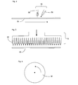
- the gas flow means 10 comprises a plurality of inlets 50 and no outlets above the substrate though outlets may need to be provided elsewhere to drain off the excess gas.
- This is a so-called shower head.
- the shower head comprises at least ten inlets 50.
- the shower head may be of a cross-sectional area which is large enough to cover the whole of the surface of the substrate W or the substrate W may be moved under the shower head 10 as it dries.
- the active drying station is dimensioned to be as long as the substrate table so that all objects on the substrate table WT (including the substrate and sensor(s)) can be dried in one go.
- filtered gas is used in the shower head 60.
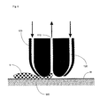
- FIG. 5 A particularly effective form of gas knife for removing liquid from the substrate W or sensor(s) is shown in Figure 5.
- the immersion liquid 5 is sucked up a central passage 110 which is connected to an under pressure.
- the passage 110 is preferably in the form of a slot (extending in and out of the page).
- Gas is supplied from outer passages 120 either side of the central passage. These outer passages 120 may also be slots.
- the outer passages may be directed at their outlet at an angle to the surface of the substrate away from perpendicular and towards the inlet of the central passage 110.
- the bottom surface of the gas knife in which outlets and inlets of the passages 110, 120 are formed may be contoured so that gas flow from outer passages 120 to the central passage 110 is smooth e.g. by rounding off the edges (i.e. giving a radius to the edges) of the inlet to the central passage 110 and optionally the outlets of the outer passages 120.
- the active drying station ADS is positioned and the path of the substrate table WT chosen such that the substrate table WT moves under the active drying station during the substrate table's normal movement after or before exposure (i.e. no deviation of path way is required).
- throughput penalty is minimized.
- a further system which may be used in the active drying station ADS is a spinner which is used for spinning the substrate W in the plane of the substrate W around its central point.
- a spinner which is used for spinning the substrate W in the plane of the substrate W around its central point.
- the active drying station ADS comprises a liquid retrieval means for recovering immersion fluid removed from the object being dried. This is particularly advantageous if the immersion liquid is not water.
- a further embodiment which can be used in combination with any one of the foregoing embodiments, by being positioned before or after the foregoing embodiments, is to use a drying liquid in which the immersion liquid dissolves on the surface of the substrate W. If the drying liquid in which the immersion liquid dissolves is of a type more easily removed from the surface of the substrate than the immersion liquid, this will speed up the drying process. Furthermore, by dissolving the immersion liquid, it may be possible to reduce dissolution of the photoresist or diffusion into the photoresist by careful choice of the drying liquid which is used. Thus, an immersion liquid dissolving liquid supply means is provided which can provide drying liquid, in which the immersion liquid dissolves, to the surface of the substrate W.
- the drying liquid chosen for this task is preferably more volatile than the immersion liquid such that it can be removed (i.e. evaporated) more easily than the immersion liquid.
- the liquid may be chosen such that it has a high contact angle with the substrate W so that it beads more easily than the immersion liquid on the substrate W and can therefore be removed.
- Suitable liquids are ketones or alcohols, in particular IPA (isopropylalchohol).
- the present invention has been described in relation to the substrate W being dried by the active drying station ADS whilst in position on the substrate table WT.
- it may be necessary to remove the substrate W from the substrate table WT before being dried by the active drying station ADS which as stated above, may be positioned outside of the lithographic apparatus. Indeed, even if the active drying station is positioned in the lithographic apparatus, it may be necessary for engineering issues to remove the substrate/object from the substrate table for drying by the active drying station ADS.
- Another immersion lithography solution which has been proposed is to provide the liquid supply system with a seal member which extends along at least a part of a boundary of the space between the final element of the projection system and the substrate table.
- the seal member is substantially stationary relative to the projection system in the XY plane though there may be some relative movement in the Z direction (in the direction of the optical axis).
- a seal is formed between the seal member and the surface of the substrate.
- the seal is a contactless seal such as a gas seal.
- a further immersion lithography solution with a localized liquid supply system is shown in Figure 8.
- Liquid is supplied by two groove inlets IN on either side of the projection system PL and is removed by a plurality of discrete outlets OUT arranged radially outwardly of the inlets IN.
- the inlets IN and OUT can be arranged in a plate with a hole in its center and through which the projection beam is projected.
- Liquid is supplied by one groove inlet IN on one side of the projection system PL and removed by a plurality of discrete outlets OUT on the other side of the projection system PL, causing a flow of a thin film of liquid between the projection system PL and the substrate W.
- the choice of which combination of inlet IN and outlets OUT to use can depend on the direction of movement of the substrate W (the other combination of inlet IN and outlets OUT being inactive).
- Such an apparatus is provided with two substrate tables for supporting the substrate. Leveling measurements are carried out with a substrate table at a first position, without immersion liquid, and exposure is carried out with a substrate table at a second position, where immersion liquid is present.
- the apparatus can have only one substrate table moving between the first and second positions.
- Embodiments of the present invention may be applied to any immersion lithography apparatus and any liquid supply system (including relevant parts thereof), in particular, but not exclusively, to any of those liquid supply systems mentioned above and the bath of liquid as described above.
Landscapes
- General Physics & Mathematics (AREA)
- Physics & Mathematics (AREA)
- Health & Medical Sciences (AREA)
- Engineering & Computer Science (AREA)
- Public Health (AREA)
- Environmental & Geological Engineering (AREA)
- Epidemiology (AREA)
- Toxicology (AREA)
- Atmospheric Sciences (AREA)
- Life Sciences & Earth Sciences (AREA)
- Computer Networks & Wireless Communication (AREA)
- Exposure And Positioning Against Photoresist Photosensitive Materials (AREA)
- Exposure Of Semiconductors, Excluding Electron Or Ion Beam Exposure (AREA)
- Container, Conveyance, Adherence, Positioning, Of Wafer (AREA)
Priority Applications (1)
| Application Number | Priority Date | Filing Date | Title |
|---|---|---|---|
| EP10180507A EP2267538B1 (fr) | 2004-05-18 | 2005-05-11 | Appareil lithographique |
Applications Claiming Priority (2)
| Application Number | Priority Date | Filing Date | Title |
|---|---|---|---|
| US10/847,661 US7616383B2 (en) | 2004-05-18 | 2004-05-18 | Lithographic apparatus and device manufacturing method |
| US847661 | 2004-05-18 |
Publications (1)
| Publication Number | Publication Date |
|---|---|
| EP1598705A1 true EP1598705A1 (fr) | 2005-11-23 |
Family
ID=34941237
Family Applications (2)
| Application Number | Title | Priority Date | Filing Date |
|---|---|---|---|
| EP10180507A Expired - Lifetime EP2267538B1 (fr) | 2004-05-18 | 2005-05-11 | Appareil lithographique |
| EP05252882A Withdrawn EP1598705A1 (fr) | 2004-05-18 | 2005-05-11 | Appareil lithographique et méthode de fabrication d'un dispositif |
Family Applications Before (1)
| Application Number | Title | Priority Date | Filing Date |
|---|---|---|---|
| EP10180507A Expired - Lifetime EP2267538B1 (fr) | 2004-05-18 | 2005-05-11 | Appareil lithographique |
Country Status (7)
| Country | Link |
|---|---|
| US (4) | US7616383B2 (fr) |
| EP (2) | EP2267538B1 (fr) |
| JP (3) | JP4669735B2 (fr) |
| KR (1) | KR100610646B1 (fr) |
| CN (2) | CN101587303B (fr) |
| SG (1) | SG117565A1 (fr) |
| TW (1) | TWI266964B (fr) |
Cited By (3)
| Publication number | Priority date | Publication date | Assignee | Title |
|---|---|---|---|---|
| EP1632813A2 (fr) | 2004-09-07 | 2006-03-08 | Matsushita Electric Industrial Co., Ltd. | Système d'exposition et procédé pour la formation de motifs |
| EP1739492A3 (fr) * | 2005-06-28 | 2007-04-18 | ASML Netherlands B.V. | Appareil lithographique et procédé de fabrication d'un dispositif |
| US8780321B2 (en) | 2008-12-08 | 2014-07-15 | Asml Netherlands B.V. | Lithographic apparatus and device manufacturing method |
Families Citing this family (88)
| Publication number | Priority date | Publication date | Assignee | Title |
|---|---|---|---|---|
| US9482966B2 (en) | 2002-11-12 | 2016-11-01 | Asml Netherlands B.V. | Lithographic apparatus and device manufacturing method |
| SG121819A1 (en) | 2002-11-12 | 2006-05-26 | Asml Netherlands Bv | Lithographic apparatus and device manufacturing method |
| US10503084B2 (en) | 2002-11-12 | 2019-12-10 | Asml Netherlands B.V. | Lithographic apparatus and device manufacturing method |
| SG171468A1 (en) * | 2002-12-10 | 2011-06-29 | Nikon Corp | Exposure apparatus and method for producing device |
| DE10261775A1 (de) | 2002-12-20 | 2004-07-01 | Carl Zeiss Smt Ag | Vorrichtung zur optischen Vermessung eines Abbildungssystems |
| EP2466621B1 (fr) | 2003-02-26 | 2015-04-01 | Nikon Corporation | Appareil d'exposition, procédé d'exposition et procédé de production du dispositif |
| KR101159564B1 (ko) | 2003-04-11 | 2012-06-25 | 가부시키가이샤 니콘 | 액침 리소그래피 머신에서 웨이퍼 교환동안 투영 렌즈 아래의 갭에서 액침액체를 유지하는 장치 및 방법 |
| KR20170016014A (ko) | 2003-04-11 | 2017-02-10 | 가부시키가이샤 니콘 | 액침 리소그래피에 의한 광학기기의 세정방법 |
| TWI424470B (zh) | 2003-05-23 | 2014-01-21 | 尼康股份有限公司 | A method of manufacturing an exposure apparatus and an element |
| TWI421911B (zh) | 2003-05-23 | 2014-01-01 | 尼康股份有限公司 | An exposure method, an exposure apparatus, and an element manufacturing method |
| CN100541717C (zh) | 2003-05-28 | 2009-09-16 | 株式会社尼康 | 曝光方法、曝光装置以及器件制造方法 |
| US7213963B2 (en) | 2003-06-09 | 2007-05-08 | Asml Netherlands B.V. | Lithographic apparatus and device manufacturing method |
| EP2261742A3 (fr) * | 2003-06-11 | 2011-05-25 | ASML Netherlands BV | Appareil lithographique et méthode de fabrication d'un dispositif |
| KR101520591B1 (ko) * | 2003-06-13 | 2015-05-14 | 가부시키가이샤 니콘 | 노광 방법, 기판 스테이지, 노광 장치, 및 디바이스 제조 방법 |
| TWI515770B (zh) | 2003-06-19 | 2016-01-01 | 尼康股份有限公司 | An exposure apparatus, an exposure method, and an element manufacturing method |
| WO2005006026A2 (fr) * | 2003-07-01 | 2005-01-20 | Nikon Corporation | Utilisation de fluides specifies isotopiquement comme elements optiques |
| EP2466382B1 (fr) * | 2003-07-08 | 2014-11-26 | Nikon Corporation | Table support de tranches pour lithographie en immersion |
| WO2005006416A1 (fr) | 2003-07-09 | 2005-01-20 | Nikon Corporation | Unite de liaison, appareil d'exposition, et procede de fabrication d'un dispositif |
| WO2005006418A1 (fr) | 2003-07-09 | 2005-01-20 | Nikon Corporation | Dispositif d'exposition et procede de fabrication |
| ATE513309T1 (de) * | 2003-07-09 | 2011-07-15 | Nikon Corp | Belichtungsvorrichtung und verfahren zur bauelementeherstellung |
| EP1650787A4 (fr) | 2003-07-25 | 2007-09-19 | Nikon Corp | Systeme d'inspection , dispositif d'inspection et procede de production pour systeme de projection optique |
| CN102043350B (zh) * | 2003-07-28 | 2014-01-29 | 株式会社尼康 | 曝光装置、器件制造方法、及曝光装置的控制方法 |
| EP1503244A1 (fr) | 2003-07-28 | 2005-02-02 | ASML Netherlands B.V. | Appareil de projection lithographique et méthode de fabrication d'un dispositif |
| US7779781B2 (en) | 2003-07-31 | 2010-08-24 | Asml Netherlands B.V. | Lithographic apparatus and device manufacturing method |
| KR101381563B1 (ko) * | 2003-08-21 | 2014-04-04 | 가부시키가이샤 니콘 | 노광 장치, 노광 방법 및 디바이스 제조 방법 |
| CN100407371C (zh) | 2003-08-29 | 2008-07-30 | 株式会社尼康 | 曝光装置和器件加工方法 |
| TWI263859B (en) | 2003-08-29 | 2006-10-11 | Asml Netherlands Bv | Lithographic apparatus and device manufacturing method |
| KR101523180B1 (ko) | 2003-09-03 | 2015-05-26 | 가부시키가이샤 니콘 | 액침 리소그래피용 유체를 제공하기 위한 장치 및 방법 |
| WO2005029559A1 (fr) | 2003-09-19 | 2005-03-31 | Nikon Corporation | Appareil d'insolation et procede permettant de produire un dispositif |
| KR101664642B1 (ko) | 2003-09-29 | 2016-10-11 | 가부시키가이샤 니콘 | 노광장치, 노광방법 및 디바이스 제조방법 |
| JP2005136364A (ja) | 2003-10-08 | 2005-05-26 | Zao Nikon Co Ltd | 基板搬送装置、露光装置、並びにデバイス製造方法 |
| EP1672682A4 (fr) | 2003-10-08 | 2008-10-15 | Zao Nikon Co Ltd | Appareil et procede de transport de substrat, appareil et procede d'exposition, et procede de production de dispositif |
| WO2005036621A1 (fr) | 2003-10-08 | 2005-04-21 | Zao Nikon Co., Ltd. | Appareil de transport de substrat, procede de transport de substrat, appareil d'exposition, procede d'exposition, et procede de production d'un dispositif |
| TWI598934B (zh) | 2003-10-09 | 2017-09-11 | 尼康股份有限公司 | Exposure apparatus, exposure method, and device manufacturing method |
| EP2717295B1 (fr) | 2003-12-03 | 2018-07-18 | Nikon Corporation | Appareil d'exposition, procédé d'exposition, et procédé de production d'un dispositif |
| DE602004030481D1 (de) | 2003-12-15 | 2011-01-20 | Nippon Kogaku Kk | Bühnensystem, belichtungsvorrichtung und belichtungsverfahren |
| US7589822B2 (en) | 2004-02-02 | 2009-09-15 | Nikon Corporation | Stage drive method and stage unit, exposure apparatus, and device manufacturing method |
| EP1713114B1 (fr) | 2004-02-03 | 2018-09-19 | Nikon Corporation | Appareil d'exposition et procédé de fabrication d'un dispositif |
| KR100557222B1 (ko) * | 2004-04-28 | 2006-03-07 | 동부아남반도체 주식회사 | 이머전 리소그라피 공정의 액체 제거 장치 및 방법 |
| EP1747499A2 (fr) | 2004-05-04 | 2007-01-31 | Nikon Corporation | Appareil et procede d'approvisionnement en fluide pour la lithographie par immersion |
| US7616383B2 (en) | 2004-05-18 | 2009-11-10 | Asml Netherlands B.V. | Lithographic apparatus and device manufacturing method |
| EP1774405B1 (fr) | 2004-06-04 | 2014-08-06 | Carl Zeiss SMT GmbH | Systeme permettant de mesurer la qualite d'une image d'un systeme d'imagerie optique |
| WO2005122218A1 (fr) | 2004-06-09 | 2005-12-22 | Nikon Corporation | Système d’exposition et méthode de production du dispositif |
| US7463330B2 (en) | 2004-07-07 | 2008-12-09 | Asml Netherlands B.V. | Lithographic apparatus and device manufacturing method |
| KR101433491B1 (ko) | 2004-07-12 | 2014-08-22 | 가부시키가이샤 니콘 | 노광 장치 및 디바이스 제조 방법 |
| KR20070048164A (ko) * | 2004-08-18 | 2007-05-08 | 가부시키가이샤 니콘 | 노광 장치 및 디바이스 제조 방법 |
| US7701550B2 (en) | 2004-08-19 | 2010-04-20 | Asml Netherlands B.V. | Lithographic apparatus and device manufacturing method |
| US7133114B2 (en) * | 2004-09-20 | 2006-11-07 | Asml Netherlands B.V. | Lithographic apparatus and device manufacturing method |
| US20070242248A1 (en) * | 2004-10-26 | 2007-10-18 | Nikon Corporation | Substrate processing method, exposure apparatus, and method for producing device |
| TWI436403B (zh) * | 2004-10-26 | 2014-05-01 | 尼康股份有限公司 | A cleaning method, a substrate processing method, an exposure apparatus, and an element manufacturing method |
| US7414699B2 (en) * | 2004-11-12 | 2008-08-19 | Asml Netherlands B.V. | Lithographic apparatus and device manufacturing method |
| US7362412B2 (en) * | 2004-11-18 | 2008-04-22 | International Business Machines Corporation | Method and apparatus for cleaning a semiconductor substrate in an immersion lithography system |
| JP4794232B2 (ja) * | 2004-12-06 | 2011-10-19 | 株式会社Sokudo | 基板処理装置 |
| TW200625026A (en) * | 2004-12-06 | 2006-07-16 | Nikon Corp | Substrate processing method, method of exposure, exposure device and device manufacturing method |
| JP5154007B2 (ja) | 2004-12-06 | 2013-02-27 | 株式会社Sokudo | 基板処理装置 |
| US7397533B2 (en) | 2004-12-07 | 2008-07-08 | Asml Netherlands B.V. | Lithographic apparatus and device manufacturing method |
| US7880860B2 (en) | 2004-12-20 | 2011-02-01 | Asml Netherlands B.V. | Lithographic apparatus and device manufacturing method |
| WO2006080516A1 (fr) | 2005-01-31 | 2006-08-03 | Nikon Corporation | Appareil d’exposition et methode de fabrication du dispositif |
| US8692973B2 (en) | 2005-01-31 | 2014-04-08 | Nikon Corporation | Exposure apparatus and method for producing device |
| US7282701B2 (en) | 2005-02-28 | 2007-10-16 | Asml Netherlands B.V. | Sensor for use in a lithographic apparatus |
| USRE43576E1 (en) | 2005-04-08 | 2012-08-14 | Asml Netherlands B.V. | Dual stage lithographic apparatus and device manufacturing method |
| US8236467B2 (en) | 2005-04-28 | 2012-08-07 | Nikon Corporation | Exposure method, exposure apparatus, and device manufacturing method |
| TW200710616A (en) * | 2005-07-11 | 2007-03-16 | Nikon Corp | Exposure apparatus and method for manufacturing device |
| JP2007103658A (ja) * | 2005-10-04 | 2007-04-19 | Canon Inc | 露光方法および装置ならびにデバイス製造方法 |
| US7929109B2 (en) | 2005-10-20 | 2011-04-19 | Nikon Corporation | Apparatus and method for recovering liquid droplets in immersion lithography |
| US7649611B2 (en) | 2005-12-30 | 2010-01-19 | Asml Netherlands B.V. | Lithographic apparatus and device manufacturing method |
| US8027019B2 (en) | 2006-03-28 | 2011-09-27 | Asml Netherlands B.V. | Lithographic apparatus and device manufacturing method |
| EP2037486A4 (fr) * | 2006-05-18 | 2012-01-11 | Nikon Corp | Procédé et appareil d'exposition, procédé de maintenance et procédé de fabrication de l'appareil associé |
| TW200818256A (en) * | 2006-05-22 | 2008-04-16 | Nikon Corp | Exposure method and apparatus, maintenance method, and device manufacturing method |
| EP2034515A4 (fr) * | 2006-05-23 | 2012-01-18 | Nikon Corp | Procédé de maintenance, procédé et appareil d'exposition et procédé de fabrication de dispositif |
| WO2008001871A1 (fr) * | 2006-06-30 | 2008-01-03 | Nikon Corporation | Procédé de maintenance, procédé d'exposition et procédé de fabrication d'appareil et de dispositif |
| JP4758977B2 (ja) * | 2006-12-07 | 2011-08-31 | エーエスエムエル ネザーランズ ビー.ブイ. | リソグラフィ投影装置、デバイス製造方法 |
| US9632425B2 (en) * | 2006-12-07 | 2017-04-25 | Asml Holding N.V. | Lithographic apparatus, a dryer and a method of removing liquid from a surface |
| JP2008147577A (ja) * | 2006-12-13 | 2008-06-26 | Canon Inc | 露光装置及びデバイス製造方法 |
| US8817226B2 (en) | 2007-02-15 | 2014-08-26 | Asml Holding N.V. | Systems and methods for insitu lens cleaning using ozone in immersion lithography |
| US8654305B2 (en) | 2007-02-15 | 2014-02-18 | Asml Holding N.V. | Systems and methods for insitu lens cleaning in immersion lithography |
| US20090109416A1 (en) * | 2007-09-13 | 2009-04-30 | Applied Precision, Inc. | Dispersing immersion liquid for high resolution imaging and lithography |
| NL1036631A1 (nl) * | 2008-03-24 | 2009-09-25 | Asml Netherlands Bv | Immersion Lithographic Apparatus and Device Manufacturing Method. |
| KR101448152B1 (ko) * | 2008-03-26 | 2014-10-07 | 삼성전자주식회사 | 수직 포토게이트를 구비한 거리측정 센서 및 그를 구비한입체 컬러 이미지 센서 |
| US9176393B2 (en) | 2008-05-28 | 2015-11-03 | Asml Netherlands B.V. | Lithographic apparatus and a method of operating the apparatus |
| NL2005528A (en) * | 2009-12-02 | 2011-06-07 | Asml Netherlands Bv | Lithographic apparatus and device manufacturing method. |
| NL2005717A (en) * | 2009-12-18 | 2011-06-21 | Asml Netherlands Bv | A lithographic apparatus and a device manufacturing method. |
| US9222194B2 (en) | 2010-08-19 | 2015-12-29 | International Business Machines Corporation | Rinsing and drying for electrochemical processing |
| US9570576B2 (en) * | 2013-12-10 | 2017-02-14 | Infineon Technologies Ag | Method for forming a semiconductor device having insulating parts or layers formed via anodic oxidation |
| CN111089980B (zh) * | 2013-12-13 | 2023-08-15 | 文塔纳医疗系统公司 | 生物样本的自动化组织学处理及相关的技术 |
| CN105980828B (zh) | 2013-12-13 | 2021-12-17 | 文塔纳医疗系统公司 | 用于生物标本组织处理的染色试剂和其它液体及关联技术 |
| DE112014005277T5 (de) * | 2014-06-12 | 2016-10-06 | Fuji Electric Co., Ltd. | Vorrichtung zum Einbringen von Verunreinigungen, Verfahren zum Einbringen von Verunreinigungen und Verfahren zur Herstellung eines Halbleiterelements |
| WO2015193036A1 (fr) | 2014-06-16 | 2015-12-23 | Asml Netherlands B.V. | Appareil lithographique, procédé de transfert d'un substrat et procédé de fabrication d'un dispositif |
Citations (8)
| Publication number | Priority date | Publication date | Assignee | Title |
|---|---|---|---|---|
| JPH06124873A (ja) * | 1992-10-09 | 1994-05-06 | Canon Inc | 液浸式投影露光装置 |
| EP0605103A1 (fr) * | 1992-11-27 | 1994-07-06 | Canon Kabushiki Kaisha | Dispositif de projection pour l'exposition immergée |
| WO2004053952A1 (fr) * | 2002-12-10 | 2004-06-24 | Nikon Corporation | Appareil d'exposition et procede de fabrication de ce dispositif |
| WO2004105107A1 (fr) * | 2003-05-23 | 2004-12-02 | Nikon Corporation | Dispositif d'exposition et procede de fabrication dudit dispositif |
| US20050046934A1 (en) * | 2003-08-29 | 2005-03-03 | Tokyo Electron Limited | Method and system for drying a substrate |
| WO2005022616A1 (fr) | 2003-08-29 | 2005-03-10 | Nikon Corporation | Appareil d'exposition et procede de production d'un dispositif |
| WO2005036623A1 (fr) | 2003-10-08 | 2005-04-21 | Zao Nikon Co., Ltd. | Appareil et procede de transport de substrat, appareil et procede d'exposition, et procede de production de dispositif |
| EP1717845A1 (fr) | 2004-02-19 | 2006-11-02 | Nikon Corporation | Appareil d'exposition et procede d'exposition, et procede de production de l'appareil |
Family Cites Families (221)
| Publication number | Priority date | Publication date | Assignee | Title |
|---|---|---|---|---|
| DE221563C (fr) | ||||
| DE224448C (fr) | ||||
| DE206207C (fr) | ||||
| GB1242527A (en) | 1967-10-20 | 1971-08-11 | Kodak Ltd | Optical instruments |
| US3573975A (en) | 1968-07-10 | 1971-04-06 | Ibm | Photochemical fabrication process |
| JPS5919912Y2 (ja) | 1978-08-21 | 1984-06-08 | 清水建設株式会社 | 複合熱交換器 |
| ATE1462T1 (de) | 1979-07-27 | 1982-08-15 | Werner W. Dr. Tabarelli | Optisches lithographieverfahren und einrichtung zum kopieren eines musters auf eine halbleiterscheibe. |
| FR2474708B1 (fr) | 1980-01-24 | 1987-02-20 | Dme | Procede de microphotolithographie a haute resolution de traits |
| JPS5754317A (en) | 1980-09-19 | 1982-03-31 | Hitachi Ltd | Method and device for forming pattern |
| US4509852A (en) | 1980-10-06 | 1985-04-09 | Werner Tabarelli | Apparatus for the photolithographic manufacture of integrated circuit elements |
| US4346164A (en) | 1980-10-06 | 1982-08-24 | Werner Tabarelli | Photolithographic method for the manufacture of integrated circuits |
| US4390273A (en) | 1981-02-17 | 1983-06-28 | Censor Patent-Und Versuchsanstalt | Projection mask as well as a method and apparatus for the embedding thereof and projection printing system |
| JPS57153433A (en) | 1981-03-18 | 1982-09-22 | Hitachi Ltd | Manufacturing device for semiconductor |
| JPS57153433U (fr) | 1981-03-20 | 1982-09-27 | ||
| JPS58202448A (ja) | 1982-05-21 | 1983-11-25 | Hitachi Ltd | 露光装置 |
| DD206607A1 (de) | 1982-06-16 | 1984-02-01 | Mikroelektronik Zt Forsch Tech | Verfahren und vorrichtung zur beseitigung von interferenzeffekten |
| JPS5919912A (ja) | 1982-07-26 | 1984-02-01 | Hitachi Ltd | 液浸距離保持装置 |
| DD242880A1 (de) | 1983-01-31 | 1987-02-11 | Kuch Karl Heinz | Einrichtung zur fotolithografischen strukturuebertragung |
| DD221563A1 (de) | 1983-09-14 | 1985-04-24 | Mikroelektronik Zt Forsch Tech | Immersionsobjektiv fuer die schrittweise projektionsabbildung einer maskenstruktur |
| DD224448A1 (de) | 1984-03-01 | 1985-07-03 | Zeiss Jena Veb Carl | Einrichtung zur fotolithografischen strukturuebertragung |
| JPS61113376A (ja) | 1984-11-07 | 1986-05-31 | Sony Corp | テレビジヨン信号の動き検出装置 |
| JPS6265326A (ja) | 1985-09-18 | 1987-03-24 | Hitachi Ltd | 露光装置 |
| JPS6265326U (fr) | 1985-10-16 | 1987-04-23 | ||
| JPS62121417A (ja) | 1985-11-22 | 1987-06-02 | Hitachi Ltd | 液浸対物レンズ装置 |
| JPS62121417U (fr) | 1986-01-24 | 1987-08-01 | ||
| JPS62188322A (ja) * | 1986-02-14 | 1987-08-17 | Hitachi Micro Comput Eng Ltd | 洗浄装置 |
| JPS63157419A (ja) | 1986-12-22 | 1988-06-30 | Toshiba Corp | 微細パタ−ン転写装置 |
| JPS63157419U (fr) | 1987-03-31 | 1988-10-14 | ||
| US5040020A (en) | 1988-03-31 | 1991-08-13 | Cornell Research Foundation, Inc. | Self-aligned, high resolution resonant dielectric lithography |
| JPH03209479A (ja) | 1989-09-06 | 1991-09-12 | Sanee Giken Kk | 露光方法 |
| JPH04305915A (ja) | 1991-04-02 | 1992-10-28 | Nikon Corp | 密着型露光装置 |
| JPH04305917A (ja) | 1991-04-02 | 1992-10-28 | Nikon Corp | 密着型露光装置 |
| JPH0562877A (ja) | 1991-09-02 | 1993-03-12 | Yasuko Shinohara | 光によるlsi製造縮小投影露光装置の光学系 |
| JP2520833B2 (ja) | 1992-12-21 | 1996-07-31 | 東京エレクトロン株式会社 | 浸漬式の液処理装置 |
| JPH07220990A (ja) | 1994-01-28 | 1995-08-18 | Hitachi Ltd | パターン形成方法及びその露光装置 |
| JPH08316125A (ja) | 1995-05-19 | 1996-11-29 | Hitachi Ltd | 投影露光方法及び露光装置 |
| JPH08316124A (ja) | 1995-05-19 | 1996-11-29 | Hitachi Ltd | 投影露光方法及び露光装置 |
| JPH09283401A (ja) | 1996-04-09 | 1997-10-31 | Nikon Corp | 露光装置 |
| US6104687A (en) | 1996-08-26 | 2000-08-15 | Digital Papyrus Corporation | Method and apparatus for coupling an optical lens to a disk through a coupling medium having a relatively high index of refraction |
| US5825043A (en) | 1996-10-07 | 1998-10-20 | Nikon Precision Inc. | Focusing and tilting adjustment system for lithography aligner, manufacturing apparatus or inspection apparatus |
| JP3511441B2 (ja) * | 1996-11-29 | 2004-03-29 | 忠弘 大見 | 洗浄やエッチング、現像、剥離等を含むウエット処理に用いる省液型の液体供給ノズル、ウエット処理装置及びウエット処理方法 |
| JPH1133506A (ja) * | 1997-07-24 | 1999-02-09 | Tadahiro Omi | 流体処理装置及び洗浄処理システム |
| JP3612920B2 (ja) | 1997-02-14 | 2005-01-26 | ソニー株式会社 | 光学記録媒体の原盤作製用露光装置 |
| JPH10255319A (ja) | 1997-03-12 | 1998-09-25 | Hitachi Maxell Ltd | 原盤露光装置及び方法 |
| JP3070511B2 (ja) * | 1997-03-31 | 2000-07-31 | 日本電気株式会社 | 基板乾燥装置 |
| JP3747566B2 (ja) | 1997-04-23 | 2006-02-22 | 株式会社ニコン | 液浸型露光装置 |
| JP3817836B2 (ja) | 1997-06-10 | 2006-09-06 | 株式会社ニコン | 露光装置及びその製造方法並びに露光方法及びデバイス製造方法 |
| US5900354A (en) | 1997-07-03 | 1999-05-04 | Batchelder; John Samuel | Method for optical inspection and lithography |
| JPH11283903A (ja) | 1998-03-30 | 1999-10-15 | Nikon Corp | 投影光学系検査装置及び同装置を備えた投影露光装置 |
| WO1999027568A1 (fr) | 1997-11-21 | 1999-06-03 | Nikon Corporation | Graveur de motifs a projection et procede de sensibilisation a projection |
| JPH11176727A (ja) | 1997-12-11 | 1999-07-02 | Nikon Corp | 投影露光装置 |
| EP1039511A4 (fr) | 1997-12-12 | 2005-03-02 | Nikon Corp | Procede d'exposition par projection et graveur a projection |
| WO1999049504A1 (fr) | 1998-03-26 | 1999-09-30 | Nikon Corporation | Procede et systeme d'exposition par projection |
| JP2000058436A (ja) | 1998-08-11 | 2000-02-25 | Nikon Corp | 投影露光装置及び露光方法 |
| US6254936B1 (en) * | 1998-09-14 | 2001-07-03 | Silicon Valley Group, Inc. | Environment exchange control for material on a wafer surface |
| TWI242111B (en) | 1999-04-19 | 2005-10-21 | Asml Netherlands Bv | Gas bearings for use in vacuum chambers and their application in lithographic projection apparatus |
| JP4504479B2 (ja) | 1999-09-21 | 2010-07-14 | オリンパス株式会社 | 顕微鏡用液浸対物レンズ |
| US6995930B2 (en) | 1999-12-29 | 2006-02-07 | Carl Zeiss Smt Ag | Catadioptric projection objective with geometric beam splitting |
| US7187503B2 (en) | 1999-12-29 | 2007-03-06 | Carl Zeiss Smt Ag | Refractive projection objective for immersion lithography |
| JP4122674B2 (ja) | 2000-02-14 | 2008-07-23 | 株式会社日立ハイテクノロジーズ | 基板乾燥装置及び乾燥方法 |
| US6421932B2 (en) * | 2000-02-14 | 2002-07-23 | Hitachi Electronics Engineering Co., Ltd. | Method and apparatus for drying substrate plates |
| JP2001272604A (ja) | 2000-03-27 | 2001-10-05 | Olympus Optical Co Ltd | 液浸対物レンズおよびそれを用いた光学装置 |
| JP2002016124A (ja) | 2000-06-28 | 2002-01-18 | Sony Corp | ウェーハ搬送アーム機構 |
| US7234477B2 (en) * | 2000-06-30 | 2007-06-26 | Lam Research Corporation | Method and apparatus for drying semiconductor wafer surfaces using a plurality of inlets and outlets held in close proximity to the wafer surfaces |
| TW591653B (en) | 2000-08-08 | 2004-06-11 | Koninkl Philips Electronics Nv | Method of manufacturing an optically scannable information carrier |
| KR100866818B1 (ko) | 2000-12-11 | 2008-11-04 | 가부시키가이샤 니콘 | 투영광학계 및 이 투영광학계를 구비한 노광장치 |
| JP4189141B2 (ja) * | 2000-12-21 | 2008-12-03 | 株式会社東芝 | 基板処理装置及びこれを用いた基板処理方法 |
| JP2002289575A (ja) * | 2001-03-28 | 2002-10-04 | Dainippon Screen Mfg Co Ltd | 基板処理方法及びその装置 |
| WO2002091078A1 (fr) | 2001-05-07 | 2002-11-14 | Massachusetts Institute Of Technology | Procedes et appareil utilisant un support d'adaptation d'indice |
| JP4040270B2 (ja) * | 2001-06-25 | 2008-01-30 | 東京エレクトロン株式会社 | 基板の処理装置 |
| US6810109B2 (en) | 2001-07-13 | 2004-10-26 | Medtronic Ave, Inc. | X-ray emitting system and method |
| JP3886424B2 (ja) * | 2001-08-28 | 2007-02-28 | 鹿児島日本電気株式会社 | 基板処理装置及び方法 |
| US6600547B2 (en) | 2001-09-24 | 2003-07-29 | Nikon Corporation | Sliding seal |
| EP1446703A2 (fr) | 2001-11-07 | 2004-08-18 | Applied Materials, Inc. | Imprimante a matrice en grille de points optique |
| JP2003178943A (ja) * | 2001-12-10 | 2003-06-27 | Tokyo Electron Ltd | 現像処理方法及び現像処理装置 |
| US7092069B2 (en) | 2002-03-08 | 2006-08-15 | Carl Zeiss Smt Ag | Projection exposure method and projection exposure system |
| DE10210899A1 (de) | 2002-03-08 | 2003-09-18 | Zeiss Carl Smt Ag | Refraktives Projektionsobjektiv für Immersions-Lithographie |
| DE10229818A1 (de) | 2002-06-28 | 2004-01-15 | Carl Zeiss Smt Ag | Verfahren zur Fokusdetektion und Abbildungssystem mit Fokusdetektionssystem |
| JP3806670B2 (ja) | 2002-06-12 | 2006-08-09 | 住友金属建材株式会社 | 土留め用かご枠の連結部材 |
| JP2005536775A (ja) | 2002-08-23 | 2005-12-02 | 株式会社ニコン | 投影光学系、フォトリソグラフィ方法および露光装置、並びに露光装置を用いた方法 |
| US6988326B2 (en) | 2002-09-30 | 2006-01-24 | Lam Research Corporation | Phobic barrier meniscus separation and containment |
| US7367345B1 (en) * | 2002-09-30 | 2008-05-06 | Lam Research Corporation | Apparatus and method for providing a confined liquid for immersion lithography |
| US6954993B1 (en) | 2002-09-30 | 2005-10-18 | Lam Research Corporation | Concentric proximity processing head |
| US7093375B2 (en) | 2002-09-30 | 2006-08-22 | Lam Research Corporation | Apparatus and method for utilizing a meniscus in substrate processing |
| US6788477B2 (en) | 2002-10-22 | 2004-09-07 | Taiwan Semiconductor Manufacturing Co., Ltd. | Apparatus for method for immersion lithography |
| CN101382738B (zh) | 2002-11-12 | 2011-01-12 | Asml荷兰有限公司 | 光刻投射装置 |
| US7110081B2 (en) | 2002-11-12 | 2006-09-19 | Asml Netherlands B.V. | Lithographic apparatus and device manufacturing method |
| KR100585476B1 (ko) * | 2002-11-12 | 2006-06-07 | 에이에스엠엘 네델란즈 비.브이. | 리소그래피 장치 및 디바이스 제조방법 |
| SG121819A1 (en) * | 2002-11-12 | 2006-05-26 | Asml Netherlands Bv | Lithographic apparatus and device manufacturing method |
| US6829035B2 (en) * | 2002-11-12 | 2004-12-07 | Applied Materials Israel, Ltd. | Advanced mask cleaning and handling |
| EP1420299B1 (fr) | 2002-11-12 | 2011-01-05 | ASML Netherlands B.V. | Appareil lithographique à immersion et méthode de fabrication d'un dispositif |
| DE60335595D1 (de) * | 2002-11-12 | 2011-02-17 | Asml Netherlands Bv | Lithographischer Apparat mit Immersion und Verfahren zur Herstellung einer Vorrichtung |
| SG121822A1 (en) * | 2002-11-12 | 2006-05-26 | Asml Netherlands Bv | Lithographic apparatus and device manufacturing method |
| SG131766A1 (en) * | 2002-11-18 | 2007-05-28 | Asml Netherlands Bv | Lithographic apparatus and device manufacturing method |
| DE10253679A1 (de) | 2002-11-18 | 2004-06-03 | Infineon Technologies Ag | Optische Einrichtung zur Verwendung bei einem Lithographie-Verfahren, insbesondere zur Herstellung eines Halbleiter-Bauelements, sowie optisches Lithographieverfahren |
| TWI255971B (en) * | 2002-11-29 | 2006-06-01 | Asml Netherlands Bv | Lithographic apparatus and device manufacturing method |
| DE10258718A1 (de) | 2002-12-09 | 2004-06-24 | Carl Zeiss Smt Ag | Projektionsobjektiv, insbesondere für die Mikrolithographie, sowie Verfahren zur Abstimmung eines Projektionsobjektives |
| JP4352874B2 (ja) | 2002-12-10 | 2009-10-28 | 株式会社ニコン | 露光装置及びデバイス製造方法 |
| EP1571695A4 (fr) | 2002-12-10 | 2008-10-15 | Nikon Corp | Appareil d'exposition et son procede de fabrication |
| JP4525062B2 (ja) * | 2002-12-10 | 2010-08-18 | 株式会社ニコン | 露光装置及びデバイス製造方法、露光システム |
| AU2003302831A1 (en) | 2002-12-10 | 2004-06-30 | Nikon Corporation | Exposure method, exposure apparatus and method for manufacturing device |
| KR101157002B1 (ko) | 2002-12-10 | 2012-06-21 | 가부시키가이샤 니콘 | 노광 장치 및 디바이스 제조 방법 |
| CN101872135B (zh) | 2002-12-10 | 2013-07-31 | 株式会社尼康 | 曝光设备和器件制造法 |
| AU2003289271A1 (en) | 2002-12-10 | 2004-06-30 | Nikon Corporation | Exposure apparatus, exposure method and method for manufacturing device |
| JP4232449B2 (ja) | 2002-12-10 | 2009-03-04 | 株式会社ニコン | 露光方法、露光装置、及びデバイス製造方法 |
| AU2003289272A1 (en) | 2002-12-10 | 2004-06-30 | Nikon Corporation | Surface position detection apparatus, exposure method, and device porducing method |
| EP1571700A4 (fr) | 2002-12-10 | 2007-09-12 | Nikon Corp | Dispositif optique et appareil de projection d'ambiance utilisant un tel dispositif optique |
| EP1429190B1 (fr) | 2002-12-10 | 2012-05-09 | Canon Kabushiki Kaisha | Appareil et méthode d'exposition |
| EP1571701A4 (fr) | 2002-12-10 | 2008-04-09 | Nikon Corp | Appareil d'exposition et procede de fabrication du dispositif |
| DE10257766A1 (de) | 2002-12-10 | 2004-07-15 | Carl Zeiss Smt Ag | Verfahren zur Einstellung einer gewünschten optischen Eigenschaft eines Projektionsobjektivs sowie mikrolithografische Projektionsbelichtungsanlage |
| ATE424026T1 (de) | 2002-12-13 | 2009-03-15 | Koninkl Philips Electronics Nv | Flüssigkeitsentfernung in einem verfahren und einer einrichtung zum bestrahlen von flecken auf einer schicht |
| EP1732075A3 (fr) | 2002-12-19 | 2007-02-21 | Koninklijke Philips Electronics N.V. | Procédé et dispositif pour irradier des points sur une couche |
| US7010958B2 (en) | 2002-12-19 | 2006-03-14 | Asml Holding N.V. | High-resolution gas gauge proximity sensor |
| USRE48515E1 (en) | 2002-12-19 | 2021-04-13 | Asml Netherlands B.V. | Method and device for irradiating spots on a layer |
| US6781670B2 (en) | 2002-12-30 | 2004-08-24 | Intel Corporation | Immersion lithography |
| US7090964B2 (en) | 2003-02-21 | 2006-08-15 | Asml Holding N.V. | Lithographic printing with polarized light |
| US7206059B2 (en) | 2003-02-27 | 2007-04-17 | Asml Netherlands B.V. | Stationary and dynamic radial transverse electric polarizer for high numerical aperture systems |
| US6943941B2 (en) | 2003-02-27 | 2005-09-13 | Asml Netherlands B.V. | Stationary and dynamic radial transverse electric polarizer for high numerical aperture systems |
| US7029832B2 (en) | 2003-03-11 | 2006-04-18 | Samsung Electronics Co., Ltd. | Immersion lithography methods using carbon dioxide |
| US20050164522A1 (en) | 2003-03-24 | 2005-07-28 | Kunz Roderick R. | Optical fluids, and systems and methods of making and using the same |
| WO2004093159A2 (fr) | 2003-04-09 | 2004-10-28 | Nikon Corporation | Systeme de regulation des fluides pour lithographie par immersion |
| EP2921905B1 (fr) | 2003-04-10 | 2017-12-27 | Nikon Corporation | Trajet d'écoulement permettant de recueillir un liquide pour un appareil de lithographie par immersion |
| KR101177330B1 (ko) * | 2003-04-10 | 2012-08-30 | 가부시키가이샤 니콘 | 액침 리소그래피 장치 |
| WO2004090634A2 (fr) | 2003-04-10 | 2004-10-21 | Nikon Corporation | Systeme ambiant a piegeage de vide pour un appareil de lithographie a immersion |
| JP4656057B2 (ja) | 2003-04-10 | 2011-03-23 | 株式会社ニコン | 液浸リソグラフィ装置用電気浸透素子 |
| KR20170016014A (ko) | 2003-04-11 | 2017-02-10 | 가부시키가이샤 니콘 | 액침 리소그래피에 의한 광학기기의 세정방법 |
| KR101159564B1 (ko) | 2003-04-11 | 2012-06-25 | 가부시키가이샤 니콘 | 액침 리소그래피 머신에서 웨이퍼 교환동안 투영 렌즈 아래의 갭에서 액침액체를 유지하는 장치 및 방법 |
| WO2004092830A2 (fr) | 2003-04-11 | 2004-10-28 | Nikon Corporation | Systeme de projection et de recuperation de liquides pour lithographie par immersion |
| ATE542167T1 (de) | 2003-04-17 | 2012-02-15 | Nikon Corp | Lithographisches immersionsgerät |
| JP4146755B2 (ja) | 2003-05-09 | 2008-09-10 | 松下電器産業株式会社 | パターン形成方法 |
| JP4025683B2 (ja) | 2003-05-09 | 2007-12-26 | 松下電器産業株式会社 | パターン形成方法及び露光装置 |
| TWI295414B (en) | 2003-05-13 | 2008-04-01 | Asml Netherlands Bv | Lithographic apparatus and device manufacturing method |
| CN100437358C (zh) | 2003-05-15 | 2008-11-26 | 株式会社尼康 | 曝光装置及器件制造方法 |
| CN1307456C (zh) | 2003-05-23 | 2007-03-28 | 佳能株式会社 | 投影光学系统、曝光装置及器件的制造方法 |
| JP2005277363A (ja) * | 2003-05-23 | 2005-10-06 | Nikon Corp | 露光装置及びデバイス製造方法 |
| TW594841B (en) * | 2003-05-28 | 2004-06-21 | Au Optronics Corp | Apparatus and method for preventing contamination of substrate from condensate liquid |
| EP2261742A3 (fr) | 2003-06-11 | 2011-05-25 | ASML Netherlands BV | Appareil lithographique et méthode de fabrication d'un dispositif |
| JP4084710B2 (ja) | 2003-06-12 | 2008-04-30 | 松下電器産業株式会社 | パターン形成方法 |
| JP4054285B2 (ja) | 2003-06-12 | 2008-02-27 | 松下電器産業株式会社 | パターン形成方法 |
| US6867844B2 (en) * | 2003-06-19 | 2005-03-15 | Asml Holding N.V. | Immersion photolithography system and method using microchannel nozzles |
| JP4084712B2 (ja) | 2003-06-23 | 2008-04-30 | 松下電器産業株式会社 | パターン形成方法 |
| JP4029064B2 (ja) | 2003-06-23 | 2008-01-09 | 松下電器産業株式会社 | パターン形成方法 |
| US6809794B1 (en) | 2003-06-27 | 2004-10-26 | Asml Holding N.V. | Immersion photolithography system and method using inverted wafer-projection optics interface |
| EP1498778A1 (fr) | 2003-06-27 | 2005-01-19 | ASML Netherlands B.V. | Appareil lithographique et méthode de fabrication d'un dispositif |
| WO2005006026A2 (fr) | 2003-07-01 | 2005-01-20 | Nikon Corporation | Utilisation de fluides specifies isotopiquement comme elements optiques |
| EP2466382B1 (fr) * | 2003-07-08 | 2014-11-26 | Nikon Corporation | Table support de tranches pour lithographie en immersion |
| SG109000A1 (en) * | 2003-07-16 | 2005-02-28 | Asml Netherlands Bv | Lithographic apparatus and device manufacturing method |
| US7384149B2 (en) | 2003-07-21 | 2008-06-10 | Asml Netherlands B.V. | Lithographic projection apparatus, gas purging method and device manufacturing method and purge gas supply system |
| US7006209B2 (en) | 2003-07-25 | 2006-02-28 | Advanced Micro Devices, Inc. | Method and apparatus for monitoring and controlling imaging in immersion lithography systems |
| US7326522B2 (en) * | 2004-02-11 | 2008-02-05 | Asml Netherlands B.V. | Device manufacturing method and a substrate |
| US7175968B2 (en) | 2003-07-28 | 2007-02-13 | Asml Netherlands B.V. | Lithographic apparatus, device manufacturing method and a substrate |
| US7579135B2 (en) | 2003-08-11 | 2009-08-25 | Taiwan Semiconductor Manufacturing Company, Ltd. | Lithography apparatus for manufacture of integrated circuits |
| US7700267B2 (en) | 2003-08-11 | 2010-04-20 | Taiwan Semiconductor Manufacturing Company, Ltd. | Immersion fluid for immersion lithography, and method of performing immersion lithography |
| US7061578B2 (en) | 2003-08-11 | 2006-06-13 | Advanced Micro Devices, Inc. | Method and apparatus for monitoring and controlling imaging in immersion lithography systems |
| US7085075B2 (en) | 2003-08-12 | 2006-08-01 | Carl Zeiss Smt Ag | Projection objectives including a plurality of mirrors with lenses ahead of mirror M3 |
| US6844206B1 (en) | 2003-08-21 | 2005-01-18 | Advanced Micro Devices, Llp | Refractive index system monitor and control for immersion lithography |
| JP4305095B2 (ja) * | 2003-08-29 | 2009-07-29 | 株式会社ニコン | 光学部品の洗浄機構を搭載した液浸投影露光装置及び液浸光学部品洗浄方法 |
| US6954256B2 (en) | 2003-08-29 | 2005-10-11 | Asml Netherlands B.V. | Gradient immersion lithography |
| US7014966B2 (en) | 2003-09-02 | 2006-03-21 | Advanced Micro Devices, Inc. | Method and apparatus for elimination of bubbles in immersion medium in immersion lithography systems |
| KR101523180B1 (ko) | 2003-09-03 | 2015-05-26 | 가부시키가이샤 니콘 | 액침 리소그래피용 유체를 제공하기 위한 장치 및 방법 |
| JP3870182B2 (ja) | 2003-09-09 | 2007-01-17 | キヤノン株式会社 | 露光装置及びデバイス製造方法 |
| US6961186B2 (en) | 2003-09-26 | 2005-11-01 | Takumi Technology Corp. | Contact printing using a magnified mask image |
| US7369217B2 (en) | 2003-10-03 | 2008-05-06 | Micronic Laser Systems Ab | Method and device for immersion lithography |
| WO2005036621A1 (fr) | 2003-10-08 | 2005-04-21 | Zao Nikon Co., Ltd. | Appareil de transport de substrat, procede de transport de substrat, appareil d'exposition, procede d'exposition, et procede de production d'un dispositif |
| US7678527B2 (en) | 2003-10-16 | 2010-03-16 | Intel Corporation | Methods and compositions for providing photoresist with improved properties for contacting liquids |
| WO2005050324A2 (fr) | 2003-11-05 | 2005-06-02 | Dsm Ip Assets B.V. | Procede et appareil de production de microcircuits |
| US7924397B2 (en) | 2003-11-06 | 2011-04-12 | Taiwan Semiconductor Manufacturing Company, Ltd. | Anti-corrosion layer on objective lens for liquid immersion lithography applications |
| US8854602B2 (en) | 2003-11-24 | 2014-10-07 | Asml Netherlands B.V. | Holding device for an optical element in an objective |
| US7545481B2 (en) | 2003-11-24 | 2009-06-09 | Asml Netherlands B.V. | Lithographic apparatus and device manufacturing method |
| US7125652B2 (en) | 2003-12-03 | 2006-10-24 | Advanced Micro Devices, Inc. | Immersion lithographic process using a conforming immersion medium |
| JP2007516613A (ja) | 2003-12-15 | 2007-06-21 | カール・ツアイス・エスエムテイ・アーゲー | 少なくとも1つの液体レンズを備えるマイクロリソグラフィー投影対物レンズとしての対物レンズ |
| JP5106858B2 (ja) | 2003-12-15 | 2012-12-26 | カール・ツァイス・エスエムティー・ゲーエムベーハー | 高開口数と平面状端面とを有する投影対物レンズ |
| US20050185269A1 (en) | 2003-12-19 | 2005-08-25 | Carl Zeiss Smt Ag | Catadioptric projection objective with geometric beam splitting |
| US7460206B2 (en) | 2003-12-19 | 2008-12-02 | Carl Zeiss Smt Ag | Projection objective for immersion lithography |
| WO2005059645A2 (fr) | 2003-12-19 | 2005-06-30 | Carl Zeiss Smt Ag | Objectif de projection de microlithographie comprenant des éléments cristallins |
| JP2005183656A (ja) | 2003-12-19 | 2005-07-07 | Canon Inc | 露光装置 |
| JP2005183744A (ja) * | 2003-12-22 | 2005-07-07 | Nikon Corp | 露光装置及びデバイス製造方法 |
| US7394521B2 (en) | 2003-12-23 | 2008-07-01 | Asml Netherlands B.V. | Lithographic apparatus and device manufacturing method |
| US7589818B2 (en) * | 2003-12-23 | 2009-09-15 | Asml Netherlands B.V. | Lithographic apparatus, alignment apparatus, device manufacturing method, and a method of converting an apparatus |
| US7119884B2 (en) | 2003-12-24 | 2006-10-10 | Asml Netherlands B.V. | Lithographic apparatus and device manufacturing method |
| US20050147920A1 (en) | 2003-12-30 | 2005-07-07 | Chia-Hui Lin | Method and system for immersion lithography |
| US7088422B2 (en) | 2003-12-31 | 2006-08-08 | International Business Machines Corporation | Moving lens for immersion optical lithography |
| US7145641B2 (en) * | 2003-12-31 | 2006-12-05 | Asml Netherlands, B.V. | Lithographic apparatus, device manufacturing method, and device manufactured thereby |
| JP4371822B2 (ja) | 2004-01-06 | 2009-11-25 | キヤノン株式会社 | 露光装置 |
| JP4429023B2 (ja) | 2004-01-07 | 2010-03-10 | キヤノン株式会社 | 露光装置及びデバイス製造方法 |
| JP4194495B2 (ja) | 2004-01-07 | 2008-12-10 | 東京エレクトロン株式会社 | 塗布・現像装置 |
| US20050153424A1 (en) | 2004-01-08 | 2005-07-14 | Derek Coon | Fluid barrier with transparent areas for immersion lithography |
| KR101407204B1 (ko) | 2004-01-14 | 2014-06-13 | 칼 짜이스 에스엠티 게엠베하 | 투영 대물렌즈 |
| CN101793993B (zh) | 2004-01-16 | 2013-04-03 | 卡尔蔡司Smt有限责任公司 | 光学元件、光学布置及系统 |
| WO2005069078A1 (fr) | 2004-01-19 | 2005-07-28 | Carl Zeiss Smt Ag | Dispositif d'exposition par projection microlithographique avec objectif de projection par immersion |
| CN1938646B (zh) | 2004-01-20 | 2010-12-15 | 卡尔蔡司Smt股份公司 | 曝光装置和用于投影透镜的测量装置 |
| US7026259B2 (en) | 2004-01-21 | 2006-04-11 | International Business Machines Corporation | Liquid-filled balloons for immersion lithography |
| US7391501B2 (en) | 2004-01-22 | 2008-06-24 | Intel Corporation | Immersion liquids with siloxane polymer for immersion lithography |
| JP2007520893A (ja) | 2004-02-03 | 2007-07-26 | ロチェスター インスティテュート オブ テクノロジー | 流体を使用したフォトリソグラフィ法及びそのシステム |
| EP1713114B1 (fr) * | 2004-02-03 | 2018-09-19 | Nikon Corporation | Appareil d'exposition et procédé de fabrication d'un dispositif |
| WO2005076084A1 (fr) | 2004-02-09 | 2005-08-18 | Carl Zeiss Smt Ag | Objectif de projection pour appareil d'exposition microlithographique a projection |
| US7050146B2 (en) * | 2004-02-09 | 2006-05-23 | Asml Netherlands B.V. | Lithographic apparatus and device manufacturing method |
| WO2005081067A1 (fr) | 2004-02-13 | 2005-09-01 | Carl Zeiss Smt Ag | Objectif de projection pour un appareil d'exposition de projection microlithographique |
| WO2005081030A1 (fr) | 2004-02-18 | 2005-09-01 | Corning Incorporated | Systeme d'imagerie catadioptrique pour imagerie a ouverture numerique elevee avec lumiere a uv lointain |
| US20050205108A1 (en) | 2004-03-16 | 2005-09-22 | Taiwan Semiconductor Manufacturing Co., Ltd. | Method and system for immersion lithography lens cleaning |
| US7027125B2 (en) | 2004-03-25 | 2006-04-11 | International Business Machines Corporation | System and apparatus for photolithography |
| US7084960B2 (en) | 2004-03-29 | 2006-08-01 | Intel Corporation | Lithography using controlled polarization |
| US7034917B2 (en) | 2004-04-01 | 2006-04-25 | Asml Netherlands B.V. | Lithographic apparatus, device manufacturing method and device manufactured thereby |
| US7227619B2 (en) | 2004-04-01 | 2007-06-05 | Asml Netherlands B.V. | Lithographic apparatus and device manufacturing method |
| US7295283B2 (en) | 2004-04-02 | 2007-11-13 | Asml Netherlands B.V. | Lithographic apparatus and device manufacturing method |
| WO2005098504A1 (fr) | 2004-04-08 | 2005-10-20 | Carl Zeiss Smt Ag | Systeme d'imagerie comprenant un groupe de miroirs |
| US7898642B2 (en) | 2004-04-14 | 2011-03-01 | Asml Netherlands B.V. | Lithographic apparatus and device manufacturing method |
| KR100514996B1 (ko) | 2004-04-19 | 2005-09-15 | 주식회사 이오테크닉스 | 레이저 가공 장치 |
| US7271878B2 (en) | 2004-04-22 | 2007-09-18 | International Business Machines Corporation | Wafer cell for immersion lithography |
| US7244665B2 (en) | 2004-04-29 | 2007-07-17 | Micron Technology, Inc. | Wafer edge ring structures and methods of formation |
| US7379159B2 (en) | 2004-05-03 | 2008-05-27 | Asml Netherlands B.V. | Lithographic apparatus and device manufacturing method |
| US20060244938A1 (en) | 2004-05-04 | 2006-11-02 | Karl-Heinz Schuster | Microlitographic projection exposure apparatus and immersion liquid therefore |
| EP1747499A2 (fr) | 2004-05-04 | 2007-01-31 | Nikon Corporation | Appareil et procede d'approvisionnement en fluide pour la lithographie par immersion |
| US7091502B2 (en) | 2004-05-12 | 2006-08-15 | Taiwan Semiconductor Manufacturing, Co., Ltd. | Apparatus and method for immersion lithography |
| KR101376931B1 (ko) | 2004-05-17 | 2014-03-25 | 칼 짜이스 에스엠티 게엠베하 | 중간이미지를 갖는 카타디옵트릭 투사 대물렌즈 |
| US7616383B2 (en) * | 2004-05-18 | 2009-11-10 | Asml Netherlands B.V. | Lithographic apparatus and device manufacturing method |
| US7486381B2 (en) | 2004-05-21 | 2009-02-03 | Asml Netherlands B.V. | Lithographic apparatus and device manufacturing method |
| EP1774405B1 (fr) | 2004-06-04 | 2014-08-06 | Carl Zeiss SMT GmbH | Systeme permettant de mesurer la qualite d'une image d'un systeme d'imagerie optique |
| US7463330B2 (en) | 2004-07-07 | 2008-12-09 | Asml Netherlands B.V. | Lithographic apparatus and device manufacturing method |
| US7414699B2 (en) * | 2004-11-12 | 2008-08-19 | Asml Netherlands B.V. | Lithographic apparatus and device manufacturing method |
| US7248334B2 (en) | 2004-12-07 | 2007-07-24 | Asml Netherlands B.V. | Sensor shield |
-
2004
- 2004-05-18 US US10/847,661 patent/US7616383B2/en not_active Expired - Fee Related
-
2005
- 2005-05-11 EP EP10180507A patent/EP2267538B1/fr not_active Expired - Lifetime
- 2005-05-11 EP EP05252882A patent/EP1598705A1/fr not_active Withdrawn
- 2005-05-13 SG SG200502893A patent/SG117565A1/en unknown
- 2005-05-17 TW TW094115923A patent/TWI266964B/zh not_active IP Right Cessation
- 2005-05-17 KR KR1020050041315A patent/KR100610646B1/ko not_active Expired - Fee Related
- 2005-05-17 CN CN2009101488825A patent/CN101587303B/zh not_active Expired - Lifetime
- 2005-05-17 JP JP2005143396A patent/JP4669735B2/ja not_active Expired - Fee Related
- 2005-05-17 CN CNB2005100713480A patent/CN100524033C/zh not_active Expired - Lifetime
-
2009
- 2009-02-26 JP JP2009044651A patent/JP4997258B2/ja not_active Expired - Lifetime
- 2009-09-25 US US12/567,617 patent/US8638415B2/en not_active Expired - Fee Related
-
2010
- 2010-06-09 JP JP2010132174A patent/JP5236691B2/ja not_active Expired - Lifetime
-
2014
- 2014-01-23 US US14/162,435 patent/US9623436B2/en not_active Expired - Fee Related
-
2017
- 2017-04-06 US US15/481,405 patent/US10761438B2/en not_active Expired - Lifetime
Patent Citations (11)
| Publication number | Priority date | Publication date | Assignee | Title |
|---|---|---|---|---|
| JPH06124873A (ja) * | 1992-10-09 | 1994-05-06 | Canon Inc | 液浸式投影露光装置 |
| EP0605103A1 (fr) * | 1992-11-27 | 1994-07-06 | Canon Kabushiki Kaisha | Dispositif de projection pour l'exposition immergée |
| WO2004053952A1 (fr) * | 2002-12-10 | 2004-06-24 | Nikon Corporation | Appareil d'exposition et procede de fabrication de ce dispositif |
| WO2004105107A1 (fr) * | 2003-05-23 | 2004-12-02 | Nikon Corporation | Dispositif d'exposition et procede de fabrication dudit dispositif |
| EP1628329A1 (fr) | 2003-05-23 | 2006-02-22 | Nikon Corporation | Dispositif d'exposition et procede de fabrication dudit dispositif |
| US20050046934A1 (en) * | 2003-08-29 | 2005-03-03 | Tokyo Electron Limited | Method and system for drying a substrate |
| WO2005022616A1 (fr) | 2003-08-29 | 2005-03-10 | Nikon Corporation | Appareil d'exposition et procede de production d'un dispositif |
| EP1670039A1 (fr) * | 2003-08-29 | 2006-06-14 | Nikon Corporation | Appareil d'exposition et procede de production d'un dispositif |
| WO2005036623A1 (fr) | 2003-10-08 | 2005-04-21 | Zao Nikon Co., Ltd. | Appareil et procede de transport de substrat, appareil et procede d'exposition, et procede de production de dispositif |
| EP1672682A1 (fr) * | 2003-10-08 | 2006-06-21 | Zao Nikon Co., Ltd. | Appareil et procede de transport de substrat, appareil et procede d'exposition, et procede de production de dispositif |
| EP1717845A1 (fr) | 2004-02-19 | 2006-11-02 | Nikon Corporation | Appareil d'exposition et procede d'exposition, et procede de production de l'appareil |
Non-Patent Citations (1)
| Title |
|---|
| PATENT ABSTRACTS OF JAPAN vol. 018, no. 414 (E - 1587) 3 August 1994 (1994-08-03) * |
Cited By (5)
| Publication number | Priority date | Publication date | Assignee | Title |
|---|---|---|---|---|
| EP1632813A2 (fr) | 2004-09-07 | 2006-03-08 | Matsushita Electric Industrial Co., Ltd. | Système d'exposition et procédé pour la formation de motifs |
| EP1632813A3 (fr) * | 2004-09-07 | 2007-10-24 | Matsushita Electric Industrial Co., Ltd. | Système d'exposition et procédé pour la formation de motifs |
| US7470501B2 (en) | 2004-09-07 | 2008-12-30 | Panasonic Corporation | Pattern formation method through liquid immersion lithography |
| EP1739492A3 (fr) * | 2005-06-28 | 2007-04-18 | ASML Netherlands B.V. | Appareil lithographique et procédé de fabrication d'un dispositif |
| US8780321B2 (en) | 2008-12-08 | 2014-07-15 | Asml Netherlands B.V. | Lithographic apparatus and device manufacturing method |
Also Published As
| Publication number | Publication date |
|---|---|
| JP4669735B2 (ja) | 2011-04-13 |
| JP2005333134A (ja) | 2005-12-02 |
| EP2267538B1 (fr) | 2012-03-14 |
| SG117565A1 (en) | 2005-12-29 |
| US8638415B2 (en) | 2014-01-28 |
| JP2009164623A (ja) | 2009-07-23 |
| US20050259232A1 (en) | 2005-11-24 |
| KR100610646B1 (ko) | 2006-08-10 |
| TWI266964B (en) | 2006-11-21 |
| JP2010239146A (ja) | 2010-10-21 |
| US9623436B2 (en) | 2017-04-18 |
| US20170235236A1 (en) | 2017-08-17 |
| US10761438B2 (en) | 2020-09-01 |
| CN100524033C (zh) | 2009-08-05 |
| US7616383B2 (en) | 2009-11-10 |
| TW200608150A (en) | 2006-03-01 |
| EP2267538A1 (fr) | 2010-12-29 |
| JP4997258B2 (ja) | 2012-08-08 |
| CN1700098A (zh) | 2005-11-23 |
| CN101587303A (zh) | 2009-11-25 |
| CN101587303B (zh) | 2011-07-20 |
| JP5236691B2 (ja) | 2013-07-17 |
| KR20060047974A (ko) | 2006-05-18 |
| US20100014061A1 (en) | 2010-01-21 |
| US20140224173A1 (en) | 2014-08-14 |
Similar Documents
| Publication | Publication Date | Title |
|---|---|---|
| US10761438B2 (en) | Active drying station and method to remove immersion liquid using gas flow supply with gas outlet between two gas inlets | |
| US8004654B2 (en) | Lithographic apparatus and device manufacturing method | |
| US9645507B2 (en) | Lithographic apparatus and device manufacturing method | |
| US10495980B2 (en) | Lithographic apparatus and device manufacturing method | |
| JP2009164622A (ja) | リソグラフィ装置及びデバイス製造方法 | |
| JP2011097081A (ja) | リソグラフィ装置 | |
| JP2009094532A (ja) | リソグラフィ装置及びデバイス製造方法 | |
| US8248577B2 (en) | Lithographic apparatus and device manufacturing method | |
| JP4990327B2 (ja) | リソグラフィ装置及びリソグラフィ装置を操作する方法 |
Legal Events
| Date | Code | Title | Description |
|---|---|---|---|
| PUAI | Public reference made under article 153(3) epc to a published international application that has entered the european phase |
Free format text: ORIGINAL CODE: 0009012 |
|
| AK | Designated contracting states |
Kind code of ref document: A1 Designated state(s): AT BE BG CH CY CZ DE DK EE ES FI FR GB GR HU IE IS IT LI LT LU MC NL PL PT RO SE SI SK TR |
|
| AX | Request for extension of the european patent |
Extension state: AL BA HR LV MK YU |
|
| 17P | Request for examination filed |
Effective date: 20060320 |
|
| AKX | Designation fees paid |
Designated state(s): DE FR GB IT NL |
|
| 17Q | First examination report despatched |
Effective date: 20061218 |
|
| GRAP | Despatch of communication of intention to grant a patent |
Free format text: ORIGINAL CODE: EPIDOSNIGR1 |
|
| INTG | Intention to grant announced |
Effective date: 20130411 |
|
| STAA | Information on the status of an ep patent application or granted ep patent |
Free format text: STATUS: THE APPLICATION IS DEEMED TO BE WITHDRAWN |
|
| 18D | Application deemed to be withdrawn |
Effective date: 20130822 |