EP1632813A2 - Système d'exposition et procédé pour la formation de motifs - Google Patents
Système d'exposition et procédé pour la formation de motifs Download PDFInfo
- Publication number
- EP1632813A2 EP1632813A2 EP05018106A EP05018106A EP1632813A2 EP 1632813 A2 EP1632813 A2 EP 1632813A2 EP 05018106 A EP05018106 A EP 05018106A EP 05018106 A EP05018106 A EP 05018106A EP 1632813 A2 EP1632813 A2 EP 1632813A2
- Authority
- EP
- European Patent Office
- Prior art keywords
- resist film
- pattern
- exposure
- formation method
- laser
- Prior art date
- Legal status (The legal status is an assumption and is not a legal conclusion. Google has not performed a legal analysis and makes no representation as to the accuracy of the status listed.)
- Withdrawn
Links
Images


Classifications
-
- G—PHYSICS
- G03—PHOTOGRAPHY; CINEMATOGRAPHY; ANALOGOUS TECHNIQUES USING WAVES OTHER THAN OPTICAL WAVES; ELECTROGRAPHY; HOLOGRAPHY
- G03F—PHOTOMECHANICAL PRODUCTION OF TEXTURED OR PATTERNED SURFACES, e.g. FOR PRINTING, FOR PROCESSING OF SEMICONDUCTOR DEVICES; MATERIALS THEREFOR; ORIGINALS THEREFOR; APPARATUS SPECIALLY ADAPTED THEREFOR
- G03F7/00—Photomechanical, e.g. photolithographic, production of textured or patterned surfaces, e.g. printing surfaces; Materials therefor, e.g. comprising photoresists; Apparatus specially adapted therefor
- G03F7/70—Microphotolithographic exposure; Apparatus therefor
- G03F7/70216—Mask projection systems
- G03F7/70341—Details of immersion lithography aspects, e.g. exposure media or control of immersion liquid supply
-
- G—PHYSICS
- G03—PHOTOGRAPHY; CINEMATOGRAPHY; ANALOGOUS TECHNIQUES USING WAVES OTHER THAN OPTICAL WAVES; ELECTROGRAPHY; HOLOGRAPHY
- G03F—PHOTOMECHANICAL PRODUCTION OF TEXTURED OR PATTERNED SURFACES, e.g. FOR PRINTING, FOR PROCESSING OF SEMICONDUCTOR DEVICES; MATERIALS THEREFOR; ORIGINALS THEREFOR; APPARATUS SPECIALLY ADAPTED THEREFOR
- G03F7/00—Photomechanical, e.g. photolithographic, production of textured or patterned surfaces, e.g. printing surfaces; Materials therefor, e.g. comprising photoresists; Apparatus specially adapted therefor
- G03F7/70—Microphotolithographic exposure; Apparatus therefor
- G03F7/70691—Handling of masks or workpieces
- G03F7/70733—Handling masks and workpieces, e.g. exchange of workpiece or mask, transport of workpiece or mask
-
- G—PHYSICS
- G03—PHOTOGRAPHY; CINEMATOGRAPHY; ANALOGOUS TECHNIQUES USING WAVES OTHER THAN OPTICAL WAVES; ELECTROGRAPHY; HOLOGRAPHY
- G03F—PHOTOMECHANICAL PRODUCTION OF TEXTURED OR PATTERNED SURFACES, e.g. FOR PRINTING, FOR PROCESSING OF SEMICONDUCTOR DEVICES; MATERIALS THEREFOR; ORIGINALS THEREFOR; APPARATUS SPECIALLY ADAPTED THEREFOR
- G03F7/00—Photomechanical, e.g. photolithographic, production of textured or patterned surfaces, e.g. printing surfaces; Materials therefor, e.g. comprising photoresists; Apparatus specially adapted therefor
- G03F7/70—Microphotolithographic exposure; Apparatus therefor
- G03F7/708—Construction of apparatus, e.g. environment aspects, hygiene aspects or materials
- G03F7/70858—Environment aspects, e.g. pressure of beam-path gas, temperature
- G03F7/70866—Environment aspects, e.g. pressure of beam-path gas, temperature of mask or workpiece
-
- Y—GENERAL TAGGING OF NEW TECHNOLOGICAL DEVELOPMENTS; GENERAL TAGGING OF CROSS-SECTIONAL TECHNOLOGIES SPANNING OVER SEVERAL SECTIONS OF THE IPC; TECHNICAL SUBJECTS COVERED BY FORMER USPC CROSS-REFERENCE ART COLLECTIONS [XRACs] AND DIGESTS
- Y10—TECHNICAL SUBJECTS COVERED BY FORMER USPC
- Y10S—TECHNICAL SUBJECTS COVERED BY FORMER USPC CROSS-REFERENCE ART COLLECTIONS [XRACs] AND DIGESTS
- Y10S430/00—Radiation imagery chemistry: process, composition, or product thereof
- Y10S430/146—Laser beam
Definitions
- the present invention relates to an exposure system for use in fabrication process or the like for semiconductor devices and a pattern formation method using the same.
- immersion lithography has been recently proposed for realizing further refinement of patterns by using conventional exposing light (for example, see M. Switkes and M. Rothschild, "Immersion lithography at 157 nm", J. Vac. Sci. Technol., Vol. B19, p. 2353 (2001)).
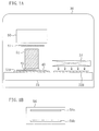
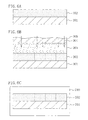
- FIGS. 8A through 8D a conventional pattern formation method employing the immersion lithography will be described with reference to FIGS. 8A through 8D.
- a positive chemically amplified resist material having the following composition is prepared: Base polymer: poly((norbornene-5-methylene-t-butylcarboxylate) (50 mol%) - (maleic anhydride) (50 mol%)) 2 g Acid generator: triphenylsulfonium triflate 0.06 g Quencher: triethanolamine 0.002 g Solvent: propylene glycol monomethyl ether acetate 20 g
- the aforementioned chemically amplified resist material is applied on a substrate 1 so as to form a resist film 2 with a thickness of 0.35 ⁇ m.
- pattern exposure is carried out by irradiating the resist film 2 with exposing light 4 of ArF excimer laser with NA of 0.68 through a mask 5.
- the resist film 2 is baked with a hot plate at a temperature of 110°C for 60 seconds, and the resultant resist film is developed with a 0.26 N tetramethylammonium hydroxide developer. In this manner, a resist pattern 2a made of an unexposed portion of the resist film 2 is formed as shown in FIG. 8D.
- the resist pattern 2a formed by the conventional pattern formation method is in a defective shape.
- the present inventors have variously examined the reason why the resist pattern 2a formed by the conventional immersion lithography is in a defective shape, resulting in finding the following:
- the conventional pattern is in a defective shape because the water 3 used for immersion lithography, which has been discharged from above the resist film 2 after the exposure, still remains on the resist film 2 after the exposure, and remaining drops of the water 3 deteriorate the resist. This deterioration of the resist is caused through contact between the remaining drops and the resist, and the influence of the remaining drops increases with time. Also, it has been found that if the resist film 2 is subjected to the post exposure bake with the drops remaining thereon, the resist is more largely deteriorated.
- the resist is deteriorated by the drops as follows:
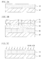
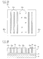
- FIG. 9A schematically shows an example of a plan structure of an exposed resist pattern composed of line patterns 20a and hole patterns 20b and formed on a substrate 10 with an insulating film 15 sandwiched therebetween.
- FIG. 9B is a schematic cross-sectional view taken on line IXb-IXb of FIG. 9A. As shown in FIG.
- the chemical state of the surface of the exposed resist film 20 is largely different from that attained before the exposure, and the line patterns 20a and the hole patterns 20b corresponding to exposed portions where an acid is generated through the exposure and an unexposed portion 20c (where no acid is generated) are present in a mixed manner in accordance with the layout of mask patterns.
- a portion where the largest amount of acid has been generated on the resist film 20 is the surface of the exposed portions 20a and 20b of the resist film 20, and the acid in an amount necessary and sufficient for development is not always generated in the whole exposed portions immediately after the exposure. Accordingly, if a small amount of liquid remains on the surface of the resist film 20 immediately after the exposure, the acid elutes from the surfaces of the exposed portions 20a and 20b, where the largest amount of acid is present, into a remaining drop 30 of the liquid as shown in FIG. 9B. Furthermore, the drop 30 spreads between and partially covers adjacent exposed portions 20a as shown in FIG.
- the pattern is formed in a defective shape because part of the exposed portions 20a and 20b does not dissolve in the development or part of the unexposed portion 20c dissolves in the developer.
- the pattern is refined in such a manner that, for example, the distance between the line patterns 20a is 0.25 ⁇ m or less or the size of the hole pattern is 0.30 ⁇ m or less, even a small amount of liquid spreads over adjacent line patterns 20a. Furthermore, even when a small amount of acid is eluted owing to the drops, the solubility in the developer is largely lowered if the pattern size is smaller.
- the resultant pattern of the target film is also in a defective shape, and hence, the productivity and the yield of the fabrication process for semiconductor devices are disadvantageously lowered.
- an object of the invention is forming a fine pattern in a good shape by preventing a resist film from being deteriorated by drops of a liquid having been used for immersion lithography.
- an immersion liquid is discharged after pattern exposure, and remaining drops of the immersion liquid are removed and dried so that none of the immersion liquid can remain on a resist film.
- the exposure system of this invention includes an exposure section for irradiating a formed resist film with exposing light through a mask with an immersion liquid provided on the resist film; and a drying section for drying a surface of the resist film after irradiation.
- the resist film can be prevented from being deteriorated by remaining drops of the liquid. Accordingly, when the resist film is developed in a development system thereafter, degradation of a pattern shape derived from insufficient dissolution in a developer or unwanted dissolution of an insoluble portion can be prevented in an exposed portion or an unexposed portion of the exposed resist film, resulting in obtaining a resist pattern in a good shape.
- the drying section preferably includes air blowing means.
- the drying section preferably includes dehumidification means.
- the drying section preferably includes warming means.
- the resist film is preferably formed on a wafer, and the drying section preferably dries a whole top surface of the wafer.
- the exposure section preferably includes twin stages having at least two wafer placing portions, and the whole top surface of the wafer is preferably dried on one of the wafer placing portions of the twin stages.
- the air blowing means is preferably an air fan capable of blowing warm air.
- the dehumidification means can be a dehumidification apparatus for lowering humidity of an environment around the resist film by using a refrigerant.
- the refrigerant can be a hydrocarbon-based gas such as isobutane, butane, propane or cyclopropane, and the refrigerant is circulated through a compressor.
- the dehumidification means can be a drying agent for lowering humidity of an atmosphere around the resist film.
- An example of the drying agent is desiccant, and such a drying agent adsorbs moisture contained in the atmosphere for dehumidification.
- the warming means can be a warming apparatus for warming an atmosphere around the resist film.
- the first pattern formation method of this invention includes the steps of forming a resist film on a substrate; performing pattern exposure by selectively irradiating the resist film with exposing light with an immersion liquid provided on the resist film; removing the immersion liquid remaining on a surface of the resist film after the pattern exposure; and forming a resist pattern by developing the resist film after removing the immersion liquid.
- the resist film can be prevented from being deteriorated by the remaining drops of the immersion liquid. Therefore, degradation of the pattern shape derived from insufficient dissolution in a developer or unwanted dissolution of an insoluble portion can be prevented in an exposed portion or an unexposed portion of the resist film, resulting in obtaining the resist pattern in a good shape.
- the step of removing the immersion liquid is preferably a step of blowing air against the resist film after the pattern exposure, a step of dehumidifying an atmosphere around the resist film after the pattern exposure, or a step of warming the resist film after the pattern exposure.
- the second pattern formation method of this invention includes the steps of forming a resist film on a substrate; performing pattern exposure by selectively irradiating the resist film with exposing light with an immersion liquid provided on the resist film; blowing air against the resist film after the pattern exposure; and forming a resist pattern by developing the resist film after blowing air against the resist film.
- the resist film can be prevented from being deteriorated by the drops. Accordingly, degradation of the pattern shape derived from insufficient dissolution in a developer or unwanted dissolution of an insoluble portion can be prevented in an exposed portion or an unexposed portion of the resist film, resulting in obtaining the resist pattern in a good shape.
- the third pattern formation method of this invention includes the steps of forming a resist film on a substrate; performing pattern exposure by selectively irradiating the resist film with exposing light with an immersion liquid provided on the resist film; dehumidifying an atmosphere around the resist film after the pattern exposure; and forming a resist pattern by developing the resist film after dehumidification.
- the drops are evaporated by dehumidifying the atmosphere around the resist film and the surface of the resist film is dried, and therefore, the resist film can be prevented from being deteriorated by the drops. Accordingly, degradation of the pattern shape derived from insufficient dissolution in a developer or unwanted dissolution of an insoluble portion can be prevented in an exposed portion or an unexposed portion of the resist film, resulting in obtaining the resist pattern in a good shape.
- the fourth pattern formation method of this invention includes the steps of forming a resist film on a substrate; performing pattern exposure by selectively irradiating the resist film with exposing light with an immersion liquid provided on the resist film; warming the resist film after the pattern exposure; and forming a resist pattern by developing the resist film after warming the resist film.
- the resist film can be prevented from being deteriorated by the drops. Accordingly, degradation of the pattern shape derived from insufficient dissolution in a developer or unwanted dissolution of an insoluble portion can be prevented in an exposed portion or an unexposed portion of the resist film, resulting in obtaining the resist pattern in a good shape.
- the air is preferably warm air.
- the atmosphere is dehumidified preferably by using a refrigerant.
- the atmosphere is dehumidified preferably by using a drying agent.
- the immersion liquid can be water or perfluoropolyether.
- the exposing light can be KrF excimer laser, Xe 2 laser, ArF excimer laser, F 2 laser, KrAr laser
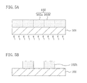
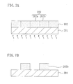
- FIG. 1A schematically shows the cross-sectional structure of a principal part of an exposure system used for realizing a pattern formation method employing immersion lithography according to Embodiment 1 of the invention and FIG. 1B schematically shows the plan structure of an air fan provided in the exposure system.
- the exposure system of Embodiment 1 includes an illumination optical system 50, that is, an exposure section provided within a chamber 30, corresponding to a light source for exposing a design pattern on a resist film (not shown) applied on a wafer 40; a projection lens 51 provided below the illumination optical system 50 for projecting, through an immersion liquid 42 onto the resist film, exposing light emitted from the illumination optical system 50 and entering through a mask (reticle) 41 having the design pattern to be transferred onto the resist film; and a first wafer stage 52A for holding the wafer 40.
- the projection lens 51 is held so as to be in contact with the surface of the immersion liquid 42 supplied onto the resist film formed on the wafer 40 during exposure.
- the first wafer stage 52A is held on a surface plate 53, and the surface plate 53 has what is called twin stages in which a second wafer stage 52B is provided on the side of the first wafer stage 52A.
- the surface plate 53 may have three or more wafer stages.
- an air fan 54 corresponding to a drying section capable of blowing warm air is provided above the second wafer stage 52B of the surface plate 53.
- FIG. 1B is a plan view of the air fan 54.
- a draft port 54a in the shape of a slit penetrating the air fan 54 in the vertical direction and an exhaust port 54b extending in parallel to the draft port 54a are provided on the top face of the air fan 54.
- the exhaust port 54b is communicated with another exhaust port for discharging the air to the outside of the chamber 30.
- the air fan 54 it is not always necessary to provide the air fan 54 above the second wafer stage 52B but it may be provided on the side of the second wafer stage 52B (the surface plate 53) so that the air can blow from the side of the wafer 40 along a direction substantially parallel to the principal surface. Alternatively, it is not always necessary to provide the air fan 54 within the chamber 30 but it may be provided outside the chamber 30.
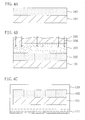
- FIGS. 1A and 1B Now, a pattern formation method using the exposure system of FIGS. 1A and 1B will be described with reference to FIGS. 2A through 2C, 3A and 3B.
- a positive chemically amplified resist material having the following composition is prepared: Base polymer: poly((norbornene-5-methylene-t-butylcarboxylate) (50 mol%) - (maleic anhydride) (50 mol%)) 2 g Acid generator: triphenylsulfonium triflate 0.06 g Quencher: triethanolamine 0.002 g Solvent: propylene glycol monomethyl ether acetate 20 g
- the aforementioned chemically amplified resist material is applied on a wafer 40 so as to form a resist film 43 with a thickness of 0.35 ⁇ m.
- pattern exposure is carried out by irradiating the resist film 43 through a mask (not shown) with exposing light 44 of ArF excimer laser with NA of 0.68.
- the wafer 40 After discharging the liquid 42 from above the resist film 43, the wafer 40 is moved to be positioned below the air fan 54 of FIG. 1A. Thereafter, the top face of the resist film 43 is exposed to the warm air of a temperature of approximately 35°C as shown in FIG. 2C, thereby drying drops of the liquid remaining on the top face of the exposed resist film 43.
- the resist film 43 whose surface has been dried after the exposure, is baked with a hot plate at a temperature of 105°C for 60 seconds, and thereafter, the resultant resist film 102 is developed with a 0.26 N tetramethylammonium hydroxide aqueous solution (alkaline developer). In this manner, a resist pattern 43b made of an unexposed portion of the resist film 43 and having a line width of 0.09 ⁇ m is formed as shown in FIG. 3B.
- the resist film 43 can be prevented from being deteriorated by the drops after the exposure. Accordingly, degradation of the pattern shape derived from insufficient dissolution in the developer of an exposed portion 43a of the resist film 43 or unwanted dissolution of the unexposed portion can be prevented, resulting in obtaining the resist pattern 43b in a good shape.
- the temperature of the warm air blown by the air fan 54 is preferably, for example, not less than room temperature (23°C) and not more than 60°C, which does not limit the invention.
- Embodiment 2 of the invention will be described with reference to FIGS. 4A through 4C, 5A and 5B.
- a positive chemically amplified resist material having the following composition is prepared: Base polymer: poly((norbornene-5-methylene-t-butylcarboxylate) (50 mol%) - (maleic anhydride) (50 mol%)) 2 g Acid generator: triphenylsulfonium triflate 0.06 g Quencher: triethanolamine 0.002 g Solvent: propylene glycol monomethyl ether acetate 20 g
- the aforementioned chemically amplified resist material is applied on a wafer (substrate) 101 so as to form a resist film 102 with a thickness of 0.35 ⁇ m.
- pattern exposure is carried out by irradiating the resist film 102 through a mask (not shown) with exposing light 104 of ArF excimer laser with NA of 0.68.
- the wafer 101 is moved to be placed in a dehumidification vessel 110 provided with a drying agent 111 such as desiccant.
- a drying agent 111 such as desiccant.
- the inside atmosphere of the dehumidification vessel 110 is dehumidified by the drying agent 111 contained therein, and therefore, drops of the liquid remaining on the top face of the exposed resist film 102 are dried.
- the resist film 102 whose surface has been dried after the exposure, is baked with a hot plate at a temperature of 105°C for 60 seconds, and thereafter, the resultant resist film 102 is developed with a 0.26 N tetramethylammonium hydroxide aqueous solution (alkaline developer). In this manner, a resist pattern 102b made of an unexposed portion of the resist film 102 and having a line width of 0.09 ⁇ m is formed as shown in FIG. 5B.
- the resist film 102 can be prevented from being deteriorated by the drops after the exposure. Accordingly, degradation of the pattern shape derived from insufficient dissolution in the developer of an exposed portion 102a of the resist film 102 or unwanted dissolution of the unexposed portion can be prevented, resulting in obtaining the resist pattern 102b in a good shape.
- the drying agent 111 is not limited to the desiccant. Also, the dehumidification means is not limited to the drying agent 111, but for example, a compressor system in which moisture vapor within an atmosphere is set by using a cooler containing a refrigerant may be used for the dehumidification.
- Embodiment 3 of the invention will be described with reference to FIGS. 6A through 6C, 7A and 7B.
- a positive chemically amplified resist material having the following composition is prepared: Base polymer: poly((norbornene-5-methylene-t-butylcarboxylate) (50 mol%) - (maleic anhydride) (50 mol%)) 2 g Acid generator: triphenylsulfonium triflate 0.06 g Quencher: triethanolamine 0.002 g Solvent: propylene glycol monomethyl ether acetate 20 g
- the aforementioned chemically amplified resist material is applied on a wafer (substrate) 201 so as to form a resist film 202 with a thickness of 0.35 ⁇ m.
- pattern exposure is carried out by irradiating the resist film 202 through a mask (not shown) with exposing light 204 of ArF excimer laser with NA of 0.68.
- the wafer 201 is moved to be positioned in a warming vessel 210 in which the atmosphere is warmed to approximately 33°C.
- a warming vessel 210 in which the atmosphere is warmed to approximately 33°C.
- the resist film 202 whose surface has been dried after the exposure, is baked with a hot plate at a temperature of 105°C for 60 seconds, and thereafter, the resultant resist film 202 is developed with a 0.26 N tetramethylammonium hydroxide aqueous solution (alkaline developer). In this manner, a resist pattern 202b made of an unexposed portion of the resist film 202 and having a line width of 0.09 ⁇ m is formed as shown in FIG. 7B.
- the resist film 202 can be prevented from being deteriorated by the drops after the exposure. Accordingly, degradation of the pattern shape derived from insufficient dissolution in the developer of an exposed portion 202a of the resist film 202 or unwanted dissolution of the unexposed portion can be prevented, resulting in obtaining the resist pattern 202b in a good shape.
- the means for warming the exposed resist film 202 for example, a heater provided within the warming vessel 210 may be used.
- the warming vessel 210 for warming the wafer 201 is not always necessary as far as the temperature of the atmosphere covering the resist film 202 can be, for example, not less than room temperature (23°C) and not more than 60°C, which does not limit the invention.
- Embodiments 1 through 3 Although a positive resist is used in each of Embodiments 1 through 3, the present invention is applicable to a negative resist.
- perfluoropolyether may be used instead of water.
- a surfactant may be added to the immersion liquid.
- ArF excimer laser is used as the exposing light for the pattern exposure in each embodiment, KrF excimer laser, Xe 2 laser, F 2 laser, KrAr laser, Ar 2 laser or the like may be used instead.
- a resist can be prevented from being deteriorated by an immersion liquid remaining on the resist, and hence, a resist pattern can be formed in a good shape.
- the invention is useful as, for example, an exposure system and a pattern formation method using the same for use in fabrication process or the like for semiconductor devices.
Landscapes
- General Physics & Mathematics (AREA)
- Physics & Mathematics (AREA)
- Health & Medical Sciences (AREA)
- Toxicology (AREA)
- Engineering & Computer Science (AREA)
- Environmental & Geological Engineering (AREA)
- Epidemiology (AREA)
- Public Health (AREA)
- Atmospheric Sciences (AREA)
- Life Sciences & Earth Sciences (AREA)
- Exposure Of Semiconductors, Excluding Electron Or Ion Beam Exposure (AREA)
- Exposure And Positioning Against Photoresist Photosensitive Materials (AREA)
- Photosensitive Polymer And Photoresist Processing (AREA)
Applications Claiming Priority (1)
| Application Number | Priority Date | Filing Date | Title |
|---|---|---|---|
| JP2004259769A JP2006080143A (ja) | 2004-09-07 | 2004-09-07 | 露光装置及びパターン形成方法 |
Publications (2)
| Publication Number | Publication Date |
|---|---|
| EP1632813A2 true EP1632813A2 (fr) | 2006-03-08 |
| EP1632813A3 EP1632813A3 (fr) | 2007-10-24 |
Family
ID=34981993
Family Applications (1)
| Application Number | Title | Priority Date | Filing Date |
|---|---|---|---|
| EP05018106A Withdrawn EP1632813A3 (fr) | 2004-09-07 | 2005-08-19 | Système d'exposition et procédé pour la formation de motifs |
Country Status (4)
| Country | Link |
|---|---|
| US (2) | US7470501B2 (fr) |
| EP (1) | EP1632813A3 (fr) |
| JP (1) | JP2006080143A (fr) |
| CN (1) | CN1746774A (fr) |
Cited By (2)
| Publication number | Priority date | Publication date | Assignee | Title |
|---|---|---|---|---|
| US8780321B2 (en) | 2008-12-08 | 2014-07-15 | Asml Netherlands B.V. | Lithographic apparatus and device manufacturing method |
| US9013673B2 (en) | 2009-12-02 | 2015-04-21 | Asml Netherlands B.V. | Lithographic apparatus and device manufacturing method |
Families Citing this family (8)
| Publication number | Priority date | Publication date | Assignee | Title |
|---|---|---|---|---|
| KR101037057B1 (ko) * | 2002-12-10 | 2011-05-26 | 가부시키가이샤 니콘 | 노광 장치 및 디바이스 제조 방법 |
| US20070242248A1 (en) * | 2004-10-26 | 2007-10-18 | Nikon Corporation | Substrate processing method, exposure apparatus, and method for producing device |
| US8040489B2 (en) * | 2004-10-26 | 2011-10-18 | Nikon Corporation | Substrate processing method, exposure apparatus, and method for producing device by immersing substrate in second liquid before immersion exposure through first liquid |
| JP2006220847A (ja) * | 2005-02-09 | 2006-08-24 | Toshiba Corp | レジストパターン形成方法 |
| JP2010128464A (ja) * | 2008-12-01 | 2010-06-10 | Az Electronic Materials Kk | レジストパターン形成方法 |
| JP4853536B2 (ja) * | 2009-03-13 | 2012-01-11 | 東京エレクトロン株式会社 | 塗布、現像装置、塗布、現像方法及び記憶媒体 |
| NL2005717A (en) * | 2009-12-18 | 2011-06-21 | Asml Netherlands Bv | A lithographic apparatus and a device manufacturing method. |
| KR101941596B1 (ko) | 2014-06-16 | 2019-01-23 | 에이에스엠엘 네델란즈 비.브이. | 리소그래피 장치, 기판을 이송하는 방법 및 디바이스 제조 방법 |
Citations (5)
| Publication number | Priority date | Publication date | Assignee | Title |
|---|---|---|---|---|
| EP0605103A1 (fr) | 1992-11-27 | 1994-07-06 | Canon Kabushiki Kaisha | Dispositif de projection pour l'exposition immergée |
| WO2005024325A2 (fr) | 2003-08-29 | 2005-03-17 | Tokyo Electron Limited | Procede et systeme de sechage d'un substrat |
| EP1598705A1 (fr) | 2004-05-18 | 2005-11-23 | ASML Netherlands B.V. | Appareil lithographique et méthode de fabrication d'un dispositif |
| EP1601008A1 (fr) | 2003-03-04 | 2005-11-30 | Tokyo Ohka Kogyo Co., Ltd. | Liquide d'immersion pour procede d'exposition par immersion et procede de formation de motif de reserve au moyen d'un tel liquide d'immersion |
| EP1672682A1 (fr) | 2003-10-08 | 2006-06-21 | Zao Nikon Co., Ltd. | Appareil et procede de transport de substrat, appareil et procede d'exposition, et procede de production de dispositif |
Family Cites Families (6)
| Publication number | Priority date | Publication date | Assignee | Title |
|---|---|---|---|---|
| TWI300790B (en) * | 2001-02-28 | 2008-09-11 | Shinetsu Chemical Co | Polymers, Resist Compositions and Patterning Process |
| JP2004002324A (ja) | 2002-03-22 | 2004-01-08 | Kumiai Chem Ind Co Ltd | 除草剤組成物 |
| JP3977324B2 (ja) * | 2002-11-12 | 2007-09-19 | エーエスエムエル ネザーランズ ビー.ブイ. | リソグラフィ装置 |
| CN100440431C (zh) | 2003-03-04 | 2008-12-03 | 东京応化工业株式会社 | 液浸曝光工艺用浸渍液及使用该浸渍液的抗蚀剂图案形成方法 |
| US7169530B2 (en) * | 2003-10-02 | 2007-01-30 | Matsushita Electric Industrial Co., Ltd. | Polymer compound, resist material and pattern formation method |
| JP4194495B2 (ja) | 2004-01-07 | 2008-12-10 | 東京エレクトロン株式会社 | 塗布・現像装置 |
-
2004
- 2004-09-07 JP JP2004259769A patent/JP2006080143A/ja active Pending
-
2005
- 2005-08-15 US US11/203,161 patent/US7470501B2/en active Active
- 2005-08-19 EP EP05018106A patent/EP1632813A3/fr not_active Withdrawn
- 2005-09-07 CN CNA2005100991842A patent/CN1746774A/zh active Pending
-
2008
- 2008-12-05 US US12/314,208 patent/US20090091719A1/en not_active Abandoned
Patent Citations (5)
| Publication number | Priority date | Publication date | Assignee | Title |
|---|---|---|---|---|
| EP0605103A1 (fr) | 1992-11-27 | 1994-07-06 | Canon Kabushiki Kaisha | Dispositif de projection pour l'exposition immergée |
| EP1601008A1 (fr) | 2003-03-04 | 2005-11-30 | Tokyo Ohka Kogyo Co., Ltd. | Liquide d'immersion pour procede d'exposition par immersion et procede de formation de motif de reserve au moyen d'un tel liquide d'immersion |
| WO2005024325A2 (fr) | 2003-08-29 | 2005-03-17 | Tokyo Electron Limited | Procede et systeme de sechage d'un substrat |
| EP1672682A1 (fr) | 2003-10-08 | 2006-06-21 | Zao Nikon Co., Ltd. | Appareil et procede de transport de substrat, appareil et procede d'exposition, et procede de production de dispositif |
| EP1598705A1 (fr) | 2004-05-18 | 2005-11-23 | ASML Netherlands B.V. | Appareil lithographique et méthode de fabrication d'un dispositif |
Non-Patent Citations (1)
| Title |
|---|
| M. SWITKES; M. ROTHSCHILD: "Immersion lithography at 157 nm", J. VAC. SCI. TECHNOL., vol. B19, 2001, pages 2353 |
Cited By (2)
| Publication number | Priority date | Publication date | Assignee | Title |
|---|---|---|---|---|
| US8780321B2 (en) | 2008-12-08 | 2014-07-15 | Asml Netherlands B.V. | Lithographic apparatus and device manufacturing method |
| US9013673B2 (en) | 2009-12-02 | 2015-04-21 | Asml Netherlands B.V. | Lithographic apparatus and device manufacturing method |
Also Published As
| Publication number | Publication date |
|---|---|
| US20090091719A1 (en) | 2009-04-09 |
| JP2006080143A (ja) | 2006-03-23 |
| US20060051709A1 (en) | 2006-03-09 |
| CN1746774A (zh) | 2006-03-15 |
| EP1632813A3 (fr) | 2007-10-24 |
| US7470501B2 (en) | 2008-12-30 |
Similar Documents
| Publication | Publication Date | Title |
|---|---|---|
| US20090091719A1 (en) | Exposure system and pattern formation method | |
| US7094521B2 (en) | Pattern formation method and exposure system | |
| US7524772B2 (en) | Pattern formation method | |
| US8088565B2 (en) | Exposure system and pattern formation method | |
| US7393794B2 (en) | Pattern formation method | |
| US7541132B2 (en) | Chemically amplified resist material, topcoat film material and pattern formation method using the same | |
| US7700268B2 (en) | Exposure system and pattern formation method using the same | |
| US9847226B2 (en) | Manufacturing method of semiconductor device | |
| US20080032239A1 (en) | Pattern formation method | |
| US6902999B2 (en) | Pattern formation method | |
| US7595142B2 (en) | Pattern formation method | |
| US20070111541A1 (en) | Barrier film material and pattern formation method using the same | |
| EP1610180A2 (fr) | Appareil de fabrication de semi-conducteurs et procédé de formation de motifs | |
| EP1600815A2 (fr) | Appareil de fabrication de semiconducteurs et méthode pour réaliser des motifs | |
| US20040009433A1 (en) | Pattern formation method | |
| US20050164122A1 (en) | Chemically amplified resist and pattern formation method | |
| JP2003142390A (ja) | レジスト処理方法および半導体装置の製造方法 | |
| US20040058271A1 (en) | Pattern formation material, water-soluble material and pattern formation method | |
| JP3696185B2 (ja) | 露光装置及びパターン形成方法 | |
| US20060194449A1 (en) | Resist pattern forming method and method of manufacturing semiconductor device |
Legal Events
| Date | Code | Title | Description |
|---|---|---|---|
| PUAI | Public reference made under article 153(3) epc to a published international application that has entered the european phase |
Free format text: ORIGINAL CODE: 0009012 |
|
| AK | Designated contracting states |
Kind code of ref document: A2 Designated state(s): AT BE BG CH CY CZ DE DK EE ES FI FR GB GR HU IE IS IT LI LT LU LV MC NL PL PT RO SE SI SK TR |
|
| AX | Request for extension of the european patent |
Extension state: AL BA HR MK YU |
|
| PUAL | Search report despatched |
Free format text: ORIGINAL CODE: 0009013 |
|
| AK | Designated contracting states |
Kind code of ref document: A3 Designated state(s): AT BE BG CH CY CZ DE DK EE ES FI FR GB GR HU IE IS IT LI LT LU LV MC NL PL PT RO SE SI SK TR |
|
| AX | Request for extension of the european patent |
Extension state: AL BA HR MK YU |
|
| 17P | Request for examination filed |
Effective date: 20080421 |
|
| AKX | Designation fees paid |
Designated state(s): DE FR NL |
|
| RAP1 | Party data changed (applicant data changed or rights of an application transferred) |
Owner name: PANASONIC CORPORATION |
|
| STAA | Information on the status of an ep patent application or granted ep patent |
Free format text: STATUS: THE APPLICATION HAS BEEN WITHDRAWN |
|
| 18W | Application withdrawn |
Effective date: 20090810 |