EP1489654A1 - LnCuO(S, Se, Te) MONOCRYSTALLINE THIN FILM, ITS MANUFACTURING METHOD, AND OPTICAL DEVICE OR ELECTRONIC DEVICE USING THE MONOCRYSTALLINE THIN FILM - Google Patents
LnCuO(S, Se, Te) MONOCRYSTALLINE THIN FILM, ITS MANUFACTURING METHOD, AND OPTICAL DEVICE OR ELECTRONIC DEVICE USING THE MONOCRYSTALLINE THIN FILM Download PDFInfo
- Publication number
- EP1489654A1 EP1489654A1 EP03705304A EP03705304A EP1489654A1 EP 1489654 A1 EP1489654 A1 EP 1489654A1 EP 03705304 A EP03705304 A EP 03705304A EP 03705304 A EP03705304 A EP 03705304A EP 1489654 A1 EP1489654 A1 EP 1489654A1
- Authority
- EP
- European Patent Office
- Prior art keywords
- thin film
- lncuox
- crystal
- film
- lacuos
- Prior art date
- Legal status (The legal status is an assumption and is not a legal conclusion. Google has not performed a legal analysis and makes no representation as to the accuracy of the status listed.)
- Granted
Links
Images




Classifications
-
- C—CHEMISTRY; METALLURGY
- C30—CRYSTAL GROWTH
- C30B—SINGLE-CRYSTAL GROWTH; UNIDIRECTIONAL SOLIDIFICATION OF EUTECTIC MATERIAL OR UNIDIRECTIONAL DEMIXING OF EUTECTOID MATERIAL; REFINING BY ZONE-MELTING OF MATERIAL; PRODUCTION OF A HOMOGENEOUS POLYCRYSTALLINE MATERIAL WITH DEFINED STRUCTURE; SINGLE CRYSTALS OR HOMOGENEOUS POLYCRYSTALLINE MATERIAL WITH DEFINED STRUCTURE; AFTER-TREATMENT OF SINGLE CRYSTALS OR A HOMOGENEOUS POLYCRYSTALLINE MATERIAL WITH DEFINED STRUCTURE; APPARATUS THEREFOR
- C30B33/00—After-treatment of single crystals or homogeneous polycrystalline material with defined structure
-
- C—CHEMISTRY; METALLURGY
- C30—CRYSTAL GROWTH
- C30B—SINGLE-CRYSTAL GROWTH; UNIDIRECTIONAL SOLIDIFICATION OF EUTECTIC MATERIAL OR UNIDIRECTIONAL DEMIXING OF EUTECTOID MATERIAL; REFINING BY ZONE-MELTING OF MATERIAL; PRODUCTION OF A HOMOGENEOUS POLYCRYSTALLINE MATERIAL WITH DEFINED STRUCTURE; SINGLE CRYSTALS OR HOMOGENEOUS POLYCRYSTALLINE MATERIAL WITH DEFINED STRUCTURE; AFTER-TREATMENT OF SINGLE CRYSTALS OR A HOMOGENEOUS POLYCRYSTALLINE MATERIAL WITH DEFINED STRUCTURE; APPARATUS THEREFOR
- C30B1/00—Single-crystal growth directly from the solid state
- C30B1/02—Single-crystal growth directly from the solid state by thermal treatment, e.g. strain annealing
-
- C—CHEMISTRY; METALLURGY
- C30—CRYSTAL GROWTH
- C30B—SINGLE-CRYSTAL GROWTH; UNIDIRECTIONAL SOLIDIFICATION OF EUTECTIC MATERIAL OR UNIDIRECTIONAL DEMIXING OF EUTECTOID MATERIAL; REFINING BY ZONE-MELTING OF MATERIAL; PRODUCTION OF A HOMOGENEOUS POLYCRYSTALLINE MATERIAL WITH DEFINED STRUCTURE; SINGLE CRYSTALS OR HOMOGENEOUS POLYCRYSTALLINE MATERIAL WITH DEFINED STRUCTURE; AFTER-TREATMENT OF SINGLE CRYSTALS OR A HOMOGENEOUS POLYCRYSTALLINE MATERIAL WITH DEFINED STRUCTURE; APPARATUS THEREFOR
- C30B23/00—Single-crystal growth by condensing evaporated or sublimed materials
- C30B23/02—Epitaxial-layer growth
-
- C—CHEMISTRY; METALLURGY
- C30—CRYSTAL GROWTH
- C30B—SINGLE-CRYSTAL GROWTH; UNIDIRECTIONAL SOLIDIFICATION OF EUTECTIC MATERIAL OR UNIDIRECTIONAL DEMIXING OF EUTECTOID MATERIAL; REFINING BY ZONE-MELTING OF MATERIAL; PRODUCTION OF A HOMOGENEOUS POLYCRYSTALLINE MATERIAL WITH DEFINED STRUCTURE; SINGLE CRYSTALS OR HOMOGENEOUS POLYCRYSTALLINE MATERIAL WITH DEFINED STRUCTURE; AFTER-TREATMENT OF SINGLE CRYSTALS OR A HOMOGENEOUS POLYCRYSTALLINE MATERIAL WITH DEFINED STRUCTURE; APPARATUS THEREFOR
- C30B29/00—Single crystals or homogeneous polycrystalline material with defined structure characterised by the material or by their shape
- C30B29/10—Inorganic compounds or compositions
- C30B29/16—Oxides
- C30B29/22—Complex oxides
-
- H—ELECTRICITY
- H10—SEMICONDUCTOR DEVICES; ELECTRIC SOLID-STATE DEVICES NOT OTHERWISE PROVIDED FOR
- H10D—INORGANIC ELECTRIC SEMICONDUCTOR DEVICES
- H10D62/00—Semiconductor bodies, or regions thereof, of devices having potential barriers
- H10D62/80—Semiconductor bodies, or regions thereof, of devices having potential barriers characterised by the materials
-
- H—ELECTRICITY
- H10—SEMICONDUCTOR DEVICES; ELECTRIC SOLID-STATE DEVICES NOT OTHERWISE PROVIDED FOR
- H10P—GENERIC PROCESSES OR APPARATUS FOR THE MANUFACTURE OR TREATMENT OF DEVICES COVERED BY CLASS H10
- H10P14/00—Formation of materials, e.g. in the shape of layers or pillars
- H10P14/20—Formation of materials, e.g. in the shape of layers or pillars of semiconductor materials
- H10P14/22—Formation of materials, e.g. in the shape of layers or pillars of semiconductor materials using physical deposition, e.g. vacuum deposition or sputtering
-
- H—ELECTRICITY
- H10—SEMICONDUCTOR DEVICES; ELECTRIC SOLID-STATE DEVICES NOT OTHERWISE PROVIDED FOR
- H10P—GENERIC PROCESSES OR APPARATUS FOR THE MANUFACTURE OR TREATMENT OF DEVICES COVERED BY CLASS H10
- H10P14/00—Formation of materials, e.g. in the shape of layers or pillars
- H10P14/20—Formation of materials, e.g. in the shape of layers or pillars of semiconductor materials
- H10P14/29—Formation of materials, e.g. in the shape of layers or pillars of semiconductor materials characterised by the substrates
- H10P14/2901—Materials
- H10P14/2921—Materials being crystalline insulating materials
-
- H—ELECTRICITY
- H10—SEMICONDUCTOR DEVICES; ELECTRIC SOLID-STATE DEVICES NOT OTHERWISE PROVIDED FOR
- H10P—GENERIC PROCESSES OR APPARATUS FOR THE MANUFACTURE OR TREATMENT OF DEVICES COVERED BY CLASS H10
- H10P14/00—Formation of materials, e.g. in the shape of layers or pillars
- H10P14/20—Formation of materials, e.g. in the shape of layers or pillars of semiconductor materials
- H10P14/32—Formation of materials, e.g. in the shape of layers or pillars of semiconductor materials characterised by intermediate layers between substrates and deposited layers
- H10P14/3202—Materials thereof
-
- H—ELECTRICITY
- H10—SEMICONDUCTOR DEVICES; ELECTRIC SOLID-STATE DEVICES NOT OTHERWISE PROVIDED FOR
- H10P—GENERIC PROCESSES OR APPARATUS FOR THE MANUFACTURE OR TREATMENT OF DEVICES COVERED BY CLASS H10
- H10P14/00—Formation of materials, e.g. in the shape of layers or pillars
- H10P14/20—Formation of materials, e.g. in the shape of layers or pillars of semiconductor materials
- H10P14/32—Formation of materials, e.g. in the shape of layers or pillars of semiconductor materials characterised by intermediate layers between substrates and deposited layers
- H10P14/3202—Materials thereof
- H10P14/3234—Materials thereof being oxide semiconducting materials
-
- H—ELECTRICITY
- H10—SEMICONDUCTOR DEVICES; ELECTRIC SOLID-STATE DEVICES NOT OTHERWISE PROVIDED FOR
- H10P—GENERIC PROCESSES OR APPARATUS FOR THE MANUFACTURE OR TREATMENT OF DEVICES COVERED BY CLASS H10
- H10P14/00—Formation of materials, e.g. in the shape of layers or pillars
- H10P14/20—Formation of materials, e.g. in the shape of layers or pillars of semiconductor materials
- H10P14/32—Formation of materials, e.g. in the shape of layers or pillars of semiconductor materials characterised by intermediate layers between substrates and deposited layers
- H10P14/3202—Materials thereof
- H10P14/3236—Materials thereof being chalcogenide semiconducting materials not being oxides, e.g. ternary compounds
-
- H—ELECTRICITY
- H10—SEMICONDUCTOR DEVICES; ELECTRIC SOLID-STATE DEVICES NOT OTHERWISE PROVIDED FOR
- H10P—GENERIC PROCESSES OR APPARATUS FOR THE MANUFACTURE OR TREATMENT OF DEVICES COVERED BY CLASS H10
- H10P14/00—Formation of materials, e.g. in the shape of layers or pillars
- H10P14/20—Formation of materials, e.g. in the shape of layers or pillars of semiconductor materials
- H10P14/32—Formation of materials, e.g. in the shape of layers or pillars of semiconductor materials characterised by intermediate layers between substrates and deposited layers
- H10P14/3202—Materials thereof
- H10P14/3241—Materials thereof being conductive materials
-
- H—ELECTRICITY
- H10—SEMICONDUCTOR DEVICES; ELECTRIC SOLID-STATE DEVICES NOT OTHERWISE PROVIDED FOR
- H10P—GENERIC PROCESSES OR APPARATUS FOR THE MANUFACTURE OR TREATMENT OF DEVICES COVERED BY CLASS H10
- H10P14/00—Formation of materials, e.g. in the shape of layers or pillars
- H10P14/20—Formation of materials, e.g. in the shape of layers or pillars of semiconductor materials
- H10P14/34—Deposited materials, e.g. layers
- H10P14/3402—Deposited materials, e.g. layers characterised by the chemical composition
- H10P14/3434—Deposited materials, e.g. layers characterised by the chemical composition being oxide semiconductor materials
-
- H—ELECTRICITY
- H10—SEMICONDUCTOR DEVICES; ELECTRIC SOLID-STATE DEVICES NOT OTHERWISE PROVIDED FOR
- H10P—GENERIC PROCESSES OR APPARATUS FOR THE MANUFACTURE OR TREATMENT OF DEVICES COVERED BY CLASS H10
- H10P14/00—Formation of materials, e.g. in the shape of layers or pillars
- H10P14/20—Formation of materials, e.g. in the shape of layers or pillars of semiconductor materials
- H10P14/34—Deposited materials, e.g. layers
- H10P14/3402—Deposited materials, e.g. layers characterised by the chemical composition
- H10P14/3436—Deposited materials, e.g. layers characterised by the chemical composition being chalcogenide semiconductor materials not being oxides, e.g. ternary compounds
-
- H—ELECTRICITY
- H10—SEMICONDUCTOR DEVICES; ELECTRIC SOLID-STATE DEVICES NOT OTHERWISE PROVIDED FOR
- H10H—INORGANIC LIGHT-EMITTING SEMICONDUCTOR DEVICES HAVING POTENTIAL BARRIERS
- H10H20/00—Individual inorganic light-emitting semiconductor devices having potential barriers, e.g. light-emitting diodes [LED]
- H10H20/80—Constructional details
- H10H20/81—Bodies
- H10H20/822—Materials of the light-emitting regions
Definitions
- the present invention relates to a method of producing an LnCuO(S, Se, Te) single-crystal thin film (wherein Ln is at least one selected from the group consisting of lanthanide elements and yttrium (Y)), a single-crystal thin film obtained through the production method, and an optical or electronic device using the single-crystal thin film.
- Vapor-phase epitaxial growth means that, when a deposited film is grown on a single-crystal substrate in a vacuum atmosphere, the growth proceeds while maintaining a given relationship between the respective crystal orientations of the substrate and the deposited film under the influence of the orderly atomic arrangement of the crystal of the substrate.
- a typical thin film growth technology based on the epitaxial growth includes a sputtering process, a chemical vapor deposition (CVD) process, a molecular beam epitaxy (MBE) process and a pulsed laser deposition (PLD) process.
- a sputtering process for use as a film forming method utilizes a so-called sputtering-phenomenon discovered by W. Grove in 1852.
- the sputtering phenomenon means that high-kinetic energy particles emitted onto the surface of a target (ions or atoms neutralized by electrons around the target surface) give the kinetic momentum of the particles to constitutive atoms of the target through an elastic collision therebetween, and the recoil atoms are finally released from the target surface after repeatedly colliding with adjacent atoms.
- the film forming method based on the sputtering process is intended to deposit the released constitutive atoms of the target on a substrate so as to form a thin film.
- the chemical vapor deposition (CVD) process is intended to grow a thin film having a desired composition on a substrate by using chloride or organometal compound as a source material, and inducing the chemical reaction between source gases on the substrate.
- the CVD process having excellent compatibility to mass production is widely used to produce practical materials for semiconductor lasers and others.
- the molecular beam epitaxy (MBE) process is a thin-film crystal growth technology named in 1968 by J. R. Arthur who was with Bell Laboratory at the time, and developed for compound semiconductors, primarily GaAs.
- the MBE process can be considered as an improved or progressive type of a vacuum deposition process.
- the MBE process is intended to perform an epitaxial crystal growth under the conditions that the flow of neutral molecules (or atoms) serving as raw materials of a crystal to be grown, or the intensity of a molecular beam (atomic beam), is accurately controlled in ultra-high vacuum, and the neutral molecules (or atoms) are emitted onto an accurately temperature-controlled substrate.
- the MBE process can be applied to a wide range of materials including compound semiconductors, elementary semiconductors such as Si, and various metal or oxide superconductors.
- the difference from the conventional vacuum deposition process is in that (i) the vacuum degree in a growth chamber is set at 10 -7 ⁇ 10 -8 Pa or less, (ii) the crystal growth is performed while stably maintaining the cleanness of the crystal surface at the atomic scale, and (iii) the intensity of the molecular beam is accurately controlled.
- Laser ablation means a process of etching the surface of a solid utilizing a phenomenon that when the intensity of laser light emitted onto a solid is increased up to a given threshold value or more, the laser light is converted into electronic, thermal, photochemical and mechanical energies on the solid surface, and consequently various kinds of fragments (neutral atoms, molecules, positive/negative ions, radicals, clusters, etc.) are explosively released from the solid surface.
- the PLD process utilizes the principle of the laser ablation to produce a single-crystal thin film on a substrate under an ultra-high vacuum atmosphere set at a vacuum degree of 10 -7 ⁇ 10 -8 Pa or less in a growth chamber, or under a sufficiently controlled atmosphere based on the flow of reactive gas. While the PLD process is a non-equilibrium process as with the sputtering process, it is different from the sputtering process in that the difference between the respective compositions of a target and an obtained film is small, and single-crystal films of various material can be produced by simply replacing a target. In recent years, the PLD process is actively used, particularly, in the field of research on exploration of substances, by utilizing the above features.
- the present invention is directed to the development of a technique for achieving LnCuOX epitaxial single-crystal thin film growth (wherein Ln is at least one selected from the group consisting of lanthanide elements and yttrium (Y), and X is at least one selected from the group consisting of S, Se and Te) by use of a solid-phase epitaxial process. It has been verified that LnCuOX exhibits luminescence or light-emission originated from excitons even in a polycrystalline film thereof. Therefore, LnCuOX has much promise as materials for light-emitting devices. For example, if an LnCuOX single-crystal thin film is obtained, it can be used as a material of ultraviolet light-emitting devices.
- LnCuOX is a wide-bandgap p-type semiconductor.
- most of wide-bandgap substances such as ZnO and SnO 2 , can not exhibit both n- and p-types conductively but an n-type semiconductor having electrons as a main carrier.
- FET Field Effect Transistor
- a gate operating voltage will be positive.
- LnCuOX which is a wide-bandgap p-type semiconductor
- a gate operating voltage will be negative.
- CMOS Complementary Metal-Oxide Semiconductor
- a wide-bandgap Complementary Metal-Oxide Semiconductor (CMOS) circuit or a high-performance transparent electronic circuit, can be produced by combining this p-type wide-bandgap semiconductor FET with the aforementioned n-type wide-bandgap semiconductor FET.
- the p-type wide-bandgap semiconductor can also be combined with an n-type semiconductor to produce a hetero-junction bipolar transistor or light-emitting diode using a p-n junction.
- LaCuOS layer-structured oxysulfide
- LaCuOS has a layer structure in which a (La 2 O 2 ) 2+ layer and a (Cu 2 S 2 ) 2- layer are alternately stacked along the c-axis of the tetragonal system.
- LaCuOS is a transparent p-type semiconductor having a bandgap of about 3.1 eV which suggests promise as a next-generation wide-bandgap p-type semiconductor material (K. Ueda, S. Inoue, S. Hirose, H. Kawazoe and H. Hosono, Appl. Phys. Lett., 77, 2701 (2000)).
- K. Ueda et al. reported that LaCuOS exhibits exciton-originated optical absorption/emission characteristics having stability even at room temperature, and has promise as a next-generation material of ultraviolet light-emitting devices (K. Ueda, S. Inoue, H. Hosono, N. Sarukura and M. Hirano, Appl. Phys. Lett., 78, 2333 (2001)).
- LnCuOX is increased up to about 10 2 S/cm by substituting the Ln site with divalent alkali earth metal ions of Sr and Ca (K. Ishikawa, S. Kinoshita, Y. Suzuki, S. Matsuura, T. Takanishi, M. Aizawa and Y. Suzuki, J. Electrochem. Soc. 138, 1166 (1991), and Y. Takano, K. Yahagi and K. Sekizawa, Physica A 206&207, 764 (1995)).
- LaCuOS and LaCuOSe prepared by substituting the S site of LaCuOS with Se exhibit complete solid solubility therebetween, and form a solid solution LaCuOS 1-x Se x (0 ⁇ x ⁇ 1) (K. Ueda and H. Hosono, Thin Solid Films, 411, 115 (2002)).
- the bandgap of the LaCuOS 1-x Se x can be controllably changed from 3.1 eV to 2.8 eV by continuously varying the value x representing the amount of substitution from zero to 1 (K. Ueda and H. Hosono, J. Appl. Phys. 91, 4768 (2002)).
- a LaCuOS 1-x Se x film prepared by accurately controlling the value x and the thickness thereof can have a desirably controlled light-emission wavelength. It is also possible to form quantum well structure using the mixed compounds.
- LnCuOX is a wide-bandgap p-type semiconductor and it is expected to be applicable to the active layer of an ultraviolet light-emitting device, it was very difficult to produce a single-crystal thin film thereof.
- a LnCuOX thin film has been produced by annealing an amorphous film at a high temperature which were deposits by a sputtering process under appropriate conditions, (K. Ueda, S. Inoue, S. Hirose, H. Kawazoe and H. Hosono, Appl. Phys. Lett. 77, 2701 (2000)).
- a film produced by the above method was unexceptionally a polycrystalline from incapable of achieving high light-emission efficiency and large electron mobility required for a material of light-emitting devices or electronic devices.
- the present invention provides a method of producing an LnCuOX single-crystal thin film (wherein Ln is at least one selected from the group consisting of lanthanide elements and yttrium, and X is at least one selected from the group consisting of S, Se and Te).
- the method comprises the steps of growing a base thin film on a single-crystal substrate, depositing an amorphous or polycrystalline LnCuOX thin film on the base thin film to form a stacked film, setting the bi-layered film in a vacuum, and then annealing the stacked film at a high temperature of 500°C or more in the vacuum to grow an LnCuOX single-crystal thin film.
- an Ag film an Ag compound film such as an Ag 2 S, Ag 2 O, AgO, AgCl or AgI film, and an Au film
- the components of the base thin film will be entirely left on the single-crystal substrate made of either one of YSZ, Y 2 O 3 , STO, Al 2 O 3 and MgO, or will be partially diffused in LnCuOX and left therein as impurities.
- the stacked film composed of the amorphous or polycrystalline LnCuOX thin film and the base thin film on the single-crystal substrate is annealed while enclosing the film in a vacuum environment, vacuum sealed capsule for example, so as to prevent the components Cu and X from being vaporized during a heating treatment.
- the LnCuOX single-crystal thin film produced in this manner can be used as the active layer of an ultraviolet light-emitting device (diode or laser) by taking advantage of its high light-emission efficiency at room temperature associated with exciton.
- the LnCuOX single-crystal thin film can be used as a channel layer of a field-effect transistor (FET) to produce a transparent FET to be operated at a negative gate voltage.
- FET field-effect transistor
- the FET device combined with n-channel FET to produce a CMOS circuit or a hetero-bipolar device.
- a base thin film may be grown appropriately using a conventional film forming method, such as a sputtering process, a CVD process, a MBE process or a PLD process.
- a single-crystal substrate for use in the method may be made of either one of YSZ, Y 2 O 3 , STO, Al 2 O 3 and MgO.
- a YAS (100), Y 2 O 3 (100) or MgO (100) single crystal is preferably used as the single-crystal substrate, because they have no risk of causing a chemical reaction with an LnCuOX compound even at a high temperature of 1200°C or less.
- the anion-anion nearest-neighbour distance in the substrate crystal plane (A-substrate) is close to the anion-anion nearest-neighbour distance in the C plane of LnCuOX (A-film), or which has less lattice mismatch.
- the A-substrate is 2.82 for LaCuOS, 2.88 for LaCuOSe, 2.96 for MgO(100), 2,58 for YSZ(100), and 2.92 for Y 2 O 3 (100).
- Y 2 O 3 , MgO and YSZ have a higher priority for the single-crystal substrate in this order, in view of the lattice mismatch.
- a base thin film made of either one material selected from the group consisting of Cu, Cu 2 S, CuS, Cu 2 O, CuO, CuCl, CuCl 2 , CuI, Ag, Ag 2 S, Ag 2 O, AgO, AgCl, AgI and Au, is grown on the single-crystal substrate, such as an YSZ, Y 2 O 3 or MgO single-crystal substrate. If the base thin film is made of Cu or Cu-based compound, the components Cu, O and/or S of the base thin film will be mixed in an LnCuOX thin film to be deposited onto the base thin film.
- the base thin film is made of a material other than Cu or Cu-based compound
- the components of the base thin film will be left on the interface between the single-crystal substrate and the LnCuOX thin film, or partially diffused into the LnCuOX thin film.
- an LnCuOX thin film is deposited on the base thin film by using an LnCuOX sintered body as a target, under an H 2 S atmosphere when LnCuOX is LnCuOS, or under an argon or vacuum atmosphere when LnCuOX is LnCuOSe or LnCuOTe. While a sputtering process or a PLD process is preferably used for depositing the LnCuOX thin film in view of their simplicity, the present invention is not limited to such process.
- the LnCuOX thin film to be deposited on the base thin film may be polycrystalline or may be amorphous.
- a solid-solution film may be deposited on the base thin film by using an LnCuOX 1-x X' x (each of X and X' is at least one selected from the group consisting of S, Se and Te, wherein X and X' are different elements; 0 ⁇ x ⁇ 1) solid-solution sintered body as a target.
- LnCuOX 1-x X' x each of X and X' is at least one selected from the group consisting of S, Se and Te, wherein X and X' are different elements; 0 ⁇ x ⁇ 1
- a single-crystal film having the above solid-solution composition is obtained as a final product.
- a stacked of film different in composition may be deposited in the form of multilayer by using two kinds of targets different in Ln or X.
- a solid-solution single-crystal thin film having a composition which is a film-thickness-weighted average of all of the film compositions is obtained as a final
- the solid solution LnCuOX 1-x X' x is useful as a light-emitting material because the light-emission wavelength thereof can be continuously changed by controlling the value of x.
- the forbidden band or energy gap of the solid solution LnCuOX 1-x X' x is continuously changed depending on the value of x.
- artificial superlattice structures is formed by alternately laminating single-crystal films different in the value of x.
- Laminated film composed of the LnCuOX thin film and the base thin film on the single-crystal substrate is enclosed in a vacuum environment, such as in sealed vacuum capsule, and subjected to a heat treatment at a temperature of 500°C or more, preferably 1000°C or more. Under the condition of less than 500°C, any homogeneous single-crystal LnCuOX thin film cannot be obtained due to insufficient diffusion. On the other hand, when a heating temperature is 1200°C or more the undesirable reaction between the single-crystal substrate and the LnCuOX compound takes place. Further, the softening of quartz glass make it unusability as a material to form sealed vacuum capsule.
- the components Cu and X have a high vapor pressure.
- a high-quality LnCuOX single crystal cannot be obtained in some cases, due to significant change in the composition of the thin film obtained after the heat treatment, due to vaporization of the components Cu and X from the LnCuOX thin film.
- the laminated film is enclosed in such a vacuum environment as typically enclosed in a quartz tube which is vacuumized and then hermetically sealed.
- annealing may be carried out in an atmosphere containing LnCuOX vapor, generating in the vacuum sealed chamber LnCuOX vapor having the same chemical formula as that of the single-crystal thin film, compensating the vapor pressure of Cu and X in the vacuum sealed and heated atmosphere. For example, this may be achieved in such a way that LnCuOX powder is enclosed in the closed vacuum environment together with the laminated film.
- the LnCuOX vapor generated during the heating treatment is solidified in the form of particles, and the particles are likely to be deposited on surface of the single-crystal thin film so as to cause the roughened surface thereof.
- the surface of the LnCuOX thin film may be covered by plate, such as YSZ plate, which has no reactivity with the LnCuOX thin film.
- the vaporization of the components Cu and X may also be suppressed by preparing an additional laminated film composed of the LnCuOX thin film and the base thin film on the single-crystal substrate, attaching the respective surfaces of the aforementioned laminated film and the additional laminated film together, and then enclosing these laminated films in the vacuum environment.
- the above additional film may be composed of the LnCuOX thin film on the single-crystal substrate without the base thin film. In this case, only the laminated film having the base thin film will be formed as the LnCuOX single-crystal thin film.
- the Ln site of LnCuOX can be substituted with a divalent ion of a metal M (M is at least one selected from the group consisting of Mg, Ca, Sr, Ba and Zn) to effectively create hole carriers.
- M is at least one selected from the group consisting of Mg, Ca, Sr, Ba and Zn
- the divalent metal ion may be contained in a sintered body target to substitute the Ln site of the LnCuOX thin film with the divalent metal ion.
- the amount of the substitution may be varied to continuously change the electrical conductivity of an Ln 1-y M y CuOX single-crystal thin film (wherein 0 ⁇ y ⁇ 1) from 10 -5 S/cm to 80 S/cm.
- a combination of the single-crystal substrate and the LnCuOX thin film having a large lattice mismatch therebetween is likely to cause difficulties in growing a single-crystal film.
- a LaCuOS 1-x Se x film having x of 0.5 or more is grown on a (100) plane of an YSZ substrate, it is difficult to obtain a single-crystal film.
- a single-crystal LaCuOS 1-x Se x solid-solution thin film can be obtained by growing an LnCuOX single-crystal thin film having less lattice mismatch on a (100) plane of an YSZ substrate through the aforementioned process, depositing an LnCuOSe thin film on the LnCuOX single-crystal thin film to form a laminated film, and annealing the laminated film at a high temperature of 500°C while enclosing the laminated film in a vacuum environment.
- an amorphous or polycrystalline LnCuOX' is solid-phase diffused into the LnCuOX single-crystal thin film to grow an LnCuOX 1-x X' x single-crystal thin film having large lattice mismatch with the single-crystal substrate.
- the Ln site of the LnCuOX single-crystal thin film may be substituted with a divalent ion of the metal M.
- the solid solution LnCuOX 1-x X' x is useful as a material for light emitting devices because the light-emission wavelength thereof can be continuously changed by controlling the value of x.
- the forbidden band or energy gap of the solid solution LnCuOX 1-x X' x is continuously changed depending on the value of x.
- the LnCuOX single-crystal thin film or the Ln 1-y M y CuOX single-crystal thin film obtained in this manner can be laminated to an n-type semiconductor consisting of either one of ZnO, ZnS, In 2 O 3 and SnO 2 to form a PN heterojunction structure so as to produce a light-emitting diode.
- the LnCuOX single-crystal thin film or the Ln 1-y M y CuOX single-crystal thin film can also be combined with ZnO or ZnO : Mg to form a double hetero structure so as to produce a semiconductor laser.
- the LnCuOX single-crystal thin film or the Ln 1-y M y CuOX single-crystal thin film can be used to fabricate a FET by depositing YSZ thereon as a gate insulation film, and depositing Pt-Pd or ITO (Indium-Tin Oxide) thereon as source and drain electrodes.
- the LnCuOX single-crystal thin film or the Ln 1-y M y CuOX single-crystal thin film can be used to fabricate a hetero-bipolar transistor by combining with an n-type semiconductor consisting of either one of ZnO, ZnS, In 2 O 3 and SnO 2 to form a hetero structure, and forming an ohmic electrode on each of the surfaces of the hetero structure.
- Cu thin film was grown on an YSZ (100) single-crystal substrate (10 mm square ⁇ 0.5 mm thickness) through a PLD process at a substrate temperature of 200°C.
- the thickness of the Cu thin film determined by X-ray reflectance and X-ray fluorescence measurements was 5 nm.
- the crystallinity of the grown Cu thin film was evaluated using a HRXRD (High-Resolution X-Ray Diffraction) system. As a result, Cu was oriented toward the (111) plane of the YSZ (100) single-crystal substrate, and the tilt angle was 0.01-degree.
- LaCuOS was deposited on the Cu thin film grown on the YSZ (100) single-crystal substrate as a base layer while maintaining the substrate at room temperature, through a pulsed laser deposition process (PLD process) under an H 2 S atmosphere using a LaCuOS sintered body as a target. Through an X-ray reflectance measurement, it was proved that the thickness of an obtained LaCuOS thin film is 200 nm.
- the deposited LaCuOS thin film was amorphous.
- the laminated films were enclosed in a vacuumized and sealed quartz glass tube together with LaCuOS powder (mean particle size of about 0.1 mm; about 0.1 g). Then, the sealed quartz tube capsule was annealed by heating in an ambient atmosphere at 1000°C for 30 minutes. After the heat treatment, the laminated films were cooled to room temperature in a furnace.
- the crystallinity of the obtained LaCuOS single-crystal thin film was checked using a HRXRD system (ATX-G available from Rigaku; radiation source: Cu-K ⁇ 1 ).
- An out-of-plane pattern is shown in FIG. 1.
- a strong diffraction peak from the (001) plane of LaCuOS was observed together with an YSZ (100) peak.
- the out-of-plane pattern shows that LaCuOS (001) is strongly oriented on YSZ (100).
- the tilt angle of the LaCuOS (001) plane was 0.1-degree. Any diffraction due to the Cu thin film used as the base thin film disappeared.
- LaCuOS (001) // YSZ (100)
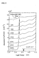
- FIG. 2 shows temperature dependence of optical absorption spectra in the temperature range of 10 K to 300 K. A sharp absorption originated from exciton could be observed.
- an optical absorption spectrum at 6 K of a LaCuOS polycrystal film is also shown in FIG. 2.
- An emission light was converged by a lens, and led to an optical fiber bundle. Then, the emission was spectrally divided to measure emission spectrum using a mono equip a charge-coupled device (CCD).
- the excitation was performed by irradiating the third harmonics (wavelength: 266 nm) of neodimium doped yttrium aluminum garnet (Nd : YAG) laser onto the thin film.
- FIG 3 shows the emission spectra in the temperature range of 10 K to 300 K. A sharp ultraviolet emission having a center wavelength of 390 nm could be observed.
- Y 2 O 3 single-crystal thin film was grown on an YSZ (100) single-crystal substrate (10 mm square ⁇ 0.5 mm thickness) through a PLD process at a substrate temperature of 900°C.
- the thickness of the Y 2 O 3 thin film determined by on an X-ray reflectance measurement was 35 nm.
- the crystallinity of the grown Y 2 O 3 single-crystal thin film was evaluated using a HRXRD system. As a result, Y 2 O 3 was oriented toward the (100) plane on the YSZ (100) single-crystal substrate, and the tilt angle was 0.5-degree. Through an in-plane measurement, it was verified that the prepared Y 2 O 3 thin film is epitaxially grown. The epitaxial relationship is clarified as follows. Y 2 O 3 (100) // YSZ (100) Y 2 O 3 (010) // YSZ (010)
- Cu thin film was grown on the Y 2 O 3 /YSZ single-crystal substrate.
- the crystallinity of the grown Cu thin film was evaluated using a HRXRD system.
- Cu was oriented toward the (111) plane on the Y 2 O 3 (100)/YSZ (100) substrate, and the tilt angle was 0.01-degree.
- LaCuOS was deposited on the Cu thin film grown on the Y 2 O 3 /YSZ single-crystal substrate as a base layer while maintaining the substrate at room temperature, through a pulsed laser deposition process (PLD process) under the same conditions as those in Inventive Example 1-2. Through an X-ray reflectance measurement, it was proved that the thickness of an obtained LaCuOS thin film is 200 nm.
- the prepared LaCuOS thin film was amorphous.
- the crystallinity of the prepared single-crystal thin film was checked using a HRXRD system (ATX-G available from Rigaku; radiation source: Cu-K ⁇ 1 ).
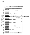
- An out-of-plane pattern is shown in FIG 4. Y 2 O 3 and Cu or LaCuOS were not reacted. Further, any diffraction of the Cu thin film used as the base thin film disappeared. A strong diffraction peak from the (001) plane of LaCuOS was observed together with Y 2 O 3 (100) and YSZ (100) peaks.
- the out-of-plane pattern shows that LaCuOS (001) is strongly oriented on Y 2 O 3 (100). According to a rocking curve measurement, the tilt angle of the LaCuOS (001) plane was 0.1-degree.
- LaCuOS was deposited on the Cu thin film grown on the MgO (100) single-crystal substrate as a base layer while maintaining the substrate at room temperature, through a pulsed laser deposition process (PLD process) under the same conditions as in Inventive Example 1-2.
- the deposited LaCuOS thin film was amorphous.
- LaCuOSe was deposited on the LaCuOS/Cu/MgO laminated film while maintaining the substrate at room temperature, through a pulsed laser deposition process (PLD process) using a LaCuOSe sintered body as a target under a high vacuum atmosphere ( ⁇ 10 -5 Pa).
- PLD process pulsed laser deposition process
- the LaCuOSe thin film deposited on the LaCuOS thin film was amorphous.
- An YSZ (100) substrate material was attached onto each of the surfaces of the three kinds of LaCuOSe/LaCuOS/Cu/MgO laminated films, the LaCuOS/Cu/MgO laminated film and the LaCuOSe/Cu/MgO laminated film.
- each of the laminated film was enclosed in a vacuumized and sealed quartz glass tube together with LaCuOS powder and LaCuOSe powder (each mean particle size of about 0.1 mm; each weight of about 0.1 g). Then, the quartz tube was heated in an ambient pressure at 1000°C for 6 hours. After the heat treatment, the laminated film was cooled to room temperature in a furnace.
- the emission characteristic was evaluated in the same manner as in Inventive Example 1-5.
- a single-crystal LaCuOS thin film was grown on an YSZ (100) single-crystal substrate. According to an X-ray reflectance measurement, the thickness of the LaCuOS thin film was 140 nm.
- LaCuOSe was deposited on the single-crystal LaCuOS thin base film while maintaining the substrate at room temperature, through a PLD process using a LaCuOSe sintered body as a target under a high vacuum atmosphere ( ⁇ 10 -5 Pa). According to an X-ray reflectance measurement, the thickness of the LaCuOSe thin film was 60 nm. The deposited LaCuOSe thin film was amorphous.
- LaCuOSe/LaCuOS/YSZ laminated films Two LaCuOSe/LaCuOS/YSZ laminated films were prepared, and the respective surfaces thereof were attached together.
- the laminated films were enclosed in a vacuumized and sealed quartz glass tube together with LaCuOS powder and LaCuOSe powder (each mean particle size of about 0.1 mm; and weight of about 0.1 g). Then, the sealed quartz tube was heated in a ambient atmosphere at 1000°C for 6 hours. After the heat treatment, the laminated films were cooled to room temperature in a furnace.
- the crystallinity of each of the prepared single-crystal thin films was checked using a HRXRD system (ATX-G available from Rigaku; radiation source: Cu-K ⁇ 1 ).
- An out-of-plane pattern is shown in FIG. 7.
- the pattern of a LaCuOS single-crystal thin film is also shown in FIG 7.
- a thin film was deposited on an YSZ (100) single-crystal substrate at a substrate temperature of 500 to 900°C through a PLD process using a LaCuOS sintered body as a target under an H 2 S atmosphere.
- the composition of the thin film was analyzed by an X-ray fluorescence measurement. As a result, it was proved that a La/Cu atomic ratio shows a tendency to increase as the substrate temperature is increased, and the concentration of S in the thin film shows a tendency to decrease as the substrate temperature is increased. From of these data, it may conclude that the sublimation of the components Cu and S having a high vapor pressure occurred with the increase in the substrate temperature. As a result of an XRD measurement for the deposited thin film, any pattern representing a single phase of LaCuOS was not found.
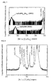
- FIG. 8 shows an XRD pattern of a film deposited through a PLD process at a substrate temperature of 500°C under an H 2 S atmosphere as an example.
- peaks for La 2 O 3 and La 2 O 2 S are observed. This result is consistent with the result of the composition analysis that concentration of La in the film is higher as compared to Cu.
- concentration of La in the film is higher as compared to Cu.
- a thin film was deposited on an YSZ (100) single-crystal substrate at a substrate temperature of 500 to 900°C through a PLD process using a LaCuOS sintered body as a target.
- the obtained thin film was enclosed in a vacuum capsule, and then subjected to a heat treatment at 1000°C for 30 minutes. After the completion of the heat treatment, the thin film was cooled to room temperature in a furnace. Through a HRXRD measurement for the prepared thin film, it was verified that the obtained thin film was a single-phase polycrystalline LaCuOS.
- FIG 9 shows respective XRD patterns with the Cu thin film and without Cu thin film.
- the LnCuOX single-crystal thin film of the present invention is suitable to substrate black for light-emitting diodes, semiconductor lasers, field-effect transistors or hetero-bipolar transistors.
Landscapes
- Chemical & Material Sciences (AREA)
- Engineering & Computer Science (AREA)
- Crystallography & Structural Chemistry (AREA)
- Materials Engineering (AREA)
- Metallurgy (AREA)
- Organic Chemistry (AREA)
- Inorganic Chemistry (AREA)
- Physics & Mathematics (AREA)
- Thermal Sciences (AREA)
- Crystals, And After-Treatments Of Crystals (AREA)
- Physical Deposition Of Substances That Are Components Of Semiconductor Devices (AREA)
- Recrystallisation Techniques (AREA)
- Led Devices (AREA)
- Luminescent Compositions (AREA)
- Physical Vapour Deposition (AREA)
Abstract
Description
- The present invention relates to a method of producing an LnCuO(S, Se, Te) single-crystal thin film (wherein Ln is at least one selected from the group consisting of lanthanide elements and yttrium (Y)), a single-crystal thin film obtained through the production method, and an optical or electronic device using the single-crystal thin film.
- Vapor-phase epitaxial growth means that, when a deposited film is grown on a single-crystal substrate in a vacuum atmosphere, the growth proceeds while maintaining a given relationship between the respective crystal orientations of the substrate and the deposited film under the influence of the orderly atomic arrangement of the crystal of the substrate. A typical thin film growth technology based on the epitaxial growth includes a sputtering process, a chemical vapor deposition (CVD) process, a molecular beam epitaxy (MBE) process and a pulsed laser deposition (PLD) process.
- Currently, the sputtering process using non-equilibrium evaporation is most widely used and industrially applied. A sputtering process for use as a film forming method utilizes a so-called sputtering-phenomenon discovered by W. Grove in 1852. The sputtering phenomenon means that high-kinetic energy particles emitted onto the surface of a target (ions or atoms neutralized by electrons around the target surface) give the kinetic momentum of the particles to constitutive atoms of the target through an elastic collision therebetween, and the recoil atoms are finally released from the target surface after repeatedly colliding with adjacent atoms. The film forming method based on the sputtering process is intended to deposit the released constitutive atoms of the target on a substrate so as to form a thin film.
- The chemical vapor deposition (CVD) process is intended to grow a thin film having a desired composition on a substrate by using chloride or organometal compound as a source material, and inducing the chemical reaction between source gases on the substrate. The CVD process having excellent compatibility to mass production is widely used to produce practical materials for semiconductor lasers and others.
- The molecular beam epitaxy (MBE) process is a thin-film crystal growth technology named in 1968 by J. R. Arthur who was with Bell Laboratory at the time, and developed for compound semiconductors, primarily GaAs. The MBE process can be considered as an improved or progressive type of a vacuum deposition process.
- Specifically, the MBE process is intended to perform an epitaxial crystal growth under the conditions that the flow of neutral molecules (or atoms) serving as raw materials of a crystal to be grown, or the intensity of a molecular beam (atomic beam), is accurately controlled in ultra-high vacuum, and the neutral molecules (or atoms) are emitted onto an accurately temperature-controlled substrate. The MBE process can be applied to a wide range of materials including compound semiconductors, elementary semiconductors such as Si, and various metal or oxide superconductors. The difference from the conventional vacuum deposition process is in that (i) the vacuum degree in a growth chamber is set at 10-7∼10-8 Pa or less, (ii) the crystal growth is performed while stably maintaining the cleanness of the crystal surface at the atomic scale, and (iii) the intensity of the molecular beam is accurately controlled.
- The research and development of the pulsed laser deposition (PLD) process was started soon after the first success in ruby laser oscillation in 1960. From the last half of the 1980s, the pulsed laser deposition (PLD) process using an excimer laser has been actually applied to a production method for a single-crystal thin film of high-temperature superconducting material, dielectric material or organic polymer
- Laser ablation means a process of etching the surface of a solid utilizing a phenomenon that when the intensity of laser light emitted onto a solid is increased up to a given threshold value or more, the laser light is converted into electronic, thermal, photochemical and mechanical energies on the solid surface, and consequently various kinds of fragments (neutral atoms, molecules, positive/negative ions, radicals, clusters, etc.) are explosively released from the solid surface.
- The PLD process utilizes the principle of the laser ablation to produce a single-crystal thin film on a substrate under an ultra-high vacuum atmosphere set at a vacuum degree of 10-7∼10-8 Pa or less in a growth chamber, or under a sufficiently controlled atmosphere based on the flow of reactive gas. While the PLD process is a non-equilibrium process as with the sputtering process, it is different from the sputtering process in that the difference between the respective compositions of a target and an obtained film is small, and single-crystal films of various material can be produced by simply replacing a target. In recent years, the PLD process is actively used, particularly, in the field of research on exploration of substances, by utilizing the above features.
- The present invention is directed to the development of a technique for achieving LnCuOX epitaxial single-crystal thin film growth (wherein Ln is at least one selected from the group consisting of lanthanide elements and yttrium (Y), and X is at least one selected from the group consisting of S, Se and Te) by use of a solid-phase epitaxial process. It has been verified that LnCuOX exhibits luminescence or light-emission originated from excitons even in a polycrystalline film thereof. Therefore, LnCuOX has much promise as materials for light-emitting devices. For example, if an LnCuOX single-crystal thin film is obtained, it can be used as a material of ultraviolet light-emitting devices. However, in case of using a film forming method performed in a vacuum atmosphere at high temperatures, it is difficult to obtain even a single-phase LnCuOX thin film, because the Cu compound and X component contained in LnCuOX as the constitutive elements thereof have a high vapor pressure.
- LnCuOX is a wide-bandgap p-type semiconductor. Generally, most of wide-bandgap substances, such as ZnO and SnO2, can not exhibit both n- and p-types conductively but an n-type semiconductor having electrons as a main carrier. Thus, if a Field Effect Transistor (FET) structure is formed using such substances, a gate operating voltage will be positive. Whereas, if the same FET structure is constructed using LnCuOX which is a wide-bandgap p-type semiconductor, a gate operating voltage will be negative. Therefore, a wide-bandgap Complementary Metal-Oxide Semiconductor (CMOS) circuit, or a high-performance transparent electronic circuit, can be produced by combining this p-type wide-bandgap semiconductor FET with the aforementioned n-type wide-bandgap semiconductor FET. Otherwise, the p-type wide-bandgap semiconductor can also be combined with an n-type semiconductor to produce a hetero-junction bipolar transistor or light-emitting diode using a p-n junction.
- In 1981, the existence of layer-structured oxysulfide LaCuOS was first reported by Palazzi (M. Palazzi, Acad. Sci. Paris C. R. 292, 789 (1981)). The crystal system of LaCuOS is a tetragonal system with the space group No. 129, P4/nmm, wherein the Z value = 2, and the lattice parameters: a = 3.999 Å, c = 8.53 Å. LaCuOS has a layer structure in which a (La2O2)2+ layer and a (Cu2S2)2- layer are alternately stacked along the c-axis of the tetragonal system.
- In 2000, K. Ueda et al. first reported that LaCuOS is a transparent p-type semiconductor having a bandgap of about 3.1 eV which suggests promise as a next-generation wide-bandgap p-type semiconductor material (K. Ueda, S. Inoue, S. Hirose, H. Kawazoe and H. Hosono, Appl. Phys. Lett., 77, 2701 (2000)).
- In 2001, K. Ueda et al. reported that LaCuOS exhibits exciton-originated optical absorption/emission characteristics having stability even at room temperature, and has promise as a next-generation material of ultraviolet light-emitting devices (K. Ueda, S. Inoue, H. Hosono, N. Sarukura and M. Hirano, Appl. Phys. Lett., 78, 2333 (2001)).
- As is generally known, even if the La site of LaCuOS is substituted with another lanthanide element or the S site of LaCuOS is substituted with another chalcogen element, i.e. Se or Te, the same crystal structure will be maintained. It has also been reported that these are synthesized in a similar way (D. O. Charkin, A. V. Akopyan and V. A. Dolgikh, Russian J. Inorg. Chem., 44, 833 (1999)). Therefore, with respect to all kinds of LnCuOX, a single-crystal thin film can be grown in basically the same techniques.
- It is known that the electrical conductivity of LnCuOX is increased up to about 102 S/cm by substituting the Ln site with divalent alkali earth metal ions of Sr and Ca (K. Ishikawa, S. Kinoshita, Y. Suzuki, S. Matsuura, T. Takanishi, M. Aizawa and Y. Suzuki, J. Electrochem. Soc. 138, 1166 (1991), and Y. Takano, K. Yahagi and K. Sekizawa, Physica A 206&207, 764 (1995)). It has also been reported that even an LnCuOX polycrystal thin film with the Ln site substituted with Sr has an electrical conductivity increased from 6.4 × 10⁻⁵ S/cm up to 20 S/cm, and a maximum hole concentration increased up to 2.7 × 1020 cm-3 (Reference: H. Hiramatsu, M. Orita, M. Hirano, K. Ueda and H. Hosono, J. Appl. Phys. 91, 9177(2002)).
- LaCuOS and LaCuOSe prepared by substituting the S site of LaCuOS with Se exhibit complete solid solubility therebetween, and form a solid solution LaCuOS1-x Sex (0 < x < 1) (K. Ueda and H. Hosono, Thin Solid Films, 411, 115 (2002)). It is known that the bandgap of the LaCuOS1-x Sex can be controllably changed from 3.1 eV to 2.8 eV by continuously varying the value x representing the amount of substitution from zero to 1 (K. Ueda and H. Hosono, J. Appl. Phys. 91, 4768 (2002)). Thus, a LaCuOS1-x Sex film prepared by accurately controlling the value x and the thickness thereof can have a desirably controlled light-emission wavelength. It is also possible to form quantum well structure using the mixed compounds.
- While LnCuOX is a wide-bandgap p-type semiconductor and it is expected to be applicable to the active layer of an ultraviolet light-emitting device, it was very difficult to produce a single-crystal thin film thereof. Heretofore, a LnCuOX thin film has been produced by annealing an amorphous film at a high temperature which were deposits by a sputtering process under appropriate conditions, (K. Ueda, S. Inoue, S. Hirose, H. Kawazoe and H. Hosono, Appl. Phys. Lett. 77, 2701 (2000)).
- However, a film produced by the above method was unexceptionally a polycrystalline from incapable of achieving high light-emission efficiency and large electron mobility required for a material of light-emitting devices or electronic devices. Thus, it has been strongly desired to develop a single-crystal thin film production method capable of effectively growing a thin film excellent in crystallinity so as to allow LnCuOX to be practically used as a light-emitting material or a p-type conductive semiconductor.
- In order to solve the above mentioned problems, the present invention provides a method of producing an LnCuOX single-crystal thin film (wherein Ln is at least one selected from the group consisting of lanthanide elements and yttrium, and X is at least one selected from the group consisting of S, Se and Te). The method comprises the steps of growing a base thin film on a single-crystal substrate, depositing an amorphous or polycrystalline LnCuOX thin film on the base thin film to form a stacked film, setting the bi-layered film in a vacuum, and then annealing the stacked film at a high temperature of 500°C or more in the vacuum to grow an LnCuOX single-crystal thin film.
- Initially very thin film of the LnCuOX single-crystal is formed on a film which serves as the base film. In this reaction process, if either one of Cu, Cu2S, CuS, Cu2O, CuO, CuCl, CuCl2 and CuI films is used as the base thin film, the component Cu, O or S of the base thin film will be mixed in LnCuOX, and Ce or I is vanished by the vaporization, and thereby LnCuOX will be epitaxially grown directly on the single-crystal substrate made of either one of YSZ (Yttria-Stabilized Zirconia), Y2O3, STO (strontium titanate), Al2O3 and MgO, on which the base thin film is grown.
- Otherwise, if either one of an Ag film, an Ag compound film such as an Ag2S, Ag2O, AgO, AgCl or AgI film, and an Au film is used as the base thin film, instead of the Cu, Cu2S, CuS, Cu2O, CuO, CuCl, CuCl2 or CuI film, the components of the base thin film will be entirely left on the single-crystal substrate made of either one of YSZ, Y2O3, STO, Al2O3 and MgO, or will be partially diffused in LnCuOX and left therein as impurities.
- In the method of the present invention, the stacked film composed of the amorphous or polycrystalline LnCuOX thin film and the base thin film on the single-crystal substrate is annealed while enclosing the film in a vacuum environment, vacuum sealed capsule for example, so as to prevent the components Cu and X from being vaporized during a heating treatment.
- The LnCuOX single-crystal thin film produced in this manner can be used as the active layer of an ultraviolet light-emitting device (diode or laser) by taking advantage of its high light-emission efficiency at room temperature associated with exciton. The LnCuOX single-crystal thin film can be used as a channel layer of a field-effect transistor (FET) to produce a transparent FET to be operated at a negative gate voltage. The FET device combined with n-channel FET to produce a CMOS circuit or a hetero-bipolar device.
-
- FIG. 1 is a graph showing an out-of-plane XRD pattern representing the crystallinity of an LnCuOX single-crystal thin film produced in Inventive Example 1.
- FIG. 2 is a graph showing an optical-absorption spectrum in the temperature range of 10 to 300 K of the LnCuOX single-crystal thin film produced in Inventive Example 1.
- FIG. 3 is a graph showing a photo-emission spectrum in the temperature range of 10 to 300 K of the LnCuOX single-crystal thin film produced in Inventive Example 1.
- FIG. 4 is a graph showing an out-of-plane XRD pattern representing the crystallinity of an LnCuOX single-crystal thin film produced in Inventive Example 2.
- FIG. 5 is a graph showing an out-of-plane XRD pattern of a LaCuOS1-xSex (x = 0, 0.25, 0.4, 0.7, 1.0) produced in Inventive Example 3.
- FIG. 6 is a graph showing a photo-emission spectrum at 10 K of a LaCuOS1-xSex (x = 0, 0.25, 0.4, 1.0) produced in Inventive Example 3.
- FIG. 7 is a graph showing an out-of-plane XRD pattern representing the crystallinity of a single-crystal LnCuOXX' solid-solution thin film produced in Inventive Example 4.
- FIG. 8 is a graph showing an out-of-plane XRD pattern representing the crystallinity of an LnCuOX film produced in Comparative Example 1.
- FIG 9 is a graph showing out-of-plane XRD patterns for comparing the respective crystallinities of the LnCuOX film produced in Comparative Example 1 and an LnCuOX thin film produced using a Cu base thin film.
-
- In a method of producing an LnCuOX single-crystal thin film, according to the present invention, a base thin film may be grown appropriately using a conventional film forming method, such as a sputtering process, a CVD process, a MBE process or a PLD process. A single-crystal substrate for use in the method may be made of either one of YSZ, Y2O3, STO, Al2O3 and MgO. In particular, a YAS (100), Y2O3 (100) or MgO (100) single crystal is preferably used as the single-crystal substrate, because they have no risk of causing a chemical reaction with an LnCuOX compound even at a high temperature of 1200°C or less.
- More specifically, it is desirable to use a single-crystal substrate in which the anion-anion nearest-neighbour distance in the substrate crystal plane (A-substrate) is close to the anion-anion nearest-neighbour distance in the C plane of LnCuOX (A-film), or which has less lattice mismatch. For example, the A-substrate is 2.82 for LaCuOS, 2.88 for LaCuOSe, 2.96 for MgO(100), 2,58 for YSZ(100), and 2.92 for Y2O3 (100). Thus, in case of growing a LaCuOS•Se single-crystal thin film, Y2O3, MgO and YSZ have a higher priority for the single-crystal substrate in this order, in view of the lattice mismatch.
- In the initial process of the film growth , a base thin film made of either one material selected from the group consisting of Cu, Cu2S, CuS, Cu2O, CuO, CuCl, CuCl2, CuI, Ag, Ag2S, Ag2O, AgO, AgCl, AgI and Au, is grown on the single-crystal substrate, such as an YSZ, Y2O3 or MgO single-crystal substrate. If the base thin film is made of Cu or Cu-based compound, the components Cu, O and/or S of the base thin film will be mixed in an LnCuOX thin film to be deposited onto the base thin film. Whereas, if the base thin film is made of a material other than Cu or Cu-based compound, the components of the base thin film will be left on the interface between the single-crystal substrate and the LnCuOX thin film, or partially diffused into the LnCuOX thin film.
- Then, an LnCuOX thin film is deposited on the base thin film by using an LnCuOX sintered body as a target, under an H2S atmosphere when LnCuOX is LnCuOS, or under an argon or vacuum atmosphere when LnCuOX is LnCuOSe or LnCuOTe. While a sputtering process or a PLD process is preferably used for depositing the LnCuOX thin film in view of their simplicity, the present invention is not limited to such process. The LnCuOX thin film to be deposited on the base thin film may be polycrystalline or may be amorphous.
- Alternatively, a solid-solution film may be deposited on the base thin film by using an LnCuOX1-xX'x (each of X and X' is at least one selected from the group consisting of S, Se and Te, wherein X and X' are different elements; 0 < x < 1) solid-solution sintered body as a target. In this case, a single-crystal film having the above solid-solution composition is obtained as a final product. Otherwise, a stacked of film different in composition may be deposited in the form of multilayer by using two kinds of targets different in Ln or X. In this case, a solid-solution single-crystal thin film having a composition which is a film-thickness-weighted average of all of the film compositions is obtained as a final product.
- The solid solution LnCuOX1-xX'x is useful as a light-emitting material because the light-emission wavelength thereof can be continuously changed by controlling the value of x. In addition, the forbidden band or energy gap of the solid solution LnCuOX1-xX'x is continuously changed depending on the value of x. Thus, artificial superlattice structures is formed by alternately laminating single-crystal films different in the value of x.
- Laminated film composed of the LnCuOX thin film and the base thin film on the single-crystal substrate is enclosed in a vacuum environment, such as in sealed vacuum capsule, and subjected to a heat treatment at a temperature of 500°C or more, preferably 1000°C or more. Under the condition of less than 500°C, any homogeneous single-crystal LnCuOX thin film cannot be obtained due to insufficient diffusion. On the other hand, when a heating temperature is 1200°C or more the undesirable reaction between the single-crystal substrate and the LnCuOX compound takes place. Further, the softening of quartz glass make it unusability as a material to form sealed vacuum capsule.
- The components Cu and X have a high vapor pressure. Thus, if the laminated film is annealed at a high temperature under a vacuum atmosphere, a high-quality LnCuOX single crystal cannot be obtained in some cases, due to significant change in the composition of the thin film obtained after the heat treatment, due to vaporization of the components Cu and X from the LnCuOX thin film. In order to suppress the vaporization of the components Cu and X, in advance of the heating treatment, the laminated film is enclosed in such a vacuum environment as typically enclosed in a quartz tube which is vacuumized and then hermetically sealed.
- Furthermore, in order to suppress very slight evaporation of Cu and X, annealing may be carried out in an atmosphere containing LnCuOX vapor, generating in the vacuum sealed chamber LnCuOX vapor having the same chemical formula as that of the single-crystal thin film, compensating the vapor pressure of Cu and X in the vacuum sealed and heated atmosphere. For example, this may be achieved in such a way that LnCuOX powder is enclosed in the closed vacuum environment together with the laminated film.
- In case of using the LnCuOX powder, the LnCuOX vapor generated during the heating treatment is solidified in the form of particles, and the particles are likely to be deposited on surface of the single-crystal thin film so as to cause the roughened surface thereof. In order to prevent this problem, before the laminated film is enclosed in the vacuum environment, the surface of the LnCuOX thin film may be covered by plate, such as YSZ plate, which has no reactivity with the LnCuOX thin film.
- The vaporization of the components Cu and X may also be suppressed by preparing an additional laminated film composed of the LnCuOX thin film and the base thin film on the single-crystal substrate, attaching the respective surfaces of the aforementioned laminated film and the additional laminated film together, and then enclosing these laminated films in the vacuum environment. The above additional film may be composed of the LnCuOX thin film on the single-crystal substrate without the base thin film. In this case, only the laminated film having the base thin film will be formed as the LnCuOX single-crystal thin film.
- As with polycrystals, the Ln site of LnCuOX can be substituted with a divalent ion of a metal M (M is at least one selected from the group consisting of Mg, Ca, Sr, Ba and Zn) to effectively create hole carriers. In this case, the divalent metal ion may be contained in a sintered body target to substitute the Ln site of the LnCuOX thin film with the divalent metal ion. The amount of the substitution may be varied to continuously change the electrical conductivity of an Ln1-yMyCuOX single-crystal thin film (wherein 0 < y < 1) from 10-5 S/cm to 80 S/cm.
- A combination of the single-crystal substrate and the LnCuOX thin film having a large lattice mismatch therebetween is likely to cause difficulties in growing a single-crystal film. For example, when a LaCuOS1-xSex film having x of 0.5 or more is grown on a (100) plane of an YSZ substrate, it is difficult to obtain a single-crystal film. Even in such a case, a single-crystal LaCuOS1-xSex solid-solution thin film can be obtained by growing an LnCuOX single-crystal thin film having less lattice mismatch on a (100) plane of an YSZ substrate through the aforementioned process, depositing an LnCuOSe thin film on the LnCuOX single-crystal thin film to form a laminated film, and annealing the laminated film at a high temperature of 500°C while enclosing the laminated film in a vacuum environment. That is, an amorphous or polycrystalline LnCuOX' is solid-phase diffused into the LnCuOX single-crystal thin film to grow an LnCuOX1-xX'x single-crystal thin film having large lattice mismatch with the single-crystal substrate. In this case, the Ln site of the LnCuOX single-crystal thin film may be substituted with a divalent ion of the metal M.
- The solid solution LnCuOX1-xX'x is useful as a material for light emitting devices because the light-emission wavelength thereof can be continuously changed by controlling the value of x. In addition, the forbidden band or energy gap of the solid solution LnCuOX1-xX'x is continuously changed depending on the value of x. Thus, alternate lamination of single-crystal films different in the value of x may result in the formation of an artificial superlattice structure.
- The LnCuOX single-crystal thin film or the Ln1-yMyCuOX single-crystal thin film obtained in this manner can be laminated to an n-type semiconductor consisting of either one of ZnO, ZnS, In2O3 and SnO2 to form a PN heterojunction structure so as to produce a light-emitting diode.
- The LnCuOX single-crystal thin film or the Ln1-yMyCuOX single-crystal thin film can also be combined with ZnO or ZnO : Mg to form a double hetero structure so as to produce a semiconductor laser.
- Further, the LnCuOX single-crystal thin film or the Ln1-yMyCuOX single-crystal thin film can be used to fabricate a FET by depositing YSZ thereon as a gate insulation film, and depositing Pt-Pd or ITO (Indium-Tin Oxide) thereon as source and drain electrodes.
- Furthermore, the LnCuOX single-crystal thin film or the Ln1-yMyCuOX single-crystal thin film can be used to fabricate a hetero-bipolar transistor by combining with an n-type semiconductor consisting of either one of ZnO, ZnS, In2O3 and SnO2 to form a hetero structure, and forming an ohmic electrode on each of the surfaces of the hetero structure.
- The present invention will be described in more detail in connection with the following examples.
- Cu thin film was grown on an YSZ (100) single-crystal substrate (10 mm square × 0.5 mm thickness) through a PLD process at a substrate temperature of 200°C. The thickness of the Cu thin film determined by X-ray reflectance and X-ray fluorescence measurements was 5 nm. The crystallinity of the grown Cu thin film was evaluated using a HRXRD (High-Resolution X-Ray Diffraction) system. As a result, Cu was oriented toward the (111) plane of the YSZ (100) single-crystal substrate, and the tilt angle was 0.01-degree.
- LaCuOS was deposited on the Cu thin film grown on the YSZ (100) single-crystal substrate as a base layer while maintaining the substrate at room temperature, through a pulsed laser deposition process (PLD process) under an H2S atmosphere using a LaCuOS sintered body as a target. Through an X-ray reflectance measurement, it was proved that the thickness of an obtained LaCuOS thin film is 200 nm. The deposited LaCuOS thin film was amorphous.
- Two of the LaCuOS/Cu/YSZ laminated films were prepared, and the respective surfaces of the laminated films were attached together. In order to suppress the vaporization of the components Cu and S of the LaCuOS thin film having a high vapor pressure, the laminated films were enclosed in a vacuumized and sealed quartz glass tube together with LaCuOS powder (mean particle size of about 0.1 mm; about 0.1 g). Then, the sealed quartz tube capsule was annealed by heating in an ambient atmosphere at 1000°C for 30 minutes. After the heat treatment, the laminated films were cooled to room temperature in a furnace.
- The crystallinity of the obtained LaCuOS single-crystal thin film was checked using a HRXRD system (ATX-G available from Rigaku; radiation source: Cu-Kα1). An out-of-plane pattern is shown in FIG. 1. A strong diffraction peak from the (001) plane of LaCuOS was observed together with an YSZ (100) peak. The out-of-plane pattern shows that LaCuOS (001) is strongly oriented on YSZ (100). According to a rocking curve measurement, the tilt angle of the LaCuOS (001) plane was 0.1-degree. Any diffraction due to the Cu thin film used as the base thin film disappeared. Based on the in-plane measurement, it was verified that the prepared LaCuOS thin film is epitaxially grown. The epitaxial relationship is channeled as follows.
- 5. Optical-Absorption and Emission Characteristics of LaCuOS Single-Crystal Thin Film. The obtained LaCuOS single-crystal thin film was attached to a cryostat (4.2 K; available from Daikin). The interior space of the system was evacuated, and then cooled to 10 K. FIG 2 shows temperature dependence of optical absorption spectra in the temperature range of 10 K to 300 K. A sharp absorption originated from exciton could be observed. As a comparative example, an optical absorption spectrum at 6 K of a LaCuOS polycrystal film is also shown in FIG. 2.
- An emission light was converged by a lens, and led to an optical fiber bundle. Then, the emission was spectrally divided to measure emission spectrum using a mono equip a charge-coupled device (CCD). The excitation was performed by irradiating the third harmonics (wavelength: 266 nm) of neodimium doped yttrium aluminum garnet (Nd : YAG) laser onto the thin film. FIG 3 shows the emission spectra in the temperature range of 10 K to 300 K. A sharp ultraviolet emission having a center wavelength of 390 nm could be observed.
- An Y2O3 single-crystal thin film was grown on an YSZ (100) single-crystal substrate (10 mm square × 0.5 mm thickness) through a PLD process at a substrate temperature of 900°C. The thickness of the Y2O3 thin film determined by on an X-ray reflectance measurement was 35 nm. The crystallinity of the grown Y2O3 single-crystal thin film was evaluated using a HRXRD system. As a result, Y2O3 was oriented toward the (100) plane on the YSZ (100) single-crystal substrate, and the tilt angle was 0.5-degree. Through an in-plane measurement, it was verified that the prepared Y2O3 thin film is epitaxially grown. The epitaxial relationship is clarified as follows.
- In the same preparation process as in Inventive Example 1-1, Cu thin film was grown on the Y2O3/YSZ single-crystal substrate. The crystallinity of the grown Cu thin film was evaluated using a HRXRD system. As a result, Cu was oriented toward the (111) plane on the Y2O3 (100)/YSZ (100) substrate, and the tilt angle was 0.01-degree.
- LaCuOS was deposited on the Cu thin film grown on the Y2O3/YSZ single-crystal substrate as a base layer while maintaining the substrate at room temperature, through a pulsed laser deposition process (PLD process) under the same conditions as those in Inventive Example 1-2. Through an X-ray reflectance measurement, it was proved that the thickness of an obtained LaCuOS thin film is 200 nm. The prepared LaCuOS thin film was amorphous.
- In the same manner as in Inventive Example 1-3, a single-crystal LaCuOS thin film was prepared.
- The crystallinity of the prepared single-crystal thin film was checked using a HRXRD system (ATX-G available from Rigaku; radiation source: Cu-Kα1). An out-of-plane pattern is shown in FIG 4. Y2O3 and Cu or LaCuOS were not reacted. Further, any diffraction of the Cu thin film used as the base thin film disappeared. A strong diffraction peak from the (001) plane of LaCuOS was observed together with Y2O3 (100) and YSZ (100) peaks. The out-of-plane pattern shows that LaCuOS (001) is strongly oriented on Y2O3 (100). According to a rocking curve measurement, the tilt angle of the LaCuOS (001) plane was 0.1-degree.
- Example of growing Single-Crystal LaCuOS1-xSex (0 < x < 1) Solid-Solution Thin Film on Substrate having Small Lattice Mismatch
- In the same preparation process as in Inventive Example 1-1, Cu thin film was grown on an MgO (100) single-crystal substrate. The crystallinity of the prepared Cu thin film was evaluated using a HRXRD system. As a result, Cu was oriented toward the (001) plane on the MgO (100) substrate, and the tilt angle was 0.01-degree.
- LaCuOS was deposited on the Cu thin film grown on the MgO (100) single-crystal substrate as a base layer while maintaining the substrate at room temperature, through a pulsed laser deposition process (PLD process) under the same conditions as in Inventive Example 1-2. The deposited LaCuOS thin film was amorphous.
- LaCuOSe was deposited on the LaCuOS/Cu/MgO laminated film while maintaining the substrate at room temperature, through a pulsed laser deposition process (PLD process) using a LaCuOSe sintered body as a target under a high vacuum atmosphere (∼ 10-5 Pa). The LaCuOSe thin film deposited on the LaCuOS thin film was amorphous.
- The above processes from 3-1 to 3-3 were repeated to prepare three kinds of LaCuOSe/LaCuOS/Cu/MgO laminated films different in the combination of the thicknesses of the LaCuOSe and LaCuOS thin films. Further, in the same manner as in Inventive Example 1, a laminated film without the LaCuOS thin film and a laminated film without the LaCuOSe thin film were prepared. The respective film thicknesses are shown as follows.
(Amorphous LaCuOS film thickness) : (Amorphous LaCuOSe film thickness)
= (200 : 0), (150 : 50), (120 : 80), (60 : 140), (0 : 200) - An YSZ (100) substrate material was attached onto each of the surfaces of the three kinds of LaCuOSe/LaCuOS/Cu/MgO laminated films, the LaCuOS/Cu/MgO laminated film and the LaCuOSe/Cu/MgO laminated film. In order to suppress the vaporization of the components Cu, S and Se having a high vapor pressure, each of the laminated film was enclosed in a vacuumized and sealed quartz glass tube together with LaCuOS powder and LaCuOSe powder (each mean particle size of about 0.1 mm; each weight of about 0.1 g). Then, the quartz tube was heated in an ambient pressure at 1000°C for 6 hours. After the heat treatment, the laminated film was cooled to room temperature in a furnace.
- The crystallinity of each of the grown single-crystal thin films was checked using a HRXRD system (ATX-G available from Rigaku; radiation source: Cu-Kα1). An out-of-plane pattern is shown in FIG 5. Strong diffraction peaks for the (003) and (004) planes of LaCuOS1-xSex (x = 0, 0.25, 0.4, 0.7, 1.0) were observed together with an MgO (200) peak. The out-of-plane pattern shows that all of LaCuOS1-xSex (x = 0, 0.25, 0.4, 0.7, 1.0) are strongly oriented on YSZ (100). Further, it is proved that the length of the c-axis of the crystal is expanded (corresponding to shift of diffraction peak toward a lower angle side) as Se is dissolved into the S site to form a solid solution. Based on the in-plane measurement, it was verified that all of the growth LaCuOS1-xSex (x = 0, 0.25, 0.4, 0.7, 1.0) thin films are epitaxially grown. The epitaxial relationship is shown as follows.
- The emission characteristic was evaluated in the same manner as in Inventive Example 1-5. FIG 6 shows emission spectra at room temperature. A sharp emission line originated from exciton was observed. The emission wavelength was shifted toward a longer wavelength side as the concentration of Se is increased. The concentration of substituted Se can be accurately controlled to continuously change the emission wavelength from 390 nm (x = 0) to 430 nm (x = 1) at room temperature.
- As above, when the MgO (100) substrate having small lattice mismatch is used, a single crystal LaCuOS1-xSex (0 < x < 1) solid-solution thin film could be epitaxially grown on the substrate according to the method as shown in this example.
- Example of growing Single-Crystal LnCuOX1-xX'x (0 < x < 1) Solid-Solution Thin Film on Substrate having Large Lattice Mismatch
- In the same manner as in Inventive Example 1-1 to 1-4, a single-crystal LaCuOS thin film was grown on an YSZ (100) single-crystal substrate. According to an X-ray reflectance measurement, the thickness of the LaCuOS thin film was 140 nm.
- LaCuOSe was deposited on the single-crystal LaCuOS thin base film while maintaining the substrate at room temperature, through a PLD process using a LaCuOSe sintered body as a target under a high vacuum atmosphere (∼ 10-5 Pa). According to an X-ray reflectance measurement, the thickness of the LaCuOSe thin film was 60 nm. The deposited LaCuOSe thin film was amorphous.
- Two LaCuOSe/LaCuOS/YSZ laminated films were prepared, and the respective surfaces thereof were attached together. In order to suppress the vaporization of the components Cu, S and Se having a high vapor pressure, the laminated films were enclosed in a vacuumized and sealed quartz glass tube together with LaCuOS powder and LaCuOSe powder (each mean particle size of about 0.1 mm; and weight of about 0.1 g). Then, the sealed quartz tube was heated in a ambient atmosphere at 1000°C for 6 hours. After the heat treatment, the laminated films were cooled to room temperature in a furnace.
- The crystallinity of each of the prepared single-crystal thin films was checked using a HRXRD system (ATX-G available from Rigaku; radiation source: Cu-Kα1). An out-of-plane pattern is shown in FIG. 7. For comparison, the pattern of a LaCuOS single-crystal thin film is also shown in FIG 7. A strong diffraction peak for the (003) plane of LaCuOS1-xSex (x = 0.7) was observed together with an YSZ (200) peak. The out-of-plane pattern shows that LaCuOS1-xSex (x = 0.7) is strongly oriented on YSZ (100).
- Further, from the comparison with the pattern of the single-crystal LaCuOS thin film, it is proved that the length of the c-axis of the crystal is expanded (corresponding to the shift the diffraction is peaks toward a lower angle side) as the result that Se is dissolved into the S site at 70%. According to a rocking curve measurement, the tilt angle of the (003) plane of LaCuOS1-xSex (x = 0.7) was 0.2-degree. Based on the in-plane measurement, it was verified that the prepared LaCuOS1-xSex (x = 0.7) thin film is epitaxially grown. The epitaxial relationship is shown as follows.
- In Inventive Example 4, the Continuous control of the value x or the amount of substitution in the solid solution as a final product was achieved in the range of 0 to 1.0 by changing the film thickness.
- As above, even when the YSZ (100) substrate having large lattice mismatch is used, a single crystal LaCuOS1-xSex (0 < x < 1) could be epitaxially grown on the substrate with the X value from 0 to 1.
- A thin film was deposited on an YSZ (100) single-crystal substrate at a substrate temperature of 500 to 900°C through a PLD process using a LaCuOS sintered body as a target under an H2S atmosphere. The composition of the thin film was analyzed by an X-ray fluorescence measurement. As a result, it was proved that a La/Cu atomic ratio shows a tendency to increase as the substrate temperature is increased, and the concentration of S in the thin film shows a tendency to decrease as the substrate temperature is increased. From of these data, it may conclude that the sublimation of the components Cu and S having a high vapor pressure occurred with the increase in the substrate temperature. As a result of an XRD measurement for the deposited thin film, any pattern representing a single phase of LaCuOS was not found.
- FIG. 8 shows an XRD pattern of a film deposited through a PLD process at a substrate temperature of 500°C under an H2S atmosphere as an example. In addition to the peak for LaCuOS, peaks for La2O3 and La2O2S are observed. This result is consistent with the result of the composition analysis that concentration of La in the film is higher as compared to Cu. As seen in this comparative example, it is difficult to prepare an LnCuOX thin film directly through a vapor-phase growth process including a PLD process.
- A thin film was deposited on an YSZ (100) single-crystal substrate at a substrate temperature of 500 to 900°C through a PLD process using a LaCuOS sintered body as a target. In the same manner as in Inventive Example 1-3, the obtained thin film was enclosed in a vacuum capsule, and then subjected to a heat treatment at 1000°C for 30 minutes. After the completion of the heat treatment, the thin film was cooled to room temperature in a furnace. Through a HRXRD measurement for the prepared thin film, it was verified that the obtained thin film was a single-phase polycrystalline LaCuOS. As seen in this result, a single-phase LaCuOS film can be obtained without the Cu thin film as a base layer but not a single-crystal LaCuOS, or a single-crystal LaCuOS cannot be obtained without the Cu thin film as a base layer. FIG 9 shows respective XRD patterns with the Cu thin film and without Cu thin film.
- The LnCuOX single-crystal thin film of the present invention is suitable to substrate black for light-emitting diodes, semiconductor lasers, field-effect transistors or hetero-bipolar transistors.
Claims (11)
- A method of producing an LnCuOX single-crystal thin film, wherein Ln is at least one selected from the group consisting of lanthanide elements and yttrium, and X is at least one selected from the group consisting of S, Se and Te, said method comprising the steps of:growing a base thin film on a single-crystal substrate;depositing an amorphous or polycrystalline LnCuOX thin film on said base thin film to form a laminated film;enclosing said laminated film in a closed vacuum environment, andthen annealing said laminated film at a high temperature of 500°C or more in said vacuum environment.
- The method as defined in claim 1, wherein said base thin film is made of either one material selected from the group consisting of Cu, Cu2S, CuS, Cu2O, CuO, CuCl, CuCl2, CuI, Ag, Ag2S, Ag2O, AgO, AgCl, AgI and Au.
- The method as defined in claim 1, wherein said single-crystal substrate is made of either one material selected from the group consisting ofYSZ, Y2O3, STO, Al2O3 and MgO.
- The method as defined in claim 1, wherein said base thin film is a Cu thin film, and said single-crystal substrate is made of either one material selected from the group consisting of YSZ, Y2O3 and MgO, wherein said Cu thin film is grown on a (100) plane of said single-crystal substrate.
- The method as defined in claim 1, wherein said annealing step is performed in an atmosphere containing LnCuOX vapor.
- The method as defined in claim 1, which includes the step of covering the surface of said deposited amorphous or polycrystalline LnCuOX thin film by an YSZ single-crystal plate in advance of said enclosing step.
- The method as defined in claim 1, which includes the steps of:preparing an additional laminated film composed of said amorphous or polycrystalline LnCuOX thin film, said base thin film and said single-crystal substrate, or composed of said amorphous or polycrystalline LnCuOX thin film and said single-crystal substrate; andattaching the respective surfaces of said additional laminated film and said laminated film formed in said depositing step together in advance of said enclosing step.
- A single-crystal thin film produced through the method as defined in either one of claims 1 to 7, consisting of a composition expressed by LnCuOX, wherein Ln is at least one selected from the group consisting of lanthanide elements and yttrium, and X is at least one selected from the group consisting of S, Se and Te.
- A single-crystal thin film consisting of a composition expressed by Ln1-yMyCuOX which is obtained by substituting the Ln site of the composition LnCuOX of the single-crystal thin film as defined in claim 8, with a divalent ion of a metal M, wherein 0 < y < 1, and M is at least one selected from the group consisting of Mg, Ca, Sr, Ba and Zn.
- A method of producing a single-crystal LnCuOX1-xX'x solid-solution thin film, wherein Ln is at least one selected from the group consisting of lanthanide elements and yttrium; 0 < x < 1; and each of X and X' is at least one selected from the group consisting of S, Se and Te, wherein X and X' are different elements, said method comprising the steps of:preparing a substrate consisting of the LnCuOX single-crystal thin film as defined in claim 8 or the Ln1-yMyCuOX single-crystal thin film as defmed in claim 9;depositing an LnCuOX' or Ln1-yMyCuOX' thin film on said substrate to form a laminated film;enclosing said laminated film in a vacuum chamber, andthen annealing said laminated film at a high temperature of 500°C or more in said vacuum environment.
- A device building black for use in either one selected from the group consisting of a light-emitting diode, a semiconductor laser, a field-effect transistor and a hetero-bipolar transistor, said device building black consisting of the LnCuOX single-crystal thin film as defined in claim 8 or the Ln1-yMyCuOX single-crystal thin film as defined in claim 9.
Applications Claiming Priority (5)
| Application Number | Priority Date | Filing Date | Title |
|---|---|---|---|
| JP2002045417 | 2002-02-21 | ||
| JP2002045417 | 2002-02-21 | ||
| JP2002197744A JP4083486B2 (en) | 2002-02-21 | 2002-07-05 | Method for producing LnCuO (S, Se, Te) single crystal thin film |
| JP2002197744 | 2002-07-05 | ||
| PCT/JP2003/001756 WO2003071595A1 (en) | 2002-02-21 | 2003-02-19 | LnCuO(S, Se, Te) MONOCRYSTALLINE THIN FILM, ITS MANUFACTURING METHOD, AND OPTICAL DEVICE OR ELECTRONIC DEVICE USING THE MONOCRYSTALLINE THIN FILM |
Publications (3)
| Publication Number | Publication Date |
|---|---|
| EP1489654A1 true EP1489654A1 (en) | 2004-12-22 |
| EP1489654A4 EP1489654A4 (en) | 2007-03-21 |
| EP1489654B1 EP1489654B1 (en) | 2014-05-21 |
Family
ID=27759675
Family Applications (1)
| Application Number | Title | Priority Date | Filing Date |
|---|---|---|---|
| EP03705304.8A Expired - Lifetime EP1489654B1 (en) | 2002-02-21 | 2003-02-19 | METHOD OF MANUFACTURING LnCuO(S, Se, Te) MONOCRYSTALLINE THIN FILM |
Country Status (4)
| Country | Link |
|---|---|
| US (1) | US7323356B2 (en) |
| EP (1) | EP1489654B1 (en) |
| JP (1) | JP4083486B2 (en) |
| WO (1) | WO2003071595A1 (en) |
Cited By (2)
| Publication number | Priority date | Publication date | Assignee | Title |
|---|---|---|---|---|
| WO2007108526A1 (en) * | 2006-03-17 | 2007-09-27 | Canon Kabushiki Kaisha | Light emitting device and method of producing light emitting device |
| US9711655B2 (en) | 2010-12-03 | 2017-07-18 | Semiconductor Energy Laboratory Co., Ltd. | Oxide semiconductor film and semiconductor device |
Families Citing this family (1807)
| Publication number | Priority date | Publication date | Assignee | Title |
|---|---|---|---|---|
| WO2004079036A1 (en) * | 2003-03-04 | 2004-09-16 | Nikko Materials Co., Ltd. | Sputtering target and process for producing the same |
| US7579224B2 (en) * | 2005-01-21 | 2009-08-25 | Semiconductor Energy Laboratory Co., Ltd. | Method for manufacturing a thin film semiconductor device |
| TWI390735B (en) | 2005-01-28 | 2013-03-21 | 半導體能源研究所股份有限公司 | Semiconductor device, electronic device, and method of manufacturing semiconductor device |
| TWI505473B (en) * | 2005-01-28 | 2015-10-21 | 半導體能源研究所股份有限公司 | Semiconductor device, electronic device, and method of manufacturing semiconductor device |
| US7858451B2 (en) * | 2005-02-03 | 2010-12-28 | Semiconductor Energy Laboratory Co., Ltd. | Electronic device, semiconductor device and manufacturing method thereof |
| US7948171B2 (en) * | 2005-02-18 | 2011-05-24 | Semiconductor Energy Laboratory Co., Ltd. | Light emitting device |
| TWI475667B (en) | 2005-03-28 | 2015-03-01 | 半導體能源研究所股份有限公司 | Memory device and method of manufacturing same |
| US7928938B2 (en) * | 2005-04-19 | 2011-04-19 | Semiconductor Energy Laboratory Co., Ltd. | Semiconductor device including memory circuit, display device and electronic apparatus |
| US7710739B2 (en) | 2005-04-28 | 2010-05-04 | Semiconductor Energy Laboratory Co., Ltd. | Semiconductor device and display device |
| TWI429327B (en) * | 2005-06-30 | 2014-03-01 | Semiconductor Energy Lab | Semiconductor device, display device, and electronic device |
| US9318053B2 (en) * | 2005-07-04 | 2016-04-19 | Semiconductor Energy Laboratory Co., Ltd. | Semiconductor device and driving method thereof |
| US8629819B2 (en) | 2005-07-14 | 2014-01-14 | Semiconductor Energy Laboratory Co., Ltd. | Semiconductor device and driving method thereof |
| TWI485681B (en) * | 2005-08-12 | 2015-05-21 | 半導體能源研究所股份有限公司 | Display device |
| EP1758072A3 (en) * | 2005-08-24 | 2007-05-02 | Semiconductor Energy Laboratory Co., Ltd. | Display device and driving method thereof |
| EP1764770A3 (en) * | 2005-09-16 | 2012-03-14 | Semiconductor Energy Laboratory Co., Ltd. | Display device and driving method of display device |
| EP3614442A3 (en) * | 2005-09-29 | 2020-03-25 | Semiconductor Energy Laboratory Co., Ltd. | Semiconductor device having oxide semiconductor layer and manufactoring method thereof |
| CN101283444B (en) * | 2005-11-15 | 2011-01-26 | 株式会社半导体能源研究所 | Semiconductor device and manufacturing method thereof |
| US7821613B2 (en) | 2005-12-28 | 2010-10-26 | Semiconductor Energy Laboratory Co., Ltd. | Display device and manufacturing method thereof |
| WO2007105605A1 (en) * | 2006-03-10 | 2007-09-20 | Semiconductor Energy Laboratory Co., Ltd. | Semiconductor device and method for operating the same |
| EP1843194A1 (en) | 2006-04-06 | 2007-10-10 | Semiconductor Energy Laboratory Co., Ltd. | Liquid crystal display device, semiconductor device, and electronic appliance |
| US7443202B2 (en) * | 2006-06-02 | 2008-10-28 | Semiconductor Energy Laboratory Co., Ltd. | Semiconductor device and electronic apparatus having the same |
| JP5116277B2 (en) | 2006-09-29 | 2013-01-09 | 株式会社半導体エネルギー研究所 | Semiconductor device, display device, liquid crystal display device, display module, and electronic apparatus |
| US7646015B2 (en) * | 2006-10-31 | 2010-01-12 | Semiconductor Energy Laboratory Co., Ltd. | Manufacturing method of semiconductor device and semiconductor device |
| US8275080B2 (en) * | 2006-11-17 | 2012-09-25 | Comtech Mobile Datacom Corporation | Self-supporting simplex packets |
| JP5542296B2 (en) | 2007-05-17 | 2014-07-09 | 株式会社半導体エネルギー研究所 | Liquid crystal display device, display module, and electronic device |
| JP5542297B2 (en) | 2007-05-17 | 2014-07-09 | 株式会社半導体エネルギー研究所 | Liquid crystal display device, display module, and electronic device |
| JP4989309B2 (en) | 2007-05-18 | 2012-08-01 | 株式会社半導体エネルギー研究所 | Liquid crystal display |
| US8354674B2 (en) * | 2007-06-29 | 2013-01-15 | Semiconductor Energy Laboratory Co., Ltd. | Semiconductor device wherein a property of a first semiconductor layer is different from a property of a second semiconductor layer |
| WO2009014155A1 (en) | 2007-07-25 | 2009-01-29 | Semiconductor Energy Laboratory Co., Ltd. | Photoelectric conversion device and electronic device having the same |
| NO332409B1 (en) * | 2008-01-24 | 2012-09-17 | Well Technology As | Apparatus and method for isolating a section of a wellbore |
| US20090212686A1 (en) * | 2008-02-21 | 2009-08-27 | Semiconductor Energy Laboratory Co., Ltd. | Inorganic el blue-light emitting body, method for manufacturing the same, and light emitting device |
| US9041202B2 (en) * | 2008-05-16 | 2015-05-26 | Semiconductor Energy Laboratory Co., Ltd. | Semiconductor device and manufacturing method of the same |
| US8314765B2 (en) | 2008-06-17 | 2012-11-20 | Semiconductor Energy Laboratory Co., Ltd. | Driver circuit, display device, and electronic device |
| KR101127480B1 (en) | 2008-07-03 | 2012-03-23 | 루시미아 주식회사 | Thin-film phosphor, device using it and preparation method thereof |
| WO2010002224A2 (en) * | 2008-07-03 | 2010-01-07 | Lee Eun-Wook | A thin-film phosphor, a method for manufacturing the same, and products using the same |
| JP5358324B2 (en) | 2008-07-10 | 2013-12-04 | 株式会社半導体エネルギー研究所 | Electronic paper |
| KR101545647B1 (en) | 2008-07-10 | 2015-08-19 | 가부시키가이샤 한도오따이 에네루기 켄큐쇼 | Light-emitting device and electronic device using the same |
| JP5616038B2 (en) | 2008-07-31 | 2014-10-29 | 株式会社半導体エネルギー研究所 | Method for manufacturing semiconductor device |
| JP2010056541A (en) | 2008-07-31 | 2010-03-11 | Semiconductor Energy Lab Co Ltd | Semiconductor device and manufacturing method thereof |
| TWI491048B (en) | 2008-07-31 | 2015-07-01 | Semiconductor Energy Lab | Semiconductor device |
| TWI834207B (en) | 2008-07-31 | 2024-03-01 | 日商半導體能源研究所股份有限公司 | Semiconductor device and method of manufacturing semiconductor device |
| TWI627757B (en) | 2008-07-31 | 2018-06-21 | 半導體能源研究所股份有限公司 | Semiconductor device |
| JP5608347B2 (en) * | 2008-08-08 | 2014-10-15 | 株式会社半導体エネルギー研究所 | Semiconductor device and manufacturing method of semiconductor device |
| TWI508282B (en) | 2008-08-08 | 2015-11-11 | Semiconductor Energy Lab | Semiconductor device and method of manufacturing same |
| JP5480554B2 (en) | 2008-08-08 | 2014-04-23 | 株式会社半導体エネルギー研究所 | Semiconductor device |
| JP5525778B2 (en) * | 2008-08-08 | 2014-06-18 | 株式会社半導体エネルギー研究所 | Semiconductor device |
| TWI424506B (en) | 2008-08-08 | 2014-01-21 | 半導體能源研究所股份有限公司 | Semiconductor device manufacturing method |
| TWI511299B (en) | 2008-09-01 | 2015-12-01 | 半導體能源研究所股份有限公司 | Semiconductor device manufacturing method |
| US9082857B2 (en) * | 2008-09-01 | 2015-07-14 | Semiconductor Energy Laboratory Co., Ltd. | Semiconductor device comprising an oxide semiconductor layer |
| JP5627071B2 (en) | 2008-09-01 | 2014-11-19 | 株式会社半導体エネルギー研究所 | Method for manufacturing semiconductor device |
| KR101767864B1 (en) * | 2008-09-12 | 2017-08-11 | 가부시키가이샤 한도오따이 에네루기 켄큐쇼 | Semiconductor device and manufacturing method thereof |
| KR20110056542A (en) | 2008-09-12 | 2011-05-30 | 가부시키가이샤 한도오따이 에네루기 켄큐쇼 | Display device |
| KR101812935B1 (en) | 2008-09-12 | 2018-01-30 | 가부시키가이샤 한도오따이 에네루기 켄큐쇼 | Display device |
| KR101772377B1 (en) | 2008-09-12 | 2017-08-29 | 가부시키가이샤 한도오따이 에네루기 켄큐쇼 | Display device |
| KR102426826B1 (en) | 2008-09-19 | 2022-08-01 | 가부시키가이샤 한도오따이 에네루기 켄큐쇼 | Semiconductor device |
| KR101622981B1 (en) * | 2008-09-19 | 2016-05-20 | 가부시키가이샤 한도오따이 에네루기 켄큐쇼 | Display device and manufacturing method of the same |
| KR101827333B1 (en) | 2008-09-19 | 2018-02-09 | 가부시키가이샤 한도오따이 에네루기 켄큐쇼 | Semiconductor device |
| KR101408715B1 (en) | 2008-09-19 | 2014-06-17 | 가부시키가이샤 한도오따이 에네루기 켄큐쇼 | Display device |
| WO2010032619A1 (en) | 2008-09-19 | 2010-03-25 | Semiconductor Energy Laboratory Co., Ltd. | Display device |
| KR101611643B1 (en) * | 2008-10-01 | 2016-04-11 | 가부시키가이샤 한도오따이 에네루기 켄큐쇼 | Semiconductor device |
| EP2172977A1 (en) | 2008-10-03 | 2010-04-07 | Semiconductor Energy Laboratory Co., Ltd. | Display device |
| EP2172804B1 (en) * | 2008-10-03 | 2016-05-11 | Semiconductor Energy Laboratory Co, Ltd. | Display device |
| KR20160113329A (en) | 2008-10-03 | 2016-09-28 | 가부시키가이샤 한도오따이 에네루기 켄큐쇼 | Display device |
| WO2010038596A1 (en) * | 2008-10-03 | 2010-04-08 | Semiconductor Energy Laboratory Co., Ltd. | Modulation circuit and semiconductor device including the same |
| KR101803720B1 (en) | 2008-10-03 | 2017-12-01 | 가부시키가이샤 한도오따이 에네루기 켄큐쇼 | Display device |
| CN101714546B (en) * | 2008-10-03 | 2014-05-14 | 株式会社半导体能源研究所 | Display device and manufacturing method thereof |
| CN101719493B (en) | 2008-10-08 | 2014-05-14 | 株式会社半导体能源研究所 | Display device |
| JP5484853B2 (en) | 2008-10-10 | 2014-05-07 | 株式会社半導体エネルギー研究所 | Method for manufacturing semiconductor device |
| WO2010044478A1 (en) * | 2008-10-16 | 2010-04-22 | Semiconductor Energy Laboratory Co., Ltd. | Light-emitting display device |
| JP5361651B2 (en) | 2008-10-22 | 2013-12-04 | 株式会社半導体エネルギー研究所 | Method for manufacturing semiconductor device |
| JP5442234B2 (en) | 2008-10-24 | 2014-03-12 | 株式会社半導体エネルギー研究所 | Semiconductor device and display device |
| WO2010047288A1 (en) * | 2008-10-24 | 2010-04-29 | Semiconductor Energy Laboratory Co., Ltd. | Method for manufacturing semiconductordevice |
| US8106400B2 (en) | 2008-10-24 | 2012-01-31 | Semiconductor Energy Laboratory Co., Ltd. | Semiconductor device and method for manufacturing the same |
| US8741702B2 (en) | 2008-10-24 | 2014-06-03 | Semiconductor Energy Laboratory Co., Ltd. | Method for manufacturing semiconductor device |
| WO2010047217A1 (en) * | 2008-10-24 | 2010-04-29 | Semiconductor Energy Laboratory Co., Ltd. | Semiconductor device and method for manufacturing the same |
| KR101667909B1 (en) | 2008-10-24 | 2016-10-28 | 가부시키가이샤 한도오따이 에네루기 켄큐쇼 | Method for manufacturing semiconductor device |
| JP5616012B2 (en) | 2008-10-24 | 2014-10-29 | 株式会社半導体エネルギー研究所 | Method for manufacturing semiconductor device |
| EP2180518B1 (en) | 2008-10-24 | 2018-04-25 | Semiconductor Energy Laboratory Co, Ltd. | Method for manufacturing semiconductor device |
| KR101603303B1 (en) | 2008-10-31 | 2016-03-14 | 가부시키가이샤 한도오따이 에네루기 켄큐쇼 | Conductive oxynitride and method for manufacturing conductive oxynitride film |
| KR101631454B1 (en) * | 2008-10-31 | 2016-06-17 | 가부시키가이샤 한도오따이 에네루기 켄큐쇼 | Logic circuit |
| WO2010050419A1 (en) * | 2008-10-31 | 2010-05-06 | Semiconductor Energy Laboratory Co., Ltd. | Driver circuit and display device |
| TWI606520B (en) | 2008-10-31 | 2017-11-21 | 半導體能源研究所股份有限公司 | Semiconductor device and method of manufacturing same |
| EP2184783B1 (en) | 2008-11-07 | 2012-10-03 | Semiconductor Energy Laboratory Co, Ltd. | Semiconductor device and method for manufacturing the same |
| KR20170021903A (en) * | 2008-11-07 | 2017-02-28 | 가부시키가이샤 한도오따이 에네루기 켄큐쇼 | Method of manufacturing a semiconductor device |
| TWI574423B (en) | 2008-11-07 | 2017-03-11 | 半導體能源研究所股份有限公司 | Semiconductor device and method of manufacturing same |
| CN101740631B (en) * | 2008-11-07 | 2014-07-16 | 株式会社半导体能源研究所 | Semiconductor device and method for manufacturing the semiconductor device |
| JP2010135771A (en) | 2008-11-07 | 2010-06-17 | Semiconductor Energy Lab Co Ltd | Semiconductor device and method for manufacturing the same |
| TWI535037B (en) * | 2008-11-07 | 2016-05-21 | 半導體能源研究所股份有限公司 | Semiconductor device and method of manufacturing same |
| KR101432764B1 (en) * | 2008-11-13 | 2014-08-21 | 가부시키가이샤 한도오따이 에네루기 켄큐쇼 | Method for manufacturing semiconductor device |
| TWI502739B (en) | 2008-11-13 | 2015-10-01 | Semiconductor Energy Lab | Semiconductor device and method of manufacturing same |
| US8232947B2 (en) | 2008-11-14 | 2012-07-31 | Semiconductor Energy Laboratory Co., Ltd. | Liquid crystal display device |
| JP2010153802A (en) | 2008-11-20 | 2010-07-08 | Semiconductor Energy Lab Co Ltd | Semiconductor device and method of manufacturing the same |
| KR101785887B1 (en) | 2008-11-21 | 2017-10-16 | 가부시키가이샤 한도오따이 에네루기 켄큐쇼 | Semiconductor device, and display device |
| TWI585955B (en) * | 2008-11-28 | 2017-06-01 | 半導體能源研究所股份有限公司 | Light sensor and display device |
| TWI654754B (en) * | 2008-11-28 | 2019-03-21 | 日商半導體能源研究所股份有限公司 | Liquid crystal display device |
| US8344387B2 (en) | 2008-11-28 | 2013-01-01 | Semiconductor Energy Laboratory Co., Ltd. | Semiconductor device and method for manufacturing the same |
| KR101472771B1 (en) * | 2008-12-01 | 2014-12-15 | 가부시키가이샤 한도오따이 에네루기 켄큐쇼 | Semiconductor device and manufacturing method thereof |
| TWI633371B (en) | 2008-12-03 | 2018-08-21 | 半導體能源研究所股份有限公司 | Liquid crystal display device |
| JP5491833B2 (en) * | 2008-12-05 | 2014-05-14 | 株式会社半導体エネルギー研究所 | Semiconductor device |
| CN102257621B (en) * | 2008-12-19 | 2013-08-21 | 株式会社半导体能源研究所 | Method for manufacturing transistor |
| WO2010071183A1 (en) * | 2008-12-19 | 2010-06-24 | Semiconductor Energy Laboratory Co., Ltd. | Method for manufacturing semiconductor device |
| EP2515337B1 (en) * | 2008-12-24 | 2016-02-24 | Semiconductor Energy Laboratory Co., Ltd. | Driver circuit and semiconductor device |
| KR101719350B1 (en) * | 2008-12-25 | 2017-03-23 | 가부시키가이샤 한도오따이 에네루기 켄큐쇼 | Semiconductor device and manufacturing method thereof |
| US8441007B2 (en) | 2008-12-25 | 2013-05-14 | Semiconductor Energy Laboratory Co., Ltd. | Display device and manufacturing method thereof |
| US8383470B2 (en) | 2008-12-25 | 2013-02-26 | Semiconductor Energy Laboratory Co., Ltd. | Thin film transistor (TFT) having a protective layer and manufacturing method thereof |
| US8114720B2 (en) | 2008-12-25 | 2012-02-14 | Semiconductor Energy Laboratory Co., Ltd. | Semiconductor device and manufacturing method thereof |
| TWI475616B (en) * | 2008-12-26 | 2015-03-01 | 半導體能源研究所股份有限公司 | Semiconductor device and method of manufacturing same |
| JP5590877B2 (en) * | 2008-12-26 | 2014-09-17 | 株式会社半導体エネルギー研究所 | Semiconductor device |
| KR101648927B1 (en) | 2009-01-16 | 2016-08-17 | 가부시키가이샤 한도오따이 에네루기 켄큐쇼 | Semiconductor device and manufacturing method thereof |
| US8492756B2 (en) | 2009-01-23 | 2013-07-23 | Semiconductor Energy Laboratory Co., Ltd. | Semiconductor device and method for manufacturing the same |
| US8436350B2 (en) | 2009-01-30 | 2013-05-07 | Semiconductor Energy Laboratory Co., Ltd. | Semiconductor device using an oxide semiconductor with a plurality of metal clusters |
| US8367486B2 (en) | 2009-02-05 | 2013-02-05 | Semiconductor Energy Laboratory Co., Ltd. | Transistor and method for manufacturing the transistor |
| US8174021B2 (en) | 2009-02-06 | 2012-05-08 | Semiconductor Energy Laboratory Co., Ltd. | Semiconductor device and method of manufacturing the semiconductor device |
| US8749930B2 (en) * | 2009-02-09 | 2014-06-10 | Semiconductor Energy Laboratory Co., Ltd. | Protection circuit, semiconductor device, photoelectric conversion device, and electronic device |
| US8247812B2 (en) * | 2009-02-13 | 2012-08-21 | Semiconductor Energy Laboratory Co., Ltd. | Transistor, semiconductor device including the transistor, and manufacturing method of the transistor and the semiconductor device |
| US8278657B2 (en) * | 2009-02-13 | 2012-10-02 | Semiconductor Energy Laboratory Co., Ltd. | Transistor, semiconductor device including the transistor, and manufacturing method of the transistor and the semiconductor device |
| CN101840936B (en) | 2009-02-13 | 2014-10-08 | 株式会社半导体能源研究所 | Semiconductor device including a transistor, and manufacturing method of the semiconductor device |
| US8247276B2 (en) | 2009-02-20 | 2012-08-21 | Semiconductor Energy Laboratory Co., Ltd. | Thin film transistor, method for manufacturing the same, and semiconductor device |
| US8841661B2 (en) * | 2009-02-25 | 2014-09-23 | Semiconductor Energy Laboratory Co., Ltd. | Staggered oxide semiconductor TFT semiconductor device and manufacturing method thereof |
| US8704216B2 (en) | 2009-02-27 | 2014-04-22 | Semiconductor Energy Laboratory Co., Ltd. | Semiconductor device and manufacturing method thereof |
| US20100224878A1 (en) | 2009-03-05 | 2010-09-09 | Semiconductor Energy Laboratory Co., Ltd. | Semiconductor device |
| US20100224880A1 (en) * | 2009-03-05 | 2010-09-09 | Semiconductor Energy Laboratory Co., Ltd. | Semiconductor device |
| US8461582B2 (en) | 2009-03-05 | 2013-06-11 | Semiconductor Energy Laboratory Co., Ltd. | Semiconductor device and method for manufacturing the same |
| KR101671210B1 (en) | 2009-03-06 | 2016-11-01 | 가부시키가이샤 한도오따이 에네루기 켄큐쇼 | Semiconductor device and method for manufacturing the same |
| KR102342672B1 (en) * | 2009-03-12 | 2021-12-24 | 가부시키가이샤 한도오따이 에네루기 켄큐쇼 | Semiconductor device |
| TWI556323B (en) * | 2009-03-13 | 2016-11-01 | 半導體能源研究所股份有限公司 | Semiconductor device and method of manufacturing the same |
| US8450144B2 (en) * | 2009-03-26 | 2013-05-28 | Semiconductor Energy Laboratory Co., Ltd. | Semiconductor device and method for manufacturing the same |
| KR101752640B1 (en) | 2009-03-27 | 2017-06-30 | 가부시키가이샤 한도오따이 에네루기 켄큐쇼 | Semiconductor device |
| TWI529942B (en) | 2009-03-27 | 2016-04-11 | 半導體能源研究所股份有限公司 | Semiconductor device |
| KR101681884B1 (en) | 2009-03-27 | 2016-12-05 | 가부시키가이샤 한도오따이 에네루기 켄큐쇼 | Semiconductor device, display device, and electronic appliance |
| TWI485851B (en) * | 2009-03-30 | 2015-05-21 | Semiconductor Energy Lab | Semiconductor device and method of manufacturing same |
| US8338226B2 (en) * | 2009-04-02 | 2012-12-25 | Semiconductor Energy Laboratory Co., Ltd. | Method for manufacturing semiconductor device |
| TWI489628B (en) | 2009-04-02 | 2015-06-21 | 半導體能源研究所股份有限公司 | Semiconductor device and method of manufacturing same |
| JP5455753B2 (en) * | 2009-04-06 | 2014-03-26 | 株式会社半導体エネルギー研究所 | IC card |
| JP5615018B2 (en) | 2009-04-10 | 2014-10-29 | 株式会社半導体エネルギー研究所 | Semiconductor device and manufacturing method of semiconductor device |
| TWI476917B (en) | 2009-04-16 | 2015-03-11 | 半導體能源研究所股份有限公司 | Semiconductor device and method of manufacturing same |
| WO2010125986A1 (en) * | 2009-05-01 | 2010-11-04 | Semiconductor Energy Laboratory Co., Ltd. | Method for manufacturing semiconductor device |
| JP5751762B2 (en) | 2009-05-21 | 2015-07-22 | 株式会社半導体エネルギー研究所 | Semiconductor device |
| JP5396335B2 (en) * | 2009-05-28 | 2014-01-22 | 株式会社半導体エネルギー研究所 | Touch panel |
| JP5564331B2 (en) | 2009-05-29 | 2014-07-30 | 株式会社半導体エネルギー研究所 | Method for manufacturing semiconductor device |
| EP2256814B1 (en) * | 2009-05-29 | 2019-01-16 | Semiconductor Energy Laboratory Co, Ltd. | Oxide semiconductor device and method for manufacturing the same |
| EP2256795B1 (en) * | 2009-05-29 | 2014-11-19 | Semiconductor Energy Laboratory Co., Ltd. | Manufacturing method for oxide semiconductor device |
| KR101805335B1 (en) | 2009-06-30 | 2017-12-05 | 가부시키가이샤 한도오따이 에네루기 켄큐쇼 | Semiconductor device, display device, and electronic equipment |
| CN106409684B (en) | 2009-06-30 | 2020-01-21 | 株式会社半导体能源研究所 | Method for manufacturing a semiconductor device |
| WO2011002046A1 (en) | 2009-06-30 | 2011-01-06 | Semiconductor Energy Laboratory Co., Ltd. | Method for manufacturing semiconductor device |
| WO2011001881A1 (en) | 2009-06-30 | 2011-01-06 | Semiconductor Energy Laboratory Co., Ltd. | Method for manufacturing semiconductor device |
| US20110000175A1 (en) * | 2009-07-01 | 2011-01-06 | Husqvarna Consumer Outdoor Products N.A. Inc. | Variable speed controller |
| CN102473729B (en) * | 2009-07-03 | 2015-01-28 | 株式会社半导体能源研究所 | Method for manufacturing semiconductor device |
| KR101476817B1 (en) | 2009-07-03 | 2014-12-26 | 가부시키가이샤 한도오따이 에네루기 켄큐쇼 | Display device including transistor and manufacturing method thereof |
| JP5663214B2 (en) | 2009-07-03 | 2015-02-04 | 株式会社半導体エネルギー研究所 | Method for manufacturing semiconductor device |
| KR101801500B1 (en) | 2009-07-10 | 2017-11-24 | 가부시키가이샤 한도오따이 에네루기 켄큐쇼 | Semiconductor device and method for manufacturing the same |
| CN102473731B (en) | 2009-07-10 | 2015-06-17 | 株式会社半导体能源研究所 | Method for manufacturing semiconductor device |
| KR101460868B1 (en) * | 2009-07-10 | 2014-11-11 | 가부시키가이샤 한도오따이 에네루기 켄큐쇼 | Semiconductor device |
| WO2011007675A1 (en) * | 2009-07-17 | 2011-01-20 | Semiconductor Energy Laboratory Co., Ltd. | Semiconductor device and manufacturing method thereof |
| WO2011007677A1 (en) | 2009-07-17 | 2011-01-20 | Semiconductor Energy Laboratory Co., Ltd. | Semiconductor device and method for manufacturing the same |
| WO2011007682A1 (en) | 2009-07-17 | 2011-01-20 | Semiconductor Energy Laboratory Co., Ltd. | Method of manufacturing semiconductor device |
| WO2011010541A1 (en) | 2009-07-18 | 2011-01-27 | Semiconductor Energy Laboratory Co., Ltd. | Semiconductor device and method for manufacturing the same |
| CN102576732B (en) * | 2009-07-18 | 2015-02-25 | 株式会社半导体能源研究所 | Semiconductor device and method for manufacturing semiconductor device |
| KR101929726B1 (en) * | 2009-07-18 | 2018-12-14 | 가부시키가이샤 한도오따이 에네루기 켄큐쇼 | Semiconductor device and method for manufacturing semiconductor device |
| WO2011010545A1 (en) | 2009-07-18 | 2011-01-27 | Semiconductor Energy Laboratory Co., Ltd. | Semiconductor device and method for manufacturing the same |
| WO2011010542A1 (en) * | 2009-07-23 | 2011-01-27 | Semiconductor Energy Laboratory Co., Ltd. | Semiconductor device and method for manufacturing the same |
| WO2011010546A1 (en) | 2009-07-24 | 2011-01-27 | Semiconductor Energy Laboratory Co., Ltd. | Semiconductor device |
| WO2011013523A1 (en) | 2009-07-31 | 2011-02-03 | Semiconductor Energy Laboratory Co., Ltd. | Semiconductor device and method for manufacturing the same |
| KR102153841B1 (en) | 2009-07-31 | 2020-09-08 | 가부시키가이샤 한도오따이 에네루기 켄큐쇼 | Semiconductor device and manufacturing method thereof |
| KR101913995B1 (en) | 2009-07-31 | 2018-10-31 | 가부시키가이샤 한도오따이 에네루기 켄큐쇼 | Semiconductor device and method for manufacturing the same |
| WO2011013502A1 (en) * | 2009-07-31 | 2011-02-03 | Semiconductor Energy Laboratory Co., Ltd. | Semiconductor device and manufacturing method thereof |
| WO2011013522A1 (en) | 2009-07-31 | 2011-02-03 | Semiconductor Energy Laboratory Co., Ltd. | Semiconductor device and manufacturing method thereof |
| TWI559501B (en) * | 2009-08-07 | 2016-11-21 | 半導體能源研究所股份有限公司 | Semiconductor device and method of manufacturing same |
| TWI869133B (en) * | 2009-08-07 | 2025-01-01 | 日商半導體能源研究所股份有限公司 | Semiconductor device |
| JP5642447B2 (en) | 2009-08-07 | 2014-12-17 | 株式会社半導体エネルギー研究所 | Semiconductor device |
| TWI596741B (en) * | 2009-08-07 | 2017-08-21 | 半導體能源研究所股份有限公司 | Semiconductor device and method of manufacturing same |
| TWI582951B (en) * | 2009-08-07 | 2017-05-11 | 半導體能源研究所股份有限公司 | Semiconductor device and telephone, watch, and display device including the same |
| EP2284891B1 (en) | 2009-08-07 | 2019-07-24 | Semiconductor Energy Laboratory Co, Ltd. | Semiconductor device and manufacturing method thereof |
| JP5663231B2 (en) * | 2009-08-07 | 2015-02-04 | 株式会社半導体エネルギー研究所 | Light emitting device |
| US8115883B2 (en) | 2009-08-27 | 2012-02-14 | Semiconductor Energy Laboratory Co., Ltd. | Display device and method for manufacturing the same |
| WO2011027649A1 (en) * | 2009-09-02 | 2011-03-10 | Semiconductor Energy Laboratory Co., Ltd. | Semiconductor device including a transistor, and manufacturing method of semiconductor device |
| WO2011027702A1 (en) * | 2009-09-04 | 2011-03-10 | Semiconductor Energy Laboratory Co., Ltd. | Light-emitting device and method for manufacturing the same |
| CN104681447A (en) * | 2009-09-04 | 2015-06-03 | 株式会社半导体能源研究所 | Manufacturing Method Of Semiconductor Device |
| WO2011027656A1 (en) | 2009-09-04 | 2011-03-10 | Semiconductor Energy Laboratory Co., Ltd. | Transistor and display device |
| US9805641B2 (en) | 2009-09-04 | 2017-10-31 | Semiconductor Energy Laboratory Co., Ltd. | Display device and electronic device including the same |
| KR101836532B1 (en) | 2009-09-04 | 2018-04-19 | 가부시키가이샤 한도오따이 에네루기 켄큐쇼 | Semiconductor device and method for manufacturing the same |
| CN102498570B (en) | 2009-09-04 | 2016-02-10 | 株式会社半导体能源研究所 | Light emitting device and manufacturing method thereof |
| WO2011027664A1 (en) * | 2009-09-04 | 2011-03-10 | Semiconductor Energy Laboratory Co., Ltd. | Liquid crystal display device and method for manufacturing the same |
| WO2011027676A1 (en) | 2009-09-04 | 2011-03-10 | Semiconductor Energy Laboratory Co., Ltd. | Semiconductor device and manufacturing method thereof |
| WO2011027701A1 (en) | 2009-09-04 | 2011-03-10 | Semiconductor Energy Laboratory Co., Ltd. | Light-emitting device and method for manufacturing the same |
| KR101746198B1 (en) | 2009-09-04 | 2017-06-12 | 가부시키가이샤 한도오따이 에네루기 켄큐쇼 | Display device and electronic device |
| KR20170116246A (en) * | 2009-09-16 | 2017-10-18 | 가부시키가이샤 한도오따이 에네루기 켄큐쇼 | Semiconductor device and method for manufacturing the same |
| KR101882887B1 (en) | 2009-09-16 | 2018-07-27 | 가부시키가이샤 한도오따이 에네루기 켄큐쇼 | Light-emitting device and manufacturing method thereof |
| KR101700470B1 (en) * | 2009-09-16 | 2017-01-26 | 가부시키가이샤 한도오따이 에네루기 켄큐쇼 | Driver circuit, display device including the driver circuit, and electronic device including the display device |
| US9715845B2 (en) | 2009-09-16 | 2017-07-25 | Semiconductor Energy Laboratory Co., Ltd. | Semiconductor display device |
| WO2011033914A1 (en) | 2009-09-16 | 2011-03-24 | Semiconductor Energy Laboratory Co., Ltd. | Driving method of display device and display device |
| WO2011034012A1 (en) * | 2009-09-16 | 2011-03-24 | Semiconductor Energy Laboratory Co., Ltd. | Logic circuit, light emitting device, semiconductor device, and electronic device |
| CN105679834A (en) * | 2009-09-16 | 2016-06-15 | 株式会社半导体能源研究所 | Transistor and display device |
| KR20220031135A (en) | 2009-09-16 | 2022-03-11 | 가부시키가이샤 한도오따이 에네루기 켄큐쇼 | Display device |
| WO2011037008A1 (en) | 2009-09-24 | 2011-03-31 | Semiconductor Energy Laboratory Co., Ltd. | Method for manufacturing oxide semiconductor film and method for manufacturing semiconductor device |
| CN105513644B (en) | 2009-09-24 | 2019-10-15 | 株式会社半导体能源研究所 | Driver circuit, display device including driver circuit, and electronic appliance including display device |
| EP2481089A4 (en) | 2009-09-24 | 2015-09-23 | Semiconductor Energy Lab | SEMICONDUCTOR DEVICE AND METHOD FOR MANUFACTURING THE SAME |
| WO2011036981A1 (en) | 2009-09-24 | 2011-03-31 | Semiconductor Energy Laboratory Co., Ltd. | Semiconductor device |
| CN102576677B (en) | 2009-09-24 | 2015-07-22 | 株式会社半导体能源研究所 | Semiconductor element and its manufacturing method |
| TWI512997B (en) | 2009-09-24 | 2015-12-11 | 半導體能源研究所股份有限公司 | Semiconductor device, power supply circuit, and method of manufacturing semiconductor device |
| WO2011036987A1 (en) | 2009-09-24 | 2011-03-31 | Semiconductor Energy Laboratory Co., Ltd. | Display device |
| KR102337631B1 (en) | 2009-09-24 | 2021-12-10 | 가부시키가이샤 한도오따이 에네루기 켄큐쇼 | Semiconductor device and method for manufacturing the same |
| KR101810383B1 (en) * | 2009-09-24 | 2017-12-19 | 가부시키가이샤 한도오따이 에네루기 켄큐쇼 | Oxide semiconductor film and semiconductor device |
| JP5613508B2 (en) * | 2009-09-30 | 2014-10-22 | 株式会社半導体エネルギー研究所 | Redox capacitor |
| KR101767035B1 (en) * | 2009-10-01 | 2017-08-10 | 가부시키가이샤 한도오따이 에네루기 켄큐쇼 | Semiconductor device and method for manufacturing the same |
| WO2011043163A1 (en) | 2009-10-05 | 2011-04-14 | Semiconductor Energy Laboratory Co., Ltd. | Semiconductor device and manufacturing method thereof |
| WO2011043182A1 (en) | 2009-10-05 | 2011-04-14 | Semiconductor Energy Laboratory Co., Ltd. | Method for removing electricity and method for manufacturing semiconductor device |
| WO2011043176A1 (en) | 2009-10-08 | 2011-04-14 | Semiconductor Energy Laboratory Co., Ltd. | Oxide semiconductor layer and semiconductor device |
| WO2011043203A1 (en) | 2009-10-08 | 2011-04-14 | Semiconductor Energy Laboratory Co., Ltd. | Semiconductor device, display device, and electronic appliance |
| WO2011043217A1 (en) * | 2009-10-09 | 2011-04-14 | Semiconductor Energy Laboratory Co., Ltd. | Liquid crystal display device and electronic device including the same |
| WO2011043162A1 (en) * | 2009-10-09 | 2011-04-14 | Semiconductor Energy Laboratory Co., Ltd. | Semiconductor device and method for manufacturing the semiconductor device |
| CN102576737B (en) * | 2009-10-09 | 2015-10-21 | 株式会社半导体能源研究所 | Semiconductor device and manufacture method thereof |
| CN107195328B (en) * | 2009-10-09 | 2020-11-10 | 株式会社半导体能源研究所 | Shift register, display device and method of driving the same |
| KR102142835B1 (en) | 2009-10-09 | 2020-08-10 | 가부시키가이샤 한도오따이 에네루기 켄큐쇼 | Semiconductor device |
| KR101721285B1 (en) | 2009-10-09 | 2017-03-29 | 가부시키가이샤 한도오따이 에네루기 켄큐쇼 | Shift register and display device |
| WO2011043216A1 (en) * | 2009-10-09 | 2011-04-14 | Semiconductor Energy Laboratory Co., Ltd. | Light-emitting display device and electronic device including the same |
| WO2011043164A1 (en) * | 2009-10-09 | 2011-04-14 | Semiconductor Energy Laboratory Co., Ltd. | Semiconductor device and method for manufacturing the semiconductor device |
| WO2011043194A1 (en) | 2009-10-09 | 2011-04-14 | Semiconductor Energy Laboratory Co., Ltd. | Semiconductor device and method for manufacturing the same |
| WO2011043206A1 (en) | 2009-10-09 | 2011-04-14 | Semiconductor Energy Laboratory Co., Ltd. | Semiconductor device |
| WO2011043195A1 (en) | 2009-10-09 | 2011-04-14 | Semiconductor Energy Laboratory Co., Ltd. | Semiconductor device |
| KR101832698B1 (en) * | 2009-10-14 | 2018-02-28 | 가부시키가이샤 한도오따이 에네루기 켄큐쇼 | Semiconductor device and manufacturing method thereof |
| WO2011046025A1 (en) | 2009-10-16 | 2011-04-21 | Semiconductor Energy Laboratory Co., Ltd. | Logic circuit and semiconductor device |
| KR101865546B1 (en) | 2009-10-16 | 2018-06-11 | 가부시키가이샤 한도오따이 에네루기 켄큐쇼 | Liquid crystal display device and electronic device including the liquid crystal display device |
| KR102462043B1 (en) | 2009-10-16 | 2022-11-03 | 가부시키가이샤 한도오따이 에네루기 켄큐쇼 | Semiconductor device |
| KR102290831B1 (en) | 2009-10-16 | 2021-08-19 | 가부시키가이샤 한도오따이 에네루기 켄큐쇼 | Liquid crystal display device and electronic apparatus having the same |
| KR101772639B1 (en) * | 2009-10-16 | 2017-08-29 | 가부시키가이샤 한도오따이 에네루기 켄큐쇼 | Semiconductor device |
| CN105702688B (en) | 2009-10-21 | 2020-09-08 | 株式会社半导体能源研究所 | Liquid crystal display device and electronic apparatus including the same |
| KR20220038542A (en) | 2009-10-21 | 2022-03-28 | 가부시키가이샤 한도오따이 에네루기 켄큐쇼 | Analog circuit and semiconductor device |
| KR101875794B1 (en) | 2009-10-21 | 2018-08-09 | 가부시키가이샤 한도오따이 에네루기 켄큐쇼 | Display device and electronic device including display device |
| KR101751908B1 (en) | 2009-10-21 | 2017-06-28 | 가부시키가이샤 한도오따이 에네루기 켄큐쇼 | Voltage regulator circuit |
| KR20170143023A (en) | 2009-10-21 | 2017-12-28 | 가부시키가이샤 한도오따이 에네루기 켄큐쇼 | Method for manufacturing semiconductor device |
| KR101490726B1 (en) | 2009-10-21 | 2015-02-09 | 가부시키가이샤 한도오따이 에네루기 켄큐쇼 | Semiconductor device |
| KR101291488B1 (en) | 2009-10-21 | 2013-07-31 | 가부시키가이샤 한도오따이 에네루기 켄큐쇼 | Semiconductor device |
| WO2011048923A1 (en) | 2009-10-21 | 2011-04-28 | Semiconductor Energy Laboratory Co., Ltd. | E-book reader |
| KR101939712B1 (en) | 2009-10-29 | 2019-01-17 | 가부시키가이샤 한도오따이 에네루기 켄큐쇼 | Semiconductor device |
| KR101829074B1 (en) | 2009-10-29 | 2018-02-13 | 가부시키가이샤 한도오따이 에네루기 켄큐쇼 | Semiconductor device |
| KR20120102653A (en) | 2009-10-30 | 2012-09-18 | 가부시키가이샤 한도오따이 에네루기 켄큐쇼 | Semiconductor device and method for manufacturing the same |
| WO2011052366A1 (en) * | 2009-10-30 | 2011-05-05 | Semiconductor Energy Laboratory Co., Ltd. | Voltage regulator circuit |
| KR101740684B1 (en) | 2009-10-30 | 2017-05-26 | 가부시키가이샤 한도오따이 에네루기 켄큐쇼 | Power diode, rectifier, and semiconductor device including the same |
| KR101796909B1 (en) | 2009-10-30 | 2017-12-12 | 가부시키가이샤 한도오따이 에네루기 켄큐쇼 | Non-linear element, display device, and electronic device |
| KR20120099657A (en) * | 2009-10-30 | 2012-09-11 | 가부시키가이샤 한도오따이 에네루기 켄큐쇼 | transistor |
| KR101712340B1 (en) * | 2009-10-30 | 2017-03-06 | 가부시키가이샤 한도오따이 에네루기 켄큐쇼 | Driver circuit, display device including the driver circuit, and electronic device including the display device |
| WO2011052437A1 (en) * | 2009-10-30 | 2011-05-05 | Semiconductor Energy Laboratory Co., Ltd. | Non-linear element, display device including non-linear element, and electronic device including display device |
| WO2011052382A1 (en) | 2009-10-30 | 2011-05-05 | Semiconductor Energy Laboratory Co., Ltd. | Semiconductor device and method for manufacturing the same |
| WO2011052367A1 (en) * | 2009-10-30 | 2011-05-05 | Semiconductor Energy Laboratory Co., Ltd. | Semiconductor device |
| KR101837102B1 (en) * | 2009-10-30 | 2018-03-09 | 가부시키가이샤 한도오따이 에네루기 켄큐쇼 | Semiconductor device |
| WO2011052411A1 (en) * | 2009-10-30 | 2011-05-05 | Semiconductor Energy Laboratory Co., Ltd. | Transistor |
| KR101835155B1 (en) * | 2009-10-30 | 2018-03-06 | 가부시키가이샤 한도오따이 에네루기 켄큐쇼 | Liquid crystal display device, driving method of the same, and electronic appliance including the same |
| KR101752518B1 (en) | 2009-10-30 | 2017-06-29 | 가부시키가이샤 한도오따이 에네루기 켄큐쇼 | Semiconductor device |
| KR101629194B1 (en) | 2009-10-30 | 2016-06-10 | 가부시키가이샤 한도오따이 에네루기 켄큐쇼 | Logic circuit and semiconductor device |
| KR101753927B1 (en) | 2009-11-06 | 2017-07-04 | 가부시키가이샤 한도오따이 에네루기 켄큐쇼 | Semiconductor device |
| KR101747158B1 (en) | 2009-11-06 | 2017-06-14 | 가부시키가이샤 한도오따이 에네루기 켄큐쇼 | Method for manufacturing semiconductor device |
| WO2011055625A1 (en) | 2009-11-06 | 2011-05-12 | Semiconductor Energy Laboratory Co., Ltd. | Semiconductor device and operating method thereof |
| WO2011055638A1 (en) * | 2009-11-06 | 2011-05-12 | Semiconductor Energy Laboratory Co., Ltd. | Display device |
| KR101876470B1 (en) * | 2009-11-06 | 2018-07-10 | 가부시키가이샤 한도오따이 에네루기 켄큐쇼 | Semiconductor device |
| EP3051588A1 (en) * | 2009-11-06 | 2016-08-03 | Semiconductor Energy Laboratory Co., Ltd. | Semiconductor device |
| JP5539846B2 (en) | 2009-11-06 | 2014-07-02 | 株式会社半導体エネルギー研究所 | Evaluation method, manufacturing method of semiconductor device |
| CN102612749B (en) | 2009-11-06 | 2015-04-01 | 株式会社半导体能源研究所 | Semiconductor device |
| KR102481935B1 (en) | 2009-11-06 | 2022-12-28 | 가부시키가이샤 한도오따이 에네루기 켄큐쇼 | Semiconductor device and manufacturing method thereof |
| WO2011055668A1 (en) * | 2009-11-06 | 2011-05-12 | Semiconductor Energy Laboratory Co., Ltd. | Semiconductor device |
| WO2011055769A1 (en) * | 2009-11-06 | 2011-05-12 | Semiconductor Energy Laboratory Co., Ltd. | Method for manufacturing semiconductor element and semiconductor device, and deposition apparatus |
| KR102220606B1 (en) | 2009-11-06 | 2021-03-02 | 가부시키가이샤 한도오따이 에네루기 켄큐쇼 | Semiconductor device and manufacturing method thereof |
| KR101893332B1 (en) | 2009-11-13 | 2018-08-31 | 가부시키가이샤 한도오따이 에네루기 켄큐쇼 | Semiconductor device and driving method thereof |
| KR101721850B1 (en) | 2009-11-13 | 2017-03-31 | 가부시키가이샤 한도오따이 에네루기 켄큐쇼 | Semiconductor device |
| KR101751560B1 (en) * | 2009-11-13 | 2017-06-27 | 가부시키가이샤 한도오따이 에네루기 켄큐쇼 | Semiconductor device |
| WO2011058882A1 (en) | 2009-11-13 | 2011-05-19 | Semiconductor Energy Laboratory Co., Ltd. | Sputtering target and manufacturing method thereof, and transistor |
| WO2011058864A1 (en) * | 2009-11-13 | 2011-05-19 | Semiconductor Energy Laboratory Co., Ltd. | Device including nonvolatile memory element |
| KR20120106950A (en) * | 2009-11-13 | 2012-09-27 | 가부시키가이샤 한도오따이 에네루기 켄큐쇼 | Sputtering target and method for manufacturing the same, and transistor |
| WO2011058913A1 (en) * | 2009-11-13 | 2011-05-19 | Semiconductor Energy Laboratory Co., Ltd. | Semiconductor device and manufacturing method thereof |
| KR101787353B1 (en) * | 2009-11-13 | 2017-10-19 | 가부시키가이샤 한도오따이 에네루기 켄큐쇼 | Semiconductor device |
| KR101975741B1 (en) * | 2009-11-13 | 2019-05-09 | 가부시키가이샤 한도오따이 에네루기 켄큐쇼 | Method for packaging target material and method for mounting target |
| KR20230173233A (en) | 2009-11-13 | 2023-12-26 | 가부시키가이샤 한도오따이 에네루기 켄큐쇼 | Display device and electronic device including the same |
| WO2011062029A1 (en) | 2009-11-18 | 2011-05-26 | Semiconductor Energy Laboratory Co., Ltd. | Memory device |
| CN102668063B (en) * | 2009-11-20 | 2015-02-18 | 株式会社半导体能源研究所 | Semiconductor device |
| WO2011062057A1 (en) | 2009-11-20 | 2011-05-26 | Semiconductor Energy Laboratory Co., Ltd. | Semiconductor device |
| KR20120107079A (en) | 2009-11-20 | 2012-09-28 | 가부시키가이샤 한도오따이 에네루기 켄큐쇼 | Thin film transistor |
| KR101811999B1 (en) | 2009-11-20 | 2017-12-26 | 가부시키가이샤 한도오따이 에네루기 켄큐쇼 | Semiconductor device |
| JP5762723B2 (en) | 2009-11-20 | 2015-08-12 | 株式会社半導体エネルギー研究所 | Modulation circuit and semiconductor device having the same |
| JP5866089B2 (en) * | 2009-11-20 | 2016-02-17 | 株式会社半導体エネルギー研究所 | Electronics |
| KR101823861B1 (en) | 2009-11-20 | 2018-01-31 | 가부시키가이샤 한도오따이 에네루기 켄큐쇼 | Nonvolatile latch circuit and logic circuit, and semiconductor device using the same |
| WO2011062043A1 (en) | 2009-11-20 | 2011-05-26 | Semiconductor Energy Laboratory Co., Ltd. | Method for manufacturing semiconductor device |
| WO2011062041A1 (en) * | 2009-11-20 | 2011-05-26 | Semiconductor Energy Laboratory Co., Ltd. | Transistor |
| TWI507934B (en) * | 2009-11-20 | 2015-11-11 | Semiconductor Energy Lab | Display device |
| KR101448908B1 (en) * | 2009-11-20 | 2014-10-15 | 가부시키가이샤 한도오따이 에네루기 켄큐쇼 | Semiconductor device |
| KR101829176B1 (en) | 2009-11-20 | 2018-02-13 | 가부시키가이샤 한도오따이 에네루기 켄큐쇼 | Semiconductor device |
| KR101662359B1 (en) * | 2009-11-24 | 2016-10-04 | 가부시키가이샤 한도오따이 에네루기 켄큐쇼 | Semiconductor device including memory cell |
| KR101803254B1 (en) * | 2009-11-27 | 2017-11-30 | 가부시키가이샤 한도오따이 에네루기 켄큐쇼 | Semiconductor device |
| KR101506304B1 (en) | 2009-11-27 | 2015-03-26 | 가부시키가이샤 한도오따이 에네루기 켄큐쇼 | Semiconductor device and method for manufacturing the same |
| WO2011065198A1 (en) | 2009-11-27 | 2011-06-03 | Semiconductor Energy Laboratory Co., Ltd. | Semiconductor device |
| WO2011065209A1 (en) * | 2009-11-27 | 2011-06-03 | Semiconductor Energy Laboratory Co., Ltd. | Non-linear element, display device including non-linear element, and electronic device including display device |
| KR101520024B1 (en) | 2009-11-28 | 2015-05-14 | 가부시키가이샤 한도오따이 에네루기 켄큐쇼 | Semiconductor device and method for manufacturing the same |
| KR102667809B1 (en) | 2009-11-28 | 2024-05-22 | 가부시키가이샤 한도오따이 에네루기 켄큐쇼 | Semiconductor device and manufacturing method thereof |
| WO2011065210A1 (en) * | 2009-11-28 | 2011-06-03 | Semiconductor Energy Laboratory Co., Ltd. | Stacked oxide material, semiconductor device, and method for manufacturing the semiconductor device |
| CN102668028B (en) | 2009-11-28 | 2015-09-02 | 株式会社半导体能源研究所 | Stacked oxide material, semiconductor device, and method for manufacturing the semiconductor device |
| WO2011065230A1 (en) | 2009-11-30 | 2011-06-03 | Semiconductor Energy Laboratory Co., Ltd. | Liquid crystal display device, method for driving the same, and electronic device including the same |
| WO2011068028A1 (en) | 2009-12-04 | 2011-06-09 | Semiconductor Energy Laboratory Co., Ltd. | Semiconductor element, semiconductor device, and method for manufacturing the same |
| KR102010752B1 (en) | 2009-12-04 | 2019-08-14 | 가부시키가이샤 한도오따이 에네루기 켄큐쇼 | Display device |
| KR101291485B1 (en) * | 2009-12-04 | 2013-07-30 | 가부시키가이샤 한도오따이 에네루기 켄큐쇼 | Manufacturing method of semiconductor device |
| KR101501420B1 (en) * | 2009-12-04 | 2015-03-10 | 가부시키가이샤 한도오따이 에네루기 켄큐쇼 | Display device |
| WO2011068106A1 (en) * | 2009-12-04 | 2011-06-09 | Semiconductor Energy Laboratory Co., Ltd. | Display device and electronic device including the same |
| KR101943109B1 (en) | 2009-12-04 | 2019-01-28 | 가부시키가이샤 한도오따이 에네루기 켄큐쇼 | Semiconductor device and manufacturing method thereof |
| KR20120107107A (en) | 2009-12-04 | 2012-09-28 | 가부시키가이샤 한도오따이 에네루기 켄큐쇼 | Semiconductor device |
| JP2011139052A (en) | 2009-12-04 | 2011-07-14 | Semiconductor Energy Lab Co Ltd | Semiconductor memory device |
| WO2011068016A1 (en) * | 2009-12-04 | 2011-06-09 | Semiconductor Energy Laboratory Co., Ltd. | Semiconductor device |
| JP5584103B2 (en) * | 2009-12-04 | 2014-09-03 | 株式会社半導体エネルギー研究所 | Semiconductor device |
| KR102696119B1 (en) | 2009-12-04 | 2024-08-20 | 가부시키가이샤 한도오따이 에네루기 켄큐쇼 | Semiconductor device |
| KR101523358B1 (en) | 2009-12-04 | 2015-05-27 | 가부시키가이샤 한도오따이 에네루기 켄큐쇼 | Display device |
| WO2011068025A1 (en) | 2009-12-04 | 2011-06-09 | Semiconductor Energy Laboratory Co., Ltd. | Dc converter circuit and power supply circuit |
| KR20120106786A (en) * | 2009-12-08 | 2012-09-26 | 가부시키가이샤 한도오따이 에네루기 켄큐쇼 | Semiconductor device and manufacturing method thereof |
| KR101470303B1 (en) | 2009-12-08 | 2014-12-09 | 가부시키가이샤 한도오따이 에네루기 켄큐쇼 | Semiconductor device |
| CN102763154B (en) | 2009-12-10 | 2015-05-20 | 株式会社半导体能源研究所 | Display device and driving method thereof |
| KR101777643B1 (en) | 2009-12-11 | 2017-09-26 | 가부시키가이샤 한도오따이 에네루기 켄큐쇼 | Semiconductor device, logic circuit, and cpu |
| KR101770976B1 (en) | 2009-12-11 | 2017-08-24 | 가부시키가이샤 한도오따이 에네루기 켄큐쇼 | Semiconductor device |
| JP5727204B2 (en) | 2009-12-11 | 2015-06-03 | 株式会社半導体エネルギー研究所 | Method for manufacturing semiconductor device |
| WO2011070929A1 (en) | 2009-12-11 | 2011-06-16 | Semiconductor Energy Laboratory Co., Ltd. | Semiconductor device and electronic device |
| KR101804589B1 (en) * | 2009-12-11 | 2018-01-10 | 가부시키가이샤 한도오따이 에네루기 켄큐쇼 | Semiconductor device and manufacturing method thereof |
| WO2011070887A1 (en) * | 2009-12-11 | 2011-06-16 | Semiconductor Energy Laboratory Co., Ltd. | Field effect transistor |
| JP5185357B2 (en) | 2009-12-17 | 2013-04-17 | 株式会社半導体エネルギー研究所 | Semiconductor device |
| KR101813460B1 (en) | 2009-12-18 | 2017-12-29 | 가부시키가이샤 한도오따이 에네루기 켄큐쇼 | Semiconductor device |
| WO2011074407A1 (en) | 2009-12-18 | 2011-06-23 | Semiconductor Energy Laboratory Co., Ltd. | Semiconductor device and method for manufacturing the same |
| KR101282383B1 (en) * | 2009-12-18 | 2013-07-04 | 가부시키가이샤 한도오따이 에네루기 켄큐쇼 | Liquid crystal display device and electronic device |
| WO2011074394A1 (en) | 2009-12-18 | 2011-06-23 | Semiconductor Energy Laboratory Co., Ltd. | Display device including optical sensor and driving method thereof |
| WO2011074379A1 (en) * | 2009-12-18 | 2011-06-23 | Semiconductor Energy Laboratory Co., Ltd. | Liquid crystal display device and driving method thereof |
| WO2011074408A1 (en) * | 2009-12-18 | 2011-06-23 | Semiconductor Energy Laboratory Co., Ltd. | Non-volatile latch circuit and logic circuit, and semiconductor device using the same |
| WO2011074409A1 (en) | 2009-12-18 | 2011-06-23 | Semiconductor Energy Laboratory Co., Ltd. | Method for manufacturing semiconductor device |
| US9057758B2 (en) * | 2009-12-18 | 2015-06-16 | Semiconductor Energy Laboratory Co., Ltd. | Method for measuring current, method for inspecting semiconductor device, semiconductor device, and test element group |
| KR101763508B1 (en) | 2009-12-18 | 2017-07-31 | 가부시키가이샤 한도오따이 에네루기 켄큐쇼 | Driving method of display device and display device |
| KR20120115318A (en) * | 2009-12-23 | 2012-10-17 | 가부시키가이샤 한도오따이 에네루기 켄큐쇼 | Semiconductor device |
| WO2011077926A1 (en) | 2009-12-24 | 2011-06-30 | Semiconductor Energy Laboratory Co., Ltd. | Display device and electronic device |
| WO2011077916A1 (en) | 2009-12-24 | 2011-06-30 | Semiconductor Energy Laboratory Co., Ltd. | Display device |
| KR101994632B1 (en) | 2009-12-25 | 2019-07-02 | 가부시키가이샤 한도오따이 에네루기 켄큐쇼 | Semiconductor device |
| KR20170142998A (en) | 2009-12-25 | 2017-12-28 | 가부시키가이샤 한도오따이 에네루기 켄큐쇼 | Method for manufacturing semiconductor device |
| WO2011077978A1 (en) | 2009-12-25 | 2011-06-30 | Semiconductor Energy Laboratory Co., Ltd. | Method for manufacturing display device |
| KR20200013808A (en) | 2009-12-25 | 2020-02-07 | 가부시키가이샤 한도오따이 에네루기 켄큐쇼 | Memory device, semiconductor device, and electronic device |
| KR101613701B1 (en) | 2009-12-25 | 2016-04-19 | 가부시키가이샤 한도오따이 에네루기 켄큐쇼 | Method for driving liquid crystal display device |
| US8441009B2 (en) * | 2009-12-25 | 2013-05-14 | Semiconductor Energy Laboratory Co., Ltd. | Semiconductor device and manufacturing method thereof |
| KR101781336B1 (en) * | 2009-12-25 | 2017-09-25 | 가부시키가이샤 한도오따이 에네루기 켄큐쇼 | Semiconductor device |
| KR101760537B1 (en) | 2009-12-28 | 2017-07-21 | 가부시키가이샤 한도오따이 에네루기 켄큐쇼 | Semiconductor device |
| KR101921619B1 (en) | 2009-12-28 | 2018-11-26 | 가부시키가이샤 한도오따이 에네루기 켄큐쇼 | Method for manufacturing semiconductor device |
| WO2011080998A1 (en) * | 2009-12-28 | 2011-07-07 | Semiconductor Energy Laboratory Co., Ltd. | Semiconductor device |
| WO2011081041A1 (en) | 2009-12-28 | 2011-07-07 | Semiconductor Energy Laboratory Co., Ltd. | Semiconductor device and method for manufacturing the semiconductor device |
| KR101872678B1 (en) | 2009-12-28 | 2018-07-02 | 가부시키가이샤 한도오따이 에네루기 켄큐쇼 | Liquid crystal display device and electronic device |
| IN2012DN05057A (en) | 2009-12-28 | 2015-10-09 | Semiconductor Energy Lab | |
| CN102725841B (en) * | 2010-01-15 | 2016-10-05 | 株式会社半导体能源研究所 | Semiconductor devices |
| US8780629B2 (en) | 2010-01-15 | 2014-07-15 | Semiconductor Energy Laboratory Co., Ltd. | Semiconductor device and driving method thereof |
| KR101848516B1 (en) | 2010-01-15 | 2018-04-12 | 가부시키가이샤 한도오따이 에네루기 켄큐쇼 | Semiconductor device |
| WO2011086871A1 (en) * | 2010-01-15 | 2011-07-21 | Semiconductor Energy Laboratory Co., Ltd. | Semiconductor device |
| KR101798367B1 (en) | 2010-01-15 | 2017-11-16 | 가부시키가이샤 한도오따이 에네루기 켄큐쇼 | Semiconductor device |
| SG10201500220TA (en) | 2010-01-15 | 2015-03-30 | Semiconductor Energy Lab | Semiconductor device and method for driving the same |
| CN102696064B (en) * | 2010-01-15 | 2015-11-25 | 株式会社半导体能源研究所 | Semiconductor device and electronic installation |
| KR102031848B1 (en) | 2010-01-20 | 2019-10-14 | 가부시키가이샤 한도오따이 에네루기 켄큐쇼 | Electronic device and electronic system |
| MY187143A (en) | 2010-01-20 | 2021-09-03 | Semiconductor Energy Lab | Semiconductor device |
| KR102542681B1 (en) | 2010-01-20 | 2023-06-14 | 가부시키가이샤 한도오따이 에네루기 켄큐쇼 | Electronic device |
| WO2011089832A1 (en) | 2010-01-20 | 2011-07-28 | Semiconductor Energy Laboratory Co., Ltd. | Method for driving display device and liquid crystal display device |
| KR101747421B1 (en) | 2010-01-20 | 2017-06-14 | 가부시키가이샤 한도오따이 에네루기 켄큐쇼 | Driving method of liquid crystal display device |
| KR101861991B1 (en) | 2010-01-20 | 2018-05-30 | 가부시키가이샤 한도오따이 에네루기 켄큐쇼 | Signal processing circuit and method for driving the same |
| WO2011090087A1 (en) | 2010-01-20 | 2011-07-28 | Semiconductor Energy Laboratory Co., Ltd. | Display method of display device |
| KR102253973B1 (en) | 2010-01-20 | 2021-05-18 | 가부시키가이샤 한도오따이 에네루기 켄큐쇼 | Display device |
| US8415731B2 (en) * | 2010-01-20 | 2013-04-09 | Semiconductor Energy Laboratory Co., Ltd. | Semiconductor storage device with integrated capacitor and having transistor overlapping sections |
| KR101842860B1 (en) | 2010-01-20 | 2018-03-28 | 가부시키가이샤 한도오따이 에네루기 켄큐쇼 | Method for driving display device |
| US9984617B2 (en) * | 2010-01-20 | 2018-05-29 | Semiconductor Energy Laboratory Co., Ltd. | Display device including light emitting element |
| KR101829309B1 (en) | 2010-01-22 | 2018-02-19 | 가부시키가이샤 한도오따이 에네루기 켄큐쇼 | Semiconductor device |
| KR101844085B1 (en) | 2010-01-22 | 2018-03-30 | 가부시키가이샤 한도오따이 에네루기 켄큐쇼 | Semiconductor device |
| WO2011089852A1 (en) * | 2010-01-22 | 2011-07-28 | Semiconductor Energy Laboratory Co., Ltd. | Semiconductor memory device and driving method thereof |
| WO2011089844A1 (en) | 2010-01-24 | 2011-07-28 | Semiconductor Energy Laboratory Co., Ltd. | Display device and manufacturing method thereof |
| CN102714026B (en) | 2010-01-24 | 2016-09-14 | 株式会社半导体能源研究所 | Display device |
| TWI525377B (en) | 2010-01-24 | 2016-03-11 | 半導體能源研究所股份有限公司 | Display device |
| KR20120120330A (en) | 2010-01-29 | 2012-11-01 | 가부시키가이샤 한도오따이 에네루기 켄큐쇼 | Semiconductor device |
| WO2011093151A1 (en) | 2010-01-29 | 2011-08-04 | Semiconductor Energy Laboratory Co., Ltd. | Semiconductor device and electronic device including the same |
| KR101893904B1 (en) * | 2010-01-29 | 2018-08-31 | 가부시키가이샤 한도오따이 에네루기 켄큐쇼 | Semiconductor memory device |
| US9391209B2 (en) | 2010-02-05 | 2016-07-12 | Semiconductor Energy Laboratory Co., Ltd. | Semiconductor device |
| KR102026603B1 (en) * | 2010-02-05 | 2019-10-01 | 가부시키가이샤 한도오따이 에네루기 켄큐쇼 | Semiconductor device |
| US8436403B2 (en) | 2010-02-05 | 2013-05-07 | Semiconductor Energy Laboratory Co., Ltd. | Semiconductor device including transistor provided with sidewall and electronic appliance |
| KR101921618B1 (en) | 2010-02-05 | 2018-11-26 | 가부시키가이샤 한도오따이 에네루기 켄큐쇼 | Semiconductor device and method of driving semiconductor device |
| KR20200124772A (en) | 2010-02-05 | 2020-11-03 | 가부시키가이샤 한도오따이 에네루기 켄큐쇼 | Semiconductor device and method for manufacturing semiconductor device |
| CN102725842B (en) * | 2010-02-05 | 2014-12-03 | 株式会社半导体能源研究所 | Semiconductor device |
| WO2011096277A1 (en) * | 2010-02-05 | 2011-08-11 | Semiconductor Energy Laboratory Co., Ltd. | Semiconductor device and method of driving semiconductor device |
| KR101791713B1 (en) | 2010-02-05 | 2017-10-30 | 가부시키가이샤 한도오따이 에네루기 켄큐쇼 | Field effect transistor and semiconductor device |
| WO2011096153A1 (en) | 2010-02-05 | 2011-08-11 | Semiconductor Energy Laboratory Co., Ltd. | Display device |
| KR20260030834A (en) | 2010-02-05 | 2026-03-06 | 가부시키가이샤 한도오따이 에네루기 켄큐쇼 | Semiconductor device and method for manufacturing the same |
| KR102094131B1 (en) * | 2010-02-05 | 2020-03-30 | 가부시키가이샤 한도오따이 에네루기 켄큐쇼 | Method for driving semiconductor device |
| WO2011099342A1 (en) | 2010-02-10 | 2011-08-18 | Semiconductor Energy Laboratory Co., Ltd. | Field effect transistor |
| US8947337B2 (en) | 2010-02-11 | 2015-02-03 | Semiconductor Energy Laboratory Co., Ltd. | Display device |
| KR20130023203A (en) | 2010-02-12 | 2013-03-07 | 가부시키가이샤 한도오따이 에네루기 켄큐쇼 | Display device and driving method |
| US8617920B2 (en) | 2010-02-12 | 2013-12-31 | Semiconductor Energy Laboratory Co., Ltd. | Semiconductor device and manufacturing method thereof |
| WO2011099389A1 (en) | 2010-02-12 | 2011-08-18 | Semiconductor Energy Laboratory Co., Ltd. | Semiconductor device and driving method of the same |
| KR101838130B1 (en) | 2010-02-12 | 2018-03-13 | 가부시키가이샤 한도오따이 에네루기 켄큐쇼 | Semiconductor device and method for manufacturing the same |
| CN102763156B (en) * | 2010-02-12 | 2015-11-25 | 株式会社半导体能源研究所 | Liquid crystal indicator and electronic installation |
| WO2011099360A1 (en) | 2010-02-12 | 2011-08-18 | Semiconductor Energy Laboratory Co., Ltd. | Semiconductor device and method for driving the same |
| KR101817054B1 (en) * | 2010-02-12 | 2018-01-11 | 가부시키가이샤 한도오따이 에네루기 켄큐쇼 | Semiconductor device and display device including the same |
| KR101830196B1 (en) | 2010-02-12 | 2018-02-20 | 가부시키가이샤 한도오따이 에네루기 켄큐쇼 | Semiconductor device and driving method thereof |
| WO2011099336A1 (en) * | 2010-02-12 | 2011-08-18 | Semiconductor Energy Laboratory Co., Ltd. | Semiconductor device and driving method thereof |
| WO2011102227A1 (en) | 2010-02-18 | 2011-08-25 | Semiconductor Energy Laboratory Co., Ltd. | Display device and electronic device |
| KR20120121931A (en) * | 2010-02-19 | 2012-11-06 | 가부시키가이샤 한도오따이 에네루기 켄큐쇼 | Semiconductor device and method for manufacturing the same |
| KR101780748B1 (en) * | 2010-02-19 | 2017-09-21 | 가부시키가이샤 한도오따이 에네루기 켄큐쇼 | Demodulation circuit and rfid tag including the demodulatiion circuit |
| WO2011102233A1 (en) * | 2010-02-19 | 2011-08-25 | Semiconductor Energy Laboratory Co., Ltd. | Semiconductor device |
| CN102763214B (en) | 2010-02-19 | 2015-02-18 | 株式会社半导体能源研究所 | Semiconductor device |
| KR20180110212A (en) | 2010-02-19 | 2018-10-08 | 가부시키가이샤 한도오따이 에네루기 켄큐쇼 | Transistor and display device using the same |
| WO2011102501A1 (en) * | 2010-02-19 | 2011-08-25 | Semiconductor Energy Laboratory Co., Ltd. | Display device and method for driving display device |
| KR101832119B1 (en) | 2010-02-19 | 2018-02-26 | 가부시키가이샤 한도오따이 에네루기 켄큐쇼 | Semiconductor device |
| KR101848684B1 (en) | 2010-02-19 | 2018-04-16 | 가부시키가이샤 한도오따이 에네루기 켄큐쇼 | Liquid crystal display device and electronic device |
| JP5740169B2 (en) * | 2010-02-19 | 2015-06-24 | 株式会社半導体エネルギー研究所 | Method for manufacturing transistor |
| WO2011102228A1 (en) | 2010-02-19 | 2011-08-25 | Semiconductor Energy Laboratory Co., Ltd. | Semiconductor device and driving method of semiconductor device |
| KR102015762B1 (en) * | 2010-02-19 | 2019-08-29 | 가부시키가이샤 한도오따이 에네루기 켄큐쇼 | Semiconductor memory device, driving method thereof, and method for manufacturing semiconductor device |
| KR102455879B1 (en) * | 2010-02-23 | 2022-10-19 | 가부시키가이샤 한도오따이 에네루기 켄큐쇼 | Semiconductor device and manufacturing method thereof |
| KR102480055B1 (en) | 2010-02-26 | 2022-12-23 | 가부시키가이샤 한도오따이 에네루기 켄큐쇼 | Liquid crystal display device |
| KR101733765B1 (en) * | 2010-02-26 | 2017-05-08 | 가부시키가이샤 한도오따이 에네루기 켄큐쇼 | Display device and driving method thereof |
| KR20180001562A (en) | 2010-02-26 | 2018-01-04 | 가부시키가이샤 한도오따이 에네루기 켄큐쇼 | Method for manufacturing semiconductor device |
| KR20130009978A (en) * | 2010-02-26 | 2013-01-24 | 가부시키가이샤 한도오따이 에네루기 켄큐쇼 | Method for manufacturing semiconductor element and deposition apparatus |
| WO2011105198A1 (en) | 2010-02-26 | 2011-09-01 | Semiconductor Energy Laboratory Co., Ltd. | Semiconductor device |
| US9000438B2 (en) | 2010-02-26 | 2015-04-07 | Semiconductor Energy Laboratory Co., Ltd. | Semiconductor device and manufacturing method thereof |
| KR102598388B1 (en) | 2010-02-26 | 2023-11-03 | 가부시키가이샤 한도오따이 에네루기 켄큐쇼 | Liquid crystal display device |
| CN102770903B (en) * | 2010-02-26 | 2015-10-07 | 株式会社半导体能源研究所 | Display device and possess the E-book reader of this display device |
| WO2011105310A1 (en) * | 2010-02-26 | 2011-09-01 | Semiconductor Energy Laboratory Co., Ltd. | Semiconductor device |
| WO2011108345A1 (en) | 2010-03-02 | 2011-09-09 | Semiconductor Energy Laboratory Co., Ltd. | Pulse signal output circuit and shift register |
| WO2011108367A1 (en) | 2010-03-02 | 2011-09-09 | Semiconductor Energy Laboratory Co., Ltd. | Boosting circuit and rfid tag including boosting circuit |
| KR101389120B1 (en) | 2010-03-02 | 2014-04-25 | 가부시키가이샤 한도오따이 에네루기 켄큐쇼 | Pulse signal output circuit and shift register |
| DE112011106202B4 (en) | 2010-03-02 | 2023-10-05 | Semiconductor Energy Laboratory Co., Ltd. | Pulse signal output circuit and shift register |
| WO2011108475A1 (en) * | 2010-03-04 | 2011-09-09 | Semiconductor Energy Laboratory Co., Ltd. | Semiconductor memory device and semiconductor device |
| WO2011108346A1 (en) * | 2010-03-05 | 2011-09-09 | Semiconductor Energy Laboratory Co., Ltd. | Manufacturing method of oxide semiconductor film and manufacturing method of transistor |
| WO2011108374A1 (en) * | 2010-03-05 | 2011-09-09 | Semiconductor Energy Laboratory Co., Ltd. | Semiconductor device and method for manufacturing semiconductor device |
| WO2011108382A1 (en) * | 2010-03-05 | 2011-09-09 | Semiconductor Energy Laboratory Co., Ltd. | Method for manufacturing semiconductor device |
| KR102341927B1 (en) | 2010-03-05 | 2021-12-23 | 가부시키가이샤 한도오따이 에네루기 켄큐쇼 | Display device |
| KR101874784B1 (en) | 2010-03-08 | 2018-07-06 | 가부시키가이샤 한도오따이 에네루기 켄큐쇼 | Semiconductor device |
| KR101898297B1 (en) * | 2010-03-08 | 2018-09-12 | 가부시키가이샤 한도오따이 에네루기 켄큐쇼 | Semiconductor device and driving method thereof |
| KR101812467B1 (en) * | 2010-03-08 | 2017-12-27 | 가부시키가이샤 한도오따이 에네루기 켄큐쇼 | Semiconductor device |
| TW201732525A (en) * | 2010-03-08 | 2017-09-16 | 半導體能源研究所股份有限公司 | Electronic device and electronic system |
| KR102220018B1 (en) * | 2010-03-08 | 2021-02-26 | 가부시키가이샤 한도오따이 에네루기 켄큐쇼 | Semiconductor device and method for manufacturing semiconductor device |
| CN110718557B (en) | 2010-03-08 | 2023-12-26 | 株式会社半导体能源研究所 | Semiconductor device and method for manufacturing semiconductor device |
| WO2011111504A1 (en) | 2010-03-08 | 2011-09-15 | Semiconductor Energy Laboratory Co., Ltd. | Electronic device and electronic system |
| US8900362B2 (en) * | 2010-03-12 | 2014-12-02 | Semiconductor Energy Laboratory Co., Ltd. | Manufacturing method of gallium oxide single crystal |
| WO2011111506A1 (en) | 2010-03-12 | 2011-09-15 | Semiconductor Energy Laboratory Co., Ltd. | Method for driving circuit and method for driving display device |
| CN102822978B (en) * | 2010-03-12 | 2015-07-22 | 株式会社半导体能源研究所 | Semiconductor device and method for manufacturing the same |
| KR101770550B1 (en) * | 2010-03-12 | 2017-08-23 | 가부시키가이샤 한도오따이 에네루기 켄큐쇼 | Driving method of display device |
| KR101761558B1 (en) * | 2010-03-12 | 2017-07-26 | 가부시키가이샤 한도오따이 에네루기 켄큐쇼 | Method for driving input circuit and method for driving input-output device |
| CN102804380B (en) | 2010-03-12 | 2015-11-25 | 株式会社半导体能源研究所 | Semiconductor device with a plurality of semiconductor chips |
| WO2011114866A1 (en) * | 2010-03-17 | 2011-09-22 | Semiconductor Energy Laboratory Co., Ltd. | Memory device and semiconductor device |
| US20110227082A1 (en) | 2010-03-19 | 2011-09-22 | Semiconductor Energy Laboratory Co., Ltd. | Semiconductor device |
| WO2011114868A1 (en) | 2010-03-19 | 2011-09-22 | Semiconductor Energy Laboratory Co., Ltd. | Semiconductor device |
| WO2011114919A1 (en) * | 2010-03-19 | 2011-09-22 | Semiconductor Energy Laboratory Co., Ltd. | Semiconductor device |
| KR102001820B1 (en) * | 2010-03-19 | 2019-07-19 | 가부시키가이샤 한도오따이 에네루기 켄큐쇼 | Semiconductor device and driving method of semiconductor device |
| KR101840797B1 (en) * | 2010-03-19 | 2018-03-21 | 가부시키가이샤 한도오따이 에네루기 켄큐쇼 | Semiconductor memory device |
| WO2011118351A1 (en) * | 2010-03-25 | 2011-09-29 | Semiconductor Energy Laboratory Co., Ltd. | Semiconductor device |
| KR101435970B1 (en) | 2010-03-26 | 2014-08-29 | 가부시키가이샤 한도오따이 에네루기 켄큐쇼 | Method for manufacturing semiconductor device |
| WO2011118741A1 (en) | 2010-03-26 | 2011-09-29 | Semiconductor Energy Laboratory Co., Ltd. | Method for manufacturing semiconductor device |
| CN105789321B (en) | 2010-03-26 | 2019-08-20 | 株式会社半导体能源研究所 | The manufacturing method of semiconductor device |
| CN102822979B (en) * | 2010-03-26 | 2015-08-26 | 株式会社半导体能源研究所 | Semiconductor device |
| JP5731244B2 (en) * | 2010-03-26 | 2015-06-10 | 株式会社半導体エネルギー研究所 | Method for manufacturing semiconductor device |
| DE112011101152T5 (en) | 2010-03-31 | 2013-01-10 | Semiconductor Energy Laboratory Co.,Ltd. | Liquid crystal display device and method for its control |
| CN102844873B (en) | 2010-03-31 | 2015-06-17 | 株式会社半导体能源研究所 | Semiconductor display device |
| KR20130069583A (en) | 2010-03-31 | 2013-06-26 | 가부시키가이샤 한도오따이 에네루기 켄큐쇼 | Field-sequential display device |
| WO2011122299A1 (en) | 2010-03-31 | 2011-10-06 | Semiconductor Energy Laboratory Co., Ltd. | Driving method of liquid crystal display device |
| WO2011122514A1 (en) | 2010-03-31 | 2011-10-06 | Semiconductor Energy Laboratory Co., Ltd. | Power supply device and driving method thereof |
| US9147768B2 (en) | 2010-04-02 | 2015-09-29 | Semiconductor Energy Laboratory Co., Ltd. | Semiconductor device having an oxide semiconductor and a metal oxide film |
| US8884282B2 (en) | 2010-04-02 | 2014-11-11 | Semiconductor Energy Laboratory Co., Ltd. | Semiconductor device |
| KR20180122756A (en) | 2010-04-02 | 2018-11-13 | 가부시키가이샤 한도오따이 에네루기 켄큐쇼 | Semiconductor device |
| KR102436902B1 (en) | 2010-04-02 | 2022-08-25 | 가부시키가이샤 한도오따이 에네루기 켄큐쇼 | Semiconductor device |
| US9196739B2 (en) | 2010-04-02 | 2015-11-24 | Semiconductor Energy Laboratory Co., Ltd. | Semiconductor device including oxide semiconductor film and metal oxide film |
| US9190522B2 (en) | 2010-04-02 | 2015-11-17 | Semiconductor Energy Laboratory Co., Ltd. | Semiconductor device having an oxide semiconductor |
| CN102918650B (en) | 2010-04-07 | 2017-03-22 | 株式会社半导体能源研究所 | Transistor |
| WO2011125432A1 (en) | 2010-04-07 | 2011-10-13 | Semiconductor Energy Laboratory Co., Ltd. | Semiconductor memory device |
| WO2011125455A1 (en) | 2010-04-09 | 2011-10-13 | Semiconductor Energy Laboratory Co., Ltd. | Oxide semiconductor memory device |
| DE112011101260T5 (en) | 2010-04-09 | 2013-05-02 | Semiconductor Energy Laboratory Co., Ltd. | A liquid crystal display device and method for driving the same |
| WO2011125806A1 (en) | 2010-04-09 | 2011-10-13 | Semiconductor Energy Laboratory Co., Ltd. | Manufacturing method of semiconductor device |
| WO2011125456A1 (en) | 2010-04-09 | 2011-10-13 | Semiconductor Energy Laboratory Co., Ltd. | Semiconductor device |
| KR101850926B1 (en) | 2010-04-09 | 2018-04-20 | 가부시키가이샤 한도오따이 에네루기 켄큐쇼 | Semiconductor device |
| US8653514B2 (en) | 2010-04-09 | 2014-02-18 | Semiconductor Energy Laboratory Co., Ltd. | Semiconductor device and method for manufacturing the same |
| US8207025B2 (en) | 2010-04-09 | 2012-06-26 | Semiconductor Energy Laboratory Co., Ltd. | Manufacturing method of semiconductor device |
| US8854583B2 (en) | 2010-04-12 | 2014-10-07 | Semiconductor Energy Laboratory Co., Ltd. | Semiconductor device and liquid crystal display device |
| JP5744366B2 (en) | 2010-04-12 | 2015-07-08 | 株式会社半導体エネルギー研究所 | Liquid crystal display |
| KR101904445B1 (en) | 2010-04-16 | 2018-10-04 | 가부시키가이샤 한도오따이 에네루기 켄큐쇼 | Semiconductor device |
| KR101881729B1 (en) | 2010-04-16 | 2018-07-27 | 가부시키가이샤 한도오따이 에네루기 켄큐쇼 | Deposition method and method for manufacturing semiconductor device |
| KR20130061678A (en) | 2010-04-16 | 2013-06-11 | 가부시키가이샤 한도오따이 에네루기 켄큐쇼 | Power source circuit |
| US8552712B2 (en) | 2010-04-16 | 2013-10-08 | Semiconductor Energy Laboratory Co., Ltd. | Current measurement method, inspection method of semiconductor device, semiconductor device, and test element group |
| US8692243B2 (en) | 2010-04-20 | 2014-04-08 | Semiconductor Energy Laboratory Co., Ltd. | Semiconductor device and method for manufacturing the same |
| CN102859703B (en) | 2010-04-23 | 2015-12-02 | 株式会社半导体能源研究所 | Manufacturing method of semiconductor device |
| WO2011132591A1 (en) | 2010-04-23 | 2011-10-27 | Semiconductor Energy Laboratory Co., Ltd. | Method for manufacturing semiconductor device |
| KR101437081B1 (en) | 2010-04-23 | 2014-09-02 | 가부시키가이샤 한도오따이 에네루기 켄큐쇼 | Method for manufacturing semiconductor device |
| KR101887336B1 (en) | 2010-04-23 | 2018-08-09 | 가부시키가이샤 한도오따이 에네루기 켄큐쇼 | Display device and driving method thereof |
| US9537043B2 (en) | 2010-04-23 | 2017-01-03 | Semiconductor Energy Laboratory Co., Ltd. | Photoelectric conversion device and manufacturing method thereof |
| WO2011132548A1 (en) | 2010-04-23 | 2011-10-27 | Semiconductor Energy Laboratory Co., Ltd. | Semiconductor device and manufacturing method thereof |
| KR101877377B1 (en) | 2010-04-23 | 2018-07-11 | 가부시키가이샤 한도오따이 에네루기 켄큐쇼 | Manufacturing method of semiconductor device |
| CN106057907B (en) | 2010-04-23 | 2019-10-22 | 株式会社半导体能源研究所 | Manufacturing method of semiconductor device |
| WO2011135999A1 (en) | 2010-04-27 | 2011-11-03 | Semiconductor Energy Laboratory Co., Ltd. | Semiconductor memory device |
| WO2011136018A1 (en) | 2010-04-28 | 2011-11-03 | Semiconductor Energy Laboratory Co., Ltd. | Liquid crystal display device and electronic appliance |
| WO2011135987A1 (en) | 2010-04-28 | 2011-11-03 | Semiconductor Energy Laboratory Co., Ltd. | Method for manufacturing semiconductor device |
| US9349325B2 (en) | 2010-04-28 | 2016-05-24 | Semiconductor Energy Laboratory Co., Ltd. | Liquid crystal display device and electronic device |
| US9697788B2 (en) | 2010-04-28 | 2017-07-04 | Semiconductor Energy Laboratory Co., Ltd. | Liquid crystal display device |
| US8890555B2 (en) | 2010-04-28 | 2014-11-18 | Semiconductor Energy Laboratory Co., Ltd. | Method for measuring transistor |
| CN103109314B (en) | 2010-04-28 | 2016-05-04 | 株式会社半导体能源研究所 | Semiconductor display device and driving method thereof |
| US9478185B2 (en) | 2010-05-12 | 2016-10-25 | Semiconductor Energy Laboratory Co., Ltd. | Electro-optical display device and display method thereof |
| US9064473B2 (en) | 2010-05-12 | 2015-06-23 | Semiconductor Energy Laboratory Co., Ltd. | Electro-optical display device and display method thereof |
| JP5797449B2 (en) | 2010-05-13 | 2015-10-21 | 株式会社半導体エネルギー研究所 | Semiconductor device evaluation method |
| KR101806271B1 (en) | 2010-05-14 | 2017-12-07 | 가부시키가이샤 한도오따이 에네루기 켄큐쇼 | Method for manufacturing semiconductor device |
| WO2011142371A1 (en) | 2010-05-14 | 2011-11-17 | Semiconductor Energy Laboratory Co., Ltd. | Semiconductor device |
| TWI511236B (en) | 2010-05-14 | 2015-12-01 | Semiconductor Energy Lab | Semiconductor device |
| US8664658B2 (en) | 2010-05-14 | 2014-03-04 | Semiconductor Energy Laboratory Co., Ltd. | Semiconductor device |
| US8624239B2 (en) | 2010-05-20 | 2014-01-07 | Semiconductor Energy Laboratory Co., Ltd. | Semiconductor device |
| US8588000B2 (en) | 2010-05-20 | 2013-11-19 | Semiconductor Energy Laboratory Co., Ltd. | Semiconductor memory device having a reading transistor with a back-gate electrode |
| US8416622B2 (en) | 2010-05-20 | 2013-04-09 | Semiconductor Energy Laboratory Co., Ltd. | Driving method of a semiconductor device with an inverted period having a negative potential applied to a gate of an oxide semiconductor transistor |
| US9496405B2 (en) | 2010-05-20 | 2016-11-15 | Semiconductor Energy Laboratory Co., Ltd. | Method for manufacturing semiconductor device including step of adding cation to oxide semiconductor layer |
| US9490368B2 (en) | 2010-05-20 | 2016-11-08 | Semiconductor Energy Laboratory Co., Ltd. | Semiconductor device and manufacturing method of the same |
| WO2011145468A1 (en) | 2010-05-21 | 2011-11-24 | Semiconductor Energy Laboratory Co., Ltd. | Memory device and semiconductor device |
| US8906756B2 (en) | 2010-05-21 | 2014-12-09 | Semiconductor Energy Laboratory Co., Ltd. | Method for manufacturing semiconductor device |
| WO2011145633A1 (en) | 2010-05-21 | 2011-11-24 | Semiconductor Energy Laboratory Co., Ltd. | Semiconductor device |
| WO2011145484A1 (en) | 2010-05-21 | 2011-11-24 | Semiconductor Energy Laboratory Co., Ltd. | Semiconductor device |
| KR101872927B1 (en) | 2010-05-21 | 2018-06-29 | 가부시키가이샤 한도오따이 에네루기 켄큐쇼 | Semiconductor device |
| WO2011145634A1 (en) | 2010-05-21 | 2011-11-24 | Semiconductor Energy Laboratory Co., Ltd. | Semiconductor device |
| KR101872188B1 (en) | 2010-05-21 | 2018-06-29 | 가부시키가이샤 한도오따이 에네루기 켄큐쇼 | Semiconductor device and display device |
| JP5766012B2 (en) | 2010-05-21 | 2015-08-19 | 株式会社半導体エネルギー研究所 | Liquid crystal display |
| KR20130082091A (en) | 2010-05-21 | 2013-07-18 | 가부시키가이샤 한도오따이 에네루기 켄큐쇼 | Semiconductor device and manufacturing method thereof |
| JP5852793B2 (en) | 2010-05-21 | 2016-02-03 | 株式会社半導体エネルギー研究所 | Method for manufacturing liquid crystal display device |
| KR20130077839A (en) | 2010-05-21 | 2013-07-09 | 가부시키가이샤 한도오따이 에네루기 켄큐쇼 | Semiconductor device and method of manufacturing the same |
| JP5714973B2 (en) | 2010-05-21 | 2015-05-07 | 株式会社半導体エネルギー研究所 | Semiconductor device |
| WO2011145707A1 (en) | 2010-05-21 | 2011-11-24 | Semiconductor Energy Laboratory Co., Ltd. | Semiconductor device and display device |
| US8629438B2 (en) | 2010-05-21 | 2014-01-14 | Semiconductor Energy Laboratory Co., Ltd. | Semiconductor device and manufacturing method thereof |
| WO2011145537A1 (en) | 2010-05-21 | 2011-11-24 | Semiconductor Energy Laboratory Co., Ltd. | Liquid crystal display device |
| JP5749975B2 (en) | 2010-05-28 | 2015-07-15 | 株式会社半導体エネルギー研究所 | Photodetector and touch panel |
| US8895375B2 (en) | 2010-06-01 | 2014-11-25 | Semiconductor Energy Laboratory Co., Ltd. | Field effect transistor and method for manufacturing the same |
| WO2011152254A1 (en) | 2010-06-04 | 2011-12-08 | Semiconductor Energy Laboratory Co., Ltd. | Semiconductor device |
| WO2011152286A1 (en) | 2010-06-04 | 2011-12-08 | Semiconductor Energy Laboratory Co., Ltd. | Semiconductor device |
| US8779433B2 (en) | 2010-06-04 | 2014-07-15 | Semiconductor Energy Laboratory Co., Ltd. | Semiconductor device |
| WO2011152233A1 (en) | 2010-06-04 | 2011-12-08 | Semiconductor Energy Laboratory Co., Ltd. | Semiconductor device |
| WO2011155295A1 (en) | 2010-06-10 | 2011-12-15 | Semiconductor Energy Laboratory Co., Ltd. | Dc/dc converter, power supply circuit, and semiconductor device |
| US8610180B2 (en) | 2010-06-11 | 2013-12-17 | Semiconductor Energy Laboratory Co., Ltd. | Gas sensor and method for manufacturing the gas sensor |
| DE112011101969B4 (en) | 2010-06-11 | 2018-05-09 | Semiconductor Energy Laboratory Co., Ltd. | Semiconductor device and method for manufacturing the same |
| WO2011155302A1 (en) | 2010-06-11 | 2011-12-15 | Semiconductor Energy Laboratory Co., Ltd. | Semiconductor device |
| US9209314B2 (en) | 2010-06-16 | 2015-12-08 | Semiconductor Energy Laboratory Co., Ltd. | Field effect transistor |
| JP5797471B2 (en) | 2010-06-16 | 2015-10-21 | 株式会社半導体エネルギー研究所 | Input/Output Devices |
| JP5823740B2 (en) | 2010-06-16 | 2015-11-25 | 株式会社半導体エネルギー研究所 | Input/Output Devices |
| US8552425B2 (en) | 2010-06-18 | 2013-10-08 | Semiconductor Energy Laboratory Co., Ltd. | Semiconductor device |
| WO2011158703A1 (en) | 2010-06-18 | 2011-12-22 | Semiconductor Energy Laboratory Co., Ltd. | Semiconductor device |
| US8637802B2 (en) | 2010-06-18 | 2014-01-28 | Semiconductor Energy Laboratory Co., Ltd. | Photosensor, semiconductor device including photosensor, and light measurement method using photosensor |
| WO2011158704A1 (en) | 2010-06-18 | 2011-12-22 | Semiconductor Energy Laboratory Co., Ltd. | Method for manufacturing semiconductor device |
| WO2011162147A1 (en) | 2010-06-23 | 2011-12-29 | Semiconductor Energy Laboratory Co., Ltd. | Semiconductor device |
| KR101746197B1 (en) | 2010-06-25 | 2017-06-12 | 가부시키가이샤 한도오따이 에네루기 켄큐쇼 | Manufacturing method and test method of semiconductor device |
| WO2011162104A1 (en) | 2010-06-25 | 2011-12-29 | Semiconductor Energy Laboratory Co., Ltd. | Semiconductor device and method for driving the same |
| KR20120000499A (en) | 2010-06-25 | 2012-01-02 | 가부시키가이샤 한도오따이 에네루기 켄큐쇼 | Transistors and Semiconductor Devices |
| US9437454B2 (en) | 2010-06-29 | 2016-09-06 | Semiconductor Energy Laboratory Co., Ltd. | Wiring board, semiconductor device, and manufacturing methods thereof |
| WO2012002104A1 (en) | 2010-06-30 | 2012-01-05 | Semiconductor Energy Laboratory Co., Ltd. | Semiconductor device and manufacturing method thereof |
| JP5771079B2 (en) | 2010-07-01 | 2015-08-26 | 株式会社半導体エネルギー研究所 | Imaging device |
| US8441010B2 (en) | 2010-07-01 | 2013-05-14 | Semiconductor Energy Laboratory Co., Ltd. | Semiconductor device |
| KR101801960B1 (en) | 2010-07-01 | 2017-11-27 | 가부시키가이샤 한도오따이 에네루기 켄큐쇼 | Driving method of liquid crystal display device |
| KR102765169B1 (en) | 2010-07-02 | 2025-02-06 | 가부시키가이샤 한도오따이 에네루기 켄큐쇼 | Semiconductor device and manufacturing method thereof |
| JP5792524B2 (en) | 2010-07-02 | 2015-10-14 | 株式会社半導体エネルギー研究所 | apparatus |
| US9336739B2 (en) | 2010-07-02 | 2016-05-10 | Semiconductor Energy Laboratory Co., Ltd. | Liquid crystal display device |
| US8642380B2 (en) | 2010-07-02 | 2014-02-04 | Semiconductor Energy Laboratory Co., Ltd. | Manufacturing method of semiconductor device |
| WO2012002186A1 (en) | 2010-07-02 | 2012-01-05 | Semiconductor Energy Laboratory Co., Ltd. | Semiconductor device |
| WO2012002197A1 (en) | 2010-07-02 | 2012-01-05 | Semiconductor Energy Laboratory Co., Ltd. | Liquid crystal display device |
| KR102220873B1 (en) | 2010-07-02 | 2021-02-25 | 가부시키가이샤 한도오따이 에네루기 켄큐쇼 | Semiconductor device |
| TWI541782B (en) | 2010-07-02 | 2016-07-11 | 半導體能源研究所股份有限公司 | Liquid crystal display device |
| US8605059B2 (en) | 2010-07-02 | 2013-12-10 | Semiconductor Energy Laboratory Co., Ltd. | Input/output device and driving method thereof |
| WO2012008390A1 (en) | 2010-07-16 | 2012-01-19 | Semiconductor Energy Laboratory Co., Ltd. | Semiconductor device |
| CN103003934B (en) | 2010-07-16 | 2015-07-01 | 株式会社半导体能源研究所 | Semiconductor device |
| KR101859361B1 (en) | 2010-07-16 | 2018-05-21 | 가부시키가이샤 한도오따이 에네루기 켄큐쇼 | Semiconductor device |
| US8785241B2 (en) | 2010-07-16 | 2014-07-22 | Semiconductor Energy Laboratory Co., Ltd. | Semiconductor device and manufacturing method thereof |
| JP5917035B2 (en) | 2010-07-26 | 2016-05-11 | 株式会社半導体エネルギー研究所 | Semiconductor device |
| KR102143469B1 (en) | 2010-07-27 | 2020-08-11 | 가부시키가이샤 한도오따이 에네루기 켄큐쇼 | Semiconductor device and method of manufacturing the same |
| KR101853516B1 (en) | 2010-07-27 | 2018-04-30 | 가부시키가이샤 한도오따이 에네루기 켄큐쇼 | Semiconductor device |
| TWI565001B (en) | 2010-07-28 | 2017-01-01 | 半導體能源研究所股份有限公司 | Semiconductor device and driving method of semiconductor device |
| JP5846789B2 (en) | 2010-07-29 | 2016-01-20 | 株式会社半導体エネルギー研究所 | Semiconductor device |
| WO2012014786A1 (en) | 2010-07-30 | 2012-02-02 | Semiconductor Energy Laboratory Co., Ltd. | Semicondcutor device and manufacturing method thereof |
| KR101842181B1 (en) | 2010-08-04 | 2018-03-26 | 가부시키가이샤 한도오따이 에네루기 켄큐쇼 | Semiconductor device |
| US8928466B2 (en) | 2010-08-04 | 2015-01-06 | Semiconductor Energy Laboratory Co., Ltd. | Semiconductor device |
| US8537600B2 (en) | 2010-08-04 | 2013-09-17 | Semiconductor Energy Laboratory Co., Ltd. | Low off-state leakage current semiconductor memory device |
| JP5739257B2 (en) | 2010-08-05 | 2015-06-24 | 株式会社半導体エネルギー研究所 | Method for manufacturing semiconductor device |
| TWI688047B (en) | 2010-08-06 | 2020-03-11 | 半導體能源研究所股份有限公司 | Semiconductor device |
| TWI545587B (en) | 2010-08-06 | 2016-08-11 | 半導體能源研究所股份有限公司 | Semiconductor device and method for driving semiconductor device |
| WO2012017844A1 (en) | 2010-08-06 | 2012-02-09 | Semiconductor Energy Laboratory Co., Ltd. | Semiconductor device |
| JP5832181B2 (en) | 2010-08-06 | 2015-12-16 | 株式会社半導体エネルギー研究所 | Liquid crystal display |
| US8467231B2 (en) | 2010-08-06 | 2013-06-18 | Semiconductor Energy Laboratory Co., Ltd. | Semiconductor device and driving method thereof |
| TWI555128B (en) | 2010-08-06 | 2016-10-21 | 半導體能源研究所股份有限公司 | Semiconductor device and driving method of semiconductor device |
| US8422272B2 (en) | 2010-08-06 | 2013-04-16 | Semiconductor Energy Laboratory Co., Ltd. | Semiconductor device and driving method thereof |
| US8467232B2 (en) | 2010-08-06 | 2013-06-18 | Semiconductor Energy Laboratory Co., Ltd. | Semiconductor device |
| WO2012017843A1 (en) | 2010-08-06 | 2012-02-09 | Semiconductor Energy Laboratory Co., Ltd. | Semiconductor integrated circuit |
| US8803164B2 (en) | 2010-08-06 | 2014-08-12 | Semiconductor Energy Laboratory Co., Ltd. | Solid-state image sensing device and semiconductor display device |
| TWI524347B (en) | 2010-08-06 | 2016-03-01 | 半導體能源研究所股份有限公司 | Semiconductor device and driving method thereof |
| US8792284B2 (en) | 2010-08-06 | 2014-07-29 | Semiconductor Energy Laboratory Co., Ltd. | Oxide semiconductor memory device |
| JP5671418B2 (en) | 2010-08-06 | 2015-02-18 | 株式会社半導体エネルギー研究所 | Driving method of semiconductor device |
| US9343480B2 (en) | 2010-08-16 | 2016-05-17 | Semiconductor Energy Laboratory Co., Ltd. | Semiconductor device |
| JP5848912B2 (en) | 2010-08-16 | 2016-01-27 | 株式会社半導体エネルギー研究所 | Control circuit for liquid crystal display device, liquid crystal display device, and electronic apparatus including the liquid crystal display device |
| TWI621184B (en) | 2010-08-16 | 2018-04-11 | 半導體能源研究所股份有限公司 | Semiconductor device manufacturing method |
| US9129703B2 (en) | 2010-08-16 | 2015-09-08 | Semiconductor Energy Laboratory Co., Ltd. | Method for driving semiconductor memory device |
| TWI508294B (en) | 2010-08-19 | 2015-11-11 | 半導體能源研究所股份有限公司 | Semiconductor device |
| US8759820B2 (en) | 2010-08-20 | 2014-06-24 | Semiconductor Energy Laboratory Co., Ltd. | Semiconductor device |
| US8508276B2 (en) | 2010-08-25 | 2013-08-13 | Semiconductor Energy Laboratory Co., Ltd. | Semiconductor device including latch circuit |
| US8883555B2 (en) | 2010-08-25 | 2014-11-11 | Semiconductor Energy Laboratory Co., Ltd. | Electronic device, manufacturing method of electronic device, and sputtering target |
| US8685787B2 (en) | 2010-08-25 | 2014-04-01 | Semiconductor Energy Laboratory Co., Ltd. | Manufacturing method of semiconductor device |
| JP2013009285A (en) | 2010-08-26 | 2013-01-10 | Semiconductor Energy Lab Co Ltd | Signal processing circuit and method of driving the same |
| US9058047B2 (en) | 2010-08-26 | 2015-06-16 | Semiconductor Energy Laboratory Co., Ltd. | Semiconductor device |
| JP5727892B2 (en) | 2010-08-26 | 2015-06-03 | 株式会社半導体エネルギー研究所 | Semiconductor device |
| KR101928897B1 (en) | 2010-08-27 | 2018-12-13 | 가부시키가이샤 한도오따이 에네루기 켄큐쇼 | Memory device and semiconductor device |
| JP5674594B2 (en) | 2010-08-27 | 2015-02-25 | 株式会社半導体エネルギー研究所 | Semiconductor device and driving method of semiconductor device |
| JP5806043B2 (en) | 2010-08-27 | 2015-11-10 | 株式会社半導体エネルギー研究所 | Method for manufacturing semiconductor device |
| JP5864163B2 (en) | 2010-08-27 | 2016-02-17 | 株式会社半導体エネルギー研究所 | Semiconductor device design method |
| US8603841B2 (en) | 2010-08-27 | 2013-12-10 | Semiconductor Energy Laboratory Co., Ltd. | Manufacturing methods of semiconductor device and light-emitting display device |
| JP5763474B2 (en) | 2010-08-27 | 2015-08-12 | 株式会社半導体エネルギー研究所 | Optical sensor |
| US8450123B2 (en) | 2010-08-27 | 2013-05-28 | Semiconductor Energy Laboratory Co., Ltd. | Oxygen diffusion evaluation method of oxide film stacked body |
| US8593858B2 (en) | 2010-08-31 | 2013-11-26 | Semiconductor Energy Laboratory Co., Ltd. | Driving method of semiconductor device |
| US8634228B2 (en) | 2010-09-02 | 2014-01-21 | Semiconductor Energy Laboratory Co., Ltd. | Driving method of semiconductor device |
| US8575610B2 (en) | 2010-09-02 | 2013-11-05 | Semiconductor Energy Laboratory Co., Ltd. | Semiconductor device and method for driving the same |
| WO2012029596A1 (en) | 2010-09-03 | 2012-03-08 | Semiconductor Energy Laboratory Co., Ltd. | Method for manufacturing semiconductor device |
| WO2012029638A1 (en) | 2010-09-03 | 2012-03-08 | Semiconductor Energy Laboratory Co., Ltd. | Semiconductor device |
| KR20180015760A (en) | 2010-09-03 | 2018-02-13 | 가부시키가이샤 한도오따이 에네루기 켄큐쇼 | Field effect transistor and method for manufacturing semiconductor device |
| WO2012029612A1 (en) | 2010-09-03 | 2012-03-08 | Semiconductor Energy Laboratory Co., Ltd. | Sputtering target and method for manufacturing semiconductor device |
| US8487844B2 (en) | 2010-09-08 | 2013-07-16 | Semiconductor Energy Laboratory Co., Ltd. | EL display device and electronic device including the same |
| US8520426B2 (en) | 2010-09-08 | 2013-08-27 | Semiconductor Energy Laboratory Co., Ltd. | Method for driving semiconductor device |
| JP2012256819A (en) | 2010-09-08 | 2012-12-27 | Semiconductor Energy Lab Co Ltd | Semiconductor device |
| US9142568B2 (en) | 2010-09-10 | 2015-09-22 | Semiconductor Energy Laboratory Co., Ltd. | Method for manufacturing light-emitting display device |
| US8766253B2 (en) | 2010-09-10 | 2014-07-01 | Semiconductor Energy Laboratory Co., Ltd. | Semiconductor device |
| KR101824125B1 (en) | 2010-09-10 | 2018-02-01 | 가부시키가이샤 한도오따이 에네루기 켄큐쇼 | Display device |
| US8797487B2 (en) | 2010-09-10 | 2014-08-05 | Semiconductor Energy Laboratory Co., Ltd. | Transistor, liquid crystal display device, and manufacturing method thereof |
| KR20120026970A (en) | 2010-09-10 | 2012-03-20 | 가부시키가이샤 한도오따이 에네루기 켄큐쇼 | Semiconductor device and light-emitting device |
| US9546416B2 (en) | 2010-09-13 | 2017-01-17 | Semiconductor Energy Laboratory Co., Ltd. | Method of forming crystalline oxide semiconductor film |
| US8558960B2 (en) | 2010-09-13 | 2013-10-15 | Semiconductor Energy Laboratory Co., Ltd. | Liquid crystal display device and method for manufacturing the same |
| KR101952235B1 (en) | 2010-09-13 | 2019-02-26 | 가부시키가이샤 한도오따이 에네루기 켄큐쇼 | Display device |
| JP5815337B2 (en) | 2010-09-13 | 2015-11-17 | 株式会社半導体エネルギー研究所 | Semiconductor device |
| KR101872926B1 (en) | 2010-09-13 | 2018-06-29 | 가부시키가이샤 한도오따이 에네루기 켄큐쇼 | Semiconductor device |
| US8664097B2 (en) | 2010-09-13 | 2014-03-04 | Semiconductor Energy Laboratory Co., Ltd. | Manufacturing method of semiconductor device |
| US8647919B2 (en) | 2010-09-13 | 2014-02-11 | Semiconductor Energy Laboratory Co., Ltd. | Light-emitting display device and method for manufacturing the same |
| US8835917B2 (en) | 2010-09-13 | 2014-09-16 | Semiconductor Energy Laboratory Co., Ltd. | Semiconductor device, power diode, and rectifier |
| JP2012256821A (en) | 2010-09-13 | 2012-12-27 | Semiconductor Energy Lab Co Ltd | Memory device |
| JP5827520B2 (en) | 2010-09-13 | 2015-12-02 | 株式会社半導体エネルギー研究所 | Semiconductor memory device |
| US8546161B2 (en) | 2010-09-13 | 2013-10-01 | Semiconductor Energy Laboratory Co., Ltd. | Manufacturing method of thin film transistor and liquid crystal display device |
| US9496743B2 (en) | 2010-09-13 | 2016-11-15 | Semiconductor Energy Laboratory Co., Ltd. | Power receiving device and wireless power feed system |
| TWI543166B (en) | 2010-09-13 | 2016-07-21 | 半導體能源研究所股份有限公司 | Semiconductor device |
| KR101932576B1 (en) | 2010-09-13 | 2018-12-26 | 가부시키가이샤 한도오따이 에네루기 켄큐쇼 | Semiconductor device and method for manufacturing the same |
| US8871565B2 (en) | 2010-09-13 | 2014-10-28 | Semiconductor Energy Laboratory Co., Ltd. | Method for manufacturing semiconductor device |
| US8592879B2 (en) | 2010-09-13 | 2013-11-26 | Semiconductor Energy Laboratory Co., Ltd. | Method for manufacturing semiconductor device |
| TWI539453B (en) | 2010-09-14 | 2016-06-21 | 半導體能源研究所股份有限公司 | Memory device and semiconductor device |
| JP2012256012A (en) | 2010-09-15 | 2012-12-27 | Semiconductor Energy Lab Co Ltd | Display device |
| KR101426515B1 (en) | 2010-09-15 | 2014-08-05 | 가부시키가이샤 한도오따이 에네루기 켄큐쇼 | Semiconductor device and display device |
| US9230994B2 (en) | 2010-09-15 | 2016-01-05 | Semiconductor Energy Laboratory Co., Ltd. | Liquid crystal display device |
| KR20130106398A (en) | 2010-09-15 | 2013-09-27 | 가부시키가이샤 한도오따이 에네루기 켄큐쇼 | Liquid crystal display device and manufacturing method thereof |
| KR101856722B1 (en) | 2010-09-22 | 2018-05-10 | 가부시키가이샤 한도오따이 에네루기 켄큐쇼 | Power-insulated-gate field-effect transistor |
| US8767443B2 (en) | 2010-09-22 | 2014-07-01 | Semiconductor Energy Laboratory Co., Ltd. | Semiconductor memory device and method for inspecting the same |
| US8792260B2 (en) | 2010-09-27 | 2014-07-29 | Semiconductor Energy Laboratory Co., Ltd. | Rectifier circuit and semiconductor device using the same |
| TWI574259B (en) | 2010-09-29 | 2017-03-11 | 半導體能源研究所股份有限公司 | Semiconductor memory device and driving method thereof |
| TWI620176B (en) | 2010-10-05 | 2018-04-01 | 半導體能源研究所股份有限公司 | Semiconductor memory device and driving method thereof |
| US9437743B2 (en) | 2010-10-07 | 2016-09-06 | Semiconductor Energy Laboratory Co., Ltd. | Thin film element, semiconductor device, and method for manufacturing the same |
| US8716646B2 (en) | 2010-10-08 | 2014-05-06 | Semiconductor Energy Laboratory Co., Ltd. | Photoelectric conversion device and method for operating the same |
| US8679986B2 (en) | 2010-10-14 | 2014-03-25 | Semiconductor Energy Laboratory Co., Ltd. | Method for manufacturing display device |
| US8803143B2 (en) | 2010-10-20 | 2014-08-12 | Semiconductor Energy Laboratory Co., Ltd. | Thin film transistor including buffer layers with high resistivity |
| US8546892B2 (en) | 2010-10-20 | 2013-10-01 | Semiconductor Energy Laboratory Co., Ltd. | Semiconductor device and method for manufacturing semiconductor device |
| TWI543158B (en) | 2010-10-25 | 2016-07-21 | 半導體能源研究所股份有限公司 | Semiconductor memory device and driving method thereof |
| WO2012057296A1 (en) | 2010-10-29 | 2012-05-03 | Semiconductor Energy Laboratory Co., Ltd. | Storage device |
| JP5771505B2 (en) | 2010-10-29 | 2015-09-02 | 株式会社半導体エネルギー研究所 | Receiver circuit |
| KR101924231B1 (en) | 2010-10-29 | 2018-11-30 | 가부시키가이샤 한도오따이 에네루기 켄큐쇼 | Semiconductor memory device |
| JP5857970B2 (en) | 2010-11-02 | 2016-02-10 | 宇部興産株式会社 | (Amidoaminoalkane) metal compound and method for producing metal-containing thin film using the metal compound |
| US8916866B2 (en) | 2010-11-03 | 2014-12-23 | Semiconductor Energy Laboratory Co., Ltd. | Semiconductor device |
| US8569754B2 (en) | 2010-11-05 | 2013-10-29 | Semiconductor Energy Laboratory Co., Ltd. | Semiconductor device and manufacturing method thereof |
| KR101973212B1 (en) | 2010-11-05 | 2019-04-26 | 가부시키가이샤 한도오따이 에네루기 켄큐쇼 | Semiconductor device |
| US8957468B2 (en) | 2010-11-05 | 2015-02-17 | Semiconductor Energy Laboratory Co., Ltd. | Variable capacitor and liquid crystal display device |
| TWI555205B (en) | 2010-11-05 | 2016-10-21 | 半導體能源研究所股份有限公司 | Semiconductor device and method of manufacturing semiconductor device |
| US9087744B2 (en) | 2010-11-05 | 2015-07-21 | Semiconductor Energy Laboratory Co., Ltd. | Semiconductor device and method for driving transistor |
| JP6010291B2 (en) | 2010-11-05 | 2016-10-19 | 株式会社半導体エネルギー研究所 | Driving method of display device |
| KR101952733B1 (en) | 2010-11-05 | 2019-02-27 | 가부시키가이샤 한도오따이 에네루기 켄큐쇼 | Semiconductor device |
| US8902637B2 (en) | 2010-11-08 | 2014-12-02 | Semiconductor Energy Laboratory Co., Ltd. | Semiconductor memory device comprising inverting amplifier circuit and driving method thereof |
| TWI654764B (en) | 2010-11-11 | 2019-03-21 | Semiconductor Energy Laboratory Co., Ltd. | Semiconductor device and method of manufacturing same |
| JP5770068B2 (en) | 2010-11-12 | 2015-08-26 | 株式会社半導体エネルギー研究所 | Semiconductor device |
| US8854865B2 (en) | 2010-11-24 | 2014-10-07 | Semiconductor Energy Laboratory Co., Ltd. | Semiconductor memory device |
| US8936965B2 (en) | 2010-11-26 | 2015-01-20 | Semiconductor Energy Laboratory Co., Ltd. | Semiconductor device and manufacturing method thereof |
| US8816425B2 (en) | 2010-11-30 | 2014-08-26 | Semiconductor Energy Laboratory Co., Ltd. | Semiconductor device and method for manufacturing the same |
| US9103724B2 (en) | 2010-11-30 | 2015-08-11 | Semiconductor Energy Laboratory Co., Ltd. | Semiconductor device comprising photosensor comprising oxide semiconductor, method for driving the semiconductor device, method for driving the photosensor, and electronic device |
| US8629496B2 (en) | 2010-11-30 | 2014-01-14 | Semiconductor Energy Laboratory Co., Ltd. | Semiconductor device and method for manufacturing the same |
| TWI562379B (en) | 2010-11-30 | 2016-12-11 | Semiconductor Energy Lab Co Ltd | Semiconductor device and method for manufacturing semiconductor device |
| US8823092B2 (en) | 2010-11-30 | 2014-09-02 | Semiconductor Energy Laboratory Co., Ltd. | Semiconductor device and manufacturing method thereof |
| US8809852B2 (en) | 2010-11-30 | 2014-08-19 | Semiconductor Energy Laboratory Co., Ltd. | Semiconductor film, semiconductor element, semiconductor device, and method for manufacturing the same |
| US8461630B2 (en) | 2010-12-01 | 2013-06-11 | Semiconductor Energy Laboratory Co., Ltd. | Semiconductor device and manufacturing method thereof |
| JP5908263B2 (en) | 2010-12-03 | 2016-04-26 | 株式会社半導体エネルギー研究所 | DC-DC converter |
| TWI590249B (en) | 2010-12-03 | 2017-07-01 | 半導體能源研究所股份有限公司 | Integrated circuit, driving method thereof, and semiconductor device |
| JP5856827B2 (en) | 2010-12-09 | 2016-02-10 | 株式会社半導体エネルギー研究所 | Semiconductor device |
| TWI534905B (en) | 2010-12-10 | 2016-05-21 | 半導體能源研究所股份有限公司 | Display device and method of manufacturing display device |
| JP2012256020A (en) | 2010-12-15 | 2012-12-27 | Semiconductor Energy Lab Co Ltd | Semiconductor device and driving method for the same |
| JP2012142562A (en) | 2010-12-17 | 2012-07-26 | Semiconductor Energy Lab Co Ltd | Semiconductor memory device |
| US8894825B2 (en) | 2010-12-17 | 2014-11-25 | Semiconductor Energy Laboratory Co., Ltd. | Sputtering target, method for manufacturing the same, manufacturing semiconductor device |
| US8730416B2 (en) | 2010-12-17 | 2014-05-20 | Semiconductor Energy Laboratory Co., Ltd. | Liquid crystal display device |
| US9202822B2 (en) | 2010-12-17 | 2015-12-01 | Semiconductor Energy Laboratory Co., Ltd. | Semiconductor device and manufacturing method thereof |
| US9024317B2 (en) | 2010-12-24 | 2015-05-05 | Semiconductor Energy Laboratory Co., Ltd. | Semiconductor circuit, method for driving the same, storage device, register circuit, display device, and electronic device |
| JP2012151453A (en) | 2010-12-28 | 2012-08-09 | Semiconductor Energy Lab Co Ltd | Semiconductor device and driving method of the same |
| JP6030298B2 (en) | 2010-12-28 | 2016-11-24 | 株式会社半導体エネルギー研究所 | Buffer storage device and signal processing circuit |
| JP5864054B2 (en) | 2010-12-28 | 2016-02-17 | 株式会社半導体エネルギー研究所 | Semiconductor device |
| US9911858B2 (en) | 2010-12-28 | 2018-03-06 | Semiconductor Energy Laboratory Co., Ltd. | Semiconductor device and method for manufacturing the same |
| JP5784479B2 (en) | 2010-12-28 | 2015-09-24 | 株式会社半導体エネルギー研究所 | Semiconductor device |
| WO2012090973A1 (en) | 2010-12-28 | 2012-07-05 | Semiconductor Energy Laboratory Co., Ltd. | Semiconductor device and manufacturing method thereof |
| JP5852874B2 (en) | 2010-12-28 | 2016-02-03 | 株式会社半導体エネルギー研究所 | Semiconductor device |
| US8735892B2 (en) | 2010-12-28 | 2014-05-27 | Semiconductor Energy Laboratory Co., Ltd. | Semiconductor device using oxide semiconductor |
| WO2012090799A1 (en) | 2010-12-28 | 2012-07-05 | Semiconductor Energy Laboratory Co., Ltd. | Semiconductor device and method for manufacturing the same |
| US9048142B2 (en) | 2010-12-28 | 2015-06-02 | Semiconductor Energy Laboratory Co., Ltd. | Semiconductor device |
| US9443984B2 (en) | 2010-12-28 | 2016-09-13 | Semiconductor Energy Laboratory Co., Ltd. | Semiconductor device and manufacturing method thereof |
| JP5975635B2 (en) | 2010-12-28 | 2016-08-23 | 株式会社半導体エネルギー研究所 | Semiconductor device |
| JP5993141B2 (en) | 2010-12-28 | 2016-09-14 | 株式会社半導体エネルギー研究所 | Storage device |
| TWI525614B (en) | 2011-01-05 | 2016-03-11 | 半導體能源研究所股份有限公司 | Storage component, storage device, and signal processing circuit |
| TWI570809B (en) | 2011-01-12 | 2017-02-11 | 半導體能源研究所股份有限公司 | Semiconductor device and method of manufacturing same |
| US8536571B2 (en) | 2011-01-12 | 2013-09-17 | Semiconductor Energy Laboratory Co., Ltd. | Manufacturing method of semiconductor device |
| US8912080B2 (en) | 2011-01-12 | 2014-12-16 | Semiconductor Energy Laboratory Co., Ltd. | Manufacturing method of the semiconductor device |
| TWI535032B (en) | 2011-01-12 | 2016-05-21 | 半導體能源研究所股份有限公司 | Semiconductor device manufacturing method |
| JP5977523B2 (en) | 2011-01-12 | 2016-08-24 | 株式会社半導体エネルギー研究所 | Method for manufacturing transistor |
| US8421071B2 (en) | 2011-01-13 | 2013-04-16 | Semiconductor Energy Laboratory Co., Ltd. | Memory device |
| US8575678B2 (en) | 2011-01-13 | 2013-11-05 | Semiconductor Energy Laboratory Co., Ltd. | Semiconductor memory device with floating gate |
| JP5859839B2 (en) | 2011-01-14 | 2016-02-16 | 株式会社半導体エネルギー研究所 | Storage element driving method and storage element |
| KR102026718B1 (en) | 2011-01-14 | 2019-09-30 | 가부시키가이샤 한도오따이 에네루기 켄큐쇼 | Memory device, semiconductor device, and detecting method |
| TWI572009B (en) | 2011-01-14 | 2017-02-21 | 半導體能源研究所股份有限公司 | Semiconductor memory device |
| US8916867B2 (en) | 2011-01-20 | 2014-12-23 | Semiconductor Energy Laboratory Co., Ltd. | Oxide semiconductor element and semiconductor device |
| TWI570920B (en) | 2011-01-26 | 2017-02-11 | 半導體能源研究所股份有限公司 | Semiconductor device and method of manufacturing same |
| TWI552345B (en) | 2011-01-26 | 2016-10-01 | 半導體能源研究所股份有限公司 | Semiconductor device and method of manufacturing same |
| TWI614747B (en) | 2011-01-26 | 2018-02-11 | 半導體能源研究所股份有限公司 | Memory device and semiconductor device |
| WO2012102182A1 (en) | 2011-01-26 | 2012-08-02 | Semiconductor Energy Laboratory Co., Ltd. | Semiconductor device |
| JP5798933B2 (en) | 2011-01-26 | 2015-10-21 | 株式会社半導体エネルギー研究所 | Signal processing circuit |
| TWI539597B (en) | 2011-01-26 | 2016-06-21 | 半導體能源研究所股份有限公司 | Semiconductor device and method of manufacturing same |
| CN103348464B (en) | 2011-01-26 | 2016-01-13 | 株式会社半导体能源研究所 | Semiconductor device and manufacturing method thereof |
| WO2012102181A1 (en) | 2011-01-27 | 2012-08-02 | Semiconductor Energy Laboratory Co., Ltd. | Semiconductor device |
| TWI525619B (en) | 2011-01-27 | 2016-03-11 | 半導體能源研究所股份有限公司 | Memory circuit |
| DE112012000601T5 (en) | 2011-01-28 | 2014-01-30 | Semiconductor Energy Laboratory Co., Ltd. | Method for producing a semiconductor device and semiconductor device |
| US9494829B2 (en) | 2011-01-28 | 2016-11-15 | Semiconductor Energy Laboratory Co., Ltd. | Semiconductor device and liquid crystal display device containing the same |
| WO2012102281A1 (en) | 2011-01-28 | 2012-08-02 | Semiconductor Energy Laboratory Co., Ltd. | Semiconductor device |
| US8634230B2 (en) | 2011-01-28 | 2014-01-21 | Semiconductor Energy Laboratory Co., Ltd. | Semiconductor device and method for driving the same |
| US9799773B2 (en) | 2011-02-02 | 2017-10-24 | Semiconductor Energy Laboratory Co., Ltd. | Transistor and semiconductor device |
| TWI520273B (en) | 2011-02-02 | 2016-02-01 | 半導體能源研究所股份有限公司 | Semiconductor storage device |
| US8780614B2 (en) | 2011-02-02 | 2014-07-15 | Semiconductor Energy Laboratory Co., Ltd. | Semiconductor memory device |
| US8513773B2 (en) | 2011-02-02 | 2013-08-20 | Semiconductor Energy Laboratory Co., Ltd. | Capacitor and semiconductor device including dielectric and N-type semiconductor |
| US9431400B2 (en) | 2011-02-08 | 2016-08-30 | Semiconductor Energy Laboratory Co., Ltd. | Semiconductor memory device and method for manufacturing the same |
| US8787083B2 (en) | 2011-02-10 | 2014-07-22 | Semiconductor Energy Laboratory Co., Ltd. | Memory circuit |
| US9167234B2 (en) | 2011-02-14 | 2015-10-20 | Semiconductor Energy Laboratory Co., Ltd. | Display device |
| KR101899880B1 (en) | 2011-02-17 | 2018-09-18 | 가부시키가이샤 한도오따이 에네루기 켄큐쇼 | Programmable lsi |
| US8975680B2 (en) | 2011-02-17 | 2015-03-10 | Semiconductor Energy Laboratory Co., Ltd. | Semiconductor memory device and method manufacturing semiconductor memory device |
| US8643007B2 (en) | 2011-02-23 | 2014-02-04 | Semiconductor Energy Laboratory Co., Ltd. | Semiconductor device |
| US8709920B2 (en) | 2011-02-24 | 2014-04-29 | Semiconductor Energy Laboratory Co., Ltd. | Method for manufacturing semiconductor device |
| US9443455B2 (en) | 2011-02-25 | 2016-09-13 | Semiconductor Energy Laboratory Co., Ltd. | Display device having a plurality of pixels |
| US9691772B2 (en) | 2011-03-03 | 2017-06-27 | Semiconductor Energy Laboratory Co., Ltd. | Semiconductor memory device including memory cell which includes transistor and capacitor |
| US9646829B2 (en) | 2011-03-04 | 2017-05-09 | Semiconductor Energy Laboratory Co., Ltd. | Manufacturing method of semiconductor device |
| US8785933B2 (en) | 2011-03-04 | 2014-07-22 | Semiconductor Energy Laboratory Co., Ltd. | Semiconductor device |
| US9023684B2 (en) | 2011-03-04 | 2015-05-05 | Semiconductor Energy Laboratory Co., Ltd. | Semiconductor device and manufacturing method thereof |
| US8841664B2 (en) | 2011-03-04 | 2014-09-23 | Semiconductor Energy Laboratory Co., Ltd. | Semiconductor device |
| US8659015B2 (en) | 2011-03-04 | 2014-02-25 | Semiconductor Energy Laboratory Co., Ltd. | Semiconductor device |
| JP5898527B2 (en) | 2011-03-04 | 2016-04-06 | 株式会社半導体エネルギー研究所 | Semiconductor device |
| US8659957B2 (en) | 2011-03-07 | 2014-02-25 | Semiconductor Energy Laboratory Co., Ltd. | Semiconductor device and method of driving semiconductor device |
| US9099437B2 (en) | 2011-03-08 | 2015-08-04 | Semiconductor Energy Laboratory Co., Ltd. | Semiconductor device |
| JP5827145B2 (en) | 2011-03-08 | 2015-12-02 | 株式会社半導体エネルギー研究所 | Signal processing circuit |
| US8625085B2 (en) | 2011-03-08 | 2014-01-07 | Semiconductor Energy Laboratory Co., Ltd. | Defect evaluation method for semiconductor |
| WO2012121265A1 (en) | 2011-03-10 | 2012-09-13 | Semiconductor Energy Laboratory Co., Ltd. | Memory device and method for manufacturing the same |
| US8541781B2 (en) | 2011-03-10 | 2013-09-24 | Semiconductor Energy Laboratory Co., Ltd. | Semiconductor device and method for manufacturing the same |
| US8772849B2 (en) | 2011-03-10 | 2014-07-08 | Semiconductor Energy Laboratory Co., Ltd. | Semiconductor memory device |
| TWI658516B (en) | 2011-03-11 | 2019-05-01 | 日商半導體能源研究所股份有限公司 | Semiconductor device manufacturing method |
| JP2012209543A (en) | 2011-03-11 | 2012-10-25 | Semiconductor Energy Lab Co Ltd | Semiconductor device |
| TWI521612B (en) | 2011-03-11 | 2016-02-11 | 半導體能源研究所股份有限公司 | Semiconductor device manufacturing method |
| US8760903B2 (en) | 2011-03-11 | 2014-06-24 | Semiconductor Energy Laboratory Co., Ltd. | Storage circuit |
| JP5933300B2 (en) | 2011-03-16 | 2016-06-08 | 株式会社半導体エネルギー研究所 | Semiconductor device |
| JP5933897B2 (en) | 2011-03-18 | 2016-06-15 | 株式会社半導体エネルギー研究所 | Semiconductor device |
| KR101900525B1 (en) | 2011-03-18 | 2018-09-19 | 가부시키가이샤 한도오따이 에네루기 켄큐쇼 | Oxide semiconductor film, semiconductor device, and manufacturing method of semiconductor device |
| US8859330B2 (en) | 2011-03-23 | 2014-10-14 | Semiconductor Energy Laboratory Co., Ltd. | Method for manufacturing semiconductor device |
| JP5839474B2 (en) | 2011-03-24 | 2016-01-06 | 株式会社半導体エネルギー研究所 | Signal processing circuit |
| US9012904B2 (en) | 2011-03-25 | 2015-04-21 | Semiconductor Energy Laboratory Co., Ltd. | Semiconductor device and method for manufacturing the same |
| TWI627756B (en) | 2011-03-25 | 2018-06-21 | 半導體能源研究所股份有限公司 | Field effect transistor and memory and semiconductor circuit including the field effect transistor |
| US9219159B2 (en) | 2011-03-25 | 2015-12-22 | Semiconductor Energy Laboratory Co., Ltd. | Method for forming oxide semiconductor film and method for manufacturing semiconductor device |
| US8686416B2 (en) | 2011-03-25 | 2014-04-01 | Semiconductor Energy Laboratory Co., Ltd. | Oxide semiconductor film and semiconductor device |
| TWI545652B (en) | 2011-03-25 | 2016-08-11 | 半導體能源研究所股份有限公司 | Semiconductor device and method of manufacturing same |
| US8987728B2 (en) | 2011-03-25 | 2015-03-24 | Semiconductor Energy Laboratory Co., Ltd. | Semiconductor device and method of manufacturing semiconductor device |
| US8956944B2 (en) | 2011-03-25 | 2015-02-17 | Semiconductor Energy Laboratory Co., Ltd. | Semiconductor device and method for manufacturing the same |
| JP6053098B2 (en) | 2011-03-28 | 2016-12-27 | 株式会社半導体エネルギー研究所 | Semiconductor device |
| JP5879165B2 (en) | 2011-03-30 | 2016-03-08 | 株式会社半導体エネルギー研究所 | Semiconductor device |
| US8927329B2 (en) | 2011-03-30 | 2015-01-06 | Semiconductor Energy Laboratory Co., Ltd. | Method for manufacturing oxide semiconductor device with improved electronic properties |
| US9082860B2 (en) | 2011-03-31 | 2015-07-14 | Semiconductor Energy Laboratory Co., Ltd. | Semiconductor device |
| US8686486B2 (en) | 2011-03-31 | 2014-04-01 | Semiconductor Energy Laboratory Co., Ltd. | Memory device |
| TWI567735B (en) | 2011-03-31 | 2017-01-21 | 半導體能源研究所股份有限公司 | Memory circuit, memory unit, and signal processing circuit |
| US8541266B2 (en) | 2011-04-01 | 2013-09-24 | Semiconductor Energy Laboratory Co., Ltd. | Method for manufacturing semiconductor device |
| JP5982147B2 (en) | 2011-04-01 | 2016-08-31 | 株式会社半導体エネルギー研究所 | Light emitting device |
| US9960278B2 (en) | 2011-04-06 | 2018-05-01 | Yuhei Sato | Manufacturing method of semiconductor device |
| US9012905B2 (en) | 2011-04-08 | 2015-04-21 | Semiconductor Energy Laboratory Co., Ltd. | Semiconductor device including transistor comprising oxide semiconductor and method for manufacturing the same |
| US9142320B2 (en) | 2011-04-08 | 2015-09-22 | Semiconductor Energy Laboratory Co., Ltd. | Memory element and signal processing circuit |
| JP2012256406A (en) | 2011-04-08 | 2012-12-27 | Semiconductor Energy Lab Co Ltd | Memory device and semiconductor device using the same |
| US9093538B2 (en) | 2011-04-08 | 2015-07-28 | Semiconductor Energy Laboratory Co., Ltd. | Semiconductor device and method for manufacturing the same |
| US9478668B2 (en) | 2011-04-13 | 2016-10-25 | Semiconductor Energy Laboratory Co., Ltd. | Oxide semiconductor film and semiconductor device |
| US8854867B2 (en) | 2011-04-13 | 2014-10-07 | Semiconductor Energy Laboratory Co., Ltd. | Memory device and driving method of the memory device |
| JP5883699B2 (en) | 2011-04-13 | 2016-03-15 | 株式会社半導体エネルギー研究所 | Programmable LSI |
| US9070776B2 (en) | 2011-04-15 | 2015-06-30 | Semiconductor Energy Laboratory Co., Ltd. | Semiconductor device and driving method thereof |
| US8878270B2 (en) | 2011-04-15 | 2014-11-04 | Semiconductor Energy Laboratory Co., Ltd. | Semiconductor memory device |
| US8878174B2 (en) | 2011-04-15 | 2014-11-04 | Semiconductor Energy Laboratory Co., Ltd. | Semiconductor element, memory circuit, integrated circuit, and driving method of the integrated circuit |
| US8779488B2 (en) | 2011-04-15 | 2014-07-15 | Semiconductor Energy Laboratory Co., Ltd. | Semiconductor memory device |
| JP6001900B2 (en) | 2011-04-21 | 2016-10-05 | 株式会社半導体エネルギー研究所 | Signal processing circuit |
| US9006803B2 (en) | 2011-04-22 | 2015-04-14 | Semiconductor Energy Laboratory Co., Ltd. | Semiconductor device and method for manufacturing thereof |
| US10079053B2 (en) | 2011-04-22 | 2018-09-18 | Semiconductor Energy Laboratory Co., Ltd. | Memory element and memory device |
| US8809854B2 (en) | 2011-04-22 | 2014-08-19 | Semiconductor Energy Laboratory Co., Ltd. | Semiconductor device |
| US9331206B2 (en) | 2011-04-22 | 2016-05-03 | Semiconductor Energy Laboratory Co., Ltd. | Oxide material and semiconductor device |
| US8941958B2 (en) | 2011-04-22 | 2015-01-27 | Semiconductor Energy Laboratory Co., Ltd. | Semiconductor device |
| US8932913B2 (en) | 2011-04-22 | 2015-01-13 | Semiconductor Energy Laboratory Co., Ltd. | Manufacturing method of semiconductor device |
| JP5946683B2 (en) | 2011-04-22 | 2016-07-06 | 株式会社半導体エネルギー研究所 | Semiconductor device |
| US8878288B2 (en) | 2011-04-22 | 2014-11-04 | Semiconductor Energy Laboratory Co., Ltd. | Semiconductor device |
| US8916868B2 (en) | 2011-04-22 | 2014-12-23 | Semiconductor Energy Laboratory Co., Ltd. | Semiconductor device and method for manufacturing semiconductor device |
| CN102760697B (en) | 2011-04-27 | 2016-08-03 | 株式会社半导体能源研究所 | Manufacturing method of semiconductor device |
| US8729545B2 (en) | 2011-04-28 | 2014-05-20 | Semiconductor Energy Laboratory Co., Ltd. | Semiconductor memory device |
| US8681533B2 (en) | 2011-04-28 | 2014-03-25 | Semiconductor Energy Laboratory Co., Ltd. | Memory circuit, signal processing circuit, and electronic device |
| KR101919056B1 (en) | 2011-04-28 | 2018-11-15 | 가부시키가이샤 한도오따이 에네루기 켄큐쇼 | Semiconductor circuit |
| US9935622B2 (en) | 2011-04-28 | 2018-04-03 | Semiconductor Energy Laboratory Co., Ltd. | Comparator and semiconductor device including comparator |
| US9614094B2 (en) | 2011-04-29 | 2017-04-04 | Semiconductor Energy Laboratory Co., Ltd. | Semiconductor device including oxide semiconductor layer and method for driving the same |
| KR101963457B1 (en) | 2011-04-29 | 2019-03-28 | 가부시키가이샤 한도오따이 에네루기 켄큐쇼 | Semiconductor device and driving method thereof |
| TWI525615B (en) | 2011-04-29 | 2016-03-11 | 半導體能源研究所股份有限公司 | Semiconductor storage device |
| US9111795B2 (en) | 2011-04-29 | 2015-08-18 | Semiconductor Energy Laboratory Co., Ltd. | Semiconductor device with capacitor connected to memory element through oxide semiconductor film |
| US8785923B2 (en) | 2011-04-29 | 2014-07-22 | Semiconductor Energy Laboratory Co., Ltd. | Semiconductor device |
| US8848464B2 (en) | 2011-04-29 | 2014-09-30 | Semiconductor Energy Laboratory Co., Ltd. | Semiconductor device and method of driving semiconductor device |
| US8446171B2 (en) | 2011-04-29 | 2013-05-21 | Semiconductor Energy Laboratory Co., Ltd. | Signal processing unit |
| US8476927B2 (en) | 2011-04-29 | 2013-07-02 | Semiconductor Energy Laboratory Co., Ltd. | Programmable logic device |
| TWI792087B (en) | 2011-05-05 | 2023-02-11 | 日商半導體能源研究所股份有限公司 | Semiconductor device and method for manufacturing the same |
| US8709922B2 (en) | 2011-05-06 | 2014-04-29 | Semiconductor Energy Laboratory Co., Ltd. | Semiconductor device |
| TWI568181B (en) | 2011-05-06 | 2017-01-21 | 半導體能源研究所股份有限公司 | Logic circuit and semiconductor device |
| US8809928B2 (en) | 2011-05-06 | 2014-08-19 | Semiconductor Energy Laboratory Co., Ltd. | Semiconductor device, memory device, and method for manufacturing the semiconductor device |
| WO2012153473A1 (en) | 2011-05-06 | 2012-11-15 | Semiconductor Energy Laboratory Co., Ltd. | Semiconductor device |
| KR101874144B1 (en) | 2011-05-06 | 2018-07-03 | 가부시키가이샤 한도오따이 에네루기 켄큐쇼 | Semiconductor memory device |
| US9117701B2 (en) | 2011-05-06 | 2015-08-25 | Semiconductor Energy Laboratory Co., Ltd. | Semiconductor device |
| US9443844B2 (en) | 2011-05-10 | 2016-09-13 | Semiconductor Energy Laboratory Co., Ltd. | Gain cell semiconductor memory device and driving method thereof |
| TWI541978B (en) | 2011-05-11 | 2016-07-11 | 半導體能源研究所股份有限公司 | Semiconductor device and driving method of semiconductor device |
| US8946066B2 (en) | 2011-05-11 | 2015-02-03 | Semiconductor Energy Laboratory Co., Ltd. | Method of manufacturing semiconductor device |
| TWI557711B (en) | 2011-05-12 | 2016-11-11 | 半導體能源研究所股份有限公司 | Display device driving method |
| US8847233B2 (en) | 2011-05-12 | 2014-09-30 | Semiconductor Energy Laboratory Co., Ltd. | Semiconductor device having a trenched insulating layer coated with an oxide semiconductor film |
| US9093539B2 (en) | 2011-05-13 | 2015-07-28 | Semiconductor Energy Laboratory Co., Ltd. | Semiconductor device and method for manufacturing the same |
| US8897049B2 (en) | 2011-05-13 | 2014-11-25 | Semiconductor Energy Laboratories Co., Ltd. | Semiconductor device and memory device including semiconductor device |
| JP5886128B2 (en) | 2011-05-13 | 2016-03-16 | 株式会社半導体エネルギー研究所 | Semiconductor device |
| US9466618B2 (en) | 2011-05-13 | 2016-10-11 | Semiconductor Energy Laboratory Co., Ltd. | Semiconductor device including two thin film transistors and method of manufacturing the same |
| WO2012157472A1 (en) | 2011-05-13 | 2012-11-22 | Semiconductor Energy Laboratory Co., Ltd. | Semiconductor device |
| US9105749B2 (en) | 2011-05-13 | 2015-08-11 | Semiconductor Energy Laboratory Co., Ltd. | Semiconductor device and manufacturing method thereof |
| KR101921772B1 (en) | 2011-05-13 | 2018-11-23 | 가부시키가이샤 한도오따이 에네루기 켄큐쇼 | Semiconductor device |
| US9954110B2 (en) | 2011-05-13 | 2018-04-24 | Semiconductor Energy Laboratory Co., Ltd. | EL display device and electronic device |
| TWI536502B (en) | 2011-05-13 | 2016-06-01 | 半導體能源研究所股份有限公司 | Memory circuit and electronic device |
| SG11201503709SA (en) | 2011-05-13 | 2015-07-30 | Semiconductor Energy Lab | Semiconductor device |
| US9397222B2 (en) | 2011-05-13 | 2016-07-19 | Semiconductor Energy Laboratory Co., Ltd. | Display device and electronic device |
| US9048788B2 (en) | 2011-05-13 | 2015-06-02 | Semiconductor Energy Laboratory Co., Ltd. | Semiconductor device comprising a photoelectric conversion portion |
| WO2012157532A1 (en) | 2011-05-16 | 2012-11-22 | Semiconductor Energy Laboratory Co., Ltd. | Programmable logic device |
| TWI570891B (en) | 2011-05-17 | 2017-02-11 | 半導體能源研究所股份有限公司 | Semiconductor device |
| US9673823B2 (en) | 2011-05-18 | 2017-06-06 | Semiconductor Energy Laboratory Co., Ltd. | Semiconductor device and method of driving semiconductor device |
| TWI552150B (en) | 2011-05-18 | 2016-10-01 | 半導體能源研究所股份有限公司 | Semiconductor storage device |
| US8581625B2 (en) | 2011-05-19 | 2013-11-12 | Semiconductor Energy Laboratory Co., Ltd. | Programmable logic device |
| US8779799B2 (en) | 2011-05-19 | 2014-07-15 | Semiconductor Energy Laboratory Co., Ltd. | Logic circuit |
| KR101991735B1 (en) | 2011-05-19 | 2019-06-21 | 가부시키가이샤 한도오따이 에네루기 켄큐쇼 | Semiconductor integrated circuit |
| KR102081792B1 (en) | 2011-05-19 | 2020-02-26 | 가부시키가이샤 한도오따이 에네루기 켄큐쇼 | Arithmetic circuit and method of driving the same |
| JP6014362B2 (en) | 2011-05-19 | 2016-10-25 | 株式会社半導体エネルギー研究所 | Method for manufacturing semiconductor device |
| JP6006975B2 (en) | 2011-05-19 | 2016-10-12 | 株式会社半導体エネルギー研究所 | Method for manufacturing semiconductor device |
| US8837203B2 (en) | 2011-05-19 | 2014-09-16 | Semiconductor Energy Laboratory Co., Ltd. | Semiconductor device |
| KR102093909B1 (en) | 2011-05-19 | 2020-03-26 | 가부시키가이샤 한도오따이 에네루기 켄큐쇼 | Circuit and method of driving the same |
| TWI557739B (en) | 2011-05-20 | 2016-11-11 | 半導體能源研究所股份有限公司 | Semiconductor integrated circuit |
| JP6013682B2 (en) | 2011-05-20 | 2016-10-25 | 株式会社半導体エネルギー研究所 | Driving method of semiconductor device |
| WO2012161059A1 (en) | 2011-05-20 | 2012-11-29 | Semiconductor Energy Laboratory Co., Ltd. | Semiconductor device and method for driving the same |
| US8508256B2 (en) | 2011-05-20 | 2013-08-13 | Semiconductor Energy Laboratory Co., Ltd. | Semiconductor integrated circuit |
| JP6013680B2 (en) | 2011-05-20 | 2016-10-25 | 株式会社半導体エネルギー研究所 | Semiconductor device |
| JP5936908B2 (en) | 2011-05-20 | 2016-06-22 | 株式会社半導体エネルギー研究所 | Parity bit output circuit and parity check circuit |
| JP5947099B2 (en) | 2011-05-20 | 2016-07-06 | 株式会社半導体エネルギー研究所 | Semiconductor device |
| TWI570730B (en) | 2011-05-20 | 2017-02-11 | 半導體能源研究所股份有限公司 | Semiconductor device |
| TWI616873B (en) | 2011-05-20 | 2018-03-01 | 半導體能源研究所股份有限公司 | Storage device and signal processing circuit |
| JP5820336B2 (en) | 2011-05-20 | 2015-11-24 | 株式会社半導体エネルギー研究所 | Semiconductor device |
| JP5892852B2 (en) | 2011-05-20 | 2016-03-23 | 株式会社半導体エネルギー研究所 | Programmable logic device |
| TWI614995B (en) | 2011-05-20 | 2018-02-11 | 半導體能源研究所股份有限公司 | Phase-locked loop and semiconductor device using the same |
| TWI573136B (en) | 2011-05-20 | 2017-03-01 | 半導體能源研究所股份有限公司 | Storage device and signal processing circuit |
| JP6091083B2 (en) | 2011-05-20 | 2017-03-08 | 株式会社半導体エネルギー研究所 | Storage device |
| KR101922397B1 (en) | 2011-05-20 | 2018-11-28 | 가부시키가이샤 한도오따이 에네루기 켄큐쇼 | Semiconductor device |
| TWI559683B (en) | 2011-05-20 | 2016-11-21 | 半導體能源研究所股份有限公司 | Semiconductor integrated circuit |
| JP6030334B2 (en) | 2011-05-20 | 2016-11-24 | 株式会社半導体エネルギー研究所 | Storage device |
| JP5886496B2 (en) | 2011-05-20 | 2016-03-16 | 株式会社半導体エネルギー研究所 | Semiconductor device |
| JP5820335B2 (en) | 2011-05-20 | 2015-11-24 | 株式会社半導体エネルギー研究所 | Semiconductor device |
| CN102789808B (en) | 2011-05-20 | 2018-03-06 | 株式会社半导体能源研究所 | Storage arrangement and the method for driving storage arrangement |
| JP5951351B2 (en) | 2011-05-20 | 2016-07-13 | 株式会社半導体エネルギー研究所 | Adder and full adder |
| US20120298998A1 (en) | 2011-05-25 | 2012-11-29 | Semiconductor Energy Laboratory Co., Ltd. | Method for forming oxide semiconductor film, semiconductor device, and method for manufacturing semiconductor device |
| WO2012161003A1 (en) | 2011-05-26 | 2012-11-29 | Semiconductor Energy Laboratory Co., Ltd. | Divider circuit and semiconductor device using the same |
| US9171840B2 (en) | 2011-05-26 | 2015-10-27 | Semiconductor Energy Laboratory Co., Ltd. | Semiconductor device and manufacturing method thereof |
| US8610482B2 (en) | 2011-05-27 | 2013-12-17 | Semiconductor Energy Laboratory Co., Ltd. | Trimming circuit and method for driving trimming circuit |
| US9467047B2 (en) | 2011-05-31 | 2016-10-11 | Semiconductor Energy Laboratory Co., Ltd. | DC-DC converter, power source circuit, and semiconductor device |
| JP5912844B2 (en) | 2011-05-31 | 2016-04-27 | 株式会社半導体エネルギー研究所 | Programmable logic device |
| US8669781B2 (en) | 2011-05-31 | 2014-03-11 | Semiconductor Energy Laboratory Co., Ltd. | Semiconductor device |
| KR102801852B1 (en) | 2011-06-08 | 2025-04-28 | 가부시키가이샤 한도오따이 에네루기 켄큐쇼 | Sputtering target, method for manufacturing sputtering target, and method for forming thin film |
| JP5890251B2 (en) | 2011-06-08 | 2016-03-22 | 株式会社半導体エネルギー研究所 | Communication method |
| JP2013016243A (en) | 2011-06-09 | 2013-01-24 | Semiconductor Energy Lab Co Ltd | Memory device |
| JP6005401B2 (en) | 2011-06-10 | 2016-10-12 | 株式会社半導体エネルギー研究所 | Method for manufacturing semiconductor device |
| US9112036B2 (en) | 2011-06-10 | 2015-08-18 | Semiconductor Energy Laboratory Co., Ltd. | Manufacturing method of semiconductor device |
| JP6104522B2 (en) | 2011-06-10 | 2017-03-29 | 株式会社半導体エネルギー研究所 | Semiconductor device |
| US8958263B2 (en) | 2011-06-10 | 2015-02-17 | Semiconductor Energy Laboratory Co., Ltd. | Semiconductor device |
| US8891285B2 (en) | 2011-06-10 | 2014-11-18 | Semiconductor Energy Laboratory Co., Ltd. | Semiconductor memory device |
| US8804405B2 (en) | 2011-06-16 | 2014-08-12 | Semiconductor Energy Laboratory Co., Ltd. | Memory device and semiconductor device |
| US9299852B2 (en) | 2011-06-16 | 2016-03-29 | Semiconductor Energy Laboratory Co., Ltd. | Semiconductor device and method for manufacturing the same |
| TWI575751B (en) | 2011-06-16 | 2017-03-21 | 半導體能源研究所股份有限公司 | Semiconductor device and method of manufacturing same |
| US9099885B2 (en) | 2011-06-17 | 2015-08-04 | Semiconductor Energy Laboratory Co., Ltd. | Wireless power feeding system |
| US9166055B2 (en) | 2011-06-17 | 2015-10-20 | Semiconductor Energy Laboratory Co., Ltd. | Semiconductor device and method for manufacturing the same |
| KR20130007426A (en) | 2011-06-17 | 2013-01-18 | 가부시키가이샤 한도오따이 에네루기 켄큐쇼 | Semiconductor device and manufacturing method thereof |
| KR20190039345A (en) | 2011-06-17 | 2019-04-10 | 가부시키가이샤 한도오따이 에네루기 켄큐쇼 | Semiconductor device and method for manufacturing the same |
| US8901554B2 (en) | 2011-06-17 | 2014-12-02 | Semiconductor Energy Laboratory Co., Ltd. | Semiconductor device including channel formation region including oxide semiconductor |
| US8673426B2 (en) | 2011-06-29 | 2014-03-18 | Semiconductor Energy Laboratory Co., Ltd. | Driver circuit, method of manufacturing the driver circuit, and display device including the driver circuit |
| US8878589B2 (en) | 2011-06-30 | 2014-11-04 | Semiconductor Energy Laboratory Co., Ltd. | Semiconductor device and driving method thereof |
| US9130044B2 (en) | 2011-07-01 | 2015-09-08 | Semiconductor Energy Laboratory Co., Ltd. | Semiconductor device and manufacturing method thereof |
| US8748886B2 (en) | 2011-07-08 | 2014-06-10 | Semiconductor Energy Laboratory Co., Ltd. | Semiconductor device and method for manufacturing semiconductor device |
| US9214474B2 (en) | 2011-07-08 | 2015-12-15 | Semiconductor Energy Laboratory Co., Ltd. | Semiconductor device and method for manufacturing semiconductor device |
| TWI565067B (en) | 2011-07-08 | 2017-01-01 | 半導體能源研究所股份有限公司 | Semiconductor device and method of manufacturing same |
| US8952377B2 (en) | 2011-07-08 | 2015-02-10 | Semiconductor Energy Laboratory Co., Ltd. | Semiconductor device and manufacturing method thereof |
| US9496138B2 (en) | 2011-07-08 | 2016-11-15 | Semiconductor Energy Laboratory Co., Ltd. | Method for manufacturing oxide semiconductor film, method for manufacturing semiconductor device, and semiconductor device |
| US9385238B2 (en) | 2011-07-08 | 2016-07-05 | Semiconductor Energy Laboratory Co., Ltd. | Transistor using oxide semiconductor |
| US9490241B2 (en) | 2011-07-08 | 2016-11-08 | Semiconductor Energy Laboratory Co., Ltd. | Semiconductor device comprising a first inverter and a second inverter |
| KR102014876B1 (en) | 2011-07-08 | 2019-08-27 | 가부시키가이샤 한도오따이 에네루기 켄큐쇼 | Semiconductor device and method for manufacturing the same |
| US8847220B2 (en) | 2011-07-15 | 2014-09-30 | Semiconductor Energy Laboratory Co., Ltd. | Semiconductor device |
| JP2013042117A (en) | 2011-07-15 | 2013-02-28 | Semiconductor Energy Lab Co Ltd | Semiconductor device |
| US9200952B2 (en) | 2011-07-15 | 2015-12-01 | Semiconductor Energy Laboratory Co., Ltd. | Semiconductor device comprising a photodetector and an analog arithmetic circuit |
| US8836626B2 (en) | 2011-07-15 | 2014-09-16 | Semiconductor Energy Laboratory Co., Ltd. | Semiconductor device and method for driving the same |
| US8946812B2 (en) | 2011-07-21 | 2015-02-03 | Semiconductor Energy Laboratory Co., Ltd. | Semiconductor device and manufacturing method thereof |
| US8716073B2 (en) | 2011-07-22 | 2014-05-06 | Semiconductor Energy Laboratory Co., Ltd. | Method for processing oxide semiconductor film and method for manufacturing semiconductor device |
| US8643008B2 (en) | 2011-07-22 | 2014-02-04 | Semiconductor Energy Laboratory Co., Ltd. | Semiconductor device |
| US9012993B2 (en) | 2011-07-22 | 2015-04-21 | Semiconductor Energy Laboratory Co., Ltd. | Semiconductor device |
| KR102378948B1 (en) | 2011-07-22 | 2022-03-24 | 가부시키가이샤 한도오따이 에네루기 켄큐쇼 | Light-emitting device |
| JP6013685B2 (en) | 2011-07-22 | 2016-10-25 | 株式会社半導体エネルギー研究所 | Semiconductor device |
| US8718224B2 (en) | 2011-08-05 | 2014-05-06 | Semiconductor Energy Laboratory Co., Ltd. | Pulse signal output circuit and shift register |
| US8994019B2 (en) | 2011-08-05 | 2015-03-31 | Semiconductor Energy Laboratory Co., Ltd. | Semiconductor device |
| JP6006572B2 (en) | 2011-08-18 | 2016-10-12 | 株式会社半導体エネルギー研究所 | Semiconductor device |
| TWI575494B (en) | 2011-08-19 | 2017-03-21 | 半導體能源研究所股份有限公司 | Semiconductor device driving method |
| JP6128775B2 (en) | 2011-08-19 | 2017-05-17 | 株式会社半導体エネルギー研究所 | Semiconductor device |
| JP6116149B2 (en) | 2011-08-24 | 2017-04-19 | 株式会社半導体エネルギー研究所 | Semiconductor device |
| TWI892145B (en) | 2011-08-29 | 2025-08-01 | 日商半導體能源研究所股份有限公司 | Semiconductor device |
| US9252279B2 (en) | 2011-08-31 | 2016-02-02 | Semiconductor Energy Laboratory Co., Ltd. | Semiconductor device and manufacturing method thereof |
| US9660092B2 (en) | 2011-08-31 | 2017-05-23 | Semiconductor Energy Laboratory Co., Ltd. | Oxide semiconductor thin film transistor including oxygen release layer |
| JP6016532B2 (en) | 2011-09-07 | 2016-10-26 | 株式会社半導体エネルギー研究所 | Semiconductor device |
| JP6050054B2 (en) | 2011-09-09 | 2016-12-21 | 株式会社半導体エネルギー研究所 | Semiconductor device |
| US8802493B2 (en) | 2011-09-13 | 2014-08-12 | Semiconductor Energy Laboratory Co., Ltd. | Manufacturing method of oxide semiconductor device |
| JP5825744B2 (en) | 2011-09-15 | 2015-12-02 | 株式会社半導体エネルギー研究所 | Power insulated gate field effect transistor |
| US9082663B2 (en) | 2011-09-16 | 2015-07-14 | Semiconductor Energy Laboratory Co., Ltd. | Semiconductor device and manufacturing method thereof |
| US8952379B2 (en) | 2011-09-16 | 2015-02-10 | Semiconductor Energy Laboratory Co., Ltd. | Semiconductor device |
| WO2013039126A1 (en) | 2011-09-16 | 2013-03-21 | Semiconductor Energy Laboratory Co., Ltd. | Semiconductor device |
| JP5832399B2 (en) | 2011-09-16 | 2015-12-16 | 株式会社半導体エネルギー研究所 | Light emitting device |
| CN103022012B (en) | 2011-09-21 | 2017-03-01 | 株式会社半导体能源研究所 | Semiconductor storage |
| WO2013042643A1 (en) | 2011-09-22 | 2013-03-28 | Semiconductor Energy Laboratory Co., Ltd. | Photodetector and method for driving photodetector |
| WO2013042562A1 (en) | 2011-09-22 | 2013-03-28 | Semiconductor Energy Laboratory Co., Ltd. | Semiconductor device |
| US9431545B2 (en) | 2011-09-23 | 2016-08-30 | Semiconductor Energy Laboratory Co., Ltd. | Semiconductor device and method for manufacturing the same |
| US8841675B2 (en) | 2011-09-23 | 2014-09-23 | Semiconductor Energy Laboratory Co., Ltd. | Minute transistor |
| KR102108572B1 (en) | 2011-09-26 | 2020-05-07 | 가부시키가이샤 한도오따이 에네루기 켄큐쇼 | Semiconductor device and method for manufacturing the same |
| JP2013084333A (en) | 2011-09-28 | 2013-05-09 | Semiconductor Energy Lab Co Ltd | Shift register circuit |
| TWI605590B (en) | 2011-09-29 | 2017-11-11 | 半導體能源研究所股份有限公司 | Semiconductor device and method of manufacturing same |
| SG11201505088UA (en) | 2011-09-29 | 2015-08-28 | Semiconductor Energy Lab | Semiconductor device |
| KR101506303B1 (en) | 2011-09-29 | 2015-03-26 | 가부시키가이샤 한도오따이 에네루기 켄큐쇼 | Semiconductor device and method for manufacturing the same |
| CN105514174B (en) | 2011-09-29 | 2019-03-08 | 株式会社半导体能源研究所 | Semiconductor device |
| US8982607B2 (en) | 2011-09-30 | 2015-03-17 | Semiconductor Energy Laboratory Co., Ltd. | Memory element and signal processing circuit |
| JP5806905B2 (en) | 2011-09-30 | 2015-11-10 | 株式会社半導体エネルギー研究所 | Semiconductor device |
| US20130087784A1 (en) | 2011-10-05 | 2013-04-11 | Semiconductor Energy Laboratory Co., Ltd. | Semiconductor device and manufacturing method thereof |
| US10014068B2 (en) | 2011-10-07 | 2018-07-03 | Semiconductor Energy Laboratory Co., Ltd. | Semiconductor device |
| JP2013093561A (en) | 2011-10-07 | 2013-05-16 | Semiconductor Energy Lab Co Ltd | Oxide semiconductor film and semiconductor device |
| JP6022880B2 (en) | 2011-10-07 | 2016-11-09 | 株式会社半導体エネルギー研究所 | Semiconductor device and manufacturing method of semiconductor device |
| JP5912394B2 (en) | 2011-10-13 | 2016-04-27 | 株式会社半導体エネルギー研究所 | Semiconductor device |
| US9018629B2 (en) | 2011-10-13 | 2015-04-28 | Semiconductor Energy Laboratory Co., Ltd. | Semiconductor device and method for manufacturing semiconductor device |
| US8637864B2 (en) | 2011-10-13 | 2014-01-28 | Semiconductor Energy Laboratory Co., Ltd. | Semiconductor device and method of manufacturing the same |
| US9117916B2 (en) | 2011-10-13 | 2015-08-25 | Semiconductor Energy Laboratory Co., Ltd. | Semiconductor device comprising oxide semiconductor film |
| US9287405B2 (en) | 2011-10-13 | 2016-03-15 | Semiconductor Energy Laboratory Co., Ltd. | Semiconductor device comprising oxide semiconductor |
| JP6026839B2 (en) | 2011-10-13 | 2016-11-16 | 株式会社半導体エネルギー研究所 | Semiconductor device |
| CN104025301B (en) | 2011-10-14 | 2017-01-18 | 株式会社半导体能源研究所 | Semiconductor device |
| KR20130040706A (en) | 2011-10-14 | 2013-04-24 | 가부시키가이샤 한도오따이 에네루기 켄큐쇼 | Semiconductor device and method of manufacturing semiconductor device |
| KR20130043063A (en) | 2011-10-19 | 2013-04-29 | 가부시키가이샤 한도오따이 에네루기 켄큐쇼 | Semiconductor device and method of manufacturing semiconductor device |
| TWI567985B (en) | 2011-10-21 | 2017-01-21 | 半導體能源研究所股份有限公司 | Semiconductor device and method of manufacturing same |
| JP6226518B2 (en) | 2011-10-24 | 2017-11-08 | 株式会社半導体エネルギー研究所 | Semiconductor device |
| KR102067051B1 (en) | 2011-10-24 | 2020-01-16 | 가부시키가이샤 한도오따이 에네루기 켄큐쇼 | Semiconductor device and method for manufacturing the same |
| KR101976212B1 (en) | 2011-10-24 | 2019-05-07 | 가부시키가이샤 한도오따이 에네루기 켄큐쇼 | Semiconductor device and method for manufacturing the same |
| KR20130046357A (en) | 2011-10-27 | 2013-05-07 | 가부시키가이샤 한도오따이 에네루기 켄큐쇼 | Semiconductor device |
| JP6082562B2 (en) | 2011-10-27 | 2017-02-15 | 株式会社半導体エネルギー研究所 | Semiconductor device |
| WO2013061895A1 (en) | 2011-10-28 | 2013-05-02 | Semiconductor Energy Laboratory Co., Ltd. | Semiconductor device and manufacturing method thereof |
| US8604472B2 (en) | 2011-11-09 | 2013-12-10 | Semiconductor Energy Laboratory Co., Ltd. | Semiconductor device |
| JP5933895B2 (en) | 2011-11-10 | 2016-06-15 | 株式会社半導体エネルギー研究所 | Semiconductor device and manufacturing method of semiconductor device |
| WO2013069548A1 (en) | 2011-11-11 | 2013-05-16 | Semiconductor Energy Laboratory Co., Ltd. | Signal line driver circuit and liquid crystal display device |
| US8878177B2 (en) | 2011-11-11 | 2014-11-04 | Semiconductor Energy Laboratory Co., Ltd. | Semiconductor device and method for manufacturing semiconductor device |
| US8796682B2 (en) | 2011-11-11 | 2014-08-05 | Semiconductor Energy Laboratory Co., Ltd. | Method for manufacturing a semiconductor device |
| US9082861B2 (en) | 2011-11-11 | 2015-07-14 | Semiconductor Energy Laboratory Co., Ltd. | Transistor with oxide semiconductor channel having protective layer |
| JP6122275B2 (en) | 2011-11-11 | 2017-04-26 | 株式会社半導体エネルギー研究所 | Display device |
| JP6076038B2 (en) | 2011-11-11 | 2017-02-08 | 株式会社半導体エネルギー研究所 | Method for manufacturing display device |
| US10026847B2 (en) | 2011-11-18 | 2018-07-17 | Semiconductor Energy Laboratory Co., Ltd. | Semiconductor element, method for manufacturing semiconductor element, and semiconductor device including semiconductor element |
| US8969130B2 (en) | 2011-11-18 | 2015-03-03 | Semiconductor Energy Laboratory Co., Ltd. | Insulating film, formation method thereof, semiconductor device, and manufacturing method thereof |
| JP6099368B2 (en) | 2011-11-25 | 2017-03-22 | 株式会社半導体エネルギー研究所 | Storage device |
| US8962386B2 (en) | 2011-11-25 | 2015-02-24 | Semiconductor Energy Laboratory Co., Ltd. | Semiconductor device and method for manufacturing the same |
| JP6059968B2 (en) | 2011-11-25 | 2017-01-11 | 株式会社半導体エネルギー研究所 | Semiconductor device and liquid crystal display device |
| JP6125211B2 (en) | 2011-11-25 | 2017-05-10 | 株式会社半導体エネルギー研究所 | Method for manufacturing semiconductor device |
| US8951899B2 (en) | 2011-11-25 | 2015-02-10 | Semiconductor Energy Laboratory | Method for manufacturing semiconductor device |
| US9057126B2 (en) | 2011-11-29 | 2015-06-16 | Semiconductor Energy Laboratory Co., Ltd. | Method for manufacturing sputtering target and method for manufacturing semiconductor device |
| JP6147992B2 (en) | 2011-11-30 | 2017-06-14 | 株式会社半導体エネルギー研究所 | Semiconductor device |
| US9076871B2 (en) | 2011-11-30 | 2015-07-07 | Semiconductor Energy Laboratory Co., Ltd. | Semiconductor device and method for manufacturing the same |
| US8956929B2 (en) | 2011-11-30 | 2015-02-17 | Semiconductor Energy Laboratory Co., Ltd. | Method for manufacturing semiconductor device |
| US20130137232A1 (en) | 2011-11-30 | 2013-05-30 | Semiconductor Energy Laboratory Co., Ltd. | Method for forming oxide semiconductor film and method for manufacturing semiconductor device |
| KR102072244B1 (en) | 2011-11-30 | 2020-01-31 | 가부시키가이샤 한도오따이 에네루기 켄큐쇼 | Semiconductor device and method for manufacturing the same |
| TWI639150B (en) | 2011-11-30 | 2018-10-21 | Semiconductor Energy Laboratory Co., Ltd. | Semiconductor display device |
| TWI621185B (en) | 2011-12-01 | 2018-04-11 | 半導體能源研究所股份有限公司 | Semiconductor device and method of manufacturing semiconductor device |
| US8981367B2 (en) | 2011-12-01 | 2015-03-17 | Semiconductor Energy Laboratory Co., Ltd. | Semiconductor device |
| JP2013137853A (en) | 2011-12-02 | 2013-07-11 | Semiconductor Energy Lab Co Ltd | Storage device and driving method thereof |
| WO2013080900A1 (en) | 2011-12-02 | 2013-06-06 | Semiconductor Energy Laboratory Co., Ltd. | Semiconductor device and method for manufacturing the same |
| JP6050662B2 (en) | 2011-12-02 | 2016-12-21 | 株式会社半導体エネルギー研究所 | Semiconductor device and manufacturing method of semiconductor device |
| US9257422B2 (en) | 2011-12-06 | 2016-02-09 | Semiconductor Energy Laboratory Co., Ltd. | Signal processing circuit and method for driving signal processing circuit |
| US9076505B2 (en) | 2011-12-09 | 2015-07-07 | Semiconductor Energy Laboratory Co., Ltd. | Memory device |
| US10002968B2 (en) | 2011-12-14 | 2018-06-19 | Semiconductor Energy Laboratory Co., Ltd. | Semiconductor device and display device including the same |
| JP6105266B2 (en) | 2011-12-15 | 2017-03-29 | 株式会社半導体エネルギー研究所 | Storage device |
| WO2013089115A1 (en) | 2011-12-15 | 2013-06-20 | Semiconductor Energy Laboratory Co., Ltd. | Semiconductor device and method for manufacturing the same |
| US8785258B2 (en) | 2011-12-20 | 2014-07-22 | Semiconductor Energy Laboratory Co., Ltd. | Method for manufacturing semiconductor device |
| JP2013149953A (en) | 2011-12-20 | 2013-08-01 | Semiconductor Energy Lab Co Ltd | Semiconductor device and method for manufacturing semiconductor device |
| JP2013130802A (en) | 2011-12-22 | 2013-07-04 | Semiconductor Energy Lab Co Ltd | Semiconductor device, image display device, storage device, and electronic apparatus |
| US8907392B2 (en) | 2011-12-22 | 2014-12-09 | Semiconductor Energy Laboratory Co., Ltd. | Semiconductor memory device including stacked sub memory cells |
| US8748240B2 (en) | 2011-12-22 | 2014-06-10 | Semiconductor Energy Laboratory Co., Ltd. | Method for manufacturing semiconductor device |
| JP6053490B2 (en) | 2011-12-23 | 2016-12-27 | 株式会社半導体エネルギー研究所 | Method for manufacturing semiconductor device |
| TWI580047B (en) | 2011-12-23 | 2017-04-21 | 半導體能源研究所股份有限公司 | Semiconductor device |
| WO2013094547A1 (en) | 2011-12-23 | 2013-06-27 | Semiconductor Energy Laboratory Co., Ltd. | Semiconductor device and method for manufacturing the same |
| TWI580189B (en) | 2011-12-23 | 2017-04-21 | 半導體能源研究所股份有限公司 | Level shift circuit and semiconductor integrated circuit |
| JP6033071B2 (en) | 2011-12-23 | 2016-11-30 | 株式会社半導体エネルギー研究所 | Semiconductor device |
| JP6012450B2 (en) | 2011-12-23 | 2016-10-25 | 株式会社半導体エネルギー研究所 | Driving method of semiconductor device |
| TWI569446B (en) | 2011-12-23 | 2017-02-01 | 半導體能源研究所股份有限公司 | Semiconductor device, method of manufacturing semiconductor device, and semiconductor device including the same |
| US8704221B2 (en) | 2011-12-23 | 2014-04-22 | Semiconductor Energy Laboratory Co., Ltd. | Semiconductor device |
| WO2013099537A1 (en) | 2011-12-26 | 2013-07-04 | Semiconductor Energy Laboratory Co., Ltd. | Motion recognition device |
| TWI584383B (en) | 2011-12-27 | 2017-05-21 | 半導體能源研究所股份有限公司 | Semiconductor device and method of manufacturing same |
| KR102100425B1 (en) | 2011-12-27 | 2020-04-13 | 가부시키가이샤 한도오따이 에네루기 켄큐쇼 | Semiconductor device and method for manufacturing the same |
| KR102103913B1 (en) | 2012-01-10 | 2020-04-23 | 가부시키가이샤 한도오따이 에네루기 켄큐쇼 | Semiconductor device and method for manufacturing semiconductor device |
| US8836555B2 (en) | 2012-01-18 | 2014-09-16 | Semiconductor Energy Laboratory Co., Ltd. | Circuit, sensor circuit, and semiconductor device using the sensor circuit |
| US8969867B2 (en) | 2012-01-18 | 2015-03-03 | Semiconductor Energy Laboratory Co., Ltd. | Semiconductor device |
| US9040981B2 (en) | 2012-01-20 | 2015-05-26 | Semiconductor Energy Laboratory Co., Ltd. | Semiconductor device |
| US9099560B2 (en) | 2012-01-20 | 2015-08-04 | Semiconductor Energy Laboratory Co., Ltd. | Semiconductor device and manufacturing method thereof |
| KR102097171B1 (en) | 2012-01-20 | 2020-04-03 | 가부시키가이샤 한도오따이 에네루기 켄큐쇼 | Semiconductor device |
| US9653614B2 (en) | 2012-01-23 | 2017-05-16 | Semiconductor Energy Laboratory Co., Ltd. | Semiconductor device and method for manufacturing the same |
| SG11201504940RA (en) | 2012-01-23 | 2015-07-30 | Semiconductor Energy Lab | Semiconductor device |
| KR102412138B1 (en) | 2012-01-25 | 2022-06-22 | 가부시키가이샤 한도오따이 에네루기 켄큐쇼 | Semiconductor device and method for manufacturing semiconductor device |
| US9006733B2 (en) | 2012-01-26 | 2015-04-14 | Semiconductor Energy Laboratory Co., Ltd. | Semiconductor device and method for manufacturing thereof |
| JP6091905B2 (en) | 2012-01-26 | 2017-03-08 | 株式会社半導体エネルギー研究所 | Semiconductor device |
| US8956912B2 (en) | 2012-01-26 | 2015-02-17 | Semiconductor Energy Laboratory Co., Ltd. | Method for manufacturing semiconductor device |
| TWI581431B (en) | 2012-01-26 | 2017-05-01 | 半導體能源研究所股份有限公司 | Semiconductor device and method of manufacturing semiconductor device |
| US9419146B2 (en) | 2012-01-26 | 2016-08-16 | Semiconductor Energy Laboratory Co., Ltd. | Semiconductor device and method for manufacturing the same |
| TWI561951B (en) | 2012-01-30 | 2016-12-11 | Semiconductor Energy Lab Co Ltd | Power supply circuit |
| TWI562361B (en) | 2012-02-02 | 2016-12-11 | Semiconductor Energy Lab Co Ltd | Semiconductor device |
| KR102101167B1 (en) | 2012-02-03 | 2020-04-16 | 가부시키가이샤 한도오따이 에네루기 켄큐쇼 | Semiconductor device |
| US9196741B2 (en) | 2012-02-03 | 2015-11-24 | Semiconductor Energy Laboratory Co., Ltd. | Semiconductor device |
| US9362417B2 (en) | 2012-02-03 | 2016-06-07 | Semiconductor Energy Laboratory Co., Ltd. | Semiconductor device |
| US8916424B2 (en) | 2012-02-07 | 2014-12-23 | Semiconductor Energy Laboratory Co., Ltd. | Method for manufacturing semiconductor device |
| US9859114B2 (en) | 2012-02-08 | 2018-01-02 | Semiconductor Energy Laboratory Co., Ltd. | Oxide semiconductor device with an oxygen-controlling insulating layer |
| JP6125850B2 (en) | 2012-02-09 | 2017-05-10 | 株式会社半導体エネルギー研究所 | Semiconductor device and manufacturing method of semiconductor device |
| US9112037B2 (en) | 2012-02-09 | 2015-08-18 | Semiconductor Energy Laboratory Co., Ltd. | Semiconductor device |
| US20130207111A1 (en) | 2012-02-09 | 2013-08-15 | Semiconductor Energy Laboratory Co., Ltd. | Semiconductor device, display device including semiconductor device, electronic device including semiconductor device, and method for manufacturing semiconductor device |
| JP5981157B2 (en) | 2012-02-09 | 2016-08-31 | 株式会社半導体エネルギー研究所 | Semiconductor device |
| US8817516B2 (en) | 2012-02-17 | 2014-08-26 | Semiconductor Energy Laboratory Co., Ltd. | Memory circuit and semiconductor device |
| JP2014063557A (en) | 2012-02-24 | 2014-04-10 | Semiconductor Energy Lab Co Ltd | Storage element and semiconductor element |
| US20130221345A1 (en) | 2012-02-28 | 2013-08-29 | Semiconductor Energy Laboratory Co., Ltd. | Semiconductor device and method for manufacturing the same |
| US8988152B2 (en) | 2012-02-29 | 2015-03-24 | Semiconductor Energy Laboratory Co., Ltd. | Semiconductor device |
| JP6151530B2 (en) | 2012-02-29 | 2017-06-21 | 株式会社半導体エネルギー研究所 | Image sensor, camera, and surveillance system |
| US9312257B2 (en) | 2012-02-29 | 2016-04-12 | Semiconductor Energy Laboratory Co., Ltd. | Semiconductor device |
| JP6220526B2 (en) | 2012-02-29 | 2017-10-25 | 株式会社半導体エネルギー研究所 | Method for manufacturing semiconductor device |
| JP6046514B2 (en) | 2012-03-01 | 2016-12-14 | 株式会社半導体エネルギー研究所 | Semiconductor device |
| JP2013183001A (en) | 2012-03-01 | 2013-09-12 | Semiconductor Energy Lab Co Ltd | Semiconductor device |
| US8975917B2 (en) | 2012-03-01 | 2015-03-10 | Semiconductor Energy Laboratory Co., Ltd. | Programmable logic device |
| US9176571B2 (en) | 2012-03-02 | 2015-11-03 | Semiconductor Energy Laboratories Co., Ltd. | Microprocessor and method for driving microprocessor |
| US9287370B2 (en) | 2012-03-02 | 2016-03-15 | Semiconductor Energy Laboratory Co., Ltd. | Memory device comprising a transistor including an oxide semiconductor and semiconductor device including the same |
| US9735280B2 (en) | 2012-03-02 | 2017-08-15 | Semiconductor Energy Laboratory Co., Ltd. | Semiconductor device, method for manufacturing semiconductor device, and method for forming oxide film |
| JP6100559B2 (en) | 2012-03-05 | 2017-03-22 | 株式会社半導体エネルギー研究所 | Semiconductor memory device |
| JP6041707B2 (en) | 2012-03-05 | 2016-12-14 | 株式会社半導体エネルギー研究所 | Latch circuit and semiconductor device |
| US8995218B2 (en) | 2012-03-07 | 2015-03-31 | Semiconductor Energy Laboratory Co., Ltd. | Semiconductor device |
| US8981370B2 (en) | 2012-03-08 | 2015-03-17 | Semiconductor Energy Laboratory Co., Ltd. | Semiconductor device |
| CN104160295B (en) | 2012-03-09 | 2017-09-15 | 株式会社半导体能源研究所 | Driving method of semiconductor device |
| CN106504697B (en) | 2012-03-13 | 2019-11-26 | 株式会社半导体能源研究所 | Light emitting device and driving method thereof |
| US9058892B2 (en) | 2012-03-14 | 2015-06-16 | Semiconductor Energy Laboratory Co., Ltd. | Semiconductor device and shift register |
| US9117409B2 (en) | 2012-03-14 | 2015-08-25 | Semiconductor Energy Laboratory Co., Ltd. | Light-emitting display device with transistor and capacitor discharging gate of driving electrode and oxide semiconductor layer |
| JP6168795B2 (en) | 2012-03-14 | 2017-07-26 | 株式会社半導体エネルギー研究所 | Method for manufacturing semiconductor device |
| KR102108248B1 (en) | 2012-03-14 | 2020-05-07 | 가부시키가이샤 한도오따이 에네루기 켄큐쇼 | Oxide semiconductor film, transistor, and semiconductor device |
| US9541386B2 (en) | 2012-03-21 | 2017-01-10 | Semiconductor Energy Laboratory Co., Ltd. | Distance measurement device and distance measurement system |
| US9324449B2 (en) | 2012-03-28 | 2016-04-26 | Semiconductor Energy Laboratory Co., Ltd. | Driver circuit, signal processing unit having the driver circuit, method for manufacturing the signal processing unit, and display device |
| JP6169376B2 (en) | 2012-03-28 | 2017-07-26 | 株式会社半導体エネルギー研究所 | Battery management unit, protection circuit, power storage device |
| US9349849B2 (en) | 2012-03-28 | 2016-05-24 | Semiconductor Energy Laboratory Co., Ltd. | Semiconductor device and electronic device including the semiconductor device |
| US9786793B2 (en) | 2012-03-29 | 2017-10-10 | Semiconductor Energy Laboratory Co., Ltd. | Semiconductor device comprising oxide semiconductor layer including regions with different concentrations of resistance-reducing elements |
| KR102044725B1 (en) | 2012-03-29 | 2019-11-14 | 가부시키가이샤 한도오따이 에네루기 켄큐쇼 | Power supply control device |
| JP2013229013A (en) | 2012-03-29 | 2013-11-07 | Semiconductor Energy Lab Co Ltd | Array controller and storage system |
| JP6139187B2 (en) | 2012-03-29 | 2017-05-31 | 株式会社半導体エネルギー研究所 | Semiconductor device |
| US8941113B2 (en) | 2012-03-30 | 2015-01-27 | Semiconductor Energy Laboratory Co., Ltd. | Semiconductor element, semiconductor device, and manufacturing method of semiconductor element |
| US8999773B2 (en) | 2012-04-05 | 2015-04-07 | Semiconductor Energy Laboratory Co., Ltd. | Processing method of stacked-layer film and manufacturing method of semiconductor device |
| US8901556B2 (en) | 2012-04-06 | 2014-12-02 | Semiconductor Energy Laboratory Co., Ltd. | Insulating film, method for manufacturing semiconductor device, and semiconductor device |
| US9793444B2 (en) | 2012-04-06 | 2017-10-17 | Semiconductor Energy Laboratory Co., Ltd. | Display device and electronic device |
| US9711110B2 (en) | 2012-04-06 | 2017-07-18 | Semiconductor Energy Laboratory Co., Ltd. | Display device comprising grayscale conversion portion and display portion |
| US8947155B2 (en) | 2012-04-06 | 2015-02-03 | Semiconductor Energy Laboratory Co., Ltd. | Solid-state relay |
| JP5975907B2 (en) | 2012-04-11 | 2016-08-23 | 株式会社半導体エネルギー研究所 | Semiconductor device |
| JP2013236068A (en) | 2012-04-12 | 2013-11-21 | Semiconductor Energy Lab Co Ltd | Semiconductor device and manufacturing method therefor |
| US9208849B2 (en) | 2012-04-12 | 2015-12-08 | Semiconductor Energy Laboratory Co., Ltd. | Semiconductor device and method for driving semiconductor device, and electronic device |
| JP6059566B2 (en) | 2012-04-13 | 2017-01-11 | 株式会社半導体エネルギー研究所 | Method for manufacturing semiconductor device |
| SG10201610711UA (en) | 2012-04-13 | 2017-02-27 | Semiconductor Energy Lab Co Ltd | Semiconductor device |
| JP6128906B2 (en) | 2012-04-13 | 2017-05-17 | 株式会社半導体エネルギー研究所 | Semiconductor device |
| US9030232B2 (en) | 2012-04-13 | 2015-05-12 | Semiconductor Energy Laboratory Co., Ltd. | Isolator circuit and semiconductor device |
| JP6143423B2 (en) | 2012-04-16 | 2017-06-07 | 株式会社半導体エネルギー研究所 | Manufacturing method of semiconductor device |
| JP6001308B2 (en) | 2012-04-17 | 2016-10-05 | 株式会社半導体エネルギー研究所 | Semiconductor device |
| JP6076612B2 (en) | 2012-04-17 | 2017-02-08 | 株式会社半導体エネルギー研究所 | Semiconductor device |
| US9219164B2 (en) | 2012-04-20 | 2015-12-22 | Semiconductor Energy Laboratory Co., Ltd. | Semiconductor device with oxide semiconductor channel |
| US9029863B2 (en) | 2012-04-20 | 2015-05-12 | Semiconductor Energy Laboratory Co., Ltd. | Semiconductor device and method for manufacturing the same |
| US9230683B2 (en) | 2012-04-25 | 2016-01-05 | Semiconductor Energy Laboratory Co., Ltd. | Semiconductor device and driving method thereof |
| US9006024B2 (en) | 2012-04-25 | 2015-04-14 | Semiconductor Energy Laboratory Co., Ltd. | Method for manufacturing semiconductor device |
| US9236408B2 (en) | 2012-04-25 | 2016-01-12 | Semiconductor Energy Laboratory Co., Ltd. | Oxide semiconductor device including photodiode |
| US8860022B2 (en) | 2012-04-27 | 2014-10-14 | Semiconductor Energy Laboratory Co., Ltd. | Oxide semiconductor film and semiconductor device |
| US9331689B2 (en) | 2012-04-27 | 2016-05-03 | Semiconductor Energy Laboratory Co., Ltd. | Power supply circuit and semiconductor device including the same |
| JP6199583B2 (en) | 2012-04-27 | 2017-09-20 | 株式会社半導体エネルギー研究所 | Semiconductor device |
| US9285848B2 (en) | 2012-04-27 | 2016-03-15 | Semiconductor Energy Laboratory Co., Ltd. | Power reception control device, power reception device, power transmission and reception system, and electronic device |
| US9048323B2 (en) | 2012-04-30 | 2015-06-02 | Semiconductor Energy Laboratory Co., Ltd. | Semiconductor device |
| JP6228381B2 (en) | 2012-04-30 | 2017-11-08 | 株式会社半導体エネルギー研究所 | Semiconductor device |
| JP6100071B2 (en) | 2012-04-30 | 2017-03-22 | 株式会社半導体エネルギー研究所 | Method for manufacturing semiconductor device |
| US8860023B2 (en) | 2012-05-01 | 2014-10-14 | Semiconductor Energy Laboratory Co., Ltd. | Semiconductor device |
| US9703704B2 (en) | 2012-05-01 | 2017-07-11 | Semiconductor Energy Laboratory Co., Ltd. | Semiconductor device |
| US9007090B2 (en) | 2012-05-01 | 2015-04-14 | Semiconductor Energy Laboratory Co., Ltd. | Method of driving semiconductor device |
| DE112013002281T5 (en) | 2012-05-02 | 2015-03-05 | Semiconductor Energy Laboratory Co., Ltd. | Programmable logic device |
| KR102025722B1 (en) | 2012-05-02 | 2019-09-26 | 가부시키가이샤 한도오따이 에네루기 켄큐쇼 | Temperature sensor circuit and semiconductor device including temperature sensor circuit |
| US9261943B2 (en) | 2012-05-02 | 2016-02-16 | Semiconductor Energy Laboratory Co., Ltd. | Semiconductor device and driving method thereof |
| JP6100076B2 (en) | 2012-05-02 | 2017-03-22 | 株式会社半導体エネルギー研究所 | Processor |
| US8866510B2 (en) | 2012-05-02 | 2014-10-21 | Semiconductor Energy Laboratory Co., Ltd. | Semiconductor device |
| JP6243136B2 (en) | 2012-05-02 | 2017-12-06 | 株式会社半導体エネルギー研究所 | Switching converter |
| JP6227890B2 (en) | 2012-05-02 | 2017-11-08 | 株式会社半導体エネルギー研究所 | Signal processing circuit and control circuit |
| KR20130125717A (en) | 2012-05-09 | 2013-11-19 | 가부시키가이샤 한도오따이 에네루기 켄큐쇼 | Semiconductor device and method for driving the same |
| KR102069158B1 (en) | 2012-05-10 | 2020-01-22 | 가부시키가이샤 한도오따이 에네루기 켄큐쇼 | Method for forming wiring, semiconductor device, and method for manufacturing semiconductor device |
| KR102222438B1 (en) | 2012-05-10 | 2021-03-04 | 가부시키가이샤 한도오따이 에네루기 켄큐쇼 | Semiconductor device and display device |
| DE112013002407B4 (en) | 2012-05-10 | 2024-05-08 | Semiconductor Energy Laboratory Co., Ltd. | semiconductor device |
| KR102087443B1 (en) | 2012-05-11 | 2020-03-10 | 가부시키가이샤 한도오따이 에네루기 켄큐쇼 | Semiconductor device and driving method of semiconductor device |
| DE102013207324A1 (en) | 2012-05-11 | 2013-11-14 | Semiconductor Energy Laboratory Co., Ltd. | Semiconductor device and electronic device |
| TWI670553B (en) | 2012-05-16 | 2019-09-01 | 日商半導體能源研究所股份有限公司 | Semiconductor device and touch panel |
| US8929128B2 (en) | 2012-05-17 | 2015-01-06 | Semiconductor Energy Laboratory Co., Ltd. | Storage device and writing method of the same |
| US9817032B2 (en) | 2012-05-23 | 2017-11-14 | Semiconductor Energy Laboratory Co., Ltd. | Measurement device |
| CN104321967B (en) | 2012-05-25 | 2018-01-09 | 株式会社半导体能源研究所 | Programmable logic device and semiconductor device |
| JP6050721B2 (en) | 2012-05-25 | 2016-12-21 | 株式会社半導体エネルギー研究所 | Semiconductor device |
| KR102164990B1 (en) | 2012-05-25 | 2020-10-13 | 가부시키가이샤 한도오따이 에네루기 켄큐쇼 | Method for driving memory element |
| JP6250955B2 (en) | 2012-05-25 | 2017-12-20 | 株式会社半導体エネルギー研究所 | Driving method of semiconductor device |
| JP2014003594A (en) | 2012-05-25 | 2014-01-09 | Semiconductor Energy Lab Co Ltd | Semiconductor device and method of driving the same |
| US9147706B2 (en) | 2012-05-29 | 2015-09-29 | Semiconductor Energy Laboratory Co., Ltd. | Semiconductor device having sensor circuit having amplifier circuit |
| JP6377317B2 (en) | 2012-05-30 | 2018-08-22 | 株式会社半導体エネルギー研究所 | Programmable logic device |
| KR102071545B1 (en) | 2012-05-31 | 2020-01-30 | 가부시키가이샤 한도오따이 에네루기 켄큐쇼 | Semiconductor device |
| KR102119914B1 (en) | 2012-05-31 | 2020-06-05 | 가부시키가이샤 한도오따이 에네루기 켄큐쇼 | Semiconductor device and manufacturing method thereof |
| US8785928B2 (en) | 2012-05-31 | 2014-07-22 | Semiconductor Energy Laboratory Co., Ltd. | Semiconductor device |
| US9048265B2 (en) | 2012-05-31 | 2015-06-02 | Semiconductor Energy Laboratory Co., Ltd. | Method for manufacturing semiconductor device comprising oxide semiconductor layer |
| US8995607B2 (en) | 2012-05-31 | 2015-03-31 | Semiconductor Energy Laboratory Co., Ltd. | Pulse signal output circuit and shift register |
| JP6158588B2 (en) | 2012-05-31 | 2017-07-05 | 株式会社半導体エネルギー研究所 | Light emitting device |
| US9916793B2 (en) | 2012-06-01 | 2018-03-13 | Semiconductor Energy Laboratory Co., Ltd. | Semiconductor device and method of driving the same |
| US9343120B2 (en) | 2012-06-01 | 2016-05-17 | Semiconductor Energy Laboratory Co., Ltd. | High speed processing unit with non-volatile register |
| WO2013180016A1 (en) | 2012-06-01 | 2013-12-05 | Semiconductor Energy Laboratory Co., Ltd. | Semiconductor device and alarm device |
| US8872174B2 (en) | 2012-06-01 | 2014-10-28 | Semiconductor Energy Laboratory Co., Ltd. | Light-emitting device |
| US9135182B2 (en) | 2012-06-01 | 2015-09-15 | Semiconductor Energy Laboratory Co., Ltd. | Central processing unit and driving method thereof |
| US8901557B2 (en) | 2012-06-15 | 2014-12-02 | Semiconductor Energy Laboratory Co., Ltd. | Semiconductor device |
| JP2014027263A (en) | 2012-06-15 | 2014-02-06 | Semiconductor Energy Lab Co Ltd | Semiconductor device and manufacturing method of the same |
| US9059219B2 (en) | 2012-06-27 | 2015-06-16 | Semiconductor Energy Laboratory Co., Ltd. | Semiconductor device and method for manufacturing semiconductor device |
| KR102161077B1 (en) | 2012-06-29 | 2020-09-29 | 가부시키가이샤 한도오따이 에네루기 켄큐쇼 | Semiconductor device |
| KR102082794B1 (en) | 2012-06-29 | 2020-02-28 | 가부시키가이샤 한도오따이 에네루기 켄큐쇼 | Method of driving display device, and display device |
| US8873308B2 (en) | 2012-06-29 | 2014-10-28 | Semiconductor Energy Laboratory Co., Ltd. | Signal processing circuit |
| KR102315695B1 (en) | 2012-06-29 | 2021-10-20 | 가부시키가이샤 한도오따이 에네루기 켄큐쇼 | Semiconductor device |
| TWI596778B (en) | 2012-06-29 | 2017-08-21 | 半導體能源研究所股份有限公司 | Semiconductor device and method of manufacturing semiconductor device |
| US9742378B2 (en) | 2012-06-29 | 2017-08-22 | Semiconductor Energy Laboratory Co., Ltd. | Pulse output circuit and semiconductor device |
| US9190525B2 (en) | 2012-07-06 | 2015-11-17 | Semiconductor Energy Laboratory Co., Ltd. | Semiconductor device including oxide semiconductor layer |
| US9054678B2 (en) | 2012-07-06 | 2015-06-09 | Semiconductor Energy Laboratory Co., Ltd. | Semiconductor device and driving method thereof |
| US9083327B2 (en) | 2012-07-06 | 2015-07-14 | Semiconductor Energy Laboratory Co., Ltd. | Semiconductor device and method of driving semiconductor device |
| KR102099262B1 (en) | 2012-07-11 | 2020-04-09 | 가부시키가이샤 한도오따이 에네루기 켄큐쇼 | Liquid crystal display device and method for driving the same |
| JP2014032399A (en) | 2012-07-13 | 2014-02-20 | Semiconductor Energy Lab Co Ltd | Liquid crystal display device |
| JP6006558B2 (en) | 2012-07-17 | 2016-10-12 | 株式会社半導体エネルギー研究所 | Semiconductor device and manufacturing method thereof |
| JP6185311B2 (en) | 2012-07-20 | 2017-08-23 | 株式会社半導体エネルギー研究所 | Power supply control circuit and signal processing circuit |
| KR102894976B1 (en) | 2012-07-20 | 2025-12-04 | 가부시키가이샤 한도오따이 에네루기 켄큐쇼 | Display device |
| DE112013007836B3 (en) | 2012-07-20 | 2023-06-22 | Semiconductor Energy Laboratory Co., Ltd. | display device |
| CN104488016B (en) | 2012-07-20 | 2018-08-10 | 株式会社半导体能源研究所 | Display device and electronic equipment with the display device |
| KR20140013931A (en) | 2012-07-26 | 2014-02-05 | 가부시키가이샤 한도오따이 에네루기 켄큐쇼 | Liquid crystal display device |
| JP2014042004A (en) | 2012-07-26 | 2014-03-06 | Semiconductor Energy Lab Co Ltd | Semiconductor device and manufacturing method of the same |
| JP6224931B2 (en) | 2012-07-27 | 2017-11-01 | 株式会社半導体エネルギー研究所 | Semiconductor device |
| JP2014045175A (en) | 2012-08-02 | 2014-03-13 | Semiconductor Energy Lab Co Ltd | Semiconductor device |
| JP6134598B2 (en) | 2012-08-02 | 2017-05-24 | 株式会社半導体エネルギー研究所 | Semiconductor device |
| DE112013007566B3 (en) | 2012-08-03 | 2018-02-22 | Semiconductor Energy Laboratory Co., Ltd. | Semiconductor device |
| SG11201505225TA (en) | 2012-08-03 | 2015-08-28 | Semiconductor Energy Lab | Oxide semiconductor stacked film and semiconductor device |
| US10557192B2 (en) | 2012-08-07 | 2020-02-11 | Semiconductor Energy Laboratory Co., Ltd. | Method for using sputtering target and method for forming oxide film |
| US9885108B2 (en) | 2012-08-07 | 2018-02-06 | Semiconductor Energy Laboratory Co., Ltd. | Method for forming sputtering target |
| US8937307B2 (en) | 2012-08-10 | 2015-01-20 | Semiconductor Energy Laboratory Co., Ltd. | Semiconductor device |
| US9245958B2 (en) | 2012-08-10 | 2016-01-26 | Semiconductor Energy Laboratory Co., Ltd. | Semiconductor device and method for manufacturing the same |
| JP2014057296A (en) | 2012-08-10 | 2014-03-27 | Semiconductor Energy Lab Co Ltd | Semiconductor device driving method |
| JP2014057298A (en) | 2012-08-10 | 2014-03-27 | Semiconductor Energy Lab Co Ltd | Semiconductor device driving method |
| TWI581404B (en) | 2012-08-10 | 2017-05-01 | 半導體能源研究所股份有限公司 | Semiconductor device and method of driving the same |
| US9929276B2 (en) | 2012-08-10 | 2018-03-27 | Semiconductor Energy Laboratory Co., Ltd. | Semiconductor device and method for manufacturing the same |
| WO2014024808A1 (en) | 2012-08-10 | 2014-02-13 | Semiconductor Energy Laboratory Co., Ltd. | Semiconductor device and manufacturing method thereof |
| JP2014199899A (en) | 2012-08-10 | 2014-10-23 | 株式会社半導体エネルギー研究所 | Semiconductor device |
| KR102171650B1 (en) | 2012-08-10 | 2020-10-29 | 가부시키가이샤 한도오따이 에네루기 켄큐쇼 | Semiconductor device and manufacturing method thereof |
| KR20150043307A (en) | 2012-08-10 | 2015-04-22 | 가부시키가이샤 한도오따이 에네루기 켄큐쇼 | Semiconductor device and method for fabricating the same |
| JP6220597B2 (en) | 2012-08-10 | 2017-10-25 | 株式会社半導体エネルギー研究所 | Semiconductor device |
| US8872120B2 (en) | 2012-08-23 | 2014-10-28 | Semiconductor Energy Laboratory Co., Ltd. | Imaging device and method for driving the same |
| KR102069683B1 (en) | 2012-08-24 | 2020-01-23 | 가부시키가이샤 한도오따이 에네루기 켄큐쇼 | Radiation detection panel, radiation imaging device, and diagnostic imaging device |
| KR20140029202A (en) | 2012-08-28 | 2014-03-10 | 가부시키가이샤 한도오따이 에네루기 켄큐쇼 | Display device |
| US9625764B2 (en) | 2012-08-28 | 2017-04-18 | Semiconductor Energy Laboratory Co., Ltd. | Display device and electronic device |
| KR102161078B1 (en) | 2012-08-28 | 2020-09-29 | 가부시키가이샤 한도오따이 에네루기 켄큐쇼 | Display device and manufacturing method thereof |
| DE102013216824B4 (en) | 2012-08-28 | 2024-10-17 | Semiconductor Energy Laboratory Co., Ltd. | semiconductor device |
| TWI657539B (en) | 2012-08-31 | 2019-04-21 | Semiconductor Energy Laboratory Co., Ltd. | Semiconductor device |
| US8947158B2 (en) | 2012-09-03 | 2015-02-03 | Semiconductor Energy Laboratory Co., Ltd. | Semiconductor device and electronic device |
| SG11201504939RA (en) | 2012-09-03 | 2015-07-30 | Semiconductor Energy Lab | Microcontroller |
| DE102013217278B4 (en) | 2012-09-12 | 2017-03-30 | Semiconductor Energy Laboratory Co., Ltd. | A photodetector circuit, an imaging device, and a method of driving a photodetector circuit |
| US8981372B2 (en) | 2012-09-13 | 2015-03-17 | Semiconductor Energy Laboratory Co., Ltd. | Display device and electronic appliance |
| US9018624B2 (en) | 2012-09-13 | 2015-04-28 | Semiconductor Energy Laboratory Co., Ltd. | Display device and electronic appliance |
| KR102400509B1 (en) | 2012-09-13 | 2022-05-20 | 가부시키가이샤 한도오따이 에네루기 켄큐쇼 | Display device |
| TWI799011B (en) | 2012-09-14 | 2023-04-11 | 日商半導體能源研究所股份有限公司 | Semiconductor device and method for fabricating the same |
| US8927985B2 (en) | 2012-09-20 | 2015-01-06 | Semiconductor Energy Laboratory Co., Ltd. | Semiconductor device |
| TWI821777B (en) | 2012-09-24 | 2023-11-11 | 日商半導體能源研究所股份有限公司 | Semiconductor device |
| WO2014046222A1 (en) | 2012-09-24 | 2014-03-27 | Semiconductor Energy Laboratory Co., Ltd. | Display device |
| KR102226090B1 (en) | 2012-10-12 | 2021-03-09 | 가부시키가이샤 한도오따이 에네루기 켄큐쇼 | Method for manufacturing semiconductor device and manufacturing apparatus of semiconductor device |
| JP6351947B2 (en) | 2012-10-12 | 2018-07-04 | 株式会社半導体エネルギー研究所 | Method for manufacturing liquid crystal display device |
| JP6290576B2 (en) | 2012-10-12 | 2018-03-07 | 株式会社半導体エネルギー研究所 | Liquid crystal display device and driving method thereof |
| TWI681233B (en) | 2012-10-12 | 2020-01-01 | 日商半導體能源研究所股份有限公司 | Liquid crystal display device, touch panel and method for manufacturing liquid crystal display device |
| US9166021B2 (en) | 2012-10-17 | 2015-10-20 | Semiconductor Energy Laboratory Co., Ltd. | Semiconductor device and method for manufacturing the same |
| KR102227591B1 (en) | 2012-10-17 | 2021-03-15 | 가부시키가이샤 한도오따이 에네루기 켄큐쇼 | Semiconductor device |
| TWI591966B (en) | 2012-10-17 | 2017-07-11 | 半導體能源研究所股份有限公司 | Programmable logic device and method for driving programmable logic device |
| WO2014061761A1 (en) | 2012-10-17 | 2014-04-24 | Semiconductor Energy Laboratory Co., Ltd. | Microcontroller and method for manufacturing the same |
| JP5951442B2 (en) | 2012-10-17 | 2016-07-13 | 株式会社半導体エネルギー研究所 | Semiconductor device |
| WO2014061762A1 (en) | 2012-10-17 | 2014-04-24 | Semiconductor Energy Laboratory Co., Ltd. | Semiconductor device and method for manufacturing the same |
| KR102102589B1 (en) | 2012-10-17 | 2020-04-22 | 가부시키가이샤 한도오따이 에네루기 켄큐쇼 | Programmable logic device |
| JP2014082388A (en) | 2012-10-17 | 2014-05-08 | Semiconductor Energy Lab Co Ltd | Semiconductor device |
| JP6059501B2 (en) | 2012-10-17 | 2017-01-11 | 株式会社半導体エネルギー研究所 | Method for manufacturing semiconductor device |
| JP6283191B2 (en) | 2012-10-17 | 2018-02-21 | 株式会社半導体エネルギー研究所 | Semiconductor device |
| JP6021586B2 (en) | 2012-10-17 | 2016-11-09 | 株式会社半導体エネルギー研究所 | Semiconductor device |
| KR102220279B1 (en) | 2012-10-19 | 2021-02-24 | 가부시키가이샤 한도오따이 에네루기 켄큐쇼 | Method for forming multilayer film including oxide semiconductor film and method for manufacturing semiconductor device |
| JP6204145B2 (en) | 2012-10-23 | 2017-09-27 | 株式会社半導体エネルギー研究所 | Semiconductor device |
| TWI691084B (en) | 2012-10-24 | 2020-04-11 | 日商半導體能源研究所股份有限公司 | Semiconductor device and method for manufacturing the same |
| WO2014065343A1 (en) | 2012-10-24 | 2014-05-01 | Semiconductor Energy Laboratory Co., Ltd. | Semiconductor device |
| JP6300489B2 (en) | 2012-10-24 | 2018-03-28 | 株式会社半導体エネルギー研究所 | Method for manufacturing semiconductor device |
| KR102279459B1 (en) | 2012-10-24 | 2021-07-19 | 가부시키가이샤 한도오따이 에네루기 켄큐쇼 | Semiconductor device and method for manufacturing the same |
| KR102130184B1 (en) | 2012-10-24 | 2020-07-03 | 가부시키가이샤 한도오따이 에네루기 켄큐쇼 | Semiconductor device |
| WO2014065389A1 (en) | 2012-10-25 | 2014-05-01 | Semiconductor Energy Laboratory Co., Ltd. | Central control system |
| WO2014066883A1 (en) * | 2012-10-26 | 2014-05-01 | The Florida State University Research Foundation, Inc. | An article comprising a semiconducting material |
| JP6219562B2 (en) | 2012-10-30 | 2017-10-25 | 株式会社半導体エネルギー研究所 | Display device and electronic device |
| TWI618075B (en) | 2012-11-06 | 2018-03-11 | 半導體能源研究所股份有限公司 | Semiconductor device and driving method thereof |
| CN109065553B (en) | 2012-11-08 | 2025-07-01 | 株式会社半导体能源研究所 | Metal oxide film and method for forming metal oxide film |
| TWI605593B (en) | 2012-11-15 | 2017-11-11 | 半導體能源研究所股份有限公司 | Semiconductor device |
| JP6220641B2 (en) | 2012-11-15 | 2017-10-25 | 株式会社半導体エネルギー研究所 | Semiconductor device |
| TWI608616B (en) | 2012-11-15 | 2017-12-11 | 半導體能源研究所股份有限公司 | Semiconductor device |
| TWI613813B (en) | 2012-11-16 | 2018-02-01 | 半導體能源研究所股份有限公司 | Semiconductor device |
| TWI620323B (en) | 2012-11-16 | 2018-04-01 | 半導體能源研究所股份有限公司 | Semiconductor device |
| JP6285150B2 (en) | 2012-11-16 | 2018-02-28 | 株式会社半導体エネルギー研究所 | Semiconductor device |
| JP6317059B2 (en) | 2012-11-16 | 2018-04-25 | 株式会社半導体エネルギー研究所 | Semiconductor device and display device |
| US9263531B2 (en) | 2012-11-28 | 2016-02-16 | Semiconductor Energy Laboratory Co., Ltd. | Oxide semiconductor film, film formation method thereof, and semiconductor device |
| TWI757837B (en) | 2012-11-28 | 2022-03-11 | 日商半導體能源研究所股份有限公司 | Display device |
| WO2014084153A1 (en) | 2012-11-28 | 2014-06-05 | Semiconductor Energy Laboratory Co., Ltd. | Display device |
| TWI627483B (en) | 2012-11-28 | 2018-06-21 | 半導體能源研究所股份有限公司 | Display device and television receiver |
| US9412764B2 (en) | 2012-11-28 | 2016-08-09 | Semiconductor Energy Laboratory Co., Ltd. | Semiconductor device, display device, and electronic device |
| JP2014130336A (en) | 2012-11-30 | 2014-07-10 | Semiconductor Energy Lab Co Ltd | Display device |
| US9246011B2 (en) | 2012-11-30 | 2016-01-26 | Semiconductor Energy Laboratory Co., Ltd. | Semiconductor device |
| US9153649B2 (en) | 2012-11-30 | 2015-10-06 | Semiconductor Energy Laboratory Co., Ltd. | Semiconductor device and method for evaluating semiconductor device |
| TWI624949B (en) | 2012-11-30 | 2018-05-21 | 半導體能源研究所股份有限公司 | Semiconductor device |
| KR20250117485A (en) | 2012-11-30 | 2025-08-04 | 가부시키가이샤 한도오따이 에네루기 켄큐쇼 | Semiconductor device |
| US9594281B2 (en) | 2012-11-30 | 2017-03-14 | Semiconductor Energy Laboratory Co., Ltd. | Liquid crystal display device |
| KR102207028B1 (en) | 2012-12-03 | 2021-01-22 | 가부시키가이샤 한도오따이 에네루기 켄큐쇼 | Semiconductor device |
| JP2014135478A (en) | 2012-12-03 | 2014-07-24 | Semiconductor Energy Lab Co Ltd | Semiconductor device and manufacturing method thereof |
| JP6320009B2 (en) | 2012-12-03 | 2018-05-09 | 株式会社半導体エネルギー研究所 | Semiconductor device and manufacturing method thereof |
| JP6254834B2 (en) | 2012-12-06 | 2017-12-27 | 株式会社半導体エネルギー研究所 | Semiconductor device |
| US9577446B2 (en) | 2012-12-13 | 2017-02-21 | Semiconductor Energy Laboratory Co., Ltd. | Power storage system and power storage device storing data for the identifying power storage device |
| TWI611419B (en) | 2012-12-24 | 2018-01-11 | 半導體能源研究所股份有限公司 | Programmable logic device and semiconductor device |
| KR102241249B1 (en) | 2012-12-25 | 2021-04-15 | 가부시키가이샤 한도오따이 에네루기 켄큐쇼 | Resistor, display device, and electronic device |
| US9905585B2 (en) | 2012-12-25 | 2018-02-27 | Semiconductor Energy Laboratory Co., Ltd. | Semiconductor device comprising capacitor |
| KR20220145922A (en) | 2012-12-25 | 2022-10-31 | 가부시키가이샤 한도오따이 에네루기 켄큐쇼 | Semiconductor device |
| WO2014103901A1 (en) | 2012-12-25 | 2014-07-03 | Semiconductor Energy Laboratory Co., Ltd. | Semiconductor device and method for manufacturing the same |
| JP2014142986A (en) | 2012-12-26 | 2014-08-07 | Semiconductor Energy Lab Co Ltd | Semiconductor device |
| US9316695B2 (en) | 2012-12-28 | 2016-04-19 | Semiconductor Energy Laboratory Co., Ltd. | Semiconductor device |
| TWI607510B (en) | 2012-12-28 | 2017-12-01 | 半導體能源研究所股份有限公司 | Semiconductor device and method of manufacturing semiconductor device |
| JP6329762B2 (en) | 2012-12-28 | 2018-05-23 | 株式会社半導体エネルギー研究所 | Semiconductor device |
| JP2014143410A (en) | 2012-12-28 | 2014-08-07 | Semiconductor Energy Lab Co Ltd | Semiconductor device and manufacturing method of the same |
| KR20250028503A (en) | 2012-12-28 | 2025-02-28 | 가부시키가이샤 한도오따이 에네루기 켄큐쇼 | Semiconductor device and manufacturing method thereof |
| KR102853941B1 (en) | 2012-12-28 | 2025-09-02 | 가부시키가이샤 한도오따이 에네루기 켄큐쇼 | Semiconductor device |
| US9391096B2 (en) | 2013-01-18 | 2016-07-12 | Semiconductor Energy Laboratory Co., Ltd. | Semiconductor device and method for manufacturing the same |
| TWI614813B (en) | 2013-01-21 | 2018-02-11 | 半導體能源研究所股份有限公司 | Semiconductor device manufacturing method |
| TWI619010B (en) | 2013-01-24 | 2018-03-21 | 半導體能源研究所股份有限公司 | Semiconductor device |
| US9190172B2 (en) | 2013-01-24 | 2015-11-17 | Semiconductor Energy Laboratory Co., Ltd. | Semiconductor device |
| JP6223198B2 (en) | 2013-01-24 | 2017-11-01 | 株式会社半導体エネルギー研究所 | Semiconductor device |
| US9466725B2 (en) | 2013-01-24 | 2016-10-11 | Semiconductor Energy Laboratory Co., Ltd. | Semiconductor device and method for manufacturing the same |
| JP5807076B2 (en) | 2013-01-24 | 2015-11-10 | 株式会社半導体エネルギー研究所 | Semiconductor device |
| TWI593025B (en) | 2013-01-30 | 2017-07-21 | 半導體能源研究所股份有限公司 | Method for processing oxide semiconductor layer |
| US9076825B2 (en) | 2013-01-30 | 2015-07-07 | Semiconductor Energy Laboratory Co., Ltd. | Semiconductor device and method for manufacturing the semiconductor device |
| US8981374B2 (en) | 2013-01-30 | 2015-03-17 | Semiconductor Energy Laboratory Co., Ltd. | Semiconductor device |
| TWI618252B (en) | 2013-02-12 | 2018-03-11 | 半導體能源研究所股份有限公司 | Semiconductor device |
| KR102112367B1 (en) | 2013-02-12 | 2020-05-18 | 가부시키가이샤 한도오따이 에네루기 켄큐쇼 | Semiconductor device |
| WO2014125979A1 (en) | 2013-02-13 | 2014-08-21 | Semiconductor Energy Laboratory Co., Ltd. | Programmable logic device and semiconductor device |
| US9190527B2 (en) | 2013-02-13 | 2015-11-17 | Semiconductor Energy Laboratory Co., Ltd. | Semiconductor device and manufacturing method of semiconductor device |
| US9231111B2 (en) | 2013-02-13 | 2016-01-05 | Semiconductor Energy Laboratory Co., Ltd. | Semiconductor device |
| US8952723B2 (en) | 2013-02-13 | 2015-02-10 | Semiconductor Energy Laboratory Co., Ltd. | Programmable logic device and semiconductor device |
| US9318484B2 (en) | 2013-02-20 | 2016-04-19 | Semiconductor Energy Laboratory Co., Ltd. | Semiconductor device |
| TWI611566B (en) | 2013-02-25 | 2018-01-11 | Semiconductor Energy Laboratory Co., Ltd. | Display device and electronic device |
| US9293544B2 (en) | 2013-02-26 | 2016-03-22 | Semiconductor Energy Laboratory Co., Ltd. | Semiconductor device having buried channel structure |
| TWI612321B (en) | 2013-02-27 | 2018-01-21 | 半導體能源研究所股份有限公司 | Imaging device |
| TWI611567B (en) | 2013-02-27 | 2018-01-11 | 半導體能源研究所股份有限公司 | Semiconductor device, drive circuit and display device |
| US9373711B2 (en) | 2013-02-27 | 2016-06-21 | Semiconductor Energy Laboratory Co., Ltd. | Semiconductor device |
| KR102238682B1 (en) | 2013-02-28 | 2021-04-08 | 가부시키가이샤 한도오따이 에네루기 켄큐쇼 | Semiconductor device and method for manufacturing the same |
| JP2014195241A (en) | 2013-02-28 | 2014-10-09 | Semiconductor Energy Lab Co Ltd | Semiconductor device |
| JP6141777B2 (en) | 2013-02-28 | 2017-06-07 | 株式会社半導体エネルギー研究所 | Method for manufacturing semiconductor device |
| JP2014195243A (en) | 2013-02-28 | 2014-10-09 | Semiconductor Energy Lab Co Ltd | Semiconductor device |
| US9647152B2 (en) | 2013-03-01 | 2017-05-09 | Semiconductor Energy Laboratory Co., Ltd. | Sensor circuit and semiconductor device including sensor circuit |
| US9276125B2 (en) | 2013-03-01 | 2016-03-01 | Semiconductor Energy Laboratory Co., Ltd. | Semiconductor device and method for manufacturing the same |
| KR102153110B1 (en) | 2013-03-06 | 2020-09-07 | 가부시키가이샤 한도오따이 에네루기 켄큐쇼 | Semiconductor film and semiconductor device |
| US9269315B2 (en) | 2013-03-08 | 2016-02-23 | Semiconductor Energy Laboratory Co., Ltd. | Driving method of semiconductor device |
| US8947121B2 (en) | 2013-03-12 | 2015-02-03 | Semiconductor Energy Laboratory Co., Ltd. | Programmable logic device |
| TWI644433B (en) | 2013-03-13 | 2018-12-11 | 半導體能源研究所股份有限公司 | Semiconductor device |
| JP6283237B2 (en) | 2013-03-14 | 2018-02-21 | 株式会社半導体エネルギー研究所 | Semiconductor device |
| JP2014199709A (en) | 2013-03-14 | 2014-10-23 | 株式会社半導体エネルギー研究所 | Memory device and semiconductor device |
| WO2014142043A1 (en) | 2013-03-14 | 2014-09-18 | Semiconductor Energy Laboratory Co., Ltd. | Method for driving semiconductor device and semiconductor device |
| JP6298662B2 (en) | 2013-03-14 | 2018-03-20 | 株式会社半導体エネルギー研究所 | Semiconductor device |
| KR20150128823A (en) | 2013-03-14 | 2015-11-18 | 가부시키가이샤 한도오따이 에네루기 켄큐쇼 | Method for driving semiconductor device and semiconductor device |
| US9294075B2 (en) | 2013-03-14 | 2016-03-22 | Semiconductor Energy Laboratory Co., Ltd. | Semiconductor device |
| KR102290247B1 (en) | 2013-03-14 | 2021-08-13 | 가부시키가이샤 한도오따이 에네루기 켄큐쇼 | Semiconductor device and manufacturing method thereof |
| US9245650B2 (en) | 2013-03-15 | 2016-01-26 | Semiconductor Energy Laboratory Co., Ltd. | Semiconductor device |
| US9786350B2 (en) | 2013-03-18 | 2017-10-10 | Semiconductor Energy Laboratory Co., Ltd. | Memory device |
| US9153650B2 (en) | 2013-03-19 | 2015-10-06 | Semiconductor Energy Laboratory Co., Ltd. | Oxide semiconductor |
| US9577107B2 (en) | 2013-03-19 | 2017-02-21 | Semiconductor Energy Laboratory Co., Ltd. | Oxide semiconductor film and method for forming oxide semiconductor film |
| JP6355374B2 (en) | 2013-03-22 | 2018-07-11 | 株式会社半導体エネルギー研究所 | Method for manufacturing semiconductor device |
| US9007092B2 (en) | 2013-03-22 | 2015-04-14 | Semiconductor Energy Laboratory Co., Ltd. | Semiconductor device |
| JP6093726B2 (en) | 2013-03-22 | 2017-03-08 | 株式会社半導体エネルギー研究所 | Semiconductor device |
| JP6272713B2 (en) | 2013-03-25 | 2018-01-31 | 株式会社半導体エネルギー研究所 | Programmable logic device and semiconductor device |
| WO2014157019A1 (en) | 2013-03-25 | 2014-10-02 | Semiconductor Energy Laboratory Co., Ltd. | Semiconductor device |
| US10347769B2 (en) | 2013-03-25 | 2019-07-09 | Semiconductor Energy Laboratory Co., Ltd. | Thin film transistor with multi-layer source/drain electrodes |
| JP6376788B2 (en) | 2013-03-26 | 2018-08-22 | 株式会社半導体エネルギー研究所 | Semiconductor device and manufacturing method thereof |
| JP6316630B2 (en) | 2013-03-26 | 2018-04-25 | 株式会社半導体エネルギー研究所 | Semiconductor device |
| JP6395409B2 (en) | 2013-03-27 | 2018-09-26 | 株式会社半導体エネルギー研究所 | Semiconductor device and manufacturing method thereof |
| JP2014209209A (en) | 2013-03-28 | 2014-11-06 | 株式会社半導体エネルギー研究所 | Display device |
| US9368636B2 (en) | 2013-04-01 | 2016-06-14 | Semiconductor Energy Laboratory Co., Ltd. | Method for manufacturing a semiconductor device comprising a plurality of oxide semiconductor layers |
| JP6300589B2 (en) | 2013-04-04 | 2018-03-28 | 株式会社半導体エネルギー研究所 | Method for manufacturing semiconductor device |
| US9112460B2 (en) | 2013-04-05 | 2015-08-18 | Semiconductor Energy Laboratory Co., Ltd. | Signal processing device |
| JP6198434B2 (en) | 2013-04-11 | 2017-09-20 | 株式会社半導体エネルギー研究所 | Display device and electronic device |
| JP6224338B2 (en) | 2013-04-11 | 2017-11-01 | 株式会社半導体エネルギー研究所 | Semiconductor device, display device, and method for manufacturing semiconductor device |
| JP6280794B2 (en) | 2013-04-12 | 2018-02-14 | 株式会社半導体エネルギー研究所 | Semiconductor device and driving method thereof |
| US10304859B2 (en) | 2013-04-12 | 2019-05-28 | Semiconductor Energy Laboratory Co., Ltd. | Semiconductor device having an oxide film on an oxide semiconductor film |
| TWI620324B (en) | 2013-04-12 | 2018-04-01 | 半導體能源研究所股份有限公司 | Semiconductor device |
| JP6333028B2 (en) | 2013-04-19 | 2018-05-30 | 株式会社半導体エネルギー研究所 | Memory device and semiconductor device |
| US9915848B2 (en) | 2013-04-19 | 2018-03-13 | Semiconductor Energy Laboratory Co., Ltd. | Display device and electronic device |
| JP6456598B2 (en) | 2013-04-19 | 2019-01-23 | 株式会社半導体エネルギー研究所 | Display device |
| WO2014175296A1 (en) | 2013-04-24 | 2014-10-30 | Semiconductor Energy Laboratory Co., Ltd. | Display device |
| US9893192B2 (en) | 2013-04-24 | 2018-02-13 | Semiconductor Energy Laboratory Co., Ltd. | Semiconductor device |
| JP6396671B2 (en) | 2013-04-26 | 2018-09-26 | 株式会社半導体エネルギー研究所 | Semiconductor device |
| JP6401483B2 (en) | 2013-04-26 | 2018-10-10 | 株式会社半導体エネルギー研究所 | Method for manufacturing semiconductor device |
| TWI644434B (en) | 2013-04-29 | 2018-12-11 | 日商半導體能源研究所股份有限公司 | Semiconductor device and method of manufacturing same |
| TWI631711B (en) | 2013-05-01 | 2018-08-01 | 半導體能源研究所股份有限公司 | Semiconductor device |
| KR102222344B1 (en) | 2013-05-02 | 2021-03-02 | 가부시키가이샤 한도오따이 에네루기 켄큐쇼 | Semiconductor device |
| US9882058B2 (en) | 2013-05-03 | 2018-01-30 | Semiconductor Energy Laboratory Co., Ltd. | Semiconductor device |
| US9231002B2 (en) | 2013-05-03 | 2016-01-05 | Semiconductor Energy Laboratory Co., Ltd. | Display device and electronic device |
| WO2014181785A1 (en) | 2013-05-09 | 2014-11-13 | Semiconductor Energy Laboratory Co., Ltd. | Semiconductor device and manufacturing method thereof |
| US9246476B2 (en) | 2013-05-10 | 2016-01-26 | Semiconductor Energy Laboratory Co., Ltd. | Driver circuit |
| US9704894B2 (en) | 2013-05-10 | 2017-07-11 | Semiconductor Energy Laboratory Co., Ltd. | Display device including pixel electrode including oxide |
| TWI621337B (en) | 2013-05-14 | 2018-04-11 | 半導體能源研究所股份有限公司 | Signal processing device |
| TWI679772B (en) | 2013-05-16 | 2019-12-11 | 日商半導體能源研究所股份有限公司 | Semiconductor device |
| TWI742574B (en) | 2013-05-16 | 2021-10-11 | 日商半導體能源研究所股份有限公司 | Semiconductor device |
| TWI618058B (en) | 2013-05-16 | 2018-03-11 | 半導體能源研究所股份有限公司 | Semiconductor device |
| US9312392B2 (en) | 2013-05-16 | 2016-04-12 | Semiconductor Energy Laboratory Co., Ltd. | Semiconductor device |
| JP6298353B2 (en) | 2013-05-17 | 2018-03-20 | 株式会社半導体エネルギー研究所 | Semiconductor device |
| US10032872B2 (en) | 2013-05-17 | 2018-07-24 | Semiconductor Energy Laboratory Co., Ltd. | Semiconductor device, method for manufacturing the same, and apparatus for manufacturing semiconductor device |
| TWI638519B (en) | 2013-05-17 | 2018-10-11 | 半導體能源研究所股份有限公司 | Programmable logic device and semiconductor device |
| US9209795B2 (en) | 2013-05-17 | 2015-12-08 | Semiconductor Energy Laboratory Co., Ltd. | Signal processing device and measuring method |
| US9754971B2 (en) | 2013-05-18 | 2017-09-05 | Semiconductor Energy Laboratory Co., Ltd. | Semiconductor device |
| US9293599B2 (en) | 2013-05-20 | 2016-03-22 | Semiconductor Energy Laboratory Co., Ltd. | Semiconductor device and method for manufacturing the same |
| US9647125B2 (en) | 2013-05-20 | 2017-05-09 | Semiconductor Energy Laboratory Co., Ltd. | Semiconductor device and method for manufacturing the same |
| TWI664731B (en) | 2013-05-20 | 2019-07-01 | 半導體能源研究所股份有限公司 | Semiconductor device |
| US9343579B2 (en) | 2013-05-20 | 2016-05-17 | Semiconductor Energy Laboratory Co., Ltd. | Semiconductor device |
| KR102098795B1 (en) | 2013-05-20 | 2020-04-08 | 가부시키가이샤 한도오따이 에네루기 켄큐쇼 | Semiconductor device |
| DE102014019794B4 (en) | 2013-05-20 | 2024-10-24 | Semiconductor Energy Laboratory Co., Ltd. | semiconductor device |
| KR102264971B1 (en) | 2013-05-20 | 2021-06-16 | 가부시키가이샤 한도오따이 에네루기 켄큐쇼 | Semiconductor device |
| KR20160009626A (en) | 2013-05-21 | 2016-01-26 | 가부시키가이샤 한도오따이 에네루기 켄큐쇼 | Oxide semiconductor film and formation method thereof |
| US10416504B2 (en) | 2013-05-21 | 2019-09-17 | Semiconductor Energy Laboratory Co., Ltd. | Liquid crystal display device |
| JP6400336B2 (en) | 2013-06-05 | 2018-10-03 | 株式会社半導体エネルギー研究所 | Semiconductor device |
| JP2015195327A (en) | 2013-06-05 | 2015-11-05 | 株式会社半導体エネルギー研究所 | semiconductor device |
| TWI624936B (en) | 2013-06-05 | 2018-05-21 | 半導體能源研究所股份有限公司 | Display device |
| TWI649606B (en) | 2013-06-05 | 2019-02-01 | 日商半導體能源研究所股份有限公司 | Display device and electronic device |
| JP6475424B2 (en) | 2013-06-05 | 2019-02-27 | 株式会社半導体エネルギー研究所 | Semiconductor device |
| US9806198B2 (en) | 2013-06-05 | 2017-10-31 | Semiconductor Energy Laboratory Co., Ltd. | Semiconductor device and method for manufacturing the same |
| US9773915B2 (en) | 2013-06-11 | 2017-09-26 | Semiconductor Energy Laboratory Co., Ltd. | Semiconductor device and manufacturing method thereof |
| KR102282108B1 (en) | 2013-06-13 | 2021-07-26 | 가부시키가이샤 한도오따이 에네루기 켄큐쇼 | Semiconductor device |
| JP6368155B2 (en) | 2013-06-18 | 2018-08-01 | 株式会社半導体エネルギー研究所 | Programmable logic device |
| TWI652822B (en) | 2013-06-19 | 2019-03-01 | 日商半導體能源研究所股份有限公司 | Oxide semiconductor film and method of forming same |
| US9035301B2 (en) | 2013-06-19 | 2015-05-19 | Semiconductor Energy Laboratory Co., Ltd. | Imaging device |
| TWI633650B (en) | 2013-06-21 | 2018-08-21 | 半導體能源研究所股份有限公司 | Semiconductor device |
| JP6357363B2 (en) | 2013-06-26 | 2018-07-11 | 株式会社半導体エネルギー研究所 | Storage device |
| KR20230053723A (en) | 2013-06-27 | 2023-04-21 | 가부시키가이샤 한도오따이 에네루기 켄큐쇼 | Semiconductor device |
| TW201513128A (en) | 2013-07-05 | 2015-04-01 | Semiconductor Energy Lab | Semiconductor device |
| JP6435124B2 (en) | 2013-07-08 | 2018-12-05 | 株式会社半導体エネルギー研究所 | Method for manufacturing semiconductor device |
| US20150008428A1 (en) | 2013-07-08 | 2015-01-08 | Semiconductor Energy Laboratory Co., Ltd. | Semiconductor device and method for manufacturing semiconductor device |
| US9666697B2 (en) | 2013-07-08 | 2017-05-30 | Semiconductor Energy Laboratory Co., Ltd. | Semiconductor device and method for manufacturing semiconductor device including an electron trap layer |
| TWI622053B (en) | 2013-07-10 | 2018-04-21 | 半導體能源研究所股份有限公司 | Semiconductor device |
| US9293480B2 (en) | 2013-07-10 | 2016-03-22 | Semiconductor Energy Laboratory Co., Ltd. | Semiconductor device and display device including the semiconductor device |
| JP6400961B2 (en) | 2013-07-12 | 2018-10-03 | 株式会社半導体エネルギー研究所 | Display device |
| JP6018607B2 (en) | 2013-07-12 | 2016-11-02 | 株式会社半導体エネルギー研究所 | Semiconductor device |
| JP6322503B2 (en) | 2013-07-16 | 2018-05-09 | 株式会社半導体エネルギー研究所 | Semiconductor device |
| JP6516978B2 (en) | 2013-07-17 | 2019-05-22 | 株式会社半導体エネルギー研究所 | Semiconductor device |
| US9443592B2 (en) | 2013-07-18 | 2016-09-13 | Semiconductor Energy Laboratory Co., Ltd. | Semiconductor device and method for manufacturing semiconductor device |
| TWI608523B (en) | 2013-07-19 | 2017-12-11 | 半導體能源研究所股份有限公司 | Oxide semiconductor film, method of manufacturing oxide semiconductor film, and semiconductor device |
| US9379138B2 (en) | 2013-07-19 | 2016-06-28 | Semiconductor Energy Laboratory Co., Ltd. | Imaging device with drive voltage dependent on external light intensity |
| US9395070B2 (en) | 2013-07-19 | 2016-07-19 | Semiconductor Energy Laboratory Co., Ltd. | Support of flexible component and light-emitting device |
| US10529740B2 (en) | 2013-07-25 | 2020-01-07 | Semiconductor Energy Laboratory Co., Ltd. | Semiconductor device including semiconductor layer and conductive layer |
| TWI632688B (en) | 2013-07-25 | 2018-08-11 | 半導體能源研究所股份有限公司 | Semiconductor device and method of manufacturing the same |
| TWI636309B (en) | 2013-07-25 | 2018-09-21 | 日商半導體能源研究所股份有限公司 | Liquid crystal display device and electronic device |
| TWI641208B (en) | 2013-07-26 | 2018-11-11 | 日商半導體能源研究所股份有限公司 | DC to DC converter |
| JP6460592B2 (en) | 2013-07-31 | 2019-01-30 | 株式会社半導体エネルギー研究所 | DC-DC converter and semiconductor device |
| US9343288B2 (en) | 2013-07-31 | 2016-05-17 | Semiconductor Energy Laboratory Co., Ltd. | Semiconductor device |
| JP6410496B2 (en) | 2013-07-31 | 2018-10-24 | 株式会社半導体エネルギー研究所 | Multi-gate transistor |
| US9496330B2 (en) | 2013-08-02 | 2016-11-15 | Semiconductor Energy Laboratory Co., Ltd. | Oxide semiconductor film and semiconductor device |
| TWI635750B (en) | 2013-08-02 | 2018-09-11 | 半導體能源研究所股份有限公司 | Camera device and working method thereof |
| JP2015053477A (en) | 2013-08-05 | 2015-03-19 | 株式会社半導体エネルギー研究所 | Semiconductor device and manufacturing method of semiconductor device |
| JP6345023B2 (en) | 2013-08-07 | 2018-06-20 | 株式会社半導体エネルギー研究所 | Semiconductor device and manufacturing method thereof |
| US9601591B2 (en) | 2013-08-09 | 2017-03-21 | Semiconductor Energy Laboratory Co., Ltd. | Method for manufacturing semiconductor device |
| KR102304824B1 (en) | 2013-08-09 | 2021-09-23 | 가부시키가이샤 한도오따이 에네루기 켄큐쇼 | Semiconductor device |
| JP6329843B2 (en) | 2013-08-19 | 2018-05-23 | 株式会社半導体エネルギー研究所 | Semiconductor device |
| US9374048B2 (en) | 2013-08-20 | 2016-06-21 | Semiconductor Energy Laboratory Co., Ltd. | Signal processing device, and driving method and program thereof |
| TWI643435B (en) | 2013-08-21 | 2018-12-01 | 日商半導體能源研究所股份有限公司 | Charge pump circuit and semiconductor device including the same |
| KR102232133B1 (en) | 2013-08-22 | 2021-03-24 | 가부시키가이샤 한도오따이 에네루기 켄큐쇼 | Semiconductor device |
| KR102244553B1 (en) | 2013-08-23 | 2021-04-23 | 가부시키가이샤 한도오따이 에네루기 켄큐쇼 | Capacitor and semiconductor device |
| US9443987B2 (en) | 2013-08-23 | 2016-09-13 | Semiconductor Energy Laboratory Co., Ltd. | Semiconductor device |
| TWI749810B (en) | 2013-08-28 | 2021-12-11 | 日商半導體能源研究所股份有限公司 | Display device |
| WO2015030150A1 (en) | 2013-08-30 | 2015-03-05 | Semiconductor Energy Laboratory Co., Ltd. | Storage circuit and semiconductor device |
| JP6426402B2 (en) | 2013-08-30 | 2018-11-21 | 株式会社半導体エネルギー研究所 | Display device |
| US9590109B2 (en) | 2013-08-30 | 2017-03-07 | Semiconductor Energy Laboratory Co., Ltd. | Semiconductor device and method for manufacturing the same |
| US9360564B2 (en) | 2013-08-30 | 2016-06-07 | Semiconductor Energy Laboratory Co., Ltd. | Imaging device |
| US9552767B2 (en) | 2013-08-30 | 2017-01-24 | Semiconductor Energy Laboratory Co., Ltd. | Light-emitting device |
| JP6406926B2 (en) | 2013-09-04 | 2018-10-17 | 株式会社半導体エネルギー研究所 | Semiconductor device |
| US9449853B2 (en) | 2013-09-04 | 2016-09-20 | Semiconductor Energy Laboratory Co., Ltd. | Method for manufacturing semiconductor device comprising electron trap layer |
| JP6345544B2 (en) | 2013-09-05 | 2018-06-20 | 株式会社半導体エネルギー研究所 | Method for manufacturing semiconductor device |
| US9607991B2 (en) | 2013-09-05 | 2017-03-28 | Semiconductor Energy Laboratory Co., Ltd. | Semiconductor device |
| US10008513B2 (en) | 2013-09-05 | 2018-06-26 | Semiconductor Energy Laboratory Co., Ltd. | Semiconductor device |
| KR102294507B1 (en) | 2013-09-06 | 2021-08-30 | 가부시키가이샤 한도오따이 에네루기 켄큐쇼 | Semiconductor device |
| JP6401977B2 (en) | 2013-09-06 | 2018-10-10 | 株式会社半導体エネルギー研究所 | Semiconductor device |
| US9590110B2 (en) | 2013-09-10 | 2017-03-07 | Semiconductor Energy Laboratory Co., Ltd. | Ultraviolet light sensor circuit |
| TWI640014B (en) | 2013-09-11 | 2018-11-01 | 半導體能源研究所股份有限公司 | Memory device, semiconductor device, and electronic device |
| US9893194B2 (en) | 2013-09-12 | 2018-02-13 | Semiconductor Energy Laboratory Co., Ltd. | Method for manufacturing semiconductor device |
| US9269822B2 (en) | 2013-09-12 | 2016-02-23 | Semiconductor Energy Laboratory Co., Ltd. | Semiconductor device and method for manufacturing semiconductor device |
| US9805952B2 (en) | 2013-09-13 | 2017-10-31 | Semiconductor Energy Laboratory Co., Ltd. | Method for manufacturing semiconductor device |
| JP2015079946A (en) | 2013-09-13 | 2015-04-23 | 株式会社半導体エネルギー研究所 | Semiconductor device manufacturing method |
| KR102378241B1 (en) | 2013-09-13 | 2022-03-23 | 가부시키가이샤 한도오따이 에네루기 켄큐쇼 | Display device |
| US9461126B2 (en) | 2013-09-13 | 2016-10-04 | Semiconductor Energy Laboratory Co., Ltd. | Transistor, clocked inverter circuit, sequential circuit, and semiconductor device including sequential circuit |
| TWI646690B (en) | 2013-09-13 | 2019-01-01 | 半導體能源研究所股份有限公司 | Semiconductor device and manufacturing method thereof |
| US9887297B2 (en) | 2013-09-17 | 2018-02-06 | Semiconductor Energy Laboratory Co., Ltd. | Semiconductor device comprising oxide semiconductor layer in which thickness of the oxide semiconductor layer is greater than or equal to width of the oxide semiconductor layer |
| US9859439B2 (en) | 2013-09-18 | 2018-01-02 | Semiconductor Energy Laboratory Co., Ltd. | Semiconductor device and method for manufacturing the same |
| US9269915B2 (en) | 2013-09-18 | 2016-02-23 | Semiconductor Energy Laboratory Co., Ltd. | Display device |
| TWI677989B (en) | 2013-09-19 | 2019-11-21 | 日商半導體能源研究所股份有限公司 | Semiconductor device and manufacturing method thereof |
| JP6570817B2 (en) | 2013-09-23 | 2019-09-04 | 株式会社半導体エネルギー研究所 | Semiconductor device |
| US9425217B2 (en) | 2013-09-23 | 2016-08-23 | Semiconductor Energy Laboratory Co., Ltd. | Semiconductor device |
| JP2015084418A (en) | 2013-09-23 | 2015-04-30 | 株式会社半導体エネルギー研究所 | Semiconductor device |
| TWI678740B (en) | 2013-09-23 | 2019-12-01 | 日商半導體能源研究所股份有限公司 | Semiconductor device |
| JP6383616B2 (en) | 2013-09-25 | 2018-08-29 | 株式会社半導体エネルギー研究所 | Semiconductor device |
| KR102213515B1 (en) | 2013-09-26 | 2021-02-08 | 가부시키가이샤 한도오따이 에네루기 켄큐쇼 | Switch circuit, semiconductor device, and system |
| JP6392603B2 (en) | 2013-09-27 | 2018-09-19 | 株式会社半導体エネルギー研究所 | Semiconductor device |
| JP6581765B2 (en) | 2013-10-02 | 2019-09-25 | 株式会社半導体エネルギー研究所 | Bootstrap circuit and semiconductor device having bootstrap circuit |
| JP6386323B2 (en) | 2013-10-04 | 2018-09-05 | 株式会社半導体エネルギー研究所 | Semiconductor device |
| TW202431651A (en) | 2013-10-10 | 2024-08-01 | 日商半導體能源研究所股份有限公司 | Liquid crystal display device |
| KR102183763B1 (en) | 2013-10-11 | 2020-11-27 | 가부시키가이샤 한도오따이 에네루기 켄큐쇼 | Semiconductor device and method for manufacturing semiconductor device |
| JP6591739B2 (en) | 2013-10-16 | 2019-10-16 | 株式会社半導体エネルギー研究所 | Driving method of arithmetic processing unit |
| TWI621127B (en) | 2013-10-18 | 2018-04-11 | 半導體能源研究所股份有限公司 | Arithmetic processing unit and driving method thereof |
| TWI642170B (en) | 2013-10-18 | 2018-11-21 | 半導體能源研究所股份有限公司 | Display device and electronic device |
| US9276128B2 (en) | 2013-10-22 | 2016-03-01 | Semiconductor Energy Laboratory Co., Ltd. | Semiconductor device, method for manufacturing the same, and etchant used for the same |
| JP2015179247A (en) | 2013-10-22 | 2015-10-08 | 株式会社半導体エネルギー研究所 | display device |
| WO2015060203A1 (en) | 2013-10-22 | 2015-04-30 | Semiconductor Energy Laboratory Co., Ltd. | Display device |
| KR102244460B1 (en) | 2013-10-22 | 2021-04-23 | 가부시키가이샤 한도오따이 에네루기 켄큐쇼 | Semiconductor device |
| DE102014220672A1 (en) | 2013-10-22 | 2015-05-07 | Semiconductor Energy Laboratory Co., Ltd. | Semiconductor device |
| US9455349B2 (en) | 2013-10-22 | 2016-09-27 | Semiconductor Energy Laboratory Co., Ltd. | Oxide semiconductor thin film transistor with reduced impurity diffusion |
| KR102270823B1 (en) | 2013-10-22 | 2021-06-30 | 가부시키가이샤 한도오따이 에네루기 켄큐쇼 | Semiconductor device and manufacturing method of the same |
| US9583516B2 (en) | 2013-10-25 | 2017-02-28 | Semiconductor Energy Laboratory Co., Ltd. | Display device |
| JP6457239B2 (en) | 2013-10-31 | 2019-01-23 | 株式会社半導体エネルギー研究所 | Semiconductor device |
| US9590111B2 (en) | 2013-11-06 | 2017-03-07 | Semiconductor Energy Laboratory Co., Ltd. | Semiconductor device and display device including the semiconductor device |
| JP6440457B2 (en) | 2013-11-07 | 2018-12-19 | 株式会社半導体エネルギー研究所 | Semiconductor device |
| JP6478562B2 (en) | 2013-11-07 | 2019-03-06 | 株式会社半導体エネルギー研究所 | Semiconductor device |
| US9385054B2 (en) | 2013-11-08 | 2016-07-05 | Semiconductor Energy Laboratory Co., Ltd. | Data processing device and manufacturing method thereof |
| JP2015118724A (en) | 2013-11-13 | 2015-06-25 | 株式会社半導体エネルギー研究所 | Semiconductor device and method for driving the semiconductor device |
| JP6393590B2 (en) | 2013-11-22 | 2018-09-19 | 株式会社半導体エネルギー研究所 | Semiconductor device |
| JP6426437B2 (en) | 2013-11-22 | 2018-11-21 | 株式会社半導体エネルギー研究所 | Semiconductor device |
| JP6486660B2 (en) | 2013-11-27 | 2019-03-20 | 株式会社半導体エネルギー研究所 | Display device |
| JP2016001712A (en) | 2013-11-29 | 2016-01-07 | 株式会社半導体エネルギー研究所 | Method of manufacturing semiconductor device |
| US20150155313A1 (en) | 2013-11-29 | 2015-06-04 | Semiconductor Energy Laboratory Co., Ltd. | Semiconductor device |
| US9882014B2 (en) | 2013-11-29 | 2018-01-30 | Semiconductor Energy Laboratory Co., Ltd. | Semiconductor device and method for manufacturing the same |
| JP6496132B2 (en) | 2013-12-02 | 2019-04-03 | 株式会社半導体エネルギー研究所 | Semiconductor device |
| KR102361966B1 (en) | 2013-12-02 | 2022-02-14 | 가부시키가이샤 한도오따이 에네루기 켄큐쇼 | Display device and method for manufacturing the same |
| KR102705567B1 (en) | 2013-12-02 | 2024-09-12 | 가부시키가이샤 한도오따이 에네루기 켄큐쇼 | Display device |
| US9991392B2 (en) | 2013-12-03 | 2018-06-05 | Semiconductor Energy Laboratory Co., Ltd. | Semiconductor device and manufacturing method thereof |
| JP2016027597A (en) | 2013-12-06 | 2016-02-18 | 株式会社半導体エネルギー研究所 | Semiconductor device |
| US9349751B2 (en) | 2013-12-12 | 2016-05-24 | Semiconductor Energy Laboratory Co., Ltd. | Semiconductor device |
| US9627413B2 (en) | 2013-12-12 | 2017-04-18 | Semiconductor Energy Laboratory Co., Ltd. | Semiconductor device and display device |
| TWI642186B (en) | 2013-12-18 | 2018-11-21 | 日商半導體能源研究所股份有限公司 | Semiconductor device |
| TWI666770B (en) | 2013-12-19 | 2019-07-21 | 日商半導體能源研究所股份有限公司 | Semiconductor device |
| JP6444714B2 (en) | 2013-12-20 | 2018-12-26 | 株式会社半導体エネルギー研究所 | Method for manufacturing semiconductor device |
| US9379192B2 (en) | 2013-12-20 | 2016-06-28 | Semiconductor Energy Laboratory Co., Ltd. | Semiconductor device |
| WO2015097586A1 (en) | 2013-12-25 | 2015-07-02 | Semiconductor Energy Laboratory Co., Ltd. | Semiconductor device |
| SG11201604650SA (en) | 2013-12-26 | 2016-07-28 | Semiconductor Energy Lab | Semiconductor device |
| JP6402017B2 (en) | 2013-12-26 | 2018-10-10 | 株式会社半導体エネルギー研究所 | Semiconductor device |
| TWI637484B (en) | 2013-12-26 | 2018-10-01 | 日商半導體能源研究所股份有限公司 | Semiconductor device |
| US9960280B2 (en) | 2013-12-26 | 2018-05-01 | Semiconductor Energy Laboratory Co., Ltd. | Semiconductor device |
| WO2015097596A1 (en) | 2013-12-26 | 2015-07-02 | Semiconductor Energy Laboratory Co., Ltd. | Semiconductor device |
| JP6488124B2 (en) | 2013-12-27 | 2019-03-20 | 株式会社半導体エネルギー研究所 | Semiconductor device |
| US9318618B2 (en) | 2013-12-27 | 2016-04-19 | Semiconductor Energy Laboratory Co., Ltd. | Semiconductor device |
| US9349418B2 (en) | 2013-12-27 | 2016-05-24 | Semiconductor Energy Laboratory Co., Ltd. | Semiconductor device and method for driving the same |
| US9397149B2 (en) | 2013-12-27 | 2016-07-19 | Semiconductor Energy Laboratory Co., Ltd. | Semiconductor device |
| JP6506961B2 (en) | 2013-12-27 | 2019-04-24 | 株式会社半導体エネルギー研究所 | Liquid crystal display |
| JP6506545B2 (en) | 2013-12-27 | 2019-04-24 | 株式会社半導体エネルギー研究所 | Semiconductor device |
| WO2015097595A1 (en) | 2013-12-27 | 2015-07-02 | Semiconductor Energy Laboratory Co., Ltd. | Light-emitting device |
| KR102529174B1 (en) | 2013-12-27 | 2023-05-08 | 가부시키가이샤 한도오따이 에네루기 켄큐쇼 | Semiconductor device |
| US9577110B2 (en) | 2013-12-27 | 2017-02-21 | Semiconductor Energy Laboratory Co., Ltd. | Semiconductor device including an oxide semiconductor and the display device including the semiconductor device |
| JP6444723B2 (en) | 2014-01-09 | 2018-12-26 | 株式会社半導体エネルギー研究所 | apparatus |
| US9300292B2 (en) | 2014-01-10 | 2016-03-29 | Semiconductor Energy Laboratory Co., Ltd. | Circuit including transistor |
| US9401432B2 (en) | 2014-01-16 | 2016-07-26 | Semiconductor Energy Laboratory Co., Ltd. | Semiconductor device and electronic device |
| US9379713B2 (en) | 2014-01-17 | 2016-06-28 | Semiconductor Energy Laboratory Co., Ltd. | Data processing device and driving method thereof |
| KR102306200B1 (en) | 2014-01-24 | 2021-09-30 | 가부시키가이샤 한도오따이 에네루기 켄큐쇼 | Semiconductor device |
| WO2015114476A1 (en) | 2014-01-28 | 2015-08-06 | Semiconductor Energy Laboratory Co., Ltd. | Semiconductor device |
| US9929044B2 (en) | 2014-01-30 | 2018-03-27 | Semiconductor Energy Laboratory Co., Ltd. | Method of manufacturing semiconductor device |
| US9443876B2 (en) | 2014-02-05 | 2016-09-13 | Semiconductor Energy Laboratory Co., Ltd. | Semiconductor device, display device including the semiconductor device, display module including the display device, and electronic device including the semiconductor device, the display device, and the display module |
| JP6523695B2 (en) | 2014-02-05 | 2019-06-05 | 株式会社半導体エネルギー研究所 | Semiconductor device |
| TWI665778B (en) | 2014-02-05 | 2019-07-11 | 日商半導體能源研究所股份有限公司 | Semiconductor device, module and electronic device |
| US9929279B2 (en) | 2014-02-05 | 2018-03-27 | Semiconductor Energy Laboratory Co., Ltd. | Semiconductor device and manufacturing method thereof |
| JP6473626B2 (en) | 2014-02-06 | 2019-02-20 | 株式会社半導体エネルギー研究所 | Semiconductor device |
| TWI658597B (en) | 2014-02-07 | 2019-05-01 | 日商半導體能源研究所股份有限公司 | Semiconductor device |
| JP6420165B2 (en) | 2014-02-07 | 2018-11-07 | 株式会社半導体エネルギー研究所 | Semiconductor device |
| US9479175B2 (en) | 2014-02-07 | 2016-10-25 | Semiconductor Energy Laboratory Co., Ltd. | Semiconductor device and electronic device |
| JP2015165226A (en) | 2014-02-07 | 2015-09-17 | 株式会社半導体エネルギー研究所 | apparatus |
| WO2015118436A1 (en) | 2014-02-07 | 2015-08-13 | Semiconductor Energy Laboratory Co., Ltd. | Semiconductor device, device, and electronic device |
| JP6545970B2 (en) | 2014-02-07 | 2019-07-17 | 株式会社半導体エネルギー研究所 | apparatus |
| TWI834556B (en) | 2014-02-11 | 2024-03-01 | 日商半導體能源研究所股份有限公司 | Display device and electronic device |
| WO2015125042A1 (en) | 2014-02-19 | 2015-08-27 | Semiconductor Energy Laboratory Co., Ltd. | Oxide, semiconductor device, module, and electronic device |
| TWI675004B (en) | 2014-02-21 | 2019-10-21 | 日商半導體能源研究所股份有限公司 | Semiconductor film, transistor, semiconductor device, display device, and electronic appliance |
| JP2015172991A (en) | 2014-02-21 | 2015-10-01 | 株式会社半導体エネルギー研究所 | Semiconductor device, electronic component, and electronic device |
| US9817040B2 (en) | 2014-02-21 | 2017-11-14 | Semiconductor Energy Laboratory Co., Ltd. | Measuring method of low off-state current of transistor |
| KR20160126991A (en) | 2014-02-28 | 2016-11-02 | 가부시키가이샤 한도오따이 에네루기 켄큐쇼 | Semiconductor device and display device including the semiconductor device |
| US9294096B2 (en) | 2014-02-28 | 2016-03-22 | Semiconductor Energy Laboratory Co., Ltd. | Semiconductor device |
| KR102329066B1 (en) | 2014-02-28 | 2021-11-18 | 가부시키가이샤 한도오따이 에네루기 켄큐쇼 | Semiconductor device, method for driving the same, and electronic appliance |
| US9564535B2 (en) | 2014-02-28 | 2017-02-07 | Semiconductor Energy Laboratory Co., Ltd. | Semiconductor device, display device including the semiconductor device, display module including the display device, and electronic appliance including the semiconductor device, the display device, and the display module |
| US10074576B2 (en) | 2014-02-28 | 2018-09-11 | Semiconductor Energy Laboratory Co., Ltd. | Semiconductor memory device |
| JP6474280B2 (en) | 2014-03-05 | 2019-02-27 | 株式会社半導体エネルギー研究所 | Semiconductor device |
| KR20150104518A (en) | 2014-03-05 | 2015-09-15 | 가부시키가이샤 한도오따이 에네루기 켄큐쇼 | Level shifter circuit |
| US9537478B2 (en) | 2014-03-06 | 2017-01-03 | Semiconductor Energy Laboratory Co., Ltd. | Semiconductor device |
| US9397637B2 (en) | 2014-03-06 | 2016-07-19 | Semiconductor Energy Laboratory Co., Ltd. | Voltage controlled oscillator, semiconductor device, and electronic device |
| US10096489B2 (en) | 2014-03-06 | 2018-10-09 | Semiconductor Energy Laboratory Co., Ltd. | Method for manufacturing semiconductor device |
| JP6625328B2 (en) | 2014-03-06 | 2019-12-25 | 株式会社半導体エネルギー研究所 | Method for driving semiconductor device |
| JP6442321B2 (en) | 2014-03-07 | 2018-12-19 | 株式会社半導体エネルギー研究所 | Semiconductor device, driving method thereof, and electronic apparatus |
| US9443872B2 (en) | 2014-03-07 | 2016-09-13 | Semiconductor Energy Laboratory Co., Ltd. | Semiconductor device |
| US9419622B2 (en) | 2014-03-07 | 2016-08-16 | Semiconductor Energy Laboratory Co., Ltd. | Semiconductor device |
| WO2015132694A1 (en) | 2014-03-07 | 2015-09-11 | Semiconductor Energy Laboratory Co., Ltd. | Touch sensor, touch panel, and manufacturing method of touch panel |
| JP6607681B2 (en) | 2014-03-07 | 2019-11-20 | 株式会社半導体エネルギー研究所 | Semiconductor device |
| WO2015132697A1 (en) | 2014-03-07 | 2015-09-11 | Semiconductor Energy Laboratory Co., Ltd. | Semiconductor device |
| KR102267237B1 (en) | 2014-03-07 | 2021-06-18 | 가부시키가이샤 한도오따이 에네루기 켄큐쇼 | Semiconductor device and electronic device |
| JP6585354B2 (en) | 2014-03-07 | 2019-10-02 | 株式会社半導体エネルギー研究所 | Semiconductor device |
| US9711536B2 (en) | 2014-03-07 | 2017-07-18 | Semiconductor Energy Laboratory Co., Ltd. | Semiconductor device, electronic component, and electronic device |
| WO2015136413A1 (en) | 2014-03-12 | 2015-09-17 | Semiconductor Energy Laboratory Co., Ltd. | Semiconductor device |
| KR102528615B1 (en) | 2014-03-13 | 2023-05-08 | 가부시키가이샤 한도오따이 에네루기 켄큐쇼 | Imaging device |
| JP6560508B2 (en) | 2014-03-13 | 2019-08-14 | 株式会社半導体エネルギー研究所 | Semiconductor device |
| US9640669B2 (en) | 2014-03-13 | 2017-05-02 | Semiconductor Energy Laboratory Co., Ltd. | Semiconductor device, display device including the semiconductor device, display module including the display device, and electronic appliance including the semiconductor device, the display device, and the display module |
| US9324747B2 (en) | 2014-03-13 | 2016-04-26 | Semiconductor Energy Laboratory Co., Ltd. | Imaging device |
| JP6677449B2 (en) | 2014-03-13 | 2020-04-08 | 株式会社半導体エネルギー研究所 | Driving method of semiconductor device |
| JP6541376B2 (en) | 2014-03-13 | 2019-07-10 | 株式会社半導体エネルギー研究所 | Method of operating programmable logic device |
| JP6525421B2 (en) | 2014-03-13 | 2019-06-05 | 株式会社半導体エネルギー研究所 | Semiconductor device |
| KR102252213B1 (en) | 2014-03-14 | 2021-05-14 | 가부시키가이샤 한도오따이 에네루기 켄큐쇼 | Circuit system |
| JP2015188071A (en) | 2014-03-14 | 2015-10-29 | 株式会社半導体エネルギー研究所 | semiconductor device |
| US9887212B2 (en) | 2014-03-14 | 2018-02-06 | Semiconductor Energy Laboratory Co., Ltd. | Semiconductor device and electronic device |
| US9299848B2 (en) | 2014-03-14 | 2016-03-29 | Semiconductor Energy Laboratory Co., Ltd. | Semiconductor device, RF tag, and electronic device |
| US10361290B2 (en) | 2014-03-14 | 2019-07-23 | Semiconductor Energy Laboratory Co., Ltd. | Method for manufacturing semiconductor device comprising adding oxygen to buffer film and insulating film |
| SG11201606536XA (en) | 2014-03-18 | 2016-09-29 | Semiconductor Energy Lab Co Ltd | Semiconductor device and manufacturing method thereof |
| JP6509596B2 (en) | 2014-03-18 | 2019-05-08 | 株式会社半導体エネルギー研究所 | Semiconductor device |
| US9887291B2 (en) | 2014-03-19 | 2018-02-06 | Semiconductor Energy Laboratory Co., Ltd. | Semiconductor device, display device including the semiconductor device, display module including the display device, and electronic device including the semiconductor device, the display device, or the display module |
| US9842842B2 (en) | 2014-03-19 | 2017-12-12 | Semiconductor Energy Laboratory Co., Ltd. | Semiconductor memory device and semiconductor device and electronic device having the same |
| KR102398965B1 (en) | 2014-03-20 | 2022-05-17 | 가부시키가이샤 한도오따이 에네루기 켄큐쇼 | Semiconductor device, electronic component, and electronic device |
| TWI657488B (en) | 2014-03-20 | 2019-04-21 | 日商半導體能源研究所股份有限公司 | Semiconductor device, display device including semiconductor device, display module including display device, and electronic device including semiconductor device, display device, and display module |
| WO2015145292A1 (en) | 2014-03-28 | 2015-10-01 | Semiconductor Energy Laboratory Co., Ltd. | Transistor and semiconductor device |
| JP6487738B2 (en) | 2014-03-31 | 2019-03-20 | 株式会社半導体エネルギー研究所 | Semiconductor devices, electronic components |
| TWI767772B (en) | 2014-04-10 | 2022-06-11 | 日商半導體能源研究所股份有限公司 | Memory device and semiconductor device |
| TWI646782B (en) | 2014-04-11 | 2019-01-01 | 日商半導體能源研究所股份有限公司 | Holding circuit, driving method of holding circuit, and semiconductor device including holding circuit |
| JP6635670B2 (en) | 2014-04-11 | 2020-01-29 | 株式会社半導体エネルギー研究所 | Semiconductor device |
| US9674470B2 (en) | 2014-04-11 | 2017-06-06 | Semiconductor Energy Laboratory Co., Ltd. | Semiconductor device, method for driving semiconductor device, and method for driving electronic device |
| JP6541398B2 (en) | 2014-04-11 | 2019-07-10 | 株式会社半導体エネルギー研究所 | Semiconductor device |
| DE112015001878B4 (en) | 2014-04-18 | 2021-09-09 | Semiconductor Energy Laboratory Co., Ltd. | Semiconductor device and electronic equipment |
| KR102318728B1 (en) | 2014-04-18 | 2021-10-27 | 가부시키가이샤 한도오따이 에네루기 켄큐쇼 | Semiconductor device and display device having the same |
| KR102511325B1 (en) | 2014-04-18 | 2023-03-20 | 가부시키가이샤 한도오따이 에네루기 켄큐쇼 | Display device and operation method thereof |
| JP6613044B2 (en) | 2014-04-22 | 2019-11-27 | 株式会社半導体エネルギー研究所 | Display device, display module, and electronic device |
| KR102380829B1 (en) | 2014-04-23 | 2022-03-31 | 가부시키가이샤 한도오따이 에네루기 켄큐쇼 | Imaging device |
| TWI643457B (en) | 2014-04-25 | 2018-12-01 | 日商半導體能源研究所股份有限公司 | Semiconductor device |
| JP6468686B2 (en) | 2014-04-25 | 2019-02-13 | 株式会社半導体エネルギー研究所 | Input/Output Devices |
| US9780226B2 (en) | 2014-04-25 | 2017-10-03 | Semiconductor Energy Laboratory Co., Ltd. | Semiconductor device and manufacturing method thereof |
| KR102330412B1 (en) | 2014-04-25 | 2021-11-25 | 가부시키가이샤 한도오따이 에네루기 켄큐쇼 | Semiconductor device, electronic component, and electronic device |
| US10043913B2 (en) | 2014-04-30 | 2018-08-07 | Semiconductor Energy Laboratory Co., Ltd. | Semiconductor film, semiconductor device, display device, module, and electronic device |
| TWI679624B (en) | 2014-05-02 | 2019-12-11 | 日商半導體能源研究所股份有限公司 | Semiconductor device |
| US10656799B2 (en) | 2014-05-02 | 2020-05-19 | Semiconductor Energy Laboratory Co., Ltd. | Display device and operation method thereof |
| JP6537341B2 (en) | 2014-05-07 | 2019-07-03 | 株式会社半導体エネルギー研究所 | Semiconductor device |
| JP6653997B2 (en) | 2014-05-09 | 2020-02-26 | 株式会社半導体エネルギー研究所 | Display correction circuit and display device |
| KR102333604B1 (en) | 2014-05-15 | 2021-11-30 | 가부시키가이샤 한도오따이 에네루기 켄큐쇼 | Semiconductor device and display device including the same |
| JP2015233130A (en) | 2014-05-16 | 2015-12-24 | 株式会社半導体エネルギー研究所 | Semiconductor substrate and semiconductor device manufacturing method |
| JP6612056B2 (en) | 2014-05-16 | 2019-11-27 | 株式会社半導体エネルギー研究所 | Imaging device and monitoring device |
| JP6580863B2 (en) | 2014-05-22 | 2019-09-25 | 株式会社半導体エネルギー研究所 | Semiconductor devices, health management systems |
| TWI672804B (en) | 2014-05-23 | 2019-09-21 | Semiconductor Energy Laboratory Co., Ltd. | Manufacturing method of semiconductor device |
| JP6616102B2 (en) | 2014-05-23 | 2019-12-04 | 株式会社半導体エネルギー研究所 | Storage device and electronic device |
| DE112015002491T5 (en) * | 2014-05-27 | 2017-03-02 | Semiconductor Energy Laboratory Co., Ltd. | Semiconductor device and manufacturing method therefor |
| US10020403B2 (en) | 2014-05-27 | 2018-07-10 | Semiconductor Energy Laboratory Co., Ltd. | Semiconductor device |
| US9874775B2 (en) | 2014-05-28 | 2018-01-23 | Semiconductor Energy Laboratory Co., Ltd. | Liquid crystal display device and electronic device |
| KR20150138026A (en) | 2014-05-29 | 2015-12-09 | 가부시키가이샤 한도오따이 에네루기 켄큐쇼 | Semiconductor device |
| KR102354008B1 (en) | 2014-05-29 | 2022-01-24 | 가부시키가이샤 한도오따이 에네루기 켄큐쇼 | Semiconductor device, method for manufacturing semiconductor device, and electronic device |
| KR102418666B1 (en) | 2014-05-29 | 2022-07-11 | 가부시키가이샤 한도오따이 에네루기 켄큐쇼 | Imaging element, electronic appliance, method for driving imaging device, and method for driving electronic appliance |
| JP6653129B2 (en) | 2014-05-29 | 2020-02-26 | 株式会社半導体エネルギー研究所 | Storage device |
| JP6525722B2 (en) | 2014-05-29 | 2019-06-05 | 株式会社半導体エネルギー研究所 | Memory device, electronic component, and electronic device |
| SG10201912585TA (en) | 2014-05-30 | 2020-02-27 | Semiconductor Energy Lab | Semiconductor device and method for manufacturing the same |
| JP6538426B2 (en) | 2014-05-30 | 2019-07-03 | 株式会社半導体エネルギー研究所 | Semiconductor device and electronic device |
| TWI646658B (en) | 2014-05-30 | 2019-01-01 | 日商半導體能源研究所股份有限公司 | Semiconductor device |
| TWI663726B (en) | 2014-05-30 | 2019-06-21 | Semiconductor Energy Laboratory Co., Ltd. | Semiconductor device, module and electronic device |
| DE112014006711B4 (en) | 2014-05-30 | 2021-01-21 | Semiconductor Energy Laboratory Co., Ltd. | Semiconductor device, manufacturing method therefor, and electronic device |
| JP6537892B2 (en) | 2014-05-30 | 2019-07-03 | 株式会社半導体エネルギー研究所 | Semiconductor device and electronic device |
| US9831238B2 (en) | 2014-05-30 | 2017-11-28 | Semiconductor Energy Laboratory Co., Ltd. | Semiconductor device including insulating film having opening portion and conductive film in the opening portion |
| JP2016015475A (en) | 2014-06-13 | 2016-01-28 | 株式会社半導体エネルギー研究所 | Semiconductor device and electronic device |
| KR102437450B1 (en) | 2014-06-13 | 2022-08-30 | 가부시키가이샤 한도오따이 에네루기 켄큐쇼 | Semiconductor device and electronic device including the semiconductor device |
| KR102344782B1 (en) | 2014-06-13 | 2021-12-28 | 가부시키가이샤 한도오따이 에네루기 켄큐쇼 | Input device and input/output device |
| TWI663733B (en) | 2014-06-18 | 2019-06-21 | 日商半導體能源研究所股份有限公司 | Transistor and semiconductor device |
| TWI666776B (en) | 2014-06-20 | 2019-07-21 | 日商半導體能源研究所股份有限公司 | Semiconductor device and display device having the same |
| KR20150146409A (en) | 2014-06-20 | 2015-12-31 | 가부시키가이샤 한도오따이 에네루기 켄큐쇼 | Semiconductor device, display device, input/output device, and electronic device |
| US9722090B2 (en) | 2014-06-23 | 2017-08-01 | Semiconductor Energy Laboratory Co., Ltd. | Semiconductor device including first gate oxide semiconductor film, and second gate |
| JP6545541B2 (en) | 2014-06-25 | 2019-07-17 | 株式会社半導体エネルギー研究所 | Imaging device, monitoring device, and electronic device |
| US10002971B2 (en) | 2014-07-03 | 2018-06-19 | Semiconductor Energy Laboratory Co., Ltd. | Semiconductor device and display device including the semiconductor device |
| US9647129B2 (en) | 2014-07-04 | 2017-05-09 | Semiconductor Energy Laboratory Co., Ltd. | Semiconductor device |
| US9461179B2 (en) | 2014-07-11 | 2016-10-04 | Semiconductor Energy Laboratory Co., Ltd. | Thin film transistor device (TFT) comprising stacked oxide semiconductor layers and having a surrounded channel structure |
| WO2016009310A1 (en) | 2014-07-15 | 2016-01-21 | Semiconductor Energy Laboratory Co., Ltd. | Semiconductor device, manufacturing method thereof, and display device including the semiconductor device |
| JP6581825B2 (en) | 2014-07-18 | 2019-09-25 | 株式会社半導体エネルギー研究所 | Display system |
| KR102422059B1 (en) | 2014-07-18 | 2022-07-15 | 가부시키가이샤 한도오따이 에네루기 켄큐쇼 | Semiconductor device, imaging device, and electronic device |
| KR102352633B1 (en) | 2014-07-25 | 2022-01-17 | 가부시키가이샤 한도오따이 에네루기 켄큐쇼 | Oscillator circuit and semiconductor device including the same |
| US9312280B2 (en) | 2014-07-25 | 2016-04-12 | Semiconductor Energy Laboratory Co., Ltd. | Semiconductor device |
| US10115830B2 (en) | 2014-07-29 | 2018-10-30 | Semiconductor Energy Laboratory Co., Ltd. | Semiconductor device, manufacturing method thereof, and electronic device |
| JP6555956B2 (en) | 2014-07-31 | 2019-08-07 | 株式会社半導体エネルギー研究所 | Imaging device, monitoring device, and electronic device |
| KR102533396B1 (en) | 2014-07-31 | 2023-05-26 | 가부시키가이샤 한도오따이 에네루기 켄큐쇼 | Display device and electronic device |
| US9705004B2 (en) | 2014-08-01 | 2017-07-11 | Semiconductor Energy Laboratory Co., Ltd. | Semiconductor device |
| JP6652342B2 (en) | 2014-08-08 | 2020-02-19 | 株式会社半導体エネルギー研究所 | Semiconductor device |
| US9595955B2 (en) | 2014-08-08 | 2017-03-14 | Semiconductor Energy Laboratory Co., Ltd. | Semiconductor device including power storage elements and switches |
| JP6553444B2 (en) | 2014-08-08 | 2019-07-31 | 株式会社半導体エネルギー研究所 | Semiconductor device |
| US10147747B2 (en) | 2014-08-21 | 2018-12-04 | Semiconductor Energy Laboratory Co., Ltd. | Semiconductor device, manufacturing method thereof, and electronic device |
| US10032888B2 (en) | 2014-08-22 | 2018-07-24 | Semiconductor Energy Laboratory Co., Ltd. | Semiconductor device, method for manufacturing semiconductor device, and electronic appliance having semiconductor device |
| US10559667B2 (en) | 2014-08-25 | 2020-02-11 | Semiconductor Energy Laboratory Co., Ltd. | Semiconductor device and method for measuring current of semiconductor device |
| KR102509203B1 (en) | 2014-08-29 | 2023-03-14 | 가부시키가이샤 한도오따이 에네루기 켄큐쇼 | Imaging device and electronic device |
| WO2016034983A1 (en) * | 2014-09-02 | 2016-03-10 | Semiconductor Energy Laboratory Co., Ltd. | Imaging device and electronic device |
| KR102329498B1 (en) | 2014-09-04 | 2021-11-19 | 가부시키가이샤 한도오따이 에네루기 켄큐쇼 | Semiconductor device |
| US9766517B2 (en) | 2014-09-05 | 2017-09-19 | Semiconductor Energy Laboratory Co., Ltd. | Display device and display module |
| TW201614626A (en) | 2014-09-05 | 2016-04-16 | Semiconductor Energy Lab | Display device and electronic device |
| US9722091B2 (en) | 2014-09-12 | 2017-08-01 | Semiconductor Energy Laboratory Co., Ltd. | Method for manufacturing semiconductor device |
| JP6676316B2 (en) | 2014-09-12 | 2020-04-08 | 株式会社半導体エネルギー研究所 | Method for manufacturing semiconductor device |
| DE112015004272T5 (en) | 2014-09-19 | 2017-06-01 | Semiconductor Energy Laboratory Co., Ltd. | Manufacturing method of the semiconductor device |
| JP2016066788A (en) | 2014-09-19 | 2016-04-28 | 株式会社半導体エネルギー研究所 | Method of evaluating semiconductor film, and method of manufacturing semiconductor device |
| US9401364B2 (en) | 2014-09-19 | 2016-07-26 | Semiconductor Energy Laboratory Co., Ltd. | Semiconductor device, electronic component, and electronic device |
| KR20160034200A (en) | 2014-09-19 | 2016-03-29 | 가부시키가이샤 한도오따이 에네루기 켄큐쇼 | Method for manufacturing semiconductor device |
| US10071904B2 (en) | 2014-09-25 | 2018-09-11 | Semiconductor Energy Laboratory Co., Ltd. | Semiconductor device, display module, and electronic device |
| US10170055B2 (en) | 2014-09-26 | 2019-01-01 | Semiconductor Energy Laboratory Co., Ltd. | Display device and driving method thereof |
| JP6633330B2 (en) | 2014-09-26 | 2020-01-22 | 株式会社半導体エネルギー研究所 | Semiconductor device |
| WO2016046685A1 (en) | 2014-09-26 | 2016-03-31 | Semiconductor Energy Laboratory Co., Ltd. | Imaging device |
| JP2016111677A (en) | 2014-09-26 | 2016-06-20 | 株式会社半導体エネルギー研究所 | Semiconductor device, wireless sensor and electronic device |
| US9450581B2 (en) | 2014-09-30 | 2016-09-20 | Semiconductor Energy Laboratory Co., Ltd. | Logic circuit, semiconductor device, electronic component, and electronic device |
| KR20170068511A (en) | 2014-10-06 | 2017-06-19 | 가부시키가이샤 한도오따이 에네루기 켄큐쇼 | Semiconductor device and electronic device |
| US9698170B2 (en) | 2014-10-07 | 2017-07-04 | Semiconductor Energy Laboratory Co., Ltd. | Semiconductor device, display module, and electronic device |
| DE112015004644T5 (en) | 2014-10-10 | 2017-07-06 | Semiconductor Energy Laboratory Co., Ltd. | Logic circuit, processing unit, electronic component and electronic device |
| KR20170069207A (en) | 2014-10-10 | 2017-06-20 | 가부시키가이샤 한도오따이 에네루기 켄큐쇼 | Semiconductor device, circuit board, and electronic device |
| US9991393B2 (en) | 2014-10-16 | 2018-06-05 | Semiconductor Energy Laboratory Co., Ltd. | Semiconductor device, module, and electronic device |
| JP6645793B2 (en) | 2014-10-17 | 2020-02-14 | 株式会社半導体エネルギー研究所 | Semiconductor device |
| WO2016063159A1 (en) | 2014-10-20 | 2016-04-28 | Semiconductor Energy Laboratory Co., Ltd. | Semiconductor device and manufacturing method thereof, module, and electronic device |
| US10068927B2 (en) | 2014-10-23 | 2018-09-04 | Semiconductor Energy Laboratory Co., Ltd. | Semiconductor device, display module, and electronic device |
| JP6615565B2 (en) | 2014-10-24 | 2019-12-04 | 株式会社半導体エネルギー研究所 | Semiconductor device |
| KR102439023B1 (en) | 2014-10-28 | 2022-08-31 | 가부시키가이샤 한도오따이 에네루기 켄큐쇼 | Display device, manufacturing method of display device, and electronic device |
| US9704704B2 (en) | 2014-10-28 | 2017-07-11 | Semiconductor Energy Laboratory Co., Ltd. | Semiconductor device and display device including the same |
| TWI652362B (en) | 2014-10-28 | 2019-03-01 | 日商半導體能源研究所股份有限公司 | Oxide and manufacturing method thereof |
| US9793905B2 (en) | 2014-10-31 | 2017-10-17 | Semiconductor Energy Laboratory Co., Ltd. | Semiconductor device |
| US10680017B2 (en) | 2014-11-07 | 2020-06-09 | Semiconductor Energy Laboratory Co., Ltd. | Light-emitting element including EL layer, electrode which has high reflectance and a high work function, display device, electronic device, and lighting device |
| US9548327B2 (en) | 2014-11-10 | 2017-01-17 | Semiconductor Energy Laboratory Co., Ltd. | Imaging device having a selenium containing photoelectric conversion layer |
| US9584707B2 (en) | 2014-11-10 | 2017-02-28 | Semiconductor Energy Laboratory Co., Ltd. | Imaging device and electronic device |
| TWI711165B (en) | 2014-11-21 | 2020-11-21 | 日商半導體能源研究所股份有限公司 | Semiconductor device and electronic device |
| US9438234B2 (en) | 2014-11-21 | 2016-09-06 | Semiconductor Energy Laboratory Co., Ltd. | Logic circuit and semiconductor device including logic circuit |
| JP6563313B2 (en) | 2014-11-21 | 2019-08-21 | 株式会社半導体エネルギー研究所 | Semiconductor device and electronic device |
| TWI699897B (en) | 2014-11-21 | 2020-07-21 | 日商半導體能源研究所股份有限公司 | Semiconductor device |
| WO2016083952A1 (en) | 2014-11-28 | 2016-06-02 | Semiconductor Energy Laboratory Co., Ltd. | Semiconductor device, module, and electronic device |
| JP6647841B2 (en) | 2014-12-01 | 2020-02-14 | 株式会社半導体エネルギー研究所 | Preparation method of oxide |
| US20160155849A1 (en) | 2014-12-02 | 2016-06-02 | Semiconductor Energy Laboratory Co., Ltd. | Semiconductor device, method for manufacturing semiconductor device, module, and electronic device |
| US9768317B2 (en) | 2014-12-08 | 2017-09-19 | Semiconductor Energy Laboratory Co., Ltd. | Semiconductor device, manufacturing method of semiconductor device, and electronic device |
| JP6667267B2 (en) | 2014-12-08 | 2020-03-18 | 株式会社半導体エネルギー研究所 | Semiconductor device |
| JP6833315B2 (en) | 2014-12-10 | 2021-02-24 | 株式会社半導体エネルギー研究所 | Semiconductor devices and electronic devices |
| WO2016092427A1 (en) | 2014-12-10 | 2016-06-16 | Semiconductor Energy Laboratory Co., Ltd. | Semiconductor device and method for manufacturing the same |
| JP6689062B2 (en) | 2014-12-10 | 2020-04-28 | 株式会社半導体エネルギー研究所 | Semiconductor device |
| US9773832B2 (en) | 2014-12-10 | 2017-09-26 | Semiconductor Energy Laboratory Co., Ltd. | Semiconductor device and electronic device |
| WO2016092416A1 (en) | 2014-12-11 | 2016-06-16 | Semiconductor Energy Laboratory Co., Ltd. | Semiconductor device, memory device, and electronic device |
| JP6676354B2 (en) | 2014-12-16 | 2020-04-08 | 株式会社半導体エネルギー研究所 | Semiconductor device |
| JP2016116220A (en) | 2014-12-16 | 2016-06-23 | 株式会社半導体エネルギー研究所 | Semiconductor device and electronic device |
| KR102581808B1 (en) | 2014-12-18 | 2023-09-21 | 가부시키가이샤 한도오따이 에네루기 켄큐쇼 | Semiconductor device, sensor device, and electronic device |
| US10396210B2 (en) | 2014-12-26 | 2019-08-27 | Semiconductor Energy Laboratory Co., Ltd. | Semiconductor device with stacked metal oxide and oxide semiconductor layers and display device including the semiconductor device |
| TWI686874B (en) | 2014-12-26 | 2020-03-01 | 日商半導體能源研究所股份有限公司 | Semiconductor device, display device, display module, electronic evice, oxide, and manufacturing method of oxide |
| KR20170101233A (en) | 2014-12-26 | 2017-09-05 | 가부시키가이샤 한도오따이 에네루기 켄큐쇼 | Method for producing sputtering target |
| WO2016108122A1 (en) | 2014-12-29 | 2016-07-07 | Semiconductor Energy Laboratory Co., Ltd. | Semiconductor device and display device having semiconductor device |
| US10522693B2 (en) | 2015-01-16 | 2019-12-31 | Semiconductor Energy Laboratory Co., Ltd. | Memory device and electronic device |
| US9954112B2 (en) | 2015-01-26 | 2018-04-24 | Semiconductor Energy Laboratory Co., Ltd. | Semiconductor device and manufacturing method thereof |
| US9812587B2 (en) | 2015-01-26 | 2017-11-07 | Semiconductor Energy Laboratory Co., Ltd. | Semiconductor device and manufacturing method thereof |
| US9443564B2 (en) | 2015-01-26 | 2016-09-13 | Semiconductor Energy Laboratory Co., Ltd. | Semiconductor device, electronic component, and electronic device |
| TWI710124B (en) | 2015-01-30 | 2020-11-11 | 日商半導體能源研究所股份有限公司 | Imaging device and electronic device |
| US9647132B2 (en) | 2015-01-30 | 2017-05-09 | Semiconductor Energy Laboratory Co., Ltd. | Semiconductor device and memory device |
| WO2016125049A1 (en) | 2015-02-02 | 2016-08-11 | Semiconductor Energy Laboratory Co., Ltd. | Oxide and manufacturing method thereof |
| CN107210226B (en) | 2015-02-04 | 2020-12-22 | 株式会社半导体能源研究所 | Manufacturing method of semiconductor device |
| TWI732383B (en) | 2015-02-06 | 2021-07-01 | 日商半導體能源研究所股份有限公司 | Device, manufacturing method thereof, and electronic device |
| US9660100B2 (en) | 2015-02-06 | 2017-05-23 | Semiconductor Energy Laboratory Co., Ltd. | Semiconductor device and method for manufacturing the same |
| US9954113B2 (en) | 2015-02-09 | 2018-04-24 | Semiconductor Energy Laboratory Co., Ltd. | Transistor including oxide semiconductor, semiconductor device including the transistor, and electronic device including the transistor |
| JP6717604B2 (en) | 2015-02-09 | 2020-07-01 | 株式会社半導体エネルギー研究所 | Semiconductor device, central processing unit and electronic equipment |
| TWI685113B (en) | 2015-02-11 | 2020-02-11 | 日商半導體能源研究所股份有限公司 | Semiconductor device and manufacturing method thereof |
| US9818880B2 (en) | 2015-02-12 | 2017-11-14 | Semiconductor Energy Laboratory Co., Ltd. | Semiconductor device and display device including the semiconductor device |
| JP2016154225A (en) | 2015-02-12 | 2016-08-25 | 株式会社半導体エネルギー研究所 | Semiconductor device and manufacturing method of the same |
| KR102775945B1 (en) | 2015-02-12 | 2025-03-07 | 가부시키가이샤 한도오따이 에네루기 켄큐쇼 | Oxide semiconductor film and semiconductor device |
| JP6758844B2 (en) | 2015-02-13 | 2020-09-23 | 株式会社半導体エネルギー研究所 | Display device |
| US10403646B2 (en) | 2015-02-20 | 2019-09-03 | Semiconductor Energy Laboratory Co., Ltd. | Semiconductor device and method for manufacturing the same |
| US9991394B2 (en) | 2015-02-20 | 2018-06-05 | Semiconductor Energy Laboratory Co., Ltd. | Semiconductor device and fabrication method thereof |
| US9489988B2 (en) | 2015-02-20 | 2016-11-08 | Semiconductor Energy Laboratory Co., Ltd. | Memory device |
| US9722092B2 (en) | 2015-02-25 | 2017-08-01 | Semiconductor Energy Laboratory Co., Ltd. | Semiconductor device having a stacked metal oxide |
| JP6739185B2 (en) | 2015-02-26 | 2020-08-12 | 株式会社半導体エネルギー研究所 | Storage system and storage control circuit |
| US9653613B2 (en) | 2015-02-27 | 2017-05-16 | Semiconductor Energy Laboratory Co., Ltd. | Semiconductor device and manufacturing method thereof |
| US9685560B2 (en) | 2015-03-02 | 2017-06-20 | Semiconductor Energy Laboratory Co., Ltd. | Transistor, method for manufacturing transistor, semiconductor device, and electronic device |
| KR102871323B1 (en) | 2015-03-03 | 2025-10-15 | 가부시키가이샤 한도오따이 에네루기 켄큐쇼 | Semiconductor device, method for manufacturing the same, or display device including the same |
| KR102526654B1 (en) | 2015-03-03 | 2023-04-26 | 가부시키가이샤 한도오따이 에네루기 켄큐쇼 | An oxide semiconductor film, a semiconductor device including the oxide semiconductor film, and a display device including the semiconductor device |
| TWI718125B (en) | 2015-03-03 | 2021-02-11 | 日商半導體能源研究所股份有限公司 | Semiconductor device and manufacturing method thereof |
| US9905700B2 (en) | 2015-03-13 | 2018-02-27 | Semiconductor Energy Laboratory Co., Ltd. | Semiconductor device or memory device and driving method thereof |
| KR102560862B1 (en) | 2015-03-17 | 2023-07-27 | 가부시키가이샤 한도오따이 에네루기 켄큐쇼 | touch panel |
| US9964799B2 (en) | 2015-03-17 | 2018-05-08 | Semiconductor Energy Laboratory Co., Ltd. | Display device, display module, and electronic device |
| US9882061B2 (en) | 2015-03-17 | 2018-01-30 | Semiconductor Energy Laboratory Co., Ltd. | Semiconductor device and manufacturing method thereof |
| US10008609B2 (en) | 2015-03-17 | 2018-06-26 | Semiconductor Energy Laboratory Co., Ltd. | Semiconductor device, method for manufacturing the same, or display device including the same |
| US10134332B2 (en) | 2015-03-18 | 2018-11-20 | Semiconductor Energy Laboratory Co., Ltd. | Display device, electronic device, and driving method of display device |
| US10147823B2 (en) | 2015-03-19 | 2018-12-04 | Semiconductor Energy Laboratory Co., Ltd. | Semiconductor device |
| KR102582523B1 (en) | 2015-03-19 | 2023-09-26 | 가부시키가이샤 한도오따이 에네루기 켄큐쇼 | Semiconductor device and electronic device |
| JP6662665B2 (en) | 2015-03-19 | 2020-03-11 | 株式会社半導体エネルギー研究所 | Liquid crystal display device and electronic equipment using the liquid crystal display device |
| KR20160114511A (en) | 2015-03-24 | 2016-10-05 | 가부시키가이샤 한도오따이 에네루기 켄큐쇼 | Method for manufacturing semiconductor device |
| US9842938B2 (en) | 2015-03-24 | 2017-12-12 | Semiconductor Energy Laboratory Co., Ltd. | Semiconductor device and display device including semiconductor device |
| US9634048B2 (en) | 2015-03-24 | 2017-04-25 | Semiconductor Energy Laboratory Co., Ltd. | Imaging device and electronic device |
| US10429704B2 (en) | 2015-03-26 | 2019-10-01 | Semiconductor Energy Laboratory Co., Ltd. | Display device, display module including the display device, and electronic device including the display device or the display module |
| US10096715B2 (en) | 2015-03-26 | 2018-10-09 | Semiconductor Energy Laboratory Co., Ltd. | Semiconductor device, method for manufacturing the same, and electronic device |
| US9806200B2 (en) | 2015-03-27 | 2017-10-31 | Semiconductor Energy Laboratory Co., Ltd. | Semiconductor device |
| JP6736321B2 (en) | 2015-03-27 | 2020-08-05 | 株式会社半導体エネルギー研究所 | Method of manufacturing semiconductor device |
| TWI695513B (en) | 2015-03-27 | 2020-06-01 | 日商半導體能源研究所股份有限公司 | Semiconductor device and electronic device |
| TW202316486A (en) | 2015-03-30 | 2023-04-16 | 日商半導體能源研究所股份有限公司 | Method for manufacturing semiconductor device |
| US9716852B2 (en) | 2015-04-03 | 2017-07-25 | Semiconductor Energy Laboratory Co., Ltd. | Broadcast system |
| US10389961B2 (en) | 2015-04-09 | 2019-08-20 | Semiconductor Energy Laboratory Co., Ltd. | Imaging device and electronic device |
| DE112016001703B4 (en) | 2015-04-13 | 2024-06-20 | Semiconductor Energy Laboratory Co., Ltd. | Semiconductor device and manufacturing method thereof |
| US10372274B2 (en) | 2015-04-13 | 2019-08-06 | Semiconductor Energy Laboratory Co., Ltd. | Semiconductor device and touch panel |
| US10056497B2 (en) | 2015-04-15 | 2018-08-21 | Semiconductor Energy Laboratory Co., Ltd. | Semiconductor device and manufacturing method thereof |
| US10460984B2 (en) | 2015-04-15 | 2019-10-29 | Semiconductor Energy Laboratory Co., Ltd. | Method for fabricating electrode and semiconductor device |
| JP2016206659A (en) | 2015-04-16 | 2016-12-08 | 株式会社半導体エネルギー研究所 | Display device, electronic device, and method for driving display device |
| US10192995B2 (en) | 2015-04-28 | 2019-01-29 | Semiconductor Energy Laboratory Co., Ltd. | Semiconductor device and manufacturing method thereof |
| US10002970B2 (en) | 2015-04-30 | 2018-06-19 | Semiconductor Energy Laboratory Co., Ltd. | Semiconductor device, manufacturing method of the same, or display device including the same |
| KR102549926B1 (en) | 2015-05-04 | 2023-06-29 | 가부시키가이샤 한도오따이 에네루기 켄큐쇼 | Semiconductor device, method for manufacturing the same, and electronic device |
| US10671204B2 (en) | 2015-05-04 | 2020-06-02 | Semiconductor Energy Laboratory Co., Ltd. | Touch panel and data processor |
| JP6681780B2 (en) | 2015-05-07 | 2020-04-15 | 株式会社半導体エネルギー研究所 | Display systems and electronic devices |
| DE102016207737A1 (en) | 2015-05-11 | 2016-11-17 | Semiconductor Energy Laboratory Co., Ltd. | Semiconductor device, method for manufacturing the semiconductor device, tire and moving object |
| TWI693719B (en) | 2015-05-11 | 2020-05-11 | 日商半導體能源研究所股份有限公司 | Manufacturing method of semiconductor device |
| US11728356B2 (en) | 2015-05-14 | 2023-08-15 | Semiconductor Energy Laboratory Co., Ltd. | Photoelectric conversion element and imaging device |
| JP6935171B2 (en) | 2015-05-14 | 2021-09-15 | 株式会社半導体エネルギー研究所 | Semiconductor device |
| US9627034B2 (en) | 2015-05-15 | 2017-04-18 | Semiconductor Energy Laboratory Co., Ltd. | Electronic device |
| CN113990756A (en) | 2015-05-22 | 2022-01-28 | 株式会社半导体能源研究所 | Semiconductor device and display device including the same |
| US9837547B2 (en) | 2015-05-22 | 2017-12-05 | Semiconductor Energy Laboratory Co., Ltd. | Semiconductor device comprising oxide conductor and display device including the semiconductor device |
| JP6773453B2 (en) | 2015-05-26 | 2020-10-21 | 株式会社半導体エネルギー研究所 | Storage devices and electronic devices |
| JP2016225614A (en) | 2015-05-26 | 2016-12-28 | 株式会社半導体エネルギー研究所 | Semiconductor device |
| US10139663B2 (en) | 2015-05-29 | 2018-11-27 | Semiconductor Energy Laboratory Co., Ltd. | Input/output device and electronic device |
| KR102553553B1 (en) | 2015-06-12 | 2023-07-10 | 가부시키가이샤 한도오따이 에네루기 켄큐쇼 | Imaging device, method for operating the same, and electronic device |
| DE112016002769T5 (en) | 2015-06-19 | 2018-03-29 | Semiconductor Energy Laboratory Co., Ltd. | Semiconductor device, manufacturing method thereof, and electronic device |
| US9860465B2 (en) | 2015-06-23 | 2018-01-02 | Semiconductor Energy Laboratory Co., Ltd. | Imaging device and electronic device |
| US9935633B2 (en) | 2015-06-30 | 2018-04-03 | Semiconductor Energy Laboratory Co., Ltd. | Logic circuit, semiconductor device, electronic component, and electronic device |
| US10290573B2 (en) | 2015-07-02 | 2019-05-14 | Semiconductor Energy Laboratory Co., Ltd. | Semiconductor device and electronic device |
| US9917209B2 (en) | 2015-07-03 | 2018-03-13 | Semiconductor Energy Laboratory Co., Ltd. | Manufacturing method of semiconductor device including step of forming trench over semiconductor |
| WO2017006207A1 (en) | 2015-07-08 | 2017-01-12 | Semiconductor Energy Laboratory Co., Ltd. | Semiconductor device and manufacturing method thereof |
| JP2017022377A (en) | 2015-07-14 | 2017-01-26 | 株式会社半導体エネルギー研究所 | Semiconductor device |
| US10501003B2 (en) | 2015-07-17 | 2019-12-10 | Semiconductor Energy Laboratory Co., Ltd. | Semiconductor device, lighting device, and vehicle |
| US10985278B2 (en) | 2015-07-21 | 2021-04-20 | Semiconductor Energy Laboratory Co., Ltd. | Method for manufacturing semiconductor device |
| US11189736B2 (en) | 2015-07-24 | 2021-11-30 | Semiconductor Energy Laboratory Co., Ltd. | Semiconductor device and manufacturing method thereof |
| US10978489B2 (en) | 2015-07-24 | 2021-04-13 | Semiconductor Energy Laboratory Co., Ltd. | Semiconductor device, display panel, method for manufacturing semiconductor device, method for manufacturing display panel, and information processing device |
| US11024725B2 (en) | 2015-07-24 | 2021-06-01 | Semiconductor Energy Laboratory Co., Ltd. | Semiconductor device including metal oxide film |
| US10424671B2 (en) | 2015-07-29 | 2019-09-24 | Semiconductor Energy Laboratory Co., Ltd. | Semiconductor device, circuit board, and electronic device |
| KR102513517B1 (en) | 2015-07-30 | 2023-03-22 | 가부시키가이샤 한도오따이 에네루기 켄큐쇼 | Semiconductor device and electronic device |
| CN106409919A (en) | 2015-07-30 | 2017-02-15 | 株式会社半导体能源研究所 | Semiconductor device and display device including the semiconductor device |
| US9825177B2 (en) | 2015-07-30 | 2017-11-21 | Semiconductor Energy Laboratory Co., Ltd. | Manufacturing method of a semiconductor device using multiple etching mask |
| US10585506B2 (en) | 2015-07-30 | 2020-03-10 | Semiconductor Energy Laboratory Co., Ltd. | Display device with high visibility regardless of illuminance of external light |
| US9911861B2 (en) | 2015-08-03 | 2018-03-06 | Semiconductor Energy Laboratory Co., Ltd. | Semiconductor device, manufacturing method of the same, and electronic device |
| US9876946B2 (en) | 2015-08-03 | 2018-01-23 | Semiconductor Energy Laboratory Co., Ltd. | Imaging device and electronic device |
| JP6791661B2 (en) | 2015-08-07 | 2020-11-25 | 株式会社半導体エネルギー研究所 | Display panel |
| WO2017029576A1 (en) | 2015-08-19 | 2017-02-23 | Semiconductor Energy Laboratory Co., Ltd. | Manufacturing method of semiconductor device |
| JP2017041877A (en) | 2015-08-21 | 2017-02-23 | 株式会社半導体エネルギー研究所 | Semiconductor device, electronic component, and electronic device |
| US9666606B2 (en) | 2015-08-21 | 2017-05-30 | Semiconductor Energy Laboratory Co., Ltd. | Semiconductor device and electronic device |
| US9773919B2 (en) | 2015-08-26 | 2017-09-26 | Semiconductor Energy Laboratory Co., Ltd. | Semiconductor device and manufacturing method thereof |
| WO2017037564A1 (en) | 2015-08-28 | 2017-03-09 | Semiconductor Energy Laboratory Co., Ltd. | Oxide semiconductor, transistor, and semiconductor device |
| US9911756B2 (en) | 2015-08-31 | 2018-03-06 | Semiconductor Energy Laboratory Co., Ltd. | Semiconductor device including transistor and electronic device surrounded by layer having assigned band gap to prevent electrostatic discharge damage |
| JP2017050537A (en) | 2015-08-31 | 2017-03-09 | 株式会社半導体エネルギー研究所 | Semiconductor device |
| JP6807683B2 (en) | 2015-09-11 | 2021-01-06 | 株式会社半導体エネルギー研究所 | Input / output panel |
| SG10201607278TA (en) | 2015-09-18 | 2017-04-27 | Semiconductor Energy Lab Co Ltd | Semiconductor device and electronic device |
| JP2017063420A (en) | 2015-09-25 | 2017-03-30 | 株式会社半導体エネルギー研究所 | Semiconductor device |
| CN108140657A (en) | 2015-09-30 | 2018-06-08 | 株式会社半导体能源研究所 | Semiconductor device and electronic equipment |
| WO2017064587A1 (en) | 2015-10-12 | 2017-04-20 | Semiconductor Energy Laboratory Co., Ltd. | Display panel, input/output device, data processor, and method for manufacturing display panel |
| WO2017064590A1 (en) | 2015-10-12 | 2017-04-20 | Semiconductor Energy Laboratory Co., Ltd. | Method for manufacturing semiconductor device |
| US9852926B2 (en) | 2015-10-20 | 2017-12-26 | Semiconductor Energy Laboratory Co., Ltd. | Manufacturing method for semiconductor device |
| US20170118479A1 (en) | 2015-10-23 | 2017-04-27 | Semiconductor Energy Laboratory Co., Ltd. | Semiconductor device and electronic device |
| CN121981182A (en) | 2015-10-23 | 2026-05-05 | 株式会社半导体能源研究所 | Semiconductor devices and electronic equipment |
| US10007161B2 (en) | 2015-10-26 | 2018-06-26 | Semiconductor Energy Laboratory Co., Ltd. | Display device |
| SG10201608814YA (en) | 2015-10-29 | 2017-05-30 | Semiconductor Energy Lab Co Ltd | Semiconductor device and method for manufacturing the semiconductor device |
| US9773787B2 (en) | 2015-11-03 | 2017-09-26 | Semiconductor Energy Laboratory Co., Ltd. | Semiconductor device, memory device, electronic device, or method for driving the semiconductor device |
| US9741400B2 (en) | 2015-11-05 | 2017-08-22 | Semiconductor Energy Laboratory Co., Ltd. | Semiconductor device, memory device, electronic device, and method for operating the semiconductor device |
| JP6796461B2 (en) | 2015-11-18 | 2020-12-09 | 株式会社半導体エネルギー研究所 | Semiconductor devices, computers and electronic devices |
| JP2018032839A (en) | 2015-12-11 | 2018-03-01 | 株式会社半導体エネルギー研究所 | Transistor, circuit, semiconductor device, display device, and electronic apparatus |
| JP6887243B2 (en) | 2015-12-11 | 2021-06-16 | 株式会社半導体エネルギー研究所 | Transistors, semiconductor devices, electronic devices and semi-conducting wafers |
| JP2017112374A (en) | 2015-12-16 | 2017-06-22 | 株式会社半導体エネルギー研究所 | Transistor, semiconductor device, and electronic apparatus |
| KR20180095836A (en) | 2015-12-18 | 2018-08-28 | 가부시키가이샤 한도오따이 에네루기 켄큐쇼 | Semiconductor device and display device including the semiconductor device |
| US10177142B2 (en) | 2015-12-25 | 2019-01-08 | Semiconductor Energy Laboratory Co., Ltd. | Circuit, logic circuit, processor, electronic component, and electronic device |
| CN108475699B (en) | 2015-12-28 | 2021-11-16 | 株式会社半导体能源研究所 | Semiconductor device and display device including the same |
| JP2017135698A (en) | 2015-12-29 | 2017-08-03 | 株式会社半導体エネルギー研究所 | Semiconductor device, computer and electronic equipment |
| CN108473334B (en) | 2015-12-29 | 2021-03-12 | 株式会社半导体能源研究所 | Metal oxide film and semiconductor device |
| JP6851814B2 (en) | 2015-12-29 | 2021-03-31 | 株式会社半導体エネルギー研究所 | Transistor |
| JP6827328B2 (en) | 2016-01-15 | 2021-02-10 | 株式会社半導体エネルギー研究所 | Semiconductor devices and electronic devices |
| KR102419913B1 (en) | 2016-01-18 | 2022-07-12 | 가부시키가이샤 한도오따이 에네루기 켄큐쇼 | Metal oxide film, semiconductor device, and display device |
| US9905657B2 (en) | 2016-01-20 | 2018-02-27 | Semiconductor Energy Laboratory Co., Ltd. | Semiconductor device and method for manufacturing semiconductor device |
| JP6822853B2 (en) | 2016-01-21 | 2021-01-27 | 株式会社半導体エネルギー研究所 | Storage device and driving method of storage device |
| US10411013B2 (en) | 2016-01-22 | 2019-09-10 | Semiconductor Energy Laboratory Co., Ltd. | Semiconductor device and memory device |
| US10700212B2 (en) | 2016-01-28 | 2020-06-30 | Semiconductor Energy Laboratory Co., Ltd. | Semiconductor device, semiconductor wafer, module, electronic device, and manufacturing method thereof |
| US10115741B2 (en) | 2016-02-05 | 2018-10-30 | Semiconductor Energy Laboratory Co., Ltd. | Semiconductor device and electronic device |
| US10250247B2 (en) | 2016-02-10 | 2019-04-02 | Semiconductor Energy Laboratory Co., Ltd. | Semiconductor device, electronic component, and electronic device |
| CN114284364B (en) | 2016-02-12 | 2026-03-31 | 株式会社半导体能源研究所 | Semiconductor devices and display devices including the semiconductor devices |
| JP6970511B2 (en) | 2016-02-12 | 2021-11-24 | 株式会社半導体エネルギー研究所 | Transistor |
| KR20170096956A (en) | 2016-02-17 | 2017-08-25 | 가부시키가이샤 한도오따이 에네루기 켄큐쇼 | Semiconductor device and electronic device |
| KR102734238B1 (en) | 2016-03-04 | 2024-11-27 | 가부시키가이샤 한도오따이 에네루기 켄큐쇼 | Semiconductor device, method for manufacturing the same, and display device including the semiconductor device |
| US10263114B2 (en) | 2016-03-04 | 2019-04-16 | Semiconductor Energy Laboratory Co., Ltd. | Semiconductor device, method for manufacturing the same, or display device including the same |
| WO2017149413A1 (en) | 2016-03-04 | 2017-09-08 | Semiconductor Energy Laboratory Co., Ltd. | Semiconductor device and manufacturing method thereof |
| JP6904730B2 (en) | 2016-03-08 | 2021-07-21 | 株式会社半導体エネルギー研究所 | Imaging device |
| US9882064B2 (en) | 2016-03-10 | 2018-01-30 | Semiconductor Energy Laboratory Co., Ltd. | Transistor and electronic device |
| US10096720B2 (en) | 2016-03-25 | 2018-10-09 | Semiconductor Energy Laboratory Co., Ltd. | Transistor, semiconductor device, and electronic device |
| US10942408B2 (en) | 2016-04-01 | 2021-03-09 | Semiconductor Energy Laboratory Co., Ltd. | Composite oxide semiconductor, semiconductor device using the composite oxide semiconductor, and display device including the semiconductor device |
| CN109074296B (en) | 2016-04-15 | 2023-09-12 | 株式会社半导体能源研究所 | Semiconductor devices, electronic components and electronic equipment |
| US10236875B2 (en) | 2016-04-15 | 2019-03-19 | Semiconductor Energy Laboratory Co., Ltd. | Semiconductor device and method for operating the semiconductor device |
| KR102711637B1 (en) | 2016-05-19 | 2024-09-27 | 가부시키가이샤 한도오따이 에네루기 켄큐쇼 | Composite oxide semiconductor and transistor |
| CN109196656B (en) | 2016-06-03 | 2022-04-19 | 株式会社半导体能源研究所 | Metal oxide and field effect transistor |
| KR102330605B1 (en) | 2016-06-22 | 2021-11-24 | 가부시키가이샤 한도오따이 에네루기 켄큐쇼 | Semiconductor device |
| US10411003B2 (en) | 2016-10-14 | 2019-09-10 | Semiconductor Energy Laboratory Co., Ltd. | Semiconductor device and method for manufacturing the same |
| CN114115609B (en) | 2016-11-25 | 2024-09-03 | 株式会社半导体能源研究所 | Display device and operating method thereof |
| KR20200033868A (en) | 2017-07-31 | 2020-03-30 | 가부시키가이샤 한도오따이 에네루기 켄큐쇼 | Semiconductor device and manufacturing method of semiconductor device |
| JP6782211B2 (en) * | 2017-09-08 | 2020-11-11 | 株式会社東芝 | Transparent electrodes, devices using them, and methods for manufacturing devices |
| CN112041776B (en) | 2018-01-24 | 2022-06-07 | 株式会社半导体能源研究所 | Semiconductor device, electronic component, and electronic apparatus |
| JP7293190B2 (en) | 2018-03-16 | 2023-06-19 | 株式会社半導体エネルギー研究所 | semiconductor equipment |
| WO2020012276A1 (en) | 2018-07-09 | 2020-01-16 | 株式会社半導体エネルギー研究所 | Semiconductor device |
| JP7399857B2 (en) | 2018-07-10 | 2023-12-18 | 株式会社半導体エネルギー研究所 | Secondary battery protection circuit |
| JP7475282B2 (en) | 2018-11-02 | 2024-04-26 | 株式会社半導体エネルギー研究所 | Semiconductor Device |
| US12132334B2 (en) | 2018-11-22 | 2024-10-29 | Semiconductor Energy Laboratory Co., Ltd. | Semiconductor device and battery pack |
| US11988720B2 (en) | 2018-12-20 | 2024-05-21 | Semiconductor Energy Laboratory Co., Ltd. | Semiconductor device and battery pack |
| US12040007B2 (en) | 2019-04-26 | 2024-07-16 | Semiconductor Energy Laboratory Co., Ltd. | Semiconductor device and electronic device |
| KR102936835B1 (en) | 2019-05-10 | 2026-03-09 | 가부시키가이샤 한도오따이 에네루기 켄큐쇼 | Display devices and electronic devices |
| CN115513330B (en) * | 2022-11-03 | 2024-04-12 | 常熟理工学院 | A self-powered, self-filtering, self-shielding photoelectric detector and its preparation method and use |
Family Cites Families (5)
| Publication number | Priority date | Publication date | Assignee | Title |
|---|---|---|---|---|
| US5530267A (en) * | 1995-03-14 | 1996-06-25 | At&T Corp. | Article comprising heteroepitaxial III-V nitride semiconductor material on a substrate |
| US5972845A (en) * | 1997-11-26 | 1999-10-26 | The United States Of America As Represented By The Secretary Of The Army | High critical temperature superconductors in the system La3-z . Me.subz Ba3 Ca1-v Ncv Cu7 O16+x where Me=a rare earth or alkaline metal ION and Nc is a Mg, Cd ION |
| JP3423896B2 (en) * | 1999-03-25 | 2003-07-07 | 科学技術振興事業団 | Semiconductor devices |
| JP2002080222A (en) | 2000-06-19 | 2002-03-19 | Rikogaku Shinkokai | Semiconductor, and transparent electrode, light emitter, phosphor, transparent semiconductor device, photocatalyst, and nonlinear optical material using the same |
| TW488088B (en) * | 2001-01-19 | 2002-05-21 | South Epitaxy Corp | Light emitting diode structure |
-
2002
- 2002-07-05 JP JP2002197744A patent/JP4083486B2/en not_active Expired - Fee Related
-
2003
- 2003-02-19 WO PCT/JP2003/001756 patent/WO2003071595A1/en not_active Ceased
- 2003-02-19 EP EP03705304.8A patent/EP1489654B1/en not_active Expired - Lifetime
- 2003-02-19 US US10/505,219 patent/US7323356B2/en not_active Expired - Fee Related
Non-Patent Citations (5)
| Title |
|---|
| HIRAMATSU H; UEDA K; OHTA H; ORITA M; HIRANO M; HOSONO H: "Preparation of transparent p-type (La1-xSrxO) CuS thin films by r.f. sputtering technique" THIN SOLID FILMS, vol. 411, no. 1, 22 May 2002 (2002-05-22), pages 125-128, XP002417793 & DATABASE COMPENDEX Conference TOEO-2; 8-9 Nov 2001; Tokyo, Japan November 2001 (2001-11), HIRAMATSU H.; UEDA K.; HIROMICHI O.; ORITA M.; MASAHIRO H.; HIDEO H.: "Preparation of transparent p-type (La1-xSrO)CuS thin films by r.f. sputtering technique" * |
| ISHIKAWA K.; KINOSHITA S.; SUZUKI Y.; MATSUURA S.; NAKANISHI T.; AIZAWA M.; SUZUKI Y.: "Preparation and Electrical Properties of (LaO)AgS and (LnO)CuS (Ln = La, Pr, or Nd)" JOURNAL OF THE ELECTROCHEMICAL SOCIETY, vol. 138, no. 4, April 2001 (2001-04), pages 1166-1170, XP002417794 * |
| See also references of WO03071595A1 * |
| TAKANO Y ET AL: "Single crystal growth of (LaO)CuS" JOURNAL OF ALLOYS AND COMPOUNDS, ELSEVIER SEQUOIA, LAUSANNE, CH, vol. 249, no. 1-2, 15 March 1997 (1997-03-15), pages 221-223, XP004083569 ISSN: 0925-8388 * |
| UEDA K ET AL: "TRANSPARENT P-TYPE CONDUCTING LACUOS LAYERED OXYSULFIDE" LECTURE NOTES IN COMPUTER SCIENCE, SPRINGER VERLAG, BERLIN, DE, vol. 666, 16 April 2001 (2001-04-16), pages F271-5, XP008074497 ISSN: 0302-9743 * |
Cited By (5)
| Publication number | Priority date | Publication date | Assignee | Title |
|---|---|---|---|---|
| WO2007108526A1 (en) * | 2006-03-17 | 2007-09-27 | Canon Kabushiki Kaisha | Light emitting device and method of producing light emitting device |
| US7888684B2 (en) | 2006-03-17 | 2011-02-15 | Canon Kabushiki Kaisha | Light emitting device and method of producing light emitting device with a semiconductor includes one of chalcopyrite and oxychacogenide |
| US9711655B2 (en) | 2010-12-03 | 2017-07-18 | Semiconductor Energy Laboratory Co., Ltd. | Oxide semiconductor film and semiconductor device |
| US10103277B2 (en) | 2010-12-03 | 2018-10-16 | Semiconductor Energy Laboratory Co., Ltd. | Method for manufacturing oxide semiconductor film |
| US10916663B2 (en) | 2010-12-03 | 2021-02-09 | Semiconductor Energy Laboratory Co., Ltd. | Oxide semiconductor film and semiconductor device |
Also Published As
| Publication number | Publication date |
|---|---|
| US7323356B2 (en) | 2008-01-29 |
| US20050158993A1 (en) | 2005-07-21 |
| JP4083486B2 (en) | 2008-04-30 |
| EP1489654B1 (en) | 2014-05-21 |
| EP1489654A4 (en) | 2007-03-21 |
| JP2003318201A (en) | 2003-11-07 |
| WO2003071595A1 (en) | 2003-08-28 |
Similar Documents
| Publication | Publication Date | Title |
|---|---|---|
| EP1489654B1 (en) | METHOD OF MANUFACTURING LnCuO(S, Se, Te) MONOCRYSTALLINE THIN FILM | |
| Hiramatsu et al. | Heteroepitaxial growth of a wide-gap p-type semiconductor, LaCuOS | |
| EP1443130B1 (en) | Natural superlattice homologous single crystal thin film, method for preparation thereof, and device using said single crystal thin film | |
| US6294274B1 (en) | Oxide thin film | |
| US11393680B2 (en) | Method of manufacturing p-type gallium oxide by intrinsic doping, the thin film obtained from gallium oxide and its use | |
| US6423983B1 (en) | Optoelectronic and microelectronic devices including cubic ZnMgO and/or CdMgO alloys | |
| Chand et al. | Structural, morphological and optical study of Li doped ZnO thin films on Si (100) substrate deposited by pulsed laser deposition | |
| US7172813B2 (en) | Zinc oxide crystal growth substrate | |
| JP4298194B2 (en) | A method for producing a natural superlattice homologous single crystal thin film. | |
| JP2007305975A (en) | Semiconductor device including group III oxide semiconductor | |
| CN100555687C (en) | Semiconductor light emitting element and method for manufacturing the same | |
| KR101458629B1 (en) | MANUFACTURE METHOD FOR ZnO-CONTAINING COMPOUND SEMICONDUCTOR LAYER | |
| Hiramatsu et al. | Fabrication of heteroepitaxial thin films of layered oxychalcogenides LnCuOCh (Ln= La–Nd; Ch= S–Te) by reactive solid-phase epitaxy | |
| Hullavarad et al. | Homo-and hetero-epitaxial growth of hexagonal and cubic Mg x Zn1− x O alloy thin films by pulsed laser deposition technique | |
| Cheng et al. | Fabrication of tunable n-Zn1-xCdxO/p-GaN heterojunction light-emitting diodes | |
| JP2009196867A (en) | METHOD FOR PREPARING MgaZn1-aO SINGLE CRYSTAL THIN FILM | |
| JP4069198B2 (en) | Method for producing heteroepitaxial thin film of α-SiC and thin film produced by the same method | |
| Shukla | Zn $ _ {1-x} $ Mg $ _ {x} $ O Homojunction-Based Ultraviolet Photodetector | |
| Karnehm | Growth of Single Crystal and Thin Film Zinc Gallate | |
| JP2014027134A (en) | p-TYPE ZnO-BASED SEMICONDUCTOR SINGLE CRYSTAL LAYER, AND ZnO-BASED SEMICONDUCTOR ELEMENT | |
| KR20080005002A (en) | Manufacturing method of zinc oxide oxide thin film using sputtering | |
| Cong et al. | Nitrogen partial pressure-dependent Mg concentration, structure, and optical properties of MgxZn1− xO film grown by magnetron sputtering | |
| Hiramatsu et al. | Heteroepitaxial growth of wide gap p-type semiconductors: LnCuOCh (Lr= La, Pr and Nd; Ch= S or Se) by reactive solid-phase epitaxy | |
| 太田裕道 | Reactive solid-phase epitaxy: A powerful method for epitaxial film growth of complex layered oxides | |
| Yang et al. | Structural, optical and electrical properties of transparent conducting CuInO2 thin films prepared by RF sputtering |
Legal Events
| Date | Code | Title | Description |
|---|---|---|---|
| PUAI | Public reference made under article 153(3) epc to a published international application that has entered the european phase |
Free format text: ORIGINAL CODE: 0009012 |
|
| 17P | Request for examination filed |
Effective date: 20040921 |
|
| AK | Designated contracting states |
Kind code of ref document: A1 Designated state(s): AT BE BG CH CY CZ DE DK EE ES FI FR GB GR HU IE IT LI LU MC NL PT SE SI SK TR |
|
| RIN1 | Information on inventor provided before grant (corrected) |
Inventor name: UEDA, KAZUSHIGE Inventor name: HOSONO, HIDEO Inventor name: HIRANO, MASAHIRO Inventor name: HIRAMATSU, HIDENORI Inventor name: ORITA, MASAHIRO Inventor name: OTA, HIROMICHI |
|
| A4 | Supplementary search report drawn up and despatched |
Effective date: 20070215 |
|
| 17Q | First examination report despatched |
Effective date: 20071030 |
|
| RAP1 | Party data changed (applicant data changed or rights of an application transferred) |
Owner name: JAPAN SCIENCE AND TECHNOLOGY AGENCY Owner name: OTA, HIROMICHI Owner name: ORITA, MASAHIRO |
|
| RAP1 | Party data changed (applicant data changed or rights of an application transferred) |
Owner name: JAPAN SCIENCE AND TECHNOLOGY AGENCY Owner name: HOYA CORPORATION |
|
| REG | Reference to a national code |
Ref country code: DE Ref legal event code: R079 Ref document number: 60346225 Country of ref document: DE Free format text: PREVIOUS MAIN CLASS: H01L0021363000 Ipc: C30B0001020000 |
|
| GRAP | Despatch of communication of intention to grant a patent |
Free format text: ORIGINAL CODE: EPIDOSNIGR1 |
|
| RIC1 | Information provided on ipc code assigned before grant |
Ipc: C30B 1/02 20060101AFI20131107BHEP |
|
| INTG | Intention to grant announced |
Effective date: 20131129 |
|
| GRAS | Grant fee paid |
Free format text: ORIGINAL CODE: EPIDOSNIGR3 |
|
| GRAA | (expected) grant |
Free format text: ORIGINAL CODE: 0009210 |
|
| AK | Designated contracting states |
Kind code of ref document: B1 Designated state(s): DE FR GB |
|
| REG | Reference to a national code |
Ref country code: GB Ref legal event code: FG4D |
|
| REG | Reference to a national code |
Ref country code: DE Ref legal event code: R096 Ref document number: 60346225 Country of ref document: DE Effective date: 20140703 |
|
| REG | Reference to a national code |
Ref country code: DE Ref legal event code: R097 Ref document number: 60346225 Country of ref document: DE |
|
| PLBE | No opposition filed within time limit |
Free format text: ORIGINAL CODE: 0009261 |
|
| STAA | Information on the status of an ep patent application or granted ep patent |
Free format text: STATUS: NO OPPOSITION FILED WITHIN TIME LIMIT |
|
| 26N | No opposition filed |
Effective date: 20150224 |
|
| REG | Reference to a national code |
Ref country code: DE Ref legal event code: R097 Ref document number: 60346225 Country of ref document: DE Effective date: 20150224 |
|
| REG | Reference to a national code |
Ref country code: FR Ref legal event code: PLFP Year of fee payment: 14 |
|
| REG | Reference to a national code |
Ref country code: FR Ref legal event code: CA Effective date: 20161104 |
|
| REG | Reference to a national code |
Ref country code: FR Ref legal event code: PLFP Year of fee payment: 15 |
|
| REG | Reference to a national code |
Ref country code: FR Ref legal event code: PLFP Year of fee payment: 16 |
|
| PGFP | Annual fee paid to national office [announced via postgrant information from national office to epo] |
Ref country code: DE Payment date: 20180105 Year of fee payment: 16 Ref country code: GB Payment date: 20180108 Year of fee payment: 16 |
|
| PGFP | Annual fee paid to national office [announced via postgrant information from national office to epo] |
Ref country code: FR Payment date: 20180111 Year of fee payment: 16 |
|
| REG | Reference to a national code |
Ref country code: DE Ref legal event code: R119 Ref document number: 60346225 Country of ref document: DE |
|
| GBPC | Gb: european patent ceased through non-payment of renewal fee |
Effective date: 20190219 |
|
| PG25 | Lapsed in a contracting state [announced via postgrant information from national office to epo] |
Ref country code: GB Free format text: LAPSE BECAUSE OF NON-PAYMENT OF DUE FEES Effective date: 20190219 Ref country code: DE Free format text: LAPSE BECAUSE OF NON-PAYMENT OF DUE FEES Effective date: 20190903 |
|
| PG25 | Lapsed in a contracting state [announced via postgrant information from national office to epo] |
Ref country code: FR Free format text: LAPSE BECAUSE OF NON-PAYMENT OF DUE FEES Effective date: 20190228 |