JP6478562B2 - Semiconductor device - Google Patents
Semiconductor device Download PDFInfo
- Publication number
- JP6478562B2 JP6478562B2 JP2014222141A JP2014222141A JP6478562B2 JP 6478562 B2 JP6478562 B2 JP 6478562B2 JP 2014222141 A JP2014222141 A JP 2014222141A JP 2014222141 A JP2014222141 A JP 2014222141A JP 6478562 B2 JP6478562 B2 JP 6478562B2
- Authority
- JP
- Japan
- Prior art keywords
- circuit
- wiring
- transistor
- oxide semiconductor
- film
- Prior art date
- Legal status (The legal status is an assumption and is not a legal conclusion. Google has not performed a legal analysis and makes no representation as to the accuracy of the status listed.)
- Expired - Fee Related
Links
Images


Classifications
-
- G—PHYSICS
- G01—MEASURING; TESTING
- G01R—MEASURING ELECTRIC VARIABLES; MEASURING MAGNETIC VARIABLES
- G01R31/00—Arrangements for testing electric properties; Arrangements for locating electric faults; Arrangements for electrical testing characterised by what is being tested not provided for elsewhere
- G01R31/28—Testing of electronic circuits, e.g. by signal tracer
- G01R31/317—Testing of digital circuits
- G01R31/3181—Functional testing
- G01R31/31813—Test pattern generators
Landscapes
- Engineering & Computer Science (AREA)
- General Engineering & Computer Science (AREA)
- Physics & Mathematics (AREA)
- General Physics & Mathematics (AREA)
- Thin Film Transistor (AREA)
- Semiconductor Integrated Circuits (AREA)
- Tests Of Electronic Circuits (AREA)
- Computer Hardware Design (AREA)
- Microelectronics & Electronic Packaging (AREA)
Description
本発明は、物、方法、または、製造方法に関する。または、本発明は、プロセス、マシン、マニュファクチャ、または、組成物(コンポジション・オブ・マター)に関する。特に、本発明の一態様は、半導体装置、表示装置、発光装置、蓄電装置、記憶装置、それらの駆動方法、または、それらの製造方法に関する。特に、本発明の一態様は、テスト回路が内蔵された半導体装置に関する。 The present invention relates to an object, a method, or a manufacturing method. Or this invention relates to a process, a machine, a manufacture, or a composition (composition of matter). In particular, one embodiment of the present invention relates to a semiconductor device, a display device, a light-emitting device, a power storage device, a memory device, a driving method thereof, or a manufacturing method thereof. In particular, one embodiment of the present invention relates to a semiconductor device including a test circuit.
BIST(built−in self test)は、半導体試験装置の一つであるテスタの機能を集積回路内に組み込む試験手法であり、BISTを用いることで、半導体装置の動作試験に要するコストを削減でき、当該動作試験の高速化を実現できることが知られている。下記の特許文献1では、自己テスト(BIST)回路を、FPGA(field−programmable gate array)を使って実現する技術について開示されている。
BIST (built-in self test) is a test method for incorporating the function of a tester, which is one of semiconductor test equipment, into an integrated circuit. By using BIST, the cost required for the operation test of a semiconductor device can be reduced. It is known that the operation test can be speeded up.
BISTを用いた動作試験の品質を高めるため、或いは、複雑な機能を有する半導体装置に対応した動作試験を行うためには、多種多様なテストパターンを用意する必要がある。しかし、生成すべきテストパターンの数及び種類が増加するほど、テストパターンを生成する機能を備えた回路(以下、BIST回路と呼ぶ)の規模が大きくなり、BIST回路と被試験回路が組み込まれた半導体装置の面積が増加する。 In order to improve the quality of an operation test using the BIST or to perform an operation test corresponding to a semiconductor device having a complicated function, it is necessary to prepare various test patterns. However, as the number and types of test patterns to be generated increase, the scale of a circuit having a function for generating a test pattern (hereinafter referred to as a BIST circuit) increases, and the BIST circuit and the circuit under test are incorporated. The area of the semiconductor device increases.
また、上記BIST回路では、設計段階において生成できるテストパターンが定められるために、設計後に追加で動作試験を実行する場合には、新たなテストパターンを半導体装置の外部から供給する必要がある。この場合、動作試験の高速化、動作試験に要するコストの削減など、BISTによりもたらされるメリットを享受できない。 In the BIST circuit, since a test pattern that can be generated at the design stage is determined, when an additional operation test is executed after the design, it is necessary to supply a new test pattern from the outside of the semiconductor device. In this case, the advantages brought about by BIST, such as speeding up of the operation test and reduction in cost required for the operation test, cannot be enjoyed.
上述したような技術的背景のもと、本発明の一態様は、通常の動作時に不要となる回路の面積規模を縮小することができる半導体装置の提供を、課題の一つとする。或いは、本発明の一態様は、設計後においても、新たなテストパターンを生成することができる半導体装置の提供を、課題の一つとする。 In view of the above-described technical background, an object of one embodiment of the present invention is to provide a semiconductor device that can reduce the size of an area of a circuit that is unnecessary during normal operation. Alternatively, according to one embodiment of the present invention, it is an object to provide a semiconductor device capable of generating a new test pattern even after design.
本発明の一態様は、新規な半導体装置などの提供を、課題の一つとする。なお、これらの課題の記載は、他の課題の存在を妨げるものではない。なお、本発明の一態様は、必ずしも、これらの課題の全てを解決する必要はない。なお、これら以外の課題は、明細書、図面、請求項などの記載から、自ずと明らかとなるものであり、明細書、図面、請求項などの記載から、これら以外の課題を抽出することが可能である。 An object of one embodiment of the present invention is to provide a novel semiconductor device or the like. Note that the description of these problems does not disturb the existence of other problems. Note that one embodiment of the present invention does not necessarily have to solve all of these problems. Issues other than these will be apparent from the description of the specification, drawings, claims, etc., and other issues can be extracted from the descriptions of the specification, drawings, claims, etc. It is.
本発明の一態様にかかる半導体装置は、第1の回路と、第2の回路と、を有し、上記第1の回路は、データが記憶される第3の回路と、上記データに従って互いの導通状態が上記第3の回路により制御されることで、上記第2の回路の動作を試験するための信号を生成する複数の第4の回路と、を有し、上記第3の回路は、上記信号に従って動作が試験された後に、上記第2の回路の緩衝記憶装置として機能する。 A semiconductor device according to one embodiment of the present invention includes a first circuit and a second circuit, and the first circuit includes a third circuit in which data is stored and each other in accordance with the data A plurality of fourth circuits that generate signals for testing the operation of the second circuit by controlling the conduction state by the third circuit, and the third circuit includes: After the operation is tested according to the signal, it functions as a buffer storage device for the second circuit.
本発明の一態様にかかる半導体装置は、第1の回路と、第2の回路と、を有し、上記第1の回路は、データが記憶される第3の回路と、上記データに従って互いの導通状態が上記第3の回路により制御されることで、上記第2の回路の動作を試験するための信号を生成する複数の第4の回路と、を有し、上記第2の回路は、上記信号に従って動作が試験されているときには、単独でセット連想方式の緩衝記憶装置として機能し、上記信号に従って動作が試験された後は、上記第3の回路と共にセット連想方式の緩衝記憶装置として機能する第5の回路を有する。 A semiconductor device according to one embodiment of the present invention includes a first circuit and a second circuit, and the first circuit includes a third circuit in which data is stored and each other in accordance with the data A plurality of fourth circuits that generate signals for testing the operation of the second circuit by controlling the conduction state by the third circuit, and the second circuit includes: When the operation is tested according to the signal, it functions as a set-associative buffer memory device alone, and after the operation is tested according to the signal, it functions as a set-associative buffer memory device together with the third circuit. A fifth circuit.
さらに、本発明の一態様にかかる半導体装置では、上記第3の回路が、第1トランジスタと、上記第1トランジスタを介して入力される上記データに従って、オンまたはオフが選択される第2トランジスタとを、少なくともそれぞれ含む複数の組を有していても良い。 Furthermore, in the semiconductor device according to one embodiment of the present invention, the third circuit includes a first transistor, a second transistor that is selected to be turned on or off in accordance with the data input through the first transistor, May include a plurality of sets each including at least
さらに、本発明の一態様にかかる半導体装置では、上記第1トランジスタが、酸化物半導体膜にチャネル形成領域を有していても良い。 Furthermore, in the semiconductor device according to one embodiment of the present invention, the first transistor may include a channel formation region in the oxide semiconductor film.
さらに、本発明の一態様にかかる半導体装置では、上記酸化物半導体膜が、In、Ga、及びZnを含んでいても良い。 Further, in the semiconductor device according to one embodiment of the present invention, the oxide semiconductor film may contain In, Ga, and Zn.
本発明の一態様により、通常の動作時に不要となる回路の面積規模を縮小することができる半導体装置を提供することができる。また、本発明の一態様により、設計後においても、新たなテストパターンを生成することができる半導体装置を提供することができる。 According to one embodiment of the present invention, a semiconductor device that can reduce the size of an area of a circuit that is unnecessary during normal operation can be provided. According to one embodiment of the present invention, a semiconductor device capable of generating a new test pattern even after design can be provided.
本発明の一態様により、新規な半導体装置などを提供することができる。なお、これらの効果の記載は、他の効果の存在を妨げるものではない。なお、本発明の一態様は、必ずしも、これらの効果の全てを有する必要はない。なお、これら以外の効果は、明細書、図面、請求項などの記載から、自ずと明らかとなるものであり、明細書、図面、請求項などの記載から、これら以外の効果を抽出することが可能である。 According to one embodiment of the present invention, a novel semiconductor device or the like can be provided. Note that the description of these effects does not disturb the existence of other effects. Note that one embodiment of the present invention does not necessarily have all of these effects. It should be noted that the effects other than these are naturally obvious from the description of the specification, drawings, claims, etc., and it is possible to extract the other effects from the descriptions of the specification, drawings, claims, etc. It is.
以下では、本発明の実施の形態について図面を用いて詳細に説明する。ただし、本発明は以下の説明に限定されず、本発明の趣旨及びその範囲から逸脱することなくその形態及び詳細を様々に変更し得ることは、当業者であれば容易に理解される。したがって、本発明は、以下に示す実施の形態の記載内容に限定して解釈されるものではない。 Hereinafter, embodiments of the present invention will be described in detail with reference to the drawings. However, the present invention is not limited to the following description, and it will be easily understood by those skilled in the art that modes and details can be variously changed without departing from the spirit and scope of the present invention. Therefore, the present invention should not be construed as being limited to the description of the embodiments below.
なお、本発明は、RFタグ、半導体表示装置など、半導体集積回路を含むあらゆる半導体装置を、その範疇に含む。また、半導体表示装置には、液晶表示装置、有機発光素子に代表される発光素子を各画素に備えた発光装置、電子ペーパー、DMD(Digital Micromirror Device)、PDP(Plasma Display Panel)、FED(Field Emission Display)など、半導体集積回路を駆動回路に有している半導体表示装置が、その範疇に含まれる。 Note that the present invention includes, in its category, all semiconductor devices including a semiconductor integrated circuit such as an RF tag and a semiconductor display device. In addition, the semiconductor display device includes a liquid crystal display device, a light emitting device including a light emitting element typified by an organic light emitting element in each pixel, electronic paper, DMD (Digital Micromirror Device), PDP (Plasma Display Panel), FED (Field). A semiconductor display device having a semiconductor integrated circuit in a driver circuit, such as an Emission Display, is included in the category.
なお、本明細書において接続とは電気的な接続を意味しており、電流、電圧または電位が、供給可能、或いは伝送可能な状態にすることができるような回路構成になっている場合に相当する。従って、接続している回路構成とは、直接接続している回路構成を必ずしも指すわけではなく、電流、電圧または電位が、供給可能、或いは伝送可能であるように、配線、抵抗、ダイオード、トランジスタなどの素子を介して間接的に接続している回路構成も、その範疇に含む。また、回路図上は独立している構成要素どうしが接続されている場合であっても、実際には、例えば配線の一部が電極として機能する場合など、一の導電膜が、複数の構成要素の機能を併せ持っている場合もある。本明細書において接続とは、このような、一の導電膜が、複数の構成要素の機能を併せ持っている場合も、その範疇に含める。 Note that in this specification, connection means electrical connection, and corresponds to a case where the circuit configuration is such that current, voltage, or potential can be supplied or transmitted. To do. Therefore, a connected circuit configuration does not necessarily indicate a directly connected circuit configuration, and wiring, resistors, diodes, transistors can be supplied so that current, voltage, or potential can be supplied or transmitted. A circuit configuration indirectly connected through an element such as the above is also included in the category. In addition, even when independent components on the circuit diagram are connected to each other, in practice, for example, when a part of the wiring functions as an electrode, one conductive film has a plurality of components. In some cases, it also has the function of an element. In this specification, the term “connection” includes a case where one conductive film has functions of a plurality of components.
また、トランジスタのソースとは、活性層として機能する半導体膜の一部であるソース領域、或いは上記半導体膜に接続されたソース電極を意味する。同様に、トランジスタのドレインとは、上記半導体膜の一部であるドレイン領域、或いは上記半導体膜に接続されたドレイン電極を意味する。また、ゲートはゲート電極を意味する。 The source of the transistor means a source region that is part of a semiconductor film functioning as an active layer or a source electrode connected to the semiconductor film. Similarly, a drain of a transistor means a drain region that is part of the semiconductor film or a drain electrode connected to the semiconductor film. The gate means a gate electrode.
トランジスタが有するソースとドレインは、トランジスタの導電型及び各端子に与えられる電位の高低によって、その呼び方が入れ替わる。一般的に、nチャネル型トランジスタでは、低い電位が与えられる端子がソースと呼ばれ、高い電位が与えられる端子がドレインと呼ばれる。また、pチャネル型トランジスタでは、低い電位が与えられる端子がドレインと呼ばれ、高い電位が与えられる端子がソースと呼ばれる。本明細書では、便宜上、ソースとドレインとが固定されているものと仮定して、トランジスタの接続関係を説明する場合があるが、実際には上記電位の関係に従ってソースとドレインの呼び方が入れ替わる。 The terms “source” and “drain” of a transistor interchange with each other depending on the conductivity type of the transistor and the level of potential applied to each terminal. In general, in an n-channel transistor, a terminal to which a low potential is applied is called a source, and a terminal to which a high potential is applied is called a drain. In a p-channel transistor, a terminal to which a low potential is applied is called a drain, and a terminal to which a high potential is applied is called a source. In this specification, for the sake of convenience, the connection relationship between transistors may be described on the assumption that the source and the drain are fixed. However, the names of the source and the drain are actually switched according to the above-described potential relationship. .
〈半導体装置の構成例1〉
図1に、本発明の一態様にかかる半導体装置の構成を、一例として示す。図1に示す半導体装置10は、集積回路11と、集積回路12とを有する。集積回路11は、複数のトランジスタを有している。そのため、集積回路11は、半導体集積回路であってもよく、一例としては、順序回路や組み合わせ回路などの各種の論理回路を有する回路であってもよい。また、集積回路12は、複数の回路13と、記憶回路14とを有する。
<Configuration Example 1 of Semiconductor Device>
FIG. 1 illustrates an example of a structure of a semiconductor device according to one embodiment of the present invention. A
記憶回路14は、データを記憶する機能と、上記データに従って複数の回路13間の導通状態を制御する機能を有する。そして、記憶回路14に記憶された回路構成の情報を含むデータに従って、複数の回路13間の導通状態が記憶回路14により制御されることで、集積回路11の動作状態を試験するための信号(以下、テストパターンと呼ぶ)を生成する機能が、複数の回路13に付加される。記憶回路14の具体的な構成については、後述する。
The
また、集積回路12において生成されたテストパターンに従って集積回路11が動作し、それによって集積回路11から信号が出力される。本発明の一態様にかかる半導体装置10では、当該信号を用いて集積回路11の動作状態を評価する機能が、記憶回路14に記憶された回路構成の情報を含むデータに従って、複数の回路13に付加されても良い。
Further, the
さらに、集積回路12では、複数の回路13の一つまたは複数が、論理演算の種類、具体的には、入力信号の論理値に対する出力信号の論理値が、回路構成の情報を含むデータによって定められる構成を有していても良い。複数の回路13のそれぞれを、論理演算の内容の変更が可能な構成とすることで、複数の回路13において生成できるテストパターンの種類を変更することができる。よって、本発明の一態様にかかる半導体装置10では、複数の回路13のゲート数を小さく抑えつつ、複数の回路13において生成できるテストパターンの種類を増やすことができる。また、新たなテストパターンを半導体装置の外部から供給しなくとも、追加で動作状態の試験を実行することができる。
Further, in the
なお、集積回路12は、複数の回路13のそれぞれにおいて行われる論理演算の種類を定めるための、回路構成の情報を含むデータを記憶するための記憶回路を、さらに有していても良い。
The
また、複数の回路13において生成されるテストパターンは、集積回路11が有する一部の回路の動作状態を試験するための信号であっても良いし、集積回路11全体の動作状態を試験するための信号であっても良い。例えば、集積回路11が記憶回路を有する場合、複数の回路13は、当該記憶回路の動作状態を試験するためのテストパターンを生成することができる。また、例えば、集積回路11が位相を同期することが出来る機能を有する回路などのアナログ回路を有する場合、複数の回路13は、当該アナログ回路の動作状態を試験するためのテストパターンを生成することができる。
In addition, the test pattern generated in the plurality of
そして、本発明の一態様では、集積回路11の動作状態の試験が行われないとき、すなわち、通常の動作時において、記憶回路14と集積回路11の間において、データのやり取りが行われる。通常の動作時における半導体装置10の動作状態を、図1に半導体装置10nとして示す。半導体装置10nでは、記憶回路14が有する、データを記憶する機能が、集積回路11において用いられる。
In one embodiment of the present invention, when the operation state of the
なお、記憶回路14により複数の回路13間の導通状態が制御される動作状態と、記憶回路14と集積回路11の間においてデータのやり取りが行われる動作状態との切り替えは、入力装置(図示せず)から入力される命令に従って行うことができる。或いは、動作状態の切り替えを行う命令が、集積回路11が有する記憶装置(図示せず)内に記憶されており、半導体装置10への電源の投入時において、当該命令に従って動作状態の切り替えが行われても良い。
Note that switching between an operation state in which the conduction state between the plurality of
そして、上記動作状態の切り替えに伴う、信号の経路の切り替えは、スイッチ(図示せず)により行われても良い。或いは、複数の回路13の出力をハイインピーダンスとすることで、複数の回路13間の導通状態を全て非導通とし、その結果、信号の経路の切り替えが行われるようにしても良い。
Then, the switching of the signal path accompanying the switching of the operation state may be performed by a switch (not shown). Alternatively, by setting the outputs of the plurality of
本発明の一態様に係る半導体装置10では、集積回路11の通常の動作時において、集積回路11で行われる論理演算に用いられるデータ、集積回路11で行われる論理演算の結果得られたデータ、或いは、集積回路11で行われる各種の命令などを、記憶回路14に記憶させることができる。すなわち、記憶回路14は、集積回路11の動作状態の試験が行われるときのみならず、通常の動作時にも半導体装置10の動作に利用される。よって、本発明の一態様に係る半導体装置10では、通常の動作時に不要となる回路の面積規模を縮小することができる。
In the
〈半導体装置の構成例2〉
次いで、図1に示した半導体装置10の、より具体的な構成の一例を図2に示す。
<Configuration Example 2 of Semiconductor Device>
Next, FIG. 2 shows an example of a more specific configuration of the
図2に示す半導体装置10は、図1に示す半導体装置10と同様に、集積回路11と、集積回路12とを有し、集積回路12は、複数の回路13と、記憶回路14とを有する。ただし、図2に示す半導体装置10では、集積回路11が記憶回路15を有する。
A
そして、複数の回路13において生成されるテストパターンは、集積回路11が有する一部の回路の動作状態を試験するための信号であっても良いし、集積回路11全体の動作状態を試験するための信号であっても良い。図2に示す半導体装置10では、複数の回路13が、記憶回路15の動作状態を試験するためのテストパターンを生成することができる。
The test pattern generated in the plurality of
通常の動作時における半導体装置10の動作状態を、図2に半導体装置10nとして示す。図1に示す半導体装置10と同様に、集積回路11の通常の動作時において、記憶回路14と集積回路11の間において、データのやり取りが行われる。半導体装置10nでは、記憶回路14が有する、データを記憶する機能が、集積回路11において用いられる。
The operation state of the
さらに、図2に示す半導体装置10では、通常の動作時には、記憶回路15を記憶回路14と共に、セット連想方式の緩衝記憶装置として機能させることができる。具体的には、例えば、集積回路11の動作状態の試験が行われるときは、記憶回路15をnウェイセット連想方式(nは2以上の自然数)の緩衝記憶装置として機能させ、通常の動作時には、記憶回路15及び記憶回路14をn+mウェイセット連想方式(mは自然数)の緩衝記憶装置として機能させることができる。
Further, in the
本発明の一態様に係る半導体装置10では、記憶回路14を、集積回路11の動作状態の試験が行われるときのみならず、通常の動作時にも半導体装置10の動作に利用することができる。よって、本発明の一態様に係る半導体装置10では、通常の動作時に不要となる回路の面積規模を縮小することができる。また、本発明の一態様では、通常の動作時に、記憶回路15を記憶回路14と共に、セット連想方式の緩衝記憶装置として機能させることで、記憶回路14をセット連想方式の緩衝記憶装置の一部として用いない場合に比べて、緩衝記憶装置のセット数を増加させることができる。よって、半導体装置10のスラッシングを生じにくくすることができ、それにより、緩衝記憶装置のヒット率を高め、半導体装置10の性能を高めることができる。
In the
〈半導体装置の具体的な構成例〉
次いで、図2に示した半導体装置10の具体的な構成例を、図3及び図4に示す。図3は、集積回路11の動作状態の試験が行われるときの、半導体装置10の構成例を示しており、図4は、通常の動作時の、半導体装置10の構成例を示している。
<Specific configuration example of semiconductor device>
Next, a specific configuration example of the
まず、図3に示す半導体装置10の構成について説明する。図3に示す半導体装置10は、図2に示す半導体装置10と同様に、集積回路11と、集積回路12とを有する。また、図3に示す半導体装置10では、集積回路11は、プロセッサ16と、記憶回路15とを有し、集積回路12は、複数の回路13を含む回路13aと、記憶回路14とを有する。
First, the configuration of the
また、図3では、記憶回路15が、2ウェイセット連想方式の緩衝記憶装置としての機能を有する場合を例示している。具体的に、記憶回路15は、第1の記憶領域を有するセット17aと、第2の記憶領域を有するセット17bとを有する。そして、セット17aが有する第1の記憶領域と、セット17bが有する第2の記憶領域とは、所定の情報量を有する複数の記憶領域(以下、ラインと呼ぶ)をそれぞれ有する。図3では、セット17a及びセット17bのそれぞれが、t個(tは2以上の自然数)のラインを有する場合を例示している。
FIG. 3 illustrates a case where the
そして、セット17aが有する各ラインは、データが記憶される記憶領域に相当するデータフィールド19aと、当該データのアドレスの上位ビットが記憶される記憶領域に相当するタグフィールド18aとを、それぞれ有する。また、セット17bが有する各ラインも、データフィールド19bと、データフィールド19bに記憶されているデータのアドレスの上位ビットが記憶されるタグフィールド18bとを、それぞれ有する。そして、データがどのラインのデータフィールドに記憶されるのかは、アドレスの下位ビットにより定められる。
Each line included in the
また、記憶回路15は、各セットに対応した複数の比較回路20と、選択回路21とを有する。比較回路20は、プロセッサ16からアクセス要求のあったアドレスの上位ビットと、タグフィールド18a及びタグフィールド18bから読み出されたアドレスの上位ビットと、を比較することができる機能を有する。選択回路21は、複数のセットからそれぞれ入力された複数のデータのいずれかを、複数の比較回路20における比較の結果に従って選択することができる機能を有する。また、選択回路21は、複数の比較回路20における比較の結果、すなわち、プロセッサ16にアクセス要求されたデータが記憶回路15に記憶されている状態(以下、キャッシュヒットと呼ぶ)か、記憶されていない状態(以下、キャッシュミスと呼ぶ)かを、情報として含む信号を出力することができる機能を有する。
The
なお、複数の比較回路20における比較の結果を情報として含む信号は、選択回路21とは別の回路、例えばOR回路などを用いて、生成することも可能である。
Note that a signal including the comparison results in the plurality of
具体的に、集積回路11では、プロセッサ16からデータのアクセス要求があると、当該データのアドレスの下位ビットがセット17a及びセット17bに送られて、当該データのアドレスの上位ビットが複数の比較回路20のそれぞれに送られる。そして、セット17a及びセット17bでは、上記アドレスの下位ビットにより定められるラインの、タグフィールド18a及びタグフィールド18bに記憶されているアドレスの上位ビットが読み出され、当該上位ビットが複数の比較回路20に送られる。また、セット17a及びセット17bでは、上記アドレスの下位ビットにより定められるラインの、データフィールド19a及びデータフィールド19bに記憶されているデータが読み出され、選択回路21に送られる。
Specifically, in the
複数の比較回路20では、プロセッサ16からアクセス要求のあったアドレスの上位ビットと、タグフィールド18a及びタグフィールド18bから読み出されたアドレスの上位ビットとが比較される。比較の結果、アドレスの上位ビットが一致したら、当該比較回路20に対応するセットにおいて、プロセッサ16からアクセス要求があったデータが記憶されていることとなる。また、比較の結果、アドレスの上位ビットが一致しなかったら、いずれのセットにおいても、プロセッサ16からアクセス要求があったデータが記憶されていないこととなる。当該比較の結果は、選択回路21に送られる。
In the plurality of
選択回路21では、複数の比較回路20における比較の結果、アドレスの上位ビットが一致したラインが存在する場合、当該ラインから読み出されたデータを選択し、出力する。また、選択回路21では、複数の比較回路20における比較の結果を情報として含む信号を生成し、出力する。
In the
なお、図3では図示していないが、記憶回路15が有する各ラインでは、当該ラインのデータフィールドに記憶されているデータが有効か無効かの識別情報が、特定の記憶領域に記憶されている。
Although not shown in FIG. 3, in each line of the
なお、図3では、記憶回路15が、2ウェイセット連想方式の緩衝記憶装置としての機能を有する場合を例示しているが、本発明の一態様にかかる半導体装置10は、記憶回路15が、セット数が2以外の、nウェイセット連想方式の緩衝記憶装置としての機能を有していても良い。
Note that FIG. 3 illustrates the case where the
そして、図3に示すように、集積回路11の動作状態の試験が行われるとき、集積回路12では、記憶回路14によって回路13aに含まれる複数の回路13間の導通状態が制御される。その結果、集積回路11の動作状態を試験するためのテストパターンを生成する機能22が、回路13aに付加される。さらに、図3では、上記テストパターンに従って集積回路11を動作させた結果、集積回路11から出力された信号を用いて、集積回路11の動作状態を評価する機能23が、回路13aに付加されている場合を例示している。
As shown in FIG. 3, when the operation state test of the
そして、図3に示すように、集積回路11の動作状態の試験が行われるとき、プロセッサ16からアクセス要求されたデータが記憶回路14に存在しないという情報を含む信号を、記憶回路14から選択回路21に送る。その結果、記憶回路14に記憶されているデータは、選択回路21において選択されない。或いは、記憶回路14に記憶されている全てのデータが無効であることを示す識別情報を、記憶回路14から集積回路11に入力するようにしても良い。
As shown in FIG. 3, when a test of the operation state of the
次いで、図4に示す半導体装置10の構成について説明する。図4に示す半導体装置10は、回路13a及び記憶回路14の構成が図3に示す半導体装置10とは異なる。図4に示すように、本発明の一態様にかかる半導体装置10では、通常の動作時において、記憶回路14を記憶回路15と共に、n+mウェイセット連想方式(mは自然数)の緩衝記憶装置として機能させる。具体的に、図4に示す半導体装置10では、記憶回路14がt個のラインを有し、各ラインがタグフィールド18c及びデータフィールド19cを有する場合を例示している。
Next, the configuration of the
また、図4に示す半導体装置10では、集積回路12が比較回路24を有する。比較回路24は、比較回路20と同様に、プロセッサ16からアクセス要求のあったアドレスの上位ビットと、当該アドレスの下位ビットで指定されるラインにおけるタグフィールドに記憶されているデータと、を比較する機能を有する。
In the
なお、比較回路24は、記憶回路14に設けられていてもよい。また、比較回路24としての機能が回路13aに付加されていても良い。比較回路24としての機能が回路13aに付加されている場合、記憶回路14の一部の記憶領域には、比較回路24としての機能を回路13aに付加するための、回路構成の情報を含むデータが記憶されている。或いは、比較回路24は、記憶回路15に設けられていても良い。
Note that the
記憶回路14及び記憶回路15が、n+mウェイセット連想方式の緩衝記憶装置として機能する場合、記憶回路14はmセットの記憶領域として機能する領域を有する。図4では、記憶回路14がセット17cとして機能する記憶領域を有する場合を例示している。
When the
具体的に、図4に示す半導体装置10では、プロセッサ16からデータのアクセス要求があると、当該データのアドレスの下位ビットがセット17a乃至セット17cに送られて、当該データのアドレスの上位ビットが複数の比較回路20及び比較回路24のそれぞれに送られる。そして、セット17a乃至セット17cでは、上記アドレスの下位ビットにより定められるラインの、タグフィールド18a乃至タグフィールド18cに記憶されているアドレスの上位ビットが読み出され、複数の比較回路20及び比較回路24に送られる。また、セット17a乃至セット17cでは、上記アドレスの下位ビットにより定められるラインの、データフィールド19a乃至データフィールド19cに記憶されているデータが読み出され、選択回路21に送られる。
Specifically, in the
複数の比較回路20及び比較回路24では、プロセッサ16からアクセス要求のあったアドレスの上位ビットと、タグフィールド18a乃至タグフィールド18cから読み出されたアドレスの上位ビットとが比較される。比較の結果、アドレスの上位ビットが一致したら、当該比較回路20及び比較回路24に対応するセットにおいて、プロセッサ16からアクセス要求があったデータが記憶されていることとなる。また、比較の結果、アドレスの上位ビットが一致しなかったら、いずれのセットにおいても、プロセッサ16からアクセス要求があったデータが記憶されていないこととなる。当該比較の結果は、選択回路21に送られる。
In the plurality of
選択回路21では、複数の比較回路20及び比較回路24における比較の結果、アドレスの上位ビットが一致したラインが存在する場合、当該ラインから読み出されたデータを選択し、出力する。また、選択回路21では、複数の比較回路20及び比較回路24における比較の結果を情報として含む信号を生成し、出力する。
In the
図3及び図4に例示したように、本発明の一態様にかかる半導体装置10では、記憶回路14を、集積回路11の動作状態の試験が行われるときのみならず、通常の動作時にも半導体装置10の動作に利用することができる。よって、本発明の一態様に係る半導体装置10では、通常の動作時に不要となる回路の面積規模を縮小することができる。そして、通常の動作時に、記憶回路15を記憶回路14と共に、セット連想方式の緩衝記憶装置として機能させることで、記憶回路14をセット連想方式の緩衝記憶装置の一部として用いない場合に比べて、緩衝記憶装置のセット数を増加させることができる。よって、半導体装置10のスラッシングを生じにくくすることができ、それにより、緩衝記憶装置のヒット率を高め、半導体装置10の性能を高めることができる。
As illustrated in FIGS. 3 and 4, in the
〈セルアレイの構成例1〉
次いで、記憶回路14が有するセルアレイ14aの、具体的な構成の一例について説明する。
<Configuration Example 1 of Cell Array>
Next, an example of a specific configuration of the
図5に示すセルアレイ14aは、配線BL−1乃至配線BL−x(xは複数の自然数)で示す複数の配線BLと、配線OL−1乃至配線OL−xで示す複数の配線OLと、配線PLEINと、配線WL−1乃至配線WL−y(yは複数の自然数)で示す複数の配線WLと、配線CL−1乃至配線CL−yで示す複数の配線CLとを有する。さらに、図5に示すセルアレイ14aは、x×y個の回路40を有する。各回路40は、トランジスタ41と、トランジスタ42と、トランジスタ43と、容量素子48とを、少なくとも有する。
The
そして、x×y個の回路40は、配線WL−j及び配線CL−j(jはy以下の自然数)に接続されているx個の回路40で構成されている組44を、y個有する。
The x ×
具体的に、j行i列目(iはx以下の自然数)の回路40において、トランジスタ41は、そのゲートが配線WL−jに電気的に接続されている。また、トランジスタ41のソース及びドレインは、一方が配線BL−iに電気的に接続され、他方がトランジスタ42のゲートに電気的に接続されている。トランジスタ42のソース及びドレインは、一方が配線OL−iに電気的に接続され、他方がトランジスタ43のソース及びドレインの一方に電気的に接続されている。トランジスタ43のソース及びドレインの他方は、配線PLEINに電気的に接続されている。トランジスタ43のゲートは、配線CL−jに電気的に接続されている。
Specifically, in the
容量素子48の一方の端子は、トランジスタ42のゲートに電気的に接続されている。容量素子48の他方の端子は、配線に電気的に接続されている。なお、その配線は、一定の電位が供給されていることが好ましい。例えば、その配線としては、高電位側電源電圧を供給することが出来る機能を有する配線、低電位側電源電圧を供給することが出来る機能を有する配線、または、接地電位を供給することが出来る機能を有する配線などがあげられる。ただし、本発明の一態様は、これに限定されない。場合によっては、または、状況におうじて、パルス信号を供給することが出来る機能を有する配線であってもよい。
One terminal of the
回路40は、必要に応じて、トランジスタ、ダイオード、抵抗素子、容量素子、インダクタなどのその他の回路素子を、さらに有していても良い。
The
図5に示すセルアレイ14aでは、トランジスタ41がオンのときに配線BLにデータを含む信号の電位が与えられると、トランジスタ41を介してトランジスタ42のゲートに上記電位が供給される。次いで、トランジスタ41がオフになると、トランジスタ42のゲートに与えられた電位が保持される。そして、トランジスタ42は、データが反映されたゲートの電位に従って、導通状態が選択される。
In the
トランジスタ43は、トランジスタ42と直列に電気的に接続されているため、トランジスタ42と共に、配線OLと配線PLEINの間の導通状態(オンまたはオフ)を制御する機能を有する。具体的には、トランジスタ42及びトランジスタ43がオンであるとき、配線OLと配線PLEINとの間が導通状態となり、電流を流すことが可能となる。また、トランジスタ42及びトランジスタ43の少なくとも一つがオフであるとき、配線OLと配線PLEINとは電気的に分離した状態となる。すなわち、各回路40に保持されたデータを含む信号の電位に従って、複数の配線OLと一の配線PLEINの接続構造が定められることとなる。
Since the
そして、配線OLには、図1または図2に示した複数の回路13のいずれか一つが接続されており、配線PLEINには複数の回路13の別のいずれか一つが接続されている。よって、セルアレイ14aの各回路40に書き込まれたデータに従って、回路13間の導通状態が制御されることとなる。
One of the plurality of
さらに、図5は、セルアレイ14aに、配線PLEINと所定の電位が与えられた配線45との間の導通状態を制御するスイッチ46が設けられている場合を例示している。図5では、スイッチ46として、一のトランジスタが用いられている場合を例示している。スイッチ46は配線INITに入力される信号に従って導通状態の選択(スイッチング)が行われる。具体的に、スイッチ46がオンであるとき、配線45の電位が配線PLEINに与えられ、スイッチ46がオフであるとき、配線45の電位は配線PLEINに与えられない。
Further, FIG. 5 illustrates a case where the
スイッチ46をオンにすることで、配線PLEINの電位が所定の高さになるよう初期化することができる。なお、データを保持している期間において、配線PLEINや配線OLの電位が不定状態となっても、配線PLEINの電位を初期化することで、配線PLEINと複数の配線OLの間に大量に電流が流れるのを防ぐことができる。それにより、記憶回路14の破損が引き起こされるのを、防ぐことができる。
By turning on the
また、データを保持している期間において、配線PLEINが、ハイレベルとローレベルの間の中間電位になってしまう場合がある。中間電位が回路13の入力端子に与えられると、配線PLEINに接続された回路13において貫通電流が生じやすい。しかし、上述したように、配線PLEINの電位を初期化することができるので、電源が投入された直後において入力端子が中間電位になるのを防ぐことができ、よって、上記貫通電流が生じるのを防ぐことができる。
In addition, the wiring PLEIN may be at an intermediate potential between the high level and the low level in a period in which data is held. When the intermediate potential is applied to the input terminal of the
また、配線PLEINに、ラッチが電気的に接続されていても良い。図5では、初期化を行うためのスイッチ46に加えて、ラッチ47が配線PLEINに電気的に接続されている場合を例示する。ラッチ47は、配線PLEINの電位を、ハイレベルかローレベルのいずれか一方に保つ機能を有する。ラッチ47を配線PLEINに電気的に接続させることによって、配線PLEINの電位をハイレベルかローレベルのいずれか一方に保つことができるので、中間の電位が配線PLEINに与えられることで、入力端子が配線PLEINに接続された回路13(図1及び図2に示す)に貫通電流が生じるのを、防ぐことができる。
Further, a latch may be electrically connected to the wiring PLEIN. FIG. 5 illustrates a case where the
具体的に、図5に示すラッチ47は、電位の極性を反転させる機能を有する回路60と、トランジスタ61とを有する。回路60として、例えばインバータを用いることができる。回路60の入力端子は配線PLEINに電気的に接続され、回路60の出力端子はトランジスタ61のゲートに電気的に接続されている。トランジスタ61のソース及びドレインは、一方が、配線45よりも高い電位が与えられている配線62に電気的に接続され、他方が、配線PLEINに電気的に接続されている。
Specifically, the
なお、図5に示すセルアレイ14aにおいて、トランジスタ41は、トランジスタ42のゲートの電位を保持する機能を有しているため、オフ電流の著しく小さいトランジスタであることが望ましい。シリコンよりもバンドギャップが広く、真性キャリア密度がシリコンよりも低い半導体膜に、チャネル形成領域が形成されることを特徴とするトランジスタは、オフ電流を著しく小さくすることができるので、トランジスタ41として用いるのに好適である。このような半導体としては、例えば、シリコンの2倍以上の大きなバンドギャップを有する、酸化物半導体、窒化ガリウムなどが挙げられる。上記半導体を有するトランジスタは、通常のシリコンやゲルマニウムなどの半導体で形成されたトランジスタに比べて、オフ電流を極めて小さくすることができる。よって、上記構成を有するトランジスタ41を用いることで、トランジスタ42のゲートに保持されている電荷が、リークするのを防ぐことができる。
Note that in the
また、図5に示すセルアレイ14aにおいて、回路40では、トランジスタ41がオフであるときトランジスタ42のゲートが、他の電極や配線との間における絶縁性が極めて高い浮遊状態になることから、以下に述べるブースティング効果が得られる。すなわち、回路40では、トランジスタ42のゲートが浮遊状態にあると、配線OLの電位がローレベルからハイレベルに変化するのに伴い、スイッチとして機能するトランジスタ42のソースとゲートの間に形成される容量Cgsにより、トランジスタ42のゲートの電位が上昇する。そして、そのトランジスタ42のゲートの電位の上昇幅は、上記トランジスタ42のゲートに入力された電位の論理レベルによって異なる。具体的に、回路40に書き込まれたデータの電位が”0”の論理レベルである場合、上記トランジスタは弱反転モードにあるため、トランジスタ42のゲートの電位の上昇に寄与する容量Cgsには、ゲート電極の電位、すなわちトランジスタ42のゲートの電位に依存しない容量Cosが含まれる。具体的に、容量Cosには、ゲート電極とソース領域とが重畳する領域に形成されるオーバーラップ容量と、ゲート電極とソース電極の間に形成される寄生容量などが含まれる。一方、回路40に書き込まれたデータの電位が”1”の論理レベルである場合、上記トランジスタは強反転モードにあるため、トランジスタ42のゲートの電位の上昇に寄与する容量Cgsには、上述した容量Cosに加えて、チャネル形成領域とゲート電極の間に形成される容量Coxの一部が含まれる。したがって、電位が”1”の論理レベルである場合、トランジスタ42のゲートの電位の上昇に寄与する容量Cgsが、電位が”0”の論理レベルである場合よりも大きいこととなる。よって、回路40では、電位が”1”の論理レベルである場合の方が、電位が”0”の論理レベルである場合よりも、配線OLの電位の変化に伴い、トランジスタ42のゲートの電位をより高く上昇させるというブースティング効果を得ることができる。よって、回路40に書き込まれたデータの電位が”1”の論理レベルである場合に、配線BLに入力されたデータを含む信号の電位に対して、スイッチが有するトランジスタ41の閾値電圧分、トランジスタ42のゲートの電位が降下していたとしても、ブースティング効果によりトランジスタ42のゲートの電位を上昇させることができるので、スイッチとして機能するトランジスタをオンにすることができ、回路40のスイッチ速度を向上させることができる。また、電位が”0”の論理レベルである場合には、スイッチとして機能する上記トランジスタ41をオフのままにすることができる。
In the
〈記憶回路の構成例〉
次いで、セルアレイ14aを有する記憶回路14の、具体的な構成の一例について説明する。
<Configuration example of memory circuit>
Next, an example of a specific configuration of the
図6に示す記憶回路14は、複数のセルアレイ14aを有するセルアレイ14bと、配線CLへの電位の供給を制御することができる機能を有する駆動回路50と、配線BLへのデータを含む信号の供給を制御することができる機能を有する駆動回路51と、配線WLへの電位の供給を制御することができる機能を有する駆動回路52とを有する。
A
駆動回路51は、データを含む信号Sigをサンプリングするタイミングを制御することができる機能を有する、シフトレジスタやデコーダなどの回路53と、回路53で定められたタイミングに従って、上記信号のサンプリングを行うことができる機能を有する回路54と、サンプリングされた上記信号の、配線BLへの供給をそれぞれ制御することができる機能を有する複数のスイッチ55とを有する。図6では、スイッチ55として、信号WEに従ってハイインピーダンスとなるスリーステートバッファを用いる場合を例示する。
The
具体的に、図6では、信号WEの電位がハイレベルのとき、スイッチ55は、入力端子に入力された信号と同じ論理レベルを有する信号を、配線BLに与える。また、信号WEの電位がローレベルのとき、スイッチ55はハイインピーダンスとなり、入力端子に入力された信号は、配線BLに与えられない。
Specifically, in FIG. 6, when the potential of the signal WE is at a high level, the
記憶回路14を緩衝記憶装置のセットとして用いる場合には、図6に示すように、駆動回路51は、緩衝記憶装置のデータ幅に合わせて、並列にデータをセルアレイ14bに供給できる構成であることが好ましい。
When the
また、駆動回路50は、配線CLの電位を制御することで、各セルアレイ14aが有する複数の組44から、複数の配線OLと一の配線PLEINとの間の接続構造を定める一の組44を、選択する機能を有する。また、駆動回路50は、配線CLの電位を制御することで、各セルアレイ14aが有する複数の組44から、データが読み出される一の組44を、選択する機能を有する。
In addition, the
具体的に、図6に示す駆動回路50は、s個(sは自然数)のセルアレイ14aから一のセルアレイ14aを選択するための信号を生成する機能を有する回路56と、配線CONTEXT1乃至配線CONTEXTyに入力される信号に従って、選択されたセルアレイ14aから一の組44を選択する機能を有する複数の回路57とを有する。回路56として、例えばデコーダを用いることができる。また、回路57として、例えばAND回路を用いることができる。
Specifically, the
図6に示す駆動回路50において、回路構成の情報を含むデータが記憶された各セルアレイ14aが有する複数の組44のうち、一の組44を選択するには、回路56から出力される信号の電位を全てハイレベルにし、配線CONTEXT1乃至配線CONTEXTyのうち、選択される一の組44に対応する配線CONTEXTに供給する電位のみをハイレベルにすれば良い。なお、図6では、回路56から出力される信号の電位を全てハイレベルにするか否かの制御が、配線ALLENから回路56に供給される電位に従って行われる構成を例示している。
In the
一の組44が選択されることで、複数の配線OLと一の配線PLEINとの間の接続構造が定められる。また、駆動回路50により一の組44が選択された状態で、図5に示したスイッチ46をオンにして、配線PLEINに配線45の電位を供給することで、選択された組44のデータを配線OL1乃至配線OLxに出力することができる。
By selecting one
また、図6に示す駆動回路50において、配線CADRから供給される、アドレスを情報として含む信号を回路56でデコードすることで、複数の組44のうち、データが読み出される一の組が選択される。
Further, in the
駆動回路52は、配線WL−1乃至配線WL−syの電位を制御することで、各セルアレイ14aが有する複数の組44から、データが入力される一の組を選択する機能を有する。具体的に、図6に示す駆動回路52は、複数の組44から一の組44を選択するための信号を生成する機能を有する回路58を有する。回路58として、例えばデコーダを用いることができる。そして、図6に示す駆動回路52において、一の組44を選択するには、配線WADRから供給される、アドレスを情報として含む信号を回路58でデコードすることで、データが入力される一の組が選択される。
The
〈記憶回路の動作例〉
次いで、図6に示した記憶回路14の動作の一例について、図7に示すタイミングチャートを用いて説明する。
<Operation example of memory circuit>
Next, an example of the operation of the
まず、期間T1乃至期間T4における、記憶回路14の動作について説明する。期間T1乃至期間T4は、回路構成の情報を含むデータを記憶回路14に記憶させる期間に相当する。
First, operation of the
また、図7では示していないが、集積回路12に電源電圧を供給した直後に、全ての回路40に記憶されているデータを”0”としても良い。具体的には、配線WL−1乃至配線WL−syに供給される電位を全てハイレベルにし、配線BL−1乃至配線BL−xに供給される電位を全てローレベルとすることで、全ての回路40に記憶されているデータを”0”とすることが可能である。上記動作により、配線OL−1乃至配線OL−x間での回路40を介した不要な短絡を避けることができる。
Although not shown in FIG. 7, data stored in all the
まず、期間T1において、配線WADRに供給される、アドレスを含む信号(以下、アドレス信号と呼ぶ)が、回路58でデコードされることで、配線WL−1にハイレベルの電位が供給される。そして、配線BL−1にハイレベルの電位が、配線BL−xにローレベルの電位が、それぞれ供給される。上記動作により、1行1列目の回路40にデータ”1”が書き込まれ、1行x列目の回路40にデータ”0”が書き込まれる。
First, in a period T1, a signal including an address (hereinafter referred to as an address signal) supplied to the wiring WADR is decoded by the
次いで、期間T2において、配線WADRに供給されるアドレス信号が、回路58でデコードされることで、配線WL−yにハイレベルの電位が供給される。そして、配線BL−1にローレベルの電位が、配線BL−xにハイレベルの電位が、それぞれ供給される。上記動作により、y行1列目の回路40にデータ”0”が書き込まれ、y行x列目の回路40にデータ”1”が書き込まれる。
Next, in a period T2, the address signal supplied to the wiring WADR is decoded by the
次いで、期間T3において、配線WADRに供給されるアドレス信号が、回路58でデコードされることで、配線WL−(s−1)y+1にハイレベルの電位が供給される。そして、配線BL−1にハイレベルの電位、配線BL−xにローレベルの電位が、それぞれ供給される。上記動作により、(s−1)y+1行1列目の回路40にデータ”1”が書き込まれ、(s−1)y+1行x列目の回路40にデータ”0”が書き込まれる。
Next, in a period T3, the address signal supplied to the wiring WADR is decoded by the
次いで、期間T4において、配線WADRに供給されるアドレス信号が、回路58でデコードされることで、配線WL−syにハイレベルの電位が供給される。そして、配線BL−1にローレベルの電位、配線BL−xにハイレベルの電位が、それぞれ供給される。上記動作により、sy行1列目の回路40にデータ”0”が書き込まれ、sy行x列目の回路40にデータ”1”が書き込まれる。
Next, in a period T4, the address signal supplied to the wiring WADR is decoded by the
次いで、期間T5及び期間T6における、記憶回路14の動作について説明する。期間T5及び期間T6は、記憶回路14に記憶されているデータに従って、集積回路12が動作する期間に相当する。
Next, the operation of the
まず、期間T5において、配線ALLENにハイレベルの電位が供給される。配線ALLENにハイレベルの電位が供給されることで、回路56から回路57に供給される電位が、全てハイレベルの電位になる。また、期間T5において、配線CONTEXT1にハイレベルの電位、配線CONTEXTyにローレベルの電位が、それぞれ供給される。よって、配線CL−1、配線CL−y+1、配線CL−(s−1)y+1など、配線CONTEXT1に対応した配線CLが選択され、その結果、当該配線CLに対応した組44が選択される。そして、選択された組44の、回路40に記憶されたデータに従って、回路13a(図3に示す)の回路構成が定められる。
First, in a period T5, a high-level potential is supplied to the wiring ALLEN. By supplying a high-level potential to the wiring ALLEN, all potentials supplied from the
次いで、期間T6において、配線ALLENにハイレベルの電位が供給される。配線ALLENにハイレベルの電位が供給されることで、回路56から回路57に供給される電位が、全てハイレベルの電位になる。また、期間T6において、配線CONTEXT1にローレベルの電位、配線CONTEXTyにハイレベルの電位が、それぞれ供給される。よって、配線CL−y、配線CL−2y、配線CL−syなど、配線CONTEXTyに対応した配線CLが選択され、その結果、当該配線CLに対応した組44が選択される。そして、選択された組44の、回路40に記憶されたデータに従って、回路13a(図3に示す)の回路構成が定められる。
Next, in a period T6, a high-level potential is supplied to the wiring ALLEN. By supplying a high-level potential to the wiring ALLEN, all potentials supplied from the
次いで、期間T7乃至期間T10における、記憶回路14の動作について説明する。期間T7乃至期間T10は、記憶回路14を、記憶回路15(図3に示す)と共にセット連想方式の緩衝記憶装置として用いる期間に相当する。
Next, the operation of the
期間T7において、配線CADRに供給されるアドレス信号が回路56でデコードされることで、さらに、配線CONTEXT1にハイレベルの電位、配線CONTEXTyにローレベルの電位がそれぞれ供給されることで、配線CL−1がハイレベルの電位になる。また、配線INIT(図5に示す)にハイレベルの電位が供給されることで、配線45(図5に示す)のローレベルの電位が配線PLEINに供給される。また、配線OL−1乃至配線OL−xにそれぞれ信号を供給する回路13a(図4)の出力をハイインピーダンスにした後、配線OL−1乃至配線OL−xの電位を一旦ハイレベルにする。上記動作により、配線CL−1に対応する組44の回路40に記憶されているデータが、配線OL−1乃至配線OL−xに出力される。なお、図7では、図5に示す配線45の電位がローレベルである場合のタイミングチャートを例示しているが、配線45の電位はハイレベルであっても良い。
In a period T7, an address signal supplied to the wiring CADR is decoded by the
次いで、期間T8において、配線CADRに供給されるアドレス信号が回路56でデコードされることで、さらに、配線CONTEXT1にローレベルの電位、配線CONTEXTyにハイレベルの電位がそれぞれ供給されることで、配線CL−yがハイレベルの電位になる。また、配線INIT(図5に示す)にハイレベルの電位が供給されることで、配線45(図5に示す)のローレベルの電位が配線PLEINに供給される。また、配線OL−1乃至配線OL−xにそれぞれ信号を供給する回路13a(図4)の出力をハイインピーダンスにした後、配線OL−1乃至配線OL−xの電位を一旦ハイレベルにする。上記動作により、配線CL−yに対応する組44の回路40に記憶されているデータが、配線OL−1乃至配線OL−xに出力される。
Next, in a period T8, the address signal supplied to the wiring CADR is decoded by the
次いで、期間T9において、配線CADRに供給されるアドレス信号が回路56でデコードされることで、さらに、配線CONTEXT1にハイレベルの電位、配線CONTEXTyにローレベルの電位がそれぞれ供給されることで、配線CL−(s−1)y+1がハイレベルの電位になる。また、配線INIT(図5に示す)にハイレベルの電位が供給されることで、配線45(図5に示す)のローレベルの電位が配線PLEINに供給される。また、配線OL−1乃至配線OL−xにそれぞれ信号を供給する回路13a(図4)の出力をハイインピーダンスにした後、配線OL−1乃至配線OL−xの電位を一旦ハイレベルにする。上記動作により、配線CL−(s−1)y+1に対応する組44の回路40に記憶されているデータが、配線OL−1乃至配線OL−xに出力される。
Next, in a period T9, the address signal supplied to the wiring CADR is decoded by the
次いで、期間T10において、配線CADRに供給されるアドレス信号が回路56でデコードされることで、さらに、配線CONTEXT1にローレベルの電位、配線CONTEXTyにハイレベルの電位がそれぞれ供給されることで、配線CL−syがハイレベルの電位になる。また、配線INIT(図5に示す)にハイレベルの電位が供給されることで、配線45(図5に示す)のローレベルの電位が配線PLEINに供給される。また、配線OL−1乃至配線OL−xにそれぞれ信号を供給する回路13a(図4)の出力をハイインピーダンスにした後、配線OL−1乃至配線OL−xの電位を一旦ハイレベルにする。上記動作により、配線CL−syに対応する組44の回路40に記憶されているデータが、配線OL−1乃至配線OL−xに出力される。
Next, in a period T <b> 10, the address signal supplied to the wiring CADR is decoded by the
〈セルアレイの構成例2〉
次いで、記憶回路14が有するセルアレイ14aの、図5とは異なる具体的な構成例について説明する。
<Configuration Example 2 of Cell Array>
Next, a specific configuration example different from that in FIG. 5 of the
図8に示すセルアレイ14aは、配線BLと、配線OLと、配線PLEINと、配線WL−1乃至配線WL−y(yは複数の自然数)で示す複数の配線WLと、配線CL−1乃至配線CL−yで示す複数の配線CLとを有する。さらに、図8に示すセルアレイ14aは、y個の回路40を有する。各回路40は、トランジスタ41と、トランジスタ42と、容量素子48とを、少なくとも有する。
The
具体的に、j行目(jはy以下の自然数)の回路40において、トランジスタ41は、そのゲートが配線WL−jに電気的に接続されている。また、トランジスタ41のソース及びドレインは、一方が配線BLに電気的に接続され、他方がトランジスタ42のゲートに電気的に接続されている。トランジスタ42のソース及びドレインは、一方が配線OLに電気的に接続され、他方が配線PLEINに電気的に接続されている。容量素子48が有する一対の端子は、一方がトランジスタ42のゲートに電気的に接続され、他方が配線CL−jに電気的に接続されている。
Specifically, in the
回路40は、必要に応じて、トランジスタ、ダイオード、抵抗素子、容量素子、インダクタなどのその他の回路素子を、さらに有していても良い。
The
図8に示すセルアレイ14aでは、トランジスタ41がオンのときに配線BLにデータを含む信号の電位が与えられると、トランジスタ41を介してトランジスタ42のゲートに上記電位が供給される。次いで、トランジスタ41がオフになると、トランジスタ42のゲートに与えられた電位が保持される。そして、容量素子48は、トランジスタ42のゲートの電位を保持する機能の他、トランジスタ42のゲートを浮遊状態に保ちつつ、配線CLの電位の変化分をトランジスタ42のゲート電位に加算する機能を有する。トランジスタ42は、配線CLの電位と、データが反映されたゲートの電位とに従って、導通状態が選択される。
In the
そして、トランジスタ42がオンであるとき、配線OLと配線PLEINとが電気的に接続される。また、トランジスタ42がオフであるとき、配線OLと配線PLEINとは電気的に分離した状態となる。すなわち、各回路40に保持されたデータを含む信号の電位に従って、複数の配線OLと一の配線PLEINとの間の接続構造が定められることとなる。
When the
そして、配線OLには、図1または図2に示した複数の回路13のいずれか一つが接続されており、配線PLEINには複数の回路13の別のいずれか一つが接続されている。よって、セルアレイ14aの各回路40に書き込まれたデータに従って、回路13間の導通状態が制御されることとなる。
One of the plurality of
さらに、図8に示すセルアレイ14aは、配線PLEINに、所定の電位が与えられた配線45との間の導通状態を制御するスイッチ46が、設けられている場合を例示している。データを保持している期間において、配線PLEINや配線OLの電位が不定状態となっても、配線PLEINの電位を初期化することで、配線PLEINと複数の配線OLの間に大量に電流が流れるのを防ぐことができる。それにより、記憶回路14の破損が引き起こされるのを、防ぐことができる。
Further, the
また、データを保持している期間において、配線PLEINが、ハイレベルとローレベルの間の中間電位になってしまう場合がある。中間電位が回路13の入力端子に与えられると、配線PLEINに接続された回路13において貫通電流が生じやすい。しかし、上述したように、配線PLEINの電位を初期化することができるので、電源が投入された直後において入力端子が中間電位になるのを防ぐことができ、よって、上記貫通電流が生じるのを防ぐことができる。
In addition, the wiring PLEIN may be at an intermediate potential between the high level and the low level in a period in which data is held. When the intermediate potential is applied to the input terminal of the
また、配線PLEINに、ラッチが電気的に接続されていても良い。図8では、初期化を行うためのスイッチ46に加えて、ラッチ47が配線PLEINに電気的に接続されている場合を例示する。
Further, a latch may be electrically connected to the wiring PLEIN. FIG. 8 illustrates a case where the
なお、図8に示すセルアレイ14aにおいて、トランジスタ41は、トランジスタ42のゲートの電位を保持する機能を有しているため、オフ電流の著しく小さいトランジスタであることが望ましい。シリコンよりもバンドギャップが広く、真性キャリア密度がシリコンよりも低い半導体膜に、チャネル形成領域が形成されることを特徴とするトランジスタは、オフ電流を著しく小さくすることができるので、トランジスタ41として用いるのに好適である。このような半導体としては、例えば、シリコンの2倍以上の大きなバンドギャップを有する、酸化物半導体、窒化ガリウムなどが挙げられる。上記半導体を有するトランジスタは、通常のシリコンやゲルマニウムなどの半導体で形成されたトランジスタに比べて、オフ電流を極めて小さくすることができる。よって、上記構成を有するトランジスタ41を用いることで、トランジスタ42のゲートに保持されている電荷が、リークするのを防ぐことができる。
Note that in the
〈セルアレイの構成例3〉
次いで、記憶回路14が有するセルアレイ14aの、図5及び図8とは異なる具体的な構成例について説明する。
<Configuration Example 3 of Cell Array>
Next, a specific configuration example different from those in FIGS. 5 and 8 of the
図9に示すセルアレイ14aは、図5に示すセルアレイ14aと同様に、配線BL−1乃至配線BL−x(xは複数の自然数)で示す複数の配線BLと、配線OL−1乃至配線OL−xで示す複数の配線OLと、配線PLEINと、配線WL−1乃至配線WL−y(yは複数の自然数)で示す複数の配線WLと、配線CL−1乃至配線CL−yで示す複数の配線CLとを有する。さらに、図9に示すセルアレイ14aは、x×y個の回路40を有する。各回路40は、トランジスタ41と、トランジスタ42と、トランジスタ43とを、少なくとも有する。ただし、図9に示すセルアレイ14aは、トランジスタ42のゲートの電位を保持するための回路63及び回路64が設けられている点において、図5及び図8に示すセルアレイ14aとは構成が異なる。
A
回路63及び回路64は、電位の極性を反転させる機能を有しており、例えばインバータなどを用いることができる。具体的に、図9では、回路63の入力端子及び回路64の出力端子が、トランジスタ42のゲートに電気的に接続されており、回路63の出力端子と回路64の入力端子とは電気的に接続されている。図9に示す回路40では、上記構成により、トランジスタ42のゲートの電位を、回路63及び回路64により保持することができる。
The
なお、図9では、トランジスタ43が、トランジスタ42が有するソース及びドレインの他方と、配線PLEINの間に、電気的に接続されている場合を例示している。トランジスタ43は、トランジスタ42が有するソース及びドレインの一方と、配線OLの間に、電気的に接続されていても良い。
Note that FIG. 9 illustrates the case where the
〈集積回路の構成例〉
次いで、図1及び図2に示した半導体装置10が有する、集積回路12の具体的な構成の一例について説明する。
<Configuration example of integrated circuit>
Next, an example of a specific configuration of the
図10(A)に、集積回路12の構成の一部を例示する。図10(A)では、複数の回路13を有する第1の列70−1と、複数の回路13を有する第2の列70−2と、複数の回路13を有する第3の列70−3とが、集積回路12に設けられている。図10(A)では、図面に向かって左側から順に、第1の列70−1、第2の列70−2、及び第3の列70−3が、並列に配置されている場合を例示している。
FIG. 10A illustrates part of the structure of the
また、図10(A)では、複数の配線132と、複数の配線133と、複数の配線134と、複数の配線135と、複数の配線136と、複数の配線137と、複数の配線138とが、集積回路12に設けられている。
In FIG. 10A, a plurality of
そして、第1の列70−1が有する各回路13の第1出力端子は、複数の配線132のいずれか一つに、それぞれ電気的に接続されている。第1の列70−1が有する各回路13の第2出力端子は、複数の配線133のいずれか一つに、それぞれ電気的に接続されている。
The first output terminal of each
また、第2の列70−2が有する各回路13の第1出力端子は、複数の配線135のいずれか一つに、それぞれ電気的に接続されている。第2の列70−2が有する各回路13の第2出力端子は、複数の配線136のいずれか一つに、それぞれ電気的に接続されている。
The first output terminal of each
また、第3の列70−3が有する各回路13の第1出力端子は、複数の配線134のいずれか一つに、それぞれ電気的に接続されている。第3の列70−3が有する各回路13の第2出力端子は、複数の配線138のいずれか一つに、それぞれ電気的に接続されている。
The first output terminal of each
なお、各回路13が有する第1出力端子の数と、第2出力端子の数は、必ずしも一つとは限らず、いずれか一方が複数であっても良いし、両方とも複数であっても良い。ただし、第1出力端子が複数であっても、第2出力端子が複数であっても、一の配線には、必ず一の出力端子が接続されるものとする。よって、一の列が有する回路13の数がY(Yは自然数)であるならば、集積回路12は、第1出力端子に接続されるY本の配線と、第2出力端子に接続されるY本の配線とを、少なくとも有する。
Note that the number of first output terminals and the number of second output terminals included in each
そして、第1の列70−1は、複数の配線132と複数の配線133の間に配置されている。第2の列70−2は、複数の配線135と複数の配線136の間に配置されている。第3の列70−3は、複数の配線134と複数の配線138の間に配置されている。
The first column 70-1 is arranged between the plurality of
さらに、第2の列70−2が有する各回路13の第1出力端子に接続された複数の配線135は、第1の列70−1と第2の列70−2の間と、第1の列70−1と、図10(A)の図面に向かって第1の列70−1の左側に配置される回路13の列(図示せず)の間とに、跨るように配置されている。第3の列70−3が有する各回路13の第1出力端子に接続された複数の配線134は、第1の列70−1と第2の列70−2の間と、第2の列70−2と第3の列70−3の間とに、跨るように配置されている。また、図10(A)の図面に向かって第3の列70−3の右側に配置される各回路13(図示せず)の、第1出力端子に接続された複数の配線137は、第2の列70−2と第3の列70−3の間と、第3の列70−3と第3の列70−3の右側に配置される回路13の列(図示せず)の間とに、跨るように配置されている。
Further, the plurality of
すなわち、第Nの列(Nは3以上の自然数)に着目すると、上記列が有する各回路13の第1出力端子に接続された複数の配線は、第Nの列と第(N−1)の列の間と、第(N−1)の列と第(N−2)の列の間とに、跨るように配置されている。なお、Nが2である場合、第2の列が有する各回路13の第1出力端子に電気的に接続された複数の配線は、第2の列と第1の列の間と、第1の列とIOの間とに、跨るように配置される。上記IOは、集積回路12外部から回路13への信号の入力、または回路13から集積回路12外部への信号の出力を制御する、インターフェースとしての機能を有する。
That is, when attention is paid to the Nth column (N is a natural number of 3 or more), the plurality of wirings connected to the first output terminal of each
また、本発明の一態様では、第(N−1)の列(Nは3以上の自然数)に着目すると、上記列が有する各回路13の第1出力端子に電気的に接続された複数の配線と、第Nの列が有する各回路13の第1出力端子に電気的に接続された複数の配線と、第(N−2)の列が有する各回路13の第2出力端子に電気的に接続された複数の配線とが、回路110を介して、第(N−1)の列が有する各回路13の複数の入力端子に電気的に接続されている。
In one embodiment of the present invention, when attention is paid to the (N−1) -th column (N is a natural number of 3 or more), a plurality of electrical connections that are electrically connected to the first output terminal of each
具体的に、図10(A)の場合、例えば、第2の列70−2が有する各回路13の第1出力端子に電気的に接続された複数の配線135と、第3の列70−3が有する各回路13の第1出力端子に電気的に接続された複数の配線134と、第1の列70−1が有する各回路13の第2出力端子に電気的に接続された複数の配線133とが、回路110を介して、第2の列70−2が有する各回路13の複数の入力端子に電気的に接続されている。
Specifically, in the case of FIG. 10A, for example, a plurality of
図10(B)に、図10(A)に示した、複数の配線133、複数の配線134、及び複数の配線135と、第2の列70−2が有する各回路13の複数の入力端子との、電気的な接続を制御する回路110の回路図を、抜き出して示す。図10(B)において、複数の配線124は、第2の列70−2が有する一の回路13の複数の入力端子に、それぞれ電気的に接続されている。
10B, the plurality of input terminals of each
そして、回路110は、図5、図8、図9にて例示したセルアレイ14aを複数有する。図10(C)に、図10(B)に示した回路110のより具体的な構成例を示す。図10(B)に示した回路110は、図10(C)に示すように、3つのセルアレイ14aを有する。
The
なお、図10(C)では、3本の配線124に対応する回路110を例示しているため、回路110が3つのセルアレイ14aを有する場合が図示されている。回路110が有するセルアレイ14aの数は、回路13が有する複数の入力端子の数に従って、定めることができる。
Note that FIG. 10C illustrates the
また、図10(B)及び図10(C)では、複数の配線133、複数の配線134、及び複数の配線135と、複数の配線124との電気的な接続を制御する回路110を代表例として図示しているが、図10(A)において複数の配線と複数の配線の電気的な接続を制御する他の回路110も、同様の構成を有するものとする。
10B and 10C, a plurality of
次いで、図10(C)に示す回路110の、さらに具体的な構成例を図11に示す。図11では、複数の配線133、複数の配線134、及び複数の配線135と、回路110との接続関係をより詳細に示している。図11に示すように、各セルアレイ14aは、複数の配線133、複数の配線134、及び複数の配線135の全てと、複数の配線124の一つとの間の導通状態を制御する。
Next, a more specific structural example of the
図5、図8、図9に示すセルアレイ14aを図11に用いる場合、図11に示す複数の配線133、複数の配線134、及び複数の配線135が、図5に示す配線OL−1乃至配線OL−xに相当し、図11に示す配線124が、図5に示す配線PLEINに相当する。
When the
上述したように、本発明の一態様では、回路13の出力端子に電気的に接続された配線133、配線134、配線135などの複数の配線のうち、一の配線を回路40に記憶されているデータに従って選択し、選択された当該一の配線と、回路13の入力端子に電気的に接続された配線124などの一の配線とを、上記セルアレイ14aにより電気的に接続する。そして、本発明の一態様では、上記構成を有するセルアレイ14aを含む回路110と、回路110により導通状態が制御される上記各種配線とを、第1の列70−1、第2の列70−2、第3の列70−3などの回路13を含む列間に設けることで、図10(A)に示した集積回路12において、第2の列70−2が有する一の回路13と、第2の列70−2が有する別の一の回路13との間の導通状態を、一のセルアレイ14aにより制御することができる。また、第1の列70−1が有する一の回路13と第2の列70−2が有する一の回路13との間の導通状態を、一のセルアレイ14aにより制御することができる。また、第2の列70−2が有する一の回路13と第3の列70−3が有する一の回路13との間の導通状態を、一のセルアレイ14aにより制御することができる。よって、本発明の一態様では、集積回路12における設計の自由度を高めつつ、回路40間の導通状態を制御するスイッチの数を抑えることができる。
As described above, in one embodiment of the present invention, one of the plurality of wirings such as the
〈回路の構成例〉
次いで、集積回路が有する回路13の構成例について説明する。
<Example of circuit configuration>
Next, a configuration example of the
図12(A)に、回路13の一形態を例示する。図12(A)に示す回路13は、LUT(ルックアップテーブル)160と、フリップフロップ161と、記憶装置162と、を有する。LUT160は、記憶装置162が有するデータに従って、行われる論理演算の種類が定められる。具体的に、LUT160では、上記データに従って、入力端子163に与えられた入力信号の論理値に対する出力信号の論理値が定められる。そして、LUT160からは、上記出力信号の論理値を含む信号が出力される。フリップフロップ161は、LUT160から出力される信号を保持し、信号CLKに同期して当該信号に対応した出力信号を、第1出力端子164及び第2出力端子165から出力する。
FIG. 12A illustrates one mode of the
なお、回路13がさらにマルチプレクサ回路を有し、当該マルチプレクサ回路によって、LUT160からの出力信号がフリップフロップ161を経由するか否かを選択できるようにしても良い。
Note that the
また、データによって、フリップフロップ161の種類を定義できる構成にしても良い。具体的には、データによって、フリップフロップ161がD型フリップフロップ、T型フリップフロップ、JK型フリップフロップ、またはRS型フリップフロップのいずれかの機能を有するようにしても良い。
Further, the configuration may be such that the type of the flip-
また、図12(B)に、回路13の別の一形態を例示する。図12(B)に示す回路13は、図12(A)に示した回路13に、AND回路166が追加された構成を有している。AND回路166には、フリップフロップ161からの信号が、正論理の入力として与えられ、配線PLEIN(図5、図8、図9に示す)の電位を初期化するための配線INITの電位が、負論理の入力として与えられている。上記構成により、配線INITの電位に従って配線PLEINの電位が初期化される際に、回路13からの出力信号が供給される配線を、配線45(図5、図8、図9に示す)の電位で初期化することができる。よって、回路13間で大量の電流が流れることを未然に防ぎ、集積回路12の破損が引き起こされるのを防ぐことができる。
FIG. 12B illustrates another example of the
また、図12(C)に、回路13の別の一形態を例示する。図12(C)に示す回路13は、図12(A)に示した回路13に、マルチプレクサ168が追加された構成を有している。また、図12(C)に示す回路13は、記憶装置162a及び記憶装置162bで示される二つの記憶装置162を有する。LUT160は、記憶装置162aが有するデータに従って、行われる論理演算の種類が定められる。また、マルチプレクサ168は、LUT160からの出力信号と、フリップフロップ161からの出力信号とが入力されている。そして、マルチプレクサ168は、記憶装置162bに格納されているデータに従って、上記2つの出力信号のいずれか一方を選択し、出力する機能を有する。マルチプレクサ168からの出力信号は、第1出力端子164及び第2出力端子165から出力される。
FIG. 12C illustrates another example of the
〈半導体装置の構成例〉
本発明の一態様にかかる半導体装置10の、具体的な構成例について説明する。図13に、半導体装置10の構成をブロック図で一例として示す。
<Configuration example of semiconductor device>
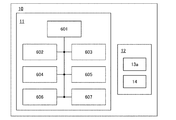
A specific configuration example of the
図13に示す半導体装置10は、集積回路11と、集積回路12とを有する。集積回路11は、制御装置601と、演算装置602と、メインメモリ603と、入力装置604と、出力装置605、IF(インターフェース)606と、緩衝記憶装置607とを有する。集積回路12は、回路13aと、記憶回路14とを有する。
A
制御装置601は、半導体装置10が有する演算装置602、メインメモリ603、入力装置604、出力装置605、IF606、緩衝記憶装置607の動作を統括的に制御することで、入力されたアプリケーションなどのプログラムに含まれる命令をデコードし、実行する機能を有する。演算装置602は、四則演算、論理演算などの各種演算処理を行う機能を有する。
The
なお、図13では、制御装置601と演算装置602とを独立したブロックとしてそれぞれ図示しているが、半導体装置10は、制御装置601の機能と、演算装置602の機能とを併せ持った中央演算処理装置を、制御装置601及び演算装置602の代わりに有していても良い。
In FIG. 13, the
メインメモリ603は、制御装置601において実行される、複数の命令で構成されるアプリケーションなどのプログラムと、演算装置602における演算処理に用いられるデータとを、記憶する機能を有する。
The
緩衝記憶装置607は、演算装置602の演算処理の途中で得られたデータ、或いは演算装置602の演算処理の結果得られたデータなどを記憶する機能を有する。また、アプリケーションなどのプログラムを一時的に記憶する機能を有していても良い。
The
入力装置604は、半導体装置の外部から入力される命令を、半導体装置10に送る機能を有する。入力装置604として、例えば、キーボード、マウス、タッチパネルなどを用いることができる。
The
出力装置605は、半導体装置10の動作状態、アプリケーションなどのプログラムの実行により得られた結果などを、情報として出力する機能を有する。出力装置605として、例えば、ディスプレイ、プロジェクタ、プリンタ、プロッター、音声出力装置などを用いることができる。
The
IF606は、集積回路11と集積回路12との間におけるデータの経路に相当する。具体的に、回路13aで生成されたテストパターンは、IF606を介して集積回路11に送られる。そして、テストパターンに従って集積回路11が動作することで得られた信号は、IF606を介して回路13aに送られる。また、記憶回路14が、緩衝記憶装置607と共にセット連想方式の緩衝記憶装置として機能する場合、記憶回路14は、緩衝記憶装置607と共に、演算装置602の演算処理の途中で得られたデータ、或いは演算装置602の演算処理の結果得られたデータなどを記憶する機能を有する。また、アプリケーションなどのプログラムを一時的に記憶する機能を有していても良い。
The
制御装置601において命令の実行が繰り返されることで、プログラムが実行される。
The program is executed by repeatedly executing the instruction in the
〈トランジスタについて〉
本発明の一態様に係る半導体装置では、図5または図8に示すトランジスタ41のオフ電流が小さいと、データの保持期間を長くすることができる。そのため、トランジスタ41として、酸化物半導体膜にチャネル形成領域を有するトランジスタを用いることが望ましい。
<About the transistor>
In the semiconductor device according to one embodiment of the present invention, the data retention period can be extended when the off-state current of the
図15に、酸化物半導体膜にチャネル形成領域を有するトランジスタ41の構成を、一例として示す。図15(A)には、トランジスタ41の上面図を示す。なお、図15(A)では、トランジスタ41のレイアウトを明確にするために、各種の絶縁膜を省略している。また、図15(A)に示した上面図の、破線A1−A2における断面図を図15(B)に示し、破線A3−A4における断面図を図15(C)に示す。
FIG. 15 illustrates an example of a structure of the
図15に示すように、トランジスタ41は、絶縁膜81上において順に積層された酸化物半導体膜82a及び酸化物半導体膜82bと、酸化物半導体膜82bに電気的に接続され、ソース電極またはドレイン電極としての機能を有する導電膜83及び導電膜84と、酸化物半導体膜82b、導電膜83及び導電膜84上の酸化物半導体膜82cと、ゲート絶縁膜としての機能を有し、なおかつ酸化物半導体膜82c上に位置する絶縁膜85と、ゲート電極としての機能を有し、なおかつ絶縁膜85上において酸化物半導体膜82a乃至酸化物半導体膜82cと重なる導電膜86とを有する。
As illustrated in FIG. 15, the
また、トランジスタ41の、具体的な構成の別の一例を、図16に示す。図16(A)には、トランジスタ41の上面図を示す。なお、図16(A)では、トランジスタ41のレイアウトを明確にするために、各種の絶縁膜を省略している。また、図16(A)に示した上面図の、破線A1−A2における断面図を図16(B)に示し、破線A3−A4における断面図を図16(C)に示す。
Further, another example of a specific structure of the
図16に示すように、トランジスタ41は、絶縁膜81上において順に積層された酸化物半導体膜82a乃至酸化物半導体膜82cと、酸化物半導体膜82cに電気的に接続され、ソース電極またはドレイン電極としての機能を有する導電膜83及び導電膜84と、ゲート絶縁膜としての機能を有し、なおかつ酸化物半導体膜82c、導電膜83及び導電膜84上に位置する絶縁膜85と、ゲート電極としての機能を有し、なおかつ絶縁膜85上において酸化物半導体膜82a乃至酸化物半導体膜82cと重なる導電膜86とを有する。
As illustrated in FIG. 16, the
なお、図15及び図16では、積層された酸化物半導体膜82a乃至酸化物半導体膜82cを用いるトランジスタ41の構成を例示している。トランジスタ41が有する酸化物半導体膜は、積層された複数の酸化物半導体膜で構成されているとは限らず、単膜の酸化物半導体膜で構成されていても良い。
Note that FIGS. 15 and 16 illustrate the structure of the
酸化物半導体膜82a乃至酸化物半導体膜82cが順に積層されている半導体膜をトランジスタ41が有する場合、酸化物半導体膜82a及び酸化物半導体膜82cは、酸化物半導体膜82bを構成する金属元素の少なくとも1つを、その構成要素に含み、伝導帯下端のエネルギーが酸化物半導体膜82bよりも0.05eV以上、0.07eV以上、0.1eV以上または0.15eV以上、かつ2eV以下、1eV以下、0.5eV以下または0.4eV以下、真空準位に近い酸化物膜である。さらに、酸化物半導体膜82bは、少なくともインジウムを含むと、キャリア移動度が高くなるため好ましい。
In the case where the
上記構成の半導体膜をトランジスタ41が有する場合、ゲート電極に電圧を印加することで、半導体膜に電界が加わると、半導体膜のうち、伝導帯下端のエネルギーが小さい酸化物半導体膜82bにチャネル領域が形成される。即ち、酸化物半導体膜82bと絶縁膜85との間に酸化物半導体膜82cが設けられていることによって、絶縁膜85と離隔している酸化物半導体膜82bに、チャネル領域を形成することができる。
In the case where the
また、酸化物半導体膜82cは、酸化物半導体膜82bを構成する金属元素の少なくとも1つをその構成要素に含むため、酸化物半導体膜82bと酸化物半導体膜82cの界面では、界面散乱が起こりにくい。従って、当該界面においてキャリアの動きが阻害されにくいため、トランジスタ41の電界効果移動度が高くなる。
In addition, since the
また、酸化物半導体膜82bと酸化物半導体膜82aの界面に界面準位が形成されると、界面近傍の領域にもチャネル領域が形成されるために、トランジスタ41の閾値電圧が変動してしまう。しかし、酸化物半導体膜82aは、酸化物半導体膜82bを構成する金属元素の少なくとも1つをその構成要素に含むため、酸化物半導体膜82bと酸化物半導体膜82aの界面には、界面準位が形成されにくい。よって、上記構成により、トランジスタ41の閾値電圧等の電気的特性のばらつきを、低減することができる。
In addition, when an interface state is formed at the interface between the
また、酸化物半導体膜間に不純物が存在することによって、各膜の界面にキャリアの流れを阻害する界面準位が形成されることがないよう、複数の酸化物半導体膜を積層させることが望ましい。積層された酸化物半導体膜の膜間に不純物が存在していると、酸化物半導体膜間における伝導帯下端のエネルギーの連続性が失われ、界面近傍において、キャリアがトラップされるか、あるいは再結合により消滅してしまうからである。膜間における不純物を低減させることで、主成分である一の金属を少なくとも共に有する複数の酸化物半導体膜を、単に積層させるよりも、連続接合(ここでは特に伝導帯下端のエネルギーが各膜の間で連続的に変化するU字型の井戸構造を有している状態)が形成されやすくなる。 In addition, it is preferable to stack a plurality of oxide semiconductor films so that an interface state that inhibits the flow of carriers is not formed at the interface of each film due to the presence of impurities between the oxide semiconductor films. . If impurities exist between the stacked oxide semiconductor films, the continuity of the energy at the bottom of the conduction band between the oxide semiconductor films is lost, and carriers are trapped or re-entered near the interface. This is because the bonds disappear. By reducing the impurities between the films, a plurality of oxide semiconductor films having at least one metal as a main component together are simply stacked rather than simply stacked (here, the energy at the lower end of the conduction band is particularly high in each film). A state of having a U-shaped well structure that continuously changes between them).
連続接合を形成するためには、ロードロック室を備えたマルチチャンバー方式の成膜装置(スパッタリング装置)を用いて各膜を大気に触れさせることなく連続して積層することが必要となる。スパッタリング装置における各チャンバーは、酸化物半導体にとって不純物となる水等を可能な限り除去すべくクライオポンプのような吸着式の真空排気ポンプを用いて高真空排気(5×10⁻⁷Pa以上1×10⁻⁴Pa以下程度)することが好ましい。または、ターボ分子ポンプとコールドトラップを組み合わせて排気系からチャンバー内に気体が逆流しないようにしておくことが好ましい。 In order to form a continuous bond, it is necessary to use a multi-chamber type film forming apparatus (sputtering apparatus) provided with a load lock chamber to continuously laminate each film without exposure to the atmosphere. Each chamber in the sputtering apparatus is subjected to high vacuum exhaustion (5 × 10 −7 Pa or more 1 ×) using an adsorption-type vacuum exhaust pump such as a cryopump to remove as much as possible water which is an impurity for the oxide semiconductor. 10 −4 Pa or less). Alternatively, it is preferable to combine a turbo molecular pump and a cold trap so that gas does not flow backward from the exhaust system into the chamber.
高純度の真性な酸化物半導体を得るためには、各チャンバー内を高真空排気するのみならず、スパッタリングに用いるガスの高純度化も重要である。上記ガスとして用いる酸素ガスやアルゴンガスの露点を、−40℃以下、好ましくは−80℃以下、より好ましくは−100℃以下とし、使用するガスの高純度化を図ることで、酸化物半導体膜に水分等が取り込まれることを可能な限り防ぐことができる。具体的に、酸化物半導体膜82bがIn−M−Zn酸化物(Mは、Ga、Y、Zr、La、Ce、またはNd)の場合、酸化物半導体膜82bを成膜するために用いるターゲットにおいて、金属元素の原子数比をIn:M:Zn=x1:y1:z1とすると、x1/y1は、1/3以上6以下、さらには1以上6以下であって、z1/y1は、1/3以上6以下、さらには1以上6以下であることが好ましい。なお、z1/y1を1以上6以下とすることで、酸化物半導体膜82bとしてCAAC−OS(C Axis Aligned Crystalline Oxide Semiconductor)膜が形成されやすくなる。ターゲットの金属元素の原子数比の代表例としては、In:M:Zn=1:1:1、In:M:Zn=3:1:2等がある。
In order to obtain a high-purity intrinsic oxide semiconductor, it is important not only to evacuate each chamber to a high vacuum but also to increase the purity of a gas used for sputtering. The dew point of oxygen gas or argon gas used as the gas is −40 ° C. or lower, preferably −80 ° C. or lower, more preferably −100 ° C. or lower, and the oxide semiconductor film is made highly purified by purifying the gas used. It is possible to prevent moisture and the like from being taken into the body as much as possible. Specifically, when the
具体的に、酸化物半導体膜82a、酸化物半導体膜82cがIn−M−Zn酸化物(Mは、Ga、Y、Zr、La、Ce、またはNd)の場合、酸化物半導体膜82a、酸化物半導体膜82cを成膜するために用いるターゲットにおいて、金属元素の原子数比をIn:M:Zn=x2:y2:z2とすると、x2/y2<x1/y1であって、z2/y2は、1/3以上6以下、さらには1以上6以下であることが好ましい。なお、z2/y2を1以上6以下とすることで、酸化物半導体膜82a、酸化物半導体膜82cとしてCAAC−OS膜が形成されやすくなる。ターゲットの金属元素の原子数比の代表例としては、In:M:Zn=1:3:2、In:M:Zn=1:3:4、In:M:Zn=1:3:6、In:M:Zn=1:3:8等がある。
Specifically, in the case where the
なお、酸化物半導体膜82a及び酸化物半導体膜82cの厚さは、3nm以上100nm以下、好ましくは3nm以上50nm以下とする。また、酸化物半導体膜82bの厚さは、3nm以上200nm以下、好ましくは3nm以上100nm以下であり、さらに好ましくは3nm以上50nm以下である。
Note that the thickness of the
3層構造の半導体膜において、酸化物半導体膜82a乃至酸化物半導体膜82cは、非晶質または結晶質の両方の形態を取りうる。ただし、チャネル領域が形成される酸化物半導体膜82bが結晶質であることにより、トランジスタ41に安定した電気的特性を付与することができるため、酸化物半導体膜82bは結晶質であることが好ましい。
In the three-layer semiconductor film, the
なお、チャネル形成領域とは、トランジスタ41の半導体膜のうち、ゲート電極と重なり、かつソース電極とドレイン電極に挟まれる領域を意味する。また、チャネル領域とは、チャネル形成領域において、電流が主として流れる領域をいう。
Note that the channel formation region means a region of the semiconductor film of the
例えば、酸化物半導体膜82a及び酸化物半導体膜82cとして、スパッタリング法により形成したIn−Ga−Zn酸化物膜を用いる場合、酸化物半導体膜82a及び酸化物半導体膜82cの成膜には、In−Ga−Zn酸化物(In:Ga:Zn=1:3:2[原子数比])であるターゲットを用いることができる。成膜条件は、例えば、成膜ガスとしてアルゴンガスを30sccm、酸素ガスを15sccm用い、圧力0.4Paとし、基板温度を200℃とし、DC電力0.5kWとすればよい。
For example, in the case where an In—Ga—Zn oxide film formed by a sputtering method is used as the
また、酸化物半導体膜82bをCAAC−OS膜とする場合、酸化物半導体膜82bの成膜には、In−Ga−Zn酸化物(In:Ga:Zn=1:1:1[原子数比])であり、In−Ga−Zn酸化物を含む多結晶ターゲットを用いることが好ましい。成膜条件は、例えば、成膜ガスとしてアルゴンガスを30sccm、酸素ガスを15sccm用い、圧力を0.4Paとし、基板の温度300℃とし、DC電力0.5kWとすることができる。
In the case where the
なお、酸化物半導体膜82a乃至82cは、スパッタリング法により形成することができるが、他の方法、例えば、熱CVD法により形成してもよい。熱CVD法の例としてMOCVD(Metal Organic Chemical Vapor Deposition)法やALD(Atomic Layer Deposition)法を使っても良い。
Note that the
なお、電子供与体(ドナー)となる水分または水素などの不純物が低減され、なおかつ酸素欠損が低減されることにより高純度化された酸化物半導体(purified Oxide Semiconductor)は、キャリア発生源が少ないため、i型(真性半導体)又はi型に限りなく近くすることができる。そのため、高純度化された酸化物半導体膜にチャネル形成領域を有するトランジスタは、オフ電流が著しく小さく、信頼性が高い。そして、当該酸化物半導体膜にチャネル形成領域が形成されるトランジスタは、閾値電圧がプラスとなる電気的特性(ノーマリーオフ特性ともいう。)になりやすい。 Note that an oxide semiconductor purified by reduction of impurities such as moisture or hydrogen which serves as an electron donor (donor) and oxygen vacancies are reduced because there are few carrier generation sources. , I-type (intrinsic semiconductor) or i-type. Therefore, a transistor including a channel formation region in a highly purified oxide semiconductor film has extremely low off-state current and high reliability. A transistor in which a channel formation region is formed in the oxide semiconductor film tends to have electrical characteristics (also referred to as normally-off characteristics) in which the threshold voltage is positive.
具体的に、高純度化された酸化物半導体膜にチャネル形成領域を有するトランジスタのオフ電流が小さいことは、いろいろな実験により証明できる。例えば、チャネル幅が1×106μmでチャネル長が10μmの素子であっても、ソース電極とドレイン電極間の電圧(ドレイン電圧)が1Vから10Vの範囲において、オフ電流が、半導体パラメータアナライザの測定限界以下、すなわち1×10⁻¹³A以下という特性を得ることができる。この場合、トランジスタのチャネル幅で規格化したオフ電流は、100zA/μm以下であることが分かる。また、容量素子とトランジスタとを接続して、容量素子に流入または容量素子から流出する電荷を当該トランジスタで制御する回路を用いて、オフ電流の測定を行った。当該測定では、高純度化された酸化物半導体膜を上記トランジスタのチャネル形成領域に用い、容量素子の単位時間あたりの電荷量の推移から当該トランジスタのオフ電流を測定した。その結果、トランジスタのソース電極とドレイン電極間の電圧が3Vの場合に、数十yA/μmという、さらに小さいオフ電流が得られることが分かった。従って、高純度化された酸化物半導体膜をチャネル形成領域に用いたトランジスタは、オフ電流が、結晶性を有するシリコンを用いたトランジスタに比べて著しく小さい。 Specifically, it can be proved by various experiments that the off-state current of a transistor including a channel formation region in a highly purified oxide semiconductor film is small. For example, even in an element having a channel width of 1 × 10 6 μm and a channel length of 10 μm, when the voltage between the source electrode and the drain electrode (drain voltage) is in the range of 1V to 10V, It is possible to obtain characteristics that are below the measurement limit, that is, 1 × 10 −13 A or less. In this case, it can be seen that the off-current normalized by the channel width of the transistor is 100 zA / μm or less. In addition, off-state current was measured using a circuit in which a capacitor and a transistor were connected and charge flowing into or out of the capacitor was controlled by the transistor. In this measurement, a highly purified oxide semiconductor film was used for a channel formation region of the transistor, and the off-state current of the transistor was measured from the change in charge amount per unit time of the capacitor. As a result, it was found that when the voltage between the source electrode and the drain electrode of the transistor is 3 V, an even smaller off current of several tens of yA / μm can be obtained. Therefore, a transistor using a highly purified oxide semiconductor film for a channel formation region has significantly lower off-state current than a transistor using crystalline silicon.
なお、半導体膜として酸化物半導体膜を用いる場合、酸化物半導体としては、少なくともインジウム(In)あるいは亜鉛(Zn)を含むことが好ましい。また、該酸化物半導体を用いたトランジスタの電気的特性のばらつきを減らすためのスタビライザーとして、それらに加えてガリウム(Ga)を有することが好ましい。また、スタビライザーとしてスズ(Sn)を有することが好ましい。また、スタビライザーとしてハフニウム(Hf)を有することが好ましい。また、スタビライザーとしてアルミニウム(Al)を有することが好ましい。また、スタビライザーとしてジルコニウム(Zr)を含むことが好ましい。 Note that in the case where an oxide semiconductor film is used as the semiconductor film, the oxide semiconductor preferably contains at least indium (In) or zinc (Zn). In addition, it is preferable that gallium (Ga) be included in addition to the stabilizer for reducing variation in electrical characteristics of the transistor including the oxide semiconductor. Moreover, it is preferable to have tin (Sn) as a stabilizer. Moreover, it is preferable to have hafnium (Hf) as a stabilizer. Moreover, it is preferable to have aluminum (Al) as a stabilizer. Moreover, it is preferable that zirconium (Zr) is included as a stabilizer.
酸化物半導体の中でもIn−Ga−Zn酸化物、In−Sn−Zn酸化物などは、炭化シリコン、窒化ガリウム、または酸化ガリウムとは異なり、スパッタリング法や湿式法により電気的特性の優れたトランジスタを作製することが可能であり、量産性に優れるといった利点がある。また、炭化シリコン、窒化ガリウム、または酸化ガリウムとは異なり、上記In−Ga−Zn酸化物は、ガラス基板上に、電気的特性の優れたトランジスタを作製することが可能である。また、基板の大型化にも対応が可能である。 Among oxide semiconductors, In-Ga-Zn oxide, In-Sn-Zn oxide, and the like are different from silicon carbide, gallium nitride, or gallium oxide, transistors having excellent electrical characteristics can be formed by a sputtering method or a wet method. There is an advantage that it can be manufactured and is excellent in mass productivity. Further, unlike silicon carbide, gallium nitride, or gallium oxide, the In—Ga—Zn oxide can form a transistor with excellent electrical characteristics over a glass substrate. In addition, it is possible to cope with an increase in the size of the substrate.
また、他のスタビライザーとして、ランタノイドである、ランタン(La)、セリウム(Ce)、プラセオジム(Pr)、ネオジム(Nd)、サマリウム(Sm)、ユウロピウム(Eu)、ガドリニウム(Gd)、テルビウム(Tb)、ジスプロシウム(Dy)、ホルミウム(Ho)、エルビウム(Er)、ツリウム(Tm)、イッテルビウム(Yb)、ルテチウム(Lu)のいずれか一種または複数種を含んでいてもよい。 As other stabilizers, lanthanoids such as lanthanum (La), cerium (Ce), praseodymium (Pr), neodymium (Nd), samarium (Sm), europium (Eu), gadolinium (Gd), terbium (Tb) , Dysprosium (Dy), holmium (Ho), erbium (Er), thulium (Tm), ytterbium (Yb), or lutetium (Lu) may be included.
例えば、酸化物半導体として、酸化インジウム、酸化ガリウム、酸化スズ、酸化亜鉛、In−Zn酸化物、Sn−Zn酸化物、Al−Zn酸化物、Zn−Mg酸化物、Sn−Mg酸化物、In−Mg酸化物、In−Ga酸化物、In−Ga−Zn酸化物(IGZOとも表記する)、In−Al−Zn酸化物、In−Sn−Zn酸化物、Sn−Ga−Zn酸化物、Al−Ga−Zn酸化物、Sn−Al−Zn酸化物、In−Hf−Zn酸化物、In−La−Zn酸化物、In−Pr−Zn酸化物、In−Nd−Zn酸化物、In−Ce−Zn酸化物、In−Sm−Zn酸化物、In−Eu−Zn酸化物、In−Gd−Zn酸化物、In−Tb−Zn酸化物、In−Dy−Zn酸化物、In−Ho−Zn酸化物、In−Er−Zn酸化物、In−Tm−Zn酸化物、In−Yb−Zn酸化物、In−Lu−Zn酸化物、In−Sn−Ga−Zn酸化物、In−Hf−Ga−Zn酸化物、In−Al−Ga−Zn酸化物、In−Sn−Al−Zn酸化物、In−Sn−Hf−Zn酸化物、In−Hf−Al−Zn酸化物を用いることができる。 For example, as an oxide semiconductor, indium oxide, gallium oxide, tin oxide, zinc oxide, In-Zn oxide, Sn-Zn oxide, Al-Zn oxide, Zn-Mg oxide, Sn-Mg oxide, In -Mg oxide, In-Ga oxide, In-Ga-Zn oxide (also expressed as IGZO), In-Al-Zn oxide, In-Sn-Zn oxide, Sn-Ga-Zn oxide, Al -Ga-Zn oxide, Sn-Al-Zn oxide, In-Hf-Zn oxide, In-La-Zn oxide, In-Pr-Zn oxide, In-Nd-Zn oxide, In-Ce -Zn oxide, In-Sm-Zn oxide, In-Eu-Zn oxide, In-Gd-Zn oxide, In-Tb-Zn oxide, In-Dy-Zn oxide, In-Ho-Zn Oxide, In-Er-Zn oxide, In- m-Zn oxide, In-Yb-Zn oxide, In-Lu-Zn oxide, In-Sn-Ga-Zn oxide, In-Hf-Ga-Zn oxide, In-Al-Ga-Zn oxide In-Sn-Al-Zn oxide, In-Sn-Hf-Zn oxide, and In-Hf-Al-Zn oxide can be used.
なお、例えば、In−Ga−Zn酸化物とは、InとGaとZnを含む酸化物という意味であり、InとGaとZnの比率は問わない。また、InとGaとZn以外の金属元素を含んでいてもよい。In−Ga−Zn酸化物は、無電界時の抵抗が十分に高くオフ電流を十分に小さくすることが可能であり、また、移動度も高い。 Note that for example, an In—Ga—Zn oxide means an oxide containing In, Ga, and Zn, and there is no limitation on the ratio of In, Ga, and Zn. Moreover, metal elements other than In, Ga, and Zn may be included. An In—Ga—Zn oxide has sufficiently high resistance in the absence of an electric field and can have a sufficiently small off-state current, and has high mobility.
例えば、In−Sn−Zn酸化物では比較的容易に高い移動度が得られる。しかしながら、In−Ga−Zn酸化物でも、バルク内欠陥密度を低減することにより移動度を上げることができる。 For example, high mobility can be obtained relatively easily with an In—Sn—Zn oxide. However, mobility can be increased by reducing the defect density in the bulk also in the case of using the In—Ga—Zn oxide.
また、トランジスタ41において、ソース電極及びドレイン電極に用いられる導電性材料によっては、ソース電極及びドレイン電極中の金属が、酸化物半導体膜から酸素を引き抜くことがある。この場合、酸化物半導体膜のうち、ソース電極及びドレイン電極に接する領域が、酸素欠損の形成によりn型化される。n型化された領域は、ソース領域またはドレイン領域として機能するため、酸化物半導体膜とソース電極及びドレイン電極との間におけるコンタクト抵抗を下げることができる。よって、n型化された領域が形成されることで、トランジスタ41の移動度及びオン電流を高めることができ、それにより、トランジスタ41を用いた半導体装置の高速動作を実現することができる。
In the
なお、ソース電極及びドレイン電極中の金属による酸素の引き抜きは、ソース電極及びドレイン電極をスパッタリング法などにより形成する際に起こりうるし、ソース電極及びドレイン電極を形成した後に行われる加熱処理によっても起こりうる。また、n型化される領域は、酸素と結合し易い導電性材料をソース電極及びドレイン電極に用いることで、より形成されやすくなる。上記導電性材料としては、例えば、Al、Cr、Cu、Ta、Ti、Mo、Wなどが挙げられる。 Note that extraction of oxygen by a metal in the source electrode and the drain electrode can occur when the source electrode and the drain electrode are formed by a sputtering method or the like, and can also occur by a heat treatment performed after the source electrode and the drain electrode are formed. . In addition, the n-type region is more easily formed by using a conductive material that is easily bonded to oxygen for the source electrode and the drain electrode. Examples of the conductive material include Al, Cr, Cu, Ta, Ti, Mo, and W.
複数の積層された酸化物半導体膜を有する半導体膜をトランジスタ41に用いる場合、n型化される領域は、チャネル領域となる酸化物半導体膜82bにまで達していることが、トランジスタ41の移動度及びオン電流を高め、半導体装置の高速動作を実現する上で好ましい。
In the case where a semiconductor film including a plurality of stacked oxide semiconductor films is used for the
絶縁膜81は、加熱により酸素を酸化物半導体膜82a乃至酸化物半導体膜82cに供給する機能を有する絶縁膜であることが望ましい。また、絶縁膜81は、欠陥が少ないことが好ましく、代表的には、ESR測定により得られる、シリコンのダングリングボンドに由来するg=2.001を持つスピンの密度が1×10¹⁸spins/cm3以下であることが好ましい。
The insulating
絶縁膜81は、加熱により酸素を酸化物半導体膜82a乃至酸化物半導体膜82cに供給する機能を有するため、酸化物であることが望ましく、例えば、酸化アルミニウム、酸化マグネシウム、酸化珪素、酸化窒化珪素、窒化酸化珪素、酸化ガリウム、酸化ゲルマニウム、酸化イットリウム、酸化ジルコニウム、酸化ランタン、酸化ネオジム、酸化ハフニウムおよび酸化タンタルなどを用いることができる。絶縁膜81は、プラズマCVD(Chemical Vapor Deposition)法またはスパッタリング法等により、形成することができる。
The insulating
なお、本明細書中において、酸化窒化物は、その組成として、窒素よりも酸素の含有量が多い材料を指し、窒化酸化物は、その組成として、酸素よりも窒素の含有量が多い材料を指す。 Note that in this specification, oxynitride refers to a material having a higher oxygen content than nitrogen as its composition, and nitride oxide refers to a material having a higher nitrogen content than oxygen as its composition. Point to.
なお、図15及び図16に示すトランジスタ41は、チャネル領域が形成される酸化物半導体膜82bの端部のうち、導電膜83及び導電膜84とは重ならない端部、言い換えると、導電膜83及び導電膜84が位置する領域とは異なる領域に位置する端部と、導電膜86とが、重なる構成を有する。酸化物半導体膜82bの端部は、当該端部を形成するためのエッチングでプラズマに曝されるときに、エッチングガスから生じた塩素ラジカル、フッ素ラジカル等が、酸化物半導体を構成する金属元素と結合しやすい。よって、酸化物半導体膜の端部では、当該金属元素と結合していた酸素が脱離しやすい状態にあるため、酸素欠損が形成され、n型化しやすいやすい。しかし、図15及び図16に示すトランジスタ41では、導電膜83及び導電膜84とは重ならない酸化物半導体膜82bの端部と、導電膜86とが重なるため、導電膜86の電位を制御することにより、当該端部にかかる電界を制御することができる。よって、酸化物半導体膜82bの端部を介して導電膜83と導電膜84の間に流れる電流を、導電膜86に与える電位によって制御することができる。このようなトランジスタ41の構造を、Surrounded Channel(S−Channel)構造とよぶ。
Note that the
具体的に、S−Channel構造の場合、トランジスタ41がオフとなるような電位を導電膜86に与えたときは、当該端部を介して導電膜83と導電膜84の間に流れるオフ電流を小さく抑えることができる。そのため、トランジスタ41では、大きなオン電流を得るためにチャネル長を短くし、その結果、酸化物半導体膜82bの端部における導電膜83と導電膜84の間の長さが短くなっても、トランジスタ41のオフ電流を小さく抑えることができる。よって、トランジスタ41は、チャネル長を短くすることで、オンのときには大きいオン電流を得ることができ、オフのときにはオフ電流を小さく抑えることができる。
Specifically, in the case of the S-Channel structure, when a potential at which the
また、具体的に、S−Channel構造の場合、トランジスタ41がオンとなるような電位を導電膜86に与えたときは、当該端部を介して導電膜83と導電膜84の間に流れる電流を大きくすることができる。当該電流は、トランジスタ41の電界効果移動度とオン電流の増大に寄与する。そして、酸化物半導体膜82bの端部と、導電膜86とが重なることで、酸化物半導体膜82bにおいてキャリアの流れる領域が、絶縁膜85に近い酸化物半導体膜82bの界面近傍のみでなく、酸化物半導体膜82bの広い範囲においてキャリアが流れるため、トランジスタ41におけるキャリアの移動量が増加する。この結果、トランジスタ41のオン電流が大きくなる共に、電界効果移動度が高くなり、代表的には電界効果移動度が10cm2/V・s以上、さらには20cm2/V・s以上となる。なお、ここでの電界効果移動度は、酸化物半導体膜の物性値としての移動度の近似値ではなく、トランジスタの飽和領域における電流駆動力の指標であり、見かけ上の電界効果移動度である。
Specifically, in the case of the S-Channel structure, when a potential at which the
以下では、酸化物半導体膜の構造について説明する。 Hereinafter, the structure of the oxide semiconductor film is described.
なお、本明細書において、「平行」とは、二つの直線が−10°以上10°以下の角度で配置されている状態をいう。したがって、−5°以上5°以下の場合も含まれる。また、「略平行」とは、二つの直線が−30°以上30°以下の角度で配置されている状態をいう。また、「垂直」とは、二つの直線が80°以上100°以下の角度で配置されている状態をいう。したがって、85°以上95°以下の場合も含まれる。また、「略垂直」とは、二つの直線が60°以上120°以下の角度で配置されている状態をいう。また、本明細書において、結晶が三方晶または菱面体晶である場合、六方晶系として表す。 In this specification, “parallel” refers to a state in which two straight lines are arranged at an angle of −10 ° to 10 °. Therefore, the case of −5 ° to 5 ° is also included. Further, “substantially parallel” means a state in which two straight lines are arranged at an angle of −30 ° to 30 °. “Vertical” refers to a state in which two straight lines are arranged at an angle of 80 ° to 100 °. Therefore, the case of 85 ° to 95 ° is also included. Further, “substantially vertical” means a state in which two straight lines are arranged at an angle of 60 ° to 120 °. In this specification, when a crystal is trigonal or rhombohedral, it is represented as a hexagonal system.
酸化物半導体膜は、非単結晶酸化物半導体膜と単結晶酸化物半導体膜とに分けられる。または、酸化物半導体は、例えば、結晶性酸化物半導体と非晶質酸化物半導体とに分けられる。 An oxide semiconductor film is classified into a non-single-crystal oxide semiconductor film and a single-crystal oxide semiconductor film. Alternatively, an oxide semiconductor is classified into, for example, a crystalline oxide semiconductor and an amorphous oxide semiconductor.
なお、非単結晶酸化物半導体としては、CAAC−OS、多結晶酸化物半導体、微結晶酸化物半導体、非晶質酸化物半導体などがある。また、結晶性酸化物半導体としては、単結晶酸化物半導体、CAAC−OS、多結晶酸化物半導体、微結晶酸化物半導体などがある。 Note that as the non-single-crystal oxide semiconductor, a CAAC-OS, a polycrystalline oxide semiconductor, a microcrystalline oxide semiconductor, an amorphous oxide semiconductor, or the like can be given. As a crystalline oxide semiconductor, a single crystal oxide semiconductor, a CAAC-OS, a polycrystalline oxide semiconductor, a microcrystalline oxide semiconductor, or the like can be given.
まずは、CAAC−OS膜について説明する。 First, the CAAC-OS film is described.
CAAC−OS膜は、c軸配向した複数の結晶部を有する酸化物半導体膜の一つである。 The CAAC-OS film is one of oxide semiconductor films having a plurality of c-axis aligned crystal parts.
透過型電子顕微鏡(TEM:Transmission Electron Microscope)によって、CAAC−OS膜の明視野像および回折パターンの複合解析像(高分解能TEM像ともいう。)を観察することで複数の結晶部を確認することができる。一方、高分解能TEM像によっても明確な結晶部同士の境界、即ち結晶粒界(グレインバウンダリーともいう。)を確認することができない。そのため、CAAC−OS膜は、結晶粒界に起因する電子移動度の低下が起こりにくいといえる。 Confirming a plurality of crystal parts by observing a bright field image of a CAAC-OS film and a combined analysis image (also referred to as a high-resolution TEM image) of a CAAC-OS film with a transmission electron microscope (TEM: Transmission Electron Microscope). Can do. On the other hand, a clear boundary between crystal parts, that is, a crystal grain boundary (also referred to as a grain boundary) cannot be confirmed even by a high-resolution TEM image. Therefore, it can be said that the CAAC-OS film is unlikely to decrease in electron mobility due to crystal grain boundaries.
試料面と略平行な方向から、CAAC−OS膜の断面の高分解能TEM像を観察すると、結晶部において、金属原子が層状に配列していることを確認できる。金属原子の各層は、CAAC−OS膜の膜を形成する面(被形成面ともいう。)または上面の凹凸を反映した形状であり、CAAC−OS膜の被形成面または上面と平行に配列する。 When a high-resolution TEM image of a cross section of the CAAC-OS film is observed from a direction substantially parallel to the sample surface, it can be confirmed that metal atoms are arranged in layers in the crystal part. Each layer of metal atoms has a shape reflecting unevenness of a surface (also referred to as a formation surface) or an upper surface on which the CAAC-OS film is formed, and is arranged in parallel with the formation surface or the upper surface of the CAAC-OS film. .
一方、試料面と略垂直な方向から、CAAC−OS膜の平面の高分解能TEM像を観察すると、結晶部において、金属原子が三角形状または六角形状に配列していることを確認できる。しかしながら、異なる結晶部間で、金属原子の配列に規則性は見られない。 On the other hand, when a high-resolution TEM image of a plane of the CAAC-OS film is observed from a direction substantially perpendicular to the sample surface, it can be confirmed that metal atoms are arranged in a triangular shape or a hexagonal shape in a crystal part. However, there is no regularity in the arrangement of metal atoms between different crystal parts.
CAAC−OS膜に対し、X線回折(XRD:X−Ray Diffraction)装置を用いて構造解析を行うと、例えばInGaZnO4の結晶を有するCAAC−OS膜のout−of−plane法による解析では、回折角(2θ)が31°近傍にピークが現れる場合がある。このピークは、InGaZnO4の結晶の(009)面に帰属されることから、CAAC−OS膜の結晶がc軸配向性を有し、c軸が被形成面または上面に略垂直な方向を向いていることが確認できる。 When structural analysis is performed on a CAAC-OS film using an X-ray diffraction (XRD) apparatus, for example, in the analysis of a CAAC-OS film having an InGaZnO 4 crystal by an out-of-plane method, A peak may appear when the diffraction angle (2θ) is around 31 °. Since this peak is attributed to the (009) plane of the InGaZnO 4 crystal, the crystal of the CAAC-OS film has c-axis orientation, and the c-axis is oriented in a direction substantially perpendicular to the formation surface or the top surface. Can be confirmed.
なお、InGaZnO4の結晶を有するCAAC−OS膜のout−of−plane法による解析では、2θが31°近傍のピークの他に、2θが36°近傍にもピークが現れる場合がある。2θが36°近傍のピークは、CAAC−OS膜中の一部に、c軸配向性を有さない結晶が含まれることを示している。CAAC−OS膜は、2θが31°近傍にピークを示し、2θが36°近傍にピークを示さないことが好ましい。 Note that when the CAAC-OS film including an InGaZnO 4 crystal is analyzed by an out-of-plane method, a peak may also appear when 2θ is around 36 ° in addition to the peak where 2θ is around 31 °. A peak at 2θ of around 36 ° indicates that a crystal having no c-axis alignment is included in part of the CAAC-OS film. The CAAC-OS film preferably has a peak at 2θ of around 31 ° and no peak at 2θ of around 36 °.
CAAC−OS膜は、不純物濃度の低い酸化物半導体膜である。不純物は、水素、炭素、シリコン、遷移金属元素などの酸化物半導体膜の主成分以外の元素である。特に、シリコンなどの、酸化物半導体膜を構成する金属元素よりも酸素との結合力の強い元素は、酸化物半導体膜から酸素を奪うことで酸化物半導体膜の原子配列を乱し、結晶性を低下させる要因となる。また、鉄やニッケルなどの重金属、アルゴン、二酸化炭素などは、原子半径(または分子半径)が大きいため、酸化物半導体膜内部に含まれると、酸化物半導体膜の原子配列を乱し、結晶性を低下させる要因となる。なお、酸化物半導体膜に含まれる不純物は、キャリアトラップやキャリア発生源となる場合がある。 The CAAC-OS film is an oxide semiconductor film with a low impurity concentration. The impurity is an element other than the main component of the oxide semiconductor film, such as hydrogen, carbon, silicon, or a transition metal element. In particular, an element such as silicon, which has a stronger bonding force with oxygen than the metal element included in the oxide semiconductor film, disturbs the atomic arrangement of the oxide semiconductor film by depriving the oxide semiconductor film of oxygen, and has crystallinity. It becomes a factor to reduce. In addition, heavy metals such as iron and nickel, argon, carbon dioxide, and the like have large atomic radii (or molecular radii). Therefore, if they are contained inside an oxide semiconductor film, the atomic arrangement of the oxide semiconductor film is disturbed, resulting in crystallinity. It becomes a factor to reduce. Note that the impurity contained in the oxide semiconductor film might serve as a carrier trap or a carrier generation source.
また、CAAC−OS膜は、欠陥準位密度の低い酸化物半導体膜である。例えば、酸化物半導体膜中の酸素欠損は、キャリアトラップとなることや、水素を捕獲することによってキャリア発生源となることがある。 The CAAC-OS film is an oxide semiconductor film with a low density of defect states. For example, oxygen vacancies in the oxide semiconductor film can serve as carrier traps or can generate carriers by capturing hydrogen.
不純物濃度が低く、欠陥準位密度が低い(酸素欠損の少ない)ことを、高純度真性または実質的に高純度真性と呼ぶ。高純度真性または実質的に高純度真性である酸化物半導体膜は、キャリア発生源が少ないため、キャリア密度を低くすることができる。したがって、当該酸化物半導体膜を用いたトランジスタは、しきい値電圧がマイナスとなる電気特性(ノーマリーオンともいう。)になることが少ない。また、高純度真性または実質的に高純度真性である酸化物半導体膜は、キャリアトラップが少ない。そのため、当該酸化物半導体膜を用いたトランジスタは、電気特性の変動が小さく、信頼性の高いトランジスタとなる。なお、酸化物半導体膜のキャリアトラップに捕獲された電荷は、放出するまでに要する時間が長く、あたかも固定電荷のように振る舞うことがある。そのため、不純物濃度が高く、欠陥準位密度が高い酸化物半導体膜を用いたトランジスタは、電気特性が不安定となる場合がある。 A low impurity concentration and a low density of defect states (small number of oxygen vacancies) is called high purity intrinsic or substantially high purity intrinsic. A highly purified intrinsic or substantially highly purified intrinsic oxide semiconductor film has few carrier generation sources, and thus can have a low carrier density. Therefore, a transistor including the oxide semiconductor film is unlikely to have electrical characteristics (also referred to as normally-on) in which the threshold voltage is negative. A highly purified intrinsic or substantially highly purified intrinsic oxide semiconductor film has few carrier traps. Therefore, a transistor including the oxide semiconductor film has a small change in electrical characteristics and has high reliability. Note that the charge trapped in the carrier trap of the oxide semiconductor film takes a long time to be released, and may behave as if it were a fixed charge. Therefore, a transistor including an oxide semiconductor film with a high impurity concentration and a high density of defect states may have unstable electrical characteristics.
また、CAAC−OS膜を用いたトランジスタは、可視光や紫外光の照射による電気特性の変動が小さい。 In addition, a transistor including a CAAC-OS film has little variation in electrical characteristics due to irradiation with visible light or ultraviolet light.
次に、微結晶酸化物半導体膜について説明する。 Next, a microcrystalline oxide semiconductor film is described.
微結晶酸化物半導体膜は、高分解能TEM像において、結晶部を確認することのできる領域と、明確な結晶部を確認することのできない領域と、を有する。微結晶酸化物半導体膜に含まれる結晶部は、1nm以上100nm以下、または1nm以上10nm以下の大きさであることが多い。特に、1nm以上10nm以下、または1nm以上3nm以下の微結晶であるナノ結晶(nc:nanocrystal)を有する酸化物半導体膜を、nc−OS(nanocrystalline Oxide Semiconductor)膜と呼ぶ。また、nc−OS膜は、例えば、高分解能TEM像では、結晶粒界を明確に確認できない場合がある。 The microcrystalline oxide semiconductor film includes a region where a crystal part can be confirmed and a region where a clear crystal part cannot be confirmed in a high-resolution TEM image. In most cases, a crystal part included in the microcrystalline oxide semiconductor film has a size of 1 nm to 100 nm, or 1 nm to 10 nm. In particular, an oxide semiconductor film including a nanocrystal (nc) that is a microcrystal of 1 nm to 10 nm, or 1 nm to 3 nm is referred to as an nc-OS (nanocrystalline Oxide Semiconductor) film. In the nc-OS film, for example, a crystal grain boundary may not be clearly confirmed in a high-resolution TEM image.
nc−OS膜は、微小な領域(例えば、1nm以上10nm以下の領域、特に1nm以上3nm以下の領域)において原子配列に周期性を有する。また、nc−OS膜は、異なる結晶部間で結晶方位に規則性が見られない。そのため、膜全体で配向性が見られない。したがって、nc−OS膜は、分析方法によっては、非晶質酸化物半導体膜と区別が付かない場合がある。例えば、nc−OS膜に対し、結晶部よりも大きい径のX線を用いるXRD装置を用いて構造解析を行うと、out−of−plane法による解析では、結晶面を示すピークが検出されない。また、nc−OS膜に対し、結晶部よりも大きいプローブ径(例えば50nm以上)の電子線を用いる電子回折(制限視野電子回折ともいう。)を行うと、ハローパターンのような回折パターンが観測される。一方、nc−OS膜に対し、結晶部の大きさと近いか結晶部より小さいプローブ径の電子線を用いるナノビーム電子回折を行うと、スポットが観測される。また、nc−OS膜に対しナノビーム電子回折を行うと、円を描くように(リング状に)輝度の高い領域が観測される場合がある。また、nc−OS膜に対しナノビーム電子回折を行うと、リング状の領域内に複数のスポットが観測される場合がある。 The nc-OS film has periodicity in atomic arrangement in a very small region (eg, a region of 1 nm to 10 nm, particularly a region of 1 nm to 3 nm). In addition, the nc-OS film does not have regularity in crystal orientation between different crystal parts. Therefore, orientation is not seen in the whole film. Therefore, the nc-OS film may not be distinguished from an amorphous oxide semiconductor film depending on an analysis method. For example, when structural analysis is performed on the nc-OS film using an XRD apparatus using X-rays having a diameter larger than that of the crystal part, a peak indicating a crystal plane is not detected in the analysis by the out-of-plane method. Further, when electron diffraction (also referred to as limited-field electron diffraction) using an electron beam with a probe diameter (for example, 50 nm or more) larger than that of the crystal part is performed on the nc-OS film, a diffraction pattern such as a halo pattern is observed. Is done. On the other hand, when nanobeam electron diffraction is performed on the nc-OS film using an electron beam having a probe diameter that is close to or smaller than the size of the crystal part, spots are observed. In addition, when nanobeam electron diffraction is performed on the nc-OS film, a region with high luminance may be observed so as to draw a circle (in a ring shape). Further, when nanobeam electron diffraction is performed on the nc-OS film, a plurality of spots may be observed in the ring-shaped region.
nc−OS膜は、非晶質酸化物半導体膜よりも規則性の高い酸化物半導体膜である。そのため、nc−OS膜は、非晶質酸化物半導体膜よりも欠陥準位密度が低くなる。ただし、nc−OS膜は、異なる結晶部間で結晶方位に規則性が見られない。そのため、nc−OS膜は、CAAC−OS膜と比べて欠陥準位密度が高くなる。 The nc-OS film is an oxide semiconductor film that has higher regularity than an amorphous oxide semiconductor film. Therefore, the nc-OS film has a lower density of defect states than the amorphous oxide semiconductor film. Note that the nc-OS film does not have regularity in crystal orientation between different crystal parts. Therefore, the nc-OS film has a higher density of defect states than the CAAC-OS film.
次に、非晶質酸化物半導体膜について説明する。 Next, an amorphous oxide semiconductor film is described.
非晶質酸化物半導体膜は、膜中における原子配列が不規則であり、結晶部を有さない酸化物半導体膜である。石英のような無定形状態を有する酸化物半導体膜が一例である。 An amorphous oxide semiconductor film is an oxide semiconductor film having an irregular atomic arrangement in the film and having no crystal part. An oxide semiconductor film having an amorphous state such as quartz is an example.
非晶質酸化物半導体膜は、高分解能TEM像において結晶部を確認することができない。 In the amorphous oxide semiconductor film, a crystal part cannot be confirmed in a high-resolution TEM image.
非晶質酸化物半導体膜に対し、XRD装置を用いた構造解析を行うと、out−of−plane法による解析では、結晶面を示すピークが検出されない。また、非晶質酸化物半導体膜に対し、電子回折を行うと、ハローパターンが観測される。また、非晶質酸化物半導体膜に対し、ナノビーム電子回折を行うと、スポットが観測されず、ハローパターンが観測される。 When structural analysis using an XRD apparatus is performed on an amorphous oxide semiconductor film, a peak indicating a crystal plane is not detected by analysis using an out-of-plane method. Further, when electron diffraction is performed on the amorphous oxide semiconductor film, a halo pattern is observed. Further, when nanobeam electron diffraction is performed on an amorphous oxide semiconductor film, no spot is observed and a halo pattern is observed.
なお、酸化物半導体膜は、nc−OS膜と非晶質酸化物半導体膜との間の物性を示す構造を有する場合がある。そのような構造を有する酸化物半導体膜を、特に非晶質ライク酸化物半導体(a−like OS:amorphous−like Oxide Semiconductor)膜と呼ぶ。 Note that the oxide semiconductor film may have a structure having physical properties between the nc-OS film and the amorphous oxide semiconductor film. An oxide semiconductor film having such a structure is particularly referred to as an amorphous-like oxide semiconductor (a-like OS) film.
a−like OS膜は、高分解能TEM像において鬆(ボイドともいう。)が観察される場合がある。また、高分解能TEM像において、明確に結晶部を確認することのできる領域と、結晶部を確認することのできない領域と、を有する。a−like OS膜は、TEMによる観察程度の微量な電子照射によって、結晶化が起こり、結晶部の成長が見られる場合がある。一方、良質なnc−OS膜であれば、TEMによる観察程度の微量な電子照射による結晶化はほとんど見られない。 In the a-like OS film, a void (also referred to as a void) may be observed in a high-resolution TEM image. Moreover, in a high-resolution TEM image, it has the area | region which can confirm a crystal part clearly, and the area | region which cannot confirm a crystal part. In some cases, the a-like OS film is crystallized by a small amount of electron irradiation as observed by a TEM, and a crystal part is grown. On the other hand, in the case of a good-quality nc-OS film, crystallization due to a small amount of electron irradiation comparable to that observed by TEM is hardly observed.
なお、a−like OS膜およびnc−OS膜の結晶部の大きさの計測は、高分解能TEM像を用いて行うことができる。例えば、InGaZnO4の結晶は層状構造を有し、In−O層の間に、Ga−Zn−O層を2層有する。InGaZnO4の結晶の単位格子は、In−O層を3層有し、またGa−Zn−O層を6層有する、計9層がc軸方向に層状に重なった構造を有する。よって、これらの近接する層同士の間隔は、(009)面の格子面間隔(d値ともいう。)と同程度であり、結晶構造解析からその値は0.29nmと求められている。そのため、高分解能TEM像における格子縞に着目し、格子縞の間隔が0.28nm以上0.30nm以下である箇所においては、それぞれの格子縞がInGaZnO4の結晶のa−b面に対応する。 Note that the crystal part size of the a-like OS film and the nc-OS film can be measured using high-resolution TEM images. For example, a crystal of InGaZnO 4 has a layered structure, and two Ga—Zn—O layers are provided between In—O layers. The unit cell of InGaZnO 4 crystal has a structure in which a total of nine layers including three In—O layers and six Ga—Zn—O layers are stacked in the c-axis direction. Therefore, the distance between these adjacent layers is approximately the same as the lattice spacing (also referred to as d value) of the (009) plane, and the value is determined to be 0.29 nm from crystal structure analysis. Therefore, paying attention to the lattice fringes in the high-resolution TEM image, each lattice fringe corresponds to the ab plane of the InGaZnO 4 crystal in a portion where the interval between the lattice fringes is 0.28 nm or more and 0.30 nm or less.
また、酸化物半導体膜は、構造ごとに密度が異なる場合がある。例えば、ある酸化物半導体膜の組成がわかれば、該組成と同じ組成における単結晶の密度と比較することにより、その酸化物半導体膜の構造を推定することができる。例えば、単結晶の密度に対し、a−like OS膜の密度は78.6%以上92.3%未満となる。また、例えば、単結晶の密度に対し、nc−OS膜の密度およびCAAC−OS膜の密度は92.3%以上100%未満となる。なお、単結晶の密度に対し密度が78%未満となる酸化物半導体膜は、成膜すること自体が困難である。 In addition, the oxide semiconductor film may have a different density for each structure. For example, if the composition of a certain oxide semiconductor film is known, the structure of the oxide semiconductor film can be estimated by comparing with the density of a single crystal having the same composition as the composition. For example, the density of the a-like OS film is 78.6% or more and less than 92.3% with respect to the density of the single crystal. For example, the density of the nc-OS film and the density of the CAAC-OS film are 92.3% or more and less than 100% with respect to the density of the single crystal. Note that it is difficult to form an oxide semiconductor film whose density is lower than 78% with respect to that of a single crystal.
上記について、具体例を用いて説明する。例えば、In:Ga:Zn=1:1:1[原子数比]を満たす酸化物半導体膜において、菱面体晶構造を有する単結晶InGaZnO4の密度は6.357g/cm3となる。よって、例えば、In:Ga:Zn=1:1:1[原子数比]を満たす酸化物半導体膜において、a−like OS膜の密度は5.0g/cm3以上5.9g/cm3未満となる。また、例えば、In:Ga:Zn=1:1:1[原子数比]を満たす酸化物半導体膜において、nc−OS膜の密度およびCAAC−OS膜の密度は5.9g/cm3以上6.3g/cm3未満となる。 The above will be described using a specific example. For example, in an oxide semiconductor film satisfying In: Ga: Zn = 1: 1: 1 [atomic ratio], the density of single crystal InGaZnO 4 having a rhombohedral structure is 6.357 g / cm 3 . Therefore, for example, in an oxide semiconductor film satisfying In: Ga: Zn = 1: 1: 1 [atomic ratio], the density of the a-like OS film is 5.0 g / cm 3 or more and less than 5.9 g / cm 3. It becomes. For example, in the oxide semiconductor film satisfying In: Ga: Zn = 1: 1: 1 [atomic ratio], the density of the nc-OS film and the density of the CAAC-OS film are 5.9 g / cm 3 or more 6 Less than 3 g / cm 3 .
なお、同じ組成の単結晶が存在しない場合がある。その場合、任意の割合で組成の異なる単結晶を組み合わせることにより、所望の組成の単結晶に相当する密度を算出することができる。所望の組成の単結晶の密度は、組成の異なる単結晶を組み合わせる割合に対して、加重平均を用いて算出すればよい。ただし、密度は、可能な限り少ない種類の単結晶を組み合わせて算出することが好ましい。 Note that there may be no single crystal having the same composition. In that case, a density corresponding to a single crystal having a desired composition can be calculated by combining single crystals having different compositions at an arbitrary ratio. What is necessary is just to calculate the density of the single crystal of a desired composition using a weighted average with respect to the ratio which combines the single crystal from which a composition differs. However, the density is preferably calculated by combining as few kinds of single crystals as possible.
なお、酸化物半導体膜は、例えば、非晶質酸化物半導体膜、a−like OS膜、微結晶酸化物半導体膜、CAAC−OS膜のうち、二種以上を有する積層膜であってもよい。 Note that the oxide semiconductor film may be a stacked film including two or more of an amorphous oxide semiconductor film, an a-like OS film, a microcrystalline oxide semiconductor film, and a CAAC-OS film, for example. .
また、CAAC−OS膜を成膜するために、以下の条件を適用することが好ましい。 In order to form the CAAC-OS film, the following conditions are preferably applied.
成膜時の不純物混入を低減することで、不純物によって結晶状態が崩れることを抑制できる。例えば、処理室内に存在する不純物濃度(水素、水、二酸化炭素、及び窒素など)を低減すればよい。また、成膜ガス中の不純物濃度を低減すればよい。具体的には、露点が−80℃以下、好ましくは−100℃以下である成膜ガスを用いる。 By reducing the mixing of impurities during film formation, the crystal state can be prevented from being broken by impurities. For example, the concentration of impurities (hydrogen, water, carbon dioxide, nitrogen, etc.) existing in the treatment chamber may be reduced. Further, the impurity concentration in the deposition gas may be reduced. Specifically, a deposition gas having a dew point of −80 ° C. or lower, preferably −100 ° C. or lower is used.
また、成膜時の基板加熱温度を高めることで、基板到達後にスパッタリング粒子のマイグレーションが起こる。具体的には、基板加熱温度を100℃以上740℃以下、好ましくは200℃以上500℃以下として成膜する。成膜時の基板加熱温度を高めることで、平板状又はペレット状のスパッタリング粒子が基板に到達した場合、基板上でマイグレーションが起こり、スパッタリング粒子の平らな面が基板に付着する。 Further, by increasing the substrate heating temperature during film formation, migration of sputtered particles occurs after reaching the substrate. Specifically, the film is formed at a substrate heating temperature of 100 ° C. to 740 ° C., preferably 200 ° C. to 500 ° C. When the substrate heating temperature at the time of film formation is increased, when the flat or pellet-like sputtered particles reach the substrate, migration occurs on the substrate, and the flat surface of the sputtered particles adheres to the substrate.
また、成膜ガス中の酸素割合を高め、電力を最適化することで成膜時のプラズマダメージを軽減すると好ましい。成膜ガス中の酸素割合は、30体積%以上、好ましくは100体積%とする。 In addition, it is preferable to reduce plasma damage during film formation by increasing the oxygen ratio in the film formation gas and optimizing electric power. The oxygen ratio in the deposition gas is 30% by volume or more, preferably 100% by volume.
ターゲットの一例として、In−Ga−Zn酸化物ターゲットについて以下に示す。 As an example of the target, an In—Ga—Zn oxide target is described below.
InOX粉末、GaOY粉末及びZnOZ粉末を所定のmol数比で混合し、加圧処理後、1000℃以上1500℃以下の温度で加熱処理をすることで多結晶であるIn−Ga−Zn酸化物ターゲットとする。なお、X、Y及びZは任意の正数である。ここで、所定のmol数比は、例えば、InOX粉末、GaOY粉末及びZnOZ粉末が、2:2:1、8:4:3、3:1:1、1:1:1、4:2:3または3:1:2である。なお、粉末の種類、及びその混合するmol数比は、作製するターゲットによって適宜変更すればよい。 In-Ga-Zn which is polycrystalline by mixing InO X powder, GaO Y powder and ZnO Z powder at a predetermined molar ratio, and after heat treatment at a temperature of 1000 ° C to 1500 ° C. An oxide target is used. X, Y, and Z are arbitrary positive numbers. Here, the predetermined mole number ratio is, for example, 2: 2: 1, 8: 4: 3, 3: 1: 1, 1: 1: 1, 4 for InO X powder, GaO Y powder, and ZnO Z powder. : 2: 3 or 3: 1: 2. In addition, what is necessary is just to change suitably the kind of powder, and the mol number ratio to mix with the target to produce.
なお、アルカリ金属は酸化物半導体を構成する元素ではないため、不純物である。アルカリ土類金属も、酸化物半導体を構成する元素ではない場合において、不純物となる。特に、アルカリ金属のうちNaは、酸化物半導体膜に接する絶縁膜が酸化物である場合、当該絶縁膜中に拡散してNa+となる。また、Naは、酸化物半導体膜内において、酸化物半導体を構成する金属と酸素の結合を分断する、或いは、その結合中に割り込む。その結果、例えば、閾値電圧がマイナス方向にシフトすることによるノーマリオン化、移動度の低下等の、トランジスタの電気的特性の劣化が起こり、加えて、特性のばらつきも生じる。具体的に、二次イオン質量分析法によるNa濃度の測定値は、5×10¹⁶/cm3以下、好ましくは1×1016/cm3以下、更に好ましくは1×1015/cm3以下とするとよい。同様に、Li濃度の測定値は、5×1015/cm3以下、好ましくは1×1015/cm3以下とするとよい。同様に、K濃度の測定値は、5×1015/cm3以下、好ましくは1×1015/cm3以下とするとよい。 Note that an alkali metal is an impurity because it is not an element included in an oxide semiconductor. Alkaline earth metal is also an impurity when it is not an element constituting an oxide semiconductor. In particular, Na in the alkali metal diffuses into the insulating film and becomes Na + when the insulating film in contact with the oxide semiconductor film is an oxide. In the oxide semiconductor film, Na breaks or interrupts the bond between the metal constituting the oxide semiconductor and oxygen. As a result, for example, the transistor is deteriorated in electrical characteristics, such as being normally on due to the shift of the threshold voltage in the negative direction, and a decrease in mobility. In addition, the characteristics vary. Specifically, the measured value of Na concentration by secondary ion mass spectrometry is 5 × 10 16 / cm 3 or less, preferably 1 × 10 16 / cm 3 or less, more preferably 1 × 10 15 / cm 3 or less. Good. Similarly, the measured value of the Li concentration is 5 × 10 15 / cm 3 or less, preferably 1 × 10 15 / cm 3 or less. Similarly, the measured value of the K concentration is 5 × 10 15 / cm 3 or less, preferably 1 × 10 15 / cm 3 or less.
また、インジウムを含む金属酸化物が用いられている場合に、酸素との結合エネルギーがインジウムよりも大きいシリコンや炭素が、インジウムと酸素の結合を切断し、酸素欠損を形成することがある。そのため、シリコンや炭素が酸化物半導体膜に混入していると、アルカリ金属やアルカリ土類金属の場合と同様に、トランジスタの電気的特性の劣化が起こりやすい。よって、酸化物半導体膜中におけるシリコンや炭素の濃度は低いことが望ましい。具体的に、二次イオン質量分析法によるC濃度の測定値、またはSi濃度の測定値は、1×10¹⁸/cm3以下とするとよい。上記構成により、トランジスタの電気的特性の劣化を防ぐことができ、半導体装置の信頼性を高めることができる。 In addition, in the case where a metal oxide containing indium is used, silicon or carbon whose binding energy to oxygen is higher than that of indium may cut the bond between indium and oxygen, thereby forming an oxygen vacancy. Therefore, when silicon or carbon is mixed in the oxide semiconductor film, the electrical characteristics of the transistor are likely to deteriorate as in the case of alkali metal or alkaline earth metal. Therefore, it is desirable that the concentration of silicon or carbon in the oxide semiconductor film be low. Specifically, the measured value of C concentration or the measured value of Si concentration by secondary ion mass spectrometry is preferably 1 × 10 18 / cm 3 or less. With the above structure, deterioration of electrical characteristics of the transistor can be prevented, and reliability of the semiconductor device can be improved.
〈電子機器の例〉
本発明の一態様に係る半導体装置は、表示機器、パーソナルコンピュータ、記録媒体を備えた画像再生装置(代表的にはDVD:Digital Versatile Disc等の記録媒体を再生し、その画像を表示しうるディスプレイを有する装置)に用いることができる。その他に、本発明の一態様に係る半導体装置を用いることができる電子機器として、携帯電話、携帯型を含むゲーム機、携帯情報端末、電子書籍、ビデオカメラ、デジタルスチルカメラ等のカメラ、ゴーグル型ディスプレイ(ヘッドマウントディスプレイ)、ナビゲーションシステム、音響再生装置(カーオーディオ、デジタルオーディオプレイヤー等)、複写機、ファクシミリ、プリンタ、プリンタ複合機、現金自動預け入れ払い機(ATM)、自動販売機などが挙げられる。これら電子機器の具体例を図14に示す。
<Examples of electronic devices>
A semiconductor device according to one embodiment of the present invention includes a display device, a personal computer, and an image reproducing device including a recording medium (typically a display that can reproduce a recording medium such as a DVD: Digital Versatile Disc and display the image) Device). In addition, as an electronic device in which the semiconductor device according to one embodiment of the present invention can be used, a mobile phone, a game machine including a portable type, a portable information terminal, an electronic book, a video camera, a camera such as a digital still camera, or a goggle type Display (head-mounted display), navigation system, sound playback device (car audio, digital audio player, etc.), copier, facsimile, printer, printer multifunction device, automatic teller machine (ATM), vending machine, etc. . Specific examples of these electronic devices are shown in FIGS.
図14(A)は携帯型ゲーム機であり、筐体5001、筐体5002、表示部5003、表示部5004、マイクロホン5005、スピーカー5006、操作キー5007、スタイラス5008等を有する。本発明の一態様にかかる半導体装置は、携帯型ゲーム機の各種集積回路に用いることができる。なお、図14(A)に示した携帯型ゲーム機は、2つの表示部5003と表示部5004とを有しているが、携帯型ゲーム機が有する表示部の数は、これに限定されない。
FIG. 14A illustrates a portable game machine, which includes a
図14(B)は携帯情報端末であり、第1筐体5601、第2筐体5602、第1表示部5603、第2表示部5604、接続部5605、操作キー5606等を有する。本発明の一態様にかかる半導体装置は、携帯情報端末の各種集積回路に用いることができる。第1表示部5603は第1筐体5601に設けられており、第2表示部5604は第2筐体5602に設けられている。そして、第1筐体5601と第2筐体5602とは、接続部5605により接続されており、第1筐体5601と第2筐体5602の間の角度は、接続部5605により変更が可能である。第1表示部5603における映像を、接続部5605における第1筐体5601と第2筐体5602との間の角度に従って、切り替える構成としても良い。また、第1表示部5603及び第2表示部5604の少なくとも一方に、位置入力装置としての機能が付加された表示装置を用いるようにしても良い。なお、位置入力装置としての機能は、表示装置にタッチパネルを設けることで付加することができる。或いは、位置入力装置としての機能は、フォトセンサとも呼ばれる光電変換素子を表示装置の画素部に設けることでも、付加することができる。
FIG. 14B illustrates a portable information terminal which includes a
図14(C)はノート型パーソナルコンピュータであり、筐体5401、表示部5402、キーボード5403、ポインティングデバイス5404等を有する。本発明の一態様にかかる半導体装置は、ノート型パーソナルコンピュータの各種集積回路に用いることができる。
FIG. 14C illustrates a laptop personal computer, which includes a
図14(D)は電気冷凍冷蔵庫であり、筐体5301、冷蔵室用扉5302、冷凍室用扉5303等を有する。本発明の一態様にかかる半導体装置は、電気冷凍冷蔵庫の各種集積回路に用いることができる。
FIG. 14D illustrates an electric refrigerator-freezer, which includes a
図14(E)はビデオカメラであり、第1筐体5801、第2筐体5802、表示部5803、操作キー5804、レンズ5805、接続部5806等を有する。本発明の一態様にかかる半導体装置は、ビデオカメラの各種集積回路に用いることができる。操作キー5804及びレンズ5805は第1筐体5801に設けられており、表示部5803は第2筐体5802に設けられている。そして、第1筐体5801と第2筐体5802とは、接続部5806により接続されており、第1筐体5801と第2筐体5802の間の角度は、接続部5806により変更が可能である。表示部5803における映像を、接続部5806における第1筐体5801と第2筐体5802との間の角度に従って切り替える構成としても良い。
FIG. 14E illustrates a video camera, which includes a
図14(F)は普通自動車であり、車体5101、車輪5102、ダッシュボード5103、ライト5104等を有する。本発明の一態様にかかる半導体装置は、普通自動車の各種集積回路に用いることができる。
FIG. 14F illustrates an ordinary automobile, which includes a
10 半導体装置
10n 半導体装置
11 集積回路
12 集積回路
13 回路
13a 回路
14 記憶回路
14a セルアレイ
14b セルアレイ
15 記憶回路
16 プロセッサ
17a セット
17b セット
17c セット
18a タグフィールド
18b タグフィールド
18c タグフィールド
19a データフィールド
19b データフィールド
19c データフィールド
20 比較回路
21 選択回路
22 機能
23 機能
24 比較回路
40 回路
41 トランジスタ
42 トランジスタ
43 トランジスタ
44 組
45 配線
46 スイッチ
47 ラッチ
48 容量素子
50 駆動回路
51 駆動回路
52 駆動回路
53 回路
54 回路
55 スイッチ
56 回路
57 回路
58 回路
60 回路
61 トランジスタ
62 配線
63 回路
64 回路
70−1 列
70−2 列
70−3 列
81 絶縁膜
82a 酸化物半導体膜
82b 酸化物半導体膜
82c 酸化物半導体膜
83 導電膜
84 導電膜
85 絶縁膜
86 導電膜
110 回路
124 配線
132 配線
133 配線
134 配線
135 配線
136 配線
137 配線
138 配線
160 LUT
161 フリップフロップ
162 記憶装置
162a 記憶装置
162b 記憶装置
163 入力端子
164 出力端子
165 出力端子
166 AND回路
168 マルチプレクサ
601 制御装置
602 演算装置
603 メインメモリ
604 入力装置
605 出力装置
606 IF
607 緩衝記憶装置
5001 筐体
5002 筐体
5003 表示部
5004 表示部
5005 マイクロホン
5006 スピーカー
5007 操作キー
5008 スタイラス
5101 車体
5102 車輪
5103 ダッシュボード
5104 ライト
5301 筐体
5302 冷蔵室用扉
5303 冷凍室用扉
5401 筐体
5402 表示部
5403 キーボード
5404 ポインティングデバイス
5601 筐体
5602 筐体
5603 表示部
5604 表示部
5605 接続部
5606 操作キー
5801 筐体
5802 筐体
5803 表示部
5804 操作キー
5805 レンズ
5806 接続部
DESCRIPTION OF
161 flip-
607
Claims (4)
前記第1の回路は、データが記憶される第3の回路と、前記データに従って互いの導通状態が制御されることで前記第2の回路の動作を試験するための信号を生成する複数の第4の回路と、を有し、
前記第2の回路は、第5の回路を有し、
前記第5の回路は、前記信号に従って前記第2の回路の動作が試験されているときには単独でセット連想方式の緩衝記憶装置として機能し、
前記第5の回路は、前記信号に従って前記第2の回路の動作が試験された後は前記第3の回路と共にセット連想方式の緩衝記憶装置として機能する半導体装置。 A first circuit and a second circuit;
The first circuit includes a third circuit that stores data, and a plurality of second circuits that generate a signal for testing the operation of the second circuit by controlling a conduction state of each other according to the data. 4 circuits,
The second circuit includes a fifth circuit;
The fifth circuit functions as a set-associative buffer memory device alone when the operation of the second circuit is being tested according to the signal,
The fifth circuit is a semiconductor device that functions as a set-associative buffer memory device together with the third circuit after the operation of the second circuit is tested in accordance with the signal.
前記第3の回路は、複数の第6の回路を有し、
前記第6の回路は、第1トランジスタと、前記第1のトランジスタを介して入力される前記データに従ってオンまたはオフが選択される第2のトランジスタと、を有する半導体装置。 Oite to claim 1,
The third circuit includes a plurality of sixth circuits;
The sixth circuit includes a first transistor and a second transistor selected to be turned on or off according to the data input via the first transistor.
前記第1のトランジスタは、酸化物半導体膜にチャネル形成領域を有する半導体装置。 In claim 2 ,
The first transistor is a semiconductor device having a channel formation region in an oxide semiconductor film.
前記酸化物半導体膜は、In、Ga、及びZnを含む半導体装置。 In claim 3 ,
The oxide semiconductor film is a semiconductor device containing In, Ga, and Zn.
Priority Applications (1)
| Application Number | Priority Date | Filing Date | Title |
|---|---|---|---|
| JP2014222141A JP6478562B2 (en) | 2013-11-07 | 2014-10-31 | Semiconductor device |
Applications Claiming Priority (3)
| Application Number | Priority Date | Filing Date | Title |
|---|---|---|---|
| JP2013230922 | 2013-11-07 | ||
| JP2013230922 | 2013-11-07 | ||
| JP2014222141A JP6478562B2 (en) | 2013-11-07 | 2014-10-31 | Semiconductor device |
Publications (3)
| Publication Number | Publication Date |
|---|---|
| JP2015111114A JP2015111114A (en) | 2015-06-18 |
| JP2015111114A5 JP2015111114A5 (en) | 2017-12-07 |
| JP6478562B2 true JP6478562B2 (en) | 2019-03-06 |
Family
ID=53006587
Family Applications (1)
| Application Number | Title | Priority Date | Filing Date |
|---|---|---|---|
| JP2014222141A Expired - Fee Related JP6478562B2 (en) | 2013-11-07 | 2014-10-31 | Semiconductor device |
Country Status (2)
| Country | Link |
|---|---|
| US (1) | US10197627B2 (en) |
| JP (1) | JP6478562B2 (en) |
Families Citing this family (11)
| Publication number | Priority date | Publication date | Assignee | Title |
|---|---|---|---|---|
| TW201513128A (en) * | 2013-07-05 | 2015-04-01 | Semiconductor Energy Lab | Semiconductor device |
| JP6444723B2 (en) * | 2014-01-09 | 2018-12-26 | 株式会社半導体エネルギー研究所 | apparatus |
| US9379713B2 (en) | 2014-01-17 | 2016-06-28 | Semiconductor Energy Laboratory Co., Ltd. | Data processing device and driving method thereof |
| JP2015165226A (en) | 2014-02-07 | 2015-09-17 | 株式会社半導体エネルギー研究所 | Device |
| KR102253204B1 (en) | 2014-02-07 | 2021-05-20 | 가부시키가이샤 한도오따이 에네루기 켄큐쇼 | Device |
| WO2015118436A1 (en) | 2014-02-07 | 2015-08-13 | Semiconductor Energy Laboratory Co., Ltd. | Semiconductor device, device, and electronic device |
| US9869716B2 (en) | 2014-02-07 | 2018-01-16 | Semiconductor Energy Laboratory Co., Ltd. | Device comprising programmable logic element |
| JP6541376B2 (en) | 2014-03-13 | 2019-07-10 | 株式会社半導体エネルギー研究所 | Method of operating programmable logic device |
| TWI587314B (en) * | 2015-12-28 | 2017-06-11 | 英業達股份有限公司 | Memory testing method with lower cache hit rate |
| JP6538598B2 (en) * | 2016-03-16 | 2019-07-03 | 株式会社東芝 | Transistor and semiconductor memory device |
| US11099238B2 (en) * | 2019-03-27 | 2021-08-24 | General Electric Company | Distributed control modules with built-in tests and control-preserving fault responses |
Family Cites Families (189)
| Publication number | Priority date | Publication date | Assignee | Title |
|---|---|---|---|---|
| US3673573A (en) | 1970-09-11 | 1972-06-27 | Rca Corp | Computer with program tracing facility |
| JPS60198861A (en) | 1984-03-23 | 1985-10-08 | Fujitsu Ltd | Thin film transistor |
| US4654829A (en) | 1984-12-17 | 1987-03-31 | Dallas Semiconductor Corporation | Portable, non-volatile read/write memory module |
| JPH0244256B2 (en) | 1987-01-28 | 1990-10-03 | Kagaku Gijutsucho Mukizaishitsu Kenkyushocho | INGAZN2O5DESHIMESARERUROTSUHOSHOKEINOSOJOKOZOOJUSURUKAGOBUTSUOYOBISONOSEIZOHO |
| JPS63210023A (en) | 1987-02-24 | 1988-08-31 | Natl Inst For Res In Inorg Mater | Compound having laminar structure of hexagonal crystal system expressed by ingazn4o7 and its production |
| JPH0244258B2 (en) | 1987-02-24 | 1990-10-03 | Kagaku Gijutsucho Mukizaishitsu Kenkyushocho | INGAZN3O6DESHIMESARERUROTSUHOSHOKEINOSOJOKOZOOJUSURUKAGOBUTSUOYOBISONOSEIZOHO |
| JPH0244260B2 (en) | 1987-02-24 | 1990-10-03 | Kagaku Gijutsucho Mukizaishitsu Kenkyushocho | INGAZN5O8DESHIMESARERUROTSUHOSHOKEINOSOJOKOZOOJUSURUKAGOBUTSUOYOBISONOSEIZOHO |
| JPH0244262B2 (en) | 1987-02-27 | 1990-10-03 | Kagaku Gijutsucho Mukizaishitsu Kenkyushocho | INGAZN6O9DESHIMESARERUROTSUHOSHOKEINOSOJOKOZOOJUSURUKAGOBUTSUOYOBISONOSEIZOHO |
| JPH0244263B2 (en) | 1987-04-22 | 1990-10-03 | Kagaku Gijutsucho Mukizaishitsu Kenkyushocho | INGAZN7O10DESHIMESARERUROTSUHOSHOKEINOSOJOKOZOOJUSURUKAGOBUTSUOYOBISONOSEIZOHO |
| JP3022659B2 (en) | 1991-11-22 | 2000-03-21 | 日本電気株式会社 | LSI test equipment |
| JPH05251705A (en) | 1992-03-04 | 1993-09-28 | Fuji Xerox Co Ltd | Thin-film transistor |
| JPH0744419A (en) | 1993-08-03 | 1995-02-14 | Nec Ic Microcomput Syst Ltd | Microcomputer development back up device |
| JP3479375B2 (en) | 1995-03-27 | 2003-12-15 | 科学技術振興事業団 | Metal oxide semiconductor device in which a pn junction is formed with a thin film transistor made of a metal oxide semiconductor such as cuprous oxide, and methods for manufacturing the same |
| JPH11505377A (en) | 1995-08-03 | 1999-05-18 | フィリップス エレクトロニクス ネムローゼ フェンノートシャップ | Semiconductor device |
| JP3625598B2 (en) | 1995-12-30 | 2005-03-02 | 三星電子株式会社 | Manufacturing method of liquid crystal display device |
| US5822755A (en) | 1996-01-25 | 1998-10-13 | International Business Machines Corporation | Dual usage memory selectively behaving as a victim cache for L1 cache or as a tag array for L2 cache |
| JP4103968B2 (en) | 1996-09-18 | 2008-06-18 | 株式会社半導体エネルギー研究所 | Insulated gate type semiconductor device |
| JPH10161903A (en) * | 1996-12-03 | 1998-06-19 | Toshiba Corp | Mpu, and debugging method for the mpu |
| US6097212A (en) | 1997-10-09 | 2000-08-01 | Lattice Semiconductor Corporation | Variable grain architecture for FPGA integrated circuits |
| KR100313996B1 (en) | 1998-01-08 | 2001-12-28 | 구자홍 | Apparatus and method for storing bios data of computer system |
| JP4170454B2 (en) | 1998-07-24 | 2008-10-22 | Hoya株式会社 | Article having transparent conductive oxide thin film and method for producing the same |
| JP2000150861A (en) | 1998-11-16 | 2000-05-30 | Tdk Corp | Oxide thin film |
| JP3276930B2 (en) | 1998-11-17 | 2002-04-22 | 科学技術振興事業団 | Transistor and semiconductor device |
| US6470060B1 (en) | 1999-03-01 | 2002-10-22 | Micron Technology, Inc. | Method and apparatus for generating a phase dependent control signal |
| JP4147005B2 (en) * | 1999-04-14 | 2008-09-10 | 株式会社ルネサステクノロジ | Semiconductor integrated circuit, test method and manufacturing method thereof |
| JP2000347862A (en) | 1999-06-08 | 2000-12-15 | Nec Corp | Instruction replacing circuit |
| TW460731B (en) | 1999-09-03 | 2001-10-21 | Ind Tech Res Inst | Electrode structure and production method of wide viewing angle LCD |
| US6678645B1 (en) | 1999-10-28 | 2004-01-13 | Advantest Corp. | Method and apparatus for SoC design validation |
| JP2001201543A (en) | 2000-01-18 | 2001-07-27 | Rooran:Kk | Recording medium with scan pass constructing program recorded thereon, constructing method of scan pass, and arithmetic processing system with this scan pass integrated therein |
| JP3980827B2 (en) | 2000-03-10 | 2007-09-26 | 株式会社ルネサステクノロジ | Semiconductor integrated circuit device and manufacturing method |
| JP2001274253A (en) | 2000-03-28 | 2001-10-05 | Toshiba Corp | Fpga compatible gate array |
| JP3629181B2 (en) | 2000-03-28 | 2005-03-16 | Necマイクロシステム株式会社 | Program development support device |
| JP2002007373A (en) * | 2000-06-20 | 2002-01-11 | Fujitsu Ltd | Semiconductor device |
| JP4089858B2 (en) | 2000-09-01 | 2008-05-28 | 国立大学法人東北大学 | Semiconductor device |
| KR20020038482A (en) | 2000-11-15 | 2002-05-23 | 모리시타 요이찌 | Thin film transistor array, method for producing the same, and display panel using the same |
| JP3997731B2 (en) | 2001-03-19 | 2007-10-24 | 富士ゼロックス株式会社 | Method for forming a crystalline semiconductor thin film on a substrate |
| JP2002289859A (en) | 2001-03-23 | 2002-10-04 | Minolta Co Ltd | Thin-film transistor |
| JP2002367397A (en) * | 2001-06-04 | 2002-12-20 | Toshiba Corp | Memory testing and initializing circuit |
| US6874107B2 (en) | 2001-07-24 | 2005-03-29 | Xilinx, Inc. | Integrated testing of serializer/deserializer in FPGA |
| JP2003058426A (en) | 2001-08-21 | 2003-02-28 | Sony Corp | Integrated circuit, and its circuit constituting method and program |
| JP3925839B2 (en) | 2001-09-10 | 2007-06-06 | シャープ株式会社 | Semiconductor memory device and test method thereof |
| JP4090716B2 (en) | 2001-09-10 | 2008-05-28 | 雅司 川崎 | Thin film transistor and matrix display device |
| US6501692B1 (en) * | 2001-09-17 | 2002-12-31 | Cirrus Logic, Inc. | Circuit and method for stress testing a static random access memory (SRAM) device |
| JP4164562B2 (en) | 2002-09-11 | 2008-10-15 | 独立行政法人科学技術振興機構 | Transparent thin film field effect transistor using homologous thin film as active layer |
| EP1443130B1 (en) | 2001-11-05 | 2011-09-28 | Japan Science and Technology Agency | Natural superlattice homologous single crystal thin film, method for preparation thereof, and device using said single crystal thin film |
| US20030097510A1 (en) | 2001-11-20 | 2003-05-22 | Francis Joseph | System-On-Chip architecture that utilizes FeRAM and re-configurable hardware |
| JP4434539B2 (en) | 2001-12-26 | 2010-03-17 | 富士通マイクロエレクトロニクス株式会社 | Processor and boot method thereof |
| AU2003207767A1 (en) | 2002-02-01 | 2003-09-02 | California Institute Of Technology | Hardware-assisted fast router |
| JP4083486B2 (en) | 2002-02-21 | 2008-04-30 | 独立行政法人科学技術振興機構 | Method for producing LnCuO (S, Se, Te) single crystal thin film |
| US7049190B2 (en) | 2002-03-15 | 2006-05-23 | Sanyo Electric Co., Ltd. | Method for forming ZnO film, method for forming ZnO semiconductor layer, method for fabricating semiconductor device, and semiconductor device |
| JP3933591B2 (en) | 2002-03-26 | 2007-06-20 | 淳二 城戸 | Organic electroluminescent device |
| US7339187B2 (en) | 2002-05-21 | 2008-03-04 | State Of Oregon Acting By And Through The Oregon State Board Of Higher Education On Behalf Of Oregon State University | Transistor structures |
| JP2004022625A (en) | 2002-06-13 | 2004-01-22 | Murata Mfg Co Ltd | Manufacturing method of semiconductor device and its manufacturing method |
| US7105868B2 (en) | 2002-06-24 | 2006-09-12 | Cermet, Inc. | High-electron mobility transistor with zinc oxide |
| US7067843B2 (en) | 2002-10-11 | 2006-06-27 | E. I. Du Pont De Nemours And Company | Transparent oxide semiconductor thin film transistors |
| JP4166105B2 (en) | 2003-03-06 | 2008-10-15 | シャープ株式会社 | Semiconductor device and manufacturing method thereof |
| JP2004273732A (en) | 2003-03-07 | 2004-09-30 | Sharp Corp | Active matrix substrate and its producing process |
| JP4108633B2 (en) | 2003-06-20 | 2008-06-25 | シャープ株式会社 | THIN FILM TRANSISTOR, MANUFACTURING METHOD THEREOF, AND ELECTRONIC DEVICE |
| KR100407284B1 (en) | 2003-06-25 | 2003-12-03 | From 30 Co Ltd | Clamping force measuring apparatus of molding press for manufacturing semiconductor package |
| US7262463B2 (en) | 2003-07-25 | 2007-08-28 | Hewlett-Packard Development Company, L.P. | Transistor including a deposited channel region having a doped portion |
| US7030651B2 (en) | 2003-12-04 | 2006-04-18 | Viciciv Technology | Programmable structured arrays |
| US7145174B2 (en) | 2004-03-12 | 2006-12-05 | Hewlett-Packard Development Company, Lp. | Semiconductor device |
| US7297977B2 (en) | 2004-03-12 | 2007-11-20 | Hewlett-Packard Development Company, L.P. | Semiconductor device |
| KR101019337B1 (en) | 2004-03-12 | 2011-03-07 | 도꾸리쯔교세이호징 가가꾸 기쥬쯔 신꼬 기꼬 | Amorphous oxide and thin film transistor |
| US7282782B2 (en) | 2004-03-12 | 2007-10-16 | Hewlett-Packard Development Company, L.P. | Combined binary oxide semiconductor device |
| US7307433B2 (en) | 2004-04-21 | 2007-12-11 | Formfactor, Inc. | Intelligent probe card architecture |
| US8581610B2 (en) | 2004-04-21 | 2013-11-12 | Charles A Miller | Method of designing an application specific probe card test system |
| US7211825B2 (en) | 2004-06-14 | 2007-05-01 | Yi-Chi Shih | Indium oxide-based thin film transistors and circuits |
| JP2006100760A (en) | 2004-09-02 | 2006-04-13 | Casio Comput Co Ltd | Thin-film transistor and its manufacturing method |
| US7285501B2 (en) | 2004-09-17 | 2007-10-23 | Hewlett-Packard Development Company, L.P. | Method of forming a solution processed device |
| US7298084B2 (en) | 2004-11-02 | 2007-11-20 | 3M Innovative Properties Company | Methods and displays utilizing integrated zinc oxide row and column drivers in conjunction with organic light emitting diodes |
| AU2005302963B2 (en) | 2004-11-10 | 2009-07-02 | Cannon Kabushiki Kaisha | Light-emitting device |
| EP2455975B1 (en) | 2004-11-10 | 2015-10-28 | Canon Kabushiki Kaisha | Field effect transistor with amorphous oxide |
| US7868326B2 (en) | 2004-11-10 | 2011-01-11 | Canon Kabushiki Kaisha | Field effect transistor |
| US7791072B2 (en) | 2004-11-10 | 2010-09-07 | Canon Kabushiki Kaisha | Display |
| US7863611B2 (en) | 2004-11-10 | 2011-01-04 | Canon Kabushiki Kaisha | Integrated circuits utilizing amorphous oxides |
| US7453065B2 (en) | 2004-11-10 | 2008-11-18 | Canon Kabushiki Kaisha | Sensor and image pickup device |
| US7829444B2 (en) | 2004-11-10 | 2010-11-09 | Canon Kabushiki Kaisha | Field effect transistor manufacturing method |
| US7579224B2 (en) | 2005-01-21 | 2009-08-25 | Semiconductor Energy Laboratory Co., Ltd. | Method for manufacturing a thin film semiconductor device |
| TWI505473B (en) | 2005-01-28 | 2015-10-21 | Semiconductor Energy Lab | Semiconductor device, electronic device, and method of manufacturing semiconductor device |
| TWI390735B (en) | 2005-01-28 | 2013-03-21 | Semiconductor Energy Lab | Semiconductor device, electronic device, and method of manufacturing semiconductor device |
| US7245134B2 (en) | 2005-01-31 | 2007-07-17 | Formfactor, Inc. | Probe card assembly including a programmable device to selectively route signals from channels of a test system controller to probes |
| US7858451B2 (en) | 2005-02-03 | 2010-12-28 | Semiconductor Energy Laboratory Co., Ltd. | Electronic device, semiconductor device and manufacturing method thereof |
| US7948171B2 (en) | 2005-02-18 | 2011-05-24 | Semiconductor Energy Laboratory Co., Ltd. | Light emitting device |
| US20060197092A1 (en) | 2005-03-03 | 2006-09-07 | Randy Hoffman | System and method for forming conductive material on a substrate |
| US8681077B2 (en) | 2005-03-18 | 2014-03-25 | Semiconductor Energy Laboratory Co., Ltd. | Semiconductor device, and display device, driving method and electronic apparatus thereof |
| US7544967B2 (en) | 2005-03-28 | 2009-06-09 | Massachusetts Institute Of Technology | Low voltage flexible organic/transparent transistor for selective gas sensing, photodetecting and CMOS device applications |
| US7645478B2 (en) | 2005-03-31 | 2010-01-12 | 3M Innovative Properties Company | Methods of making displays |
| US8300031B2 (en) | 2005-04-20 | 2012-10-30 | Semiconductor Energy Laboratory Co., Ltd. | Semiconductor device comprising transistor having gate and drain connected through a current-voltage conversion element |
| JP2006344849A (en) | 2005-06-10 | 2006-12-21 | Casio Comput Co Ltd | Thin film transistor |
| US7691666B2 (en) | 2005-06-16 | 2010-04-06 | Eastman Kodak Company | Methods of making thin film transistors comprising zinc-oxide-based semiconductor materials and transistors made thereby |
| US7402506B2 (en) | 2005-06-16 | 2008-07-22 | Eastman Kodak Company | Methods of making thin film transistors comprising zinc-oxide-based semiconductor materials and transistors made thereby |
| US7256613B1 (en) | 2005-06-24 | 2007-08-14 | Lattice Semiconductor Corporation | Programmable interconnect architecture for programmable logic devices |
| US7507618B2 (en) | 2005-06-27 | 2009-03-24 | 3M Innovative Properties Company | Method for making electronic devices using metal oxide nanoparticles |
| KR100711890B1 (en) | 2005-07-28 | 2007-04-25 | 삼성에스디아이 주식회사 | Organic Light Emitting Display and Fabrication Method for the same |
| EP1750276B1 (en) | 2005-07-29 | 2017-03-08 | Semiconductor Energy Laboratory Co., Ltd. | Semiconductor device |
| JP2007059128A (en) | 2005-08-23 | 2007-03-08 | Canon Inc | Organic electroluminescent display device and manufacturing method thereof |
| JP2007073705A (en) | 2005-09-06 | 2007-03-22 | Canon Inc | Oxide-semiconductor channel film transistor and its method of manufacturing same |
| JP4850457B2 (en) | 2005-09-06 | 2012-01-11 | キヤノン株式会社 | Thin film transistor and thin film diode |
| JP5116225B2 (en) | 2005-09-06 | 2013-01-09 | キヤノン株式会社 | Manufacturing method of oxide semiconductor device |
| JP4280736B2 (en) | 2005-09-06 | 2009-06-17 | キヤノン株式会社 | Semiconductor element |
| EP1995787A3 (en) | 2005-09-29 | 2012-01-18 | Semiconductor Energy Laboratory Co, Ltd. | Semiconductor device having oxide semiconductor layer and manufacturing method therof |
| JP5037808B2 (en) | 2005-10-20 | 2012-10-03 | キヤノン株式会社 | Field effect transistor using amorphous oxide, and display device using the transistor |
| US7574590B2 (en) | 2005-10-26 | 2009-08-11 | Sigmatel, Inc. | Method for booting a system on a chip integrated circuit |
| CN101667544B (en) | 2005-11-15 | 2012-09-05 | 株式会社半导体能源研究所 | Semiconductor device and method of manufacturing a semiconductor device |
| TWI292281B (en) | 2005-12-29 | 2008-01-01 | Ind Tech Res Inst | Pixel structure of active organic light emitting diode and method of fabricating the same |
| US7867636B2 (en) | 2006-01-11 | 2011-01-11 | Murata Manufacturing Co., Ltd. | Transparent conductive film and method for manufacturing the same |
| JP4977478B2 (en) | 2006-01-21 | 2012-07-18 | 三星電子株式会社 | ZnO film and method of manufacturing TFT using the same |
| US7576394B2 (en) | 2006-02-02 | 2009-08-18 | Kochi Industrial Promotion Center | Thin film transistor including low resistance conductive thin films and manufacturing method thereof |
| US7977169B2 (en) | 2006-02-15 | 2011-07-12 | Kochi Industrial Promotion Center | Semiconductor device including active layer made of zinc oxide with controlled orientations and manufacturing method thereof |
| JP2007250982A (en) | 2006-03-17 | 2007-09-27 | Canon Inc | Thin-film transistor employing nitride semiconductor, and display |
| JP4457083B2 (en) | 2006-03-28 | 2010-04-28 | 富士通株式会社 | Self-test apparatus and method for reconfigurable device board |
| KR20070101595A (en) | 2006-04-11 | 2007-10-17 | 삼성전자주식회사 | Zno thin film transistor |
| US20070252928A1 (en) | 2006-04-28 | 2007-11-01 | Toppan Printing Co., Ltd. | Structure, transmission type liquid crystal display, reflection type display and manufacturing method thereof |
| JP4490392B2 (en) | 2006-05-30 | 2010-06-23 | 富士通マイクロエレクトロニクス株式会社 | Reconfigurable integrated circuit device that automatically builds an initialization circuit |
| JP5028033B2 (en) | 2006-06-13 | 2012-09-19 | キヤノン株式会社 | Oxide semiconductor film dry etching method |
| US20080028148A1 (en) | 2006-07-31 | 2008-01-31 | Paul Wallner | Integrated memory device and method of operating a memory device |
| JP4609797B2 (en) | 2006-08-09 | 2011-01-12 | Nec液晶テクノロジー株式会社 | Thin film device and manufacturing method thereof |
| JP4999400B2 (en) | 2006-08-09 | 2012-08-15 | キヤノン株式会社 | Oxide semiconductor film dry etching method |
| JP4332545B2 (en) | 2006-09-15 | 2009-09-16 | キヤノン株式会社 | Field effect transistor and manufacturing method thereof |
| JP5164357B2 (en) | 2006-09-27 | 2013-03-21 | キヤノン株式会社 | Semiconductor device and manufacturing method of semiconductor device |
| JP4274219B2 (en) | 2006-09-27 | 2009-06-03 | セイコーエプソン株式会社 | Electronic devices, organic electroluminescence devices, organic thin film semiconductor devices |
| US7622371B2 (en) | 2006-10-10 | 2009-11-24 | Hewlett-Packard Development Company, L.P. | Fused nanocrystal thin film semiconductor and method |
| US7772021B2 (en) | 2006-11-29 | 2010-08-10 | Samsung Electronics Co., Ltd. | Flat panel displays comprising a thin-film transistor having a semiconductive oxide in its channel and methods of fabricating the same for use in flat panel displays |
| JP2008140684A (en) | 2006-12-04 | 2008-06-19 | Toppan Printing Co Ltd | Color el display, and its manufacturing method |
| KR101303578B1 (en) | 2007-01-05 | 2013-09-09 | 삼성전자주식회사 | Etching method of thin film |
| US8207063B2 (en) | 2007-01-26 | 2012-06-26 | Eastman Kodak Company | Process for atomic layer deposition |
| KR100851215B1 (en) | 2007-03-14 | 2008-08-07 | 삼성에스디아이 주식회사 | Thin film transistor and organic light-emitting dislplay device having the thin film transistor |
| CN101646954B (en) * | 2007-03-29 | 2013-07-24 | 爱德万测试株式会社 | Testing apparatus and electronic device |
| US7795613B2 (en) | 2007-04-17 | 2010-09-14 | Toppan Printing Co., Ltd. | Structure with transistor |
| KR101325053B1 (en) | 2007-04-18 | 2013-11-05 | 삼성디스플레이 주식회사 | Thin film transistor substrate and manufacturing method thereof |
| KR20080094300A (en) | 2007-04-19 | 2008-10-23 | 삼성전자주식회사 | Thin film transistor and method of manufacturing the same and flat panel display comprising the same |
| KR101334181B1 (en) | 2007-04-20 | 2013-11-28 | 삼성전자주식회사 | Thin Film Transistor having selectively crystallized channel layer and method of manufacturing the same |
| WO2008133345A1 (en) | 2007-04-25 | 2008-11-06 | Canon Kabushiki Kaisha | Oxynitride semiconductor |
| KR101345376B1 (en) | 2007-05-29 | 2013-12-24 | 삼성전자주식회사 | Fabrication method of ZnO family Thin film transistor |
| JP5215158B2 (en) | 2007-12-17 | 2013-06-19 | 富士フイルム株式会社 | Inorganic crystalline alignment film, method for manufacturing the same, and semiconductor device |
| US7882406B2 (en) * | 2008-05-09 | 2011-02-01 | Lsi Corporation | Built in test controller with a downloadable testing program |
| JP2010044578A (en) | 2008-08-12 | 2010-02-25 | Toshiba Corp | Multicore processor |
| JP4623179B2 (en) | 2008-09-18 | 2011-02-02 | ソニー株式会社 | Thin film transistor and manufacturing method thereof |
| JP5451280B2 (en) | 2008-10-09 | 2014-03-26 | キヤノン株式会社 | Wurtzite crystal growth substrate, manufacturing method thereof, and semiconductor device |
| JP5146251B2 (en) * | 2008-10-20 | 2013-02-20 | 株式会社リコー | Semiconductor device |
| JP5781720B2 (en) | 2008-12-15 | 2015-09-24 | ルネサスエレクトロニクス株式会社 | Semiconductor device and manufacturing method of semiconductor device |
| US8213247B2 (en) | 2009-11-16 | 2012-07-03 | Nscore Inc. | Memory device with test mechanism |
| US9057758B2 (en) * | 2009-12-18 | 2015-06-16 | Semiconductor Energy Laboratory Co., Ltd. | Method for measuring current, method for inspecting semiconductor device, semiconductor device, and test element group |
| SG10201500353WA (en) | 2010-01-20 | 2015-03-30 | Semiconductor Energy Lab | Semiconductor device |
| KR101732645B1 (en) | 2010-04-06 | 2017-05-08 | 삼성전자주식회사 | Semiconductor device including sram cell and methods of fabricating the same |
| KR101904445B1 (en) | 2010-04-16 | 2018-10-04 | 가부시키가이샤 한도오따이 에네루기 켄큐쇼 | Semiconductor device |
| JP6030298B2 (en) | 2010-12-28 | 2016-11-24 | 株式会社半導体エネルギー研究所 | Buffer storage device and signal processing circuit |
| KR101899880B1 (en) | 2011-02-17 | 2018-09-18 | 가부시키가이샤 한도오따이 에네루기 켄큐쇼 | Programmable lsi |
| US8760903B2 (en) | 2011-03-11 | 2014-06-24 | Semiconductor Energy Laboratory Co., Ltd. | Storage circuit |
| JP5883699B2 (en) | 2011-04-13 | 2016-03-15 | 株式会社半導体エネルギー研究所 | Programmable LSI |
| US8476927B2 (en) | 2011-04-29 | 2013-07-02 | Semiconductor Energy Laboratory Co., Ltd. | Programmable logic device |
| US8581625B2 (en) | 2011-05-19 | 2013-11-12 | Semiconductor Energy Laboratory Co., Ltd. | Programmable logic device |
| US9762246B2 (en) | 2011-05-20 | 2017-09-12 | Semiconductor Energy Laboratory Co., Ltd. | Semiconductor device with a storage circuit having an oxide semiconductor |
| JP5912844B2 (en) | 2011-05-31 | 2016-04-27 | 株式会社半導体エネルギー研究所 | Programmable logic device |
| JP6125850B2 (en) | 2012-02-09 | 2017-05-10 | 株式会社半導体エネルギー研究所 | Semiconductor device and manufacturing method of semiconductor device |
| US9372694B2 (en) | 2012-03-29 | 2016-06-21 | Semiconductor Energy Laboratory Co., Ltd. | Reducing data backup and recovery periods in processors |
| US9230683B2 (en) | 2012-04-25 | 2016-01-05 | Semiconductor Energy Laboratory Co., Ltd. | Semiconductor device and driving method thereof |
| US9654107B2 (en) | 2012-04-27 | 2017-05-16 | Semiconductor Energy Laboratory Co., Ltd. | Programmable LSI |
| JP6228381B2 (en) | 2012-04-30 | 2017-11-08 | 株式会社半導体エネルギー研究所 | Semiconductor device |
| US9007090B2 (en) | 2012-05-01 | 2015-04-14 | Semiconductor Energy Laboratory Co., Ltd. | Method of driving semiconductor device |
| US20130300456A1 (en) | 2012-05-10 | 2013-11-14 | Semiconductor Energy Laboratory Co., Ltd. | Semiconductor chip and semiconductor device |
| KR102059218B1 (en) | 2012-05-25 | 2019-12-24 | 가부시키가이샤 한도오따이 에네루기 켄큐쇼 | Programmable logic device and semiconductor device |
| JP6377317B2 (en) | 2012-05-30 | 2018-08-22 | 株式会社半導体エネルギー研究所 | Programmable logic device |
| US9182999B2 (en) | 2012-05-30 | 2015-11-10 | Advanced Micro Devices, Inc. | Reintialization of a processing system from volatile memory upon resuming from a low-power state |
| JP6111148B2 (en) | 2012-06-22 | 2017-04-05 | 株式会社半導体エネルギー研究所 | Information processing device |
| US8952723B2 (en) | 2013-02-13 | 2015-02-10 | Semiconductor Energy Laboratory Co., Ltd. | Programmable logic device and semiconductor device |
| JP6333028B2 (en) | 2013-04-19 | 2018-05-30 | 株式会社半導体エネルギー研究所 | Memory device and semiconductor device |
| TWI621337B (en) | 2013-05-14 | 2018-04-11 | 半導體能源研究所股份有限公司 | Signal processing device |
| JP6368155B2 (en) | 2013-06-18 | 2018-08-01 | 株式会社半導体エネルギー研究所 | Programmable logic device |
| US9515094B2 (en) * | 2013-06-26 | 2016-12-06 | Semiconductor Energy Laboratory Co., Ltd. | Storage device and semiconductor device |
| TW201513128A (en) | 2013-07-05 | 2015-04-01 | Semiconductor Energy Lab | Semiconductor device |
| JP6483402B2 (en) | 2013-11-01 | 2019-03-13 | 株式会社半導体エネルギー研究所 | Storage device and electronic apparatus having storage device |
| US9385054B2 (en) | 2013-11-08 | 2016-07-05 | Semiconductor Energy Laboratory Co., Ltd. | Data processing device and manufacturing method thereof |
| JP6426437B2 (en) | 2013-11-22 | 2018-11-21 | 株式会社半導体エネルギー研究所 | Semiconductor device |
| JP6393590B2 (en) | 2013-11-22 | 2018-09-19 | 株式会社半導体エネルギー研究所 | Semiconductor device |
| KR20150064452A (en) * | 2013-12-03 | 2015-06-11 | 에스케이하이닉스 주식회사 | Built-in self test circuit and semiconductor device the same |
| TWI637484B (en) | 2013-12-26 | 2018-10-01 | 日商半導體能源研究所股份有限公司 | Semiconductor device |
| JP6444723B2 (en) | 2014-01-09 | 2018-12-26 | 株式会社半導体エネルギー研究所 | apparatus |
| US9379713B2 (en) | 2014-01-17 | 2016-06-28 | Semiconductor Energy Laboratory Co., Ltd. | Data processing device and driving method thereof |
| US9317379B2 (en) | 2014-01-24 | 2016-04-19 | International Business Machines Corporation | Using transactional execution for reliability and recovery of transient failures |
| US9721968B2 (en) | 2014-02-06 | 2017-08-01 | Semiconductor Energy Laboratory Co., Ltd. | Semiconductor device, electronic component, and electronic appliance |
| WO2015118436A1 (en) | 2014-02-07 | 2015-08-13 | Semiconductor Energy Laboratory Co., Ltd. | Semiconductor device, device, and electronic device |
| US9479175B2 (en) | 2014-02-07 | 2016-10-25 | Semiconductor Energy Laboratory Co., Ltd. | Semiconductor device and electronic device |
| US9869716B2 (en) | 2014-02-07 | 2018-01-16 | Semiconductor Energy Laboratory Co., Ltd. | Device comprising programmable logic element |
| JP2015165226A (en) | 2014-02-07 | 2015-09-17 | 株式会社半導体エネルギー研究所 | Device |
| JP6420165B2 (en) | 2014-02-07 | 2018-11-07 | 株式会社半導体エネルギー研究所 | Semiconductor device |
| KR102253204B1 (en) | 2014-02-07 | 2021-05-20 | 가부시키가이샤 한도오따이 에네루기 켄큐쇼 | Device |
| US9645879B2 (en) | 2014-02-27 | 2017-05-09 | International Business Machines Corporation | Salvaging hardware transactions with instructions |
-
2014
- 2014-10-31 JP JP2014222141A patent/JP6478562B2/en not_active Expired - Fee Related
- 2014-11-04 US US14/532,226 patent/US10197627B2/en not_active Expired - Fee Related
Also Published As
| Publication number | Publication date |
|---|---|
| JP2015111114A (en) | 2015-06-18 |
| US10197627B2 (en) | 2019-02-05 |
| US20150123684A1 (en) | 2015-05-07 |
Similar Documents
| Publication | Publication Date | Title |
|---|---|---|
| JP6478562B2 (en) | Semiconductor device | |
| JP6393590B2 (en) | Semiconductor device | |
| JP6952145B2 (en) | Storage device | |
| JP6444723B2 (en) | apparatus | |
| JP6074488B2 (en) | Semiconductor device | |
| JP6324557B2 (en) | Semiconductor device | |
| JP6444752B2 (en) | apparatus | |
| US9869716B2 (en) | Device comprising programmable logic element | |
| US9588172B2 (en) | Device including test circuit | |
| US9542977B2 (en) | Semiconductor device and electronic device | |
| US10133140B2 (en) | Semiconductor device | |
| JP6534529B2 (en) | Semiconductor device | |
| US9350358B2 (en) | Semiconductor device | |
| JP2020047936A (en) | Semiconductor device | |
| US9385720B2 (en) | Semiconductor device and driving method thereof | |
| US9419622B2 (en) | Semiconductor device | |
| US9842860B2 (en) | Semiconductor device |
Legal Events
| Date | Code | Title | Description |
|---|---|---|---|
| A521 | Request for written amendment filed |
Free format text: JAPANESE INTERMEDIATE CODE: A523 Effective date: 20171024 |
|
| A621 | Written request for application examination |
Free format text: JAPANESE INTERMEDIATE CODE: A621 Effective date: 20171024 |
|
| A977 | Report on retrieval |
Free format text: JAPANESE INTERMEDIATE CODE: A971007 Effective date: 20180827 |
|
| A131 | Notification of reasons for refusal |
Free format text: JAPANESE INTERMEDIATE CODE: A131 Effective date: 20180904 |
|
| A521 | Request for written amendment filed |
Free format text: JAPANESE INTERMEDIATE CODE: A523 Effective date: 20181016 |
|
| TRDD | Decision of grant or rejection written | ||
| A01 | Written decision to grant a patent or to grant a registration (utility model) |
Free format text: JAPANESE INTERMEDIATE CODE: A01 Effective date: 20190122 |
|
| A61 | First payment of annual fees (during grant procedure) |
Free format text: JAPANESE INTERMEDIATE CODE: A61 Effective date: 20190205 |
|
| R150 | Certificate of patent or registration of utility model |
Ref document number: 6478562 Country of ref document: JP Free format text: JAPANESE INTERMEDIATE CODE: R150 |
|
| LAPS | Cancellation because of no payment of annual fees |