JP6125850B2 - Semiconductor device and manufacturing method of semiconductor device - Google Patents
Semiconductor device and manufacturing method of semiconductor device Download PDFInfo
- Publication number
- JP6125850B2 JP6125850B2 JP2013012907A JP2013012907A JP6125850B2 JP 6125850 B2 JP6125850 B2 JP 6125850B2 JP 2013012907 A JP2013012907 A JP 2013012907A JP 2013012907 A JP2013012907 A JP 2013012907A JP 6125850 B2 JP6125850 B2 JP 6125850B2
- Authority
- JP
- Japan
- Prior art keywords
- film
- wiring
- transistor
- insulating film
- oxide
- Prior art date
- Legal status (The legal status is an assumption and is not a legal conclusion. Google has not performed a legal analysis and makes no representation as to the accuracy of the status listed.)
- Expired - Fee Related
Links
- 239000004065 semiconductor Substances 0.000 title claims description 251
- 238000004519 manufacturing process Methods 0.000 title claims description 20
- 238000000034 method Methods 0.000 claims description 63
- 229910052760 oxygen Inorganic materials 0.000 claims description 54
- 239000001301 oxygen Substances 0.000 claims description 53
- QVGXLLKOCUKJST-UHFFFAOYSA-N atomic oxygen Chemical compound [O] QVGXLLKOCUKJST-UHFFFAOYSA-N 0.000 claims description 52
- 238000003860 storage Methods 0.000 claims description 37
- XUIMIQQOPSSXEZ-UHFFFAOYSA-N Silicon Chemical compound [Si] XUIMIQQOPSSXEZ-UHFFFAOYSA-N 0.000 claims description 32
- 230000015572 biosynthetic process Effects 0.000 claims description 32
- 229910052710 silicon Inorganic materials 0.000 claims description 32
- 239000010703 silicon Substances 0.000 claims description 32
- 239000000203 mixture Substances 0.000 claims description 19
- VYPSYNLAJGMNEJ-UHFFFAOYSA-N Silicium dioxide Chemical compound O=[Si]=O VYPSYNLAJGMNEJ-UHFFFAOYSA-N 0.000 claims description 17
- 229910052814 silicon oxide Inorganic materials 0.000 claims description 15
- 239000010408 film Substances 0.000 description 634
- 239000010410 layer Substances 0.000 description 73
- 239000003990 capacitor Substances 0.000 description 70
- 239000011701 zinc Substances 0.000 description 67
- CNQCVBJFEGMYDW-UHFFFAOYSA-N lawrencium atom Chemical compound [Lr] CNQCVBJFEGMYDW-UHFFFAOYSA-N 0.000 description 65
- 230000006870 function Effects 0.000 description 60
- 239000000758 substrate Substances 0.000 description 54
- 238000010438 heat treatment Methods 0.000 description 45
- 239000013078 crystal Substances 0.000 description 40
- 239000012535 impurity Substances 0.000 description 36
- 239000007789 gas Substances 0.000 description 33
- IJGRMHOSHXDMSA-UHFFFAOYSA-N Atomic nitrogen Chemical compound N#N IJGRMHOSHXDMSA-UHFFFAOYSA-N 0.000 description 32
- 239000000463 material Substances 0.000 description 29
- 239000010936 titanium Substances 0.000 description 29
- 239000001257 hydrogen Substances 0.000 description 28
- 229910052739 hydrogen Inorganic materials 0.000 description 28
- 229910052719 titanium Inorganic materials 0.000 description 28
- RTAQQCXQSZGOHL-UHFFFAOYSA-N Titanium Chemical compound [Ti] RTAQQCXQSZGOHL-UHFFFAOYSA-N 0.000 description 26
- 229910052782 aluminium Inorganic materials 0.000 description 25
- XAGFODPZIPBFFR-UHFFFAOYSA-N aluminium Chemical compound [Al] XAGFODPZIPBFFR-UHFFFAOYSA-N 0.000 description 25
- XLOMVQKBTHCTTD-UHFFFAOYSA-N Zinc monoxide Chemical compound [Zn]=O XLOMVQKBTHCTTD-UHFFFAOYSA-N 0.000 description 24
- 238000004544 sputter deposition Methods 0.000 description 23
- UFHFLCQGNIYNRP-UHFFFAOYSA-N Hydrogen Chemical compound [H][H] UFHFLCQGNIYNRP-UHFFFAOYSA-N 0.000 description 22
- 238000005530 etching Methods 0.000 description 19
- XKRFYHLGVUSROY-UHFFFAOYSA-N Argon Chemical compound [Ar] XKRFYHLGVUSROY-UHFFFAOYSA-N 0.000 description 18
- 229910052757 nitrogen Inorganic materials 0.000 description 17
- 229910052751 metal Inorganic materials 0.000 description 16
- 229910052721 tungsten Inorganic materials 0.000 description 16
- 239000010937 tungsten Substances 0.000 description 16
- WFKWXMTUELFFGS-UHFFFAOYSA-N tungsten Chemical compound [W] WFKWXMTUELFFGS-UHFFFAOYSA-N 0.000 description 15
- 230000003071 parasitic effect Effects 0.000 description 14
- 239000002184 metal Substances 0.000 description 13
- 229910052581 Si3N4 Inorganic materials 0.000 description 12
- 239000012298 atmosphere Substances 0.000 description 12
- 239000010949 copper Substances 0.000 description 12
- 229910052733 gallium Inorganic materials 0.000 description 12
- 229910052750 molybdenum Inorganic materials 0.000 description 12
- HQVNEWCFYHHQES-UHFFFAOYSA-N silicon nitride Chemical compound N12[Si]34N5[Si]62N3[Si]51N64 HQVNEWCFYHHQES-UHFFFAOYSA-N 0.000 description 12
- 239000011787 zinc oxide Substances 0.000 description 12
- 239000011733 molybdenum Substances 0.000 description 11
- 230000008569 process Effects 0.000 description 11
- 238000012795 verification Methods 0.000 description 11
- ZOKXTWBITQBERF-UHFFFAOYSA-N Molybdenum Chemical compound [Mo] ZOKXTWBITQBERF-UHFFFAOYSA-N 0.000 description 10
- 229910052786 argon Inorganic materials 0.000 description 10
- 238000000059 patterning Methods 0.000 description 10
- 238000009832 plasma treatment Methods 0.000 description 10
- 239000002356 single layer Substances 0.000 description 10
- 229910052715 tantalum Inorganic materials 0.000 description 10
- GUVRBAGPIYLISA-UHFFFAOYSA-N tantalum atom Chemical compound [Ta] GUVRBAGPIYLISA-UHFFFAOYSA-N 0.000 description 10
- XLYOFNOQVPJJNP-UHFFFAOYSA-N water Substances O XLYOFNOQVPJJNP-UHFFFAOYSA-N 0.000 description 10
- 229910001868 water Inorganic materials 0.000 description 10
- RYGMFSIKBFXOCR-UHFFFAOYSA-N Copper Chemical compound [Cu] RYGMFSIKBFXOCR-UHFFFAOYSA-N 0.000 description 9
- 239000000460 chlorine Substances 0.000 description 9
- 239000011651 chromium Substances 0.000 description 9
- 229910052802 copper Inorganic materials 0.000 description 9
- 229910044991 metal oxide Inorganic materials 0.000 description 9
- 150000004706 metal oxides Chemical class 0.000 description 9
- VYZAMTAEIAYCRO-UHFFFAOYSA-N Chromium Chemical compound [Cr] VYZAMTAEIAYCRO-UHFFFAOYSA-N 0.000 description 8
- GYHNNYVSQQEPJS-UHFFFAOYSA-N Gallium Chemical compound [Ga] GYHNNYVSQQEPJS-UHFFFAOYSA-N 0.000 description 8
- 229910020994 Sn-Zn Inorganic materials 0.000 description 8
- 229910009069 Sn—Zn Inorganic materials 0.000 description 8
- 229910045601 alloy Inorganic materials 0.000 description 8
- 239000000956 alloy Substances 0.000 description 8
- 229910052804 chromium Inorganic materials 0.000 description 8
- 238000002425 crystallisation Methods 0.000 description 8
- 229910001195 gallium oxide Inorganic materials 0.000 description 8
- 229910021420 polycrystalline silicon Inorganic materials 0.000 description 8
- 238000012545 processing Methods 0.000 description 8
- 229910052725 zinc Inorganic materials 0.000 description 8
- ZAMOUSCENKQFHK-UHFFFAOYSA-N Chlorine atom Chemical compound [Cl] ZAMOUSCENKQFHK-UHFFFAOYSA-N 0.000 description 7
- GQPLMRYTRLFLPF-UHFFFAOYSA-N Nitrous Oxide Chemical compound [O-][N+]#N GQPLMRYTRLFLPF-UHFFFAOYSA-N 0.000 description 7
- 230000004888 barrier function Effects 0.000 description 7
- 229910052801 chlorine Inorganic materials 0.000 description 7
- 230000007547 defect Effects 0.000 description 7
- 150000002431 hydrogen Chemical class 0.000 description 7
- 239000011810 insulating material Substances 0.000 description 7
- TWNQGVIAIRXVLR-UHFFFAOYSA-N oxo(oxoalumanyloxy)alumane Chemical compound O=[Al]O[Al]=O TWNQGVIAIRXVLR-UHFFFAOYSA-N 0.000 description 7
- 239000000843 powder Substances 0.000 description 7
- 229910018137 Al-Zn Inorganic materials 0.000 description 6
- 229910018573 Al—Zn Inorganic materials 0.000 description 6
- QGZKDVFQNNGYKY-UHFFFAOYSA-N Ammonia Chemical compound N QGZKDVFQNNGYKY-UHFFFAOYSA-N 0.000 description 6
- -1 In—Zn oxide Chemical class 0.000 description 6
- 229910052795 boron group element Inorganic materials 0.000 description 6
- 238000005229 chemical vapour deposition Methods 0.000 description 6
- AJNVQOSZGJRYEI-UHFFFAOYSA-N digallium;oxygen(2-) Chemical compound [O-2].[O-2].[O-2].[Ga+3].[Ga+3] AJNVQOSZGJRYEI-UHFFFAOYSA-N 0.000 description 6
- 229910052734 helium Inorganic materials 0.000 description 6
- 229910052738 indium Inorganic materials 0.000 description 6
- 229910003437 indium oxide Inorganic materials 0.000 description 6
- PJXISJQVUVHSOJ-UHFFFAOYSA-N indium(iii) oxide Chemical compound [O-2].[O-2].[O-2].[In+3].[In+3] PJXISJQVUVHSOJ-UHFFFAOYSA-N 0.000 description 6
- 239000013081 microcrystal Substances 0.000 description 6
- 229920005591 polysilicon Polymers 0.000 description 6
- 239000003381 stabilizer Substances 0.000 description 6
- 238000000151 deposition Methods 0.000 description 5
- 238000007599 discharging Methods 0.000 description 5
- 239000001307 helium Substances 0.000 description 5
- SWQJXJOGLNCZEY-UHFFFAOYSA-N helium atom Chemical compound [He] SWQJXJOGLNCZEY-UHFFFAOYSA-N 0.000 description 5
- 150000002500 ions Chemical class 0.000 description 5
- 239000002245 particle Substances 0.000 description 5
- 239000010409 thin film Substances 0.000 description 5
- 229910018120 Al-Ga-Zn Inorganic materials 0.000 description 4
- MHAJPDPJQMAIIY-UHFFFAOYSA-N Hydrogen peroxide Chemical compound OO MHAJPDPJQMAIIY-UHFFFAOYSA-N 0.000 description 4
- 229910052779 Neodymium Inorganic materials 0.000 description 4
- BLRPTPMANUNPDV-UHFFFAOYSA-N Silane Chemical compound [SiH4] BLRPTPMANUNPDV-UHFFFAOYSA-N 0.000 description 4
- 229910020833 Sn-Al-Zn Inorganic materials 0.000 description 4
- 229910020868 Sn-Ga-Zn Inorganic materials 0.000 description 4
- HCHKCACWOHOZIP-UHFFFAOYSA-N Zinc Chemical compound [Zn] HCHKCACWOHOZIP-UHFFFAOYSA-N 0.000 description 4
- 229910052783 alkali metal Inorganic materials 0.000 description 4
- 150000001340 alkali metals Chemical class 0.000 description 4
- 239000012300 argon atmosphere Substances 0.000 description 4
- 230000008859 change Effects 0.000 description 4
- PMHQVHHXPFUNSP-UHFFFAOYSA-M copper(1+);methylsulfanylmethane;bromide Chemical compound Br[Cu].CSC PMHQVHHXPFUNSP-UHFFFAOYSA-M 0.000 description 4
- 230000008021 deposition Effects 0.000 description 4
- 238000010586 diagram Methods 0.000 description 4
- 239000011521 glass Substances 0.000 description 4
- 229910052735 hafnium Inorganic materials 0.000 description 4
- 125000004435 hydrogen atom Chemical group [H]* 0.000 description 4
- 125000002887 hydroxy group Chemical group [H]O* 0.000 description 4
- 238000009616 inductively coupled plasma Methods 0.000 description 4
- 229910021421 monocrystalline silicon Inorganic materials 0.000 description 4
- QEFYFXOXNSNQGX-UHFFFAOYSA-N neodymium atom Chemical compound [Nd] QEFYFXOXNSNQGX-UHFFFAOYSA-N 0.000 description 4
- 238000005268 plasma chemical vapour deposition Methods 0.000 description 4
- 238000004151 rapid thermal annealing Methods 0.000 description 4
- 239000003870 refractory metal Substances 0.000 description 4
- VZGDMQKNWNREIO-UHFFFAOYSA-N tetrachloromethane Chemical compound ClC(Cl)(Cl)Cl VZGDMQKNWNREIO-UHFFFAOYSA-N 0.000 description 4
- TXEYQDLBPFQVAA-UHFFFAOYSA-N tetrafluoromethane Chemical compound FC(F)(F)F TXEYQDLBPFQVAA-UHFFFAOYSA-N 0.000 description 4
- XOLBLPGZBRYERU-UHFFFAOYSA-N tin dioxide Chemical compound O=[Sn]=O XOLBLPGZBRYERU-UHFFFAOYSA-N 0.000 description 4
- 229910001887 tin oxide Inorganic materials 0.000 description 4
- 238000007740 vapor deposition Methods 0.000 description 4
- QTBSBXVTEAMEQO-UHFFFAOYSA-N Acetic acid Chemical compound CC(O)=O QTBSBXVTEAMEQO-UHFFFAOYSA-N 0.000 description 3
- MYMOFIZGZYHOMD-UHFFFAOYSA-N Dioxygen Chemical compound O=O MYMOFIZGZYHOMD-UHFFFAOYSA-N 0.000 description 3
- YCKRFDGAMUMZLT-UHFFFAOYSA-N Fluorine atom Chemical compound [F] YCKRFDGAMUMZLT-UHFFFAOYSA-N 0.000 description 3
- MUBZPKHOEPUJKR-UHFFFAOYSA-N Oxalic acid Chemical compound OC(=O)C(O)=O MUBZPKHOEPUJKR-UHFFFAOYSA-N 0.000 description 3
- OAICVXFJPJFONN-UHFFFAOYSA-N Phosphorus Chemical compound [P] OAICVXFJPJFONN-UHFFFAOYSA-N 0.000 description 3
- BOTDANWDWHJENH-UHFFFAOYSA-N Tetraethyl orthosilicate Chemical compound CCO[Si](OCC)(OCC)OCC BOTDANWDWHJENH-UHFFFAOYSA-N 0.000 description 3
- 229910021529 ammonia Inorganic materials 0.000 description 3
- 238000013459 approach Methods 0.000 description 3
- 125000004429 atom Chemical group 0.000 description 3
- 230000003197 catalytic effect Effects 0.000 description 3
- 238000006243 chemical reaction Methods 0.000 description 3
- KRKNYBCHXYNGOX-UHFFFAOYSA-N citric acid Chemical compound OC(=O)CC(O)(C(O)=O)CC(O)=O KRKNYBCHXYNGOX-UHFFFAOYSA-N 0.000 description 3
- 150000001875 compounds Chemical class 0.000 description 3
- 239000000470 constituent Substances 0.000 description 3
- 229910001882 dioxygen Inorganic materials 0.000 description 3
- 238000001312 dry etching Methods 0.000 description 3
- 230000000694 effects Effects 0.000 description 3
- 238000005516 engineering process Methods 0.000 description 3
- 229910052731 fluorine Inorganic materials 0.000 description 3
- 239000011737 fluorine Substances 0.000 description 3
- 229910052732 germanium Inorganic materials 0.000 description 3
- GNPVGFCGXDBREM-UHFFFAOYSA-N germanium atom Chemical compound [Ge] GNPVGFCGXDBREM-UHFFFAOYSA-N 0.000 description 3
- VBJZVLUMGGDVMO-UHFFFAOYSA-N hafnium atom Chemical compound [Hf] VBJZVLUMGGDVMO-UHFFFAOYSA-N 0.000 description 3
- 150000004678 hydrides Chemical class 0.000 description 3
- AMGQUBHHOARCQH-UHFFFAOYSA-N indium;oxotin Chemical compound [In].[Sn]=O AMGQUBHHOARCQH-UHFFFAOYSA-N 0.000 description 3
- 238000010884 ion-beam technique Methods 0.000 description 3
- 239000011777 magnesium Substances 0.000 description 3
- 238000005121 nitriding Methods 0.000 description 3
- 239000001272 nitrous oxide Substances 0.000 description 3
- 230000003647 oxidation Effects 0.000 description 3
- 238000007254 oxidation reaction Methods 0.000 description 3
- 230000001590 oxidative effect Effects 0.000 description 3
- 239000012071 phase Substances 0.000 description 3
- 229910052698 phosphorus Inorganic materials 0.000 description 3
- 239000011574 phosphorus Substances 0.000 description 3
- 229910052706 scandium Inorganic materials 0.000 description 3
- SIXSYDAISGFNSX-UHFFFAOYSA-N scandium atom Chemical compound [Sc] SIXSYDAISGFNSX-UHFFFAOYSA-N 0.000 description 3
- 229910000077 silane Inorganic materials 0.000 description 3
- 238000003746 solid phase reaction Methods 0.000 description 3
- 239000000126 substance Substances 0.000 description 3
- MZLGASXMSKOWSE-UHFFFAOYSA-N tantalum nitride Chemical compound [Ta]#N MZLGASXMSKOWSE-UHFFFAOYSA-N 0.000 description 3
- YVTHLONGBIQYBO-UHFFFAOYSA-N zinc indium(3+) oxygen(2-) Chemical compound [O--].[Zn++].[In+3] YVTHLONGBIQYBO-UHFFFAOYSA-N 0.000 description 3
- WZJUBBHODHNQPW-UHFFFAOYSA-N 2,4,6,8-tetramethyl-1,3,5,7,2$l^{3},4$l^{3},6$l^{3},8$l^{3}-tetraoxatetrasilocane Chemical compound C[Si]1O[Si](C)O[Si](C)O[Si](C)O1 WZJUBBHODHNQPW-UHFFFAOYSA-N 0.000 description 2
- CURLTUGMZLYLDI-UHFFFAOYSA-N Carbon dioxide Chemical compound O=C=O CURLTUGMZLYLDI-UHFFFAOYSA-N 0.000 description 2
- XPDWGBQVDMORPB-UHFFFAOYSA-N Fluoroform Chemical compound FC(F)F XPDWGBQVDMORPB-UHFFFAOYSA-N 0.000 description 2
- DGAQECJNVWCQMB-PUAWFVPOSA-M Ilexoside XXIX Chemical compound C[C@@H]1CC[C@@]2(CC[C@@]3(C(=CC[C@H]4[C@]3(CC[C@@H]5[C@@]4(CC[C@@H](C5(C)C)OS(=O)(=O)[O-])C)C)[C@@H]2[C@]1(C)O)C)C(=O)O[C@H]6[C@@H]([C@H]([C@@H]([C@H](O6)CO)O)O)O.[Na+] DGAQECJNVWCQMB-PUAWFVPOSA-M 0.000 description 2
- 229910003023 Mg-Al Inorganic materials 0.000 description 2
- BPQQTUXANYXVAA-UHFFFAOYSA-N Orthosilicate Chemical compound [O-][Si]([O-])([O-])[O-] BPQQTUXANYXVAA-UHFFFAOYSA-N 0.000 description 2
- NBIIXXVUZAFLBC-UHFFFAOYSA-N Phosphoric acid Chemical compound OP(O)(O)=O NBIIXXVUZAFLBC-UHFFFAOYSA-N 0.000 description 2
- 229910020944 Sn-Mg Inorganic materials 0.000 description 2
- 229910001069 Ti alloy Inorganic materials 0.000 description 2
- 229910009369 Zn Mg Inorganic materials 0.000 description 2
- 229910007573 Zn-Mg Inorganic materials 0.000 description 2
- RNQKDQAVIXDKAG-UHFFFAOYSA-N aluminum gallium Chemical compound [Al].[Ga] RNQKDQAVIXDKAG-UHFFFAOYSA-N 0.000 description 2
- JYMITAMFTJDTAE-UHFFFAOYSA-N aluminum zinc oxygen(2-) Chemical compound [O-2].[Al+3].[Zn+2] JYMITAMFTJDTAE-UHFFFAOYSA-N 0.000 description 2
- 229910021417 amorphous silicon Inorganic materials 0.000 description 2
- 238000000137 annealing Methods 0.000 description 2
- 229910052799 carbon Inorganic materials 0.000 description 2
- 230000007797 corrosion Effects 0.000 description 2
- 238000005260 corrosion Methods 0.000 description 2
- 230000006378 damage Effects 0.000 description 2
- 230000018044 dehydration Effects 0.000 description 2
- 238000006297 dehydration reaction Methods 0.000 description 2
- 238000006356 dehydrogenation reaction Methods 0.000 description 2
- 239000000428 dust Substances 0.000 description 2
- 230000005684 electric field Effects 0.000 description 2
- 238000011049 filling Methods 0.000 description 2
- 229910000449 hafnium oxide Inorganic materials 0.000 description 2
- WIHZLLGSGQNAGK-UHFFFAOYSA-N hafnium(4+);oxygen(2-) Chemical compound [O-2].[O-2].[Hf+4] WIHZLLGSGQNAGK-UHFFFAOYSA-N 0.000 description 2
- APFVFJFRJDLVQX-UHFFFAOYSA-N indium atom Chemical compound [In] APFVFJFRJDLVQX-UHFFFAOYSA-N 0.000 description 2
- 239000011261 inert gas Substances 0.000 description 2
- 238000005468 ion implantation Methods 0.000 description 2
- 238000005499 laser crystallization Methods 0.000 description 2
- 238000005259 measurement Methods 0.000 description 2
- 238000002844 melting Methods 0.000 description 2
- 230000008018 melting Effects 0.000 description 2
- 239000012528 membrane Substances 0.000 description 2
- 150000002739 metals Chemical class 0.000 description 2
- 230000005012 migration Effects 0.000 description 2
- 238000013508 migration Methods 0.000 description 2
- 238000002156 mixing Methods 0.000 description 2
- 229910052754 neon Inorganic materials 0.000 description 2
- GKAOGPIIYCISHV-UHFFFAOYSA-N neon atom Chemical compound [Ne] GKAOGPIIYCISHV-UHFFFAOYSA-N 0.000 description 2
- 239000010955 niobium Substances 0.000 description 2
- MWUXSHHQAYIFBG-UHFFFAOYSA-N nitrogen oxide Inorganic materials O=[N] MWUXSHHQAYIFBG-UHFFFAOYSA-N 0.000 description 2
- HMMGMWAXVFQUOA-UHFFFAOYSA-N octamethylcyclotetrasiloxane Chemical compound C[Si]1(C)O[Si](C)(C)O[Si](C)(C)O[Si](C)(C)O1 HMMGMWAXVFQUOA-UHFFFAOYSA-N 0.000 description 2
- 238000000206 photolithography Methods 0.000 description 2
- 238000005240 physical vapour deposition Methods 0.000 description 2
- 238000001020 plasma etching Methods 0.000 description 2
- 239000010453 quartz Substances 0.000 description 2
- 230000005855 radiation Effects 0.000 description 2
- 150000003254 radicals Chemical class 0.000 description 2
- 230000009467 reduction Effects 0.000 description 2
- 229910052708 sodium Inorganic materials 0.000 description 2
- 239000011734 sodium Substances 0.000 description 2
- SFZCNBIFKDRMGX-UHFFFAOYSA-N sulfur hexafluoride Chemical compound FS(F)(F)(F)(F)F SFZCNBIFKDRMGX-UHFFFAOYSA-N 0.000 description 2
- 229960000909 sulfur hexafluoride Drugs 0.000 description 2
- FAQYAMRNWDIXMY-UHFFFAOYSA-N trichloroborane Chemical compound ClB(Cl)Cl FAQYAMRNWDIXMY-UHFFFAOYSA-N 0.000 description 2
- 238000001039 wet etching Methods 0.000 description 2
- 229910052727 yttrium Inorganic materials 0.000 description 2
- VWQVUPCCIRVNHF-UHFFFAOYSA-N yttrium atom Chemical compound [Y] VWQVUPCCIRVNHF-UHFFFAOYSA-N 0.000 description 2
- VXEGSRKPIUDPQT-UHFFFAOYSA-N 4-[4-(4-methoxyphenyl)piperazin-1-yl]aniline Chemical compound C1=CC(OC)=CC=C1N1CCN(C=2C=CC(N)=CC=2)CC1 VXEGSRKPIUDPQT-UHFFFAOYSA-N 0.000 description 1
- VHUUQVKOLVNVRT-UHFFFAOYSA-N Ammonium hydroxide Chemical compound [NH4+].[OH-] VHUUQVKOLVNVRT-UHFFFAOYSA-N 0.000 description 1
- ZOXJGFHDIHLPTG-UHFFFAOYSA-N Boron Chemical compound [B] ZOXJGFHDIHLPTG-UHFFFAOYSA-N 0.000 description 1
- CPELXLSAUQHCOX-UHFFFAOYSA-M Bromide Chemical compound [Br-] CPELXLSAUQHCOX-UHFFFAOYSA-M 0.000 description 1
- OKTJSMMVPCPJKN-UHFFFAOYSA-N Carbon Chemical compound [C] OKTJSMMVPCPJKN-UHFFFAOYSA-N 0.000 description 1
- 229910052684 Cerium Inorganic materials 0.000 description 1
- 229910052692 Dysprosium Inorganic materials 0.000 description 1
- 229910052691 Erbium Inorganic materials 0.000 description 1
- 229910052693 Europium Inorganic materials 0.000 description 1
- 229910052688 Gadolinium Inorganic materials 0.000 description 1
- 229910052689 Holmium Inorganic materials 0.000 description 1
- CPELXLSAUQHCOX-UHFFFAOYSA-N Hydrogen bromide Chemical compound Br CPELXLSAUQHCOX-UHFFFAOYSA-N 0.000 description 1
- 206010021143 Hypoxia Diseases 0.000 description 1
- 108010083687 Ion Pumps Proteins 0.000 description 1
- WHXSMMKQMYFTQS-UHFFFAOYSA-N Lithium Chemical compound [Li] WHXSMMKQMYFTQS-UHFFFAOYSA-N 0.000 description 1
- 229910052765 Lutetium Inorganic materials 0.000 description 1
- FYYHWMGAXLPEAU-UHFFFAOYSA-N Magnesium Chemical compound [Mg] FYYHWMGAXLPEAU-UHFFFAOYSA-N 0.000 description 1
- GRYLNZFGIOXLOG-UHFFFAOYSA-N Nitric acid Chemical compound O[N+]([O-])=O GRYLNZFGIOXLOG-UHFFFAOYSA-N 0.000 description 1
- 238000006124 Pilkington process Methods 0.000 description 1
- ZLMJMSJWJFRBEC-UHFFFAOYSA-N Potassium Chemical compound [K] ZLMJMSJWJFRBEC-UHFFFAOYSA-N 0.000 description 1
- 229910052777 Praseodymium Inorganic materials 0.000 description 1
- 229910018503 SF6 Inorganic materials 0.000 description 1
- 229910052772 Samarium Inorganic materials 0.000 description 1
- 229910003902 SiCl 4 Inorganic materials 0.000 description 1
- 229910000577 Silicon-germanium Inorganic materials 0.000 description 1
- 229910052771 Terbium Inorganic materials 0.000 description 1
- 229910052775 Thulium Inorganic materials 0.000 description 1
- ATJFFYVFTNAWJD-UHFFFAOYSA-N Tin Chemical compound [Sn] ATJFFYVFTNAWJD-UHFFFAOYSA-N 0.000 description 1
- NRTOMJZYCJJWKI-UHFFFAOYSA-N Titanium nitride Chemical compound [Ti]#N NRTOMJZYCJJWKI-UHFFFAOYSA-N 0.000 description 1
- 229910052769 Ytterbium Inorganic materials 0.000 description 1
- 229910000611 Zinc aluminium Inorganic materials 0.000 description 1
- QCWXUUIWCKQGHC-UHFFFAOYSA-N Zirconium Chemical compound [Zr] QCWXUUIWCKQGHC-UHFFFAOYSA-N 0.000 description 1
- LEVVHYCKPQWKOP-UHFFFAOYSA-N [Si].[Ge] Chemical compound [Si].[Ge] LEVVHYCKPQWKOP-UHFFFAOYSA-N 0.000 description 1
- 230000001133 acceleration Effects 0.000 description 1
- HXFVOUUOTHJFPX-UHFFFAOYSA-N alumane;zinc Chemical compound [AlH3].[Zn] HXFVOUUOTHJFPX-UHFFFAOYSA-N 0.000 description 1
- 229910000147 aluminium phosphate Inorganic materials 0.000 description 1
- 235000011114 ammonium hydroxide Nutrition 0.000 description 1
- 229910052785 arsenic Inorganic materials 0.000 description 1
- RQNWIZPPADIBDY-UHFFFAOYSA-N arsenic atom Chemical compound [As] RQNWIZPPADIBDY-UHFFFAOYSA-N 0.000 description 1
- SWXQKHHHCFXQJF-UHFFFAOYSA-N azane;hydrogen peroxide Chemical compound [NH4+].[O-]O SWXQKHHHCFXQJF-UHFFFAOYSA-N 0.000 description 1
- GPBUGPUPKAGMDK-UHFFFAOYSA-N azanylidynemolybdenum Chemical compound [Mo]#N GPBUGPUPKAGMDK-UHFFFAOYSA-N 0.000 description 1
- 230000008901 benefit Effects 0.000 description 1
- 229910052790 beryllium Inorganic materials 0.000 description 1
- ATBAMAFKBVZNFJ-UHFFFAOYSA-N beryllium atom Chemical compound [Be] ATBAMAFKBVZNFJ-UHFFFAOYSA-N 0.000 description 1
- 230000005540 biological transmission Effects 0.000 description 1
- 229910052796 boron Inorganic materials 0.000 description 1
- 150000001721 carbon Chemical group 0.000 description 1
- 239000001569 carbon dioxide Substances 0.000 description 1
- 229910002092 carbon dioxide Inorganic materials 0.000 description 1
- 239000000919 ceramic Substances 0.000 description 1
- GWXLDORMOJMVQZ-UHFFFAOYSA-N cerium Chemical compound [Ce] GWXLDORMOJMVQZ-UHFFFAOYSA-N 0.000 description 1
- 229910021419 crystalline silicon Inorganic materials 0.000 description 1
- 230000008025 crystallization Effects 0.000 description 1
- 230000000994 depressogenic effect Effects 0.000 description 1
- 238000013461 design Methods 0.000 description 1
- 238000011161 development Methods 0.000 description 1
- PZPGRFITIJYNEJ-UHFFFAOYSA-N disilane Chemical compound [SiH3][SiH3] PZPGRFITIJYNEJ-UHFFFAOYSA-N 0.000 description 1
- 238000009826 distribution Methods 0.000 description 1
- KBQHZAAAGSGFKK-UHFFFAOYSA-N dysprosium atom Chemical compound [Dy] KBQHZAAAGSGFKK-UHFFFAOYSA-N 0.000 description 1
- UYAHIZSMUZPPFV-UHFFFAOYSA-N erbium Chemical compound [Er] UYAHIZSMUZPPFV-UHFFFAOYSA-N 0.000 description 1
- OGPBJKLSAFTDLK-UHFFFAOYSA-N europium atom Chemical compound [Eu] OGPBJKLSAFTDLK-UHFFFAOYSA-N 0.000 description 1
- 238000002474 experimental method Methods 0.000 description 1
- 239000000284 extract Substances 0.000 description 1
- 230000002349 favourable effect Effects 0.000 description 1
- UIWYJDYFSGRHKR-UHFFFAOYSA-N gadolinium atom Chemical compound [Gd] UIWYJDYFSGRHKR-UHFFFAOYSA-N 0.000 description 1
- 230000009477 glass transition Effects 0.000 description 1
- 229910052736 halogen Inorganic materials 0.000 description 1
- 150000002367 halogens Chemical class 0.000 description 1
- FFUAGWLWBBFQJT-UHFFFAOYSA-N hexamethyldisilazane Chemical compound C[Si](C)(C)N[Si](C)(C)C FFUAGWLWBBFQJT-UHFFFAOYSA-N 0.000 description 1
- KJZYNXUDTRRSPN-UHFFFAOYSA-N holmium atom Chemical compound [Ho] KJZYNXUDTRRSPN-UHFFFAOYSA-N 0.000 description 1
- 229910052743 krypton Inorganic materials 0.000 description 1
- 238000003475 lamination Methods 0.000 description 1
- 229910052747 lanthanoid Inorganic materials 0.000 description 1
- 150000002602 lanthanoids Chemical class 0.000 description 1
- 229910052746 lanthanum Inorganic materials 0.000 description 1
- FZLIPJUXYLNCLC-UHFFFAOYSA-N lanthanum atom Chemical compound [La] FZLIPJUXYLNCLC-UHFFFAOYSA-N 0.000 description 1
- 238000005224 laser annealing Methods 0.000 description 1
- 238000001307 laser spectroscopy Methods 0.000 description 1
- 239000004973 liquid crystal related substance Substances 0.000 description 1
- 229910052744 lithium Inorganic materials 0.000 description 1
- OHSVLFRHMCKCQY-UHFFFAOYSA-N lutetium atom Chemical compound [Lu] OHSVLFRHMCKCQY-UHFFFAOYSA-N 0.000 description 1
- 229910052749 magnesium Inorganic materials 0.000 description 1
- WPBNNNQJVZRUHP-UHFFFAOYSA-L manganese(2+);methyl n-[[2-(methoxycarbonylcarbamothioylamino)phenyl]carbamothioyl]carbamate;n-[2-(sulfidocarbothioylamino)ethyl]carbamodithioate Chemical compound [Mn+2].[S-]C(=S)NCCNC([S-])=S.COC(=O)NC(=S)NC1=CC=CC=C1NC(=S)NC(=O)OC WPBNNNQJVZRUHP-UHFFFAOYSA-L 0.000 description 1
- QSHDDOUJBYECFT-UHFFFAOYSA-N mercury Chemical compound [Hg] QSHDDOUJBYECFT-UHFFFAOYSA-N 0.000 description 1
- 229910052753 mercury Inorganic materials 0.000 description 1
- 229910001507 metal halide Inorganic materials 0.000 description 1
- 150000005309 metal halides Chemical class 0.000 description 1
- 239000011259 mixed solution Substances 0.000 description 1
- 150000002751 molybdenum Chemical class 0.000 description 1
- QKCGXXHCELUCKW-UHFFFAOYSA-N n-[4-[4-(dinaphthalen-2-ylamino)phenyl]phenyl]-n-naphthalen-2-ylnaphthalen-2-amine Chemical compound C1=CC=CC2=CC(N(C=3C=CC(=CC=3)C=3C=CC(=CC=3)N(C=3C=C4C=CC=CC4=CC=3)C=3C=C4C=CC=CC4=CC=3)C3=CC4=CC=CC=C4C=C3)=CC=C21 QKCGXXHCELUCKW-UHFFFAOYSA-N 0.000 description 1
- 239000002159 nanocrystal Substances 0.000 description 1
- RUFLMLWJRZAWLJ-UHFFFAOYSA-N nickel silicide Chemical compound [Ni]=[Si]=[Ni] RUFLMLWJRZAWLJ-UHFFFAOYSA-N 0.000 description 1
- 229910021334 nickel silicide Inorganic materials 0.000 description 1
- 229910052758 niobium Inorganic materials 0.000 description 1
- GUCVJGMIXFAOAE-UHFFFAOYSA-N niobium atom Chemical compound [Nb] GUCVJGMIXFAOAE-UHFFFAOYSA-N 0.000 description 1
- 229910017604 nitric acid Inorganic materials 0.000 description 1
- 150000004767 nitrides Chemical class 0.000 description 1
- 239000012299 nitrogen atmosphere Substances 0.000 description 1
- 150000002831 nitrogen free-radicals Chemical class 0.000 description 1
- GVGCUCJTUSOZKP-UHFFFAOYSA-N nitrogen trifluoride Chemical compound FN(F)F GVGCUCJTUSOZKP-UHFFFAOYSA-N 0.000 description 1
- 150000007524 organic acids Chemical class 0.000 description 1
- 150000001282 organosilanes Chemical class 0.000 description 1
- 238000007500 overflow downdraw method Methods 0.000 description 1
- 235000006408 oxalic acid Nutrition 0.000 description 1
- SIWVEOZUMHYXCS-UHFFFAOYSA-N oxo(oxoyttriooxy)yttrium Chemical compound O=[Y]O[Y]=O SIWVEOZUMHYXCS-UHFFFAOYSA-N 0.000 description 1
- 125000004430 oxygen atom Chemical group O* 0.000 description 1
- BPUBBGLMJRNUCC-UHFFFAOYSA-N oxygen(2-);tantalum(5+) Chemical compound [O-2].[O-2].[O-2].[O-2].[O-2].[Ta+5].[Ta+5] BPUBBGLMJRNUCC-UHFFFAOYSA-N 0.000 description 1
- 239000012466 permeate Substances 0.000 description 1
- 238000002294 plasma sputter deposition Methods 0.000 description 1
- 238000007747 plating Methods 0.000 description 1
- 238000005498 polishing Methods 0.000 description 1
- 239000011148 porous material Substances 0.000 description 1
- 229910052700 potassium Inorganic materials 0.000 description 1
- 239000011591 potassium Substances 0.000 description 1
- PUDIUYLPXJFUGB-UHFFFAOYSA-N praseodymium atom Chemical compound [Pr] PUDIUYLPXJFUGB-UHFFFAOYSA-N 0.000 description 1
- 238000005057 refrigeration Methods 0.000 description 1
- 230000008439 repair process Effects 0.000 description 1
- 239000011347 resin Substances 0.000 description 1
- 229920005989 resin Polymers 0.000 description 1
- 230000004044 response Effects 0.000 description 1
- KZUNJOHGWZRPMI-UHFFFAOYSA-N samarium atom Chemical compound [Sm] KZUNJOHGWZRPMI-UHFFFAOYSA-N 0.000 description 1
- VSZWPYCFIRKVQL-UHFFFAOYSA-N selanylidenegallium;selenium Chemical compound [Se].[Se]=[Ga].[Se]=[Ga] VSZWPYCFIRKVQL-UHFFFAOYSA-N 0.000 description 1
- HBMJWWWQQXIZIP-UHFFFAOYSA-N silicon carbide Chemical compound [Si+]#[C-] HBMJWWWQQXIZIP-UHFFFAOYSA-N 0.000 description 1
- FDNAPBUWERUEDA-UHFFFAOYSA-N silicon tetrachloride Chemical compound Cl[Si](Cl)(Cl)Cl FDNAPBUWERUEDA-UHFFFAOYSA-N 0.000 description 1
- 239000005049 silicon tetrachloride Substances 0.000 description 1
- 239000000243 solution Substances 0.000 description 1
- 238000004528 spin coating Methods 0.000 description 1
- 230000006641 stabilisation Effects 0.000 description 1
- 238000011105 stabilization Methods 0.000 description 1
- 238000000859 sublimation Methods 0.000 description 1
- 230000008022 sublimation Effects 0.000 description 1
- 239000002344 surface layer Substances 0.000 description 1
- 229910001936 tantalum oxide Inorganic materials 0.000 description 1
- JBQYATWDVHIOAR-UHFFFAOYSA-N tellanylidenegermanium Chemical compound [Te]=[Ge] JBQYATWDVHIOAR-UHFFFAOYSA-N 0.000 description 1
- GZCRRIHWUXGPOV-UHFFFAOYSA-N terbium atom Chemical compound [Tb] GZCRRIHWUXGPOV-UHFFFAOYSA-N 0.000 description 1
- 238000007725 thermal activation Methods 0.000 description 1
- 238000002230 thermal chemical vapour deposition Methods 0.000 description 1
- FRNOGLGSGLTDKL-UHFFFAOYSA-N thulium atom Chemical compound [Tm] FRNOGLGSGLTDKL-UHFFFAOYSA-N 0.000 description 1
- QQQSFSZALRVCSZ-UHFFFAOYSA-N triethoxysilane Chemical compound CCO[SiH](OCC)OCC QQQSFSZALRVCSZ-UHFFFAOYSA-N 0.000 description 1
- PQDJYEQOELDLCP-UHFFFAOYSA-N trimethylsilane Chemical compound C[SiH](C)C PQDJYEQOELDLCP-UHFFFAOYSA-N 0.000 description 1
- VEDJZFSRVVQBIL-UHFFFAOYSA-N trisilane Chemical compound [SiH3][SiH2][SiH3] VEDJZFSRVVQBIL-UHFFFAOYSA-N 0.000 description 1
- WQJQOUPTWCFRMM-UHFFFAOYSA-N tungsten disilicide Chemical compound [Si]#[W]#[Si] WQJQOUPTWCFRMM-UHFFFAOYSA-N 0.000 description 1
- 229910021342 tungsten silicide Inorganic materials 0.000 description 1
- 238000001771 vacuum deposition Methods 0.000 description 1
- 238000000927 vapour-phase epitaxy Methods 0.000 description 1
- 238000001947 vapour-phase growth Methods 0.000 description 1
- 229910052724 xenon Inorganic materials 0.000 description 1
- FHNFHKCVQCLJFQ-UHFFFAOYSA-N xenon atom Chemical compound [Xe] FHNFHKCVQCLJFQ-UHFFFAOYSA-N 0.000 description 1
- NAWDYIZEMPQZHO-UHFFFAOYSA-N ytterbium Chemical compound [Yb] NAWDYIZEMPQZHO-UHFFFAOYSA-N 0.000 description 1
- 229910052726 zirconium Inorganic materials 0.000 description 1
Images


Classifications
-
- H—ELECTRICITY
- H01—ELECTRIC ELEMENTS
- H01L—SEMICONDUCTOR DEVICES NOT COVERED BY CLASS H10
- H01L21/00—Processes or apparatus adapted for the manufacture or treatment of semiconductor or solid state devices or of parts thereof
- H01L21/70—Manufacture or treatment of devices consisting of a plurality of solid state components formed in or on a common substrate or of parts thereof; Manufacture of integrated circuit devices or of parts thereof
- H01L21/77—Manufacture or treatment of devices consisting of a plurality of solid state components or integrated circuits formed in, or on, a common substrate
- H01L21/78—Manufacture or treatment of devices consisting of a plurality of solid state components or integrated circuits formed in, or on, a common substrate with subsequent division of the substrate into plural individual devices
- H01L21/82—Manufacture or treatment of devices consisting of a plurality of solid state components or integrated circuits formed in, or on, a common substrate with subsequent division of the substrate into plural individual devices to produce devices, e.g. integrated circuits, each consisting of a plurality of components
-
- H—ELECTRICITY
- H01—ELECTRIC ELEMENTS
- H01L—SEMICONDUCTOR DEVICES NOT COVERED BY CLASS H10
- H01L27/00—Devices consisting of a plurality of semiconductor or other solid-state components formed in or on a common substrate
- H01L27/02—Devices consisting of a plurality of semiconductor or other solid-state components formed in or on a common substrate including semiconductor components specially adapted for rectifying, oscillating, amplifying or switching and having potential barriers; including integrated passive circuit elements having potential barriers
- H01L27/0203—Particular design considerations for integrated circuits
- H01L27/0207—Geometrical layout of the components, e.g. computer aided design; custom LSI, semi-custom LSI, standard cell technique
-
- H—ELECTRICITY
- H01—ELECTRIC ELEMENTS
- H01L—SEMICONDUCTOR DEVICES NOT COVERED BY CLASS H10
- H01L27/00—Devices consisting of a plurality of semiconductor or other solid-state components formed in or on a common substrate
- H01L27/02—Devices consisting of a plurality of semiconductor or other solid-state components formed in or on a common substrate including semiconductor components specially adapted for rectifying, oscillating, amplifying or switching and having potential barriers; including integrated passive circuit elements having potential barriers
- H01L27/04—Devices consisting of a plurality of semiconductor or other solid-state components formed in or on a common substrate including semiconductor components specially adapted for rectifying, oscillating, amplifying or switching and having potential barriers; including integrated passive circuit elements having potential barriers the substrate being a semiconductor body
- H01L27/10—Devices consisting of a plurality of semiconductor or other solid-state components formed in or on a common substrate including semiconductor components specially adapted for rectifying, oscillating, amplifying or switching and having potential barriers; including integrated passive circuit elements having potential barriers the substrate being a semiconductor body including a plurality of individual components in a repetitive configuration
- H01L27/118—Masterslice integrated circuits
- H01L27/11803—Masterslice integrated circuits using field effect technology
- H01L27/11807—CMOS gate arrays
-
- H—ELECTRICITY
- H01—ELECTRIC ELEMENTS
- H01L—SEMICONDUCTOR DEVICES NOT COVERED BY CLASS H10
- H01L27/00—Devices consisting of a plurality of semiconductor or other solid-state components formed in or on a common substrate
- H01L27/02—Devices consisting of a plurality of semiconductor or other solid-state components formed in or on a common substrate including semiconductor components specially adapted for rectifying, oscillating, amplifying or switching and having potential barriers; including integrated passive circuit elements having potential barriers
- H01L27/04—Devices consisting of a plurality of semiconductor or other solid-state components formed in or on a common substrate including semiconductor components specially adapted for rectifying, oscillating, amplifying or switching and having potential barriers; including integrated passive circuit elements having potential barriers the substrate being a semiconductor body
- H01L27/10—Devices consisting of a plurality of semiconductor or other solid-state components formed in or on a common substrate including semiconductor components specially adapted for rectifying, oscillating, amplifying or switching and having potential barriers; including integrated passive circuit elements having potential barriers the substrate being a semiconductor body including a plurality of individual components in a repetitive configuration
- H01L27/118—Masterslice integrated circuits
- H01L27/11898—Input and output buffer/driver structures
-
- H—ELECTRICITY
- H01—ELECTRIC ELEMENTS
- H01L—SEMICONDUCTOR DEVICES NOT COVERED BY CLASS H10
- H01L27/00—Devices consisting of a plurality of semiconductor or other solid-state components formed in or on a common substrate
- H01L27/02—Devices consisting of a plurality of semiconductor or other solid-state components formed in or on a common substrate including semiconductor components specially adapted for rectifying, oscillating, amplifying or switching and having potential barriers; including integrated passive circuit elements having potential barriers
- H01L27/12—Devices consisting of a plurality of semiconductor or other solid-state components formed in or on a common substrate including semiconductor components specially adapted for rectifying, oscillating, amplifying or switching and having potential barriers; including integrated passive circuit elements having potential barriers the substrate being other than a semiconductor body, e.g. an insulating body
- H01L27/1214—Devices consisting of a plurality of semiconductor or other solid-state components formed in or on a common substrate including semiconductor components specially adapted for rectifying, oscillating, amplifying or switching and having potential barriers; including integrated passive circuit elements having potential barriers the substrate being other than a semiconductor body, e.g. an insulating body comprising a plurality of TFTs formed on a non-semiconducting substrate, e.g. driving circuits for AMLCDs
- H01L27/1222—Devices consisting of a plurality of semiconductor or other solid-state components formed in or on a common substrate including semiconductor components specially adapted for rectifying, oscillating, amplifying or switching and having potential barriers; including integrated passive circuit elements having potential barriers the substrate being other than a semiconductor body, e.g. an insulating body comprising a plurality of TFTs formed on a non-semiconducting substrate, e.g. driving circuits for AMLCDs with a particular composition, shape or crystalline structure of the active layer
- H01L27/1225—Devices consisting of a plurality of semiconductor or other solid-state components formed in or on a common substrate including semiconductor components specially adapted for rectifying, oscillating, amplifying or switching and having potential barriers; including integrated passive circuit elements having potential barriers the substrate being other than a semiconductor body, e.g. an insulating body comprising a plurality of TFTs formed on a non-semiconducting substrate, e.g. driving circuits for AMLCDs with a particular composition, shape or crystalline structure of the active layer with semiconductor materials not belonging to the group IV of the periodic table, e.g. InGaZnO
-
- H—ELECTRICITY
- H01—ELECTRIC ELEMENTS
- H01L—SEMICONDUCTOR DEVICES NOT COVERED BY CLASS H10
- H01L28/00—Passive two-terminal components without a potential-jump or surface barrier for integrated circuits; Details thereof; Multistep manufacturing processes therefor
- H01L28/40—Capacitors
-
- H—ELECTRICITY
- H03—ELECTRONIC CIRCUITRY
- H03K—PULSE TECHNIQUE
- H03K19/00—Logic circuits, i.e. having at least two inputs acting on one output; Inverting circuits
- H03K19/0008—Arrangements for reducing power consumption
-
- H—ELECTRICITY
- H03—ELECTRONIC CIRCUITRY
- H03K—PULSE TECHNIQUE
- H03K19/00—Logic circuits, i.e. having at least two inputs acting on one output; Inverting circuits
- H03K19/02—Logic circuits, i.e. having at least two inputs acting on one output; Inverting circuits using specified components
- H03K19/173—Logic circuits, i.e. having at least two inputs acting on one output; Inverting circuits using specified components using elementary logic circuits as components
- H03K19/1733—Controllable logic circuits
- H03K19/1735—Controllable logic circuits by wiring, e.g. uncommitted logic arrays
-
- H—ELECTRICITY
- H03—ELECTRONIC CIRCUITRY
- H03K—PULSE TECHNIQUE
- H03K19/00—Logic circuits, i.e. having at least two inputs acting on one output; Inverting circuits
- H03K19/02—Logic circuits, i.e. having at least two inputs acting on one output; Inverting circuits using specified components
- H03K19/173—Logic circuits, i.e. having at least two inputs acting on one output; Inverting circuits using specified components using elementary logic circuits as components
- H03K19/1733—Controllable logic circuits
- H03K19/1737—Controllable logic circuits using multiplexers
-
- H—ELECTRICITY
- H03—ELECTRONIC CIRCUITRY
- H03K—PULSE TECHNIQUE
- H03K19/00—Logic circuits, i.e. having at least two inputs acting on one output; Inverting circuits
- H03K19/02—Logic circuits, i.e. having at least two inputs acting on one output; Inverting circuits using specified components
- H03K19/173—Logic circuits, i.e. having at least two inputs acting on one output; Inverting circuits using specified components using elementary logic circuits as components
- H03K19/177—Logic circuits, i.e. having at least two inputs acting on one output; Inverting circuits using specified components using elementary logic circuits as components arranged in matrix form
- H03K19/17724—Structural details of logic blocks
- H03K19/17728—Reconfigurable logic blocks, e.g. lookup tables
-
- H—ELECTRICITY
- H03—ELECTRONIC CIRCUITRY
- H03K—PULSE TECHNIQUE
- H03K19/00—Logic circuits, i.e. having at least two inputs acting on one output; Inverting circuits
- H03K19/02—Logic circuits, i.e. having at least two inputs acting on one output; Inverting circuits using specified components
- H03K19/173—Logic circuits, i.e. having at least two inputs acting on one output; Inverting circuits using specified components using elementary logic circuits as components
- H03K19/177—Logic circuits, i.e. having at least two inputs acting on one output; Inverting circuits using specified components using elementary logic circuits as components arranged in matrix form
- H03K19/17748—Structural details of configuration resources
- H03K19/1776—Structural details of configuration resources for memories
-
- H—ELECTRICITY
- H10—SEMICONDUCTOR DEVICES; ELECTRIC SOLID-STATE DEVICES NOT OTHERWISE PROVIDED FOR
- H10B—ELECTRONIC MEMORY DEVICES
- H10B10/00—Static random access memory [SRAM] devices
- H10B10/18—Peripheral circuit regions
-
- H—ELECTRICITY
- H10—SEMICONDUCTOR DEVICES; ELECTRIC SOLID-STATE DEVICES NOT OTHERWISE PROVIDED FOR
- H10B—ELECTRONIC MEMORY DEVICES
- H10B10/00—Static random access memory [SRAM] devices
- H10B10/12—Static random access memory [SRAM] devices comprising a MOSFET load element
- H10B10/125—Static random access memory [SRAM] devices comprising a MOSFET load element the MOSFET being a thin film transistor [TFT]
Landscapes
- Engineering & Computer Science (AREA)
- Physics & Mathematics (AREA)
- Power Engineering (AREA)
- Computer Hardware Design (AREA)
- Mathematical Physics (AREA)
- General Engineering & Computer Science (AREA)
- Computing Systems (AREA)
- Microelectronics & Electronic Packaging (AREA)
- Condensed Matter Physics & Semiconductors (AREA)
- General Physics & Mathematics (AREA)
- Crystallography & Structural Chemistry (AREA)
- Chemical & Material Sciences (AREA)
- Manufacturing & Machinery (AREA)
- Thin Film Transistor (AREA)
- Logic Circuits (AREA)
- Design And Manufacture Of Integrated Circuits (AREA)
- Metal-Oxide And Bipolar Metal-Oxide Semiconductor Integrated Circuits (AREA)
- Semiconductor Integrated Circuits (AREA)
- Semiconductor Memories (AREA)
Description
本発明は、ハードウェアの構成を変更することができるプログラマブルロジックデバイスと、上記プログラマブルロジックデバイスを用いた半導体装置の作製方法に関する。 The present invention relates to a programmable logic device capable of changing a hardware configuration and a method for manufacturing a semiconductor device using the programmable logic device.
プログラマブルロジックデバイス(PLD:Programmable Logic Device)と呼ばれる半導体装置は、適当な規模のプログラマブルロジックエレメント(基本ブロック)で論理回路が構成されており、各プログラマブルロジックエレメントの機能や、プログラマブルロジックエレメント間の接続構造を、製造後において変更できることを特徴とする。PLDは、従来のASIC(Application Specific Integrated Circuit)やゲートアレイなどに比べて、開発期間の短縮や設計仕様の変更に対する柔軟性などの利点を有しているため、近年、利用が進んでいる。 A semiconductor device called a programmable logic device (PLD: Programmable Logic Device) has a logic circuit composed of programmable logic elements (basic blocks) of an appropriate scale. Functions of each programmable logic element and connection between the programmable logic elements The structure can be changed after manufacture. The PLD has been used in recent years because it has advantages such as a shortened development period and flexibility in changing design specifications, compared to a conventional ASIC (Application Specific Integrated Circuit) and a gate array.
上記PLDには、各プログラマブルロジックエレメントの機能やプログラマブルロジックエレメント間の接続構造についてのデータ(コンフィギュレーションデータ)を格納するための記憶装置が必要である。よって、PLDは、回路規模の増大、チップのコスト上昇が避けられず、試作品もしくは少量生産に採用されることが多い。その一方で、PLDで検証した回路構成に対応したフォトマスクを作製し、ASICとすることで、チップのコストを低減する方法が提案されている。この場合、ゲートアレイと同様に上位数層のマスクのみの変更で、所望の仕様の半導体装置を比較的安価に提供することができる。 The PLD requires a storage device for storing data (configuration data) on the function of each programmable logic element and the connection structure between the programmable logic elements. Therefore, PLD is inevitably increased in circuit scale and chip cost, and is often used for prototypes or small-scale production. On the other hand, a method of reducing the cost of the chip by producing a photomask corresponding to the circuit configuration verified by PLD and making it an ASIC has been proposed. In this case, a semiconductor device having a desired specification can be provided at a relatively low cost by changing only the upper several layers of masks as in the gate array.
下記の非特許文献1では、プログラマブルロジックエレメントとして機能するロジック回路の上層に、コンフィギュレーションデータを格納するためのSRAMをポリシリコンTFTで形成し、コンフィギュレーションデータが確定した後に、当該データに対応した新たなフォトマスクを用いてASICを作製する構成を、提案している。当該ASICは、上記SRAMを含まず、チップ上にはロジック回路のみとなるため、回路規模の増大を抑制できる。
In the following Non-Patent
ところが、上記非特許文献1の構成では、ビットあたりの素子数が多いSRAMをロジック回路の上層に形成するため、不良が発生しやすく、高い歩留まりでPLDを作製するのが難しい。
However, in the configuration of Non-Patent
また、ポリシリコンTFTで構成されたSRAMは、ポリシリコンTFTのオフ電流により、動作時のみならず非動作時にも少なからず電力が消費されており、PLDの消費電力には、SRAMにおいて消費される上記電力が含まれている。そのため、PLDを元に作製される半導体装置の消費電力を、PLDの検証段階において正確に見積もることができない。 In addition, an SRAM composed of polysilicon TFTs consumes a considerable amount of power not only during operation but also during non-operation due to the off-current of the polysilicon TFT, and the power consumption of the PLD is consumed in the SRAM. The above power is included. Therefore, the power consumption of a semiconductor device manufactured based on the PLD cannot be accurately estimated at the PLD verification stage.
さらに、PLDを元に半導体装置を作製する際、ポリシリコンTFTのSRAMを配線で置き換えているために、ロジック回路の上層のレイアウトが大幅に変更される。従って、各種配線の寄生容量による動作遅延や消費電力についても、PLDの検証段階で正確に見積もることができない。 Further, when the semiconductor device is manufactured based on the PLD, the layout of the upper layer of the logic circuit is greatly changed because the polysilicon TFT SRAM is replaced with a wiring. Therefore, the operation delay and power consumption due to the parasitic capacitance of various wirings cannot be accurately estimated at the PLD verification stage.
上述したような技術的背景のもと、本発明は、メモリエレメントにおいて、ビットあたりの素子数を小さく抑えることができるプログラマブルロジックデバイスの提供を、課題の一つとする。或いは、本発明は、検証段階での消費電力または動作周波数の見積もりを正確に行うことのできるプログラマブルロジックデバイスの提供を、課題の一つとする。 In view of the technical background as described above, an object of the present invention is to provide a programmable logic device capable of suppressing the number of elements per bit in a memory element. Alternatively, it is an object of the present invention to provide a programmable logic device that can accurately estimate power consumption or operating frequency at the verification stage.
或いは、本発明は、プログラマブルロジックデバイスによる検証段階での消費電力または動作周波数の見積もりを正確に行うことのできる半導体装置の作製方法の提供を、課題の一つとする。 Alternatively, it is an object of the present invention to provide a method for manufacturing a semiconductor device that can accurately estimate power consumption or operation frequency in a verification stage using a programmable logic device.
本発明の一態様では、プログラマブルロジックデバイスにおいて、コンフィギュレーションデータによって論理回路が構成される複数のプログラマブルロジックエレメント上に、上記コンフィギュレーションデータが記憶されるメモリエレメントを設ける。プログラマブルロジックエレメントとメモリエレメントとは電気的に接続されており、メモリエレメントが有する複数の記憶素子は、プログラマブルロジックエレメントとメモリエレメントの電気的な接続を為すノードに、上記コンフィギュレーションデータによって定められた量の電荷を、供給、保持、放出するためのスイッチと、当該ノードとの間にそれぞれ容量が形成される複数の配線とを、それぞれ有する。 In one embodiment of the present invention, in a programmable logic device, a memory element in which the configuration data is stored is provided over a plurality of programmable logic elements in which a logic circuit is configured by configuration data. The programmable logic element and the memory element are electrically connected, and a plurality of memory elements included in the memory element are defined by the configuration data at a node for electrically connecting the programmable logic element and the memory element. Each has a switch for supplying, holding, and discharging an amount of charge, and a plurality of wirings each forming a capacitor between the node and the node.
本発明の一態様では、各記憶素子にスイッチを構成するトランジスタが少なくとも一つ設けられていれば良い。よって、SRAMをメモリエレメントに用いた場合に比べて、ビットあたりの素子数を小さく抑えることができる。 In one embodiment of the present invention, at least one transistor included in a switch may be provided for each memory element. Therefore, the number of elements per bit can be reduced compared to the case where SRAM is used as a memory element.
そして、上記プログラマブルロジックデバイスでは、複数のプログラマブルロジックエレメントにおいて構成される論理回路が、コンフィギュレーションデータによって異なる。本発明の一態様では、コンフィギュレーションデータが確定した後、別途用意した複数のプログラマブルロジックエレメント上に、上記複数のプログラマブルロジックエレメントにコンフィギュレーションデータに従って接続されるように、複数の配線を形成することで、半導体装置を作製する。 In the programmable logic device, logic circuits configured by a plurality of programmable logic elements differ depending on configuration data. In one embodiment of the present invention, after configuration data is determined, a plurality of wirings are formed on a plurality of separately prepared programmable logic elements so as to be connected to the plurality of programmable logic elements according to the configuration data. Thus, a semiconductor device is manufactured.
本発明の一態様では、プログラマブルロジックデバイスの上層に設けられたメモリエレメントを、複数の配線に置き換えることで、半導体装置を作製するものである。そして、本発明の一態様では、プログラマブルロジックデバイスのメモリエレメントに既に上記複数の配線が含まれているため、プログラマブルロジックデバイスと半導体装置とでは、下層のプログラマブルロジックエレメントと上層の配線との間に生じる寄生容量の差が、小さく抑えられる。よって、プログラマブルロジックデバイスの検証によって、上記寄生容量に起因した半導体装置における消費電力または動作周波数の見積もりを、正確に行うことができる。 In one embodiment of the present invention, a semiconductor device is manufactured by replacing a memory element provided in an upper layer of a programmable logic device with a plurality of wirings. In one embodiment of the present invention, the memory element of the programmable logic device already includes the plurality of wirings. Therefore, between the programmable logic device and the semiconductor device, the lower layer programmable logic element and the upper layer wiring are included. The difference in parasitic capacitance that occurs is kept small. Therefore, by verifying the programmable logic device, it is possible to accurately estimate the power consumption or the operating frequency in the semiconductor device due to the parasitic capacitance.
さらに、本発明の一態様では、オフ電流の小さいトランジスタで、記憶素子に設けられたスイッチを構成することを、構成要件に加えても良い。例えば、バンドギャップが広く、電子供与体(ドナー)となる水分または水素などの不純物が低減され、なおかつ酸素欠損が低減されることにより高純度化された半導体を、チャネル形成領域に含むトランジスタは、オフ電流が著しく小さい。本発明の一態様では、上記構成を有するトランジスタをスイッチとして用いることで、ノードにおいて保持されている電荷のリークを防ぐことができる。よって、本発明の一態様では、ポリシリコンTFTで構成されたSRAMを用いる場合よりも、メモリエレメントにおいて、トランジスタのオフ電流に起因する消費電力を小さく抑えることができる。そのため、プログラマブルロジックデバイスを元に作製される半導体装置の消費電力を、プログラマブルロジックデバイスの検証段階において正確に見積もることができる。 Further, according to one embodiment of the present invention, a switch provided in the memory element with a transistor with low off-state current may be added to the components. For example, a transistor including, in a channel formation region, a semiconductor that has a wide band gap and has impurities purified such as moisture or hydrogen serving as an electron donor (donor) and oxygen vacancies reduced in a channel formation region. Off current is extremely small. In one embodiment of the present invention, leakage of electric charge held at a node can be prevented by using the transistor having the above structure as a switch. Therefore, in one embodiment of the present invention, power consumption due to the off-state current of a transistor can be reduced in a memory element as compared with the case where an SRAM including a polysilicon TFT is used. Therefore, the power consumption of the semiconductor device manufactured based on the programmable logic device can be accurately estimated in the verification stage of the programmable logic device.
具体的に、本発明の一態様に係るプログラマブルロジックデバイスは、複数のプログラマブルロジックエレメントと、上記複数のプログラマブルロジックエレメントにおいてそれぞれ行われる論理演算を定義するための、コンフィギュレーションデータが記憶されたメモリエレメントと、を有し、上記メモリエレメントは記憶素子を複数有し、上記記憶素子は、プログラマブルロジックエレメントとメモリエレメントの電気的な接続を為すノードに、上記コンフィギュレーションデータによって定められた量の電荷を、供給、保持、放出するためのスイッチと、当該ノードとの間にそれぞれ容量が形成される複数の配線とを、それぞれ有する。 Specifically, a programmable logic device according to one embodiment of the present invention includes a plurality of programmable logic elements and a memory element storing configuration data for defining logical operations performed in the plurality of programmable logic elements. And the memory element has a plurality of memory elements, and the memory element applies an amount of electric charge determined by the configuration data to a node that electrically connects the programmable logic element and the memory element. , A switch for supplying, holding, and discharging, and a plurality of wirings each forming a capacitor between the node and the node.
具体的に、本発明の一態様に係るプログラマブルロジックデバイスは、複数のプログラマブルロジックエレメントと、配線エレメントと、上記複数のプログラマブルロジックエレメントにおいてそれぞれ行われる論理演算を定義するため、或いは、上記配線エレメントによって行われる上記複数のプログラマブルロジックエレメント間の接続を定めるための、コンフィギュレーションデータが記憶されたメモリエレメントと、を有し、上記メモリエレメントは記憶素子を複数有し、上記記憶素子は、プログラマブルロジックエレメントとメモリエレメントの電気的な接続を為すノードに、上記コンフィギュレーションデータによって定められた量の電荷を、供給、保持、放出するためのスイッチと、当該ノードとの間にそれぞれ容量が形成される複数の配線とを、それぞれ有する。 Specifically, a programmable logic device according to one aspect of the present invention defines a plurality of programmable logic elements, a wiring element, and a logical operation performed in each of the plurality of programmable logic elements, or by the wiring element. A memory element storing configuration data for defining connections between the plurality of programmable logic elements to be performed, the memory element having a plurality of memory elements, and the memory elements being programmable logic elements A capacitor is formed between the node for supplying, holding, and discharging the amount of electric charge determined by the configuration data at a node that electrically connects the memory element and the node. And a plurality of wires that have each.
具体的に、本発明の一態様に係る半導体装置の作製方法では、複数の第1プログラマブルロジックエレメント上に、上記複数の第1プログラマブルロジックエレメントにおいてそれぞれ行われる論理演算を定義するための、コンフィギュレーションデータが記憶されるメモリエレメントを設けることで、プログラマブルロジックデバイスを形成し、上記プログラマブルロジックデバイスにおいて上記コンフィギュレーションデータが確定した後、複数の第2プログラマブルロジックエレメント上に、上記複数の第2プログラマブルロジックエレメントにコンフィギュレーションデータに従って接続された複数の配線を形成する。そして、上記メモリエレメントは記憶素子を複数有し、上記記憶素子は、第1プログラマブルロジックエレメントとメモリエレメントの電気的な接続を為すノードに、上記コンフィギュレーションデータによって定められた量の電荷を、供給、保持、放出するためのスイッチと、当該ノードとの間にそれぞれ容量が形成される複数の配線とを、それぞれ有する。 Specifically, in the method for manufacturing a semiconductor device according to one embodiment of the present invention, a configuration for defining a logical operation performed in each of the plurality of first programmable logic elements on the plurality of first programmable logic elements. By providing a memory element in which data is stored, a programmable logic device is formed, and after the configuration data is determined in the programmable logic device, the plurality of second programmable logic elements are disposed on the plurality of second programmable logic elements. A plurality of wirings connected to the element according to the configuration data are formed. The memory element has a plurality of memory elements, and the memory element supplies an amount of electric charge determined by the configuration data to a node that electrically connects the first programmable logic element and the memory element. , A switch for holding and discharging, and a plurality of wirings each forming a capacitor between the node and the node.
本発明の一態様により、メモリエレメントにおいて、ビットあたりの素子数を小さく抑えることができるプログラマブルロジックデバイスを提供することができる。本発明の一態様により、検証段階での消費電力または動作周波数の見積もりを正確に行うことのできるプログラマブルロジックデバイスを提供することができる。本発明の一態様により、プログラマブルロジックデバイスによる検証段階での消費電力または動作周波数の見積もりを正確に行うことのできる半導体装置の作製方法を提供することができる。 According to one embodiment of the present invention, a programmable logic device that can suppress the number of elements per bit in a memory element can be provided. According to one embodiment of the present invention, a programmable logic device that can accurately estimate power consumption or an operating frequency in a verification stage can be provided. According to one embodiment of the present invention, a method for manufacturing a semiconductor device capable of accurately estimating power consumption or an operating frequency in a verification stage using a programmable logic device can be provided.
以下では、本発明の実施の形態について図面を用いて詳細に説明する。ただし、本発明は以下の説明に限定されず、本発明の趣旨及びその範囲から逸脱することなくその形態及び詳細を様々に変更し得ることは、当業者であれば容易に理解される。従って、本発明は、以下に示す実施の形態の記載内容に限定して解釈されるものではない。 Hereinafter, embodiments of the present invention will be described in detail with reference to the drawings. However, the present invention is not limited to the following description, and it will be easily understood by those skilled in the art that modes and details can be variously changed without departing from the spirit and scope of the present invention. Therefore, the present invention should not be construed as being limited to the description of the embodiments below.
なお、本発明の半導体装置は、マイクロプロセッサ、画像処理回路、半導体表示装置用のコントローラ、DSP(Digital Signal Processor)、マイクロコントローラなどの、半導体素子を用いた各種半導体集積回路をその範疇に含む。また、本発明の半導体装置は、上記半導体集積回路を用いたRFタグ、半導体表示装置などの各種装置も、その範疇に含む。半導体表示装置には、液晶表示装置、有機発光素子(OLED)に代表される発光素子を各画素に備えた発光装置、電子ペーパー、DMD(Digital Micromirror Device)、PDP(Plasma Display Panel)、FED(Field Emission Display)等や、半導体素子を駆動回路に有しているその他の半導体表示装置が、その範疇に含まれる。 The semiconductor device of the present invention includes various semiconductor integrated circuits using semiconductor elements such as a microprocessor, an image processing circuit, a controller for a semiconductor display device, a DSP (Digital Signal Processor), and a microcontroller. The semiconductor device of the present invention includes various devices such as an RF tag and a semiconductor display device using the semiconductor integrated circuit. The semiconductor display device includes a liquid crystal display device, a light-emitting device including a light-emitting element typified by an organic light-emitting element (OLED) in each pixel, electronic paper, DMD (Digital Micromirror Device), PDP (Plasma Display Panel), FED ( Field Emission Display) and other semiconductor display devices having a semiconductor element in a driver circuit are included in the category.
(実施の形態1)
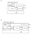
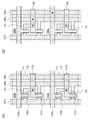
図1(A)に、本発明の一態様に係るPLDの構成例を、模式的に示す。図1(A)に示すPLD100は、複数のPLE(プログラマブルロジックエレメント)101を有するロジックアレイ102と、複数の記憶素子103を有するメモリエレメント104とを有する。メモリエレメント104は、ロジックアレイ102が形成されている層の上に設けられている。
(Embodiment 1)
FIG. 1A schematically illustrates a configuration example of a PLD according to one embodiment of the present invention. A
各PLE101は、実行される論理演算、すなわち入力値に対する出力値の組み合わせが、コンフィギュレーションデータ105に従って定められる論理素子である。コンフィギュレーションデータ105により、各PLE101で行われる論理演算が定められることで、ロジックアレイ102において構成される論理回路の機能が定められる。
Each
メモリエレメント104は、コンフィギュレーションデータ105を記憶する機能を有する。そして、メモリエレメント104には、各記憶素子103に電源電位を供給する複数の配線が設けられている。図1(A)では、配線108及び配線109がメモリエレメント104に設けられている場合を例示している。
The memory element 104 has a function of storing the configuration data 105. The memory element 104 is provided with a plurality of wirings for supplying a power supply potential to each
図1(B)に、記憶素子103の具体的な構成例と、記憶素子103とPLE101との接続構造の一例を、模式的に示す。なお、図1(B)では、複数の記憶素子103のいずれかに相当する、記憶素子103aと記憶素子103bとが、PLE101の一つに対応している場合を例示している。
FIG. 1B schematically illustrates a specific configuration example of the
図1(B)の記憶素子103a及び記憶素子103bで例示するように、記憶素子103は、スイッチ106と、配線107乃至配線109とを有する。配線107は、各記憶素子103にコンフィギュレーションデータ105を送る機能を有する。また、配線108及び配線109は、各記憶素子103に電源電位を供給する機能を有する。なお、図1(B)では、ハイレベルの電源電位を記憶素子103に供給するための配線108と、ローレベルの電源電位を記憶素子103に供給するための配線109とが、各記憶素子103に設けられている場合を例示しているが、電源電位を各記憶素子103に供給するための配線が3つ以上、各記憶素子103に設けられていても良い。
As illustrated by the
また、PLE101と記憶素子103との電気的な接続は、ノード110によって為されている。そして、記憶素子103では、ノード110と配線108及び配線109との間に容量が形成されている。図1(B)では、ノード110と配線108の間に形成される容量を、容量素子111として示し、ノード110と配線109の間に形成される容量を、容量素子112として示す。
In addition, electrical connection between the
なお、本明細書において接続とは電気的な接続を意味しており、電流、電圧または電位が、供給可能、或いは伝送可能な状態に相当する。従って、接続している状態とは、直接接続している状態を必ずしも指すわけではなく、電流、電圧または電位が、供給可能、或いは伝送可能であるように、配線、抵抗、ダイオード、トランジスタなどの素子を介して間接的に接続している状態も、その範疇に含む。 Note that in this specification, connection means electrical connection and corresponds to a state where current, voltage, or a potential can be supplied or transmitted. Therefore, the connected state does not necessarily indicate a directly connected state, and a wiring, a resistor, a diode, a transistor, or the like is provided so that current, voltage, or potential can be supplied or transmitted. The state of being indirectly connected through an element is also included in the category.
配線107によって送られてきたコンフィギュレーションデータ105は、スイッチ106を介してノード110に書き込まれる。具体的には、コンフィギュレーションデータ105によって定められた量の電荷が、オン(導通状態)のスイッチ106を介して配線107からノード110、容量素子111、及び容量素子112に供給されることで、コンフィギュレーションデータ105がノード110に書き込まれる。次いで、スイッチ106がオフ(非導通状態)になり、上記電荷がノード110、容量素子111、及び容量素子112において保持されることで、コンフィギュレーションデータ105が記憶素子103において保持される。そして、スイッチ106を再度オンにすることで、ノード110、容量素子111、及び容量素子112において保持されている電荷を、配線107に放出させることができる。
The configuration data 105 sent via the
PLE101には、ノード110を介して記憶素子103からコンフィギュレーションデータ105が送られる。図1(B)では、記憶素子103a及び記憶素子103bのそれぞれから、一のPLE101にコンフィギュレーションデータ105が送られる構成を例示しているが、3つ以上の記憶素子103から一のPLE101にコンフィギュレーションデータ105が送られる構成としても良い。或いは、一の記憶素子103から一のPLE101にコンフィギュレーションデータ105が送られる構成としても良い。
Configuration data 105 is sent from the
図2(A)に、PLE101の一形態を例示する。図2(A)に示すPLE101は、LUT(ルックアップテーブル)113と、レジスタ114とを有する。LUT113は、コンフィギュレーションデータ105の内容によって、実行される論理演算が異なる。そして、コンフィギュレーションデータ105が確定すると、LUT113は、複数の入力値に対する一の出力値が定まる。そして、LUT113からは、上記出力値を含む出力信号が出力される。レジスタ114は、LUT113からの出力信号を保持し、クロック信号CLKに同期して当該出力信号に対応した信号を出力する。
FIG. 2A illustrates one mode of the
なお、PLE101がさらにマルチプレクサ回路を有し、当該マルチプレクサ回路によって、LUT113からの出力信号がレジスタ114を経由するか否かを選択できるようにしても良い。
Note that the
また、コンフィギュレーションデータ105によって、レジスタ114の種類を定義できる構成にしても良い。具体的には、コンフィギュレーションデータ105によって、レジスタ114がD型レジスタ、T型レジスタ、JK型レジスタ、またはRS型レジスタのいずれかの機能を有するようにしても良い。 Further, the configuration data 105 may be configured so that the type of the register 114 can be defined. Specifically, the configuration data 105 may cause the register 114 to have a function of a D-type register, a T-type register, a JK-type register, or an RS-type register.
また、PLE101が、記憶素子103から送られてきたコンフィギュレーションデータ105を記憶するための記憶装置(コンフィギュレーションメモリ)を有していても良い。図2(B)に示すPLE101は、図2(A)に示したPLE101に、コンフィギュレーションメモリ115をさらに追加した構成を有する。コンフィギュレーションメモリ115を設けることで、同一のコンフィギュレーションデータ105に従って、PLE101にて実行される論理演算を再度定める動作を、記憶素子103から直接送られてきたコンフィギュレーションデータ105を用いる場合よりも、より高速で行うことができる。
The
そして、本発明の一態様では、コンフィギュレーションデータ105が確定した後、別途用意したロジックアレイ102上に、複数のPLE101にコンフィギュレーションデータ105に従って接続されるように、複数の配線を形成することで、半導体装置を作製する。
In one embodiment of the present invention, after the configuration data 105 is determined, a plurality of wirings are formed on the separately
図3(A)に、本発明の一態様に係る半導体装置120の構成例を、模式的に示す。図3(A)に示す半導体装置120は、ロジックアレイ102を有し、当該ロジックアレイ102が複数のPLE101を有する点において、図1(A)に示したPLD100と同じである。しかし、半導体装置120は、メモリエレメント104の代わりに、メモリエレメント104において電源電位の供給に用いられた複数の配線が、当該ロジックアレイ102が形成されている層の上に設けられている点において、図1(A)に示したPLD100と異なっている。
FIG. 3A schematically illustrates a configuration example of the semiconductor device 120 according to one embodiment of the present invention. A semiconductor device 120 illustrated in FIG. 3A includes a
図3(A)では、電源電位の供給に用いられた複数の配線として、配線108及び配線109が、ロジックアレイ102上に設けられている場合を例示している。
FIG. 3A illustrates the case where the
図3(B)に、配線108及び配線109とPLE101との接続構造の一例を、模式的に示す。なお、図3(B)では、図1(B)に示した記憶素子103a及び記憶素子103bが、配線108及び配線109にそれぞれ置き換えられた場合を例示している。
FIG. 3B schematically illustrates an example of a connection structure between the
そして、本発明の一態様に係る半導体装置では、コンフィギュレーションデータ105に従って選択された、配線108及び配線109のいずれか一つと、PLE101とが、ノード110を介して接続されている。具体的に、図3(B)では、記憶素子103aの代わりに設けられた配線108及び配線109のうち、配線108が選択され、当該配線108とPLE101とがノード110を介して接続されている場合を例示している。また、図3(B)では、記憶素子103bの代わりに設けられた配線108及び配線109のうち、配線109が選択され、当該配線109とPLE101とがノード110を介して接続されている場合を例示している。
In the semiconductor device according to one embodiment of the present invention, any one of the
PLE101は、配線108及び配線109から与えられる電源電位に従って、その論理演算が定められる。そして、各PLE101で実行される論理演算が定められることで、ロジックアレイ102において構成される論理回路の機能が定められる。
The logic operation of the
本発明の一態様では、PLD100の上層に設けられたメモリエレメント104を、配線108及び配線109などの複数の配線に置き換えることで、半導体装置120を作製するものである。そして、本発明の一態様では、PLD100のメモリエレメント104に既に上記複数の配線が含まれている。そのため、PLD100と半導体装置120とでは、下層のロジックアレイ102と、上層の複数の配線との間に生じる寄生容量の差が、小さく抑えられる。よって、PLD100の検証によって、上記寄生容量に起因した半導体装置120における消費電力または動作周波数の見積もりを、正確に行うことができる。
In one embodiment of the present invention, the memory element 104 provided in an upper layer of the
なお、コンフィギュレーションデータ105によって定められるのは、PLE101で実行される論理演算だけではない。PLE101どうしの接続構造も、コンフィギュレーションデータ105によって定められる。具体的に、PLE101どうしの接続は、ロジックアレイ102に設けられた配線エレメントによって行われる。配線エレメントは、複数の配線で構成される配線群と、配線群を構成する配線どうしの接続を制御するスイッチとを有する。
Note that the configuration data 105 is not limited to logical operations executed by the
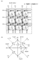
図4(A)にロジックアレイ102の構造の一部を、一例として模式的に示す。図4(A)に示すロジックアレイ102は、複数のPLE101と、複数のPLE101のいずれかに接続された配線群121と、配線群121を構成する配線どうしの接続を制御するスイッチ122とを有する。配線群121及びスイッチ122が、配線エレメント123に相当する。スイッチ122によって制御される配線どうしの接続構造は、コンフィギュレーションデータ105によって定められる。
FIG. 4A schematically illustrates a part of the structure of the
図4(B)に、スイッチ122の構成例を示す。図4(B)に示すスイッチ122は、配線群121に含まれる配線125と配線126の接続構造を制御する機能を有する。具体的に、スイッチ122は、トランジスタ127乃至トランジスタ132を有する。トランジスタ127は、配線125におけるPointAと、配線126におけるPointCの電気的な接続を制御する機能を有する。トランジスタ128は、配線125におけるPointBと、配線126におけるPointCの電気的な接続を制御する機能を有する。トランジスタ129は、配線125におけるPointAと、配線126におけるPointDの電気的な接続を制御する機能を有する。トランジスタ130は、配線125におけるPointBと、配線126におけるPointDの電気的な接続を制御する機能を有する。トランジスタ131は、配線125におけるPointAとPointBの電気的な接続を制御する機能を有する。トランジスタ132は、配線126におけるPointCとPointDの電気的な接続を制御する機能を有する。
FIG. 4B illustrates a configuration example of the
そして、トランジスタ127乃至トランジスタ132のオンまたはオフの選択(スイッチング)は、メモリエレメント104に保持されているコンフィギュレーションデータ105により定まる。具体的に、PLD100の場合、トランジスタ127乃至トランジスタ132のゲート電極は、ノード110を介して複数の記憶素子103にそれぞれ接続されている。また、半導体装置120の場合、トランジスタ127乃至トランジスタ132のゲート電極は、ノード110を介して配線108または配線109に接続されている。
Whether the
また、スイッチ122は、配線群121と、ロジックアレイ102の出力端子124の、電気的な接続を制御する機能を有する。出力端子124は、ロジックアレイ102、メモリエレメント104以外の、PLD100を構成する回路群に、接続される。
In addition, the
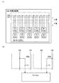
図5に、PLD100における、メモリエレメント104の下層の構成を一例として示す。図5では、メモリエレメント104の下層において、ロジックアレイ102の他に、I/Oエレメント140、PLL(phase lock loop)141、RAM142、乗算器143が設けられている。I/Oエレメント140は、PLD100の外部回路からの信号の入力、または外部回路への信号の出力を制御する、インターフェースとしての機能を有する。PLL141は、クロック信号CLKを生成する機能を有する。RAM142は、論理演算に用いられるデータを格納する機能を有する。乗算器143は、乗算専用の論理回路に相当する。ロジックアレイ102に乗算を行う機能が含まれていれば、乗算器143は必ずしも設ける必要はない。
FIG. 5 shows an example of the configuration of the lower layer of the memory element 104 in the
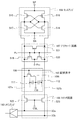
次いで、記憶素子103の具体的な構成例を、図6(A)に模式的に示す。なお、図6(A)では、複数の記憶素子103のいずれかに相当する、記憶素子103aと記憶素子103bとを例示している。
Next, a specific structural example of the
図6(A)の記憶素子103a及び記憶素子103bで例示するように、記憶素子103は、スイッチ106として機能するトランジスタ106tと、配線107乃至配線109と、配線150とを有する。具体的に、トランジスタ106tのゲート電極は、配線150に接続されている。トランジスタ106tのソース端子とドレイン端子は、一方が配線107に接続されており、他方がノード110に接続されている。
As illustrated by the
なお、トランジスタのソース端子とは、活性層の一部であるソース領域、或いは活性層に接続されたソース電極を意味する。同様に、トランジスタのドレイン端子とは、活性層の一部であるドレイン領域、或いは活性層に接続されたドレイン電極を意味する。 Note that a source terminal of a transistor means a source region that is part of an active layer or a source electrode connected to the active layer. Similarly, the drain terminal of a transistor means a drain region that is part of an active layer or a drain electrode connected to the active layer.
トランジスタが有するソース端子とドレイン端子は、トランジスタのチャネル型及び各端子に与えられる電位の高低によって、その呼び方が入れ替わる。一般的に、nチャネル型トランジスタでは、低い電位が与えられる端子がソース端子と呼ばれ、高い電位が与えられる端子がドレイン端子と呼ばれる。また、pチャネル型トランジスタでは、低い電位が与えられる端子がドレイン端子と呼ばれ、高い電位が与えられる端子がソース端子と呼ばれる。本明細書では、便宜上、ソース端子とドレイン端子とが固定されているものと仮定して、トランジスタの接続関係を説明する場合があるが、実際には上記電位の関係に従ってソース端子とドレイン端子の呼び方が入れ替わる。 The names of the source terminal and the drain terminal of the transistor interchange with each other depending on the channel type of the transistor and the level of potential applied to each terminal. In general, in an n-channel transistor, a terminal to which a low potential is applied is called a source terminal, and a terminal to which a high potential is applied is called a drain terminal. In a p-channel transistor, a terminal to which a low potential is applied is called a drain terminal, and a terminal to which a high potential is applied is called a source terminal. In this specification, for the sake of convenience, the connection relationship between transistors may be described on the assumption that the source terminal and the drain terminal are fixed. The name is changed.
また、ノード110と配線108及び配線109との間に容量が形成されている。図6(A)では、ノード110と配線108の間に形成される容量を、容量素子111として示し、ノード110と配線109の間に形成される容量を、容量素子112として示す。ノード110を介して記憶素子103からコンフィギュレーションデータ105が出力される。
Further, a capacitor is formed between the
図6(B)に、図6(A)に示した記憶素子103a及び記憶素子103bが、配線108及び配線109にそれぞれ置き換えられた様子を例示する。図6(B)では、記憶素子103aの代わりに設けられた配線108及び配線109のうち、配線108がコンフィギュレーションデータ105により選択され、当該配線108がノード110に接続されている場合を例示している。また、図6(B)では、記憶素子103bの代わりに設けられた配線108及び配線109のうち、配線109がコンフィギュレーションデータ105により選択され、当該配線109がノード110に接続されている場合を例示している。
FIG. 6B illustrates an example in which the
次いで、図6(A)とは異なる、記憶素子103の具体的な構成例を、図7(A)に模式的に示す。なお、図7(A)では、複数の記憶素子103のいずれかに相当する、記憶素子103aと記憶素子103bとを例示している。
Next, a specific structural example of the
図7(A)の記憶素子103a及び記憶素子103bで例示するように、記憶素子103は、スイッチ106として機能するトランジスタ106tと、配線107乃至配線109と、配線150と、トランジスタ151tとを有する。具体的に、トランジスタ106tのゲート電極は、配線150に接続されている。トランジスタ106tのソース端子とドレイン端子は、一方が配線107に接続されており、他方がノード110に接続されている。トランジスタ151tのゲート電極は、ノード110に接続されている。トランジスタ151tのソース端子とドレイン端子は、一方が配線107に接続されており、他方が接地電位などの固定の電位が与えられているノードに接続されている。
As illustrated by the
また、ノード110と配線108及び配線109との間に容量が形成されている。図7(A)では、ノード110と配線108の間に形成される容量を、容量素子111として示し、ノード110と配線109の間に形成される容量を、容量素子112として示す。ノード110を介して、記憶素子103からコンフィギュレーションデータ105が出力される。また、外部回路からの要求に応じて、記憶素子103に保持されているコンフィギュレーションデータ105を、トランジスタ151tを介して読み出すことができる。
Further, a capacitor is formed between the
図7(B)に、図7(A)に示した記憶素子103a及び記憶素子103bが、配線108及び配線109にそれぞれ置き換えられた様子を例示する。図7(B)では、記憶素子103aの代わりに設けられた配線108及び配線109のうち、配線108がコンフィギュレーションデータ105により選択され、当該配線108がノード110に接続されている場合を例示している。また、図7(B)では、記憶素子103bの代わりに設けられた配線108及び配線109のうち、配線109がコンフィギュレーションデータ105により選択され、当該配線109がノード110に接続されている場合を例示している。
FIG. 7B illustrates an example in which the
なお、図6(A)または図7(A)にて例示した記憶素子103は、必要に応じて、トランジスタ、ダイオード、抵抗素子、容量素子、インダクタなどのその他の回路素子を、さらに有していても良い。
Note that the
また、図6(A)及び図7(A)では、トランジスタ106tがゲート電極を活性層の片側にのみ有している場合を示している。トランジスタ106tが、活性層を間に挟んで存在する一対のゲート電極を有している場合、一方のゲート電極にはスイッチングを制御するための信号が与えられ、他方のゲート電極は、電気的に絶縁しているフローティングの状態であっても良いし、電位が他から与えられている状態であっても良い。後者の場合、一対の電極に、同じ高さの電位が与えられていても良いし、他方のゲート電極にのみ接地電位などの固定電位が与えられていても良い。他方のゲート電極に与える電位の高さを制御することで、トランジスタ106tの閾値電圧を制御することができる。
6A and 7A illustrate the case where the
また、図6(A)または図7(A)にて例示した記憶素子103は、一のトランジスタ106tをスイッチ106として用いている場合について示しているが、本発明はこの構成に限定されない。スイッチ106として機能する複数のトランジスタを用いていても良い。複数のトランジスタがスイッチ106として機能する場合、上記複数のトランジスタは並列に接続されていても良いし、直列に接続されていても良いし、直列と並列が組み合わされて接続されていても良い。
6A and 7A illustrates the case where one
本明細書において、トランジスタが直列に接続されている状態とは、例えば、第1のトランジスタのソース端子またはドレイン端子の一方のみが、第2のトランジスタのソース端子またはドレイン端子の一方のみに接続されている状態を意味する。また、トランジスタが並列に接続されている状態とは、第1のトランジスタのソース端子またはドレイン端子の一方が第2のトランジスタのソース端子またはドレイン端子の一方に接続され、第1のトランジスタのソース端子またはドレイン端子の他方が第2のトランジスタのソース端子またはドレイン端子の他方に接続されている状態を意味する。 In this specification, the state in which the transistors are connected in series means, for example, that only one of the source terminal and the drain terminal of the first transistor is connected to only one of the source terminal and the drain terminal of the second transistor. Means the state. The state in which the transistors are connected in parallel means that one of the source terminal and the drain terminal of the first transistor is connected to one of the source terminal and the drain terminal of the second transistor, and the source terminal of the first transistor Alternatively, the other drain terminal is connected to the other of the source terminal and the drain terminal of the second transistor.
本発明の一態様では、トランジスタ106tの活性層に、非晶質、微結晶、多結晶又は単結晶である、シリコン又はゲルマニウムなどの半導体が用いられていても良いし、酸化物半導体などのワイドギャップの半導体が用いられていても良い。シリコンとしては、プラズマCVD法などの気相成長法若しくはスパッタリング法で作製された非晶質シリコン、非晶質シリコンをレーザーアニールなどの処理により結晶化させた多結晶シリコン、単結晶シリコンウェハに水素イオン等を注入して表層部を剥離した単結晶シリコンなどを用いることができる。
In one embodiment of the present invention, a semiconductor such as silicon or germanium that is amorphous, microcrystalline, polycrystalline, or single crystal may be used for the active layer of the
なお、非特許文献1の場合、Fig.11、Fig.14を参照すると、SRAMを構成するTFTのオフ電流が、ソース端子とドレイン端子間の電圧(ドレイン電圧)が3.3Vのときに1pA程度である。よって、非特許文献1の場合、データを保持するのに費やされるSRAMの消費電力WSRAMは、6.6pW程度と見積もることができる。
In the case of
また、一般的なDRAMに用いられている容量素子の容量値は、20fF程度とされている(Y.Yanagawa,T.Sekiguchi,A.Kotabe,K.Ono,and R.Takemura,「In−substrate−bitline Sense Amplifier with Array−noise−gating Scheme for Low−noise 4F2 DRAM Array Operable at 10−fF Cell Capacitance」、2011 Symposium on VLSI Circuits Digest of Technical Papers,pp.230−231.)。上記容量素子に保持されている電荷量を読み出すことができる配線の寄生容量は、大きく見積もっても、20fFの50倍に相当する1pF程度であると考えられる。本発明の一態様に係るメモリエレメントにおいて、配線107に付加された寄生容量の容量値C107が1pFであり、コンフィギュレーションデータを有する信号のハイレベルの電位Vdataが3.3Vであり、1秒間にN回のリフレッシュを行う場合を想定する。この場合、配線107の電位を電位Vdataに設定するのに費やされる消費電力W107は、(1/2)×C107×Vdata 2×Nで表され、約5.4NpWと見積もることができる。よって、消費電力WSRAMよりも消費電力W107を小さくするためには、Nを約1.2よりも小さく、すなわちリフレッシュの間隔(リフレッシュサイクル)tを約0.8秒より長くする必要がある。
The capacitance value of a capacitor element used in a general DRAM is about 20 fF (Y. Yanagawa, T. Sekiguchi, A. Kotabe, K. Ono, and R. Takemura, “In-substrate”). -Bitline Sense Amplifier with Array-noise-gating Scheme for Low-noise 4F 2 DRAM Array Operatable at 10-fF Cell Capacitance Pc. The parasitic capacitance of the wiring from which the charge amount held in the capacitor element can be read is considered to be about 1 pF corresponding to 50 times 20 fF. In the memory element according to one embodiment of the present invention, the capacitance value C 107 of the parasitic capacitance added to the
また、本発明の一態様に係るメモリエレメントにおいて、記憶素子103に配線108を介して与えられるハイレベルの電源電位VDDを3.3Vとし、ノード110の電位がその半分に達したら、リフレッシュを行う場合を想定する。また、容量素子111の容量値C111を、一般的なDRAMと同程度の20fFとする。トランジスタ106tのオフ電流をIoffとし、リフレッシュの間隔(リフレッシュサイクル)をtとすると、t=C111×VDD×(1/2)/Ioff=33fF/Ioffが成り立つ。よって、tを約0.8秒より長くするためには、Ioffを約40fAより小さくする必要がある。
In the memory element according to one embodiment of the present invention, the high-level power supply potential VDD supplied to the
従って、本発明の一態様では、ドレイン電圧が3.3Vのときに、スイッチ106に用いるトランジスタのオフ電流が40fAより小さいことで、ノード110に保持されている電荷がリークしにくくなり、メモリエレメント104に記憶されているコンフィギュレーションデータを再度書き込む動作(リフレッシュ)の間隔を、長くすることができる。リフレッシュの間隔が長い、すなわち単位時間あたりのリフレッシュの回数が少ないと、リフレッシュに要する消費電力を小さく抑えることができるので、PLD100を元に作製される半導体装置120の消費電力を、PLD100の検証段階においてより正確に見積もることができる。
Therefore, in one embodiment of the present invention, when the drain voltage is 3.3 V, the off-state current of the transistor used for the
なお、トランジスタ106tが酸化物半導体などのバンドギャップが広い半導体をチャネル形成領域に含むことで、オフ電流が極めて小さく、なおかつ高耐圧であるトランジスタ106tを実現することができる。そして、上記構成を有するトランジスタ106tを記憶素子103のスイッチ106として用いることで、通常のシリコンやゲルマニウムなどの半導体で形成されたトランジスタを用いた場合に比べて、ノード110、容量素子111、及び容量素子112に蓄積された電荷のリークを防ぐことができる。
Note that when the
なお、特に断りがない限り、本明細書でオフ電流とは、nチャネル型トランジスタにおいては、ドレイン端子をソース端子とゲート電極よりも高い電位とした状態において、ソース端子の電位を基準としたときのゲート電極の電位が0V以下であるときに、ソース端子とドレイン端子の間に流れる電流のことを意味する。或いは、本明細書でオフ電流とは、pチャネル型トランジスタにおいては、ドレイン端子をソース端子とゲート電極よりも低い電位とした状態において、ソース端子の電位を基準としたときのゲート電極の電位が0V以上であるときに、ソース端子とドレイン端子の間に流れる電流のことを意味する。 Note that unless otherwise specified, off-state current in this specification refers to an n-channel transistor in which the drain terminal is higher than the source terminal and the gate electrode, and the potential of the source terminal is used as a reference. This means a current that flows between the source terminal and the drain terminal when the potential of the gate electrode is 0 V or less. Alternatively, in this specification, off-state current refers to that in a p-channel transistor, the potential of the gate electrode with respect to the potential of the source terminal in a state where the drain terminal is lower than the source terminal and the gate electrode. It means a current flowing between the source terminal and the drain terminal when the voltage is 0 V or higher.
酸化物半導体としては、少なくともインジウム(In)あるいは亜鉛(Zn)を含むことが好ましい。また、該酸化物半導体を用いたトランジスタの電気的特性のばらつきを減らすためのスタビライザーとして、それらに加えてガリウム(Ga)を有することが好ましい。また、スタビライザーとしてスズ(Sn)を有することが好ましい。また、スタビライザーとしてハフニウム(Hf)を有することが好ましい。また、スタビライザーとしてアルミニウム(Al)を有することが好ましい。また、スタビライザーとしてジルコニウム(Zr)を含むことが好ましい。 An oxide semiconductor preferably contains at least indium (In) or zinc (Zn). In addition, it is preferable that gallium (Ga) be included in addition to the stabilizer for reducing variation in electrical characteristics of the transistor including the oxide semiconductor. Moreover, it is preferable to have tin (Sn) as a stabilizer. Moreover, it is preferable to have hafnium (Hf) as a stabilizer. Moreover, it is preferable to have aluminum (Al) as a stabilizer. Moreover, it is preferable that zirconium (Zr) is included as a stabilizer.
また、他のスタビライザーとして、ランタノイドである、ランタン(La)、セリウム(Ce)、プラセオジム(Pr)、ネオジム(Nd)、サマリウム(Sm)、ユウロピウム(Eu)、ガドリニウム(Gd)、テルビウム(Tb)、ジスプロシウム(Dy)、ホルミウム(Ho)、エルビウム(Er)、ツリウム(Tm)、イッテルビウム(Yb)、ルテチウム(Lu)のいずれか一種または複数種を含んでいてもよい。 As other stabilizers, lanthanoids such as lanthanum (La), cerium (Ce), praseodymium (Pr), neodymium (Nd), samarium (Sm), europium (Eu), gadolinium (Gd), terbium (Tb) , Dysprosium (Dy), holmium (Ho), erbium (Er), thulium (Tm), ytterbium (Yb), or lutetium (Lu) may be included.
例えば、酸化物半導体として、酸化インジウム、酸化スズ、酸化亜鉛、二元系金属の酸化物であるIn−Zn系酸化物、Sn−Zn系酸化物、Al−Zn系酸化物、Zn−Mg系酸化物、Sn−Mg系酸化物、In−Mg系酸化物、In−Ga系酸化物、三元系金属の酸化物であるIn−Ga−Zn系酸化物(IGZOとも表記する)、In−Al−Zn系酸化物、In−Sn−Zn系酸化物、Sn−Ga−Zn系酸化物、Al−Ga−Zn系酸化物、Sn−Al−Zn系酸化物、In−Hf−Zn系酸化物、In−La−Zn系酸化物、In−Pr−Zn系酸化物、In−Nd−Zn系酸化物、In−Sm−Zn系酸化物、In−Eu−Zn系酸化物、In−Gd−Zn系酸化物、In−Tb−Zn系酸化物、In−Dy−Zn系酸化物、In−Ho−Zn系酸化物、In−Er−Zn系酸化物、In−Tm−Zn系酸化物、In−Yb−Zn系酸化物、In−Lu−Zn系酸化物、四元系金属の酸化物であるIn−Sn−Ga−Zn系酸化物、In−Hf−Ga−Zn系酸化物、In−Al−Ga−Zn系酸化物、In−Sn−Al−Zn系酸化物、In−Sn−Hf−Zn系酸化物、In−Hf−Al−Zn系酸化物を用いることができる。 For example, as an oxide semiconductor, indium oxide, tin oxide, zinc oxide, binary metal oxides such as In—Zn oxide, Sn—Zn oxide, Al—Zn oxide, Zn—Mg oxide Oxides, Sn—Mg oxides, In—Mg oxides, In—Ga oxides, In—Ga—Zn oxides (also referred to as IGZO) which are oxides of ternary metals, In— Al-Zn oxide, In-Sn-Zn oxide, Sn-Ga-Zn oxide, Al-Ga-Zn oxide, Sn-Al-Zn oxide, In-Hf-Zn oxide In-La-Zn-based oxide, In-Pr-Zn-based oxide, In-Nd-Zn-based oxide, In-Sm-Zn-based oxide, In-Eu-Zn-based oxide, In-Gd -Zn oxide, In-Tb-Zn oxide, In-Dy-Zn oxide, n-Ho-Zn-based oxide, In-Er-Zn-based oxide, In-Tm-Zn-based oxide, In-Yb-Zn-based oxide, In-Lu-Zn-based oxide, quaternary metal In—Sn—Ga—Zn-based oxide, In—Hf—Ga—Zn-based oxide, In—Al—Ga—Zn-based oxide, In—Sn—Al—Zn-based oxide, In— Sn-Hf-Zn-based oxides and In-Hf-Al-Zn-based oxides can be used.
なお、例えば、In−Ga−Zn系酸化物とは、InとGaとZnを含む酸化物という意味であり、InとGaとZnの比率は問わない。また、InとGaとZn以外の金属元素を含んでいてもよい。In−Ga−Zn系酸化物は、無電界時の抵抗が十分に高くオフ電流を十分に小さくすることが可能であり、また、移動度も高い。 Note that for example, an In—Ga—Zn-based oxide means an oxide containing In, Ga, and Zn, and there is no limitation on the ratio of In, Ga, and Zn. Moreover, metal elements other than In, Ga, and Zn may be included. An In—Ga—Zn-based oxide has sufficiently high resistance when no electric field is applied, and can sufficiently reduce off-state current. In addition, the In—Ga—Zn-based oxide has high mobility.
例えば、In:Ga:Zn=1:1:1(=1/3:1/3:1/3)あるいはIn:Ga:Zn=2:2:1(=2/5:2/5:1/5)の原子比のIn−Ga−Zn系酸化物やその組成の近傍の酸化物を用いることができる。あるいは、In:Sn:Zn=1:1:1(=1/3:1/3:1/3)、In:Sn:Zn=2:1:3(=1/3:1/6:1/2)あるいはIn:Sn:Zn=2:1:5(=1/4:1/8:5/8)の原子比のIn−Sn−Zn系酸化物やその組成の近傍の酸化物を用いるとよい。 For example, In: Ga: Zn = 1: 1: 1 (= 1/3: 1/3: 1/3) or In: Ga: Zn = 2: 2: 1 (= 2/5: 2/5: 1). / 5) atomic ratio In—Ga—Zn-based oxides and oxides in the vicinity of the composition can be used. Alternatively, In: Sn: Zn = 1: 1: 1 (= 1/3: 1/3: 1/3), In: Sn: Zn = 2: 1: 3 (= 1/3: 1/6: 1) / 2) or In: Sn: Zn = 2: 1: 5 (= 1/4: 1/8: 5/8) atomic ratio In—Sn—Zn-based oxide or an oxide in the vicinity of the composition. Use it.
例えば、In−Sn−Zn系酸化物では比較的容易に高い移動度が得られる。しかしながら、In−Ga−Zn系酸化物でも、バルク内欠陥密度を低減することにより移動度を上げることができる。 For example, high mobility can be obtained relatively easily with an In—Sn—Zn-based oxide. However, mobility can be increased by reducing the defect density in the bulk also in the case of using an In—Ga—Zn-based oxide.
なお、電子供与体(ドナー)となる水分または水素などの不純物が低減され、なおかつ酸素欠損が低減されることにより高純度化された酸化物半導体(purified Oxide Semiconductor)は、i型(真性半導体)又はi型に限りなく近い。そのため、上記酸化物半導体を用いたトランジスタは、オフ電流が著しく小さいという特性を有する。また、酸化物半導体のバンドギャップは、2eV以上、好ましくは2.5eV以上、より好ましくは3eV以上である。水分または水素などの不純物濃度が十分に低減され、なおかつ酸素欠損が低減されることにより高純度化された酸化物半導体膜を用いることにより、トランジスタのオフ電流を小さくすることができる。 Note that an oxide semiconductor that is highly purified by reducing impurities such as moisture or hydrogen serving as an electron donor (donor) and oxygen vacancies is an i-type (intrinsic semiconductor). Or it is close to i type. Therefore, a transistor including the above oxide semiconductor has a characteristic that off-state current is extremely small. The band gap of the oxide semiconductor is 2 eV or more, preferably 2.5 eV or more, more preferably 3 eV or more. By using the oxide semiconductor film which is highly purified by sufficiently reducing the concentration of impurities such as moisture or hydrogen and reducing oxygen vacancies, the off-state current of the transistor can be reduced.
具体的に、高純度化された酸化物半導体を半導体膜に用いたトランジスタのオフ電流が小さいことは、いろいろな実験により証明できる。例えば、チャネル幅が1×106μmでチャネル長が10μmのトランジスタであっても、ソース端子とドレイン端子間の電圧(ドレイン電圧)が1Vから10Vの範囲において、オフ電流が、半導体パラメータアナライザの測定限界以下、すなわち1×10⁻¹³A以下という特性を得ることができる。この場合、トランジスタのチャネル幅で規格化したオフ電流は、100zA/μm以下である。よって、上記トランジスタの場合、チャネル幅を4×105μmより小さくすることで、酸化物半導体を半導体膜に用いたトランジスタのオフ電流を40fAより小さくすることができる。また、容量素子とトランジスタとを接続して、容量素子に流入または容量素子から流出する電荷を当該トランジスタで制御する回路を用いて、オフ電流の測定を行った。当該測定では、高純度化された酸化物半導体膜を上記トランジスタのチャネル形成領域に用い、容量素子の単位時間あたりの電荷量の推移から当該トランジスタのオフ電流を測定した。その結果、トランジスタのソース端子とドレイン端子間の電圧が3Vの場合に、数十yA/μmという、さらに低いオフ電流が得られることが分かった。従って、高純度化された酸化物半導体膜をチャネル形成領域に用いたトランジスタは、オフ電流が、結晶性を有するシリコンを用いたトランジスタに比べて著しく低い。 Specifically, it can be proved by various experiments that the off-state current of a transistor using a highly purified oxide semiconductor as a semiconductor film is small. For example, even in a transistor having a channel width of 1 × 10 6 μm and a channel length of 10 μm, the off-current is reduced when the voltage between the source terminal and the drain terminal (drain voltage) is in the range of 1V to 10V. It is possible to obtain characteristics that are below the measurement limit, that is, 1 × 10 −13 A or less. In this case, the off-current normalized by the channel width of the transistor is 100 zA / μm or less. Therefore, in the case of the above transistor, the off-state current of a transistor in which an oxide semiconductor is used for a semiconductor film can be reduced to less than 40 fA by reducing the channel width to less than 4 × 10 5 μm. In addition, off-state current was measured using a circuit in which a capacitor and a transistor were connected and charge flowing into or out of the capacitor was controlled by the transistor. In this measurement, a highly purified oxide semiconductor film was used for a channel formation region of the transistor, and the off-state current of the transistor was measured from the change in charge amount per unit time of the capacitor. As a result, it was found that when the voltage between the source terminal and the drain terminal of the transistor is 3 V, an even lower off current of several tens of yA / μm can be obtained. Therefore, a transistor using a highly purified oxide semiconductor film for a channel formation region has significantly lower off-state current than a transistor using crystalline silicon.
本発明の一態様では、オフ電流の極めて小さいトランジスタ106tを用いることで、ノード110、容量素子111、及び容量素子112からの電荷リークを防ぐことができる。よって、本発明の一態様では、ポリシリコンTFTで構成されたSRAMを用いる場合よりも、メモリエレメント104において、トランジスタのオフ電流に起因する消費電力を小さく抑えることができる。そのため、PLD100を元に作製される半導体装置120の消費電力を、PLD100の検証段階において正確に見積もることができる。
In one embodiment of the present invention, charge leakage from the
酸化物半導体膜は、例えば非単結晶を有してもよい。非単結晶は、例えば、CAAC(C Axis Aligned Crystal)、多結晶、微結晶、非晶質部を有する。非晶質部は、微結晶、CAACよりも欠陥準位密度が高い。また、微結晶は、CAACよりも欠陥準位密度が高い。なお、CAACを有する酸化物半導体を、CAAC−OS(C Axis Aligned Crystalline Oxide Semiconductor)と呼ぶ。 For example, the oxide semiconductor film may include a non-single crystal. The non-single crystal includes, for example, CAAC (C Axis Aligned Crystal), polycrystal, microcrystal, and amorphous part. The amorphous part has a higher density of defect states than microcrystals and CAAC. In addition, microcrystals have a higher density of defect states than CAAC. Note that an oxide semiconductor including CAAC is referred to as a CAAC-OS (C Axis Crystallized Oxide Semiconductor).
酸化物半導体膜は、例えばCAAC−OSを有してもよい。CAAC−OSは、例えば、c軸配向し、a軸または/およびb軸はマクロに揃っていない。 For example, the oxide semiconductor film may include a CAAC-OS. For example, the CAAC-OS is c-axis oriented, and the a-axis and / or the b-axis are not aligned macroscopically.
酸化物半導体膜は、例えば微結晶を有してもよい。なお、微結晶を有する酸化物半導体を、微結晶酸化物半導体と呼ぶ。微結晶酸化物半導体膜は、例えば、1nm以上10nm未満のサイズの微結晶(ナノ結晶ともいう。)を膜中に含む。または、微結晶酸化物半導体膜は、例えば、1nm以上10nm未満の結晶部を有する結晶−非晶質混相構造の酸化物半導体を有している。 The oxide semiconductor film may include microcrystal, for example. Note that an oxide semiconductor including microcrystal is referred to as a microcrystalline oxide semiconductor. The microcrystalline oxide semiconductor film includes microcrystal (also referred to as nanocrystal) with a size greater than or equal to 1 nm and less than 10 nm, for example. Alternatively, the microcrystalline oxide semiconductor film includes an oxide semiconductor having a crystal-amorphous mixed phase structure with a crystal part of 1 nm to less than 10 nm, for example.
酸化物半導体膜は、例えば非晶質部を有してもよい。なお、非晶質部を有する酸化物半導体を、非晶質酸化物半導体と呼ぶ。非晶質酸化物半導体膜は、例えば、原子配列が無秩序であり、結晶成分を有さない。または、非晶質酸化物半導体膜は、例えば、完全な非晶質であり、結晶部を有さない。 For example, the oxide semiconductor film may include an amorphous part. Note that an oxide semiconductor having an amorphous part is referred to as an amorphous oxide semiconductor. An amorphous oxide semiconductor film has, for example, disordered atomic arrangement and no crystal component. Alternatively, the amorphous oxide semiconductor film is, for example, completely amorphous and has no crystal part.
なお、酸化物半導体膜が、CAAC−OS、微結晶酸化物半導体、非晶質酸化物半導体の混合膜であってもよい。混合膜は、例えば、非晶質酸化物半導体の領域と、微結晶酸化物半導体の領域と、CAAC−OSの領域と、を有する。また、混合膜は、例えば、非晶質酸化物半導体の領域と、微結晶酸化物半導体の領域と、CAAC−OSの領域と、の積層構造を有してもよい。 Note that the oxide semiconductor film may be a mixed film of a CAAC-OS, a microcrystalline oxide semiconductor, and an amorphous oxide semiconductor. For example, the mixed film includes an amorphous oxide semiconductor region, a microcrystalline oxide semiconductor region, and a CAAC-OS region. The mixed film may have a stacked structure of an amorphous oxide semiconductor region, a microcrystalline oxide semiconductor region, and a CAAC-OS region, for example.
なお、酸化物半導体膜は、例えば、単結晶を有してもよい。 Note that the oxide semiconductor film may include a single crystal, for example.
酸化物半導体膜は、複数の結晶部を有し、当該結晶部のc軸が被形成面の法線ベクトルまたは表面の法線ベクトルに平行な方向に揃っていることが好ましい。なお、異なる結晶部間で、それぞれa軸およびb軸の向きが異なっていてもよい。そのような酸化物半導体膜の一例としては、CAAC−OS膜がある。 The oxide semiconductor film preferably includes a plurality of crystal parts, and the c-axis of the crystal parts is aligned in a direction parallel to the normal vector of the formation surface or the normal vector of the surface. Note that the directions of the a-axis and the b-axis may be different between different crystal parts. An example of such an oxide semiconductor film is a CAAC-OS film.
CAAC−OS膜は、完全な非晶質ではない。CAAC−OS膜は、例えば、結晶部および非晶質部を有する結晶−非晶質混相構造の酸化物半導体を有している。なお、当該結晶部は、一辺が100nm未満の立方体内に収まる大きさであることが多い。また、透過型電子顕微鏡(TEM:Transmission Electron Microscope)による観察像では、CAAC−OS膜に含まれる非晶質部と結晶部との境界、結晶部と結晶部との境界は明確ではない。また、TEMによってCAAC−OS膜には明確な粒界(グレインバウンダリーともいう。)は確認できない。そのため、CAAC−OS膜は、粒界に起因する電子移動度の低下が抑制される。 The CAAC-OS film is not completely amorphous. The CAAC-OS film includes, for example, an oxide semiconductor with a crystal-amorphous mixed phase structure including a crystal part and an amorphous part. Note that the crystal part is often large enough to fit in a cube whose one side is less than 100 nm. Further, in the observation image obtained by a transmission electron microscope (TEM), the boundary between the amorphous part and the crystal part included in the CAAC-OS film and the boundary between the crystal part and the crystal part are not clear. In addition, a clear grain boundary (also referred to as a grain boundary) cannot be confirmed in the CAAC-OS film by TEM. Therefore, in the CAAC-OS film, reduction in electron mobility due to grain boundaries is suppressed.
CAAC−OS膜に含まれる結晶部は、例えば、c軸がCAAC−OS膜の被形成面の法線ベクトルまたは表面の法線ベクトルに平行な方向になるように揃い、かつab面に垂直な方向から見て金属原子が三角形状または六角形状に配列し、c軸に垂直な方向から見て金属原子が層状または金属原子と酸素原子とが層状に配列している。なお、異なる結晶部間で、それぞれa軸およびb軸の向きが異なっていてもよい。本明細書において、単に垂直と記載する場合、80°以上100°以下、好ましくは85°以上95°以下の範囲も含まれることとする。また、単に平行と記載する場合、−10°以上10°以下、好ましくは−5°以上5°以下の範囲も含まれることとする。 The crystal part included in the CAAC-OS film is aligned so that, for example, the c-axis is in a direction parallel to the normal vector of the formation surface of the CAAC-OS film or the normal vector of the surface, and is perpendicular to the ab plane. When viewed from the direction, the metal atoms are arranged in a triangular shape or a hexagonal shape, and when viewed from the direction perpendicular to the c-axis, the metal atoms are arranged in layers, or the metal atoms and oxygen atoms are arranged in layers. Note that the directions of the a-axis and the b-axis may be different between different crystal parts. In this specification, the term “perpendicular” includes a range of 80 ° to 100 °, preferably 85 ° to 95 °. In addition, a simple term “parallel” includes a range of −10 ° to 10 °, preferably −5 ° to 5 °.
なお、CAAC−OS膜において、結晶部の分布が一様でなくてもよい。例えば、CAAC−OS膜の形成過程において、酸化物半導体膜の表面側から結晶成長させる場合、被形成面の近傍に対し表面の近傍では結晶部の占める割合が高くなることがある。また、CAAC−OS膜へ不純物を添加することにより、当該不純物添加領域において結晶部が非晶質化することもある。 Note that the distribution of crystal parts in the CAAC-OS film is not necessarily uniform. For example, in the formation process of the CAAC-OS film, when crystal growth is performed from the surface side of the oxide semiconductor film, the ratio of crystal parts in the vicinity of the surface of the oxide semiconductor film is higher in the vicinity of the surface. In addition, when an impurity is added to the CAAC-OS film, the crystal part in a region to which the impurity is added becomes amorphous in some cases.
CAAC−OS膜に含まれる結晶部のc軸は、CAAC−OS膜の被形成面の法線ベクトルまたは表面の法線ベクトルに平行な方向になるように揃うため、CAAC−OS膜の形状(被形成面の断面形状または表面の断面形状)によっては互いに異なる方向を向くことがある。また、結晶部は、成膜したとき、または成膜後に加熱処理などの結晶化処理を行ったときに形成される。従って、結晶部のc軸は、CAAC−OS膜が形成されたときの被形成面の法線ベクトルまたは表面の法線ベクトルに平行な方向になるように揃う。 Since the c-axis of the crystal part included in the CAAC-OS film is aligned in a direction parallel to the normal vector of the formation surface of the CAAC-OS film or the normal vector of the surface, the shape of the CAAC-OS film ( Depending on the cross-sectional shape of the surface to be formed or the cross-sectional shape of the surface, the directions may be different from each other. The crystal part is formed when a film is formed or when a crystallization process such as a heat treatment is performed after the film formation. Therefore, the c-axes of the crystal parts are aligned in a direction parallel to the normal vector of the surface where the CAAC-OS film is formed or the normal vector of the surface.
CAAC−OS膜を用いたトランジスタは、可視光や紫外光の照射による電気的特性の変動が小さい。よって、当該トランジスタは、信頼性が高い。 In a transistor using a CAAC-OS film, change in electrical characteristics due to irradiation with visible light or ultraviolet light is small. Therefore, the transistor has high reliability.
CAAC−OS膜は、例えば、多結晶である金属酸化物ターゲットを用い、スパッタリング法によって成膜する。当該ターゲットにイオンが衝突すると、ターゲットに含まれる結晶領域がa−b面から劈開し、a−b面に平行な面を有する平板状またはペレット状のスパッタリング粒子として剥離することがある。この場合、当該平板状のスパッタリング粒子が、結晶状態を維持したまま基板に到達することで、CAAC−OS膜を成膜することができる。 The CAAC-OS film is formed by a sputtering method using a polycrystalline metal oxide target, for example. When ions collide with the target, a crystal region included in the target may be cleaved from the ab plane and separated as flat or pellet-like sputtered particles having a plane parallel to the ab plane. In this case, the flat-plate-like sputtered particle reaches the substrate while maintaining a crystalline state, whereby a CAAC-OS film can be formed.
また、CAAC−OS膜を成膜するために、以下の条件を適用することが好ましい。 In order to form the CAAC-OS film, the following conditions are preferably applied.
成膜時の不純物混入を低減することで、不純物によって結晶状態が崩れることを抑制できる。例えば、処理室内に存在する不純物濃度(水素、水、二酸化炭素および窒素など)を低減すればよい。また、成膜ガス中の不純物濃度を低減すればよい。具体的には、露点が−80℃以下、好ましくは−100℃以下である成膜ガスを用いる。 By reducing the mixing of impurities during film formation, the crystal state can be prevented from being broken by impurities. For example, the impurity concentration (hydrogen, water, carbon dioxide, nitrogen, etc.) existing in the treatment chamber may be reduced. Further, the impurity concentration in the deposition gas may be reduced. Specifically, a deposition gas having a dew point of −80 ° C. or lower, preferably −100 ° C. or lower is used.
また、成膜時の基板加熱温度を高めることで、基板到達後にスパッタリング粒子のマイグレーションが起こる。具体的には、基板加熱温度を100℃以上740℃以下、好ましくは200℃以上500℃以下として成膜する。成膜時の基板加熱温度を高めることで、平板状のスパッタリング粒子が基板に到達した場合、基板上でマイグレーションが起こり、スパッタリング粒子の平らな面が基板に付着する。 Further, by increasing the substrate heating temperature during film formation, migration of sputtered particles occurs after reaching the substrate. Specifically, the film is formed at a substrate heating temperature of 100 ° C. to 740 ° C., preferably 200 ° C. to 500 ° C. By increasing the substrate heating temperature at the time of film formation, when the flat sputtered particles reach the substrate, migration occurs on the substrate, and the flat surface of the sputtered particles adheres to the substrate.
また、成膜ガス中の酸素割合を高め、電力を最適化することで成膜時のプラズマダメージを軽減すると好ましい。成膜ガス中の酸素割合は、30体積%以上、好ましくは100体積%とする。 In addition, it is preferable to reduce plasma damage during film formation by increasing the oxygen ratio in the film formation gas and optimizing electric power. The oxygen ratio in the deposition gas is 30% by volume or more, preferably 100% by volume.
ターゲットの一例として、In−Ga−Zn系酸化物ターゲットについて以下に示す。 As an example of the target, an In—Ga—Zn-based oxide target is described below.
InOX粉末、GaOY粉末およびZnOZ粉末を所定のmol数比で混合し、加圧処理後、1000℃以上1500℃以下の温度で加熱処理をすることで多結晶であるIn−Ga−Zn系酸化物ターゲットとする。なお、X、YおよびZは任意の正数である。ここで、所定のmol数比は、例えば、InOX粉末、GaOY粉末およびZnOZ粉末が、2:2:1、8:4:3、3:1:1、1:1:1、4:2:3または3:1:2である。なお、粉末の種類、およびその混合するmol数比は、作製するターゲットによって適宜変更すればよい。 In-Ga-Zn which is polycrystalline by mixing InO X powder, GaO Y powder and ZnO Z powder at a predetermined mol number ratio, and after heat treatment at a temperature of 1000 ° C. to 1500 ° C. A system oxide target is used. X, Y and Z are arbitrary positive numbers. Here, the predetermined mole number ratio is, for example, 2: 2: 1, 8: 4: 3, 3: 1: 1, 1: 1: 1, 4 for InO X powder, GaO Y powder, and ZnO Z powder. : 2: 3 or 3: 1: 2. In addition, what is necessary is just to change suitably the kind of powder, and the mol number ratio to mix with the target to produce.
(実施の形態2)
本実施の形態では、メモリエレメント104の構成例について説明する。
(Embodiment 2)
In this embodiment, a configuration example of the memory element 104 will be described.
図8に、メモリエレメント104の構成を、ブロック図で一例として示す。なお、図8に示すブロック図では、メモリエレメント104内の回路を機能ごとに分類し、互いに独立したブロックとして示しているが、実際の回路は機能ごとに完全に切り分けることが難しく、一つの回路が複数の機能に係わることもあり得る。 FIG. 8 shows a configuration of the memory element 104 as an example in a block diagram. In the block diagram shown in FIG. 8, the circuits in the memory element 104 are classified by function and shown as blocks independent from each other. However, it is difficult to separate an actual circuit for each function. May involve multiple functions.
図8に示すメモリエレメント104は、記憶素子103を複数有するセルアレイ160と、駆動回路161とを有する。そして、駆動回路161は、入出力バッファ162と、メインアンプ163と、カラムデコーダ164と、ローデコーダ165と、スイッチ回路166と、プリチャージ回路167と、センスアンプ168と、書き込み回路169とを有する。
A memory element 104 illustrated in FIG. 8 includes a cell array 160 including a plurality of
入出力バッファ162は、駆動回路161またはセルアレイ160の駆動に用いる各種信号、及び、セルアレイ160に書き込まれるコンフィギュレーションデータの、メモリエレメント104への入力を制御する機能を有する。また、入出力バッファ162は、セルアレイ160から読み出されたコンフィギュレーションデータの、メモリエレメント104からの出力を制御する機能を有する。 The input / output buffer 162 has a function of controlling input of various signals used for driving the driver circuit 161 or the cell array 160 and configuration data written to the cell array 160 to the memory element 104. The input / output buffer 162 has a function of controlling the output from the memory element 104 of configuration data read from the cell array 160.
ローデコーダ165は、例えば図6(A)に示した記憶素子103の場合だと、配線150に与える電位を制御することで、セルアレイ160において記憶素子103を、指定されたアドレスに従って行ごとに選択する機能を有する。カラムデコーダ164は、スイッチ回路166の動作を制御することで、コンフィギュレーションデータの書き込み時、または読み出し時の、列方向における記憶素子103の選択を、指定されたアドレスに従って行う機能を有する。
For example, in the case of the
スイッチ回路166は、例えば図6(A)に示した記憶素子103の場合だと、配線107とメインアンプ163の間の接続と、配線107と書き込み回路169の間の接続とを行う機能を有する。書き込み回路169は、指定されたアドレスの記憶素子103に、スイッチ回路166を介してコンフィギュレーションデータを書き込む機能を有する。
For example, in the case of the
センスアンプ168は、記憶素子103からコンフィギュレーションデータを読み出すときに、配線107の電位の変化を増幅させる機能を有する。また、センスアンプ168は、記憶素子103に書き込まれたコンフィギュレーションデータ、或いは記憶素子103から読み出されたコンフィギュレーションデータを、一時的に記憶する機能を有する。
The sense amplifier 168 has a function of amplifying a change in potential of the
メインアンプ163は、センスアンプ168により増幅された配線107の電位を用いて、コンフィギュレーションデータを読み出す機能を有する。プリチャージ回路167は、コンフィギュレーションデータの読み出し前に、配線107の電位をリセットする機能を有する。
The main amplifier 163 has a function of reading configuration data using the potential of the
なお、メモリエレメント104は、指定された記憶素子103のアドレスを、一時的に記憶することができるアドレスバッファを、有していても良い。
The memory element 104 may include an address buffer that can temporarily store the address of the designated
なお、本発明の一態様では、メモリエレメント104が駆動回路161を必ずしも含んでいる必要はなく、駆動回路161をPLDの外部に設けるようにしても良い。或いは、駆動回路161をロジックアレイ102と同じ層に設け、駆動回路161及びロジックアレイ102上にセルアレイ160を設けるようにしても良い。
Note that in one embodiment of the present invention, the memory element 104 does not necessarily include the driver circuit 161, and the driver circuit 161 may be provided outside the PLD. Alternatively, the driver circuit 161 may be provided in the same layer as the
次いで、図9に、一列の記憶素子103に対応した、センスアンプ168、プリチャージ回路167、スイッチ回路166、及びメインアンプ163の接続構造を例示する。なお、図9では、図6(A)に示した記憶素子103の一つを、例示している。
Next, FIG. 9 illustrates a connection structure of the sense amplifier 168, the precharge circuit 167, the switch circuit 166, and the main amplifier 163 corresponding to the
記憶素子103はトランジスタ106tと容量素子111及び容量素子112とを有している。そして、記憶素子103は、配線107aに接続されている。また、センスアンプ168、プリチャージ回路167、及びスイッチ回路166は、配線107a及び配線107bに接続されている。配線107a及び配線107bは、複数の記憶素子103にそれぞれ接続された複数の配線107の一つに、それぞれ相当するものとする。ただし、配線107a及び配線107bに接続された全ての記憶素子103は、互いに異なる配線150に接続されているものとする。
The
具体的に、図9では、センスアンプ168がラッチ型である場合を例示している。センスアンプ168は、pチャネル型のトランジスタ515及びトランジスタ516と、nチャネル型のトランジスタ517及びトランジスタ518とを有している。トランジスタ515は、ソース端子またはドレイン端子の一方が端子SPに接続され、他方がトランジスタ516及びトランジスタ518のゲート電極と、配線107aとに接続されている。トランジスタ517は、ソース端子またはドレイン端子の一方がトランジスタ516及びトランジスタ518のゲート電極と、配線107aとに接続され、他方が端子SNに接続されている。トランジスタ516は、ソース端子またはドレイン端子の一方が端子SPに接続され、他方がトランジスタ515及びトランジスタ517のゲート電極と、配線107bとに接続されている。トランジスタ518は、ソース端子またはドレイン端子の一方がトランジスタ515及びトランジスタ517のゲート電極と、配線107bとに接続され、他方が端子SNに接続されている。
Specifically, FIG. 9 illustrates the case where the sense amplifier 168 is a latch type. The sense amplifier 168 includes p-
また、プリチャージ回路167は、nチャネル型のトランジスタ519乃至トランジスタ521を有している。トランジスタ519乃至トランジスタ521は、pチャネル型であっても良い。トランジスタ519のソース端子またはドレイン端子は、一方が配線107aに接続され、他方が端子Preに接続されている。トランジスタ520のソース端子またはドレイン端子は、一方が配線107bに接続され、他方が端子Preに接続されている。トランジスタ521のソース端子またはドレイン端子は、一方が配線107aに接続され、他方が配線107bに接続されている。そして、トランジスタ519乃至トランジスタ521は、それぞれのゲート電極が配線PLに接続されている。
The precharge circuit 167 includes n-
スイッチ回路166は、nチャネル型のトランジスタ522及びトランジスタ523を有している。トランジスタ522及びトランジスタ523は、pチャネル型トランジスタであっても良い。トランジスタ522のソース端子またはドレイン端子は、一方が配線107aに接続され、他方が配線IOaに接続されている。トランジスタ523のソース端子またはドレイン端子は、一方が配線107bに接続され、他方が配線IObに接続されている。そして、トランジスタ522及びトランジスタ523は、それぞれのゲート電極が端子CSLに接続されている。端子CSLの電位は、カラムデコーダ164によって制御される。
The switch circuit 166 includes an n-
配線IOa及び配線IObは、メインアンプ163に接続されている。また、書き込み回路169は、コンフィギュレーションデータに従って、配線IOa及び配線IObへの電位の供給を行う機能を有する。 The wiring IOa and the wiring IOb are connected to the main amplifier 163. Further, the writing circuit 169 has a function of supplying a potential to the wiring IOa and the wiring IOb in accordance with the configuration data.
なお、センスアンプ168は上述したようなラッチ型に限定されず、カレントミラー型やシングルエンド型であっても良い。シングルエンド型のセンスアンプ168を用いる場合、配線107bの電位をリセットする必要がないので、プリチャージ回路167においてトランジスタ520及びトランジスタ521を省略することができる。
The sense amplifier 168 is not limited to the latch type as described above, and may be a current mirror type or a single end type. In the case where the single-ended sense amplifier 168 is used, the
また、配線107a及び配線107bの組み合わせは、アレイ方式によって適宜決めることができる。本発明の一態様では、折り返し方式、クロスポイント方式、開放方式などのアレイ方式を用いることができ、これらのアレイ方式に合わせて、複数の記憶素子103にそれぞれ接続された複数の配線107のうち、いずれか2つの配線107と、メインアンプ163とを、スイッチ回路166により接続すれば良い。ただし、上述したように、配線107a及び配線107bに接続された全ての記憶素子103は、互いに異なる配線150に接続されているものとする。
The combination of the
次いで、コンフィギュレーションデータの読み出し時における、図9に示した記憶素子103、センスアンプ168、プリチャージ回路167、スイッチ回路166、及びメインアンプ163の動作の一例について、図10に示したタイミングチャートを用いて説明する。
Next, an example of the operation of the
まず、期間T1では、プリチャージ回路167が有するトランジスタ519乃至トランジスタ521をオンにして、配線107a及び配線107bの電位をリセットする。具体的に、本実施の形態では、配線PLにハイレベルの電位VH_PLを与え、プリチャージ回路167においてトランジスタ519乃至トランジスタ521をオンにする。上記構成により、配線107a及び配線107bに、端子Preの電位Vpreが与えられる。
First, in the period T1, the
なお、期間T1では、端子CSLにはローレベルの電位VL_CSLが与えられており、スイッチ回路166においてトランジスタ522及びトランジスタ523はオフの状態にある。また、配線150(図10のWLに対応)にはローレベルの電位VL_WLが与えられており、記憶素子103においてトランジスタ106tはオフの状態にある。また、端子SP及び端子SNには、電位Vpreが与えられており、センスアンプ168はオフの状態にある。
Note that in the period T1, the low-level potential VL_CSL is applied to the terminal CSL, and the
次いで、配線PLにローレベルの電位VL_PLを与え、プリチャージ回路167においてトランジスタ519乃至トランジスタ521をオフにする。そして、期間T2では、配線150を選択する。具体的に、本実施の形態では、配線150にハイレベルの電位VH_WLを与えることで、配線150を選択し、記憶素子103においてトランジスタ106tをオンにする。上記構成により、配線107aと容量素子111及び容量素子112とがトランジスタ106tを介して接続される。そして、配線107aと容量素子111及び容量素子112とが電気的に接続されると、容量素子111及び容量素子112に保持されている電荷量に従って、配線107aの電位が変動する。
Next, a low-level potential VL_PL is applied to the wiring PL, and the
図10に示すタイミングチャートでは、容量素子111及び容量素子112に蓄積されている電荷量が多い場合を例示している。具体的に、容量素子111及び容量素子112に蓄積されている電荷量が多い場合、容量素子111及び容量素子112から配線107aへ電荷が放出されることで、電位VpreからΔV1だけ配線107aの電位が上昇する。逆に、容量素子111及び容量素子112に蓄積されている電荷量が少ない場合は、配線107aから容量素子111及び容量素子112へ電荷が流入することで、配線107aの電位は電位VpreからΔV2だけ下降する。
The timing chart illustrated in FIG. 10 illustrates the case where the amount of charge accumulated in the
なお、期間T2では、端子CSLにはローレベルの電位VL_CSLが与えられたままであり、スイッチ回路166においてトランジスタ522及びトランジスタ523はオフの状態を維持する。また、端子SP及び端子SNには、電位Vpreが与えられたままであり、センスアンプ168はオフの状態を維持する。
Note that in the period T <b> 2, the low-level potential VL_CSL remains applied to the terminal CSL, and the
次いで、期間T3では、端子SPにハイレベルの電位VH_SPを与え、端子SNにローレベルの電位VL_SNを与えることで、センスアンプ168をオンにする。センスアンプ168は、配線107a及び配線107bの電位差(図10の場合はΔV1)を増幅させる機能を有する。よって、図10に示すタイミングチャートの場合、センスアンプ168がオンになることで、配線107aの電位は、電位Vpre+ΔV1から、端子SPの電位VH_SPに近づいていく。また、配線107bの電位は、電位Vpreから、端子SNの電位VL_SNに近づいていく。
Next, in the period T3, the sense amplifier 168 is turned on by applying the high-level potential VH_SP to the terminal SP and the low-level potential VL_SN to the terminal SN. The sense amplifier 168 has a function of amplifying a potential difference (ΔV1 in the case of FIG. 10) between the
なお、期間T3の開始当初、配線107aの電位が電位Vpre−ΔV2である場合は、センスアンプ168がオンになることで、配線107aの電位は、電位Vpre−ΔV2から、端子SNの電位VL_SNに近づいていく。また、配線107bの電位は、電位Vpreから、端子SPの電位VH_SPに近づいていく。
Note that when the potential of the
なお、期間T3では、配線PLにはローレベルの電位VL_PLが与えられたままであり、プリチャージ回路167においてトランジスタ519乃至トランジスタ521はオフの状態を維持する。また、端子CSLにはローレベルの電位VL_CSLが与えられたままであり、スイッチ回路166においてトランジスタ522及びトランジスタ523はオフの状態を維持する。配線150にはハイレベルの電位VH_WLが与えられたままであり、記憶素子103においてトランジスタ106tはオンの状態を維持する。
Note that in the period T3, the low-level potential VL_PL is kept applied to the wiring PL, and the
次いで、期間T4では、端子CSLに与える電位を制御することで、スイッチ回路166をオンにする。具体的に、本実施の形態では、端子CSLにハイレベルの電位VH_CSLを与え、スイッチ回路166においてトランジスタ522及びトランジスタ523をオンにする。上記構成により、配線107aの電位と、配線107bの電位とが、配線IOa及び配線IObを介してメインアンプ163に与えられる。メインアンプ163では、配線IObの電位に対して配線IOaの電位が高いか低いかにより、出力される電位Voutのレベルが異なる。よって、電位Voutを有する信号には、コンフィギュレーションデータが含まれることになる。
Next, in the period T4, the switch circuit 166 is turned on by controlling the potential applied to the terminal CSL. Specifically, in this embodiment, a high-level potential VH_CSL is supplied to the terminal CSL, and the
なお、期間T4では、配線PLにはローレベルの電位VL_PLが与えられたままであり、プリチャージ回路167においてトランジスタ519乃至トランジスタ521はオフの状態を維持する。また、配線150にはハイレベルの電位VH_WLが与えられたままであり、記憶素子103においてトランジスタ106tはオンの状態を維持する。端子SPにはハイレベルの電位VH_SPが与えられたままであり、端子SNにはローレベルの電位VL_SNが与えられたままであり、センスアンプ168はオンの状態を維持する。
Note that in the period T <b> 4, the low-level potential VL_PL is kept applied to the wiring PL, and the
期間T4が終了すると、端子CSLに与える電位を制御することで、スイッチ回路166をオフにする。具体的に、本実施の形態では、端子CSLにローレベルの電位VL_CSLを与え、スイッチ回路166においてトランジスタ522及びトランジスタ523をオフにする。また、配線150の選択を終了する。具体的に本実施の形態では、配線150にローレベルの電位VL_WLを与えることで、配線150を非選択の状態にし、記憶素子103においてトランジスタ106tをオフにする。
When the period T4 ends, the switch circuit 166 is turned off by controlling the potential applied to the terminal CSL. Specifically, in this embodiment, a low-level potential VL_CSL is applied to the terminal CSL, and the
上述した期間T1乃至期間T4における動作により、記憶素子103からのコンフィギュレーションデータの読み出しが行われる。
The configuration data is read from the
なお、読み出されたコンフィギュレーションデータを再度記憶素子103に書き込む場合、コンフィギュレーションデータの読み出しが行われた後、当該コンフィギュレーションデータの書き込みが再度行われるまで、センスアンプ168をオンの状態に維持しておく。上記構成により、配線107a及び配線107bの電位は、コンフィギュレーションデータの読み出しが行われた後も、センスアンプ168により保持される。そして、コンフィギュレーションデータの読み出しが行われた後、スイッチ回路166においてトランジスタ522及びトランジスタ523をオフにする。次いで、配線150を選択し、トランジスタ106tをオンにすることで、配線107aと容量素子111及び容量素子112を接続する。そして、配線107aの電位に従い容量素子111及び容量素子112に電荷が蓄積されることで、記憶素子103に、読み出されたコンフィギュレーションデータが再度書き込まれる。
Note that when the read configuration data is written to the
また、書き込み回路169から新たなコンフィギュレーションデータを記憶素子103に書き込む場合、まず、端子SPにハイレベルの電位VH_SPを与え、端子SNにローレベルの電位VL_SNを与えることで、センスアンプ168をオンの状態とする。そして、書き込み回路169によって、配線IOa及び配線IObの電位を、コンフィギュレーションデータに従った高さに制御し、スイッチ回路166においてトランジスタ522及びトランジスタ523をオンにする。上記構成により、配線107aに配線IOaの電位が与えられ、配線107bに配線IObの電位が与えられる。次いで、配線150を選択し、トランジスタ106tをオンにすることで、配線107aと容量素子111及び容量素子112を接続する。そして、配線107aの電位に従い容量素子111及び容量素子112に電荷が蓄積されることで、記憶素子103にコンフィギュレーションデータが書き込まれる。
Further, when writing new configuration data from the writing circuit 169 to the
なお、配線107aに配線IOaの電位が与えられ、配線107bに配線IObの電位が与えられた後は、スイッチ回路166においてトランジスタ522及びトランジスタ523をオフにしても、センスアンプ168がオンの状態にあるならば、配線107aの電位と配線107bの電位の高低の関係は、センスアンプ168により保持される。よって、スイッチ回路166においてトランジスタ522及びトランジスタ523をオンからオフに変更するタイミングは、配線150を選択する前であっても、後であっても、どちらでも良い。
Note that after the potential of the wiring IOa is applied to the
本実施の形態は、他の実施の形態と適宜組み合わせて実施することが可能である。 This embodiment can be implemented in appropriate combination with any of the other embodiments.
(実施の形態3)
本実施の形態では、PLE101が有するLUT113の構成例について説明する。LUT113は複数のマルチプレクサを用いて構成することができる。そして、複数のマルチプレクサの入力端子及び制御端子のうちのいずれかにコンフィギュレーションデータ105が入力される構成とすることができる。
(Embodiment 3)
In the present embodiment, a configuration example of the
図11(A)に、PLE101が有するLUT113の一態様を示す。
FIG. 11A illustrates one mode of the
図11(A)において、LUT113は、2入力のマルチプレクサを7つ(マルチプレクサ31、マルチプレクサ32、マルチプレクサ33、マルチプレクサ34、マルチプレクサ35、マルチプレクサ36、マルチプレクサ37)用いて構成されている。マルチプレクサ31乃至マルチプレクサ34の各入力端子が、LUT113の入力端子M1乃至M8に相当する。
In FIG. 11A, the
マルチプレクサ31乃至マルチプレクサ34の各制御端子は電気的に接続されており、上記制御端子が、LUT113の入力端子IN3に相当する。マルチプレクサ31の出力端子、及びマルチプレクサ32の出力端子は、マルチプレクサ35の2つの入力端子と電気的に接続され、マルチプレクサ33の出力端子、及びマルチプレクサ34の出力端子は、マルチプレクサ36の2つの入力端子と電気的に接続されている。マルチプレクサ35及びマルチプレクサ36の各制御端子は電気的に接続されており、上記制御端子が、LUT113の入力端子IN2に相当する。マルチプレクサ35の出力端子、及びマルチプレクサ36の出力端子は、マルチプレクサ37の2つの入力端子と電気的に接続されている。マルチプレクサ37の制御端子は、LUT113の入力端子IN1に相当する。マルチプレクサ37の出力端子がLUT113の出力端子OUTに相当する。
The control terminals of the
入力端子M1乃至入力端子M8に、記憶素子103からコンフィギュレーションデータ105を入力することによって、LUT113によって行われる論理演算の種類を定めることができる。
By inputting the configuration data 105 from the
例えば、図11(A)のLUT113において、入力端子M1乃至入力端子M8に、デジタル値が”0”、”1”、”0”、”1”、”0”、”1”、”1”、”1”であるコンフィギュレーションデータ105をそれぞれ入力した場合、図11(C)に示す等価回路の機能を実現することができる。
For example, in the
図11(B)に、PLE101が有するLUT113の別の一態様を示す。
FIG. 11B illustrates another mode of the
図11(B)において、LUT113は、2入力のマルチプレクサを3つ(マルチプレクサ41、マルチプレクサ42、マルチプレクサ43)と、2入力のOR回路44とを用いて構成されている。
In FIG. 11B, the
マルチプレクサ41の出力端子、及びマルチプレクサ42の出力端子は、マルチプレクサ43の2つの入力端子と電気的に接続されている。OR回路44の出力端子はマルチプレクサ43の制御端子に電気的に接続されている。マルチプレクサ43の出力端子がLUT113の出力端子OUTに相当する。
The output terminal of the
そして、マルチプレクサ41の制御端子A1、入力端子A2及び入力端子A3、マルチプレクサ42の制御端子A6、入力端子A4及び入力端子A5、OR回路44の入力端子A7及び入力端子A8のいずれかに、記憶素子103からコンフィギュレーションデータ105を入力することによって、LUT113によって行われる論理演算の種類を定めることができる。
The memory element is connected to any one of the control terminal A1, the input terminal A2 and the input terminal A3 of the
例えば、図11(B)のLUT113において、入力端子A2、入力端子A4、入力端子A5、制御端子A6、入力端子A8に、記憶素子103から、デジタル値が”0”、”1”、”0”、”0”、”0”であるコンフィギュレーションデータ105をそれぞれ入力した場合、図11(C)に示す等価回路の機能を実現することができる。なお、上記構成の場合、制御端子A1、入力端子A3、入力端子A7がそれぞれ入力端子IN1、入力端子IN2、入力端子IN3に相当する。
For example, in the
なお、図11(A)及び図11(B)では、2入力のマルチプレクサを用いて構成したLUT113の例を示したが、より多くの入力のマルチプレクサを用いて構成したLUT113であっても良い。
11A and 11B show an example of the
また、LUT113は、マルチプレクサの他に、ダイオード、抵抗素子、論理回路(或いは論理素子)、スイッチのいずれかまたは全てを更に有していても良い。論理回路(或いは論理素子)としては、バッファ、インバータ、NAND回路、NOR回路、スリーステートバッファ、クロックドインバータ等を用いることができる。スイッチとしては、例えばアナログスイッチ、トランジスタ等を用いることができる。
In addition to the multiplexer, the
また、図11(A)や図11(B)に示したLUT113を用いて、図11(C)の様な3入力1出力の論理演算を行う場合について示したがこれに限定されない。LUT113及び入力するコンフィギュレーションデータ105を適宜定めることによって、より多くの入力、多くの出力の論理演算を実現することができる。
Further, although the case where a logical operation of three inputs and one output as shown in FIG. 11C is performed using the
本実施の形態は、他の実施の形態と適宜組み合わせて実施することが可能である。 This embodiment can be implemented in appropriate combination with any of the other embodiments.
(実施の形態4)
本実施の形態では、図6(A)に示した記憶素子103において、トランジスタ106tの活性層に酸化物半導体を用い、プログラマブルロジックエレメントが有するトランジスタ230の活性層にシリコンを用いる場合を例に挙げて、PLD及び半導体装置の作製方法について説明する。
(Embodiment 4)
In this embodiment, the case where an oxide semiconductor is used for the active layer of the
ただし、プログラマブルロジックエレメントが有するトランジスタ230は、シリコンの他、ゲルマニウム、シリコンゲルマニウム、単結晶炭化シリコンなどの半導体材料を用いていても良い。また、例えば、シリコンを用いたトランジスタは、シリコンウェハなどの単結晶半導体基板、SOI法により作製されたシリコン薄膜、気相成長法により作製されたシリコン薄膜などを用いて形成することができる。
Note that the
本実施の形態では、まず、図12(A)に示すように、基板700上に絶縁膜701と、単結晶の半導体膜702とを形成する。
In this embodiment, first, as illustrated in FIG. 12A, an insulating
基板700として使用することができる素材に大きな制限はないが、少なくとも、後の加熱処理に耐えうる程度の耐熱性を有していることが必要となる。例えば、基板700には、フュージョン法やフロート法で作製されるガラス基板、石英基板、半導体基板、セラミック基板等を用いることができる。ガラス基板としては、後の加熱処理の温度が高い場合には、歪み点が730℃以上のものを用いると良い。
There is no particular limitation on a material that can be used as the
また、本実施の形態では、半導体膜702が単結晶のシリコンである場合を例に挙げて、以下、プログラマブルロジックエレメントが有するトランジスタの作製方法について説明する。なお、具体的な単結晶の半導体膜702の作製方法の一例について、簡単に説明する。まず、単結晶の半導体基板であるボンド基板に、電界で加速されたイオンでなるイオンビームを注入し、ボンド基板の表面から一定の深さの領域に、結晶構造が乱されることで局所的に脆弱化された脆化層を形成する。脆化層が形成される領域の深さは、イオンビームの加速エネルギーとイオンビームの入射角によって調節することができる。そして、ボンド基板と、絶縁膜701が形成された基板700とを、間に当該絶縁膜701が挟まるように貼り合わせる。貼り合わせは、ボンド基板と基板700とを重ね合わせた後、ボンド基板と基板700の一部に、1N/cm2以上500N/cm2以下、好ましくは11N/cm2以上20N/cm2以下程度の圧力を加える。圧力を加えると、その部分からボンド基板と絶縁膜701とが接合を開始し、最終的には密着した面全体に接合がおよぶ。次いで、加熱処理を行うことで、脆化層に存在する微小ボイドどうしが結合して、微小ボイドの体積が増大する。その結果、脆化層においてボンド基板の一部である単結晶半導体膜が、ボンド基板から分離する。上記加熱処理の温度は、基板700の歪み点を越えない温度とする。そして、上記単結晶半導体膜をエッチング等により所望の形状に加工することで、半導体膜702を形成することができる。
In this embodiment, a method for manufacturing a transistor included in a programmable logic element will be described below by using a case where the
半導体膜702には、閾値電圧を制御するために、硼素、アルミニウム、ガリウムなどのp型の導電性を付与する不純物元素、若しくはリン、砒素などのn型の導電性を付与する不純物元素を添加しても良い。閾値電圧を制御するための不純物元素の添加は、パターニングする前の半導体膜に対して行っても良いし、パターニング後に形成された半導体膜702に対して行っても良い。また、閾値電圧を制御するための不純物元素の添加を、ボンド基板に対して行っても良い。若しくは、不純物元素の添加を、閾値電圧を大まかに調整するためにボンド基板に対して行った上で、閾値電圧を微調整するために、パターニング前の半導体膜に対して、又はパターニングにより形成された半導体膜702に対しても行っても良い。
In order to control the threshold voltage, an impurity element imparting p-type conductivity such as boron, aluminum, or gallium or an impurity element imparting n-type conductivity such as phosphorus or arsenic is added to the
なお、本実施の形態では、単結晶の半導体膜を用いる例について説明しているが、本発明はこの構成に限定されない。例えば、絶縁膜701上に気相成長法を用いて形成された多結晶、微結晶、非晶質の半導体膜を用いても良いし、上記半導体膜を公知の技術により結晶化しても良い。公知の結晶化方法としては、レーザ光を用いたレーザ結晶化法、触媒元素を用いる結晶化法がある。或いは、触媒元素を用いる結晶化法とレーザ結晶化法とを組み合わせて用いることもできる。また、石英のような耐熱性に優れている基板を用いる場合、電熱炉を使用した熱結晶化方法、赤外光を用いたランプアニール結晶化法、触媒元素を用いる結晶化法、950℃程度の高温アニール結晶化法などを用いても良い。
Note that although an example in which a single crystal semiconductor film is used is described in this embodiment, the present invention is not limited to this structure. For example, a polycrystalline, microcrystalline, or amorphous semiconductor film formed over the insulating
次に、図12(B)に示すように、半導体膜702上にゲート絶縁膜703を形成した後、ゲート絶縁膜703上にゲート電極704を形成する。
Next, as illustrated in FIG. 12B, after a
ゲート絶縁膜703は、高密度プラズマ処理、熱処理などを行うことにより半導体膜702の表面を酸化又は窒化することで形成することができる。高密度プラズマ処理は、例えばHe、Ar、Kr、Xeなどの希ガスと酸素、酸化窒素、アンモニア、窒素、水素などの混合ガスとを用いて行う。この場合、プラズマの励起をマイクロ波の導入により行うことで、低電子温度で高密度のプラズマを生成することができる。このような高密度のプラズマで生成された酸素ラジカル(OHラジカルを含む場合もある)や窒素ラジカル(NHラジカルを含む場合もある)によって、半導体膜の表面を酸化又は窒化することにより、1〜20nm、望ましくは5〜10nmの絶縁膜が半導体膜に接するように形成できる。例えば、亜酸化窒素(N2O)をArで1〜3倍(流量比)に希釈して、10Pa〜30Paの圧力にて3kW〜5kWのマイクロ波(2.45GHz)電力を印加して半導体膜702の表面を酸化若しくは窒化させる。この処理により1nm〜10nm(好ましくは2nm〜6nm)の絶縁膜を形成する。更に亜酸化窒素(N2O)とシラン(SiH4)を導入し、10Pa〜30Paの圧力にて3kW〜5kWのマイクロ波(2.45GHz)電力を印加して気相成長法により酸化窒化珪素膜を形成してゲート絶縁膜を形成する。固相反応と気相成長法による反応を組み合わせることにより界面準位密度が低く絶縁耐圧の優れたゲート絶縁膜を形成することができる。
The
上述した高密度プラズマ処理による半導体膜の酸化又は窒化は固相反応で進むため、ゲート絶縁膜703と半導体膜702との界面準位密度を極めて低くすることができる。また高密度プラズマ処理により半導体膜702を直接酸化又は窒化することで、形成される絶縁膜の厚さのばらつきを抑えることができる。また半導体膜が結晶性を有する場合、高密度プラズマ処理を用いて半導体膜の表面を固相反応で酸化させることにより、結晶粒界においてのみ酸化が速く進んでしまうのを抑え、均一性が良く、界面準位密度の低いゲート絶縁膜を形成することができる。高密度プラズマ処理により形成された絶縁膜を、ゲート絶縁膜の一部又は全部に含んで形成されるトランジスタは、特性のばらつきを抑えることができる。
Since the oxidation or nitridation of the semiconductor film by the high-density plasma treatment described above proceeds by a solid phase reaction, the interface state density between the
また、プラズマCVD法又はスパッタリング法などを用い、酸化珪素、窒化酸化珪素、酸化窒化珪素、窒化珪素、酸化ハフニウム、酸化アルミニウム又は酸化タンタル、酸化イットリウム、ハフニウムシリケート(HfSixOy(x>0、y>0))、窒素が添加されたハフニウムシリケート(HfSixOy(x>0、y>0))、窒素が添加されたハフニウムアルミネート(HfAlxOy(x>0、y>0))等を含む膜を、単層で、又は積層させることで、ゲート絶縁膜703を形成しても良い。
Further, using a plasma CVD method, a sputtering method, or the like, silicon oxide, silicon nitride oxide, silicon oxynitride, silicon nitride, hafnium oxide, aluminum oxide or tantalum oxide, yttrium oxide, hafnium silicate (HfSi x O y (x> 0, y> 0)), hafnium silicate with nitrogen added (HfSi x O y (x> 0, y> 0)), hafnium aluminate with nitrogen added (HfAl x O y (x> 0, y> 0) )) And the like may be formed as a single layer or stacked layers to form the
なお、本明細書において酸化窒化物とは、その組成として、窒素よりも酸素の含有量が多い物質であり、また、窒化酸化物とは、その組成として、酸素よりも窒素の含有量が多い物質を意味する。 Note that in this specification, oxynitride is a substance having a higher oxygen content than nitrogen in the composition, and nitride oxide has a nitrogen content higher than oxygen in the composition. Means a substance.
ゲート絶縁膜703の厚さは、例えば、1nm以上100nm以下、好ましくは10nm以上50nm以下とすることができる。本実施の形態では、プラズマCVD法を用いて、膜厚20nm程度の、酸化窒化珪素を含む単層の絶縁膜を形成し、ゲート絶縁膜703として用いる。
The thickness of the
ゲート電極704は、ゲート絶縁膜703を覆うように導電膜を形成した後、該導電膜を所定の形状に加工(パターニング)することで、形成することができる。上記導電膜の形成にはCVD法、スパッタリング法、蒸着法、スピンコート法等を用いることができる。また、導電膜は、タンタル(Ta)、タングステン(W)、チタン(Ti)、モリブデン(Mo)、アルミニウム(Al)、銅(Cu)、クロム(Cr)、ニオブ(Nb)等を用いることができる。上記金属を主成分とする合金を用いても良いし、上記金属を含む化合物を用いても良い。又は、半導体膜に導電性を付与するリン等の不純物元素をドーピングした、多結晶珪素などの半導体を用いて形成しても良い。
The
なお、ゲート電極704は、単層の導電膜で形成されていても良いし、積層された複数の導電膜で形成されていても良い。
Note that the
2つの導電膜の組み合わせとして、1層目に窒化タンタル又はタンタルを、2層目にタングステンを用いることができる。上記例の他に、窒化タングステンとタングステン、窒化モリブデンとモリブデン、アルミニウムとタンタル、アルミニウムとチタン等が挙げられる。タングステンや窒化タンタルは、耐熱性が高いため、2層の導電膜を形成した後の工程において、熱活性化を目的とした加熱処理を行うことができる。また、2層の導電膜の組み合わせとして、例えば、n型の導電性を付与する不純物元素がドーピングされた珪素とニッケルシリサイド、n型の導電性を付与する不純物元素がドーピングされた珪素とタングステンシリサイド等も用いることができる。 As a combination of the two conductive films, tantalum nitride or tantalum can be used for the first layer and tungsten can be used for the second layer. In addition to the above examples, tungsten nitride and tungsten, molybdenum nitride and molybdenum, aluminum and tantalum, aluminum and titanium, and the like can be given. Since tungsten and tantalum nitride have high heat resistance, heat treatment for thermal activation can be performed in the step after forming the two-layer conductive film. Further, as a combination of two conductive films, for example, silicon and nickel silicide doped with an impurity element imparting n-type conductivity, silicon and tungsten silicide doped with an impurity element imparting n-type conductivity Etc. can also be used.
3つの導電膜を積層する3層構造の場合は、モリブデン膜とアルミニウム膜とモリブデン膜の積層構造を採用するとよい。 In the case of a three-layer structure in which three conductive films are stacked, a stacked structure of a molybdenum film, an aluminum film, and a molybdenum film is preferably employed.
また、ゲート電極704に酸化インジウム、酸化インジウム酸化スズ混合物、酸化インジウム酸化亜鉛混合物、酸化亜鉛、酸化亜鉛アルミニウム、酸窒化亜鉛アルミニウム、又は酸化亜鉛ガリウム等の透光性を有する酸化物導電膜を用いることもできる。
The
本実施の形態では、膜厚30nm程度の窒化タンタル上に、膜厚170nm程度のタングステンを積層したゲート電極704を用いる。
In this embodiment, a
なお、マスクを用いずに、液滴吐出法を用いて選択的にゲート電極704を形成しても良い。液滴吐出法とは、所定の組成物を含む液滴を細孔から吐出又は噴出することで所定のパターンを形成する方法を意味し、インクジェット法などがその範疇に含まれる。
Note that the
また、ゲート電極704は、導電膜を形成後、ICP(Inductively Coupled Plasma:誘導結合型プラズマ)エッチング法を用い、エッチング条件(コイル型の電極層に印加される電力量、基板側の電極層に印加される電力量、基板側の電極温度等)を適宜調節することにより、所望のテーパー形状を有するようにエッチングすることができる。また、テーパー形状は、マスクの形状によっても角度等を制御することができる。なお、エッチング用ガスとしては、塩素、塩化硼素、塩化珪素もしくは四塩化炭素などの塩素系ガス、四弗化炭素、弗化硫黄もしくは弗化窒素などのフッ素系ガス又は酸素を適宜用いることができる。
In addition, the
次に、図12(C)に示すように、ゲート電極704をマスクとして一導電性を付与する不純物元素を半導体膜702に添加することで、ゲート電極704と重なるチャネル形成領域705と、チャネル形成領域705を間に挟む一対の不純物領域706とが、半導体膜702に形成される。
Next, as illustrated in FIG. 12C, an impurity element imparting one conductivity is added to the
本実施の形態では、半導体膜702にn型を付与する不純物元素(例えばリン)を添加する場合を例に挙げる。
In this embodiment, the case where an impurity element imparting n-type conductivity (eg, phosphorus) is added to the
次いで、図12(D)に示すように、ゲート絶縁膜703、ゲート電極704を覆うように、絶縁膜707、絶縁膜708、及び絶縁膜709を形成する。具体的に、絶縁膜707、絶縁膜708、及び絶縁膜709は、酸化珪素、窒化珪素、窒化酸化珪素、酸化窒化珪素、窒化アルミニウム、窒化酸化アルミニウムなどの無機の絶縁膜を用いることができる。特に、誘電率の低い(low−k)材料を絶縁膜707、絶縁膜708、及び絶縁膜709に用いることで、各種電極や配線の重なりに起因する容量を十分に低減することが可能になるため好ましい。なお、絶縁膜707、絶縁膜708、及び絶縁膜709に、上記材料を用いた多孔性の絶縁膜を適用しても良い。多孔性の絶縁膜では、密度の高い絶縁膜と比較して誘電率が低下するため、電極や配線に起因する寄生容量を更に低減することが可能である。
Next, as illustrated in FIG. 12D, an insulating
本実施の形態では、絶縁膜707として膜厚50nmの酸化窒化珪素膜、絶縁膜708として膜厚100nm程度の窒化酸化珪素膜、絶縁膜709として膜厚450nmの酸化窒化珪素膜を用いる場合を例に挙げる。また、本実施の形態では、ゲート電極704上に絶縁膜707、絶縁膜708、及び絶縁膜709を形成している場合を例示しているが、本発明はゲート電極704上に絶縁膜を1層だけ形成していても良いし、3層以外の複数の絶縁膜を積層するように形成していても良い。
In this embodiment, a silicon oxynitride film with a thickness of 50 nm is used as the insulating
次いで、図13(A)に示すように、エッチング等によりゲート絶縁膜703、絶縁膜707、絶縁膜708、及び絶縁膜709に開口部を形成し、一対の各不純物領域706の一部、及びゲート電極704の一部を露出させた後、一対の各不純物領域706に接する導電膜710及び導電膜711と、ゲート電極704に接する導電膜712とを形成する。そして、導電膜710乃至導電膜712を覆うように、絶縁膜709上に絶縁膜713を形成する。
Next, as illustrated in FIG. 13A, an opening is formed in the
導電膜710乃至導電膜712となる導電膜は、アルミニウム、クロム、銅、タンタル、チタン、モリブデン、タングステンから選ばれた元素、又は上述した元素を成分とする合金か、上述した元素を組み合わせた合金膜等が挙げられる。また、アルミニウム、銅などの金属膜の下側もしくは上側にクロム、タンタル、チタン、モリブデン、タングステンなどの高融点金属膜を積層させた構成としても良い。また、アルミニウム又は銅は、耐熱性や腐食性の問題を回避するために、高融点金属材料と組み合わせて用いると良い。高融点金属材料としては、モリブデン、チタン、クロム、タンタル、タングステン、ネオジム、スカンジウム、イットリウム等を用いることができる。
The conductive film to be the
また、導電膜710乃至導電膜712となる導電膜は、単層構造でも、2層以上の積層構造としてもよい。例えば、シリコンを含むアルミニウム膜の単層構造、アルミニウム膜上にチタン膜を積層する2層構造、チタン膜と、そのチタン膜上に重ねてアルミニウム膜を積層し、更にその上にチタン膜を成膜する3層構造などが挙げられる。
The conductive films to be the
また、導電膜710乃至導電膜712となる導電膜としては、導電性の金属酸化物で形成しても良い。導電性の金属酸化物としては酸化インジウム、酸化スズ、酸化亜鉛、酸化インジウム酸化スズ混合物、酸化インジウム酸化亜鉛混合物又は前記金属酸化物材料にシリコン若しくは酸化シリコンを含ませたものを用いることができる。
Alternatively, the conductive film to be the
本実施の形態では、膜厚50nm程度のチタン膜と、膜厚200nm程度のアルミニウム膜と、膜厚100nm程度のチタン膜とを積層させた導電膜を、導電膜710乃至導電膜712として用いる。
In this embodiment, a conductive film in which a titanium film with a thickness of about 50 nm, an aluminum film with a thickness of about 200 nm, and a titanium film with a thickness of about 100 nm are stacked is used as the
絶縁膜713は単層構造でも2層以上の積層構造でもよいが、その表面は高い平坦性を有することが好ましい。絶縁膜713として、例えば、酸化珪素、窒化珪素、酸化窒化珪素、窒化酸化珪素などを用いることができる。そして、絶縁膜713は、プラズマCVD法、光CVD法、熱CVD法などのCVD法を用いて形成することができる。
The insulating
また、絶縁膜713として、有機シランを用いて化学気相成長法により作製される酸化珪素膜を用いることもできる。有機シランとしては、珪酸エチル(TEOS:Si(OC2H5)4)、トリメチルシラン(TMS:(CH3)3SiH)、テトラメチルシクロテトラシロキサン(TMCTS)、オクタメチルシクロテトラシロキサン(OMCTS)、ヘキサメチルジシラザン(HMDS)、トリエトキシシラン(SiH(OC2H5)3)、トリスジメチルアミノシラン(SiH(N(CH3)2)3)等を用いることができる。もちろん、モノシラン、ジシラン、又はトリシラン等の無機シランを用いて、酸化珪素、酸化窒化珪素、窒化珪素、窒化酸化珪素などを形成しても良い。
Alternatively, as the insulating
本実施の形態では、TEOSを用いて、膜厚1.5μm程度の酸化珪素を含む絶縁膜713を形成する。
In this embodiment, an insulating
以上の工程により、プログラマブルロジックエレメントが有するトランジスタ230を形成することができる。トランジスタ230は、半導体膜702と、半導体膜702上のゲート絶縁膜703と、ゲート絶縁膜703上において半導体膜702と重なる位置に形成されたゲート電極704と、半導体膜702が有する不純物領域706に接続された、ソース電極またはドレイン電極として機能する導電膜710及び導電膜711とを有する。
Through the above process, the
次いで、図13(B)に示すように、絶縁膜713にCMP(化学的機械研磨)処理やエッチング処理を行うことにより、導電膜712の表面を露出させる。なお、後に形成されるトランジスタ106tの特性を向上させるために、絶縁膜713の表面は可能な限り平坦にしておくことが好ましい。
Next, as illustrated in FIG. 13B, the surface of the
次いで、トランジスタ106tの作製方法について説明する。まず、図13(C)に示すように、絶縁膜713及び導電膜712上に、絶縁膜714を形成した後、絶縁膜714上に酸化物半導体膜715を形成する。
Next, a method for manufacturing the
絶縁膜714は、絶縁膜707乃至絶縁膜709と同様の材料を用いて形成することができる。本実施の形態では、膜厚300nm程度の酸化窒化珪素膜を、絶縁膜714として用いる。
The insulating
酸化物半導体膜715は、絶縁膜714上に形成した酸化物半導体膜を所望の形状に加工することで、形成することができる。上記酸化物半導体膜の膜厚は、2nm以上200nm以下、好ましくは3nm以上50nm以下、更に好ましくは3nm以上20nm以下とする。酸化物半導体膜は、酸化物半導体をターゲットとして用い、スパッタ法により成膜する。また、酸化物半導体膜は、希ガス(例えばアルゴン)雰囲気下、酸素雰囲気下、又は希ガス(例えばアルゴン)及び酸素混合雰囲気下においてスパッタ法により形成することができる。
The
なお、酸化物半導体膜をスパッタ法により成膜する前に、アルゴンガスを導入してプラズマを発生させる逆スパッタを行い、絶縁膜714の表面に付着している塵埃を除去することが好ましい。逆スパッタとは、ターゲット側に電圧を印加せずに、アルゴン雰囲気下で基板側にRF電源を用いて電圧を印加して基板近傍にプラズマを形成して表面を改質する方法である。なお、アルゴン雰囲気に代えて窒素、ヘリウムなどを用いてもよい。また、アルゴン雰囲気に酸素、亜酸化窒素などを加えた雰囲気で行ってもよい。また、アルゴン雰囲気に塩素、四フッ化炭素などを加えた雰囲気で行ってもよい。
Note that before the oxide semiconductor film is formed by a sputtering method, reverse sputtering that generates plasma by introducing argon gas is preferably performed to remove dust attached to the surface of the insulating
例えば、酸化物半導体として、酸化インジウム、酸化スズ、酸化亜鉛、二元系金属の酸化物であるIn−Zn系酸化物、Sn−Zn系酸化物、Al−Zn系酸化物、Zn−Mg系酸化物、Sn−Mg系酸化物、In−Mg系酸化物、In−Ga系酸化物、三元系金属の酸化物であるIn−Ga−Zn系酸化物(IGZOとも表記する)、In−Al−Zn系酸化物、In−Sn−Zn系酸化物、Sn−Ga−Zn系酸化物、Al−Ga−Zn系酸化物、Sn−Al−Zn系酸化物、In−Hf−Zn系酸化物、In−La−Zn系酸化物、In−Pr−Zn系酸化物、In−Nd−Zn系酸化物、In−Sm−Zn系酸化物、In−Eu−Zn系酸化物、In−Gd−Zn系酸化物、In−Tb−Zn系酸化物、In−Dy−Zn系酸化物、In−Ho−Zn系酸化物、In−Er−Zn系酸化物、In−Tm−Zn系酸化物、In−Yb−Zn系酸化物、In−Lu−Zn系酸化物、四元系金属の酸化物であるIn−Sn−Ga−Zn系酸化物、In−Hf−Ga−Zn系酸化物、In−Al−Ga−Zn系酸化物、In−Sn−Al−Zn系酸化物、In−Sn−Hf−Zn系酸化物、In−Hf−Al−Zn系酸化物を用いることができる。 For example, as an oxide semiconductor, indium oxide, tin oxide, zinc oxide, binary metal oxides such as In—Zn oxide, Sn—Zn oxide, Al—Zn oxide, Zn—Mg oxide Oxides, Sn—Mg oxides, In—Mg oxides, In—Ga oxides, In—Ga—Zn oxides (also referred to as IGZO) which are oxides of ternary metals, In— Al-Zn oxide, In-Sn-Zn oxide, Sn-Ga-Zn oxide, Al-Ga-Zn oxide, Sn-Al-Zn oxide, In-Hf-Zn oxide In-La-Zn-based oxide, In-Pr-Zn-based oxide, In-Nd-Zn-based oxide, In-Sm-Zn-based oxide, In-Eu-Zn-based oxide, In-Gd -Zn oxide, In-Tb-Zn oxide, In-Dy-Zn oxide, n-Ho-Zn-based oxide, In-Er-Zn-based oxide, In-Tm-Zn-based oxide, In-Yb-Zn-based oxide, In-Lu-Zn-based oxide, quaternary metal In—Sn—Ga—Zn-based oxide, In—Hf—Ga—Zn-based oxide, In—Al—Ga—Zn-based oxide, In—Sn—Al—Zn-based oxide, In— Sn-Hf-Zn-based oxides and In-Hf-Al-Zn-based oxides can be used.
本実施の形態では、In(インジウム)、Ga(ガリウム)、及びZn(亜鉛)を含むターゲットを用いたスパッタ法により得られる膜厚30nmのIn−Ga−Zn系酸化物半導体の薄膜を、酸化物半導体膜として用いる。上記ターゲットとして、好ましくは、原子数比がIn:Ga:Zn=1:1:1、4:2:3、3:1:2、1:1:2、2:1:3、または3:1:4で示されるターゲットを用いる。また、In、Ga、及びZnを含むターゲットの充填率は90%以上100%以下、好ましくは95%以上100%未満である。充填率の高いターゲットを用いることにより、成膜した酸化物半導体膜は緻密な膜となる。 In this embodiment, a 30 nm-thick In—Ga—Zn-based oxide semiconductor thin film obtained by sputtering using a target containing In (indium), Ga (gallium), and Zn (zinc) is oxidized. Used as a physical semiconductor film. As the above target, the atomic ratio is preferably In: Ga: Zn = 1: 1: 1, 4: 2: 3, 3: 1: 2, 1: 1: 2, 2: 1: 3, or 3: A target shown as 1: 4 is used. The filling rate of the target containing In, Ga, and Zn is 90% to 100%, preferably 95% to less than 100%. By using a target with a high filling rate, the formed oxide semiconductor film becomes a dense film.
なお、酸化物半導体膜としてIn−Zn系の材料を用いる場合、用いるターゲット中の金属元素の原子数比は、In:Zn=50:1〜1:2(モル数比に換算するとIn2O3:ZnO=25:1〜1:4)、好ましくはIn:Zn=20:1〜1:1(モル数比に換算するとIn2O3:ZnO=10:1〜1:2)、さらに好ましくはIn:Zn=15:1〜1.5:1(モル数比に換算するとIn2O3:ZnO=15:2〜3:4)とする。例えば、In−Zn系酸化物半導体の形成に用いるターゲットは、原子数比がIn:Zn:O=X:Y:Zのとき、Z>1.5X+Yとする。Znの比率を上記範囲に収めることで、移動度の向上を実現することができる。 Note that in the case where an In—Zn-based material is used for the oxide semiconductor film, the atomic ratio of metal elements in the target to be used is In: Zn = 50: 1 to 1: 2 (in 2 O converted to a molar ratio). 3 : ZnO = 25: 1 to 1: 4), preferably In: Zn = 20: 1 to 1: 1 (In 2 O 3 : ZnO = 10: 1 to 1: 2 in terms of molar ratio), Preferably, In: Zn = 15: 1 to 1.5: 1 (In 2 O 3 : ZnO = 15: 2 to 3: 4 in terms of molar ratio). For example, a target used for forming an In—Zn-based oxide semiconductor satisfies Z> 1.5X + Y when the atomic ratio is In: Zn: O = X: Y: Z. By keeping the Zn ratio in the above range, the mobility can be improved.
また、酸化物半導体膜としてIn−Sn−Zn系酸化物半導体膜をスパッタリング法で成膜する場合、金属元素の原子数比がIn:Sn:Zn=1:1:1、2:1:3、1:2:2、または4:9:7で示されるIn−Sn−Zn系酸化物ターゲットを用いる。 In the case where an In—Sn—Zn-based oxide semiconductor film is formed as the oxide semiconductor film by a sputtering method, the atomic ratio of metal elements is In: Sn: Zn = 1: 1: 1, 2: 1: 3. 1: 2: 2, or 4: 9: 7, an In—Sn—Zn-based oxide target is used.
本実施の形態では、減圧状態に保持された処理室内に基板を保持し、処理室内の残留水分を除去しつつ水素及び水分が除去されたスパッタガスを導入し、上記ターゲットを用いて酸化物半導体膜を成膜する。成膜時に、基板温度を100℃以上600℃以下、好ましくは200℃以上400℃以下としても良い。基板を加熱しながら成膜することにより、成膜した酸化物半導体膜に含まれる不純物濃度を低減することができる。また、スパッタリングによる損傷が軽減される。処理室内の残留水分を除去するためには、吸着型の真空ポンプを用いることが好ましい。例えば、クライオポンプ、イオンポンプ、チタンサブリメーションポンプを用いることが好ましい。また、排気手段としては、ターボポンプにコールドトラップを加えたものであってもよい。クライオポンプを用いて処理室を排気すると、例えば、水素原子、水(H2O)など水素原子を含む化合物(より好ましくは炭素原子を含む化合物も)等が排気されるため、当該処理室で成膜した酸化物半導体膜に含まれる不純物の濃度を低減できる。 In this embodiment, a substrate is held in a treatment chamber kept under reduced pressure, a sputtering gas from which hydrogen and moisture are removed is introduced while moisture remaining in the treatment chamber is removed, and an oxide semiconductor is formed using the above target. A film is formed. At the time of film formation, the substrate temperature may be 100 ° C. or higher and 600 ° C. or lower, preferably 200 ° C. or higher and 400 ° C. or lower. By forming the film while heating the substrate, the concentration of impurities contained in the formed oxide semiconductor film can be reduced. Further, damage due to sputtering is reduced. In order to remove moisture remaining in the treatment chamber, an adsorption-type vacuum pump is preferably used. For example, it is preferable to use a cryopump, an ion pump, or a titanium sublimation pump. The exhaust means may be a turbo pump provided with a cold trap. When a processing chamber is exhausted using a cryopump, for example, a compound containing a hydrogen atom (more preferably a compound containing a carbon atom) such as a hydrogen atom or water (H 2 O) is exhausted. The concentration of impurities contained in the formed oxide semiconductor film can be reduced.
成膜条件の一例としては、基板とターゲットの間との距離を100mm、圧力0.6Pa、直流(DC)電源0.5kW、酸素(酸素流量比率100%)雰囲気下の条件が適用される。なお、パルス直流(DC)電源を用いると、成膜時に発生する塵埃が軽減でき、膜厚分布も均一となるために好ましい。 As an example of the film forming conditions, the distance between the substrate and the target is 100 mm, the pressure is 0.6 Pa, the direct current (DC) power source is 0.5 kW, and the oxygen (oxygen flow rate is 100%) atmosphere is applied. Note that a pulse direct current (DC) power source is preferable because dust generated in film formation can be reduced and the film thickness can be made uniform.
また、スパッタリング装置の処理室のリークレートを1×10⁻¹⁰Pa・m3/秒以下とすることで、スパッタリング法による成膜途中における酸化物半導体膜への、アルカリ金属、水素化物等の不純物の混入を低減することができる。また、排気系として上述した吸着型の真空ポンプを用いることで、排気系からのアルカリ金属、水素原子、水素分子、水、水酸基、または水素化物等の不純物の逆流を低減することができる。 Further, by setting the leak rate of the processing chamber of the sputtering apparatus to 1 × 10 −10 Pa · m 3 / sec or less, impurities such as alkali metal and hydride to the oxide semiconductor film during the film formation by the sputtering method Can be reduced. Further, by using the above-described adsorption-type vacuum pump as an exhaust system, backflow of impurities such as alkali metal, hydrogen atom, hydrogen molecule, water, hydroxyl group, or hydride from the exhaust system can be reduced.
また、ターゲットの純度を、99.99%以上とすることで、酸化物半導体膜に混入するアルカリ金属、水素原子、水素分子、水、水酸基、または水素化物等を低減することができる。また、当該ターゲットを用いることで、酸化物半導体膜において、リチウム、ナトリウム、カリウム等のアルカリ金属の濃度を低減することができる。 In addition, when the purity of the target is 99.99% or higher, alkali metals, hydrogen atoms, hydrogen molecules, water, hydroxyl groups, hydrides, or the like mixed in the oxide semiconductor film can be reduced. In addition, when the target is used, the concentration of alkali metal such as lithium, sodium, or potassium can be reduced in the oxide semiconductor film.
なお、酸化物半導体膜に水素、水酸基及び水分がなるべく含まれないようにするために、成膜の前処理として、スパッタリング装置の予備加熱室で絶縁膜714までが形成された基板700を予備加熱し、基板700に吸着した水分又は水素などの不純物を脱離し排気することが好ましい。なお、予備加熱の温度は、100℃以上400℃以下、好ましくは150℃以上300℃以下である。また、予備加熱室に設ける排気手段はクライオポンプが好ましい。なお、この予備加熱の処理は省略することもできる。また、この予備加熱は、後に行われるゲート絶縁膜719の成膜前に、導電膜717及び導電膜718まで形成した基板700にも同様に行ってもよい。
Note that in order to prevent the oxide semiconductor film from containing hydrogen, a hydroxyl group, and moisture as much as possible, as a pretreatment for film formation, the
なお、酸化物半導体膜715を形成するためのエッチングは、ドライエッチングでもウェットエッチングでもよく、両方を用いてもよい。ドライエッチングに用いるエッチングガスとしては、塩素を含むガス(塩素系ガス、例えば塩素(Cl2)、三塩化硼素(BCl3)、四塩化珪素(SiCl4)、四塩化炭素(CCl4)など)が好ましい。また、フッ素を含むガス(フッ素系ガス、例えば四弗化炭素(CF4)、六弗化硫黄(SF6)、三弗化窒素(NF3)、トリフルオロメタン(CHF3)など)、臭化水素(HBr)、酸素(O2)、これらのガスにヘリウム(He)やアルゴン(Ar)などの希ガスを添加したガス、などを用いることができる。
Note that the etching for forming the
ドライエッチング法としては、平行平板型RIE(Reactive Ion Etching)法や、ICP(Inductively Coupled Plasma:誘導結合型プラズマ)エッチング法を用いることができる。所望の形状にエッチングできるように、エッチング条件(コイル型の電極に印加される電力量、基板側の電極に印加される電力量、基板側の電極温度等)を適宜調節する。 As the dry etching method, a parallel plate RIE (Reactive Ion Etching) method or an ICP (Inductively Coupled Plasma) etching method can be used. Etching conditions (such as the amount of power applied to the coil-type electrode, the amount of power applied to the substrate-side electrode, and the substrate-side electrode temperature) are adjusted as appropriate so that etching can be performed in a desired shape.
ウェットエッチングに用いるエッチング液として、燐酸と酢酸と硝酸を混ぜた溶液、クエン酸やシュウ酸などの有機酸を用いることができる。本実施の形態では、ITO−07N(関東化学社製)を用いる。 As an etchant used for wet etching, a mixed solution of phosphoric acid, acetic acid, and nitric acid, or an organic acid such as citric acid or oxalic acid can be used. In this embodiment, ITO-07N (manufactured by Kanto Chemical Co., Inc.) is used.
酸化物半導体膜715を形成するためのレジストマスクをインクジェット法で形成してもよい。レジストマスクをインクジェット法で形成するとフォトマスクを使用しないため、製造コストを低減できる。
A resist mask for forming the
なお、次工程の導電膜を形成する前に逆スパッタを行い、酸化物半導体膜715及び絶縁膜714の表面に付着しているレジスト残渣などを除去することが好ましい。
Note that before the conductive film in the next step is formed, reverse sputtering is preferably performed to remove a resist residue or the like attached to the surfaces of the
なお、スパッタ等で成膜された酸化物半導体膜中には、不純物としての水分又は水素(水酸基を含む)が多量に含まれていることがある。水分又は水素はドナー準位を形成しやすいため、酸化物半導体にとっては不純物である。そこで、本発明の一態様では、酸化物半導体膜中の水分又は水素などの不純物を低減(脱水化または脱水素化)するために、酸化物半導体膜715に対して、減圧雰囲気下、窒素や希ガスなどの不活性ガス雰囲気下、酸素ガス雰囲気下、又は超乾燥エア(CRDS(キャビティリングダウンレーザー分光法)方式の露点計を用いて測定した場合の水分量が20ppm(露点換算で−55℃)以下、好ましくは1ppm以下、好ましくは10ppb以下の空気)雰囲気下で、酸化物半導体膜715に加熱処理を施す。
Note that an oxide semiconductor film formed by sputtering or the like may contain a large amount of moisture or hydrogen (including a hydroxyl group) as an impurity. Since moisture or hydrogen easily forms a donor level, it is an impurity for an oxide semiconductor. Therefore, in one embodiment of the present invention, in order to reduce (dehydration or dehydrogenation) impurities such as moisture or hydrogen in the oxide semiconductor film, the
酸化物半導体膜715に加熱処理を施すことで、酸化物半導体膜715中の水分又は水素を脱離させることができる。具体的には、250℃以上750℃以下、好ましくは400℃以上基板の歪み点未満の温度で加熱処理を行えば良い。例えば、500℃、3分間以上6分間以下程度で行えばよい。加熱処理にRTA法を用いれば、短時間に脱水化又は脱水素化が行えるため、ガラス基板の歪点を超える温度でも処理することができる。
By performing heat treatment on the
本実施の形態では、加熱処理装置の一つである電気炉を用いる。 In this embodiment, an electric furnace which is one of heat treatment apparatuses is used.
なお、加熱処理装置は電気炉に限られず、抵抗発熱体などの発熱体からの熱伝導又は熱輻射によって、被処理物を加熱する装置を備えていてもよい。例えば、GRTA(Gas Rapid Thermal Anneal)装置、LRTA(Lamp Rapid Thermal Anneal)装置等のRTA(Rapid Thermal Anneal)装置を用いることができる。LRTA装置は、ハロゲンランプ、メタルハライドランプ、キセノンアークランプ、カーボンアークランプ、高圧ナトリウムランプ、高圧水銀ランプなどのランプから発する光(電磁波)の輻射により、被処理物を加熱する装置である。GRTA装置は、高温のガスを用いて加熱処理を行う装置である。気体には、アルゴンなどの希ガス、又は窒素のような、加熱処理によって被処理物と反応しない不活性気体が用いられる。 Note that the heat treatment apparatus is not limited to an electric furnace, and may include a device for heating an object to be processed by heat conduction or heat radiation from a heating element such as a resistance heating element. For example, a rapid thermal annealing (RTA) device such as a GRTA (Gas Rapid Thermal Anneal) device or an LRTA (Lamp Rapid Thermal Anneal) device can be used. The LRTA apparatus is an apparatus that heats an object to be processed by radiation of light (electromagnetic waves) emitted from a lamp such as a halogen lamp, a metal halide lamp, a xenon arc lamp, a carbon arc lamp, a high pressure sodium lamp, or a high pressure mercury lamp. The GRTA apparatus is an apparatus that performs heat treatment using a high-temperature gas. As the gas, an inert gas that does not react with an object to be processed by heat treatment, such as nitrogen or a rare gas such as argon, is used.
加熱処理においては、窒素、又はヘリウム、ネオン、アルゴン等の希ガスに、水分又は水素などが含まれないことが好ましい。又は、加熱処理装置に導入する窒素、又はヘリウム、ネオン、アルゴン等の希ガスの純度を、6N(99.9999%)以上、好ましくは7N(99.99999%)以上、(即ち不純物濃度を1ppm以下、好ましくは0.1ppm以下)とすることが好ましい。 In the heat treatment, it is preferable that moisture, hydrogen, or the like be not contained in nitrogen or a rare gas such as helium, neon, or argon. Alternatively, the purity of nitrogen or a rare gas such as helium, neon, or argon introduced into the heat treatment apparatus is 6N (99.9999%) or more, preferably 7N (99.99999%) or more (that is, the impurity concentration is 1 ppm). Or less, preferably 0.1 ppm or less).
以上の工程により、酸化物半導体膜715中の水素の濃度を低減し、高純度化することができる。それにより酸化物半導体膜の安定化を図ることができる。また、ガラス転移温度以下の加熱処理で、キャリア密度が極端に少なく、バンドギャップの広い酸化物半導体膜を形成することができる。このため、大面積基板を用いてトランジスタを作製することができ、量産性を高めることができる。また、当該水素濃度が低減され高純度化された酸化物半導体膜を用いることで、耐圧性が高く、オフ電流の著しく低いトランジスタを作製することができる。上記加熱処理は、酸化物半導体膜の成膜以降であれば、いつでも行うことができる。
Through the above steps, the concentration of hydrogen in the
なお、酸化物半導体膜は非晶質であっても良いが、結晶性を有していても良い。結晶性を有する酸化物半導体膜としては、c軸配向を有した結晶(CAAC)を含むCAAC−OS(C Axis Aligned Crystalline Oxide Semiconductor)膜であっても、トランジスタの信頼性を高めるという効果を得ることができるので、好ましい。 Note that the oxide semiconductor film may be amorphous or may have crystallinity. Even if the oxide semiconductor film having crystallinity is a CAAC-OS (C Axis Crystalline Oxide Semiconductor) film including a crystal having a c-axis orientation (CAAC), an effect of improving the reliability of the transistor is obtained. This is preferable.
CAAC−OS膜で構成された酸化物半導体膜は、スパッタリング法によっても作製することができる。スパッタリング法によってCAAC−OS膜を得るには酸化物半導体膜の堆積初期段階において六方晶の結晶が形成されるようにすることと、当該結晶を種として結晶が成長されるようにすることが肝要である。そのためには、ターゲットと基板の距離を広くとり(例えば、150mm〜200mm程度)、基板加熱温度を100℃〜500℃、好適には200℃〜400℃、さらに好適には250℃〜300℃にすると好ましい。また、これに加えて、成膜時の基板加熱温度よりも高い温度で、堆積された酸化物半導体膜を熱処理することで膜中に含まれるミクロな欠陥や、積層界面の欠陥を修復することができる。 An oxide semiconductor film including a CAAC-OS film can be formed by a sputtering method. In order to obtain a CAAC-OS film by a sputtering method, it is important to form hexagonal crystals in the initial stage of deposition of the oxide semiconductor film and to grow crystals using the crystals as seeds. It is. For that purpose, the distance between the target and the substrate is increased (for example, about 150 mm to 200 mm), and the substrate heating temperature is 100 ° C. to 500 ° C., preferably 200 ° C. to 400 ° C., more preferably 250 ° C. to 300 ° C. It is preferable. In addition to this, the deposited oxide semiconductor film is heat-treated at a temperature higher than the substrate heating temperature at the time of film formation to repair micro defects contained in the film and defects at the lamination interface. Can do.
次いで、図14(A)に示すように、絶縁膜713及び絶縁膜714に、エッチング等により開口部を形成することで導電膜710の一部を露出させた後、開口部において導電膜710に接し、なおかつ酸化物半導体膜715に接する導電膜717と、酸化物半導体膜715に接する導電膜718とを形成する。導電膜717及び導電膜718は、ソース電極又はドレイン電極として機能する。
Next, as illustrated in FIG. 14A, an opening is formed in the insulating
具体的に、導電膜717及び導電膜718は、開口部を覆うようにスパッタ法や真空蒸着法で絶縁膜714上に導電膜を形成した後、当該導電膜を所定の形状に加工(パターニング)することで、形成することができる。
Specifically, the
導電膜717及び導電膜718となる導電膜は、アルミニウム、クロム、銅、タンタル、チタン、モリブデン、タングステンから選ばれた元素、又は上述した元素を成分とする合金か、上述した元素を組み合わせた合金膜等が挙げられる。また、アルミニウム、銅などの金属膜の下側もしくは上側にクロム、タンタル、チタン、モリブデン、タングステンなどの高融点金属膜を積層させた構成としても良い。また、アルミニウム又は銅は、耐熱性や腐食性の問題を回避するために、高融点金属材料と組み合わせて用いると良い。高融点金属材料としては、モリブデン、チタン、クロム、タンタル、タングステン、ネオジム、スカンジウム、イットリウム等を用いることができる。
The conductive film to be the
また、導電膜717及び導電膜718となる導電膜は、単層構造でも、2層以上の積層構造としてもよい。例えば、シリコンを含むアルミニウム膜の単層構造、アルミニウム膜上にチタン膜を積層する2層構造、チタン膜と、そのチタン膜上に重ねてアルミニウム膜を積層し、更にその上にチタン膜を成膜する3層構造などが挙げられる。また、Cu−Mg−Al合金、Mo−Ti合金、Ti、Mo、は、酸化膜との密着性が高い。よって、下層にCu−Mg−Al合金、Mo−Ti合金、Ti、或いはMoで構成される導電膜、上層にCuで構成される導電膜を積層し、上記積層された導電膜を導電膜717及び導電膜718に用いることで、酸化膜である絶縁膜714と、導電膜717及び導電膜718との密着性を高めることができる。
The conductive film to be the
また、導電膜717及び導電膜718となる導電膜としては、導電性の金属酸化物で形成しても良い。導電性の金属酸化物としては酸化インジウム、酸化スズ、酸化亜鉛、酸化インジウム酸化スズ混合物、酸化インジウム酸化亜鉛混合物又は前記金属酸化物材料にシリコン若しくは酸化シリコンを含ませたものを用いることができる。
Alternatively, the conductive film to be the
導電膜形成後に加熱処理を行う場合には、この加熱処理に耐える耐熱性を導電膜に持たせることが好ましい。 In the case where heat treatment is performed after formation of the conductive film, the conductive film preferably has heat resistance enough to withstand the heat treatment.
本実施の形態では、導電膜717及び導電膜718として、膜厚150nmのタングステン膜を用いる。
In this embodiment, a 150-nm-thick tungsten film is used as the
なお、導電膜のエッチングの際に、酸化物半導体膜715がなるべく除去されないようにそれぞれの材料及びエッチング条件を適宜調節する。エッチング条件によっては、酸化物半導体膜715の露出した部分が一部エッチングされることで、溝部(凹部)が形成されることもある。
Note that each material and etching conditions are adjusted as appropriate so that the
本実施の形態では、導電膜717及び導電膜718となる導電膜に、タングステン膜を用いる。そのため、アンモニアと過酸化水素水を含む溶液(アンモニア過水)を用いて、選択的に上記導電膜をウェットエッチングすることができる。具体的には、31重量%の過酸化水素水と、28重量%のアンモニア水と、水とを、体積比5:2:2で混合したアンモニア過水を用いる。或いは、四弗化炭素(CF4)、塩素(Cl2)、酸素を含むガスを用いて、上記導電膜をドライエッチングしても良い。
In this embodiment, a tungsten film is used for the conductive films to be the
なお、フォトリソグラフィ工程で用いるフォトマスク数及び工程数を削減するため、透過した光に多段階の強度をもたせる多階調マスクによって形成されたレジストマスクを用いてエッチング工程を行ってもよい。多階調マスクを用いて形成したレジストマスクは複数の膜厚を有する形状となり、エッチングを行うことで更に形状を変形することができるため、異なるパターンに加工する複数のエッチング工程に用いることができる。よって、一枚の多階調マスクによって、少なくとも二種類以上の異なるパターンに対応するレジストマスクを形成することができる。よって露光マスク数を削減することができ、対応するフォトリソグラフィ工程も削減できるため、工程の簡略化が可能となる。 Note that in order to reduce the number of photomasks used in the photolithography process and the number of processes, the etching process may be performed using a resist mask formed by a multi-tone mask that gives multi-level intensity to transmitted light. A resist mask formed using a multi-tone mask has a shape with a plurality of thicknesses, and the shape can be further deformed by etching. Therefore, the resist mask can be used for a plurality of etching processes for processing into different patterns. . Therefore, a resist mask corresponding to at least two kinds of different patterns can be formed by using one multi-tone mask. Therefore, the number of exposure masks can be reduced, and the corresponding photolithography process can be reduced, so that the process can be simplified.
また、酸化物半導体膜715と、ソース電極又はドレイン電極として機能する導電膜717及び導電膜718との間に、ソース領域及びドレイン領域として機能する酸化物導電膜を設けるようにしても良い。酸化物導電膜の材料としては、酸化亜鉛を成分として含むものが好ましく、酸化インジウムを含まないものであることが好ましい。そのような酸化物導電膜として、酸化亜鉛、酸化亜鉛アルミニウム、酸窒化亜鉛アルミニウム、酸化亜鉛ガリウムなどを適用することができる。
An oxide conductive film functioning as a source region and a drain region may be provided between the
例えば、酸化物導電膜を形成する場合、酸化物導電膜を形成するためのパターニングと、導電膜717及び導電膜718を形成するためのパターニングとを一括で行うようにしても良い。
For example, in the case of forming an oxide conductive film, patterning for forming the oxide conductive film and patterning for forming the
ソース領域及びドレイン領域として機能する酸化物導電膜を設けることで、酸化物半導体膜715と導電膜717及び導電膜718の間の抵抗を下げることができるので、トランジスタの高速動作を実現させることができる。また、ソース領域及びドレイン領域として機能する酸化物導電膜を設けることで、トランジスタの耐圧を高めることができる。
By providing the oxide conductive film functioning as the source region and the drain region, the resistance between the
次いで、N2O、N2、又はArなどのガスを用いたプラズマ処理を行うようにしても良い。このプラズマ処理によって露出している酸化物半導体膜の表面に付着した水などを除去する。また、酸素とアルゴンの混合ガスを用いてプラズマ処理を行ってもよい。 Next, plasma treatment using a gas such as N 2 O, N 2 , or Ar may be performed. Water or the like attached to the surface of the oxide semiconductor film exposed by this plasma treatment is removed. Further, plasma treatment may be performed using a mixed gas of oxygen and argon.
なお、プラズマ処理を行った後、図14(B)に示すように、導電膜717及び導電膜718と、酸化物半導体膜715とを覆うように、ゲート絶縁膜719を形成する。そして、ゲート絶縁膜719上において、酸化物半導体膜715と重なる位置にゲート電極720を形成し、導電膜717と重なる位置に導電膜721を形成する。
Note that after the plasma treatment, a
ゲート絶縁膜719は、ゲート絶縁膜703と同様の材料、同様の積層構造を用いて形成することが可能である。なお、ゲート絶縁膜719は、水分や、水素などの不純物を極力含まないことが望ましく、単層の絶縁膜であっても良いし、積層された複数の絶縁膜で構成されていても良い。ゲート絶縁膜719に水素が含まれると、その水素が酸化物半導体膜715へ侵入し、又は水素が酸化物半導体膜715中の酸素を引き抜き、酸化物半導体膜715が低抵抗化(n型化)してしまい、寄生チャネルが形成されるおそれがある。よって、ゲート絶縁膜719はできるだけ水素を含まない膜になるように、成膜方法に水素を用いないことが重要である。上記ゲート絶縁膜719には、バリア性の高い材料を用いるのが望ましい。例えば、バリア性の高い絶縁膜として、窒化珪素膜、窒化酸化珪素膜、窒化アルミニウム膜、又は窒化酸化アルミニウム膜などを用いることができる。複数の積層された絶縁膜を用いる場合、窒素の含有比率が低い酸化珪素膜、酸化窒化珪素膜などの絶縁膜を、上記バリア性の高い絶縁膜よりも、酸化物半導体膜715に近い側に形成する。そして、窒素の含有比率が低い絶縁膜を間に挟んで、導電膜717及び導電膜718及び酸化物半導体膜715と重なるように、バリア性の高い絶縁膜を形成する。バリア性の高い絶縁膜を用いることで、酸化物半導体膜715内、ゲート絶縁膜719内、或いは、酸化物半導体膜715と他の絶縁膜の界面とその近傍に、水分又は水素などの不純物が入り込むのを防ぐことができる。また、酸化物半導体膜715に接するように窒素の比率が低い酸化珪素膜、酸化窒化珪素膜などの絶縁膜を形成することで、バリア性の高い材料を用いた絶縁膜が直接酸化物半導体膜715に接するのを防ぐことができる。
The
本実施の形態では、スパッタ法で形成された膜厚30nmの酸化窒化珪素膜をゲート絶縁膜719として用いる。成膜時の基板温度は、室温以上400℃以下とすればよく、本実施の形態では300℃とする。
In this embodiment, a 30-nm-thick silicon oxynitride film formed by a sputtering method is used as the
なお、ゲート絶縁膜719を形成した後に、加熱処理を施しても良い。加熱処理は、窒素、超乾燥空気、又は希ガス(アルゴン、ヘリウムなど)の雰囲気下において、好ましくは200℃以上400℃以下、例えば250℃以上350℃以下で行う。上記ガスは、水の含有量が20ppm以下、好ましくは1ppm以下、より好ましくは10ppb以下であることが望ましい。本実施の形態では、例えば、窒素雰囲気下で250℃、1時間の加熱処理を行う。或いは、導電膜717及び導電膜718を形成する前に、水分又は水素を低減させるための酸化物半導体膜に対して行った先の加熱処理と同様に、高温短時間のRTA処理を行っても良い。酸素を含むゲート絶縁膜719が設けられた後に、加熱処理が施されることによって、酸化物半導体膜715に対して行った先の加熱処理により、酸化物半導体膜715に酸素欠損が発生していたとしても、ゲート絶縁膜719から酸化物半導体膜715に酸素が供与される。そして、酸化物半導体膜715に酸素が供与されることで、酸化物半導体膜715において、ドナーとなる酸素欠損を低減し、化学量論的組成を満たすことが可能である。酸化物半導体膜には化学量論的組成を超える量の酸素が含まれていることが好ましい。その結果、酸化物半導体膜715をi型に近づけることができ、酸素欠損によるトランジスタの電気的特性のばらつきを軽減し、電気的特性の向上を実現することができる。この加熱処理を行うタイミングは、ゲート絶縁膜719の形成後であれば特に限定されず、他の工程、例えば樹脂膜形成時の加熱処理や、透明導電膜を低抵抗化させるための加熱処理と兼ねることで、工程数を増やすことなく、酸化物半導体膜715をi型に近づけることができる。
Note that heat treatment may be performed after the
また、酸素雰囲気下で酸化物半導体膜715に加熱処理を施すことで、酸化物半導体に酸素を添加し、酸化物半導体膜715中においてドナーとなる酸素欠損を低減させても良い。加熱処理の温度は、例えば100℃以上350℃未満、好ましくは150℃以上250℃未満で行う。上記酸素雰囲気下の加熱処理に用いられる酸素ガスには、水、水素などが含まれないことが好ましい。又は、加熱処理装置に導入する酸素ガスの純度を、6N(99.9999%)以上、好ましくは7N(99.99999%)以上、(即ち酸素中の不純物濃度を1ppm以下、好ましくは0.1ppm以下)とすることが好ましい。
Alternatively, oxygen vacancies serving as donors in the
或いは、イオン注入法又はイオンドーピング法などを用いて、酸化物半導体膜715に酸素を添加することで、ドナーとなる酸素欠損を低減させても良い。例えば、2.45GHzのマイクロ波でプラズマ化した酸素を酸化物半導体膜715に添加すれば良い。
Alternatively, oxygen vacancies serving as donors may be reduced by adding oxygen to the
また、ゲート電極720及び導電膜721は、ゲート絶縁膜719上に導電膜を形成した後、該導電膜をパターニングすることで形成することができる。ゲート電極720及び導電膜721は、ゲート電極704、或いは導電膜717及び導電膜718と同様の材料を用いて形成することが可能である。
The
ゲート電極720及び導電膜721の膜厚は、10nm〜400nm、好ましくは100nm〜300nmとする。本実施の形態では、タングステンターゲットを用いたスパッタ法により150nmのゲート電極用の導電膜を形成した後、該導電膜をエッチングにより所望の形状に加工(パターニング)することで、ゲート電極720及び導電膜721を形成する。なお、レジストマスクをインクジェット法で形成してもよい。レジストマスクをインクジェット法で形成するとフォトマスクを使用しないため、製造コストを低減できる。
The thicknesses of the
以上の工程により、トランジスタ106tが形成される。
Through the above steps, the
なお、ゲート絶縁膜719を間に挟んで導電膜717と導電膜721とが重なる部分が、容量素子111に相当する。なお、本実施の形態では容量素子112を図示していないが、容量素子111と同様に、ゲート絶縁膜719を間に挟んで導電膜717と重なる導電膜を、導電膜721とは別にゲート絶縁膜719上に設けることで、容量素子112を形成することができる。
Note that a portion where the
また、トランジスタ106tはシングルゲート構造のトランジスタを用いて説明したが、必要に応じて、電気的に接続された複数のゲート電極を有することで、チャネル形成領域を複数有する、マルチゲート構造のトランジスタも形成することができる。
Although the
なお、酸化物半導体膜715に接する絶縁膜(本実施の形態においては、絶縁膜714及びゲート絶縁膜719が該当する。)は、第13族元素及び酸素を含む絶縁材料を用いるようにしても良い。酸化物半導体材料には第13族元素を含むものが多く、第13族元素を含む絶縁材料は酸化物半導体との相性が良く、これを酸化物半導体膜に接する絶縁膜に用いることで、酸化物半導体膜との界面の状態を良好に保つことができる。
Note that as the insulating film in contact with the oxide semiconductor film 715 (in this embodiment, the insulating
第13族元素を含む絶縁材料とは、絶縁材料に一又は複数の第13族元素を含むことを意味する。第13族元素を含む絶縁材料としては、例えば、酸化ガリウム、酸化アルミニウム、酸化アルミニウムガリウム、酸化ガリウムアルミニウムなどがある。ここで、酸化アルミニウムガリウムとは、ガリウムの含有量(原子%)よりアルミニウムの含有量(原子%)が多いものを示し、酸化ガリウムアルミニウムとは、ガリウムの含有量(原子%)がアルミニウムの含有量(原子%)以上のものを示す。 An insulating material containing a Group 13 element means that the insulating material contains one or more Group 13 elements. Examples of the insulating material containing a Group 13 element include gallium oxide, aluminum oxide, aluminum gallium oxide, and gallium aluminum oxide. Here, aluminum gallium oxide indicates that the aluminum content (atomic%) is higher than gallium content (atomic%), and gallium aluminum oxide means that the gallium aluminum content (atomic%) contains aluminum. The amount (atomic%) or more is shown.
例えば、ガリウムを含有する酸化物半導体膜に接して絶縁膜を形成する場合に、絶縁膜に酸化ガリウムを含む材料を用いることで酸化物半導体膜と絶縁膜の界面特性を良好に保つことができる。例えば、酸化物半導体膜と酸化ガリウムを含む絶縁膜とを接して設けることにより、酸化物半導体膜と絶縁膜の界面における水素のパイルアップを低減することができる。なお、絶縁膜に酸化物半導体の成分元素と同じ族の元素を用いる場合には、同様の効果を得ることが可能である。例えば、酸化アルミニウムを含む材料を用いて絶縁膜を形成することも有効である。なお、酸化アルミニウムは、水を透過させにくいという特性を有しているため、当該材料を用いることは、酸化物半導体膜への水の侵入防止という点においても好ましい。 For example, when an insulating film is formed in contact with an oxide semiconductor film containing gallium, the interface characteristics between the oxide semiconductor film and the insulating film can be kept favorable by using a material containing gallium oxide for the insulating film. . For example, when the oxide semiconductor film and the insulating film containing gallium oxide are provided in contact with each other, hydrogen pileup at the interface between the oxide semiconductor film and the insulating film can be reduced. Note that a similar effect can be obtained when an element of the same group as a constituent element of the oxide semiconductor is used for the insulating film. For example, it is also effective to form an insulating film using a material containing aluminum oxide. Note that aluminum oxide has a characteristic that water does not easily permeate, and thus the use of the material is preferable in terms of preventing water from entering the oxide semiconductor film.
また、酸化物半導体膜715に接する絶縁膜は、酸素雰囲気下による熱処理や、酸素ドープなどにより、絶縁材料を化学量論的組成より酸素が多い状態とすることが好ましい。酸素ドープとは、酸素をバルクに添加することをいう。なお、当該バルクの用語は、酸素を薄膜表面のみでなく薄膜内部に添加することを明確にする趣旨で用いている。また、酸素ドープには、プラズマ化した酸素をバルクに添加する酸素プラズマドープが含まれる。また、酸素ドープは、イオン注入法又はイオンドーピング法を用いて行ってもよい。
The insulating film in contact with the
酸素ドープ処理を行うことにより、化学量論的組成より酸素が多い領域を有する絶縁膜を形成することができる。このような領域を備える絶縁膜と酸化物半導体膜が接することにより、絶縁膜中の過剰な酸素が酸化物半導体膜に供給され、酸化物半導体膜中、又は酸化物半導体膜と絶縁膜の界面における酸素欠陥を低減し、酸化物半導体膜をi型化又はi型に限りなく近くすることができる。 By performing oxygen doping treatment, an insulating film having a region where oxygen is higher than that in the stoichiometric composition can be formed. When the insulating film including such a region is in contact with the oxide semiconductor film, excess oxygen in the insulating film is supplied to the oxide semiconductor film, and the oxide semiconductor film or the interface between the oxide semiconductor film and the insulating film is supplied. The number of oxygen defects can be reduced, and the oxide semiconductor film can be made i-type or i-type as close as possible.
なお、化学量論的組成より酸素が多い領域を有する絶縁膜は、酸化物半導体膜715に接する絶縁膜のうち、上層に位置する絶縁膜又は下層に位置する絶縁膜のうち、どちらか一方のみに用いても良いが、両方の絶縁膜に用いる方が好ましい。化学量論的組成より酸素が多い領域を有する絶縁膜を、酸化物半導体膜715に接する絶縁膜の、上層及び下層に位置する絶縁膜に用い、酸化物半導体膜715を挟む構成とすることで、上記効果をより高めることができる。
Note that the insulating film having a region containing more oxygen than the stoichiometric composition has only one of the insulating film in contact with the
また、酸化物半導体膜715の上層又は下層に用いる絶縁膜は、上層と下層で同じ構成元素を有する絶縁膜としても良いし、異なる構成元素を有する絶縁膜としても良い。また、酸化物半導体膜715に接する絶縁膜は、化学量論的組成より酸素が多い領域を有する絶縁膜の積層としても良い。
The insulating film used for the upper layer or the lower layer of the
次に、図14(C)に示すように、ゲート絶縁膜719、導電膜721、ゲート電極720を覆うように、絶縁膜722を形成する。絶縁膜722は、PVD法やCVD法などを用いて形成することができる。また、酸化珪素、酸化窒化珪素、窒化珪素、酸化ハフニウム、酸化ガリウム、酸化アルミニウム等の無機絶縁材料を含む材料を用いて形成することができる。なお、絶縁膜722には、誘電率の低い材料や、誘電率の低い構造(多孔性の構造など)を用いることが望ましい。絶縁膜722の誘電率を低くすることにより、配線や電極などの間に生じる寄生容量を低減し、動作の高速化を図ることができるためである。なお、本実施の形態では、絶縁膜722を単層構造としているが、本発明の一態様はこれに限定されず、2層以上の積層構造としても良い。
Next, as illustrated in FIG. 14C, an insulating
次に、ゲート絶縁膜719、絶縁膜722に開口部725を形成し、導電膜721の一部を露出させる。その後、絶縁膜722上に、上記開口部725において導電膜721と接する配線726を形成する。
Next, an
配線726は、PVD法や、CVD法を用いて導電膜を形成した後、当該導電膜をパターニングすることによって形成される。また、導電膜の材料としては、アルミニウム、クロム、銅、タンタル、チタン、モリブデン、タングステンから選ばれた元素や、上述した元素を成分とする合金等を用いることができる。マンガン、マグネシウム、ジルコニウム、ベリリウム、ネオジム、スカンジウムのいずれか、又はこれらを複数組み合わせた材料を用いてもよい。
The
本実施の形態では、スパッタ法で膜厚50nm程度のチタン膜、膜厚200nm程度のアルミニウム膜、膜厚50nm程度のチタン膜を順に積層することで形成される導電膜を、配線726として用いる。チタン膜は、被形成面の酸化膜(自然酸化膜など)を還元し、下部電極など(ここでは導電膜718)との接触抵抗を低減させる機能を有する。また、アルミニウム膜のヒロックを防止することができる。また、チタンや窒化チタンなどによるバリア膜を形成した後に、メッキ法により銅膜を形成してもよい。
In this embodiment, a conductive film formed by sequentially stacking a titanium film with a thickness of about 50 nm, an aluminum film with a thickness of about 200 nm, and a titanium film with a thickness of about 50 nm by a sputtering method is used as the
次に、配線726を覆うように絶縁膜727を形成する。上述した一連の工程により、PLDを作製することができる。
Next, an insulating
なお、上記作製方法では、ソース電極及びドレイン電極として機能する導電膜717及び導電膜718が、酸化物半導体膜715の後に形成されている。よって、図14(B)に示すように、上記作製方法によって得られるトランジスタ106tは、導電膜717及び導電膜718が、酸化物半導体膜715の上に形成されている。しかし、トランジスタ106tは、ソース電極及びドレイン電極として機能する導電膜が、酸化物半導体膜715の下、すなわち、酸化物半導体膜715と絶縁膜714の間に設けられていても良い。
Note that in the above manufacturing method, the
なお、図14(C)において、導電膜710及び導電膜717が、図6(A)に示したノード110に相当する。また、図14(C)において、導電膜721が、図6(A)に示した配線108に相当する。次いで、上記PLDを用いて作製される半導体装置の断面図を、図15に示す。図15に示す半導体装置では、絶縁膜714より下の層に、上述したPLDと同じ構成を用いることができる。そして、絶縁膜713及び絶縁膜714には開口部が形成されており、当該開口部を介して導電膜710に接続される配線800が、絶縁膜714上に設けられている。配線800は、導電膜718と同様の材料、同様の積層構造を用いて形成するのが望ましい。また、配線800のレイアウトが、導電膜718のレイアウトに近い形状にするのが望ましい。配線800を上記構成とすることで、半導体装置における配線800とプログラマブルロジックエレメント間の寄生容量を、PLDにおけるメモリエレメントとプログラマブルロジックエレメント間の寄生容量に近づけることができる。その結果、PLDの検証段階において、半導体装置の消費電力を正確に見積もることができる。
Note that in FIG. 14C, the
本実施の形態は、他の実施の形態と適宜組み合わせて実施することが可能である。 This embodiment can be implemented in appropriate combination with any of the other embodiments.
(実施の形態5)
本実施の形態では、記憶素子103のレイアウトの一例と、記憶素子103が配線にそれぞれ置き換えられたレイアウトの一例とについて、説明する。
(Embodiment 5)
In this embodiment, an example of a layout of the
図17(A)に、図6(A)に示した記憶素子103a及び記憶素子103bの、レイアウトの一例を示す。図17(A)に示す記憶素子103a及び記憶素子103bは、配線107として機能する導電膜107cと、配線108として機能する導電膜108cと、配線109として機能する導電膜109cと、配線150として機能する導電膜150cとを有する。導電膜107cは、トランジスタ106tのソース端子またはドレイン端子の一方としても機能する。導電膜150cは、トランジスタ106tのゲート電極としても機能する。
FIG. 17A illustrates an example of a layout of the
また、記憶素子103a及び記憶素子103bは、導電膜170と、導電膜170に接続された導電膜110cとを有する。導電膜170は、トランジスタ106tのソース端子またはドレイン端子の他方としても機能する。
The
また、導電膜110cは、ノード110の一部として機能する。そして、図示してはいないが、導電膜110cは、記憶素子103a及び記憶素子103bの下層に設けられたプログラマブルロジックエレメントに、電気的に接続されている。なお、本発明の一態様において、ノード110は、メモリエレメントとプログラマブルロジックエレメントの電気的な接続を為す機能を有しており、ノード110として機能する一または複数の導電膜は、メモリエレメントとプログラマブルロジックエレメントのいずれか一方または両方に含まれると言える。
In addition, the
また、ゲート絶縁膜(図示せず)を間に挟んで導電膜108cと導電膜110cとが重なっている領域が、容量素子111として機能する。ゲート絶縁膜(図示せず)を間に挟んで導電膜109cと導電膜110cとが重なっている領域が、容量素子112として機能する。
In addition, a region where the
図17(B)に、図17(A)に示した記憶素子103a及び記憶素子103bを、導電膜110c、導電膜108c及び導電膜109cにそれぞれ置き換えた場合の、レイアウトの一例を示す。
FIG. 17B illustrates an example of a layout in the case where the
図17(B)では、記憶素子103aの代わりに設けられた導電膜108c及び導電膜109cのうち、導電膜108cがコンフィギュレーションデータにより選択され、当該導電膜108cが導電膜110cに接続されている場合を例示している。また、図17(B)では、記憶素子103bの代わりに設けられた導電膜108c及び導電膜109cのうち、導電膜109cがコンフィギュレーションデータにより選択され、当該導電膜109cが導電膜110cに接続されている場合を例示している。
In FIG. 17B, among the
なお、図17(B)では、導電膜110c、導電膜108c及び導電膜109cのみならず、導電膜107c及び導電膜170も記憶素子103aの代わりに設けられている場合を例示しているが、導電膜107c及び導電膜170は必ずしも半導体装置に設ける必要はない。ただし、PLDと同様に導電膜107c及び導電膜170も半導体装置に設けることで、寄生容量に起因した半導体装置の消費電力または動作周波数の見積もりを、PLDの検証段階においてより正確に行うことができる。
Note that FIG. 17B illustrates the case where not only the
なお、図17(A)及び図17(B)では、トランジスタ106tがボトムゲート型である場合を例示している。よって、図17(A)では、導電膜150c及び導電膜110cは第1の層に形成されており、導電膜107c、導電膜108c、導電膜109c、及び導電膜170は、第1の層の上に位置する第2の層に形成されている。
Note that FIGS. 17A and 17B illustrate the case where the
図18(A)及び図18(B)に、トランジスタ106tがトップゲート型である場合の、記憶素子103a及び記憶素子103bのレイアウトと、記憶素子103a及び記憶素子103bを配線にそれぞれ置き換えた場合のレイアウトとを、それぞれ例示する。図18(A)及び図18(B)では、導電膜107c、導電膜108c、導電膜109c、及び導電膜170が第1の層に形成されており、導電膜150c及び導電膜110cが、第1の層の上に位置する第2の層に形成されている。
18A and 18B illustrate the layout of the
図19(A)に、図7(A)に示した記憶素子103a及び記憶素子103bの、レイアウトの一例を示す。図19(A)に示す記憶素子103a及び記憶素子103bは、配線107として機能する導電膜107cと、配線108として機能する導電膜108cと、配線109として機能する導電膜109cと、配線150として機能する導電膜150cとを有する。導電膜107cは、トランジスタ106tのソース端子またはドレイン端子の一方として、なおかつ、トランジスタ151tのソース端子またはドレイン端子の一方としても機能する。導電膜108cは、トランジスタ151tのソース端子またはドレイン端子の他方としても機能する。導電膜150cは、トランジスタ106tのゲート電極としても機能する。
FIG. 19A illustrates an example of a layout of the
また、記憶素子103a及び記憶素子103bは、導電膜171と、導電膜171に接続された導電膜110cとを有する。導電膜171は、トランジスタ106tのソース端子またはドレイン端子の他方としても機能する。導電膜110cは、トランジスタ151tのゲート電極として機能する。
In addition, the
また、導電膜110cは、ノード110の一部としても機能する。そして、図示してはいないが、導電膜110cは、記憶素子103a及び記憶素子103bの下層に設けられたプログラマブルロジックエレメントに、電気的に接続されている。
The
また、ゲート絶縁膜(図示せず)を間に挟んで導電膜108cと導電膜110cとが重なっている領域が、容量素子111として機能する。ゲート絶縁膜(図示せず)を間に挟んで導電膜109cと導電膜110cとが重なっている領域が、容量素子112として機能する。
In addition, a region where the
図19(B)に、図19(A)に示した記憶素子103a及び記憶素子103bを、導電膜110c、導電膜108c及び導電膜109cにそれぞれ置き換えた場合の、レイアウトの一例を示す。
FIG. 19B illustrates an example of a layout in the case where the
図19(B)では、記憶素子103aの代わりに設けられた導電膜108c及び導電膜109cのうち、導電膜108cがコンフィギュレーションデータにより選択され、当該導電膜108cが導電膜110cに接続されている場合を例示している。また、図19(B)では、記憶素子103bの代わりに設けられた導電膜108c及び導電膜109cのうち、導電膜109cがコンフィギュレーションデータにより選択され、当該導電膜109cが導電膜110cに接続されている場合を例示している。
In FIG. 19B, among the
なお、図19(B)では、導電膜110c、導電膜108c及び導電膜109cのみならず、導電膜107c及び導電膜171も記憶素子103aの代わりに設けられている場合を例示しているが、導電膜107c及び導電膜171は必ずしも半導体装置に設ける必要はない。ただし、PLDと同様に導電膜107c及び導電膜171も半導体装置に設けることで、寄生容量に起因した半導体装置の消費電力または動作周波数の見積もりを、PLDの検証段階においてより正確に行うことができる。
Note that FIG. 19B illustrates the case where the
なお、図19(A)及び図19(B)では、トランジスタ106t及びトランジスタ151tがボトムゲート型である場合を例示している。よって、図19(A)では、導電膜150c及び導電膜110cは第1の層に形成されており、導電膜107c、導電膜108c、導電膜109c、及び導電膜171は、第1の層の上に位置する第2の層に形成されている。
Note that FIGS. 19A and 19B illustrate the case where the
図20(A)及び図20(B)に、トランジスタ106t及びトランジスタ151tがトップゲート型である場合の、記憶素子103a及び記憶素子103bのレイアウトと、記憶素子103a及び記憶素子103bを配線にそれぞれ置き換えた場合のレイアウトとを、それぞれ例示する。図20(A)及び図20(B)では、導電膜107c、導電膜108c、導電膜109c、及び導電膜171が第1の層に形成されており、導電膜150c及び導電膜110cが、第1の層の上に位置する第2の層に形成されている。
20A and 20B, the layout of the
本実施の形態は、他の実施の形態と適宜組み合わせて実施することが可能である。 This embodiment can be implemented in appropriate combination with any of the other embodiments.
(実施の形態6)
本発明の一態様に係る半導体装置またはプログラマブルロジックデバイスは、表示機器、パーソナルコンピュータ、記録媒体を備えた画像再生装置(代表的にはDVD:Digital Versatile Disc等の記録媒体を再生し、その画像を表示しうるディスプレイを有する装置)に用いることができる。その他に、本発明の一態様に係る半導体装置またはプログラマブルロジックデバイスを用いることができる電子機器として、携帯電話、携帯型を含むゲーム機、携帯情報端末、電子書籍、ビデオカメラ、デジタルスチルカメラなどのカメラ、ゴーグル型ディスプレイ(ヘッドマウントディスプレイ)、ナビゲーションシステム、音響再生装置(カーオーディオ、デジタルオーディオプレイヤー等)、複写機、ファクシミリ、プリンター、プリンター複合機、現金自動預け入れ払い機(ATM)、自動販売機などが挙げられる。これら電子機器の具体例を図16に示す。
(Embodiment 6)
A semiconductor device or a programmable logic device according to one embodiment of the present invention reproduces a recording medium such as a display device, a personal computer, and a recording medium (typically, a DVD: Digital Versatile Disc) and displays the image. It can be used for a device having a display capable of displaying. In addition, as an electronic device that can use the semiconductor device or the programmable logic device according to one embodiment of the present invention, a mobile phone, a game machine including a portable type, a portable information terminal, an electronic book, a video camera, a digital still camera, or the like Cameras, goggle type displays (head-mounted displays), navigation systems, sound playback devices (car audio, digital audio players, etc.), copiers, facsimiles, printers, multifunction printers, automated teller machines (ATMs), vending machines Etc. Specific examples of these electronic devices are shown in FIGS.
図16(A)は携帯型ゲーム機であり、筐体5001、筐体5002、表示部5003、表示部5004、マイクロホン5005、スピーカー5006、操作キー5007、スタイラス5008等を有する。なお、図16(A)に示した携帯型ゲーム機は、2つの表示部5003と表示部5004とを有しているが、携帯型ゲーム機が有する表示部の数は、これに限定されない。
FIG. 16A illustrates a portable game machine including a
図16(B)は携帯情報端末であり、第1筐体5601、第2筐体5602、第1表示部5603、第2表示部5604、接続部5605、操作キー5606等を有する。第1表示部5603は第1筐体5601に設けられており、第2表示部5604は第2筐体5602に設けられている。そして、第1筐体5601と第2筐体5602とは、接続部5605により接続されており、第1筐体5601と第2筐体5602の間の角度は、接続部5605により変更できる。第1表示部5603における映像を、接続部5605における第1筐体5601と第2筐体5602との間の角度に従って、切り替える構成としても良い。また、第1表示部5603及び第2表示部5604の少なくとも一方に、位置入力装置としての機能が付加された表示装置を用いるようにしても良い。なお、位置入力装置としての機能は、表示装置にタッチパネルを設けることで付加することができる。或いは、位置入力装置としての機能は、フォトセンサとも呼ばれる光電変換素子を表示装置の画素部に設けることでも、付加することができる。
FIG. 16B illustrates a portable information terminal which includes a
図16(C)はノート型パーソナルコンピュータであり、筐体5401、表示部5402、キーボード5403、ポインティングデバイス5404等を有する。
FIG. 16C illustrates a laptop personal computer, which includes a
図16(D)は電気冷凍冷蔵庫であり、筐体5301、冷蔵室用扉5302、冷凍室用扉5303等を有する。
FIG. 16D illustrates an electric refrigerator-freezer, which includes a
図16(E)はビデオカメラであり、第1筐体5801、第2筐体5802、表示部5803、操作キー5804、レンズ5805、接続部5806等を有する。操作キー5804及びレンズ5805は第1筐体5801に設けられており、表示部5803は第2筐体5802に設けられている。そして、第1筐体5801と第2筐体5802とは、接続部5806により接続されており、第1筐体5801と第2筐体5802の間の角度は、接続部5806により変更できる。表示部5803における映像の切り替えを、接続部5806における第1筐体5801と第2筐体5802との間の角度に従って行う構成としても良い。
FIG. 16E illustrates a video camera, which includes a
図16(F)は普通自動車であり、車体5101、車輪5102、ダッシュボード5103、ライト5104等を有する。
FIG. 16F illustrates a normal car, which includes a
本実施の形態は、他の実施の形態と適宜組み合わせて実施することができる。 This embodiment can be implemented in appropriate combination with any of the other embodiments.
31 マルチプレクサ
32 マルチプレクサ
33 マルチプレクサ
34 マルチプレクサ
35 マルチプレクサ
36 マルチプレクサ
37 マルチプレクサ
41 マルチプレクサ
42 マルチプレクサ
43 マルチプレクサ
44 OR回路
100 PLD
101 PLE
102 ロジックアレイ
103 記憶素子
103a 記憶素子
103b 記憶素子
104 メモリエレメント
105 コンフィギュレーションデータ
106 スイッチ
106t トランジスタ
107 配線
107a 配線
107b 配線
107c 導電膜
108 配線
108c 導電膜
109 配線
109c 導電膜
110 ノード
110c 導電膜
111 容量素子
112 容量素子
113 LUT
114 レジスタ
115 コンフィギュレーションメモリ
120 半導体装置
121 配線群
122 スイッチ
123 配線エレメント
124 出力端子
125 配線
126 配線
127 トランジスタ
128 トランジスタ
129 トランジスタ
130 トランジスタ
131 トランジスタ
132 トランジスタ
140 I/Oエレメント
141 PLL
142 RAM
143 乗算器
150 配線
150c 導電膜
151t トランジスタ
160 セルアレイ
161 駆動回路
162 入出力バッファ
163 メインアンプ
164 カラムデコーダ
165 ローデコーダ
166 スイッチ回路
167 プリチャージ回路
168 センスアンプ
169 回路
170 導電膜
171 導電膜
230 トランジスタ
515 トランジスタ
516 トランジスタ
517 トランジスタ
518 トランジスタ
519 トランジスタ
520 トランジスタ
521 トランジスタ
522 トランジスタ
523 トランジスタ
700 基板
701 絶縁膜
702 半導体膜
703 ゲート絶縁膜
704 ゲート電極
705 チャネル形成領域
706 不純物領域
707 絶縁膜
708 絶縁膜
709 絶縁膜
710 導電膜
711 導電膜
712 導電膜
713 絶縁膜
714 絶縁膜
715 酸化物半導体膜
717 導電膜
718 導電膜
719 ゲート絶縁膜
720 ゲート電極
721 導電膜
722 絶縁膜
725 開口部
726 配線
727 絶縁膜
800 配線
5001 筐体
5002 筐体
5003 表示部
5004 表示部
5005 マイクロホン
5006 スピーカー
5007 操作キー
5008 スタイラス
5101 車体
5102 車輪
5103 ダッシュボード
5104 ライト
5301 筐体
5302 冷蔵室用扉
5303 冷凍室用扉
5401 筐体
5402 表示部
5403 キーボード
5404 ポインティングデバイス
5601 筐体
5602 筐体
5603 表示部
5604 表示部
5605 接続部
5606 操作キー
5801 筐体
5802 筐体
5803 表示部
5804 操作キー
5805 レンズ
5806 接続部
31
101 PLE
102
114
142 RAM
143
Claims (8)
記憶素子と、を有し、
前記記憶素子は、第1のスイッチを有し、
前記記憶素子は、前記第1のスイッチを介して書き込まれるコンフィギュレーションデータを記憶する機能を有し、
前記プログラマブルロジックエレメントと前記記憶素子とに電気的に接続されたノードに、前記コンフィギュレーションデータに応じた電荷が与えられ、
前記ノードは、複数の配線のそれぞれと絶縁膜を介して重なる領域を有し、
前記絶縁膜は、酸化珪素又は酸化窒化珪素を含む半導体装置。 A programmable logic element;
A storage element,
The storage element has a first switch;
The storage element has a function of storing configuration data written via the first switch,
A charge corresponding to the configuration data is given to a node electrically connected to the programmable logic element and the storage element,
The node may have a region overlapping via each of the insulating film of the plurality of wires,
The insulating film is a semiconductor device containing silicon oxide or silicon oxynitride .
配線エレメントと、
記憶素子と、を有し、
前記記憶素子は、第1のスイッチを有し、
前記記憶素子は、前記第1のスイッチを介して書き込まれるコンフィギュレーションデータを記憶する機能を有し、
前記プログラマブルロジックエレメントと前記記憶素子とに電気的に接続されたノードに、前記コンフィギュレーションデータに応じた電荷が与えられ、
前記ノードは、複数の配線のそれぞれと絶縁膜を介して重なる領域を有し、
前記絶縁膜は、酸化珪素又は酸化窒化珪素を含み、
前記複数のプログラマブルロジックエレメントは、前記コンフィギュレーションデータに従って定義された論理演算を行う機能を有し、
前記配線エレメントは、前記コンフィギュレーションデータに従って前記複数のプログラマブルロジックエレメント間の電気的な接続状態を制御する機能を有する半導体装置。 Multiple programmable logic elements;
A wiring element;
A storage element,
The storage element has a first switch;
The storage element has a function of storing configuration data written via the first switch,
A charge corresponding to the configuration data is given to a node electrically connected to the programmable logic element and the storage element,
The node has a region overlapping with each of a plurality of wirings via an insulating film ,
The insulating film includes silicon oxide or silicon oxynitride,
The plurality of programmable logic elements have a function of performing a logical operation defined according to the configuration data,
The wiring element is a semiconductor device having a function of controlling an electrical connection state between the plurality of programmable logic elements according to the configuration data.
記憶素子と、を有し、A storage element,
前記記憶素子は、第1のスイッチと、第2のスイッチと、を有し、The storage element has a first switch and a second switch,
前記記憶素子は、前記第1のスイッチを介して書き込まれるコンフィギュレーションデータを記憶する機能を有し、The storage element has a function of storing configuration data written via the first switch,
前記第2のスイッチは、前記記憶素子において記憶される前記コンフィギュレーションデータを読み出す機能を有し、The second switch has a function of reading the configuration data stored in the storage element,
前記プログラマブルロジックエレメントと前記記憶素子とに電気的に接続されたノードに、前記コンフィギュレーションデータに応じた電荷が与えられ、A charge corresponding to the configuration data is given to a node electrically connected to the programmable logic element and the storage element,
前記ノードは、複数の配線のそれぞれと絶縁膜を介して重なる領域を有し、The node has a region overlapping with each of a plurality of wirings via an insulating film,
前記絶縁膜は、酸化珪素又は酸化窒化珪素を含む半導体装置。The insulating film is a semiconductor device containing silicon oxide or silicon oxynitride.
配線エレメントと、A wiring element;
記憶素子と、を有し、A storage element,
前記記憶素子は、第1のスイッチと、第2のスイッチと、を有し、The storage element has a first switch and a second switch,
前記記憶素子は、前記第1のスイッチを介して書き込まれるコンフィギュレーションデータを記憶する機能を有し、The storage element has a function of storing configuration data written via the first switch,
前記第2のスイッチは、前記記憶素子において記憶される前記コンフィギュレーションデータを読み出す機能を有し、The second switch has a function of reading the configuration data stored in the storage element,
前記プログラマブルロジックエレメントと前記記憶素子とに電気的に接続されたノードに、前記コンフィギュレーションデータに応じた電荷が与えられ、A charge corresponding to the configuration data is given to a node electrically connected to the programmable logic element and the storage element,
前記ノードは、複数の配線のそれぞれと絶縁膜を介して重なる領域を有し、The node has a region overlapping with each of a plurality of wirings via an insulating film,
前記絶縁膜は、酸化珪素又は酸化窒化珪素を含み、The insulating film includes silicon oxide or silicon oxynitride,
前記複数のプログラマブルロジックエレメントは、前記コンフィギュレーションデータに従って定義された論理演算を行う機能を有し、The plurality of programmable logic elements have a function of performing a logical operation defined according to the configuration data,
前記配線エレメントは、前記コンフィギュレーションデータに従って前記複数のプログラマブルロジックエレメント間の電気的な接続状態を制御する機能を有する半導体装置。The wiring element is a semiconductor device having a function of controlling an electrical connection state between the plurality of programmable logic elements according to the configuration data.
前記第1のスイッチは、チャネル形成領域に酸化物半導体を含むトランジスタを有する半導体装置。 In any one of Claims 1 thru | or 4,
The first switch includes a transistor including an oxide semiconductor in a channel formation region.
前記プログラマブルロジックエレメントが有するトランジスタの上層に、前記第1のスイッチが有するトランジスタが位置する半導体装置。 In claim 5,
A semiconductor device in which a transistor included in the first switch is positioned on an upper layer of a transistor included in the programmable logic element.
前記トランジスタのゲート絶縁膜は、化学量論的組成よりも多い酸素を含む領域を有する半導体装置。The gate insulating film of the transistor is a semiconductor device having a region containing oxygen larger than the stoichiometric composition.
前記トランジスタは、前記トランジスタのゲート絶縁膜から前記チャネル形成領域に酸素が供給される工程を経て形成される半導体装置の作製方法。The transistor is a method for manufacturing a semiconductor device, in which oxygen is supplied from the gate insulating film of the transistor to the channel formation region.
Priority Applications (1)
| Application Number | Priority Date | Filing Date | Title |
|---|---|---|---|
| JP2013012907A JP6125850B2 (en) | 2012-02-09 | 2013-01-28 | Semiconductor device and manufacturing method of semiconductor device |
Applications Claiming Priority (3)
| Application Number | Priority Date | Filing Date | Title |
|---|---|---|---|
| JP2012026105 | 2012-02-09 | ||
| JP2012026105 | 2012-02-09 | ||
| JP2013012907A JP6125850B2 (en) | 2012-02-09 | 2013-01-28 | Semiconductor device and manufacturing method of semiconductor device |
Related Child Applications (1)
| Application Number | Title | Priority Date | Filing Date |
|---|---|---|---|
| JP2017075811A Division JP6310116B2 (en) | 2012-02-09 | 2017-04-06 | Semiconductor device |
Publications (3)
| Publication Number | Publication Date |
|---|---|
| JP2013179579A JP2013179579A (en) | 2013-09-09 |
| JP2013179579A5 JP2013179579A5 (en) | 2016-03-03 |
| JP6125850B2 true JP6125850B2 (en) | 2017-05-10 |
Family
ID=48944901
Family Applications (4)
| Application Number | Title | Priority Date | Filing Date |
|---|---|---|---|
| JP2013012907A Expired - Fee Related JP6125850B2 (en) | 2012-02-09 | 2013-01-28 | Semiconductor device and manufacturing method of semiconductor device |
| JP2017075811A Expired - Fee Related JP6310116B2 (en) | 2012-02-09 | 2017-04-06 | Semiconductor device |
| JP2018047445A Active JP6488037B2 (en) | 2012-02-09 | 2018-03-15 | Semiconductor device |
| JP2019029941A Expired - Fee Related JP6708767B2 (en) | 2012-02-09 | 2019-02-22 | Semiconductor device |
Family Applications After (3)
| Application Number | Title | Priority Date | Filing Date |
|---|---|---|---|
| JP2017075811A Expired - Fee Related JP6310116B2 (en) | 2012-02-09 | 2017-04-06 | Semiconductor device |
| JP2018047445A Active JP6488037B2 (en) | 2012-02-09 | 2018-03-15 | Semiconductor device |
| JP2019029941A Expired - Fee Related JP6708767B2 (en) | 2012-02-09 | 2019-02-22 | Semiconductor device |
Country Status (2)
| Country | Link |
|---|---|
| US (2) | US9379113B2 (en) |
| JP (4) | JP6125850B2 (en) |
Families Citing this family (45)
| Publication number | Priority date | Publication date | Assignee | Title |
|---|---|---|---|---|
| US9654107B2 (en) | 2012-04-27 | 2017-05-16 | Semiconductor Energy Laboratory Co., Ltd. | Programmable LSI |
| KR101978932B1 (en) | 2012-05-02 | 2019-05-16 | 가부시키가이샤 한도오따이 에네루기 켄큐쇼 | Programmable logic device |
| JP6250955B2 (en) | 2012-05-25 | 2017-12-20 | 株式会社半導体エネルギー研究所 | Driving method of semiconductor device |
| KR102059218B1 (en) | 2012-05-25 | 2019-12-24 | 가부시키가이샤 한도오따이 에네루기 켄큐쇼 | Programmable logic device and semiconductor device |
| JP6377317B2 (en) | 2012-05-30 | 2018-08-22 | 株式会社半導体エネルギー研究所 | Programmable logic device |
| TWI591966B (en) | 2012-10-17 | 2017-07-11 | 半導體能源研究所股份有限公司 | Programmable logic device and method for driving programmable logic device |
| KR102102589B1 (en) | 2012-10-17 | 2020-04-22 | 가부시키가이샤 한도오따이 에네루기 켄큐쇼 | Programmable logic device |
| JP6254834B2 (en) | 2012-12-06 | 2017-12-27 | 株式会社半導体エネルギー研究所 | Semiconductor device |
| US8952723B2 (en) | 2013-02-13 | 2015-02-10 | Semiconductor Energy Laboratory Co., Ltd. | Programmable logic device and semiconductor device |
| KR102125593B1 (en) | 2013-02-13 | 2020-06-22 | 가부시키가이샤 한도오따이 에네루기 켄큐쇼 | Programmable logic device and semiconductor device |
| US8947121B2 (en) | 2013-03-12 | 2015-02-03 | Semiconductor Energy Laboratory Co., Ltd. | Programmable logic device |
| TWI621337B (en) | 2013-05-14 | 2018-04-11 | 半導體能源研究所股份有限公司 | Signal processing device |
| US9172369B2 (en) | 2013-05-17 | 2015-10-27 | Semiconductor Energy Laboratory Co., Ltd. | Programmable logic device and semiconductor device |
| JP6368155B2 (en) | 2013-06-18 | 2018-08-01 | 株式会社半導体エネルギー研究所 | Programmable logic device |
| JP6483402B2 (en) | 2013-11-01 | 2019-03-13 | 株式会社半導体エネルギー研究所 | Storage device and electronic apparatus having storage device |
| JP6478562B2 (en) | 2013-11-07 | 2019-03-06 | 株式会社半導体エネルギー研究所 | Semiconductor device |
| JP6393590B2 (en) * | 2013-11-22 | 2018-09-19 | 株式会社半導体エネルギー研究所 | Semiconductor device |
| JP6444723B2 (en) | 2014-01-09 | 2018-12-26 | 株式会社半導体エネルギー研究所 | apparatus |
| US9379713B2 (en) | 2014-01-17 | 2016-06-28 | Semiconductor Energy Laboratory Co., Ltd. | Data processing device and driving method thereof |
| JP6521643B2 (en) | 2014-01-24 | 2019-05-29 | 株式会社半導体エネルギー研究所 | Semiconductor device |
| US9721968B2 (en) | 2014-02-06 | 2017-08-01 | Semiconductor Energy Laboratory Co., Ltd. | Semiconductor device, electronic component, and electronic appliance |
| JP2015165226A (en) | 2014-02-07 | 2015-09-17 | 株式会社半導体エネルギー研究所 | Device |
| US9869716B2 (en) | 2014-02-07 | 2018-01-16 | Semiconductor Energy Laboratory Co., Ltd. | Device comprising programmable logic element |
| JP6625328B2 (en) | 2014-03-06 | 2019-12-25 | 株式会社半導体エネルギー研究所 | Method for driving semiconductor device |
| KR102267237B1 (en) * | 2014-03-07 | 2021-06-18 | 가부시키가이샤 한도오따이 에네루기 켄큐쇼 | Semiconductor device and electronic device |
| JP6442321B2 (en) | 2014-03-07 | 2018-12-19 | 株式会社半導体エネルギー研究所 | Semiconductor device, driving method thereof, and electronic apparatus |
| JP6541376B2 (en) | 2014-03-13 | 2019-07-10 | 株式会社半導体エネルギー研究所 | Method of operating programmable logic device |
| TWI643457B (en) | 2014-04-25 | 2018-12-01 | 日商半導體能源研究所股份有限公司 | Semiconductor device |
| US9401364B2 (en) | 2014-09-19 | 2016-07-26 | Semiconductor Energy Laboratory Co., Ltd. | Semiconductor device, electronic component, and electronic device |
| US9836218B2 (en) | 2014-10-03 | 2017-12-05 | Micron Technology, Inc. | Computing reduction and prefix sum operations in memory |
| WO2017038095A1 (en) * | 2015-09-02 | 2017-03-09 | 日本電気株式会社 | Programmable logic integrated circuit, semiconductor device, and characterization method |
| KR102643895B1 (en) | 2015-10-30 | 2024-03-05 | 가부시키가이샤 한도오따이 에네루기 켄큐쇼 | Semiconductor device, electronic component, and electronic device |
| US10001963B2 (en) | 2015-12-01 | 2018-06-19 | Alson Technology Limited | Dynamic random access memory |
| JP6517720B2 (en) * | 2016-03-16 | 2019-05-22 | 東芝メモリ株式会社 | Semiconductor memory device |
| US9998119B2 (en) | 2016-05-20 | 2018-06-12 | Semiconductor Energy Laboratory Co., Ltd. | Semiconductor device, electronic component, and electronic device |
| KR102420735B1 (en) | 2016-08-19 | 2022-07-14 | 가부시키가이샤 한도오따이 에네루기 켄큐쇼 | Power control method for semiconductor devices |
| US10559344B2 (en) | 2016-09-16 | 2020-02-11 | Aspiring Sky Co. Limited | Hybrid non-volatile memory devices with static random access memory (SRAM) array and non-volatile memory (NVM) array |
| US11361813B2 (en) | 2016-09-16 | 2022-06-14 | Aspiring Sky Co. Limited | Nonvolatile memory structures with DRAM |
| US10353715B2 (en) | 2016-10-20 | 2019-07-16 | Aspiring Sky Co. Limited | Low power non-volatile SRAM memory systems |
| US10402342B2 (en) * | 2016-10-20 | 2019-09-03 | Aspiring Sky Co., Limited | Re-configurable non-volatile memory structures and systems |
| US10320390B1 (en) | 2016-11-17 | 2019-06-11 | X Development Llc | Field programmable gate array including coupled lookup tables |
| JP6569048B2 (en) * | 2017-03-22 | 2019-09-04 | 国立研究開発法人日本原子力研究開発機構 | Ion beam functional permeable membrane, beam line device using ion beam functional permeable membrane, filter device using ion beam functional permeable membrane, adjustment method of filter device |
| US10924112B2 (en) * | 2019-04-11 | 2021-02-16 | Ememory Technology Inc. | Bandgap reference circuit |
| JP7272587B2 (en) * | 2019-10-04 | 2023-05-12 | 本田技研工業株式会社 | semiconductor equipment |
| CN113901749B (en) * | 2021-10-11 | 2022-09-30 | 江苏汤谷智能科技有限公司 | FPGA array structure and programmable clock wiring method based on subsection space |
Family Cites Families (128)
| Publication number | Priority date | Publication date | Assignee | Title |
|---|---|---|---|---|
| JPS60198861A (en) | 1984-03-23 | 1985-10-08 | Fujitsu Ltd | Thin film transistor |
| JPH0244256B2 (en) | 1987-01-28 | 1990-10-03 | Kagaku Gijutsucho Mukizaishitsu Kenkyushocho | INGAZN2O5DESHIMESARERUROTSUHOSHOKEINOSOJOKOZOOJUSURUKAGOBUTSUOYOBISONOSEIZOHO |
| JPH0244258B2 (en) | 1987-02-24 | 1990-10-03 | Kagaku Gijutsucho Mukizaishitsu Kenkyushocho | INGAZN3O6DESHIMESARERUROTSUHOSHOKEINOSOJOKOZOOJUSURUKAGOBUTSUOYOBISONOSEIZOHO |
| JPH0244260B2 (en) | 1987-02-24 | 1990-10-03 | Kagaku Gijutsucho Mukizaishitsu Kenkyushocho | INGAZN5O8DESHIMESARERUROTSUHOSHOKEINOSOJOKOZOOJUSURUKAGOBUTSUOYOBISONOSEIZOHO |
| JPS63210023A (en) | 1987-02-24 | 1988-08-31 | Natl Inst For Res In Inorg Mater | Compound having laminar structure of hexagonal crystal system expressed by ingazn4o7 and its production |
| JPH0244262B2 (en) | 1987-02-27 | 1990-10-03 | Kagaku Gijutsucho Mukizaishitsu Kenkyushocho | INGAZN6O9DESHIMESARERUROTSUHOSHOKEINOSOJOKOZOOJUSURUKAGOBUTSUOYOBISONOSEIZOHO |
| JPH0244263B2 (en) | 1987-04-22 | 1990-10-03 | Kagaku Gijutsucho Mukizaishitsu Kenkyushocho | INGAZN7O10DESHIMESARERUROTSUHOSHOKEINOSOJOKOZOOJUSURUKAGOBUTSUOYOBISONOSEIZOHO |
| JPH01130390A (en) * | 1987-11-17 | 1989-05-23 | Hitachi Ltd | Wiring switch circuit |
| JPH02291720A (en) | 1989-05-01 | 1990-12-03 | Kawasaki Steel Corp | Programmable logical device |
| JPH07111826B2 (en) * | 1990-09-12 | 1995-11-29 | 株式会社東芝 | Semiconductor memory device |
| JPH0553689A (en) | 1991-08-23 | 1993-03-05 | Kawasaki Steel Corp | Programmable logic circuit device |
| JPH05251705A (en) | 1992-03-04 | 1993-09-28 | Fuji Xerox Co Ltd | Thin-film transistor |
| JPH07202017A (en) * | 1993-12-28 | 1995-08-04 | Hitachi Ltd | Semiconductor integrated circuit device and its manufacture |
| JP3479375B2 (en) | 1995-03-27 | 2003-12-15 | 科学技術振興事業団 | Metal oxide semiconductor device in which a pn junction is formed with a thin film transistor made of a metal oxide semiconductor such as cuprous oxide, and methods for manufacturing the same |
| JPH11505377A (en) | 1995-08-03 | 1999-05-18 | フィリップス エレクトロニクス ネムローゼ フェンノートシャップ | Semiconductor device |
| JP3625598B2 (en) | 1995-12-30 | 2005-03-02 | 三星電子株式会社 | Manufacturing method of liquid crystal display device |
| WO1998009327A1 (en) | 1996-08-28 | 1998-03-05 | Hitachi, Ltd. | Method of manufacturing semiconductor integrated circuit and semiconductor integrated circuit |
| JP4103968B2 (en) | 1996-09-18 | 2008-06-18 | 株式会社半導体エネルギー研究所 | Insulated gate type semiconductor device |
| JP4170454B2 (en) | 1998-07-24 | 2008-10-22 | Hoya株式会社 | Article having transparent conductive oxide thin film and method for producing the same |
| JP2000150861A (en) | 1998-11-16 | 2000-05-30 | Tdk Corp | Oxide thin film |
| JP3276930B2 (en) | 1998-11-17 | 2002-04-22 | 科学技術振興事業団 | Transistor and semiconductor device |
| JP3447627B2 (en) | 1999-09-02 | 2003-09-16 | 株式会社東芝 | Switching element and semiconductor integrated circuit |
| TW460731B (en) | 1999-09-03 | 2001-10-21 | Ind Tech Res Inst | Electrode structure and production method of wide viewing angle LCD |
| KR100516693B1 (en) * | 2003-04-02 | 2005-09-22 | 주식회사 하이닉스반도체 | Non-volatile programmable logic circuit |
| KR100317331B1 (en) | 1999-11-11 | 2001-12-24 | 박종섭 | Nonvolatile ferroelectric memory device and method for manufacturing the same |
| JP4089858B2 (en) | 2000-09-01 | 2008-05-28 | 国立大学法人東北大学 | Semiconductor device |
| KR20020038482A (en) | 2000-11-15 | 2002-05-23 | 모리시타 요이찌 | Thin film transistor array, method for producing the same, and display panel using the same |
| JP3997731B2 (en) | 2001-03-19 | 2007-10-24 | 富士ゼロックス株式会社 | Method for forming a crystalline semiconductor thin film on a substrate |
| JP2002289859A (en) | 2001-03-23 | 2002-10-04 | Minolta Co Ltd | Thin-film transistor |
| JP3925839B2 (en) | 2001-09-10 | 2007-06-06 | シャープ株式会社 | Semiconductor memory device and test method thereof |
| JP4090716B2 (en) | 2001-09-10 | 2008-05-28 | 雅司 川崎 | Thin film transistor and matrix display device |
| JP4164562B2 (en) | 2002-09-11 | 2008-10-15 | 独立行政法人科学技術振興機構 | Transparent thin film field effect transistor using homologous thin film as active layer |
| EP1443130B1 (en) | 2001-11-05 | 2011-09-28 | Japan Science and Technology Agency | Natural superlattice homologous single crystal thin film, method for preparation thereof, and device using said single crystal thin film |
| JP4083486B2 (en) | 2002-02-21 | 2008-04-30 | 独立行政法人科学技術振興機構 | Method for producing LnCuO (S, Se, Te) single crystal thin film |
| US7049190B2 (en) | 2002-03-15 | 2006-05-23 | Sanyo Electric Co., Ltd. | Method for forming ZnO film, method for forming ZnO semiconductor layer, method for fabricating semiconductor device, and semiconductor device |
| JP3933591B2 (en) | 2002-03-26 | 2007-06-20 | 淳二 城戸 | Organic electroluminescent device |
| US7339187B2 (en) | 2002-05-21 | 2008-03-04 | State Of Oregon Acting By And Through The Oregon State Board Of Higher Education On Behalf Of Oregon State University | Transistor structures |
| JP2004022625A (en) | 2002-06-13 | 2004-01-22 | Murata Mfg Co Ltd | Manufacturing method of semiconductor device and its manufacturing method |
| US7105868B2 (en) | 2002-06-24 | 2006-09-12 | Cermet, Inc. | High-electron mobility transistor with zinc oxide |
| US6747478B2 (en) | 2002-07-08 | 2004-06-08 | Viciciv | Field programmable gate array with convertibility to application specific integrated circuit |
| US7067843B2 (en) | 2002-10-11 | 2006-06-27 | E. I. Du Pont De Nemours And Company | Transparent oxide semiconductor thin film transistors |
| JP4166105B2 (en) | 2003-03-06 | 2008-10-15 | シャープ株式会社 | Semiconductor device and manufacturing method thereof |
| JP2004273732A (en) | 2003-03-07 | 2004-09-30 | Sharp Corp | Active matrix substrate and its producing process |
| JP4108633B2 (en) | 2003-06-20 | 2008-06-25 | シャープ株式会社 | THIN FILM TRANSISTOR, MANUFACTURING METHOD THEREOF, AND ELECTRONIC DEVICE |
| US7262463B2 (en) | 2003-07-25 | 2007-08-28 | Hewlett-Packard Development Company, L.P. | Transistor including a deposited channel region having a doped portion |
| US6972986B2 (en) | 2004-02-03 | 2005-12-06 | Kilopass Technologies, Inc. | Combination field programmable gate array allowing dynamic reprogrammability and non-votatile programmability based upon transistor gate oxide breakdown |
| US7064973B2 (en) | 2004-02-03 | 2006-06-20 | Klp International, Ltd. | Combination field programmable gate array allowing dynamic reprogrammability |
| KR101019337B1 (en) | 2004-03-12 | 2011-03-07 | 도꾸리쯔교세이호징 가가꾸 기쥬쯔 신꼬 기꼬 | Amorphous oxide and thin film transistor |
| US7282782B2 (en) | 2004-03-12 | 2007-10-16 | Hewlett-Packard Development Company, L.P. | Combined binary oxide semiconductor device |
| US7297977B2 (en) | 2004-03-12 | 2007-11-20 | Hewlett-Packard Development Company, L.P. | Semiconductor device |
| US7145174B2 (en) | 2004-03-12 | 2006-12-05 | Hewlett-Packard Development Company, Lp. | Semiconductor device |
| US7211825B2 (en) | 2004-06-14 | 2007-05-01 | Yi-Chi Shih | Indium oxide-based thin film transistors and circuits |
| ITMI20041675A1 (en) * | 2004-08-30 | 2004-11-30 | St Microelectronics Srl | SWITCHING BLOCK AND RELATED SWITCHING MATRIX, IN PARTICULAR FOR FPGA ARCHITECTURES. |
| JP2006100760A (en) | 2004-09-02 | 2006-04-13 | Casio Comput Co Ltd | Thin-film transistor and its manufacturing method |
| US7285501B2 (en) | 2004-09-17 | 2007-10-23 | Hewlett-Packard Development Company, L.P. | Method of forming a solution processed device |
| US7129749B1 (en) | 2004-10-27 | 2006-10-31 | Lattice Semiconductor Corporation | Programmable logic device having a configurable DRAM with transparent refresh |
| US7298084B2 (en) | 2004-11-02 | 2007-11-20 | 3M Innovative Properties Company | Methods and displays utilizing integrated zinc oxide row and column drivers in conjunction with organic light emitting diodes |
| US7863611B2 (en) | 2004-11-10 | 2011-01-04 | Canon Kabushiki Kaisha | Integrated circuits utilizing amorphous oxides |
| US7868326B2 (en) | 2004-11-10 | 2011-01-11 | Canon Kabushiki Kaisha | Field effect transistor |
| EP2455975B1 (en) | 2004-11-10 | 2015-10-28 | Canon Kabushiki Kaisha | Field effect transistor with amorphous oxide |
| US7791072B2 (en) | 2004-11-10 | 2010-09-07 | Canon Kabushiki Kaisha | Display |
| US7829444B2 (en) | 2004-11-10 | 2010-11-09 | Canon Kabushiki Kaisha | Field effect transistor manufacturing method |
| AU2005302963B2 (en) | 2004-11-10 | 2009-07-02 | Cannon Kabushiki Kaisha | Light-emitting device |
| US7453065B2 (en) | 2004-11-10 | 2008-11-18 | Canon Kabushiki Kaisha | Sensor and image pickup device |
| US7579224B2 (en) | 2005-01-21 | 2009-08-25 | Semiconductor Energy Laboratory Co., Ltd. | Method for manufacturing a thin film semiconductor device |
| TWI390735B (en) | 2005-01-28 | 2013-03-21 | Semiconductor Energy Lab | Semiconductor device, electronic device, and method of manufacturing semiconductor device |
| TWI505473B (en) | 2005-01-28 | 2015-10-21 | Semiconductor Energy Lab | Semiconductor device, electronic device, and method of manufacturing semiconductor device |
| US7858451B2 (en) | 2005-02-03 | 2010-12-28 | Semiconductor Energy Laboratory Co., Ltd. | Electronic device, semiconductor device and manufacturing method thereof |
| US7948171B2 (en) | 2005-02-18 | 2011-05-24 | Semiconductor Energy Laboratory Co., Ltd. | Light emitting device |
| US20060197092A1 (en) | 2005-03-03 | 2006-09-07 | Randy Hoffman | System and method for forming conductive material on a substrate |
| US8681077B2 (en) | 2005-03-18 | 2014-03-25 | Semiconductor Energy Laboratory Co., Ltd. | Semiconductor device, and display device, driving method and electronic apparatus thereof |
| US7544967B2 (en) | 2005-03-28 | 2009-06-09 | Massachusetts Institute Of Technology | Low voltage flexible organic/transparent transistor for selective gas sensing, photodetecting and CMOS device applications |
| US7645478B2 (en) | 2005-03-31 | 2010-01-12 | 3M Innovative Properties Company | Methods of making displays |
| US8300031B2 (en) | 2005-04-20 | 2012-10-30 | Semiconductor Energy Laboratory Co., Ltd. | Semiconductor device comprising transistor having gate and drain connected through a current-voltage conversion element |
| JP2006313999A (en) * | 2005-05-09 | 2006-11-16 | Renesas Technology Corp | Semiconductor device |
| JP2006344849A (en) | 2005-06-10 | 2006-12-21 | Casio Comput Co Ltd | Thin film transistor |
| US7691666B2 (en) | 2005-06-16 | 2010-04-06 | Eastman Kodak Company | Methods of making thin film transistors comprising zinc-oxide-based semiconductor materials and transistors made thereby |
| US7402506B2 (en) | 2005-06-16 | 2008-07-22 | Eastman Kodak Company | Methods of making thin film transistors comprising zinc-oxide-based semiconductor materials and transistors made thereby |
| US7507618B2 (en) | 2005-06-27 | 2009-03-24 | 3M Innovative Properties Company | Method for making electronic devices using metal oxide nanoparticles |
| KR100711890B1 (en) | 2005-07-28 | 2007-04-25 | 삼성에스디아이 주식회사 | Organic Light Emitting Display and Fabrication Method for the same |
| JP2007059128A (en) | 2005-08-23 | 2007-03-08 | Canon Inc | Organic electroluminescent display device and manufacturing method thereof |
| JP2007073705A (en) | 2005-09-06 | 2007-03-22 | Canon Inc | Oxide-semiconductor channel film transistor and its method of manufacturing same |
| JP5116225B2 (en) | 2005-09-06 | 2013-01-09 | キヤノン株式会社 | Manufacturing method of oxide semiconductor device |
| JP4280736B2 (en) | 2005-09-06 | 2009-06-17 | キヤノン株式会社 | Semiconductor element |
| JP4850457B2 (en) | 2005-09-06 | 2012-01-11 | キヤノン株式会社 | Thin film transistor and thin film diode |
| EP1995787A3 (en) | 2005-09-29 | 2012-01-18 | Semiconductor Energy Laboratory Co, Ltd. | Semiconductor device having oxide semiconductor layer and manufacturing method therof |
| JP5037808B2 (en) | 2005-10-20 | 2012-10-03 | キヤノン株式会社 | Field effect transistor using amorphous oxide, and display device using the transistor |
| US7498835B1 (en) * | 2005-11-04 | 2009-03-03 | Xilinx, Inc. | Implementation of low power standby modes for integrated circuits |
| CN101667544B (en) | 2005-11-15 | 2012-09-05 | 株式会社半导体能源研究所 | Semiconductor device and method of manufacturing a semiconductor device |
| TWI292281B (en) | 2005-12-29 | 2008-01-01 | Ind Tech Res Inst | Pixel structure of active organic light emitting diode and method of fabricating the same |
| US7867636B2 (en) | 2006-01-11 | 2011-01-11 | Murata Manufacturing Co., Ltd. | Transparent conductive film and method for manufacturing the same |
| JP4977478B2 (en) | 2006-01-21 | 2012-07-18 | 三星電子株式会社 | ZnO film and method of manufacturing TFT using the same |
| US7576394B2 (en) | 2006-02-02 | 2009-08-18 | Kochi Industrial Promotion Center | Thin film transistor including low resistance conductive thin films and manufacturing method thereof |
| US7977169B2 (en) | 2006-02-15 | 2011-07-12 | Kochi Industrial Promotion Center | Semiconductor device including active layer made of zinc oxide with controlled orientations and manufacturing method thereof |
| KR20070101595A (en) | 2006-04-11 | 2007-10-17 | 삼성전자주식회사 | Zno thin film transistor |
| US20070252928A1 (en) | 2006-04-28 | 2007-11-01 | Toppan Printing Co., Ltd. | Structure, transmission type liquid crystal display, reflection type display and manufacturing method thereof |
| JP5028033B2 (en) | 2006-06-13 | 2012-09-19 | キヤノン株式会社 | Oxide semiconductor film dry etching method |
| JP4609797B2 (en) | 2006-08-09 | 2011-01-12 | Nec液晶テクノロジー株式会社 | Thin film device and manufacturing method thereof |
| JP4999400B2 (en) | 2006-08-09 | 2012-08-15 | キヤノン株式会社 | Oxide semiconductor film dry etching method |
| JP4332545B2 (en) | 2006-09-15 | 2009-09-16 | キヤノン株式会社 | Field effect transistor and manufacturing method thereof |
| JP4274219B2 (en) | 2006-09-27 | 2009-06-03 | セイコーエプソン株式会社 | Electronic devices, organic electroluminescence devices, organic thin film semiconductor devices |
| JP5164357B2 (en) | 2006-09-27 | 2013-03-21 | キヤノン株式会社 | Semiconductor device and manufacturing method of semiconductor device |
| US7622371B2 (en) | 2006-10-10 | 2009-11-24 | Hewlett-Packard Development Company, L.P. | Fused nanocrystal thin film semiconductor and method |
| US7772021B2 (en) | 2006-11-29 | 2010-08-10 | Samsung Electronics Co., Ltd. | Flat panel displays comprising a thin-film transistor having a semiconductive oxide in its channel and methods of fabricating the same for use in flat panel displays |
| JP2008140684A (en) | 2006-12-04 | 2008-06-19 | Toppan Printing Co Ltd | Color el display, and its manufacturing method |
| KR101303578B1 (en) | 2007-01-05 | 2013-09-09 | 삼성전자주식회사 | Etching method of thin film |
| US8207063B2 (en) | 2007-01-26 | 2012-06-26 | Eastman Kodak Company | Process for atomic layer deposition |
| KR100851215B1 (en) | 2007-03-14 | 2008-08-07 | 삼성에스디아이 주식회사 | Thin film transistor and organic light-emitting dislplay device having the thin film transistor |
| US7795613B2 (en) | 2007-04-17 | 2010-09-14 | Toppan Printing Co., Ltd. | Structure with transistor |
| KR101325053B1 (en) | 2007-04-18 | 2013-11-05 | 삼성디스플레이 주식회사 | Thin film transistor substrate and manufacturing method thereof |
| KR20080094300A (en) | 2007-04-19 | 2008-10-23 | 삼성전자주식회사 | Thin film transistor and method of manufacturing the same and flat panel display comprising the same |
| KR101334181B1 (en) | 2007-04-20 | 2013-11-28 | 삼성전자주식회사 | Thin Film Transistor having selectively crystallized channel layer and method of manufacturing the same |
| WO2008133345A1 (en) | 2007-04-25 | 2008-11-06 | Canon Kabushiki Kaisha | Oxynitride semiconductor |
| KR101345376B1 (en) | 2007-05-29 | 2013-12-24 | 삼성전자주식회사 | Fabrication method of ZnO family Thin film transistor |
| JP5215158B2 (en) | 2007-12-17 | 2013-06-19 | 富士フイルム株式会社 | Inorganic crystalline alignment film, method for manufacturing the same, and semiconductor device |
| JP4623179B2 (en) | 2008-09-18 | 2011-02-02 | ソニー株式会社 | Thin film transistor and manufacturing method thereof |
| JP5451280B2 (en) | 2008-10-09 | 2014-03-26 | キヤノン株式会社 | Wurtzite crystal growth substrate, manufacturing method thereof, and semiconductor device |
| JP5781720B2 (en) | 2008-12-15 | 2015-09-24 | ルネサスエレクトロニクス株式会社 | Semiconductor device and manufacturing method of semiconductor device |
| JP5476742B2 (en) | 2009-02-27 | 2014-04-23 | 日本電気株式会社 | Switching element, switching element manufacturing method, electronic device, logic integrated circuit, and memory element |
| JP5415547B2 (en) | 2009-09-25 | 2014-02-12 | 株式会社東芝 | Pass transistor circuit with memory function and switching box circuit having this pass transistor circuit |
| US8148728B2 (en) * | 2009-10-12 | 2012-04-03 | Monolithic 3D, Inc. | Method for fabrication of a semiconductor device and structure |
| KR101591613B1 (en) | 2009-10-21 | 2016-02-03 | 가부시키가이샤 한도오따이 에네루기 켄큐쇼 | Semiconductor device |
| MY163862A (en) * | 2009-10-30 | 2017-10-31 | Semiconductor Energy Lab | Logic circuit and semiconductor device |
| CN102576708B (en) | 2009-10-30 | 2015-09-23 | 株式会社半导体能源研究所 | Semiconductor device |
| KR101971851B1 (en) * | 2009-12-25 | 2019-04-25 | 가부시키가이샤 한도오따이 에네루기 켄큐쇼 | Memory device, semiconductor device, and electronic device |
| CN102714184B (en) * | 2009-12-28 | 2016-05-18 | 株式会社半导体能源研究所 | Semiconductor devices |
| SG10201500353WA (en) | 2010-01-20 | 2015-03-30 | Semiconductor Energy Lab | Semiconductor device |
| KR101899880B1 (en) | 2011-02-17 | 2018-09-18 | 가부시키가이샤 한도오따이 에네루기 켄큐쇼 | Programmable lsi |
-
2013
- 2013-01-28 JP JP2013012907A patent/JP6125850B2/en not_active Expired - Fee Related
- 2013-01-31 US US13/754,979 patent/US9379113B2/en not_active Expired - Fee Related
-
2016
- 2016-05-23 US US15/161,326 patent/US10600792B2/en not_active Expired - Fee Related
-
2017
- 2017-04-06 JP JP2017075811A patent/JP6310116B2/en not_active Expired - Fee Related
-
2018
- 2018-03-15 JP JP2018047445A patent/JP6488037B2/en active Active
-
2019
- 2019-02-22 JP JP2019029941A patent/JP6708767B2/en not_active Expired - Fee Related
Also Published As
| Publication number | Publication date |
|---|---|
| US20160268265A1 (en) | 2016-09-15 |
| JP2013179579A (en) | 2013-09-09 |
| US10600792B2 (en) | 2020-03-24 |
| JP2019125792A (en) | 2019-07-25 |
| US20130207170A1 (en) | 2013-08-15 |
| JP2018137452A (en) | 2018-08-30 |
| JP6708767B2 (en) | 2020-06-10 |
| JP2017195368A (en) | 2017-10-26 |
| JP6310116B2 (en) | 2018-04-11 |
| US9379113B2 (en) | 2016-06-28 |
| JP6488037B2 (en) | 2019-03-20 |
Similar Documents
| Publication | Publication Date | Title |
|---|---|---|
| JP6488037B2 (en) | Semiconductor device | |
| KR101899881B1 (en) | Programmable lsi | |
| JP6144098B2 (en) | Programmable LSI | |
| JP7038238B2 (en) | Semiconductor device | |
| JP2021073738A (en) | Semiconductor device | |
| JP2021170653A (en) | Semiconductor device | |
| JP5859839B2 (en) | Storage element driving method and storage element | |
| JP2022153594A (en) | Semiconductor device | |
| JP5731283B2 (en) | Semiconductor device | |
| JP6028117B2 (en) | Storage device | |
| JP6145140B2 (en) | Method for manufacturing signal processing circuit |
Legal Events
| Date | Code | Title | Description |
|---|---|---|---|
| A521 | Request for written amendment filed |
Free format text: JAPANESE INTERMEDIATE CODE: A523 Effective date: 20160111 |
|
| A621 | Written request for application examination |
Free format text: JAPANESE INTERMEDIATE CODE: A621 Effective date: 20160111 |
|
| A977 | Report on retrieval |
Free format text: JAPANESE INTERMEDIATE CODE: A971007 Effective date: 20160829 |
|
| A131 | Notification of reasons for refusal |
Free format text: JAPANESE INTERMEDIATE CODE: A131 Effective date: 20160913 |
|
| A521 | Request for written amendment filed |
Free format text: JAPANESE INTERMEDIATE CODE: A523 Effective date: 20161010 |
|
| TRDD | Decision of grant or rejection written | ||
| A01 | Written decision to grant a patent or to grant a registration (utility model) |
Free format text: JAPANESE INTERMEDIATE CODE: A01 Effective date: 20170321 |
|
| A61 | First payment of annual fees (during grant procedure) |
Free format text: JAPANESE INTERMEDIATE CODE: A61 Effective date: 20170406 |
|
| R150 | Certificate of patent or registration of utility model |
Ref document number: 6125850 Country of ref document: JP Free format text: JAPANESE INTERMEDIATE CODE: R150 |
|
| R250 | Receipt of annual fees |
Free format text: JAPANESE INTERMEDIATE CODE: R250 |
|
| R250 | Receipt of annual fees |
Free format text: JAPANESE INTERMEDIATE CODE: R250 |
|
| R250 | Receipt of annual fees |
Free format text: JAPANESE INTERMEDIATE CODE: R250 |
|
| LAPS | Cancellation because of no payment of annual fees |