JP6625328B2 - Method for driving semiconductor device - Google Patents
Method for driving semiconductor device Download PDFInfo
- Publication number
- JP6625328B2 JP6625328B2 JP2015029202A JP2015029202A JP6625328B2 JP 6625328 B2 JP6625328 B2 JP 6625328B2 JP 2015029202 A JP2015029202 A JP 2015029202A JP 2015029202 A JP2015029202 A JP 2015029202A JP 6625328 B2 JP6625328 B2 JP 6625328B2
- Authority
- JP
- Japan
- Prior art keywords
- transistor
- level
- potential
- film
- node
- Prior art date
- Legal status (The legal status is an assumption and is not a legal conclusion. Google has not performed a legal analysis and makes no representation as to the accuracy of the status listed.)
- Active
Links
- 239000004065 semiconductor Substances 0.000 title claims description 290
- 238000000034 method Methods 0.000 title claims description 41
- 239000003990 capacitor Substances 0.000 claims description 81
- 239000010408 film Substances 0.000 description 454
- 230000006870 function Effects 0.000 description 76
- 239000000758 substrate Substances 0.000 description 49
- 239000011701 zinc Substances 0.000 description 46
- 230000015572 biosynthetic process Effects 0.000 description 44
- 230000015654 memory Effects 0.000 description 39
- 239000013078 crystal Substances 0.000 description 34
- 230000008054 signal transmission Effects 0.000 description 31
- XUIMIQQOPSSXEZ-UHFFFAOYSA-N Silicon Chemical compound [Si] XUIMIQQOPSSXEZ-UHFFFAOYSA-N 0.000 description 23
- 239000012535 impurity Substances 0.000 description 23
- 229910052710 silicon Inorganic materials 0.000 description 23
- 239000010703 silicon Substances 0.000 description 23
- 229910052751 metal Inorganic materials 0.000 description 20
- QVGXLLKOCUKJST-UHFFFAOYSA-N atomic oxygen Chemical compound [O] QVGXLLKOCUKJST-UHFFFAOYSA-N 0.000 description 19
- 230000008878 coupling Effects 0.000 description 19
- 238000010168 coupling process Methods 0.000 description 19
- 238000005859 coupling reaction Methods 0.000 description 19
- 229910052760 oxygen Inorganic materials 0.000 description 19
- 239000001301 oxygen Substances 0.000 description 19
- 101000761698 Hydrophis hardwickii Short neurotoxin 1 Proteins 0.000 description 16
- 239000002184 metal Substances 0.000 description 16
- 238000004549 pulsed laser deposition Methods 0.000 description 16
- 239000007789 gas Substances 0.000 description 15
- 238000002955 isolation Methods 0.000 description 14
- XKRFYHLGVUSROY-UHFFFAOYSA-N Argon Chemical compound [Ar] XKRFYHLGVUSROY-UHFFFAOYSA-N 0.000 description 10
- 238000010586 diagram Methods 0.000 description 10
- 238000004544 sputter deposition Methods 0.000 description 10
- 238000003860 storage Methods 0.000 description 10
- AJNVQOSZGJRYEI-UHFFFAOYSA-N digallium;oxygen(2-) Chemical compound [O-2].[O-2].[O-2].[Ga+3].[Ga+3] AJNVQOSZGJRYEI-UHFFFAOYSA-N 0.000 description 8
- 230000005669 field effect Effects 0.000 description 8
- 229910001195 gallium oxide Inorganic materials 0.000 description 8
- 238000010438 heat treatment Methods 0.000 description 8
- 229910052738 indium Inorganic materials 0.000 description 8
- MRELNEQAGSRDBK-UHFFFAOYSA-N lanthanum(3+);oxygen(2-) Chemical compound [O-2].[O-2].[O-2].[La+3].[La+3] MRELNEQAGSRDBK-UHFFFAOYSA-N 0.000 description 8
- 229910021421 monocrystalline silicon Inorganic materials 0.000 description 8
- PLDDOISOJJCEMH-UHFFFAOYSA-N neodymium(3+);oxygen(2-) Chemical compound [O-2].[O-2].[O-2].[Nd+3].[Nd+3] PLDDOISOJJCEMH-UHFFFAOYSA-N 0.000 description 8
- 239000000843 powder Substances 0.000 description 8
- 239000000969 carrier Substances 0.000 description 7
- 239000001257 hydrogen Substances 0.000 description 7
- 229910052739 hydrogen Inorganic materials 0.000 description 7
- XLOMVQKBTHCTTD-UHFFFAOYSA-N zinc oxide Inorganic materials [Zn]=O XLOMVQKBTHCTTD-UHFFFAOYSA-N 0.000 description 7
- IJGRMHOSHXDMSA-UHFFFAOYSA-N Atomic nitrogen Chemical compound N#N IJGRMHOSHXDMSA-UHFFFAOYSA-N 0.000 description 6
- 229910052581 Si3N4 Inorganic materials 0.000 description 6
- VYPSYNLAJGMNEJ-UHFFFAOYSA-N Silicium dioxide Chemical compound O=[Si]=O VYPSYNLAJGMNEJ-UHFFFAOYSA-N 0.000 description 6
- 230000008859 change Effects 0.000 description 6
- 239000004020 conductor Substances 0.000 description 6
- 238000005530 etching Methods 0.000 description 6
- 238000004519 manufacturing process Methods 0.000 description 6
- HQVNEWCFYHHQES-UHFFFAOYSA-N silicon nitride Chemical compound N12[Si]34N5[Si]62N3[Si]51N64 HQVNEWCFYHHQES-UHFFFAOYSA-N 0.000 description 6
- 229910052814 silicon oxide Inorganic materials 0.000 description 6
- 239000003381 stabilizer Substances 0.000 description 6
- 229910052786 argon Inorganic materials 0.000 description 5
- 125000004429 atom Chemical group 0.000 description 5
- 238000006243 chemical reaction Methods 0.000 description 5
- 230000007423 decrease Effects 0.000 description 5
- 230000003247 decreasing effect Effects 0.000 description 5
- 238000000151 deposition Methods 0.000 description 5
- 230000008021 deposition Effects 0.000 description 5
- 229910052733 gallium Inorganic materials 0.000 description 5
- 229910000449 hafnium oxide Inorganic materials 0.000 description 5
- WIHZLLGSGQNAGK-UHFFFAOYSA-N hafnium(4+);oxygen(2-) Chemical compound [O-2].[O-2].[Hf+4] WIHZLLGSGQNAGK-UHFFFAOYSA-N 0.000 description 5
- APFVFJFRJDLVQX-UHFFFAOYSA-N indium atom Chemical compound [In] APFVFJFRJDLVQX-UHFFFAOYSA-N 0.000 description 5
- 239000000463 material Substances 0.000 description 5
- TWNQGVIAIRXVLR-UHFFFAOYSA-N oxo(oxoalumanyloxy)alumane Chemical compound O=[Al]O[Al]=O TWNQGVIAIRXVLR-UHFFFAOYSA-N 0.000 description 5
- SIWVEOZUMHYXCS-UHFFFAOYSA-N oxo(oxoyttriooxy)yttrium Chemical compound O=[Y]O[Y]=O SIWVEOZUMHYXCS-UHFFFAOYSA-N 0.000 description 5
- XLYOFNOQVPJJNP-UHFFFAOYSA-N water Substances O XLYOFNOQVPJJNP-UHFFFAOYSA-N 0.000 description 5
- 229910001868 water Inorganic materials 0.000 description 5
- 229910020994 Sn-Zn Inorganic materials 0.000 description 4
- 229910009069 Sn—Zn Inorganic materials 0.000 description 4
- 229910021417 amorphous silicon Inorganic materials 0.000 description 4
- 238000004458 analytical method Methods 0.000 description 4
- 230000000903 blocking effect Effects 0.000 description 4
- 230000007547 defect Effects 0.000 description 4
- 230000000694 effects Effects 0.000 description 4
- 229910052732 germanium Inorganic materials 0.000 description 4
- GNPVGFCGXDBREM-UHFFFAOYSA-N germanium atom Chemical compound [Ge] GNPVGFCGXDBREM-UHFFFAOYSA-N 0.000 description 4
- YBMRDBCBODYGJE-UHFFFAOYSA-N germanium oxide Inorganic materials O=[Ge]=O YBMRDBCBODYGJE-UHFFFAOYSA-N 0.000 description 4
- 150000002431 hydrogen Chemical class 0.000 description 4
- -1 hydrogen ions Chemical class 0.000 description 4
- CPLXHLVBOLITMK-UHFFFAOYSA-N magnesium oxide Inorganic materials [Mg]=O CPLXHLVBOLITMK-UHFFFAOYSA-N 0.000 description 4
- 239000000395 magnesium oxide Substances 0.000 description 4
- AXZKOIWUVFPNLO-UHFFFAOYSA-N magnesium;oxygen(2-) Chemical compound [O-2].[Mg+2] AXZKOIWUVFPNLO-UHFFFAOYSA-N 0.000 description 4
- 239000000203 mixture Substances 0.000 description 4
- PVADDRMAFCOOPC-UHFFFAOYSA-N oxogermanium Chemical compound [Ge]=O PVADDRMAFCOOPC-UHFFFAOYSA-N 0.000 description 4
- BPUBBGLMJRNUCC-UHFFFAOYSA-N oxygen(2-);tantalum(5+) Chemical compound [O-2].[O-2].[O-2].[O-2].[O-2].[Ta+5].[Ta+5] BPUBBGLMJRNUCC-UHFFFAOYSA-N 0.000 description 4
- RVTZCBVAJQQJTK-UHFFFAOYSA-N oxygen(2-);zirconium(4+) Chemical compound [O-2].[O-2].[Zr+4] RVTZCBVAJQQJTK-UHFFFAOYSA-N 0.000 description 4
- 229910001936 tantalum oxide Inorganic materials 0.000 description 4
- 239000010409 thin film Substances 0.000 description 4
- 239000011787 zinc oxide Substances 0.000 description 4
- 229910001928 zirconium oxide Inorganic materials 0.000 description 4
- 229910018137 Al-Zn Inorganic materials 0.000 description 3
- 229910018573 Al—Zn Inorganic materials 0.000 description 3
- OKTJSMMVPCPJKN-UHFFFAOYSA-N Carbon Chemical compound [C] OKTJSMMVPCPJKN-UHFFFAOYSA-N 0.000 description 3
- 229910052684 Cerium Inorganic materials 0.000 description 3
- MYMOFIZGZYHOMD-UHFFFAOYSA-N Dioxygen Chemical compound O=O MYMOFIZGZYHOMD-UHFFFAOYSA-N 0.000 description 3
- 229910052783 alkali metal Inorganic materials 0.000 description 3
- 150000001340 alkali metals Chemical class 0.000 description 3
- 229910052782 aluminium Inorganic materials 0.000 description 3
- 229910052799 carbon Inorganic materials 0.000 description 3
- 238000009792 diffusion process Methods 0.000 description 3
- 229910001882 dioxygen Inorganic materials 0.000 description 3
- 230000005684 electric field Effects 0.000 description 3
- 239000011521 glass Substances 0.000 description 3
- 239000012212 insulator Substances 0.000 description 3
- 229910052746 lanthanum Inorganic materials 0.000 description 3
- 238000005259 measurement Methods 0.000 description 3
- 229910052757 nitrogen Inorganic materials 0.000 description 3
- 239000002245 particle Substances 0.000 description 3
- 238000005268 plasma chemical vapour deposition Methods 0.000 description 3
- 230000008569 process Effects 0.000 description 3
- 229910052725 zinc Inorganic materials 0.000 description 3
- CURLTUGMZLYLDI-UHFFFAOYSA-N Carbon dioxide Chemical compound O=C=O CURLTUGMZLYLDI-UHFFFAOYSA-N 0.000 description 2
- 229910002601 GaN Inorganic materials 0.000 description 2
- GYHNNYVSQQEPJS-UHFFFAOYSA-N Gallium Chemical compound [Ga] GYHNNYVSQQEPJS-UHFFFAOYSA-N 0.000 description 2
- JMASRVWKEDWRBT-UHFFFAOYSA-N Gallium nitride Chemical compound [Ga]#N JMASRVWKEDWRBT-UHFFFAOYSA-N 0.000 description 2
- 229910000577 Silicon-germanium Inorganic materials 0.000 description 2
- 229910020833 Sn-Al-Zn Inorganic materials 0.000 description 2
- 229910020868 Sn-Ga-Zn Inorganic materials 0.000 description 2
- LEVVHYCKPQWKOP-UHFFFAOYSA-N [Si].[Ge] Chemical compound [Si].[Ge] LEVVHYCKPQWKOP-UHFFFAOYSA-N 0.000 description 2
- 229910052784 alkaline earth metal Inorganic materials 0.000 description 2
- 150000001342 alkaline earth metals Chemical class 0.000 description 2
- XAGFODPZIPBFFR-UHFFFAOYSA-N aluminium Chemical compound [Al] XAGFODPZIPBFFR-UHFFFAOYSA-N 0.000 description 2
- 238000000231 atomic layer deposition Methods 0.000 description 2
- 230000008901 benefit Effects 0.000 description 2
- 230000005540 biological transmission Effects 0.000 description 2
- 238000005229 chemical vapour deposition Methods 0.000 description 2
- 230000006866 deterioration Effects 0.000 description 2
- 229910052735 hafnium Inorganic materials 0.000 description 2
- VBJZVLUMGGDVMO-UHFFFAOYSA-N hafnium atom Chemical compound [Hf] VBJZVLUMGGDVMO-UHFFFAOYSA-N 0.000 description 2
- 230000001788 irregular Effects 0.000 description 2
- 238000005224 laser annealing Methods 0.000 description 2
- 229910044991 metal oxide Inorganic materials 0.000 description 2
- 150000004706 metal oxides Chemical class 0.000 description 2
- 230000005012 migration Effects 0.000 description 2
- 238000013508 migration Methods 0.000 description 2
- 230000001151 other effect Effects 0.000 description 2
- 230000003647 oxidation Effects 0.000 description 2
- 238000007254 oxidation reaction Methods 0.000 description 2
- 229910021420 polycrystalline silicon Inorganic materials 0.000 description 2
- 230000000644 propagated effect Effects 0.000 description 2
- 238000001004 secondary ion mass spectrometry Methods 0.000 description 2
- 229910010271 silicon carbide Inorganic materials 0.000 description 2
- HBMJWWWQQXIZIP-UHFFFAOYSA-N silicon carbide Chemical compound [Si+]#[C-] HBMJWWWQQXIZIP-UHFFFAOYSA-N 0.000 description 2
- 239000000126 substance Substances 0.000 description 2
- 238000002230 thermal chemical vapour deposition Methods 0.000 description 2
- 238000007740 vapor deposition Methods 0.000 description 2
- 229960001296 zinc oxide Drugs 0.000 description 2
- 229910052726 zirconium Inorganic materials 0.000 description 2
- VUFNLQXQSDUXKB-DOFZRALJSA-N 2-[4-[4-[bis(2-chloroethyl)amino]phenyl]butanoyloxy]ethyl (5z,8z,11z,14z)-icosa-5,8,11,14-tetraenoate Chemical compound CCCCC\C=C/C\C=C/C\C=C/C\C=C/CCCC(=O)OCCOC(=O)CCCC1=CC=C(N(CCCl)CCCl)C=C1 VUFNLQXQSDUXKB-DOFZRALJSA-N 0.000 description 1
- 229910018120 Al-Ga-Zn Inorganic materials 0.000 description 1
- ZOXJGFHDIHLPTG-UHFFFAOYSA-N Boron Chemical compound [B] ZOXJGFHDIHLPTG-UHFFFAOYSA-N 0.000 description 1
- 229910052692 Dysprosium Inorganic materials 0.000 description 1
- 229910052691 Erbium Inorganic materials 0.000 description 1
- 229910052693 Europium Inorganic materials 0.000 description 1
- 229910052688 Gadolinium Inorganic materials 0.000 description 1
- 229910052689 Holmium Inorganic materials 0.000 description 1
- UFHFLCQGNIYNRP-UHFFFAOYSA-N Hydrogen Chemical compound [H][H] UFHFLCQGNIYNRP-UHFFFAOYSA-N 0.000 description 1
- 229910052765 Lutetium Inorganic materials 0.000 description 1
- 229910052779 Neodymium Inorganic materials 0.000 description 1
- OAICVXFJPJFONN-UHFFFAOYSA-N Phosphorus Chemical compound [P] OAICVXFJPJFONN-UHFFFAOYSA-N 0.000 description 1
- 229910052777 Praseodymium Inorganic materials 0.000 description 1
- 229910052772 Samarium Inorganic materials 0.000 description 1
- 229910020944 Sn-Mg Inorganic materials 0.000 description 1
- 229910052771 Terbium Inorganic materials 0.000 description 1
- 229910052775 Thulium Inorganic materials 0.000 description 1
- ATJFFYVFTNAWJD-UHFFFAOYSA-N Tin Chemical compound [Sn] ATJFFYVFTNAWJD-UHFFFAOYSA-N 0.000 description 1
- 238000002441 X-ray diffraction Methods 0.000 description 1
- 229910052769 Ytterbium Inorganic materials 0.000 description 1
- 229910009369 Zn Mg Inorganic materials 0.000 description 1
- 229910007573 Zn-Mg Inorganic materials 0.000 description 1
- 239000002585 base Substances 0.000 description 1
- 229910052796 boron Inorganic materials 0.000 description 1
- 229910002092 carbon dioxide Inorganic materials 0.000 description 1
- 239000001569 carbon dioxide Substances 0.000 description 1
- GWXLDORMOJMVQZ-UHFFFAOYSA-N cerium Chemical compound [Ce] GWXLDORMOJMVQZ-UHFFFAOYSA-N 0.000 description 1
- 239000000460 chlorine Substances 0.000 description 1
- 229910052801 chlorine Inorganic materials 0.000 description 1
- 229910052804 chromium Inorganic materials 0.000 description 1
- 239000000470 constituent Substances 0.000 description 1
- 238000011109 contamination Methods 0.000 description 1
- 229910052802 copper Inorganic materials 0.000 description 1
- 238000012937 correction Methods 0.000 description 1
- 229910021419 crystalline silicon Inorganic materials 0.000 description 1
- 238000002425 crystallisation Methods 0.000 description 1
- 230000008025 crystallization Effects 0.000 description 1
- 230000001419 dependent effect Effects 0.000 description 1
- 238000013461 design Methods 0.000 description 1
- 238000011161 development Methods 0.000 description 1
- KBQHZAAAGSGFKK-UHFFFAOYSA-N dysprosium atom Chemical compound [Dy] KBQHZAAAGSGFKK-UHFFFAOYSA-N 0.000 description 1
- 238000005516 engineering process Methods 0.000 description 1
- UYAHIZSMUZPPFV-UHFFFAOYSA-N erbium Chemical compound [Er] UYAHIZSMUZPPFV-UHFFFAOYSA-N 0.000 description 1
- OGPBJKLSAFTDLK-UHFFFAOYSA-N europium atom Chemical compound [Eu] OGPBJKLSAFTDLK-UHFFFAOYSA-N 0.000 description 1
- 238000002474 experimental method Methods 0.000 description 1
- 238000011049 filling Methods 0.000 description 1
- 229910052731 fluorine Inorganic materials 0.000 description 1
- 239000011737 fluorine Substances 0.000 description 1
- UIWYJDYFSGRHKR-UHFFFAOYSA-N gadolinium atom Chemical compound [Gd] UIWYJDYFSGRHKR-UHFFFAOYSA-N 0.000 description 1
- 230000007274 generation of a signal involved in cell-cell signaling Effects 0.000 description 1
- KJZYNXUDTRRSPN-UHFFFAOYSA-N holmium atom Chemical compound [Ho] KJZYNXUDTRRSPN-UHFFFAOYSA-N 0.000 description 1
- 230000006872 improvement Effects 0.000 description 1
- 229910003437 indium oxide Inorganic materials 0.000 description 1
- PJXISJQVUVHSOJ-UHFFFAOYSA-N indium(iii) oxide Chemical compound [O-2].[O-2].[O-2].[In+3].[In+3] PJXISJQVUVHSOJ-UHFFFAOYSA-N 0.000 description 1
- 229910010272 inorganic material Inorganic materials 0.000 description 1
- 239000011147 inorganic material Substances 0.000 description 1
- 230000010354 integration Effects 0.000 description 1
- 229910052747 lanthanoid Inorganic materials 0.000 description 1
- 150000002602 lanthanoids Chemical class 0.000 description 1
- FZLIPJUXYLNCLC-UHFFFAOYSA-N lanthanum atom Chemical compound [La] FZLIPJUXYLNCLC-UHFFFAOYSA-N 0.000 description 1
- OHSVLFRHMCKCQY-UHFFFAOYSA-N lutetium atom Chemical compound [Lu] OHSVLFRHMCKCQY-UHFFFAOYSA-N 0.000 description 1
- 239000011777 magnesium Substances 0.000 description 1
- 239000013081 microcrystal Substances 0.000 description 1
- 238000002156 mixing Methods 0.000 description 1
- 229910052750 molybdenum Inorganic materials 0.000 description 1
- 239000002159 nanocrystal Substances 0.000 description 1
- QEFYFXOXNSNQGX-UHFFFAOYSA-N neodymium atom Chemical compound [Nd] QEFYFXOXNSNQGX-UHFFFAOYSA-N 0.000 description 1
- 239000011368 organic material Substances 0.000 description 1
- 229910052698 phosphorus Inorganic materials 0.000 description 1
- 239000011574 phosphorus Substances 0.000 description 1
- PUDIUYLPXJFUGB-UHFFFAOYSA-N praseodymium atom Chemical compound [Pr] PUDIUYLPXJFUGB-UHFFFAOYSA-N 0.000 description 1
- 238000012545 processing Methods 0.000 description 1
- 230000001681 protective effect Effects 0.000 description 1
- 238000000746 purification Methods 0.000 description 1
- 230000009467 reduction Effects 0.000 description 1
- 238000005057 refrigeration Methods 0.000 description 1
- KZUNJOHGWZRPMI-UHFFFAOYSA-N samarium atom Chemical compound [Sm] KZUNJOHGWZRPMI-UHFFFAOYSA-N 0.000 description 1
- VSZWPYCFIRKVQL-UHFFFAOYSA-N selanylidenegallium;selenium Chemical compound [Se].[Se]=[Ga].[Se]=[Ga] VSZWPYCFIRKVQL-UHFFFAOYSA-N 0.000 description 1
- 238000012916 structural analysis Methods 0.000 description 1
- 230000001360 synchronised effect Effects 0.000 description 1
- 229910052715 tantalum Inorganic materials 0.000 description 1
- JBQYATWDVHIOAR-UHFFFAOYSA-N tellanylidenegermanium Chemical compound [Te]=[Ge] JBQYATWDVHIOAR-UHFFFAOYSA-N 0.000 description 1
- GZCRRIHWUXGPOV-UHFFFAOYSA-N terbium atom Chemical compound [Tb] GZCRRIHWUXGPOV-UHFFFAOYSA-N 0.000 description 1
- FRNOGLGSGLTDKL-UHFFFAOYSA-N thulium atom Chemical compound [Tm] FRNOGLGSGLTDKL-UHFFFAOYSA-N 0.000 description 1
- XOLBLPGZBRYERU-UHFFFAOYSA-N tin dioxide Chemical compound O=[Sn]=O XOLBLPGZBRYERU-UHFFFAOYSA-N 0.000 description 1
- 229910001887 tin oxide Inorganic materials 0.000 description 1
- 229910052719 titanium Inorganic materials 0.000 description 1
- 229910052721 tungsten Inorganic materials 0.000 description 1
- NAWDYIZEMPQZHO-UHFFFAOYSA-N ytterbium Chemical compound [Yb] NAWDYIZEMPQZHO-UHFFFAOYSA-N 0.000 description 1
- 229910052727 yttrium Inorganic materials 0.000 description 1
- VWQVUPCCIRVNHF-UHFFFAOYSA-N yttrium atom Chemical compound [Y] VWQVUPCCIRVNHF-UHFFFAOYSA-N 0.000 description 1
Images


Classifications
-
- G—PHYSICS
- G11—INFORMATION STORAGE
- G11C—STATIC STORES
- G11C11/00—Digital stores characterised by the use of particular electric or magnetic storage elements; Storage elements therefor
- G11C11/21—Digital stores characterised by the use of particular electric or magnetic storage elements; Storage elements therefor using electric elements
- G11C11/34—Digital stores characterised by the use of particular electric or magnetic storage elements; Storage elements therefor using electric elements using semiconductor devices
- G11C11/40—Digital stores characterised by the use of particular electric or magnetic storage elements; Storage elements therefor using electric elements using semiconductor devices using transistors
- G11C11/401—Digital stores characterised by the use of particular electric or magnetic storage elements; Storage elements therefor using electric elements using semiconductor devices using transistors forming cells needing refreshing or charge regeneration, i.e. dynamic cells
- G11C11/4063—Auxiliary circuits, e.g. for addressing, decoding, driving, writing, sensing or timing
- G11C11/407—Auxiliary circuits, e.g. for addressing, decoding, driving, writing, sensing or timing for memory cells of the field-effect type
- G11C11/409—Read-write [R-W] circuits
- G11C11/4096—Input/output [I/O] data management or control circuits, e.g. reading or writing circuits, I/O drivers or bit-line switches
-
- H—ELECTRICITY
- H03—ELECTRONIC CIRCUITRY
- H03K—PULSE TECHNIQUE
- H03K19/00—Logic circuits, i.e. having at least two inputs acting on one output; Inverting circuits
- H03K19/02—Logic circuits, i.e. having at least two inputs acting on one output; Inverting circuits using specified components
- H03K19/173—Logic circuits, i.e. having at least two inputs acting on one output; Inverting circuits using specified components using elementary logic circuits as components
- H03K19/177—Logic circuits, i.e. having at least two inputs acting on one output; Inverting circuits using specified components using elementary logic circuits as components arranged in matrix form
- H03K19/17748—Structural details of configuration resources
- H03K19/1776—Structural details of configuration resources for memories
Description
本発明は、物、方法、または、製造方法に関する。または、本発明は、プロセス、マシン、マニュファクチャ、または、組成物(コンポジション・オブ・マター)に関する。特に、本発明の一態様は、例えば、半導体装置、表示装置、発光装置、蓄電装置、それらの駆動方法、または、それらの製造方法に関する。特に、本発明の一態様は、半導体装置に関する。特に、本発明の一態様は、ハードウェアの構成を変更することができるプログラマブルロジックデバイスと、上記プログラマブルロジックデバイスを用いた半導体装置、駆動方法に関する。 The present invention relates to an object, a method, or a manufacturing method. Alternatively, the present invention relates to a process, a machine, a manufacture, or a composition (composition of matter). In particular, one embodiment of the present invention relates to, for example, a semiconductor device, a display device, a light-emitting device, a power storage device, a driving method thereof, or a manufacturing method thereof. In particular, one embodiment of the present invention relates to a semiconductor device. In particular, one embodiment of the present invention relates to a programmable logic device capable of changing a hardware configuration, a semiconductor device using the programmable logic device, and a driving method.
プログラマブルロジックデバイス(PLD:Programmable Logic Device)は、製造後に使用者が所望の回路構成を設定し、機能させることができる集積回路である。製造時に全ての回路が固定される集積回路に比べて、開発期間の短縮や設計仕様の変更に対する柔軟性などの利点を有しており、半導体装置への利用が進んでいる。 A programmable logic device (PLD: Programmable Logic Device) is an integrated circuit that allows a user to set a desired circuit configuration and make it function after manufacturing. Compared to an integrated circuit in which all circuits are fixed at the time of manufacturing, the integrated circuit has advantages such as a shorter development period and flexibility in changing design specifications, and is increasingly used for semiconductor devices.
PLDには、小規模回路となるPAL(Programmable Array Logic)やGAL(Generic Array Logic)、大規模回路となるCPLD(Complex Programmable Logic Device)、FPGA(Field Programmable Gate Array)が挙げられる。本明細書においては、PAL、GAL、CPLD、FPGA等を含めて、プログラマブルロジックデバイス(以下、PLDという。)と呼ぶ。 Examples of the PLD include PAL (Programmable Array Logic) and GAL (Generic Array Logic) serving as small-scale circuits, CPLD (Complex Programmable Logic Device) serving as large-scale circuits, and FPGA (Field Programmable Gate). In this specification, PAL, GAL, CPLD, FPGA, and the like are referred to as programmable logic devices (hereinafter, referred to as PLDs).
PLDは、少なくともロジックエレメント(Logic Element。以下、LEという。)を有する。複数のLE間は配線によって電気的に接続されている。各LEの機能を変更することで、PLDの機能を変更することができる。また、LE間の配線の導通状態を変更することで、PLDの機能を変更することができる。 The PLD has at least a logic element (hereinafter, referred to as LE). The plurality of LEs are electrically connected by wiring. By changing the function of each LE, the function of the PLD can be changed. Further, the function of the PLD can be changed by changing the conduction state of the wiring between the LEs.
PLDは、コンフィギュレーションメモリを搭載することができる。PLDが、複数の組のコンフィギュレーションメモリを搭載する場合には、異なるコンフィギュレーションデータを格納することができる。PLDの動作中にコンフィギュレーションデータを別の組に切り替える方式を、マルチコンテキスト方式と呼ぶ。マルチコンテキスト機能を有するPLDは、コンフィギュレーションデータの組を選択するだけで、高速に、回路構成を変更することができる。また、マルチコンテキスト機能を有するPLDは、選択されたコンフィギュレーションデータに応じた回路動作を行なうが、当該動作の間に、非選択のコンフィギュレーションデータを書き換える、所謂、動的再構成が可能となる。 The PLD can include a configuration memory. When the PLD includes a plurality of sets of configuration memories, different configuration data can be stored. A method of switching the configuration data to another set during the operation of the PLD is called a multi-context method. A PLD having a multi-context function can change the circuit configuration at high speed simply by selecting a set of configuration data. Further, the PLD having the multi-context function performs a circuit operation according to the selected configuration data. During the operation, a so-called dynamic reconfiguration in which non-selected configuration data is rewritten becomes possible. .
下記の非特許文献1には、マルチコンテキスト方式のPLDについて記載されている。PLDが有するパストランジスタのブースティング機能を利用して、ノードSNの電位を昇圧させることができ、従来のSRAMを用いた場合より、スイッチング速度が改善されることが記載されている。
Non-Patent
スイッチング速度が改善すると、LE間の信号伝達速度が向上する。信号伝達速度の向上は、PLDなどの半導体装置の性能を評価する上で重要なポイントである。しかしながら、上記非特許文献のパストランジスタのブースティング機能を利用した場合であってもスイッチング速度が改善しないことが懸念される。以下、これを説明する。 When the switching speed is improved, the signal transmission speed between the LEs is improved. Improvement of signal transmission speed is an important point in evaluating the performance of a semiconductor device such as a PLD. However, there is a concern that the switching speed is not improved even when the boosting function of the pass transistor described in the above-mentioned non-patent document is used. Hereinafter, this will be described.
図10では、LE11と、LE12との間に、第1のスイッチSW11や第2のスイッチSW12を配置した回路構成を示す。第1のスイッチSW11や第2のスイッチSW12をあわせて、スイッチ群SW1と呼ぶことができる。 FIG. 10 shows a circuit configuration in which a first switch SW11 and a second switch SW12 are arranged between LE11 and LE12. The first switch SW11 and the second switch SW12 can be collectively referred to as a switch group SW1.
第1のスイッチSW11は、LE11及びLE12間の導通、非導通を制御する機能を有する。第2のスイッチSW12は、第1のスイッチSW11と同様な構成及び機能を有することができる。これらスイッチについて説明する。 The first switch SW11 has a function of controlling conduction and non-conduction between LE11 and LE12. The second switch SW12 can have a configuration and a function similar to those of the first switch SW11. These switches will be described.
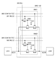
第1のスイッチSW11は、第1のトランジスタM11、第2のトランジスタM12、第3のトランジスタM13、第1の容量C11を有する。第1のトランジスタM11のソース又はドレインの一方は、第2のトランジスタM12のゲートと電気的に接続される。第1のトランジスタM11のソース又はドレインの一方は、第1の容量C11の一方の電極と電気的に接続される。第2のトランジスタM12のソース又はドレインの一方は、第3のトランジスタM13のソース又はドレインの一方と電気的に接続される。第1のトランジスタM11のゲートは、第1の信号線101と電気的に接続される。第1の信号線101から供給される信号を、WL[0]と表記する。WL[0]に基づいて、第1のトランジスタM11が選択される。第3のトランジスタM13のゲートは、第2の信号線102と電気的に接続される。第2の信号線102から供給される信号を、CONTEXT[0]と表記する。CONTEXT[0]に基づいて、第3のトランジスタM13が選択される。信号線とは、これら所望の信号を供給することができる配線である。
The first switch SW11 has a first transistor M11, a second transistor M12, a third transistor M13, and a first capacitor C11. One of a source and a drain of the first transistor M11 is electrically connected to a gate of the second transistor M12. One of a source and a drain of the first transistor M11 is electrically connected to one electrode of the first capacitor C11. One of a source and a drain of the second transistor M12 is electrically connected to one of a source and a drain of the third transistor M13. The gate of the first transistor M11 is electrically connected to the
第2のスイッチSW12は、第4のトランジスタM14、第5のトランジスタM15、第6のトランジスタM16、第2の容量C12を有する。第4のトランジスタM14のソース又はドレインの一方は、第5のトランジスタM15のゲートと電気的に接続される。第4のトランジスタM14のソース又はドレインの一方は、第2の容量C12の一方の電極と電気的に接続される。第5のトランジスタM15のソース又はドレインの一方は、第6のトランジスタM16のソース又はドレインの一方と電気的に接続される。第4のトランジスタM14のゲートは、第3の信号線103と電気的に接続される。第3の信号線103から供給される信号を、WL[1]と表記する。WL[1]に基づいて、第4のトランジスタM14が選択される。第6のトランジスタM16のゲートは、第4の信号線104と電気的に接続される。第4の信号線104から供給される信号を、CONTEXT[1]と表記する。CONTEXT[1]に基づいて、第6のトランジスタM16が選択される。信号線とは、これら所望の信号を供給することができる配線である。
The second switch SW12 has a fourth transistor M14, a fifth transistor M15, a sixth transistor M16, and a second capacitor C12. One of a source and a drain of the fourth transistor M14 is electrically connected to a gate of the fifth transistor M15. One of a source and a drain of the fourth transistor M14 is electrically connected to one electrode of the second capacitor C12. One of a source and a drain of the fifth transistor M15 is electrically connected to one of a source and a drain of the sixth transistor M16. The gate of the fourth transistor M14 is electrically connected to the
第1のトランジスタM11と、第4のトランジスタM14とは、互いのソース又はドレインの他方が電気的に接続されている。互いのソース又はドレインの他方は、第5の信号線105と電気的に接続されている。第5の信号線105から供給される信号を、BLと表記する。第1のトランジスタM11が選択されている場合、BLに基づいて、第1のトランジスタM11の先のノードSN11の電位を決めることができる。当該電位は、第1の容量C11によって、保持することができる。また第4のトランジスタM14が選択されている場合、BLに基づいて、第4のトランジスタM14の先のノードSN12の電位を決めることができる。当該電位は、第2の容量C12によって、保持することができる。信号線とは、所望の信号を供給することができる配線である。
The other of the source and the drain of the first transistor M11 and the fourth transistor M14 is electrically connected to each other. The other of the source and the drain is electrically connected to the
第2のトランジスタM12と、第5のトランジスタM15とは、互いのソース又はドレインの他方が電気的に接続されている。互いのソース又はドレインの他方は、LE11の出力側と電気的に接続されている。LE11の出力側の端子をノードND11と表記する。第3のトランジスタM13と、第6のトランジスタM16とは、互いのソース又はドレインの他方が、電気的に接続されている。互いのソース又はドレインの他方は、LE12の入力側と電気的に接続されている。LE12の入力側の端子をノードND12と表記する。 The other of the source and the drain of the second transistor M12 and the fifth transistor M15 are electrically connected to each other. The other of the source and the drain is electrically connected to the output side of the LE11. The terminal on the output side of LE11 is referred to as a node ND11. The other of the source and the drain of the third transistor M13 and the sixth transistor M16 are electrically connected to each other. The other of the source and the drain is electrically connected to the input side of the LE 12. A terminal on the input side of LE12 is referred to as a node ND12.
このような回路により、少なくとも、以下の動作を行うことができる。WL[0]により、第1のトランジスタM11の導通、非導通が制御される。WL[1]により、第4のトランジスタM14の導通、非導通が制御される。第1のトランジスタM11を介して、第1の容量C11に、BLに対応するコンフィギュレーションデータが書き込まれる。その後、第1のトランジスタM11が非導通となると、ノードSN11にコンフィギュレーションデータが格納される。 With such a circuit, at least the following operation can be performed. The conduction and non-conduction of the first transistor M11 is controlled by WL [0]. The conduction and non-conduction of the fourth transistor M14 is controlled by WL [1]. The configuration data corresponding to BL is written to the first capacitor C11 via the first transistor M11. Thereafter, when the first transistor M11 is turned off, the configuration data is stored in the node SN11.
第4のトランジスタM14を介して、第2の容量C12に、BLに対応するコンフィギュレーションデータが書き込まれる。その後、第4のトランジスタM14が非導通となると、ノードSN12にコンフィギュレーションデータが格納される。ノードSN11に格納されたコンフィギュレーションデータに依存して、第2のトランジスタM12の導通、非導通が制御される。ノードSN12に格納されたコンフィギュレーションデータに依存して、第5のトランジスタM15の導通、非導通が制御される。 The configuration data corresponding to BL is written to the second capacitor C12 via the fourth transistor M14. Thereafter, when the fourth transistor M14 is turned off, the configuration data is stored in the node SN12. The conduction and non-conduction of the second transistor M12 is controlled depending on the configuration data stored in the node SN11. The conduction and non-conduction of the fifth transistor M15 is controlled depending on the configuration data stored in the node SN12.
また、CONTEXT[0]により、第3のトランジスタM13の導通、非導通を制御することで、所望の回路構成を選択することができる。また、CONTEXT[1]により、第6のトランジスタM16の導通、非導通を制御することで、所望の回路構成を選択することができる。 Further, by controlling the conduction and non-conduction of the third transistor M13 by CONTEXT [0], a desired circuit configuration can be selected. Further, by controlling the conduction and non-conduction of the sixth transistor M16 with CONTEXT [1], a desired circuit configuration can be selected.
図11に、図10の回路におけるタイミングチャートを示す。図11は、第5の信号線105から供給されるBLのタイミングチャートを示す。図11は、第1の信号線101、第3の信号線103からそれぞれ供給されるWL[0],WL[1]のタイミングチャートを示す。図11は、第2の信号線102から供給されるCONTEXT[0]のタイミングチャートを示す。図11は、第4の信号線104から供給されるCONTEXT[1]のタイミングチャートを示す。
FIG. 11 shows a timing chart of the circuit of FIG. FIG. 11 shows a timing chart of the BL supplied from the
CONTEXT[0]が”H”レベルであり、CONTEXT[1]が”L”レベルの状態を第1のコンフィギュレーションデータを選択するとし、CONTEXT[0]が”L”レベルであり、CONTEXT[1]が”H”レベルの状態を第2のコンフィギュレーションデータを選択すると表記する。第1のコンフィギュレーションデータと、第2のコンフィギュレーションデータとは、いずれか一方しか選択できない。たとえば第1のコンフィギュレーションデータが選択されるときは、第2のコンフィギュレーションデータは非選択である。たとえば第2のコンフィギュレーションデータが選択されるときは、第1のコンフィギュレーションデータは非選択である。 When CONTEXT [0] is at “H” level and CONTEXT [1] is at “L” level to select the first configuration data, CONTEXT [0] is at “L” level and CONTEXT [1] ] Is “H” level when the second configuration data is selected. Only one of the first configuration data and the second configuration data can be selected. For example, when the first configuration data is selected, the second configuration data is not selected. For example, when the second configuration data is selected, the first configuration data is not selected.
図11において、トランジスタM11、トランジスタM12、トランジスタM13、トランジスタM14、トランジスタM15、トランジスタM16のゲートに印加した際、導通状態となる電位を”H”レベルとして表し、非導通状態となる電位を”L”レベルとして表す。”H”レベルの電位をVDDとし、”L”レベルの電位をGNDとするが、相対的な電位差があればよく、VDDやGNDに限定されるものではない。よって、第1の電位と、第1の電位より低い第2の電位や第1の電位と、第1の電位より高い第2の電位として、表現することができる。 In FIG. 11, when a voltage is applied to the gates of the transistor M11, the transistor M12, the transistor M13, the transistor M14, the transistor M15, and the transistor M16, the potential that is turned on is represented as “H” level, and the potential that is turned off is denoted as “L”. Expressed as "level." The “H” level potential is VDD and the “L” level potential is GND, but there is only a relative potential difference, and it is not limited to VDD or GND. Therefore, the first potential, the second potential lower than the first potential or the first potential, and the second potential higher than the first potential can be expressed.
図11において、ノードND11の電位が”L”レベルの間を時刻T0からT1とする。BLを”H”レベルとし、次いでWL[0]を”H”レベルとすることで、ノードSN11及び第1の容量C11を用いて、”H”レベルに相当するコンフィギュレーションデータを書き込むことができる。その後、WL[0]を”L”レベルとし、第1のトランジスタM11を非導通とすることで、ノードSN11及び第1の容量C11を用いて、コンフィギュレーションデータを格納することができる。WL[0]が”L”レベルとなった以降であれば、BLは”H”レベルであっても、”L”レベルであっても、第1のトランジスタM11を非導通とすることができる。ここでは、BLは、”L”レベルとする。 In FIG. 11, a period during which the potential of the node ND11 is at the “L” level is defined as time T0 to T1. By setting BL to “H” level and then setting WL [0] to “H” level, configuration data corresponding to “H” level can be written using the node SN11 and the first capacitor C11. . After that, by setting WL [0] to “L” level and turning off the first transistor M11, configuration data can be stored using the node SN11 and the first capacitor C11. After WL [0] goes to “L” level, the first transistor M11 can be turned off regardless of whether BL is at “H” level or “L” level. . Here, BL is at the “L” level.
時刻T1にて、第1のコンフィギュレーションデータを選択する。具体的には、CONTEXT[0]を”H”レベルとし、第3のトランジスタM13を導通させる。 At time T1, the first configuration data is selected. Specifically, CONTEXT [0] is set to the “H” level, and the third transistor M13 is turned on.
また、LE11側のノードND11を”L”レベルの電位から”H”レベルの電位へ変化させることで、第2のトランジスタM12のゲート容量を介した容量結合により、ノードSN11の電位は、たとえば約2VDDへ昇圧される。第2のトランジスタM12のソース・ゲート間電圧が約2VDDとなり、かつ第3のトランジスタM13は導通しているため、LE12側のノードND12の電位は、速やかに”H”レベルとなる。その結果、上記昇圧が行われない場合と比較して、ノードND11とノードND12間の信号伝達速度は向上する。 Further, by changing the potential of the node ND11 on the LE11 side from the “L” level potential to the “H” level potential, the potential of the node SN11 is reduced to, for example, approximately by the capacitive coupling via the gate capacitance of the second transistor M12. It is boosted to 2VDD. Since the voltage between the source and the gate of the second transistor M12 is about 2VDD and the third transistor M13 is conducting, the potential of the node ND12 on the LE12 side quickly becomes the "H" level. As a result, the signal transmission speed between the nodes ND11 and ND12 is improved as compared with the case where the boosting is not performed.
時刻T2にて、LE11側のノードND11を”H”レベルの電位から”L”レベルの電位へ変化させると、第2のトランジスタM12のゲート容量を介した容量結合により、ノードSN11の電位はVDDまで降圧される。第2のトランジスタM12のソース・ゲート間電圧がVDDとなり、かつ第3のトランジスタM13は導通しているため、GNDレベルの場合と比較して、ノードND12の電位は速やかに”L”レベルとなる。 At time T2, when the potential of the node ND11 on the LE11 side is changed from the “H” level potential to the “L” level potential, the potential of the node SN11 becomes VDD due to capacitive coupling via the gate capacitance of the second transistor M12. Step down to Since the voltage between the source and the gate of the second transistor M12 becomes VDD and the third transistor M13 is conductive, the potential of the node ND12 quickly becomes the "L" level as compared with the case of the GND level. .
図11からわかるように、第1のコンフィギュレーションデータを選択している間、ノードND11とノードND12間の信号伝達速度は向上し続ける。すなわち、一度、第2のトランジスタM12のゲート容量を介した容量結合により、ノードSN11の電位が昇圧又は降圧されれば、LE11とLE12間の信号伝達速度は向上し続ける。 As can be seen from FIG. 11, while the first configuration data is selected, the signal transmission speed between the nodes ND11 and ND12 continues to increase. That is, once the potential of the node SN11 is increased or decreased by capacitive coupling via the gate capacitance of the second transistor M12, the signal transmission speed between LE11 and LE12 continues to increase.
次にノードND11の電位が”L”レベルとなる間を時刻T3からT4とする。時刻T3からT4では、BLを”H”レベルとし、WL[1]を”H”レベルとすることで、ノードSN12及び第2の容量C12を用いて、”H”レベルに相当するコンフィギュレーションデータを書き込むことができる。その後、WL[1]を”L”レベルとし、第4のトランジスタM14を非導通とすることで、ノードSN12及び第2の容量C12を用いて、コンフィギュレーションデータを格納することができる。WL[1]が”L”レベルとなった以降であれば、BLは”H”レベルであっても、”L”レベルであっても、第4のトランジスタM14は非導通とすることができる。ここでは、BLは、”L”レベルとする。 Next, a period during which the potential of the node ND11 is at the “L” level is defined as time T3 to T4. From time T3 to T4, BL is set to the “H” level and WL [1] is set to the “H” level, so that the configuration data corresponding to the “H” level is obtained using the node SN12 and the second capacitor C12. Can be written. After that, by setting WL [1] to “L” level and turning off the fourth transistor M14, configuration data can be stored using the node SN12 and the second capacitor C12. After WL [1] goes to “L” level, the fourth transistor M14 can be turned off regardless of whether BL is at “H” level or “L” level. . Here, BL is at the “L” level.
時刻T4以降、第1のコンフィギュレーションデータを非選択にし、第2のコンフィギュレーションデータを選択する。具体的には、CONTEXT[0]を”L”レベルとし、第3のトランジスタM13を非導通にさせ、CONTEXT[1]を”H”レベルとし、第6のトランジスタM16を導通させる。 After time T4, the first configuration data is deselected and the second configuration data is selected. Specifically, CONTEXT [0] is set to “L” level, the third transistor M13 is turned off, CONTEXT [1] is set to “H” level, and the sixth transistor M16 is turned on.
また、LE11側のノードND11を”L”レベルの電位から”H”レベルの電位へ変化させることで、第5のトランジスタM15のゲート容量を介した容量結合により、ノードSN12の電位は、たとえば約2VDDへ昇圧される。第5のトランジスタM15のソース・ゲート間電圧が約2VDDとなり、かつ第6のトランジスタM16は導通しているため、LE12側のノードND12の電位は、速やかに”H”レベルとなる。その結果、上記昇圧が行われない場合と比較して、ノードND11とノードND12間の信号伝達速度が向上する。 Further, by changing the potential of the node ND11 on the LE11 side from the “L” level potential to the “H” level potential, the potential of the node SN12 is reduced to, for example, approximately by the capacitive coupling via the gate capacitance of the fifth transistor M15. It is boosted to 2VDD. Since the voltage between the source and the gate of the fifth transistor M15 becomes approximately 2VDD and the sixth transistor M16 is conducting, the potential of the node ND12 on the LE12 side quickly becomes the "H" level. As a result, the signal transmission speed between the nodes ND11 and ND12 is improved as compared with the case where the boosting is not performed.
時刻T5にて、LE11側のノードND11を”H”レベルの電位から”L”レベルの電位へ変化させると、第5のトランジスタM15のゲート容量を介した容量結合により、ノードSN12の電位はVDDまで降圧される。第5のトランジスタM15ソース・ゲート間電圧がVDDとなり、かつ第6のトランジスタM16は導通しているため、ノードND12の電位は速やかに”L”レベルとなる。 At time T5, when the potential of the node ND11 on the LE11 side is changed from the “H” level potential to the “L” level potential, the potential of the node SN12 becomes VDD due to capacitive coupling via the gate capacitance of the fifth transistor M15. Step down to Since the voltage between the source and the gate of the fifth transistor M15 becomes VDD and the sixth transistor M16 is conductive, the potential of the node ND12 quickly becomes the "L" level.
図11からわかるように、第2のコンフィギュレーションデータを選択している間、ノードND11とノードND12間の信号伝達速度は向上し続ける。すなわち、一度、第5のトランジスタM15のゲート容量を介した容量結合により、ノードSN12の電位が昇圧又は降圧されれば、LE11とLE12間の信号伝達速度は向上し続ける。 As can be seen from FIG. 11, while the second configuration data is selected, the signal transmission speed between the nodes ND11 and ND12 continues to increase. That is, once the potential of the node SN12 is increased or decreased by capacitive coupling via the gate capacitance of the fifth transistor M15, the signal transmission speed between LE11 and LE12 continues to increase.
図12を用いて、図11とは、別の条件を考える。 Using FIG. 12, another condition different from that in FIG. 11 is considered.
図12において、ノードND11の電位が”L”レベルの間を時刻T0’からT1’とする。図11と同様に考えることができ、時刻T0’からT1’では、ノードND11の電位が”L”レベルの間に、BLを”H”レベルとし、WL[0]を”H”レベルとすることで、第1の容量C11に”H”レベルに相当するコンフィギュレーションデータを書き込み、その後、WL[0]を”L”レベルとし、BLを”L”レベルとし、第1のトランジスタM11を非導通とすることで、ノードSN11のコンフィギュレーションデータを格納する。 In FIG. 12, a period during which the potential of the node ND11 is at the "L" level is defined as T1 'from T0'. It can be considered in the same manner as in FIG. 11, and from time T0 ′ to T1 ′, while the potential of the node ND11 is at the “L” level, BL is set to the “H” level and WL [0] is set to the “H” level. As a result, the configuration data corresponding to the “H” level is written to the first capacitor C11, after which WL [0] is set to the “L” level, BL is set to the “L” level, and the first transistor M11 is turned off. By making it conductive, the configuration data of the node SN11 is stored.
時刻T1’にて、第1のコンフィギュレーションデータを選択する。具体的には、CONTEXT[0]を”H”レベルとし、第3のトランジスタM13を導通させる。 At time T1 ', the first configuration data is selected. Specifically, CONTEXT [0] is set to the “H” level, and the third transistor M13 is turned on.
また、LE11側のノードND11を”L”レベルの電位から”H”レベルの電位へ変化させることで、第2のトランジスタM12のゲート容量を介した容量結合により、ノードSN11の電位は、たとえば約2VDDへ昇圧される。
その結果、図11と同様に、上記昇圧が行われない場合と比較して、ノードND11とノードND12間の信号伝達速度は向上する。
Further, by changing the potential of the node ND11 on the LE11 side from the “L” level potential to the “H” level potential, the potential of the node SN11 is reduced to, for example, approximately by the capacitive coupling via the gate capacitance of the second transistor M12. It is boosted to 2VDD.
As a result, as in FIG. 11, the signal transmission speed between the nodes ND11 and ND12 is improved as compared with the case where the boosting is not performed.
時刻T2’にて、LE11側のノードND11を”H”レベルの電位から”L”レベルの電位へ変化させることで、第2のトランジスタM12のゲート容量を介した容量結合により、ノードSN11の電位はVDDまで降圧される。第2のトランジスタM12のゲート・ソース間電圧がVDDとなるため、ノードND12の電位は速やかに”L”レベルとなる。 At the time T2 ′, the potential of the node SN11 is changed from the “H” level potential to the “L” level potential at the node ND11 on the LE11 side. Is reduced to VDD. Since the voltage between the gate and the source of the second transistor M12 becomes VDD, the potential of the node ND12 quickly becomes the "L" level.
次にノードND11の電位が”H”レベルとなっている時刻T3’からT4’とする。時刻T3’からT4’では、ノードND11の電位が”H”レベルの間に、BLを”H”レベルとし、WL[1]を”H”レベルとすることで、ノードSN12及び第2の容量C12を用いて、”H”レベルに相当するコンフィギュレーションデータを書き込むことができる。その後、WL[1]を”L”レベルとし、第4のトランジスタM14を非導通とすることで、ノードSN12及び第2の容量C12を用いて、コンフィギュレーションデータを格納することができる。 Next, it is assumed that the potential of the node ND11 is at "H" level from time T3 'to T4'. From the time T3 'to T4', while the potential of the node ND11 is at the "H" level, the BL is set to the "H" level and the WL [1] is set to the "H" level, thereby setting the node SN12 and the second capacitor. Using C12, configuration data corresponding to the “H” level can be written. After that, by setting WL [1] to “L” level and turning off the fourth transistor M14, configuration data can be stored using the node SN12 and the second capacitor C12.
時刻T4’以降、第1のコンフィギュレーションデータを非選択にし、第2のコンフィギュレーションデータを選択する。具体的には、CONTEXT[0]を”L”レベルとし、第3のトランジスタM13を非導通にさせ、CONTEXT[1]を”H” レベルとし、第6のトランジスタM16を導通させる。 After time T4 ', the first configuration data is deselected and the second configuration data is selected. Specifically, CONTEXT [0] is set to “L” level, the third transistor M13 is turned off, CONTEXT [1] is set to “H” level, and the sixth transistor M16 is turned on.
このとき、LE11側のノードND11が”H”レベルの状態で、上記時刻T4’の動作を迎えてしまうと、その後、LE11側のノードND11が”H”レベルの電位から”L”レベルの電位へ変化することとなる。この場合、ノードSN12の電位は昇圧されず、第5のトランジスタM15のゲート容量を介した容量結合により、ノードSN12の電位はVDDより小さく、GND近くまで降圧されてしまう。 At this time, if the operation at the time T4 ′ is reached while the node ND11 on the LE11 side is at the “H” level, then the potential of the node ND11 on the LE11 side is changed from the “H” level potential to the “L” level potential. Will change to In this case, the potential of the node SN12 is not boosted, and the potential of the node SN12 is lower than VDD and drops to near GND due to capacitive coupling via the gate capacitance of the fifth transistor M15.
時刻T5’にて、LE11側のノードND11を”L”レベルの電位から”H”レベルの電位へ変化させる。ノードSN12の電位は、時刻T4’に降圧され、VDDよりも小さな値となったままであり、第5のトランジスタM15の駆動能力は小さくなる。このように、ノードND11とノードND12間の信号伝達速度が低下してしまう場合がある。 At time T5 ', the potential of the node ND11 on the LE11 side is changed from the "L" level potential to the "H" level potential. The potential of the node SN12 is stepped down at time T4 ', remains at a value smaller than VDD, and the driving capability of the fifth transistor M15 decreases. Thus, the signal transmission speed between the nodes ND11 and ND12 may be reduced.
また、ノードSN12の電位の降圧幅が大きい場合、ノードSN12の電位は”H”レベルから”L”レベルに変化することもある。この場合、ノードND11とノードND12間において、正しい論理信号が伝達されないことさえ懸念される。 Further, when the step-down width of the potential of the node SN12 is large, the potential of the node SN12 may change from “H” level to “L” level. In this case, there is a concern that a correct logic signal is not transmitted between node ND11 and node ND12.
以上より、選択されたコンフィギュレーションデータに対応した動作時に、非選択のコンフィギュレーションデータを書き換えるマルチコンテキスト方式の場合、ノードND11の電位に依存して、ノードND11とノードND12間の信号伝達速度が低下する場合があった。 As described above, in the case of the multi-context method in which the non-selected configuration data is rewritten during the operation corresponding to the selected configuration data, the signal transmission speed between the nodes ND11 and ND12 decreases depending on the potential of the node ND11. There was a case.
本発明の一態様は少なくとも上述した新たな一課題を認識し、当該一課題を解決するために、LEの出力電位を”L”レベルとする回路構成及びその駆動方法を提案する。または、本発明の一態様は新規な回路を提案する。または、本発明の一態様は新規な回路の駆動方法を提案する。または、本発明の一態様は新規な半導体装置を提案する。なお、これらの課題の記載は、他の課題の存在を妨げるものではない。なお、本発明の一態様は、必ずしも、これらの課題の全てを解決する必要はない。なお、これら以外の課題は、明細書、図面、請求項などの記載から、自ずと明らかとなるものであり、明細書、図面、請求項などの記載から、これら以外の課題を抽出することが可能である。 One embodiment of the present invention recognizes at least the new problem described above, and proposes a circuit configuration in which the output potential of the LE is set to an “L” level and a driving method thereof in order to solve the problem. Alternatively, one embodiment of the present invention proposes a novel circuit. Alternatively, one embodiment of the present invention proposes a novel circuit driving method. Alternatively, one embodiment of the present invention proposes a novel semiconductor device. Note that the description of these objects does not disturb the existence of other objects. Note that one embodiment of the present invention does not necessarily need to solve all of these problems. It should be noted that issues other than these are obvious from the description of the specification, drawings, claims, etc., and that other issues can be extracted from the description of the description, drawings, claims, etc. It is.
本発明の一態様は、第1のロジックエレメントと、記第1のロジックエレメントと電気的に接続された第1のスイッチと、記第1のスイッチと電気的に接続された第2のロジックエレメントと、を有し、少なくとも、第1のロジックエレメントは、第2のスイッチを有し、第2のスイッチは、第1のロジックエレメントからの出力電位をLレベルとする機能を有する半導体装置である。 One embodiment of the present invention provides a first logic element, a first switch electrically connected to the first logic element, and a second logic element electrically connected to the first switch. Wherein at least the first logic element includes a second switch, and the second switch is a semiconductor device having a function of setting an output potential from the first logic element to an L level. .
本発明の一態様は、第1のロジックエレメントと、第1のロジックエレメントと電気的に接続された第1のスイッチと、第1のスイッチと電気的に接続された第2のロジックエレメントと、を有し、少なくとも、第1のロジックエレメントは、論理積回路を有し、論理積回路は、前記第1のロジックエレメントからの出力電位をLレベルとする機能を有する半導体装置である。 One embodiment of the present invention includes a first logic element, a first switch electrically connected to the first logic element, a second logic element electrically connected to the first switch, And at least the first logic element has an AND circuit, and the AND circuit is a semiconductor device having a function of setting an output potential from the first logic element to an L level.
本発明の一態様は、第1のロジックエレメントと、第1のロジックエレメントと電気的に接続された第1のスイッチと、第1のスイッチと電気的に接続された第2のロジックエレメントと、を有し、少なくとも、第1のロジックエレメントは、AND回路を有し、AND回路は、第1のロジックエレメントからの出力電位をLレベルとする機能を有する半導体装置である。 One embodiment of the present invention includes a first logic element, a first switch electrically connected to the first logic element, a second logic element electrically connected to the first switch, And at least the first logic element has an AND circuit, and the AND circuit is a semiconductor device having a function of setting an output potential from the first logic element to an L level.
本発明の一態様において、第1のスイッチは、第1のトランジスタと、第2のトランジスタと、第3のトランジスタと、容量とを有し、第2のトランジスタのゲートは、第1のトランジスタのソース又はドレインの一方と電気的に接続され、第2のトランジスタのゲートは、容量の第1の電極と電気的に接続され、第1のトランジスタのゲートは、第1の信号線と電気的に接続され、第3のトランジスタのゲートは、第2の信号線と電気的に接続され、第2の信号線からの信号に基づき、複数のコンテキストのうち、いずれか一を選択する機能を有することができる。 In one embodiment of the present invention, the first switch has a first transistor, a second transistor, a third transistor, and a capacitor, and a gate of the second transistor is connected to the first transistor. The transistor is electrically connected to one of a source and a drain, a gate of the second transistor is electrically connected to a first electrode of the capacitor, and a gate of the first transistor is electrically connected to a first signal line. Connected, a gate of the third transistor is electrically connected to the second signal line, and has a function of selecting one of a plurality of contexts based on a signal from the second signal line. Can be.
本発明の一態様において、第1のトランジスタは、酸化物半導体層を有することができ、第2のトランジスタは、酸化物半導体層を有することができる。 In one embodiment of the present invention, the first transistor can include an oxide semiconductor layer, and the second transistor can include an oxide semiconductor layer.
本発明の一態様は、第1のロジックエレメントと、第1のロジックエレメントと電気的に接続された、スイッチと、スイッチと電気的に接続された、第2のロジックエレメントとを有し、少なくとも、第1のロジックエレメントは、レジスタと電気的に接続されたメモリを有し、メモリは、レジスタのデータを保持する機能を有し、レジスタは、メモリにデータを保持したあと、出力電位をLレベルとする機能を有する半導体装置である。 One embodiment of the present invention includes a first logic element, a switch electrically connected to the first logic element, and a second logic element electrically connected to the switch, at least , The first logic element has a memory electrically connected to the register, and the memory has a function of holding the data of the register. The register holds the data in the memory and then changes the output potential to L. It is a semiconductor device having a function of level.
本発明の一態様において、メモリは、酸化物半導体層を有するトランジスタを有することができる。 In one embodiment of the present invention, the memory can include a transistor including an oxide semiconductor layer.
本発明の一態様によれば、コンフィギュレーションを行う際に、容量結合による電荷保持ノードの昇圧効果を用いて、信号伝達速度が向上した半導体装置及びその駆動方法を提供することができる。 According to one embodiment of the present invention, it is possible to provide a semiconductor device in which signal transmission speed is improved by using a boosting effect of a charge holding node due to capacitive coupling during configuration and a driving method thereof.
本発明の一態様によれば、上記信号伝達速度を低下させることのない半導体装置及びその駆動方法を提供することができる。または、本発明の一態様によれば、新規な半導体装置を提供することができる。または、本発明の一態様によれば、新規な半導体装置の駆動方法を提供することができる。なお、これらの効果の記載は、他の効果の存在を妨げるものではない。なお、本発明の一態様は、必ずしも、これらの効果の全てを有する必要はない。なお、これら以外の効果は、明細書、図面、請求項などの記載から、自ずと明らかとなるものであり、明細書、図面、請求項などの記載から、これら以外の効果を抽出することが可能である。 According to one embodiment of the present invention, a semiconductor device which does not reduce the signal transmission speed and a driving method thereof can be provided. Alternatively, according to one embodiment of the present invention, a novel semiconductor device can be provided. Alternatively, according to one embodiment of the present invention, a novel method for driving a semiconductor device can be provided. Note that the description of these effects does not disturb the existence of other effects. Note that one embodiment of the present invention does not necessarily need to have all of these effects. It should be noted that effects other than these are obvious from the description of the specification, drawings, claims, and the like, and other effects can be extracted from the description of the specification, drawings, claims, and the like. It is.
実施の形態について、図面を用いて詳細に説明する。但し、本発明は以下の説明に限定されず、本発明の趣旨及びその範囲から逸脱することなくその形態及び詳細を様々に変更し得ることは当業者であれば容易に理解される。従って、本発明は以下に示す実施の形態の記載内容に限定して解釈されるものではない。なお、以下に説明する発明の構成において、同一部分又は同様な機能を有する部分には同一の符号を異なる図面間で共通して用い、その繰り返しの説明は省略する。 Embodiments will be described in detail with reference to the drawings. However, the present invention is not limited to the following description, and it is easily understood by those skilled in the art that the form and details can be variously changed without departing from the spirit and scope of the present invention. Therefore, the present invention is not construed as being limited to the description of the embodiments below. Note that in the structures of the invention described below, the same portions or portions having similar functions are denoted by the same reference numerals in different drawings, and description thereof is not repeated.
ここで、先に説明した図11のタイミングチャートと、図12のタイミングチャートとの違いから、本発明者等は、ノードND11とノードND12間の信号伝達速度が向上するためには、少なくとも、コンフィギュレーションデータを書き込む際(図11の時刻T4、図12の時刻T4’)に、LE11の出力電位であるノードND11の電位が”L”レベルとなっていることが好ましいことを見出した。 Here, from the difference between the timing chart of FIG. 11 described above and the timing chart of FIG. 12, the present inventors require at least the configuration chart to improve the signal transmission speed between the nodes ND11 and ND12. It has been found that when writing the application data (time T4 in FIG. 11 and time T4 ′ in FIG. 12), it is preferable that the potential of the node ND11 which is the output potential of the LE11 be at the “L” level.
(実施の形態1)
本実施の形態では、コンフィギュレーションデータを書き込む際に、LEの出力電位が”L”レベルとなる半導体装置の一構成について説明する。
(Embodiment 1)
In this embodiment, one configuration of a semiconductor device in which the output potential of the LE is set to the “L” level when writing configuration data is described.
図1に、本発明の一態様におけるPLDの回路構成を示す。図1に示すように、複数のLE(LE21、LE22、・・・、LE2n)、複数のスイッチ(SW21−21、SW21−22、・・・、SW21−2n、SW22−21、SW22−22、・・・、SW22−2n、・・・、SW2n−21、SW2n−22、・・・、SW2n−2n)、第1のドライバ、第2のドライバを有する。第1のドライバは、ビットドライバ(BD2)として機能する。第2のドライバは、ワードドライバ(WD2)として機能する。複数のSWはそれぞれ、複数のLE間を電気的に接続している。 FIG. 1 illustrates a circuit configuration of a PLD according to one embodiment of the present invention. As shown in FIG. 1, a plurality of LEs (LE21, LE22,..., LE2n), a plurality of switches (SW21-21, SW21-22,..., SW21-2n, SW22-21, SW22-22, , SW22-2n, ..., SW2n-21, SW2n-22, ..., SW2n-2n), a first driver, and a second driver. The first driver functions as a bit driver (BD2). The second driver functions as a word driver (WD2). Each of the plurality of SWs electrically connects the plurality of LEs.
LEは内部にコンフィギュレーションメモリを有する。当該コンフィギュレーションメモリに格納されたコンフィギュレーションデータに基づき、入力された信号に応じて、特定の出力信号を出力する機能を有する。 The LE has a configuration memory inside. A function of outputting a specific output signal in accordance with an input signal based on the configuration data stored in the configuration memory;
複数のSWは、複数のLE間の導通状態(オンとオフ)を制御する機能を有する。図1では、LE21と電気的に接続されるSWは、少なくともSW21−21、SW22−21・・・SW2n−21、SW21−22、・・・SW21−2nがある。SW21−21、SW22−21・・・SW2n−21は、少なくとも、LE21の入力側と電気的に接続されている。SW21−21、SW21−22、・・・SW21−2nは、少なくともLE21の入力側及び出力側に電気的に接続されている。図1のような回路構成のため、SWは、LEよりも多く配置される。
The plurality of SWs have a function of controlling a conduction state (on and off) between the plurality of LEs. In FIG. 1, the SWs electrically connected to the
図1において、LE21への入力は1端子で説明されるが、入力の端子は複数あってもよく、4つの入力端子を配置することができる。この場合、LE21と電気的に接続されるスイッチの数が、図1で示された回路構成よりも増加することとなる。
In FIG. 1, the input to the
ビットドライバ(BD2)、ワードドライバ(WD2)は、LE及びSWのコンフィギュレーションを制御する機能を有する。ワードドライバ(WD2)は、WLを出力する機能、当該WLを出力する信号線を選択する機能を有する。ビットドライバ(BD2)、ワードドライバ(WD2)以外に、コントローラ等を有する。 The bit driver (BD2) and the word driver (WD2) have a function of controlling LE and SW configurations. The word driver (WD2) has a function of outputting a WL and a function of selecting a signal line that outputs the WL. A controller and the like are provided in addition to the bit driver (BD2) and the word driver (WD2).
コンフィギュレーションが行なわれる複数のSWは、WLによって選択される。図1に示す回路構成において、コンフィギュレーションが行なわれるSWは、2種類の信号(WL[0]、WL[1])によって選択される。選択されたSWは、BLの電位に依存したコンフィギュレーションデータによりコンフィギュレーションが行われる。具体的に、SW21−22を用いて説明すると、SW21−22は2種類の信号(WL22[0]、WL22[1])に基づいて選択され、選択されたとき、BL21の電位に依存したコンフィギュレーションデータにより、コンフィギュレーションが行われる。 A plurality of SWs on which configuration is performed are selected by WL. In the circuit configuration shown in FIG. 1, the SW to be configured is selected by two types of signals (WL [0] and WL [1]). The selected SW is configured by configuration data depending on the potential of BL. More specifically, using SW21-22, SW21-22 is selected based on two types of signals (WL22 [0], WL22 [1]), and when selected, a configuration dependent on the potential of BL21. Configuration is performed according to the configuration data.
図2では、図1の2つのLEとその間の1つのSWについて、より具体的に説明する。2つのLEをそれぞれ、LE21,LE22とする。LE21と,LE22との間にある、スイッチをSW21−22と示す。 In FIG. 2, the two LEs in FIG. 1 and one SW therebetween are described more specifically. The two LEs are referred to as LE21 and LE22, respectively. The switch between LE21 and LE22 is indicated as SW21-22.
本発明の一態様のLEは、少なくともスイッチを有することが特徴となる。図2では、LE21にスイッチ201を設けた場合で説明するが、LE22にも同様なスイッチを設けることができる。図1で示されたLEにも、同様なスイッチを設けることができる。
The LE of one embodiment of the present invention is characterized by having at least a switch. FIG. 2 illustrates the case where the
上記スイッチ201は論理積回路を有する。論理積回路は、2個以上の入力端子と、1個の出力端子を有する。すべての入力端子に入力1が入る場合にだけ、出力端子に出力1が出力され、それ以外の場合は0を出力することができる回路である。論理積回路には、たとえばAND回路を用いることができる。
The
スイッチ201は、コントローラから出力された信号(SWITCH)によって制御される。SWITCHは、第11の信号線211からスイッチ201へ入力される。レジスタ203の出力信号が”H”レベルであっても、SWITCHを”L”レベルとすることで、スイッチ201からは、”L”レベルの信号が出力されることになる。
The
上記したように、少なくとも、スイッチ201を有することで、LE21からの信号を、”L”レベルとすることができる。
As described above, by providing at least the
レジスタ203は、ルックアップテーブル(以下、LUT)202からの出力信号を保持し、第10の信号線210からの信号(クロック信号であって、以下CLKと記す)に同期して、対応する出力値を出力する機能を有する。
The
LUT202と、レジスタ203との間を、ノードND21とする。レジスタ203と、スイッチ201との間を、ノードND22とする。
The node between the
その他、LE21は、記憶装置204を有する。記憶装置204が有するコンフィギュレーションデータに従って、LUT202では、実行される論理演算が定義される。LUT202は、複数の入力信号に対して、定められた一つの出力信号を出力する。
In addition, the
記憶装置204は、第2の信号線102及び第4の信号線104と電気的に接続される。第2の信号線102には、第1のコンフィギュレーションデータを選択するための信号CONTEXT[0]が供給される。第4の信号線104には、第2のコンフィギュレーションデータを選択するための信号CONTEXT[1]が供給される。CONTEXT[0]やCONTEXT[1]は、コントローラから出力される。
The
CONTEXT[0]が”H”レベルであり、CONTEXT[1]が”L”レベルの状態を第1のコンフィギュレーションデータを選択するとし、CONTEXT[0]が”L”レベルであり、CONTEXT[1]が”H”レベルの状態を第2のコンフィギュレーションデータを選択すると表記する。第1のコンフィギュレーションデータと、第2のコンフィギュレーションデータとは、いずれか一方しか選択できない。たとえば第1のコンフィギュレーションデータが選択されるときは、第2のコンフィギュレーションデータは非選択である。たとえば第2のコンフィギュレーションデータが選択されるときは、第1のコンフィギュレーションデータは非選択である。 When CONTEXT [0] is at “H” level and CONTEXT [1] is at “L” level to select the first configuration data, CONTEXT [0] is at “L” level and CONTEXT [1] ] Is “H” level when the second configuration data is selected. Only one of the first configuration data and the second configuration data can be selected. For example, when the first configuration data is selected, the second configuration data is not selected. For example, when the second configuration data is selected, the first configuration data is not selected.
第1のコンフィギュレーションデータ及び第2のコンフィギュレーションデータのうち、どちらか一方を選択することで、所望の回路構成を得ることができる。また、選択したコンフィギュレーションデータに対応した回路動作時に、非選択のコンフィギュレーションデータを変更することができる。すなわち、半導体装置はマルチコンテキスト機能を有する。 By selecting one of the first configuration data and the second configuration data, a desired circuit configuration can be obtained. Further, at the time of the circuit operation corresponding to the selected configuration data, the non-selected configuration data can be changed. That is, the semiconductor device has a multi-context function.
本実施の形態において、コンフィギュレーションデータを選択する際の電位を”H”レベルとして表し、非選択する際の電位を”L”レベルとして表す。”H”レベルの電位をVDDとし、”L”レベルの電位をGNDとするが、相対的な電位差があればよく、VDDやGNDに限定されるものではない。 In the present embodiment, the potential when selecting the configuration data is represented as “H” level, and the potential when not selecting is represented as “L” level. The “H” level potential is VDD and the “L” level potential is GND, but there is only a relative potential difference, and it is not limited to VDD or GND.
LE22は、上記したLE21と同じ構成を有することができる。LE22もスイッチ201を有することができる。
LE22 can have the same configuration as LE21 described above.
LE21とLE22との間には、スイッチSW21−22が設けられている。スイッチSW21−22は、第2の信号線102及び第4の信号線104と電気的に接続されている。
A switch SW21-22 is provided between LE21 and LE22. The switches SW21-22 are electrically connected to the
LE21と、スイッチSW21−22と間を、ノードND23とする。スイッチSW21−22と、LE22と間を、ノードND24とする。
A node between the
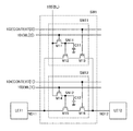
図3に、スイッチSW21−22の回路構成を例示す。スイッチSW21−22は、第1のスイッチSW21及び第2のスイッチSW22を有する。スイッチSW21−22は、複数のスイッチを有することができ、スイッチ群と呼ぶことができる。第1のスイッチSW21は、LE21及びLE22間の導通、非導通を制御する機能を有する。第2のスイッチSW22は、第1のスイッチSW21と同様な構成及び機能を有することができる。これらスイッチについて説明する。 FIG. 3 shows an example of a circuit configuration of the switches SW21-22. The switches SW21-22 include a first switch SW21 and a second switch SW22. The switches SW21-22 can have a plurality of switches, and can be called a switch group. The first switch SW21 has a function of controlling conduction and non-conduction between LE21 and LE22. The second switch SW22 can have a configuration and a function similar to those of the first switch SW21. These switches will be described.
第1のスイッチSW21は、第1のトランジスタM21、第2のトランジスタM22、第3のトランジスタM23、第1の容量C21を有する。第1のトランジスタM21のソース又はドレインの一方は、第2のトランジスタM22のゲートと電気的に接続される。第1のトランジスタM21のソース又はドレインの一方は、第1の容量C21の一方の電極と電気的に接続される。第2のトランジスタM22のソース又はドレインの一方は、第3のトランジスタM23のソース又はドレインの一方と電気的に接続される。第1のトランジスタM21のゲートは、第1の信号線301と電気的に接続される。第1の信号線301から供給される信号を、WL[0]と表記する。WL[0]に基づいて、第1のトランジスタM21が選択される。第3のトランジスタM23のゲートは、第2の信号線302と電気的に接続される。第2の信号線302から供給される信号を、CONTEXT[0]と表記する。CONTEXT[0]に基づいて、第3のトランジスタM23が選択される。信号線とは、これら所望の信号を供給することができる配線である。
The first switch SW21 has a first transistor M21, a second transistor M22, a third transistor M23, and a first capacitor C21. One of a source and a drain of the first transistor M21 is electrically connected to a gate of the second transistor M22. One of a source and a drain of the first transistor M21 is electrically connected to one electrode of the first capacitor C21. One of a source and a drain of the second transistor M22 is electrically connected to one of a source and a drain of the third transistor M23. The gate of the first transistor M21 is electrically connected to the
第2のスイッチSW22は、第4のトランジスタM24、第5のトランジスタM25、第6のトランジスタM26、第2の容量C22を有する。第4のトランジスタM24のソース又はドレインの一方は、第5のトランジスタM25のゲートと電気的に接続される。第4のトランジスタM24のソース又はドレインの一方は、第2の容量C22の一方の電極と電気的に接続される。第5のトランジスタM25のソース又はドレインの一方は、第6のトランジスタM26のソース又はドレインの一方と電気的に接続される。第4のトランジスタM24のゲートは、第3の信号線303と電気的に接続される。第3の信号線303から供給される信号を、WL[1]と表記する。第6のトランジスタM26のゲートは、第4の信号線304と電気的に接続される。第4の信号線304から供給される信号を、CONTEXT[1]と表記する。信号線とは、これら所望の信号を供給することができる配線である。
The second switch SW22 has a fourth transistor M24, a fifth transistor M25, a sixth transistor M26, and a second capacitor C22. One of a source and a drain of the fourth transistor M24 is electrically connected to a gate of the fifth transistor M25. One of a source and a drain of the fourth transistor M24 is electrically connected to one electrode of the second capacitor C22. One of a source and a drain of the fifth transistor M25 is electrically connected to one of a source and a drain of the sixth transistor M26. The gate of the fourth transistor M24 is electrically connected to the
第1のトランジスタM21と、第4のトランジスタM24とは、互いのソース又はドレインの他方が電気的に接続されている。互いのソース又はドレインの他方は、第5の信号線305と電気的に接続されている。第5の信号線305から供給される信号を、BLと表記する。第1のトランジスタM21が選択されている場合、BLに基づいて、第1のトランジスタM21の先のノードSN21の電位を決めることができる。当該電位は、第1の容量C21によって、保持することができる。また第4のトランジスタM24が選択されている場合、BLに基づいて、第4のトランジスタM24の先のノードSN22の電位を決めることができる。当該電位は、第2の容量C22によって、保持することができる。信号線とは、所望の信号を供給することができる配線である。
The other of the source and the drain of the first transistor M21 and the fourth transistor M24 is electrically connected to each other. The other of the source and the drain is electrically connected to the
第2のトランジスタM22と、第5のトランジスタM25とは、互いのソース又はドレインの他方が電気的に接続されている。互いのソース又はドレインの他方は、LE21の出力側と電気的に接続されている。LE21の出力側の端子をノードND23と表記する。第3のトランジスタM23と、第6のトランジスタM26とは、互いのソース又はドレインの他方が、電気的に接続されている。互いのソース又はドレインの他方は、LE22の入力側と電気的に接続されている。LE22の入力側の端子をノードND24と表記する。
The other of the source and the drain of the second transistor M22 and the fifth transistor M25 are electrically connected to each other. The other of the source and the drain is electrically connected to the output side of the
このような回路により、少なくとも、以下の動作を行うことができる。WL[0]により、第1のトランジスタM21の導通、非導通を制御することができ、ノードSN21及び第1の容量C21を用いて、第5の信号線305から供給される信号に対応するコンフィギュレーションデータを書き込むことができる。ノードSN21に格納されたコンフィギュレーションデータに依存して、第2のトランジスタM22の導通、非導通が制御される。また、CONTEXT[0]により、第3のトランジスタM23の導通、非導通を制御することで、所望の回路構成を選択することができる。
With such a circuit, at least the following operation can be performed. The conduction and non-conduction of the first transistor M21 can be controlled by WL [0], and the configuration corresponding to the signal supplied from the
WL[1]により、第4のトランジスタM24の導通、非導通を制御し、ノードSN22および第2の容量C22を用いて、BLに対応するコンフィギュレーションデータを書き込むことができる。ノードSN22に格納されたコンフィギュレーションデータに依存して、第5のトランジスタM25の導通、非導通が制御される。また、CONTEXT[1]、第6のトランジスタM26の導通、非導通を制御することで、所望の回路構成を選択することができる。 By WL [1], conduction and non-conduction of the fourth transistor M24 can be controlled, and configuration data corresponding to BL can be written using the node SN22 and the second capacitor C22. The conduction and non-conduction of the fifth transistor M25 is controlled depending on the configuration data stored in the node SN22. Further, a desired circuit configuration can be selected by controlling the conduction and non-conduction of the CONTEXT [1] and the sixth transistor M26.
図4に図3の回路におけるタイミングチャートを示す。ここで、LUT202の出力値としてノードND21のような出力波形が出力されるとする。また、”H”レベルに相当する電位をVDD、”L”レベルに相当する電位をGNDとする場合で説明するが、相対的な電位差があればよく、VDDやGNDに限定されるものではない。よって、第1の電位と、第1の電位より低い第2の電位や第1の電位と、第1の電位より高い第2の電位として、表現することができる。
FIG. 4 shows a timing chart of the circuit of FIG. Here, it is assumed that the output waveform of the node ND21 is output as the output value of the
時刻T0からT1の間、すなわちノードND23の電位が”L”レベルの間に、BLを、”H”レベルとし、WL[0]を”H”レベルとすることで、ノードSN21及び第1の容量C21を用いて、”H”レベルに相当するコンフィギュレーションデータを書き込むことができる。その後、WL[0]を”L”レベルとし、BLを”L”レベルとし、第1のトランジスタM21を非導通とすることで、ノードSN21及び第1の容量C21を用いて、コンフィギュレーションデータを格納することができる。コンフィギュレーションデータは一定期間格納される必要があるため、オフ電流が非常に小さい、酸化物半導体を有するトランジスタを、第1のトランジスタM21に適用するとよい。酸化物半導体を有するトランジスタのオフ電流は非常に小さいものであるため、第1の容量C21は設けなくともよいと考えることもできる。 Between the time T0 and T1, that is, while the potential of the node ND23 is at the "L" level, the BL is set to the "H" level and the WL [0] is set to the "H" level, thereby setting the node SN21 and the first Using the capacitor C21, configuration data corresponding to the “H” level can be written. After that, the WL [0] is set to the “L” level, the BL is set to the “L” level, and the first transistor M21 is turned off, so that the configuration data is transferred using the node SN21 and the first capacitor C21. Can be stored. Since the configuration data needs to be stored for a certain period, a transistor including an oxide semiconductor with extremely low off-state current may be used as the first transistor M21. Since the off-state current of the transistor including an oxide semiconductor is extremely small, it can be considered that the first capacitor C21 does not need to be provided.
なお、WL[0]が”L”レベルとなった以降であれば、BLは”H”レベルであっても、”L”レベルであっても、第1のトランジスタM21を非導通とすることができる。 Note that after the WL [0] becomes “L” level, the first transistor M21 is turned off regardless of whether BL is at “H” level or “L” level. Can be.
時刻T1にて、第1のコンフィギュレーションデータを選択する。具体的には、CONTEXT[0]を”H”レベルとし、第3のトランジスタM23を導通させる。 At time T1, the first configuration data is selected. Specifically, CONTEXT [0] is set to the “H” level, and the third transistor M23 is turned on.
また、LE21側のノードND23を”L”レベルの電位から”H”レベルの電位へ変化させることで、第2のトランジスタM22のゲート容量を介した容量結合により、ノードSN21の電位は、たとえば約2VDDにまで昇圧される。第2のトランジスタM22のソース・ゲート間電圧が約2VDDとなり、かつ第3のトランジスタM23は導通しているため、LE22側のノードND24の電位は、速やかに”H”レベルとなる。その結果、上記昇圧が行われない場合と比較して、ノードND23とノードND24間の信号伝達速度は向上する。 Further, by changing the potential of the node ND23 on the side of the LE21 from the “L” level potential to the “H” level potential, the potential of the node SN21 becomes, for example, approximately by the capacitive coupling via the gate capacitance of the second transistor M22. The voltage is boosted to 2VDD. Since the source-gate voltage of the second transistor M22 is about 2 VDD and the third transistor M23 is conductive, the potential of the node ND24 on the LE22 side quickly goes to the "H" level. As a result, the signal transmission speed between the nodes ND23 and ND24 is improved as compared with the case where the boosting is not performed.
ノードSN21の昇圧幅は、第1の容量C21の容量値が小さいほど、大きくなる。その結果、信号伝達速度がより向上する。酸化物半導体を用いて第1のトランジスタM21を構成する場合、第1の容量C21の容量値はシリコン半導体を用いて構成した場合より、小さくすることができ、好ましい。 The boost width of the node SN21 increases as the capacitance value of the first capacitor C21 decreases. As a result, the signal transmission speed is further improved. In the case where the first transistor M21 is formed using an oxide semiconductor, the capacitance of the first capacitor C21 can be smaller than that in a case where the first transistor M21 is formed using a silicon semiconductor, which is preferable.
第2のトランジスタM22は、酸化物半導体を有するトランジスタやシリコンを有するトランジスタ等、どのようなトランジスタを用いてもよい。第2のトランジスタM22のソース・ゲート間電圧を昇圧させることができるため、たとえば、シリコンを有するトランジスタより、オン電流が小さいとされる酸化物半導体を有するトランジスタを適用しても、信号伝達速度を向上させることができるため、好ましい。 As the second transistor M22, any transistor such as a transistor including an oxide semiconductor or a transistor including silicon may be used. Since the source-gate voltage of the second transistor M22 can be increased, the signal transmission speed can be reduced even when a transistor including an oxide semiconductor whose on-state current is assumed to be smaller than that of a transistor including silicon is used, for example. It is preferable because it can be improved.
時刻T2にて、LE21側のノードND23を”H”レベルの電位から”L”レベルの電位へ変化させると、第2のトランジスタM22のゲート容量を介した容量結合により、ノードSN21の電位はVDDまで降圧される。第2のトランジスタM22のゲート・ソース間電圧がVDDとなり、かつ第3のトランジスタM23は導通しているため、GNDレベルの場合と比較して、ノードND24の電位は速やかに”L”レベルとなる。 At time T2, when the potential of the node ND23 on the LE21 side is changed from the “H” level potential to the “L” level potential, the potential of the node SN21 becomes VDD due to capacitive coupling via the gate capacitance of the second transistor M22. Step down to Since the gate-source voltage of the second transistor M22 becomes VDD and the third transistor M23 is conductive, the potential of the node ND24 becomes the "L" level more quickly than in the case of the GND level. .
図4からわかるように、第1のコンフィギュレーションデータを選択している間、ノードND23とノードND24間の信号伝達速度は向上し続ける。すなわち、一度、第2のトランジスタM22のゲート容量を介した容量結合により、ノードSN21の電位が昇圧又は降圧されれば、LE21とLE22間の信号伝達速度は向上し続けることとなる。 As can be seen from FIG. 4, while the first configuration data is selected, the signal transmission speed between the nodes ND23 and ND24 continues to increase. That is, once the potential of the node SN21 is increased or decreased by the capacitive coupling via the gate capacitance of the second transistor M22, the signal transmission speed between the LE21 and the LE22 continues to improve.
次に時刻T3からT4の間に第2のコンフィギュレーションデータのコンフィギュレーションを開始する。この時、ノードND21及びノードND22は”H”レベルの電位であるが、第11の信号線211からの信号(SWITCH)を”L”レベルにすれば、論理積回路の出力を”L”レベルとすることができる。その結果、ノードND23の電位を、論理積回路がない場合と比較して、確実に”L”レベルとすることができる。
Next, the configuration of the second configuration data is started between time T3 and T4. At this time, the potentials of the nodes ND21 and ND22 are at the “H” level. However, when the signal (SWITCH) from the
ノードND24についても同様に考えることができる。ノードND24の電位を”L”レベルとすることができる。 The same holds for the node ND24. The potential of the node ND24 can be set to the “L” level.
したがって、時刻T3からT4の間、ノードND23の電位を”L”レベルとすることができ、この間に、BLを”H”レベルとし、WL[1]を”H”レベルとすることで、ノードSN22及び第2の容量C22を用いて、”H”レベルに相当するコンフィギュレーションデータを書き込むことができる。その後、WL[1]を”L”レベルとし、BLを”L”レベルとし、第4のトランジスタM24を非導通とすることで、ノードSN22及び第2の容量C22を用いて、コンフィギュレーションデータを格納することができる。 Therefore, the potential of the node ND23 can be set to the “L” level from the time T3 to the time T4. During this time, the BL is set to the “H” level and the WL [1] is set to the “H” level. Using the SN22 and the second capacitor C22, configuration data corresponding to the “H” level can be written. After that, the WL [1] is set to the “L” level, the BL is set to the “L” level, and the fourth transistor M24 is turned off, so that the configuration data is transferred using the node SN22 and the second capacitor C22. Can be stored.
なお、第2のコンフィギュレーションデータのコンフィギュレーション中に、ノードND23の電位を”L”レベルにできればよいため、第11の信号線211(SWITCH)を”L”レベルの電位に変えるタイミングは、第2のコンフィギュレーションデータのコンフィギュレーション直前からでもよい。 Note that during the configuration of the second configuration data, it is sufficient that the potential of the node ND23 can be set to the “L” level, so that the timing of changing the eleventh signal line 211 (SWITCH) to the “L” level potential is The second configuration data may be immediately before the configuration.
第2のコンフィギュレーションデータのコンフィギュレーション終了後、第1のコンフィギュレーションデータを非選択にするため、CONTEXT[0]を”L”レベルとして、第3のトランジスタM23を非導通にさせる。 After the completion of the configuration of the second configuration data, CONTEXT [0] is set to the “L” level to deselect the first configuration data, so that the third transistor M23 is turned off.
また、第11の信号線211(SWITCH)を”H”レベルとすることで、図2に示したノードND22の論理信号が、ノードND23に伝播する。すなわち、ノードND23の電位は”L”レベルから”H”レベルへ変化する。従って、第5のトランジスタM25のゲート容量を介した容量結合により、ノードSN22の電位は、たとえば約2VDDへ昇圧される。第5のトランジスタM25のソース・ゲート間電圧が約2VDDとなる。 Further, by setting the eleventh signal line 211 (SWITCH) to the “H” level, the logic signal of the node ND22 illustrated in FIG. 2 is propagated to the node ND23. That is, the potential of the node ND23 changes from “L” level to “H” level. Therefore, the potential of the node SN22 is boosted to, for example, about 2VDD by capacitive coupling via the gate capacitance of the fifth transistor M25. The voltage between the source and the gate of the fifth transistor M25 becomes about 2VDD.
時刻T4にて、第2のコンフィギュレーションデータを選択する。具体的には、CONTEXT[1]を”H”レベルとし、第6のトランジスタM26を導通させることでノードND23の論理信号がノードND24に伝播される。このとき、ノードSN22の電位は昇圧されているため、昇圧が行われない場合と比較して、ノードND23とノードND24間の信号伝達速度は向上する。 At time T4, the second configuration data is selected. Specifically, by setting CONTEXT [1] to the “H” level and turning on the sixth transistor M26, the logic signal at the node ND23 is transmitted to the node ND24. At this time, since the potential of the node SN22 has been boosted, the signal transmission speed between the nodes ND23 and ND24 is improved as compared with the case where the boost is not performed.
ノードND24は、ノードND23と同様に考えることができる。第11の信号線211(SWITCH)を”L”レベルとすると、ノードND24の電位を”L”レベルとすることができる。 The node ND24 can be considered similarly to the node ND23. When the eleventh signal line 211 (SWITCH) is set at "L" level, the potential of the node ND24 can be set at "L" level.
図4では時刻T3からT4の間、ノードND24の電位は、”L”レベルとなっているため、LE22が有するレジスタ203のデータが間違った値に更新されることが懸念される。しかしながら、時刻T3からT5の間、第10の信号線210からの信号(CLK)を停止させることで、LE22が有するレジスタ203のデータは、時刻T3の直前のデータのまま保持される。すなわち、第11の信号線211の信号(SWITCH)により、LE21の出力信号を”L”レベルとしても、LE22へ間違った論理信号が伝播されることを抑制することができる。
In FIG. 4, since the potential of the node ND24 is at the “L” level from the time T3 to the time T4, there is a concern that data in the
時刻T6にて、LE21側のノードND23が”H”レベルの電位から”L”レベルの電位へ変化することで、第5のトランジスタM25のゲート容量を介した容量結合により、ノードSN22の電位はVDDまで降圧される。第5のトランジスタM25のゲート・ソース間電圧はVDDであるため、ノードND24の電位は速やかに”L”レベルとなる。 At a time T6, the potential of the node SN22 changes from the “H” level potential to the “L” level potential at the node ND23 on the LE21 side, so that the potential of the node SN22 changes due to capacitive coupling via the gate capacitance of the fifth transistor M25. The voltage is reduced to VDD. Since the gate-source voltage of the fifth transistor M25 is VDD, the potential of the node ND24 quickly goes to "L" level.
図4からわかるように、第2のコンフィギュレーションデータを選択している間、ノードND23とノードND24間の信号伝達速度は向上し続ける。すなわち、一度、第5のトランジスタM25のゲート容量を介した容量結合により、ノードSN22の電位が昇圧又は降圧されれば、LE21とLE22間の信号伝達速度は向上し続ける。 As can be seen from FIG. 4, while the second configuration data is selected, the signal transmission speed between the nodes ND23 and ND24 continues to increase. That is, once the potential of the node SN22 is increased or decreased by capacitive coupling via the gate capacitance of the fifth transistor M25, the signal transmission speed between the LE21 and LE22 continues to increase.
本実施の形態では、コンテキスト数を2で説明したが、コンテキスト数は3以上でもよい。 In the present embodiment, the number of contexts has been described as two, but the number of contexts may be three or more.
(実施の形態2)
本実施の形態では、コンフィギュレーションデータを書き込む際に、LEの出力電位が”L”レベルとなる半導体装置の一構成について説明する。
(Embodiment 2)
In this embodiment, one configuration of a semiconductor device in which the output potential of the LE is set to the “L” level when writing configuration data is described.
図13に、本発明の一態様におけるPLDの回路構成を示す。図13に示すように、複数のLE(LE21、LE22、・・・、LE2n)、複数のスイッチ(SW21−21、SW21−22、・・・、SW21−2n、SW22−21、SW22−22、・・・、SW22−2n、・・・、SW2n−21、SW2n−22、・・・、SW2n−2n)、第1のドライバ、第2のドライバを有する。第1のドライバは、ビットドライバ(BD2)として機能する。第2のドライバは、ワードドライバ(WD2)として機能する。複数のSWはそれぞれ、複数のLE間を電気的に接続している。 FIG. 13 illustrates a circuit configuration of a PLD according to one embodiment of the present invention. As shown in FIG. 13, a plurality of LEs (LE21, LE22,..., LE2n), a plurality of switches (SW21-21, SW21-22,..., SW21-2n, SW22-21, SW22-22, , SW22-2n, ..., SW2n-21, SW2n-22, ..., SW2n-2n), a first driver, and a second driver. The first driver functions as a bit driver (BD2). The second driver functions as a word driver (WD2). Each of the plurality of SWs electrically connects the plurality of LEs.
LEは内部にコンフィギュレーションメモリを有する。当該コンフィギュレーションメモリに格納されたコンフィギュレーションデータに基づき、入力された信号に応じて、特定の出力信号を出力する機能を有する。 The LE has a configuration memory inside. A function of outputting a specific output signal in accordance with an input signal based on the configuration data stored in the configuration memory;
複数のSWは、複数のLE間の導通状態(オンとオフ)を制御する機能を有する。図13では、LE21と電気的に接続されるSWは、少なくともSW21−21、SW22−21・・・SW2n−21、SW21−22、・・・SW21−2nがある。SW21−21、SW22−21・・・SW2n−21は、少なくとも、LE21の入力側と電気的に接続されている。SW21−21、SW21−22、・・・SW21−2nは、少なくともLE21の入力側及び出力側に電気的に接続されている。図13のような回路構成のため、SWは、LEよりも多く配置される。
The plurality of SWs have a function of controlling a conduction state (on and off) between the plurality of LEs. 13, the SWs electrically connected to the
図13において、LE21への入力は1端子で説明されるが、入力の端子は複数あってもよく、例えば4つの入力端子を配置することができる。この場合、LE21と電気的に接続されるスイッチの数が、図13で示された回路構成よりも増加することとなる。
In FIG. 13, the input to the
ビットドライバ(BD2)、ワードドライバ(WD2)は、LE及びSWのコンフィギュレーションを制御する機能を有する。ワードドライバ(WD2)は、WLを出力する機能や当該WLを出力する信号線を選択する機能を有する。 The bit driver (BD2) and the word driver (WD2) have a function of controlling LE and SW configurations. The word driver (WD2) has a function of outputting a WL and a function of selecting a signal line that outputs the WL.
コンフィギュレーションが行なわれる複数のSWは、WLによって選択される。図13に示す回路構成において、コンフィギュレーションが行なわれるSWは、2種類の信号(WL[0]、WL[1]]によって選択される。選択されたSWは、BLの電位に依存したコンフィギュレーションデータによりコンフィギュレーションが行われる。具体的に、SW21−22を用いて説明すると、SW21−22は2種類の信号(WL22[0]、WL22[1])に基づいて選択され、選択されたとき、BL21の電位に依存したコンフィギュレーションデータにより、コンフィギュレーションが行われる。 A plurality of SWs on which configuration is performed are selected by WL. 13, the SW on which configuration is performed is selected by two types of signals (WL [0] and WL [1].) The selected SW is a configuration depending on the potential of BL. Specifically, the configuration is performed by using data.When specifically described using SW21-22, SW21-22 is selected based on two types of signals (WL22 [0] and WL22 [1]), and when selected. , BL21 is configured by configuration data depending on the potential of BL21.
図14では、図13の2つのLEとその間の1つのSWについて、より具体的に説明する。2つのLEをそれぞれ、LE21、LE22とする。LE21と,LE22との間にある、スイッチをSW21−22と示す。 In FIG. 14, the two LEs in FIG. 13 and one SW therebetween are described more specifically. The two LEs are LE21 and LE22, respectively. The switch between LE21 and LE22 is indicated as SW21-22.
本発明の一態様のLEは、内部に第2の記憶装置(単にメモリと呼ぶ)を有する。図14では、LE21に第2のメモリに設ける構成を説明するが、LE22にも同様な第2のメモリを設けることができる。図13で示されたLEにも、同様な第2のメモリを設けることができる。
The LE of one embodiment of the present invention includes a second storage device (hereinafter, simply referred to as a memory) inside. FIG. 14 illustrates a configuration in which the
上記第2のメモリは、少なくとも、レジスタ203のデータを保持することと、レジスタ203のデータをリセットする(”L”レベルにする)ことができればよい。不揮発性メモリなどを適用してもよいが、データの退避及び復帰を繰り返すため、酸化物半導体を用いたメモリ回路が好ましい。酸化物半導体を用いたメモリ回路等の具体例は、以下の<第2のメモリ306の例>にて説明する。レジスタ203のデータを”L”レベルにすることで、LE21からは”L”レベルの信号が出力されることになる。レジスタ203は順序回路であって、入力されたデータを保持する機能を有する。
The second memory only needs to be able to hold at least the data of the
上記したように、少なくとも、第2のメモリを有することで、レジスタ203のデータを失うことなく、LE21からの信号を、”L”レベルとすることができる。
As described above, by including at least the second memory, the signal from the
レジスタ203は、第20の信号線220からの信号(RESET)により、レジスタ203のデータ及び出力をリセットする(”L”レベルにする)機能を有する。ここでは、第20の信号線220が”H”レベルの時に、当該レジスタ203のデータ及び出力をリセットすることとする。第2のメモリ306は、第21の信号線221からの信号(SAVE)により、レジスタ203のデータを、第2のメモリ306の内部のメモリに保存する機能を有する。また第2のメモリ306は、第22の信号線222からの信号(LOAD)により、必要なときに当該レジスタ203のデータを読み出す機能を有する。ここでは、第21の信号線221からの信号(SAVE)が”H”レベルの時に、当該レジスタ203のデータを保存し、第22の信号線222からの信号(LOAD)が”H”レベルの時に当該レジスタ203のデータを読み出すこととする。
The
レジスタ203は、ルックアップテーブル(以下、LUT)202からの出力信号を保持し、第10の信号線210からの信号(クロック信号であって、以下CLKと記す)に同期して、対応する出力値を出力する機能を有する。
The
LUT202と、レジスタ203との間を、ノードND31とする。レジスタ203と、スイッチSW21−22との間を、ノードND32とする。
A node between the
その他、LE21は、記憶装置(単に第1のメモリとも呼ぶことができる)204を有する。記憶装置204が有するコンフィギュレーションデータに従って、LUT202では、実行される論理演算が定義される。従ってLUT202は、複数の入力信号に対して、定められた一つの出力信号を出力する。
In addition, the
記憶装置204は、第2の信号線102及び第4の信号線104と電気的に接続される。第2の信号線102には、第1のコンフィギュレーションデータを選択するための信号CONTEXT[0]が供給される。第4の信号線104には、第2のコンフィギュレーションデータを選択するための信号CONTEXT[1]が供給される。
The
CONTEXT[0]が”H”レベルであり、CONTEXT[1]が”L”レベルの状態を第1のコンフィギュレーションデータを選択するとし、CONTEXT[0]が”L”レベルであり、CONTEXT[1]が”H”レベルの状態を第2のコンフィギュレーションデータを選択すると表記する。第1のコンフィギュレーションデータと、第2のコンフィギュレーションデータとは、いずれか一方しか選択できない。たとえば第1のコンフィギュレーションデータが選択されるときは、第2のコンフィギュレーションデータは非選択である。たとえば第2のコンフィギュレーションデータが選択されるときは、第1のコンフィギュレーションデータは非選択である。 When CONTEXT [0] is at “H” level and CONTEXT [1] is at “L” level to select the first configuration data, CONTEXT [0] is at “L” level and CONTEXT [1] ] Is “H” level when the second configuration data is selected. Only one of the first configuration data and the second configuration data can be selected. For example, when the first configuration data is selected, the second configuration data is not selected. For example, when the second configuration data is selected, the first configuration data is not selected.
第1のコンフィギュレーションデータ及び第2のコンフィギュレーションデータのうち、どちらか一方を選択することで、所望の回路構成を得ることができる。また、選択したコンフィギュレーションデータに対応した回路動作時に、非選択のコンフィギュレーションデータを変更することができる。すなわち、マルチコンテキスト機能を有する半導体装置である。 By selecting one of the first configuration data and the second configuration data, a desired circuit configuration can be obtained. Further, at the time of the circuit operation corresponding to the selected configuration data, the non-selected configuration data can be changed. That is, the semiconductor device has a multi-context function.
本実施の形態において、コンフィギュレーションデータを選択する際の電位を”H”レベルとして表し、非選択する際の電位を”L”レベルとして表す。”H”レベルの電位をVDDとし、”L”レベルの電位をGNDとするが、相対的な電位差があればよく、VDDやGNDに限定されるものではない。 In the present embodiment, the potential when selecting the configuration data is represented as “H” level, and the potential when not selecting is represented as “L” level. The “H” level potential is VDD and the “L” level potential is GND, but there is only a relative potential difference, and it is not limited to VDD or GND.
LEは複数設けられており、LE22は、上記したLE21と同じ構成を有することができる。すなわち、LE22も第2のメモリを有することができる。
A plurality of LEs are provided, and the LE22 can have the same configuration as the above-described LE21. That is, the
LE21とLE22との間には、スイッチSW21−22が設けられている。スイッチSW21−22は、第2の信号線102及び第4の信号線104と電気的に接続されている。
A switch SW21-22 is provided between LE21 and LE22. The switches SW21-22 are electrically connected to the
LE21と、スイッチSW21−22と間を、ノードND32とする。スイッチSW21−22と、LE22と間を、ノードND33とする。
A node ND32 is provided between the
図15に、スイッチSW21−22の回路構成を例示す。スイッチSW21−22は、第1のスイッチSW31及び第2のスイッチSW32を有する。スイッチSW21−22は、複数のスイッチを有することができ、スイッチ群と呼ぶことができる。第1のスイッチSW31は、LE21及びLE22間の導通、非導通を制御する機能を有する。第2のスイッチSW32は、第1のスイッチSW31と同様な構成及び機能を有することができる。これらスイッチについて説明する。 FIG. 15 shows an example of a circuit configuration of the switches SW21-22. The switches SW21-22 include a first switch SW31 and a second switch SW32. The switches SW21-22 can have a plurality of switches, and can be called a switch group. The first switch SW31 has a function of controlling conduction and non-conduction between LE21 and LE22. The second switch SW32 can have a configuration and a function similar to those of the first switch SW31. These switches will be described.
第1のスイッチSW31は、第1のトランジスタM31、第2のトランジスタM32、第3のトランジスタM33、第1の容量C31を有する。第1のトランジスタM31のソース又はドレインの一方は、第2のトランジスタM32のゲートと電気的に接続される。第1のトランジスタM31のソース又はドレインの一方は、第1の容量C31の一方の電極と電気的に接続される。第2のトランジスタM32のソース又はドレインの一方は、第3のトランジスタM33のソース又はドレインの一方と電気的に接続される。第1のトランジスタM31のゲートは、第1の信号線301と電気的に接続される。第1の信号線301から供給される信号を、WL[0]と表記する。WL[0]に基づいて、第1のトランジスタM31が選択される。第3のトランジスタM33のゲートは、第2の信号線302と電気的に接続される。第2の信号線302から供給される信号を、CONTEXT[0]と表記する。CONTEXT[0]に基づいて、第3のトランジスタM33が選択される。信号線とは、これら所望の信号を供給することができる配線である。
The first switch SW31 has a first transistor M31, a second transistor M32, a third transistor M33, and a first capacitor C31. One of a source and a drain of the first transistor M31 is electrically connected to a gate of the second transistor M32. One of a source and a drain of the first transistor M31 is electrically connected to one electrode of the first capacitor C31. One of a source and a drain of the second transistor M32 is electrically connected to one of a source and a drain of the third transistor M33. The gate of the first transistor M31 is electrically connected to the
第2のスイッチSW32は、第4のトランジスタM34、第5のトランジスタM35、第6のトランジスタM36、第2の容量C32を有する。第4のトランジスタM34のソース又はドレインの一方は、第5のトランジスタM35のゲートと電気的に接続される。第4のトランジスタM34のソース又はドレインの一方は、第2の容量C32の一方の電極と電気的に接続される。第5のトランジスタM35のソース又はドレインの一方は、第6のトランジスタM36のソース又はドレインの一方と電気的に接続される。第4のトランジスタM34のゲートは、第3の信号線303と電気的に接続される。第3の信号線303から供給される信号を、WL[1]と表記する。第6のトランジスタM36のゲートは、第4の信号線304と電気的に接続される。第4の信号線304から供給される信号を、CONTEXT[1]と表記する。信号線とは、これら所望の信号を供給することができる配線である。
The second switch SW32 includes a fourth transistor M34, a fifth transistor M35, a sixth transistor M36, and a second capacitor C32. One of a source and a drain of the fourth transistor M34 is electrically connected to a gate of the fifth transistor M35. One of a source and a drain of the fourth transistor M34 is electrically connected to one electrode of the second capacitor C32. One of a source and a drain of the fifth transistor M35 is electrically connected to one of a source and a drain of the sixth transistor M36. The gate of the fourth transistor M34 is electrically connected to the
第1のトランジスタM31と、第4のトランジスタM34とは、互いのソース又はドレインの他方が電気的に接続されている。互いのソース又はドレインの他方は、第5の信号線305と電気的に接続されている。第5の信号線305から供給される信号を、BLと表記する。第1のトランジスタM31が選択されている場合、BLに基づいて、第1のトランジスタM31の先のノードSN31の電位を決めることができる。当該電位は、第1の容量C31によって、保持することができる。また第4のトランジスタM34が選択されている場合、BLに基づいて、第4のトランジスタM34の先のノードSN32の電位を決めることができる。当該電位は、第2の容量C32によって、保持することができる。信号線とは、所望の信号を供給することができる配線である。
The other of the source and the drain of the first transistor M31 and the fourth transistor M34 is electrically connected to each other. The other of the source and the drain is electrically connected to the
第2のトランジスタM32と、第5のトランジスタM35とは、互いのソース又はドレインの他方が電気的に接続されている。互いのソース又はドレインの他方は、LE21の出力側と電気的に接続されている。LE21の出力側の端子をノードND32と表記する。第3のトランジスタM33と、第6のトランジスタM36とは、互いのソース又はドレインの他方が、電気的に接続されている。互いのソース又はドレインの他方は、LE22の入力側と電気的に接続されている。LE22の入力側の端子をノードND33と表記する。
The other of the source and the drain of the second transistor M32 and the fifth transistor M35 are electrically connected to each other. The other of the source and the drain is electrically connected to the output side of the
このような回路により、少なくとも、以下の動作を行うことができる。WL[0]により、第1のトランジスタM31の導通、非導通を制御することができ、ノードSN31及び第1の容量C31を用いて、第5の信号線305から供給される信号に対応するコンフィギュレーションデータを書き込むことができる。ノードSN31に格納されたコンフィギュレーションデータに依存して、第2のトランジスタM32の導通、非導通が制御される。また、CONTEXT[0]により、第3のトランジスタM33の導通、非導通を制御することで、所望の回路構成を選択することができる。
With such a circuit, at least the following operation can be performed. The conduction and non-conduction of the first transistor M31 can be controlled by WL [0], and the configuration corresponding to the signal supplied from the
WL[1]により、第4のトランジスタM34の導通、非導通を制御し、ノードSN32を用いて、BLに対応するコンフィギュレーションデータを書き込むことができる。ノードSN32に格納されたコンフィギュレーションデータに依存して、第5のトランジスタM35の導通、非導通が制御される。また、CONTEXT[1]、第6のトランジスタM36の導通、非導通を制御することで、所望の回路構成を選択することができる。 With WL [1], conduction and non-conduction of the fourth transistor M34 can be controlled, and configuration data corresponding to BL can be written using the node SN32. The conduction and non-conduction of the fifth transistor M35 is controlled depending on the configuration data stored in the node SN32. Further, a desired circuit configuration can be selected by controlling the conduction and non-conduction of the CONTEXT [1] and the sixth transistor M36.
図16に、図15の回路におけるタイミングチャートを示す。ここで、LUT202の出力値としてノードND31のような出力波形が出力されるとする。また、”H”レベルに相当する電位をVDD、”L”レベルに相当する電位をGNDとする場合で説明するが、相対的な電位差があればよく、VDDやGNDに限定されるものではない。よって、第1の電位と、第1の電位より低い第2の電位や第1の電位と、第1の電位より高い第2の電位として、表現することができる。
FIG. 16 shows a timing chart of the circuit of FIG. Here, it is assumed that the output waveform of the node ND31 is output as the output value of the
時刻T0からT1の間、すなわちノードND32の電位が”L”レベルの間に、BLを”H”レベルとし、WL[0]を”H”レベルとすることで、ノードSN31及び第1の容量C31を用いて、”H”レベルに相当するコンフィギュレーションデータを書き込むことができる。その後、WL[0]を”L”レベルとし、BLを”L”レベルとし、第1のトランジスタM31を非導通とすることで、ノードSN31及び第1の容量C31を用いて、コンフィギュレーションデータを格納することができる。コンフィギュレーションデータは一定期間格納される必要があるため、オフ電流が非常に小さい、酸化物半導体を有するトランジスタを、第1のトランジスタM31に適用するとよい。酸化物半導体を有するトランジスタのオフ電流は非常に小さいものであるため、第1の容量C31は設けなくともよいと考えることもできる。 Between the time T0 and the time T1, that is, while the potential of the node ND32 is at the "L" level, BL is set to the "H" level and WL [0] is set to the "H" level, thereby setting the node SN31 and the first capacitor. Using C31, configuration data corresponding to the “H” level can be written. After that, WL [0] is set to the “L” level, BL is set to the “L” level, and the first transistor M31 is turned off, so that the configuration data can be read using the node SN31 and the first capacitor C31. Can be stored. Since the configuration data needs to be stored for a certain period, a transistor including an oxide semiconductor with extremely low off-state current may be used as the first transistor M31. Since the off-state current of the transistor including an oxide semiconductor is extremely small, it can be considered that the first capacitor C31 does not need to be provided.
なお、WL[0]が”L”レベルとなった以降であれば、BLは”H”レベルであっても、”L”レベルであっても、第1のトランジスタM31を非導通とすることができる。 Note that after WL [0] has changed to “L” level, the first transistor M31 is turned off regardless of whether BL is at “H” level or “L” level. Can be.
時刻T1にて、第1のコンフィギュレーションデータを選択する。具体的には、CONTEXT[0]を”H”レベルとし、第3のトランジスタM33を導通させる。 At time T1, the first configuration data is selected. Specifically, CONTEXT [0] is set to the “H” level, and the third transistor M33 is turned on.
また、LE21側のノードND32を”L”レベルの電位から”H”レベルの電位へ変化させることで、第2のトランジスタM32のゲート容量を介した容量結合により、ノードSN31の電位は、たとえば約2VDDにまで昇圧される。第2のトランジスタM32のソース・ゲート間電圧が約2VDDとなり、かつ第3のトランジスタM33は導通しているため、LE22側のノードND33の電位は、速やかに”H”レベルとなる。その結果、上記昇圧が行われない場合と比較して、ノードND32とノードND33間の信号伝達速度は向上する。 Further, by changing the potential of the node ND32 on the LE21 side from the “L” level potential to the “H” level potential, the potential of the node SN31 becomes, for example, about The voltage is boosted to 2VDD. Since the voltage between the source and the gate of the second transistor M32 becomes about 2VDD and the third transistor M33 is conducting, the potential of the node ND33 on the LE22 side quickly becomes the "H" level. As a result, the signal transmission speed between the nodes ND32 and ND33 is improved as compared with the case where the boosting is not performed.
ノードSN31の昇圧幅は、第1の容量C31の容量値が小さいほど、大きくなる。その結果、信号伝達速度がより向上する。酸化物半導体を用いて第1のトランジスタM31を構成する場合、第1の容量C31の容量値はシリコン半導体を用いて構成した場合より、小さくすることができ、好ましい。 The boost width of the node SN31 increases as the capacitance value of the first capacitor C31 decreases. As a result, the signal transmission speed is further improved. In the case where the first transistor M31 is formed using an oxide semiconductor, the capacitance value of the first capacitor C31 can be smaller than that in a case where the first transistor M31 is formed using a silicon semiconductor, which is preferable.
第2のトランジスタM32は、酸化物半導体を有するトランジスタやシリコンを有するトランジスタ等、どのようなトランジスタを用いてもよい。第2のトランジスタM32のソース・ゲート間電圧を昇圧させることができるため、たとえば、シリコンを有するトランジスタより、オン電流が小さいとされる酸化物半導体を有するトランジスタを適用しても、信号伝達速度を向上させることができるため、好ましい。 As the second transistor M32, any transistor such as a transistor including an oxide semiconductor and a transistor including silicon may be used. Since the source-gate voltage of the second transistor M32 can be increased, the signal transmission speed can be reduced even when a transistor including an oxide semiconductor whose on-state current is assumed to be smaller than that of a transistor including silicon is used, for example. It is preferable because it can be improved.
時刻T2にて、LE21側のノードND32を”H”レベルの電位から”L”レベルの電位へ変化させると、第2のトランジスタM32のゲート容量を介した容量結合により、ノードSN31の電位は約VDDまで降圧される。第2のトランジスタM32のゲート・ソース間電圧がVDDとなり、かつ第3のトランジスタM33は導通しているため、GNDレベルの場合と比較して、ノードND33の電位は速やかに”L”レベルとなる。 At the time T2, when the potential of the node ND32 on the LE21 side is changed from the “H” level potential to the “L” level potential, the potential of the node SN31 is reduced by the capacitive coupling via the gate capacitance of the second transistor M32. The voltage is reduced to VDD. Since the voltage between the gate and the source of the second transistor M32 becomes VDD and the third transistor M33 is conductive, the potential of the node ND33 becomes the "L" level more quickly than in the case of the GND level. .
図16からわかるように、第1のコンフィギュレーションデータを選択している間、ノードND32とノードND33間の信号伝達速度は向上し続ける。すなわち、一度、第2のトランジスタM32のゲート容量を介した容量結合により、ノードSN31の電位が昇圧又は降圧されれば、LE21とLE22間の信号伝達速度は向上し続けることとなる。 As can be seen from FIG. 16, while the first configuration data is selected, the signal transmission speed between the nodes ND32 and ND33 continues to increase. That is, once the potential of the node SN31 is increased or decreased by capacitive coupling via the gate capacitance of the second transistor M32, the signal transmission speed between the LE21 and LE22 continues to improve.
時刻T3からT4の間に、レジスタ203のデータを第2のメモリ306に退避させる。すなわち、SAVEを”H”レベルの電位にすることで、第2のメモリ306にノードND32のデータ(”H”レベルの電位)を保存することができる。
Between time T3 and T4, the data in the
時刻T4からT5の間に第2のコンフィギュレーションデータのコンフィギュレーションを開始する。この時、ノードND31は”H”レベルの電位であるが、RESETを”H”レベルの電位に変える事で、レジスタ203のデータ及び出力を、”L”レベルとすることができる。すなわちノードND32の電位を強制的に”L”レベルとすることができる。
The configuration of the second configuration data is started between times T4 and T5. At this time, the potential of the node ND31 is at the “H” level. However, by changing RESET to the “H” level potential, the data and output of the
トランジスタM32、トランジスタM33が導通状態であるため、ノードND32とノードND33間は導通する。したがって、ノードND33は”L”レベルとなる。 Since the transistor M32 and the transistor M33 are on, conduction is established between the node ND32 and the node ND33. Therefore, node ND33 attains "L" level.
したがって、時刻T4からT5の間、すなわちノードND32の電位が”L”レベルの間に、BLに”H”レベルの信号を、WL[1]に”H”レベルの信号を与えることで、ノードSN32及び第2の容量C32を用いて、”H”レベルに相当するコンフィギュレーションデータを書き込むことができる。その後、BLに”L”レベルの信号を、WL[1]に”L”レベルの信号を与え、第4のトランジスタM34を非導通とすることで、ノードSN32及び第2の容量C32を用いて、コンフィギュレーションデータを格納することができる。 Accordingly, by supplying a signal of “H” level to BL and a signal of “H” level to WL [1] during the period from time T4 to T5, that is, while the potential of the node ND32 is “L” level, The configuration data corresponding to the “H” level can be written using the SN 32 and the second capacitor C32. After that, an “L” level signal is applied to BL and an “L” level signal is applied to WL [1], and the fourth transistor M34 is turned off, using the node SN32 and the second capacitor C32. , Can store configuration data.
なお、第2のコンフィギュレーションデータのコンフィギュレーション中に、ノードND32の電位を”L”レベルにできればよいため、RESETを”H”レベルの電位に変えるタイミングは、SAVEの電位を”H”レベルとし、レジスタ203のデータを退避させた後であれば、第2のコンフィギュレーションデータのコンフィギュレーション前からでもよい。
Note that during the configuration of the second configuration data, it is sufficient that the potential of the node ND32 can be set to the “L” level. Therefore, the timing of changing RESET to the “H” level is set by setting the potential of the SAVE to the “H” level. If the data in the
第2のコンフィギュレーションデータのコンフィギュレーション終了後、第1のコンフィギュレーションデータを非選択にするため、CONTEXT[0]を”L”レベルとして、第3のトランジスタM33を非導通にさせる。 After the completion of the configuration of the second configuration data, CONTEXT [0] is set to the “L” level to deselect the first configuration data, and the third transistor M33 is turned off.
また、時刻T5からT6の間に、第2のメモリ306に退避させたデータをレジスタ203に復帰させる。LOADを”H”レベルの電位にすることで、時刻T3からT4の間に第2のメモリ306に退避させていたデータ(”H”レベルの電位)をレジスタ203に復元することができる。すなわち、ノードND32の電位は”L”レベルから”H”レベルへ変化する。従って、第5のトランジスタM35のゲート容量を介した容量結合により、ノードSN32の電位は、たとえば約2VDDへ昇圧される。第5のトランジスタM35のソース・ゲート間電圧が約2VDDとなる。
In addition, the data saved in the
その後、CONTEXT[1]を”H”レベルとし、第6のトランジスタM36を導通させることでノードND32の論理信号がノードND33に伝播される。このとき、ノードSN32の電位は昇圧されているため、昇圧が行われない場合と比較して、ノードND32とノードND33間の信号伝達速度は向上する。 After that, CONTEXT [1] is set to the “H” level, and the sixth transistor M36 is turned on, whereby the logic signal at the node ND32 is propagated to the node ND33. At this time, since the potential of the node SN32 is boosted, the signal transmission speed between the node ND32 and the node ND33 is improved as compared with the case where boosting is not performed.
ノードND33は、ノードND32と同様に考えることができる。第2のメモリにデータを退避させた後から復帰させるまでの間に、ノードND33の電位を”L”レベルとすることができる。 The node ND33 can be considered similarly to the node ND32. The potential of the node ND33 can be set to the “L” level between the time after the data is saved in the second memory and the time when the data is restored.
時刻T7にて、ノードND32が”H”レベルの電位から”L”レベルの電位へ変化することで、第5のトランジスタM35のゲート容量を介した容量結合により、ノードSN32の電位はVDDまで降圧される。第5のトランジスタM35のゲート・ソース間電圧はVDDであるため、GNDの場合と比較しても、ノードND33の電位は速やかに”L”レベルとなる。 At the time T7, the potential of the node ND32 changes from the “H” level potential to the “L” level potential, so that the potential of the node SN32 drops to VDD due to capacitive coupling via the gate capacitance of the fifth transistor M35. Is done. Since the gate-source voltage of the fifth transistor M35 is VDD, the potential of the node ND33 quickly becomes the "L" level as compared with the case of GND.
図16からわかるように、第2のコンフィギュレーションデータを選択している間、ノードND32とノードND33間の信号伝達速度は向上し続ける。すなわち、一度、ノードND32の電位がLレベルの間に第2のコンフィギュレーションデータにコンフィギュレーションすることができれば、LE21とLE22間の信号伝達速度は向上し続ける。 As can be seen from FIG. 16, while the second configuration data is selected, the signal transmission speed between the nodes ND32 and ND33 continues to increase. That is, once the potential of the node ND32 can be configured to the second configuration data while the potential of the node ND32 is at the L level, the signal transmission speed between the LE21 and the LE22 continues to improve.
また、図15等に示す回路を用いた場合、時刻T3からT4の間のレジスタ203のデータは第2のメモリ306に退避させているため、第10の信号線210からの信号CLKに同期してレジスタ203のデータが変更しても問題ない。すなわち、図16等に示す回路を用いた場合、第10の信号線210からの信号CLKを止めることができる。または第10の信号線210からのクロック周波数を遅くすることができる。
When the circuit shown in FIG. 15 or the like is used, the data of the
本実施の形態では、コンテキスト数を2で説明したが、コンテキスト数は3以上でもよい。 In the present embodiment, the number of contexts has been described as two, but the number of contexts may be three or more.
<第2のメモリ306の例>
図17には、第2のメモリ306の回路例を示す。レジスタ203と電気的に接続された第2のメモリ306は、少なくとも、第1のインバータ68、第1のトランジスタ70、第2のトランジスタ74、第3のトランジスタ76、容量72を有する回路を複数有する。当該回路の一つを回路66A,その他を回路66Bと表記する。回路66Aは、第2のインバータ54を介して、回路66Bと電気的に接続されており、回路66A及び回路66Bの組で、レジスタ203の”H”レベルのデータ又は”L”レベルのデータを保持することができる。
<Example of the
FIG. 17 shows a circuit example of the
第1のインバータ68の入力端子は、レジスタ203と電気的に接続される。第1のインバータ68の出力端子は、第1のトランジスタ70のソース又はドレインの一方と電気的に接続される。第1のトランジスタ70のゲートは、第21の信号線221と電気的に接続され、SAVE信号が入力される。第2のトランジスタ74のゲートは、第1のトランジスタ70のソース又はドレインの他方と電気的に接続される。第1のトランジスタ70のソース又はドレインの他方は、容量72の第1の電極と電気的に接続される。ここをノードF1と呼ぶ。第3のトランジスタ76のゲートは、第22の信号線222と電気的に接続され、LOAD信号が入力される。第3のトランジスタ76のソース又はドレインの一方は、第2のトランジスタ74のソース又はドレインの一方と電気的に接続される。第3のトランジスタ76のソース又はドレインの他方は、第1のインバータ68の入力端子と電気的に接続される。
An input terminal of the
このような第2のメモリ306において、第1のトランジスタ70は酸化物半導体を用いるとよい。酸化物半導体を用いたトランジスタは、オフ電流が非常に小さいため、オフ電流が流れやすいシリコンを用いたトランジスタと比べても、ノードF1と容量72とを用いて、データを確実に保持することができる。
In such a
第2のトランジスタ74及び第3のトランジスタ76は、酸化物半導体を用いたトランジスタを用いることができる。また、第2のトランジスタ74及び第3のトランジスタ76は、シリコン半導体を用いたトランジスタを用いることができる。
As the
図16のようにSAVEが”H”レベルとなると、第1のトランジスタ70は導通する。保持するレジスタ203のデータに応じて、第1のトランジスタ70のソース電位は、”H”レベル電位、又は”L”レベル電位となっており、これに応じて、ノードF1の電位も”H”レベル又は”L”レベルとなる。そして、当該電位を容量72に書き込むことができる。SAVEが”L”レベルとなると、第1のトランジスタ70は非導通となり、容量72にデータを格納することができる。
As shown in FIG. 16, when SAVE becomes “H” level, the first transistor 70 is turned on. The source potential of the first transistor 70 is at the “H” level potential or the “L” level potential according to the held data of the
図16のようにLOADが”H”レベルとなると、第3のトランジスタ76は導通する。第2のトランジスタ74は、ノードF1の電位に応じて導通する。第2のトランジスタ74及び第3のトランジスタ76が導通しているとき、レジスタ203にデータを復帰することができる。
When LOAD becomes “H” level as shown in FIG. 16, the
このように第2のメモリにも、酸化物半導体を用いたトランジスタを適用することができる。酸化物半導体を用いたトランジスタを有する回路は、フラッシュメモリと異なり、データの書き込みによる絶縁膜の劣化はなく、書き込み回数の制限もない。容量72に格納したデータは、第1のトランジスタ70のオフ電流が非常に小さいため、長期にわたって保持することができる。
As described above, a transistor including an oxide semiconductor can be applied to the second memory. A circuit including a transistor including an oxide semiconductor, unlike a flash memory, does not cause deterioration of an insulating film due to data writing and has no limitation on the number of times of writing. The data stored in the
(実施の形態3)
本実施の形態では、本発明の一態様の半導体装置の構成について、図面を参照しながら説明する。
(Embodiment 3)
In this embodiment, a structure of a semiconductor device according to one embodiment of the present invention will be described with reference to drawings.
〈半導体装置の断面構造の例〉
図5に、図2、図3で示したスイッチSW21−22の断面構造を、一例として示す。図5におけるトランジスタ23は、たとえば、図3における第2のトランジスタM22、第5のトランジスタM25に適用することができる。図5におけるトランジスタ22は、たとえば、図3における第1のトランジスタM21、第4のトランジスタM24に適用することができる。
<Example of cross-sectional structure of semiconductor device>
FIG. 5 shows an example of the cross-sectional structure of the switches SW21-22 shown in FIGS. The
図5において、破線A1−A2で示す領域では、トランジスタ22及びトランジスタ23のチャネル長方向における構造を示しており、破線A3−A4で示す領域では、トランジスタ22及びトランジスタ23のチャネル幅方向における構造を示している。ただし、本発明の一態様では、トランジスタ22のチャネル長方向とトランジスタ23のチャネル長方向とが、必ずしも一致していなくともよい。
In FIG. 5, a region indicated by a broken line A1-A2 shows a structure of the
なお、チャネル長方向とは、ソース領域及びドレイン領域として機能する一対の不純物領域間において、キャリアが最短距離で移動する方向を意味し、チャネル幅方向は、基板と水平な面内において、チャネル長方向に対して垂直の方向を意味する。 Note that the channel length direction refers to a direction in which carriers move by a shortest distance between a pair of impurity regions functioning as a source region and a drain region, and the channel width direction is a channel length in a plane horizontal to a substrate. A direction perpendicular to the direction is meant.
また、図5では、酸化物半導体膜にチャネル形成領域を有するトランジスタ22が、単結晶のシリコン基板にチャネル形成領域を有するトランジスタ23上に形成されている場合を例示している。
FIG. 5 illustrates the case where the
トランジスタ23は、非晶質、微結晶、多結晶または単結晶である、シリコン又はゲルマニウムなどの半導体膜または半導体基板に、チャネル形成領域を有していても良い。或いは、トランジスタ23は、酸化物半導体膜または酸化物半導体基板に、チャネル形成領域を有していても良い。全てのトランジスタが酸化物半導体膜または酸化物半導体基板に、チャネル形成領域を有している場合、トランジスタ22はトランジスタ23上に積層されていなくとも良く、トランジスタ22とトランジスタ23とは、同一の層に形成されていても良い。
The
シリコンの薄膜を用いてトランジスタ23を形成する場合、当該薄膜には、プラズマCVD法などの気相成長法若しくはスパッタリング法で作製された非晶質シリコン、非晶質シリコンをレーザーアニールなどの処理により結晶化させた多結晶シリコン、単結晶シリコンウェハに水素イオン等を注入して表層部を剥離した単結晶シリコンなどを用いることができる。
In the case where the
トランジスタ23が形成される基板400は、例えば、シリコン基板、ゲルマニウム基板、シリコンゲルマニウム基板等を用いることができる。図5では、単結晶シリコン基板を基板400として用いる場合を例示している。
As the
また、トランジスタ23は、素子分離法により電気的に分離されている。素子分離法として、トレンチ分離法(STI法:Shallow Trench Isolation)等を用いることができる。図5では、トレンチ分離法を用いてトランジスタ23を電気的に分離する場合を例示している。具体的に、図5では、エッチング等により基板400に形成されたトレンチに、酸化珪素などが含まれる絶縁物を埋め込んだ後、当該絶縁物をエッチング等により部分的に除去することで形成される素子分離領域401により、トランジスタ23を素子分離させる場合を例示している。
The
また、トレンチ以外の領域に存在する基板400の凸部には、トランジスタ23の不純物領域402及び不純物領域403と、不純物領域402及び不純物領域403に挟まれたチャネル形成領域404とが設けられている。さらに、トランジスタ23は、チャネル形成領域404を覆う絶縁膜405と、絶縁膜405を間に挟んでチャネル形成領域404と重なるゲート電極406とを有する。
Further, in the convex portion of the
トランジスタ23では、チャネル形成領域404における凸部の側部及び上部と、ゲート電極406とが絶縁膜405を間に挟んで重なることで、チャネル形成領域404の側部と上部を含めた広い範囲においてキャリアが流れる。そのため、トランジスタ23の基板上における占有面積を小さく抑えつつ、トランジスタ23におけるキャリアの移動量を増加させることができる。その結果、トランジスタ23は、オン電流が大きくなると共に、電界効果移動度が高められる。特に、チャネル形成領域404における凸部のチャネル幅方向の長さ(チャネル幅)をW、チャネル形成領域404における凸部の膜厚をTとすると、チャネル幅Wに対する膜厚Tの比に相当するアスペクト比が高い場合、キャリアが流れる範囲はより広くなるため、トランジスタ23のオン電流をより大きくすることができ、電界効果移動度もより高められる。
In the
なお、バルクの半導体基板を用いたトランジスタ23の場合、アスペクト比は0.5以上であることが望ましく、1以上であることがより望ましい。
Note that, in the case of the
トランジスタ23上には、絶縁膜411が設けられている。絶縁膜411には開口部が形成されている。そして、上記開口部には、不純物領域402、不純物領域403にそれぞれ電気的に接続されている導電膜412、導電膜413と、ゲート電極406に電気的に接続されている導電膜414とが、形成されている。
An insulating
そして、導電膜412は、絶縁膜411上に形成された導電膜416に電気的に接続されており、導電膜413は、絶縁膜411上に形成された導電膜417に電気的に接続されており、導電膜414は、絶縁膜411上に形成された導電膜418に電気的に接続されている。
The
導電膜416乃至導電膜418上には、絶縁膜420が設けられている。そして、絶縁膜420上には、酸素、水素、水の拡散を防ぐブロッキング効果を有する絶縁膜421が設けられている。絶縁膜421は、密度が高くて緻密である程、また未結合手が少なく化学的に安定である程、より高いブロッキング効果を示す。酸素、水素、水の拡散を防ぐブロッキング効果を示す絶縁膜421として、例えば、酸化アルミニウム、酸化窒化アルミニウム、酸化ガリウム、酸化窒化ガリウム、酸化イットリウム、酸化窒化イットリウム、酸化ハフニウム、酸化窒化ハフニウム等を用いることができる。水素、水の拡散を防ぐブロッキング効果を示す絶縁膜421として、例えば、窒化シリコン、窒化酸化シリコン等を用いることができる。
An insulating
絶縁膜421上には絶縁膜422が設けられており、絶縁膜422上には、トランジスタ22が設けられている。
The insulating
トランジスタ22は、絶縁膜422上に、酸化物半導体を含む半導体膜430と、半導体膜430に電気的に接続された、ソース電極またはドレイン電極として機能する導電膜432及び導電膜433と、半導体膜430を覆っているゲート絶縁膜431と、ゲート絶縁膜431を間に挟んで半導体膜430と重なるゲート電極434と、を有する。なお、絶縁膜420乃至絶縁膜422には開口部が設けられており、導電膜433は、上記開口部において導電膜418に接続されている。
The
なお、図5において、トランジスタ22は、ゲート電極434を半導体膜430の片側において少なくとも有していれば良いが、絶縁膜422を間に挟んで半導体膜430と重なるゲート電極を、さらに有していても良い。
Note that in FIG. 5, the
トランジスタ22が、一対のゲート電極を有している場合、一方のゲート電極には導通状態または非導通状態を制御するための信号が与えられ、他方のゲート電極は、電位が他から与えられている状態であっても良い。この場合、一対のゲート電極に、同じ高さの電位が与えられていても良いし、他方のゲート電極にのみ接地電位などの固定の電位が与えられていても良い。他方のゲート電極に与える電位の高さを制御することで、トランジスタの閾値電圧を制御することができる。
In the case where the
また、図5では、トランジスタ22が、一のゲート電極434に対応した一のチャネル形成領域を有する、シングルゲート構造である場合を例示している。しかし、トランジスタ22は、電気的に接続された複数のゲート電極を有することで、一の活性層にチャネル形成領域を複数有する、マルチゲート構造であっても良い。
FIG. 5 illustrates the case where the
また、図5に示すように、トランジスタ22は、半導体膜430が、絶縁膜422上において順に積層された酸化物半導体膜430a乃至酸化物半導体膜430cを有する場合を例示している。ただし、本発明の一態様では、トランジスタ22が有する半導体膜430が、単膜の金属酸化物膜で構成されていても良い。
As illustrated in FIG. 5, the
〈トランジスタについて〉
次いで、酸化物半導体膜にチャネル形成領域を有するトランジスタ22の構成例について説明する。
<About transistors>
Next, a structural example of the
図6に、酸化物半導体膜にチャネル形成領域を有するトランジスタ22の構成を、一例として示す。図6(A)には、トランジスタ22の上面図を示す。なお、図6(A)では、トランジスタ22のレイアウトを明確にするために、各種の絶縁膜を省略している。また、図6(A)に示した上面図の、破線A1−A2における断面図を図6(B)に示し、破線A3−A4における断面図を図6(C)に示す。
FIG. 6 illustrates an example of a structure of the
図6に示すように、トランジスタ22は、絶縁表面97に形成された絶縁膜91上において順に積層された酸化物半導体膜92a及び酸化物半導体膜92bと、酸化物半導体膜92bに電気的に接続され、ソース電極またはドレイン電極としての機能を有する導電膜93及び導電膜94と、酸化物半導体膜92b、導電膜93及び導電膜94上の酸化物半導体膜92cと、ゲート絶縁膜としての機能を有し、なおかつ酸化物半導体膜92c上に位置する絶縁膜95と、ゲート電極としての機能を有し、なおかつ絶縁膜95上において酸化物半導体膜92a乃至酸化物半導体膜92cと重なる導電膜96とを有する。なお、絶縁表面97は、ガラス基板や半導体基板などの表面であってもよいし、ガラス基板や半導体基板上に半導体素子が形成された素子基板の表面であってもよい。
As illustrated in FIG. 6, the
また、トランジスタ22の、具体的な構成の別の一例を、図7に示す。図7(A)には、トランジスタ22の上面図を示す。なお、図7(A)では、トランジスタ22のレイアウトを明確にするために、各種の絶縁膜を省略している。また、図7(A)に示した上面図の、破線A1−A2における断面図を図7(B)に示し、破線A3−A4における断面図を図7(C)に示す。
Another example of a specific structure of the
図7に示すように、トランジスタ22は、絶縁膜91上において順に積層された酸化物半導体膜92a乃至酸化物半導体膜92cと、酸化物半導体膜92cに電気的に接続され、ソース電極またはドレイン電極としての機能を有する導電膜93及び導電膜94と、ゲート絶縁膜としての機能を有し、なおかつ酸化物半導体膜92c、導電膜93及び導電膜94上に位置する絶縁膜95と、ゲート電極としての機能を有し、なおかつ絶縁膜95上において酸化物半導体膜92a乃至酸化物半導体膜92cと重なる導電膜96とを有する。
As illustrated in FIG. 7, the
なお、図6及び図7では、積層された酸化物半導体膜92a乃至酸化物半導体膜92cを用いるトランジスタ22の構成を例示している。トランジスタ22が有する酸化物半導体膜は、積層された複数の酸化物半導体膜で構成されているとは限らず、単膜の酸化物半導体膜で構成されていても良い。
Note that FIGS. 6 and 7 illustrate the structure of the
酸化物半導体膜92a乃至酸化物半導体膜92cが順に積層されている半導体膜をトランジスタ22が有する場合、酸化物半導体膜92a及び酸化物半導体膜92cは、酸化物半導体膜92bを構成する金属元素の少なくとも1つを、その構成要素に含み、伝導帯下端のエネルギーが酸化物半導体膜92bよりも0.05eV以上、0.07eV以上、0.1eV以上または0.15eV以上、かつ2eV以下、1eV以下、0.5eV以下または0.4eV以下、真空準位に近い酸化物膜である。さらに、酸化物半導体膜92bは、少なくともインジウムを含むと、キャリア移動度が高くなるため好ましい。
In the case where the
上記構成の半導体膜をトランジスタ22が有する場合、ゲート電極に電圧を印加することで、半導体膜に電界が加わると、半導体膜のうち、伝導帯下端のエネルギーが小さい酸化物半導体膜92bにチャネル領域が形成される。即ち、酸化物半導体膜92bと絶縁膜95との間に酸化物半導体膜92cが設けられていることによって、絶縁膜95と離隔している酸化物半導体膜92bに、チャネル領域を形成することができる。
In the case where the
また、酸化物半導体膜92cは、酸化物半導体膜92bを構成する金属元素の少なくとも1つをその構成要素に含むため、酸化物半導体膜92bと酸化物半導体膜92cの界面では、界面散乱が起こりにくい。従って、当該界面においてキャリアの動きが阻害されにくいため、トランジスタ22の電界効果移動度が高くなる。
In addition, the
また、酸化物半導体膜92bと酸化物半導体膜92aの界面に界面準位が形成されると、界面近傍の領域にもチャネル領域が形成されるために、トランジスタ22の閾値電圧が変動してしまう。しかし、酸化物半導体膜92aは、酸化物半導体膜92bを構成する金属元素の少なくとも1つをその構成要素に含むため、酸化物半導体膜92bと酸化物半導体膜92aの界面には、界面準位が形成されにくい。よって、上記構成により、トランジスタ22の閾値電圧等の電気的特性のばらつきを、低減することができる。
In addition, when an interface state is formed at the interface between the
また、酸化物半導体膜間に不純物が存在することによって、各膜の界面にキャリアの流れを阻害する界面準位が形成されることがないよう、複数の酸化物半導体膜を積層させることが望ましい。積層された酸化物半導体膜の膜間に不純物が存在していると、酸化物半導体膜間における伝導帯下端のエネルギーの連続性が失われ、界面近傍において、キャリアがトラップされるか、あるいは再結合により消滅してしまうからである。膜間における不純物を低減させることで、主成分である一の金属を少なくとも共に有する複数の酸化物半導体膜を、単に積層させるよりも、連続接合(ここでは特に伝導帯下端のエネルギーが各膜の間で連続的に変化するU字型の井戸構造を有している状態)が形成されやすくなる。 Further, it is preferable that a plurality of oxide semiconductor films be stacked so that an interface state which inhibits carrier flow is not formed at an interface between the films due to the presence of impurities between the oxide semiconductor films. . When impurities exist between the stacked oxide semiconductor films, the continuity of energy at the bottom of the conduction band between the oxide semiconductor films is lost, and carriers are trapped or regenerated near the interface. This is because they disappear due to bonding. By reducing impurities between the films, continuous bonding (here, in particular, the energy at the bottom of the conduction band of each film is lower than that of a plurality of oxide semiconductor films each having at least one metal as a main component) is simply stacked. (A state having a U-shaped well structure that continuously changes between them) is easily formed.
連続接合を形成するためには、ロードロック室を備えたマルチチャンバー方式の成膜装置(スパッタリング装置)を用いて各膜を大気に触れさせることなく連続して積層することが必要となる。スパッタリング装置における各チャンバーは、酸化物半導体にとって不純物となる水等を可能な限り除去すべくクライオポンプのような吸着式の真空排気ポンプを用いて高真空排気(5×10⁻⁷Pa以上1×10⁻⁴Pa以下の程度まで)することが好ましい。または、ターボ分子ポンプとコールドトラップを組み合わせて排気系からチャンバー内に気体が逆流しないようにしておくことが好ましい。 In order to form a continuous junction, it is necessary to use a multi-chamber type film forming apparatus (sputtering apparatus) having a load lock chamber and to continuously stack each film without exposure to the atmosphere. Each chamber in the sputtering apparatus is evacuated to a high vacuum (5 × 10 −7 Pa to 1 ×) using an adsorption-type vacuum pump such as a cryopump in order to remove as much water or the like as an impurity for the oxide semiconductor as much as possible. It is preferable that the pressure is about 10 −4 Pa or less. Alternatively, it is preferable to use a combination of a turbo molecular pump and a cold trap so that gas does not flow backward from the exhaust system into the chamber.
高純度の真性な酸化物半導体を得るためには、各チャンバー内を高真空排気するのみならず、スパッタリングに用いるガスの高純度化も重要である。上記ガスとして用いる酸素ガスやアルゴンガスの露点を、−40℃以下、好ましくは−80℃以下、より好ましくは−100℃以下とし、使用するガスの高純度化を図ることで、酸化物半導体膜に水分等が取り込まれることを可能な限り防ぐことができる。具体的に、酸化物半導体膜92bがIn−M−Zn酸化物(Mは、Ga、Y、Zr、La、Ce、またはNd)の場合、酸化物半導体膜92bを成膜するために用いるターゲットにおいて、金属元素の原子数比をIn:M:Zn=x1:y1:z1とすると、x1/y1は、1/3以上6以下、さらには1以上6以下であって、z1/y1は、1/3以上6以下、さらには1以上6以下であることが好ましい。なお、z1/y1を1以上6以下とすることで、酸化物半導体膜92bとしてCAAC−OS膜が形成されやすくなる。ターゲットの金属元素の原子数比の代表例としては、In:M:Zn=1:1:1、In:M:Zn=3:1:2等がある。
In order to obtain a high-purity intrinsic oxide semiconductor, not only high vacuum evacuation of each chamber but also high purification of a gas used for sputtering is important. The dew point of an oxygen gas or an argon gas used as the above gas is -40 ° C or lower, preferably -80 ° C or lower, more preferably -100 ° C or lower, and the oxide semiconductor film is highly purified. It is possible to prevent moisture and the like from being taken in as much as possible. Specifically, in the case where the
具体的に、酸化物半導体膜92a、酸化物半導体膜92cがIn−M−Zn酸化物(Mは、Ga、Y、Zr、La、Ce、またはNd)の場合、酸化物半導体膜92a、酸化物半導体膜92cを成膜するために用いるターゲットにおいて、金属元素の原子数比をIn:M:Zn=x2:y2:z2とすると、x2/y2<x1/y1であって、z2/y2は、1/3以上6以下、さらには1以上6以下であることが好ましい。なお、z2/y2を1以上6以下とすることで、酸化物半導体膜92a、酸化物半導体膜92cとしてCAAC−OS膜が形成されやすくなる。ターゲットの金属元素の原子数比の代表例としては、In:M:Zn=1:3:2、In:M:Zn=1:3:4、In:M:Zn=1:3:6、In:M:Zn=1:3:8等がある。
Specifically, in the case where the
なお、酸化物半導体膜92a及び酸化物半導体膜92cの厚さは、3nm以上100nm以下、好ましくは3nm以上50nm以下とする。また、酸化物半導体膜92bの厚さは、3nm以上200nm以下、好ましくは3nm以上100nm以下であり、さらに好ましくは3nm以上50nm以下である。
Note that the thickness of the
3層構造の半導体膜において、酸化物半導体膜92a乃至酸化物半導体膜92cは、非晶質または結晶質の両方の形態を取りうる。ただし、チャネル領域が形成される酸化物半導体膜92bが結晶質であることにより、トランジスタ22に安定した電気的特性を付与することができるため、酸化物半導体膜92bは結晶質であることが好ましい。
In the three-layer semiconductor film, the
なお、チャネル形成領域とは、トランジスタ22の半導体膜のうち、ゲート電極と重なり、かつソース電極とドレイン電極に挟まれる領域を意味する。また、チャネル領域とは、チャネル形成領域において、電流が主として流れる領域をいう。
Note that a channel formation region refers to a region of the semiconductor film of the
例えば、酸化物半導体膜92a及び酸化物半導体膜92cとして、スパッタリング法により形成したIn−Ga−Zn酸化物膜を用いる場合、酸化物半導体膜92a及び酸化物半導体膜92cの成膜には、In−Ga−Zn酸化物(In:Ga:Zn=1:3:2[原子数比])であるターゲットを用いることができる。成膜条件は、例えば、成膜ガスとしてアルゴンガスを30sccm、酸素ガスを15sccm用い、圧力0.4Paとし、基板温度を200℃とし、DC電力0.5kWとすればよい。
For example, in the case where an In—Ga—Zn oxide film formed by a sputtering method is used as the
また、酸化物半導体膜92bをCAAC−OS膜とする場合、酸化物半導体膜92bの成膜には、In−Ga−Zn酸化物(In:Ga:Zn=1:1:1[原子数比])を含む多結晶ターゲットを用いることが好ましい。成膜条件は、例えば、成膜ガスとしてアルゴンガスを30sccm、酸素ガスを15sccm用い、圧力を0.4Paとし、基板の温度300℃とし、DC電力0.5kWとすることができる。
In the case where the
なお、酸化物半導体膜92a乃至92cは、スパッタリング法により形成することができるが、他の方法、例えば、熱CVD法により形成してもよい。熱CVD法の例としてMOCVD(Metal Organic Chemical Vapor Deposition)法やALD(Atomic Layer Deposition)法を使っても良い。
Note that the
なお、電子供与体(ドナー)となる水分または水素などの不純物が低減され、なおかつ酸素欠損が低減されることにより高純度化された酸化物半導体(purified Oxide Semiconductor)は、キャリア発生源が少ないため、i型(真性半導体)又はi型に限りなく近くすることができる。そのため、高純度化された酸化物半導体膜にチャネル形成領域を有するトランジスタは、オフ電流が著しく小さく、信頼性が高い。そして、当該酸化物半導体膜にチャネル形成領域が形成されるトランジスタは、閾値電圧がプラスとなる電気的特性(ノーマリーオフ特性ともいう。)になりやすい。 Note that an oxide semiconductor (purified oxide semiconductor) which is reduced in impurities such as moisture or hydrogen serving as an electron donor and has reduced oxygen vacancies has a small number of carrier generation sources. , I-type (intrinsic semiconductor) or i-type. Therefore, a transistor including a channel formation region in a highly purified oxide semiconductor film has extremely low off-state current and high reliability. In addition, a transistor in which a channel formation region is formed in the oxide semiconductor film tends to have positive threshold voltage (also referred to as normally-off characteristics).
具体的に、高純度化された酸化物半導体膜にチャネル形成領域を有するトランジスタのオフ電流が小さいことは、いろいろな実験により証明できる。例えば、チャネル幅が1×106μmでチャネル長が10μmの素子であっても、ソース電極とドレイン電極間の電圧(ドレイン電圧)が1Vから10Vの範囲において、オフ電流が、半導体パラメータアナライザの測定限界以下、すなわち1×10⁻¹³A以下という特性を得ることができる。この場合、トランジスタのチャネル幅で規格化したオフ電流は、100zA/μm以下であることが分かる。また、容量素子とトランジスタとを接続して、容量素子に流入または容量素子から流出する電荷を当該トランジスタで制御する回路を用いて、オフ電流の測定を行った。当該測定では、高純度化された酸化物半導体膜を上記トランジスタのチャネル形成領域に用い、容量素子の単位時間あたりの電荷量の推移から当該トランジスタのオフ電流を測定した。その結果、トランジスタのソース電極とドレイン電極間の電圧が3Vの場合に、数十yA/μmという、さらに小さいオフ電流が得られることが分かった。従って、高純度化された酸化物半導体膜をチャネル形成領域に用いたトランジスタは、オフ電流が、結晶性を有するシリコンを用いたトランジスタに比べて著しく小さい。 Specifically, various experiments can prove low off-state current of a transistor including a channel formation region in a highly purified oxide semiconductor film. For example, even in an element having a channel width of 1 × 10 6 μm and a channel length of 10 μm, when the voltage between the source electrode and the drain electrode (drain voltage) is in the range of 1 V to 10 V, the off-state current of the semiconductor parameter analyzer A characteristic of less than the measurement limit, that is, 1 × 10 −13 A or less can be obtained. In this case, the off-state current normalized by the channel width of the transistor is equal to or less than 100 zA / μm. In addition, the off-state current was measured using a circuit in which a capacitor and a transistor were connected and electric charge flowing into or out of the capacitor was controlled by the transistor. In the measurement, a highly purified oxide semiconductor film was used for a channel formation region of the transistor, and the off-state current of the transistor was measured from a change in the amount of charge of the capacitor per unit time. As a result, it was found that when the voltage between the source electrode and the drain electrode of the transistor was 3 V, an even smaller off-state current of several tens of yA / μm was obtained. Therefore, a transistor including a highly purified oxide semiconductor film for a channel formation region has significantly lower off-state current than a transistor including crystalline silicon.
なお、半導体膜として酸化物半導体膜を用いる場合、酸化物半導体としては、少なくともインジウム(In)あるいは亜鉛(Zn)を含むことが好ましい。また、該酸化物半導体膜を用いたトランジスタの電気的特性のばらつきを減らすためのスタビライザーとして、それらに加えてガリウム(Ga)を有することが好ましい。また、スタビライザーとしてスズ(Sn)を有することが好ましい。また、スタビライザーとしてハフニウム(Hf)を有することが好ましい。また、スタビライザーとしてアルミニウム(Al)を有することが好ましい。また、スタビライザーとしてジルコニウム(Zr)を含むことが好ましい。 Note that in the case where an oxide semiconductor film is used as the semiconductor film, the oxide semiconductor preferably contains at least indium (In) or zinc (Zn). In addition, as a stabilizer for reducing variation in electric characteristics of a transistor including the oxide semiconductor film, gallium (Ga) is preferably added thereto. Further, it is preferable that tin (Sn) is included as a stabilizer. Further, it is preferable that hafnium (Hf) is used as a stabilizer. Further, it is preferable that aluminum (Al) is used as a stabilizer. Further, it is preferable that zirconium (Zr) is included as a stabilizer.
酸化物半導体の中でもIn−Ga−Zn酸化物、In−Sn−Zn酸化物などは、炭化シリコン、窒化ガリウム、または酸化ガリウムとは異なり、スパッタリング法や湿式法により電気的特性の優れたトランジスタを作製することが可能であり、量産性に優れるといった利点がある。また、炭化シリコン、窒化ガリウム、または酸化ガリウムとは異なり、上記In−Ga−Zn酸化物は、ガラス基板上に、電気的特性の優れたトランジスタを作製することが可能である。また、基板の大型化にも対応が可能である。 Among oxide semiconductors, In-Ga-Zn oxide, In-Sn-Zn oxide, and the like, unlike silicon carbide, gallium nitride, or gallium oxide, have a transistor with excellent electrical characteristics by a sputtering method or a wet method. It can be manufactured, and has an advantage of excellent mass productivity. Further, unlike silicon carbide, gallium nitride, or gallium oxide, the above In—Ga—Zn oxide enables a transistor with excellent electric characteristics to be manufactured over a glass substrate. In addition, it is possible to cope with an increase in the size of the substrate.
また、他のスタビライザーとして、ランタノイドである、ランタン(La)、セリウム(Ce)、プラセオジム(Pr)、ネオジム(Nd)、サマリウム(Sm)、ユウロピウム(Eu)、ガドリニウム(Gd)、テルビウム(Tb)、ジスプロシウム(Dy)、ホルミウム(Ho)、エルビウム(Er)、ツリウム(Tm)、イッテルビウム(Yb)、ルテチウム(Lu)のいずれか一種または複数種を含んでいてもよい。 As other stabilizers, lanthanoids such as lanthanum (La), cerium (Ce), praseodymium (Pr), neodymium (Nd), samarium (Sm), europium (Eu), gadolinium (Gd), and terbium (Tb) are used. , Dysprosium (Dy), holmium (Ho), erbium (Er), thulium (Tm), ytterbium (Yb), and lutetium (Lu).
例えば、酸化物半導体として、酸化インジウム、酸化ガリウム、酸化スズ、酸化亜鉛、In−Zn酸化物、Sn−Zn酸化物、Al−Zn酸化物、Zn−Mg酸化物、Sn−Mg酸化物、In−Mg酸化物、In−Ga酸化物、In−Ga−Zn酸化物(IGZOとも表記する)、In−Al−Zn酸化物、In−Sn−Zn酸化物、Sn−Ga−Zn酸化物、Al−Ga−Zn酸化物、Sn−Al−Zn酸化物、In−Hf−Zn酸化物、In−La−Zn酸化物、In−Pr−Zn酸化物、In−Nd−Zn酸化物、In−Ce−Zn酸化物、In−Sm−Zn酸化物、In−Eu−Zn酸化物、In−Gd−Zn酸化物、In−Tb−Zn酸化物、In−Dy−Zn酸化物、In−Ho−Zn酸化物、In−Er−Zn酸化物、In−Tm−Zn酸化物、In−Yb−Zn酸化物、In−Lu−Zn酸化物、In−Sn−Ga−Zn酸化物、In−Hf−Ga−Zn酸化物、In−Al−Ga−Zn酸化物、In−Sn−Al−Zn酸化物、In−Sn−Hf−Zn酸化物、In−Hf−Al−Zn酸化物を用いることができる。 For example, as an oxide semiconductor, indium oxide, gallium oxide, tin oxide, zinc oxide, In—Zn oxide, Sn—Zn oxide, Al—Zn oxide, Zn—Mg oxide, Sn—Mg oxide, In -Mg oxide, In-Ga oxide, In-Ga-Zn oxide (also referred to as IGZO), In-Al-Zn oxide, In-Sn-Zn oxide, Sn-Ga-Zn oxide, Al -Ga-Zn oxide, Sn-Al-Zn oxide, In-Hf-Zn oxide, In-La-Zn oxide, In-Pr-Zn oxide, In-Nd-Zn oxide, In-Ce -Zn oxide, In-Sm-Zn oxide, In-Eu-Zn oxide, In-Gd-Zn oxide, In-Tb-Zn oxide, In-Dy-Zn oxide, In-Ho-Zn Oxide, In-Er-Zn oxide, In- m-Zn oxide, In-Yb-Zn oxide, In-Lu-Zn oxide, In-Sn-Ga-Zn oxide, In-Hf-Ga-Zn oxide, In-Al-Ga-Zn oxide , An In-Sn-Al-Zn oxide, an In-Sn-Hf-Zn oxide, or an In-Hf-Al-Zn oxide can be used.
なお、例えば、In−Ga−Zn酸化物とは、InとGaとZnを含む酸化物という意味であり、InとGaとZnの比率は問わない。また、InとGaとZn以外の金属元素を含んでいてもよい。In−Ga−Zn酸化物は、無電界時の抵抗が十分に高くオフ電流を十分に小さくすることが可能であり、また、移動度も高い。 Note that, for example, an In—Ga—Zn oxide means an oxide containing In, Ga, and Zn, and there is no limitation on the ratio of In: Ga: Zn. Further, a metal element other than In, Ga, and Zn may be included. The In-Ga-Zn oxide has sufficiently high resistance in the absence of an electric field, can have sufficiently low off-state current, and has high mobility.
例えば、In−Sn−Zn酸化物では比較的容易に高い移動度が得られる。しかしながら、In−Ga−Zn酸化物でも、バルク内欠陥密度を低減することにより移動度を上げることができる。 For example, high mobility can be obtained relatively easily with an In—Sn—Zn oxide. However, even with an In—Ga—Zn oxide, mobility can be increased by reducing the defect density in the bulk.
また、トランジスタ22において、ソース電極及びドレイン電極に用いられる導電性材料によっては、ソース電極及びドレイン電極中の金属が、酸化物半導体膜から酸素を引き抜くことがある。この場合、酸化物半導体膜のうち、ソース電極及びドレイン電極に接する領域が、酸素欠損の形成によりn型化される。n型化された領域は、ソース領域またはドレイン領域として機能するため、酸化物半導体膜とソース電極及びドレイン電極との間におけるコンタクト抵抗を下げることができる。よって、n型化された領域が形成されることで、トランジスタ22の移動度及びオン電流を高めることができ、それにより、トランジスタ22を用いた半導体装置の高速動作を実現することができる。
In the
高速動作が実現する酸化物半導体膜を有するトランジスタは、図5のトランジスタ23として使用することができる。このようにトランジスタ23も酸化物半導体膜を有する場合、トランジスタ23は、トランジスタ22と同層に形成するとよい。すなわち、共通の出発膜を酸化物半導体層として、エッチングしたものを用いて、トランジスタ22と、トランジスタ23を構成することができる。なお酸化物半導体膜を有するトランジスタ23上に、酸化物半導体膜を有するトランジスタ22を形成する場合、集積度を高めることができる。
A transistor including an oxide semiconductor film which achieves high-speed operation can be used as the
また本発明の一態様は、信号伝達速度を向上させることができるため、n型化された領域を有さない酸化物半導体膜を有するトランジスタであっても、図5のトランジスタ23に適用することができる。
In addition, since one embodiment of the present invention can improve the signal transmission speed, the transistor can be applied to the
なお、ソース電極及びドレイン電極中の金属による酸素の引き抜きは、ソース電極及びドレイン電極をスパッタリング法などにより形成する際に起こりうるし、ソース電極及びドレイン電極を形成した後に行われる加熱処理によっても起こりうる。また、n型化される領域は、酸素と結合し易い導電性材料をソース電極及びドレイン電極に用いることで、より形成されやすくなる。上記導電性材料としては、例えば、Al、Cr、Cu、Ta、Ti、Mo、Wなどが挙げられる。 Note that oxygen can be extracted by a metal in the source electrode and the drain electrode when the source electrode and the drain electrode are formed by a sputtering method or the like, or can be generated by heat treatment performed after the source electrode and the drain electrode are formed. . Further, the region to be made n-type is more easily formed by using a conductive material which is easily bonded to oxygen for the source electrode and the drain electrode. Examples of the conductive material include Al, Cr, Cu, Ta, Ti, Mo, and W.
複数の積層された酸化物半導体膜を有する半導体膜をトランジスタ22に用いる場合、n型化される領域は、チャネル領域となる酸化物半導体膜92bにまで達していることが、トランジスタ22の移動度及びオン電流を高め、半導体装置の高速動作を実現する上で好ましい。
In the case where a semiconductor film including a plurality of stacked oxide semiconductor films is used for the
絶縁膜91は、加熱により上記酸素の一部を酸化物半導体膜92a乃至酸化物半導体膜92cに供給する機能を有する絶縁膜であることが望ましい。また、絶縁膜91は、欠陥が少ないことが好ましく、代表的には、ESR測定により得られる、シリコンのダングリングボンドに由来するg=2.001を持つスピンの密度が1×10¹⁸spins/cm3以下であることが好ましい。
The insulating
絶縁膜91は、加熱により上記酸素の一部を酸化物半導体膜92a乃至酸化物半導体膜92cに供給する機能を有するため、酸化物であることが望ましく、例えば、酸化アルミニウム、酸化マグネシウム、酸化珪素、酸化窒化珪素、窒化酸化珪素、酸化ガリウム、酸化ゲルマニウム、酸化イットリウム、酸化ジルコニウム、酸化ランタン、酸化ネオジム、酸化ハフニウムおよび酸化タンタルなどを用いることができる。絶縁膜91は、プラズマCVD(Chemical Vapor Deposition)法またはスパッタリング法等により、形成することができる。
The insulating
なお、本明細書中において、酸化窒化物は、その組成として、窒素よりも酸素の含有量が多い材料を指し、窒化酸化物は、その組成として、酸素よりも窒素の含有量が多い材料を指す。 Note that in this specification, oxynitride refers to a material having a higher content of oxygen than nitrogen as its composition, and nitrided oxide refers to a material having a higher content of nitrogen than oxygen as its composition. Point.
なお、図6及び図7に示すトランジスタ22は、チャネル領域が形成される酸化物半導体膜92bの端部のうち、導電膜93及び導電膜94とは重ならない端部、言い換えると、導電膜93及び導電膜94が位置する領域とは異なる領域に位置する端部と、導電膜96とが、重なる構成を有する。酸化物半導体膜92bの端部は、当該端部を形成するためのエッチングでプラズマに曝されるときに、エッチングガスから生じた塩素ラジカル、フッ素ラジカル等が、酸化物半導体を構成する金属元素と結合しやすい。よって、酸化物半導体膜の端部では、当該金属元素と結合していた酸素が脱離しやすい状態にあるため、酸素欠損が形成され、n型化しやすいやすいと考えられる。しかし、図6及び図7に示すトランジスタ22では、導電膜93及び導電膜94とは重ならない酸化物半導体膜92bの端部と、導電膜96とが重なるため、導電膜96の電位を制御することにより、当該端部にかかる電界を制御することができる。よって、酸化物半導体膜92bの端部を介して導電膜93と導電膜94の間に流れる電流を、導電膜96に与える電位によって制御することができる。このようなトランジスタ22の構造を、Surrounded Channel(S−Channel)構造とよぶ。
Note that in the
具体的に、S−Channel構造の場合、トランジスタ22がオフとなるような電位を導電膜96に与えたときは、当該端部を介して導電膜93と導電膜94の間に流れるオフ電流を小さく抑えることができる。そのため、トランジスタ22では、大きなオン電流を得るためにチャネル長を短くし、その結果、酸化物半導体膜92bの端部における導電膜93と導電膜94の間の長さが短くなっても、トランジスタ22のオフ電流を小さく抑えることができる。よって、トランジスタ22は、チャネル長を短くすることで、オンのときには大きいオン電流を得ることができ、オフのときにはオフ電流を小さく抑えることができる。
Specifically, in the case of the S-Channel structure, when a potential at which the
また、具体的に、S−Channel構造の場合、トランジスタ22がオンとなるような電位を導電膜96に与えたときは、当該端部を介して導電膜93と導電膜94の間に流れる電流を大きくすることができる。当該電流は、トランジスタ22の電界効果移動度とオン電流の増大に寄与する。そして、酸化物半導体膜92bの端部と、導電膜96とが重なることで、酸化物半導体膜92bにおいてキャリアの流れる領域が、絶縁膜95に近い酸化物半導体膜92bの界面近傍のみでなく、酸化物半導体膜92bの広い範囲においてキャリアが流れるため、トランジスタ22におけるキャリアの移動量が増加する。この結果、トランジスタ22のオン電流が大きくなる共に、電界効果移動度が高くなり、代表的には電界効果移動度が10cm2/V・s以上、さらには20cm2/V・s以上となる。なお、ここでの電界効果移動度は、酸化物半導体膜の物性値としての移動度の近似値ではなく、トランジスタの飽和領域における電流駆動力の指標であり、見かけ上の電界効果移動度である。
Further, specifically, in the case of the S-Channel structure, when a potential that turns on the
以下では、酸化物半導体膜の構造について説明する。 The structure of the oxide semiconductor film is described below.
酸化物半導体膜は、単結晶酸化物半導体膜と非単結晶酸化物半導体膜とに大別される。非単結晶酸化物半導体膜とは、非晶質酸化物半導体膜、微結晶酸化物半導体膜、多結晶酸化物半導体膜、CAAC−OS(C Axis Aligned Crystalline Oxide Semiconductor)膜などをいう。 An oxide semiconductor film is roughly classified into a single crystal oxide semiconductor film and a non-single-crystal oxide semiconductor film. The non-single-crystal oxide semiconductor film refers to an amorphous oxide semiconductor film, a microcrystalline oxide semiconductor film, a polycrystalline oxide semiconductor film, a CA Axis-Aligned Crystal Oxide Semiconductor (CAAC-OS) film, or the like.
非晶質酸化物半導体膜は、膜中における原子配列が不規則であり、結晶成分を有さない酸化物半導体膜である。微小領域においても結晶部を有さず、膜全体が完全な非晶質構造の酸化物半導体膜が典型である。 An amorphous oxide semiconductor film is an oxide semiconductor film in which the atomic arrangement in the film is irregular and has no crystalline component. A typical example is an oxide semiconductor film which does not have a crystal part even in a minute region and has an entirely amorphous structure.
微結晶酸化物半導体膜は、例えば、1nm以上10nm未満の大きさの微結晶(ナノ結晶ともいう。)を含む。従って、微結晶酸化物半導体膜は、非晶質酸化物半導体膜よりも原子配列の規則性が高い。そのため、微結晶酸化物半導体膜は、非晶質酸化物半導体膜よりも欠陥準位密度が低いという特徴がある。 The microcrystalline oxide semiconductor film includes, for example, microcrystals (also referred to as nanocrystals) having a size of greater than or equal to 1 nm and less than 10 nm. Therefore, the microcrystalline oxide semiconductor film has higher atomic order than an amorphous oxide semiconductor film. Thus, a microcrystalline oxide semiconductor film has a lower density of defect states than an amorphous oxide semiconductor film.
CAAC−OS膜は、複数の結晶部を有する酸化物半導体膜の一つであり、ほとんどの結晶部は、一辺が100nm未満の立方体内に収まる大きさである。従って、CAAC−OS膜に含まれる結晶部は、一辺が10nm未満、5nm未満または3nm未満の立方体内に収まる大きさの場合も含まれる。CAAC−OS膜は、微結晶酸化物半導体膜よりも欠陥準位密度が低いという特徴がある。CAAC−OS膜を透過型電子顕微鏡(TEM:Transmission Electron Microscope)によって観察すると、結晶部同士の明確な境界、即ち結晶粒界(グレインバウンダリーともいう。)を確認することができない。そのため、CAAC−OS膜は、結晶粒界に起因する電子移動度の低下が起こりにくいといえる。 The CAAC-OS film is one of oxide semiconductor films including a plurality of crystal parts, and most of the crystal parts fit in a cube whose one side is less than 100 nm. Thus, the crystal part included in the CAAC-OS film includes a crystal part whose one side is smaller than 10 nm, smaller than 5 nm, or smaller than 3 nm. The CAAC-OS film has a lower density of defect states than the microcrystalline oxide semiconductor film. When the CAAC-OS film is observed with a transmission electron microscope (TEM), clear boundaries between crystal parts, that is, crystal grain boundaries (also referred to as grain boundaries) cannot be found. Therefore, in the CAAC-OS film, a reduction in electron mobility due to crystal grain boundaries does not easily occur.
CAAC−OS膜を、試料面と概略平行な方向からTEMによって観察(断面TEM観察)すると、結晶部において、金属原子が層状に配列していることを確認できる。金属原子の各層は、CAAC−OS膜の膜を形成する面(被形成面ともいう。)または上面の凹凸を反映した形状であり、CAAC−OS膜の被形成面または上面と平行に配列する。 When the CAAC-OS film is observed with a TEM (cross-sectional TEM observation) in a direction substantially parallel to the sample surface, it can be confirmed that metal atoms are arranged in a layer in the crystal part. Each layer of metal atoms has a shape on which a surface of the CAAC-OS film is formed (also referred to as a formation surface) or a shape reflecting unevenness of an upper surface, and is arranged in parallel with the formation surface or the upper surface of the CAAC-OS film. .
本明細書において、「平行」とは、二つの直線が−10°以上10°以下の角度で配置されている状態をいう。従って、−5°以上5°以下の場合も含まれる。また、「垂直」とは、二つの直線が80°以上100°以下の角度で配置されている状態をいう。従って、85°以上95°以下の場合も含まれる。 In this specification, “parallel” refers to a state in which two straight lines are arranged at an angle of −10 ° or more and 10 ° or less. Therefore, the case where the angle is −5 ° or more and 5 ° or less is also included. “Vertical” refers to a state in which two straight lines are arranged at an angle of 80 ° or more and 100 ° or less. Therefore, a case where the angle is 85 ° or more and 95 ° or less is also included.
一方、CAAC−OS膜を、試料面と概略垂直な方向からTEMによって観察(平面TEM観察)すると、結晶部において、金属原子が三角形状または六角形状に配列していることを確認できる。しかしながら、異なる結晶部間で、金属原子の配列に規則性は見られない。 On the other hand, when the CAAC-OS film is observed with a TEM in a direction substantially perpendicular to the sample surface (planar TEM observation), it can be confirmed that metal atoms are arranged in a triangular or hexagonal shape in the crystal part. However, there is no regularity in the arrangement of metal atoms between different crystal parts.
断面TEM観察および平面TEM観察より、CAAC−OS膜の結晶部は配向性を有していることがわかる。 From the cross-sectional TEM observation and the planar TEM observation, it is found that the crystal part of the CAAC-OS film has an orientation.
CAAC−OS膜に対し、X線回折(XRD:X−Ray Diffraction)装置を用いて構造解析を行うと、例えばInGaZnO4の結晶を有するCAAC−OS膜のout−of−plane法による解析では、回折角(2θ)が31°近傍にピークが現れる場合がある。このピークは、InGaZnO4の結晶の(009)面に帰属されることから、CAAC−OS膜の結晶がc軸配向性を有し、c軸が被形成面または上面に概略垂直な方向を向いていることが確認できる。 When structural analysis is performed on the CAAC-OS film using an X-ray diffraction (XRD) apparatus, for example, in an analysis of the CAAC-OS film including a crystal of InGaZnO 4 by an out-of-plane method, A peak may appear when the diffraction angle (2θ) is around 31 °. Since this peak is attributed to the (009) plane of the crystal of InGaZnO 4, the crystal of the CAAC-OS film has c-axis orientation and the c-axis is in a direction substantially perpendicular to the formation surface or the upper surface. Can be confirmed.
一方、CAAC−OS膜に対し、c軸に概略垂直な方向からX線を入射させるin−plane法による解析では、2θが56°近傍にピークが現れる場合がある。このピークは、InGaZnO4の結晶の(110)面に帰属される。InGaZnO4の単結晶酸化物半導体膜であれば、2θを56°近傍に固定し、試料面の法線ベクトルを軸(φ軸)として試料を回転させながら分析(φスキャン)を行うと、(110)面と等価な結晶面に帰属されるピークが6本観察される。これに対し、CAAC−OS膜の場合は、2θを56°近傍に固定してφスキャンした場合でも、明瞭なピークが現れない。 On the other hand, in analysis by an in-plane method in which X-rays enter a CAAC-OS film in a direction substantially perpendicular to the c-axis, a peak sometimes appears when 2θ is around 56 °. This peak is attributed to the (110) plane of the InGaZnO 4 crystal. In the case of a single crystal oxide semiconductor film of InGaZnO 4 , when 2θ is fixed to around 56 ° and analysis (φ scan) is performed while rotating the sample around the normal vector of the sample surface as an axis (φ axis), Six peaks belonging to a crystal plane equivalent to the (110) plane are observed. On the other hand, in the case of the CAAC-OS film, a clear peak does not appear even when φ scan is performed with 2θ fixed at about 56 °.
以上のことから、CAAC−OS膜では、異なる結晶部間ではa軸およびb軸の配向は不規則であるが、c軸配向性を有し、かつc軸が被形成面または上面の法線ベクトルに平行な方向を向いていることがわかる。従って、前述の断面TEM観察で確認された層状に配列した金属原子の各層は、結晶のab面に平行な面である。 From the above, in the CAAC-OS film, the orientations of the a-axis and the b-axis are irregular between different crystal parts, but the c-axis has orientation and the c-axis is normal to the formation surface or the upper surface. It can be seen that the direction is parallel to the vector. Therefore, each layer of metal atoms arranged in a layered manner confirmed by the cross-sectional TEM observation is a plane parallel to the ab plane of the crystal.
なお、結晶部は、CAAC−OS膜を成膜した際、または加熱処理などの結晶化処理を行った際に形成される。上述したように、結晶のc軸は、CAAC−OS膜の被形成面または上面の法線ベクトルに平行な方向に配向する。従って、例えば、CAAC−OS膜の形状をエッチングなどによって変化させた場合、結晶のc軸がCAAC−OS膜の被形成面または上面の法線ベクトルと平行にならないこともある。 Note that a crystal part is formed when a CAAC-OS film is formed or a crystallization treatment such as a heat treatment is performed. As described above, the c-axis of the crystal is oriented in a direction parallel to a normal vector of a formation surface or an upper surface of the CAAC-OS film. Therefore, for example, when the shape of the CAAC-OS film is changed by etching or the like, the c-axis of the crystal may not be parallel to the normal vector of the formation surface or the upper surface of the CAAC-OS film.
また、CAAC−OS膜中の結晶化度が均一でなくてもよい。例えば、CAAC−OS膜の結晶部が、CAAC−OS膜の上面近傍からの結晶成長によって形成される場合、上面近傍の領域は、被形成面近傍の領域よりも結晶化度が高くなることがある。また、CAAC−OS膜に不純物を添加する場合、不純物が添加された領域の結晶化度が変化し、部分的に結晶化度の異なる領域が形成されることもある。 Further, the degree of crystallinity in the CAAC-OS film is not necessarily uniform. For example, in the case where the crystal part of the CAAC-OS film is formed by crystal growth from the vicinity of the top surface of the CAAC-OS film, a region near the top surface may have higher crystallinity than a region near the formation surface. is there. In the case where an impurity is added to the CAAC-OS film, crystallinity of a region to which the impurity is added changes and a region having a partially different crystallinity may be formed in some cases.
なお、InGaZnO4の結晶を有するCAAC−OS膜のout−of−plane法による解析では、2θが31°近傍のピークの他に、2θが36°近傍にもピークが現れる場合がある。2θが36°近傍のピークは、CAAC−OS膜中の一部に、c軸配向性を有さない結晶が含まれることを示している。CAAC−OS膜は、2θが31°近傍にピークを示し、2θが36°近傍にピークを示さないことが好ましい。 Note that in analysis of a CAAC-OS film including an InGaZnO 4 crystal by an out-of-plane method, a peak sometimes appears when 2θ is around 36 ° in addition to a peak when 2θ is around 31 °. The peak where 2θ is around 36 ° indicates that a crystal having no c-axis orientation is included in part of the CAAC-OS film. It is preferable that in the CAAC-OS film, a peak appear when 2θ is around 31 ° and no peak appear when 2θ is around 36 °.
CAAC−OS膜を用いたトランジスタは、可視光や紫外光の照射による電気的特性の変動が小さい。よって、当該トランジスタは、信頼性が高い。 In a transistor including the CAAC-OS film, change in electrical characteristics due to irradiation with visible light or ultraviolet light is small. Therefore, the transistor has high reliability.
なお、酸化物半導体膜は、例えば、非晶質酸化物半導体膜、微結晶酸化物半導体膜、CAAC−OS膜のうち、二種以上を有する積層膜であってもよい。 Note that the oxide semiconductor film may be a stacked film including two or more of an amorphous oxide semiconductor film, a microcrystalline oxide semiconductor film, and a CAAC-OS film, for example.
また、CAAC−OS膜を成膜するために、以下の条件を適用することが好ましい。 Further, in order to form the CAAC-OS film, the following conditions are preferably applied.
成膜時の不純物混入を低減することで、不純物によって結晶状態が崩れることを抑制できる。例えば、処理室内に存在する不純物濃度(水素、水、二酸化炭素、及び窒素など)を低減すればよい。また、成膜ガス中の不純物濃度を低減すればよい。具体的には、露点が−80℃以下、好ましくは−100℃以下である成膜ガスを用いる。 By reducing impurity contamination during film formation, the crystal state can be prevented from being broken by impurities. For example, the concentration of impurities (such as hydrogen, water, carbon dioxide, and nitrogen) present in the treatment chamber may be reduced. Further, the concentration of impurities in the deposition gas may be reduced. Specifically, a deposition gas whose dew point is −80 ° C. or lower, preferably −100 ° C. or lower is used.
また、成膜時の基板加熱温度を高めることで、基板到達後にスパッタリング粒子のマイグレーションが起こる。具体的には、基板加熱温度を100℃以上740℃以下、好ましくは200℃以上500℃以下として成膜する。成膜時の基板加熱温度を高めることで、平板状又はペレット状のスパッタリング粒子が基板に到達した場合、基板上でマイグレーションが起こり、スパッタリング粒子の平らな面が基板に付着する。 In addition, by increasing the substrate heating temperature during film formation, migration of sputtered particles occurs after reaching the substrate. Specifically, the film is formed at a substrate heating temperature of 100 ° C to 740 ° C, preferably 200 ° C to 500 ° C. When the planar or pellet-like sputtered particles reach the substrate by increasing the substrate heating temperature during film formation, migration occurs on the substrate, and the flat surface of the sputtered particles adheres to the substrate.
また、成膜ガス中の酸素割合を高め、電力を最適化することで成膜時のプラズマダメージを軽減すると好ましい。成膜ガス中の酸素割合は、30体積%以上、好ましくは100体積%とする。 In addition, it is preferable that the proportion of oxygen in the deposition gas be increased and the power be optimized to reduce plasma damage during deposition. The proportion of oxygen in the deposition gas is higher than or equal to 30% by volume, preferably 100% by volume.
ターゲットの一例として、In−Ga−Zn酸化物ターゲットについて以下に示す。 As an example of the target, an In-Ga-Zn oxide target is described below.
InOX粉末、GaOY粉末及びZnOZ粉末を所定のmol数比で混合し、加圧処理後、1000℃以上1500℃以下の温度で加熱処理をすることで多結晶であるIn−Ga−Zn酸化物ターゲットとする。なお、X、Y及びZは任意の正数である。ここで、所定のmol数比は、例えば、InOX粉末、GaOY粉末及びZnOZ粉末が、2:2:1、8:4:3、3:1:1、1:1:1、4:2:3、2:1:3または3:1:2である。なお、粉末の種類、及びその混合するmol数比は、作製するターゲットによって適宜変更すればよい。特に、In、Ga、Znのmol数比が2:1:3のターゲットを用いて作製されたCAAC−OS膜は、一定の範囲におけるCAAC−OSの回折パターンが観測される領域の割合(CAAC化率ともいう)を高くすることができるので、当該CAAC−OS膜にチャネル形成領域を有するトランジスタの周波数特性(f特)を高めることができる。 The InO X powder, the GaO Y powder, and the ZnO Z powder are mixed at a predetermined mole ratio, and after being subjected to a pressure treatment, are subjected to a heat treatment at a temperature of 1,000 ° C. or more and 1500 ° C. or less, so that polycrystalline In—Ga—Zn An oxide target is used. Note that X, Y and Z are arbitrary positive numbers. Here, the predetermined molar ratio is such that, for example, InO X powder, GaO Y powder and ZnO Z powder are 2: 2: 1, 8: 4: 3, 3: 1 :: 1, 1: 1: 1, 4 : 2: 3, 2: 1: 3 or 3: 1: 2. Note that the kind of powder and the molar ratio for mixing powder may be changed as appropriate depending on the target to be manufactured. In particular, in a CAAC-OS film manufactured using a target in which the mole ratio of In, Ga, and Zn is 2: 1: 3, the proportion of a region where a CAAC-OS diffraction pattern is observed in a certain range (CAAC Can be increased, so that the frequency characteristics (frequency characteristics) of a transistor including a channel formation region in the CAAC-OS film can be increased.
なお、アルカリ金属は酸化物半導体を構成する元素ではないため、不純物である。アルカリ土類金属も、酸化物半導体を構成する元素ではない場合において、不純物となる。特に、アルカリ金属のうちNaは、酸化物半導体膜に接する絶縁膜が酸化物である場合、当該絶縁膜中に拡散してNa+となる。また、Naは、酸化物半導体膜内において、酸化物半導体を構成する金属と酸素の結合を分断する、或いは、その結合中に割り込む。その結果、例えば、閾値電圧がマイナス方向にシフトすることによるノーマリオン化、移動度の低下等の、トランジスタの電気的特性の劣化が起こり、加えて、特性のばらつきも生じる。具体的に、二次イオン質量分析法によるNa濃度の測定値は、5×10¹⁶/cm3以下、好ましくは1×1016/cm3以下、更に好ましくは1×1015/cm3以下とするとよい。同様に、Li濃度の測定値は、5×1015/cm3以下、好ましくは1×1015/cm3以下とするとよい。同様に、K濃度の測定値は、5×1015/cm3以下、好ましくは1×1015/cm3以下とするとよい。 Note that an alkali metal is an impurity because it is not an element included in an oxide semiconductor. The alkaline earth metal also becomes an impurity when it is not an element included in the oxide semiconductor. In particular, Na among alkali metals diffuses into the insulating film and becomes Na + when the insulating film in contact with the oxide semiconductor film is an oxide. In the oxide semiconductor film, Na separates a bond between oxygen and a metal included in the oxide semiconductor or interrupts the bond. As a result, for example, electrical characteristics of the transistor deteriorate, such as a normally-on state and a decrease in mobility due to a shift of the threshold voltage in the negative direction, and in addition, characteristics also vary. Specifically, the measured value of the Na concentration by secondary ion mass spectrometry is 5 × 10 16 / cm 3 or less, preferably 1 × 10 16 / cm 3 or less, more preferably 1 × 10 15 / cm 3 or less. Good to do. Similarly, the measured value of the Li concentration is 5 × 10 15 / cm 3 or less, preferably 1 × 10 15 / cm 3 or less. Similarly, the measured value of the K concentration is preferably 5 × 10 15 / cm 3 or less, more preferably 1 × 10 15 / cm 3 or less.
また、インジウムを含む金属酸化物が用いられている場合に、酸素との結合エネルギーがインジウムよりも大きいシリコンや炭素が、インジウムと酸素の結合を切断し、酸素欠損を形成することがある。そのため、シリコンや炭素が酸化物半導体膜に混入していると、アルカリ金属やアルカリ土類金属の場合と同様に、トランジスタの電気的特性の劣化が起こりやすい。よって、酸化物半導体膜中におけるシリコンや炭素の濃度は低いことが望ましい。具体的に、二次イオン質量分析法によるC濃度の測定値、またはSi濃度の測定値は、1×10¹⁸/cm3以下とするとよい。上記構成により、トランジスタの電気的特性の劣化を防ぐことができ、半導体装置の信頼性を高めることができる。 In the case where a metal oxide containing indium is used, silicon or carbon whose binding energy to oxygen is higher than that of indium may cut a bond between indium and oxygen to form oxygen vacancies. Therefore, when silicon or carbon is mixed in the oxide semiconductor film, the electrical characteristics of the transistor are likely to deteriorate as in the case of an alkali metal or an alkaline earth metal. Therefore, it is preferable that the concentration of silicon or carbon in the oxide semiconductor film be low. Specifically, the measured value of the C concentration or the measured value of the Si concentration by the secondary ion mass spectrometry is preferably 1 × 10 18 / cm 3 or less. With the above structure, deterioration of electrical characteristics of the transistor can be prevented, and reliability of the semiconductor device can be improved.
〈半導体装置の断面構造の例〉
図8に、図2、図3で示したスイッチSW21−22の断面構造を、一例として示す。
<Example of cross-sectional structure of semiconductor device>
FIG. 8 shows an example of the cross-sectional structure of the switches SW21-22 shown in FIGS.
なお、図8では、酸化物半導体膜にチャネル形成領域を有するトランジスタ22が、単結晶のシリコン基板にチャネル形成領域を有するトランジスタ23上に形成されている場合を例示している。
Note that FIG. 8 illustrates the case where the
トランジスタ23は、非晶質、微結晶、多結晶または単結晶である、シリコン又はゲルマニウムなどの半導体膜または半導体基板に、チャネル形成領域を有していても良い。或いは、トランジスタ23は、酸化物半導体膜または酸化物半導体基板に、チャネル形成領域を有していても良い。全てのトランジスタが酸化物半導体膜または酸化物半導体基板に、チャネル形成領域を有している場合、トランジスタ22はトランジスタ23上に積層されていなくとも良く、トランジスタ22とトランジスタ23とは、同一の層に形成されていても良い。
The
シリコンの薄膜を用いてトランジスタ23を形成する場合、当該薄膜には、プラズマCVD法などの気相成長法若しくはスパッタリング法で作製された非晶質シリコン、非晶質シリコンをレーザーアニールなどの処理により結晶化させた多結晶シリコン、単結晶シリコンウェハに水素イオン等を注入して表層部を剥離した単結晶シリコンなどを用いることができる。
In the case where the
トランジスタ23が形成される半導体基板601は、例えば、シリコン基板、ゲルマニウム基板、シリコンゲルマニウム基板等を用いることができる。図8では、単結晶シリコン基板を半導体基板601として用いる場合を例示している。
As the
また、トランジスタ23は、素子分離法により電気的に分離されている。素子分離法として、選択酸化法(LOCOS法:Local Oxidation of Silicon法)、トレンチ分離法(STI法:Shallow Trench Isolation)等を用いることができる。図8では、トレンチ分離法を用いてトランジスタ23を電気的に分離する場合を例示している。具体的に、図8では、半導体基板601にエッチング等によりトレンチを形成した後、酸化珪素などを含む絶縁物を当該トレンチに埋め込むことで形成される素子分離領域610により、トランジスタ23を素子分離させる場合を例示している。
The
トランジスタ23上には、絶縁膜611が設けられている。絶縁膜611には開口部が形成されている。そして、上記開口部には、トランジスタ23のソース及びドレインにそれぞれ電気的に接続されている導電膜625及び導電膜626と、トランジスタ23のゲートに電気的に接続されている導電膜627とが、形成されている。
An insulating
そして、導電膜625は、絶縁膜611上に形成された導電膜634に電気的に接続されており、導電膜626は、絶縁膜611上に形成された導電膜635に電気的に接続されており、導電膜627は、絶縁膜611上に形成された導電膜636に電気的に接続されている。
The
導電膜634乃至導電膜636上には、絶縁膜612が形成されている。絶縁膜612には開口部が形成されており、上記開口部に、導電膜636に電気的に接続された導電膜637が形成されている。そして、導電膜637は、絶縁膜612上に形成された導電膜651に、電気的に接続されている。
An insulating
また、導電膜651上には、絶縁膜613が形成されている。絶縁膜613には開口部が形成されており、上記開口部に、導電膜651に電気的に接続された導電膜652が形成されている。そして、導電膜652は、絶縁膜613上に形成された導電膜653に、電気的に接続されている。また、絶縁膜613上には、導電膜644が形成されている。
An insulating
導電膜653及び導電膜644上には絶縁膜661が形成されている。そして、図8では、絶縁膜661上にトランジスタ22が形成されている。
An insulating
トランジスタ22は、絶縁膜661上に、酸化物半導体を含む半導体膜701と、半導体膜701上の、ソースまたはドレインとして機能する導電膜721及び導電膜722と、半導体膜701、導電膜721及び導電膜722上のゲート絶縁膜662と、ゲート絶縁膜662上に位置し、導電膜721と導電膜722の間において半導体膜701と重なっているゲート電極731と、を有する。なお、導電膜722は、絶縁膜661に設けられた開口部において、導電膜653に電気的に接続されている。
The
そして、トランジスタ22では、半導体膜701において、導電膜721に重なる領域と、ゲート電極731に重なる領域との間に、領域710が存在する。また、トランジスタ22では、半導体膜701において、導電膜722に重なる領域と、ゲート電極731に重なる領域との間に、領域711が存在する。領域710及び領域711に、導電膜721、導電膜722、及びゲート電極731をマスクとしてアルゴン等の希ガス、p型の導電型を半導体膜701に付与する不純物、或いは、n型の導電型を半導体膜701に付与する不純物を添加することで、半導体膜701のうちゲート電極731に重なる領域よりも、領域710及び領域711の抵抗率を下げることができる。
Further, in the
そして、トランジスタ22上に、絶縁膜663が設けられている。
Further, an insulating
なお、図8において、トランジスタ22は、ゲート電極731を半導体膜701の片側において少なくとも有していれば良いが、半導体膜701を間に挟んで存在する一対のゲート電極を有していても良い。
Note that in FIG. 8, the
トランジスタ22が、半導体膜701を間に挟んで存在する一対のゲート電極を有している場合、一方のゲート電極には導通状態または非導通状態を制御するための信号が与えられ、他方のゲート電極は、電位が他から与えられている状態であっても良い。この場合、一対のゲート電極に、同じ高さの電位が与えられていても良いし、他方のゲート電極にのみ接地電位などの固定の電位が与えられていても良い。他方のゲート電極に与える電位の高さを制御することで、トランジスタの閾値電圧を制御することができる。
In the case where the
また、図8では、トランジスタ22が、一のゲート電極731に対応した一のチャネル形成領域を有する、シングルゲート構造である場合を例示している。しかし、トランジスタ22は、電気的に接続された複数のゲート電極を有することで、一の活性層にチャネル形成領域を複数有する、マルチゲート構造であっても良い。
FIG. 8 illustrates the case where the
〈半導体装置の断面構造の例〉
図18に、図14、図15で示したスイッチSW21−22の断面構造を、一例として示す。
<Example of cross-sectional structure of semiconductor device>
FIG. 18 shows an example of the cross-sectional structure of the switches SW21-22 shown in FIGS.
図18では、第1のトランジスタM31と、第2のトランジスタM32と、第1の容量C31の断面構造を示す。第1のトランジスタM31は、半導体層の下側にゲートがあるボトムゲート構造で、第2のトランジスタM32は、半導体層の上側にゲートがあるトップゲート構造を有する。 FIG. 18 illustrates a cross-sectional structure of a first transistor M31, a second transistor M32, and a first capacitor C31. The first transistor M31 has a bottom-gate structure in which a gate is provided below a semiconductor layer, and the second transistor M32 has a top-gate structure in which a gate is provided above a semiconductor layer.
基板520は、上記した基板400と同様な構成を有することができる。
The
基板520上には、トランジスタ521、トランジスタ522、容量523が設けられている。トランジスタ521は、第1のトランジスタM31に適用することができる。トランジスタ522は、第2のトランジスタM32に適用することができる。容量523は、第1の容量C31に適用することができる。
The
基板520上に、導電膜を形成する。所定の形状に加工し、第1の導電層524、第2の導電層525とすることができる。第1の導電層524は、トランジスタ521のゲートとして機能することができる。第2の導電層525は、容量523の一方の電極として機能することができる。これらは出発膜を同じ導電膜として、形成されたものである。導電膜は、上記導電性材料と同様な材料を有することができる。
A conductive film is formed over the
第1の導電層524、第2の導電層525上に、絶縁膜528を形成する。絶縁膜528は、トランジスタ521において、ゲート絶縁膜として機能する領域を有し、容量523において、誘電体として機能する領域を有し、トランジスタ522において、下地膜として機能する領域を有する。絶縁膜528は、酸化アルミニウム、酸化マグネシウム、酸化珪素、酸化窒化珪素、窒化酸化珪素、酸化ガリウム、酸化ゲルマニウム、酸化イットリウム、酸化ジルコニウム、酸化ランタン、酸化ネオジム、酸化ハフニウムおよび酸化タンタルなどを用いることができる。
An insulating
絶縁膜528上に、半導体膜を形成する。所定の形状に加工し、第1の半導体層534、第2の半導体層535とすることができる。第1の半導体層534は、少なくとも、トランジスタ521のチャネル形成領域となる領域を有する。第2の半導体層535は、少なくとも、トランジスタ522のチャネル形成領域となる領域を有する。半導体膜は、上記した酸化物半導体膜と同様な構成を有することができる。半導体膜にCAAC−OS膜を適用すると、オフ電流が非常に小さくなり、少なくとも、第1のトランジスタM31に好適である。
A semiconductor film is formed over the insulating
上記半導体層上に、導電膜を形成する。所定の形状に加工し、第3の導電層530、第4の導電層531、第5の導電層532、第6の導電層533とすることができる。第3の導電層530は、トランジスタ521のソース又はドレインの一方として、機能することができる。第4の導電層531は、トランジスタ521のソース又はドレインの他方として、機能することができる。第4の導電層531は、容量523の他方の電極として、機能することができる。第5の導電層532は、トランジスタ522のソース又はドレインの一方として、機能することができる。第6の導電層533は、トランジスタ522のソース又はドレインの他方として、機能することができる。これらは出発膜を同じ導電膜として、形成されたものである。導電膜は、上記導電性材料と同様な材料を有することができる。
A conductive film is formed over the semiconductor layer. The third
第3の導電層530乃至第6の導電層533上に、絶縁膜536を形成する。
絶縁膜536は、トランジスタ521において、保護膜として機能することができる。絶縁膜536は、トランジスタ522において、ゲート絶縁膜として機能することができる。絶縁膜536は、酸化アルミニウム、酸化マグネシウム、酸化珪素、酸化窒化珪素、窒化酸化珪素、酸化ガリウム、酸化ゲルマニウム、酸化イットリウム、酸化ジルコニウム、酸化ランタン、酸化ネオジム、酸化ハフニウムおよび酸化タンタルなどを用いることができる。
An insulating
The insulating
絶縁膜536に開口部537を形成する。
An
絶縁膜536上に、導電膜を形成する。所定の形状に加工して、第7の導電層539、第8の導電層540とすることができる。第7の導電層539は、トランジスタ521のソース又はドレインの一方と、トランジスタ522のゲートとを電気的に接続する配線として機能することができる。第8の導電層540は、トランジスタ522のゲートとして機能することができる。これらは出発膜を同じ導電膜として、形成されたものである。導電膜は、上記導電性材料と同様な材料を有することができる。
A conductive film is formed over the insulating
トランジスタ522において、少なくとも第5の導電層532、第6の導電層533、第8の導電層540をマスクとして、元素を半導体層535に添加してもよい。当該元素にはアルゴン等の希ガス、燐、ボロン等が挙げられる。当該元素が添加された領域541は、添加されていない領域よりも、抵抗が下がることとなる。その結果、トランジスタ522のオン電流を向上させることができる。
In the
第7の導電層539、第8の導電層540上に、絶縁膜543を形成する。絶縁膜543は、酸化アルミニウム、酸化マグネシウム、酸化珪素、酸化窒化珪素、窒化酸化珪素、酸化ガリウム、酸化ゲルマニウム、酸化イットリウム、酸化ジルコニウム、酸化ランタン、酸化ネオジム、酸化ハフニウムおよび酸化タンタルなどを用いることができる。
An insulating
このような構成を、第1のトランジスタM31、第2のトランジスタM32、第1の容量C31に適用することができる。同様に、第4のトランジスタM34、第5のトランジスタM35、第2の容量C32に適用することができる。 Such a configuration can be applied to the first transistor M31, the second transistor M32, and the first capacitor C31. Similarly, the present invention can be applied to the fourth transistor M34, the fifth transistor M35, and the second capacitor C32.
〈電子機器の例〉
本発明の一態様に係る半導体装置は、表示機器、パーソナルコンピュータ、記録媒体を備えた画像再生装置(代表的にはDVD:Digital Versatile Disc等の記録媒体を再生し、その画像を表示しうるディスプレイを有する装置)に用いることができる。その他に、本発明の一態様に係る半導体装置を用いることができる電子機器として、携帯電話、携帯型を含むゲーム機、携帯情報端末、電子書籍端末、ビデオカメラ、デジタルスチルカメラ等のカメラ、ゴーグル型ディスプレイ(ヘッドマウントディスプレイ)、ナビゲーションシステム、音響再生装置(カーオーディオ、デジタルオーディオプレイヤー等)、複写機、ファクシミリ、プリンタ、プリンタ複合機、現金自動預け入れ払い機(ATM)、自動販売機、医療機器などが挙げられる。これら電子機器の具体例を図9に示す。
<Example of electronic equipment>
A semiconductor device according to one embodiment of the present invention includes a display device, a personal computer, and an image reproducing device including a recording medium (typically, a display capable of reproducing a recording medium such as a DVD: Digital Versatile Disc and displaying an image thereof). Which has the following. In addition, electronic devices that can use the semiconductor device according to one embodiment of the present invention include cameras such as a mobile phone, a game machine including a portable type, a portable information terminal, an electronic book terminal, a video camera, a digital still camera, and goggles. Type display (head mounted display), navigation system, sound reproduction device (car audio, digital audio player, etc.), copier, facsimile, printer, multifunction printer, automatic teller machine (ATM), vending machine, medical equipment And the like. Specific examples of these electronic devices are shown in FIGS.
図9(A)は携帯型ゲーム機であり、筐体5001、筐体5002、表示部5003、表示部5004、マイクロホン5005、スピーカー5006、操作キー5007、スタイラス5008等を有する。本発明の一態様にかかる半導体装置は、携帯型ゲーム機の各種集積回路に用いることができる。なお、図9(A)に示した携帯型ゲーム機は、2つの表示部5003と表示部5004とを有しているが、携帯型ゲーム機が有する表示部の数は、これに限定されない。 FIG. 9A illustrates a portable game machine including a housing 5001, a housing 5002, a display portion 5003, a display portion 5004, a microphone 5005, a speaker 5006, operation keys 5007, a stylus 5008, and the like. The semiconductor device according to one embodiment of the present invention can be used for various integrated circuits of a portable game machine. Note that the portable game machine illustrated in FIG. 9A includes two display portions 5003 and a display portion 5004; however, the number of display portions of the portable game machine is not limited to this.
図9(B)は携帯情報端末であり、第1筐体5601、第2筐体5602、第1表示部5603、第2表示部5604、接続部5605、操作キー5606等を有する。本発明の一態様にかかる半導体装置は、携帯情報端末の各種集積回路に用いることができる。第1表示部5603は第1筐体5601に設けられており、第2表示部5604は第2筐体5602に設けられている。そして、第1筐体5601と第2筐体5602とは、接続部5605により接続されており、第1筐体5601と第2筐体5602の間の角度は、接続部5605により変更が可能である。第1表示部5603における映像を、接続部5605における第1筐体5601と第2筐体5602との間の角度に従って、切り替える構成としても良い。また、第1表示部5603及び第2表示部5604の少なくとも一方に、位置入力装置としての機能が付加された表示装置を用いるようにしても良い。なお、位置入力装置としての機能は、表示装置にタッチパネルを設けることで付加することができる。或いは、位置入力装置としての機能は、フォトセンサとも呼ばれる光電変換素子を表示装置の画素部に設けることでも、付加することができる。 FIG. 9B illustrates a portable information terminal, which includes a first housing 5601, a second housing 5602, a first display portion 5603, a second display portion 5604, a connection portion 5605, operation keys 5606, and the like. The semiconductor device according to one embodiment of the present invention can be used for various integrated circuits of a portable information terminal. The first display portion 5603 is provided in a first housing 5601, and the second display portion 5604 is provided in a second housing 5602. The first housing 5601 and the second housing 5602 are connected by a connection portion 5605, and the angle between the first housing 5601 and the second housing 5602 can be changed by the connection portion 5605. is there. The image on the first display portion 5603 may be switched according to the angle between the first housing 5601 and the second housing 5602 in the connection portion 5605. Further, a display device in which a function as a position input device is added to at least one of the first display portion 5603 and the second display portion 5604 may be used. Note that the function as the position input device can be added by providing a touch panel on the display device. Alternatively, the function as the position input device can be added by providing a photoelectric conversion element also called a photosensor in a pixel portion of a display device.
図9(C)はノート型パーソナルコンピュータであり、筐体5401、表示部5402、キーボード5403、ポインティングデバイス5404等を有する。本発明の一態様にかかる半導体装置は、ノート型パーソナルコンピュータの各種集積回路に用いることができる。 FIG. 9C illustrates a laptop personal computer, which includes a housing 5401, a display portion 5402, a keyboard 5403, a pointing device 5404, and the like. The semiconductor device according to one embodiment of the present invention can be used for various integrated circuits of a notebook personal computer.
図9(D)は電気冷凍冷蔵庫であり、筐体5301、冷蔵室用扉5302、冷凍室用扉5303等を有する。本発明の一態様にかかる半導体装置は、電気冷凍冷蔵庫の各種集積回路に用いることができる。 FIG. 9D illustrates an electric refrigerator-freezer including a housing 5301, a refrigerator door 5302, a freezer door 5303, and the like. The semiconductor device according to one embodiment of the present invention can be used for various integrated circuits of an electric refrigerator-freezer.
図9(E)はビデオカメラであり、第1筐体5801、第2筐体5802、表示部5803、操作キー5804、レンズ5805、接続部5806等を有する。本発明の一態様にかかる半導体装置は、ビデオカメラの各種集積回路に用いることができる。操作キー5804及びレンズ5805は第1筐体5801に設けられており、表示部5803は第2筐体5802に設けられている。そして、第1筐体5801と第2筐体5802とは、接続部5806により接続されており、第1筐体5801と第2筐体5802の間の角度は、接続部5806により変更が可能である。表示部5803における映像を、接続部5806における第1筐体5801と第2筐体5802との間の角度に従って切り替える構成としても良い。 FIG. 9E illustrates a video camera, which includes a first housing 5801, a second housing 5802, a display portion 5803, operation keys 5804, a lens 5805, a connection portion 5806, and the like. The semiconductor device according to one embodiment of the present invention can be used for various integrated circuits of a video camera. The operation keys 5804 and the lens 5805 are provided on the first housing 5801, and the display portion 5803 is provided on the second housing 5802. The first housing 5801 and the second housing 5802 are connected by a connection portion 5806, and the angle between the first housing 5801 and the second housing 5802 can be changed by the connection portion 5806. is there. The image on the display portion 5803 may be switched according to the angle between the first housing 5801 and the second housing 5802 in the connection portion 5806.
図9(F)は普通自動車であり、車体5101、車輪5102、ダッシュボード5103、ライト5104等を有する。本発明の一態様にかかる半導体装置は、普通自動車の各種集積回路に用いることができる。 FIG. 9F illustrates a normal automobile including a body 5101, wheels 5102, a dashboard 5103, lights 5104, and the like. The semiconductor device according to one embodiment of the present invention can be used for various integrated circuits in a normal vehicle.
<その他>
なお、本明細書等において、XとYとが接続されている、と明示的に記載する場合は、XとYとが電気的に接続されている場合と、XとYとが機能的に接続されている場合と、XとYとが直接接続されている場合とを含むものとする。したがって、所定の接続関係、例えば、図または文章に示された接続関係に限定されるものではない。
<Others>
Note that in this specification and the like, a case where X and Y are explicitly described as being connected is a case where X and Y are electrically connected and a case where X and Y are functionally connected. It is assumed that the connection includes the case where X and Y are connected and the case where X and Y are directly connected. Therefore, the present invention is not limited to a predetermined connection relation, for example, a connection relation shown in a figure or a sentence.
ここで、X、Yは、対象物(例えば、装置、素子、回路、配線、電極、端子、導電膜、層、など)であるとする。 Here, X and Y are objects (for example, devices, elements, circuits, wirings, electrodes, terminals, conductive films, layers, and the like).
XとYとが電気的に接続されている場合の一例としては、XとYとの電気的な接続を可能とする素子(例えば、スイッチ、トランジスタ、容量素子、インダクタ、抵抗素子、ダイオード、表示素子、発光素子、負荷など)が、XとYとの間に1個以上接続されることが可能である。なお、スイッチは、オンオフが制御される機能を有している。つまり、スイッチは、導通状態(オン状態)、または、非導通状態(オフ状態)になり、電流を流すか流さないかを制御する機能を有している。または、スイッチは、電流を流す経路を選択して切り替える機能を有している。 As an example of the case where X and Y are electrically connected, an element (for example, a switch, a transistor, a capacitor, an inductor, a resistor, a diode, a display, etc.) capable of electrically connecting X and Y can be used. Element, light-emitting element, load, etc.) can be connected between X and Y. Note that the switch has a function of being turned on and off. That is, the switch is in a conductive state (ON state) or non-conductive state (OFF state), and has a function of controlling whether a current flows or not. Alternatively, the switch has a function of selecting and switching a path through which a current flows.
XとYとが機能的に接続されている場合の一例としては、XとYとの機能的な接続を可能とする回路(例えば、論理回路(インバータ、NAND回路、NOR回路など)、信号変換回路(DA変換回路、AD変換回路、ガンマ補正回路など)、電位レベル変換回路(電源回路(昇圧回路、降圧回路など)、信号の電位レベルを変えるレベルシフタ回路など)、電圧源、電流源、切り替え回路、増幅回路(信号振幅または電流量などを大きく出来る回路、オペアンプ、差動増幅回路、ソースフォロワ回路、バッファ回路など)、信号生成回路、記憶回路、制御回路など)が、XとYとの間に1個以上接続されることが可能である。なお、一例として、XとYとの間に別の回路を挟んでいても、Xから出力された信号がYへ伝達される場合は、XとYとは機能的に接続されているものとする。 As an example of a case where X and Y are functionally connected, a circuit (for example, a logic circuit (an inverter, a NAND circuit, a NOR circuit, or the like)) that enables a functional connection between X and Y, a signal conversion Circuits (DA conversion circuits, AD conversion circuits, gamma correction circuits, etc.), potential level conversion circuits (power supply circuits (boost circuits, step-down circuits, etc.), level shifter circuits that change the potential level of signals, etc.), voltage sources, current sources, switching Circuits, amplifier circuits (circuits capable of increasing signal amplitude or current amount, operational amplifiers, differential amplifier circuits, source follower circuits, buffer circuits, etc.), signal generation circuits, storage circuits, control circuits, etc.) One or more can be connected in between. Note that, as an example, even if another circuit is interposed between X and Y, when a signal output from X is transmitted to Y, X and Y are assumed to be functionally connected. I do.
なお、XとYとが接続されている、と明示的に記載する場合は、XとYとが電気的に接続されている場合(つまり、XとYとの間に別の素子又は別の回路を挟んで接続されている場合)と、XとYとが機能的に接続されている場合(つまり、XとYとの間に別の回路を挟んで機能的に接続されている場合)と、XとYとが直接接続されている場合(つまり、XとYとの間に別の素子又は別の回路を挟まずに接続されている場合)とを含むものとする。つまり、電気的に接続されている、と明示的に記載する場合は、単に、接続されている、とのみ明示的に記載されている場合と同じであるとする。 In addition, when it is explicitly described that X and Y are connected, when X and Y are electrically connected (that is, another element or another element is provided between X and Y). A case where the circuit is interposed therebetween, and a case where X and Y are functionally connected (that is, a case where the circuit is functionally connected between X and Y with another circuit interposed). And the case where X and Y are directly connected (that is, the case where X and Y are connected without interposing another element or another circuit). In other words, the case where the connection is explicitly described as being electrically connected is the same as the case where only the connection is explicitly described.
なお、例えば、トランジスタのソース(又は第1の端子など)が、Z1を介して(又は介さず)、Xと電気的に接続され、トランジスタのドレイン(又は第2の端子など)が、Z2を介して(又は介さず)、Yと電気的に接続されている場合や、トランジスタのソース(又は第1の端子など)が、Z1の一部と直接的に接続され、Z1の別の一部がXと直接的に接続され、トランジスタのドレイン(又は第2の端子など)が、Z2の一部と直接的に接続され、Z2の別の一部がYと直接的に接続されている場合では、以下のように表現することが出来る。 Note that, for example, the source (or the first terminal or the like) of the transistor is electrically connected to X through (or not through) Z1, and the drain (or the second terminal or the like) of the transistor is connected to Z2. Through (or without) the source of the transistor (or a first terminal or the like) directly connected to one part of Z1 and another part of Z1. Is directly connected to X, the drain (or the second terminal or the like) of the transistor is directly connected to a part of Z2, and another part of Z2 is directly connected to Y Then, it can be expressed as follows.
例えば、「XとYとトランジスタのソース(又は第1の端子など)とドレイン(又は第2の端子など)とは、互いに電気的に接続されており、X、トランジスタのソース(又は第1の端子など)、トランジスタのドレイン(又は第2の端子など)、Yの順序で電気的に接続されている。」と表現することができる。または、「トランジスタのソース(又は第1の端子など)は、Xと電気的に接続され、トランジスタのドレイン(又は第2の端子など)はYと電気的に接続され、X、トランジスタのソース(又は第1の端子など)、トランジスタのドレイン(又は第2の端子など)、Yは、この順序で電気的に接続されている」と表現することができる。または、「Xは、トランジスタのソース(又は第1の端子など)とドレイン(又は第2の端子など)とを介して、Yと電気的に接続され、X、トランジスタのソース(又は第1の端子など)、トランジスタのドレイン(又は第2の端子など)、Yは、この接続順序で設けられている」と表現することができる。これらの例と同様な表現方法を用いて、回路構成における接続の順序について規定することにより、トランジスタのソース(又は第1の端子など)と、ドレイン(又は第2の端子など)とを、区別して、技術的範囲を決定することができる。なお、これらの表現方法は、一例であり、これらの表現方法に限定されない。ここで、X、Y、Z1、Z2は、対象物(例えば、装置、素子、回路、配線、電極、端子、導電膜、層、など)であるとする。 For example, “X and Y, a source (or a first terminal or the like) of a transistor, and a drain (or a second terminal or the like) are electrically connected to each other. Terminal, etc.), the drain of the transistor (or the second terminal, etc.), and Y are electrically connected in this order. " Alternatively, "the source (or the first terminal or the like) of the transistor is electrically connected to X, the drain (or the second terminal or the like) of the transistor is electrically connected to Y, X is the source (or the source of the transistor). Or the first terminal), the drain (or the second terminal or the like) of the transistor, and Y are electrically connected in this order. " Alternatively, “X is electrically connected to Y through a source (or a first terminal or the like) and a drain (or a second terminal or the like) of the transistor, and X is a source (or a first terminal or the like) of the transistor. Terminals), the drain of the transistor (or the second terminal or the like), and Y are provided in this connection order. " By specifying the order of connection in the circuit configuration using the same expression method as in these examples, the source (or the first terminal or the like) and the drain (or the second terminal or the like) of the transistor are distinguished from each other. Alternatively, the technical scope can be determined. In addition, these expression methods are examples, and are not limited to these expression methods. Here, X, Y, Z1, and Z2 are objects (for example, devices, elements, circuits, wirings, electrodes, terminals, conductive films, layers, and the like).
なお、回路図上は独立している構成要素同士が電気的に接続しているように図示されている場合であっても、1つの構成要素が、複数の構成要素の機能を併せ持っている場合もある。例えば配線の一部が電極としても機能する場合は、一の導電膜が、配線の機能、及び電極の機能の両方の構成要素の機能を併せ持っている。したがって、本明細書における電気的に接続とは、このような、一の導電膜が、複数の構成要素の機能を併せ持っている場合も、その範疇に含める。 In addition, even if the independent components are illustrated as being electrically connected to each other on the circuit diagram, one component also has the function of a plurality of components. There is also. For example, in the case where part of a wiring also functions as an electrode, one conductive film has both functions of a wiring and an electrode. Therefore, the term "electrically connected" in this specification includes, in its category, the case where one conductive film has functions of a plurality of components.
なお、ある一つの実施の形態の中で述べる内容(一部の内容でもよい)は、その実施の形態で述べる別の内容(一部の内容でもよい)、及び/又は、一つ若しくは複数の別の実施の形態で述べる内容(一部の内容でもよい)に対して、適用、組み合わせ、又は置き換えなどを行うことが出来る。 In addition, the content described in one embodiment (may be a part of the content) is another content described in the embodiment (may be a part of the content), and / or one or a plurality of contents. Application, combination, replacement, or the like can be performed with respect to the content (or a part of the content) described in another embodiment.
なお、実施の形態の中で述べる内容とは、各々の実施の形態において、様々な図を用いて述べる内容、又は明細書に記載される文章を用いて述べる内容のことである。 Note that the content described in each embodiment is a content described in each embodiment using various drawings or a description described in a specification.
なお、ある一つの実施の形態において述べる図(一部でもよい)は、その図の別の部分、その実施の形態において述べる別の図(一部でもよい)、及び/又は、一つ若しくは複数の別の実施の形態において述べる図(一部でもよい)に対して、組み合わせることにより、さらに多くの図を構成させることが出来る。 Note that a drawing (or a part) described in one embodiment is a different part of the drawing, another drawing (part of the drawing) described in the embodiment, and / or one or more parts. By combining the figures (or a part thereof) described in another embodiment of the present invention, more figures can be configured.
なお、明細書の中の図面や文章において規定されていない内容について、その内容を除くことを規定した発明の一態様を構成することが出来る。または、ある値について、上限値と下限値などで示される数値範囲が記載されている場合、その範囲を任意に狭めることで、または、その範囲の中の一点を除くことで、その範囲を一部除いた発明の一態様を規定することができる。これらにより、例えば、従来技術が本発明の一態様の技術的範囲内に入らないことを規定することができる。 Note that one embodiment of the present invention can be configured to exclude contents which are not specified in the drawings and sentences in the specification. Alternatively, when a numerical value range indicated by an upper limit value, a lower limit value, and the like is described for a certain value, the range is reduced by arbitrarily narrowing the range or removing one point from the range. One embodiment of the invention in which some parts are omitted can be defined. Thus, for example, it can be specified that the related art does not fall within the technical scope of one embodiment of the present invention.
具体例としては、ある回路において、第1乃至第5のトランジスタを用いている回路図が記載されているとする。その場合、その回路が、第6のトランジスタを有していないことを発明として規定することが可能である。または、その回路が、容量素子を有していないことを規定することが可能である。さらに、その回路が、ある特定の接続構造をとっているような第6のトランジスタを有していない、と規定して発明を構成することができる。または、その回路が、ある特定の接続構造をとっている容量素子を有していない、と規定して発明を構成することができる。例えば、ゲートが第3のトランジスタのゲートと接続されている第6のトランジスタを有していない、と発明を規定することが可能である。または、例えば、第1の電極が第3のトランジスタのゲートと接続されている容量素子を有していない、と発明を規定することが可能である。 As a specific example, a circuit diagram using first to fifth transistors in a certain circuit is described. In that case, it is possible to define as an invention that the circuit does not include the sixth transistor. Alternatively, it is possible to specify that the circuit does not include a capacitor. Further, the invention can be configured by stipulating that the circuit does not include the sixth transistor having a specific connection structure. Alternatively, the invention can be configured by stipulating that the circuit does not include a capacitor having a specific connection structure. For example, it is possible to define the invention that there is no sixth transistor whose gate is connected to the gate of the third transistor. Alternatively, for example, it is possible to define the invention that the first electrode does not include a capacitor connected to the gate of the third transistor.
別の具体例としては、ある値について、例えば、「ある電圧が、3V以上10V以下であることが好適である」と記載されているとする。その場合、例えば、ある電圧が、−2V以上1V以下である場合を除く、と発明の一態様を規定することが可能である。または、例えば、ある電圧が、13V以上である場合を除く、と発明の一態様を規定することが可能である。なお、例えば、その電圧が、5V以上8V以下であると発明を規定することも可能である。なお、例えば、その電圧が、概略9Vであると発明を規定することも可能である。なお、例えば、その電圧が、3V以上10V以下であるが、9Vである場合を除くと発明を規定することも可能である。なお、ある値について、「このような範囲であることが好ましい」、「これらを満たすことが好適である」となどと記載されていたとしても、ある値は、それらの記載に限定されない。つまり、「好ましい」、「好適である」などと記載されていたとしても、必ずしも、それらの記載には、限定されない。 As another specific example, it is assumed that a certain value is described, for example, as “a voltage is preferably 3 V or more and 10 V or less”. In that case, for example, an embodiment of the present invention can be defined to exclude a case where a certain voltage is higher than or equal to −2 V and lower than or equal to 1 V. Alternatively, for example, an embodiment of the present invention can be defined such that a case where a certain voltage is 13 V or more is excluded. In addition, for example, it is also possible to define the invention that the voltage is 5 V or more and 8 V or less. Note that, for example, it is possible to define the invention that the voltage is approximately 9 V. Note that, for example, the voltage is 3 V or more and 10 V or less, but it is also possible to define the invention except that the voltage is 9 V. It should be noted that, even if a certain value is described as “preferably within such a range” or “satisfying these conditions”, the certain value is not limited to such description. That is, even if it is described as “preferred” or “suitable”, the description is not necessarily limited to those descriptions.
別の具体例としては、ある値について、例えば、「ある電圧が、10Vであることが好適である」と記載されているとする。その場合、例えば、ある電圧が、−2V以上1V以下である場合を除く、と発明の一態様を規定することが可能である。または、例えば、ある電圧が、13V以上である場合を除く、と発明の一態様を規定することが可能である。 As another specific example, it is assumed that a certain value is described, for example, as “a certain voltage is preferably 10 V”. In that case, for example, an embodiment of the present invention can be defined to exclude a case where a certain voltage is higher than or equal to −2 V and lower than or equal to 1 V. Alternatively, for example, an embodiment of the present invention can be defined such that a case where a certain voltage is 13 V or more is excluded.
別の具体例としては、ある物質の性質について、例えば、「ある膜は、絶縁膜である」と記載されているとする。その場合、例えば、その絶縁膜が、有機絶縁膜である場合を除く、と発明の一態様を規定することが可能である。または、例えば、その絶縁膜が、無機絶縁膜である場合を除く、と発明の一態様を規定することが可能である。または、例えば、その膜が、導電膜である場合を除く、と発明の一態様を規定することが可能である。または、例えば、その膜が、半導体膜である場合を除く、と発明の一態様を規定することが可能である。 As another specific example, the property of a certain substance is described, for example, as "a certain film is an insulating film". In that case, for example, an embodiment of the present invention can be defined in which the case where the insulating film is an organic insulating film is excluded. Alternatively, for example, an embodiment of the present invention can be defined such that the case where the insulating film is an inorganic insulating film is excluded. Alternatively, for example, an embodiment of the present invention can be defined in which the case where the film is a conductive film is excluded. Alternatively, for example, it is possible to specify an embodiment of the present invention except that the film is a semiconductor film.
別の具体例としては、ある積層構造について、例えば、「A膜とB膜との間に、ある膜が設けられている」と記載されているとする。その場合、例えば、その膜が、4層以上の積層膜である場合を除く、と発明を規定することが可能である。または、例えば、A膜とその膜との間に、導電膜が設けられている場合を除く、と発明を規定することが可能である。 As another specific example, it is assumed that, for a certain laminated structure, for example, "a film is provided between the A film and the B film" is described. In that case, for example, it is possible to specify the invention that the case where the film is a laminated film of four or more layers is excluded. Alternatively, for example, it is possible to specify the invention that a case where a conductive film is provided between the A film and the film is excluded.
なお、本明細書等においては、能動素子(トランジスタ、ダイオードなど)、受動素子(容量素子、抵抗素子など)などが有するすべての端子について、その接続先を特定しなくても、当業者であれば、発明の一態様を構成することは可能な場合がある。つまり、接続先を特定しなくても、発明の一態様が明確であると言える。そして、接続先が特定された内容が、本明細書等に記載されている場合、接続先を特定しない発明の一態様が、本明細書等に記載されていると判断することが可能な場合がある。特に、端子の接続先が複数のケース考えられる場合には、その端子の接続先を特定の箇所に限定する必要はない。したがって、能動素子(トランジスタ、ダイオードなど)、受動素子(容量素子、抵抗素子など)などが有する一部の端子についてのみ、その接続先を特定することによって、発明の一態様を構成することが可能な場合がある。 Note that in this specification and the like, a person skilled in the art can use any terminal included in an active element (eg, a transistor or a diode) or a passive element (eg, a capacitor or a resistor) without specifying a connection destination. For example, it may be possible to constitute one embodiment of the present invention. That is, it can be said that one embodiment of the present invention is clear even without specifying a connection destination. In the case where the content in which the connection destination is specified is described in this specification and the like, when it is possible to determine that one embodiment of the invention which does not specify the connection destination is described in this specification and the like There is. In particular, when a plurality of connection destinations of the terminal are considered, it is not necessary to limit the connection destination of the terminal to a specific location. Accordingly, one embodiment of the present invention can be formed by specifying connection destinations of only some terminals included in an active element (eg, a transistor or a diode) or a passive element (eg, a capacitor or a resistor). It may be.
なお、本明細書等においては、ある回路について、少なくとも接続先を特定すれば、当業者であれば、発明を特定することが可能な場合がある。または、ある回路について、少なくとも機能を特定すれば、当業者であれば、発明を特定することが可能な場合がある。つまり、機能を特定すれば、発明の一態様が明確であると言える。そして、機能が特定された発明の一態様が、本明細書等に記載されていると判断することが可能な場合がある。したがって、ある回路について、機能を特定しなくても、接続先を特定すれば、発明の一態様として開示されているものであり、発明の一態様を構成することが可能である。または、ある回路について、接続先を特定しなくても、機能を特定すれば、発明の一態様として開示されているものであり、発明の一態様を構成することが可能である。 Note that in this specification and the like, it may be possible for those skilled in the art to specify the invention by specifying at least the connection destination of a circuit. Alternatively, if at least the function of a certain circuit is specified, those skilled in the art may be able to specify the invention. In other words, if the function is specified, it can be said that one embodiment of the present invention is clear. Then, in some cases, it is possible to determine that one embodiment of the invention whose function is specified is described in this specification and the like. Therefore, if a connection destination is specified without specifying a function of a certain circuit, the circuit is disclosed as one embodiment of the present invention, and one embodiment of the present invention can be formed. Alternatively, as long as a function of a circuit is specified without specifying a connection destination, the circuit is disclosed as one embodiment of the present invention, and one embodiment of the present invention can be formed.
なお、本明細書等においては、ある一つの実施の形態において述べる図または文章において、その一部分を取り出して、発明の一態様を構成することは可能である。したがって、ある部分を述べる図または文章が記載されている場合、その一部分の図または文章を取り出した内容も、発明の一態様として開示されているものであり、発明の一態様を構成することが可能であるものとする。そして、その発明の一態様は明確であると言える。そのため、例えば、能動素子(トランジスタ、ダイオードなど)、配線、受動素子(容量素子、抵抗素子など)、導電層、絶縁層、半導体層、有機材料、無機材料、部品、装置、動作方法、製造方法などが単数もしくは複数記載された図面または文章において、その一部分を取り出して、発明の一態様を構成することが可能であるものとする。例えば、N個(Nは整数)の回路素子(トランジスタ、容量素子等)を有して構成される回路図から、M個(Mは整数で、M<N)の回路素子(トランジスタ、容量素子等)を抜き出して、発明の一態様を構成することは可能である。別の例としては、N個(Nは整数)の層を有して構成される断面図から、M個(Mは整数で、M<N)の層を抜き出して、発明の一態様を構成することは可能である。さらに別の例としては、N個(Nは整数)の要素を有して構成されるフローチャートから、M個(Mは整数で、M<N)の要素を抜き出して、発明の一態様を構成することは可能である。さらに別の例としては、「Aは、B、C、D、E、または、Fを有する」と記載されている文章から、一部の要素を任意に抜き出して、「Aは、BとEとを有する」、「Aは、EとFとを有する」、「Aは、CとEとFとを有する」、または、「Aは、BとCとDとEとを有する」などの発明の一態様を構成することは可能である。 Note that in this specification and the like, one embodiment of the present invention can be obtained by extracting a part of a diagram or a text described in one embodiment. Therefore, when a diagram or a text describing a certain portion is described, the content of the extracted diagram or text is also disclosed as one embodiment of the invention, and may constitute one embodiment of the invention. It shall be possible. And it can be said that one embodiment of the invention is clear. Therefore, for example, an active element (such as a transistor or a diode), a wiring, a passive element (such as a capacitor or a resistor), a conductive layer, an insulating layer, a semiconductor layer, an organic material, an inorganic material, a component, an apparatus, an operation method, and a manufacturing method. In drawings or sentences in which one or more components are described, a part thereof can be extracted to constitute one embodiment of the present invention. For example, from a circuit diagram including N (N is an integer) circuit elements (transistors, capacitors, and the like), M (M is an integer, M <N) circuit elements (transistors, capacitors) Etc.) can be included to constitute one embodiment of the present invention. As another example, M layers (M is an integer and M <N) are extracted from a cross-sectional view including N (N is an integer) layers to constitute one embodiment of the present invention. It is possible to do. As still another example, M (M is an integer, M <N) elements are extracted from a flowchart including N (N is an integer) elements to constitute one embodiment of the present invention. It is possible to do. As still another example, some elements are arbitrarily extracted from the text stating that “A has B, C, D, E, or F” and “A is B and E”. ", A has E and F", "A has C, E and F", or "A has B, C, D and E" It is possible to constitute one embodiment of the present invention.
なお、本明細書等においては、ある一つの実施の形態において述べる図または文章において、少なくとも一つの具体例が記載される場合、その具体例の上位概念を導き出すことは、当業者であれば容易に理解される。したがって、ある一つの実施の形態において述べる図または文章において、少なくとも一つの具体例が記載される場合、その具体例の上位概念も、発明の一態様として開示されているものであり、発明の一態様を構成することが可能である。そして、その発明の一態様は、明確であると言える。 Note that in this specification and the like, in the case where at least one specific example is described in a diagram or a text described in one embodiment, it is easy for those skilled in the art to derive the superordinate concept of the specific example. Will be understood. Therefore, when at least one specific example is described in a diagram or a text described in one embodiment, a general concept of the specific example is also disclosed as one embodiment of the present invention, and It is possible to configure aspects. And it can be said that one embodiment of the invention is clear.
なお、本明細書等においては、少なくとも図に記載した内容(図の中の一部でもよい)は、発明の一態様として開示されているものであり、発明の一態様を構成することが可能である。したがって、ある内容について、図に記載されていれば、文章を用いて述べていなくても、その内容は、発明の一態様として開示されているものであり、発明の一態様を構成することが可能である。同様に、図の一部を取り出した図についても、発明の一態様として開示されているものであり、発明の一態様を構成することが可能である。そして、その発明の一態様は明確であると言える。 Note that in this specification and the like, at least the content (or a part of the drawings) described in the drawings is disclosed as one embodiment of the invention, and can constitute one embodiment of the invention. It is. Therefore, if a certain content is described in a drawing and is not described using a sentence, the content is disclosed as one embodiment of the invention and may constitute one embodiment of the invention. It is possible. Similarly, a diagram obtained by extracting a part of the diagram is also disclosed as one embodiment of the present invention, and can constitute one embodiment of the present invention. And it can be said that one embodiment of the invention is clear.
C11 容量
C12 容量
C21 容量
C22 容量
C31 容量
C32 容量
F1 ノード
M11 トランジスタ
M12 トランジスタ
M13 トランジスタ
M14 トランジスタ
M15 トランジスタ
M16 トランジスタ
M21 トランジスタ
M22 トランジスタ
M23 トランジスタ
M24 トランジスタ
M25 トランジスタ
M26 トランジスタ
M31 トランジスタ
M32 トランジスタ
M33 トランジスタ
M34 トランジスタ
M35 トランジスタ
M36 トランジスタ
N23 ノード
N24 ノード
N33 トランジスタ
ND11 ノード
ND12 ノード
ND21 ノード
ND22 ノード
ND23 ノード
ND24 ノード
ND31 ノード
ND32 ノード
ND33 ノード
SN11 ノード
SN12 ノード
SN21 ノード
SN22 ノード
SN31 ノード
SN32 ノード
SW1 スイッチ群
SW11 スイッチ
SW12 スイッチ
SW21 スイッチ
SW21−22 スイッチ
SW22 スイッチ
SW31 スイッチ
SW32 スイッチ
2n−2n SW
2n−21 SW
2n−22 SW
21−2n SW
21−21 SW
21−22 SW
22 トランジスタ
22−2n SW
22−21 SW
22−22 SW
23 トランジスタ
32 ノード
33 ノード
54 インバータ
66A 回路
66B 回路
68 インバータ
70 トランジスタ
72 容量
74 トランジスタ
76 トランジスタ
91 絶縁膜
92a 酸化物半導体膜
92b 酸化物半導体膜
92c 酸化物半導体膜
93 導電膜
94 導電膜
95 絶縁膜
96 導電膜
97 絶縁表面
101 信号線
102 信号線
103 信号線
104 信号線
105 信号線
201 スイッチ
202 LUT
203 レジスタ
204 記憶装置
210 信号線
211 信号線
220 信号線
221 信号線
222 信号線
301 信号線
302 信号線
303 信号線
304 信号線
305 信号線
306 メモリ
400 基板
401 素子分離領域
402 不純物領域
403 不純物領域
404 チャネル形成領域
405 絶縁膜
406 ゲート電極
411 絶縁膜
412 導電膜
413 導電膜
414 導電膜
416 導電膜
417 導電膜
418 導電膜
420 絶縁膜
421 絶縁膜
422 絶縁膜
430 半導体膜
430a 酸化物半導体膜
430c 酸化物半導体膜
431 ゲート絶縁膜
432 導電膜
433 導電膜
434 ゲート電極
520 基板
521 トランジスタ
522 トランジスタ
523 容量
524 導電層
525 導電層
528 絶縁膜
530 導電層
531 導電層
532 導電層
533 導電層
534 半導体層
535 半導体層
536 絶縁膜
537 開口部
539 導電層
540 導電層
541 領域
543 絶縁膜
601 半導体基板
610 素子分離領域
611 絶縁膜
612 絶縁膜
613 絶縁膜
625 導電膜
626 導電膜
627 導電膜
634 導電膜
635 導電膜
636 導電膜
637 導電膜
644 導電膜
651 導電膜
652 導電膜
653 導電膜
661 絶縁膜
662 ゲート絶縁膜
663 絶縁膜
701 半導体膜
710 領域
711 領域
721 導電膜
722 導電膜
731 ゲート電極
5001 筐体
5002 筐体
5003 表示部
5004 表示部
5005 マイクロホン
5006 スピーカー
5007 操作キー
5008 スタイラス
5101 車体
5102 車輪
5103 ダッシュボード
5104 ライト
5301 筐体
5302 冷蔵室用扉
5303 冷凍室用扉
5401 筐体
5402 表示部
5403 キーボード
5404 ポインティングデバイス
5601 筐体
5602 筐体
5603 表示部
5604 表示部
5605 接続部
5606 操作キー
5801 筐体
5802 筐体
5803 表示部
5804 操作キー
5805 レンズ
5806 接続部
C11 capacitance C12 capacitance C21 capacitance C22 capacitance C31 capacitance C32 capacitance F1 node M11 transistor M12 transistor M13 transistor M14 transistor M15 transistor M16 transistor M21 transistor M22 transistor M23 transistor M24 transistor M25 transistor M26 transistor M31 transistor M32 transistor M33 transistor M34 transistor M35 transistor M36 N23 Node N24 Node N33 Transistor ND11 Node ND12 Node ND21 Node ND22 Node ND23 Node ND24 Node ND31 Node ND32 Node ND33 Node SN11 Node SN12 Node SN21 Node SN22 Node SN31 Node SN3 Node SW1 switches SW11 switch SW12 switches SW21 switch SW21-22 switch SW22 switches SW31 switch SW32 switches 2n-2n SW
2n-21 SW
2n-22 SW
21-2n SW
21-21 SW
21-22 SW
22 Transistor 22-2n SW
22-21 SW
22-22 SW
23 transistor 32 node 33
203 register 204 storage device 210 signal line 211 signal line 220 signal line 221 signal line 222 signal line 301 signal line 302 signal line 303 signal line 304 signal line 305 signal line 306 memory 400 substrate 401 element isolation region 402 impurity region 403 impurity region 404 Channel formation region 405 insulating film 406 gate electrode 411 insulating film 412 conductive film 413 conductive film 414 conductive film 416 conductive film 417 conductive film 418 conductive film 421 insulating film 422 insulating film 430 semiconductor film 430a oxide semiconductor film 430c oxide Semiconductor film 431 gate insulating film 432 conductive film 433 conductive film 434 gate electrode 520 substrate 521 transistor 522 transistor 523 capacitor 524 conductive layer 525 conductive layer 528 insulating film 530 conductive layer 531 conductive layer 532 conductive layer 33 conductive layer 534 semiconductor layer 535 semiconductor layer 536 insulating film 537 opening 539 conductive layer 540 conductive layer 541 region 543 insulating film 601 semiconductor substrate 610 element isolation region 611 insulating film 612 insulating film 613 insulating film 625 conductive film 627 conductive film Film 634 conductive film 635 conductive film 636 conductive film 637 conductive film 644 conductive film 651 conductive film 652 conductive film 653 conductive film 661 insulating film 662 gate insulating film 661 insulating film 701 semiconductor film 710 region 711 region 721 conductive film 722 conductive film 731 gate Electrode 5001 Housing 5002 Housing 5003 Display unit 5004 Display unit 5005 Microphone 5006 Speaker 5007 Operation keys 5008 Stylus 5101 Body 5102 Wheels 5103 Dashboard 5104 Light 5301 Housing 5302 Refrigeration Room door 5303 Freezer compartment door 5401 Housing 5402 Display portion 5403 Keyboard 5404 Pointing device 5601 Housing 5602 Housing 5603 Display portion 5604 Display portion 5605 Connection portion 5606 Operation keys 5801 Housing 5802 Housing 5803 Display portion 5804 Operation keys 5805 Lens 5806 connection
Claims (5)
前記第1のロジックエレメントと電気的に接続された第1のスイッチと、
前記第1のスイッチと電気的に接続された第2のロジックエレメントと、を有し、
少なくとも、前記第1のロジックエレメントは、第2のスイッチを有し、
前記第2のスイッチは、前記第1のロジックエレメントからの出力電位をLレベルとする機能を有し、
前記第1のスイッチは、第1のトランジスタと、第2のトランジスタと、第3のトランジスタと、容量とを有し、
前記第2のトランジスタのゲートは、前記第1のトランジスタのソース又はドレインの一方と電気的に接続され、
前記第2のトランジスタのゲートは、前記容量の第1の電極と電気的に接続され、
前記第1のトランジスタのゲートは、第1の信号線と電気的に接続され、
前記第3のトランジスタのゲートは、第2の信号線と電気的に接続され、
前記第2の信号線からの信号に基づき、第1のコンフィギュレーションデータ及び第2のコンフィギュレーションデータのうち、どちらか一方を選択する機能を有し、
前記第1のコンフィギュレーションデータを選択する第1の期間と、前記第2のコンフィギュレーションデータを選択する第2の期間と、前記第1の期間から前記第2の期間へ切り替える第3の期間と、を有し、
前記第3の期間において、前記第1のロジックエレメントからの出力電位をLレベルとし、
前記第3の期間において、前記第1のトランジスタのソース又はドレインの他方の電位をHレベルとし、前記第1の信号線の電位をHレベルとする半導体装置の駆動方法。 A first logic element;
A first switch electrically connected to the first logic element;
A second logic element electrically connected to the first switch,
At least the first logic element has a second switch,
The second switch has a function of setting an output potential from the first logic element to an L level,
The first switch has a first transistor, a second transistor, a third transistor, and a capacitor,
A gate of the second transistor is electrically connected to one of a source and a drain of the first transistor;
A gate of the second transistor is electrically connected to a first electrode of the capacitor;
A gate of the first transistor is electrically connected to a first signal line;
A gate of the third transistor is electrically connected to a second signal line;
A function of selecting one of first configuration data and second configuration data based on a signal from the second signal line;
A first period for selecting the first configuration data, a second period for selecting the second configuration data, and a third period for switching from the first period to the second period. , And
In the third period, the output potential from the first logic element is set to L level ,
In the third period, a method for driving a semiconductor device in which the other potential of the source or the drain of the first transistor is set to an H level and the potential of the first signal line is set to an H level .
前記第1のロジックエレメントと電気的に接続された第1のスイッチと、
前記第1のスイッチと電気的に接続された第2のロジックエレメントと、を有し、
少なくとも、前記第1のロジックエレメントは、論理積回路を有し、
前記論理積回路は、前記第1のロジックエレメントからの出力電位をLレベルとする機能を有し、
前記第1のスイッチは、第1のトランジスタと、第2のトランジスタと、第3のトランジスタと、容量とを有し、
前記第2のトランジスタのゲートは、前記第1のトランジスタのソース又はドレインの一方と電気的に接続され、
前記第2のトランジスタのゲートは、前記容量の第1の電極と電気的に接続され、
前記第1のトランジスタのゲートは、第1の信号線と電気的に接続され、
前記第3のトランジスタのゲートは、第2の信号線と電気的に接続され、
前記第2の信号線からの信号に基づき、第1のコンフィギュレーションデータ及び第2のコンフィギュレーションデータのうち、どちらか一方を選択する機能を有し、
前記第1のコンフィギュレーションデータを選択する第1の期間と、前記第2のコンフィギュレーションデータを選択する第2の期間と、前記第1の期間から前記第2の期間へ切り替える第3の期間と、を有し、
前記第3の期間において、前記第1のロジックエレメントからの出力電位をLレベルとし、
前記第3の期間において、前記第1のトランジスタのソース又はドレインの他方の電位をHレベルとし、前記第1の信号線の電位をHレベルとする半導体装置の駆動方法。 A first logic element;
A first switch electrically connected to the first logic element;
A second logic element electrically connected to the first switch,
At least the first logic element has an AND circuit,
The AND circuit has a function of setting an output potential from the first logic element to an L level;
The first switch has a first transistor, a second transistor, a third transistor, and a capacitor,
A gate of the second transistor is electrically connected to one of a source and a drain of the first transistor;
A gate of the second transistor is electrically connected to a first electrode of the capacitor;
A gate of the first transistor is electrically connected to a first signal line;
A gate of the third transistor is electrically connected to a second signal line;
A function of selecting one of first configuration data and second configuration data based on a signal from the second signal line;
A first period for selecting the first configuration data, a second period for selecting the second configuration data, and a third period for switching from the first period to the second period. , And
In the third period, the output potential from the first logic element is set to L level ,
In the third period, a driving method of a semiconductor device in which the other potential of the source or the drain of the first transistor is at an H level and the potential of the first signal line is at an H level .
前記第1のロジックエレメントと電気的に接続された第1のスイッチと、
前記第1のスイッチと電気的に接続された第2のロジックエレメントと、を有し、
少なくとも、前記第1のロジックエレメントは、AND回路を有し、
前記AND回路は、前記第1のロジックエレメントからの出力電位をLレベルとする機能を有し、
前記第1のスイッチは、第1のトランジスタと、第2のトランジスタと、第3のトランジスタと、容量とを有し、
前記第2のトランジスタのゲートは、前記第1のトランジスタのソース又はドレインの一方と電気的に接続され、
前記第2のトランジスタのゲートは、前記容量の第1の電極と電気的に接続され、
前記第1のトランジスタのゲートは、第1の信号線と電気的に接続され、
前記第3のトランジスタのゲートは、第2の信号線と電気的に接続され、
前記第2の信号線からの信号に基づき、第1のコンフィギュレーションデータ及び第2のコンフィギュレーションデータのうち、どちらか一方を選択する機能を有し、
前記第1のコンフィギュレーションデータを選択する第1の期間と、前記第2のコンフィギュレーションデータを選択する第2の期間と、前記第1の期間から前記第2の期間へ切り替える第3の期間と、を有し、
前記第3の期間において、前記第1のロジックエレメントからの出力電位をLレベルとし、
前記第3の期間において、前記第1のトランジスタのソース又はドレインの他方の電位をHレベルとし、前記第1の信号線の電位をHレベルとする半導体装置の駆動方法。 A first logic element;
A first switch electrically connected to the first logic element;
A second logic element electrically connected to the first switch,
At least the first logic element has an AND circuit,
The AND circuit has a function of setting an output potential from the first logic element to an L level,
The first switch has a first transistor, a second transistor, a third transistor, and a capacitor,
A gate of the second transistor is electrically connected to one of a source and a drain of the first transistor;
A gate of the second transistor is electrically connected to a first electrode of the capacitor;
A gate of the first transistor is electrically connected to a first signal line;
A gate of the third transistor is electrically connected to a second signal line;
A function of selecting one of first configuration data and second configuration data based on a signal from the second signal line;
A first period for selecting the first configuration data, a second period for selecting the second configuration data, and a third period for switching from the first period to the second period. , And
In the third period, the output potential from the first logic element is set to L level ,
In the third period, a driving method of a semiconductor device in which the other potential of the source or the drain of the first transistor is at an H level and the potential of the first signal line is at an H level .
前記第1のトランジスタは、酸化物半導体膜を有することを特徴とする半導体装置の駆動方法。 In any one of claims 1 to 3,
The method for driving a semiconductor device, wherein the first transistor includes an oxide semiconductor film.
前記第2のトランジスタは、酸化物半導体膜を有することを特徴とする半導体装置の駆動方法。 In any one of claims 1 to 4,
The method for driving a semiconductor device, wherein the second transistor has an oxide semiconductor film.
Priority Applications (1)
| Application Number | Priority Date | Filing Date | Title |
|---|---|---|---|
| JP2015029202A JP6625328B2 (en) | 2014-03-06 | 2015-02-18 | Method for driving semiconductor device |
Applications Claiming Priority (5)
| Application Number | Priority Date | Filing Date | Title |
|---|---|---|---|
| JP2014043550 | 2014-03-06 | ||
| JP2014043550 | 2014-03-06 | ||
| JP2014049713 | 2014-03-13 | ||
| JP2014049713 | 2014-03-13 | ||
| JP2015029202A JP6625328B2 (en) | 2014-03-06 | 2015-02-18 | Method for driving semiconductor device |
Publications (3)
| Publication Number | Publication Date |
|---|---|
| JP2015188206A JP2015188206A (en) | 2015-10-29 |
| JP2015188206A5 JP2015188206A5 (en) | 2018-03-29 |
| JP6625328B2 true JP6625328B2 (en) | 2019-12-25 |
Family
ID=54018451
Family Applications (1)
| Application Number | Title | Priority Date | Filing Date |
|---|---|---|---|
| JP2015029202A Active JP6625328B2 (en) | 2014-03-06 | 2015-02-18 | Method for driving semiconductor device |
Country Status (3)
| Country | Link |
|---|---|
| US (1) | US9350358B2 (en) |
| JP (1) | JP6625328B2 (en) |
| KR (1) | KR102470104B1 (en) |
Families Citing this family (7)
| Publication number | Priority date | Publication date | Assignee | Title |
|---|---|---|---|---|
| JP6333028B2 (en) * | 2013-04-19 | 2018-05-30 | 株式会社半導体エネルギー研究所 | Memory device and semiconductor device |
| US9419622B2 (en) | 2014-03-07 | 2016-08-16 | Semiconductor Energy Laboratory Co., Ltd. | Semiconductor device |
| JP6541376B2 (en) | 2014-03-13 | 2019-07-10 | 株式会社半導体エネルギー研究所 | Method of operating programmable logic device |
| JP6677449B2 (en) * | 2014-03-13 | 2020-04-08 | 株式会社半導体エネルギー研究所 | Driving method of semiconductor device |
| KR20180081732A (en) * | 2015-11-13 | 2018-07-17 | 가부시키가이샤 한도오따이 에네루기 켄큐쇼 | Semiconductor devices, electronic parts, and electronic devices |
| KR102505695B1 (en) * | 2016-03-18 | 2023-03-02 | 가부시키가이샤 한도오따이 에네루기 켄큐쇼 | Semiconductor device and system using the same |
| US10263119B2 (en) * | 2016-09-23 | 2019-04-16 | Semiconductor Energy Laboratory Co., Ltd. | Programmable device with high reliability for a semiconductor device, display system, and electronic device |
Family Cites Families (114)
| Publication number | Priority date | Publication date | Assignee | Title |
|---|---|---|---|---|
| JPS60198861A (en) | 1984-03-23 | 1985-10-08 | Fujitsu Ltd | Thin film transistor |
| JPH0244256B2 (en) | 1987-01-28 | 1990-10-03 | Kagaku Gijutsucho Mukizaishitsu Kenkyushocho | INGAZN2O5DESHIMESARERUROTSUHOSHOKEINOSOJOKOZOOJUSURUKAGOBUTSUOYOBISONOSEIZOHO |
| JPH0244260B2 (en) | 1987-02-24 | 1990-10-03 | Kagaku Gijutsucho Mukizaishitsu Kenkyushocho | INGAZN5O8DESHIMESARERUROTSUHOSHOKEINOSOJOKOZOOJUSURUKAGOBUTSUOYOBISONOSEIZOHO |
| JPH0244258B2 (en) | 1987-02-24 | 1990-10-03 | Kagaku Gijutsucho Mukizaishitsu Kenkyushocho | INGAZN3O6DESHIMESARERUROTSUHOSHOKEINOSOJOKOZOOJUSURUKAGOBUTSUOYOBISONOSEIZOHO |
| JPS63210023A (en) | 1987-02-24 | 1988-08-31 | Natl Inst For Res In Inorg Mater | Compound having laminar structure of hexagonal crystal system expressed by ingazn4o7 and its production |
| JPH0244262B2 (en) | 1987-02-27 | 1990-10-03 | Kagaku Gijutsucho Mukizaishitsu Kenkyushocho | INGAZN6O9DESHIMESARERUROTSUHOSHOKEINOSOJOKOZOOJUSURUKAGOBUTSUOYOBISONOSEIZOHO |
| JPH0244263B2 (en) | 1987-04-22 | 1990-10-03 | Kagaku Gijutsucho Mukizaishitsu Kenkyushocho | INGAZN7O10DESHIMESARERUROTSUHOSHOKEINOSOJOKOZOOJUSURUKAGOBUTSUOYOBISONOSEIZOHO |
| JPH05251705A (en) | 1992-03-04 | 1993-09-28 | Fuji Xerox Co Ltd | Thin-film transistor |
| JP3479375B2 (en) | 1995-03-27 | 2003-12-15 | 科学技術振興事業団 | Metal oxide semiconductor device in which a pn junction is formed with a thin film transistor made of a metal oxide semiconductor such as cuprous oxide, and methods for manufacturing the same |
| DE69635107D1 (en) | 1995-08-03 | 2005-09-29 | Koninkl Philips Electronics Nv | SEMICONDUCTOR ARRANGEMENT WITH A TRANSPARENT CIRCUIT ELEMENT |
| JP3625598B2 (en) | 1995-12-30 | 2005-03-02 | 三星電子株式会社 | Manufacturing method of liquid crystal display device |
| JP4170454B2 (en) | 1998-07-24 | 2008-10-22 | Hoya株式会社 | Article having transparent conductive oxide thin film and method for producing the same |
| JP2000150861A (en) | 1998-11-16 | 2000-05-30 | Tdk Corp | Oxide thin film |
| JP3276930B2 (en) | 1998-11-17 | 2002-04-22 | 科学技術振興事業団 | Transistor and semiconductor device |
| TW460731B (en) | 1999-09-03 | 2001-10-21 | Ind Tech Res Inst | Electrode structure and production method of wide viewing angle LCD |
| JP4089858B2 (en) | 2000-09-01 | 2008-05-28 | 国立大学法人東北大学 | Semiconductor device |
| KR20020038482A (en) | 2000-11-15 | 2002-05-23 | 모리시타 요이찌 | Thin film transistor array, method for producing the same, and display panel using the same |
| JP3997731B2 (en) | 2001-03-19 | 2007-10-24 | 富士ゼロックス株式会社 | Method for forming a crystalline semiconductor thin film on a substrate |
| JP2002289859A (en) | 2001-03-23 | 2002-10-04 | Minolta Co Ltd | Thin-film transistor |
| JP3925839B2 (en) | 2001-09-10 | 2007-06-06 | シャープ株式会社 | Semiconductor memory device and test method thereof |
| JP4090716B2 (en) | 2001-09-10 | 2008-05-28 | 雅司 川崎 | Thin film transistor and matrix display device |
| JP4164562B2 (en) | 2002-09-11 | 2008-10-15 | 独立行政法人科学技術振興機構 | Transparent thin film field effect transistor using homologous thin film as active layer |
| WO2003040441A1 (en) | 2001-11-05 | 2003-05-15 | Japan Science And Technology Agency | Natural superlattice homologous single crystal thin film, method for preparation thereof, and device using said single crystal thin film |
| JP4083486B2 (en) | 2002-02-21 | 2008-04-30 | 独立行政法人科学技術振興機構 | Method for producing LnCuO (S, Se, Te) single crystal thin film |
| CN1445821A (en) | 2002-03-15 | 2003-10-01 | 三洋电机株式会社 | Forming method of ZnO film and ZnO semiconductor layer, semiconductor element and manufacturing method thereof |
| JP3933591B2 (en) | 2002-03-26 | 2007-06-20 | 淳二 城戸 | Organic electroluminescent device |
| US7339187B2 (en) | 2002-05-21 | 2008-03-04 | State Of Oregon Acting By And Through The Oregon State Board Of Higher Education On Behalf Of Oregon State University | Transistor structures |
| JP2004022625A (en) | 2002-06-13 | 2004-01-22 | Murata Mfg Co Ltd | Manufacturing method of semiconductor device and its manufacturing method |
| US7105868B2 (en) | 2002-06-24 | 2006-09-12 | Cermet, Inc. | High-electron mobility transistor with zinc oxide |
| US7067843B2 (en) | 2002-10-11 | 2006-06-27 | E. I. Du Pont De Nemours And Company | Transparent oxide semiconductor thin film transistors |
| JP4166105B2 (en) | 2003-03-06 | 2008-10-15 | シャープ株式会社 | Semiconductor device and manufacturing method thereof |
| JP2004273732A (en) | 2003-03-07 | 2004-09-30 | Sharp Corp | Active matrix substrate and its producing process |
| JP4108633B2 (en) | 2003-06-20 | 2008-06-25 | シャープ株式会社 | THIN FILM TRANSISTOR, MANUFACTURING METHOD THEREOF, AND ELECTRONIC DEVICE |
| US7262463B2 (en) | 2003-07-25 | 2007-08-28 | Hewlett-Packard Development Company, L.P. | Transistor including a deposited channel region having a doped portion |
| CN102867855B (en) | 2004-03-12 | 2015-07-15 | 独立行政法人科学技术振兴机构 | Amorphous oxide and thin film transistor |
| US7145174B2 (en) | 2004-03-12 | 2006-12-05 | Hewlett-Packard Development Company, Lp. | Semiconductor device |
| US7282782B2 (en) | 2004-03-12 | 2007-10-16 | Hewlett-Packard Development Company, L.P. | Combined binary oxide semiconductor device |
| US7297977B2 (en) | 2004-03-12 | 2007-11-20 | Hewlett-Packard Development Company, L.P. | Semiconductor device |
| US7211825B2 (en) | 2004-06-14 | 2007-05-01 | Yi-Chi Shih | Indium oxide-based thin film transistors and circuits |
| JP2006100760A (en) | 2004-09-02 | 2006-04-13 | Casio Comput Co Ltd | Thin-film transistor and its manufacturing method |
| US7285501B2 (en) | 2004-09-17 | 2007-10-23 | Hewlett-Packard Development Company, L.P. | Method of forming a solution processed device |
| US7298084B2 (en) | 2004-11-02 | 2007-11-20 | 3M Innovative Properties Company | Methods and displays utilizing integrated zinc oxide row and column drivers in conjunction with organic light emitting diodes |
| CA2585071A1 (en) | 2004-11-10 | 2006-05-18 | Canon Kabushiki Kaisha | Field effect transistor employing an amorphous oxide |
| US7791072B2 (en) | 2004-11-10 | 2010-09-07 | Canon Kabushiki Kaisha | Display |
| US7863611B2 (en) | 2004-11-10 | 2011-01-04 | Canon Kabushiki Kaisha | Integrated circuits utilizing amorphous oxides |
| RU2369940C2 (en) | 2004-11-10 | 2009-10-10 | Кэнон Кабусики Кайся | Amorphous oxide and field-effect transistor using said oxide |
| AU2005302963B2 (en) | 2004-11-10 | 2009-07-02 | Cannon Kabushiki Kaisha | Light-emitting device |
| US7829444B2 (en) | 2004-11-10 | 2010-11-09 | Canon Kabushiki Kaisha | Field effect transistor manufacturing method |
| US7453065B2 (en) | 2004-11-10 | 2008-11-18 | Canon Kabushiki Kaisha | Sensor and image pickup device |
| US7579224B2 (en) | 2005-01-21 | 2009-08-25 | Semiconductor Energy Laboratory Co., Ltd. | Method for manufacturing a thin film semiconductor device |
| TWI481024B (en) | 2005-01-28 | 2015-04-11 | Semiconductor Energy Lab | Semiconductor device, electronic device, and method of manufacturing semiconductor device |
| TWI562380B (en) | 2005-01-28 | 2016-12-11 | Semiconductor Energy Lab Co Ltd | Semiconductor device, electronic device, and method of manufacturing semiconductor device |
| US7858451B2 (en) | 2005-02-03 | 2010-12-28 | Semiconductor Energy Laboratory Co., Ltd. | Electronic device, semiconductor device and manufacturing method thereof |
| US7948171B2 (en) | 2005-02-18 | 2011-05-24 | Semiconductor Energy Laboratory Co., Ltd. | Light emitting device |
| US20060197092A1 (en) | 2005-03-03 | 2006-09-07 | Randy Hoffman | System and method for forming conductive material on a substrate |
| US8681077B2 (en) | 2005-03-18 | 2014-03-25 | Semiconductor Energy Laboratory Co., Ltd. | Semiconductor device, and display device, driving method and electronic apparatus thereof |
| US7544967B2 (en) | 2005-03-28 | 2009-06-09 | Massachusetts Institute Of Technology | Low voltage flexible organic/transparent transistor for selective gas sensing, photodetecting and CMOS device applications |
| US7645478B2 (en) | 2005-03-31 | 2010-01-12 | 3M Innovative Properties Company | Methods of making displays |
| US8300031B2 (en) | 2005-04-20 | 2012-10-30 | Semiconductor Energy Laboratory Co., Ltd. | Semiconductor device comprising transistor having gate and drain connected through a current-voltage conversion element |
| JP2006344849A (en) | 2005-06-10 | 2006-12-21 | Casio Comput Co Ltd | Thin film transistor |
| US7691666B2 (en) | 2005-06-16 | 2010-04-06 | Eastman Kodak Company | Methods of making thin film transistors comprising zinc-oxide-based semiconductor materials and transistors made thereby |
| US7402506B2 (en) | 2005-06-16 | 2008-07-22 | Eastman Kodak Company | Methods of making thin film transistors comprising zinc-oxide-based semiconductor materials and transistors made thereby |
| US7507618B2 (en) | 2005-06-27 | 2009-03-24 | 3M Innovative Properties Company | Method for making electronic devices using metal oxide nanoparticles |
| KR100711890B1 (en) | 2005-07-28 | 2007-04-25 | 삼성에스디아이 주식회사 | Organic Light Emitting Display and Fabrication Method for the same |
| JP2007059128A (en) | 2005-08-23 | 2007-03-08 | Canon Inc | Organic electroluminescent display device and manufacturing method thereof |
| JP4280736B2 (en) | 2005-09-06 | 2009-06-17 | キヤノン株式会社 | Semiconductor element |
| JP5116225B2 (en) | 2005-09-06 | 2013-01-09 | キヤノン株式会社 | Manufacturing method of oxide semiconductor device |
| JP2007073705A (en) | 2005-09-06 | 2007-03-22 | Canon Inc | Oxide-semiconductor channel film transistor and its method of manufacturing same |
| JP4850457B2 (en) | 2005-09-06 | 2012-01-11 | キヤノン株式会社 | Thin film transistor and thin film diode |
| EP1995787A3 (en) | 2005-09-29 | 2012-01-18 | Semiconductor Energy Laboratory Co, Ltd. | Semiconductor device having oxide semiconductor layer and manufacturing method therof |
| JP5037808B2 (en) | 2005-10-20 | 2012-10-03 | キヤノン株式会社 | Field effect transistor using amorphous oxide, and display device using the transistor |
| CN101577293B (en) | 2005-11-15 | 2012-09-19 | 株式会社半导体能源研究所 | Semiconductor device and method of manufacturing the same |
| TWI292281B (en) | 2005-12-29 | 2008-01-01 | Ind Tech Res Inst | Pixel structure of active organic light emitting diode and method of fabricating the same |
| US7867636B2 (en) | 2006-01-11 | 2011-01-11 | Murata Manufacturing Co., Ltd. | Transparent conductive film and method for manufacturing the same |
| JP4977478B2 (en) | 2006-01-21 | 2012-07-18 | 三星電子株式会社 | ZnO film and method of manufacturing TFT using the same |
| US7576394B2 (en) | 2006-02-02 | 2009-08-18 | Kochi Industrial Promotion Center | Thin film transistor including low resistance conductive thin films and manufacturing method thereof |
| US7977169B2 (en) | 2006-02-15 | 2011-07-12 | Kochi Industrial Promotion Center | Semiconductor device including active layer made of zinc oxide with controlled orientations and manufacturing method thereof |
| KR20070101595A (en) | 2006-04-11 | 2007-10-17 | 삼성전자주식회사 | Zno thin film transistor |
| US20070252928A1 (en) | 2006-04-28 | 2007-11-01 | Toppan Printing Co., Ltd. | Structure, transmission type liquid crystal display, reflection type display and manufacturing method thereof |
| JP5028033B2 (en) | 2006-06-13 | 2012-09-19 | キヤノン株式会社 | Oxide semiconductor film dry etching method |
| JP4609797B2 (en) | 2006-08-09 | 2011-01-12 | Nec液晶テクノロジー株式会社 | Thin film device and manufacturing method thereof |
| JP4999400B2 (en) | 2006-08-09 | 2012-08-15 | キヤノン株式会社 | Oxide semiconductor film dry etching method |
| JP4332545B2 (en) | 2006-09-15 | 2009-09-16 | キヤノン株式会社 | Field effect transistor and manufacturing method thereof |
| JP4274219B2 (en) | 2006-09-27 | 2009-06-03 | セイコーエプソン株式会社 | Electronic devices, organic electroluminescence devices, organic thin film semiconductor devices |
| JP5164357B2 (en) | 2006-09-27 | 2013-03-21 | キヤノン株式会社 | Semiconductor device and manufacturing method of semiconductor device |
| US7622371B2 (en) | 2006-10-10 | 2009-11-24 | Hewlett-Packard Development Company, L.P. | Fused nanocrystal thin film semiconductor and method |
| US7772021B2 (en) | 2006-11-29 | 2010-08-10 | Samsung Electronics Co., Ltd. | Flat panel displays comprising a thin-film transistor having a semiconductive oxide in its channel and methods of fabricating the same for use in flat panel displays |
| JP2008140684A (en) | 2006-12-04 | 2008-06-19 | Toppan Printing Co Ltd | Color el display, and its manufacturing method |
| KR101303578B1 (en) | 2007-01-05 | 2013-09-09 | 삼성전자주식회사 | Etching method of thin film |
| US8207063B2 (en) | 2007-01-26 | 2012-06-26 | Eastman Kodak Company | Process for atomic layer deposition |
| KR100851215B1 (en) | 2007-03-14 | 2008-08-07 | 삼성에스디아이 주식회사 | Thin film transistor and organic light-emitting dislplay device having the thin film transistor |
| US7795613B2 (en) | 2007-04-17 | 2010-09-14 | Toppan Printing Co., Ltd. | Structure with transistor |
| KR101325053B1 (en) | 2007-04-18 | 2013-11-05 | 삼성디스플레이 주식회사 | Thin film transistor substrate and manufacturing method thereof |
| KR20080094300A (en) | 2007-04-19 | 2008-10-23 | 삼성전자주식회사 | Thin film transistor and method of manufacturing the same and flat panel display comprising the same |
| KR101334181B1 (en) | 2007-04-20 | 2013-11-28 | 삼성전자주식회사 | Thin Film Transistor having selectively crystallized channel layer and method of manufacturing the same |
| CN101663762B (en) | 2007-04-25 | 2011-09-21 | 佳能株式会社 | Oxynitride semiconductor |
| KR101345376B1 (en) | 2007-05-29 | 2013-12-24 | 삼성전자주식회사 | Fabrication method of ZnO family Thin film transistor |
| US8202365B2 (en) | 2007-12-17 | 2012-06-19 | Fujifilm Corporation | Process for producing oriented inorganic crystalline film, and semiconductor device using the oriented inorganic crystalline film |
| JP4623179B2 (en) | 2008-09-18 | 2011-02-02 | ソニー株式会社 | Thin film transistor and manufacturing method thereof |
| JP5451280B2 (en) | 2008-10-09 | 2014-03-26 | キヤノン株式会社 | Wurtzite crystal growth substrate, manufacturing method thereof, and semiconductor device |
| TWI567735B (en) * | 2011-03-31 | 2017-01-21 | 半導體能源研究所股份有限公司 | Memory circuit, memory unit, and signal processing circuit |
| WO2012157532A1 (en) | 2011-05-16 | 2012-11-22 | Semiconductor Energy Laboratory Co., Ltd. | Programmable logic device |
| US9673823B2 (en) * | 2011-05-18 | 2017-06-06 | Semiconductor Energy Laboratory Co., Ltd. | Semiconductor device and method of driving semiconductor device |
| US8779799B2 (en) | 2011-05-19 | 2014-07-15 | Semiconductor Energy Laboratory Co., Ltd. | Logic circuit |
| JP6125850B2 (en) | 2012-02-09 | 2017-05-10 | 株式会社半導体エネルギー研究所 | Semiconductor device and manufacturing method of semiconductor device |
| SG10201608665WA (en) * | 2012-05-02 | 2016-12-29 | Semiconductor Energy Lab Co Ltd | Programmable logic device |
| US20130300456A1 (en) | 2012-05-10 | 2013-11-14 | Semiconductor Energy Laboratory Co., Ltd. | Semiconductor chip and semiconductor device |
| CN104321967B (en) | 2012-05-25 | 2018-01-09 | 株式会社半导体能源研究所 | Programmable logic device and semiconductor device |
| KR102107591B1 (en) * | 2012-07-18 | 2020-05-07 | 가부시키가이샤 한도오따이 에네루기 켄큐쇼 | Memory element and programmable logic device |
| WO2014061567A1 (en) * | 2012-10-17 | 2014-04-24 | Semiconductor Energy Laboratory Co., Ltd. | Programmable logic device |
| TWI591966B (en) | 2012-10-17 | 2017-07-11 | 半導體能源研究所股份有限公司 | Programmable logic device and method for driving programmable logic device |
| JP6254834B2 (en) | 2012-12-06 | 2017-12-27 | 株式会社半導体エネルギー研究所 | Semiconductor device |
| US8947121B2 (en) | 2013-03-12 | 2015-02-03 | Semiconductor Energy Laboratory Co., Ltd. | Programmable logic device |
| JP6333028B2 (en) | 2013-04-19 | 2018-05-30 | 株式会社半導体エネルギー研究所 | Memory device and semiconductor device |
-
2015
- 2015-02-18 JP JP2015029202A patent/JP6625328B2/en active Active
- 2015-03-02 US US14/635,257 patent/US9350358B2/en active Active
- 2015-03-06 KR KR1020150031849A patent/KR102470104B1/en active IP Right Grant
Also Published As
| Publication number | Publication date |
|---|---|
| US9350358B2 (en) | 2016-05-24 |
| KR102470104B1 (en) | 2022-11-24 |
| KR20150105261A (en) | 2015-09-16 |
| US20150256182A1 (en) | 2015-09-10 |
| JP2015188206A (en) | 2015-10-29 |
Similar Documents
| Publication | Publication Date | Title |
|---|---|---|
| JP6952145B2 (en) | Storage device | |
| JP6625328B2 (en) | Method for driving semiconductor device | |
| JP6902087B2 (en) | Semiconductor device | |
| JP6830504B2 (en) | Semiconductor device | |
| JP6541376B2 (en) | Method of operating programmable logic device | |
| JP6357531B2 (en) | Analog arithmetic circuit | |
| JP7384983B2 (en) | semiconductor equipment | |
| JP2019220192A (en) | Semiconductor device | |
| JP6677449B2 (en) | Driving method of semiconductor device | |
| JP2015041388A (en) | Storage device and semiconductor device | |
| US9419622B2 (en) | Semiconductor device |
Legal Events
| Date | Code | Title | Description |
|---|---|---|---|
| A521 | Request for written amendment filed |
Free format text: JAPANESE INTERMEDIATE CODE: A523 Effective date: 20180219 |
|
| A621 | Written request for application examination |
Free format text: JAPANESE INTERMEDIATE CODE: A621 Effective date: 20180219 |
|
| A977 | Report on retrieval |
Free format text: JAPANESE INTERMEDIATE CODE: A971007 Effective date: 20181026 |
|
| A131 | Notification of reasons for refusal |
Free format text: JAPANESE INTERMEDIATE CODE: A131 Effective date: 20181106 |
|
| A601 | Written request for extension of time |
Free format text: JAPANESE INTERMEDIATE CODE: A601 Effective date: 20181220 |
|
| A521 | Request for written amendment filed |
Free format text: JAPANESE INTERMEDIATE CODE: A523 Effective date: 20190305 |
|
| A131 | Notification of reasons for refusal |
Free format text: JAPANESE INTERMEDIATE CODE: A131 Effective date: 20190820 |
|
| A521 | Request for written amendment filed |
Free format text: JAPANESE INTERMEDIATE CODE: A523 Effective date: 20191018 |
|
| TRDD | Decision of grant or rejection written | ||
| A01 | Written decision to grant a patent or to grant a registration (utility model) |
Free format text: JAPANESE INTERMEDIATE CODE: A01 Effective date: 20191105 |
|
| A61 | First payment of annual fees (during grant procedure) |
Free format text: JAPANESE INTERMEDIATE CODE: A61 Effective date: 20191127 |
|
| R150 | Certificate of patent or registration of utility model |
Ref document number: 6625328 Country of ref document: JP Free format text: JAPANESE INTERMEDIATE CODE: R150 |
|
| R250 | Receipt of annual fees |
Free format text: JAPANESE INTERMEDIATE CODE: R250 |
|
| R250 | Receipt of annual fees |
Free format text: JAPANESE INTERMEDIATE CODE: R250 |