JP6228381B2 - Semiconductor device - Google Patents
Semiconductor device Download PDFInfo
- Publication number
- JP6228381B2 JP6228381B2 JP2013092167A JP2013092167A JP6228381B2 JP 6228381 B2 JP6228381 B2 JP 6228381B2 JP 2013092167 A JP2013092167 A JP 2013092167A JP 2013092167 A JP2013092167 A JP 2013092167A JP 6228381 B2 JP6228381 B2 JP 6228381B2
- Authority
- JP
- Japan
- Prior art keywords
- configuration data
- transistor
- function
- data
- memory
- Prior art date
- Legal status (The legal status is an assumption and is not a legal conclusion. Google has not performed a legal analysis and makes no representation as to the accuracy of the status listed.)
- Expired - Fee Related
Links
Images


Classifications
-
- H—ELECTRICITY
- H03—ELECTRONIC CIRCUITRY
- H03K—PULSE TECHNIQUE
- H03K19/00—Logic circuits, i.e. having at least two inputs acting on one output; Inverting circuits
- H03K19/0008—Arrangements for reducing power consumption
-
- H—ELECTRICITY
- H03—ELECTRONIC CIRCUITRY
- H03K—PULSE TECHNIQUE
- H03K19/00—Logic circuits, i.e. having at least two inputs acting on one output; Inverting circuits
- H03K19/02—Logic circuits, i.e. having at least two inputs acting on one output; Inverting circuits using specified components
- H03K19/173—Logic circuits, i.e. having at least two inputs acting on one output; Inverting circuits using specified components using elementary logic circuits as components
- H03K19/177—Logic circuits, i.e. having at least two inputs acting on one output; Inverting circuits using specified components using elementary logic circuits as components arranged in matrix form
- H03K19/17748—Structural details of configuration resources
- H03K19/17756—Structural details of configuration resources for partial configuration or partial reconfiguration
-
- H—ELECTRICITY
- H03—ELECTRONIC CIRCUITRY
- H03K—PULSE TECHNIQUE
- H03K19/00—Logic circuits, i.e. having at least two inputs acting on one output; Inverting circuits
- H03K19/02—Logic circuits, i.e. having at least two inputs acting on one output; Inverting circuits using specified components
- H03K19/173—Logic circuits, i.e. having at least two inputs acting on one output; Inverting circuits using specified components using elementary logic circuits as components
- H03K19/177—Logic circuits, i.e. having at least two inputs acting on one output; Inverting circuits using specified components using elementary logic circuits as components arranged in matrix form
- H03K19/1778—Structural details for adapting physical parameters
- H03K19/17784—Structural details for adapting physical parameters for supply voltage
Description
本発明は、ハードウェアの構成を変更することができるプログラマブルロジックデバイスを有する、半導体装置に関する。 The present invention relates to a semiconductor device having a programmable logic device whose hardware configuration can be changed.
PDAやスマートフォンなどのモバイル情報端末は、小型化、軽量化に対するユーザーニーズが強いため、筐体内の限られた容積の中に内蔵できるハードウェアの規模に限りがある。しかし、動画の再生、オンラインゲーム、音声認識、小型カメラによる画像の取り込みなど、モバイル情報端末には多くの機能が要求されているため、上記ハードウェアを用いて複数のアプリケーションプログラム(以下、アプリケーションと呼ぶ)を実行する必要がある。実行するアプリケーションの数が多いほど、また、ハードウェアの規模が小さいほど、緩衝記憶装置に十分な記憶領域を確保することができなくなるため、データの転送速度が律速となり、スレッドの実行、延いてはアプリケーションの実行に要する時間を、短縮化することが困難になる。 Since mobile information terminals such as PDAs and smartphones have strong user needs for downsizing and weight reduction, there is a limit to the scale of hardware that can be built in a limited volume inside a housing. However, since many functions are required for mobile information terminals such as video playback, online game, voice recognition, and image capture by a small camera, a plurality of application programs (hereinafter referred to as applications and applications) using the hardware described above. Call). As the number of applications to be executed increases and the hardware scale decreases, it becomes impossible to secure a sufficient storage area in the buffer storage device. Makes it difficult to shorten the time required to execute the application.
そこで、一つの解決策として、ハードウェアの一部をプログラマブルロジックデバイス(PLD:Programmable Logic Device)とし、アプリケーションで実行される複数のスレッドの一部を、上記PLDにてハードウェア的に実行する技術が提案されている。PLDは、適当な規模のロジックエレメント(基本ブロック)の機能や、ロジックエレメント間の接続構造を、製造後において変更することで、所望の論理回路を構成できることを特徴とする。上記技術を用いることで、アプリケーションで実行されるスレッドの数を減らし、ハードウェアの規模に限りがある場合においても、アプリケーションの処理速度を高めることが可能となる。 Therefore, as one solution, a technique in which a part of hardware is a programmable logic device (PLD) and a part of a plurality of threads executed by the application is executed by the PLD in hardware. Has been proposed. The PLD is characterized in that a desired logic circuit can be configured by changing the functions of logic elements (basic blocks) of an appropriate scale and the connection structure between the logic elements after manufacturing. By using the above technique, it is possible to reduce the number of threads executed by the application and increase the processing speed of the application even when the hardware scale is limited.
下記の特許文献1では、同一の処理を実現する複数のハードウェアモジュールを蓄積手段に格納し、部分的書き換えを行うときに、プログラマブル論理回路の構成可能領域に適合するハードウェアモジュールを優先的に使用することで、処理時間を短縮化する、情報処理システムについて記載されている。
In
PLDは、各ロジックエレメントの機能やロジックエレメント間の接続構造についてのデータ(コンフィギュレーションデータ)を格納するための記憶装置(メモリエレメント)を、有する。そして、PLDを一部に有するハードウェアでは、アプリケーションで使用するPLDのコンフィギュレーションデータを、アプリケーションの実行の際に、アプリケーションと共に、メインメモリ、キャッシュ、または外部記憶装置などから、上記メモリエレメントに転送する必要がある。 The PLD has a storage device (memory element) for storing data (configuration data) on the function of each logic element and the connection structure between the logic elements. For hardware that includes a PLD, the PLD configuration data used by the application is transferred to the memory element from the main memory, cache, or external storage device together with the application when the application is executed. There is a need to.
コンフィギュレーションデータの転送は、ハードウェアが有する、動的な再構成が行われずに回路構成が固定であるプロセッサによって実行されるか、DMAC(Direct Memory Access Controller)により実行される。しかし、プロセッサによりコンフィギュレーションデータを転送する場合、プロセッサにおいて実行される各種の処理を中断せざるを得ない。また、DMACによりコンフィギュレーションデータを転送する場合も、プロセッサの処理に必要な他のデータの転送に対して割り込みを行うことになるので、プロセッサの処理が遅延する。 The transfer of the configuration data is executed by a processor that has a fixed circuit configuration without performing dynamic reconfiguration, or is executed by a DMAC (Direct Memory Access Controller). However, when the configuration data is transferred by the processor, various processes executed in the processor must be interrupted. Also, when the configuration data is transferred by the DMAC, an interrupt is made for the transfer of other data necessary for the processor processing, so that the processing of the processor is delayed.
また、メモリエレメントには、SRAM、DRAM、EEPROMなどの記憶装置が一般的に用いられている。しかし、SRAMは、トランジスタのオフ電流により、動作時のみならず非動作時にも少なからず電力が消費され、DRAMはリフレッシュにより電力が消費されるため、メモリエレメントにおける消費電力を小さく抑えることが難しい。そして、SRAMやDRAMは電源電圧が途絶えるとデータが保持できないため、例えばノーマリオフコンピューティングのような低消費電力化を目的とした駆動には対応できない。また、EEPROMは不揮発性であるが、データの書き込み速度が遅いためにPLDのコンフィギュレーションに要する時間を短縮化することが難しく、そのことが、アプリケーションの高速処理を阻む一因となる。 As the memory element, a storage device such as SRAM, DRAM, or EEPROM is generally used. However, the SRAM consumes power not only at the time of operation but also at the time of non-operation due to the off-state current of the transistor, and the DRAM consumes power by the refresh. Therefore, it is difficult to reduce the power consumption in the memory element. Since the SRAM and DRAM cannot hold data when the power supply voltage is interrupted, the SRAM and DRAM cannot cope with driving for the purpose of reducing power consumption such as normally-off computing. Moreover, although the EEPROM is non-volatile, it is difficult to reduce the time required for PLD configuration due to the slow data writing speed, which is one factor that hinders high-speed processing of applications.
上述したような技術的背景のもと、本発明の一態様は、アプリケーションの処理速度を高めることができる、PLDを用いた半導体装置の提供を、課題の一つとする。また、本発明の一態様は、アプリケーションの処理速度を高めることができ、低消費電力化を実現することができる、PLDを用いた半導体装置の提供を、課題の一つとする。 Based on the technical background described above, an object of one embodiment of the present invention is to provide a semiconductor device using a PLD that can increase the processing speed of an application. Another object of one embodiment of the present invention is to provide a semiconductor device using a PLD that can increase the processing speed of an application and can reduce power consumption.
本発明の一態様では、メモリエレメントにおいて、各メモリセルが、記憶素子と、上記記憶素子にコンフィギュレーションデータによって定められた量の電荷を、供給、保持、放出するためのスイッチとを有することを特徴とする。さらに、本発明の一態様では、オフ電流の小さいトランジスタで、上記スイッチを構成する。上記トランジスタは、シリコンよりもバンドギャップが広く、真性キャリア密度がシリコンよりも低い半導体を、チャネル形成領域に含んでいる。このような半導体としては、例えば、シリコンの2倍以上の大きなバンドギャップを有する、酸化物半導体、炭化シリコン、窒化ガリウム、酸化ガリウムなどが挙げられる。上記半導体を有するトランジスタは、通常のシリコンやゲルマニウムなどの半導体で形成されたトランジスタに比べて、オフ電流を極めて小さくすることができる。よって、上記構成を有するトランジスタを、記憶素子に流入した電荷を保持するためのスイッチとして用いることで、記憶素子からの電荷のリークを防ぐことができる。 In one embodiment of the present invention, each memory cell in a memory element includes a memory element and a switch for supplying, holding, and discharging an amount of charge determined by configuration data to the memory element. Features. Further, in one embodiment of the present invention, the switch is formed using a transistor with a low off-state current. The transistor includes a semiconductor having a wider band gap than silicon and a lower intrinsic carrier density than silicon in a channel formation region. As such a semiconductor, for example, an oxide semiconductor, silicon carbide, gallium nitride, gallium oxide, or the like having a band gap larger than twice that of silicon can be given. The transistor including the semiconductor can have extremely low off-state current compared to a transistor formed using a normal semiconductor such as silicon or germanium. Therefore, by using the transistor having the above structure as a switch for holding charge flowing into the memory element, charge leakage from the memory element can be prevented.
よって、上記構成を有するメモリエレメントは、SRAMのようにトランジスタのオフ電流により電力が消費されることがなく、DRAMよりもリフレッシュの頻度を削減することで、リフレッシュによる消費電力を大幅に削減することができる。また、データの書き込みに要する時間をEEPROMよりも短くすることができるので、PLDのコンフィギュレーションに要する時間を短縮化し、アプリケーションの高速処理を実現することができる。 Therefore, the memory element having the above configuration does not consume power due to the off-state current of the transistor unlike the SRAM, and the power consumption by the refresh can be greatly reduced by reducing the frequency of refresh compared to the DRAM. Can do. Further, since the time required for data writing can be made shorter than that of the EEPROM, the time required for PLD configuration can be shortened, and high-speed processing of the application can be realized.
また、本発明の一態様に係る半導体装置は、プログラマブルロジックデバイス(PLD)に加えて、動的な再構成(リコンフィギュレーション)が行われないプロセッサを有する。そして、アプリケーションが有する複数のスレッドのうち、少なくとも一つのスレッドをPLDで構成された論理回路において実行し、残りのスレッドを、プロセッサを用いて実行するものとする。 In addition to a programmable logic device (PLD), a semiconductor device according to one embodiment of the present invention includes a processor that does not perform dynamic reconfiguration. Then, it is assumed that at least one of the plurality of threads of the application is executed in a logic circuit configured with a PLD, and the remaining threads are executed using a processor.
そして、本発明の一態様では、メモリエレメントが複数のコンフィギュレーションデータを格納することができる記憶領域を有し、当該記憶領域へのコンフィギュレーションデータの書き込みは、PLDが有するメモリモジュールにより管理される。具体的に、メモリモジュールは、メモリエレメントに格納されたコンフィギュレーションデータの識別を行う機能と、識別されたコンフィギュレーションデータごとに、当該コンフィギュレーションデータがロジックエレメントに書き込まれた回数をカウントする機能とを、有する。また、PLDは、コンフィギュレーションデータの識別子と、識別子ごとにカウントされた書き込み回数とを記憶するための記憶装置を有する。 In one embodiment of the present invention, the memory element has a storage area in which a plurality of configuration data can be stored, and writing of the configuration data to the storage area is managed by a memory module included in the PLD. . Specifically, the memory module has a function of identifying configuration data stored in the memory element, and a function of counting the number of times the configuration data is written to the logic element for each identified configuration data. Have. In addition, the PLD includes a storage device for storing configuration data identifiers and the number of writes counted for each identifier.
上記構成を有するメモリモジュールにより、ロジックエレメントに書き込まれた回数が多いコンフィギュレーションデータを、優先的にメモリエレメントに記憶させることができる。よって、本発明の一態様では、使用頻度が高いと見込まれるコンフィギュレーションデータをメモリエレメントに格納させておくことで、使用頻度の高いアプリケーションの実行に要する時間を短くすることができる。また、メインメモリ、緩衝記憶装置、外部記憶装置などからメモリエレメントに転送するデータ量を抑えることができ、それにより、複数のアプリケーションを実行させても、データ転送が律速となってプロセッサの処理が遅延するのを、防ぐことができる。 With the memory module having the above configuration, configuration data that is frequently written to the logic element can be preferentially stored in the memory element. Therefore, in one embodiment of the present invention, the configuration data that is expected to be used frequently is stored in the memory element, so that the time required for executing the frequently used application can be shortened. In addition, the amount of data transferred from the main memory, buffer storage device, external storage device, etc. to the memory element can be reduced, so that even when multiple applications are executed, the data transfer is rate-determined and the processor processing is reduced. Delays can be prevented.
具体的に、本発明の一態様に係る半導体装置は、複数のアプリケーションプログラム、及び複数の上記アプリケーションプログラムにそれぞれ関連づけられた複数のコンフィギュレーションデータが記憶された記憶装置と、複数の上記アプリケーションプログラムがそれぞれ有する第1スレッドを実行する機能を有するプロセッサと、プログラマブルロジックデバイスと、を有し、上記プログラマブルロジックデバイスは、メモリモジュールと、複数の上記コンフィギュレーションデータのうち、上記メモリモジュールにより選択された複数のコンフィギュレーションデータを格納できるメモリエレメントと、上記メモリエレメントに格納された複数の上記コンフィギュレーションデータに従って論理回路の定義が行われ、なおかつ、上記複数の上記アプリケーションプログラムがそれぞれ有する第2スレッドを上記論理回路おいて実行する複数のロジックエレメントと、を有し、上記メモリモジュールは、上記ロジックエレメントにおいて上記論理回路の定義が行われるのに用いられた回数を、上記コンフィギュレーションデータごとにカウントする機能と、上記回数を用いて、複数の上記コンフィギュレーションデータの選択を行う機能と、を有し、上記メモリエレメントは、記憶素子と、格納された複数の上記コンフィギュレーションデータによって定められた量の電荷を上記記憶素子に供給、保持、放出するためのスイッチとを、複数のメモリセルにそれぞれ有する。 Specifically, a semiconductor device according to one embodiment of the present invention includes a plurality of application programs, a storage device that stores a plurality of configuration data associated with the plurality of application programs, and a plurality of the application programs. Each having a processor having a function of executing a first thread and a programmable logic device, wherein the programmable logic device includes a memory module and a plurality of configuration data selected from the plurality of configuration data by the memory module The logic circuit is defined according to the memory element that can store the configuration data and the plurality of configuration data stored in the memory element. A plurality of logic elements that execute in the logic circuit the second thread of each of the application programs, and the memory module is used to define the logic circuit in the logic element A function for counting the number of times for each configuration data, and a function for selecting a plurality of the configuration data using the number of times. The memory element includes a storage element and a plurality of stored data. Each of the plurality of memory cells has a switch for supplying, holding, and discharging the amount of charge determined by the configuration data.
本発明の一態様により、アプリケーションの処理速度を高めることができる、PLDを用いた半導体装置を提供することができる。また、本発明の一態様により、アプリケーションの処理速度を高めることができ、低消費電力化を実現することができる、PLDを用いた半導体装置を提供することができる。 According to one embodiment of the present invention, a semiconductor device using a PLD that can increase the processing speed of an application can be provided. According to one embodiment of the present invention, a semiconductor device using a PLD that can increase the processing speed of an application and can reduce power consumption can be provided.
以下では、本発明の実施の形態について図面を用いて詳細に説明する。ただし、本発明は以下の説明に限定されず、本発明の趣旨及びその範囲から逸脱することなくその形態及び詳細を様々に変更し得ることは、当業者であれば容易に理解される。したがって、本発明は、以下に示す実施の形態の記載内容に限定して解釈されるものではない。 Hereinafter, embodiments of the present invention will be described in detail with reference to the drawings. However, the present invention is not limited to the following description, and it will be easily understood by those skilled in the art that modes and details can be variously changed without departing from the spirit and scope of the present invention. Therefore, the present invention should not be construed as being limited to the description of the embodiments below.
なお、本発明の半導体装置は、マイクロプロセッサ、画像処理回路、半導体表示装置用のコントローラ、DSP(Digital Signal Processor)、マイクロコントローラなどの、半導体素子を用いた各種半導体集積回路をその範疇に含む。また、本発明の半導体装置は、上記半導体集積回路を用いたRFタグ、半導体表示装置などの各種装置も、その範疇に含む。半導体表示装置には、液晶表示装置、有機発光素子(OLED)に代表される発光素子を各画素に備えた発光装置、電子ペーパー、DMD(Digital Micromirror Device)、PDP(Plasma Display Panel)、FED(Field Emission Display)等や、半導体素子を駆動回路に有しているその他の半導体表示装置が、その範疇に含まれる。 The semiconductor device of the present invention includes various semiconductor integrated circuits using semiconductor elements such as a microprocessor, an image processing circuit, a controller for a semiconductor display device, a DSP (Digital Signal Processor), and a microcontroller. The semiconductor device of the present invention includes various devices such as an RF tag and a semiconductor display device using the semiconductor integrated circuit. The semiconductor display device includes a liquid crystal display device, a light-emitting device including a light-emitting element typified by an organic light-emitting element (OLED) in each pixel, electronic paper, DMD (Digital Micromirror Device), PDP (Plasma Display Panel), FED ( Field Emission Display) and other semiconductor display devices having a semiconductor element in a driver circuit are included in the category.
(実施の形態1)
図1に、本発明の一態様に係る半導体装置100の構成を、ブロック図で例示する。なお、本明細書のブロック図では、回路を機能ごとに分類し、互いに独立したブロックとして示しているが、実際の回路は機能ごとに完全に切り分けることが難しく、一つの回路が複数の機能に係わることもあり得る。
(Embodiment 1)
FIG. 1 is a block diagram illustrating the structure of a semiconductor device 100 according to one embodiment of the present invention. Note that in the block diagram of this specification, circuits are classified according to function and shown as independent blocks. However, an actual circuit is difficult to completely separate for each function, and one circuit is divided into a plurality of functions. It can be involved.
図1に示す半導体装置100は、プロセッサ101と、PLD102と、記憶装置103とを有する。プロセッサ101は、その回路構成が固定されており、動的な再構成は行われない。PLD102は、その回路構成が固定されておらず、動的な再構成が行われうる。
A semiconductor device 100 illustrated in FIG. 1 includes a processor 101, a
また、記憶装置103は、不揮発性であり、プロセッサ101で実行される複数のアプリケーション104と、複数のアプリケーション104にそれぞれ関連づけられた、複数のコンフィギュレーションデータ105とが記憶されている。記憶装置103として、例えばフラッシュメモリ、ハードディスクなどの外部記憶装置(補助記憶装置とも呼ばれる)を用いることができる。
The storage device 103 is non-volatile, and stores a plurality of applications 104 executed by the processor 101 and a plurality of
プロセッサ101は、記憶装置103に記憶されているアプリケーション104を読み込み、当該アプリケーション104を実行する。具体的に、アプリケーション104には単数または複数のスレッドが含まれており、プロセッサ101は、上記スレッドに含まれる命令をデコードして実行することで、アプリケーション104を実行する。そして、プロセッサ101は、アプリケーション104に含まれる単数または複数のスレッドのうち、いずれか一つまたは複数のスレッドの実行を、PLD102に要求することができる。
The processor 101 reads the application 104 stored in the storage device 103 and executes the application 104. Specifically, the application 104 includes one or a plurality of threads, and the processor 101 executes the application 104 by decoding and executing an instruction included in the thread. Then, the processor 101 can request the
PLD102は、複数のLE(ロジックエレメント)106を有するロジックアレイ107と、メモリエレメント108と、メモリモジュール109とを有する。メモリエレメント108は、記憶装置103に記憶されている複数のコンフィギュレーションデータ105のうち、メモリモジュール109により選択された複数のコンフィギュレーションデータ105を、格納することができる。
The
ロジックアレイ107が有する各LE106は、メモリエレメント108に格納されたコンフィギュレーションデータ105に従って、論理回路の定義が行われる論理素子である。すなわち、各LE106は、コンフィギュレーションデータ105に従って、実行される論理演算、すなわち入力値に対する出力値の組み合わせが定義される論理素子であるといえる。コンフィギュレーションデータ105により、各LE106で行われる論理演算が定義されることで、ロジックアレイ107において構成される論理回路の定義(コンフィギュレーションとも呼ばれる)がなされる。
Each
PLD102にプロセッサ101からスレッドの実行が要求されると、ロジックアレイ107では、メモリエレメント108に格納されている、当該スレッドに対応したコンフィギュレーションデータ105に従って、論理回路の定義が行われる。スレッドに対応したコンフィギュレーションデータ105がメモリエレメント108に格納されていない場合、DMA転送を用いて、或いはプロセッサ101を介して、記憶装置103からコンフィギュレーションデータ105をメモリエレメント108に転送しておく。なお、メインメモリや緩衝記憶装置などのプロセッサ101が有する記憶装置に、スレッドに対応したコンフィギュレーションデータ105が格納されている場合、プロセッサ101が有する上記記憶装置から、コンフィギュレーションデータ105をメモリエレメント108に転送しておく。プロセッサ101は、PLD102において当該スレッドが実行されることで得られたデータを用い、アプリケーション104の実行を行うことができる。
When the processor 101 requests the
メモリモジュール109は、メモリエレメント108が有する記憶領域への、コンフィギュレーションデータ105の書き込みを管理する機能を有する。具体的に、メモリモジュール109は、メモリエレメント108に格納されたコンフィギュレーションデータ105の識別を行う機能と、識別されたコンフィギュレーションデータ105ごとに、当該コンフィギュレーションデータ105がロジックアレイ107に書き込まれた回数をカウントする機能とを、有する。
The memory module 109 has a function of managing the writing of the
コンフィギュレーションデータ105の識別は、コンフィギュレーションデータ105に含まれる識別子を用いて行うことができる。そして、PLD102は、コンフィギュレーションデータ105の識別子と、識別子ごとに調べたコンフィギュレーションデータ105の使用状況に関する情報とを、管理情報として記憶する機能を有する。使用状況に関する情報として、例えば、カウントされた書き込み回数、最後にロジックアレイ107に書き込まれた時間などのデータを用いることができる。さらに、コンフィギュレーションデータのデータ量などを、管理情報として用いても良い。
The
例えば、ロジックアレイ107に書き込まれた回数が多いコンフィギュレーションデータ105は、使用頻度が高いと見込まれるため、次にロジックアレイ107に書き込まれるまでの期間が短いと予測される。そこで、本発明の一態様では、上記構成を有するメモリモジュール109により、使用頻度が高いと見込まれるコンフィギュレーションデータ105を、優先的にメモリエレメント108に記憶させる。使用頻度が高いと見込まれるコンフィギュレーションデータ105をメモリエレメント108に格納させておくことで、使用頻度の高いアプリケーション104の実行に要する時間を短くすることができる。また、記憶装置103から、DMA転送を用いて、或いはプロセッサ101を介して、メモリエレメント108に転送するコンフィギュレーションデータ105のデータ量を、抑えることができる。それにより、複数のアプリケーション104を実行させても、データ転送が律速となってプロセッサ101の処理が遅延するのを、防ぐことができる。
For example, since the
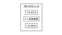
次いで、図1に示したメモリモジュール109の具体的な構成を、図3にブロック図として例示する。図3に示すメモリモジュール109は、カウンタ110と、記憶装置111と、DMAC112とを有する。カウンタ110は、コンフィギュレーションデータ105がロジックアレイ107に書き込まれた回数を、コンフィギュレーションデータ105の識別子ごとにカウントする機能を有する。記憶装置111は、コンフィギュレーションデータ105の識別子と、識別子ごとにカウントされたロジックアレイ107への書き込み回数とを含む管理情報を、記憶する機能を有する。上述したように、最後にロジックアレイ107に書き込まれた時間や、コンフィギュレーションデータのデータ量などが、管理情報として記憶装置111に記憶させることも可能である。なお、最後にロジックアレイ107に書き込まれた時間を管理情報として取得する場合、プロセッサ101において時間を計測し、その時間のデータをメモリモジュール109の記憶装置111に記憶させておけば良い。
Next, a specific configuration of the memory module 109 illustrated in FIG. 1 is illustrated as a block diagram in FIG. The memory module 109 illustrated in FIG. 3 includes a counter 110, a storage device 111, and a
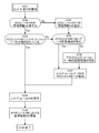
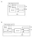
次いで、図2に示すフローチャートを用いて、PLD102にプロセッサ101からスレッドの実行が要求されてから、当該スレッドの実行が終了するまでの、PLD102の動作例について説明する。
Next, an exemplary operation of the
図2に示すフローチャートでは、まず、プロセッサ101からPLD102に、スレッドAの実行を要求する命令が送られる(A01:スレッドA実行の要求)。PLD102では、メモリモジュール109が、スレッドAに関連づけられたコンフィギュレーションデータAの識別子と、コンフィギュレーションデータAの使用状況のデータとを含む管理情報Aを有するか否かが、判断される(A02:メモリモジュール109が管理情報Aを有する)。
In the flowchart shown in FIG. 2, first, an instruction for requesting execution of the thread A is sent from the processor 101 to the PLD 102 (A01: request for executing thread A). In the
メモリモジュール109が管理情報Aを有する場合、過去にコンフィギュレーションデータAが少なくとも一回はメモリエレメント108に書き込まれたことがある、ということを意味する。この場合、PLD102では、メモリエレメント108に、コンフィギュレーションデータAが格納されているか否かが、判断される(A03:メモリエレメント108にコンフィギュレーションデータAが格納されている)。
When the memory module 109 has the management information A, it means that the configuration data A has been written to the memory element 108 at least once in the past. In this case, the
メモリエレメント108に、コンフィギュレーションデータAが格納されている場合、当該コンフィギュレーションデータAに従って、ロジックアレイ107において構成される論理回路の定義がなされる(A04:コンフィギュレーションAの実行)。 When the configuration data A is stored in the memory element 108, the logic circuit configured in the logic array 107 is defined according to the configuration data A (A04: execution of the configuration A).
一方、メモリモジュール109が管理情報Aを有さない場合、過去にコンフィギュレーションデータAがメモリエレメント108に書き込まれたことがない、ということを意味する。この場合、メモリモジュール109に格納されている管理情報に、管理情報Aを追加する(A05:メモリモジュール109への管理情報Aの追加)。そして、管理情報Aがメモリモジュール109に追加されたら、メモリエレメント108に、コンフィギュレーションデータAが格納できるだけの、空いている記憶領域があるか否かが、メモリモジュール109において判断される(A06:メモリエレメント108に空いている記憶領域がある)。 On the other hand, if the memory module 109 does not have the management information A, it means that the configuration data A has not been written to the memory element 108 in the past. In this case, management information A is added to the management information stored in the memory module 109 (A05: addition of management information A to the memory module 109). When the management information A is added to the memory module 109, the memory module 109 determines whether the memory element 108 has a free storage area that can store the configuration data A (A06: There is a free storage area in the memory element 108).
空いている記憶領域がある場合、コンフィギュレーションデータAをメモリエレメント108に格納する(A07:コンフィギュレーションデータAのメモリエレメント108への格納)。 If there is a free storage area, the configuration data A is stored in the memory element 108 (A07: storage of the configuration data A in the memory element 108).
空いている記憶領域がない場合、メモリモジュール109は、格納されている全ての管理情報を用いて、既にメモリエレメント108に格納されているコンフィギュレーションデータのうち、ロジックアレイ107に書き込まれた回数が少ない、すなわち上記回数の多さで並べたときの順位が下位であるコンフィギュレーションデータBを、選択する。そして、メモリエレメント108において、下位のコンフィギュレーションデータBが格納されている記憶領域を特定する(A08:下位のコンフィギュレーションデータBの記憶領域の特定)。 If there is no free storage area, the memory module 109 uses all the stored management information to determine the number of times the configuration data already stored in the memory element 108 has been written to the logic array 107. The configuration data B that is less in number, that is, in the lower order when arranged in the number of times described above, is selected. Then, in the memory element 108, the storage area in which the lower configuration data B is stored is specified (A08: specification of the storage area of the lower configuration data B).
なお、使用頻度が低いと見込まれるコンフィギュレーションデータBの選択に、いずれの管理情報を用いるか、そして管理情報をどのように用いるのかは、設計者が適宜選ぶことができる。例えば、ロジックアレイ107への書き込み回数が少ないコンフィギュレーションデータほど、そして、ロジックアレイ107に書き込まれた時間が古いコンフィギュレーションデータほど、使用頻度が低いと見込まれるため、次にロジックアレイ107に書き込まれるまでの期間が長いと予測される。よって、ロジックアレイ107への書き込み回数が最も少ないコンフィギュレーションデータを、コンフィギュレーションデータBとして選択することができる。或いは、最後にロジックアレイ107に書き込まれた時間が最も古いコンフィギュレーションデータを、コンフィギュレーションデータBとして選択することができる。或いは、ロジックアレイ107への書き込み回数が上位M番以降(Mは、2以上の自然数)であり、なおかつ最後にロジックアレイ107に書き込まれた時間が最も古いコンフィギュレーションデータを、コンフィギュレーションデータBとして選択することができる。 Note that the designer can appropriately select which management information is used for selecting the configuration data B expected to be used less frequently and how the management information is used. For example, the configuration data having a smaller number of times of writing to the logic array 107 and the configuration data having the older time of writing to the logic array 107 are expected to be used less frequently, and therefore are written to the logic array 107 next. The period until is expected to be long. Therefore, the configuration data with the smallest number of writes to the logic array 107 can be selected as the configuration data B. Alternatively, the configuration data with the oldest time last written in the logic array 107 can be selected as the configuration data B. Alternatively, the configuration data B is the configuration data whose number of times of writing to the logic array 107 is higher than the top M number (M is a natural number of 2 or more) and the last time of writing to the logic array 107 is the oldest. You can choose.
なお、データ量が小さいコンフィギュレーションデータであれば、再度メモリエレメント108に転送する必要が生じても、転送するデータ量を抑えることができる。よって、ロジックアレイ107への書き込み回数が上位M番以降であり、なおかつデータ量が最も小さいコンフィギュレーションデータを、コンフィギュレーションデータBとして選択することで、転送するデータ量を抑えることができる。 If the configuration data has a small data amount, the amount of data to be transferred can be suppressed even if it is necessary to transfer the configuration data to the memory element 108 again. Therefore, the amount of data to be transferred can be reduced by selecting, as the configuration data B, the configuration data having the smallest number of writes to the logic array 107 and the number of times higher than the top M.
下位のコンフィギュレーションデータBが格納されている記憶領域を特定(A08:下位のコンフィギュレーションデータBの記憶領域の特定)したら、コンフィギュレーションデータAをメモリエレメント108の上記記憶領域に格納する(A07:コンフィギュレーションデータAのメモリエレメント108への格納)。そして、当該コンフィギュレーションデータAに従って、ロジックアレイ107において構成される論理回路の定義がなされる(A04:コンフィギュレーションAの実行)。そして、定義された論理回路において、演算処理が行われることで、スレッドAが実行される。 After specifying the storage area in which the lower configuration data B is stored (A08: specifying the storage area of the lower configuration data B), the configuration data A is stored in the storage area of the memory element 108 (A07: Configuration data A is stored in the memory element 108). Then, in accordance with the configuration data A, a logic circuit configured in the logic array 107 is defined (A04: execution of configuration A). Then, thread A is executed by performing arithmetic processing in the defined logic circuit.
なお、ロジックアレイ107において構成される論理回路の定義がなされたら(A04:コンフィギュレーションAの実行)、メモリモジュール109において、管理情報Aを更新する(A09:メモリモジュール109における管理情報Aの更新)。例えば、管理情報Aに、ロジックアレイ107へ書き込み回数が含まれている場合は、回数を1回増やすように管理情報Aを更新する。或いは、管理情報Aに、最後にロジックアレイ107に書き込まれた時間が含まれている場合、上記時間が最新の時間になるように管理情報Aを更新する。 When a logic circuit configured in the logic array 107 is defined (A04: execution of configuration A), the management information A is updated in the memory module 109 (A09: update of the management information A in the memory module 109). . For example, if the management information A includes the number of writes to the logic array 107, the management information A is updated so that the number is increased by one. Alternatively, when the management information A includes the time last written in the logic array 107, the management information A is updated so that the time becomes the latest time.
管理情報Aを更新したら(A09:メモリモジュール109における管理情報Aの更新)、PLD102において行われる処理が終了する(A10:終了)。
When the management information A is updated (A09: update of the management information A in the memory module 109), the processing performed in the
なお、図2に示すフローチャートでは、管理情報Aの更新(A09:メモリモジュール109における管理情報Aの更新)を、ロジックアレイ107において構成される論理回路の定義(A04:コンフィギュレーションAの実行)が終了した後に行われているが、管理情報Aの更新は、スレッドAの実行を要求する命令をPLD102が受け取った後(A01:スレッドA実行の要求)であれば、いつでも可能である。
In the flowchart shown in FIG. 2, the management information A is updated (A09: update of the management information A in the memory module 109), and the logic circuit definition (A04: execution of configuration A) in the logic array 107 is performed. The management information A can be updated at any time after the
次いで、図1に示した記憶装置103に格納されている、アプリケーション104とコンフィギュレーションデータ105のデータ構造の模式図を、図4に示す。図4(A)に示す記憶装置103では、1つのアプリケーション104に対し、2つのコンフィギュレーションデータ105が関連づけられている場合を例示している。なお、1つのアプリケーション104に関連づけられているコンフィギュレーションデータ105の数は、3つ以上であっても良い。
Next, FIG. 4 shows a schematic diagram of the data structures of the application 104 and the
また、図4(B)に示す記憶装置103では、コンフィギュレーションデータ105が関連づけられていないアプリケーション104と、1つのコンフィギュレーションデータ105が関連づけられているアプリケーション104と、2つのコンフィギュレーションデータ105が関連づけられているアプリケーション104とが、混在している。
In addition, in the storage device 103 illustrated in FIG. 4B, the application 104 not associated with the
また、図4(C)に示す記憶装置103では、2つのアプリケーション104に対し、1つのコンフィギュレーションデータ105が共有するように関連づけられている場合を例示している。なお、1つのコンフィギュレーションデータ105を共有するように関連づけられているアプリケーション104の数は、3つ以上であっても良い。
Further, in the storage device 103 illustrated in FIG. 4C, a case where one
次いで、アプリケーション104を構成する複数のスレッドと、各スレッドを実行するプロセッサ101またはPLD102との関係を、図5(A)及び図5(B)に模式的に例示する。図5(A)及び図5(B)では、アプリケーション104が、スレッド120A、スレッド120B、スレッド120C、及びスレッド120Dを有している場合を例示している。そして、図5(A)及び図5(B)では、スレッド120A、スレッド120B、スレッド120C、スレッド120B、スレッド120Dの順番に、各スレッドを実行することで、アプリケーション104が実行される場合を、例示している。
Next, the relationship between a plurality of threads constituting the application 104 and the processor 101 or the
そして、図5(A)では、スレッド120A、スレッド120C、及びスレッド120Dを、プロセッサ101においてソフトウェア的に実行し、スレッド120Bを、PLD102においてハードウェア的に実行する場合を示している。図5(A)に示したアプリケーション104を実行する場合、スレッド120BをPLD102において実行するのに必要なコンフィギュレーションデータ105が、アプリケーション104に関連づけられて、図1に示した記憶装置103に格納されていればよい。
FIG. 5A shows a case where the
また、図5(B)では、スレッド120A及びスレッド120Bを、プロセッサ101においてソフトウェア的に実行し、スレッド120C及びスレッド120Dを、PLD102においてハードウェア的に実行する場合を示している。図5(B)に示したアプリケーション104を実行する場合、スレッド120CをPLD102において実行するのに必要なコンフィギュレーションデータ105と、スレッド120DをPLD102において実行するのに必要なコンフィギュレーションデータ105とが、アプリケーション104に関連づけられて、図1に示した記憶装置103に格納されていればよい。
FIG. 5B shows a case where the
次いで、メモリエレメント108が有するメモリセルの構成例について、図6を用いて説明する。図6(A)に、メモリセル120の回路図を一例として示す。メモリエレメント108には、メモリセル120が複数設けられており、各メモリセル120は、記憶素子121と、スイッチ122とを有する。
Next, a configuration example of a memory cell included in the memory element 108 is described with reference to FIGS. FIG. 6A illustrates a circuit diagram of the
記憶素子121には、容量素子、トランジスタなどの半導体素子を用いることができる。そして、記憶素子121は、容量素子、或いは、トランジスタのゲート電極と活性層の間に形成されるゲート容量に、電荷を蓄積させることで、データを記憶する。また、記憶素子121への電荷の供給と、当該記憶素子121からの電荷の放出と、当該記憶素子121における電荷の保持とは、スイッチ122により制御する。
As the
スイッチ122は、シリコンよりもバンドギャップが広く、真性キャリア密度がシリコンよりも低い半導体を、チャネル形成領域に含むトランジスタを用いる。このような半導体としては、例えば、シリコンの2倍以上の大きなバンドギャップを有する、酸化物半導体、炭化シリコン、窒化ガリウム、酸化ガリウムなどが挙げられる。上記半導体を有するトランジスタは、通常のシリコンやゲルマニウムなどの半導体で形成されたトランジスタに比べて、オフ電流を極めて小さくすることができる。よって、上記構成を有するトランジスタを、記憶素子121に流入した電荷を保持するためのスイッチ122として用いることで、記憶素子121からの電荷のリークを防ぐことができるので、データの保持期間を長く確保することができる。
As the
なお、メモリセル120は、必要に応じて、トランジスタ、ダイオード、抵抗素子、インダクタンスなどのその他の回路素子を、さらに有していても良い。
Note that the
なお、特に断りがない限り、本明細書でオフ電流とは、nチャネル型トランジスタにおいては、ドレイン端子をソース端子とゲート電極よりも高い電位とした状態において、ソース端子の電位を基準としたときのゲート電極の電位が0以下であるときに、ソース端子とドレイン端子の間に流れる電流のことを意味する。或いは、本明細書でオフ電流とは、pチャネル型トランジスタにおいては、ドレイン端子をソース端子とゲート電極よりも低い電位とした状態において、ソース端子の電位を基準としたときのゲート電極の電位が0以上であるときに、ソース端子とドレイン端子の間に流れる電流のことを意味する。 Note that unless otherwise specified, off-state current in this specification refers to an n-channel transistor in which the drain terminal is higher than the source terminal and the gate electrode, and the potential of the source terminal is used as a reference. It means a current that flows between the source terminal and the drain terminal when the potential of the gate electrode is 0 or less. Alternatively, in this specification, off-state current refers to that in a p-channel transistor, the potential of the gate electrode with respect to the potential of the source terminal in a state where the drain terminal is lower than the source terminal and the gate electrode. When it is 0 or more, it means a current flowing between the source terminal and the drain terminal.
なお、スイッチ122は、一のトランジスタで構成されていても良いし、複数のトランジスタで構成されていても良い。例えば、複数の直列に接続されたトランジスタを用いることで、よりオフ電流の小さなスイッチ122を形成することができ、よって、記憶素子121からの電荷のリークをより防ぐことができる。
Note that the
なお、本明細書において、トランジスタが直列に接続されている状態とは、第1のトランジスタのソース端子とドレイン端子のいずれか一方のみが、第2のトランジスタのソース端子とドレイン端子のいずれか一方のみに接続されている状態を意味する。また、トランジスタが並列に接続されている状態とは、第1のトランジスタのソース端子とドレイン端子のいずれか一方が、第2のトランジスタのソース端子とドレイン端子のいずれか一方に接続され、第1のトランジスタのソース端子とドレイン端子の他方が第2のトランジスタのソース端子とドレイン端子の他方に接続されている状態を意味する。 Note that in this specification, a state in which transistors are connected in series refers to only one of a source terminal and a drain terminal of a first transistor and one of a source terminal and a drain terminal of a second transistor. It means the state that is connected to only. In addition, the state in which the transistors are connected in parallel means that either the source terminal or the drain terminal of the first transistor is connected to either the source terminal or the drain terminal of the second transistor. This means that the other of the source terminal and the drain terminal of the transistor is connected to the other of the source terminal and the drain terminal of the second transistor.
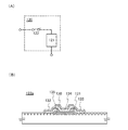
図6(B)に、スイッチ122に用いられるトランジスタ122aの断面構造を、一例として示す。ただし、図6(B)では、活性層として酸化物半導体を用いたトランジスタ122aを例示している。
FIG. 6B illustrates a cross-sectional structure of the
トランジスタ122aは、絶縁表面上に形成されたゲート電極130と、ゲート電極130上のゲート絶縁膜131と、ゲート絶縁膜131上の導電膜132、導電膜133と、ゲート絶縁膜131上においてゲート電極130と重なっており、なおかつ導電膜132、導電膜133上に形成された、活性層として機能する酸化物半導体膜134とを有する。さらに、トランジスタ122aは、導電膜132、導電膜133、及び酸化物半導体膜134上に形成された絶縁膜135を、その構成要素に含めても良い。
The
なお、電子供与体(ドナー)となる水分または水素などの不純物が低減され、なおかつ酸素欠損が低減されることにより高純度化された酸化物半導体(purified OS)は、i型(真性半導体)又はi型に限りなく近い。そのため、水分または水素などの不純物濃度が十分に低減され、なおかつ酸素欠損が低減されることにより高純度化された酸化物半導体膜を用いることにより、トランジスタのオフ電流を小さくすることができる。よって、高純度化された酸化物半導体膜を用いたトランジスタを、スイッチ122に用いることで、記憶素子121からの電荷のリークを防ぎ、データの保持期間を長く確保するという効果を高めることができる。
Note that an oxide semiconductor (purified OS) purified by reducing impurities such as moisture or hydrogen serving as an electron donor (donor) and reducing oxygen vacancies is an i-type (intrinsic semiconductor) or Close to i-type. Therefore, the off-state current of the transistor can be reduced by using an oxide semiconductor film which is highly purified by reducing the concentration of impurities such as moisture or hydrogen and reducing oxygen vacancies. Thus, by using a transistor including a highly purified oxide semiconductor film for the
具体的に、高純度化された酸化物半導体をチャネル形成領域に用いたトランジスタのオフ電流が小さいことは、いろいろな実験により証明できる。例えば、チャネル幅が1×106μmでチャネル長が10μmの素子であっても、ソース電極とドレイン電極間の電圧(ドレイン電圧)が1Vから10Vの範囲において、オフ電流が、半導体パラメータアナライザの測定限界以下、すなわち1×10⁻¹³A以下という特性を得ることができる。この場合、オフ電流をトランジスタのチャネル幅で規格化したオフ電流は、100zA/μm以下であることが分かる。また、容量素子とトランジスタとを接続して、容量素子に流入または容量素子から流出する電荷を当該トランジスタで制御する回路を用いて、オフ電流の測定を行った。当該測定では、高純度化された酸化物半導体膜を上記トランジスタのチャネル形成領域に用い、容量素子の単位時間あたりの電荷量の推移から当該トランジスタのオフ電流を測定した。その結果、トランジスタのソース電極とドレイン電極間の電圧が3Vの場合に、数十yA/μmという、さらに小さいオフ電流が得られることが分かった。従って、高純度化された酸化物半導体膜をチャネル形成領域に用いたトランジスタは、オフ電流が、結晶性を有するシリコンを用いたトランジスタに比べて著しく小さい。 Specifically, it can be proved by various experiments that the off-state current of a transistor in which a highly purified oxide semiconductor is used for a channel formation region is small. For example, even in an element having a channel width of 1 × 10 6 μm and a channel length of 10 μm, when the voltage between the source electrode and the drain electrode (drain voltage) is in the range of 1V to 10V, It is possible to obtain characteristics that are below the measurement limit, that is, 1 × 10 −13 A or less. In this case, it can be seen that the off-current obtained by normalizing the off-current with the channel width of the transistor is 100 zA / μm or less. In addition, off-state current was measured using a circuit in which a capacitor and a transistor were connected and charge flowing into or out of the capacitor was controlled by the transistor. In this measurement, a highly purified oxide semiconductor film was used for a channel formation region of the transistor, and the off-state current of the transistor was measured from the change in charge amount per unit time of the capacitor. As a result, it was found that when the voltage between the source electrode and the drain electrode of the transistor is 3 V, an even smaller off current of several tens of yA / μm can be obtained. Therefore, a transistor using a highly purified oxide semiconductor film for a channel formation region has significantly lower off-state current than a transistor using crystalline silicon.
また、酸化物半導体の中でもIn−Ga−Zn系酸化物、In−Sn−Zn系酸化物などは、炭化シリコン、窒化ガリウム、または酸化ガリウムとは異なり、スパッタリング法や湿式法により電気的特性の優れたトランジスタを作製することが可能であり、量産性に優れるといった利点がある。また、炭化シリコン、窒化ガリウム、または酸化ガリウムとは異なり、上記酸化物半導体であるIn−Ga−Zn系酸化物は室温でも成膜が可能なため、ガラス基板上への成膜、或いはシリコンを用いた集積回路上に電気的特性の優れたトランジスタを作製することが可能である。また、基板の大型化にも対応が可能である。 Further, among oxide semiconductors, an In—Ga—Zn-based oxide, an In—Sn—Zn-based oxide, or the like has electrical characteristics different from those of silicon carbide, gallium nitride, or gallium oxide by a sputtering method or a wet method. There is an advantage that an excellent transistor can be manufactured and the mass productivity is excellent. In addition, unlike silicon carbide, gallium nitride, or gallium oxide, an In—Ga—Zn-based oxide that is an oxide semiconductor can be formed even at room temperature. A transistor with excellent electrical characteristics can be manufactured over the used integrated circuit. Moreover, it is possible to cope with an increase in the size of the substrate.
なお、酸化物半導体としては、少なくともインジウム(In)あるいは亜鉛(Zn)を含むことが好ましい。また、該酸化物半導体を用いたトランジスタの電気的特性のばらつきを減らすためのスタビライザーとして、それらに加えてガリウム(Ga)を有することが好ましい。また、スタビライザーとしてスズ(Sn)を有することが好ましい。また、スタビライザーとしてハフニウム(Hf)を有することが好ましい。また、スタビライザーとしてアルミニウム(Al)を有することが好ましい。また、スタビライザーとしてジルコニウム(Zr)を含むことが好ましい。 Note that the oxide semiconductor preferably contains at least indium (In) or zinc (Zn). In addition, it is preferable that gallium (Ga) be included in addition to the stabilizer for reducing variation in electrical characteristics of the transistor including the oxide semiconductor. Moreover, it is preferable to have tin (Sn) as a stabilizer. Moreover, it is preferable to have hafnium (Hf) as a stabilizer. Moreover, it is preferable to have aluminum (Al) as a stabilizer. Moreover, it is preferable that zirconium (Zr) is included as a stabilizer.
また、他のスタビライザーとして、ランタノイドである、ランタン(La)、セリウム(Ce)、プラセオジム(Pr)、ネオジム(Nd)、サマリウム(Sm)、ユウロピウム(Eu)、ガドリニウム(Gd)、テルビウム(Tb)、ジスプロシウム(Dy)、ホルミウム(Ho)、エルビウム(Er)、ツリウム(Tm)、イッテルビウム(Yb)、ルテチウム(Lu)のいずれか一種または複数種を含んでいてもよい。 As other stabilizers, lanthanoids such as lanthanum (La), cerium (Ce), praseodymium (Pr), neodymium (Nd), samarium (Sm), europium (Eu), gadolinium (Gd), terbium (Tb) , Dysprosium (Dy), holmium (Ho), erbium (Er), thulium (Tm), ytterbium (Yb), or lutetium (Lu) may be included.
例えば、酸化物半導体として、酸化インジウム、酸化ガリウム、酸化スズ、酸化亜鉛、二元系金属の酸化物であるIn−Zn系酸化物、Sn−Zn系酸化物、Al−Zn系酸化物、Zn−Mg系酸化物、Sn−Mg系酸化物、In−Mg系酸化物、In−Ga系酸化物、三元系金属の酸化物であるIn−Ga−Zn系酸化物(IGZOとも表記する)、In−Al−Zn系酸化物、In−Sn−Zn系酸化物、Sn−Ga−Zn系酸化物、Al−Ga−Zn系酸化物、Sn−Al−Zn系酸化物、In−Hf−Zn系酸化物、In−La−Zn系酸化物、In−Pr−Zn系酸化物、In−Nd−Zn系酸化物、In−Sm−Zn系酸化物、In−Eu−Zn系酸化物、In−Gd−Zn系酸化物、In−Tb−Zn系酸化物、In−Dy−Zn系酸化物、In−Ho−Zn系酸化物、In−Er−Zn系酸化物、In−Tm−Zn系酸化物、In−Yb−Zn系酸化物、In−Lu−Zn系酸化物、四元系金属の酸化物であるIn−Sn−Ga−Zn系酸化物、In−Hf−Ga−Zn系酸化物、In−Al−Ga−Zn系酸化物、In−Sn−Al−Zn系酸化物、In−Sn−Hf−Zn系酸化物、In−Hf−Al−Zn系酸化物を用いることができる。 For example, as an oxide semiconductor, indium oxide, gallium oxide, tin oxide, zinc oxide, binary metal oxides such as In—Zn oxide, Sn—Zn oxide, Al—Zn oxide, Zn -Mg-based oxide, Sn-Mg-based oxide, In-Mg-based oxide, In-Ga-based oxide, In-Ga-Zn-based oxide which is an oxide of a ternary metal (also referred to as IGZO) In-Al-Zn-based oxide, In-Sn-Zn-based oxide, Sn-Ga-Zn-based oxide, Al-Ga-Zn-based oxide, Sn-Al-Zn-based oxide, In-Hf- Zn-based oxide, In-La-Zn-based oxide, In-Pr-Zn-based oxide, In-Nd-Zn-based oxide, In-Sm-Zn-based oxide, In-Eu-Zn-based oxide, In-Gd-Zn-based oxide, In-Tb-Zn-based oxide, In-Dy- n-based oxide, In-Ho-Zn-based oxide, In-Er-Zn-based oxide, In-Tm-Zn-based oxide, In-Yb-Zn-based oxide, In-Lu-Zn-based oxide, In-Sn-Ga-Zn-based oxides, In-Hf-Ga-Zn-based oxides, In-Al-Ga-Zn-based oxides, In-Sn-Al-Zn-based oxides that are quaternary metal oxides An oxide, an In—Sn—Hf—Zn-based oxide, or an In—Hf—Al—Zn-based oxide can be used.
なお、例えば、In−Ga−Zn系酸化物とは、InとGaとZnを含む酸化物という意味であり、InとGaとZnの比率は問わない。また、InとGaとZn以外の金属元素を含んでいてもよい。In−Ga−Zn系酸化物は、無電界時の抵抗が十分に高くオフ電流を十分に小さくすることが可能であり、また、移動度も高い。 Note that for example, an In—Ga—Zn-based oxide means an oxide containing In, Ga, and Zn, and there is no limitation on the ratio of In, Ga, and Zn. Moreover, metal elements other than In, Ga, and Zn may be included. In-Ga-Zn-based oxides have sufficiently high resistance when no electric field is applied, and can have a sufficiently low off-state current, and also have high mobility.
例えば、In:Ga:Zn=1:1:1(=1/3:1/3:1/3)あるいはIn:Ga:Zn=2:2:1(=2/5:2/5:1/5)の原子比のIn−Ga−Zn系酸化物やその組成の近傍の酸化物を用いることができる。あるいは、In:Sn:Zn=1:1:1(=1/3:1/3:1/3)、In:Sn:Zn=2:1:3(=1/3:1/6:1/2)あるいはIn:Sn:Zn=2:1:5(=1/4:1/8:5/8)の原子比のIn−Sn−Zn系酸化物やその組成の近傍の酸化物を用いるとよい。 For example, In: Ga: Zn = 1: 1: 1 (= 1/3: 1/3: 1/3) or In: Ga: Zn = 2: 2: 1 (= 2/5: 2/5: 1). / 5) atomic ratio In—Ga—Zn-based oxides and oxides in the vicinity of the composition can be used. Alternatively, In: Sn: Zn = 1: 1: 1 (= 1/3: 1/3: 1/3), In: Sn: Zn = 2: 1: 3 (= 1/3: 1/6: 1) / 2) or In: Sn: Zn = 2: 1: 5 (= 1/4: 1/8: 5/8) atomic ratio In—Sn—Zn-based oxide or an oxide in the vicinity of the composition. Use it.
例えば、In−Sn−Zn系酸化物では比較的容易に高い移動度が得られる。しかしながら、In−Ga−Zn系酸化物でも、バルク内欠陥密度を低減することにより移動度を上げることができる。 For example, high mobility can be obtained relatively easily with an In—Sn—Zn-based oxide. However, mobility can be increased by reducing the defect density in the bulk also in the case of using an In—Ga—Zn-based oxide.
以下では、酸化物半導体膜の構造について説明する。 Hereinafter, the structure of the oxide semiconductor film is described.
酸化物半導体膜は、単結晶酸化物半導体膜と非単結晶酸化物半導体膜とに大別される。非単結晶酸化物半導体膜とは、非晶質酸化物半導体膜、微結晶酸化物半導体膜、多結晶酸化物半導体膜、CAAC−OS(C Axis Aligned Crystalline Oxide Semiconductor)膜などをいう。 An oxide semiconductor film is classified roughly into a single crystal oxide semiconductor film and a non-single crystal oxide semiconductor film. The non-single-crystal oxide semiconductor film refers to an amorphous oxide semiconductor film, a microcrystalline oxide semiconductor film, a polycrystalline oxide semiconductor film, a CAAC-OS (C Axis Crystalline Oxide Semiconductor) film, or the like.
非晶質酸化物半導体膜は、膜中における原子配列が不規則であり、結晶成分を有さない酸化物半導体膜である。微小領域においても結晶部を有さず、膜全体が完全な非晶質構造の酸化物半導体膜が典型である。 An amorphous oxide semiconductor film is an oxide semiconductor film having an irregular atomic arrangement in the film and having no crystal component. An oxide semiconductor film which has no crystal part even in a minute region and has a completely amorphous structure as a whole is typical.
微結晶酸化物半導体膜は、例えば、1nm以上10nm未満の大きさの微結晶(ナノ結晶ともいう。)を含む。従って、微結晶酸化物半導体膜は、非晶質酸化物半導体膜よりも原子配列の規則性が高い。そのため、微結晶酸化物半導体膜は、非晶質酸化物半導体膜よりも欠陥準位密度が低いという特徴がある。 The microcrystalline oxide semiconductor film includes a microcrystal (also referred to as nanocrystal) with a size greater than or equal to 1 nm and less than 10 nm, for example. Therefore, the microcrystalline oxide semiconductor film has higher regularity of atomic arrangement than the amorphous oxide semiconductor film. Therefore, a microcrystalline oxide semiconductor film has a feature that the density of defect states is lower than that of an amorphous oxide semiconductor film.
CAAC−OS膜は、複数の結晶部を有する酸化物半導体膜の一つであり、ほとんどの結晶部は、一辺が100nm未満の立方体内に収まる大きさである。従って、CAAC−OS膜に含まれる結晶部は、一辺が10nm未満、5nm未満または3nm未満の立方体内に収まる大きさの場合も含まれる。CAAC−OS膜は、微結晶酸化物半導体膜よりも欠陥準位密度が低いという特徴がある。以下、CAAC−OS膜について詳細な説明を行う。 The CAAC-OS film is one of oxide semiconductor films having a plurality of crystal parts, and most of the crystal parts are large enough to fit in a cube whose one side is less than 100 nm. Therefore, the case where a crystal part included in the CAAC-OS film fits in a cube whose one side is less than 10 nm, less than 5 nm, or less than 3 nm is included. The CAAC-OS film is characterized by having a lower density of defect states than a microcrystalline oxide semiconductor film. Hereinafter, the CAAC-OS film is described in detail.
CAAC−OS膜を透過型電子顕微鏡(TEM:Transmission Electron Microscope)によって観察すると、結晶部同士の明確な境界、即ち結晶粒界(グレインバウンダリーともいう。)を確認することができない。そのため、CAAC−OS膜は、結晶粒界に起因する電子移動度の低下が起こりにくいといえる。 When the CAAC-OS film is observed with a transmission electron microscope (TEM), a clear boundary between crystal parts, that is, a grain boundary (also referred to as a grain boundary) cannot be confirmed. Therefore, it can be said that the CAAC-OS film is unlikely to decrease in electron mobility due to crystal grain boundaries.
CAAC−OS膜を、試料面と概略平行な方向からTEMによって観察(断面TEM観察)すると、結晶部において、金属原子が層状に配列していることを確認できる。金属原子の各層は、CAAC−OS膜の膜を形成する面(被形成面ともいう。)または上面の凹凸を反映した形状であり、CAAC−OS膜の被形成面または上面と平行に配列する。 When the CAAC-OS film is observed by TEM (cross-sectional TEM observation) from a direction substantially parallel to the sample surface, it can be confirmed that metal atoms are arranged in layers in the crystal part. Each layer of metal atoms has a shape reflecting unevenness of a surface (also referred to as a formation surface) or an upper surface on which the CAAC-OS film is formed, and is arranged in parallel with the formation surface or the upper surface of the CAAC-OS film. .
なお、本明細書において、「平行」とは、二つの直線が−10°以上10°以下の角度で配置されている状態をいう。従って、−5°以上5°以下の場合も含まれる。また、「垂直」とは、二つの直線が80°以上100°以下の角度で配置されている状態をいう。従って、85°以上95°以下の場合も含まれる。 In this specification, “parallel” refers to a state in which two straight lines are arranged at an angle of −10 ° to 10 °. Therefore, the case of −5 ° to 5 ° is also included. “Vertical” refers to a state in which two straight lines are arranged at an angle of 80 ° to 100 °. Therefore, the case of 85 ° to 95 ° is also included.
一方、CAAC−OS膜を、試料面と概略垂直な方向からTEMによって観察(平面TEM観察)すると、結晶部において、金属原子が三角形状または六角形状に配列していることを確認できる。しかしながら、異なる結晶部間で、金属原子の配列に規則性は見られない。 On the other hand, when the CAAC-OS film is observed by TEM (planar TEM observation) from a direction substantially perpendicular to the sample surface, it can be confirmed that metal atoms are arranged in a triangular shape or a hexagonal shape in the crystal part. However, there is no regularity in the arrangement of metal atoms between different crystal parts.
断面TEM観察および平面TEM観察より、CAAC−OS膜の結晶部は配向性を有していることがわかる。 From the cross-sectional TEM observation and the planar TEM observation, it is found that the crystal part of the CAAC-OS film has orientation.
CAAC−OS膜に対し、X線回折(XRD:X−Ray Diffraction)装置を用いて構造解析を行うと、例えばInGaZnO4の結晶を有するCAAC−OS膜のout−of−plane法による解析では、回折角(2θ)が31°近傍にピークが現れる場合がある。このピークは、InGaZnO4の結晶の(009)面に帰属されることから、CAAC−OS膜の結晶がc軸配向性を有し、c軸が被形成面または上面に概略垂直な方向を向いていることが確認できる。 When structural analysis is performed on a CAAC-OS film using an X-ray diffraction (XRD) apparatus, for example, in the analysis of a CAAC-OS film having an InGaZnO 4 crystal by an out-of-plane method, A peak may appear when the diffraction angle (2θ) is around 31 °. Since this peak is attributed to the (009) plane of the InGaZnO 4 crystal, the CAAC-OS film crystal has c-axis orientation, and the c-axis is in a direction substantially perpendicular to the formation surface or the top surface. Can be confirmed.
一方、CAAC−OS膜に対し、c軸に概略垂直な方向からX線を入射させるin−plane法による解析では、2θが56°近傍にピークが現れる場合がある。このピークは、InGaZnO4の結晶の(110)面に帰属される。InGaZnO4の単結晶酸化物半導体膜であれば、2θを56°近傍に固定し、試料面の法線ベクトルを軸(φ軸)として試料を回転させながら分析(φスキャン)を行うと、(110)面と等価な結晶面に帰属されるピークが6本観察される。これに対し、CAAC−OS膜の場合は、2θを56°近傍に固定してφスキャンした場合でも、明瞭なピークが現れない。 On the other hand, when the CAAC-OS film is analyzed by an in-plane method in which X-rays are incident from a direction substantially perpendicular to the c-axis, a peak may appear when 2θ is around 56 °. This peak is attributed to the (110) plane of the InGaZnO 4 crystal. In the case of a single crystal oxide semiconductor film of InGaZnO 4 , when 2θ is fixed in the vicinity of 56 ° and analysis (φ scan) is performed while rotating the sample with the normal vector of the sample surface as the axis (φ axis), Six peaks attributed to the crystal plane equivalent to the (110) plane are observed. On the other hand, in the case of a CAAC-OS film, a peak is not clearly observed even when φ scan is performed with 2θ fixed at around 56 °.
以上のことから、CAAC−OS膜では、異なる結晶部間ではa軸およびb軸の配向は不規則であるが、c軸配向性を有し、かつc軸が被形成面または上面の法線ベクトルに平行な方向を向いていることがわかる。従って、前述の断面TEM観察で確認された層状に配列した金属原子の各層は、結晶のab面に平行な面である。 From the above, in the CAAC-OS film, the orientation of the a-axis and the b-axis is irregular between different crystal parts, but the c-axis is aligned, and the c-axis is a normal line of the formation surface or the top surface. It can be seen that the direction is parallel to the vector. Therefore, each layer of metal atoms arranged in a layer shape confirmed by the above-mentioned cross-sectional TEM observation is a plane parallel to the ab plane of the crystal.
なお、結晶部は、CAAC−OS膜を成膜した際、または加熱処理などの結晶化処理を行った際に形成される。上述したように、結晶のc軸は、CAAC−OS膜の被形成面または上面の法線ベクトルに平行な方向に配向する。従って、例えば、CAAC−OS膜の形状をエッチングなどによって変化させた場合、結晶のc軸がCAAC−OS膜の被形成面または上面の法線ベクトルと平行にならないこともある。 Note that the crystal part is formed when a CAAC-OS film is formed or when crystallization treatment such as heat treatment is performed. As described above, the c-axis of the crystal is oriented in a direction parallel to the normal vector of the formation surface or the top surface of the CAAC-OS film. Therefore, for example, when the shape of the CAAC-OS film is changed by etching or the like, the c-axis of the crystal may not be parallel to the normal vector of the formation surface or the top surface of the CAAC-OS film.
また、CAAC−OS膜中の結晶化度が均一でなくてもよい。例えば、CAAC−OS膜の結晶部が、CAAC−OS膜の上面近傍からの結晶成長によって形成される場合、上面近傍の領域は、被形成面近傍の領域よりも結晶化度が高くなることがある。また、CAAC−OS膜に不純物を添加する場合、不純物が添加された領域の結晶化度が変化し、部分的に結晶化度の異なる領域が形成されることもある。 Further, the crystallinity in the CAAC-OS film is not necessarily uniform. For example, in the case where the crystal part of the CAAC-OS film is formed by crystal growth from the vicinity of the top surface of the CAAC-OS film, the region near the top surface can have a higher degree of crystallinity than the region near the formation surface. is there. In addition, in the case where an impurity is added to the CAAC-OS film, the crystallinity of a region to which the impurity is added changes, and a region having a different degree of crystallinity may be formed.
なお、InGaZnO4の結晶を有するCAAC−OS膜のout−of−plane法による解析では、2θが31°近傍のピークの他に、2θが36°近傍にもピークが現れる場合がある。2θが36°近傍のピークは、CAAC−OS膜中の一部に、c軸配向性を有さない結晶が含まれることを示している。CAAC−OS膜は、2θが31°近傍にピークを示し、2θが36°近傍にピークを示さないことが好ましい。 Note that when the CAAC-OS film including an InGaZnO 4 crystal is analyzed by an out-of-plane method, a peak may also appear when 2θ is around 36 ° in addition to the peak where 2θ is around 31 °. A peak at 2θ of around 36 ° indicates that a crystal having no c-axis alignment is included in part of the CAAC-OS film. The CAAC-OS film preferably has a peak at 2θ of around 31 ° and no peak at 2θ of around 36 °.
CAAC−OS膜を用いたトランジスタは、可視光や紫外光の照射による電気的特性の変動が小さい。よって、当該トランジスタは、信頼性が高い。 In a transistor using a CAAC-OS film, change in electrical characteristics due to irradiation with visible light or ultraviolet light is small. Therefore, the transistor has high reliability.
なお、酸化物半導体膜は、例えば、非晶質酸化物半導体膜、微結晶酸化物半導体膜、CAAC−OS膜のうち、二種以上を有する積層膜であってもよい。 Note that the oxide semiconductor film may be a stacked film including two or more of an amorphous oxide semiconductor film, a microcrystalline oxide semiconductor film, and a CAAC-OS film, for example.
CAAC−OS膜は、例えば、多結晶である金属酸化物ターゲットを用い、スパッタリング法によって成膜する。当該ターゲットにイオンが衝突すると、ターゲットに含まれる結晶領域がa−b面から劈開し、a−b面に平行な面を有する平板状またはペレット状のスパッタリング粒子として剥離することがある。この場合、当該平板状のスパッタリング粒子が、結晶状態を維持したまま基板に到達することで、CAAC−OS膜を成膜することができる。 The CAAC-OS film is formed by a sputtering method using a polycrystalline metal oxide target, for example. When ions collide with the target, a crystal region included in the target may be cleaved from the ab plane and separated as flat or pellet-like sputtered particles having a plane parallel to the ab plane. In this case, the flat-plate-like sputtered particle reaches the substrate while maintaining a crystalline state, whereby a CAAC-OS film can be formed.
また、CAAC−OS膜を成膜するために、以下の条件を適用することが好ましい。 In order to form the CAAC-OS film, the following conditions are preferably applied.
成膜時の不純物混入を低減することで、不純物によって結晶状態が崩れることを抑制できる。例えば、処理室内に存在する不純物濃度(水素、水、二酸化炭素および窒素など)を低減すればよい。また、成膜ガス中の不純物濃度を低減すればよい。具体的には、露点が−80℃以下、好ましくは−100℃以下である成膜ガスを用いる。 By reducing the mixing of impurities during film formation, the crystal state can be prevented from being broken by impurities. For example, the impurity concentration (hydrogen, water, carbon dioxide, nitrogen, etc.) existing in the treatment chamber may be reduced. Further, the impurity concentration in the deposition gas may be reduced. Specifically, a deposition gas having a dew point of −80 ° C. or lower, preferably −100 ° C. or lower is used.
また、成膜時の基板加熱温度を高めることで、基板到達後にスパッタリング粒子のマイグレーションが起こる。具体的には、基板加熱温度を100℃以上740℃以下、好ましくは200℃以上500℃以下として成膜する。成膜時の基板加熱温度を高めることで、平板状のスパッタリング粒子が基板に到達した場合、基板上でマイグレーションが起こり、スパッタリング粒子の平らな面が基板に付着する。 Further, by increasing the substrate heating temperature during film formation, migration of sputtered particles occurs after reaching the substrate. Specifically, the film is formed at a substrate heating temperature of 100 ° C. to 740 ° C., preferably 200 ° C. to 500 ° C. By increasing the substrate heating temperature at the time of film formation, when the flat sputtered particles reach the substrate, migration occurs on the substrate, and the flat surface of the sputtered particles adheres to the substrate.
また、成膜ガス中の酸素割合を高め、電力を最適化することで成膜時のプラズマダメージを軽減すると好ましい。成膜ガス中の酸素割合は、30体積%以上、好ましくは100体積%とする。 In addition, it is preferable to reduce plasma damage during film formation by increasing the oxygen ratio in the film formation gas and optimizing electric power. The oxygen ratio in the deposition gas is 30% by volume or more, preferably 100% by volume.
ターゲットの一例として、In−Ga−Zn系酸化物ターゲットについて以下に示す。 As an example of the target, an In—Ga—Zn-based oxide target is described below.
InOX粉末、GaOY粉末およびZnOZ粉末を所定のmol数比で混合し、加圧処理後、1000℃以上1500℃以下の温度で加熱処理をすることで多結晶であるIn−Ga−Zn系酸化物ターゲットとする。なお、X、YおよびZは任意の正数である。ここで、所定のmol数比は、例えば、InOX粉末、GaOY粉末およびZnOZ粉末が、2:2:1、8:4:3、3:1:1、1:1:1、4:2:3または3:1:2である。なお、粉末の種類、およびその混合するmol数比は、作製するターゲットによって適宜変更すればよい。 In-Ga-Zn which is polycrystalline by mixing InO X powder, GaO Y powder and ZnO Z powder at a predetermined mol number ratio, and after heat treatment at a temperature of 1000 ° C. to 1500 ° C. A system oxide target is used. X, Y and Z are arbitrary positive numbers. Here, the predetermined mole number ratio is, for example, 2: 2: 1, 8: 4: 3, 3: 1: 1, 1: 1: 1, 4 for InO X powder, GaO Y powder, and ZnO Z powder. : 2: 3 or 3: 1: 2. In addition, what is necessary is just to change suitably the kind of powder, and the mol number ratio to mix with the target to produce.
また、図6(B)では、トランジスタ122aが、一のゲート電極130に対応した一のチャネル形成領域を有する、シングルゲート構造である場合を例示している。しかし、トランジスタ122aは、電気的に接続された複数のゲート電極を有することで、一の活性層にチャネル形成領域を複数有する、マルチゲート構造であっても良い。
FIG. 6B illustrates the case where the
また、トランジスタ122aは、ゲート電極を活性層の片側において少なくとも有していれば良いが、活性層を間に挟んで存在する一対のゲート電極を有していても良い。トランジスタが、活性層を間に挟んで存在する一対のゲート電極を有している場合、一方のゲート電極にはスイッチングを制御するための信号が与えられ、他方のゲート電極は、電気的に絶縁されたフローティングの状態であっても良いし、電位が他から与えられている状態であっても良い。後者の場合、一対の電極に、同じ高さの電位が与えられていても良いし、他方のゲート電極にのみ接地電位などの固定の電位が与えられていても良い。他方のゲート電極に与える電位の高さを制御することで、トランジスタ122aの閾値電圧を制御することができる。
The
なお、本明細書において接続とは電気的な接続を意味しており、電流、電圧または電位が、供給可能、或いは伝送可能な状態に相当する。従って、接続している状態とは、直接接続している状態を必ずしも指すわけではなく、電流、電圧または電位が、供給可能、或いは伝送可能であるように、抵抗素子、ダイオード、トランジスタ、容量素子などの回路素子を介して間接的に接続している状態も、その範疇に含む。 Note that in this specification, connection means electrical connection and corresponds to a state where current, voltage, or a potential can be supplied or transmitted. Therefore, a connected state does not necessarily indicate a directly connected state, but a resistor, a diode, a transistor, or a capacitor so that current, voltage, or potential can be supplied or transmitted. The state of being indirectly connected through a circuit element such as is included in the category.
なお、図6(B)では、トランジスタ122aとしてMOSFETを例示しているが、スイッチ122に用いることができるトランジスタは、MESFET(Metal Semiconductor Field Effect Transistor)であっても良い。
6B illustrates a MOSFET as the
メモリエレメント108が上記構成のメモリセルを複数有することで、本発明の一態様に係る半導体装置100では、PLD102の有するメモリエレメント108において、SRAMのようにトランジスタのオフ電流により電力が消費されることがない。また、上記構成を有するメモリエレメント108は、DRAMよりもリフレッシュの頻度を低減することができるので、リフレッシュによる消費電力を大幅に削減することができる。また、データの書き込みに要する時間をEEPROMよりも短くすることができるので、PLD102のコンフィギュレーションに要する時間を短縮化し、アプリケーション104の高速処理を実現することができる。
When the memory element 108 includes a plurality of memory cells having the above structure, in the semiconductor device 100 according to one embodiment of the present invention, power is consumed in the memory element 108 included in the
次いで、メモリセルのより具体的な構成例について、図7を用いて説明する。なお、本明細書において、トランジスタのソース端子とは、活性層としての機能を有する半導体膜の一部であるソース領域、或いは活性層としての機能を有する半導体膜に接続されたソース電極を意味する。同様に、トランジスタのドレイン端子とは、活性層としての機能を有する半導体膜の一部であるドレイン領域、或いは活性層としての機能を有する半導体膜に接続されたドレイン電極を意味する。 Next, a more specific configuration example of the memory cell will be described with reference to FIGS. Note that in this specification, a source terminal of a transistor means a source region that is part of a semiconductor film that functions as an active layer or a source electrode that is connected to a semiconductor film that functions as an active layer. . Similarly, a drain terminal of a transistor means a drain region that is part of a semiconductor film that functions as an active layer or a drain electrode that is connected to a semiconductor film that functions as an active layer.
また、トランジスタが有するソース端子とドレイン端子は、トランジスタのチャネル型及びソース端子とドレイン端子に与えられる電位の高低によって、その呼び方が入れ替わる。一般的に、nチャネル型のトランジスタでは、ソース端子とドレイン端子のうち、低い電位が与えられる方がソース端子と呼ばれ、高い電位が与えられる方がドレイン端子と呼ばれる。また、pチャネル型のトランジスタでは、ソース端子とドレイン端子のうち、低い電位が与えられる方がドレイン端子と呼ばれ、高い電位が与えられる方がソース端子と呼ばれる。本明細書では、便宜上、ソース端子とドレイン端子とが固定されているものと仮定して、トランジスタの接続関係を説明する場合があるが、実際には上記電位の関係に従ってソース端子とドレイン端子の呼び方が入れ替わる。 The names of the source terminal and the drain terminal of the transistor interchange with each other depending on the channel type of the transistor and the level of potential applied to the source terminal and the drain terminal. In general, in an n-channel transistor, a source terminal and a drain terminal to which a lower potential is applied are called source terminals, and a higher potential is called a drain terminal. In a p-channel transistor, a source terminal and a drain terminal to which a low potential is applied is called a drain terminal, and a side to which a high potential is applied is called a source terminal. In this specification, for the sake of convenience, the connection relationship between transistors may be described on the assumption that the source terminal and the drain terminal are fixed. In practice, however, the source terminal and the drain terminal are connected in accordance with the above-described potential relationship. The name is changed.
図7(A)に示すメモリセル150は、スイッチ122として機能するトランジスタ151と、記憶素子121として機能する容量素子152とを有する。トランジスタ151のゲート電極は、ワード線WLに接続されている。また、トランジスタ151は、そのソース端子及びドレイン端子の一方がデータ線DLに接続されており、そのソース端子及びドレイン端子の他方が容量素子152の一方の電極に接続されている。容量素子152の他方の電極は、接地電位などの固定電位が与えられているノードに、接続されている。
A
図7(A)に示すメモリセル150では、データの書き込み時にトランジスタ151がオンになり、データ線DLからデータを含む信号の電位が、トランジスタ151を介して容量素子152の一方の電極に与えられる。そして、上記信号の電位に従って、容量素子152に蓄積されている電荷量が制御されることで、容量素子152へのデータの書き込みが行われる。
In the
次いで、データの保持時には、トランジスタ151がオフになり、容量素子152において電荷が保持される。上述したように、トランジスタ151はオフ電流が極めて小さいという特性を有している。そのため、容量素子152に蓄積された電荷はリークしづらく、トランジスタ151にシリコンなどの半導体材料を用いた場合に比べ、長い期間に渡ってデータの保持を行うことができる。
Next, when data is held, the
データの読み出し時には、トランジスタ151がオンになり、データ線DLを介して容量素子152に蓄積された電荷が取り出される。そして、上記電荷量の違いを読み取ることにより、データを読み出すことができる。
At the time of reading data, the
図7(B)に示すメモリセル153は、スイッチ122として機能するトランジスタ154と、記憶素子121として機能するトランジスタ155及び容量素子156とを有する。トランジスタ154のゲート電極は、第1ワード線WLaに接続されている。また、トランジスタ154は、そのソース端子及びドレイン端子の一方が第1データ線DLaに接続されており、そのソース端子及びドレイン端子の他方がトランジスタ155のゲート電極に接続されている。トランジスタ155は、そのソース端子及びドレイン端子の一方が、第2データ線DLbに接続されており、そのソース端子及びドレイン端子の他方が、所定の電位が与えられているノードに接続されている。容量素子156が有する一対の電極は、一方がトランジスタ155のゲート電極に接続され、他方が第2ワード線WLbに接続されている。
A
図7(B)に示すメモリセル153では、データの書き込み時にトランジスタ154がオンになり、第1データ線DLaからデータを含む信号の電位が、トランジスタ154を介してトランジスタ155のゲート電極に与えられる。そして、上記信号の電位に従って、トランジスタ155のゲート容量、及び容量素子156に蓄積される電荷量が制御されることで、トランジスタ155及び容量素子156へのデータの書き込みが行われる。
In the
次いで、データの保持時には、トランジスタ154がオフになり、トランジスタ155のゲート容量、及び容量素子156に蓄積された電荷が保持される。上述したように、トランジスタ154はオフ電流が極めて小さいという特性を有している。そのため、蓄積された上記電荷はリークしづらく、トランジスタ154にシリコンなどの半導体材料を用いた場合に比べ、長い期間に渡ってデータの保持を行うことができる。
Next, when data is held, the
データの読み出し時には、第2ワード線WLbの電位を変化させる。容量素子156が有する一対の電極の電位差は、電荷保存則により維持されたままなので、第2ワード線WLbの電位の変化は、トランジスタ155のゲート電極に与えられる。トランジスタ155は、そのゲート容量に蓄積されている電荷量によって閾値電圧が変化している。よって、トランジスタ155のゲート電極の電位が変化することで得られるトランジスタ155のドレイン電流の大きさから、蓄積されている電荷量の違いを読み取ることにより、データを読み出すことができる。
When reading data, the potential of the second word line WLb is changed. Since the potential difference between the pair of electrodes included in the
なお、記憶素子121として機能するトランジスタ155は、その活性層に、酸化物半導体膜が用いられていても良い。或いは、トランジスタ155の活性層に、酸化物半導体以外の、非晶質、微結晶、多結晶、または単結晶の、シリコン、またはゲルマニウムなどの半導体が用いられていても良い。メモリセル153内の全てのトランジスタの活性層に、酸化物半導体膜を用いることで、プロセスを簡略化することができる。また、記憶素子121として機能するトランジスタ155の活性層に、例えば、多結晶または単結晶のシリコンなどのように、酸化物半導体よりも高い移動度が得られる半導体材料を用いることで、メモリセル153からのデータの読み出しを高速で行うことができる。
Note that an oxide semiconductor film may be used for an active layer of the
図7(C)に示すメモリセル157は、一つのデータ線DLが、第1データ線DLaと第2データ線DLbの機能を併せ持っている点において、図7(B)に示すメモリセル153と異なっている。具体的に、図7(C)に示すメモリセル157は、スイッチ122として機能するトランジスタ158と、記憶素子121として機能するトランジスタ159及び容量素子160とを有する。トランジスタ158のゲート電極は、第1ワード線WLaに接続されている。また、トランジスタ158は、そのソース端子及びドレイン端子の一方がデータ線DLに接続されており、そのソース端子及びドレイン端子の他方がトランジスタ159のゲート電極に接続されている。トランジスタ159は、そのソース端子及びドレイン端子の一方がデータ線DLに接続されており、そのソース端子及びドレイン端子の他方が、所定の電位が与えられているノードに接続されている。容量素子160が有する一対の電極は、一方がトランジスタ159のゲート電極に接続され、他方が第2ワード線WLbに接続されている。
The
図7(C)に示すメモリセル157は、データの書き込み、保持、読み出しなどの動作は、図7(B)に示すメモリセル157と同様に行うことができる。
In the
次いで、図1に示すメモリエレメント108の構成例について、説明する。図8に、メモリエレメント108の構成を、ブロック図で一例として示す。 Next, a configuration example of the memory element 108 illustrated in FIG. 1 will be described. FIG. 8 shows a configuration of the memory element 108 as an example in a block diagram.
図8に示すメモリエレメント108は、メモリセル170を複数有するセルアレイ175と、駆動回路161とを有する。そして、駆動回路161は、入出力バッファ162と、メインアンプ163と、カラムデコーダ164と、ローデコーダ165と、スイッチ回路166と、プリチャージ回路167と、センスアンプ168と、書き込み回路169とを有する。 A memory element 108 illustrated in FIG. 8 includes a cell array 175 including a plurality of memory cells 170 and a driver circuit 161. The drive circuit 161 includes an input / output buffer 162, a main amplifier 163, a column decoder 164, a row decoder 165, a switch circuit 166, a precharge circuit 167, a sense amplifier 168, and a write circuit 169. .
入出力バッファ162は、駆動回路161またはセルアレイ175の駆動に用いる各種信号、及び、セルアレイ175に書き込まれるコンフィギュレーションデータの、メモリエレメント108への入力を制御する機能を有する。また、入出力バッファ162は、セルアレイ175からコンフィギュレーションデータを読み出す場合、当該読み出されたコンフィギュレーションデータの、メモリエレメント108からの出力を制御する機能を有する。 The input / output buffer 162 has a function of controlling input of various signals used for driving the driver circuit 161 or the cell array 175 and configuration data written to the cell array 175 to the memory element 108. The input / output buffer 162 has a function of controlling the output of the read configuration data from the memory element 108 when the configuration data is read from the cell array 175.
ローデコーダ165は、例えばメモリセル170が、図7(A)に示したメモリセル150と同じ構成を有している場合、ワード線WLに与える電位を制御することで、セルアレイ175においてメモリセル170を、指定されたアドレスに従って行ごとに選択する機能を有する。カラムデコーダ164は、スイッチ回路166の動作を制御することで、コンフィギュレーションデータの書き込み時、または読み出し時の、列方向におけるメモリセル170の選択を、指定されたアドレスに従って行う機能を有する。
For example, when the memory cell 170 has the same structure as the
スイッチ回路166は、例えばメモリセル170が、図7(A)に示したメモリセル150と同じ構成を有している場合、データ線DLとメインアンプ163の間の接続と、データ線DLと書き込み回路169の間の接続とを行う機能を有する。書き込み回路169は、指定されたアドレスのメモリセル170に、スイッチ回路166を介してコンフィギュレーションデータを書き込む機能を有する。
For example, in the case where the memory cell 170 has the same structure as the
センスアンプ168は、メモリセル170からコンフィギュレーションデータを読み出すときに、データ線DLの電位の変化を増幅させる機能を有する。また、センスアンプ168は、メモリセル170に書き込まれたコンフィギュレーションデータ、或いはメモリセル170から読み出されたコンフィギュレーションデータを、一時的に記憶する機能を有する。 The sense amplifier 168 has a function of amplifying a change in potential of the data line DL when reading configuration data from the memory cell 170. In addition, the sense amplifier 168 has a function of temporarily storing configuration data written in the memory cell 170 or configuration data read from the memory cell 170.
メインアンプ163は、センスアンプ168により増幅されたデータ線DLの電位を用いて、コンフィギュレーションデータを読み出す機能を有する。プリチャージ回路167は、コンフィギュレーションデータの読み出し前に、データ線DLの電位をリセットする機能を有する。 The main amplifier 163 has a function of reading configuration data using the potential of the data line DL amplified by the sense amplifier 168. The precharge circuit 167 has a function of resetting the potential of the data line DL before reading configuration data.
なお、メモリエレメント108は、指定されたメモリセル170のアドレスを、一時的に記憶することができるアドレスバッファを、有していても良い。 Note that the memory element 108 may have an address buffer that can temporarily store the address of the designated memory cell 170.
次いで、図9に、一列のメモリセル170に対応した、センスアンプ168、プリチャージ回路167、スイッチ回路166、及びメインアンプ163の接続構造を例示する。なお、図9では、メモリセル170が、図7(A)に示したメモリセル150と同じ構成を有している場合を、例示している。
Next, FIG. 9 illustrates a connection structure of the sense amplifier 168, the precharge circuit 167, the switch circuit 166, and the main amplifier 163 corresponding to the memory cells 170 in one row. Note that FIG. 9 illustrates the case where the memory cell 170 has the same structure as the
メモリセル170はトランジスタ151と容量素子152とを有している。そして、メモリセル170は、データ線DLaに接続されている。また、センスアンプ168、プリチャージ回路167、及びスイッチ回路166は、データ線DLa及びデータ線DLbに接続されている。データ線DLa及びデータ線DLbは、複数のメモリセル170にそれぞれ接続された複数のデータ線DLの一つに、それぞれ相当するものとする。ただし、データ線DLa及びデータ線DLbに接続された全てのメモリセル170は、互いに異なるワード線WLに接続されているものとする。
The memory cell 170 includes a
具体的に、図9では、センスアンプ168がラッチ型である場合を例示している。センスアンプ168は、pチャネル型のトランジスタ515及びトランジスタ516と、nチャネル型のトランジスタ517及びトランジスタ518とを有している。トランジスタ515は、ソース端子及びドレイン端子の一方が端子SPに接続され、他方がトランジスタ516及びトランジスタ518のゲート電極と、データ線DLaとに接続されている。トランジスタ517は、ソース端子及びドレイン端子の一方がトランジスタ516及びトランジスタ518のゲート電極と、データ線DLaとに接続され、他方が端子SNに接続されている。トランジスタ516は、ソース端子及びドレイン端子の一方が端子SPに接続され、他方がトランジスタ515及びトランジスタ517のゲート電極と、データ線DLbとに接続されている。トランジスタ518は、ソース端子及びレイン端子の一方がトランジスタ515及びトランジスタ517のゲート電極と、データ線DLbとに接続され、他方が端子SNに接続されている。
Specifically, FIG. 9 illustrates the case where the sense amplifier 168 is a latch type. The sense amplifier 168 includes p-
また、プリチャージ回路167は、nチャネル型のトランジスタ519乃至トランジスタ521を有している。トランジスタ519乃至トランジスタ521は、pチャネル型であっても良い。トランジスタ519のソース端子及びドレイン端子は、一方がデータ線DLaに接続され、他方が端子Preに接続されている。トランジスタ520のソース端子及びドレイン端子は、一方がデータ線DLbに接続され、他方が端子Preに接続されている。トランジスタ521のソース端子及びドレイン端子は、一方がデータ線DLaに接続され、他方がデータ線DLbに接続されている。そして、トランジスタ519乃至トランジスタ521は、それぞれのゲート電極が配線PLに接続されている。
The precharge circuit 167 includes n-
スイッチ回路166は、nチャネル型のトランジスタ522及びトランジスタ523を有している。トランジスタ522及びトランジスタ523は、pチャネル型トランジスタであっても良い。トランジスタ522のソース端子及びドレイン端子は、一方がデータ線DLaに接続され、他方が配線IOaに接続されている。トランジスタ523のソース端子及びドレイン端子は、一方がデータ線DLbに接続され、他方が配線IObに接続されている。そして、トランジスタ522及びトランジスタ523は、それぞれのゲート電極が端子CSLに接続されている。端子CSLの電位は、カラムデコーダ164によって制御される。
The switch circuit 166 includes an n-
配線IOa及び配線IObは、メインアンプ163に接続されている。また、書き込み回路169は、コンフィギュレーションデータに従って、配線IOa及び配線IObへの電位の供給を行う機能を有する。 The wiring IOa and the wiring IOb are connected to the main amplifier 163. Further, the writing circuit 169 has a function of supplying a potential to the wiring IOa and the wiring IOb in accordance with the configuration data.
なお、センスアンプ168は上述したようなラッチ型に限定されず、カレントミラー型やシングルエンド型であっても良い。シングルエンド型のセンスアンプ168を用いる場合、データ線DLbの電位をリセットする必要がないので、プリチャージ回路167においてトランジスタ520及びトランジスタ521を省略することができる。
The sense amplifier 168 is not limited to the latch type as described above, and may be a current mirror type or a single end type. In the case where the single-ended sense amplifier 168 is used, the
また、データ線DLa及びデータ線DLbの組み合わせは、アレイ方式によって適宜決めることができる。本発明の一態様では、折り返し方式、クロスポイント方式、開放方式などのアレイ方式を用いることができ、これらのアレイ方式に合わせて、複数のメモリセル170にそれぞれ接続された複数のデータ線DLのうち、いずれか2つのデータ線DLと、メインアンプ163とを、スイッチ回路166により接続すれば良い。ただし、上述したように、データ線DLa及びデータ線DLbに接続された全てのメモリセル170は、互いに異なるワード線WLに接続されているものとする。 Further, the combination of the data line DLa and the data line DLb can be determined as appropriate depending on the array method. In one embodiment of the present invention, an array method such as a folding method, a cross point method, or an open method can be used. In accordance with these array methods, a plurality of data lines DL connected to a plurality of memory cells 170 can be used. Of these, any two data lines DL and the main amplifier 163 may be connected by the switch circuit 166. However, as described above, it is assumed that all the memory cells 170 connected to the data line DLa and the data line DLb are connected to different word lines WL.
書き込み回路169からコンフィギュレーションデータをメモリセル170に書き込む場合、まず、端子SPにハイレベルの電位VH_SPを与え、端子SNにローレベルの電位VL_SPを与えることで、センスアンプ168をオンの状態とする。そして、書き込み回路169によって、配線IOa及び配線IObの電位を、コンフィギュレーションデータに従った高さに制御し、スイッチ回路166においてトランジスタ522及びトランジスタ523をオンにする。上記構成により、データ線DLaに配線IOaの電位が与えられ、データ線DLbに配線IObの電位が与えられる。次いで、ワード線WLを選択し、トランジスタ151をオンにすることで、データ線DLaと容量素子152を接続する。そして、データ線DLaの電位に従い容量素子152に電荷が蓄積されることで、メモリセル170にコンフィギュレーションデータが書き込まれる。
When writing configuration data from the writing circuit 169 to the memory cell 170, first, the sense amplifier 168 is turned on by applying the high-level potential VH_SP to the terminal SP and the low-level potential VL_SP to the terminal SN. . Then, the potential of the wiring IOa and the wiring IOb is controlled to a height according to the configuration data by the writing circuit 169, and the
なお、データ線DLaに配線IOaの電位が与えられ、データ線DLbに配線IObの電位が与えられた後は、スイッチ回路166においてトランジスタ522及びトランジスタ523をオフにしても、センスアンプ168がオンの状態にあるならば、データ線DLaの電位とデータ線DLbの電位の高低の関係は、センスアンプ168により保持される。よって、スイッチ回路166においてトランジスタ522及びトランジスタ523をオンからオフに変更するタイミングは、ワード線WLを選択する前であっても、後であっても、どちらでも良い。
Note that after the potential of the wiring IOa is applied to the data line DLa and the potential of the wiring IOb is applied to the data line DLb, even if the
次いで、図1に示したプロセッサ101の、具体的な構成例について説明する。図10に、プロセッサ101の構成をブロック図で一例として示す。 Next, a specific configuration example of the processor 101 illustrated in FIG. 1 will be described. FIG. 10 is a block diagram illustrating an example of the configuration of the processor 101.
図10に示すプロセッサ101は、制御装置601と、演算装置602と、メインメモリ603と、入力装置604と、出力装置605、IF(インターフェース)606と、緩衝記憶装置607とを有する。
The processor 101 illustrated in FIG. 10 includes a
制御装置601は、プロセッサ101が有する演算装置602、メインメモリ603、入力装置604、出力装置605、IF606、緩衝記憶装置607の動作を統括的に制御することで、入力されたアプリケーションなどのプログラムに含まれる命令をデコードし、実行する機能を有する。演算装置602は、四則演算、論理演算などの各種演算処理を行う機能を有する。
The
なお、図10では、制御装置601と演算装置602とを独立したブロックとしてそれぞれ図示しているが、プロセッサ101は、制御装置601の機能と、演算装置602の機能とを併せ持った中央演算処理装置を、制御装置601及び演算装置602の代わりに有していても良い。
In FIG. 10, the
メインメモリ603には、制御装置601において実行される、複数の命令で構成されるアプリケーションなどのプログラムと、演算装置602における演算処理に用いられるデータとを、記憶する機能を有する。
The
緩衝記憶装置607は、演算装置602の演算処理の途中で得られたデータ、或いは演算装置602の演算処理の結果得られたデータなどを記憶する機能を有する。また、アプリケーションなどのプログラムを一時的に記憶する機能を有していても良い。
The
入力装置604は、半導体装置の外部から入力される命令を、プロセッサ101に送る機能を有する。入力装置604として、例えば、キーボード、マウス、タッチパネルなどを用いることができる。
The
出力装置605は、プロセッサ101の動作状態、アプリケーションなどのプログラムの実行により得られた結果などを、情報として出力する機能を有する。出力装置605として、例えば、ディスプレイ、プロジェクタ、プリンター、プロッター、音声出力装置などを用いることができる。
The
IF606は、図1に示した記憶装置103及びPLD102とプロセッサ101との間におけるデータの経路に相当する。記憶装置103に格納されているアプリケーション104及びコンフィギュレーションデータ105は、IF606を介してプロセッサ101に入力される。また、PLD102におけるスレッドの実行により得られたデータは、PLD102からIF606を介してプロセッサ101に入力される。また、プロセッサ101から出力される各種の命令やデータは、IF606を介して記憶装置103またはPLD102に送られる。
The
なお、プロセッサ101は、PLD102が有するDMACとは別に、DMACを有していても良い。
Note that the processor 101 may include a DMAC in addition to the DMAC included in the
制御装置601において命令の実行が繰り返されることで、プログラムが実行される。
The program is executed by repeatedly executing the instruction in the
次いで、図1に示したLE106の、具体的な構成例について説明する。
Next, a specific configuration example of the
図11(A)に、LE106の一形態を例示する。図11(A)に示すLE106は、LUT(ルックアップテーブル)180と、レジスタ181とを有する。LUT180は、コンフィギュレーションデータ105の内容によって、実行される論理演算が異なる。そして、コンフィギュレーションデータ105が確定すると、LUT180は、複数の入力値に対する一の出力値が定まる。そして、LUT180からは、上記出力値を含む出力信号が出力される。レジスタ181は、LUT180からの出力信号を保持し、クロック信号CLKに同期して当該出力信号に対応した信号を出力する。
FIG. 11A illustrates an example of the
なお、LE106がさらにマルチプレクサ回路を有し、当該マルチプレクサ回路によって、LUT180からの出力信号がレジスタ181を経由するか否かを選択できるようにしても良い。
Note that the
また、コンフィギュレーションデータ105によって、レジスタ181の種類を定義できる構成にしても良い。具体的には、コンフィギュレーションデータ105によって、レジスタ181がD型レジスタ、T型レジスタ、JK型レジスタ、またはRS型レジスタのいずれかの機能を有するようにしても良い。
Further, the
また、LE106が、図1に示したメモリエレメント108から送られてきたコンフィギュレーションデータ105を、LE106内において記憶するための記憶装置(コンフィギュレーションメモリ)を、有していても良い。図11(B)に示すLE106は、図11(A)に示したLE106に、コンフィギュレーションメモリ182をさらに追加した構成を有する。コンフィギュレーションメモリ182を設けることで、同一のコンフィギュレーションデータ105に従って、LE106にて実行される論理演算を再度定める動作を、メモリエレメント108から直接送られてきたコンフィギュレーションデータ105を用いる場合よりも、より高速で行うことができる。
Further, the
次いで、LE106が有するLUT180の構成例について説明する。LUT180は複数のマルチプレクサを用いて構成することができる。そして、複数のマルチプレクサの入力端子及び制御端子のうちのいずれかに、コンフィギュレーションデータ105が入力される構成とすることができる。
Next, a configuration example of the
図12(A)に、LE106が有するLUT180の一態様を示す。図12(A)において、LUT180は、2入力のマルチプレクサを7つ(マルチプレクサ31、マルチプレクサ32、マルチプレクサ33、マルチプレクサ34、マルチプレクサ35、マルチプレクサ36、マルチプレクサ37)用いて構成されている。マルチプレクサ31乃至マルチプレクサ34の各入力端子が、LUT180の入力端子M1乃至M8に相当する。
FIG. 12A illustrates one mode of the
マルチプレクサ31乃至マルチプレクサ34の各制御端子は電気的に接続されており、上記制御端子が、LUT180の入力端子IN3に相当する。マルチプレクサ31の出力端子、及びマルチプレクサ32の出力端子は、マルチプレクサ35の2つの入力端子と電気的に接続され、マルチプレクサ33の出力端子、及びマルチプレクサ34の出力端子は、マルチプレクサ36の2つの入力端子と電気的に接続されている。マルチプレクサ35及びマルチプレクサ36の各制御端子は電気的に接続されており、上記制御端子が、LUT180の入力端子IN2に相当する。マルチプレクサ35の出力端子、及びマルチプレクサ36の出力端子は、マルチプレクサ37の2つの入力端子と電気的に接続されている。マルチプレクサ37の制御端子は、LUT180の入力端子IN1に相当する。マルチプレクサ37の出力端子がLUT180の出力端子OUTに相当する。
The control terminals of the
入力端子M1乃至入力端子M8、及び入力端子IN1乃至入力端子IN3のいずれかに、メモリセル170からコンフィギュレーションデータ105の電位を入力することによって、LUT180によって行われる論理演算の種類を定めることができる。
By inputting the potential of the
例えば、図12(A)のLUT180において、入力端子M1乃至入力端子M8に、デジタル値が”0”、”1”、”0”、”1”、”0”、”1”、”1”、”1”であるコンフィギュレーションデータ105をそれぞれ入力した場合、図12(C)に示す等価回路の機能を実現することができる。
For example, in the
図12(B)において、LUT180は、2入力のマルチプレクサを3つ(マルチプレクサ41、マルチプレクサ42、マルチプレクサ43)と、2入力のOR回路44とを用いて構成されている。
In FIG. 12B, the
マルチプレクサ41の出力端子、及びマルチプレクサ42の出力端子は、マルチプレクサ43の2つの入力端子と電気的に接続されている。OR回路44の出力端子はマルチプレクサ43の制御端子に電気的に接続されている。マルチプレクサ43の出力端子がLUT180の出力端子OUTに相当する。
The output terminal of the
そして、マルチプレクサ41の制御端子A1、入力端子A2及び入力端子A3、マルチプレクサ42の制御端子A6、入力端子A4及び入力端子A5、OR回路44の入力端子A7及び入力端子A8のいずれかに、コンフィギュレーションメモリから、当該コンフィギュレーションメモリに格納されたコンフィギュレーションデータに対応した出力信号を入力することによって、LUT180によって行われる論理演算の種類を定めることができる。
The control terminal A1, the input terminal A2 and the input terminal A3 of the
例えば、図12(B)のLUT180において、入力端子A2、入力端子A4、入力端子A5、制御端子A6、入力端子A8に、コンフィギュレーションメモリから、デジタル値が”0”、”1”、”0”、”0”、”0”である当該コンフィギュレーションメモリに格納されたコンフィギュレーションデータに対応した出力信号をそれぞれ入力した場合、図12(C)に示す等価回路の機能を実現することができる。なお、上記構成の場合、制御端子A1、入力端子A3、入力端子A7がそれぞれ入力端子IN1、入力端子IN2、入力端子IN3に相当する。
For example, in the
なお、図12(A)及び図12(B)では、2入力のマルチプレクサを用いて構成したLUT180の例を示したが、より多くの入力のマルチプレクサを用いて構成したLUT180であっても良い。
12A and 12B illustrate an example of the
また、LUT180は、マルチプレクサの他に、ダイオード、抵抗素子、論理回路(或いは論理素子)、スイッチのいずれかまたは全てを更に有していても良い。論理回路(或いは論理素子)としては、バッファ、インバータ、NAND回路、NOR回路、スリーステートバッファ、クロックドインバータ等を用いることができる。スイッチとしては、例えばアナログスイッチ、トランジスタ等を用いることができる。
The
また、図12(A)や図12(B)に示したLUT180を用いて、図12(C)の様な3入力1出力の論理演算を行う場合について示したがこれに限定されない。入力するコンフィギュレーションデータ105を適宜定めることによって、より多くの入力、多くの出力の論理演算を実現することができる。
Further, although the case where a logical operation of three inputs and one output as shown in FIG. 12C is performed using the
なお、コンフィギュレーションデータ105によって定められるのは、LE106で実行される論理演算だけではない。LE106どうしの接続構造も、コンフィギュレーションデータ105によって定められる。具体的に、LE106どうしの接続は、ロジックアレイ107に設けられた配線エレメントによって行われる。配線エレメントは、複数の配線で構成される配線群と、配線群を構成する配線どうしの接続を制御するスイッチとを有する。
Note that what is defined by the
図13(A)にロジックアレイ107の構造の一部を、一例として模式的に示す。図13(A)に示すロジックアレイ107は、複数のLE106と、複数のLE106のいずれかに接続された配線群321と、配線群321を構成する配線どうしの接続を制御するスイッチ322とを有する。配線群321及びスイッチ322が、配線エレメント323に相当する。スイッチ322によって制御される配線どうしの接続構造は、コンフィギュレーションデータ105によって定められる。
FIG. 13A schematically illustrates part of the structure of the logic array 107 as an example. A logic array 107 illustrated in FIG. 13A includes a plurality of
図13(B)に、スイッチ322の構成例を示す。図13(B)に示すスイッチ322は、配線群321に含まれる配線325と配線326の接続構造を制御する機能を有する。具体的に、スイッチ322は、トランジスタ327乃至トランジスタ332を有する。トランジスタ327は、配線325におけるPointAと、配線326におけるPointCの電気的な接続を制御する機能を有する。トランジスタ328は、配線325におけるPointBと、配線326におけるPointCの電気的な接続を制御する機能を有する。トランジスタ329は、配線325におけるPointAと、配線326におけるPointDの電気的な接続を制御する機能を有する。トランジスタ330は、配線325におけるPointBと、配線326におけるPointDの電気的な接続を制御する機能を有する。トランジスタ331は、配線325におけるPointAとPointBの電気的な接続を制御する機能を有する。トランジスタ332は、配線326におけるPointCとPointDの電気的な接続を制御する機能を有する。
FIG. 13B illustrates a configuration example of the
そして、トランジスタ327乃至トランジスタ332のオンまたはオフの選択(スイッチング)は、トランジスタ327乃至トランジスタ332のゲート電極310に与えられる、コンフィギュレーションデータ105の電位により行われる。
Then, on / off selection (switching) of the
また、スイッチ322は、配線群321と、ロジックアレイ107の出力端子324の、電気的な接続を制御する機能を有する。
The
(実施の形態2)
本発明の一態様に係る半導体装置は、表示機器、パーソナルコンピュータ、記録媒体を備えた画像再生装置(代表的にはDVD:Digital Versatile Disc等の記録媒体を再生し、その画像を表示しうるディスプレイを有する装置)に用いることができる。その他に、本発明の一態様に係る半導体装置を用いることができる電子機器として、携帯電話、携帯型を含むゲーム機、携帯情報端末、電子書籍、ビデオカメラ、デジタルスチルカメラ、ゴーグル型ディスプレイ(ヘッドマウントディスプレイ)、ナビゲーションシステム、音響再生装置(カーオーディオ、デジタルオーディオプレイヤー等)、複写機、ファクシミリ、プリンター、プリンター複合機、現金自動預け入れ払い機(ATM)、自動販売機などが挙げられる。これら電子機器の具体例を図14に示す。
(Embodiment 2)
A semiconductor device according to one embodiment of the present invention includes a display device, a personal computer, and an image reproducing device including a recording medium (typically a display that can reproduce a recording medium such as a DVD: Digital Versatile Disc and display the image) Device). In addition, as an electronic device in which the semiconductor device according to one embodiment of the present invention can be used, a mobile phone, a game machine including a portable type, a portable information terminal, an electronic book, a video camera, a digital still camera, a goggle type display (head Mount display), navigation system, sound reproduction device (car audio, digital audio player, etc.), copying machine, facsimile, printer, printer multifunction device, automatic teller machine (ATM), vending machine, and the like. Specific examples of these electronic devices are shown in FIGS.
図14(A)は携帯型ゲーム機であり、筐体5001、筐体5002、表示部5003、表示部5004、マイクロホン5005、スピーカー5006、操作キー5007、スタイラス5008等を有する。なお、図14(A)に示した携帯型ゲーム機は、2つの表示部5003と表示部5004とを有しているが、携帯型ゲーム機が有する表示部の数は、これに限定されない。
FIG. 14A illustrates a portable game machine, which includes a
図14(B)は携帯情報端末であり、第1筐体5601、第2筐体5602、第1表示部5603、第2表示部5604、接続部5605、操作キー5606等を有する。第1表示部5603は第1筐体5601に設けられており、第2表示部5604は第2筐体5602に設けられている。そして、第1筐体5601と第2筐体5602とは、接続部5605により接続されており、第1筐体5601と第2筐体5602の間の角度は、接続部5605により変更が可能となっている。第1表示部5603における映像の切り替えを、接続部5605における第1筐体5601と第2筐体5602との間の角度に従って、行う構成としても良い。また、第1表示部5603及び第2表示部5604の少なくとも一方に、位置入力装置としての機能が付加された表示装置を用いるようにしても良い。なお、位置入力装置としての機能は、表示装置にタッチパネルを設けることで付加することができる。或いは、位置入力装置としての機能は、フォトセンサとも呼ばれる光電変換素子を表示装置の画素部に設けることでも、付加することができる。
FIG. 14B illustrates a portable information terminal which includes a
図14(C)はノート型パーソナルコンピュータであり、筐体5401、表示部5402、キーボード5403、ポインティングデバイス5404等を有する。
FIG. 14C illustrates a laptop personal computer, which includes a
図14(D)はビデオカメラであり、第1筐体5801、第2筐体5802、表示部5803、操作キー5804、レンズ5805、接続部5806等を有する。操作キー5804及びレンズ5805は第1筐体5801に設けられており、表示部5803は第2筐体5802に設けられている。そして、第1筐体5801と第2筐体5802とは、接続部5806により接続されており、第1筐体5801と第2筐体5802の間の角度は、接続部5806により変更が可能となっている。表示部5803における映像の切り替えを、接続部5806における第1筐体5801と第2筐体5802との間の角度に従って行う構成としても良い。
FIG. 14D illustrates a video camera, which includes a
本実施の形態は、他の実施の形態と適宜組み合わせて実施することが可能である。 This embodiment can be implemented in appropriate combination with any of the other embodiments.
31 マルチプレクサ
32 マルチプレクサ
33 マルチプレクサ
34 マルチプレクサ
35 マルチプレクサ
36 マルチプレクサ
37 マルチプレクサ
41 マルチプレクサ
42 マルチプレクサ
43 マルチプレクサ
44 OR回路
100 半導体装置
101 プロセッサ
102 PLD
103 記憶装置
104 アプリケーション
105 コンフィギュレーションデータ
106 LE
107 ロジックアレイ
108 メモリエレメント
109 メモリモジュール
110 カウンタ
111 記憶装置
112 DMAC
120 メモリセル
120A スレッド
120B スレッド
120C スレッド
120D スレッド
121 記憶素子
122 スイッチ
122a トランジスタ
130 ゲート電極
131 ゲート絶縁膜
132 導電膜
133 導電膜
134 酸化物半導体膜
135 絶縁膜
150 メモリセル
151 トランジスタ
152 容量素子
153 メモリセル
154 トランジスタ
155 トランジスタ
156 容量素子
157 メモリセル
158 トランジスタ
159 トランジスタ
160 容量素子
161 駆動回路
162 入出力バッファ
163 メインアンプ
164 カラムデコーダ
165 ローデコーダ
166 スイッチ回路
167 プリチャージ回路
168 センスアンプ
169 回路
170 メモリセル
175 セルアレイ
180 LUT
181 レジスタ
182 コンフィギュレーションメモリ
310 ゲート電極
321 配線群
322 スイッチ
323 配線エレメント
324 出力端子
325 配線
326 配線
327 トランジスタ
328 トランジスタ
329 トランジスタ
330 トランジスタ
331 トランジスタ
332 トランジスタ
515 トランジスタ
516 トランジスタ
517 トランジスタ
518 トランジスタ
519 トランジスタ
520 トランジスタ
521 トランジスタ
522 トランジスタ
523 トランジスタ
601 制御装置
602 演算装置
603 メインメモリ
604 入力装置
605 出力装置
606 IF
607 緩衝記憶装置
5001 筐体
5002 筐体
5003 表示部
5004 表示部
5005 マイクロホン
5006 スピーカー
5007 操作キー
5008 スタイラス
5401 筐体
5402 表示部
5403 キーボード
5404 ポインティングデバイス
5601 筐体
5602 筐体
5603 表示部
5604 表示部
5605 接続部
5606 操作キー
5801 筐体
5802 筐体
5803 表示部
5804 操作キー
5805 レンズ
5806 接続部
31
103 Storage Device 104
107 logic array 108 memory element 109 memory module 110 counter 111
120
181
607
Claims (7)
前記複数のアプリケーションプログラムの各々が有する第1スレッドを実行する機能を有するプロセッサと、
プログラマブルロジックデバイスと、を有し、
前記プログラマブルロジックデバイスは、メモリモジュールと、メモリエレメントと、複数のロジックエレメントと、を有し、
前記メモリエレメントは、前記複数のコンフィギュレーションデータのうち、前記メモリモジュールにより選択された複数のコンフィギュレーションデータを格納する機能を有し、
前記複数のロジックエレメントは、格納された前記複数のコンフィギュレーションデータに従って論理回路の定義を行う機能と、前記複数のアプリケーションプログラムの各々が有する第2スレッドを前記論理回路おいて実行する機能と、を有し、
前記メモリモジュールは、前記複数のロジックエレメントにおいて前記論理回路の定義が行われるのに用いられた回数を、格納された前記複数のコンフィギュレーションデータごとにカウントする機能と、前記回数のデータを用いて、使用頻度が高いと見込まれるコンフィギュレーションデータの選択を行う機能と、を有し、
前記メモリエレメントは、記憶素子と、格納された前記複数のコンフィギュレーションデータによって定められた量の電荷を前記記憶素子に供給、保持、又は放出するためのスイッチとを、複数のメモリセルのそれぞれに有する半導体装置。 A storage device storing a plurality of application programs and a plurality of configuration data associated with each of the plurality of application programs;
A processor having a function of executing a first thread of each of the plurality of application programs;
A programmable logic device,
The programmable logic device includes a memory module, a memory element, a logic element of several, and
The memory element has a function of storing a plurality of configuration data selected by the memory module among the plurality of configuration data.
The plurality of logic elements have a function of defining a logic circuit in accordance with the stored plurality of configuration data, and a function of executing a second thread of each of the plurality of application programs in the logic circuit. Have
The memory module uses a function that counts the number of times the logic circuit is defined in the plurality of logic elements for each of the plurality of stored configuration data, and uses the data of the number of times. And a function for selecting configuration data that is expected to be used frequently .
The memory element includes a storage element, supplying a charge of the amount defined by storing said plurality of configuration data to the storage device, holding, or a switch for releasing each of the plurality of memory cells A semiconductor device having the same.
前記複数のアプリケーションプログラムの各々が有する第1スレッドを実行する機能を有するプロセッサと、
プログラマブルロジックデバイスと、を有し、
前記プログラマブルロジックデバイスは、メモリモジュールと、メモリエレメントと、複数のロジックエレメントと、を有し、
前記メモリエレメントは、前記複数のコンフィギュレーションデータのうち、前記メモリモジュールにより選択された複数のコンフィギュレーションデータを格納する機能を有し、
前記複数のロジックエレメントは、格納された前記複数のコンフィギュレーションデータに従って論理回路の定義を行う機能と、前記複数のアプリケーションプログラムの各々が有する第2スレッドを前記論理回路おいて実行する機能と、を有し、
前記メモリモジュールは、前記複数のロジックエレメントにおいて前記論理回路の定義が行われた時間のデータを取得する機能と、前記時間のデータを用いて、使用頻度が低いと見込まれるコンフィギュレーションデータの選択を行う機能と、を有し、
前記メモリエレメントは、記憶素子と、格納された前記複数のコンフィギュレーションデータによって定められた量の電荷を前記記憶素子に供給、保持、又は放出するためのスイッチとを、複数のメモリセルのそれぞれに有する半導体装置。 A storage device storing a plurality of application programs and a plurality of configuration data associated with each of the plurality of application programs;
A processor having a function of executing a first thread of each of the plurality of application programs;
A programmable logic device,
The programmable logic device includes a memory module, a memory element, a logic element of several, and
The memory element has a function of storing a plurality of configuration data selected by the memory module among the plurality of configuration data.
The plurality of logic elements have a function of defining a logic circuit in accordance with the stored plurality of configuration data, and a function of executing a second thread of each of the plurality of application programs in the logic circuit. Have
The memory module selects a configuration data that is expected to be used infrequently using a function of acquiring data of a time when the logic circuit is defined in the plurality of logic elements and the data of the time . A function to perform,
The memory element includes a storage element, supplying a charge of the amount defined by storing said plurality of configuration data to the storage device, holding, or a switch for releasing each of the plurality of memory cells A semiconductor device having the same.
前記時間のデータは、格納された前記複数のコンフィギュレーションデータの各々が、前記複数のロジックエレメントに書き込まれたときの時間を示すデータである半導体装置。The time data is data indicating time when each of the stored plurality of configuration data is written in the plurality of logic elements.
前記メモリモジュールは、前記使用頻度が低いと見込まれるコンフィギュレーションデータが格納されている記憶領域を特定し、別のコンフィギュレーションデータで上書きする機能を有する半導体装置。The semiconductor device has a function of specifying a storage area in which configuration data expected to be used less frequently is stored and overwriting with another configuration data.
前記記憶素子は、トランジスタまたは容量素子である半導体装置。 In any one of Claims 1 thru | or 4 ,
The semiconductor device, wherein the memory element is a transistor or a capacitor.
前記スイッチは、チャネル形成領域に酸化物半導体を含むトランジスタを有する半導体装置。 In any one of Claims 1 thru | or 5 ,
The switch includes a transistor including a transistor including an oxide semiconductor in a channel formation region.
前記酸化物半導体は、In、Ga、及びZnを含む半導体装置。 In claim 6 ,
The oxide semiconductor is a semiconductor device containing In, Ga, and Zn.
Priority Applications (1)
| Application Number | Priority Date | Filing Date | Title |
|---|---|---|---|
| JP2013092167A JP6228381B2 (en) | 2012-04-30 | 2013-04-25 | Semiconductor device |
Applications Claiming Priority (3)
| Application Number | Priority Date | Filing Date | Title |
|---|---|---|---|
| JP2012104282 | 2012-04-30 | ||
| JP2012104282 | 2012-04-30 | ||
| JP2013092167A JP6228381B2 (en) | 2012-04-30 | 2013-04-25 | Semiconductor device |
Related Child Applications (1)
| Application Number | Title | Priority Date | Filing Date |
|---|---|---|---|
| JP2017199328A Division JP6554153B2 (en) | 2012-04-30 | 2017-10-13 | Operation method of semiconductor device |
Publications (3)
| Publication Number | Publication Date |
|---|---|
| JP2013251889A JP2013251889A (en) | 2013-12-12 |
| JP2013251889A5 JP2013251889A5 (en) | 2016-06-16 |
| JP6228381B2 true JP6228381B2 (en) | 2017-11-08 |
Family
ID=49476706
Family Applications (3)
| Application Number | Title | Priority Date | Filing Date |
|---|---|---|---|
| JP2013092167A Expired - Fee Related JP6228381B2 (en) | 2012-04-30 | 2013-04-25 | Semiconductor device |
| JP2017199328A Active JP6554153B2 (en) | 2012-04-30 | 2017-10-13 | Operation method of semiconductor device |
| JP2019001989A Active JP6725709B2 (en) | 2012-04-30 | 2019-01-09 | Method of operating semiconductor device |
Family Applications After (2)
| Application Number | Title | Priority Date | Filing Date |
|---|---|---|---|
| JP2017199328A Active JP6554153B2 (en) | 2012-04-30 | 2017-10-13 | Operation method of semiconductor device |
| JP2019001989A Active JP6725709B2 (en) | 2012-04-30 | 2019-01-09 | Method of operating semiconductor device |
Country Status (2)
| Country | Link |
|---|---|
| US (1) | US8896345B2 (en) |
| JP (3) | JP6228381B2 (en) |
Families Citing this family (11)
| Publication number | Priority date | Publication date | Assignee | Title |
|---|---|---|---|---|
| CN104321967B (en) | 2012-05-25 | 2018-01-09 | 株式会社半导体能源研究所 | Programmable logic device and semiconductor device |
| JP6377317B2 (en) | 2012-05-30 | 2018-08-22 | 株式会社半導体エネルギー研究所 | Programmable logic device |
| JP6478562B2 (en) | 2013-11-07 | 2019-03-06 | 株式会社半導体エネルギー研究所 | Semiconductor device |
| JP6473626B2 (en) | 2014-02-06 | 2019-02-20 | 株式会社半導体エネルギー研究所 | Semiconductor device |
| CN105960633B (en) * | 2014-02-07 | 2020-06-19 | 株式会社半导体能源研究所 | Semiconductor device, device and electronic apparatus |
| KR102267237B1 (en) * | 2014-03-07 | 2021-06-18 | 가부시키가이샤 한도오따이 에네루기 켄큐쇼 | Semiconductor device and electronic device |
| JP6541376B2 (en) | 2014-03-13 | 2019-07-10 | 株式会社半導体エネルギー研究所 | Method of operating programmable logic device |
| TWI643457B (en) | 2014-04-25 | 2018-12-01 | 日商半導體能源研究所股份有限公司 | Semiconductor device |
| KR102643895B1 (en) | 2015-10-30 | 2024-03-05 | 가부시키가이샤 한도오따이 에네루기 켄큐쇼 | Semiconductor device, electronic component, and electronic device |
| JP2017135698A (en) * | 2015-12-29 | 2017-08-03 | 株式会社半導体エネルギー研究所 | Semiconductor device, computer, and electronic device |
| CN107766090A (en) * | 2016-08-15 | 2018-03-06 | 天津科畅慧通信息技术有限公司 | A kind of method and device for assisting CPU to start based on EPLD |
Family Cites Families (117)
| Publication number | Priority date | Publication date | Assignee | Title |
|---|---|---|---|---|
| JPS60198861A (en) | 1984-03-23 | 1985-10-08 | Fujitsu Ltd | Thin film transistor |
| JPH0244256B2 (en) | 1987-01-28 | 1990-10-03 | Kagaku Gijutsucho Mukizaishitsu Kenkyushocho | INGAZN2O5DESHIMESARERUROTSUHOSHOKEINOSOJOKOZOOJUSURUKAGOBUTSUOYOBISONOSEIZOHO |
| JPH0244260B2 (en) | 1987-02-24 | 1990-10-03 | Kagaku Gijutsucho Mukizaishitsu Kenkyushocho | INGAZN5O8DESHIMESARERUROTSUHOSHOKEINOSOJOKOZOOJUSURUKAGOBUTSUOYOBISONOSEIZOHO |
| JPS63210023A (en) | 1987-02-24 | 1988-08-31 | Natl Inst For Res In Inorg Mater | Compound having laminar structure of hexagonal crystal system expressed by ingazn4o7 and its production |
| JPH0244258B2 (en) | 1987-02-24 | 1990-10-03 | Kagaku Gijutsucho Mukizaishitsu Kenkyushocho | INGAZN3O6DESHIMESARERUROTSUHOSHOKEINOSOJOKOZOOJUSURUKAGOBUTSUOYOBISONOSEIZOHO |
| JPH0244262B2 (en) | 1987-02-27 | 1990-10-03 | Kagaku Gijutsucho Mukizaishitsu Kenkyushocho | INGAZN6O9DESHIMESARERUROTSUHOSHOKEINOSOJOKOZOOJUSURUKAGOBUTSUOYOBISONOSEIZOHO |
| JPH0244263B2 (en) | 1987-04-22 | 1990-10-03 | Kagaku Gijutsucho Mukizaishitsu Kenkyushocho | INGAZN7O10DESHIMESARERUROTSUHOSHOKEINOSOJOKOZOOJUSURUKAGOBUTSUOYOBISONOSEIZOHO |
| JPH02291720A (en) * | 1989-05-01 | 1990-12-03 | Kawasaki Steel Corp | Programmable logical device |
| GB9108599D0 (en) * | 1991-04-22 | 1991-06-05 | Pilkington Micro Electronics | Peripheral controller |
| JPH05251705A (en) | 1992-03-04 | 1993-09-28 | Fuji Xerox Co Ltd | Thin-film transistor |
| JP3479375B2 (en) | 1995-03-27 | 2003-12-15 | 科学技術振興事業団 | Metal oxide semiconductor device in which a pn junction is formed with a thin film transistor made of a metal oxide semiconductor such as cuprous oxide, and methods for manufacturing the same |
| US5646544A (en) * | 1995-06-05 | 1997-07-08 | International Business Machines Corporation | System and method for dynamically reconfiguring a programmable gate array |
| DE69635107D1 (en) | 1995-08-03 | 2005-09-29 | Koninkl Philips Electronics Nv | SEMICONDUCTOR ARRANGEMENT WITH A TRANSPARENT CIRCUIT ELEMENT |
| JP3625598B2 (en) | 1995-12-30 | 2005-03-02 | 三星電子株式会社 | Manufacturing method of liquid crystal display device |
| JP4170454B2 (en) | 1998-07-24 | 2008-10-22 | Hoya株式会社 | Article having transparent conductive oxide thin film and method for producing the same |
| JP2000150861A (en) | 1998-11-16 | 2000-05-30 | Tdk Corp | Oxide thin film |
| JP3276930B2 (en) | 1998-11-17 | 2002-04-22 | 科学技術振興事業団 | Transistor and semiconductor device |
| JP3684901B2 (en) | 1999-03-02 | 2005-08-17 | 富士ゼロックス株式会社 | Information processing system |
| JP3743487B2 (en) * | 1999-07-14 | 2006-02-08 | 富士ゼロックス株式会社 | Programmable logic circuit device, information processing system, method for reconfiguring circuit into programmable logic circuit device, and method for compressing circuit information for programmable logic circuit device |
| TW460731B (en) | 1999-09-03 | 2001-10-21 | Ind Tech Res Inst | Electrode structure and production method of wide viewing angle LCD |
| US6851047B1 (en) * | 1999-10-15 | 2005-02-01 | Xilinx, Inc. | Configuration in a configurable system on a chip |
| JP4089858B2 (en) | 2000-09-01 | 2008-05-28 | 国立大学法人東北大学 | Semiconductor device |
| KR20020038482A (en) | 2000-11-15 | 2002-05-23 | 모리시타 요이찌 | Thin film transistor array, method for producing the same, and display panel using the same |
| JP3636986B2 (en) * | 2000-12-06 | 2005-04-06 | 松下電器産業株式会社 | Semiconductor integrated circuit |
| JP3997731B2 (en) | 2001-03-19 | 2007-10-24 | 富士ゼロックス株式会社 | Method for forming a crystalline semiconductor thin film on a substrate |
| JP2002289859A (en) | 2001-03-23 | 2002-10-04 | Minolta Co Ltd | Thin-film transistor |
| JP3925839B2 (en) | 2001-09-10 | 2007-06-06 | シャープ株式会社 | Semiconductor memory device and test method thereof |
| JP4090716B2 (en) | 2001-09-10 | 2008-05-28 | 雅司 川崎 | Thin film transistor and matrix display device |
| WO2003040441A1 (en) | 2001-11-05 | 2003-05-15 | Japan Science And Technology Agency | Natural superlattice homologous single crystal thin film, method for preparation thereof, and device using said single crystal thin film |
| JP4164562B2 (en) | 2002-09-11 | 2008-10-15 | 独立行政法人科学技術振興機構 | Transparent thin film field effect transistor using homologous thin film as active layer |
| JP4083486B2 (en) | 2002-02-21 | 2008-04-30 | 独立行政法人科学技術振興機構 | Method for producing LnCuO (S, Se, Te) single crystal thin film |
| CN1445821A (en) | 2002-03-15 | 2003-10-01 | 三洋电机株式会社 | Forming method of ZnO film and ZnO semiconductor layer, semiconductor element and manufacturing method thereof |
| JP3933591B2 (en) | 2002-03-26 | 2007-06-20 | 淳二 城戸 | Organic electroluminescent device |
| US7339187B2 (en) | 2002-05-21 | 2008-03-04 | State Of Oregon Acting By And Through The Oregon State Board Of Higher Education On Behalf Of Oregon State University | Transistor structures |
| JP3952856B2 (en) * | 2002-05-28 | 2007-08-01 | コニカミノルタホールディングス株式会社 | Caching method |
| JP2004022625A (en) | 2002-06-13 | 2004-01-22 | Murata Mfg Co Ltd | Manufacturing method of semiconductor device and its manufacturing method |
| JP4088763B2 (en) * | 2002-06-13 | 2008-05-21 | コニカミノルタホールディングス株式会社 | Computer system, hardware / software logic suitable for the computer system, and cache method |
| US7105868B2 (en) | 2002-06-24 | 2006-09-12 | Cermet, Inc. | High-electron mobility transistor with zinc oxide |
| US7067843B2 (en) | 2002-10-11 | 2006-06-27 | E. I. Du Pont De Nemours And Company | Transparent oxide semiconductor thin film transistors |
| JP4166105B2 (en) | 2003-03-06 | 2008-10-15 | シャープ株式会社 | Semiconductor device and manufacturing method thereof |
| JP2004273732A (en) | 2003-03-07 | 2004-09-30 | Sharp Corp | Active matrix substrate and its producing process |
| JP4108633B2 (en) | 2003-06-20 | 2008-06-25 | シャープ株式会社 | THIN FILM TRANSISTOR, MANUFACTURING METHOD THEREOF, AND ELECTRONIC DEVICE |
| US7262463B2 (en) | 2003-07-25 | 2007-08-28 | Hewlett-Packard Development Company, L.P. | Transistor including a deposited channel region having a doped portion |
| JP4174402B2 (en) * | 2003-09-26 | 2008-10-29 | 株式会社東芝 | Control circuit and reconfigurable logic block |
| CN102867855B (en) | 2004-03-12 | 2015-07-15 | 独立行政法人科学技术振兴机构 | Amorphous oxide and thin film transistor |
| US7297977B2 (en) | 2004-03-12 | 2007-11-20 | Hewlett-Packard Development Company, L.P. | Semiconductor device |
| US7282782B2 (en) | 2004-03-12 | 2007-10-16 | Hewlett-Packard Development Company, L.P. | Combined binary oxide semiconductor device |
| US7145174B2 (en) | 2004-03-12 | 2006-12-05 | Hewlett-Packard Development Company, Lp. | Semiconductor device |
| US7211825B2 (en) | 2004-06-14 | 2007-05-01 | Yi-Chi Shih | Indium oxide-based thin film transistors and circuits |
| JP2006100760A (en) | 2004-09-02 | 2006-04-13 | Casio Comput Co Ltd | Thin-film transistor and its manufacturing method |
| US7285501B2 (en) | 2004-09-17 | 2007-10-23 | Hewlett-Packard Development Company, L.P. | Method of forming a solution processed device |
| JP3900499B2 (en) * | 2004-10-27 | 2007-04-04 | インターナショナル・ビジネス・マシーンズ・コーポレーション | Method and apparatus for using FPGA technology with a microprocessor for reconfigurable, instruction level hardware acceleration |
| US7298084B2 (en) | 2004-11-02 | 2007-11-20 | 3M Innovative Properties Company | Methods and displays utilizing integrated zinc oxide row and column drivers in conjunction with organic light emitting diodes |
| CA2585071A1 (en) | 2004-11-10 | 2006-05-18 | Canon Kabushiki Kaisha | Field effect transistor employing an amorphous oxide |
| AU2005302963B2 (en) | 2004-11-10 | 2009-07-02 | Cannon Kabushiki Kaisha | Light-emitting device |
| US7829444B2 (en) | 2004-11-10 | 2010-11-09 | Canon Kabushiki Kaisha | Field effect transistor manufacturing method |
| RU2369940C2 (en) | 2004-11-10 | 2009-10-10 | Кэнон Кабусики Кайся | Amorphous oxide and field-effect transistor using said oxide |
| US7863611B2 (en) | 2004-11-10 | 2011-01-04 | Canon Kabushiki Kaisha | Integrated circuits utilizing amorphous oxides |
| US7791072B2 (en) | 2004-11-10 | 2010-09-07 | Canon Kabushiki Kaisha | Display |
| US7453065B2 (en) | 2004-11-10 | 2008-11-18 | Canon Kabushiki Kaisha | Sensor and image pickup device |
| US7579224B2 (en) | 2005-01-21 | 2009-08-25 | Semiconductor Energy Laboratory Co., Ltd. | Method for manufacturing a thin film semiconductor device |
| TWI481024B (en) | 2005-01-28 | 2015-04-11 | Semiconductor Energy Lab | Semiconductor device, electronic device, and method of manufacturing semiconductor device |
| TWI562380B (en) | 2005-01-28 | 2016-12-11 | Semiconductor Energy Lab Co Ltd | Semiconductor device, electronic device, and method of manufacturing semiconductor device |
| US7858451B2 (en) | 2005-02-03 | 2010-12-28 | Semiconductor Energy Laboratory Co., Ltd. | Electronic device, semiconductor device and manufacturing method thereof |
| US7948171B2 (en) | 2005-02-18 | 2011-05-24 | Semiconductor Energy Laboratory Co., Ltd. | Light emitting device |
| US20060197092A1 (en) | 2005-03-03 | 2006-09-07 | Randy Hoffman | System and method for forming conductive material on a substrate |
| US8681077B2 (en) | 2005-03-18 | 2014-03-25 | Semiconductor Energy Laboratory Co., Ltd. | Semiconductor device, and display device, driving method and electronic apparatus thereof |
| US7544967B2 (en) | 2005-03-28 | 2009-06-09 | Massachusetts Institute Of Technology | Low voltage flexible organic/transparent transistor for selective gas sensing, photodetecting and CMOS device applications |
| US7645478B2 (en) | 2005-03-31 | 2010-01-12 | 3M Innovative Properties Company | Methods of making displays |
| US8300031B2 (en) | 2005-04-20 | 2012-10-30 | Semiconductor Energy Laboratory Co., Ltd. | Semiconductor device comprising transistor having gate and drain connected through a current-voltage conversion element |
| JP2006344849A (en) | 2005-06-10 | 2006-12-21 | Casio Comput Co Ltd | Thin film transistor |
| US7402506B2 (en) | 2005-06-16 | 2008-07-22 | Eastman Kodak Company | Methods of making thin film transistors comprising zinc-oxide-based semiconductor materials and transistors made thereby |
| US7691666B2 (en) | 2005-06-16 | 2010-04-06 | Eastman Kodak Company | Methods of making thin film transistors comprising zinc-oxide-based semiconductor materials and transistors made thereby |
| US7507618B2 (en) | 2005-06-27 | 2009-03-24 | 3M Innovative Properties Company | Method for making electronic devices using metal oxide nanoparticles |
| KR100711890B1 (en) | 2005-07-28 | 2007-04-25 | 삼성에스디아이 주식회사 | Organic Light Emitting Display and Fabrication Method for the same |
| JP2007059128A (en) | 2005-08-23 | 2007-03-08 | Canon Inc | Organic electroluminescent display device and manufacturing method thereof |
| JP4280736B2 (en) | 2005-09-06 | 2009-06-17 | キヤノン株式会社 | Semiconductor element |
| JP5116225B2 (en) | 2005-09-06 | 2013-01-09 | キヤノン株式会社 | Manufacturing method of oxide semiconductor device |
| JP4850457B2 (en) | 2005-09-06 | 2012-01-11 | キヤノン株式会社 | Thin film transistor and thin film diode |
| JP2007073705A (en) | 2005-09-06 | 2007-03-22 | Canon Inc | Oxide-semiconductor channel film transistor and its method of manufacturing same |
| EP1995787A3 (en) | 2005-09-29 | 2012-01-18 | Semiconductor Energy Laboratory Co, Ltd. | Semiconductor device having oxide semiconductor layer and manufacturing method therof |
| JP5037808B2 (en) | 2005-10-20 | 2012-10-03 | キヤノン株式会社 | Field effect transistor using amorphous oxide, and display device using the transistor |
| CN101577293B (en) | 2005-11-15 | 2012-09-19 | 株式会社半导体能源研究所 | Semiconductor device and method of manufacturing the same |
| TWI292281B (en) | 2005-12-29 | 2008-01-01 | Ind Tech Res Inst | Pixel structure of active organic light emitting diode and method of fabricating the same |
| JP4978006B2 (en) * | 2006-01-05 | 2012-07-18 | 日本電気株式会社 | Data processing apparatus and data processing method |
| US7867636B2 (en) | 2006-01-11 | 2011-01-11 | Murata Manufacturing Co., Ltd. | Transparent conductive film and method for manufacturing the same |
| JP4977478B2 (en) | 2006-01-21 | 2012-07-18 | 三星電子株式会社 | ZnO film and method of manufacturing TFT using the same |
| US7576394B2 (en) | 2006-02-02 | 2009-08-18 | Kochi Industrial Promotion Center | Thin film transistor including low resistance conductive thin films and manufacturing method thereof |
| JP2007207136A (en) * | 2006-02-06 | 2007-08-16 | Nec Corp | Data processor, data processing method, and data processing program |
| US7977169B2 (en) | 2006-02-15 | 2011-07-12 | Kochi Industrial Promotion Center | Semiconductor device including active layer made of zinc oxide with controlled orientations and manufacturing method thereof |
| KR20070101595A (en) | 2006-04-11 | 2007-10-17 | 삼성전자주식회사 | Zno thin film transistor |
| US20070252928A1 (en) | 2006-04-28 | 2007-11-01 | Toppan Printing Co., Ltd. | Structure, transmission type liquid crystal display, reflection type display and manufacturing method thereof |
| JP5028033B2 (en) | 2006-06-13 | 2012-09-19 | キヤノン株式会社 | Oxide semiconductor film dry etching method |
| JP4609797B2 (en) | 2006-08-09 | 2011-01-12 | Nec液晶テクノロジー株式会社 | Thin film device and manufacturing method thereof |
| JP4999400B2 (en) | 2006-08-09 | 2012-08-15 | キヤノン株式会社 | Oxide semiconductor film dry etching method |
| JP4853185B2 (en) * | 2006-08-29 | 2012-01-11 | 富士ゼロックス株式会社 | Information processing system |
| JP4332545B2 (en) | 2006-09-15 | 2009-09-16 | キヤノン株式会社 | Field effect transistor and manufacturing method thereof |
| JP4274219B2 (en) | 2006-09-27 | 2009-06-03 | セイコーエプソン株式会社 | Electronic devices, organic electroluminescence devices, organic thin film semiconductor devices |
| JP5164357B2 (en) | 2006-09-27 | 2013-03-21 | キヤノン株式会社 | Semiconductor device and manufacturing method of semiconductor device |
| US7622371B2 (en) | 2006-10-10 | 2009-11-24 | Hewlett-Packard Development Company, L.P. | Fused nanocrystal thin film semiconductor and method |
| US7772021B2 (en) | 2006-11-29 | 2010-08-10 | Samsung Electronics Co., Ltd. | Flat panel displays comprising a thin-film transistor having a semiconductive oxide in its channel and methods of fabricating the same for use in flat panel displays |
| JP2008140684A (en) | 2006-12-04 | 2008-06-19 | Toppan Printing Co Ltd | Color el display, and its manufacturing method |
| KR101303578B1 (en) | 2007-01-05 | 2013-09-09 | 삼성전자주식회사 | Etching method of thin film |
| US8207063B2 (en) | 2007-01-26 | 2012-06-26 | Eastman Kodak Company | Process for atomic layer deposition |
| JP4659774B2 (en) * | 2007-03-07 | 2011-03-30 | 三菱電機株式会社 | Electrical equipment |
| KR100851215B1 (en) | 2007-03-14 | 2008-08-07 | 삼성에스디아이 주식회사 | Thin film transistor and organic light-emitting dislplay device having the thin film transistor |
| US7795613B2 (en) | 2007-04-17 | 2010-09-14 | Toppan Printing Co., Ltd. | Structure with transistor |
| KR101325053B1 (en) | 2007-04-18 | 2013-11-05 | 삼성디스플레이 주식회사 | Thin film transistor substrate and manufacturing method thereof |
| KR20080094300A (en) | 2007-04-19 | 2008-10-23 | 삼성전자주식회사 | Thin film transistor and method of manufacturing the same and flat panel display comprising the same |
| KR101334181B1 (en) | 2007-04-20 | 2013-11-28 | 삼성전자주식회사 | Thin Film Transistor having selectively crystallized channel layer and method of manufacturing the same |
| CN101663762B (en) | 2007-04-25 | 2011-09-21 | 佳能株式会社 | Oxynitride semiconductor |
| KR101345376B1 (en) | 2007-05-29 | 2013-12-24 | 삼성전자주식회사 | Fabrication method of ZnO family Thin film transistor |
| US8202365B2 (en) | 2007-12-17 | 2012-06-19 | Fujifilm Corporation | Process for producing oriented inorganic crystalline film, and semiconductor device using the oriented inorganic crystalline film |
| JP4623179B2 (en) | 2008-09-18 | 2011-02-02 | ソニー株式会社 | Thin film transistor and manufacturing method thereof |
| JP5451280B2 (en) | 2008-10-09 | 2014-03-26 | キヤノン株式会社 | Wurtzite crystal growth substrate, manufacturing method thereof, and semiconductor device |
| EP2526622B1 (en) * | 2010-01-20 | 2015-09-23 | Semiconductor Energy Laboratory Co. Ltd. | Semiconductor device |
| KR101899880B1 (en) | 2011-02-17 | 2018-09-18 | 가부시키가이샤 한도오따이 에네루기 켄큐쇼 | Programmable lsi |
-
2013
- 2013-04-25 JP JP2013092167A patent/JP6228381B2/en not_active Expired - Fee Related
- 2013-04-29 US US13/872,469 patent/US8896345B2/en not_active Expired - Fee Related
-
2017
- 2017-10-13 JP JP2017199328A patent/JP6554153B2/en active Active
-
2019
- 2019-01-09 JP JP2019001989A patent/JP6725709B2/en active Active
Also Published As
| Publication number | Publication date |
|---|---|
| JP6554153B2 (en) | 2019-07-31 |
| JP2019088012A (en) | 2019-06-06 |
| JP2013251889A (en) | 2013-12-12 |
| JP2018038052A (en) | 2018-03-08 |
| US8896345B2 (en) | 2014-11-25 |
| US20130285698A1 (en) | 2013-10-31 |
| JP6725709B2 (en) | 2020-07-22 |
Similar Documents
| Publication | Publication Date | Title |
|---|---|---|
| JP6725709B2 (en) | Method of operating semiconductor device | |
| JP6908663B2 (en) | Storage device | |
| JP6815446B2 (en) | Semiconductor device | |
| JP6697023B2 (en) | Semiconductor device | |
| US9165632B2 (en) | Memory device and semiconductor device | |
| US10090023B2 (en) | Memory device including memory circuit and selection circuit | |
| JP2020127201A (en) | Semiconductor device | |
| JP6611851B2 (en) | Memory device and semiconductor device | |
| JP2020010354A (en) | Semiconductor device | |
| US9257173B2 (en) | Arithmetic processing unit and driving method thereof | |
| JP2021101556A (en) | Semiconductor device and electronic apparatus | |
| US8873308B2 (en) | Signal processing circuit | |
| JP6333589B2 (en) | Semiconductor device |
Legal Events
| Date | Code | Title | Description |
|---|---|---|---|
| A521 | Request for written amendment filed |
Free format text: JAPANESE INTERMEDIATE CODE: A523 Effective date: 20160422 |
|
| A621 | Written request for application examination |
Free format text: JAPANESE INTERMEDIATE CODE: A621 Effective date: 20160422 |
|
| A977 | Report on retrieval |
Free format text: JAPANESE INTERMEDIATE CODE: A971007 Effective date: 20161206 |
|
| A131 | Notification of reasons for refusal |
Free format text: JAPANESE INTERMEDIATE CODE: A131 Effective date: 20161213 |
|
| A601 | Written request for extension of time |
Free format text: JAPANESE INTERMEDIATE CODE: A601 Effective date: 20170207 |
|
| A521 | Request for written amendment filed |
Free format text: JAPANESE INTERMEDIATE CODE: A523 Effective date: 20170407 |
|
| TRDD | Decision of grant or rejection written | ||
| A01 | Written decision to grant a patent or to grant a registration (utility model) |
Free format text: JAPANESE INTERMEDIATE CODE: A01 Effective date: 20170919 |
|
| A61 | First payment of annual fees (during grant procedure) |
Free format text: JAPANESE INTERMEDIATE CODE: A61 Effective date: 20171013 |
|
| R150 | Certificate of patent or registration of utility model |
Ref document number: 6228381 Country of ref document: JP Free format text: JAPANESE INTERMEDIATE CODE: R150 |
|
| R250 | Receipt of annual fees |
Free format text: JAPANESE INTERMEDIATE CODE: R250 |
|
| LAPS | Cancellation because of no payment of annual fees |