JP5825744B2 - Power insulated gate field effect transistor - Google Patents
Power insulated gate field effect transistor Download PDFInfo
- Publication number
- JP5825744B2 JP5825744B2 JP2011201446A JP2011201446A JP5825744B2 JP 5825744 B2 JP5825744 B2 JP 5825744B2 JP 2011201446 A JP2011201446 A JP 2011201446A JP 2011201446 A JP2011201446 A JP 2011201446A JP 5825744 B2 JP5825744 B2 JP 5825744B2
- Authority
- JP
- Japan
- Prior art keywords
- semiconductor layer
- electrode
- oxide semiconductor
- oxide
- gate electrode
- Prior art date
- Legal status (The legal status is an assumption and is not a legal conclusion. Google has not performed a legal analysis and makes no representation as to the accuracy of the status listed.)
- Expired - Fee Related
Links
- 230000005669 field effect Effects 0.000 title claims description 9
- 239000004065 semiconductor Substances 0.000 claims description 263
- 239000010410 layer Substances 0.000 description 224
- 239000004020 conductor Substances 0.000 description 38
- 239000011701 zinc Substances 0.000 description 37
- 239000000463 material Substances 0.000 description 31
- 239000000758 substrate Substances 0.000 description 27
- XUIMIQQOPSSXEZ-UHFFFAOYSA-N Silicon Chemical compound [Si] XUIMIQQOPSSXEZ-UHFFFAOYSA-N 0.000 description 14
- 239000012212 insulator Substances 0.000 description 14
- 229910052710 silicon Inorganic materials 0.000 description 14
- 239000010703 silicon Substances 0.000 description 14
- 230000015556 catabolic process Effects 0.000 description 13
- 238000000034 method Methods 0.000 description 13
- 238000005530 etching Methods 0.000 description 11
- 238000004519 manufacturing process Methods 0.000 description 10
- 230000000694 effects Effects 0.000 description 8
- 229910052733 gallium Inorganic materials 0.000 description 8
- 229910052738 indium Inorganic materials 0.000 description 8
- 239000011229 interlayer Substances 0.000 description 8
- 230000004888 barrier function Effects 0.000 description 7
- 239000012535 impurity Substances 0.000 description 7
- UFHFLCQGNIYNRP-UHFFFAOYSA-N Hydrogen Chemical compound [H][H] UFHFLCQGNIYNRP-UHFFFAOYSA-N 0.000 description 6
- XLOMVQKBTHCTTD-UHFFFAOYSA-N Zinc monoxide Chemical compound [Zn]=O XLOMVQKBTHCTTD-UHFFFAOYSA-N 0.000 description 6
- 239000001257 hydrogen Substances 0.000 description 6
- 229910052739 hydrogen Inorganic materials 0.000 description 6
- 229910052751 metal Inorganic materials 0.000 description 6
- 229910021421 monocrystalline silicon Inorganic materials 0.000 description 6
- 229910052725 zinc Inorganic materials 0.000 description 6
- 239000002184 metal Substances 0.000 description 5
- RYGMFSIKBFXOCR-UHFFFAOYSA-N Copper Chemical compound [Cu] RYGMFSIKBFXOCR-UHFFFAOYSA-N 0.000 description 4
- GYHNNYVSQQEPJS-UHFFFAOYSA-N Gallium Chemical compound [Ga] GYHNNYVSQQEPJS-UHFFFAOYSA-N 0.000 description 4
- 229910020994 Sn-Zn Inorganic materials 0.000 description 4
- 229910009069 Sn—Zn Inorganic materials 0.000 description 4
- NRTOMJZYCJJWKI-UHFFFAOYSA-N Titanium nitride Chemical compound [Ti]#N NRTOMJZYCJJWKI-UHFFFAOYSA-N 0.000 description 4
- 229910052782 aluminium Inorganic materials 0.000 description 4
- XAGFODPZIPBFFR-UHFFFAOYSA-N aluminium Chemical compound [Al] XAGFODPZIPBFFR-UHFFFAOYSA-N 0.000 description 4
- 230000015572 biosynthetic process Effects 0.000 description 4
- 239000000969 carrier Substances 0.000 description 4
- 229910052802 copper Inorganic materials 0.000 description 4
- 239000010949 copper Substances 0.000 description 4
- 230000007423 decrease Effects 0.000 description 4
- 230000017525 heat dissipation Effects 0.000 description 4
- 239000011810 insulating material Substances 0.000 description 4
- BASFCYQUMIYNBI-UHFFFAOYSA-N platinum Chemical compound [Pt] BASFCYQUMIYNBI-UHFFFAOYSA-N 0.000 description 4
- 229910018137 Al-Zn Inorganic materials 0.000 description 3
- 229910018573 Al—Zn Inorganic materials 0.000 description 3
- VYPSYNLAJGMNEJ-UHFFFAOYSA-N Silicium dioxide Chemical compound O=[Si]=O VYPSYNLAJGMNEJ-UHFFFAOYSA-N 0.000 description 3
- RTAQQCXQSZGOHL-UHFFFAOYSA-N Titanium Chemical compound [Ti] RTAQQCXQSZGOHL-UHFFFAOYSA-N 0.000 description 3
- -1 as described later Substances 0.000 description 3
- QVGXLLKOCUKJST-UHFFFAOYSA-N atomic oxygen Chemical compound [O] QVGXLLKOCUKJST-UHFFFAOYSA-N 0.000 description 3
- APFVFJFRJDLVQX-UHFFFAOYSA-N indium atom Chemical compound [In] APFVFJFRJDLVQX-UHFFFAOYSA-N 0.000 description 3
- 239000011777 magnesium Substances 0.000 description 3
- 150000004767 nitrides Chemical class 0.000 description 3
- 229910052760 oxygen Inorganic materials 0.000 description 3
- 239000001301 oxygen Substances 0.000 description 3
- 229910052814 silicon oxide Inorganic materials 0.000 description 3
- 239000010936 titanium Substances 0.000 description 3
- 229910052719 titanium Inorganic materials 0.000 description 3
- 239000011787 zinc oxide Substances 0.000 description 3
- 229910018120 Al-Ga-Zn Inorganic materials 0.000 description 2
- 229910002601 GaN Inorganic materials 0.000 description 2
- JMASRVWKEDWRBT-UHFFFAOYSA-N Gallium nitride Chemical compound [Ga]#N JMASRVWKEDWRBT-UHFFFAOYSA-N 0.000 description 2
- 206010021143 Hypoxia Diseases 0.000 description 2
- FYYHWMGAXLPEAU-UHFFFAOYSA-N Magnesium Chemical compound [Mg] FYYHWMGAXLPEAU-UHFFFAOYSA-N 0.000 description 2
- PXHVJJICTQNCMI-UHFFFAOYSA-N Nickel Chemical compound [Ni] PXHVJJICTQNCMI-UHFFFAOYSA-N 0.000 description 2
- KDLHZDBZIXYQEI-UHFFFAOYSA-N Palladium Chemical compound [Pd] KDLHZDBZIXYQEI-UHFFFAOYSA-N 0.000 description 2
- 229910052581 Si3N4 Inorganic materials 0.000 description 2
- 229910020833 Sn-Al-Zn Inorganic materials 0.000 description 2
- 229910020868 Sn-Ga-Zn Inorganic materials 0.000 description 2
- NWAIGJYBQQYSPW-UHFFFAOYSA-N azanylidyneindigane Chemical compound [In]#N NWAIGJYBQQYSPW-UHFFFAOYSA-N 0.000 description 2
- 238000004364 calculation method Methods 0.000 description 2
- 239000013078 crystal Substances 0.000 description 2
- 230000007547 defect Effects 0.000 description 2
- AJNVQOSZGJRYEI-UHFFFAOYSA-N digallium;oxygen(2-) Chemical compound [O-2].[O-2].[O-2].[Ga+3].[Ga+3] AJNVQOSZGJRYEI-UHFFFAOYSA-N 0.000 description 2
- 230000005684 electric field Effects 0.000 description 2
- 229910001195 gallium oxide Inorganic materials 0.000 description 2
- 229910052749 magnesium Inorganic materials 0.000 description 2
- 229910000476 molybdenum oxide Inorganic materials 0.000 description 2
- TWNQGVIAIRXVLR-UHFFFAOYSA-N oxo(oxoalumanyloxy)alumane Chemical compound O=[Al]O[Al]=O TWNQGVIAIRXVLR-UHFFFAOYSA-N 0.000 description 2
- PQQKPALAQIIWST-UHFFFAOYSA-N oxomolybdenum Chemical compound [Mo]=O PQQKPALAQIIWST-UHFFFAOYSA-N 0.000 description 2
- 229910052697 platinum Inorganic materials 0.000 description 2
- HQVNEWCFYHHQES-UHFFFAOYSA-N silicon nitride Chemical compound N12[Si]34N5[Si]62N3[Si]51N64 HQVNEWCFYHHQES-UHFFFAOYSA-N 0.000 description 2
- 239000003381 stabilizer Substances 0.000 description 2
- AKJVMGQSGCSQBU-UHFFFAOYSA-N zinc azanidylidenezinc Chemical compound [Zn++].[N-]=[Zn].[N-]=[Zn] AKJVMGQSGCSQBU-UHFFFAOYSA-N 0.000 description 2
- JBRZTFJDHDCESZ-UHFFFAOYSA-N AsGa Chemical compound [As]#[Ga] JBRZTFJDHDCESZ-UHFFFAOYSA-N 0.000 description 1
- 229910052684 Cerium Inorganic materials 0.000 description 1
- 229910052692 Dysprosium Inorganic materials 0.000 description 1
- 229910052691 Erbium Inorganic materials 0.000 description 1
- 229910052693 Europium Inorganic materials 0.000 description 1
- 229910052688 Gadolinium Inorganic materials 0.000 description 1
- 229910001218 Gallium arsenide Inorganic materials 0.000 description 1
- 229910052689 Holmium Inorganic materials 0.000 description 1
- GPXJNWSHGFTCBW-UHFFFAOYSA-N Indium phosphide Chemical compound [In]#P GPXJNWSHGFTCBW-UHFFFAOYSA-N 0.000 description 1
- 229910052765 Lutetium Inorganic materials 0.000 description 1
- 229910052779 Neodymium Inorganic materials 0.000 description 1
- 229910052777 Praseodymium Inorganic materials 0.000 description 1
- 229910052772 Samarium Inorganic materials 0.000 description 1
- BQCADISMDOOEFD-UHFFFAOYSA-N Silver Chemical compound [Ag] BQCADISMDOOEFD-UHFFFAOYSA-N 0.000 description 1
- 229910020944 Sn-Mg Inorganic materials 0.000 description 1
- 229910052771 Terbium Inorganic materials 0.000 description 1
- 229910052775 Thulium Inorganic materials 0.000 description 1
- ATJFFYVFTNAWJD-UHFFFAOYSA-N Tin Chemical compound [Sn] ATJFFYVFTNAWJD-UHFFFAOYSA-N 0.000 description 1
- 229910052769 Ytterbium Inorganic materials 0.000 description 1
- HCHKCACWOHOZIP-UHFFFAOYSA-N Zinc Chemical compound [Zn] HCHKCACWOHOZIP-UHFFFAOYSA-N 0.000 description 1
- 239000005083 Zinc sulfide Substances 0.000 description 1
- 229910009369 Zn Mg Inorganic materials 0.000 description 1
- 229910007573 Zn-Mg Inorganic materials 0.000 description 1
- RPPBZEBXAAZZJH-UHFFFAOYSA-N cadmium telluride Chemical compound [Te]=[Cd] RPPBZEBXAAZZJH-UHFFFAOYSA-N 0.000 description 1
- 239000003990 capacitor Substances 0.000 description 1
- 229910052800 carbon group element Inorganic materials 0.000 description 1
- GWXLDORMOJMVQZ-UHFFFAOYSA-N cerium Chemical compound [Ce] GWXLDORMOJMVQZ-UHFFFAOYSA-N 0.000 description 1
- 238000006243 chemical reaction Methods 0.000 description 1
- 150000001875 compounds Chemical class 0.000 description 1
- 238000011109 contamination Methods 0.000 description 1
- 230000006378 damage Effects 0.000 description 1
- KBQHZAAAGSGFKK-UHFFFAOYSA-N dysprosium atom Chemical compound [Dy] KBQHZAAAGSGFKK-UHFFFAOYSA-N 0.000 description 1
- 238000005516 engineering process Methods 0.000 description 1
- UYAHIZSMUZPPFV-UHFFFAOYSA-N erbium Chemical compound [Er] UYAHIZSMUZPPFV-UHFFFAOYSA-N 0.000 description 1
- OGPBJKLSAFTDLK-UHFFFAOYSA-N europium atom Chemical compound [Eu] OGPBJKLSAFTDLK-UHFFFAOYSA-N 0.000 description 1
- UIWYJDYFSGRHKR-UHFFFAOYSA-N gadolinium atom Chemical compound [Gd] UIWYJDYFSGRHKR-UHFFFAOYSA-N 0.000 description 1
- 229910052732 germanium Inorganic materials 0.000 description 1
- GNPVGFCGXDBREM-UHFFFAOYSA-N germanium atom Chemical compound [Ge] GNPVGFCGXDBREM-UHFFFAOYSA-N 0.000 description 1
- PCHJSUWPFVWCPO-UHFFFAOYSA-N gold Chemical compound [Au] PCHJSUWPFVWCPO-UHFFFAOYSA-N 0.000 description 1
- 229910052737 gold Inorganic materials 0.000 description 1
- 239000010931 gold Substances 0.000 description 1
- 229910052735 hafnium Inorganic materials 0.000 description 1
- VBJZVLUMGGDVMO-UHFFFAOYSA-N hafnium atom Chemical compound [Hf] VBJZVLUMGGDVMO-UHFFFAOYSA-N 0.000 description 1
- 230000020169 heat generation Effects 0.000 description 1
- KJZYNXUDTRRSPN-UHFFFAOYSA-N holmium atom Chemical compound [Ho] KJZYNXUDTRRSPN-UHFFFAOYSA-N 0.000 description 1
- 229910003437 indium oxide Inorganic materials 0.000 description 1
- PJXISJQVUVHSOJ-UHFFFAOYSA-N indium(iii) oxide Chemical compound [O-2].[O-2].[O-2].[In+3].[In+3] PJXISJQVUVHSOJ-UHFFFAOYSA-N 0.000 description 1
- 229910052747 lanthanoid Inorganic materials 0.000 description 1
- 150000002602 lanthanoids Chemical class 0.000 description 1
- 229910052746 lanthanum Inorganic materials 0.000 description 1
- FZLIPJUXYLNCLC-UHFFFAOYSA-N lanthanum atom Chemical compound [La] FZLIPJUXYLNCLC-UHFFFAOYSA-N 0.000 description 1
- OHSVLFRHMCKCQY-UHFFFAOYSA-N lutetium atom Chemical compound [Lu] OHSVLFRHMCKCQY-UHFFFAOYSA-N 0.000 description 1
- 239000007769 metal material Substances 0.000 description 1
- 229910044991 metal oxide Inorganic materials 0.000 description 1
- 150000004706 metal oxides Chemical class 0.000 description 1
- 238000002156 mixing Methods 0.000 description 1
- QEFYFXOXNSNQGX-UHFFFAOYSA-N neodymium atom Chemical compound [Nd] QEFYFXOXNSNQGX-UHFFFAOYSA-N 0.000 description 1
- 229910052759 nickel Inorganic materials 0.000 description 1
- 229910052762 osmium Inorganic materials 0.000 description 1
- SYQBFIAQOQZEGI-UHFFFAOYSA-N osmium atom Chemical compound [Os] SYQBFIAQOQZEGI-UHFFFAOYSA-N 0.000 description 1
- 229910052763 palladium Inorganic materials 0.000 description 1
- 230000000704 physical effect Effects 0.000 description 1
- 239000011148 porous material Substances 0.000 description 1
- PUDIUYLPXJFUGB-UHFFFAOYSA-N praseodymium atom Chemical compound [Pr] PUDIUYLPXJFUGB-UHFFFAOYSA-N 0.000 description 1
- KZUNJOHGWZRPMI-UHFFFAOYSA-N samarium atom Chemical compound [Sm] KZUNJOHGWZRPMI-UHFFFAOYSA-N 0.000 description 1
- 229910052709 silver Inorganic materials 0.000 description 1
- 239000004332 silver Substances 0.000 description 1
- JBQYATWDVHIOAR-UHFFFAOYSA-N tellanylidenegermanium Chemical compound [Te]=[Ge] JBQYATWDVHIOAR-UHFFFAOYSA-N 0.000 description 1
- GZCRRIHWUXGPOV-UHFFFAOYSA-N terbium atom Chemical compound [Tb] GZCRRIHWUXGPOV-UHFFFAOYSA-N 0.000 description 1
- FRNOGLGSGLTDKL-UHFFFAOYSA-N thulium atom Chemical compound [Tm] FRNOGLGSGLTDKL-UHFFFAOYSA-N 0.000 description 1
- XOLBLPGZBRYERU-UHFFFAOYSA-N tin dioxide Chemical compound O=[Sn]=O XOLBLPGZBRYERU-UHFFFAOYSA-N 0.000 description 1
- 229910001887 tin oxide Inorganic materials 0.000 description 1
- WFKWXMTUELFFGS-UHFFFAOYSA-N tungsten Chemical compound [W] WFKWXMTUELFFGS-UHFFFAOYSA-N 0.000 description 1
- 229910052721 tungsten Inorganic materials 0.000 description 1
- 239000010937 tungsten Substances 0.000 description 1
- NAWDYIZEMPQZHO-UHFFFAOYSA-N ytterbium Chemical compound [Yb] NAWDYIZEMPQZHO-UHFFFAOYSA-N 0.000 description 1
- 229910052984 zinc sulfide Inorganic materials 0.000 description 1
- DRDVZXDWVBGGMH-UHFFFAOYSA-N zinc;sulfide Chemical compound [S-2].[Zn+2] DRDVZXDWVBGGMH-UHFFFAOYSA-N 0.000 description 1
Images


Classifications
-
- H—ELECTRICITY
- H01—ELECTRIC ELEMENTS
- H01L—SEMICONDUCTOR DEVICES NOT COVERED BY CLASS H10
- H01L29/00—Semiconductor devices adapted for rectifying, amplifying, oscillating or switching, or capacitors or resistors with at least one potential-jump barrier or surface barrier, e.g. PN junction depletion layer or carrier concentration layer; Details of semiconductor bodies or of electrodes thereof ; Multistep manufacturing processes therefor
- H01L29/40—Electrodes ; Multistep manufacturing processes therefor
- H01L29/41—Electrodes ; Multistep manufacturing processes therefor characterised by their shape, relative sizes or dispositions
- H01L29/423—Electrodes ; Multistep manufacturing processes therefor characterised by their shape, relative sizes or dispositions not carrying the current to be rectified, amplified or switched
- H01L29/42312—Gate electrodes for field effect devices
- H01L29/42316—Gate electrodes for field effect devices for field-effect transistors
- H01L29/4232—Gate electrodes for field effect devices for field-effect transistors with insulated gate
- H01L29/42356—Disposition, e.g. buried gate electrode
- H01L29/4236—Disposition, e.g. buried gate electrode within a trench, e.g. trench gate electrode, groove gate electrode
-
- H—ELECTRICITY
- H01—ELECTRIC ELEMENTS
- H01L—SEMICONDUCTOR DEVICES NOT COVERED BY CLASS H10
- H01L29/00—Semiconductor devices adapted for rectifying, amplifying, oscillating or switching, or capacitors or resistors with at least one potential-jump barrier or surface barrier, e.g. PN junction depletion layer or carrier concentration layer; Details of semiconductor bodies or of electrodes thereof ; Multistep manufacturing processes therefor
- H01L29/66—Types of semiconductor device ; Multistep manufacturing processes therefor
- H01L29/66007—Multistep manufacturing processes
- H01L29/66075—Multistep manufacturing processes of devices having semiconductor bodies comprising group 14 or group 13/15 materials
- H01L29/66227—Multistep manufacturing processes of devices having semiconductor bodies comprising group 14 or group 13/15 materials the devices being controllable only by the electric current supplied or the electric potential applied, to an electrode which does not carry the current to be rectified, amplified or switched, e.g. three-terminal devices
- H01L29/66409—Unipolar field-effect transistors
- H01L29/66477—Unipolar field-effect transistors with an insulated gate, i.e. MISFET
- H01L29/66666—Vertical transistors
-
- H—ELECTRICITY
- H01—ELECTRIC ELEMENTS
- H01L—SEMICONDUCTOR DEVICES NOT COVERED BY CLASS H10
- H01L29/00—Semiconductor devices adapted for rectifying, amplifying, oscillating or switching, or capacitors or resistors with at least one potential-jump barrier or surface barrier, e.g. PN junction depletion layer or carrier concentration layer; Details of semiconductor bodies or of electrodes thereof ; Multistep manufacturing processes therefor
- H01L29/66—Types of semiconductor device ; Multistep manufacturing processes therefor
- H01L29/68—Types of semiconductor device ; Multistep manufacturing processes therefor controllable by only the electric current supplied, or only the electric potential applied, to an electrode which does not carry the current to be rectified, amplified or switched
- H01L29/76—Unipolar devices, e.g. field effect transistors
- H01L29/772—Field effect transistors
- H01L29/78—Field effect transistors with field effect produced by an insulated gate
- H01L29/7827—Vertical transistors
- H01L29/7828—Vertical transistors without inversion channel, e.g. vertical ACCUFETs, normally-on vertical MISFETs
-
- H—ELECTRICITY
- H01—ELECTRIC ELEMENTS
- H01L—SEMICONDUCTOR DEVICES NOT COVERED BY CLASS H10
- H01L29/00—Semiconductor devices adapted for rectifying, amplifying, oscillating or switching, or capacitors or resistors with at least one potential-jump barrier or surface barrier, e.g. PN junction depletion layer or carrier concentration layer; Details of semiconductor bodies or of electrodes thereof ; Multistep manufacturing processes therefor
- H01L29/02—Semiconductor bodies ; Multistep manufacturing processes therefor
- H01L29/12—Semiconductor bodies ; Multistep manufacturing processes therefor characterised by the materials of which they are formed
- H01L29/24—Semiconductor bodies ; Multistep manufacturing processes therefor characterised by the materials of which they are formed including, apart from doping materials or other impurities, only semiconductor materials not provided for in groups H01L29/16, H01L29/18, H01L29/20, H01L29/22
-
- H—ELECTRICITY
- H01—ELECTRIC ELEMENTS
- H01L—SEMICONDUCTOR DEVICES NOT COVERED BY CLASS H10
- H01L29/00—Semiconductor devices adapted for rectifying, amplifying, oscillating or switching, or capacitors or resistors with at least one potential-jump barrier or surface barrier, e.g. PN junction depletion layer or carrier concentration layer; Details of semiconductor bodies or of electrodes thereof ; Multistep manufacturing processes therefor
- H01L29/40—Electrodes ; Multistep manufacturing processes therefor
- H01L29/41—Electrodes ; Multistep manufacturing processes therefor characterised by their shape, relative sizes or dispositions
- H01L29/423—Electrodes ; Multistep manufacturing processes therefor characterised by their shape, relative sizes or dispositions not carrying the current to be rectified, amplified or switched
- H01L29/42312—Gate electrodes for field effect devices
- H01L29/42316—Gate electrodes for field effect devices for field-effect transistors
- H01L29/4232—Gate electrodes for field effect devices for field-effect transistors with insulated gate
- H01L29/42372—Gate electrodes for field effect devices for field-effect transistors with insulated gate characterised by the conducting layer, e.g. the length, the sectional shape or the lay-out
- H01L29/42376—Gate electrodes for field effect devices for field-effect transistors with insulated gate characterised by the conducting layer, e.g. the length, the sectional shape or the lay-out characterised by the length or the sectional shape
Description
本発明は、半導体を用いた電界効果トランジスタ(FET)、特に、パワー絶縁ゲート型電界効果トランジスタ(以後、パワーMISFETという)に関する。 The present invention relates to a field effect transistor (FET) using a semiconductor, and more particularly to a power insulated gate field effect transistor (hereinafter referred to as a power MISFET).
FETとは、半導体にソース、ドレインという領域を設け、それぞれに電極(ソース電極、ドレイン電極)を接続し、絶縁膜あるいはショットキーバリヤを介してゲート電極より半導体に電圧をかけ、半導体の状態を制御することにより、ソース電極とドレイン電極間に流れる電流を制御するものである。用いられる半導体としては、珪素やゲルマニウム等の14族元素やガリウムヒ素、インジウムリン、窒化ガリウム、硫化亜鉛、カドミウムテルル等の化合物が挙げられる。 An FET is a region in which a source and a drain are provided in a semiconductor, electrodes (source electrode and drain electrode) are connected to each, a voltage is applied to the semiconductor from the gate electrode through an insulating film or a Schottky barrier, and the semiconductor state is changed. By controlling, the current flowing between the source electrode and the drain electrode is controlled. Examples of the semiconductor to be used include group 14 elements such as silicon and germanium, and compounds such as gallium arsenide, indium phosphide, gallium nitride, zinc sulfide, and cadmium tellurium.
近年、酸化亜鉛やインジウムガリウム亜鉛系酸化物(In−Ga−Zn系酸化物、IGZOとも表記する)等の酸化物を半導体として用いたFETが報告された(特許文献1および特許文献2)。これらの酸化物半導体を用いたFETでは、比較的大きな移動度が得られると共に、これらの材料は3電子ボルト以上の大きなバンドギャップを有する。 In recent years, FETs using oxides such as zinc oxide and indium gallium zinc oxide (also referred to as In-Ga-Zn oxide or IGZO) as semiconductors have been reported (Patent Document 1 and Patent Document 2). In FETs using these oxide semiconductors, relatively high mobility can be obtained, and these materials have a large band gap of 3 electron volts or more.
本発明の一態様は、このような酸化物半導体を用いて、パワーMISFETを提供せんとするものである。珪素半導体を用いたパワーMISFETは既に実用化されている。しかしながら、耐圧100Vであれば、オン抵抗は0.1Ω程度であるものの、1kV以上の耐圧が要求されるMISFETではオン抵抗は極めて高くなる。このような高耐圧用途には、絶縁ゲートバイポーラトランジスタが用いられているが、高周波特性の面で劣っている。 One embodiment of the present invention is to provide a power MISFET using such an oxide semiconductor. A power MISFET using a silicon semiconductor has already been put into practical use. However, if the withstand voltage is 100 V, the on-resistance is about 0.1Ω, but the on-resistance is extremely high in a MISFET that requires a withstand voltage of 1 kV or more. In such high voltage applications, insulated gate bipolar transistors are used, but they are inferior in terms of high frequency characteristics.
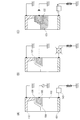
ここで、従来のパワーMISFETについて説明する。図2(A)は従来の単結晶珪素を用いたパワーMISFETの原理を説明するものである。このパワーMISFETは、P型の単結晶珪素基板201上にN型の不純物を拡散して形成したソース202、ドレイン205を有し、それぞれにソース電極206、ドレイン電極207が設けられる。また、基板上にはゲート電極204と層間絶縁物208が設けられる。ソース202とドレイン205の間で、かつ、ゲート電極の下の部分はチャネル形成領域となる。
Here, a conventional power MISFET will be described. FIG. 2A explains the principle of a conventional power MISFET using single crystal silicon. This power MISFET has a
これらの構成要素は通常のMISFETと同じであるが、それらに加えて、このパワーMISFETでは、ドレイン205とチャネル形成領域の間にドリフト領域203が設けられている。この領域は、MISFETがオフとなった際に、MISFETのドレイン205とゲート電極204にかかる高電圧を吸収する目的で設けられる。
These components are the same as those of a normal MISFET. In addition, in this power MISFET, a
すなわち、高電圧が印加された際には、ドリフト領域は空乏化して、絶縁体となり、その領域に珪素の耐圧以下の電界がかかることで、MISFETが破壊されることを防ぐ。珪素の絶縁破壊電界強度は0.3MV/cmなので、3kVの耐圧を保証するMISFETであれば、ドリフト領域の幅X1は100μm必要である。 That is, when a high voltage is applied, the drift region is depleted and becomes an insulator, and an electric field lower than the withstand voltage of silicon is applied to the region, thereby preventing the MISFET from being destroyed. Since the dielectric breakdown field strength of silicon is 0.3 MV / cm, the width X 1 of the drift region needs to be 100 μm in the case of a MISFET that guarantees a breakdown voltage of 3 kV.
一方、MISFETがオンとなった場合には、この領域は導電性を示す必要があるため、N型の導電性を示すことが要求されるが、ドナーの濃度が高すぎると、十分に空乏化できなくなる。ドナー濃度は4×1013cm−3が適正となる。 On the other hand, when the MISFET is turned on, this region needs to show conductivity, and therefore it is required to show N-type conductivity. However, if the donor concentration is too high, the region is sufficiently depleted. become unable. An appropriate donor concentration is 4 × 10 13 cm −3 .
ところで、ドナー濃度が4×1013cm−3である単結晶珪素の抵抗率は100Ωcm以上となる。図2(A)のように基板201の1つの面の浅い部分にドリフト領域203を形成すると、その抵抗が高くなるので、図2(B)のように、基板211のほとんどの部分をドリフト領域213として、電流の流れる断面積を大きくすることにより、その抵抗を下げることがおこなわれている。
By the way, the resistivity of single crystal silicon whose donor concentration is 4 × 10 13 cm −3 is 100 Ωcm or more. When the
一般に耐圧を10倍とするには、ドリフト領域の厚さを10倍にし、ドナー濃度を1/100とすることが求められる。ドナー濃度が1/100となるとドリフト領域の抵抗率は100倍となる。そのため、オン抵抗は1000倍となる。 In general, in order to increase the breakdown voltage by 10 times, it is required to increase the thickness of the drift region by 10 times and the donor concentration to 1/100. When the donor concentration is 1/100, the resistivity of the drift region becomes 100 times. Therefore, the on-resistance is 1000 times.
耐圧3kVを保証するには、ドリフト領域213の厚さX1は100μmあれば十分であるが、現実には、基板211の表面から厚さ100μmの部分のみをドーピングしてドリフト領域とすることは困難であるため、基板211の厚さのほとんど(数百μm)をドリフト領域213として使用する。ドリフト領域213は上述のように抵抗が高く、ドリフト領域213の抵抗は5Ωcm2(電流の断面1cm2あたりの抵抗が5Ωという意味)以上となる。オン状態のMISFETの抵抗はほとんどがドリフト領域のものである。
In order to guarantee a withstand voltage of 3 kV, it is sufficient that the thickness X 1 of the
しかも、このタイプのパワーMISFETは多くのドーピング工程が必要である。すなわち、極めて弱いN型単結晶珪素の基板211の裏面にN型不純物をドーピングして、ドレイン215を形成する。さらに、ゲート電極214を形成した後、表面より、P型不純物をドーピングしてP型領域219とN型不純物をドーピングしてソース212を、それぞれ形成する。ドリフト領域213は基板と同じ不純物濃度である。その後、ソース電極216、ドレイン電極217、層間絶縁物218が設けられる。
Moreover, this type of power MISFET requires many doping steps. That is, the
珪素の場合は100μm以上のドリフト領域が必要であったが、バンドギャップが3電子ボルト以上の酸化物半導体においては絶縁破壊電界強度が3MV/cm以上であるため、ドリフト領域に相当する部分の幅は10μmでよい。一方、珪素半導体ではドリフト領域に微量のドナーを拡散させてオンの際の導電性を制御できるが、通常の酸化物半導体ではそのような技術は確立されていない。 In the case of silicon, a drift region of 100 μm or more was necessary. However, in an oxide semiconductor having a band gap of 3 electron volts or more, the breakdown electric field strength is 3 MV / cm or more, so the width of the portion corresponding to the drift region May be 10 μm. On the other hand, in silicon semiconductors, a small amount of donor can be diffused in the drift region to control the on-state conductivity. However, such techniques have not been established in ordinary oxide semiconductors.
特に、10μm以上もの厚みを有する酸化物半導体にドナーを均質に分散させる技術は十分に研究されていない。加えて、珪素半導体のように均質なドナー濃度を有するウェハー状基板に酸化物半導体を加工する技術も知られていない。 In particular, a technique for uniformly dispersing a donor in an oxide semiconductor having a thickness of 10 μm or more has not been sufficiently studied. In addition, there is no known technique for processing an oxide semiconductor into a wafer-like substrate having a uniform donor concentration such as a silicon semiconductor.
酸化物半導体では水素がドナーとなることは知られている。また、酸素欠損がドナーの要因となることも知られている。しかしながら、本発明者の知見では、水素が酸化物半導体中に存在すると信頼性に大きな問題を生じる。一方、酸素欠損やその他のドナー不純物も含めて、その濃度を精密に制御できるような技術は未だ知られていない。 It is known that hydrogen is a donor in an oxide semiconductor. It is also known that oxygen deficiency causes donors. However, according to the knowledge of the present inventor, if hydrogen is present in an oxide semiconductor, a serious problem occurs in reliability. On the other hand, there is no known technology that can precisely control the concentration of oxygen vacancies and other donor impurities.
また、図2の例では、半導体基板中にN型領域とP型領域を形成することがおこなわれるが、一般に酸化物半導体では、N型領域のみ、あるいはP型領域のみは形成できても、双方を形成することは困難である。したがって、珪素半導体の技術をそのまま酸化物半導体に適用することは非常に難しいといわざるを得ない。 In the example of FIG. 2, an N-type region and a P-type region are formed in a semiconductor substrate. In general, in an oxide semiconductor, only an N-type region or only a P-type region can be formed. It is difficult to form both. Therefore, it can be said that it is very difficult to apply the technique of silicon semiconductor to an oxide semiconductor as it is.
その点に関して、本発明者は酸化物半導体のMISFETの動作を究明した結果、以下に示す構造のMISFETで目的とする耐圧を得られること、およびオンの際に十分な電流が流れることを見出した。また、酸化物半導体はさまざまな基板上に形成できることから放熱性に優れたパワーMISFETを形成できることを見出した。 In this regard, as a result of investigating the operation of an oxide semiconductor MISFET, the present inventor has found that a target breakdown voltage can be obtained with a MISFET having the structure shown below, and that a sufficient current flows when turned on. . It has also been found that a power MISFET having excellent heat dissipation can be formed because an oxide semiconductor can be formed on various substrates.
本発明の一態様は、バンドギャップが3電子ボルト以上である酸化物半導体の耐圧に着目し、これを用いることで、例えば、耐圧3kVでもオン抵抗が5Ωcm2未満、好ましくは1Ωcm2以下という高効率のパワーMISFETを提供するものである。もちろん、これらの具体的な数値は本発明を限定するものではない。 One embodiment of the present invention focuses on the withstand voltage of an oxide semiconductor having a band gap of 3 eV or more, and by using this, for example, the on-resistance is less than 5 Ωcm 2 , preferably 1 Ωcm 2 or less even at a withstand voltage of 3 kV. An efficient power MISFET is provided. Of course, these specific numerical values do not limit the present invention.
また、本発明の一態様は、新規の半導体装置を提供することを課題とする。また、本発明の一態様は、半導体装置の新規な製造方法を提供することを課題とする。また、本発明の一態様は、半導体装置の新規な駆動方法を提供することを課題とする。 Another object of one embodiment of the present invention is to provide a novel semiconductor device. Another object of one embodiment of the present invention is to provide a novel method for manufacturing a semiconductor device. Another object of one embodiment of the present invention is to provide a novel driving method of a semiconductor device.
本発明の態様の一は、第1の酸化物半導体層と、第1の酸化物半導体層との間に第1の絶縁層を挟んで形成された第1の電極と、第1の電極の側面との間に第2の絶縁層を挟んで形成され、第1の酸化物半導体層と接する第2の酸化物半導体層と、第2の酸化物半導体層に接して設けられた第2の電極と、第1の酸化物半導体層に接して設けられた第3の電極を有し、第1の絶縁層と第3の電極との距離が、第2の絶縁層と第3の絶縁層との間の距離より大きいパワーMISFETである。 According to one embodiment of the present invention, a first oxide semiconductor layer, a first electrode formed by sandwiching a first insulating layer between the first oxide semiconductor layer, a first electrode And a second oxide semiconductor layer in contact with the first oxide semiconductor layer and a second oxide semiconductor layer provided in contact with the second oxide semiconductor layer. An electrode and a third electrode provided in contact with the first oxide semiconductor layer, and the distance between the first insulating layer and the third electrode is determined by the second insulating layer and the third insulating layer; The power MISFET is larger than the distance between the two.
本発明の態様の一は、空孔を有する平板状の第1の電極と、第1の電極の一面に対向して設けられた第1の酸化物半導体層と、第1の電極の空孔の側面に隣接して設けられ、第1の酸化物半導体層と第1の電極の空孔で接する第2の酸化物半導体層を有し、第1の電極と第1の酸化物半導体層との間、および第1の電極と第2の酸化物半導体層との間には絶縁層が設けられ、第1の酸化物半導体層は第2の酸化物半導体層より厚いパワーMISFETである。 According to one embodiment of the present invention, a flat plate-like first electrode having holes, a first oxide semiconductor layer provided to face one surface of the first electrode, and holes in the first electrode The second oxide semiconductor layer is provided adjacent to the side surface of the first oxide semiconductor layer and is in contact with the first oxide semiconductor layer through the holes of the first electrode. The first electrode, the first oxide semiconductor layer, And an insulating layer is provided between the first electrode and the second oxide semiconductor layer, and the first oxide semiconductor layer is a power MISFET thicker than the second oxide semiconductor layer.
本発明の態様の一は、平板状の第1の酸化物半導体層と、第1の酸化物半導体層の一面に絶縁して設けられた第1の電極と、第1の電極の側面を覆い、絶縁して設けられた膜状の第2の酸化物半導体層と、第2の酸化物半導体層に接して設けられた第2の電極と、第1の酸化物半導体層の他の面に接して設けられた第3の電極とを有し、第1の酸化物半導体層と第2の酸化物半導体層は接し、第1の酸化物半導体層は第2の酸化物半導体層より厚いパワーMISFETである。 One embodiment of the present invention covers a flat plate-like first oxide semiconductor layer, a first electrode provided on one surface of the first oxide semiconductor layer, and a side surface of the first electrode. An insulating film-like second oxide semiconductor layer; a second electrode provided in contact with the second oxide semiconductor layer; and the other surface of the first oxide semiconductor layer. The first oxide semiconductor layer and the second oxide semiconductor layer are in contact with each other, and the first oxide semiconductor layer is thicker than the second oxide semiconductor layer. MISFET.
上記において、第2の酸化物半導体層を覆って絶縁物が設けられ、絶縁物に形成された開口部を介して第2の酸化物半導体層と第2の電極が接する構成としてもよい。その際、開口部は第1の電極と重なるように設けられてもよい。 In the above structure, an insulator may be provided so as to cover the second oxide semiconductor layer, and the second oxide semiconductor layer and the second electrode may be in contact with each other through an opening formed in the insulator. In that case, the opening may be provided so as to overlap with the first electrode.
なお、上記において、第1の酸化物半導体層は絶縁体、P型単結晶珪素あるいはN型単結晶珪素、導電体のいずれかを基板として、その上に形成されてもよい。また、第1の電極乃至第3の電極は金属あるいは導電性酸化物、導電性窒化物よりなるものを用いてもよい。 Note that in the above, the first oxide semiconductor layer may be formed over any of an insulator, P-type single crystal silicon, N-type single crystal silicon, and a conductor as a substrate. Alternatively, the first to third electrodes may be made of metal, conductive oxide, or conductive nitride.
このようなパワーMISFETの第2の電極と第3の電極の間に500V以上の電源と負荷を直列に接続し、第1の電極に制御用の信号を入力して使用する。すなわち、第1の電極がゲート電極、第2の電極がソース電極、第3の電極がドレイン電極として機能する。 A power supply of 500 V or higher and a load are connected in series between the second electrode and the third electrode of such a power MISFET, and a control signal is input to the first electrode for use. That is, the first electrode functions as a gate electrode, the second electrode functions as a source electrode, and the third electrode functions as a drain electrode.
また、第1の酸化物半導体層中のドナーあるいはアクセプタに由来するキャリア濃度は1×1012cm−3以下、好ましくは1×1011cm−3以下としてもよい。本明細書ではキャリア濃度が1×1012cm−3以下の半導体をI型半導体ともいう。 The carrier concentration derived from the donor or acceptor in the first oxide semiconductor layer may be 1 × 10 12 cm −3 or less, preferably 1 × 10 11 cm −3 or less. In this specification, a semiconductor with a carrier concentration of 1 × 10 12 cm −3 or less is also referred to as an I-type semiconductor.
なお、酸化物半導体は導体に接すると、後述のように、導体からキャリアが注入されたり、導体にキャリアが吸収されたりして、ドナーあるいはアクセプタに由来するキャリア濃度を知ることは困難である。 Note that when an oxide semiconductor is in contact with a conductor, as described later, carriers are injected from the conductor or carriers are absorbed by the conductor, so that it is difficult to know the carrier concentration derived from the donor or the acceptor.
したがって、現実的にはMISFET内の酸化物半導体層のドナーあるいはアクセプタに由来するキャリア濃度を知ることは困難である。その場合には、MISFETに使用されている酸化物半導体層と同じ方法で作製された酸化物半導体層の、導体から10μm以上、好ましくは100μm以上離れた点で測定することで、1×1012cm−3以下であるか否かを知ることができる。 Therefore, in reality, it is difficult to know the carrier concentration derived from the donor or acceptor of the oxide semiconductor layer in the MISFET. In that case, the oxide semiconductor layer manufactured by the same method as the oxide semiconductor layer used for the MISFET is measured at a point away from the conductor by 10 μm or more, preferably 100 μm or more, thereby 1 × 10 12. It is possible to know whether it is cm −3 or less.
上記に関連して、酸化物半導体層は、酸素欠損濃度や水素濃度が小さい方が好ましい。酸素欠損や水素の混入はキャリアの源泉となるためである。また、水素を含有すると、MISFETの動作を不安定にする。水素濃度は1×1018cm−3以下とすることが好ましい。 In relation to the above, the oxide semiconductor layer preferably has a lower oxygen deficiency concentration or hydrogen concentration. This is because oxygen vacancies and hydrogen contamination are sources of carriers. Moreover, when hydrogen is contained, the operation of the MISFET becomes unstable. The hydrogen concentration is preferably 1 × 10 18 cm −3 or less.
また、第2の電極(あるいは第3の電極)の仕事関数は、第2の酸化物半導体層(あるいは第1の酸化物半導体層)の電子親和力と0.3電子ボルトの和(すなわち、電子親和力+0.3電子ボルト)よりも小さいことが好ましい。あるいは、第2の電極(あるいは第3の電極)と第2の酸化物半導体層(あるいは第1の酸化物半導体層)の接合はオーミック接合であることが好ましい。また、第3の電極の仕事関数は第2の電極の仕事関数よりも大きいことが好ましい。 The work function of the second electrode (or the third electrode) is the sum of the electron affinity of the second oxide semiconductor layer (or the first oxide semiconductor layer) and 0.3 electron volt (that is, the electron Affinity +0.3 eV) is preferable. Alternatively, the junction between the second electrode (or the third electrode) and the second oxide semiconductor layer (or the first oxide semiconductor layer) is preferably an ohmic junction. The work function of the third electrode is preferably larger than the work function of the second electrode.
さらには、第1の電極の仕事関数が、第2の電極(あるいは第3の電極)の仕事関数より0.3電子ボルト以上大きいとよい。あるいは、第1の電極の仕事関数は、第1の酸化物半導体層(あるいは第2の酸化物半導体層)の電子親和力と0.6電子ボルトの和(すなわち、電子親和力+0.6電子ボルト)よりも大きいことが好ましい。 Furthermore, the work function of the first electrode is preferably 0.3 electron volts or more larger than the work function of the second electrode (or the third electrode). Alternatively, the work function of the first electrode is the sum of the electron affinity of the first oxide semiconductor layer (or the second oxide semiconductor layer) and 0.6 electron volts (that is, electron affinity + 0.6 electron volts). Is preferably larger.
なお、例えば、半導体層に厚さが数nm以下の極めて薄い第1の導体層と、それに重なる、ある程度の厚みのある第2の導体層が積層している場合は、第1の導体層の仕事関数の影響がかなり低下する。それは、ゲート電極のように間に絶縁層を有する電極においても同様である。したがって、本発明を適用するに当たっては、界面から5nm離れた部分での各種材料の仕事関数が、本発明で好ましいとする条件を満たすように設計してもよい。 For example, when a very thin first conductor layer having a thickness of several nanometers or less and a second conductor layer having a certain thickness are stacked on the semiconductor layer, the first conductor layer The effect of work function is considerably reduced. The same applies to an electrode having an insulating layer in between, such as a gate electrode. Therefore, when applying the present invention, the work functions of various materials at a portion 5 nm away from the interface may be designed so as to satisfy the conditions that are preferable in the present invention.
後述の説明から明らかなように、本発明の一態様のパワーMISFETは十分な耐圧と低いオン抵抗を有する。特に本発明のパワーMISFETは、公知の珪素半導体のパワーMISFETと異なり、ドーピングによりN型領域やP型領域を形成する必要がない。そのことにより製造工程を短縮することができる。 As will be apparent from the following description, the power MISFET of one embodiment of the present invention has a sufficient breakdown voltage and a low on-resistance. In particular, the power MISFET of the present invention does not need to form an N-type region or a P-type region by doping, unlike a known silicon MISFET. As a result, the manufacturing process can be shortened.
本発明の一態様は、キャリアとして、実質的に、電子あるいはホールの一方しか用いられない半導体材料において効果が顕著である。すなわち、電子あるいはホールの一方の移動度が、1cm2/Vs以上であるのに対し、他方の移動度が0.01cm2/Vs以下であるとか、他方がキャリアとして存在しないとか、あるいは、一方の有効質量が他方の100倍以上であるとか、という場合においても、本発明の一態様においては、十分に機能するパワーMISFETが得られる。 One embodiment of the present invention has a remarkable effect in a semiconductor material in which only one of electrons and holes is substantially used as a carrier. That is, the mobility of one of electrons or holes is 1 cm 2 / Vs or more, while the other mobility is 0.01 cm 2 / Vs or less, or the other does not exist as a carrier, Even in the case where the effective mass is 100 times or more of the other, in one embodiment of the present invention, a sufficiently functioning power MISFET can be obtained.
以下、実施の形態について図面を参照しながら説明する。但し、実施の形態は多くの異なる態様で実施することが可能であり、趣旨及びその範囲から逸脱することなくその形態及び詳細を様々に変更し得ることは当業者であれば容易に理解される。従って本実施の形態の記載内容に限定して解釈されるものではない。なお、以下に説明する構成において、同様のものを指す符号は異なる図面間で共通の符号を用いて示し、同一部分又は同様な機能を有する部分の詳細な説明は省略することがある。 Hereinafter, embodiments will be described with reference to the drawings. However, the embodiments can be implemented in many different modes, and it is easily understood by those skilled in the art that the modes and details can be variously changed without departing from the spirit and scope thereof. . Therefore, the present invention is not construed as being limited to the description of this embodiment mode. Note that in the structures described below, the same components are denoted by the same reference numerals in different drawings, and detailed description of the same portions or portions having similar functions may be omitted.
(実施の形態1)
図1(A)にパワーMISFETの例を示す。このパワーMISFETは、基板101上に設けられた層状のドレイン電極102と、酸化物半導体よりなる厚さX1の平板状のI型の半導体層103と、高さX2、幅X3、テーパー角αのゲート電極105と、ゲート電極105を覆って形成された、酸化物半導体よりなる膜状のI型の半導体層109とを有する。
(Embodiment 1)
FIG. 1A shows an example of a power MISFET. This power MISFET includes a
また、ゲート電極105と半導体層103の間、ゲート電極105と半導体層109の間には絶縁層104が設けられており、絶縁層104はゲート絶縁膜として機能する。さらに、半導体層109を覆って層間絶縁物111が設けられ、層間絶縁物111に設けられた開口部を介して、ソース電極112が半導体層109と接する。
An insulating
図1(B)に、この半導体装置の回路を示す。ここで、半導体層103の厚さX1はこのパワーMISFETの耐圧を決定する上で重要な要素であり、例えば、半導体層103に用いる酸化物半導体を後述するIn−Ga−Zn系酸化物とし、耐圧を3kVとするのであれば10μmとするとよい。
FIG. 1B shows a circuit of this semiconductor device. The thickness X 1 of the
また、このMISFETでは半導体層109にチャネルが形成される。このMISFETのチャネル長は、主としてゲート電極105の上面および側面の長さで決定される。チャネル長が半導体層109の厚さに比べて十分に長くないと、短チャネル効果により、オフの際のリーク電流が十分に小さくならない。一方でチャネル長が長いと、オン電流が減少する。
In this MISFET, a channel is formed in the
一般に、PN接合を用いないFETでは、チャネル長に比較してチャネル部分の半導体層の厚さが大きくなると、オフの際のリーク電流が大きくなる。この効果は半導体層の厚さだけではなくゲート絶縁膜の実効的な厚さ(ゲート絶縁膜の物理的な厚さ×半導体層の比誘電率/ゲート絶縁膜の比誘電率)とも関連する。 In general, in an FET that does not use a PN junction, when the thickness of the semiconductor layer in the channel portion is larger than the channel length, the leakage current at the time of off increases. This effect is related not only to the thickness of the semiconductor layer but also to the effective thickness of the gate insulating film (physical thickness of the gate insulating film × relative permittivity of the semiconductor layer / relative permittivity of the gate insulating film).
チャネル部分の半導体層の厚さとゲート絶縁膜の実効的な厚さの和がチャネル長の1/2以上であるとしきい値が低下し、また、サブスレショールド特性も悪化する。すなわち、オフの際のソース電極とドレイン電極の間の電流が増加する。図1に示すMISFETがそのような状態にあると、オフの際に絶縁層104に高い電圧がかかって、パワーMISFETが破壊されてしまう。
When the sum of the thickness of the semiconductor layer in the channel portion and the effective thickness of the gate insulating film is ½ or more of the channel length, the threshold value is lowered, and the subthreshold characteristic is also deteriorated. That is, the current between the source electrode and the drain electrode when turned off increases. When the MISFET shown in FIG. 1 is in such a state, a high voltage is applied to the insulating
詳細については省略するが、チャネル部分の半導体層の厚さとゲート絶縁膜の実効的な厚さの和は、チャネル長の1/3以下、好ましくは1/5以下とするとよい。このように半導体層109の厚さは半導体層103の厚さに比べると極めて小さく、通常は、半導体層103の厚さは半導体層109の厚さの100倍以上となる。
Although the details are omitted, the sum of the thickness of the semiconductor layer in the channel portion and the effective thickness of the gate insulating film may be 1/3 or less, preferably 1/5 or less of the channel length. As described above, the thickness of the
また、テーパー角αが大きい(垂直に近くなる)とゲート電極105の側面に半導体層109を形成することが困難となるが、逆に、テーパー角αが小さい(水平に近くなる)とMISFETを形成するのに多くの面積が必要である。したがって、半導体層109の厚さおよびゲート電極105の厚さX2、テーパー角αには好ましい値がある。
If the taper angle α is large (close to the vertical), it becomes difficult to form the
一般に半導体層109とゲート電極105にかかる最大の電圧は、50V未満であるので、それに耐えられる程度に設計するとよい。例えば、半導体層の厚さを5nm以上30nm以下、ゲート電極105の高さX2を0.5μm以上10μm以下、テーパー角αを30°以上90°以下とするとよい。特に、製造工程とMISFETの形成面積を考慮すると、テーパー角αを40°以上70°以下とするとよい。
In general, the maximum voltage applied to the
例えば、ゲート電極105にかかる電圧が30Vであるとすると、絶縁層104の厚さは、酸化珪素を用いた場合に100nm以上が必要である。この際、半導体層109の厚さを30nmとすると、十分なオフ特性を得るには、チャネル長は2μm以上であることが好ましい。ゲート電極105の側面の長さを2μmとするには、テーパー角αを60°とすると、ゲート電極105の高さX2を約1.73μmとすればよい。
For example, if the voltage applied to the
このような構造のパワーMISFETの動作について説明する。パワーMISFETは、図4(A)に示すようにソース電極112は接地し、ドレイン電極102には負荷113と高電圧電源を直列に接続する。ドレイン電極102には正の電圧がかかるように接続する。また、ゲート電極105にはMISFETをオンオフさせるための信号が与えられる。なお、負荷は単なる抵抗に限られず、インダクター、トランス、トランジスタ(パワーMISFETを含む)等でもよい。
The operation of the power MISFET having such a structure will be described. In the power MISFET, as shown in FIG. 4A, the
酸化物半導体、特に亜鉛もしくはインジウムを有する酸化物半導体においては、これまで、P型の導電性を示すものはほとんど報告されていない。そのため、珪素のFETのようなPN接合を用いたものは報告されておらず、特許文献1および特許文献2にあるように、N型の酸化物半導体に導体電極を接触させた導体半導体接合によって、ソース、ドレインを形成していた。 Until now, oxide semiconductors, particularly oxide semiconductors containing zinc or indium, have hardly been reported to exhibit P-type conductivity. Therefore, there is no report using a PN junction such as a silicon FET, and as disclosed in Patent Document 1 and Patent Document 2, a conductor semiconductor junction in which a conductor electrode is brought into contact with an N-type oxide semiconductor. The source and drain were formed.
さらにドナーを減らして、それに由来するキャリア濃度を低減させたI型の酸化物半導体では、信頼性も高く、かつ、オンオフ比が大きく、また、サブスレショールド値が小さなMISFETが得られる(特許文献3参照)。そして、このようなドナー濃度の低い酸化物半導体を用いたMISFETの動作について以下のように考察される。 In addition, an I-type oxide semiconductor in which the number of donors is reduced and the carrier concentration derived therefrom is reduced can provide a MISFET with high reliability, a large on / off ratio, and a small subthreshold value (Patent Literature). 3). Then, the operation of the MISFET using such an oxide semiconductor having a low donor concentration is considered as follows.
導体半導体接合によって、ソース、ドレインを形成したMISFETでは、用いる半導体のキャリア濃度が高いと、オフ状態でもソースとドレインの間に電流(オフ電流)が流れてしまう。そこで、半導体中のキャリア濃度を低減させて、I型とすることにより、オフ電流を低減できる。 In a MISFET in which a source and a drain are formed by a conductor semiconductor junction, if the carrier concentration of the semiconductor used is high, a current (off-state current) flows between the source and the drain even in the off state. Thus, the off-state current can be reduced by reducing the carrier concentration in the semiconductor to be I-type.
一般に、導体半導体接合においては、導体の仕事関数と半導体の電子親和力(あるいはフェルミ準位)の関係によって、オーミック接合になったり、ショットキーバリヤ接合になったりする。例えば、電子親和力が4.3電子ボルトの半導体に、仕事関数3.9電子ボルトの導体を接触させ、理想的な(すなわち、接合界面での化学反応やキャリアのトラップのない状態)導体半導体接合を形成したとすると、導体から半導体の一定の幅を有する領域へ電子が流入する。 In general, in a conductor semiconductor junction, an ohmic junction or a Schottky barrier junction is formed depending on the relationship between the work function of the conductor and the electron affinity (or Fermi level) of the semiconductor. For example, a conductor having a work function of 3.9 eV is brought into contact with a semiconductor having an electron affinity of 4.3 eV, and an ideal (ie, no chemical reaction or carrier trap at the bonding interface) conductor semiconductor junction If electrons are formed, electrons flow from a conductor into a region having a certain width of a semiconductor.
その場合、導体と半導体の接合界面に近いほど電子の濃度が高く、電子濃度は、大雑把な計算では、導体半導体接合界面から数nmでは1×1020cm−3、数十nmでは1×1018cm−3、数百nmでは1×1016cm−3、数μmでも1×1014cm−3である。すなわち、半導体自体がI型であっても、導体との接触によって、電子濃度の高い領域ができてしまう。このような電子の多い領域が導体半導体接合界面近傍にできることにより、導体半導体接合はオーミック接合となる。 In that case, the closer to the conductor-semiconductor junction interface, the higher the concentration of electrons, and the rough calculation shows that the electron concentration is 1 × 10 20 cm −3 at several nm from the conductor-semiconductor junction interface and 1 × 10 at several tens of nm. 18 cm −3 , 1 × 10 16 cm −3 at several hundred nm, and 1 × 10 14 cm −3 even at several μm. That is, even if the semiconductor itself is I-type, a region having a high electron concentration is formed by contact with the conductor. By forming such a region with many electrons in the vicinity of the conductor semiconductor junction interface, the conductor semiconductor junction becomes an ohmic junction.
一方、例えば、電子親和力が4.3電子ボルトの半導体に、仕事関数4.9電子ボルトの導体を接触させ、理想的な導体半導体接合を形成したとすると、半導体のある幅の領域に存在する電子が導体へ移動する。電子がなくなった領域では、当然のことながら、電子の濃度は極めて低くなる。電子が移動する半導体の領域の幅は、半導体の電子濃度に依存し、例えば、もともとの半導体の電子濃度が1×1018cm−3であれば、数十nm程度である。 On the other hand, for example, if a semiconductor having a work affinity of 4.9 eV is brought into contact with a semiconductor having an electron affinity of 4.3 eV and an ideal conductor semiconductor junction is formed, the semiconductor exists in a certain width region of the semiconductor. Electrons move to the conductor. In the region where the electrons have disappeared, the electron concentration is naturally very low. The width of the semiconductor region in which electrons move depends on the electron concentration of the semiconductor. For example, if the electron concentration of the original semiconductor is 1 × 10 18 cm −3 , it is about several tens of nm.
そして、この部分の電子濃度が著しく低くなるため、バンド図においては、導体と半導体との接合界面において、バリヤができる。このようなバリヤを有する導体半導体接合をショットキーバリヤ型接合という。電子は、半導体から導体へは流れやすいが、導体から半導体へは、バリヤがあるため流れにくい。したがって、ショットキーバリヤ型接合では整流作用が観測される。 And since the electron concentration of this part becomes remarkably low, in a band figure, a barrier is made in the junction interface of a conductor and a semiconductor. A conductor semiconductor junction having such a barrier is called a Schottky barrier junction. Electrons tend to flow from the semiconductor to the conductor, but are difficult to flow from the conductor to the semiconductor due to a barrier. Therefore, a rectifying action is observed in the Schottky barrier type junction.
同様のことは、導体が直接、半導体に接していなくても起こる。例えば、半導体と導体との間に絶縁膜が存在する場合にも半導体の電子濃度は導体の影響を受ける。もちろん、その程度は、絶縁膜の厚さや誘電率により影響される。絶縁膜が厚くなるか、誘電率が低くなれば、導体の影響は小さくなる。 The same thing happens even if the conductor is not in direct contact with the semiconductor. For example, even when an insulating film exists between a semiconductor and a conductor, the electron concentration of the semiconductor is affected by the conductor. Of course, the degree is influenced by the thickness and dielectric constant of the insulating film. If the insulating film becomes thicker or the dielectric constant becomes lower, the influence of the conductor becomes smaller.
ソース電極と半導体あるいはドレイン電極と半導体との接合は、電流が流れやすいことが好ましいので、オーミック接合となるように導体材料が選択される。例えば、チタンや窒化チタン等である。電極と半導体との接合がオーミック接合であると、得られるMISFETの特性が安定し、良品率が高くなる。 The junction between the source electrode and the semiconductor or the drain electrode and the semiconductor is preferably such that an electric current easily flows. Therefore, the conductor material is selected so as to form an ohmic junction. For example, titanium or titanium nitride. When the junction between the electrode and the semiconductor is an ohmic junction, the characteristics of the obtained MISFET are stabilized and the yield rate is increased.
また、ゲート電極の材料としては、半導体の電子を排除する作用を有する材料が選択される。例えば、ニッケルや白金等である。あるいは、酸化モリブデン等の導電性酸化物でもよい。導電性酸化物のいくつかは仕事関数が5電子ボルト以上である。このような材料は導電性に劣ることがあるので、導電性のよい材料との積層によって使用するとよい。また、窒化インジウム、窒化亜鉛等の導電性窒化物もやはり仕事関数が5電子ボルト以上であるので好ましい。 As the material for the gate electrode, a material having an action of eliminating semiconductor electrons is selected. For example, nickel or platinum. Alternatively, a conductive oxide such as molybdenum oxide may be used. Some of the conductive oxides have a work function of 5 electron volts or more. Since such a material may be inferior in conductivity, it may be used by stacking with a material having good conductivity. Conductive nitrides such as indium nitride and zinc nitride are also preferable because the work function is 5 electron volts or more.
上述のように、導体との接触によって電子が半導体層に侵入することが示されたが、例えば、図1(A)のパワーMISFETのようにドリフト領域に相当する半導体層103の厚さX1が10μmであれば、ソース電極112とドレイン電極102に電位差が無い場合には、半導体層103の平均の電子濃度は2×1013cm−3程度と見積もられる。この値は図2(A)に示す耐圧3kVの従来のパワーMISFETのドリフト領域203あるいは図2(B)に示すドリフト領域213のドナー濃度と同じレベルである。
As described above, it has been shown that electrons enter the semiconductor layer by contact with the conductor. For example, the thickness X 1 of the
図4(B)にオフ状態のパワーMISFETの電子状態を模式的に示す。オフ状態の場合には、オーミック接触しているソース電極112からは半導体層109に電子が流入しようとするが、仕事関数の高いゲート電極105(0Vに保持されている)により押し込められる。図4(B)に示すようにソース電極112近傍にのみ電子濃度の高い領域121が形成されるが、それ以外の領域には拡散しない。このため、電子濃度の高い領域121以外の領域は極めて抵抗の高い状態となる。
FIG. 4B schematically shows the electronic state of the power MISFET in the off state. In the off state, electrons try to flow into the
ソース電極112から半導体層103へ電子が供給されないので、半導体層103は容易に空乏化し、ドレイン電極102とゲート電極105にかかる電圧はこの空乏化した半導体層103で吸収することとなる。半導体層103はその電圧に耐えられる厚さで設計されているので、MISFETが破壊されることはない。空乏化した半導体層103は極めて高い抵抗を呈し、負荷113にはほとんど電流が流れない。
Since electrons are not supplied from the
図4(B)では、ゲート電極105の電圧を0Vとしたが、よりオフ特性を高めるために適切な負の電位としてもよい。
In FIG. 4B, the voltage of the
図4(C)にはオン状態のパワーMISFETの電子状態を模式的に示す。ゲート電極105は正の電圧に保たれるので、その周囲の半導体層109および半導体層103には極めて電子濃度の高い領域122と比較的電子濃度の高い領域123が形成される。この結果、半導体層109にはチャネルが形成され、ソース電極112からの電子が半導体層103に到達することができる。
FIG. 4C schematically shows an electronic state of the power MISFET in the on state. Since the
ここで、注目すべきは、半導体層103においても、極めて電子濃度の高い領域122と比較的電子濃度の高い領域123が形成されることである。これはゲート電極105が正の電圧に保持されていることによるものである。
Here, it should be noted that also in the
半導体層103の平均の電子濃度は、ゲート電極105の電圧に依存するが、ゲート電極105の電圧が10Vであれば2×1014cm−3程度となる。上記のように、ゲート電極105の寄与を無視した状態で、ドレイン電極102の電圧が0Vであれば、半導体層103の平均の電子濃度は2×1013cm−3程度であるが、その場合と比較すると明らかに半導体層103の抵抗が低下する。
The average electron concentration of the
なお、同様な効果は図2(B)に示す従来のパワーMISFETでも起こるのであるが、この場合には、ドリフト領域213の厚さX1は100μm以上が必要とされるので、ゲート電極214によって、ドリフト領域213に誘起される平均の電子濃度は最大でも2×1012cm−3程度であり、ドリフト領域213のドナーによる電子濃度(4×1013cm−3程度)よりもはるかに小さく、効果はほとんど観測されない。
A similar effect also occurs in the conventional power MISFET shown in FIG. 2B, but in this case, the thickness X 1 of the
なお、ドレイン電極102の材料として仕事関数のより低い材料を用いると、ドレイン電極102から半導体層103により多くの電子を供給できるため、半導体層103の抵抗を低減する上で好ましい。ドレイン電極102から半導体層103に供給される電子は、ドレイン電極102の電圧が数ボルトより高くなると、ドレイン電極102に吸収されるので、オフ状態において、半導体層103が空乏化する障害とはならない。
Note that it is preferable to use a material having a lower work function as the material of the
仕事関数の低い材料として、十分に電子濃度の高いN型の窒化ガリウムあるいはN型の酸化ガリウムを用いてもよい。これらは仕事関数が3.5電子ボルト程度であり、導電性を有する。また、これらを構成するガリウムは酸化物半導体でも使用されるものであり、特に半導体層103がガリウムを有する酸化物で作製される場合には、界面での不連続性を避けることができ、製品の歩留まりや特性のばらつきを抑制できる。
As a material having a low work function, N-type gallium nitride or N-type gallium oxide having a sufficiently high electron concentration may be used. These have a work function of about 3.5 electron volts and have conductivity. In addition, gallium constituting them is also used in oxide semiconductors, and in particular, when the
一方、ソース電極112に関しては、特にオフ状態において、その近傍の電子濃度が高いことは、耐圧を低下させる要因となる。したがって、ソース電極112の材料としては、ドレイン電極102の材料よりも仕事関数の大きなものを用いることが好ましい。
On the other hand, regarding the
もし、ゲート電極105の仕事関数が十分に大きくない場合には、ソース電極112近傍の電子濃度の高い領域121がドレイン電極102側へ拡大し、多少なりとも電子がソース電極112からドレイン電極102に流れる。その場合には、絶縁層104に高電圧がかかって、素子が破壊されてしまうおそれがある。そのため、ゲート電極105の仕事関数の値は重要である。
If the work function of the
なお、従来の珪素半導体を用いたパワーMISFETでは、ソース202(あるいはソース212)とチャネル形成領域との間の逆方向のPN接合により同様な作用を得ている。酸化物半導体ではPN接合を用いることができないので、ゲート電極105として仕事関数の大きな材料を用いるとよい。または、オフの状態では、ゲート電極105をソース電極112よりも1ボルト以上電位の低い状態とすることが好ましい。
Note that in a power MISFET using a conventional silicon semiconductor, a similar effect is obtained by a reverse PN junction between the source 202 (or the source 212) and the channel formation region. Since a PN junction cannot be used for an oxide semiconductor, a material having a high work function is preferably used for the
以上の考察から明らかなように、図1(A)に示すMISFETの耐圧は十分である。加えて、ドリフト領域に相当する部分の厚さが珪素半導体の場合の1/10であることによりオン抵抗を低減できる。 As is clear from the above consideration, the breakdown voltage of the MISFET shown in FIG. In addition, since the thickness of the portion corresponding to the drift region is 1/10 that of a silicon semiconductor, the on-resistance can be reduced.
図1(A)のMISFETは、1つのゲート電極105が示されているが、半導体層103上に同様なゲート電極を複数形成するとよい。例えば、空孔が複数設けられた平板状の導電体をゲート電極105として用いてもよい。図3(A)乃至図3(C)には、その例を示す。
In the MISFET in FIG. 1A, one
図3(A)は、平板状の導電体に正方形の空孔を設けたものをゲート電極105とするものである。このゲート電極は半導体層103上に形成され、その上には、半導体層109が空孔を埋めるように形成される。空孔では半導体層109と半導体層103が接するようにする。ゲート電極105と重なる位置にソース電極112が半導体層109と接する場所を設けるとよい。断面は図1(A)に示すものと同様なものとなる。
FIG. 3A shows a
試算では、図1(A)のタイプのMISFETでゲート電極105の高さX2を1.73μm、テーパー角αを60°(つまりチャネル長2μm)、ゲート電極105に形成する空孔の底面の一辺の長さX4を2μm、空孔の間隔(つまりゲート電極105の幅X3)を2μmとすると、1cm角に形成される空孔の数は625万である。
In the trial calculation, in the MISFET of the type shown in FIG. 1A, the height X 2 of the
この空孔の外周がチャネル幅であるので、空孔1つあたりチャネル幅は8μmであり、1cm角に形成されるパワーMISFETのチャネル幅はその625万倍の50mとなる。チャネル長が2μm、チャネル幅が1μm、ゲート絶縁物が厚さ100nmの酸化珪素、半導体層の移動度が10cm2/VsであるMISFETのゲート電極の電圧を10Vとしたときのオン抵抗は2MΩ以下であると計算される。上記の多数の空孔に形成されるMISFETはチャネル幅が50mであるのでオン抵抗は40mΩ以下となる。 Since the outer periphery of this hole is the channel width, the channel width per hole is 8 μm, and the channel width of the power MISFET formed in a 1 cm square is 50.25 times that of 6.25 million. On-resistance is 2 MΩ or less when the gate electrode voltage of a MISFET having a channel length of 2 μm, a channel width of 1 μm, a gate insulator of 100 nm thickness, and a semiconductor layer mobility of 10 cm 2 / Vs is 10 V Is calculated to be Since the MISFET formed in the above-described many holes has a channel width of 50 m, the on-resistance is 40 mΩ or less.
なお、パワーMISFETにおいては、ドリフト領域に相当する半導体層103の抵抗を考慮しなければならない。オン状態での1cm角の半導体層103の抵抗は、半導体層103の移動度を10cm2/Vsとするとき、3Ω程度であり上記の抵抗に比較すると十分に大きく、パワーMISFETの抵抗のほとんどが、半導体層103によるものであることがわかる。もちろん、移動度が増加すると半導体層103の抵抗は低減できる。
In the power MISFET, the resistance of the
ゲート電極105に設ける空孔の形状は、正方形に限られず、図3(B)に示すように円形であっても、図3(C)に示すように矩形であってもよい。その他の形状であってもよい。空孔の占める比率が小さくなると、ゲート電極105の抵抗は低下するが、ゲート電極105とドレイン電極102との間の容量(図1(B)においてC2で示される)が増加する。また、空孔の外周が大きいほどチャネル幅が増加するが、上記のように半導体層103の抵抗が支配的である場合には、チャネル幅を増大させることによるメリットは少ない。
The shape of the holes provided in the
なお、図1(B)に示されるように、このパワーMISFETでは、ソース電極112とゲート電極105の間に容量C1が生じる。容量C1が小さいほど、パワーMISFETはより高速で動作できる。容量C1は主として、ソース電極112が半導体層109と接する部分とゲート電極105との間で形成されるので、この部分の面積(あるいは、接触する部分の個数)を減らすと、容量C1を低減できる。
As shown in FIG. 1B, in this power MISFET, a capacitance C 1 is generated between the
一方、ソース電極112が半導体層109と接する部分の面積を減らすと、この部分の接触抵抗が増大するので、ソース電極の直列抵抗が増大するという別の問題もあるので、ソース電極112が半導体層109と接する部分の面積や個数はこれらの要因を勘案して決定するとよい。
On the other hand, if the area of the portion where the
なお、基板101は絶縁体でも半導体でも導電体でもよいが、熱伝導率の高い材料であることが好ましい。また、基板101を導電体で構成する場合には、ドレイン電極102に相当する部材を基板101で代用することもできる。酸化物半導体の形成に要する温度は600℃以下であるため、さまざまな材料を基板101として用いることができる。そのため、放熱性に優れたパワーMISFETを得ることができる。
Note that the
パワーMISFETが過剰に発熱しないことは安定した特性を得るために必要なことである。一般にMISFETは高い温度で使用されるとオフ電流が増加する。パワーMISFETにおいては、オフ電流が増加すると、回路の破壊につながるため、過剰な発熱は極力避けるべきことである。 It is necessary for the power MISFET not to generate excessive heat in order to obtain stable characteristics. In general, when the MISFET is used at a high temperature, the off-current increases. In a power MISFET, an increase in off-current leads to circuit destruction, so excessive heat generation should be avoided as much as possible.
従来のパワーMISFETでは、基板に相当な厚みのシリコンを用いるため放熱は制約されており、上記のように熱伝導性のよい基板と適切な厚さの半導体層とを近接させることにより効率的に放熱を図ることは、従来のパワーMISFETでは技術的に困難であった。 In conventional power MISFETs, heat dissipation is limited because silicon with a considerable thickness is used for the substrate. As described above, a substrate with good thermal conductivity and a semiconductor layer with an appropriate thickness can be efficiently used. It is technically difficult to dissipate heat with a conventional power MISFET.
例えば、基板101に熱伝導率の高い銅を用い、ドレイン電極を厚さ100nm乃至1μmの窒化チタンで構成してもよい。なお、放熱性を高める観点からは、ソース電極112に重ねて、熱伝導率の高い絶縁体あるいは導電体を用いてもよい。例えば、ソース電極112に重ねて、厚さ1μm乃至10μmの銅の層を形成してもよい。
For example, copper having high thermal conductivity may be used for the
なお、以上の考察では、半導体層103、半導体層109をI型の半導体であるとして、説明した。十分なオフ抵抗を得るため、パワーMISFETの半導体層109(特にチャネルが形成される部分)はI型であることが好ましいが、ドリフト領域に相当する半導体層109では、必ずしもI型である必要はなく、必要とされる耐圧に応じて決定されるキャリア濃度の上限以下のドナー(あるいはアクセプタ)に由来するキャリアを含んでいてもよい。また、このキャリアは意図せずしてして導入されたものであってもよい。
Note that in the above discussion, the
例えば、図1(A)のパワーMISFETの耐圧を3kVとするときには半導体層103の厚さを10μmとすることが求められるが、この厚さの半導体層103がオフ状態において空乏化するにはドナーに由来するキャリアの濃度は1×1015cm−3以下であるとよい。実施の形態2で説明するように、半導体層103と半導体層109は異なる工程で作製できるため、半導体層109をI型、半導体層103を弱いN型とすることも可能である。
For example, when the withstand voltage of the power MISFET in FIG. 1A is 3 kV, the thickness of the
なお、従来のパワーMISFETとは異なり、図1(A)のパワーMISFETは、オン状態での導電をドナーに由来するキャリアでおこなう必要はないので、厳密な濃度制御は不要であり、半導体層103の内部でのドナー濃度の濃淡(ばらつき)があってもよい。 Note that unlike the conventional power MISFET, the power MISFET in FIG. 1A does not need to perform conduction in the on state with carriers derived from a donor, and thus does not require strict concentration control. There may be a difference (variation) in the donor concentration inside the.
また、半導体層103と半導体層109は異なる工程で作製できるため、半導体層103と半導体層109とで、結晶性を異なるものとしてもよい。例えば、半導体層103を比較的結晶化度の高い状態のものを用い、半導体層109を比較的結晶化度の低い状態のものを用いることも可能である。
Further, since the
用いる酸化物半導体としては、少なくともインジウム(In)あるいは亜鉛(Zn)を含むことが好ましい。特にInとZnを含むことが好ましい。さらに、十分な絶縁破壊電界強度を有することが好ましく、絶縁破壊電界強度が2.5MV/cm以上であることが求められる。そのために、バンドギャップが3電子ボルト以上であることが好ましい。 An oxide semiconductor to be used preferably contains at least indium (In) or zinc (Zn). In particular, In and Zn are preferably included. Furthermore, it is preferable to have a sufficient breakdown field strength, and the breakdown field strength is required to be 2.5 MV / cm or more. Therefore, the band gap is preferably 3 electron volts or more.
また、電子親和力が4電子ボルト以上5電子ボルト未満であることが好ましい。電子親和力が4電子ボルト未満であると、ドレイン電極102やソース電極112とのオーミック接合を形成するための材料が限定される。また、電子親和力が5電子ボルト以上であると、十分なオフ特性を得るためのゲート電極の材料が限定される。
The electron affinity is preferably 4 electron volts or more and less than 5 electron volts. When the electron affinity is less than 4 electron volts, a material for forming an ohmic junction with the
また、パワーMISFETの電気特性のばらつきを減らすためのスタビライザーとして、ガリウム(Ga)、スズ(Sn)、ハフニウム(Hf)、アルミニウム(Al)のいずれか1つ以上を有することが好ましい。これらの材料を適宜配合することにより、バンドギャップを適切な値とできる。 Moreover, it is preferable to have any one or more of gallium (Ga), tin (Sn), hafnium (Hf), and aluminum (Al) as a stabilizer for reducing variation in electric characteristics of the power MISFET. By appropriately blending these materials, the band gap can be set to an appropriate value.
また、ランタノイドである、ランタン(La)、セリウム(Ce)、プラセオジム(Pr)、ネオジム(Nd)、サマリウム(Sm)、ユウロピウム(Eu)、ガドリニウム(Gd)、テルビウム(Tb)、ジスプロシウム(Dy)、ホルミウム(Ho)、エルビウム(Er)、ツリウム(Tm)、イッテルビウム(Yb)、ルテチウム(Lu)のいずれか一種あるいは複数種もスタビライザーとして利用できる。 Further, lanthanoids such as lanthanum (La), cerium (Ce), praseodymium (Pr), neodymium (Nd), samarium (Sm), europium (Eu), gadolinium (Gd), terbium (Tb), dysprosium (Dy) Any one or more of holmium (Ho), erbium (Er), thulium (Tm), ytterbium (Yb), and lutetium (Lu) can be used as a stabilizer.
酸化物半導体として、例えば、酸化インジウム、酸化スズ、酸化亜鉛、二元系金属の酸化物であるIn−Zn系酸化物、Sn−Zn系酸化物、Al−Zn系酸化物、Zn−Mg系酸化物、Sn−Mg系酸化物、In−Mg系酸化物、In−Ga系酸化物、三元系金属の酸化物であるIn−Ga−Zn系酸化物、In−Al−Zn系酸化物、In−Sn−Zn系酸化物、Sn−Ga−Zn系酸化物、Al−Ga−Zn系酸化物、Sn−Al−Zn系酸化物、In−Hf−Zn系酸化物、In−La−Zn系酸化物、In−Ce−Zn系酸化物、In−Pr−Zn系酸化物、In−Nd−Zn系酸化物、In−Sm−Zn系酸化物、In−Eu−Zn系酸化物、In−Gd−Zn系酸化物、In−Tb−Zn系酸化物、In−Dy−Zn系酸化物、In−Ho−Zn系酸化物、In−Er−Zn系酸化物、In−Tm−Zn系酸化物、In−Yb−Zn系酸化物、In−Lu−Zn系酸化物、四元系金属の酸化物であるIn−Sn−Ga−Zn系酸化物、In−Hf−Ga−Zn系酸化物、In−Al−Ga−Zn系酸化物、In−Sn−Al−Zn系酸化物、In−Sn−Hf−Zn系酸化物、In−Hf−Al−Zn系酸化物を用いることができる。 Examples of the oxide semiconductor include indium oxide, tin oxide, zinc oxide, binary metal oxides such as In—Zn oxide, Sn—Zn oxide, Al—Zn oxide, and Zn—Mg oxide. Oxide, Sn—Mg oxide, In—Mg oxide, In—Ga oxide, In—Ga—Zn oxide, In—Al—Zn oxide which is an oxide of a ternary metal In-Sn-Zn-based oxide, Sn-Ga-Zn-based oxide, Al-Ga-Zn-based oxide, Sn-Al-Zn-based oxide, In-Hf-Zn-based oxide, In-La- Zn-based oxide, In-Ce-Zn-based oxide, In-Pr-Zn-based oxide, In-Nd-Zn-based oxide, In-Sm-Zn-based oxide, In-Eu-Zn-based oxide, In-Gd-Zn-based oxide, In-Tb-Zn-based oxide, In-Dy-Zn-based oxide In-Ho-Zn-based oxide, In-Er-Zn-based oxide, In-Tm-Zn-based oxide, In-Yb-Zn-based oxide, In-Lu-Zn-based oxide, quaternary metal In—Sn—Ga—Zn-based oxide, In—Hf—Ga—Zn-based oxide, In—Al—Ga—Zn-based oxide, In—Sn—Al—Zn-based oxide, In— Sn-Hf-Zn-based oxides and In-Hf-Al-Zn-based oxides can be used.
なお、ここで、例えば、In−Ga−Zn系酸化物とは、InとGaとZnを主成分として有する酸化物という意味であり、InとGaとZnの比率は問わない。また、InとGaとZn以外の金属元素が入っていてもよい。 Note that here, for example, an In—Ga—Zn-based oxide means an oxide containing In, Ga, and Zn as its main components, and there is no limitation on the ratio of In, Ga, and Zn. Moreover, metal elements other than In, Ga, and Zn may be contained.
例えば、In:Ga:Zn=1:1:1(=1/3:1/3:1/3)あるいはIn:Ga:Zn=2:2:1(=2/5:2/5:1/5)の原子比のIn−Ga−Zn系酸化物やその組成の近傍の酸化物を用いることができる。あるいは、In:Sn:Zn=1:1:1(=1/3:1/3:1/3)、In:Sn:Zn=2:1:3(=1/3:1/6:1/2)あるいはIn:Sn:Zn=2:1:5(=1/4:1/8:5/8)の原子比のIn−Sn−Zn系酸化物やその組成の近傍の酸化物を用いるとよい。 For example, In: Ga: Zn = 1: 1: 1 (= 1/3: 1/3: 1/3) or In: Ga: Zn = 2: 2: 1 (= 2/5: 2/5: 1). / 5) atomic ratio In—Ga—Zn-based oxides and oxides in the vicinity of the composition can be used. Alternatively, In: Sn: Zn = 1: 1: 1 (= 1/3: 1/3: 1/3), In: Sn: Zn = 2: 1: 3 (= 1/3: 1/6: 1) / 2) or In: Sn: Zn = 2: 1: 5 (= 1/4: 1/8: 5/8) atomic ratio In—Sn—Zn-based oxide or an oxide in the vicinity of the composition. Use it.
しかし、これらに限られず、必要とする半導体特性(移動度、しきい値、ばらつき等)に応じて適切な組成のものを用いればよい。また、必要とする半導体特性を得るために、キャリア濃度や不純物濃度、欠陥密度、金属元素と酸素の原子数比、原子間結合距離、密度等を適切なものとすることが好ましい。 However, the composition is not limited thereto, and a material having an appropriate composition may be used depending on required semiconductor characteristics (mobility, threshold value, variation, etc.). In order to obtain the required semiconductor characteristics, it is preferable that the carrier concentration, impurity concentration, defect density, atomic ratio of metal element to oxygen, interatomic bond distance, density, and the like are appropriate.
例えば、In−Sn−Zn系酸化物では比較的容易に高い移動度が得られる。しかしながら、In−Ga−Zn系酸化物でも、バルク内欠陥密度を下げることにより移動度を上げることができる。 For example, high mobility can be obtained relatively easily with an In—Sn—Zn-based oxide. However, mobility can be increased by reducing the defect density in the bulk also in the case of using an In—Ga—Zn-based oxide.
なお、例えば、In、Ga、Znの原子数比がIn:Ga:Zn=a:b:c(a+b+c=1)である酸化物の組成が、原子数比がIn:Ga:Zn=A:B:C(A+B+C=1)の酸化物の組成の近傍であるとは、a、b、cが、(a―A)2+(b―B)2+(c―C)2≦r2、を満たすことをいい、rは0.05である。他の酸化物でも同様である。 Note that for example, the composition of an oxide in which the atomic ratio of In, Ga, and Zn is In: Ga: Zn = a: b: c (a + b + c = 1) has an atomic ratio of In: Ga: Zn = A: B: being in the vicinity of the oxide composition of C (A + B + C = 1), a, b and c are (a−A) 2 + (b−B) 2 + (c−C) 2 ≦ r 2 , R is 0.05. The same applies to other oxides.
酸化物半導体は単結晶でも、非単結晶でもよい。後者の場合、アモルファスでも、多結晶でもよい。また、アモルファス中に結晶性を有する部分を含む構造でも、非アモルファスでもよい。 The oxide semiconductor may be single crystal or non-single crystal. In the latter case, it may be amorphous or polycrystalline. Moreover, the structure which contains the part which has crystallinity in an amorphous may be sufficient, and a non-amorphous may be sufficient.
(実施の形態2)
本実施の形態では、本発明の一態様のパワーMISFETの作製方法について図5(A)乃至図5(C)、図6(A)乃至図6(C)を用いて説明する。なお、本実施の形態は、酸化物半導体を用いたトランジスタの作製方法と共通する技術を用いるので、必要に応じて、特許文献1乃至特許文献3を参照すればよい。
(Embodiment 2)
In this embodiment, a method for manufacturing a power MISFET of one embodiment of the present invention will be described with reference to FIGS. 5A to 5C and FIGS. 6A to 6C. Note that this embodiment uses a technique which is common to a method for manufacturing a transistor including an oxide semiconductor, so that Patent Documents 1 to 3 may be referred to as necessary.
まず、図5(A)に示すように、熱伝導性が高い基板301上に、第1の導電層302、第1の酸化物半導体層303、第1の絶縁層304、第2の導電層305を形成する。
First, as illustrated in FIG. 5A, a first
基板301の熱伝導率は200W/m/K以上であることが好ましく、金、銀、銅、アルミニウム等の金属材料が好ましい。特に、銅は約400W/m/Kと、珪素(約170W/m/K)よりもはるかに熱伝導性がよい上、安価であるので、用いるのに適している。
The thermal conductivity of the
第1の導電層302は、ドレイン電極となるので、仕事関数の小さな材料が好ましく、例えば、マグネシウムを含有するアルミニウム、チタン、窒化チタン、N型の酸化ガリウム等を用いるとよい。また、その厚さは100nm乃至10μmとすればよい。
Since the first
第2の導電層305は、ゲート電極となるので、仕事関数の大きな材料が好ましく、タングステン、パラジウム、オスミウムや白金等の金属、酸化モリブデン等の導電性酸化物、窒化インジウム、窒化亜鉛等の導電性窒化物を用いるとよい。また、その厚さは、作製されるパワーMISFETのチャネル長を決定する要素となる。詳細は実施の形態1を参照すればよい。
Since the second
第1の酸化物半導体層303は、実施の形態1で列挙した酸化物から選択した材料で形成するとよい。なお、実施の形態1で指摘したように、第1の酸化物半導体層303の厚さは作製するパワーMISFETの耐圧を決定する要素であるので、それに応じた厚さとする。
The first
第1の絶縁層304は、第1の酸化物半導体層303と第2の導電層305とを絶縁するために形成される。酸化珪素、窒化珪素、酸化アルミニウム等の各種絶縁材料を用いることができる。また、厚さは、第2の導電層305によって形成されるゲート電極に印加される電圧に耐えることが求められる。一般的には10nm乃至1μmとするとよいが、第1の絶縁層304が厚すぎると、実施の形態1で説明したように、ドリフト領域に相当する部分に誘起される電子の濃度が低下する。
The first insulating
次に、図5(B)に示すように、第2の導電層305と第1の絶縁層304をエッチングして、第2の導電層305に空孔306a、空孔306bを形成する。この際、第1の酸化物半導体層303も一部、エッチングされることがある。エッチングの結果、ゲート電極305a、ゲート電極305b、ゲート電極305c、第1のゲート絶縁膜304a、第1のゲート絶縁膜304b、第1のゲート絶縁膜304cが形成される。
Next, as illustrated in FIG. 5B, the second
なお、ゲート電極305a、ゲート電極305b、ゲート電極305cはこれらすべてが一体となっていてもよいし、このうちの2つが一体となっていてもよいし、全て独立していてもよい。同様に、第1のゲート絶縁膜304a、第1のゲート絶縁膜304b、第1のゲート絶縁膜304cもこれらすべてが一体となっていてもよいし、このうちの2つが一体となっていてもよいし、全て独立していてもよい。
Note that the
次に図5(C)に示すように、第2の絶縁層307を形成する。第2の絶縁層307は、その後に形成される第2の酸化物半導体層309とゲート電極305a、ゲート電極305b、ゲート電極305cとを絶縁するために形成される。酸化珪素、窒化珪素、酸化アルミニウム等の各種絶縁材料を用いることができる。
Next, as shown in FIG. 5C, a second insulating
また、第2の絶縁層307の厚さは、ゲート電極305a、ゲート電極305b、ゲート電極305cに印加される電圧に耐えることが求められる。一般的には10nm乃至1μmとするとよいが、第2の絶縁層307が厚すぎると、形成されるパワーMISFETのオン抵抗が増加し、また、短チャネル効果のため、十分なオフ特性が得られなくなる。詳細は実施の形態1を参照すればよい。
In addition, the thickness of the second insulating
次に図6(A)に示すように、第2の絶縁層307をエッチングし、第1の酸化物半導体層303に通じるコンタクトホール308a、コンタクトホール308bを形成する。この際、第1の酸化物半導体層303も一部、エッチングされることがある。エッチングの結果、第2のゲート絶縁膜307a、第2のゲート絶縁膜307b、第2のゲート絶縁膜307cが形成される。
Next, as illustrated in FIG. 6A, the second insulating
さらに、図6(B)に示すように、第2の酸化物半導体層309、第3の絶縁層310、第4の絶縁層311を形成する。第2の酸化物半導体層309は、実施の形態1で列挙した酸化物から選択した材料で形成するとよい。なお、実施の形態1で指摘したように、第2の酸化物半導体層309の厚さは作製するパワーMISFETのオフ特性を決定する要素であるので、それに応じた厚さとする。
Further, as illustrated in FIG. 6B, a second
また、第3の絶縁層310はエッチングストッパーとして機能するので、第4の絶縁層311をエッチングする条件では、第4の絶縁層311よりもエッチングレートが小さい(エッチングされにくい)ことが求められる。また、第3の絶縁層310をエッチングする条件では、第2の酸化物半導体層309のエッチングレートが、第3の絶縁層310のエッチングレートよりも小さいことが好ましい。
In addition, since the third insulating
第3の絶縁層310は、第2の絶縁層307に用いる材料を用いて形成できる。また、その厚さは第2の酸化物半導体層309の厚さの0.5倍乃至2倍とするとよい。第4の絶縁層311は、第3の絶縁層とは異なる無機絶縁性材料あるいは有機絶縁性材料を用いて形成するとよい。また、その表面は平坦であることが好ましい。第4の絶縁層311は層間絶縁層として機能し、厚いほど、実施の形態1で指摘した容量C1を小さくできる。
The third
次に図6(C)に示すように、第4の絶縁層311および第3の絶縁層310をエッチングし、第2の酸化物半導体層309に通じるコンタクトホールを形成する。コンタクトホールを形成する際に、第3の絶縁層310をエッチングストッパーとして使用すると、第2の酸化物半導体層を過剰にエッチングすることを防止できる。
Next, as illustrated in FIG. 6C, the fourth insulating
さらに、第3の導電層312を形成する。第3の導電層312は、形成されたコンタクトホールを介して、第2の酸化物半導体層309と接する。第3の導電層312は、ソース電極となるので、仕事関数の小さな材料が好ましく、例えば、マグネシウムを含有するアルミニウム、チタン、窒化チタン等を用いるとよい。また、その厚さは100nm乃至10μmとすればよい。このようにして、パワーMISFETが作製される。
Further, a third
(実施の形態3)
本実施の形態では、本発明の一態様のパワーMISFETの作製方法について図7(A)乃至図7(C)を用いて説明する。なお、本実施の形態は、酸化物半導体を用いたトランジスタの作製方法と共通する技術を用いるので、必要に応じて、特許文献1乃至特許文献3を参照すればよい。また、実施の形態2を参照してもよい。
(Embodiment 3)
In this embodiment, a method for manufacturing a power MISFET of one embodiment of the present invention will be described with reference to FIGS. Note that this embodiment uses a technique which is common to a method for manufacturing a transistor including an oxide semiconductor, so that Patent Documents 1 to 3 may be referred to as necessary. Further, Embodiment 2 may be referred to.
<図7(A)>
実施の形態2と同様に、熱伝導性が高い基板401上に、導電層402、第1の酸化物半導体層403、第1のゲート絶縁膜404a、第1のゲート絶縁膜404b、第1のゲート絶縁膜404c、ゲート電極405a、ゲート電極405b、ゲート電極405c、絶縁層407を形成する。
<FIG. 7 (A)>
As in Embodiment 2, a
<図7(B)>
実施の形態2と同様に、絶縁層407をエッチングし、第1の酸化物半導体層403に通じるコンタクトホールを形成し、第2のゲート絶縁膜407a、第2のゲート絶縁膜407b、第2のゲート絶縁膜407cを形成する。さらに、第2の酸化物半導体層409、絶縁層410を形成する。絶縁層410はエッチングストッパーとして機能するもので、ゲート絶縁膜として使用できるものを用いることが好ましい。
<FIG. 7 (B)>
In the same manner as in Embodiment 2, the insulating
次に、導電性材料で、絶縁層410上にバックゲート電極414a、バックゲート電極414bを形成する。図7(B)に示すように、バックゲート電極414a、バックゲート電極414bは、第2の酸化物半導体層409が第1の酸化物半導体層403と接する部分を覆うように形成する。
Next, a
バックゲート電極414a、バックゲート電極414bはゲート電極405a、ゲート電極405b、ゲート電極405cと同期して動作するようにするとよい。また、材料はゲート電極405a、ゲート電極405b、ゲート電極405cに用いるものと同様な材料を用いてもよいし、異なる物性の材料を用いてもよい。また、ゲート電極405a、ゲート電極405b、ゲート電極405cとは異なる材料で形成してもよい。
The
<図7(C)>
絶縁層411を形成し、絶縁層411および絶縁層410をエッチングし、第2の酸化物半導体層409に通じるコンタクトホールを形成する。さらに、導電層412を形成する。導電層412は、形成されたコンタクトホールを介して、第2の酸化物半導体層409と接する。
<Fig. 7 (C)>
The insulating
本実施の形態では、第2の酸化物半導体層409が第1の酸化物半導体層403と接する部分を覆うようにバックゲート電極414a、バックゲート電極414bを設けた。この部分は、ゲート電極405a、ゲート電極405b、ゲート電極405cから離れた部分であるので、ゲート電極405a、ゲート電極405b、ゲート電極405cだけではチャネルが十分に形成されず、抵抗が高まる。バックゲート電極414a、バックゲート電極414bをこのような位置に設けることにより、オンのときに十分なチャネルを形成でき、抵抗を低減できる。
In this embodiment, the
101 基板
102 ドレイン電極
103 半導体層
104 絶縁層
105 ゲート電極
109 半導体層
111 層間絶縁物
112 ソース電極
113 負荷
121 電子濃度の高い領域
122 極めて電子濃度の高い領域
123 比較的電子濃度の高い領域
201 基板
202 ソース
203 ドリフト領域
204 ゲート電極
205 ドレイン
206 ソース電極
207 ドレイン電極
208 層間絶縁物
211 基板
212 ソース
213 ドリフト領域
214 ゲート電極
215 ドレイン
216 ソース電極
217 ドレイン電極
218 層間絶縁物
219 P型領域
301 基板
302 第1の導電層
303 第1の酸化物半導体層
304 第1の絶縁層
304a 第1のゲート絶縁膜
304b 第1のゲート絶縁膜
304c 第1のゲート絶縁膜
305 第2の導電層
305a ゲート電極
305b ゲート電極
305c ゲート電極
306a 空孔
306b 空孔
307 第2の絶縁層
307a 第2のゲート絶縁膜
307b 第2のゲート絶縁膜
307c 第2のゲート絶縁膜
308a コンタクトホール
308b コンタクトホール
309 第2の酸化物半導体層
310 第3の絶縁層
311 第4の絶縁層
312 第3の導電層
401 基板
402 導電層
403 第1の酸化物半導体層
404a 第1のゲート絶縁膜
404b 第1のゲート絶縁膜
404c 第1のゲート絶縁膜
405a ゲート電極
405b ゲート電極
405c ゲート電極
407 絶縁層
407a 第2のゲート絶縁膜
407b 第2のゲート絶縁膜
407c 第2のゲート絶縁膜
409 第2の酸化物半導体層
410 絶縁層
411 絶縁層
412 導電層
414a バックゲート電極
414b バックゲート電極
DESCRIPTION OF SYMBOLS 101 Substrate 102 Drain electrode 103 Semiconductor layer 104 Insulating layer 105 Gate electrode 109 Semiconductor layer 111 Interlayer insulator 112 Source electrode 113 Load 121 High electron concentration region 122 Extremely high electron concentration region 123 Relatively high electron concentration region 201 Substrate 202 Source 203 Drift region 204 Gate electrode 205 Drain 206 Source electrode 207 Drain electrode 208 Interlayer insulator 211 Substrate 212 Source 213 Drift region 214 Gate electrode 215 Drain 216 Source electrode 217 Drain electrode 218 Interlayer insulator 219 P-type region 301 Substrate 302 First Conductive layer 303 first oxide semiconductor layer 304 first insulating layer 304a first gate insulating film 304b first gate insulating film 304c first gate insulating film 305 second conductive layer 305a Gate electrode 305b gate electrode 305c gate electrode 306a hole 306b hole 307 second insulating layer 307a second gate insulating film 307b second gate insulating film 307c second gate insulating film 308a contact hole 308b contact hole 309 first Second oxide semiconductor layer 310 Third insulating layer 311 Fourth insulating layer 312 Third conductive layer 401 Substrate 402 Conductive layer 403 First oxide semiconductor layer 404a First gate insulating film 404b First gate insulating Film 404c First gate insulating film 405a Gate electrode 405b Gate electrode 405c Gate electrode 407 Insulating layer 407a Second gate insulating film 407b Second gate insulating film 407c Second gate insulating film 409 Second oxide semiconductor layer 410 Insulating layer 411 Insulating layer 412 Conductive layer 414a Back gate Very 414b back gate electrode
Claims (6)
前記第1の電極は、空孔を有し、平板状であり、
前記第1の酸化物半導体層は、前記第1の電極の下面に対向して設けられ、
前記第2の酸化物半導体層は、前記第1の電極の上面と、前記第1の電極の空孔の側面とを覆うように設けられ、
前記第2の酸化物半導体層は、前記第1の電極の空孔において前記第1の酸化物半導体層と接し、
前記第2の電極は、前記第2の酸化物半導体層に接する領域を有し、
前記第3の電極は、前記第1の酸化物半導体層に接する領域を有し、
前記第1の絶縁層は、前記第1の電極と前記第1の酸化物半導体層との間、および前記第1の電極と前記第2の酸化物半導体層との間に設けられ、
前記第2の絶縁層は、前記第2の酸化物半導体層に接する領域を有し、
前記第1の酸化物半導体層は前記第2の酸化物半導体層より厚いことを特徴とするパワー絶縁ゲート型電界効果トランジスタ。 A first oxide semiconductor layer, a first electrode, a first insulating layer, a second oxide semiconductor layer, a second electrode, a third electrode, a second insulating layer, Have
The first electrode has a hole and has a flat plate shape,
The first oxide semiconductor layer is provided to face the lower surface of the first electrode,
The second oxide semiconductor layer is provided so as to cover an upper surface of the first electrode and a side surface of a hole of the first electrode;
The second oxide semiconductor layer is in contact with the first oxide semiconductor layer in a hole of the first electrode;
The second electrode has a region in contact with the second oxide semiconductor layer,
The third electrode has a region in contact with the first oxide semiconductor layer,
The first insulating layer is provided between the first electrode and the first oxide semiconductor layer, and between the first electrode and the second oxide semiconductor layer,
The second insulating layer has a region in contact with the second oxide semiconductor layer;
The power insulated gate field effect transistor, wherein the first oxide semiconductor layer is thicker than the second oxide semiconductor layer.
前記第2の絶縁層に設けられた開口部を介して前記第2の酸化物半導体層と前記第2の電極とが接することを特徴とするパワー絶縁ゲート型電界効果トランジスタ。 In claim 1 ,
A power insulated gate field effect transistor, wherein the second oxide semiconductor layer and the second electrode are in contact with each other through an opening provided in the second insulating layer.
前記第2の酸化物半導体層と前記第1の酸化物半導体層とが接する領域に重なって設けられた電極を有することを特徴とするパワー絶縁ゲート型電界効果トランジスタ。 In claim 1 or 2 ,
A power insulated gate field effect transistor including an electrode provided to overlap with a region where the second oxide semiconductor layer and the first oxide semiconductor layer are in contact with each other.
前記第1の絶縁層は、前記第1の酸化物半導体層と前記第1の電極との間に設けられ、
前記第2の絶縁層は、前記第1の電極の側面と前記第2の酸化物半導体層との間に設けられ、
前記第2の酸化物半導体層は、前記第1の酸化物半導体層と接する領域を有し、
前記第2の電極は、前記第2の酸化物半導体層に接する領域を有し、
前記第3の電極は、前記第1の酸化物半導体層に接する領域を有し、
前記第3の絶縁層は、前記第2の酸化物半導体層に接する領域を有し、
前記第1の絶縁層と前記第3の電極との距離が、前記第2の絶縁層と前記第3の絶縁層との間の距離より大きく、
前記第2の酸化物半導体層と前記第1の酸化物半導体層とが接する領域に重なって設けられた電極を有することを特徴とするパワー絶縁ゲート型電界効果トランジスタ。 A first oxide semiconductor layer, a first insulating layer, a first electrode, a second insulating layer, a second oxide semiconductor layer, a second electrode, and a third electrode; A third insulating layer;
The first insulating layer is provided between the first oxide semiconductor layer and the first electrode;
The second insulating layer is provided between a side surface of the first electrode and the second oxide semiconductor layer;
The second oxide semiconductor layer has a region in contact with the first oxide semiconductor layer,
The second electrode has a region in contact with the second oxide semiconductor layer,
The third electrode has a region in contact with the first oxide semiconductor layer,
The third insulating layer has a region in contact with the second oxide semiconductor layer;
The distance between the third electrode and the first insulating layer is rather greater than the distance between the second insulating layer and the third insulating layer,
A power insulated gate field effect transistor including an electrode provided to overlap with a region where the second oxide semiconductor layer and the first oxide semiconductor layer are in contact with each other .
前記第3の絶縁層に設けられた開口部を介して前記第2の酸化物半導体層と前記第2の電極とが接することを特徴とするパワー絶縁ゲート型電界効果トランジスタ。 In claim 4 ,
The power insulated gate field effect transistor, wherein the second oxide semiconductor layer and the second electrode are in contact with each other through an opening provided in the third insulating layer.
前記開口部が前記第1の電極と重なることを特徴とするパワー絶縁ゲート型電界効果トランジスタ。 In claim 5 ,
A power insulated gate field effect transistor, wherein the opening overlaps the first electrode.
Priority Applications (2)
| Application Number | Priority Date | Filing Date | Title |
|---|---|---|---|
| JP2011201446A JP5825744B2 (en) | 2011-09-15 | 2011-09-15 | Power insulated gate field effect transistor |
| US13/608,187 US8921849B2 (en) | 2011-09-15 | 2012-09-10 | Insulated-gate field-effect transistor |
Applications Claiming Priority (1)
| Application Number | Priority Date | Filing Date | Title |
|---|---|---|---|
| JP2011201446A JP5825744B2 (en) | 2011-09-15 | 2011-09-15 | Power insulated gate field effect transistor |
Publications (3)
| Publication Number | Publication Date |
|---|---|
| JP2013062461A JP2013062461A (en) | 2013-04-04 |
| JP2013062461A5 JP2013062461A5 (en) | 2014-10-09 |
| JP5825744B2 true JP5825744B2 (en) | 2015-12-02 |
Family
ID=47879796
Family Applications (1)
| Application Number | Title | Priority Date | Filing Date |
|---|---|---|---|
| JP2011201446A Expired - Fee Related JP5825744B2 (en) | 2011-09-15 | 2011-09-15 | Power insulated gate field effect transistor |
Country Status (2)
| Country | Link |
|---|---|
| US (1) | US8921849B2 (en) |
| JP (1) | JP5825744B2 (en) |
Families Citing this family (3)
| Publication number | Priority date | Publication date | Assignee | Title |
|---|---|---|---|---|
| WO2015004883A1 (en) | 2013-07-11 | 2015-01-15 | パナソニックIpマネジメント株式会社 | Semiconductor device |
| US8883624B1 (en) | 2013-09-27 | 2014-11-11 | Cypress Semiconductor Corporation | Integration of a memory transistor into high-K, metal gate CMOS process flow |
| DE102014108913B4 (en) | 2014-06-25 | 2021-09-30 | Infineon Technologies Ag | Insulated gate bipolar transistor device and semiconductor device |
Family Cites Families (113)
| Publication number | Priority date | Publication date | Assignee | Title |
|---|---|---|---|---|
| JPS60198861A (en) | 1984-03-23 | 1985-10-08 | Fujitsu Ltd | Thin film transistor |
| JPH0244256B2 (en) | 1987-01-28 | 1990-10-03 | Kagaku Gijutsucho Mukizaishitsu Kenkyushocho | INGAZN2O5DESHIMESARERUROTSUHOSHOKEINOSOJOKOZOOJUSURUKAGOBUTSUOYOBISONOSEIZOHO |
| JPS63210023A (en) | 1987-02-24 | 1988-08-31 | Natl Inst For Res In Inorg Mater | Compound having laminar structure of hexagonal crystal system expressed by ingazn4o7 and its production |
| JPH0244260B2 (en) | 1987-02-24 | 1990-10-03 | Kagaku Gijutsucho Mukizaishitsu Kenkyushocho | INGAZN5O8DESHIMESARERUROTSUHOSHOKEINOSOJOKOZOOJUSURUKAGOBUTSUOYOBISONOSEIZOHO |
| JPH0244258B2 (en) | 1987-02-24 | 1990-10-03 | Kagaku Gijutsucho Mukizaishitsu Kenkyushocho | INGAZN3O6DESHIMESARERUROTSUHOSHOKEINOSOJOKOZOOJUSURUKAGOBUTSUOYOBISONOSEIZOHO |
| JPH0244262B2 (en) | 1987-02-27 | 1990-10-03 | Kagaku Gijutsucho Mukizaishitsu Kenkyushocho | INGAZN6O9DESHIMESARERUROTSUHOSHOKEINOSOJOKOZOOJUSURUKAGOBUTSUOYOBISONOSEIZOHO |
| JPH0244263B2 (en) | 1987-04-22 | 1990-10-03 | Kagaku Gijutsucho Mukizaishitsu Kenkyushocho | INGAZN7O10DESHIMESARERUROTSUHOSHOKEINOSOJOKOZOOJUSURUKAGOBUTSUOYOBISONOSEIZOHO |
| JPH05251705A (en) | 1992-03-04 | 1993-09-28 | Fuji Xerox Co Ltd | Thin-film transistor |
| JP3479375B2 (en) | 1995-03-27 | 2003-12-15 | 科学技術振興事業団 | Metal oxide semiconductor device in which a pn junction is formed with a thin film transistor made of a metal oxide semiconductor such as cuprous oxide, and methods for manufacturing the same |
| EP0820644B1 (en) | 1995-08-03 | 2005-08-24 | Koninklijke Philips Electronics N.V. | Semiconductor device provided with transparent switching element |
| JP3625598B2 (en) | 1995-12-30 | 2005-03-02 | 三星電子株式会社 | Manufacturing method of liquid crystal display device |
| JP4170454B2 (en) | 1998-07-24 | 2008-10-22 | Hoya株式会社 | Article having transparent conductive oxide thin film and method for producing the same |
| JP2000150861A (en) | 1998-11-16 | 2000-05-30 | Tdk Corp | Oxide thin film |
| JP3276930B2 (en) | 1998-11-17 | 2002-04-22 | 科学技術振興事業団 | Transistor and semiconductor device |
| TW460731B (en) | 1999-09-03 | 2001-10-21 | Ind Tech Res Inst | Electrode structure and production method of wide viewing angle LCD |
| JP4089858B2 (en) | 2000-09-01 | 2008-05-28 | 国立大学法人東北大学 | Semiconductor device |
| KR20020038482A (en) | 2000-11-15 | 2002-05-23 | 모리시타 요이찌 | Thin film transistor array, method for producing the same, and display panel using the same |
| JP3997731B2 (en) | 2001-03-19 | 2007-10-24 | 富士ゼロックス株式会社 | Method for forming a crystalline semiconductor thin film on a substrate |
| JP2002289859A (en) | 2001-03-23 | 2002-10-04 | Minolta Co Ltd | Thin-film transistor |
| JP3925839B2 (en) | 2001-09-10 | 2007-06-06 | シャープ株式会社 | Semiconductor memory device and test method thereof |
| JP4090716B2 (en) | 2001-09-10 | 2008-05-28 | 雅司 川崎 | Thin film transistor and matrix display device |
| WO2003040441A1 (en) | 2001-11-05 | 2003-05-15 | Japan Science And Technology Agency | Natural superlattice homologous single crystal thin film, method for preparation thereof, and device using said single crystal thin film |
| JP4164562B2 (en) | 2002-09-11 | 2008-10-15 | 独立行政法人科学技術振興機構 | Transparent thin film field effect transistor using homologous thin film as active layer |
| JP4083486B2 (en) | 2002-02-21 | 2008-04-30 | 独立行政法人科学技術振興機構 | Method for producing LnCuO (S, Se, Te) single crystal thin film |
| CN1445821A (en) | 2002-03-15 | 2003-10-01 | 三洋电机株式会社 | Forming method of ZnO film and ZnO semiconductor layer, semiconductor element and manufacturing method thereof |
| JP3933591B2 (en) | 2002-03-26 | 2007-06-20 | 淳二 城戸 | Organic electroluminescent device |
| US7339187B2 (en) | 2002-05-21 | 2008-03-04 | State Of Oregon Acting By And Through The Oregon State Board Of Higher Education On Behalf Of Oregon State University | Transistor structures |
| JP2004022625A (en) | 2002-06-13 | 2004-01-22 | Murata Mfg Co Ltd | Manufacturing method of semiconductor device and its manufacturing method |
| US7105868B2 (en) | 2002-06-24 | 2006-09-12 | Cermet, Inc. | High-electron mobility transistor with zinc oxide |
| US7067843B2 (en) | 2002-10-11 | 2006-06-27 | E. I. Du Pont De Nemours And Company | Transparent oxide semiconductor thin film transistors |
| JP4166105B2 (en) | 2003-03-06 | 2008-10-15 | シャープ株式会社 | Semiconductor device and manufacturing method thereof |
| JP2004273732A (en) | 2003-03-07 | 2004-09-30 | Sharp Corp | Active matrix substrate and its producing process |
| JP4108633B2 (en) | 2003-06-20 | 2008-06-25 | シャープ株式会社 | THIN FILM TRANSISTOR, MANUFACTURING METHOD THEREOF, AND ELECTRONIC DEVICE |
| US7262463B2 (en) | 2003-07-25 | 2007-08-28 | Hewlett-Packard Development Company, L.P. | Transistor including a deposited channel region having a doped portion |
| CN1998087B (en) | 2004-03-12 | 2014-12-31 | 独立行政法人科学技术振兴机构 | Amorphous oxide and thin film transistor |
| US7297977B2 (en) | 2004-03-12 | 2007-11-20 | Hewlett-Packard Development Company, L.P. | Semiconductor device |
| US7145174B2 (en) | 2004-03-12 | 2006-12-05 | Hewlett-Packard Development Company, Lp. | Semiconductor device |
| US7282782B2 (en) | 2004-03-12 | 2007-10-16 | Hewlett-Packard Development Company, L.P. | Combined binary oxide semiconductor device |
| US7211825B2 (en) | 2004-06-14 | 2007-05-01 | Yi-Chi Shih | Indium oxide-based thin film transistors and circuits |
| JP4529571B2 (en) * | 2004-07-26 | 2010-08-25 | 三菱化学株式会社 | Field effect transistor |
| JP2006100760A (en) | 2004-09-02 | 2006-04-13 | Casio Comput Co Ltd | Thin-film transistor and its manufacturing method |
| US7285501B2 (en) | 2004-09-17 | 2007-10-23 | Hewlett-Packard Development Company, L.P. | Method of forming a solution processed device |
| US7298084B2 (en) | 2004-11-02 | 2007-11-20 | 3M Innovative Properties Company | Methods and displays utilizing integrated zinc oxide row and column drivers in conjunction with organic light emitting diodes |
| US7453065B2 (en) | 2004-11-10 | 2008-11-18 | Canon Kabushiki Kaisha | Sensor and image pickup device |
| WO2006051994A2 (en) | 2004-11-10 | 2006-05-18 | Canon Kabushiki Kaisha | Light-emitting device |
| US7829444B2 (en) | 2004-11-10 | 2010-11-09 | Canon Kabushiki Kaisha | Field effect transistor manufacturing method |
| RU2399989C2 (en) | 2004-11-10 | 2010-09-20 | Кэнон Кабусики Кайся | Amorphous oxide and field-effect transistor using said oxide |
| US7863611B2 (en) | 2004-11-10 | 2011-01-04 | Canon Kabushiki Kaisha | Integrated circuits utilizing amorphous oxides |
| US7868326B2 (en) | 2004-11-10 | 2011-01-11 | Canon Kabushiki Kaisha | Field effect transistor |
| US7791072B2 (en) | 2004-11-10 | 2010-09-07 | Canon Kabushiki Kaisha | Display |
| US7579224B2 (en) | 2005-01-21 | 2009-08-25 | Semiconductor Energy Laboratory Co., Ltd. | Method for manufacturing a thin film semiconductor device |
| TWI412138B (en) | 2005-01-28 | 2013-10-11 | Semiconductor Energy Lab | Semiconductor device, electronic device, and method of manufacturing semiconductor device |
| TWI569441B (en) | 2005-01-28 | 2017-02-01 | 半導體能源研究所股份有限公司 | Semiconductor device, electronic device, and method of manufacturing semiconductor device |
| US7858451B2 (en) | 2005-02-03 | 2010-12-28 | Semiconductor Energy Laboratory Co., Ltd. | Electronic device, semiconductor device and manufacturing method thereof |
| US7948171B2 (en) | 2005-02-18 | 2011-05-24 | Semiconductor Energy Laboratory Co., Ltd. | Light emitting device |
| US20060197092A1 (en) | 2005-03-03 | 2006-09-07 | Randy Hoffman | System and method for forming conductive material on a substrate |
| US8681077B2 (en) | 2005-03-18 | 2014-03-25 | Semiconductor Energy Laboratory Co., Ltd. | Semiconductor device, and display device, driving method and electronic apparatus thereof |
| WO2006105077A2 (en) | 2005-03-28 | 2006-10-05 | Massachusetts Institute Of Technology | Low voltage thin film transistor with high-k dielectric material |
| US7645478B2 (en) | 2005-03-31 | 2010-01-12 | 3M Innovative Properties Company | Methods of making displays |
| US8300031B2 (en) | 2005-04-20 | 2012-10-30 | Semiconductor Energy Laboratory Co., Ltd. | Semiconductor device comprising transistor having gate and drain connected through a current-voltage conversion element |
| JP2006344849A (en) | 2005-06-10 | 2006-12-21 | Casio Comput Co Ltd | Thin film transistor |
| US7402506B2 (en) | 2005-06-16 | 2008-07-22 | Eastman Kodak Company | Methods of making thin film transistors comprising zinc-oxide-based semiconductor materials and transistors made thereby |
| US7691666B2 (en) | 2005-06-16 | 2010-04-06 | Eastman Kodak Company | Methods of making thin film transistors comprising zinc-oxide-based semiconductor materials and transistors made thereby |
| US7507618B2 (en) | 2005-06-27 | 2009-03-24 | 3M Innovative Properties Company | Method for making electronic devices using metal oxide nanoparticles |
| KR100711890B1 (en) | 2005-07-28 | 2007-04-25 | 삼성에스디아이 주식회사 | Organic Light Emitting Display and Fabrication Method for the same |
| JP2007059128A (en) | 2005-08-23 | 2007-03-08 | Canon Inc | Organic electroluminescent display device and manufacturing method thereof |
| JP2007073705A (en) | 2005-09-06 | 2007-03-22 | Canon Inc | Oxide-semiconductor channel film transistor and its method of manufacturing same |
| JP4850457B2 (en) | 2005-09-06 | 2012-01-11 | キヤノン株式会社 | Thin film transistor and thin film diode |
| JP4280736B2 (en) | 2005-09-06 | 2009-06-17 | キヤノン株式会社 | Semiconductor element |
| JP5116225B2 (en) | 2005-09-06 | 2013-01-09 | キヤノン株式会社 | Manufacturing method of oxide semiconductor device |
| EP1995787A3 (en) | 2005-09-29 | 2012-01-18 | Semiconductor Energy Laboratory Co, Ltd. | Semiconductor device having oxide semiconductor layer and manufacturing method therof |
| JP5037808B2 (en) | 2005-10-20 | 2012-10-03 | キヤノン株式会社 | Field effect transistor using amorphous oxide, and display device using the transistor |
| CN101577282A (en) | 2005-11-15 | 2009-11-11 | 株式会社半导体能源研究所 | Semiconductor device and method of manufacturing the same |
| TWI292281B (en) | 2005-12-29 | 2008-01-01 | Ind Tech Res Inst | Pixel structure of active organic light emitting diode and method of fabricating the same |
| US7867636B2 (en) | 2006-01-11 | 2011-01-11 | Murata Manufacturing Co., Ltd. | Transparent conductive film and method for manufacturing the same |
| JP4977478B2 (en) | 2006-01-21 | 2012-07-18 | 三星電子株式会社 | ZnO film and method of manufacturing TFT using the same |
| US7576394B2 (en) | 2006-02-02 | 2009-08-18 | Kochi Industrial Promotion Center | Thin film transistor including low resistance conductive thin films and manufacturing method thereof |
| US7977169B2 (en) | 2006-02-15 | 2011-07-12 | Kochi Industrial Promotion Center | Semiconductor device including active layer made of zinc oxide with controlled orientations and manufacturing method thereof |
| KR20070101595A (en) | 2006-04-11 | 2007-10-17 | 삼성전자주식회사 | Zno thin film transistor |
| US20070252928A1 (en) | 2006-04-28 | 2007-11-01 | Toppan Printing Co., Ltd. | Structure, transmission type liquid crystal display, reflection type display and manufacturing method thereof |
| JP5028033B2 (en) | 2006-06-13 | 2012-09-19 | キヤノン株式会社 | Oxide semiconductor film dry etching method |
| JP4999400B2 (en) | 2006-08-09 | 2012-08-15 | キヤノン株式会社 | Oxide semiconductor film dry etching method |
| JP4609797B2 (en) | 2006-08-09 | 2011-01-12 | Nec液晶テクノロジー株式会社 | Thin film device and manufacturing method thereof |
| JP4332545B2 (en) | 2006-09-15 | 2009-09-16 | キヤノン株式会社 | Field effect transistor and manufacturing method thereof |
| JP4274219B2 (en) | 2006-09-27 | 2009-06-03 | セイコーエプソン株式会社 | Electronic devices, organic electroluminescence devices, organic thin film semiconductor devices |
| JP5164357B2 (en) | 2006-09-27 | 2013-03-21 | キヤノン株式会社 | Semiconductor device and manufacturing method of semiconductor device |
| US7622371B2 (en) | 2006-10-10 | 2009-11-24 | Hewlett-Packard Development Company, L.P. | Fused nanocrystal thin film semiconductor and method |
| US7772021B2 (en) | 2006-11-29 | 2010-08-10 | Samsung Electronics Co., Ltd. | Flat panel displays comprising a thin-film transistor having a semiconductive oxide in its channel and methods of fabricating the same for use in flat panel displays |
| JP2008140684A (en) | 2006-12-04 | 2008-06-19 | Toppan Printing Co Ltd | Color el display, and its manufacturing method |
| KR101303578B1 (en) | 2007-01-05 | 2013-09-09 | 삼성전자주식회사 | Etching method of thin film |
| US8207063B2 (en) | 2007-01-26 | 2012-06-26 | Eastman Kodak Company | Process for atomic layer deposition |
| KR100851215B1 (en) | 2007-03-14 | 2008-08-07 | 삼성에스디아이 주식회사 | Thin film transistor and organic light-emitting dislplay device having the thin film transistor |
| US7795613B2 (en) | 2007-04-17 | 2010-09-14 | Toppan Printing Co., Ltd. | Structure with transistor |
| KR101325053B1 (en) | 2007-04-18 | 2013-11-05 | 삼성디스플레이 주식회사 | Thin film transistor substrate and manufacturing method thereof |
| KR20080094300A (en) | 2007-04-19 | 2008-10-23 | 삼성전자주식회사 | Thin film transistor and method of manufacturing the same and flat panel display comprising the same |
| KR101334181B1 (en) | 2007-04-20 | 2013-11-28 | 삼성전자주식회사 | Thin Film Transistor having selectively crystallized channel layer and method of manufacturing the same |
| WO2008133345A1 (en) | 2007-04-25 | 2008-11-06 | Canon Kabushiki Kaisha | Oxynitride semiconductor |
| KR101345376B1 (en) | 2007-05-29 | 2013-12-24 | 삼성전자주식회사 | Fabrication method of ZnO family Thin film transistor |
| US8202365B2 (en) | 2007-12-17 | 2012-06-19 | Fujifilm Corporation | Process for producing oriented inorganic crystalline film, and semiconductor device using the oriented inorganic crystalline film |
| JP4623179B2 (en) | 2008-09-18 | 2011-02-02 | ソニー株式会社 | Thin film transistor and manufacturing method thereof |
| JP5451280B2 (en) | 2008-10-09 | 2014-03-26 | キヤノン株式会社 | Wurtzite crystal growth substrate, manufacturing method thereof, and semiconductor device |
| TWI512997B (en) | 2009-09-24 | 2015-12-11 | Semiconductor Energy Lab | Semiconductor device, power circuit, and manufacturing method of semiconductor device |
| WO2011062041A1 (en) * | 2009-11-20 | 2011-05-26 | Semiconductor Energy Laboratory Co., Ltd. | Transistor |
| CN102640293B (en) | 2009-11-27 | 2015-07-22 | 株式会社半导体能源研究所 | Semiconductor device |
| KR101803553B1 (en) | 2009-11-28 | 2017-11-30 | 가부시키가이샤 한도오따이 에네루기 켄큐쇼 | Semiconductor device and method for manufacturing the same |
| WO2011065210A1 (en) * | 2009-11-28 | 2011-06-03 | Semiconductor Energy Laboratory Co., Ltd. | Stacked oxide material, semiconductor device, and method for manufacturing the semiconductor device |
| EP2507822B1 (en) | 2009-12-04 | 2016-08-31 | Semiconductor Energy Laboratory Co. Ltd. | Manufacturing method of semiconductor device |
| KR101829309B1 (en) | 2010-01-22 | 2018-02-19 | 가부시키가이샤 한도오따이 에네루기 켄큐쇼 | Semiconductor device |
| WO2011102217A1 (en) | 2010-02-19 | 2011-08-25 | Semiconductor Energy Laboratory Co., Ltd. | Semiconductor device and method for manufacturing the same |
| KR101862539B1 (en) | 2010-03-26 | 2018-05-31 | 가부시키가이샤 한도오따이 에네루기 켄큐쇼 | Semiconductor device |
| US8624239B2 (en) | 2010-05-20 | 2014-01-07 | Semiconductor Energy Laboratory Co., Ltd. | Semiconductor device |
| KR101856722B1 (en) | 2010-09-22 | 2018-05-10 | 가부시키가이샤 한도오따이 에네루기 켄큐쇼 | Power-insulated-gate field-effect transistor |
| JP2013042117A (en) | 2011-07-15 | 2013-02-28 | Semiconductor Energy Lab Co Ltd | Semiconductor device |
-
2011
- 2011-09-15 JP JP2011201446A patent/JP5825744B2/en not_active Expired - Fee Related
-
2012
- 2012-09-10 US US13/608,187 patent/US8921849B2/en active Active
Also Published As
| Publication number | Publication date |
|---|---|
| JP2013062461A (en) | 2013-04-04 |
| US8921849B2 (en) | 2014-12-30 |
| US20130069056A1 (en) | 2013-03-21 |
Similar Documents
| Publication | Publication Date | Title |
|---|---|---|
| EP3451388B1 (en) | Trench mos-type schottky diode | |
| US8049223B2 (en) | Semiconductor device with large blocking voltage | |
| JP5938182B2 (en) | Power insulated gate field effect transistor | |
| WO2016052261A1 (en) | Semiconductor device | |
| JP6737401B2 (en) | Silicon carbide semiconductor device and power conversion device | |
| US9048215B2 (en) | Semiconductor device having a high breakdown voltage | |
| WO2018037701A1 (en) | Semiconductor device | |
| EP3255676A1 (en) | Vertical power semiconductor device and method for operating such a device | |
| US20150263150A1 (en) | Semiconductor device and method for manufacturing same | |
| JP2016115847A (en) | Semiconductor device | |
| JP5825744B2 (en) | Power insulated gate field effect transistor | |
| US8981423B2 (en) | Power semiconductor device and method of fabricating the same | |
| US10777674B2 (en) | Semiconductor device | |
| KR101994728B1 (en) | Power semiconductor device | |
| US20150187869A1 (en) | Power semiconductor device | |
| JP6885414B2 (en) | Semiconductor device | |
| JP7396000B2 (en) | silicon carbide semiconductor device | |
| JP5701721B2 (en) | Semiconductor device | |
| US9356116B2 (en) | Power semiconductor device and method of fabricating the same | |
| US20140117405A1 (en) | Semiconductor device | |
| JP2021082848A (en) | Semiconductor device | |
| JP2022009745A (en) | Semiconductor device | |
| KR20210003580A (en) | Semiconductor device and method manufacturing the same | |
| JP2019062125A (en) | Semiconductor device |
Legal Events
| Date | Code | Title | Description |
|---|---|---|---|
| A521 | Request for written amendment filed |
Free format text: JAPANESE INTERMEDIATE CODE: A523 Effective date: 20140822 |
|
| A621 | Written request for application examination |
Free format text: JAPANESE INTERMEDIATE CODE: A621 Effective date: 20140822 |
|
| A131 | Notification of reasons for refusal |
Free format text: JAPANESE INTERMEDIATE CODE: A131 Effective date: 20150714 |
|
| A977 | Report on retrieval |
Free format text: JAPANESE INTERMEDIATE CODE: A971007 Effective date: 20150716 |
|
| A521 | Request for written amendment filed |
Free format text: JAPANESE INTERMEDIATE CODE: A523 Effective date: 20150819 |
|
| TRDD | Decision of grant or rejection written | ||
| A01 | Written decision to grant a patent or to grant a registration (utility model) |
Free format text: JAPANESE INTERMEDIATE CODE: A01 Effective date: 20150929 |
|
| A61 | First payment of annual fees (during grant procedure) |
Free format text: JAPANESE INTERMEDIATE CODE: A61 Effective date: 20151012 |
|
| R150 | Certificate of patent or registration of utility model |
Ref document number: 5825744 Country of ref document: JP Free format text: JAPANESE INTERMEDIATE CODE: R150 |
|
| R250 | Receipt of annual fees |
Free format text: JAPANESE INTERMEDIATE CODE: R250 |
|
| R250 | Receipt of annual fees |
Free format text: JAPANESE INTERMEDIATE CODE: R250 |
|
| R250 | Receipt of annual fees |
Free format text: JAPANESE INTERMEDIATE CODE: R250 |
|
| LAPS | Cancellation because of no payment of annual fees |