JP5766012B2 - Liquid crystal display - Google Patents
Liquid crystal display Download PDFInfo
- Publication number
- JP5766012B2 JP5766012B2 JP2011104237A JP2011104237A JP5766012B2 JP 5766012 B2 JP5766012 B2 JP 5766012B2 JP 2011104237 A JP2011104237 A JP 2011104237A JP 2011104237 A JP2011104237 A JP 2011104237A JP 5766012 B2 JP5766012 B2 JP 5766012B2
- Authority
- JP
- Japan
- Prior art keywords
- transistor
- terminal
- gate
- liquid crystal
- terminal connected
- Prior art date
- Legal status (The legal status is an assumption and is not a legal conclusion. Google has not performed a legal analysis and makes no representation as to the accuracy of the status listed.)
- Expired - Fee Related
Links
Images


Classifications
-
- G—PHYSICS
- G09—EDUCATION; CRYPTOGRAPHY; DISPLAY; ADVERTISING; SEALS
- G09G—ARRANGEMENTS OR CIRCUITS FOR CONTROL OF INDICATING DEVICES USING STATIC MEANS TO PRESENT VARIABLE INFORMATION
- G09G3/00—Control arrangements or circuits, of interest only in connection with visual indicators other than cathode-ray tubes
- G09G3/20—Control arrangements or circuits, of interest only in connection with visual indicators other than cathode-ray tubes for presentation of an assembly of a number of characters, e.g. a page, by composing the assembly by combination of individual elements arranged in a matrix no fixed position being assigned to or needed to be assigned to the individual characters or partial characters
- G09G3/34—Control arrangements or circuits, of interest only in connection with visual indicators other than cathode-ray tubes for presentation of an assembly of a number of characters, e.g. a page, by composing the assembly by combination of individual elements arranged in a matrix no fixed position being assigned to or needed to be assigned to the individual characters or partial characters by control of light from an independent source
- G09G3/36—Control arrangements or circuits, of interest only in connection with visual indicators other than cathode-ray tubes for presentation of an assembly of a number of characters, e.g. a page, by composing the assembly by combination of individual elements arranged in a matrix no fixed position being assigned to or needed to be assigned to the individual characters or partial characters by control of light from an independent source using liquid crystals
- G09G3/3611—Control of matrices with row and column drivers
- G09G3/3648—Control of matrices with row and column drivers using an active matrix
- G09G3/3655—Details of drivers for counter electrodes, e.g. common electrodes for pixel capacitors or supplementary storage capacitors
-
- G—PHYSICS
- G09—EDUCATION; CRYPTOGRAPHY; DISPLAY; ADVERTISING; SEALS
- G09G—ARRANGEMENTS OR CIRCUITS FOR CONTROL OF INDICATING DEVICES USING STATIC MEANS TO PRESENT VARIABLE INFORMATION
- G09G3/00—Control arrangements or circuits, of interest only in connection with visual indicators other than cathode-ray tubes
- G09G3/20—Control arrangements or circuits, of interest only in connection with visual indicators other than cathode-ray tubes for presentation of an assembly of a number of characters, e.g. a page, by composing the assembly by combination of individual elements arranged in a matrix no fixed position being assigned to or needed to be assigned to the individual characters or partial characters
- G09G3/34—Control arrangements or circuits, of interest only in connection with visual indicators other than cathode-ray tubes for presentation of an assembly of a number of characters, e.g. a page, by composing the assembly by combination of individual elements arranged in a matrix no fixed position being assigned to or needed to be assigned to the individual characters or partial characters by control of light from an independent source
- G09G3/36—Control arrangements or circuits, of interest only in connection with visual indicators other than cathode-ray tubes for presentation of an assembly of a number of characters, e.g. a page, by composing the assembly by combination of individual elements arranged in a matrix no fixed position being assigned to or needed to be assigned to the individual characters or partial characters by control of light from an independent source using liquid crystals
- G09G3/3611—Control of matrices with row and column drivers
- G09G3/3614—Control of polarity reversal in general
-
- G—PHYSICS
- G11—INFORMATION STORAGE
- G11C—STATIC STORES
- G11C19/00—Digital stores in which the information is moved stepwise, e.g. shift registers
- G11C19/28—Digital stores in which the information is moved stepwise, e.g. shift registers using semiconductor elements
-
- G—PHYSICS
- G09—EDUCATION; CRYPTOGRAPHY; DISPLAY; ADVERTISING; SEALS
- G09G—ARRANGEMENTS OR CIRCUITS FOR CONTROL OF INDICATING DEVICES USING STATIC MEANS TO PRESENT VARIABLE INFORMATION
- G09G2300/00—Aspects of the constitution of display devices
- G09G2300/04—Structural and physical details of display devices
- G09G2300/0421—Structural details of the set of electrodes
- G09G2300/0434—Flat panel display in which a field is applied parallel to the display plane
-
- G—PHYSICS
- G09—EDUCATION; CRYPTOGRAPHY; DISPLAY; ADVERTISING; SEALS
- G09G—ARRANGEMENTS OR CIRCUITS FOR CONTROL OF INDICATING DEVICES USING STATIC MEANS TO PRESENT VARIABLE INFORMATION
- G09G2310/00—Command of the display device
- G09G2310/02—Addressing, scanning or driving the display screen or processing steps related thereto
- G09G2310/0264—Details of driving circuits
- G09G2310/0286—Details of a shift registers arranged for use in a driving circuit
Description
本発明は、液晶表示装置及び当該液晶表示装置を具備する電子機器に関する。また、本発明は、液晶表示装置の駆動方法に関する。 The present invention relates to a liquid crystal display device and an electronic apparatus including the liquid crystal display device. The present invention also relates to a method for driving a liquid crystal display device.
液晶表示装置は、テレビ受像機等の大型表示装置から携帯電話等の小型表示装置に至るまで、普及が進んでいる。今後は、より付加価値の高い製品が求められており開発が進められている。近年では高画質化、高付加価値化を図るために、ブルー相を示す液晶材料(以下、ブルー相液晶ともいう)が注目されている。ブルー相液晶は、電界に対する応答速度が従来の液晶材料と比較して非常に優れており、立体視(3D)映像の表示等のために高いフレーム周波数での駆動が必要な液晶表示装置での利用が注目されている。 Liquid crystal display devices are spreading from large display devices such as television receivers to small display devices such as mobile phones. In the future, products with higher added value are required and are being developed. In recent years, a liquid crystal material exhibiting a blue phase (hereinafter also referred to as a blue phase liquid crystal) has attracted attention in order to achieve high image quality and high added value. The blue phase liquid crystal has a very excellent response speed to an electric field compared to conventional liquid crystal materials, and is a liquid crystal display device that needs to be driven at a high frame frequency for displaying stereoscopic (3D) images. Use is drawing attention.
特許文献1では、ブルー相液晶の駆動方式として、IPS(In−Plane Switching)方式を開示している。特許文献1では特に、液晶素子を駆動するための電圧を低減するための、液晶材料を挟持する電極の構成について開示している。
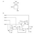
上記特許文献1に記載のブルー相液晶の駆動方式であるIPS(In−Plane Switching)方式では、交流駆動を行うと、駆動電圧が高くなるといった問題がある。駆動電圧を高く設定する必要がある原因について、図23を参照して以下に説明する。
In the IPS (In-Plane Switching) method, which is a blue phase liquid crystal driving method described in
図23(A)は、液晶表示装置が有する画素の回路構成を示している。画素2300は、トランジスタ2301と、液晶素子2302と、保持容量2303とを有する。信号線2304(データ線、ソースライン、又はデータ信号線ともいう)には、画像信号(ビデオ信号ともいう)が入力され、走査線2305(ゲート線、ゲートライン、又はゲート信号線ともいう)には、ゲート信号(走査信号、選択信号ともいう)が入力される。またコモン線2306(共通電位線ともいう)にはコモン電位(共通電位ともいう)が入力され、容量線2307には固定電位が入力される。なお説明のため、液晶素子2302のトランジスタ2301に接続される側の電極を第1の電極(画素電極ともいう)、コモン線2306に接続される側の電極を第2の電極(対向電極ともいう)という。
FIG. 23A illustrates a circuit configuration of a pixel included in the liquid crystal display device. The
また、液晶表示装置では、液晶素子の劣化(焼き付き)を抑制するために、一定期間毎に、液晶素子における第2の電極の電位(コモン電位ともいう)に対して第1の電極に印加される電圧の極性を反転させる交流駆動が行われている。交流駆動として、フレーム反転駆動、ゲートライン反転駆動、ソースライン反転駆動、ドットライン反転駆動等の駆動方式がある。 In addition, in a liquid crystal display device, in order to suppress deterioration (burn-in) of the liquid crystal element, a potential of the second electrode in the liquid crystal element (also referred to as a common potential) is applied to the first electrode at regular intervals. AC driving is performed to reverse the polarity of the voltage. As AC driving, there are driving methods such as frame inversion driving, gate line inversion driving, source line inversion driving, and dot line inversion driving.
例えば、フレーム反転駆動とは、1フレーム期間毎に、液晶素子に印加される電圧の極性を反転させる駆動方法である。なお、1フレーム期間とは、1画面分の画像を表示する期間に相当し、その期間には特に限定はないが、画像をみる人がちらつき(フリッカ)を感じないように少なくとも1/60秒以下とすることが好ましい。 For example, the frame inversion driving is a driving method in which the polarity of the voltage applied to the liquid crystal element is inverted every frame period. Note that one frame period corresponds to a period during which an image for one screen is displayed. There is no particular limitation on the period, but at least 1/60 second so that a person viewing the image does not feel flicker. The following is preferable.
また、ゲートライン反転駆動とは、同一の走査線に接続された画素が有する液晶素子に印加される電圧の極性を、隣接する走査線に接続された画素が有する液晶素子に対し反転させ、さらに各画素に対しフレーム反転を行う駆動方法である。 In addition, the gate line inversion driving is to invert the polarity of the voltage applied to the liquid crystal elements included in the pixels connected to the same scanning line with respect to the liquid crystal elements included in the pixels connected to the adjacent scanning lines, and This is a driving method for performing frame inversion on each pixel.
図23(B)に、反転駆動を行う場合の図23(A)の画素2300の動作を説明するためのタイミングチャートの一例を示す。図23(B)では、反転駆動の反転駆動期間2311及び非反転駆動期間2312の各1フレーム期間における、走査線(GL)、信号線(SL)、コモン線(CL)、第1の電極(PE)、第2の電極(CE)の電位についてのタイミングチャートを示している。
FIG. 23B illustrates an example of a timing chart for describing operation of the
図23(B)では、走査線(GL)の走査信号の電位は、画素を選択する期間、すなわちトランジスタ2301を導通状態(オン状態ともいう)とする期間でVgh、他の期間、すなわちトランジスタ2301を非導通状態(オフ状態ともいう)とする期間でVgl(Vgh>Vgl)としている。また、信号線(SL)の画像信号の電位は表示する画像に応じて変動するが、ここでは非反転駆動するための電位としてVdh、反転駆動するための電位としてVdl(Vdh>Vdl)としている。
In FIG. 23B, the potential of the scan signal of the scan line (GL) is Vgh in a period for selecting a pixel, that is, a period in which the
なお、図23(B)では、信号線(SL)の画像信号の階調に応じて第1の電極(PE)の電位が異なることとなるが、説明のため、走査線(GL)の走査信号に応じて反転する(電位がVdh又はVdlとなる)様子を示している。また、図23(B)では、共通電位線(CL)、すなわち第2の電極(CE)の電位をVc(一定)としている。 Note that in FIG. 23B, the potential of the first electrode (PE) varies depending on the gradation of the image signal of the signal line (SL), but for the sake of explanation, scanning of the scanning line (GL) is performed. The state of inversion according to the signal (potential becomes Vdh or Vdl) is shown. In FIG. 23B, the potential of the common potential line (CL), that is, the second electrode (CE) is Vc (constant).
図23(B)を用いて説明した反転駆動による駆動方法では、画像信号の電位の極性を反転させることによって、液晶素子2302の第1の電極の電位を変化させ、第1の電極と第2の電極との間に印加される電圧の極性を交互に切り替える。よって、信号線(SL)に書き込まれる画像信号に要する電位の幅は、フレーム反転駆動を行わない場合に比べて2倍となる。よって、画像信号の振幅電圧が大きいため、消費電力が大きくなってしまう。
In the driving method by inversion driving described with reference to FIG. 23B, the potential of the first electrode of the
そこで本発明の一態様は、信号線に書き込まれる画像信号の振幅電圧を小さくすることができる液晶表示装置を提供することを目的とする。 An object of one embodiment of the present invention is to provide a liquid crystal display device that can reduce the amplitude voltage of an image signal written to a signal line.
又は、本発明の一態様は、信号線に書き込まれる画像信号の振幅電圧を小さくすることができ、走査線駆動回路の電圧を下げることができる液晶表示装置を提供することを目的とする。 Another object of one embodiment of the present invention is to provide a liquid crystal display device in which the amplitude voltage of an image signal written to a signal line can be reduced and the voltage of a scan line driver circuit can be reduced.
又は、本発明の一態様は、フレーム反転駆動し、信号線に書き込まれる画像信号の振幅電圧を小さくすることができる液晶表示装置及びその駆動方法を提供することを目的とする。 Alternatively, it is an object of one embodiment of the present invention to provide a liquid crystal display device that can perform frame inversion driving and reduce the amplitude voltage of an image signal written to a signal line and a driving method thereof.
又は、本発明の一態様は、フレーム反転駆動し、信号線に書き込まれる画像信号の振幅電圧を小さくすることができ、走査線駆動回路の電圧を下げることができる液晶表示装置及びその駆動方法を提供することを目的とする。 Alternatively, according to one embodiment of the present invention, a liquid crystal display device that can perform frame inversion driving, reduce the amplitude voltage of an image signal written to a signal line, and reduce the voltage of a scan line driver circuit and a driving method thereof. The purpose is to provide.
又は、本発明の一態様は、ゲートライン反転駆動し、信号線に書き込まれる画像信号の振幅電圧を小さくすることができる液晶表示装置及びその駆動方法を提供することを目的とする。 Alternatively, it is an object of one embodiment of the present invention to provide a liquid crystal display device that can be driven by gate line inversion and reduce the amplitude voltage of an image signal written to a signal line, and a driving method thereof.
又は、本発明の一態様は、ゲートライン反転駆動し、信号線に書き込まれる画像信号の振幅電圧を小さくすることができ、走査線駆動回路の電圧を下げることができる液晶表示装置及びその駆動方法を提供することを目的とする。 Alternatively, according to one embodiment of the present invention, a liquid crystal display device and a driving method thereof in which gate line inversion driving can be performed, the amplitude voltage of an image signal written to a signal line can be reduced, and the voltage of a scanning line driver circuit can be reduced. The purpose is to provide.
本発明の一態様は、フレーム反転駆動する液晶表示装置であって、液晶表示装置は、複数の画素と、複数のコモン線と、複数の走査線と、を有し、複数の画素の各々は、液晶素子と、液晶素子の第1の電極に印加する電圧を制御するトランジスタと、を有し、複数の走査線の各々は、複数の画素のうち、行方向に配置された画素が有するトランジスタのゲートに電気的に接続され、複数のコモン線の各々は、複数の画素のうち、行方向に配置された画素が有する液晶素子の第2の電極に電気的に接続されている。そして、第1のフレーム期間において、複数の走査線を順次選択するのに同期して、複数のコモン線に順次第1の電位が供給(保持)され、第1のフレーム期間と隣り合う第2のフレーム期間において、複数の走査線を順次選択するのに同期して、複数のコモン線に順次第2の電位が供給(保持)され、第1の電位と第2の電位とは異なる液晶表示装置である。 One embodiment of the present invention is a liquid crystal display device that performs frame inversion driving, and the liquid crystal display device includes a plurality of pixels, a plurality of common lines, and a plurality of scanning lines, and each of the plurality of pixels includes , A liquid crystal element, and a transistor for controlling a voltage applied to the first electrode of the liquid crystal element, and each of the plurality of scanning lines is a transistor included in a pixel arranged in the row direction among the plurality of pixels. Each of the plurality of common lines is electrically connected to a second electrode of a liquid crystal element included in a pixel arranged in the row direction among the plurality of pixels. Then, in synchronization with the sequential selection of the plurality of scanning lines in the first frame period, the first potential is sequentially supplied (held) to the plurality of common lines, and the second adjacent to the first frame period. In the frame period, the second potential is sequentially supplied (held) to the plurality of common lines in synchronization with the sequential selection of the plurality of scanning lines, and the first potential and the second potential are different from each other. Device.
本発明の一態様において、液晶表示装置は、複数のコモン線が保持する電位を供給するシフトレジスタを有し、シフトレジスタは、リセット用パルス出力回路と、セット用パルス出力回路と、を有する。 In one embodiment of the present invention, a liquid crystal display device includes a shift register that supplies a potential held by a plurality of common lines. The shift register includes a reset pulse output circuit and a set pulse output circuit.
本発明の一態様は、ゲートライン反転駆動する液晶表示装置であって、液晶表示装置は、複数の画素と、複数の第1のコモン線と、複数の第2のコモン線と、複数の走査線と、を有し、複数の画素の各々は、液晶素子と、液晶素子の第1の電極に印加する電圧を制御するトランジスタと、を有し、複数の走査線の各々は、複数の画素のうち、行方向に配置された画素が有するトランジスタのゲートに電気的に接続され、複数の第1のコモン線の各々は、複数の画素のうち、奇数行の行方向に配置された画素が有する液晶素子の第2の電極に電気的に接続され、複数の第2のコモン線の各々は、複数の画素のうち、偶数行の行方向に配置された画素が有する液晶素子の第2の電極に電気的に接続されている。そして、第1のフレーム期間において、複数の走査線を順次選択するのに同期して、複数の第1のコモン線に順次第1の電位が供給(保持)される動作と、複数の第2のコモン線に順次第2の電位が供給(保持)される動作と、が交互に行われ、第1のフレーム期間と隣り合う第2のフレーム期間において、複数の走査線を順次選択するのに同期して、複数の第1のコモン線に順次第2の電位が供給(保持)される動作と、複数の第2のコモン線に順次第1の電位が供給(保持)される動作と、が交互に行われ、第1の電位と第2の電位とは異なる液晶表示装置である。 One embodiment of the present invention is a liquid crystal display device that performs gate line inversion driving, and the liquid crystal display device includes a plurality of pixels, a plurality of first common lines, a plurality of second common lines, and a plurality of scans. Each of the plurality of pixels includes a liquid crystal element and a transistor that controls a voltage applied to the first electrode of the liquid crystal element, and each of the plurality of scanning lines includes a plurality of pixels. Among the plurality of pixels, each of the plurality of first common lines is electrically connected to a gate of a transistor included in a pixel arranged in the row direction. The plurality of second common lines are electrically connected to the second electrode of the liquid crystal element having the second liquid crystal element, and each of the plurality of second common lines is a second liquid crystal element included in the pixels arranged in the row direction of even rows among the plurality of pixels. It is electrically connected to the electrode. In addition, in the first frame period, the first potential is sequentially supplied (held) to the plurality of first common lines in synchronization with the sequential selection of the plurality of scanning lines, and the plurality of second lines. The operation of sequentially supplying (holding) the second potential to the common line is alternately performed to sequentially select a plurality of scanning lines in the second frame period adjacent to the first frame period. In synchronization, an operation in which the second potential is sequentially supplied (held) to the plurality of first common lines, and an operation in which the first potential is sequentially supplied (held) to the plurality of second common lines, Are alternately performed, and the first potential and the second potential are different liquid crystal display devices.
本発明の一態様において、液晶表示装置は、複数の第1のコモン線が保持する電位を供給する第1のシフトレジスタと、複数の第2のコモン線が保持する電位を供給する第2のシフトレジスタと、を有し、第1のシフトレジスタと第2のシフトレジスタの各々は、リセット用パルス出力回路と、セット用パルス出力回路と、を有する。 In one embodiment of the present invention, a liquid crystal display device includes: a first shift register that supplies a potential held by a plurality of first common lines; and a second shift register that supplies a potential held by a plurality of second common lines. Each of the first shift register and the second shift register includes a reset pulse output circuit and a set pulse output circuit.
また、本発明の一態様において、リセット用パルス出力回路は、第1のトランジスタ乃至第9のトランジスタと、第1の入力端子乃至第5の入力端子と、出力端子と、第1の電源線乃至第8の電源線と、を有する。リセット用パルス出力回路において、第1のトランジスタは、第1の端子が第1の電源線と接続され、第2の端子が第5のトランジスタの第1の端子と接続され、ゲートが第4の入力端子と接続され、第2のトランジスタは、第1の端子が第5のトランジスタの第1の端子と接続され、第2の端子が第2の電源線と接続され、ゲートが第4のトランジスタのゲートと接続され、第3のトランジスタは、第1の端子が第2の入力端子と接続され、第2の端子が出力端子と接続され、ゲートが第5のトランジスタの第2の端子と接続され、第4のトランジスタは、第1の端子が出力端子と接続され、第2の端子が第3の電源線と接続され、第5のトランジスタは、ゲートが第4の電源線と接続され、第6のトランジスタは、第1の端子が第5の電源線と接続され、第2の端子が第4のトランジスタのゲートと接続され、ゲートが第3の入力端子と接続され、第7のトランジスタは、第1の端子が第6の電源線と接続され、第2の端子が第4のトランジスタのゲートと接続され、ゲートが第1の入力端子と接続され、第8のトランジスタは、第1の端子が第7の電源線と接続され、第2の端子が第4のトランジスタのゲートと接続され、ゲートが第5の入力端子と接続され、第9のトランジスタは、第1の端子が第4のトランジスタのゲートと接続され、第2の端子が第8の電源線と接続され、ゲートが第4の入力端子と接続されている。
In one embodiment of the present invention, the reset pulse output circuit includes the first to ninth transistors, the first input terminal to the fifth input terminal, the output terminal, the first power supply line to And an eighth power line. In the reset pulse output circuit, the first transistor has a first terminal connected to the first power supply line, a second terminal connected to the first terminal of the fifth transistor, and a gate connected to the fourth transistor. The second transistor is connected to the input terminal, the first terminal is connected to the first terminal of the fifth transistor, the second terminal is connected to the second power supply line, and the gate is the fourth transistor. The third transistor has a first terminal connected to the second input terminal, a second terminal connected to the output terminal, and a gate connected to the second terminal of the fifth transistor. The fourth transistor has a first terminal connected to the output terminal, a second terminal connected to the third power supply line, and a fifth transistor having a gate connected to the fourth power supply line, The sixth transistor has a first terminal connected to a fifth power supply. The second terminal is connected to the gate of the fourth transistor, the gate is connected to the third input terminal, and the seventh transistor has the first terminal connected to the sixth power supply line. , The second terminal is connected to the gate of the fourth transistor, the gate is connected to the first input terminal, the eighth transistor has the first terminal connected to the seventh power supply line, The terminal is connected to the gate of the fourth transistor, the gate is connected to the fifth input terminal, the ninth transistor has the first terminal connected to the gate of the fourth transistor, and the second terminal has the
リセット用パルス出力回路において、第1のトランジスタ乃至第9のトランジスタは、Nチャネル型のトランジスタであってもよい。 In the reset pulse output circuit, the first to ninth transistors may be N-channel transistors.
また、本発明の一態様において、リセット用パルス出力回路は、第1のトランジスタ乃至第8のトランジスタと、第1の入力端子乃至第4の入力端子と、出力端子と、第1の電源線乃至第7の電源線と、を有する。リセット用パルス出力回路において、第1のトランジスタは、第1の端子が第1の電源線と接続され、第2の端子が第5のトランジスタの第1の端子と接続され、ゲートが第4の入力端子と接続され、第2のトランジスタは、第1の端子が第5のトランジスタの第1の端子と接続され、第2の端子が第2の電源線と接続され、ゲートが第4のトランジスタのゲートと接続され、第3のトランジスタは、第1の端子が第2の入力端子と接続され、第2の端子が出力端子と接続され、ゲートが第5のトランジスタの第2の端子と接続され、第4のトランジスタは、第1の端子が出力端子と接続され、第2の端子が第3の電源線と接続され、第5のトランジスタは、ゲートが第4の電源線と接続され、第6のトランジスタは、第1の端子が第5の電源線と接続され、第2の端子が第4のトランジスタのゲートと接続され、ゲートが第3の入力端子と接続され、第7のトランジスタは、第1の端子が第6の電源線と接続され、第2の端子が第4のトランジスタのゲートと接続され、ゲートが第1の入力端子と接続され、第8のトランジスタは、第1の端子が第4のトランジスタのゲートと接続され、第2の端子が第7の電源線と接続され、ゲートが第4の入力端子と接続されている。 In one embodiment of the present invention, the reset pulse output circuit includes the first to eighth transistors, the first input terminal to the fourth input terminal, the output terminal, and the first power supply line to And a seventh power line. In the reset pulse output circuit, the first transistor has a first terminal connected to the first power supply line, a second terminal connected to the first terminal of the fifth transistor, and a gate connected to the fourth transistor. The second transistor is connected to the input terminal, the first terminal is connected to the first terminal of the fifth transistor, the second terminal is connected to the second power supply line, and the gate is the fourth transistor. The third transistor has a first terminal connected to the second input terminal, a second terminal connected to the output terminal, and a gate connected to the second terminal of the fifth transistor. The fourth transistor has a first terminal connected to the output terminal, a second terminal connected to the third power supply line, and a fifth transistor having a gate connected to the fourth power supply line, The sixth transistor has a first terminal connected to a fifth power supply. The second terminal is connected to the gate of the fourth transistor, the gate is connected to the third input terminal, and the seventh transistor has the first terminal connected to the sixth power supply line. , The second terminal is connected to the gate of the fourth transistor, the gate is connected to the first input terminal, the eighth transistor has the first terminal connected to the gate of the fourth transistor, and the second transistor Are connected to the seventh power supply line, and the gate is connected to the fourth input terminal.
リセット用パルス出力回路において、第1のトランジスタ乃至第8のトランジスタは、Nチャネル型のトランジスタであってもよい。 In the reset pulse output circuit, the first to eighth transistors may be N-channel transistors.
また、本発明の一態様において、セット用パルス出力回路は、第1のトランジスタ乃至第10のトランジスタと、第1の容量素子と、第2の容量素子と、第1の入力端子乃至第4の入力端子と、第1の出力端子と、第2の出力端子と、第1の電源線乃至第10の電源線と、を有する。セット用パルス出力回路において、第1のトランジスタは、第1の端子が第1の電源線と接続され、第2の端子が第1の出力端子と接続され、第2のトランジスタは、第1の端子が第1の出力端子と接続され、第2の端子が第2の電源線と接続され、第3のトランジスタは、第1の端子が第2の入力端子と接続され、第2の端子が第2の出力端子と接続され、ゲートが第1のトランジスタのゲートと接続され、第4のトランジスタは、第1の端子が第2の出力端子と接続され、第2の端子が第3の電源線と接続され、ゲートが第2のトランジスタのゲートと接続され、第5のトランジスタは、第1の端子が第6のトランジスタの第1の端子と接続され、第2の端子が第1のトランジスタのゲートと接続され、ゲートが第4の電源線と接続され、第6のトランジスタは、第2の端子が第5の電源線と接続され、ゲートが第2のトランジスタのゲートと接続され、第7のトランジスタは、第1の端子が第6の電源線と接続され、第2の端子が第6のトランジスタの第1の端子と接続され、ゲートが第3の入力端子と接続され、第8のトランジスタは、第1の端子が第7の電源線と接続され、第2の端子が第2のトランジスタのゲートと接続され、ゲートが第1の入力端子と接続され、第9のトランジスタは、第1の端子が第8の電源線と接続され、第2の端子が第2のトランジスタのゲートと接続され、ゲートが第4の入力端子と接続され、第10のトランジスタは、第1の端子が第2のトランジスタのゲートと接続され、第2の端子が第9の電源線と接続され、ゲートが第3の入力端子と接続され、第1の容量素子は、一方の端子が第1のトランジスタのゲートと接続され、他方の端子が第1の出力端子と接続され、第2の容量素子は、一方の端子が第2のトランジスタのゲートと接続され、他方の端子が第10の電源線と接続されている。
In one embodiment of the present invention, the setting pulse output circuit includes the first to tenth transistors, the first capacitor, the second capacitor, and the first input terminal to the fourth transistor. An input terminal; a first output terminal; a second output terminal; and a first power supply line to a tenth power supply line. In the setting pulse output circuit, the first transistor has a first terminal connected to the first power supply line, a second terminal connected to the first output terminal, and the second transistor includes the first transistor The terminal is connected to the first output terminal, the second terminal is connected to the second power supply line, the third transistor has the first terminal connected to the second input terminal, and the second terminal The second output terminal is connected, the gate is connected to the gate of the first transistor, the fourth transistor is connected to the second output terminal, and the second terminal is connected to the third power supply. Connected to the line, the gate is connected to the gate of the second transistor, the fifth transistor has a first terminal connected to the first terminal of the sixth transistor, and a second terminal connected to the first transistor. And the gate is connected to the fourth power line. The sixth transistor has a second terminal connected to the fifth power supply line, a gate connected to the gate of the second transistor, and a seventh transistor connected to the sixth power supply line. The second terminal is connected to the first terminal of the sixth transistor, the gate is connected to the third input terminal, and the eighth transistor has the first terminal connected to the seventh power supply line. , The second terminal is connected to the gate of the second transistor, the gate is connected to the first input terminal, the ninth transistor has the first terminal connected to the eighth power supply line, The terminal is connected to the gate of the second transistor, the gate is connected to the fourth input terminal, the tenth transistor has the first terminal connected to the gate of the second transistor, and the second terminal has the
セット用パルス出力回路において、第1のトランジスタ乃至第10のトランジスタは、Nチャネル型のトランジスタであってもよい。 In the setting pulse output circuit, the first to tenth transistors may be N-channel transistors.
また、本発明の一態様において、液晶素子が有する液晶層に、ブルー相を示す液晶材料を用いてもよい。 In one embodiment of the present invention, a liquid crystal material exhibiting a blue phase may be used for a liquid crystal layer included in the liquid crystal element.
本発明の一態様によれば、信号線に書き込まれる画像信号の振幅電圧を小さくすることができる液晶表示装置を提供することができる。 According to one embodiment of the present invention, a liquid crystal display device that can reduce the amplitude voltage of an image signal written to a signal line can be provided.
又は、本発明の一態様によれば、信号線に書き込まれる画像信号の振幅電圧を小さくすることができ、走査線駆動回路の電圧を下げることができる液晶表示装置を提供することができる。 Alternatively, according to one embodiment of the present invention, a liquid crystal display device that can reduce the amplitude voltage of an image signal written to a signal line and reduce the voltage of a scan line driver circuit can be provided.
又は、本発明の一態様によれば、フレーム反転駆動し、信号線に書き込まれる画像信号の振幅電圧を小さくすることができる液晶表示装置及びその駆動方法を提供することができる。 Alternatively, according to one embodiment of the present invention, it is possible to provide a liquid crystal display device that can perform frame inversion driving and reduce the amplitude voltage of an image signal written to a signal line and a driving method thereof.
又は、本発明の一態様によれば、フレーム反転駆動し、信号線に書き込まれる画像信号の振幅電圧を小さくすることができ、走査線駆動回路の電圧を下げることができる液晶表示装置及びその駆動方法を提供することができる。 Alternatively, according to one embodiment of the present invention, a liquid crystal display device that can perform frame inversion driving, reduce the amplitude voltage of an image signal written to a signal line, and reduce the voltage of a scanning line driver circuit and the driving thereof A method can be provided.
又は、本発明の一態様によれば、ゲートライン反転駆動し、信号線に書き込まれる画像信号の振幅電圧を小さくすることができる液晶表示装置及びその駆動方法を提供することができる。 Alternatively, according to one embodiment of the present invention, it is possible to provide a liquid crystal display device and a driving method thereof in which gate line inversion driving is performed and the amplitude voltage of an image signal written to a signal line can be reduced.
又は、本発明の一態様によれば、ゲートライン反転駆動し、信号線に書き込まれる画像信号の振幅電圧を小さくすることができ、走査線駆動回路の電圧を下げることができる液晶表示装置及びその駆動方法を提供することができる。 Alternatively, according to one embodiment of the present invention, a liquid crystal display device that can drive a gate line inversion, reduce the amplitude voltage of an image signal written to a signal line, and reduce the voltage of a scanning line driver circuit and the same A driving method can be provided.
以下、本発明の実施の形態について図面を参照しながら説明する。但し、本発明は多くの異なる態様で実施することが可能であり、本発明の趣旨及びその範囲から逸脱することなくその形態及び詳細を様々に変更し得ることは当業者であれば容易に理解される。従って実施の形態の記載内容に限定して解釈されるものではない。なお、以下に説明する本発明の構成において、同じ物を指し示す符号は異なる図面間において共通とする。 Hereinafter, embodiments of the present invention will be described with reference to the drawings. However, the present invention can be implemented in many different modes, and those skilled in the art can easily understand that the modes and details can be variously changed without departing from the spirit and scope of the present invention. Is done. Therefore, the present invention is not construed as being limited to the description of the embodiments. Note that in the structures of the present invention described below, the same reference numeral is used in different drawings.
なお、各実施の形態の図面等において示す各構成の、大きさ、層の厚さ、信号波形、又は領域は、明瞭化のために誇張されて表記している場合がある。よって、必ずしもそのスケールに限定されない。 Note that the size, layer thickness, signal waveform, or region of each structure illustrated in drawings and the like in the embodiments is exaggerated for simplicity in some cases. Therefore, it is not necessarily limited to the scale.
なお、本明細書にて用いる第1、第2、第3、乃至第N(Nは自然数)という用語は、構成要素の混同を避けるために付したものであり、数的に限定するものではないことを付記する。 Note that the terms “first”, “second”, “third” to “N” (N is a natural number) used in this specification are given to avoid confusion between components, and are not limited in number. It is added that there is no.
なお、本明細書において、AとBとが接続されている、とは、AとBとが直接接続されているものの他、電気的に接続されているものを含むものとする。ここで、AとBとが電気的に接続されているとは、具体的には、トランジスタをはじめとするスイッチング素子を介してAとBとが接続され、当該スイッチング素子の導通によって、AとBとが概略同電位となる場合や、抵抗素子を介してAとBとが接続され、当該抵抗素子の両端に発生する電位差が、AとBとを含む回路の動作に影響しない程度となっている場合等、回路動作を考えた場合、AとBとの間の部分を同じノードとして捉えて差し支えない状態を表す。 Note that in this specification, A and B are connected to each other, including A and B being directly connected, as well as those being electrically connected. Here, A and B are electrically connected. Specifically, A and B are connected via a switching element such as a transistor, and A and B are connected by conduction of the switching element. When B is approximately the same potential or when A and B are connected via a resistance element, the potential difference generated at both ends of the resistance element does not affect the operation of the circuit including A and B. When the circuit operation is considered, such as the case where the part is located, the part between A and B can be regarded as the same node.
(実施の形態1)
本実施の形態では、コモン線駆動回路に設けられるシフトレジスタに関して、リセット用パルス出力回路と、セット用パルス出力回路と、当該リセット用パルス出力回路及びセット用パルス出力回路を有するシフトレジスタの一例を図1〜図10、図22を参照して説明する。
(Embodiment 1)
In this embodiment, an example of a shift register including a reset pulse output circuit, a set pulse output circuit, the reset pulse output circuit, and a set pulse output circuit with respect to the shift register provided in the common line driver circuit. A description will be given with reference to FIGS.
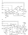
はじめに、本実施の形態で説明する、シフトレジスタが設けられたコモン線駆動回路を有する液晶表示装置の構成について、図22を用いて説明する。 First, a structure of a liquid crystal display device including a common line driver circuit provided with a shift register, which is described in this embodiment, will be described with reference to FIGS.
図22において、液晶表示装置は、基板2207上に、複数の画素2201が、行方向と列方向にマトリクス状に配置(配列)された画素部2202を有し、画素部2202の周辺には、信号線駆動回路2203、走査線駆動回路2204、及びコモン線駆動回路2205を有する。これらの駆動回路には、FPC2206を介して外部より信号が供給される。
22, the liquid crystal display device includes a
なお、信号線駆動回路2203、走査線駆動回路2204、及びコモン線駆動回路2205を、画素部2202と同じ基板上に設ける構成としてもよい。画素部2202と同じ基板上に、信号線駆動回路2203、走査線駆動回路2204、及びコモン線駆動回路2205を設けることで、外部との接続に必要な端子数を削減することができ、液晶表示装置の小型化を図ることができる。
Note that the signal
複数の画素2201のそれぞれは、液晶素子2208、及び液晶素子2208に印加する電圧を制御するトランジスタ2209を有する。なお、画素2201の配置は図22に示す構成に限定されず、縦方向又は横方向において、画素が直線上に並んで配置されている構成や、ギザギザな線上に配置されている構成としてもよい。
Each of the plurality of
本実施の形態において、液晶表示装置を交流駆動させることによって、液晶素子の劣化(焼き付き)を抑制することができる。交流駆動方式として、具体的にはフレーム反転駆動方式又はゲートライン反転駆動方式を用いることができる。 In this embodiment, deterioration (burn-in) of the liquid crystal element can be suppressed by driving the liquid crystal display device with an alternating current. Specifically, a frame inversion driving method or a gate line inversion driving method can be used as the AC driving method.
また、本実施の形態における液晶素子が有する液晶層として、ブルー相を示す液晶材料を用いることができる。ブルー相を示す液晶は、横電界方式で駆動する液晶である。液晶素子のコモン線に接続される側の電極(第2の電極、対向電極ともいう)を、トランジスタに接続される側の電極(第1の電極、画素電極ともいう)と同じ基板に形成して液晶素子を形成する。なお、本実施の形態における液晶素子には、ブルー相を示す液晶に限らず、横電界方式の液晶、または第1の電極及び第2の電極を同じ基板に形成することができる液晶、を用いることができる。 In addition, as the liquid crystal layer included in the liquid crystal element in this embodiment, a liquid crystal material exhibiting a blue phase can be used. A liquid crystal exhibiting a blue phase is a liquid crystal driven by a lateral electric field method. The electrode on the side connected to the common line of the liquid crystal element (also referred to as a second electrode or a counter electrode) is formed over the same substrate as the electrode on the side connected to the transistor (also referred to as a first electrode or a pixel electrode). Thus, a liquid crystal element is formed. Note that a liquid crystal element in this embodiment is not limited to a liquid crystal exhibiting a blue phase, and a horizontal electric field mode liquid crystal or a liquid crystal in which a first electrode and a second electrode can be formed over the same substrate is used. be able to.
コモン線駆動回路2205には、リセット用パルス出力回路及びセット用パルス出力回路を有するシフトレジスタが設けられている。
The common
次に、リセット用パルス出力回路及びセット用パルス出力回路を有するシフトレジスタの構成について、以下に説明する。 Next, the structure of the shift register having the reset pulse output circuit and the set pulse output circuit will be described below.
本実施の形態で示すシフトレジスタの構成について、図1を参照して説明する。シフトレジスタは、第1のリセット用パルス出力回路10_1〜第nのリセット用パルス出力回路10_n(nは2以上の自然数)と、第1のセット用パルス出力回路20_1〜第nのセット用パルス出力回路20_nと、を有している。 A structure of the shift register described in this embodiment is described with reference to FIGS. The shift register includes a first reset pulse output circuit 10_1 to an nth reset pulse output circuit 10_n (n is a natural number of 2 or more) and a first set pulse output circuit 20_1 to an nth set. Pulse output circuit 20_n .
リセット用パルス出力回路について、図2を参照して以下に説明する。 The reset pulse output circuit will be described below with reference to FIG.
第1のリセット用パルス出力回路10_1〜第nのリセット用パルス出力回路10_nの各々は、第1の入力端子201〜第5の入力端子205と、第1の出力端子206と、を有している(図2(A)参照)。
Each of the first reset pulse output circuits 10 - 1 ~ reset pulse output circuit 10 _n n-th, a
第1の入力端子201は、リセット初期化信号線100と接続されている。リセット初期化信号線100にはリセット初期化信号(INI_RES)が入力される。
The
第2の入力端子202及び第3の入力端子203の各々は、第1の信号線101〜第4の信号線104のいずれかと接続されている。例えば、図1において、第1のリセット用パルス出力回路10_1は、第2の入力端子202が第1の信号線101と接続され、第3の入力端子203が第2の信号線102と接続されている。また、第2のリセット用パルス出力回路10_2は、第2の入力端子202が第2の信号線102と接続され、第3の入力端子203が第3の信号線103と接続されている。
Each of the
なお、ここでは、第nのリセット用パルス出力回路10_nの第2の入力端子202と接続されている信号線が第2の信号線102であり、第3の入力端子203と接続されている信号線が第3の信号線103である場合を示しているが、接続されている信号線は、nの値によって異なるものになる。このため、ここで示す構成はあくまでも一例に過ぎないことを付記する。
Note that here, the signal line connected to the
第1の信号線101には第1のリセット用クロック信号(RCLK1)が入力され、第2の信号線102には第2のリセット用クロック信号(RCLK2)が入力され、第3の信号線103には第3のリセット用クロック信号(RCLK3)が入力され、第4の信号線104には第4のリセット用クロック信号(RCLK4)が入力される。
A first reset clock signal (RCLK1) is input to the
リセット用クロック信号(RCLK)は、一定の間隔でH(High)レベルとL(Low)レベルを繰り返す信号である。ここでは、第1のリセット用クロック信号(RCLK1)〜第4のリセット用クロック信号(RCLK4)は、順に1/4周期分遅延している。本実施の形態では、第1のリセット用クロック信号(RCLK1)〜第4のリセット用クロック信号(RCLK4)を利用して、第1のリセット用パルス出力回路10_1〜第nのリセット用パルス出力回路10_nの駆動の制御等を行う。 The reset clock signal (RCLK) is a signal that repeats an H (High) level and an L (Low) level at regular intervals. Here, the first reset clock signal (RCLK1) to the fourth reset clock signal (RCLK4) are sequentially delayed by ¼ period. In the present embodiment, the first reset pulse output circuit 10_1 to the nth reset pulse output are output using the first reset clock signal (RCLK1) to the fourth reset clock signal (RCLK4). Control of driving of the circuit 10_n and the like are performed.
第1のリセット用パルス出力回路10_1の第4の入力端子204は、第1の配線111と接続されている。第1の配線111にはリセットパルス(RSP)が入力される。また、第2のリセット用パルス出力回路10_2〜第nのリセット用パルス出力回路10_nの第4の入力端子204は、一段前段のリセット用パルス出力回路の第1の出力端子206と接続されている。一段前段のリセット用パルス出力回路から、第2のリセット用パルス出力回路10_2〜第nのリセット用パルス出力回路10_nの第4の入力端子204に信号が出力される。
The
第1のリセット用パルス出力回路10_1〜第(n−1)のリセット用パルス出力回路10_n−1の第5の入力端子205は、一段後段のリセット用パルス出力回路の第1の出力端子206と接続されている。一段後段のリセット用パルス出力回路から、第1のリセット用パルス出力回路10_1〜第(n−1)のリセット用パルス出力回路10_n−1の第5の入力端子205に信号が出力される。
The
次に、図1に示す第1のリセット用パルス出力回路10_1〜第nのリセット用パルス出力回路10_nの具体的な構成について、以下に説明する。 Next, specific structures of the first reset pulse output circuit 10_1 to the n-th reset pulse output circuit 10_n illustrated in FIG. 1 are described below.
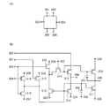
第1のリセット用パルス出力回路10_1〜第nのリセット用パルス出力回路10_nの各々は、トランジスタ221〜トランジスタ229(以下、順に第1のトランジスタ〜第9のトランジスタという。)を有している(図2(B)参照)。また、上述した第1の入力端子201〜第5の入力端子205及び第1の出力端子206に加え、第1の電源線231〜第8の電源線238から、第1のトランジスタ221〜第9のトランジスタ229に信号が入力される。
Each of the first reset pulse output circuits 10 - 1 ~ reset pulse output circuit 10 _n n-th, the
以下において、第1のトランジスタ221〜第9のトランジスタ229をNチャネル型のトランジスタとして説明する。
Hereinafter, the
第1のトランジスタ221は、第1の端子(ソース又はドレインの一方の端子。以下同様。)が第1の電源線231と接続され、第2の端子(ソース又はドレインの他方の端子。以下同様。)が第5のトランジスタ225の第1の端子と接続され、ゲートが第4の入力端子204と接続されている。第2のトランジスタ222は、第1の端子が第5のトランジスタ225の第1の端子と接続され、第2の端子が第2の電源線232と接続され、ゲートが第4のトランジスタ224のゲートと接続されている。
The
第3のトランジスタ223は、第1の端子が第2の入力端子202と接続され、第2の端子が第1の出力端子206と接続され、ゲートが第5のトランジスタ225の第2の端子と接続されている。第4のトランジスタ224は、第1の端子が第1の出力端子206と接続され、第2の端子が第3の電源線233と接続されている。
The
第5のトランジスタ225は、ゲートが第4の電源線234と接続されている。第6のトランジスタ226は、第1の端子が第5の電源線235と接続され、第2の端子が第4のトランジスタ224のゲートと接続され、ゲートが第3の入力端子203と接続されている。
The
第7のトランジスタ227は、第1の端子が第6の電源線236と接続され、第2の端子が第4のトランジスタ224のゲートと接続され、ゲートが第1の入力端子201と接続されている。第8のトランジスタ228は、第1の端子が第7の電源線237と接続され、第2の端子が第4のトランジスタ224のゲートと接続され、ゲートが第5の入力端子205と接続されている。
The
第9のトランジスタ229は、第1の端子が第4のトランジスタ224のゲートと接続され、第2の端子が第8の電源線238と接続され、ゲートが第4の入力端子204と接続されている。
The
なお、第1の電源線231、第4の電源線234〜第7の電源線237には、第1の電位(例えば、VDD)が供給され、第2の電源線232、第3の電源線233、第8の電源線238には、第2の電位(例えば、VSS)が供給されるものとする。ここで、VDD>VSSとする。
Note that a first potential (for example, VDD) is supplied to the first
また、第1のリセット用クロック信号(RCLK1)〜第4のリセット用クロック信号(RCLK4)は、一定の間隔でHレベルとLレベルを繰り返す信号であるが、HレベルのときにVDD、LレベルのときにVSSであるとする。また、ここでは説明の簡略化のためVSS=0とするが、これに限られない。なお、VDDとVSSとの差分は、トランジスタのしきい値電圧よりも大きくなるものとし、すなわちトランジスタを導通状態(オン状態)にするものとする。 Further, the first reset clock signal (RCLK1) to the fourth reset clock signal (RCLK4) are signals that repeat the H level and the L level at regular intervals. Suppose that it is VSS at this time. In addition, here, VSS is set to 0 for simplification of description, but the present invention is not limited to this. Note that the difference between VDD and VSS is larger than the threshold voltage of the transistor, that is, the transistor is turned on (on state).
セット用パルス出力回路について、図3を参照して以下に説明する。 The setting pulse output circuit will be described below with reference to FIG.
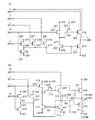
第1のセット用パルス出力回路20_1〜第nのセット用パルス出力回路20_nの各々は、第6の入力端子301〜第9の入力端子304と、第2の出力端子305と、第3の出力端子306と、を有している(図3(A)参照)。
Each of the first set of pulse output circuits 20 - 1 ~ setting pulse output circuit of the n 20 _n includes an
第6の入力端子301は、リセット初期化信号線100と接続されている。リセット初期化信号線100にはリセット初期化信号(INI_RES)が入力される。
The
第7の入力端子302は、第5の信号線105又は第6の信号線106と接続されている。例えば、図1において、第1のセット用パルス出力回路20_1の第7の入力端子302は第5の信号線105と接続されている。また、第2のセット用パルス出力回路20_2の第7の入力端子302は第6の信号線106と接続されている。
The
なお、ここでは、第nのセット用パルス出力回路20_nの第7の入力端子302と接続されている信号線が第6の信号線106である場合を示しているが、接続されている信号線は、nの値によって異なるものになる。このため、ここで示す構成はあくまでも一例に過ぎないことを付記する。
Note that here, the signal line connected to the
第5の信号線105には第1のセット用クロック信号(SCLK1)が入力され、第6の信号線106には第2のセット用クロック信号(SCLK2)が入力される。
The first set clock signal (SCLK1) is input to the
セット用クロック信号(SCLK)は、一定の間隔でH(High)レベルとL(Low)レベルを繰り返す信号である。ここでは、第1のセット用クロック信号(SCLK1)と第2のセット用クロック信号(SCLK2)とは、互いの極性が反転した信号であるとする。本実施の形態では、第1のセット用クロック信号(SCLK1)と第2のセット用クロック信号(SCLK2)を利用して、第1のセット用パルス出力回路20_1〜第nのセット用パルス出力回路20_nの駆動の制御等を行う。 The set clock signal (SCLK) is a signal that repeats the H (High) level and the L (Low) level at regular intervals. Here, it is assumed that the first set clock signal (SCLK1) and the second set clock signal (SCLK2) are signals having opposite polarities. In the present embodiment, the first set pulse output circuit 20_1 to the nth set pulse output are output using the first set clock signal (SCLK1) and the second set clock signal (SCLK2). Control of driving of the circuit 20_n and the like are performed.
第1のセット用パルス出力回路20_1の第8の入力端子303は、第2の配線112と接続されている。第2の配線112にはセットパルス(SSP)が入力される。また、第2のセット用パルス出力回路20_2〜第nのセット用パルス出力回路20_nの第8の入力端子303は、一段前段のセット用パルス出力回路の第3の出力端子306と接続されている。一段前段のセット用パルス出力回路から、第2のセット用パルス出力回路20_2〜第nのセット用パルス出力回路20_nの第8の入力端子303に信号が出力される。
The
第1のセット用パルス出力回路20_1の第9の入力端子304は、第1の配線111と接続されている。また、第2のセット用パルス出力回路20_2〜第nのセット用パルス出力回路20_nの第9の入力端子304は、一段前段のリセット用パルス出力回路の第1の出力端子206と接続されている。一段前段のリセット用パルス出力回路から、第2のセット用パルス出力回路20_2〜第nのセット用パルス出力回路20_nの第9の入力端子304に信号が出力される。
The
第1のセット用パルス出力回路20_1〜第nのセット用パルス出力回路20_nの第2の出力端子305からは、それぞれ、出力信号(OUT(1)〜OUT(n))が出力される。
From the first set of pulse output circuits 20 - 1 ~
次に、第1のセット用パルス出力回路20_1〜第nのセット用パルス出力回路20_nの具体的な構成について、以下に説明する。 Next, specific configurations of the first set pulse output circuit 20_1 to the n-th set pulse output circuit 20_n will be described below.
第1のセット用パルス出力回路20_1〜第nのセット用パルス出力回路20_nの各々は、トランジスタ310〜トランジスタ319(以下、順に第10のトランジスタ〜第19のトランジスタという。)と、容量素子361(以下、第1の容量素子という。)と、容量素子362と(以下、第2の容量素子という。)、を有している(図3(B)参照)。また、上述した第6の入力端子301〜第9の入力端子304、第2の出力端子305、及び第3の出力端子306に加え、第9の電源線329〜第17の電源線337から第10のトランジスタ310〜第19のトランジスタ319に信号が入力される。
Each of the first set of pulse output circuits 20 - 1 ~ setting pulse output circuit 20 _n n-th, the
以下において、第10のトランジスタ310〜第19のトランジスタ319をNチャネル型のトランジスタとして説明する。
Hereinafter, the
第10のトランジスタ310は、第1の端子が第9の電源線329と接続され、第2の端子が第2の出力端子305と接続されている。第11のトランジスタ311は、第1の端子が第2の出力端子305と接続され、第2の端子が第10の電源線330と接続されている。
The
第12のトランジスタ312は、第1の端子が第7の入力端子302と接続され、第2の端子が第3の出力端子306と接続され、ゲートが第10のトランジスタ310のゲートと接続されている。第13のトランジスタ313は、第1の端子が第3の出力端子306と接続され、第2の端子が第11の電源線331と接続され、ゲートが第11のトランジスタ311のゲートと接続されている。
The
第14のトランジスタ314は、第1の端子が第15のトランジスタ315の第1の端子と接続され、第2の端子が第10のトランジスタ310のゲートと接続され、ゲートが第12の電源線332と接続されている。第15のトランジスタ315は、第2の端子が第13の電源線333と接続され、ゲートが第11のトランジスタ311のゲートと接続されている。
The
第16のトランジスタ316は、第1の端子が第14の電源線334と接続され、第2の端子が第15のトランジスタ315の第1の端子と接続され、ゲートが第8の入力端子303と接続されている。第17のトランジスタ317は、第1の端子が第15の電源線335と接続され、第2の端子が第11のトランジスタ311のゲートと接続され、ゲートが第6の入力端子301と接続されている。
The
第18のトランジスタ318は、第1の端子が第16の電源線336と接続され、第2の端子が第11のトランジスタ311のゲートと接続され、ゲートが第9の入力端子304と接続されている。第19のトランジスタ319は、第1の端子が第11のトランジスタ311のゲートと接続され、第2の端子が第17の電源線337と接続され、ゲートが第8の入力端子303と接続されている。
The
第1の容量素子361は、一方の端子が第10のトランジスタ310のゲートと接続され、他方の端子が第2の出力端子305と接続されている。第2の容量素子362は、一方の端子が第11のトランジスタ311のゲートと接続され、他方の端子が第18の電源線338と接続されている。
The
なお、第12の電源線332、第14の電源線334〜第16の電源線336には、第1の電位(例えば、VDD)が供給され、第11の電源線331、第13の電源線333、第17の電源線337、第18の電源線338には、第2の電位(例えば、VSS)が供給されるものとする。
Note that the twelfth
また、第1のセット用クロック信号(SCLK1)及び第2のセット用クロック信号(SCLK2)は、一定の間隔でHレベルとLレベルを繰り返す信号であるが、HレベルのときにVDD、LレベルのときにVSSであるとする。また、ここでは説明の簡略化のためVSS=0とするが、これに限られない。なお、VDDとVSSとの差分は、トランジスタのしきい値電圧よりも大きくなるものとし、すなわちトランジスタを導通状態(オン状態)にするものとする。 The first set clock signal (SCLK1) and the second set clock signal (SCLK2) are signals that repeat H level and L level at regular intervals. Suppose that it is VSS at this time. In addition, here, VSS is set to 0 for simplification of description, but the present invention is not limited to this. Note that the difference between VDD and VSS is larger than the threshold voltage of the transistor, that is, the transistor is turned on (on state).
また、第9の電源線329にはコモン電位(TCOMH)が供給され、第10の電源線330はコモン電位(TCOML)が供給される。ここで、TCOMH>TCOMLとする。コモン線は、コモン電位(TCOMH)又はコモン電位(TCOML)に保持される。
The ninth
次に、図1〜図3で示したシフトレジスタの動作について、図4〜図10を参照して説明する。なお、図4〜図10において、入力端子、出力端子、及び配線の各々から出力される信号の電位がHレベルである場合には「H」、Lレベルである場合には「L」と表記している。 Next, the operation of the shift register shown in FIGS. 1 to 3 will be described with reference to FIGS. 4 to 10, the signal output from each of the input terminal, the output terminal, and the wiring is represented as “H” when the potential of the signal is at the H level, and “L” when the signal is at the L level. doing.
具体的には、図4のタイミングチャートにおいて、第1の期間401〜第6の期間406に分割して説明する。
Specifically, in the timing chart of FIG. 4, the description is divided into a
なお、以下の説明において、第1のトランジスタ221〜第9のトランジスタ229及び第10のトランジスタ310〜第19のトランジスタ319をNチャネル型のトランジスタとし、ゲートとソース間電圧(Vgs)がしきい値電圧(Vth)を上回ったときに導通状態(オン状態)になるものとする。
Note that in the following description, the
第1の期間401において、リセットパルス(RSP)がHレベルになる。
In the
第1の期間401では、第4のリセット用クロック信号(RCLK4)、第1のセット用クロック信号(SCLK1)はHレベル、第1のリセット用クロック信号(RCLK1)〜第3のリセット用クロック信号(RCLK3)、第2のセット用クロック信号(SCLK2)はLレベルである。また、セットパルス(SSP)はLレベルである。
In the
リセットパルス(RSP)がHレベルであるため、第1のリセット用パルス出力回路10_1において、第4の入力端子204にゲートが接続された、第1のトランジスタ221と第9のトランジスタ229が導通状態になる。
Since the reset pulse (RSP) is at the H level, the
このとき、第5のトランジスタ225のゲートには第1の電位(VDD)が印加されているため、第5のトランジスタ225も導通状態になっている。第1のトランジスタ221及び第5のトランジスタ225が導通状態であるため、第3のトランジスタ223は導通状態になる。よって、図5(A)中の点線矢印のように電流が流れ、第1の出力端子206からLレベルの信号が出力される。
At this time, since the first potential (VDD) is applied to the gate of the
また、第1の期間401において、リセットパルス(RSP)がHレベルであるため、第1のセット用パルス出力回路20_1の第9の入力端子304にゲートが接続された第18のトランジスタ318が導通状態になる。
In addition, since the reset pulse (RSP) is at the H level in the
第18のトランジスタ318が導通状態であるため、第11のトランジスタ311、第13のトランジスタ313、第15のトランジスタ315は導通状態になる。第11のトランジスタ311が導通状態であるため、図5(B)中の一点鎖線矢印のように電流が流れ、第2の出力端子305から、出力信号(OUT(1))としてコモン電位(TCOML)が出力される。また、第13のトランジスタ313が導通状態であるため、図5(B)中の点線矢印のように電流が流れ、第3の出力端子306からLレベルの信号が出力される。
Since the
以上のように、第1の期間401において、リセットパルス(RSP)がHレベルであるため、第1のセット用パルス出力回路20_1の第2の出力端子305から、出力信号(OUT(1))としてコモン電位(TCOML)が出力される。
As described above, since the reset pulse (RSP) is at the H level in the
次に、第2の期間402において、リセットパルス(RSP)がLレベルになる。
Next, in the
第2の期間402では、第1のリセット用クロック信号(RCLK1)、第2のセット用クロック信号(SCLK2)はHレベル、第2のリセット用クロック信号(RCLK2)〜第4のリセット用クロック信号(RCLK4)、第1のセット用クロック信号(SCLK1)はLレベルである。また、セットパルス(SSP)はLレベルである。
In the
リセットパルス(RSP)がLレベルであるため、第1のリセット用パルス出力回路10_1において、第4の入力端子204にゲートが接続された、第1のトランジスタ221と第9のトランジスタ229が非導通状態(オフ状態)になる。
Since the reset pulse (RSP) is at the L level, the
このとき、第2のリセット用パルス出力回路10_2の第1の出力端子206から第1のリセット用パルス出力回路10_1の第5の入力端子205に入力される信号がLレベルであるため、第8のトランジスタ228は非導通状態になる。第8のトランジスタ228と第9のトランジスタ229が非導通状態であるため、第2のトランジスタ222、第4のトランジスタ224は非導通状態を保持する。また、第1のトランジスタ221が非導通状態になるため、第3のトランジスタ223は導通状態を保持する。よって、図6(A)中の点線矢印のように電流が流れ、第1の出力端子206からHレベルの信号が出力される。
At this time, the signal input to the second reset
また、第2の期間402において、リセットパルス(RSP)がLレベルであるため、第1のセット用パルス出力回路20_1の第9の入力端子304にゲートが接続された第18のトランジスタ318が非導通状態になる。
Further, since the reset pulse (RSP) is at the L level in the
このとき、第8の入力端子303に入力されるセットパルス(SSP)がLレベルであるため、第16のトランジスタ316及び第19のトランジスタ319も非導通状態である。第18のトランジスタ318及び第19のトランジスタ319が非導通状態なので、第11のトランジスタ311、第13のトランジスタ313、第15のトランジスタ315は、導通状態を保持する。第11のトランジスタ311が導通状態であることによって、図6(B)中の一点鎖線矢印のように電流が流れ、第2の出力端子305からコモン電位(TCOML)が出力される。また、第13のトランジスタ313が導通状態であることにより、図6(B)中の点線矢印のように電流が流れ、第3の出力端子306からLレベルの信号が出力される。
At this time, since the set pulse (SSP) input to the
また、第1のリセット用パルス出力回路10_1の第1の出力端子206から出力される信号がHレベルであるため、第2のリセット用パルス出力回路10_2において、第4の入力端子204から第1のトランジスタ221のゲートと第9のトランジスタ229のゲートに第1の電位(VDD)が印加されて、第1のトランジスタ221と第9のトランジスタ229が導通状態になる。
Further, since the signal output from the
このとき、第5のトランジスタ225のゲートには第1の電位(VDD)が印加されているため、第5のトランジスタ225も導通状態になっている。第1のトランジスタ221及び第5のトランジスタ225が導通状態であるため、第3のトランジスタ223は導通状態になる。よって、図7(A)中の点線矢印のように電流が流れ、第1の出力端子206からLレベルの信号が出力される。
At this time, since the first potential (VDD) is applied to the gate of the
また、第2の期間402において、第1のリセット用パルス出力回路10_1の第1の出力端子206から出力される信号が第1の電位(VDD)であるため、第2のセット用パルス出力回路20_2において、第9の入力端子304にゲートが接続された第18のトランジスタ318が導通状態になる。
In addition, in the
第18のトランジスタ318が導通状態であるため、第11のトランジスタ311、第13のトランジスタ313、第15のトランジスタ315は導通状態になる。第11のトランジスタ311が導通状態であるため、図7(B)中の一点鎖線矢印のように電流が流れ、第2の出力端子305から、出力信号(OUT(2))としてコモン電位(TCOML)が出力される。また、第13のトランジスタ313が導通状態であるため、図7(B)中の点線矢印のように電流が流れ、第3の出力端子306からLレベルの信号が出力される。
Since the
以上のように、第2の期間402において、第2のセット用パルス出力回路20_2の第2の出力端子305から、出力信号(OUT(2))としてコモン電位(TCOML)が出力される。
As described above, in the
また、第3の期間403において、第1の期間401及び第2の期間402で述べたのと同様に、第3のセット用パルス出力回路20_3〜第nのセット用パルス出力回路20_nの第2の出力端子305から、出力信号(OUT(3)〜OUT(n))として、順次コモン電位(TCOML)が出力される。
Further, in the
次に、第4の期間404において、セットパルス(SSP)がHレベルになる。
Next, in the
第4の期間404では、第1のリセット用クロック信号(RCLK1)、第2のセット用クロック信号(SCLK2)はHレベル、第2のリセット用クロック信号(RCLK2)〜第4のリセット用クロック信号(RCLK4)、第1のセット用クロック信号(SCLK1)はLレベルである。また、リセットパルス(RSP)はLレベルである。
In the
よって、第1のトランジスタ221、第2のトランジスタ222、及び第4のトランジスタ224は非導通状態であるため、第3のトランジスタ223の導通状態が保持され、第1の出力端子206から第1の電位(VDD)が出力される(図8(A)参照)。
Accordingly, since the
また、セットパルス(SSP)がHレベルであるため、第1のセット用パルス出力回路20_1において、第8の入力端子303にゲートが接続された、第16のトランジスタ316と第19のトランジスタ319が導通状態になる。
In addition, since the set pulse (SSP) is at the H level, the
このとき、第14のトランジスタ314のゲートには第1の電位(VDD)が印加されているため、第14のトランジスタ314も導通状態になっている。第16のトランジスタ316及び第14のトランジスタ314が導通状態であるため、第10のトランジスタ310及び第12のトランジスタ312は導通状態になる。第10のトランジスタ310が導通状態であるため、図8(B)中の一点鎖線矢印のように電流が流れ、第2の出力端子305から、出力信号(OUT(1))としてコモン電位(TCOMH)が出力される。また、第12のトランジスタ312が導通状態であるため、図8(B)の点線矢印のように電流が流れ、第3の出力端子306からLレベルの信号が出力される。
At this time, since the first potential (VDD) is applied to the gate of the
以上のように、第4の期間404において、セットパルス(SSP)がHレベルであるため、第1のセット用パルス出力回路20_1の第2の出力端子305から、出力信号(OUT(1))としてコモン電位(TCOMH)が出力される。
As described above, since the set pulse (SSP) is at the H level in the
次に、第5の期間405において、セットパルス(SSP)がLレベルになる。
Next, in the
第5の期間405では、第2のリセット用クロック信号(RCLK2)、第1のセット用クロック信号(SCLK1)はHレベル、第1のリセット用クロック信号(RCLK1)、第3のリセット用クロック信号(RCLK3)、第4のリセット用クロック信号(RCLK4)、第2のセット用クロック信号(SCLK2)はLレベルである。また、リセットパルス(RSP)はLレベルである。
In the
第1のリセット用パルス出力回路10_1において、第3の入力端子203に供給される第2のリセット用クロック信号(RCLK2)がHレベルであるため、第6のトランジスタ226は導通状態になる。第6のトランジスタ226が導通状態になるため、第2のトランジスタ222及び第4のトランジスタ224は導通状態になる。第4のトランジスタ224が導通状態であるため、図9(A)中の点線矢印のように電流が流れ、第1の出力端子206からLレベルの信号が出力される。
In the first reset pulse output circuit 10 - 1, a second reset clock signal supplied to the third input terminal 203 (RCLK 2) is because it is H level, the
また、第5の期間405において、セットパルス(SSP)がLレベルであるため、第1のセット用パルス出力回路20_1において、第8の入力端子303にゲートが接続された、第16のトランジスタ316と第19のトランジスタ319が非導通状態になる。よって、第10のトランジスタ310及び第12のトランジスタ312は導通状態に保持される。第10のトランジスタ310が導通状態であることによって、図9(B)の一点鎖線矢印のように電流が流れ、第2の出力端子305から、出力信号(OUT(1))としてコモン電位(TCOMH)が出力される。また、第12のトランジスタ312が導通状態であることによって、図9(B)の点線矢印のように電流が流れ、第3の出力端子306からHレベルの信号が出力される。
In the
また、第1のリセット用パルス出力回路10_1の第1の出力端子206から出力される信号がLレベルであるため、第2のリセット用パルス出力回路10_2において、第4の入力端子204から第1のトランジスタ221のゲートと第9のトランジスタ229のゲートに第2の電位(VSS)が印加されて、第1のトランジスタ221と第9のトランジスタ229が非導通状態になる。
Further, since the signal output from the
よって、第1のトランジスタ221、第2のトランジスタ222、及び第4のトランジスタ224は非導通状態であるため、第3のトランジスタ223の導通状態が保持され、第1の出力端子206から第1の電位(VDD)が出力される(図10(A)参照)。
Accordingly, since the
また、第5の期間405において、第1のセット用パルス出力回路20_1の第3の出力端子306からの出力される信号が第1の電位(VDD)であるため、第2のセット用パルス出力回路20_2において、第8の入力端子303にゲートが接続された第16のトランジスタ316及び第19のトランジスタ319が導通状態になる。また、第14のトランジスタ314のゲートには第1の電位(VDD)が印加されているため、第14のトランジスタ314は導通状態である。第16のトランジスタ316及び第14のトランジスタ314が導通状態であるため、第12のトランジスタ312及び第10のトランジスタ310は導通状態になる。第10のトランジスタ310が導通状態であるため、図10(B)中の一点鎖線矢印のように電流が流れ、第2の出力端子305からコモン電位(TCOMH)が出力される。また、第12のトランジスタ312が導通状態であるため、図10(B)中の点線矢印のように電流が流れ、第3の出力端子306から第2の電位(VSS)が出力される。
In the
以上のように、第5の期間405において、第2のセット用パルス出力回路20_2の第2の出力端子305から、出力信号(OUT(2))としてコモン電位(TCOMH)が出力される。
As described above, in the
また、第6の期間406において、第4の期間404及び第5の期間405で述べたのと同様に、第3のセット用パルス出力回路20_3〜第nのセット用パルス出力回路20_nの第2の出力端子305から、出力信号(OUT(3)〜OUT(n))として、順次コモン電位(TCOMH)が出力される。
Further, in the
そして、コモン線駆動回路において、本実施の形態で説明したシフトレジスタがコモン電位を出力するタイミングと、画素部において、走査線(GL1〜GLn)を選択するタイミングと、を同期させ、且つ、フレーム反転駆動することによって、信号線(SL1〜SLn)に書き込まれる画像信号の振幅電圧を小さくすることができる。 In the common line driver circuit, the timing at which the shift register described in this embodiment outputs a common potential and the timing at which the scan lines (GL 1 to GL n ) are selected in the pixel portion are synchronized, and By performing frame inversion driving, the amplitude voltage of the image signal written to the signal lines (SL 1 to SL n ) can be reduced.
画像信号の振幅電圧を小さくすることができるため、液晶表示装置の消費電力の低減を図ることができる。また、画像信号の振幅電圧を小さくすることができるため、液晶素子を駆動するトランジスタの耐圧のマージンを低く設定できる。 Since the amplitude voltage of the image signal can be reduced, the power consumption of the liquid crystal display device can be reduced. In addition, since the amplitude voltage of the image signal can be reduced, the withstand voltage margin of the transistor that drives the liquid crystal element can be set low.
又は、画像信号の振幅電圧を小さくすることができ、走査線駆動回路の電圧を下げることができるため、液晶表示装置の消費電力の低減を図ることができる。 Alternatively, the amplitude voltage of the image signal can be reduced and the voltage of the scan line driver circuit can be reduced, so that power consumption of the liquid crystal display device can be reduced.
本実施の形態は、他の実施の形態に記載した構成と適宜組み合わせて実施することが可能である。 This embodiment can be implemented in appropriate combination with the structures described in the other embodiments.
(実施の形態2)
本実施の形態では、コモン線駆動回路に設けられるシフトレジスタであって、上記実施の形態1とは異なるシフトレジスタの構成について、以下に説明する。
(Embodiment 2)
In this embodiment, a structure of a shift register provided in the common line driver circuit, which is different from that in
本実施の形態で示すシフトレジスタの構成について、図11を参照して説明する。シフトレジスタは、第1のリセット用パルス出力回路30_1〜第nのリセット用パルス出力回路30_n(nは2以上の自然数)と、第1のセット用パルス出力回路20_1〜第nのセット用パルス出力回路20_nと、を有している。 A structure of the shift register described in this embodiment is described with reference to FIGS. The shift register includes a first reset pulse output circuit 30_1 to an nth reset pulse output circuit 30_n (n is a natural number of 2 or more) and a first set pulse output circuit 20_1 to an nth set. Pulse output circuit 20_n .
リセット用パルス出力回路について、図12を参照して以下に説明する。 The reset pulse output circuit will be described below with reference to FIG.
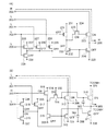
上記実施の形態1では、図1に示すように、第1のリセット用パルス出力回路10_1〜第(n−1)のリセット用パルス出力回路10_n−1(nは2以上の自然数)の第5の入力端子205が、一段後段のリセット用パルス出力回路の第1の出力端子206と接続されている構成を有している。一方、本実施の形態で示すリセット用パルス出力回路では、図11に示すように、第1のリセット用パルス出力回路30_1〜第(n−1)のリセット用パルス出力回路30_n−1(nは2以上の自然数)が第5の入力端子を有していない。
In the first embodiment, as shown in FIG. 1, the first reset pulse output circuit 10_1 to the (n-1) th reset pulse output circuit 10_n-1 (n is a natural number of 2 or more). The
具体的には、第1のリセット用パルス出力回路30_1〜第nのリセット用パルス出力回路30_nの各々は、第1の入力端子1201〜第4の入力端子1204と、第1の出力端子1206と、を有している(図12(A)参照)。
Specifically, each of the first reset pulse output circuits 30 - 1 ~ reset pulse output circuit 30 _n n-th, a
第1の入力端子1201は、リセット初期化信号線100と接続されている。リセット初期化信号線100にはリセット初期化信号(INI_RES)が入力される。
The
第2の入力端子1202及び第3の入力端子1203の各々は、第1の信号線101〜第4の信号線104のいずれかと接続されている。例えば、図11において、第1のリセット用パルス出力回路30_1は、第2の入力端子1202が第1の信号線101と接続され、第3の入力端子1203が第2の信号線102と接続されている。また、第2のリセット用パルス出力回路30_2は、第2の入力端子1202が第2の信号線102と接続され、第3の入力端子1203が第3の信号線103と接続されている。
Each of the
なお、ここでは、第nのリセット用パルス出力回路30_nの第2の入力端子1202と接続されている信号線が第2の信号線102であり、第3の入力端子1203と接続されている信号線が第3の信号線103である場合を示しているが、接続されている信号線は、nの値によって異なるものになる。このため、ここで示す構成はあくまでも一例に過ぎないことを付記する。
Note that here, the signal line connected to the
第1の信号線101には第1のリセット用クロック信号(RCLK1)が入力され、第2の信号線102には第2のリセット用クロック信号(RCLK2)が入力され、第3の信号線103には第3のリセット用クロック信号(RCLK3)が入力され、第4の信号線104には第4のリセット用クロック信号(RCLK4)が入力される。
A first reset clock signal (RCLK1) is input to the
リセット用クロック信号(RCLK)は、一定の間隔でH(High)レベルとL(Low)レベルを繰り返す信号である。ここでは、第1のリセット用クロック信号(RCLK1)〜第4のリセット用クロック信号(RCLK4)は、順に1/4周期分遅延している。本実施の形態では、第1のリセット用クロック信号(RCLK1)〜第4のリセット用クロック信号(RCLK4)を利用して、第1のリセット用パルス出力回路30_1〜第nのリセット用パルス出力回路30_nの駆動の制御等を行う。 The reset clock signal (RCLK) is a signal that repeats an H (High) level and an L (Low) level at regular intervals. Here, the first reset clock signal (RCLK1) to the fourth reset clock signal (RCLK4) are sequentially delayed by ¼ period. In the present embodiment, the first reset pulse output circuit 30_1 to the nth reset pulse output are output using the first reset clock signal (RCLK1) to the fourth reset clock signal (RCLK4). Control of driving of the circuit 30_n and the like are performed.
第1のリセット用パルス出力回路30_1の第4の入力端子1204は、第1の配線111と接続されている。第1の配線111にはリセットパルス(RSP)が入力される。また、第2のリセット用パルス出力回路30_2〜第nのリセット用パルス出力回路30_nの第4の入力端子1204は、一段前段のリセット用パルス出力回路の第1の出力端子1206と接続されている。一段前段のリセット用パルス出力回路から、第2のリセット用パルス出力回路30_2〜第nのリセット用パルス出力回路30_nの第4の入力端子1204に信号が出力される。
A fourth input terminal 1204 of the first reset pulse output circuit 30_1 is connected to the
次に、図11に示す第1のリセット用パルス出力回路30_1〜第nのリセット用パルス出力回路30_nの具体的な構成について、以下に説明する。 Next, specific structures of the first reset pulse output circuit 30_1 to the n-th reset pulse output circuit 30_n illustrated in FIG. 11 are described below.
第1のリセット用パルス出力回路30_1〜第nのリセット用パルス出力回路30_nの各々は、トランジスタ1211〜トランジスタ1218(以下、順に第1のトランジスタ〜第8のトランジスタという。)を有している(図12(B)参照)。また、上述した第1の入力端子1201〜第4の入力端子1204及び第1の出力端子1206に加え、第1の電源線1221〜第7の電源線1227から、第1のトランジスタ1211〜第8のトランジスタ1218に信号が入力される。
Each of the first reset pulse output circuits 30 - 1 ~ reset pulse output circuit 30 _n n-th, the
以下において、第1のトランジスタ1211〜第8のトランジスタ1218をNチャネル型のトランジスタとして説明する。
Hereinafter, the
第1のトランジスタ1211は、第1の端子(ソース又はドレインの一方の端子。以下同様。)が第1の電源線1221と接続され、第2の端子(ソース又はドレインの他方の端子。以下同様。)が第5のトランジスタ1215の第1の端子と接続され、ゲートが第4の入力端子1204と接続されている。第2のトランジスタ1212は、第1の端子が第5のトランジスタ1215の第1の端子と接続され、第2の端子が第2の電源線1222と接続され、ゲートが第4のトランジスタ1214のゲートと接続されている。
In the
第3のトランジスタ1213は、第1の端子が第2の入力端子1202と接続され、第2の端子が第1の出力端子1206と接続され、ゲートが第5のトランジスタ1215の第2の端子と接続されている。第4のトランジスタ1214は、第1の端子が第1の出力端子1206と接続され、第2の端子が第3の電源線1223と接続されている。
The
第5のトランジスタ1215は、ゲートが第4の電源線1224と接続されている。第6のトランジスタ1216は、第1の端子が第5の電源線1225と接続され、第2の端子が第4のトランジスタ1214のゲートと接続され、ゲートが第3の入力端子1203と接続されている。
The
第7のトランジスタ1217は、第1の端子が第6の電源線1226と接続され、第2の端子が第4のトランジスタ1214のゲートと接続され、ゲートが第1の入力端子1201と接続されている。第8のトランジスタ1218は、第1の端子が第4のトランジスタ1214のゲートと接続され、第2の端子が第7の電源線1227と接続され、ゲートが第4の入力端子1204と接続されている。
The
なお、第1の電源線1221、第4の電源線1224、第5の電源線1225、及び第6の電源線1226には、第1の電位(例えば、VDD)が供給され、第2の電源線1222、第3の電源線1223、第7の電源線1227には、第2の電位(例えば、VSS)が供給されるものとする。ここで、VDD>VSSとする。
Note that a first potential (eg, VDD) is supplied to the first
また、第1のリセット用クロック信号(RCLK1)〜第4のリセット用クロック信号(RCLK4)は、一定の間隔でHレベルとLレベルを繰り返す信号であるが、HレベルのときにVDD、LレベルのときにVSSであるとする。また、ここでは説明の簡略化のためVSS=0とするが、これに限られない。なお、VDDとVSSとの差分は、トランジスタのしきい値電圧よりも大きくなるものとし、すなわちトランジスタを導通状態(オン状態)にするものとする。 Further, the first reset clock signal (RCLK1) to the fourth reset clock signal (RCLK4) are signals that repeat the H level and the L level at regular intervals. Suppose that it is VSS at this time. In addition, here, VSS is set to 0 for simplification of description, but the present invention is not limited to this. Note that the difference between VDD and VSS is larger than the threshold voltage of the transistor, that is, the transistor is turned on (on state).
また、第1のセット用パルス出力回路20_1〜第nのセット用パルス出力回路20_nの各々の構成は、実施の形態1で詳述した構成(図3参照)を採用することができるため、ここでは説明を省略する。 In addition, each of the first set pulse output circuit 20_1 to the nth set pulse output circuit 20_n can employ the configuration described in detail in Embodiment 1 (see FIG. 3). The description is omitted here.
また、本実施の形態で説明したシフトレジスタは、実施の形態1で説明した動作(図4〜図10参照)と同様の動作をすることができるため、ここでは説明を省略する。 Further, since the shift register described in this embodiment can perform the same operation as the operation described in Embodiment 1 (see FIGS. 4 to 10), description thereof is omitted here.
コモン線駆動回路において、本実施の形態で説明したシフトレジスタがコモン電位を出力するタイミングと、画素部において、走査線(GL1〜GLn)を選択するタイミングと、を同期させ、且つ、フレーム反転駆動することによって、信号線(SL1〜SLn)に書き込まれる画像信号の振幅電圧を小さくすることができる。 In the common line driver circuit, the timing at which the shift register described in this embodiment outputs a common potential is synchronized with the timing at which the scan lines (GL 1 to GL n ) are selected in the pixel portion, and the frame By performing the inversion driving, the amplitude voltage of the image signal written to the signal lines (SL 1 to SL n ) can be reduced.
画像信号の振幅電圧を小さくすることができるため、液晶表示装置の消費電力の低減を図ることができる。また、画像信号の振幅電圧を小さくすることができるため、液晶素子を駆動するトランジスタの耐圧のマージンを低く設定できる。 Since the amplitude voltage of the image signal can be reduced, the power consumption of the liquid crystal display device can be reduced. In addition, since the amplitude voltage of the image signal can be reduced, the withstand voltage margin of the transistor that drives the liquid crystal element can be set low.
フレーム反転駆動の際、信号線に書き込まれる画像信号の振幅電圧を小さくすることによって、走査線駆動回路の電圧を下げることができるため、液晶表示装置の消費電力の低減を図ることができる。 In the frame inversion driving, the voltage of the scanning line driving circuit can be lowered by reducing the amplitude voltage of the image signal written to the signal line, so that the power consumption of the liquid crystal display device can be reduced.
また、本実施の形態で示すリセット用パルス出力回路を採用することによって、シフトレジスタの配線数を削減できるため、配線の引き回し面積を小さくでき、シフトレジスタのレイアウト面積の縮小を図ることができる。また、配線数を削減できるため、シフトレジスタの歩留まりの向上を図ることができる。 In addition, by employing the reset pulse output circuit described in this embodiment, the number of wirings of the shift register can be reduced, so that the wiring area can be reduced and the layout area of the shift register can be reduced. In addition, since the number of wirings can be reduced, the yield of the shift register can be improved.
本実施の形態は、他の実施の形態に記載した構成と適宜組み合わせて実施することが可能である。 This embodiment can be implemented in appropriate combination with the structures described in the other embodiments.
(実施の形態3)
本実施の形態では、コモン線駆動回路に設けられるシフトレジスタであって、上記実施の形態1〜2とは異なるシフトレジスタの構成について、図13〜図15を参照して説明する。本実施の形態では、コモン線駆動回路に第1のシフトレジスタと第2のシフトレジスタを設ける例を示す。
(Embodiment 3)
In this embodiment, a structure of a shift register provided in the common line driver circuit, which is different from those in
はじめに、第1のリセット用パルス出力回路及び第1のセット用パルス出力回路を有する第1のシフトレジスタの構成について、以下に説明する。 First, the structure of the first shift register including the first reset pulse output circuit and the first set pulse output circuit will be described below.
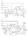
本実施の形態で示す第1のシフトレジスタの構成について、図13を参照して説明する。第1のシフトレジスタは、第1のリセット用パルス出力回路40_1〜第(2m−1)のリセット用パルス出力回路40_2m−1(mは2以上の自然数)と、第1のセット用パルス出力回路50_1〜第(2m−1)のセット用パルス出力回路50_2m−1(mは2以上の自然数)と、を有している。 A structure of the first shift register described in this embodiment is described with reference to FIGS. The first shift register includes a reset pulse output circuit 40 _2M-1 of the first reset pulse output circuits 40 - 1, second (2m-1) (m is a natural number of 2 or more), for a first set pulse setting pulse output circuit 50 _2m-1 of the output circuits 50 - 1, second (2m-1) (m is a natural number of 2 or more) has a, a.
図13で示すリセット用パルス出力回路は、上記実施の形態1又は実施の形態2で説明したリセットパルス出力回路とは、第2の入力端子と第3の入力端子の、第1の信号線101〜第4の信号線104に対する接続がそれぞれ異なっている。
The reset pulse output circuit illustrated in FIG. 13 is different from the reset pulse output circuit described in
具体的には、図13において、第1のリセット用パルス出力回路40_1は、第2の入力端子202が第1の信号線101と接続され、第3の入力端子203が第2の信号線102と接続されている。また、第3のリセット用パルス出力回路40_3は、第2の入力端子202が第3の信号線103と接続され、第3の入力端子203が第4の信号線104と接続されている。
Specifically, in FIG. 13, in the first reset pulse output circuit 40_1 , the
なお、ここでは、第(2m−1)のリセット用パルス出力回路40_2m−1の第2の入力端子202と接続されている信号線が第3の信号線103であり、第3の入力端子203と接続されている信号線が第4の信号線104である場合を示しているが、接続されている信号線は、mの値によって異なるものになる。このため、ここで示す構成はあくまでも一例に過ぎないことを付記する。
Note that here, the signal line connected to the
また、第1のセット用パルス出力回路50_1〜第(2m−1)のセット用パルス出力回路50_2m−1の第2の出力端子305からは、それぞれ、出力信号(OUT(1)〜OUT(2m−1))(mは2以上の自然数)が出力される。
Further, from the first set of pulse output circuits 50 - 1, second (2m-1) setting pulse output circuit 50 _2M-1 of the
なお、第1のシフトレジスタにおける第1の配線1311、第2の配線1312の各々は、図1又は図11の第1の配線111、第2の配線112に対応する。第1の配線1311には第1のリセットパルス(RSP1)が入力され、第2の配線1312には第1のセットパルス(SSP1)が入力される。
Note that each of the
次に、第2のリセット用パルス出力回路及び第2のセット用パルス出力回路を有する第2のシフトレジスタの構成について、以下に説明する。 Next, the structure of the second shift register having the second reset pulse output circuit and the second set pulse output circuit will be described below.
本実施の形態で示す第2のシフトレジスタの構成について、図14を参照して説明する。第2のシフトレジスタは、第2のリセット用パルス出力回路40_2〜第2mのリセット用パルス出力回路40_2m(mは2以上の自然数)と、第2のセット用パルス出力回路50_2〜第2mのセット用パルス出力回路50_2m(mは2以上の自然数)と、を有している。 A structure of the second shift register described in this embodiment is described with reference to FIGS. The second shift register includes a second reset pulse output circuits 40 - 2 ~ a 2m reset pulse output circuit 40 _2m (m is a natural number of 2 or more), - a second set pulse output circuit 50 _2 No. 2 m of setting pulse output circuit 50_2m (m is a natural number of 2 or more).
図14で示すリセット用パルス出力回路は、上記実施の形態1又は実施の形態2で説明したリセットパルス出力回路とは、第2の入力端子と第3の入力端子の、第1の信号線101〜第4の信号線104に対する接続がそれぞれ異なっている。
The reset pulse output circuit illustrated in FIG. 14 is different from the reset pulse output circuit described in
具体的には、図14において、第2のリセット用パルス出力回路40_2は、第2の入力端子202が第2の信号線102と接続され、第3の入力端子203が第3の信号線103と接続されている。また、第4のリセット用パルス出力回路40_4は、第2の入力端子202が第4の信号線104と接続され、第3の入力端子203が第1の信号線101と接続されている。
Specifically, in FIG. 14, in the second reset pulse output circuit 40_2 , the
なお、ここでは、第2mのリセット用パルス出力回路40_2mの第2の入力端子202と接続されている信号線が第4の信号線104であり、第3の入力端子203と接続されている信号線が第1の信号線101である場合を示しているが、接続されている信号線は、mの値によって異なるものになる。このため、ここで示す構成はあくまでも一例に過ぎないことを付記する。
Here, the signal line connected to the
また、第2のセット用パルス出力回路50_2〜第2mのセット用パルス出力回路50_2mの第2の出力端子305からは、それぞれ、出力信号(OUT(2)〜OUT(2m))(mは2以上の自然数)が出力される。
Further, from the
なお、第2のシフトレジスタにおける第1の配線1411、第2の配線1412の各々は、図1又は図11の第1の配線111、第2の配線112に対応する。第1の配線1411には第2のリセットパルス(RSP2)が入力され、第2の配線1412には第2のセットパルス(SSP2)が入力される。
Note that each of the first wiring 1411 and the
なお、第1のシフトレジスタ及び第2のシフトレジスタの各々が有するリセット用パルス出力回路として、例えば、実施の形態1の図2で示したリセット用パルス出力回路や実施の形態2の図12で示したリセット用パルス出力回路を用いることができる。また、第1のシフトレジスタ及び第2のシフトレジスタの各々が有するセット用パルス出力回路として、例えば、実施の形態1の図3で示したセット用パルス出力回路を用いることができる。よってここでは、リセット用パルス出力回路とセット用パルス出力回路の具体的な構成の説明は省略する。
Note that as the reset pulse output circuit included in each of the first shift register and the second shift register, for example, the reset pulse output circuit shown in FIG. 2 of the first embodiment or the reset pulse output circuit shown in FIG. 12 of the second embodiment. The illustrated reset pulse output circuit can be used. As the set pulse output circuit included in each of the first shift register and the second shift register, for example, the set pulse output circuit shown in FIG. 3 of
次に、図13で示した第1シフトレジスタ及び図14で示した第2のシフトレジスタの動作について、図15を参照して説明する。具体的には、図15のタイミングチャートにおいて、第1の期間1501〜第10の期間1510に分割して説明する。
Next, operations of the first shift register shown in FIG. 13 and the second shift register shown in FIG. 14 will be described with reference to FIG. Specifically, in the timing chart of FIG. 15, description is divided into a
なお、以下の説明において、第1のシフトレジスタ及び第2のシフトレジスタが有するトランジスタをNチャネル型のトランジスタとし、ゲートとソース間電圧(Vgs)がしきい値電圧(Vth)を上回ったときに導通状態(オン状態)になるものとする。 Note that in the following description, the transistors included in the first shift register and the second shift register are N-channel transistors, and the gate-source voltage (Vgs) exceeds the threshold voltage (Vth). It shall be a conduction state (ON state).
第1の期間1501では第1のリセットパルス(RSP1)がHレベルになり、第1のシフトレジスタは、実施の形態1の図4で示した第1の期間401と同様に動作する。具体的には、第1のセット用パルス出力回路50_1の第2の出力端子305から、出力信号(OUT(1))としてコモン電位(TCOML)が出力される。
In the
第2の期間1502では第2のセットパルス(SSP2)がHレベルになり、第2のシフトレジスタは、実施の形態1の図4で示した第4の期間404と同様に動作する。具体的には、第2のセット用パルス出力回路50_2の第2の出力端子305から、出力信号(OUT(2))としてコモン電位(TCOMH)が出力される。
In the
第3の期間1503では、第1のシフトレジスタは、実施の形態1の図4で示した第2の期間402と同様に動作する。具体的には、第3のセット用パルス出力回路50_3の第2の出力端子305から、出力信号(OUT(3))としてコモン電位(TCOML)が出力される。
In the
第4の期間1504では、第2のシフトレジスタは、実施の形態1の図4で示した第5の期間405と同様に動作する。具体的には、第4のセット用パルス出力回路50_4の第2の出力端子305から、出力信号(OUT(4))としてコモン電位(TCOMH)が出力される。
In the
第5の期間1505では、第1の期間1501〜第4の期間1504で述べたのと同様に、第5のセット用パルス出力回路50_5〜第(2m−1)のセット用パルス出力回路50_2m−1(mは4以上の自然数)の第2の出力端子305と、第6のセット用パルス出力回路50_6〜第2mのセット用パルス出力回路50_2m(mは4以上の自然数)の第2の出力端子305から、出力信号(OUT(5)〜OUT(2m−1))(mは4以上の自然数)としてコモン電位(TCOML)と、出力信号(OUT(6)〜OUT(2m))(mは4以上の自然数)としてコモン電位(TCOMH)とが、交互に出力される。
In the
第6の期間1506では第2のリセットパルス(RSP2)がHレベルになり、第2のシフトレジスタは、実施の形態1の図4で示した第1の期間401と同様に動作する。具体的には、第2のセット用パルス出力回路50_2の第2の出力端子305から、出力信号(OUT(2))としてコモン電位(TCOML)が出力される。
In the
第7の期間1507では第1のセットパルス(SSP1)がHレベルになり、第1のシフトレジスタは、実施の形態1の図4で示した第4の期間404と同様に動作する。具体的には、第1のセット用パルス出力回路50_1の第2の出力端子305から、出力信号(OUT(1))としてコモン電位(TCOMH)が出力される。
In the
第8の期間1508では、第2のシフトレジスタは、実施の形態1の図4で示した第2の期間402と同様に動作する。具体的には、第4のセット用パルス出力回路50_4の第2の出力端子305から、出力信号(OUT(4))としてコモン電位(TCOML)が出力される。
In the
第9の期間1509では、第1のシフトレジスタは、実施の形態1の図4で示した第5の期間405と同様に動作する。具体的には、第3のセット用パルス出力回路50_3の第2の出力端子305から、出力信号(OUT(3))としてコモン電位(TCOMH)が出力される。
In the
第10の期間1510では、第6の期間1506〜第9の期間1509で述べたのと同様に、第5のセット用パルス出力回路50_5〜第(2m−1)のセット用パルス出力回路502m−1(mは4以上の自然数)_の第2の出力端子305と、第6のセット用パルス出力回路50_6〜第2mのセット用パルス出力回路50_2m(mは4以上の自然数)の第2の出力端子305から、出力信号(OUT(5)〜OUT(2m−1))(mは4以上の自然数)としてコモン電位(TCOMH)と、出力信号(OUT(6)〜、OUT(2m))(mは4以上の自然数)としてコモン電位(TCOML)とが、交互に出力される。
In the
そして、コモン線駆動回路において、本実施の形態で説明したシフトレジスタがコモン電位を出力するタイミングと、画素部において、走査線(GL1〜GLn)を選択するタイミングと、を同期させ、且つ、フレーム反転駆動することによって、信号線(SL1〜SLn)に書き込まれる画像信号の振幅電圧を小さくすることができる。 In the common line driver circuit, the timing at which the shift register described in this embodiment outputs a common potential and the timing at which the scan lines (GL 1 to GL n ) are selected in the pixel portion are synchronized, and By performing frame inversion driving, the amplitude voltage of the image signal written to the signal lines (SL 1 to SL n ) can be reduced.
画像信号の振幅電圧を小さくすることができるため、液晶表示装置の消費電力の低減を図ることができる。また、画像信号の振幅電圧を小さくすることができるため、液晶素子を駆動するトランジスタの耐圧のマージンを低く設定できる。 Since the amplitude voltage of the image signal can be reduced, the power consumption of the liquid crystal display device can be reduced. In addition, since the amplitude voltage of the image signal can be reduced, the withstand voltage margin of the transistor that drives the liquid crystal element can be set low.
又は、ゲートライン反転駆動の際、信号線に書き込まれる画像信号の振幅電圧を小さくすることができ、走査線駆動回路の電圧を下げることができるため、液晶表示装置の消費電力の低減を図ることができる。 Alternatively, when the gate line inversion drive is performed, the amplitude voltage of the image signal written to the signal line can be reduced and the voltage of the scan line driver circuit can be reduced, so that the power consumption of the liquid crystal display device can be reduced. Can do.
本実施の形態は、他の実施の形態に記載した構成と適宜組み合わせて実施することが可能である。 This embodiment can be implemented in appropriate combination with the structures described in the other embodiments.
(実施の形態4)
本実施の形態では、上記実施の形態1の図22で示した液晶表示装置が有する駆動回路の構成について、図16を用いて具体的に説明する。
(Embodiment 4)
In this embodiment, the structure of the driver circuit included in the liquid crystal display device shown in FIG. 22 in
図16(A)に、走査線駆動回路2204の構成を示す。走査線駆動回路2204は、シフトレジスタ1614及びバッファ1615を有する。なお、図16(A)において、複数の走査線(GL)をGL1〜GLy(yは任意の自然数)で表している。
FIG. 16A illustrates the structure of the scan
図16(B)に、コモン線駆動回路2205の構成を示す。コモン線駆動回路2205は、シフトレジスタ1618及びバッファ1619を有する。なお、図16(B)において、複数のコモン線(CL)をCL1〜CLy(yは任意の自然数)で表している。上記実施の形態1〜3で説明したシフトレジスタは、コモン線駆動回路2205のシフトレジスタ1618に適用することができる。
FIG. 16B illustrates a structure of the common
図16(C)に、信号線駆動回路2203の構成を示す。信号線駆動回路2203は、シフトレジスタ1611、第1のラッチ回路1612、第2のラッチ回路1613、及びバッファ1617を有する。なお、図16(C)において、複数の信号線(SL)をSL1〜SLx(xは任意の自然数)で表している。
FIG. 16C illustrates the structure of the signal
上記実施の形態1〜3で説明したシフトレジスタをコモン線駆動回路に適用することによって、アモルファスシリコンを用いたトランジスタでシフトレジスタを設けた場合であっても、コモン線駆動回路を高い周波数で動作させることができる。
By applying the shift register described in
また、酸化物半導体を用いたトランジスタでコモン線駆動回路のシフトレジスタを設けることもできる。酸化物半導体を用いたトランジスタは、オフ電流を低減すると共に、オン電流及び電界効果移動度を高めることができ、またアモルファスシリコンと比べて劣化の度合いを低減することができる。そのため、コモン線駆動回路内の誤動作を低減し、より確度の高い動作を保証するコモン線駆動回路とすることができる。 In addition, a shift register of a common line driver circuit can be provided using a transistor including an oxide semiconductor. A transistor including an oxide semiconductor can reduce off-state current, increase on-state current and field-effect mobility, and can reduce the degree of deterioration as compared to amorphous silicon. For this reason, it is possible to reduce a malfunction in the common line driving circuit and to ensure a more accurate operation.
なお、信号線駆動回路、走査線駆動回路、及びコモン線駆動回路の構成は、図16に示した構成に限定されず、例えば、サンプリング回路やレベルシフタ等を具備していてもよい。また、上記駆動回路以外に、CPUやコントローラ等の回路を基板2207に一体形成してもよい。一体形成することによって、接続する外部回路(IC)の個数が減少し、軽量化、薄型化が図れるため、携帯端末等には特に有効である。
Note that the configurations of the signal line driver circuit, the scan line driver circuit, and the common line driver circuit are not limited to the configurations illustrated in FIG. 16, and may include, for example, a sampling circuit, a level shifter, and the like. In addition to the driving circuit, a circuit such as a CPU or a controller may be integrally formed on the
本実施の形態は、他の実施の形態に記載した構成と適宜組み合わせて実施することが可能である。 This embodiment can be implemented in appropriate combination with the structures described in the other embodiments.
(実施の形態5)
上記実施の形態1の図22に示す液晶表示装置は、交流駆動させることによって、液晶素子の劣化(焼き付き)を抑制することができる。
(Embodiment 5)
The liquid crystal display device shown in FIG. 22 of
本実施の形態では、上記実施の形態1〜3で説明したシフトレジスタを用いて、図22に示す液晶表示装置を交流駆動させる場合の具体的な動作について、図17、図18を用いて説明する。
In this embodiment, specific operation in the case where the liquid crystal display device illustrated in FIG. 22 is AC-driven using the shift register described in
まず、実施の形態1又は実施の形態2で説明したシフトレジスタを用いたフレーム反転駆動について、図17を用いて説明する。
First, frame inversion driving using the shift register described in
図17(A)に、液晶表示装置を構成する画素部の回路図を示す。図17(A)において、複数の画素1701のそれぞれは、液晶素子1708と、液晶素子1708に印加する電圧を制御するトランジスタ1709を有する。また、複数の走査線(GL)をGL1〜GLy(yは任意の自然数)、複数の信号線(SL)をSL1〜SLx(xは任意の自然数)、複数のコモン線(CL)をCL1〜CLy(yは任意の自然数)で表している。コモン線(CL1〜CLy)は、コモン線駆動回路が有するシフトレジスタに接続されている。
FIG. 17A is a circuit diagram of a pixel portion included in the liquid crystal display device. In FIG. 17A, each of the plurality of
図17(B)は、図17(A)に示した回路をフレーム反転駆動する場合のタイミングチャートである。図17(B)において、第1の電極と第2の電極との間に印加される電圧の極性を、「+」又は「−」で表記している。1フレームにおいて、複数の走査線(GL1〜GLy)が順次選択される。 FIG. 17B is a timing chart in the case of performing frame inversion driving on the circuit illustrated in FIG. In FIG. 17B, the polarity of the voltage applied between the first electrode and the second electrode is represented by “+” or “−”. In one frame, a plurality of scanning lines (GL 1 to GL y ) are sequentially selected.
また、図17(C)に示す模式図は、連続するNフレーム目(Nは任意の自然数)と(N+1)フレーム目とで、1フレーム毎に液晶素子1708の第1の電極と第2の電極との間に印加される電圧の極性が交互に切り替わる様子を示している。
In addition, the schematic diagram illustrated in FIG. 17C illustrates the first electrode and the second electrode of the
フレーム反転駆動を行う場合、信号線(SL)に書き込まれる画像信号の電位の極性を、液晶素子1708の第2の電極の電圧を基準として反転させる。フレーム反転駆動することによって、液晶素子の劣化を防ぐことができる。
When frame inversion driving is performed, the polarity of the potential of the image signal written to the signal line (SL) is inverted with reference to the voltage of the second electrode of the
画像信号の電位の極性を反転させることによって、液晶素子1708の第1の電極(画素電極ともいう)の電位を変化させ、第1の電極と第2の電極との間に印加される電圧の極性を交互に切り替える。よって、信号線(SL)に書き込まれる画像信号に要する電位の幅は、フレーム反転駆動を行わない場合に比べて2倍となる。
By reversing the polarity of the potential of the image signal, the potential of the first electrode (also referred to as a pixel electrode) of the
そこで、本実施の形態においては、画像信号の電位の極性の反転と同期して、第2の電極(対向電極、コモン電極ともいう)の電位を変化させる。 Therefore, in this embodiment, the potential of the second electrode (also referred to as a counter electrode or a common electrode) is changed in synchronization with the reversal of the polarity of the potential of the image signal.
具体的には、図17(C)のNフレーム目において、走査線(GL1〜GLy)を選択するタイミングと、図4で説明した第1の期間401〜第3の期間403において、シフトレジスタが出力信号OUT(1)〜OUT(y)としてコモン電位(TCOML)を出力するタイミングとを、同期させる。また、図17(C)の(N+1)フレーム目において、走査線(GL1〜GLy)を選択するタイミングと、図4で説明した第4の期間404〜第6の期間406において、シフトレジスタが出力信号OUT(1)〜OUT(y)としてコモン電位(TCOMH)を出力するタイミングとを、同期させる。
Specifically, in the Nth frame in FIG. 17C, the shift is performed between the timing for selecting the scanning lines (GL 1 to GL y ) and the
上記のように、走査線(GL1〜GLy)を選択するタイミングと、シフトレジスタがコモン電位を出力するタイミングとを同期させることによって、信号線(SL1〜SLx)に書き込まれる画像信号の振幅電圧を小さくすることができる。これにより、液晶表示装置の消費電力の低減を図ることができる。 As described above, the image signal written to the signal lines (SL 1 to SL x ) is synchronized with the timing for selecting the scanning lines (GL 1 to GL y ) and the timing for the shift register to output the common potential. The amplitude voltage can be reduced. Thereby, the power consumption of the liquid crystal display device can be reduced.
次に、実施の形態3で説明したシフトレジスタを用いたゲートライン反転駆動について、図18を用いて説明する。
Next, gate line inversion driving using the shift register described in
図18(A)に、液晶表示装置を構成する画素部の回路図を示す。図18(A)において、複数の画素1801のそれぞれは、液晶素子1808と、液晶素子1808に印加する電圧を制御するトランジスタ1809を有する。また、複数の走査線(GL)をGL1〜GL2y(yは任意の自然数)、複数の信号線(SL)をSL1〜SLx(xは任意の自然数)、複数のコモン線(CL)をCL1〜CL2y(yは任意の自然数)で表している。コモン線(CL1、CL3〜CL2y−1)(yは任意の自然数)は、コモン線駆動回路が有する第1のシフトレジスタに接続され、コモン線(CL2、CL4〜CL2y)(yは任意の自然数)は、コモン線駆動回路が有する第2のシフトレジスタに接続されている。
FIG. 18A is a circuit diagram of a pixel portion included in the liquid crystal display device. In FIG. 18A, each of the plurality of
図18(B)は、図18(A)に示した回路をゲートライン反転駆動する際のタイミングチャートである。図18(B)において、第1の電極と第2の電極との間に印加される電圧の極性を、「+」又は「−」で表記している。1フレームにおいて、走査線(GL1〜GL2y)が順次選択される。 FIG. 18B is a timing chart when the circuit shown in FIG. In FIG. 18B, the polarity of the voltage applied between the first electrode and the second electrode is represented by “+” or “−”. In one frame, the scanning lines (GL 1 to GL 2y ) are sequentially selected.
また、図18(C)に示す模式図は、連続するNフレーム目(Nは任意の自然数)と(N+1)フレーム目とで、行毎に液晶素子1808の第1の電極と第2の電極との間に印加される電圧の極性が交互に切り替わる様子を示している。
18C illustrates a first electrode and a second electrode of the
ゲートライン反転駆動を行う場合、信号線(SL)に書き込まれる画像信号の電位の極性を、液晶素子1808の第2の電極の電圧を基準として、1つの走査線(GL)選択期間毎に反転させる。これにより、隣り合う走査線(GL)に接続されている画素において、互いに逆の極性の画像信号が入力される。ゲートライン反転駆動することによって、液晶素子の劣化を防ぐとともに、ちらつき(フリッカ)を低減することができる。
In the case of performing gate line inversion driving, the polarity of the potential of the image signal written to the signal line (SL) is inverted for each scanning line (GL) selection period with reference to the voltage of the second electrode of the
画像信号の電位の極性を反転させることによって、液晶素子1808の第1の電極(画素電極ともいう)の電位を変化させ、第1の電極と第2の電極との間に印加される電圧の極性を交互に切り替える。よって、信号線(SL)に書き込まれる画像信号に要する電位の幅は、ゲートライン反転駆動を行わない場合に比べて2倍となる。
By reversing the polarity of the potential of the image signal, the potential of the first electrode (also referred to as a pixel electrode) of the
そこで、本実施の形態においては、画像信号の電位の極性の反転と同期して、第2の電極(対向電極、コモン電極ともいう)の電位を変化させる。 Therefore, in this embodiment, the potential of the second electrode (also referred to as a counter electrode or a common electrode) is changed in synchronization with the reversal of the polarity of the potential of the image signal.
具体的には、図18(C)のNフレーム目において、走査線(GL1〜GL2y)を選択するタイミングと、図15で説明した第1の期間1501〜第5の期間1505において、シフトレジスタが出力信号OUT(1)〜OUT(2y)としてコモン電位(TCOML)又はコモン電位(TCOMH)を出力するタイミングとを、同期させる。また、図18(C)の(N+1)フレーム目において、走査線(GL1〜GL2y)を選択するタイミングと、図15で説明した第6の期間1506〜第10の期間1510において、シフトレジスタが出力信号OUT(1)〜OUT(2y)としてコモン電位(TCOMH)又はコモン電位(TCOML)を出力するタイミングとを、同期させる。
Specifically, in the Nth frame in FIG. 18C, the shift is performed between the timing for selecting the scanning lines (GL 1 to GL 2y ) and the
上記のように、走査線(GL1〜GL2y)を選択するタイミングと、シフトレジスタがコモン電位を出力するタイミングとを同期させることによって、信号線(SL1〜SLx)に書き込まれる画像信号の振幅電圧を小さくすることができる。これにより、液晶表示装置の消費電力の低減を図ることができる。 As described above, the image signal written to the signal lines (SL 1 to SL x ) is synchronized with the timing at which the scanning lines (GL 1 to GL 2y ) are selected and the timing at which the shift register outputs the common potential. The amplitude voltage can be reduced. Thereby, the power consumption of the liquid crystal display device can be reduced.
本実施の形態は、他の実施の形態に記載した構成と適宜組み合わせて実施することが可能である。 This embodiment can be implemented in appropriate combination with the structures described in the other embodiments.
(実施の形態6)
本実施の形態では、液晶表示装置が有する表示パネルの画素の構成の一例について、図19を用いて説明する。
(Embodiment 6)
In this embodiment, an example of a structure of a pixel of a display panel included in a liquid crystal display device will be described with reference to FIGS.
図19(A)は表示パネルが有する複数の画素の1つの平面図を示している。図19(B)は図19(A)の一点鎖線A−Bにおける断面図である。 FIG. 19A is a plan view of one of a plurality of pixels included in the display panel. FIG. 19B is a cross-sectional view taken along one-dot chain line AB in FIG.
なお、画素とは、一つの色要素(例えばR(赤)、G(緑)、及びB(青)のいずれか1つ)の明るさを制御できる表示単位に相当するものとする。従って、カラー表示する場合には、カラー画像の最小表示単位は、Rの画素とGの画素とBの画素との三画素から構成されるものとする。ただし、カラー画像を表示するための色要素は、三色に限定されず、三色以上を用いても良いし、RGB以外の色を用いても良い。 Note that a pixel corresponds to a display unit capable of controlling the brightness of one color element (for example, any one of R (red), G (green), and B (blue)). Therefore, in the case of color display, the minimum display unit of a color image is assumed to be composed of three pixels, an R pixel, a G pixel, and a B pixel. However, the color elements for displaying a color image are not limited to three colors, and three or more colors may be used, or colors other than RGB may be used.
図19(A)において、信号線となる配線層(ソース電極層1901a又はドレイン電極層1901bを含む)は、図中上下方向(列方向)に延伸するように配置されている。走査線となる配線層(ゲート電極層1903を含む)は、ソース電極層1901aに概略直交する方向(図中左右方向(行方向))に延伸するように配置されている。容量配線層1904は、ゲート電極層1903に概略平行な方向であって、且つ、ソース電極層1901aに概略直交する方向(図中左右方向(行方向))に延伸するように配置されている。
In FIG. 19A, a wiring layer (including a
図19(A)において、表示パネルの画素には、ゲート電極層1903を有するトランジスタ1905が設けられている。トランジスタ1905上には、絶縁膜1907及び層間膜1909が設けられている。
In FIG. 19A, a
図19に示す表示パネルの画素は、トランジスタ1905に接続される電極層として透明電極層1910を有する。また、コモン線1916に接続される透明電極層1911を有する。透明電極層1910及び透明電極層1911は、互いの櫛歯状の形状が噛み合うように、且つ離間して設けられている。トランジスタ1905上の絶縁膜1907及び層間膜1909には、開口(コンタクトホール)が形成されている。開口(コンタクトホール)において、透明電極層1910とトランジスタ1905とが接続されている。
A pixel of the display panel illustrated in FIG. 19 includes a
図19に示すトランジスタ1905は、ゲート絶縁層1912を介してゲート電極層1903上に配置された半導体層1913を有し、半導体層1913に接してソース電極層1901a及びドレイン電極層1901bを有する。また、容量配線層1904、ゲート絶縁層1912、及びドレイン電極層1901bが積層して、容量素子1915を形成している。
A
また、トランジスタ1905及び液晶層1917を間に挟んで、第1の基板1918と第2の基板1919とが重畳するように配置されている。
In addition, the
なお、図19(B)では、トランジスタ1905としてボトムゲート構造の逆スタガ型トランジスタを用いる例を示したが、本明細書で開示する液晶表示装置に適用できるトランジスタの構造は特に限定されない。例えば、ゲート絶縁層を介してゲート電極層が半導体層の上側に配置されるトップゲート構造のトランジスタ、及び、ゲート絶縁層を介してゲート電極層が半導体層の下側に配置されるボトムゲート構造のスタガ型トランジスタ及びプレーナ型トランジスタ等を用いることができる。
Note that FIG. 19B illustrates an example in which a bottom-gate inverted staggered transistor is used as the
また、トランジスタ1905は、チャネル形成領域を1つ有するシングルゲート構造、2つ有するダブルゲート構造、及び3つ有するトリプルゲート構造のいずれかであっても良い。また、チャネル形成領域の上下にゲート絶縁層を介して配置された2つのゲート電極層を有する、デュアルゲート型でもよい。
The
本実施の形態は、他の実施の形態に記載した構成と適宜組み合わせて実施することが可能である。 This embodiment can be implemented in appropriate combination with the structures described in the other embodiments.
(実施の形態7)
本実施の形態では、本明細書で開示する液晶表示装置に適用できるトランジスタの構成の一例について、図20を用いて説明する。図20は、トランジスタの断面構造を示している。
(Embodiment 7)
In this embodiment, an example of a structure of a transistor that can be applied to the liquid crystal display device disclosed in this specification will be described with reference to FIGS. FIG. 20 illustrates a cross-sectional structure of the transistor.
なお、図20に示すトランジスタは、半導体層として酸化物半導体を用いるものである。酸化物半導体を用いることのメリットは、トランジスタのオン状態において高い電界効果移動度(最大値で5cm2/Vsec以上、好ましくは最大値で10cm2/Vsec〜150cm2/Vsec)と、トランジスタのオフ状態において低い単位チャネル幅あたりのオフ電流(例えば単位チャネル幅あたりのオフ電流が1aA/μm未満、好ましくは10zA/μm未満、且つ、85℃にて100zA/μm未満)と、が得られることである。
Note that the transistor illustrated in FIG. 20 uses an oxide semiconductor as a semiconductor layer. An advantage of using an oxide semiconductor is higher field-effect mobility in the ON state of the
図20(A)に示すトランジスタ2010は、ボトムゲート構造のトランジスタの一つであり、逆スタガ型トランジスタともいう。
A
トランジスタ2010は、絶縁表面を有する基板2000上に、ゲート電極層2001、ゲート絶縁層2002、酸化物半導体層2003、ソース電極層2005a、及びドレイン電極層2005bを含む。また、トランジスタ2010を覆い、酸化物半導体層2003に積層する絶縁層2007が設けられている。絶縁層2007上にはさらに保護絶縁層2009が形成されている。
The
図20(B)に示すトランジスタ2020は、チャネル保護型(チャネルストップ型ともいう)と呼ばれるボトムゲート構造の一つであり、逆スタガ型トランジスタともいう。
A
トランジスタ2020は、絶縁表面を有する基板2000上に、ゲート電極層2001、ゲート絶縁層2002、酸化物半導体層2003、酸化物半導体層2003のチャネル形成領域を覆うチャネル保護層として機能する絶縁層2027、ソース電極層2005a、及びドレイン電極層2005bを含む。また、トランジスタ2020を覆い、保護絶縁層2009が形成されている。
The
図20(C)に示すトランジスタ2030はボトムゲート型のトランジスタであり、絶縁表面を有する基板2000上に、ゲート電極層2001、ゲート絶縁層2002、ソース電極層2005a、ドレイン電極層2005b、及び酸化物半導体層2003を含む。また、トランジスタ2030を覆い、酸化物半導体層2003に接する絶縁層2007が設けられている。絶縁層2007上にはさらに保護絶縁層2009が形成されている。
A
トランジスタ2030においては、ゲート絶縁層2002は基板2000及びゲート電極層2001上に接して設けられ、ゲート絶縁層2002上にソース電極層2005a、ドレイン電極層2005bが接して設けられている。そして、ゲート絶縁層2002、ソース電極層2005a、及びドレイン電極層2005b上に酸化物半導体層2003が設けられている。
In the
図20(D)に示すトランジスタ2040は、トップゲート構造のトランジスタの一つである。トランジスタ2040は、絶縁表面を有する基板2000上に、絶縁層2037、酸化物半導体層2003、ソース電極層2005a、ドレイン電極層2005b、ゲート絶縁層2002、及びゲート電極層2001を含む。ソース電極層2005a、ドレイン電極層2005bにそれぞれ配線層2036a、配線層2036bが接して設けられ接続している。
A
本実施の形態では、上述のとおり、半導体層として酸化物半導体層2003を用いる。酸化物半導体層2003に用いる酸化物半導体としては、四元系金属酸化物であるIn−Sn−Ga−Zn−O系酸化物半導体や、三元系金属酸化物であるIn−Ga−Zn−O系酸化物半導体、In−Sn−Zn−O系酸化物半導体、In−Al−Zn−O系酸化物半導体、Sn−Ga−Zn−O系酸化物半導体、Al−Ga−Zn−O系酸化物半導体、Sn−Al−Zn−O系酸化物半導体や、二元系金属酸化物であるIn−Zn−O系酸化物半導体、Sn−Zn−O系酸化物半導体、Al−Zn−O系酸化物半導体、Zn−Mg−O系酸化物半導体、Sn−Mg−O系酸化物半導体、In−Mg−O系酸化物半導体、In−Ga−O系酸化物半導体や、In−O系酸化物半導体、Sn−O系酸化物半導体、Zn−O系酸化物半導体等を用いることができる。また、上記酸化物半導体はSiO2を含んでいてもよい。ここで、例えば、In−Ga−Zn−O系酸化物半導体とは、インジウム(In)、ガリウム(Ga)、亜鉛(Zn)を有する酸化物膜、という意味であり、その組成比はとくに問わない。また、InとGaとZn以外の元素を含んでいてもよい。
In this embodiment, as described above, the
また、酸化物半導体層2003として、化学式InMO3(ZnO)m(m>0)で表記される薄膜を用いることができる。ここで、Mは、ガリウム(Ga)、アルミニウム(Al)、マンガン(Mn)及びコバルト(Co)から選ばれた、一又は複数の金属元素を示す。例えば、Mとして、ガリウム(Ga)、ガリウム(Ga)及びアルミニウム(Al)、ガリウム(Ga)及びマンガン(Mn)、又はガリウム(Ga)及びコバルト(Co)等がある。
As the
酸化物半導体層2003を用いたトランジスタ2010、2020、2030、2040は、オフ状態における電流値(オフ電流値)を低くすることができる。よって、画素において、画像信号等の電気信号を保持するための容量素子を小さく設計することができる。よって、画素の開口率の向上を図ることができる。また、開口率の向上により、低消費電力化を図ることができる。
The
また、酸化物半導体層2003を用いたトランジスタ2010、2020、2030、2040は、オフ電流を少なくすることができる。よって、画素において、画像信号等の電気信号の保持時間を長くすることができ、書き込み間隔も長く設定できる。よって、1フレーム期間の周期を長くすることができ、静止画像の表示期間でのリフレッシュ動作の頻度を少なくすることができるため、消費電力を抑制する効果をより高くできる。また、上記トランジスタは、同一基板上に駆動回路及び画素部を作り分けて作製することができるため、液晶表示装置の部品点数を削減することができる。
In addition, the
絶縁表面を有する基板2000として使用することができる基板に大きな制限はない。基板2000として、バリウムホウケイ酸ガラスやアルミノホウケイ酸ガラス等のガラス基板を用いることができる。
There is no particular limitation on a substrate that can be used as the
ボトムゲート構造のトランジスタ2010、2020、2030において、下地膜となる絶縁膜を基板とゲート電極層の間に設けてもよい。下地膜は、基板からの不純物元素の拡散を防止する機能を有し、窒化シリコン膜、酸化シリコン膜、窒化酸化シリコン膜、及び酸化窒化シリコン膜から選ばれた、一又は複数の膜による積層構造により形成することができる。
In the
ゲート電極層2001の材料は、モリブデン、チタン、クロム、タンタル、タングステン、アルミニウム、銅、ネオジム、スカンジウム等の金属材料、又はこれらを主成分とする合金材料を用いて、単層で又は積層して形成することができる。
The material of the
ゲート絶縁層2002は、プラズマCVD法又はスパッタリング法等を用いて、酸化シリコン層、窒化シリコン層、酸化窒化シリコン層、窒化酸化シリコン層、酸化アルミニウム層、窒化アルミニウム層、酸化窒化アルミニウム層、窒化酸化アルミニウム層、又は酸化ハフニウム層を、単層で又は積層して形成することができる。例えば、第1のゲート絶縁層としてプラズマCVD法により膜厚50nm以上200nm以下の窒化シリコン層(SiNy(y>0))を形成し、第1のゲート絶縁層上に第2のゲート絶縁層として膜厚5nm以上300nm以下の酸化シリコン層(SiOx(x>0))を積層して、合計膜厚200nmのゲート絶縁層とする。
The
ソース電極層2005a、ドレイン電極層2005bとしては、例えば、アルミニウム(Al)、クロム(Cr)、銅(Cu)、タンタル(Ta)、チタン(Ti)、モリブデン(Mo)、タングステン(W)からから選ばれた元素を含む金属膜、又は上述した元素を成分とする金属窒化物膜(窒化チタン膜、窒化モリブデン膜、窒化タングステン膜)等の導電膜を用いることができる。また、アルミニウム(Al)、銅(Cu)等の金属膜の下側及び上側の一方又は双方に、チタン(Ti)、モリブデン(Mo)、タングステン(W)等の高融点金属膜又はそれらの金属窒化物膜(窒化チタン膜、窒化モリブデン膜、窒化タングステン膜)を積層させた構成としても良い。
Examples of the
ソース電極層2005a、ドレイン電極層2005bに接続する配線層2036a、配線層2036bのような導電膜も、ソース電極層2005a、ドレイン電極層2005bと同様な材料を用いることができる。
The conductive film such as the
また、ソース電極層2005a及びドレイン電極層2005b(これらと同じ層で形成される配線層を含む)となる導電膜は、導電性の金属酸化物で形成しても良い。導電性の金属酸化物としては、酸化インジウム(In2O3)、酸化スズ(SnO2)、酸化亜鉛(ZnO)、酸化インジウム酸化スズ合金(In2O3―SnO2、ITOと略記する)、酸化インジウム酸化亜鉛合金(In2O3―ZnO)、又はこれらの金属酸化物材料に酸化シリコンを含ませたものを用いることができる。
Alternatively, the conductive film to be the
酸化物半導体層の上方に設けられる絶縁層2007、絶縁層2027、下方に設けられる絶縁層2037として、代表的には、酸化シリコン膜、酸化窒化シリコン膜、酸化アルミニウム膜、又は酸化窒化アルミニウム膜等の無機絶縁膜を用いることができる。
As the insulating
また、酸化物半導体層の上方に設けられる保護絶縁層2009として、代表的には、窒化シリコン膜、窒化アルミニウム膜、窒化酸化シリコン膜、窒化酸化アルミニウム膜等の無機絶縁膜を用いることができる。
As the protective insulating
また、トランジスタに起因する表面の凹凸を低減するために、保護絶縁層2009上に平坦化のための絶縁膜を形成してもよい。平坦化のための絶縁膜としては、例えば、ポリイミド、アクリル樹脂、ベンゾシクロブテン系樹脂等の有機材料を用いることができる。また上記有機材料の他に、低誘電率材料(low−k材料)等を用いることができる。なお、これらの材料で形成される絶縁膜を複数積層させることで、平坦化のための絶縁膜を形成してもよい。
Further, an insulating film for planarization may be formed over the protective insulating
このように、本実施の形態を用いて作製した酸化物半導体層を用いたトランジスタは、オフ電流を少なくすることができる。よって、画素において、画像信号等の電気信号の保持時間を長くすることができ、書き込み間隔も長く設定できる。よって、1フレーム期間の周期を長くすることができ、静止画表示期間でのリフレッシュ動作の頻度を少なくすることができるため、消費電力を抑制する効果をより高くできる。また、酸化物半導体層は、レーザ照射等の処理を経ることなく作製でき、大面積基板にトランジスタを形成することができるため、半導体層として用いるのに好適である。 As described above, the transistor including an oxide semiconductor layer manufactured using this embodiment can reduce off-state current. Therefore, in the pixel, the holding time of an electric signal such as an image signal can be increased, and the writing interval can be set longer. Therefore, the cycle of one frame period can be lengthened, and the frequency of the refresh operation in the still image display period can be reduced, so that the effect of suppressing power consumption can be further increased. In addition, the oxide semiconductor layer can be manufactured without being subjected to treatment such as laser irradiation, and a transistor can be formed over a large-area substrate; therefore, the oxide semiconductor layer is suitable for use as a semiconductor layer.
本実施の形態は、他の実施の形態に記載した構成と適宜組み合わせて実施することが可能である。 This embodiment can be implemented in appropriate combination with the structures described in the other embodiments.
(実施の形態8)
本明細書で開示する液晶表示装置は、さまざまな電子機器(遊技機も含む)に適用することができる。電子機器としては、例えば、テレビジョン装置(テレビ、又はテレビジョン受信機ともいう)、コンピュータ用等のモニタ、デジタルカメラやデジタルビデオカメラ等のカメラ、デジタルフォトフレーム、携帯電話機(携帯電話、携帯電話装置ともいう)、携帯型ゲーム機、携帯情報端末、音響再生装置、パチンコ機等の大型ゲーム機などが挙げられる。上記実施の形態で説明した液晶表示装置を具備する電子機器の例について、図21を用いて説明する。
(Embodiment 8)
The liquid crystal display device disclosed in this specification can be applied to a variety of electronic devices (including game machines). Examples of the electronic device include a television device (also referred to as a television or a television receiver), a monitor for a computer, a camera such as a digital camera or a digital video camera, a digital photo frame, a mobile phone (a mobile phone, a mobile phone). Large-sized game machines such as portable game machines, portable information terminals, sound reproduction apparatuses, and pachinko machines. Examples of electronic devices each including the liquid crystal display device described in the above embodiment will be described with reference to FIGS.
図21(A)は、電子書籍の一例を示している。図21(A)に示す電子書籍は、筐体2100及び筐体2101の2つの筐体で構成されている。筐体2100及び筐体2101は、蝶番2104により一体になっており、開閉動作を行うことができる。このような構成により、書籍のような動作を行うことが可能となる。
FIG. 21A illustrates an example of an electronic book. An electronic book illustrated in FIG. 21A includes two housings, a
筐体2100には表示部2102が組み込まれ、筐体2101には表示部2103が組み込まれている。表示部2102及び表示部2103は、続き画面を表示する構成としてもよいし、異なる画面を表示する構成としてもよい。異なる画面を表示する構成とすることで、例えば右側の表示部(図21(A)では表示部2102)に文章を表示し、左側の表示部(図21(A)では表示部2103)に画像を表示することができる。
A
また、図21(A)では、筐体2100に操作部等を備えた例を示している。例えば、筐体2100は、電源入力端子2105、操作キー2106、スピーカ2107等を備えている。操作キー2106により、頁を送ることができる。なお、筐体の表示部と同一面にキーボードやポインティングディバイス等を備える構成としてもよい。また、筐体の裏面や側面に、外部接続用端子(イヤホン端子、USB端子、USBケーブル等の各種ケーブルと接続可能な端子など)、記録媒体挿入部等を備える構成としてもよい。さらに、図21(A)に示す電子書籍は、電子辞書としての機能を持たせた構成としてもよい。
FIG. 21A illustrates an example in which the
図21(B)は、液晶表示装置を用いたデジタルフォトフレームの一例を示している。例えば、図21(B)に示すデジタルフォトフレームは、筐体2111に表示部2112が組み込まれている。表示部2112は、各種画像を表示することが可能であり、例えば、デジタルカメラ等で撮影した画像データを表示させることで、通常の写真立てと同様に機能させることができる。
FIG. 21B illustrates an example of a digital photo frame using a liquid crystal display device. For example, in a digital photo frame illustrated in FIG. 21B, a
なお、図21(B)に示すデジタルフォトフレームは、操作部、外部接続用端子(USB端子、USBケーブル等の各種ケーブルと接続可能な端子など)、記録媒体挿入部等を備える構成とする。これらの構成は、表示部と同一面に組み込まれていてもよいが、側面や裏面に備えるとデザイン性が向上するため好ましい。例えば、デジタルフォトフレームの記録媒体挿入部に、デジタルカメラで撮影した画像データを記憶したメモリを挿入して画像データを取り込み、取り込んだ画像データを表示部2112に表示させることができる。
Note that the digital photo frame illustrated in FIG. 21B includes an operation portion, an external connection terminal (a terminal that can be connected to various cables such as a USB terminal and a USB cable), a recording medium insertion portion, and the like. These configurations may be incorporated on the same surface as the display portion, but it is preferable to provide them on the side surface or the back surface because the design is improved. For example, a memory storing image data captured by a digital camera can be inserted into the recording medium insertion unit of the digital photo frame to capture the image data, and the captured image data can be displayed on the
図21(C)は、液晶表示装置を用いたテレビジョン装置の一例を示している。図21(C)に示すテレビジョン装置は、筐体2121に表示部2122が組み込まれている。表示部2122により、映像を表示することが可能である。また、ここでは、スタンド2123により筐体2121を支持した構成を示している。表示部2122は、上記実施の形態に示した液晶表示装置を適用することができる。
FIG. 21C illustrates an example of a television set using a liquid crystal display device. In the television device illustrated in FIG. 21C, a
図21(C)に示すテレビジョン装置の操作は、筐体2121が備える操作スイッチや、別体のリモコン操作機により行うことができる。リモコン操作機が備える操作キーにより、チャンネルや音量の操作を行うことができ、表示部2122に表示される映像を操作することができる。また、リモコン操作機に、当該リモコン操作機から出力する情報を表示する表示部を設ける構成としてもよい。
The television device illustrated in FIG. 21C can be operated with an operation switch included in the
図21(D)は、液晶表示装置を用いた携帯電話機の一例を示している。図21(D)に示す携帯電話機は、筐体2131に組み込まれた表示部2132の他、操作ボタン2133、操作ボタン2137、外部接続ポート2134、スピーカ2135、及びマイク2136等を備えている。
FIG. 21D illustrates an example of a mobile phone using a liquid crystal display device. A cellular phone shown in FIG. 21D includes a
図21(D)に示す携帯電話機は、表示部2132がタッチパネルになっており、指等の接触により、表示部2132の表示内容を操作することができる。また、電話の発信、或いはメールの作成等は、表示部2132を指等で接触することにより行うことができる。
In the cellular phone shown in FIG. 21D, the
本実施の形態は、他の実施の形態に記載した構成と適宜組み合わせて実施することが可能である。 This embodiment can be implemented in appropriate combination with the structures described in the other embodiments.
10 リセット用パルス出力回路
20 セット用パルス出力回路
30 リセット用パルス出力回路
40 リセット用パルス出力回路
50 セット用パルス出力回路
100 リセット初期化信号線
101 第1の信号線
102 第2の信号線
103 第3の信号線
104 第4の信号線
105 第5の信号線
106 第6の信号線
111 第1の配線
112 第2の配線
201 第1の入力端子
202 第2の入力端子
203 第3の入力端子
204 第4の入力端子
205 第5の入力端子
206 第1の出力端子
221 トランジスタ
222 トランジスタ
223 トランジスタ
224 トランジスタ
225 トランジスタ
226 トランジスタ
227 トランジスタ
228 トランジスタ
229 トランジスタ
231 第1の電源線
232 第2の電源線
233 第3の電源線
234 第4の電源線
235 第5の電源線
236 第6の電源線
237 第7の電源線
238 第8の電源線
301 第6の入力端子
302 第7の入力端子
303 第8の入力端子
304 第9の入力端子
305 第2の出力端子
306 第3の出力端子
310 トランジスタ
311 トランジスタ
312 トランジスタ
313 トランジスタ
314 トランジスタ
315 トランジスタ
316 トランジスタ
317 トランジスタ
318 トランジスタ
319 トランジスタ
329 第9の電源線
330 第10の電源線
331 第11の電源線
332 第12の電源線
333 第13の電源線
334 第14の電源線
335 第15の電源線
336 第16の電源線
337 第17の電源線
338 第18の電源線
361 容量素子
362 容量素子
401 第1の期間
402 第2の期間
403 第3の期間
404 第4の期間
405 第5の期間
406 第6の期間
1201 第1の入力端子
1202 第2の入力端子
1203 第3の入力端子
1204 第4の入力端子
1206 第1の出力端子
1211 トランジスタ
1212 トランジスタ
1213 トランジスタ
1214 トランジスタ
1215 トランジスタ
1216 トランジスタ
1217 トランジスタ
1218 トランジスタ
1221 第1の電源線
1222 第2の電源線
1223 第3の電源線
1224 第4の電源線
1225 第5の電源線
1226 第6の電源線
1227 第7の電源線
1311 第1の配線
1312 第2の配線
1411 第1の配線
1412 第2の配線
1501 第1の期間
1502 第2の期間
1503 第3の期間
1504 第4の期間
1505 第5の期間
1506 第6の期間
1507 第7の期間
1508 第8の期間
1509 第9の期間
1510 第10の期間
1611 シフトレジスタ
1612 第1のラッチ回路
1613 第2のラッチ回路
1614 シフトレジスタ
1615 バッファ
1617 バッファ
1618 シフトレジスタ
1619 バッファ
1701 画素
1708 液晶素子
1709 トランジスタ
1801 画素
1808 液晶素子
1809 トランジスタ
1901a ソース電極層
1901b ドレイン電極層
1903 ゲート電極層
1904 容量配線層
1905 トランジスタ
1907 絶縁膜
1909 層間膜
1910 透明電極層
1911 透明電極層
1912 ゲート絶縁層
1913 半導体層
1915 容量素子
1916 コモン線
1918 第1の基板
1919 第2の基板
2000 基板
2001 ゲート電極層
2002 ゲート絶縁層
2003 酸化物半導体層
2005a ソース電極層
2005b ドレイン電極層
2007 絶縁層
2009 保護絶縁層
2010 トランジスタ
2020 トランジスタ
2027 絶縁層
2030 トランジスタ
2036a 配線層
2036b 配線層
2037 絶縁層
2040 トランジスタ
2100 筐体
2101 筐体
2102 表示部
2103 表示部
2104 蝶番
2105 電源入力端子
2106 操作キー
2107 スピーカ
2111 筐体
2112 表示部
2121 筐体
2122 表示部
2123 スタンド
2131 筐体
2132 表示部
2133 操作ボタン
2134 外部接続ポート
2135 スピーカ
2136 マイク
2137 操作ボタン
2201 画素
2202 画素部
2203 信号線駆動回路
2204 走査線駆動回路
2205 コモン線駆動回路
2206 FPC
2207 基板
2208 液晶素子
2209 トランジスタ
2300 画素
2301 トランジスタ
2302 液晶素子
2303 保持容量
2304 信号線
2305 走査線
2306 コモン線
2307 容量線
2311 反転駆動期間
2312 非反転駆動期間
10 reset pulse output circuit 20 set pulse output circuit 30 reset pulse output circuit 40 reset pulse output circuit 50 set pulse output circuit 100 reset initialization signal line 101 first signal line 102 second signal line 103 second 3rd signal line 104 4th signal line 105 5th signal line 106 6th signal line 111 1st wiring 112 2nd wiring 201 1st input terminal 202 2nd input terminal 203 3rd input terminal 204 fourth input terminal 205 fifth input terminal 206 first output terminal 221 transistor 222 transistor 223 transistor 224 transistor 225 transistor 226 transistor 227 transistor 228 transistor 229 transistor 231 first power supply line 232 second power supply line 233 second 3 power line 234 4th power line 235 5th power line 236 6th power line 237 7th power line 238 8th power line 301 6th input terminal 302 7th input terminal 303 8th input terminal 304 9th Input terminal 305 second output terminal 306 third output terminal 310 transistor 311 transistor 312 transistor 313 transistor 314 transistor 315 transistor 316 transistor 317 transistor 318 transistor 319 transistor 329 ninth power line 330 tenth power line 331 eleventh Power line 332 12th power line 333 13th power line 334 14th power line 335 15th power line 336 16th power line 337 17th power line 338 18th power line 361 Capacitance element 362 Capacitance element 401 1st period 402 2nd period 4 3 3rd period 404 4th period 405 5th period 406 6th period 1201 1st input terminal 1202 2nd input terminal 1203 3rd input terminal 1204 4th input terminal 1206 1st output terminal 1211 transistor 1212 transistor 1213 transistor 1214 transistor 1214 transistor 1215 transistor 1216 transistor 1217 transistor 1218 transistor 1221 first power line 1222 second power line 1223 third power line 1224 fourth power line 1225 fifth power line 1226 sixth power line 1226 Power line 1227 7th power line 1311 1st wiring 1312 2nd wiring 1411 1st wiring 1412 2nd wiring 1501 1st period 1502 2nd period 1503 3rd period 1504 4th period 1505 1st 5 period 1506 1st Period 1507 seventh period 1508 eighth period 1509 ninth period 1510 tenth period 1611 shift register 1612 first latch circuit 1613 second latch circuit 1614 shift register 1615 buffer 1617 buffer 1618 shift register 1619 buffer 1701 Pixel 1708 Liquid crystal element 1709 Transistor 1801 Pixel 1808 Liquid crystal element 1809 Transistor 1901a Source electrode layer 1901b Drain electrode layer 1903 Gate electrode layer 1904 Capacitance wiring layer 1905 Transistor 1907 Insulating film 1909 Interlayer film 1910 Transparent electrode layer 1911 Transparent electrode layer 1912 Gate insulating layer 1913 Semiconductor layer 1915 Capacitor 1916 Common line 1918 First substrate 1919 Second substrate 2000 Substrate 2001 Gate electrode layer 2002 Gate insulating layer 2003 Oxide semiconductor layer 2005a Source electrode layer 2005b Drain electrode layer 2007 Insulating layer 2009 Protective insulating layer 2010 Transistor 2020 Transistor 2027 Insulating layer 2030 Transistor 2036a Wiring layer 2036b Wiring layer 2037 Insulating layer 2040 Transistor 2100 Housing 2101 Housing 2102 Display unit 2103 Display unit 2104 Hinge 2105 Power input terminal 2106 Operation key 2107 Speaker 2111 Case 2112 Display unit 2121 Case 2122 Display unit 2123 Stand 2131 Case 2132 Display unit 2133 Operation button 2134 External connection port 2135 Speaker 2136 Microphone 2137 Operation Button 2201 Pixel 2202 Pixel portion 2203 Signal line driver circuit 2204 Scan line driver circuit 2205 Como Line drive circuit 2206 FPC
2207
Claims (5)
前記液晶表示装置は、
マトリクス状に配置された複数の画素と、
複数のコモン線と、
複数の走査線と、
前記複数のコモン線が保持する電位を供給する機能を有するシフトレジスタと、を有し、
前記複数の画素の各々は、液晶素子と、前記液晶素子の第1の電極に印加する電圧を制御する機能を有するトランジスタと、を有し、
前記複数の走査線の各々は、前記複数の画素のうち、行方向に配置された画素が有するトランジスタのゲートと電気的に接続され、
前記複数のコモン線の各々は、前記複数の画素のうち、行方向に配置された画素が有する液晶素子の第2の電極と電気的に接続され、
前記シフトレジスタは、リセット用パルス出力回路と、セット用パルス出力回路と、を有し、
前記セット用パルス出力回路は、
第1のトランジスタ乃至第10のトランジスタと、
第1の容量素子と、
第2の容量素子と、
第1の入力端子乃至第4の入力端子と、
第1の出力端子と、
第2の出力端子と、
第1の電源線乃至第10の電源線と、を有し、
前記第1のトランジスタは、第1の端子が前記第1の電源線と接続され、第2の端子が前記第1の出力端子と接続され、
前記第2のトランジスタは、第1の端子が前記第1の出力端子と接続され、第2の端子が前記第2の電源線と接続され、
前記第3のトランジスタは、第1の端子が前記第2の入力端子と接続され、第2の端子が前記第2の出力端子と接続され、ゲートが前記第1のトランジスタのゲートと接続され、
前記第4のトランジスタは、第1の端子が前記第2の出力端子と接続され、第2の端子が前記第3の電源線と接続され、ゲートが前記第2のトランジスタのゲートと接続され、
前記第5のトランジスタは、第1の端子が前記第6のトランジスタの第1の端子と接続され、第2の端子が前記第1のトランジスタのゲートと接続され、ゲートが前記第4の電源線と接続され、
前記第6のトランジスタは、第2の端子が前記第5の電源線と接続され、ゲートが前記第2のトランジスタのゲートと接続され、
前記第7のトランジスタは、第1の端子が前記第6の電源線と接続され、第2の端子が前記第6のトランジスタの第1の端子と接続され、ゲートが前記第3の入力端子と接続され、
前記第8のトランジスタは、第1の端子が前記第7の電源線と接続され、第2の端子が前記第2のトランジスタのゲートと接続され、ゲートが前記第1の入力端子と接続され、
前記第9のトランジスタは、第1の端子が前記第8の電源線と接続され、第2の端子が前記第2のトランジスタのゲートと接続され、ゲートが前記第4の入力端子と接続され、
前記第10のトランジスタは、第1の端子が前記第2のトランジスタのゲートと接続され、第2の端子が前記第9の電源線と接続され、ゲートが前記第3の入力端子と接続され、
前記第1の容量素子は、一方の端子が前記第1のトランジスタのゲートと接続され、他方の端子が前記第1の出力端子と接続され、
前記第2の容量素子は、一方の端子が前記第2のトランジスタのゲートと接続され、他方の端子が前記第10の電源線と接続され、
第1のフレーム期間において、前記複数の走査線が順次選択されるのに同期して、前記複数のコモン線に順次第1の電位が保持され、
前記第1のフレーム期間と隣り合う第2のフレーム期間において、前記複数の走査線が順次選択されるのに同期して、前記複数のコモン線に順次第2の電位が保持され、
前記第1の電位と前記第2の電位とは異なることを特徴とする液晶表示装置。 A liquid crystal display device for frame inversion driving,
The liquid crystal display device
A plurality of pixels arranged in a matrix;
Multiple common wires,
A plurality of scan lines;
A shift register having a function of supplying a potential held by the plurality of common lines ,
Each of the plurality of pixels includes a liquid crystal element and a transistor having a function of controlling a voltage applied to the first electrode of the liquid crystal element.
Each of the plurality of scanning lines is electrically connected to a gate of a transistor included in a pixel arranged in a row direction among the plurality of pixels.
Each of the plurality of common lines is electrically connected to a second electrode of a liquid crystal element included in a pixel arranged in a row direction among the plurality of pixels.
The shift register includes a reset pulse output circuit and a set pulse output circuit,
The set pulse output circuit includes:
A first transistor to a tenth transistor;
A first capacitive element;
A second capacitive element;
A first input terminal to a fourth input terminal;
A first output terminal;
A second output terminal;
A first power line to a tenth power line,
The first transistor has a first terminal connected to the first power supply line, a second terminal connected to the first output terminal,
The second transistor has a first terminal connected to the first output terminal, a second terminal connected to the second power supply line,
The third transistor has a first terminal connected to the second input terminal, a second terminal connected to the second output terminal, a gate connected to the gate of the first transistor,
The fourth transistor has a first terminal connected to the second output terminal, a second terminal connected to the third power supply line, a gate connected to the gate of the second transistor,
The fifth transistor has a first terminal connected to the first terminal of the sixth transistor, a second terminal connected to the gate of the first transistor, and a gate connected to the fourth power supply line. Connected with
The sixth transistor has a second terminal connected to the fifth power supply line, a gate connected to the gate of the second transistor,
The seventh transistor has a first terminal connected to the sixth power supply line, a second terminal connected to the first terminal of the sixth transistor, and a gate connected to the third input terminal. Connected,
The eighth transistor has a first terminal connected to the seventh power supply line, a second terminal connected to the gate of the second transistor, and a gate connected to the first input terminal,
The ninth transistor has a first terminal connected to the eighth power supply line, a second terminal connected to the gate of the second transistor, and a gate connected to the fourth input terminal,
The tenth transistor has a first terminal connected to the gate of the second transistor, a second terminal connected to the ninth power supply line, a gate connected to the third input terminal,
The first capacitor element has one terminal connected to the gate of the first transistor and the other terminal connected to the first output terminal.
The second capacitor element has one terminal connected to the gate of the second transistor and the other terminal connected to the tenth power line.
In the first frame period, the first potential is sequentially held in the plurality of common lines in synchronization with the plurality of scanning lines being sequentially selected.
In a second frame period adjacent to the first frame period, a second potential is sequentially held in the plurality of common lines in synchronization with the plurality of scanning lines being sequentially selected,
The liquid crystal display device, wherein the first potential and the second potential are different.
前記液晶表示装置は、
マトリクス状に配置された複数の画素と、
複数の第1のコモン線と、
複数の第2のコモン線と、
複数の走査線と、
前記複数の第1のコモン線が保持する電位を供給する機能を有する第1のシフトレジスタと、
前記複数の第2のコモン線が保持する電位を供給する機能を有する第2のシフトレジスタと、を有し、
前記複数の画素の各々は、液晶素子と、前記液晶素子の第1の電極に印加する電圧を制御する機能を有するトランジスタと、を有し、
前記複数の走査線の各々は、前記複数の画素のうち、行方向に配置された画素が有するトランジスタのゲートと電気的に接続され、
前記複数の第1のコモン線の各々は、前記複数の画素のうち、奇数行の行方向に配置された画素が有する液晶素子の第2の電極と電気的に接続され、
前記複数の第2のコモン線の各々は、前記複数の画素のうち、偶数行の行方向に配置された画素が有する液晶素子の第2の電極と電気的に接続され、
前記第1のシフトレジスタと前記第2のシフトレジスタの各々は、リセット用パルス出力回路と、セット用パルス出力回路と、を有し、
前記セット用パルス出力回路は、
第1のトランジスタ乃至第10のトランジスタと、
第1の容量素子と、
第2の容量素子と、
第1の入力端子乃至第4の入力端子と、
第1の出力端子と、
第2の出力端子と、
第1の電源線乃至第10の電源線と、を有し、
前記第1のトランジスタは、第1の端子が前記第1の電源線と接続され、第2の端子が前記第1の出力端子と接続され、
前記第2のトランジスタは、第1の端子が前記第1の出力端子と接続され、第2の端子が前記第2の電源線と接続され、
前記第3のトランジスタは、第1の端子が前記第2の入力端子と接続され、第2の端子が前記第2の出力端子と接続され、ゲートが前記第1のトランジスタのゲートと接続され、
前記第4のトランジスタは、第1の端子が前記第2の出力端子と接続され、第2の端子が前記第3の電源線と接続され、ゲートが前記第2のトランジスタのゲートと接続され、
前記第5のトランジスタは、第1の端子が前記第6のトランジスタの第1の端子と接続され、第2の端子が前記第1のトランジスタのゲートと接続され、ゲートが前記第4の電源線と接続され、
前記第6のトランジスタは、第2の端子が前記第5の電源線と接続され、ゲートが前記第2のトランジスタのゲートと接続され、
前記第7のトランジスタは、第1の端子が前記第6の電源線と接続され、第2の端子が前記第6のトランジスタの第1の端子と接続され、ゲートが前記第3の入力端子と接続され、
前記第8のトランジスタは、第1の端子が前記第7の電源線と接続され、第2の端子が前記第2のトランジスタのゲートと接続され、ゲートが前記第1の入力端子と接続され、
前記第9のトランジスタは、第1の端子が前記第8の電源線と接続され、第2の端子が前記第2のトランジスタのゲートと接続され、ゲートが前記第4の入力端子と接続され、
前記第10のトランジスタは、第1の端子が前記第2のトランジスタのゲートと接続され、第2の端子が前記第9の電源線と接続され、ゲートが前記第3の入力端子と接続され、
前記第1の容量素子は、一方の端子が前記第1のトランジスタのゲートと接続され、他方の端子が前記第1の出力端子と接続され、
前記第2の容量素子は、一方の端子が前記第2のトランジスタのゲートと接続され、他方の端子が前記第10の電源線と接続され、
第1のフレーム期間において、前記複数の走査線が順次選択されるのに同期して、前記複数の第1のコモン線に順次第1の電位が保持される動作と、前記複数の第2のコモン線に順次第2の電位が保持される動作と、が交互に行われ、
前記第1のフレーム期間と隣り合う第2のフレーム期間において、前記複数の走査線が順次選択されるのに同期して、前記複数の第1のコモン線に順次前記第2の電位が保持される動作と、前記複数の第2のコモン線に順次前記第1の電位が保持される動作と、が交互に行われ、
前記第1の電位と前記第2の電位とは異なることを特徴とする液晶表示装置。 A liquid crystal display device that performs gate line inversion driving,
The liquid crystal display device
A plurality of pixels arranged in a matrix;
A plurality of first common wires;
A plurality of second common lines;
A plurality of scan lines;
A first shift register having a function of supplying a potential held by the plurality of first common lines;
A second shift register having a function of supplying a potential held by the plurality of second common lines,
Each of the plurality of pixels includes a liquid crystal element and a transistor having a function of controlling a voltage applied to the first electrode of the liquid crystal element.
Each of the plurality of scanning lines is electrically connected to a gate of a transistor included in a pixel arranged in a row direction among the plurality of pixels.
Each of the plurality of first common lines is electrically connected to a second electrode of a liquid crystal element included in a pixel arranged in the row direction of an odd row among the plurality of pixels.
Each of the plurality of second common lines is electrically connected to a second electrode of a liquid crystal element included in pixels arranged in the row direction of even rows among the plurality of pixels.
Each of the first shift register and the second shift register includes a reset pulse output circuit and a set pulse output circuit ,
The set pulse output circuit includes:
A first transistor to a tenth transistor;
A first capacitive element;
A second capacitive element;
A first input terminal to a fourth input terminal;
A first output terminal;
A second output terminal;
A first power line to a tenth power line,
The first transistor has a first terminal connected to the first power supply line, a second terminal connected to the first output terminal,
The second transistor has a first terminal connected to the first output terminal, a second terminal connected to the second power supply line,
The third transistor has a first terminal connected to the second input terminal, a second terminal connected to the second output terminal, a gate connected to the gate of the first transistor,
The fourth transistor has a first terminal connected to the second output terminal, a second terminal connected to the third power supply line, a gate connected to the gate of the second transistor,
The fifth transistor has a first terminal connected to the first terminal of the sixth transistor, a second terminal connected to the gate of the first transistor, and a gate connected to the fourth power supply line. Connected with
The sixth transistor has a second terminal connected to the fifth power supply line, a gate connected to the gate of the second transistor,
The seventh transistor has a first terminal connected to the sixth power supply line, a second terminal connected to the first terminal of the sixth transistor, and a gate connected to the third input terminal. Connected,
The eighth transistor has a first terminal connected to the seventh power supply line, a second terminal connected to the gate of the second transistor, and a gate connected to the first input terminal,
The ninth transistor has a first terminal connected to the eighth power supply line, a second terminal connected to the gate of the second transistor, and a gate connected to the fourth input terminal,
The tenth transistor has a first terminal connected to the gate of the second transistor, a second terminal connected to the ninth power supply line, a gate connected to the third input terminal,
The first capacitor element has one terminal connected to the gate of the first transistor and the other terminal connected to the first output terminal.
The second capacitor element has one terminal connected to the gate of the second transistor and the other terminal connected to the tenth power line.
In the first frame period, the first potential is sequentially held in the plurality of first common lines in synchronization with the plurality of scan lines being sequentially selected, and the plurality of second lines The operation of sequentially holding the second potential on the common line is alternately performed,
In a second frame period adjacent to the first frame period, the second potential is sequentially held in the plurality of first common lines in synchronization with the plurality of scanning lines being sequentially selected. And the operation in which the first potential is sequentially held in the plurality of second common lines are alternately performed,
The liquid crystal display device, wherein the first potential and the second potential are different.
前記第1のトランジスタ乃至前記第10のトランジスタは、Nチャネル型のトランジスタであることを特徴とする液晶表示装置。 In claim 1 or 2 ,
The liquid crystal display device, wherein the first to tenth transistors are N-channel transistors.
前記液晶素子が有する液晶層は、ブルー相を示す液晶材料を有することを特徴とする液晶表示装置。 In any one of Claims 1 thru | or 3 ,
The liquid crystal layer of the liquid crystal element includes a liquid crystal material exhibiting a blue phase.
Priority Applications (1)
| Application Number | Priority Date | Filing Date | Title |
|---|---|---|---|
| JP2011104237A JP5766012B2 (en) | 2010-05-21 | 2011-05-09 | Liquid crystal display |
Applications Claiming Priority (3)
| Application Number | Priority Date | Filing Date | Title |
|---|---|---|---|
| JP2010117010 | 2010-05-21 | ||
| JP2010117010 | 2010-05-21 | ||
| JP2011104237A JP5766012B2 (en) | 2010-05-21 | 2011-05-09 | Liquid crystal display |
Publications (3)
| Publication Number | Publication Date |
|---|---|
| JP2012008535A JP2012008535A (en) | 2012-01-12 |
| JP2012008535A5 JP2012008535A5 (en) | 2014-06-19 |
| JP5766012B2 true JP5766012B2 (en) | 2015-08-19 |
Family
ID=44972139
Family Applications (1)
| Application Number | Title | Priority Date | Filing Date |
|---|---|---|---|
| JP2011104237A Expired - Fee Related JP5766012B2 (en) | 2010-05-21 | 2011-05-09 | Liquid crystal display |
Country Status (2)
| Country | Link |
|---|---|
| US (1) | US8928645B2 (en) |
| JP (1) | JP5766012B2 (en) |
Families Citing this family (12)
| Publication number | Priority date | Publication date | Assignee | Title |
|---|---|---|---|---|
| KR101389120B1 (en) * | 2010-03-02 | 2014-04-25 | 가부시키가이샤 한도오따이 에네루기 켄큐쇼 | Pulse signal output circuit and shift register |
| KR101828960B1 (en) | 2010-03-02 | 2018-02-13 | 가부시키가이샤 한도오따이 에네루기 켄큐쇼 | Pulse signal output circuit and shift register |
| WO2011108345A1 (en) * | 2010-03-02 | 2011-09-09 | Semiconductor Energy Laboratory Co., Ltd. | Pulse signal output circuit and shift register |
| US8718224B2 (en) | 2011-08-05 | 2014-05-06 | Semiconductor Energy Laboratory Co., Ltd. | Pulse signal output circuit and shift register |
| JP2013093565A (en) * | 2011-10-07 | 2013-05-16 | Semiconductor Energy Lab Co Ltd | Semiconductor device |
| US9285848B2 (en) * | 2012-04-27 | 2016-03-15 | Semiconductor Energy Laboratory Co., Ltd. | Power reception control device, power reception device, power transmission and reception system, and electronic device |
| US9041453B2 (en) * | 2013-04-04 | 2015-05-26 | Semiconductor Energy Laboratory Co., Ltd. | Pulse generation circuit and semiconductor device |
| US9459445B1 (en) * | 2014-03-31 | 2016-10-04 | Amazon Technologies, Inc. | Dual gate pixel reset for a display device |
| US9728153B2 (en) * | 2014-10-21 | 2017-08-08 | Omnivision Technologies, Inc. | Display system and method using set/reset pixels |
| CN107871468B (en) * | 2016-09-28 | 2023-09-26 | 合肥鑫晟光电科技有限公司 | Output reset circuit, grid integrated driving circuit, driving method and display device |
| CN110262147B (en) * | 2018-08-10 | 2021-10-29 | 友达光电股份有限公司 | Semiconductor substrate and driving method |
| KR102528519B1 (en) * | 2018-08-23 | 2023-05-03 | 삼성디스플레이 주식회사 | Display device |
Family Cites Families (124)
| Publication number | Priority date | Publication date | Assignee | Title |
|---|---|---|---|---|
| JPS60198861A (en) | 1984-03-23 | 1985-10-08 | Fujitsu Ltd | Thin film transistor |
| JPH0244256B2 (en) | 1987-01-28 | 1990-10-03 | Kagaku Gijutsucho Mukizaishitsu Kenkyushocho | INGAZN2O5DESHIMESARERUROTSUHOSHOKEINOSOJOKOZOOJUSURUKAGOBUTSUOYOBISONOSEIZOHO |
| JPH0244258B2 (en) | 1987-02-24 | 1990-10-03 | Kagaku Gijutsucho Mukizaishitsu Kenkyushocho | INGAZN3O6DESHIMESARERUROTSUHOSHOKEINOSOJOKOZOOJUSURUKAGOBUTSUOYOBISONOSEIZOHO |
| JPS63210023A (en) | 1987-02-24 | 1988-08-31 | Natl Inst For Res In Inorg Mater | Compound having laminar structure of hexagonal crystal system expressed by ingazn4o7 and its production |
| JPH0244260B2 (en) | 1987-02-24 | 1990-10-03 | Kagaku Gijutsucho Mukizaishitsu Kenkyushocho | INGAZN5O8DESHIMESARERUROTSUHOSHOKEINOSOJOKOZOOJUSURUKAGOBUTSUOYOBISONOSEIZOHO |
| JPH0244262B2 (en) | 1987-02-27 | 1990-10-03 | Kagaku Gijutsucho Mukizaishitsu Kenkyushocho | INGAZN6O9DESHIMESARERUROTSUHOSHOKEINOSOJOKOZOOJUSURUKAGOBUTSUOYOBISONOSEIZOHO |
| JPH0244263B2 (en) | 1987-04-22 | 1990-10-03 | Kagaku Gijutsucho Mukizaishitsu Kenkyushocho | INGAZN7O10DESHIMESARERUROTSUHOSHOKEINOSOJOKOZOOJUSURUKAGOBUTSUOYOBISONOSEIZOHO |
| JP3069930B2 (en) * | 1992-02-28 | 2000-07-24 | キヤノン株式会社 | Liquid crystal display |
| JPH05251705A (en) | 1992-03-04 | 1993-09-28 | Fuji Xerox Co Ltd | Thin-film transistor |
| CN1095090C (en) | 1994-05-31 | 2002-11-27 | 株式会社半导体能源研究所 | Electro-optical device |
| JP3479375B2 (en) | 1995-03-27 | 2003-12-15 | 科学技術振興事業団 | Metal oxide semiconductor device in which a pn junction is formed with a thin film transistor made of a metal oxide semiconductor such as cuprous oxide, and methods for manufacturing the same |
| EP0820644B1 (en) | 1995-08-03 | 2005-08-24 | Koninklijke Philips Electronics N.V. | Semiconductor device provided with transparent switching element |
| US5959599A (en) | 1995-11-07 | 1999-09-28 | Semiconductor Energy Laboratory Co., Ltd. | Active matrix type liquid-crystal display unit and method of driving the same |
| JP3625598B2 (en) | 1995-12-30 | 2005-03-02 | 三星電子株式会社 | Manufacturing method of liquid crystal display device |
| US6911962B1 (en) | 1996-03-26 | 2005-06-28 | Semiconductor Energy Laboratory Co., Ltd. | Driving method of active matrix display device |
| US5847687A (en) | 1996-03-26 | 1998-12-08 | Semiconductor Energy Laboratory Co., Ltd. | Driving method of active matrix display device |
| JP4170454B2 (en) | 1998-07-24 | 2008-10-22 | Hoya株式会社 | Article having transparent conductive oxide thin film and method for producing the same |
| JP2000150861A (en) | 1998-11-16 | 2000-05-30 | Tdk Corp | Oxide thin film |
| JP3276930B2 (en) | 1998-11-17 | 2002-04-22 | 科学技術振興事業団 | Transistor and semiconductor device |
| TW460731B (en) | 1999-09-03 | 2001-10-21 | Ind Tech Res Inst | Electrode structure and production method of wide viewing angle LCD |
| JP4089858B2 (en) | 2000-09-01 | 2008-05-28 | 国立大学法人東北大学 | Semiconductor device |
| KR20020038482A (en) | 2000-11-15 | 2002-05-23 | 모리시타 요이찌 | Thin film transistor array, method for producing the same, and display panel using the same |
| JP2002278517A (en) * | 2001-03-15 | 2002-09-27 | Hitachi Ltd | Liquid crystal display |
| JP3997731B2 (en) | 2001-03-19 | 2007-10-24 | 富士ゼロックス株式会社 | Method for forming a crystalline semiconductor thin film on a substrate |
| JP2002289859A (en) | 2001-03-23 | 2002-10-04 | Minolta Co Ltd | Thin-film transistor |
| JP3925839B2 (en) | 2001-09-10 | 2007-06-06 | シャープ株式会社 | Semiconductor memory device and test method thereof |
| JP4090716B2 (en) | 2001-09-10 | 2008-05-28 | 雅司 川崎 | Thin film transistor and matrix display device |
| JP3879484B2 (en) | 2001-10-30 | 2007-02-14 | 株式会社日立製作所 | Liquid crystal display |
| JP2003131636A (en) | 2001-10-30 | 2003-05-09 | Hitachi Ltd | Liquid crystal display device |
| JP4164562B2 (en) | 2002-09-11 | 2008-10-15 | 独立行政法人科学技術振興機構 | Transparent thin film field effect transistor using homologous thin film as active layer |
| WO2003040441A1 (en) | 2001-11-05 | 2003-05-15 | Japan Science And Technology Agency | Natural superlattice homologous single crystal thin film, method for preparation thereof, and device using said single crystal thin film |
| JP4083486B2 (en) | 2002-02-21 | 2008-04-30 | 独立行政法人科学技術振興機構 | Method for producing LnCuO (S, Se, Te) single crystal thin film |
| CN1445821A (en) | 2002-03-15 | 2003-10-01 | 三洋电机株式会社 | Forming method of ZnO film and ZnO semiconductor layer, semiconductor element and manufacturing method thereof |
| JP3933591B2 (en) | 2002-03-26 | 2007-06-20 | 淳二 城戸 | Organic electroluminescent device |
| US7339187B2 (en) | 2002-05-21 | 2008-03-04 | State Of Oregon Acting By And Through The Oregon State Board Of Higher Education On Behalf Of Oregon State University | Transistor structures |
| JP2004022625A (en) | 2002-06-13 | 2004-01-22 | Murata Mfg Co Ltd | Manufacturing method of semiconductor device and its manufacturing method |
| US7105868B2 (en) | 2002-06-24 | 2006-09-12 | Cermet, Inc. | High-electron mobility transistor with zinc oxide |
| US7067843B2 (en) | 2002-10-11 | 2006-06-27 | E. I. Du Pont De Nemours And Company | Transparent oxide semiconductor thin film transistors |
| JP4166105B2 (en) | 2003-03-06 | 2008-10-15 | シャープ株式会社 | Semiconductor device and manufacturing method thereof |
| JP2004273732A (en) | 2003-03-07 | 2004-09-30 | Sharp Corp | Active matrix substrate and its producing process |
| JP4108633B2 (en) | 2003-06-20 | 2008-06-25 | シャープ株式会社 | THIN FILM TRANSISTOR, MANUFACTURING METHOD THEREOF, AND ELECTRONIC DEVICE |
| US7262463B2 (en) | 2003-07-25 | 2007-08-28 | Hewlett-Packard Development Company, L.P. | Transistor including a deposited channel region having a doped portion |
| JP4241238B2 (en) | 2003-08-29 | 2009-03-18 | 株式会社 日立ディスプレイズ | Liquid crystal display |
| TWI251110B (en) | 2003-12-18 | 2006-03-11 | Sharp Kk | Display device |
| JP4163611B2 (en) | 2003-12-26 | 2008-10-08 | 株式会社 日立ディスプレイズ | Liquid crystal display |
| US7297977B2 (en) | 2004-03-12 | 2007-11-20 | Hewlett-Packard Development Company, L.P. | Semiconductor device |
| US7145174B2 (en) | 2004-03-12 | 2006-12-05 | Hewlett-Packard Development Company, Lp. | Semiconductor device |
| CN1998087B (en) | 2004-03-12 | 2014-12-31 | 独立行政法人科学技术振兴机构 | Amorphous oxide and thin film transistor |
| US7282782B2 (en) | 2004-03-12 | 2007-10-16 | Hewlett-Packard Development Company, L.P. | Combined binary oxide semiconductor device |
| JP2005300780A (en) * | 2004-04-08 | 2005-10-27 | Sharp Corp | Display device |
| US7211825B2 (en) | 2004-06-14 | 2007-05-01 | Yi-Chi Shih | Indium oxide-based thin film transistors and circuits |
| JP2006100760A (en) | 2004-09-02 | 2006-04-13 | Casio Comput Co Ltd | Thin-film transistor and its manufacturing method |
| US7285501B2 (en) | 2004-09-17 | 2007-10-23 | Hewlett-Packard Development Company, L.P. | Method of forming a solution processed device |
| US7298084B2 (en) | 2004-11-02 | 2007-11-20 | 3M Innovative Properties Company | Methods and displays utilizing integrated zinc oxide row and column drivers in conjunction with organic light emitting diodes |
| RU2399989C2 (en) | 2004-11-10 | 2010-09-20 | Кэнон Кабусики Кайся | Amorphous oxide and field-effect transistor using said oxide |
| US7453065B2 (en) | 2004-11-10 | 2008-11-18 | Canon Kabushiki Kaisha | Sensor and image pickup device |
| US7863611B2 (en) | 2004-11-10 | 2011-01-04 | Canon Kabushiki Kaisha | Integrated circuits utilizing amorphous oxides |
| US7829444B2 (en) | 2004-11-10 | 2010-11-09 | Canon Kabushiki Kaisha | Field effect transistor manufacturing method |
| WO2006051994A2 (en) | 2004-11-10 | 2006-05-18 | Canon Kabushiki Kaisha | Light-emitting device |
| US7791072B2 (en) | 2004-11-10 | 2010-09-07 | Canon Kabushiki Kaisha | Display |
| US7868326B2 (en) | 2004-11-10 | 2011-01-11 | Canon Kabushiki Kaisha | Field effect transistor |
| US7579224B2 (en) | 2005-01-21 | 2009-08-25 | Semiconductor Energy Laboratory Co., Ltd. | Method for manufacturing a thin film semiconductor device |
| TWI412138B (en) | 2005-01-28 | 2013-10-11 | Semiconductor Energy Lab | Semiconductor device, electronic device, and method of manufacturing semiconductor device |
| TWI569441B (en) | 2005-01-28 | 2017-02-01 | 半導體能源研究所股份有限公司 | Semiconductor device, electronic device, and method of manufacturing semiconductor device |
| US7858451B2 (en) | 2005-02-03 | 2010-12-28 | Semiconductor Energy Laboratory Co., Ltd. | Electronic device, semiconductor device and manufacturing method thereof |
| US7948171B2 (en) | 2005-02-18 | 2011-05-24 | Semiconductor Energy Laboratory Co., Ltd. | Light emitting device |
| US20060197092A1 (en) | 2005-03-03 | 2006-09-07 | Randy Hoffman | System and method for forming conductive material on a substrate |
| US8681077B2 (en) | 2005-03-18 | 2014-03-25 | Semiconductor Energy Laboratory Co., Ltd. | Semiconductor device, and display device, driving method and electronic apparatus thereof |
| WO2006105077A2 (en) | 2005-03-28 | 2006-10-05 | Massachusetts Institute Of Technology | Low voltage thin film transistor with high-k dielectric material |
| US7645478B2 (en) | 2005-03-31 | 2010-01-12 | 3M Innovative Properties Company | Methods of making displays |
| KR20060106168A (en) | 2005-04-06 | 2006-10-12 | 삼성전자주식회사 | Liquid crystal display apparatus |
| US8300031B2 (en) | 2005-04-20 | 2012-10-30 | Semiconductor Energy Laboratory Co., Ltd. | Semiconductor device comprising transistor having gate and drain connected through a current-voltage conversion element |
| JP2006344849A (en) | 2005-06-10 | 2006-12-21 | Casio Comput Co Ltd | Thin film transistor |
| US7402506B2 (en) | 2005-06-16 | 2008-07-22 | Eastman Kodak Company | Methods of making thin film transistors comprising zinc-oxide-based semiconductor materials and transistors made thereby |
| US7691666B2 (en) | 2005-06-16 | 2010-04-06 | Eastman Kodak Company | Methods of making thin film transistors comprising zinc-oxide-based semiconductor materials and transistors made thereby |
| US7507618B2 (en) | 2005-06-27 | 2009-03-24 | 3M Innovative Properties Company | Method for making electronic devices using metal oxide nanoparticles |
| KR100711890B1 (en) | 2005-07-28 | 2007-04-25 | 삼성에스디아이 주식회사 | Organic Light Emitting Display and Fabrication Method for the same |
| TW200719310A (en) * | 2005-08-05 | 2007-05-16 | Sony Corp | Display device |
| JP2007059128A (en) | 2005-08-23 | 2007-03-08 | Canon Inc | Organic electroluminescent display device and manufacturing method thereof |
| JP2007073705A (en) | 2005-09-06 | 2007-03-22 | Canon Inc | Oxide-semiconductor channel film transistor and its method of manufacturing same |
| JP4280736B2 (en) | 2005-09-06 | 2009-06-17 | キヤノン株式会社 | Semiconductor element |
| JP4850457B2 (en) | 2005-09-06 | 2012-01-11 | キヤノン株式会社 | Thin film transistor and thin film diode |
| JP5116225B2 (en) | 2005-09-06 | 2013-01-09 | キヤノン株式会社 | Manufacturing method of oxide semiconductor device |
| EP1995787A3 (en) | 2005-09-29 | 2012-01-18 | Semiconductor Energy Laboratory Co, Ltd. | Semiconductor device having oxide semiconductor layer and manufacturing method therof |
| JP5037808B2 (en) | 2005-10-20 | 2012-10-03 | キヤノン株式会社 | Field effect transistor using amorphous oxide, and display device using the transistor |
| CN101577282A (en) | 2005-11-15 | 2009-11-11 | 株式会社半导体能源研究所 | Semiconductor device and method of manufacturing the same |
| TWI292281B (en) | 2005-12-29 | 2008-01-01 | Ind Tech Res Inst | Pixel structure of active organic light emitting diode and method of fabricating the same |
| US7867636B2 (en) | 2006-01-11 | 2011-01-11 | Murata Manufacturing Co., Ltd. | Transparent conductive film and method for manufacturing the same |
| JP4977478B2 (en) | 2006-01-21 | 2012-07-18 | 三星電子株式会社 | ZnO film and method of manufacturing TFT using the same |
| US7576394B2 (en) | 2006-02-02 | 2009-08-18 | Kochi Industrial Promotion Center | Thin film transistor including low resistance conductive thin films and manufacturing method thereof |
| US7977169B2 (en) | 2006-02-15 | 2011-07-12 | Kochi Industrial Promotion Center | Semiconductor device including active layer made of zinc oxide with controlled orientations and manufacturing method thereof |
| JP2007271839A (en) | 2006-03-31 | 2007-10-18 | Hitachi Displays Ltd | Display element |
| KR20070101595A (en) | 2006-04-11 | 2007-10-17 | 삼성전자주식회사 | Zno thin film transistor |
| US20070252928A1 (en) | 2006-04-28 | 2007-11-01 | Toppan Printing Co., Ltd. | Structure, transmission type liquid crystal display, reflection type display and manufacturing method thereof |
| JP5028033B2 (en) | 2006-06-13 | 2012-09-19 | キヤノン株式会社 | Oxide semiconductor film dry etching method |
| KR101252854B1 (en) | 2006-06-29 | 2013-04-09 | 엘지디스플레이 주식회사 | Liquid crystal panel, data driver, liquid crystal display device having the same and driving method thereof |
| JP4609797B2 (en) | 2006-08-09 | 2011-01-12 | Nec液晶テクノロジー株式会社 | Thin film device and manufacturing method thereof |
| JP4999400B2 (en) | 2006-08-09 | 2012-08-15 | キヤノン株式会社 | Oxide semiconductor film dry etching method |
| US8421716B2 (en) * | 2006-08-30 | 2013-04-16 | Sharp Kabushiki Kaisha | Display device |
| JP4332545B2 (en) | 2006-09-15 | 2009-09-16 | キヤノン株式会社 | Field effect transistor and manufacturing method thereof |
| JP5164357B2 (en) | 2006-09-27 | 2013-03-21 | キヤノン株式会社 | Semiconductor device and manufacturing method of semiconductor device |
| JP4274219B2 (en) | 2006-09-27 | 2009-06-03 | セイコーエプソン株式会社 | Electronic devices, organic electroluminescence devices, organic thin film semiconductor devices |
| US7622371B2 (en) | 2006-10-10 | 2009-11-24 | Hewlett-Packard Development Company, L.P. | Fused nanocrystal thin film semiconductor and method |
| US8164562B2 (en) * | 2006-10-24 | 2012-04-24 | Samsung Electronics Co., Ltd. | Display device and driving method thereof |
| US7772021B2 (en) | 2006-11-29 | 2010-08-10 | Samsung Electronics Co., Ltd. | Flat panel displays comprising a thin-film transistor having a semiconductive oxide in its channel and methods of fabricating the same for use in flat panel displays |
| JP2008140684A (en) | 2006-12-04 | 2008-06-19 | Toppan Printing Co Ltd | Color el display, and its manufacturing method |
| KR101303578B1 (en) | 2007-01-05 | 2013-09-09 | 삼성전자주식회사 | Etching method of thin film |
| US8207063B2 (en) | 2007-01-26 | 2012-06-26 | Eastman Kodak Company | Process for atomic layer deposition |
| KR100851215B1 (en) | 2007-03-14 | 2008-08-07 | 삼성에스디아이 주식회사 | Thin film transistor and organic light-emitting dislplay device having the thin film transistor |
| US7795613B2 (en) | 2007-04-17 | 2010-09-14 | Toppan Printing Co., Ltd. | Structure with transistor |
| KR101325053B1 (en) | 2007-04-18 | 2013-11-05 | 삼성디스플레이 주식회사 | Thin film transistor substrate and manufacturing method thereof |
| KR20080094300A (en) | 2007-04-19 | 2008-10-23 | 삼성전자주식회사 | Thin film transistor and method of manufacturing the same and flat panel display comprising the same |
| KR101334181B1 (en) | 2007-04-20 | 2013-11-28 | 삼성전자주식회사 | Thin Film Transistor having selectively crystallized channel layer and method of manufacturing the same |
| WO2008133345A1 (en) | 2007-04-25 | 2008-11-06 | Canon Kabushiki Kaisha | Oxynitride semiconductor |
| JP5542297B2 (en) | 2007-05-17 | 2014-07-09 | 株式会社半導体エネルギー研究所 | Liquid crystal display device, display module, and electronic device |
| KR101345376B1 (en) | 2007-05-29 | 2013-12-24 | 삼성전자주식회사 | Fabrication method of ZnO family Thin film transistor |
| US8202365B2 (en) | 2007-12-17 | 2012-06-19 | Fujifilm Corporation | Process for producing oriented inorganic crystalline film, and semiconductor device using the oriented inorganic crystalline film |
| JP4582216B2 (en) * | 2008-07-12 | 2010-11-17 | ソニー株式会社 | Semiconductor device, display panel and electronic equipment |
| US9666719B2 (en) | 2008-07-31 | 2017-05-30 | Semiconductor Energy Laboratory Co., Ltd. | Semiconductor device and manufacturing method thereof |
| JP4623179B2 (en) | 2008-09-18 | 2011-02-02 | ソニー株式会社 | Thin film transistor and manufacturing method thereof |
| JP5451280B2 (en) | 2008-10-09 | 2014-03-26 | キヤノン株式会社 | Wurtzite crystal growth substrate, manufacturing method thereof, and semiconductor device |
| US8169559B2 (en) | 2009-01-16 | 2012-05-01 | Samsung Electronics Co., Ltd. | Array substrate and method of manufacturing the same |
| US20110279427A1 (en) | 2010-05-14 | 2011-11-17 | Semiconductor Energy Laboratory Co., Ltd. | Liquid crystal display device and electronic appliance |
| JP5775357B2 (en) | 2010-05-21 | 2015-09-09 | 株式会社半導体エネルギー研究所 | Liquid crystal display |
-
2011
- 2011-05-09 JP JP2011104237A patent/JP5766012B2/en not_active Expired - Fee Related
- 2011-05-17 US US13/109,496 patent/US8928645B2/en not_active Expired - Fee Related
Also Published As
| Publication number | Publication date |
|---|---|
| JP2012008535A (en) | 2012-01-12 |
| US20110285688A1 (en) | 2011-11-24 |
| US8928645B2 (en) | 2015-01-06 |
Similar Documents
| Publication | Publication Date | Title |
|---|---|---|
| JP5766012B2 (en) | Liquid crystal display | |
| JP7296533B1 (en) | Display device | |
| JP5745713B2 (en) | Liquid crystal display | |
| US9564478B2 (en) | Liquid crystal displays with oxide-based thin-film transistors | |
| KR101814367B1 (en) | Liquid crystal display device and method for driving the same | |
| JP5775357B2 (en) | Liquid crystal display | |
| JP6063989B2 (en) | Transflective liquid crystal display device | |
| JP5965508B2 (en) | Liquid crystal display | |
| JP6081046B2 (en) | Liquid crystal display | |
| US9172946B2 (en) | Method for driving liquid crystal display device displaying stereoscopic images |
Legal Events
| Date | Code | Title | Description |
|---|---|---|---|
| A521 | Request for written amendment filed |
Free format text: JAPANESE INTERMEDIATE CODE: A523 Effective date: 20140501 |
|
| A621 | Written request for application examination |
Free format text: JAPANESE INTERMEDIATE CODE: A621 Effective date: 20140501 |
|
| A977 | Report on retrieval |
Free format text: JAPANESE INTERMEDIATE CODE: A971007 Effective date: 20141226 |
|
| A131 | Notification of reasons for refusal |
Free format text: JAPANESE INTERMEDIATE CODE: A131 Effective date: 20150203 |
|
| A521 | Request for written amendment filed |
Free format text: JAPANESE INTERMEDIATE CODE: A523 Effective date: 20150316 |
|
| TRDD | Decision of grant or rejection written | ||
| A01 | Written decision to grant a patent or to grant a registration (utility model) |
Free format text: JAPANESE INTERMEDIATE CODE: A01 Effective date: 20150526 |
|
| A61 | First payment of annual fees (during grant procedure) |
Free format text: JAPANESE INTERMEDIATE CODE: A61 Effective date: 20150616 |
|
| R150 | Certificate of patent or registration of utility model |
Ref document number: 5766012 Country of ref document: JP Free format text: JAPANESE INTERMEDIATE CODE: R150 |
|
| R250 | Receipt of annual fees |
Free format text: JAPANESE INTERMEDIATE CODE: R250 |
|
| R250 | Receipt of annual fees |
Free format text: JAPANESE INTERMEDIATE CODE: R250 |
|
| R250 | Receipt of annual fees |
Free format text: JAPANESE INTERMEDIATE CODE: R250 |
|
| LAPS | Cancellation because of no payment of annual fees |