JP5396335B2 - Touch panel - Google Patents
Touch panel Download PDFInfo
- Publication number
- JP5396335B2 JP5396335B2 JP2010118946A JP2010118946A JP5396335B2 JP 5396335 B2 JP5396335 B2 JP 5396335B2 JP 2010118946 A JP2010118946 A JP 2010118946A JP 2010118946 A JP2010118946 A JP 2010118946A JP 5396335 B2 JP5396335 B2 JP 5396335B2
- Authority
- JP
- Japan
- Prior art keywords
- electrode
- layer
- touch panel
- filling layer
- lower electrode
- Prior art date
- Legal status (The legal status is an assumption and is not a legal conclusion. Google has not performed a legal analysis and makes no representation as to the accuracy of the status listed.)
- Expired - Fee Related
Links
Images


Classifications
-
- G—PHYSICS
- G06—COMPUTING; CALCULATING OR COUNTING
- G06F—ELECTRIC DIGITAL DATA PROCESSING
- G06F3/00—Input arrangements for transferring data to be processed into a form capable of being handled by the computer; Output arrangements for transferring data from processing unit to output unit, e.g. interface arrangements
- G06F3/01—Input arrangements or combined input and output arrangements for interaction between user and computer
- G06F3/03—Arrangements for converting the position or the displacement of a member into a coded form
- G06F3/041—Digitisers, e.g. for touch screens or touch pads, characterised by the transducing means
- G06F3/0412—Digitisers structurally integrated in a display
-
- G—PHYSICS
- G06—COMPUTING; CALCULATING OR COUNTING
- G06F—ELECTRIC DIGITAL DATA PROCESSING
- G06F3/00—Input arrangements for transferring data to be processed into a form capable of being handled by the computer; Output arrangements for transferring data from processing unit to output unit, e.g. interface arrangements
- G06F3/01—Input arrangements or combined input and output arrangements for interaction between user and computer
- G06F3/03—Arrangements for converting the position or the displacement of a member into a coded form
- G06F3/041—Digitisers, e.g. for touch screens or touch pads, characterised by the transducing means
- G06F3/044—Digitisers, e.g. for touch screens or touch pads, characterised by the transducing means by capacitive means
- G06F3/0446—Digitisers, e.g. for touch screens or touch pads, characterised by the transducing means by capacitive means using a grid-like structure of electrodes in at least two directions, e.g. using row and column electrodes
-
- G—PHYSICS
- G06—COMPUTING; CALCULATING OR COUNTING
- G06F—ELECTRIC DIGITAL DATA PROCESSING
- G06F3/00—Input arrangements for transferring data to be processed into a form capable of being handled by the computer; Output arrangements for transferring data from processing unit to output unit, e.g. interface arrangements
- G06F3/01—Input arrangements or combined input and output arrangements for interaction between user and computer
- G06F3/03—Arrangements for converting the position or the displacement of a member into a coded form
- G06F3/041—Digitisers, e.g. for touch screens or touch pads, characterised by the transducing means
- G06F3/044—Digitisers, e.g. for touch screens or touch pads, characterised by the transducing means by capacitive means
- G06F3/0447—Position sensing using the local deformation of sensor cells
-
- H—ELECTRICITY
- H03—ELECTRONIC CIRCUITRY
- H03K—PULSE TECHNIQUE
- H03K17/00—Electronic switching or gating, i.e. not by contact-making and –breaking
- H03K17/94—Electronic switching or gating, i.e. not by contact-making and –breaking characterised by the way in which the control signals are generated
- H03K17/96—Touch switches
- H03K17/962—Capacitive touch switches
-
- H—ELECTRICITY
- H03—ELECTRONIC CIRCUITRY
- H03K—PULSE TECHNIQUE
- H03K17/00—Electronic switching or gating, i.e. not by contact-making and –breaking
- H03K17/94—Electronic switching or gating, i.e. not by contact-making and –breaking characterised by the way in which the control signals are generated
- H03K17/965—Switches controlled by moving an element forming part of the switch
- H03K17/975—Switches controlled by moving an element forming part of the switch using a capacitive movable element
-
- H—ELECTRICITY
- H03—ELECTRONIC CIRCUITRY
- H03K—PULSE TECHNIQUE
- H03K2217/00—Indexing scheme related to electronic switching or gating, i.e. not by contact-making or -breaking covered by H03K17/00
- H03K2217/94—Indexing scheme related to electronic switching or gating, i.e. not by contact-making or -breaking covered by H03K17/00 characterised by the way in which the control signal is generated
- H03K2217/96—Touch switches
- H03K2217/96015—Constructional details for touch switches
-
- H—ELECTRICITY
- H03—ELECTRONIC CIRCUITRY
- H03K—PULSE TECHNIQUE
- H03K2217/00—Indexing scheme related to electronic switching or gating, i.e. not by contact-making or -breaking covered by H03K17/00
- H03K2217/94—Indexing scheme related to electronic switching or gating, i.e. not by contact-making or -breaking covered by H03K17/00 characterised by the way in which the control signal is generated
- H03K2217/96—Touch switches
- H03K2217/96042—Touch switches with illumination
- H03K2217/96046—Key-pad combined with display, back-lit
-
- H—ELECTRICITY
- H03—ELECTRONIC CIRCUITRY
- H03K—PULSE TECHNIQUE
- H03K2217/00—Indexing scheme related to electronic switching or gating, i.e. not by contact-making or -breaking covered by H03K17/00
- H03K2217/94—Indexing scheme related to electronic switching or gating, i.e. not by contact-making or -breaking covered by H03K17/00 characterised by the way in which the control signal is generated
- H03K2217/965—Switches controlled by moving an element forming part of the switch
- H03K2217/9653—Switches controlled by moving an element forming part of the switch with illumination
Description
本発明はタッチセンサと表示部とを有するタッチパネルに関する。 The present invention relates to a touch panel having a touch sensor and a display unit.
近年、タッチセンサを搭載した表示装置が注目されている。タッチセンサを搭載した表示装置は、タッチパネルまたはタッチスクリーン等と呼ばれる(以下、これらを単に「タッチパネル」と呼ぶ)。タッチセンサには、抵抗膜方式、音響パルス認識方式、超音波表面弾性波方式、赤外遮光方式、静電容量方式、電磁誘導方式、画像認識方式などの種類があり、その違いは動作原理によるものである。いずれの方式であっても被検出物となる物が表示装置に接触することでデータを入力することができる。 In recent years, display devices equipped with touch sensors have attracted attention. A display device equipped with a touch sensor is called a touch panel or a touch screen (hereinafter simply referred to as “touch panel”). There are various types of touch sensors such as resistive film method, acoustic pulse recognition method, ultrasonic surface acoustic wave method, infrared shading method, capacitance method, electromagnetic induction method, image recognition method, and the difference depends on the principle of operation. Is. Regardless of which method is used, data can be input when an object to be detected contacts the display device.
従来のタッチセンサは発光層を含むEL層の上層又は下層に形成されていた。特許文献1のようにタッチセンサがEL層の上層に形成される場合、表示面に保護膜や保護基板を設ける必要があるため、いくら高精細な表示装置を作製したとしても視認性が低下し、画質が劣化する。一方、特許文献2のようにタッチセンサがEL層の下層に形成される場合には、表示の高精細化は実現できるが、タッチセンサに圧力をかけることが困難であるため、タッチセンサの精度の低下が問題であった。 The conventional touch sensor is formed in the upper layer or the lower layer of the EL layer including the light emitting layer. When the touch sensor is formed in the upper layer of the EL layer as in Patent Document 1, it is necessary to provide a protective film or a protective substrate on the display surface, so that the visibility is reduced no matter how high a display device is manufactured. , Image quality deteriorates. On the other hand, when the touch sensor is formed in the lower layer of the EL layer as in Patent Document 2, it is possible to achieve high-definition display, but it is difficult to apply pressure to the touch sensor. The decline was a problem.
本発明の一態様は、表示部と一体形成できるタッチセンサを提供することを課題とする。また、本発明の一態様は、表示部に表示される画像の画質の劣化を起こさないタッチセンサを提供することを課題とする。 An object of one embodiment of the present invention is to provide a touch sensor that can be integrally formed with a display portion. Another object of one embodiment of the present invention is to provide a touch sensor that does not cause deterioration in image quality of an image displayed on a display portion.
本発明の一態様は、微小構造体と、薄膜トランジスタと、前記薄膜トランジスタに電気的に接続された発光素子と、スペーサとを有するタッチパネルであって、前記微小構造体は、下部電極と、前記下部電極と対向して設けられ、圧力の印加により前記下部電極に向かう方向に可動する上部電極と、前記下部電極と前記上部電極との間に設けられた充填層とを有し、前記下部電極は、前記薄膜トランジスタのゲート電極と同材料で形成され、前記上部電極は、前記発光素子の第1の電極と同材料で形成され、前記充填層は、前記圧力により可逆変形可能な多孔質の絶縁性材料からなり、前記スペーサは、前記発光素子の第1の電極を覆う隔壁よりも硬い材料を用いて前記上部電極上に形成され、前記隔壁は、前記充填層よりも硬い材料で形成されることを特徴とするタッチパネルである。 One embodiment of the present invention is a touch panel including a microstructure, a thin film transistor, a light-emitting element electrically connected to the thin film transistor, and a spacer, and the microstructure includes a lower electrode and the lower electrode. And an upper electrode movable in a direction toward the lower electrode by application of pressure, and a filling layer provided between the lower electrode and the upper electrode, the lower electrode, It is formed of the same material as the gate electrode of the thin film transistor, the upper electrode is formed of the same material as the first electrode of the light emitting element, and the filling layer is a porous insulating material that can be reversibly deformed by the pressure. The spacer is formed on the upper electrode using a material harder than a partition covering the first electrode of the light emitting element, and the partition is formed of a material harder than the filling layer. A touch panel which is characterized in that.
本発明の一態様は、微小構造体と、薄膜トランジスタと、前記薄膜トランジスタに電気的に接続された発光素子と、スペーサとを有するタッチパネルであって、前記微小構造体は、下部電極と、前記下部電極と対向して設けられ、圧力の印加により前記下部電極に向かう方向に可動する上部電極と、前記下部電極と前記上部電極との間に設けられた充填層とを有し、前記下部電極は、前記薄膜トランジスタのソース電極又はドレイン電極と同材料で形成され、前記上部電極は、前記発光素子の第1の電極と同材料で形成され、前記充填層は、前記圧力により可逆変形可能な多孔質の絶縁性材料からなり、前記スペーサは、前記発光素子の第1の電極を覆う隔壁よりも硬い材料を用いて前記上部電極上に形成され、前記隔壁は、前記充填層よりも硬い材料で形成されることを特徴とするタッチパネルである。 One embodiment of the present invention is a touch panel including a microstructure, a thin film transistor, a light-emitting element electrically connected to the thin film transistor, and a spacer, and the microstructure includes a lower electrode and the lower electrode. And an upper electrode movable in a direction toward the lower electrode by application of pressure, and a filling layer provided between the lower electrode and the upper electrode, the lower electrode, The upper electrode is formed of the same material as the first electrode of the light emitting element, and the filling layer is a porous layer that can be reversibly deformed by the pressure. The spacer is made of an insulating material, and the spacer is formed on the upper electrode using a material harder than the partition covering the first electrode of the light emitting element, and the partition is formed of the filling layer. A touch panel which is characterized by being formed of a hard material.
前記充填層の空隙率は20%以上80%以下であることが好ましい。 The porosity of the packed bed is preferably 20% or more and 80% or less.
前記多孔質の絶縁性材料はブロックコポリマーにより形成されると好ましい。 The porous insulating material is preferably formed of a block copolymer.
本発明の一態様は、微小構造体と、薄膜トランジスタと、前記薄膜トランジスタに電気的に接続された発光素子と、スペーサとを有するタッチパネルであって、前記微小構造体は、下部電極と、前記下部電極と対向して設けられ、圧力の印加により前記下部電極に向かう方向に可動する上部電極と、前記下部電極と前記上部電極との間に設けられた充填層とを有し、前記下部電極は、前記薄膜トランジスタのゲート電極と同材料で形成され、前記上部電極は、前記発光素子の第1の電極と同材料で形成され、前記充填層は、前記圧力により可逆変形可能な弾性を有する絶縁性材料からなり、前記スペーサは、前記発光素子の第1の電極を覆う隔壁よりも硬い材料を用いて前記上部電極上に形成され、前記隔壁は、前記充填層よりも硬い材料で形成されることを特徴とするタッチパネルである。 One embodiment of the present invention is a touch panel including a microstructure, a thin film transistor, a light-emitting element electrically connected to the thin film transistor, and a spacer, and the microstructure includes a lower electrode and the lower electrode. And an upper electrode movable in a direction toward the lower electrode by application of pressure, and a filling layer provided between the lower electrode and the upper electrode, the lower electrode, An insulating material formed of the same material as the gate electrode of the thin film transistor, the upper electrode is formed of the same material as the first electrode of the light emitting element, and the filling layer has elasticity that can be reversibly deformed by the pressure. The spacer is formed on the upper electrode using a material harder than a partition covering the first electrode of the light emitting element, and the partition is made of a material harder than the filling layer. A touch panel which is characterized in that is made.
本発明の一態様は、微小構造体と、薄膜トランジスタと、前記薄膜トランジスタに電気的に接続された発光素子と、スペーサとを有するタッチパネルであって、前記微小構造体は、下部電極と、前記下部電極と対向して設けられ、圧力の印加により前記下部電極に向かう方向に可動する上部電極と、前記下部電極と前記上部電極との間に設けられた充填層とを有し、前記下部電極は、前記薄膜トランジスタのソース電極又はドレイン電極と同材料で形成され、前記上部電極は、前記発光素子の第1の電極と同材料で形成され、前記充填層は、前記圧力により可逆変形可能な弾性を有する絶縁性材料からなり、前記スペーサは、前記発光素子の第1の電極を覆う隔壁よりも硬い材料を用いて前記上部電極上に形成され、前記隔壁は、前記充填層よりも硬い材料で形成されることを特徴とするタッチパネルである。 One embodiment of the present invention is a touch panel including a microstructure, a thin film transistor, a light-emitting element electrically connected to the thin film transistor, and a spacer, and the microstructure includes a lower electrode and the lower electrode. And an upper electrode movable in a direction toward the lower electrode by application of pressure, and a filling layer provided between the lower electrode and the upper electrode, the lower electrode, The upper electrode is formed of the same material as the first electrode of the light emitting element, and the filling layer has elasticity that can be reversibly deformed by the pressure. The spacer is made of an insulating material, and the spacer is formed on the upper electrode using a material harder than the partition covering the first electrode of the light emitting element, and the partition is formed of the filling layer. Remote is a touch panel characterized in that it is formed of a hard material.
前記弾性を有する絶縁性材料はエラストマー又は熱可塑性エラストマーであることが好ましい。 The insulating material having elasticity is preferably an elastomer or a thermoplastic elastomer.
本発明の一態様は、タッチセンサが発光素子と並置されているため、画質劣化の少ない、薄型のタッチパネルを提供することができる。 One embodiment of the present invention can provide a thin touch panel with little deterioration in image quality because a touch sensor is juxtaposed with a light-emitting element.
本発明の一態様は、充填層、隔壁、及びスペーサに硬さの異なる材料を用いることによって、効率的にタッチセンサに入力ができ、且つ、発光素子に圧力が加わりにくい構造のタッチパネルを提供することができる。また、スペーサをタッチセンサの上部に設けることで、タッチセンサの耐久度及びセンサ感度を向上することができる。 One embodiment of the present invention provides a touch panel having a structure in which a material having different hardness is used for a filling layer, a partition wall, and a spacer so that input to the touch sensor can be efficiently performed and pressure is not easily applied to the light-emitting element. be able to. Moreover, the durability and sensor sensitivity of a touch sensor can be improved by providing a spacer in the upper part of a touch sensor.
以下では、本発明の実施の形態について図面を用いて詳細に説明する。ただし、本発明は以下の説明に限定されず、本発明の趣旨及びその範囲から逸脱することなくその形態及び詳細を様々に変更し得ることは、当業者であれば容易に理解される。したがって、本発明は以下に示す実施の形態の記載内容に限定して解釈されるものではない。なお、以下に説明する本発明の一態様の構成において、同一部分又は同様な機能を有する部分には同一の符号を異なる図面間で共通して用い、その繰り返しの説明は省略する。 Hereinafter, embodiments of the present invention will be described in detail with reference to the drawings. However, the present invention is not limited to the following description, and it will be easily understood by those skilled in the art that modes and details can be variously changed without departing from the spirit and scope of the present invention. Therefore, the present invention should not be construed as being limited to the description of the embodiments below. Note that in structures of one embodiment of the present invention described below, the same portions or portions having similar functions are denoted by the same reference numerals in different drawings, and description thereof is not repeated.
(実施の形態1)
本実施の形態では、本発明の一態様のタッチパネルの構造について図1(A)、図1(B)及び図2を用いて説明する。
(Embodiment 1)
In this embodiment, the structure of the touch panel of one embodiment of the present invention will be described with reference to FIGS.
タッチセンサは、上部電極と下部電極との接触又は距離の変化などによってデータが入力される装置である。本発明の一態様は、タッチセンサとしてMEMS(Micro Electro Mechanical System)を用いる。 The touch sensor is a device to which data is input by contact between an upper electrode and a lower electrode or a change in distance. One embodiment of the present invention uses a MEMS (Micro Electro Mechanical System) as a touch sensor.
MEMSは、微小電気機械システムの略称であり、単にマイクロマシンと呼ばれることもある。マイクロマシンとは、一般的には、半導体微細加工技術を用いて作製した「立体構造を有し、可動する微小構造体」と「半導体素子を有する電子回路」とを集積した微細デバイスを指す。上記の微小構造体は半導体素子とは異なり、可動部を有することが一般的である。 MEMS is an abbreviation for a microelectromechanical system, and is sometimes simply called a micromachine. A micromachine generally refers to a microdevice in which a “microstructure having a three-dimensional structure and moving” and an “electronic circuit having a semiconductor element” manufactured using a semiconductor microfabrication technique are integrated. Unlike the semiconductor element, the above micro structure generally has a movable portion.
上記の微小構造体は構造層と中空部とを有し、構造層は可動部を有する。構造層の可動部が動作するため、上記の微小構造体には十分な機械的な強度が必要とされる。従来の微小構造体は、可動部の動作領域を確保するために、中空部を有する。中空部の形成は、まず中空部となる箇所に犠牲層を形成し、構造層等を形成後にこの犠牲層をエッチング等により除去することで行う。例えば、構造層の可動部が基板表面と垂直な方向に動作する微小構造体では、微小構造体の下部を形成し、この微小構造体の下部上に犠牲層を形成し、この犠牲層上に微小構造体の上部を形成し、微小構造体の上部形成後に犠牲層をエッチング等により除去する。このようにして、中空部を有する微小構造体を形成している。 The microstructure has a structural layer and a hollow portion, and the structural layer has a movable portion. Since the movable portion of the structural layer operates, the above-described microstructure needs to have sufficient mechanical strength. The conventional microstructure has a hollow portion in order to secure an operation area of the movable portion. The formation of the hollow portion is performed by first forming a sacrificial layer at a location that becomes the hollow portion, and then removing the sacrificial layer by etching or the like after forming the structural layer or the like. For example, in a microstructure in which the movable portion of the structure layer operates in a direction perpendicular to the substrate surface, a lower portion of the microstructure is formed, a sacrificial layer is formed on the lower portion of the microstructure, and the sacrificial layer is formed on the sacrificial layer. The upper portion of the microstructure is formed, and the sacrificial layer is removed by etching or the like after the upper portion of the microstructure is formed. In this way, a microstructure having a hollow portion is formed.
しかし、上記のように犠牲層を用いて中空部を形成すると、作製工程中に微小構造体の上部電極と微小構造体の下部電極とが強く接触すること等で破損し、又は破壊されやすくなるといった問題がある。また、上部電極と下部電極との間にスティッキングを生じることで、正常な動作ができなくなるといった問題があった。ここで、スティッキングとは、微小構造体の可動部の動作によって、上部電極と下部電極とが強く接触して離れることができない状態となる現象をいう。 However, when the hollow portion is formed using the sacrificial layer as described above, the upper electrode of the microstructure and the lower electrode of the microstructure are damaged or easily broken during the manufacturing process. There is a problem. Further, there is a problem that normal operation cannot be performed due to sticking between the upper electrode and the lower electrode. Here, sticking refers to a phenomenon in which the upper electrode and the lower electrode are in strong contact and cannot be separated by the operation of the movable portion of the microstructure.
更には、犠牲層を用いて中空部を形成する場合には、犠牲層が完全にエッチングされず、エッチング残りが生じることも問題となっていた。または、作製された微小構造体の上部が動作することで、微小構造体が破損し、又は破壊されることがある。これは中空部の高さが高い場合又は構造層の靭性が十分でない場合に特に顕著である。更には、中空部を設けることで、その中空部を有する構造体が反り等により変形してしまい、所望の構造が得られないという問題がある。 Furthermore, when the hollow portion is formed using the sacrificial layer, the sacrificial layer is not completely etched, resulting in a problem that etching remains. Alternatively, when the upper portion of the manufactured microstructure is operated, the microstructure may be damaged or destroyed. This is particularly remarkable when the height of the hollow portion is high or the toughness of the structural layer is not sufficient. Furthermore, there is a problem that by providing the hollow portion, the structure having the hollow portion is deformed by warpage or the like, and a desired structure cannot be obtained.
そこで、本発明の一態様で用いる微小構造体(MEMS)は、相対する一対の電極が空間により隔離され、可動する構造体に少なくとも一方の電極が設けられている微小構造体において、該空間に絶縁材料が充填された構成を有する。該絶縁材料は、可動部が動作する際に該絶縁材料により形成された充填材料層が変形できるよう空孔を有する材料を用いる。好ましくは、形成後に所定の処理(熱、薬液処理等)を行うことにより、軟化又は硬化する材料を用いる。 Thus, a microstructure (MEMS) used in one embodiment of the present invention includes a microstructure in which a pair of opposed electrodes are separated by a space and at least one electrode is provided in a movable structure. It has a configuration filled with an insulating material. As the insulating material, a material having pores is used so that the filling material layer formed of the insulating material can be deformed when the movable portion operates. Preferably, a material that is softened or hardened by performing a predetermined treatment (heat, chemical solution treatment, or the like) after formation is used.
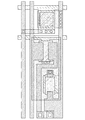
図1(A)及び図1(B)は本発明の一態様のタッチパネルを模式的に示した断面図である。 1A and 1B are cross-sectional views schematically illustrating a touch panel of one embodiment of the present invention.
基板100上に下地膜101及び薄膜トランジスタ102が形成されている。薄膜トランジスタ102は、例えばゲート電極103、ゲート絶縁膜104、第1の半導体層105、第2の半導体層(半導体層106及び半導体層107)、導電層108、導電層109で構成される。図1(A)及び図1(B)では、導電層108及び導電層109と同材料でタッチセンサの下部電極110が形成されている。下部電極110は、薄膜トランジスタ102を構成する材料のうちいずれか一つを用いて形成すればよく、上記材料に限定されない。
A
薄膜トランジスタ102を覆うように絶縁層111が形成されている。タッチセンサの下部電極110上には充填層112が形成されている。EL素子の第1の電極113と導電層108とを電気的に接続する配線114が形成されている。第1の電極113と同材料でタッチセンサの上部電極115が形成されている。なお、充填層112は変形可能な多孔質材料や弾性を有する絶縁性材料を用いることができる。また、第1の電極113と配線114とは同材料を用いて同時に形成することも可能である。
An insulating layer 111 is formed so as to cover the
図1(A)に示すように、充填層112は上部に膨らみを有していてもよい。また、図1(B)に示すように、充填層112の上部が平坦であってもよい。
As shown in FIG. 1A, the
さらに、第1の電極113の端部及び上部電極115を覆い、且つ、上部電極115に達する開口を有する隔壁116が形成されている。前記開口にはスペーサ117が形成されている。スペーサ117は、上部電極115を介して下部電極110及び充填層112と重なる位置に設けられている。第1の電極113に接してEL層118が形成され、EL層118及び隔壁116上に第2の電極119が形成されている。
Further, a
ここで、充填層112、隔壁116、及びスペーサ117に用いる材料のうち、スペーサ117に用いる材料が最も硬い材料であり、充填層112に用いる材料が最も柔らかい材料である。硬さ及び柔らかさを示すものとして、弾性率などがあげられる。弾性率は変形しにくさを表す物性値である。弾性率で硬さ及び柔らかさを表す場合には、スペーサ117に用いる材料の弾性率は隔壁116に用いる材料の弾性率よりも高く、隔壁116に用いる材料の弾性率は充填層112に用いる材料の弾性率よりも高いといえる。
Here, among the materials used for the
続いて封止を行う。例えば、薄膜トランジスタ102等が形成された素子基板120の端部にシール材(図示しない)を設け、シール材によって素子基板120と封止基板121とを貼り合わせることによって封止する。図1(A)及び図1(B)に示すタッチパネルは、素子基板120、封止基板121、及びシール材で囲まれた空間122に面して発光素子が備えられた構造になっている。空間122には、不活性気体(例えば窒素やアルゴン等)が充填される。また、不活性気体の代わりにシール材を充填してもよい。
Subsequently, sealing is performed. For example, a sealing material (not shown) is provided at an end portion of the
次に、タッチパネルに指が接触した時の様子を図2に示す。 Next, FIG. 2 shows a state when a finger touches the touch panel.
図2のように、封止基板121の表面を指123で触れると、封止基板121が撓む。このとき、隔壁116の上部が押されて凹むが、隔壁116に用いる材料よりも硬い(弾性率が高い)スペーサ117が下に押し下げられる。スペーサ117の下層に設けられた充填層112は、スペーサ117よりも柔らかい(弾性率が低い)ため、スペーサ117は変形することなく下に押し下げられる。スペーサ117が下に押し下げられることによって、タッチセンサの上部電極115の位置が下に下がるので、タッチセンサの下部電極110と上部電極115とが接触する、もしくは下部電極110と上部電極115との距離に変化が生じる。これにより、データを入力することができる。
As shown in FIG. 2, when the surface of the sealing
本発明の一態様によれば、タッチセンサが発光素子と並置されているため、発光素子の上若しくは下にタッチセンサが設けられた場合と比べて、画質劣化の少ない、薄型のタッチパネルを提供することができる。 According to one embodiment of the present invention, since a touch sensor is juxtaposed with a light-emitting element, a thin touch panel with less deterioration in image quality compared with the case where a touch sensor is provided above or below the light-emitting element is provided. be able to.
本発明の一態様によれば、充填層、隔壁、及びスペーサに硬さの異なる材料を用いることによって、効率的にタッチセンサに入力ができ、且つ、発光素子に圧力が加わりにくい構造のタッチパネルを提供することができる。また、スペーサをタッチセンサの上部に設けることで、タッチセンサの耐久度及びセンサ感度を向上することができる。 According to one embodiment of the present invention, a touch panel having a structure in which a material having different hardness is used for a filling layer, a partition wall, and a spacer can efficiently input to a touch sensor and pressure is not easily applied to a light emitting element. Can be provided. Moreover, the durability and sensor sensitivity of a touch sensor can be improved by providing a spacer in the upper part of a touch sensor.
なお、本実施の形態は、本明細書の他の実施の形態で示した構成と適宜組み合わせて実施することができる。 Note that this embodiment can be implemented in appropriate combination with the structures described in the other embodiments in this specification.
(実施の形態2)
本実施の形態では、静電容量方式のタッチパネルの動作について説明する。
(Embodiment 2)
In this embodiment, an operation of a capacitive touch panel is described.
静電容量方式のタッチセンサは、上部電極と下部電極との距離の変化によってデータが入力される。本発明の一態様は、タッチセンサとして微小構造体(MEMS)を用いる。 In the capacitive touch sensor, data is input by a change in the distance between the upper electrode and the lower electrode. One embodiment of the present invention uses a microstructure (MEMS) as a touch sensor.
タッチセンサの構造は、図1(A)、図1(B)、及び図2に示したとおりであるため、ここでは省略する。 Since the structure of the touch sensor is as shown in FIGS. 1A, 1B, and 2, it is omitted here.
静電容量方式のタッチパネルは、上部電極と下部電極との間に誘電体となる絶縁性材料が設けられている。充填層112には、変形可能な多孔質材料や弾性を有する絶縁性材料を用いており、これが誘電体となる。
In the capacitive touch panel, an insulating material serving as a dielectric is provided between the upper electrode and the lower electrode. The
図3(A)は、静電容量方式のタッチパネルの一画素の一態様を示したものである。図3(A)の上面図は、図12又は図22に一例として示している。 FIG. 3A illustrates one mode of one pixel of a capacitive touch panel. The top view of FIG. 3A is shown as an example in FIG.
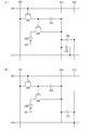
スイッチング用トランジスタ200のゲートは、ゲート線201に電気的に接続している。スイッチング用トランジスタ200のソース及びドレインの一方は、ソース線202に電気的に接続している。第1の容量素子203の第1の端子は、スイッチング用トランジスタ200のソース及びドレインの他方に電気的に接続している。第1の容量素子203の第2の端子は、電源線204に電気的に接続している。駆動用トランジスタ205のゲートは、スイッチング用トランジスタ200のソース及びドレインの他方に電気的に接続している。駆動用トランジスタ205のソース及びドレインの一方は、発光素子206の一方の電極に電気的に接続している。発光素子206の他方の電極は、電源線207に電気的に接続している。駆動用トランジスタ205のソース及びドレインの他方は、電源線204に電気的に接続している。第2の容量素子208の第1の端子は、電源線204に電気的に接続している。第2の容量素子208の第2の端子は、カラム線209に電気的に接続している。第3の容量素子210の第1の端子は、電源線204に電気的に接続している。第3の容量素子210の第2の端子は、ロー線211に電気的に接続している。なお、第2の容量素子208及び第3の容量素子210は、タッチパネルに指等が接触することにより、容量値が変化する容量素子である。ここでは、駆動用トランジスタ205としてp型トランジスタを図示したが、n型トランジスタを用いてもよい。
The gate of the switching
図4は、タッチパネルに指等が接触した位置を検出するためのカラム線(x座標検出線)及びロー線(y座標検出線)を示したものである。カラム線209は、図4に示すx1〜xn(nは1以上の整数)のいずれか一であり、ロー線211は、図4に示すy1〜ym(mは1以上の整数)のいずれか一である。
FIG. 4 shows a column line (x coordinate detection line) and a row line (y coordinate detection line) for detecting a position where a finger or the like touches the touch panel. The
タッチセンサは上部電極、誘電体(本発明の一態様においては充填層)、及び下部電極からなる。タッチセンサの容量値は、充填層に用いた材料の誘電率と、上部電極あるいは下部電極の面積と、上部電極と下部電極との距離とによって決まる。上部電極と下部電極との距離が縮まると、容量値は大きくなる。上部電極と下部電極との距離が広がると、容量値は小さくなる。 The touch sensor includes an upper electrode, a dielectric (a filling layer in one embodiment of the present invention), and a lower electrode. The capacitance value of the touch sensor is determined by the dielectric constant of the material used for the filling layer, the area of the upper electrode or the lower electrode, and the distance between the upper electrode and the lower electrode. As the distance between the upper electrode and the lower electrode decreases, the capacitance value increases. As the distance between the upper electrode and the lower electrode increases, the capacitance value decreases.
また、タッチセンサにたまる電荷量は、容量値と、上部電極と下部電極との間の電圧とを掛け合わせたものである。上部電極と下部電極との間の電圧は変化しないので、上部電極と下部電極との距離が変化したことによって容量値に変化があったとき、タッチセンサにたまる電荷量が変化する。電荷量の変化によってカラム線209及びロー線211に電流が流れるので、電流が流れる先に検出器(検出回路)250を配置しておくことでタッチ位置251を検出することができる。
The amount of charge accumulated in the touch sensor is a product of the capacitance value and the voltage between the upper electrode and the lower electrode. Since the voltage between the upper electrode and the lower electrode does not change, when the capacitance value changes due to a change in the distance between the upper electrode and the lower electrode, the amount of charge accumulated in the touch sensor changes. Since a current flows through the
静電容量方式のタッチパネルは、上部電極と下部電極との距離の変化によってデータが入力される方式であるため、軽くタッチするだけでデータ入力を行うことができる。 Since the capacitive touch panel is a method in which data is input by a change in the distance between the upper electrode and the lower electrode, data can be input only by lightly touching.
なお、本実施の形態は、本明細書の他の実施の形態で示した構成と適宜組み合わせて実施することができる。 Note that this embodiment can be implemented in appropriate combination with the structures described in the other embodiments in this specification.
(実施の形態3)
本実施の形態では、実施の形態2と異なる静電容量方式のタッチパネルの動作について説明する。
(Embodiment 3)
In this embodiment, an operation of a capacitive touch panel different from that in Embodiment 2 is described.
図3(B)は、静電容量方式のタッチパネルの一画素の一態様を示したものである。図3(B)の上面図は、図13又は図23に一例として示している。 FIG. 3B illustrates one mode of one pixel of a capacitive touch panel. The top view of FIG. 3B is shown as an example in FIG. 13 or FIG.
スイッチング用トランジスタ200、ゲート線201、ソース線202、第1の容量素子203、電源線204、駆動用トランジスタ205、発光素子206、及び電源線207については、図3(A)と同様である。第2の容量素子212の第1の端子は、電源線204に電気的に接続している。第2の容量素子212の第2の端子は、カラム線213に電気的に接続している。カラム線213は、ロー線214と電気的に接続している。
The switching
図3(A)では容量値が変化する容量素子(タッチセンサ)が2つ存在したが、図3(B)では、容量値が変化する容量素子(タッチセンサ)は1つであり、タッチパネルに指等が接触した位置を検出するためのカラム線(x座標検出線)とロー線(y座標検出線)とが電気的に接続している。したがって、図3(A)の構成では、タッチ位置をx座標、y座標それぞれで検出するが、図3(B)の構成では、x座標及びy座標を1つのタッチセンサで検出する。 In FIG. 3A, there are two capacitive elements (touch sensors) whose capacitance value changes, but in FIG. 3B, there is one capacitive element (touch sensor) whose capacitance value changes, and the touch panel A column line (x coordinate detection line) and a row line (y coordinate detection line) for detecting a position touched by a finger or the like are electrically connected. Therefore, in the configuration of FIG. 3A, the touch position is detected by the x-coordinate and the y-coordinate, but in the configuration of FIG. 3B, the x-coordinate and the y-coordinate are detected by one touch sensor.
静電容量方式のタッチパネルは、上部電極と下部電極との距離の変化によってデータが入力される方式であるため、軽くタッチするだけでデータ入力を行うことができる。 Since the capacitive touch panel is a method in which data is input by a change in the distance between the upper electrode and the lower electrode, data can be input only by lightly touching.
なお、本実施の形態は、本明細書の他の実施の形態で示した構成と適宜組み合わせて実施することができる。 Note that this embodiment can be implemented in appropriate combination with the structures described in the other embodiments in this specification.
(実施の形態4)
本実施の形態では、抵抗膜方式のタッチパネルの動作について説明する。
(Embodiment 4)
In this embodiment mode, operation of a resistive touch panel is described.
抵抗膜方式のタッチセンサは、上部電極と下部電極との接触によりデータが入力される。本発明の一態様は、タッチセンサとして微小構造体(MEMS)を用いる。 In the resistive touch sensor, data is input by contact between the upper electrode and the lower electrode. One embodiment of the present invention uses a microstructure (MEMS) as a touch sensor.
タッチセンサの構造は、図1(A)及び図1(B)、図2に示したとおりであるため、ここでは省略する。 Since the structure of the touch sensor is as shown in FIGS. 1A, 1B, and 2, it is omitted here.
抵抗膜方式のタッチパネルは、上部電極と下部電極との間に絶縁性材料が設けられている。充填層112には、変形可能な多孔質材料や弾性を有する絶縁性材料を用いるとよい。
In the resistive touch panel, an insulating material is provided between the upper electrode and the lower electrode. For the
図5(A)は抵抗膜方式のタッチパネルの一画素の一態様を示したものである。図5(A)の上面図は、図12又は図22に一例として示している。 FIG. 5A illustrates one mode of one pixel of a resistive film type touch panel. The top view of FIG. 5A is shown as an example in FIG.
スイッチング用トランジスタ300のゲートは、ゲート線301に電気的に接続している。スイッチング用トランジスタ300のソース及びドレインの一方は、ソース線302に電気的に接続している。容量素子303の第1の端子は、スイッチング用トランジスタ300のソース及びドレインの他方に電気的に接続している。容量素子303の第2の端子は、電源線304に電気的に接続している。駆動用トランジスタ305のゲートは、スイッチング用トランジスタ300のソース及びドレインの他方に電気的に接続している。駆動用トランジスタ305のソース及びドレインの一方は、発光素子306の一方の電極に電気的に接続している。発光素子306の他方の電極は、電源線307に電気的に接続している。駆動用トランジスタ305のソース及びドレインの他方は、電源線304に電気的に接続している。スイッチ308の第1の端子は、電源線304に電気的に接続している。スイッチ308の第2の端子は、カラム線309に電気的に接続している。スイッチ308の第3の端子は、ロー線310に電気的に接続している。ここでは、駆動用トランジスタ305としてp型トランジスタを図示したが、n型トランジスタを用いてもよい。
The gate of the switching
図6は、タッチパネルに指等が接触した位置(タッチ位置351)を検出するためのカラム線(x座標検出線)及びロー線(y座標検出線)を示したものである。 FIG. 6 shows column lines (x coordinate detection lines) and row lines (y coordinate detection lines) for detecting a position (touch position 351) where a finger or the like touches the touch panel.
指等でタッチパネルに触れると、上部電極と下部電極とが接触して、カラム線309及びロー線310にそれぞれ接続された検出器350に信号が入力される。検出器が電流計の場合、検出器には電流が流れる。検出器が電圧計の場合、検出器には電圧が印加される。図5(A)においては、x座標をカラム線で、y座標をロー線で検出する。
When the touch panel is touched with a finger or the like, the upper electrode and the lower electrode come into contact with each other, and a signal is input to the
本実施の形態は、本明細書の他の実施の形態で示した構成と適宜組み合わせて実施することができる。 This embodiment can be implemented in appropriate combination with the structures described in the other embodiments in this specification.
(実施の形態5)
本実施の形態では、実施の形態4と異なる抵抗膜方式のタッチパネルの動作について説明する。
(Embodiment 5)
In this embodiment mode, operation of a resistive film type touch panel different from that in Embodiment Mode 4 will be described.
図5(B)は、抵抗膜方式のタッチパネルの一画素の一態様を示したものである。図5(B)の上面図は、図14又は図24に一例として示している。 FIG. 5B illustrates one mode of one pixel of a resistive film type touch panel. The top view of FIG. 5B is shown as an example in FIG.
スイッチング用トランジスタ300、ゲート線301、ソース線302、容量素子303、電源線304、駆動用トランジスタ305、発光素子306、及び電源線307については、図5(A)と同様である。スイッチ311の第1の端子は、カラム線312に電気的に接続している。スイッチ311の第2の端子は、電源線313に電気的に接続している。図5(A)ではタッチセンサの上部電極が電源線304に電気的に接続しているが、図5(B)では接続していない。
The switching
指等でタッチパネルに触れると、上部電極が下部電極に接触して、カラム線312に接続された検出器に電源線313から信号が入力される。電源線313の電位や検出器の構成はx座標及びy座標を検出できるよう工夫が必要である。これにより、タッチ位置を知ることができる。
When the touch panel is touched with a finger or the like, the upper electrode comes into contact with the lower electrode, and a signal is input from the
本実施の形態は、本明細書の他の実施の形態で示した構成と適宜組み合わせて実施することができる。 This embodiment can be implemented in appropriate combination with the structures described in the other embodiments in this specification.
(実施の形態6)
本実施の形態では、図1(A)及び図1(B)に示した充填層112に用いる材料について説明する。実施の形態1に記載したように、充填層112には、変形可能な多孔質材料や弾性を有する絶縁性材料を用いることができる。
(Embodiment 6)
In this embodiment, materials used for the
変形可能な多孔質材料としては、形成後に所定の処理(例えば熱処理や薬液処理等)を行うことにより、軟化又は硬化する材料が好ましい。このような材料として、例えばミクロ相分離構造を形成する、ブロックコポリマー又はグラフトコポリマーを用いることができる。 As the deformable porous material, a material that is softened or hardened by performing a predetermined treatment (for example, heat treatment or chemical treatment) after formation is preferable. As such a material, for example, a block copolymer or a graft copolymer that forms a microphase-separated structure can be used.
ブロックコポリマーとは、複数のホモポリマー鎖がブロックとして結合した直鎖コポリマーをいう。例えば、ジブロックコポリマーが挙げられる。また、トリブロックコポリマーに代表される、3種以上のポリマー鎖が結合したブロックコポリマーを用いてもよい。 The block copolymer refers to a linear copolymer in which a plurality of homopolymer chains are bonded as a block. For example, a diblock copolymer is mentioned. Moreover, you may use the block copolymer which 3 or more types of polymer chains couple | bonded represented by the triblock copolymer.
グラフトコポリマーとは、ポリマーの主鎖に、他のポリマー鎖が側鎖として結合した構造のコポリマーをいう。側鎖として結合するポリマー鎖は、異なる種類のものであってもよい。 The graft copolymer refers to a copolymer having a structure in which another polymer chain is bonded as a side chain to the main chain of the polymer. Different types of polymer chains may be bonded as side chains.
充填層112を形成する材料としては、ブロックコポリマーを用いることが好ましい。ブロックコポリマーは、分子量分布の狭いポリマーを得やすく、組成比の制御も比較的容易だからである。充填層112を形成する材料の組成比を制御することで、充填層112の単位体積あたりに空孔が占める体積を制御することができる。そのため、単位荷重あたりの充填層112の変形量を異ならせることができる。以下に、本発明の一態様に適用することのできるブロックコポリマーについて説明する。
As a material for forming the
ブロックコポリマーは、ナノメートルスケールのミクロ相分離構造を自発的に形成することが知られている。例えば、AB型ブロックコポリマーではミクロ相分離により、ブロックコポリマーを構成する高分子の組成比に応じて、球構造、シリンダー構造、ジャイロイド構造又はラメラ構造といった周期構造を形成する。なお、一方の成分の比率が概ね20%以下で球構造(図7(A)又は図7(E))となり、概ね20%以上35%以下でシリンダー構造(図7(B)又は図7(D))となり、概ね35%以上40%以下でジャイロイド構造(図7(F)又は図7(G))となり、概ね40%以上でラメラ構造(図7(C))となる。なお、球構造では、ウエットエッチングにおいて薬液が達し難く、除去すべき一方の材料の除去が困難なため、シリンダー構造、ジャイロイド構造又はラメラ構造とすることが好ましい。 Block copolymers are known to spontaneously form nanometer-scale microphase separation structures. For example, in the AB type block copolymer, a periodic structure such as a spherical structure, a cylinder structure, a gyroid structure, or a lamellar structure is formed by microphase separation according to the composition ratio of the polymers constituting the block copolymer. When the ratio of one component is approximately 20% or less, a spherical structure (FIG. 7 (A) or FIG. 7 (E)) is obtained, and when approximately 20% or more and 35% or less, the cylinder structure (FIG. 7 (B) or FIG. D)), the gyroid structure (FIG. 7 (F) or FIG. 7 (G)) is approximately 35% to 40%, and the lamella structure (FIG. 7 (C)) is approximately 40% or more. In the spherical structure, the chemical solution is difficult to reach in wet etching, and it is difficult to remove one of the materials to be removed. Therefore, a cylindrical structure, a gyroidal structure, or a lamellar structure is preferable.
ブロックコポリマーの作製には、例えばリビング重合法を用いることができる。リビング重合法は、アニオン又はカチオンを生成する重合開始剤により一種のモノマーの重合を開始させ、他のモノマーを逐次的に添加することによって合成し、ブロックコポリマーを作製する方法である。その作製方法について以下に説明する。 For production of the block copolymer, for example, a living polymerization method can be used. The living polymerization method is a method of preparing a block copolymer by starting polymerization of one type of monomer with a polymerization initiator that generates an anion or a cation, and sequentially adding other monomers. The manufacturing method will be described below.
まず、ブロックコポリマーを構成する材料を溶媒に溶解させる。この溶媒は、ブロックコポリマーを構成する複数種のポリマーのすべてに対して良溶媒であることが好ましい。ここで、良溶媒とは、ブロックコポリマーを構成するポリマーの均一溶液を作製することができる溶媒をいう。ここでは、2種類のポリマーを用いるため、2種類のポリマーの均一溶液を作製できればよい。例えば、ブロックコポリマーの約5重量%のトルエン溶液を、スピンコート法等により充填層112が形成される領域に塗布する。なお、スピンコート法では溶液が基板全面に塗布されるが、例えば液滴吐出法を用いることで所望の領域にのみ溶液が塗布されるため、後の工程が簡素化し、更には材料の利用効率が向上する。
First, the material constituting the block copolymer is dissolved in a solvent. This solvent is preferably a good solvent for all of the plural types of polymers constituting the block copolymer. Here, the good solvent means a solvent capable of producing a uniform solution of a polymer constituting the block copolymer. Here, since two types of polymers are used, it is sufficient that a uniform solution of two types of polymers can be produced. For example, a toluene solution of about 5% by weight of a block copolymer is applied to a region where the
次に、該溶液が塗布された基板に対して加熱処理を行い、ミクロ相分離を誘起する。加熱処理の温度は、ブロックコポリマーを構成する成分のガラス転移点以上であり、且つ相転移温度以下に設定する。 Next, the substrate coated with the solution is subjected to heat treatment to induce microphase separation. The temperature of the heat treatment is set to be equal to or higher than the glass transition point of the component constituting the block copolymer and equal to or lower than the phase transition temperature.
なお、ブロックコポリマーには様々な種類があるが、代表的にはスチレン−ブタジエン系AB型又はスチレン−イソプレン系AB型が挙げられる。その他には、PMMA(Polymetylmethacrylate)のブロックコポリマー等の、異なる材料により構成されたブロックコポリマーや、スチレン−イソプレン系のブロックコポリマーの末端に修飾基をつけたもの等がある。ブロックコポリマーの高分子セグメントとしては、例えば、ポリスチレン若しくはポリフルオレン等の疎水性芳香族炭化水素鎖、ポリブタジエン若しくはポリイソプレン等の疎水性脂肪族不飽和炭化水素鎖、ポリビニルアルコール若しくはポリエチレングリコール等の親水性脂肪族炭化水素鎖、若しくはポリスチレンスルホン酸等の親水性芳香族炭化水素鎖、ポリジメチルシロキサン等の疎水性シロキサン類又はポリフェロセン等の金属錯体等が挙げられる。そして、ブロックコポリマーは、これら高分子セグメントの二種以上が一点以上の結合点において共有結合することによって、線状、分岐状又は環状となっている。 There are various types of block copolymers, and typical examples include styrene-butadiene AB type and styrene-isoprene AB type. In addition, there are block copolymers made of different materials, such as PMMA (Polymethylmethacrylate) block copolymers, and styrene-isoprene block copolymers with a modification group attached to the ends thereof. The polymer segment of the block copolymer includes, for example, a hydrophobic aromatic hydrocarbon chain such as polystyrene or polyfluorene, a hydrophobic aliphatic unsaturated hydrocarbon chain such as polybutadiene or polyisoprene, and a hydrophilic property such as polyvinyl alcohol or polyethylene glycol. Examples include aliphatic hydrocarbon chains, hydrophilic aromatic hydrocarbon chains such as polystyrene sulfonic acid, hydrophobic siloxanes such as polydimethylsiloxane, and metal complexes such as polyferrocene. The block copolymer is linear, branched or cyclic by covalently bonding two or more of these polymer segments at one or more bonding points.
上記の材料には、更に溶媒を含んでいても良い。溶媒としては、例えば、ヘキサン、ヘプタン若しくはオクタン等の脂肪族炭化水素、四塩化炭素、クロロホルム若しくはジクロロメタン等のハロゲン化炭化水素、ベンゼン、トルエン若しくはキシレン等の芳香族炭化水素、アセトン若しくはメチルエチルケトン等のケトン類、ジメチルエーテル若しくはジエチルエーテル等のエーテル類、メタノール若しくはエタノール等のアルコール類又は水等が挙げられる。これらの溶媒は、形成する材料の性質又は状態に合わせて選択することができる。 The above material may further contain a solvent. Examples of the solvent include aliphatic hydrocarbons such as hexane, heptane, and octane, halogenated hydrocarbons such as carbon tetrachloride, chloroform, and dichloromethane, aromatic hydrocarbons such as benzene, toluene, and xylene, and ketones such as acetone and methyl ethyl ketone. , Ethers such as dimethyl ether or diethyl ether, alcohols such as methanol or ethanol, or water. These solvents can be selected according to the property or state of the material to be formed.
本実施の形態においては、充填層112を形成することができ、ブロックコポリマーを構成する成分の一方をエッチングで選択的に除去することができればよい。また、ABA型やBAB型でも、ブロックコポリマーの組成に応じて、球構造からラメラ構造までの様々な構造を採りうる。なお、上記したように本発明においてはシリンダー構造、ジャイロイド構造又はラメラ構造をとることが好ましい。
In this embodiment mode, it is sufficient that the
なお、本実施の形態において、充填層112に適用することのできる材料は、上記材料に限定されず、複数種の物質からなり、いずれかの物質を後の工程でエッチング等により除去することができる材料であればよい。また、エッチング等で除去される物質は必ずしも一の物質でなくともよいが、エッチング等によりいずれかの物質を除去した後に、充填層112の少なくとも一の物質が除去されずに残存できることが最低限必要である。また、充填層112形成後の工程に耐えうる程度の耐熱性及び耐薬品性を要する。ここで、充填層112に除去されずに残存する物質は、弾性変形が可能な物質であることが好ましい。
Note that in this embodiment, the material that can be applied to the
なお、本実施の形態において、上記したように充填層112はブロックコポリマーにより形成することができる。ブロックコポリマーにより充填層112を形成する場合には、充填層112を構成する一方の材料が占める体積を20%以上80%以下にすることで空隙率を概ね20%以上80%以下にすることができ、充填層112自体の形成又は充填層112が有する空孔の形成を良好に行うことができる。好ましくは空隙率を20%以上60%以下とする。空隙率を20%以上60%以下とすることで、充填層112はシリンダー構造、ジャイロイド構造又はラメラ構造となる。空隙率を20%以上60%以下とすると、シリンダー構造又はジャイロイド構造の場合であっても空孔の占める体積が充填層112の材料の占める体積よりも小さく、充填層112が密になるため、十分な機械的強度を確保することができる。更に好ましくは、空隙率を20%以上35%以下とする。空隙率を20%以上35%以下とすると、充填層112においてこれを構成する材料の占める体積が大きくなり、十分な機械的強度を有するシリンダー構造となるためである。
Note that in this embodiment mode, the
上記説明したように、充填層112は変形可能な多孔質材料により形成することができる。ただし、これに限定されない。例えば、充填層112を弾性を有する絶縁性材料により形成してもよい。弾性を有する絶縁性材料により充填層112を形成する場合について以下に説明する。
As described above, the
弾性を有する絶縁性材料としては、形成後に所定の処理(熱、薬液処理等)を行うことにより、軟化し、又は硬化する材料を用いることが好ましい。このような材料として、例えば、エラストマー又は熱可塑性エラストマーが挙げられる。エラストマー又は熱可塑性エラストマーを用いると、形成が行いやすいため好ましい。 As the insulating material having elasticity, it is preferable to use a material that softens or hardens by performing a predetermined treatment (heat, chemical solution treatment, or the like) after formation. Examples of such a material include an elastomer or a thermoplastic elastomer. It is preferable to use an elastomer or a thermoplastic elastomer because it is easy to form.
なお、エラストマーとは、柔軟性及び反発弾性を有する有機系樹脂材料をいい、そのヤング率が約1.0×10⁶Pa以上1.0×10⁷Pa以下のものをいう。エラストマーの対義語としてプラストマーがある。 The elastomer refers to an organic resin material having flexibility and impact resilience, and has an Young's modulus of about 1.0 × 10 6 Pa to 1.0 × 10 7 Pa. Plastomer is a synonym for elastomer.
充填層112を形成する材料としては、高分子エラストマーを用いることが好ましい。高分子エラストマーとしては、ポリウレタン樹脂、エチレン−酢酸ビニル樹脂、エチレン−エチルアクリレート樹脂、ポリエステル系樹脂、ポリアミド系樹脂、ブタジエンゴム、ブチルゴム、スチレンブタジエンゴム、ニトリルゴム、イソプレンゴム、クロロプレンゴム若しくはシリコーンゴム等の合成ゴム類、又はそれらの変形体が挙げられるが、これらに限定されない。また、これらの材料の一又は複数種を組み合わせてもよいし、可塑剤等を添加して弾性率を調整してもよい。
As a material for forming the
高分子エラストマーの形成方法としては、例えば、含漬法、コーティング法、スクリーン法、グラビア法、スプレー法又は液滴吐出法等を用いればよい。これらの方法により形成する場合には、高分子エラストマーの材料を溶質として含む溶液を形成した後に、エラストマーを固化する必要がある。従って、充填層112として用いる高分子エラストマーは、常温乾燥型エラストマー又は常温架橋型エラストマーであることが好ましい。常温乾燥型エラストマー又は常温架橋型エラストマーを用いると、エラストマーの固化を目的とした処理(加熱処理又は乾燥処理等)が不要であり、作製工程が簡略化するからである。
As a method for forming the polymer elastomer, for example, an impregnation method, a coating method, a screen method, a gravure method, a spray method or a droplet discharge method may be used. When forming by these methods, it is necessary to solidify the elastomer after forming a solution containing a polymer elastomer material as a solute. Therefore, the polymer elastomer used as the
なお、常温乾燥型エラストマー又は常温架橋型エラストマーとしては、常温で乾燥するもの又は常温で架橋を形成するもののみならず、常温よりやや高い温度で乾燥するもの又は常温よりやや高い温度で架橋を形成するものも含まれる。また、常温乾燥型エラストマーにおける溶媒は、沸点が常温と同程度のものよりも常温よりやや高い程度の温度のものを用いることが好ましい。沸点が常温に近いものでは形成時に沸騰が起こる可能性があるからである。例えば、塩化メチレン(沸点:40℃)又はアセトン(沸点:56℃)等よりもベンゼン(沸点:80℃)又はクロロホルム(沸点:61℃)を用いることが好ましい。更には、一定時間以上放置することで蒸発しうる溶媒すべてを用いることができる。 In addition, room temperature drying type elastomers or room temperature cross-linking type elastomers are not only those that dry at room temperature or those that form crosslinking at room temperature, but those that dry at a temperature slightly higher than room temperature, or those that form a bridge at a temperature slightly higher than room temperature. Something to do is also included. Further, it is preferable to use a solvent having a boiling point slightly higher than room temperature rather than a solvent having a boiling point similar to that of room temperature. This is because if the boiling point is close to room temperature, boiling may occur during formation. For example, it is preferable to use benzene (boiling point: 80 ° C.) or chloroform (boiling point: 61 ° C.) rather than methylene chloride (boiling point: 40 ° C.) or acetone (boiling point: 56 ° C.). Furthermore, any solvent that can be evaporated by leaving it to stand for a certain time or longer can be used.
なお、常温とは、一般には概ね15℃以上25℃以下の温度範囲をいうが、本発明はこれに限定されない。常温乾燥型エラストマー又は常温架橋型エラストマーとしては、約0℃以上約100℃以下で乾燥するもの又は約0℃以上約100℃以下で架橋を形成するものを用いればよい。勿論、乾燥又は架橋の形成が上記温度範囲内で低温であることが好ましい。 Note that room temperature generally refers to a temperature range of approximately 15 ° C. to 25 ° C., but the present invention is not limited to this. As the room temperature dry elastomer or the room temperature cross-linkable elastomer, those that dry at about 0 ° C. or more and about 100 ° C. or less, or those that form a cross-link at about 0 ° C. or more and about 100 ° C. or less may be used. Of course, it is preferable that the drying or the formation of the cross-linking is at a low temperature within the above temperature range.
充填層112として用いるエラストマー又は熱可塑性エラストマーの形成方法として、最も好ましくはスピンコーティング法を用いる。スピンコーティング法を用いることで、充填層112の厚さ及び膜質にむらを生じることなく形成できるからである。充填層112の厚さ及び膜質の均一性を高くすることで、充填層112の強度分布におけるむらの発生を防止することができるため、歩留まり及び信頼性が向上し、好ましい。
As a method for forming the elastomer or thermoplastic elastomer used as the
常温乾燥型エラストマーは、常温で揮発する有機溶剤に高分子エラストマーの固形物を溶解させることで作製することができる。例えば、溶剤希釈型ウレタン又は溶剤希釈型アクリル等を用いればよい。 The room temperature dry elastomer can be produced by dissolving a solid polymer elastomer in an organic solvent that volatilizes at room temperature. For example, solvent diluted urethane or solvent diluted acrylic may be used.
常温架橋型エラストマーは、空気中の水分を吸収して硬化する湿気硬化型又は紫外光(UV)、電子ビーム(EB)若しくは可視光等のエネルギーによって硬化するもの(UV硬化型、EB硬化型若しくは可視光硬化型)を用いればよい。可視光硬化型を用いる場合には、可視光を遮断した空間にて所定の処理を行い、エラストマーの硬化時にのみ可視光に暴露すればよい。可視光硬化型を用いることで、既に形成している層に紫外光又は電子ビーム等を照射することなく充填層112を形成することができるため、紫外光又は電子ビーム等を照射するための設備が不要であり、好ましい。これらは、エラストマーを有機溶剤等に溶解させ、またはエラストマーを水に分散させ、または溶剤等の媒体を用いることなく作製することができる。
The room temperature cross-linked elastomer is a moisture curable type that absorbs moisture in the air and cures, or is cured by energy such as ultraviolet light (UV), electron beam (EB), or visible light (UV curable type, EB curable type, or Visible light curing type) may be used. In the case of using a visible light curable type, it is only necessary to perform a predetermined treatment in a space where visible light is blocked and to be exposed to visible light only when the elastomer is cured. By using the visible light curable type, the
高分子エラストマーの固形物を水に分散させて塗布する場合には、均一に形成することが困難である。ソリッドインクは疎水性の成分が多いためである。従って、エラストマーを水に分散させることなく形成することが好ましい。常温架橋型としては、例えば湿気硬化ウレタン樹脂又は紫外線硬化アクリル樹脂等を用いることができる。常温乾燥型エラストマー及び常温架橋型エラストマーでは特に高温にすることなく形成することができ、既に形成している層を変質等させることなく充填層112を形成することができる。
When a polymer elastomer solid is dispersed in water and applied, it is difficult to form it uniformly. This is because solid ink has many hydrophobic components. Therefore, it is preferable to form the elastomer without dispersing it in water. As the room temperature crosslinking type, for example, a moisture-curing urethane resin or an ultraviolet-curing acrylic resin can be used. The room temperature dry elastomer and the room temperature cross-linked elastomer can be formed without particularly increasing the temperature, and the filled
また、エラストマーは所望の形状に加工することが困難であるため熱可塑性エラストマーを用いてもよい。熱可塑性エラストマーを用いることで、成形が容易になるため好ましい。すなわち、様々な形状に加工することや、精度よく加工することが容易になるため好ましい。 Moreover, since it is difficult to process an elastomer into a desired shape, a thermoplastic elastomer may be used. Use of a thermoplastic elastomer is preferable because molding becomes easy. That is, it is preferable because it becomes easy to process into various shapes and to process with high accuracy.
なお、熱可塑性エラストマーとは、常温では柔軟性及び反発弾性等を有し、加熱により塑性を発現するエラストマーをいう。熱可塑性エラストマーには、ウレタン系、スチレン系、ビニル系又はエステル系等があるが、特定の材料に限定されない。または、所定の処理を行うことにより可塑性を発現する材料を用いてもよい。 The thermoplastic elastomer refers to an elastomer that has flexibility and rebound resilience at room temperature and exhibits plasticity upon heating. Thermoplastic elastomers include urethane, styrene, vinyl or ester, but are not limited to specific materials. Alternatively, a material that develops plasticity by performing a predetermined treatment may be used.
なお、充填層112として多孔質材料を用いる場合には、ブロックコポリマーに含まれる材料のいずれかをエッチング除去する必要がある。以下に、ブロックコポリマーに含まれる材料のいずれかをエッチング除去する工程について説明する。
Note that when a porous material is used as the
ブロックコポリマーの一方の成分の除去には、ドライエッチング又はウエットエッチングを用いることができる。例えば、酸素ガス雰囲気におけるRIE(Reactive Ion Etching)法を用いることができる。ブロックコポリマー中における、除去すべき成分と残存させるべき成分との間のエッチングレートが大きく異なる条件を採用することが好ましい。一般に、ポリマーの分子鎖に含まれる単位分子あたりの炭素分子の含有率が高いほどエッチング耐性が高く、セグメントあたりの酸素分子の含有率が高いほどエッチング耐性が低い。例えば、PS−PMMA(Polystyrene−Polymethylmethacrylate)のブロックコポリマーでは、PS(ポリスチレン)が芳香環を含んでいるため炭素分子の含有率が高い。そのためエッチング耐性が高く、PAAM(Polyacrylamide)は酸素分子の含有率が高いためエッチング耐性が低い。RIE法を用いた場合には、一般には、この2種類の間に4倍近いエッチングレートの差がある。 Dry etching or wet etching can be used to remove one component of the block copolymer. For example, an RIE (Reactive Ion Etching) method in an oxygen gas atmosphere can be used. It is preferable to employ a condition in which the etching rate in the block copolymer is greatly different between the component to be removed and the component to be left. In general, the higher the carbon molecule content per unit molecule contained in the polymer molecular chain, the higher the etching resistance, and the higher the oxygen molecule content per segment, the lower the etching resistance. For example, PS-PMMA (Polystyrene-Polymethylmethacrylate) block copolymer has a high carbon molecule content because PS (polystyrene) contains an aromatic ring. Therefore, etching resistance is high, and PAAM (Polyacrylamide) has low etching resistance due to a high content of oxygen molecules. When the RIE method is used, there is generally a difference in etching rate that is nearly four times between the two types.
なお、上記のエッチングに用いるガスは酸素ガスに限定されず、CF4、H2、C2F6、CHF3、CH2F2、CF3Br、NF3、Cl2、CCl4、HBr、SF6等を用いてもよい。 Note that the gas used for the etching is not limited to oxygen gas, and CF 4 , H 2 , C 2 F 6 , CHF 3 , CH 2 F 2 , CF 3 Br, NF 3 , Cl 2 , CCl 4 , HBr, SF 6 or the like may be used.
なお、エッチングレートは、ブロックコポリマーのモノマー単位により決定される。モノマー単位の総原子数をN、モノマー単位の炭素原子数をNc、モノマー単位の酸素原子数をNoと表すと、エッチングレートはN/(Nc−No)に比例することが知られている。 The etching rate is determined by the monomer unit of the block copolymer. It is known that the etching rate is proportional to N / (Nc-No), where N represents the total number of atoms in the monomer unit, Nc represents the number of carbon atoms in the monomer unit, and No represents the number of oxygen atoms in the monomer unit.
しかし、上記のドライエッチング法では、シリンダー構造等の場合には問題ないが、球構造ではエッチングされない部分が多く存在するおそれがある。そこで、球構造の場合には、ウエットエッチング法を用いるとよい。ウエットエッチング法では、形成したブロックコポリマーの材料に応じて一方の成分をエッチングすることが可能であり、且つ他方の成分に対しては、エッチング耐性の高い条件によりエッチングを行えばよい。しかし、上記の事情を勘案して、より好ましくは、充填層112にシリンダー構造、ジャイロイド構造又はラメラ構造を用いる。
However, in the dry etching method described above, there is no problem in the case of a cylinder structure or the like, but there may be many portions that are not etched in the spherical structure. Therefore, in the case of a spherical structure, a wet etching method may be used. In the wet etching method, one component can be etched according to the material of the formed block copolymer, and the other component may be etched under conditions with high etching resistance. However, in consideration of the above circumstances, it is more preferable to use a cylinder structure, a gyroid structure, or a lamella structure for the packed
また、除去すべき成分の除去方法は、必ずしもエッチングに限定されない。可能であれば、除去すべき一方の成分を加熱処理等により蒸発又は昇華させる等により除去しても良い。 Further, the method for removing the component to be removed is not necessarily limited to etching. If possible, one of the components to be removed may be removed by evaporation or sublimation by heat treatment or the like.
ブロックコポリマーを用いた場合には、上記工程により充填層112の作製が完了する。
When the block copolymer is used, the
なお、図1(A)及び(B)において、充填層112は、充填層112に用いる材料を絶縁層111の開口部に充填して形成される。または、充填層112に用いる材料を絶縁層111上に形成した後、所望の形状に加工することによって形成される。
1A and 1B, the
本発明の一態様の微小構造体は、従来の微小構造体とは異なり、上部電極と下部電極との間に変形が可能な材料が充填されている。そのため、中空部を有する従来の微小構造体よりも機械的強度の高い微小構造体を作製することができる。機械的強度が向上することで、作製工程中又は動作中の不良の発生を防ぐことができるため、歩留まりが向上し、信頼性が向上する。 Unlike the conventional microstructure, the microstructure according to one embodiment of the present invention is filled with a deformable material between the upper electrode and the lower electrode. Therefore, a microstructure having higher mechanical strength than a conventional microstructure having a hollow portion can be manufactured. By improving the mechanical strength, it is possible to prevent the occurrence of defects during the manufacturing process or operation, so that the yield is improved and the reliability is improved.
なお、本実施の形態は、本明細書の他の実施の形態で示した構成と適宜組み合わせて実施することができる。 Note that this embodiment can be implemented in appropriate combination with the structures described in the other embodiments in this specification.
(実施の形態7)
本実施の形態では、本発明の一態様であるタッチパネルの構造について、図8〜図12、図15〜図17を用いて説明する。図8〜図12は本発明の一態様であるタッチパネルの一画素分の上面図であり、図15〜図17は図12のA−B断面図である。なお、図の簡略化のため、図8〜12には、ゲート電極402、403、配線404、下部電極405、ロー線(y座標検出線)450、第1の半導体層407及び408、導電層413〜416、カラム線(x座標検出線)451、充填層419、第1の電極420、配線421、及び上部電極422を図示する。また、本実施の形態で説明するタッチパネルは、実施の形態2で説明した静電容量方式のタッチセンサ、又は実施の形態4で説明した抵抗膜方式のタッチセンサを用いたタッチパネルである。
(Embodiment 7)
In this embodiment, a structure of a touch panel which is one embodiment of the present invention will be described with reference to FIGS. 8 to 12 are top views of one pixel of the touch panel which is one embodiment of the present invention, and FIGS. 15 to 17 are cross-sectional views taken along line AB in FIG. For simplification of the drawings, FIGS. 8 to 12
基板400上に下地膜401を形成する(図15(A))。基板400は、バリウムホウケイ酸ガラス、アルミノホウケイ酸ガラス、もしくはアルミノシリケートガラスなど、ヒュージョン法やフロート法で作製されるガラス基板、セラミック基板の他、トランジスタの処理温度に耐えうる耐熱性を有するプラスチック基板等を用いることができる。また、ステンレス合金などの金属基板の表面に絶縁膜を設けた基板を適用しても良い。
A
下地膜401は、酸化シリコン系材料膜又は窒化シリコン系材料膜等により絶縁膜を単層で、又は積層して形成する。なお、酸化シリコン系材料とは、酸素とシリコンとを主成分とする酸化シリコン、又は酸化シリコンが窒素を含有し、且つ、酸素の含有量が窒素の含有量よりも多い酸化窒化シリコンをいう。窒化シリコン系材料とは、窒素とシリコンとを主成分とする窒化シリコン、又は窒化シリコンが酸素を含有し、窒素の含有量が酸素の含有量よりも多い窒化酸化シリコンをいう。
The
下地膜401上にトランジスタを形成する。トランジスタはどのような形状であってもよく、また、どのような方法で作製されていてもよい。本実施の形態ではボトムゲート型(逆スタガ型)構造であり、特にチャネルエッチ型と呼ばれる構造のトランジスタについて説明する。
A transistor is formed over the
下地膜401上にゲート電極402及び403、配線404、及び微小構造体(MEMS)の下部電極405を形成する(図8及び図15(A))。下地膜401上に導電膜を形成した後、図8のようにエッチングする。したがって、ゲート電極402及び403、配線404、及び下部電極405は同材料で形成されている。ゲート電極402及び403、配線404、及び下部電極405はチタン、モリブデン、タンタル、クロム、タングステン、アルミニウム、ネオジム、銅、銀、金、白金、ニオブ、シリコン、亜鉛、鉄、バリウム、ゲルマニウムなどの導電性を有する金属もしくは半導体材料、又はこれらの合金材料を用いて、スパッタリング法又はCVD法等により形成することができる。また、2種以上の導電性を有する材料を積層することで形成してもよい。また、ゲート電極402及び403の側面をテーパ形状にエッチングしてもよい。なお、図8において、450はロー線(y座標検出線)である。ロー線450はゲート電極402及び403、配線404、及び下部電極405と同材料で形成される。
ゲート電極402及び403、配線404、及び下部電極405上に絶縁膜406を形成する(図15(A))。絶縁膜406は酸化シリコン系材料又は窒化シリコン系材料等を用いて、プラズマCVD法又はスパッタリング法等により形成することができる。また、絶縁膜406は高密度プラズマ処理によって形成することもできる。ここで、高密度プラズマ処理とは、プラズマ密度が1×1011cm−3以上、好ましくは1×1011cm−3以上9×1015cm−3以下で、マイクロ波(例えば周波数2.45GHz)等の高周波を用いたプラズマ処理をいう。このような条件でプラズマを発生させると、低電子温度が0.2eV以上2.0eV以下となる。このように低電子温度の高密度プラズマは、活性種の運動エネルギーが低いためプラズマダメージが少なく、欠陥の少ない膜を形成することを可能とする。このように、高密度プラズマ処理により形成された絶縁膜は、当該絶縁膜と絶縁膜に接触する層との間の界面状態が良好になる。そのため、高密度プラズマ処理を用いて絶縁膜406を形成すると、半導体層との界面状態を良好にすることができる。その結果、半導体素子の電気的特性を向上させることができる。
An insulating
絶縁膜406上に第1の半導体層407及び408を形成する(図9及び図15(A))。第1の半導体層407は、絶縁膜406を介してゲート電極402と重なる位置に形成する。第1の半導体層408は、絶縁膜406を介してゲート電極403と重なる位置に形成する。第1の半導体層407及び408は、アモルファスシリコン(a−Si:H)等の非結晶性を有する半導体層、微結晶シリコン(μ−Si:H)、多結晶シリコン、単結晶シリコン、ヒ化ガリウム(GaAs)等の化合物半導体又は酸化亜鉛(ZnO)、In−Ga−Zn−O系等の酸化物半導体等を用いて、フォトリソグラフィ法、インクジェット法又は印刷法等により形成することができる。なお、第1の半導体層407及び408は、トランジスタのチャネル領域として機能する部分を含む。
First semiconductor layers 407 and 408 are formed over the insulating film 406 (FIGS. 9 and 15A). The
アモルファスシリコン(a−Si:H)または微結晶シリコンを第1の半導体層407及び408として用いる場合は、トランジスタの特性の均一性が高く、かつ、製造コストが小さいという利点がある。特に、対角の長さが500mmを超えるような大型の基板にトランジスタを作製する場合に有効である。 In the case where amorphous silicon (a-Si: H) or microcrystalline silicon is used for the first semiconductor layers 407 and 408, there is an advantage in that uniformity of transistor characteristics is high and manufacturing cost is low. This is particularly effective when a transistor is formed on a large substrate having a diagonal length exceeding 500 mm.
第1の半導体層407及び408として、多結晶シリコンを用いる場合は、トランジスタの移動度が高く、かつ、製造コストが小さいという利点がある。さらに、特性の経年劣化が小さいため、信頼性の高い装置を得ることができる。 In the case where polycrystalline silicon is used for the first semiconductor layers 407 and 408, there is an advantage that the mobility of the transistor is high and the manufacturing cost is low. Furthermore, since the deterioration over time of the characteristics is small, a highly reliable device can be obtained.
第1の半導体層407及び408として、酸化物半導体を用いる場合は、アモルファスシリコンを用いた薄膜トランジスタよりも高い電界効果移動度を得ることができる。酸化物半導体膜はスパッタ法などによって300℃以下の温度で膜形成が可能であり、多結晶シリコンを用いた薄膜トランジスタよりも製造工程が簡単である。 In the case where an oxide semiconductor is used for the first semiconductor layers 407 and 408, higher field-effect mobility than a thin film transistor using amorphous silicon can be obtained. An oxide semiconductor film can be formed at a temperature of 300 ° C. or lower by a sputtering method or the like, and the manufacturing process is simpler than that of a thin film transistor using polycrystalline silicon.
なお、本明細書中で用いることができる酸化物半導体の一例としては、InMO3(ZnO)m(m>0)で表記されるものがある。ここで、Mは、ガリウム(Ga)、鉄(Fe)、ニッケル(Ni)、マンガン(Mn)及びコバルト(Co)から選ばれた一の金属元素又は複数の金属元素を示す。例えばMとしてGaが選択される場合には、Gaのみの場合の他に、GaとNiや、GaとFeなど、Ga以外の上記金属元素が選択される場合を含む。また、上記酸化物半導体において、Mとして含まれる金属元素の他に、不純物元素としてFe、Niその他の遷移金属元素、又は該遷移金属の酸化物が含まれているものがある。本明細書においては、上記酸化物半導体のうち、Mとして少なくともガリウムを含むものをIn−Ga−Zn−O系酸化物半導体と呼び、当該材料を用いた薄膜をIn−Ga−Zn−O系非単結晶膜と呼ぶことがある。 Note that as an example of an oxide semiconductor that can be used in this specification, one represented by InMO 3 (ZnO) m (m> 0) is given. Here, M represents one metal element or a plurality of metal elements selected from gallium (Ga), iron (Fe), nickel (Ni), manganese (Mn), and cobalt (Co). For example, the case where Ga is selected as M includes the case where the above metal element other than Ga, such as Ga and Ni or Ga and Fe, is selected in addition to the case of Ga alone. In addition to the metal element contained as M, some of the above oxide semiconductors contain Fe, Ni, other transition metal elements, or oxides of the transition metal as impurity elements. In this specification, among the above oxide semiconductors, one containing at least gallium as M is referred to as an In—Ga—Zn—O-based oxide semiconductor, and a thin film using the material is referred to as an In—Ga—Zn—O-based semiconductor. Sometimes called a non-single crystal film.
第1の半導体層407上に第2の半導体層409及び410を形成し、第1の半導体層408上に第2の半導体層411及び412を形成する(図15(A))。第2の半導体層409はソース及びドレインの一方として機能する部分を含む。第2の半導体層410はソース及びドレインの他方として機能する部分を含む。第2の半導体層411はソース及びドレインの一方として機能する部分を含む。第2の半導体層412はソース及びドレインの他方として機能する部分を含む。なお、第2の半導体層としては、リン等を含んだシリコン、第1の半導体層よりも導電率の高い半導体材料、第1の半導体層よりもキャリア濃度の高い酸化物半導体等を用いることができる。第2の半導体層は、その機能により、バッファ層又はn+層と表すこともできる。
Second semiconductor layers 409 and 410 are formed over the
第2の半導体層409、410、411及び412上に導電層413、414、415及び416を形成する(図10及び図15(B))。導電層413はソース及びドレインの一方として機能する部分を含む。導電層414はソース及びドレインの他方として機能する部分を含む。導電層415はソース及びドレインの一方として機能する部分を含む。導電層416はソース及びドレインの他方として機能する部分を含む。導電層413、414、415及び416は、チタン、モリブデン、タンタル、クロム、タングステン、アルミニウム、ネオジム、銅、銀、金、白金、ニオブ、シリコン、亜鉛、鉄、バリウム、ゲルマニウムなどの導電性を有する金属もしくは半導体材料、又はこれらの合金材料を用いて、スパッタリング法又はCVD法等により形成することができる。なお、図10において、451はカラム線(x座標検出線)である。カラム線451は導電層413、414、415及び416と同材料で形成される。
導電層413、414、415及び416上にパッシベーション膜417を形成する(図15(B))。パッシベーション膜417としては窒化シリコン等の絶縁膜を用いることができる。
A
パッシベーション膜417上に絶縁層418を形成する(図15(B))。絶縁層418は、酸化シリコン系材料膜又は窒化シリコン系材料膜により形成する。また、絶縁層418としては、ポリイミド、ポリアミド、アクリル(感光性アクリルを含む)、BCB(ベンゾシクロブテン)といった有機樹脂を用いることもできる。また、絶縁層418は単層構造でも積層構造でもよい。
An insulating
絶縁層418をエッチングすることによって、導電層414の一部及び下部電極405の一部を露出させ、コンタクトホールを形成する。次に、形成したコンタクトホールを埋めるように、充填層419を形成する(図11及び図15(B))。充填層419としては、変形可能な多孔質材料や弾性を有する絶縁性材料が挙げられ、実施の形態6に記載した材料を用いることができる。
By etching the insulating
なお、充填層419は、充填層419に用いる材料を絶縁層418のコンタクトホールに充填して形成される。または、充填層419に用いる材料を絶縁層418上に形成した後、所望の形状に加工することによって形成される。
Note that the
絶縁層418及び充填層419上に導電層を形成し、所望の形状にエッチングすることで第1の電極420、配線421、及び微小構造体(MEMS)の上部電極422となる(図12及び図15(C))。上部電極422は充填層419を介して下部電極405と重なる位置に形成される。第1の電極420、配線421、及び上部電極422はチタン、モリブデン、タンタル、クロム、タングステン、アルミニウム、ネオジム、銅、銀、金、白金、ニオブ、シリコン、亜鉛、鉄、バリウム、ゲルマニウムなどの導電性を有する金属もしくは半導体材料、又はこれらの合金材料を用いて、スパッタリング法又はCVD法等により形成することができる。
A conductive layer is formed over the insulating
第1の電極420の端部を覆い、且つ、上部電極422に達する開口を有する隔壁423を形成する(図15(C))。隔壁423としては、有機樹脂膜、無機絶縁膜、又は有機ポリシロキサンを用いることができる。具体的には、ポリイミド、ポリアミド、ポリイミドアミド、アクリル、ベンゾシクロブテン系樹脂を用いて形成すると良い。特に、感光性の材料を用いて、第1の電極420及び上部電極422上に開口を形成し、その開口の側壁が連続した曲率を持って形成される傾斜面となるように形成することが好ましい。
A
上部電極422に達する隔壁423の開口を埋めるようにスペーサ424を形成する(図15(C))。スペーサ424としては紫外線硬化型樹脂等を用いることができる。具体的には、紫外線硬化型アクリル樹脂等を用いて形成するとよい。なお、スペーサ424は下部電極405と重なる位置に形成する。
A
ここで、充填層419、隔壁423、及びスペーサ424に用いる材料のうち、スペーサ424に用いる材料が最も硬い材料であり、充填層419に用いる材料が最も柔らかい材料である。硬さ及び柔らかさを示すものとして、弾性率などがあげられる。弾性率は変形しにくさを表す物性値である。弾性率で硬さ及び柔らかさを表すならば、スペーサ424に用いる材料の弾性率は隔壁423に用いる材料の弾性率よりも高く、隔壁423に用いる材料の弾性率は充填層419に用いる材料の弾性率よりも高いといえる。
Here, among the materials used for the
第1の電極420上にEL層425を形成する(図15(C))。EL層425には、正孔注入層、正孔輸送層、発光層、電子輸送層、電子注入層、正孔阻止層等が含まれる。EL層425に用いる材料は適宜選択すればよい。
An
EL層425及び隔壁423上に第2の電極426を形成する(図15(C))。第1の電極420、EL層425、及び第2の電極426で発光素子を構成している。第2の電極426は透光性を有する導電性材料により形成することができる。透光性を有する導電性材料としては、インジウム錫酸化物(以下、ITOという)、酸化タングステンを含むインジウム酸化物、酸化タングステンを含むインジウム亜鉛酸化物、酸化チタンを含むインジウム酸化物、酸化チタンを含むインジウム錫酸化物、インジウム亜鉛酸化物、又は酸化シリコンを添加したインジウム錫酸化物等が挙げられる。透光性を有する導電性材料の膜の形成はスパッタリング法又はCVD法等により行えばよいが、特定の方法に限定されるものではない。また、第2の電極426は単層構造でもよいし、積層構造としてもよい。
A
以上の工程により、素子基板が作製できる。続いて、素子基板の端部にシール材(図示せず)を設け、シール材によって素子基板と封止基板427とを貼り合わせることによって封止する(図16)。本発明の一態様であるタッチパネルは、素子基板、封止基板427、及びシール材で囲まれた空間428に発光素子が備えられた構造になっている。空間428には、不活性気体(例えば窒素やアルゴン等)が充填される。また、不活性気体の代わりにシール材を充填してもよい。
Through the above steps, an element substrate can be manufactured. Subsequently, a sealing material (not shown) is provided at the end of the element substrate, and the element substrate and the sealing
なお、シール材にはエポキシ系樹脂を用いるのが好ましい。また、これらの材料はできるだけ水分や酸素を透過しない材料であることが望ましい。また、封止基板427にはガラス基板、FRP(Fiberglass−Reinforced Plastics)、PVF(ポリビニルフロライド)、ポリエステル又はアクリル等からなるプラスチック基板を用いることができる。
In addition, it is preferable to use an epoxy resin for the sealing material. Moreover, it is desirable that these materials are materials that do not transmit moisture and oxygen as much as possible. As the sealing
次に、タッチパネルに指が接触した時の様子を図17に示す。 Next, FIG. 17 shows a state when a finger touches the touch panel.
図17のように、封止基板427を指429で押すと、封止基板427が撓む。このとき、隔壁423の上部が押されて凹むが、隔壁423に用いる材料よりも硬い(弾性率が高い)スペーサ424が下に押し下げられる。スペーサ424の下層に設けられた充填層419は、スペーサ424よりも柔らかい(弾性率が低い)ため、スペーサ424は変形することなく下に押し下げられる。スペーサ424が下に押し下げられることによって、微小構造体(MEMS)の上部電極422の位置が下に下がる。静電容量方式の場合、微小構造体(MEMS)の下部電極405と上部電極422との間の距離が変化することにより、データを入力することができる。抵抗膜方式の場合、微小構造体(MEMS)の下部電極405と上部電極422とが接触することにより、データを入力することができる。
As illustrated in FIG. 17, when the sealing
本発明の一態様によれば、薄膜トランジスタ及び発光素子を作製する工程において、タッチセンサを作製することができる。 According to one embodiment of the present invention, a touch sensor can be manufactured in a process of manufacturing a thin film transistor and a light-emitting element.
本発明の一態様によれば、タッチセンサが発光素子と並置されているため、発光素子の上下にタッチセンサが設けられた場合と比べて、画質劣化の少ない、薄型のタッチパネルを提供することができる。 According to one embodiment of the present invention, since a touch sensor is juxtaposed with a light-emitting element, it is possible to provide a thin touch panel with less deterioration in image quality compared to the case where touch sensors are provided above and below the light-emitting element. it can.
本発明の一態様によれば、充填層、隔壁、及びスペーサに硬さの異なる材料を用いることによって、効率的にタッチセンサに入力ができ、且つ、発光素子に圧力が加わりにくい構造のタッチパネルを提供することができる。また、スペーサをタッチセンサの上部に設けることで、タッチセンサの耐久度及びセンサ感度を向上することができる。 According to one embodiment of the present invention, a touch panel having a structure in which a material having different hardness is used for a filling layer, a partition wall, and a spacer can efficiently input to a touch sensor and pressure is not easily applied to a light emitting element. Can be provided. Moreover, the durability and sensor sensitivity of a touch sensor can be improved by providing a spacer in the upper part of a touch sensor.
なお、本実施の形態は、本明細書の他の実施の形態で示した構成と適宜組み合わせて実施することができる。 Note that this embodiment can be implemented in appropriate combination with the structures described in the other embodiments in this specification.
(実施の形態8)
本実施の形態では、実施の形態7と異なるタッチパネルの構造について、図18〜図22、図25〜図27を用いて説明する。図18〜図22は本発明の一態様であるタッチパネルの一画素分の上面図であり、図25〜図27は図22のC−D断面図である。なお、図の簡略化のため、図18〜図22では、ゲート電極502及び503、配線504、ロー線(y座標検出線)550、第1の半導体層506及び507、導電層512〜515、下部電極516、カラム線(x座標検出線)551、充填層519、第1の電極520、配線521、及び上部電極522を図示する。また、本実施の形態で説明するタッチパネルは、実施の形態2で説明した静電容量方式のタッチセンサ、又は実施の形態4で説明した抵抗膜方式のタッチセンサを用いたタッチパネルである。
(Embodiment 8)
In this embodiment, a structure of a touch panel different from that in Embodiment 7 will be described with reference to FIGS. 18 to 22 and FIGS. 25 to 27. 18 to 22 are top views of one pixel of the touch panel according to one embodiment of the present invention, and FIGS. 25 to 27 are cross-sectional views taken along line CD in FIG. For simplification of the drawings, in FIGS. 18 to 22, the
基板500上に下地膜501を形成する(図25(A))。基板500は、バリウムホウケイ酸ガラス、アルミノホウケイ酸ガラス、もしくはアルミノシリケートガラスなど、ヒュージョン法やフロート法で作製されるガラス基板、セラミック基板の他、トランジスタの処理温度に耐えうる耐熱性を有するプラスチック基板等を用いることができる。また、ステンレス合金などの金属基板の表面に絶縁膜を設けた基板を適用しても良い。
A
下地膜501は、酸化シリコン系材料膜又は窒化シリコン系材料膜等により絶縁膜を単層で、又は積層して形成する。なお、酸化シリコン系材料とは、酸素とシリコンとを主成分とする酸化シリコン、又は酸化シリコンが窒素を含有し、且つ、酸素の含有量が窒素の含有量よりも多い酸化窒化シリコンをいう。窒化シリコン系材料とは、窒素とシリコンとを主成分とする窒化シリコン、又は窒化シリコンが酸素を含有し、窒素の含有量が酸素の含有量よりも多い窒化酸化シリコンをいう。
The
下地膜501上にトランジスタを形成する。トランジスタはどのような形状であってもよく、また、どのような方法で作製されていてもよい。本実施の形態ではボトムゲート型(逆スタガ型)構造であり、特にチャネルエッチ型と呼ばれる構造のトランジスタについて説明する。
A transistor is formed over the
下地膜501上にゲート電極502及び503と、配線504とを形成する(図25(A))。下地膜501上に導電膜を形成した後、図18のようにエッチングする。ゲート電極502及び503と、配線504とはチタン、モリブデン、タンタル、クロム、タングステン、アルミニウム、ネオジム、銅、銀、金、白金、ニオブ、シリコン、亜鉛、鉄、バリウム、ゲルマニウムなどの導電性を有する金属もしくは半導体材料、又はこれらの合金材料を用いて、スパッタリング法又はCVD法等により形成することができる。また、2種以上の導電性を有する材料を積層することで形成してもよい。また、ゲート電極502及び503の側面をテーパ形状にエッチングしてもよい。なお、図18において、550はロー線(y座標検出線)である。ロー線550はゲート電極502及び503と、配線504と同材料で形成される。
ゲート電極502及び503、及び配線504上に絶縁膜505を形成する(図25(A))。絶縁膜505は酸化シリコン系材料又は窒化シリコン系材料等を用いて、プラズマCVD法又はスパッタリング法等により形成することができる。また、絶縁膜505は高密度プラズマ処理によって形成することもできる。ここで、高密度プラズマ処理とは、プラズマ密度が1×1011cm−3以上、好ましくは1×1011cm−3以上9×1015cm−3以下で、マイクロ波(例えば周波数2.45GHz)等の高周波を用いたプラズマ処理をいう。このような条件でプラズマを発生させると、低電子温度が0.2eV以上2.0eV以下となる。このように低電子温度の高密度プラズマは、活性種の運動エネルギーが低いためプラズマダメージが少なく、欠陥の少ない膜を形成することを可能とする。このように、高密度プラズマ処理により形成された絶縁膜は、当該絶縁膜と絶縁膜に接触する層との間の界面状態が良好になる。そのため、高密度プラズマ処理を用いて絶縁膜505を形成すると、半導体層との界面状態を良好にすることができる。その結果、半導体素子の電気的特性を向上させることができる。
An insulating
絶縁膜505上に第1の半導体層506及び507を形成する(図19及び図25(A))。第1の半導体層506は、絶縁膜505を介してゲート電極502と重なる位置に形成する。第1の半導体層507は、絶縁膜505を介してゲート電極503と重なる位置に形成する。第1の半導体層506及び507は、アモルファスシリコン(a−Si:H)等の非結晶性を有する半導体層、微結晶シリコン(μ−Si:H)、多結晶シリコン、単結晶シリコン、ヒ化ガリウム(GaAs)等の化合物半導体又は酸化亜鉛(ZnO)、In−Ga−Zn−O系等の酸化物半導体等を用いて、フォトリソグラフィ法、インクジェット法又は印刷法等により形成することができる。なお、第1の半導体層506及び507は、トランジスタのチャネル領域として機能する部分を含む。
First semiconductor layers 506 and 507 are formed over the insulating film 505 (FIGS. 19 and 25A). The
第1の半導体層506及び507としてアモルファスシリコン(a−Si:H)または微結晶シリコンを用いる場合は、トランジスタの特性の均一性が高く、かつ、製造コストが小さいという利点がある。特に、対角の長さが500mmを超えるような大型の基板にトランジスタを作製する場合に有効である。 In the case where amorphous silicon (a-Si: H) or microcrystalline silicon is used for the first semiconductor layers 506 and 507, there is an advantage that uniformity of transistor characteristics is high and manufacturing cost is low. This is particularly effective when a transistor is formed on a large substrate having a diagonal length exceeding 500 mm.
第1の半導体層506及び507として多結晶シリコンを用いる場合は、トランジスタの移動度が高く、かつ、製造コストが小さいという利点がある。さらに、特性の経年劣化が小さいため、信頼性の高い装置を得ることができる。 In the case where polycrystalline silicon is used for the first semiconductor layers 506 and 507, there are advantages that the mobility of the transistor is high and the manufacturing cost is low. Furthermore, since the deterioration over time of the characteristics is small, a highly reliable device can be obtained.
第1の半導体層506及び507として、酸化物半導体を用いる場合は、アモルファスシリコンを用いた薄膜トランジスタよりも高い電界効果移動度を得ることができる。酸化物半導体膜はスパッタ法などによって300℃以下の温度で膜形成が可能であり、多結晶シリコンを用いた薄膜トランジスタよりも製造工程が簡単である。 In the case where an oxide semiconductor is used for the first semiconductor layers 506 and 507, higher field-effect mobility than a thin film transistor using amorphous silicon can be obtained. An oxide semiconductor film can be formed at a temperature of 300 ° C. or lower by a sputtering method or the like, and the manufacturing process is simpler than that of a thin film transistor using polycrystalline silicon.
なお、本明細書中で用いることができる酸化物半導体の一例としては、InMO3(ZnO)m(m>0)で表記されるものがある。ここで、Mは、ガリウム(Ga)、鉄(Fe)、ニッケル(Ni)、マンガン(Mn)及びコバルト(Co)から選ばれた一の金属元素又は複数の金属元素を示す。例えばMとしてGaが選択される場合には、Gaのみの場合の他に、GaとNiや、GaとFeなど、Ga以外の上記金属元素が選択される場合を含む。また、上記酸化物半導体において、Mとして含まれる金属元素の他に、不純物元素としてFe、Niその他の遷移金属元素、又は該遷移金属の酸化物が含まれているものがある。本明細書においては、上記酸化物半導体のうち、Mとして少なくともガリウムを含むものをIn−Ga−Zn−O系酸化物半導体と呼び、当該材料を用いた薄膜をIn−Ga−Zn−O系非単結晶膜と呼ぶことがある。 Note that as an example of an oxide semiconductor that can be used in this specification, one represented by InMO 3 (ZnO) m (m> 0) is given. Here, M represents one metal element or a plurality of metal elements selected from gallium (Ga), iron (Fe), nickel (Ni), manganese (Mn), and cobalt (Co). For example, the case where Ga is selected as M includes the case where the above metal element other than Ga, such as Ga and Ni or Ga and Fe, is selected in addition to the case of Ga alone. In addition to the metal element contained as M, some of the above oxide semiconductors contain Fe, Ni, other transition metal elements, or oxides of the transition metal as impurity elements. In this specification, among the above oxide semiconductors, one containing at least gallium as M is referred to as an In—Ga—Zn—O-based oxide semiconductor, and a thin film using the material is referred to as an In—Ga—Zn—O-based semiconductor. Sometimes called a non-single crystal film.
第1の半導体層506上に第2の半導体層508及び509を形成し、第1の半導体層507上に第2の半導体層510及び511を形成する(図25(A))。第2の半導体層508はソース及びドレインの一方として機能する部分を含む。第2の半導体層509はソース及びドレインの他方として機能する部分を含む。第2の半導体層510はソース及びドレインの一方として機能する部分を含む。第2の半導体層511はソース及びドレインの他方として機能する部分を含む。なお、第2の半導体層としては、リン等を含んだシリコン、第1の半導体層よりも導電率の高い半導体材料、第1の半導体層よりもキャリア濃度の高い酸化物半導体等を用いることができる。第2の半導体層は、その機能により、バッファ層又はn+層と表すこともできる。
Second semiconductor layers 508 and 509 are formed over the
絶縁膜505及び第2の半導体層508、509、510、511上に導電層512、513、514、515、及び微小構造体(MEMS)の下部電極516を形成する(図20及び図25(B))。導電層512はソース及びドレインの一方として機能する部分を含む。導電層513はソース及びドレインの他方として機能する部分を含む。導電層514はソース及びドレインの一方として機能する部分を含む。導電層515はソース及びドレインの他方として機能する部分を含む。導電層512、513、514、515、及び下部電極516は、チタン、モリブデン、タンタル、クロム、タングステン、アルミニウム、ネオジム、銅、銀、金、白金、ニオブ、シリコン、亜鉛、鉄、バリウム、ゲルマニウムなどの導電性を有する金属もしくは半導体材料、又はこれらの合金材料を用いて、スパッタリング法又はCVD法等により形成することができる。なお、図20において、551はカラム線(x座標検出線)である。カラム線551は導電層512、513、514、515、及び下部電極516と同材料で形成される。
導電層512、513、514、515、及び下部電極516上にパッシベーション膜517を形成する(図25(B))。パッシベーション膜517としては窒化シリコン等を用いることができる。
A
パッシベーション膜517上に絶縁層518を形成する(図25(B))。絶縁層518は、酸化シリコン系材料膜又は窒化シリコン系材料膜により形成する。また、絶縁層518としては、ポリイミド、ポリアミド、アクリル(感光性アクリルを含む)、BCB(ベンゾシクロブテン)といった有機樹脂を用いることもできる。また、絶縁層518は単層構造でも積層構造でもよい。
An insulating
絶縁層518をエッチングすることによって、導電層513及び下部電極516を露出させ、コンタクトホールを形成する。次に、形成したコンタクトホールを埋めるように、充填層519を形成する(図21及び図25(B))。充填層519としては変形可能な多孔質材料や弾性を有する絶縁性材料が挙げられ、実施の形態6に記載した材料を用いることができる。
By etching the insulating
絶縁層518及び充填層519上に導電層を形成し、所望の形状にエッチングすることで第1の電極520、配線521及び微小構造体(MEMS)の上部電極522となる(図22及び図25(C))。上部電極522は充填層519を介して下部電極と重なる位置に形成される。第1の電極520、配線521及び上部電極522はチタン、モリブデン、タンタル、クロム、タングステン、アルミニウム、ネオジム、銅、銀、金、白金、ニオブ、シリコン、亜鉛、鉄、バリウム、ゲルマニウムなどの導電性を有する金属もしくは半導体材料、又はこれらの合金材料を用いて、スパッタリング法又はCVD法等により形成することができる。
A conductive layer is formed over the insulating
第1の電極520の端部を覆い、且つ、上部電極522に達する開口を有する隔壁523を形成する(図25(C))。隔壁523としては、有機樹脂膜、無機絶縁膜、又は有機ポリシロキサンを用いることができる。具体的には、ポリイミド、ポリアミド、ポリイミドアミド、アクリル、ベンゾシクロブテン系樹脂を用いて形成すると良い。特に、感光性の材料を用いて、第1の電極520及び上部電極522上に開口を形成し、その開口の側壁が連続した曲率を持って形成される傾斜面となるように形成することが好ましい。
A
上部電極522に達する隔壁523の開口を埋めるようにスペーサ524を形成する(図25(C))。スペーサ524としては紫外線硬化型樹脂等を用いることができる。具体的には、紫外線硬化型アクリル樹脂等を用いて形成するとよい。なお、スペーサ524は下部電極516と重なる位置に形成する。
A
ここで、充填層519、隔壁523、及びスペーサ524に用いる材料のうち、スペーサ524に用いる材料が最も硬い材料であり、充填層519に用いる材料が最も柔らかい材料である。硬さ及び柔らかさを示すものとして、弾性率などがあげられる。弾性率は変形しにくさを表す物性値である。弾性率で硬さ及び柔らかさを表すならば、スペーサ524に用いる材料の弾性率は隔壁523に用いる材料の弾性率よりも高く、隔壁523に用いる材料の弾性率は充填層519に用いる材料の弾性率よりも高いといえる。
Here, among the materials used for the
第1の電極520上にEL層525を形成する(図25(C))。EL層525には、正孔注入層、正孔輸送層、発光層、電子輸送層、電子注入層、正孔阻止層等が含まれる。EL層525に用いる材料は適宜選択すればよい。
An
EL層525及び隔壁523上に第2の電極526を形成する(図25(C))。第1の電極520、EL層525、及び第2の電極526で発光素子を構成している。第2の電極526は透光性を有する導電性材料により形成することができる。透光性を有する導電性材料としては、インジウム錫酸化物(以下、ITOという)、酸化タングステンを含むインジウム酸化物、酸化タングステンを含むインジウム亜鉛酸化物、酸化チタンを含むインジウム酸化物、酸化チタンを含むインジウム錫酸化物、インジウム亜鉛酸化物、又は酸化シリコンを添加したインジウム錫酸化物等が挙げられる。透光性を有する導電性材料の膜の形成はスパッタリング法又はCVD法等により行えばよいが、特定の方法に限定されるものではない。また、第2の電極526は単層構造でもよいし、積層構造としてもよい。
A
以上の工程により、素子基板が作製できる。続いて、素子基板の端部にシール材(図示せず)を設け、シール材によって素子基板と封止基板527とを貼り合わせることによって封止する(図26)。本発明の一態様であるタッチパネルは、素子基板、封止基板527、及びシール材で囲まれた空間528に発光素子が備えられた構造になっている。空間528には、不活性気体(例えば窒素やアルゴン等)が充填される。また、不活性気体の代わりにシール材を充填してもよい。
Through the above steps, an element substrate can be manufactured. Subsequently, a sealing material (not shown) is provided at an end portion of the element substrate, and sealing is performed by bonding the element substrate and the sealing
なお、シール材にはエポキシ系樹脂を用いるのが好ましい。また、これらの材料はできるだけ水分や酸素を透過しない材料であることが望ましい。また、封止基板527にはガラス基板、FRP(Fiberglass−Reinforced Plastics)、PVF(ポリビニルフロライド)、ポリエステル又はアクリル等からなるプラスチック基板を用いることができる。
In addition, it is preferable to use an epoxy resin for the sealing material. Moreover, it is desirable that these materials are materials that do not transmit moisture and oxygen as much as possible. As the sealing
次に、タッチパネルに指が接触した時の様子を図27に示す。 Next, FIG. 27 shows a state when a finger touches the touch panel.
図27のように、封止基板527を指529で押すと、封止基板527が撓む。このとき、隔壁523の上部が押されて凹むが、隔壁523に用いる材料よりも硬い(弾性率が高い)スペーサ524が下に押し下げられる。スペーサ524の下層に設けられた充填層519は、スペーサ524よりも柔らかい(弾性率が低い)ため、スペーサ524は変形することなく下に押し下げられる。スペーサ524が下に押し下げられることによって、微小構造体(MEMS)の上部電極422の位置が下に下がる。静電容量方式の場合、微小構造体(MEMS)の下部電極516と上部電極522との間の距離が変化することにより、データを入力することができる。抵抗膜方式の場合、微小構造体(MEMS)の下部電極516と上部電極522とが接触することにより、データを入力することができる。
As shown in FIG. 27, when the sealing
本発明の一態様によれば、薄膜トランジスタ及び発光素子を作製する工程において、タッチセンサを作製することができる。 According to one embodiment of the present invention, a touch sensor can be manufactured in a process of manufacturing a thin film transistor and a light-emitting element.
本発明の一態様によれば、タッチセンサが発光素子と並置されているため、発光素子の上下にタッチセンサが設けられた場合と比べて、画質劣化の少ない、薄型のタッチパネルを提供することができる。 According to one embodiment of the present invention, since a touch sensor is juxtaposed with a light-emitting element, it is possible to provide a thin touch panel with less deterioration in image quality compared to the case where touch sensors are provided above and below the light-emitting element. it can.
本発明の一態様によれば、充填層、隔壁、及びスペーサに硬さの異なる材料を用いることによって、効率的にタッチセンサに入力ができ、且つ、発光素子に圧力が加わりにくい構造のタッチパネルを提供することができる。また、スペーサをタッチセンサの上部に設けることで、タッチセンサの耐久度及びセンサ感度を向上することができる。 According to one embodiment of the present invention, a touch panel having a structure in which a material having different hardness is used for a filling layer, a partition wall, and a spacer can efficiently input to a touch sensor and pressure is not easily applied to a light emitting element. Can be provided. Moreover, the durability and sensor sensitivity of a touch sensor can be improved by providing a spacer in the upper part of a touch sensor.
なお、本実施の形態は、本明細書の他の実施の形態で示した構成と適宜組み合わせて実施することができる。 Note that this embodiment can be implemented in appropriate combination with the structures described in the other embodiments in this specification.
(実施の形態9)
本発明の一態様に係るタッチパネルはさまざまな電子機器に適用することができる。電子機器としては、例えば、テレビジョン装置(テレビ、またはテレビジョン受信機ともいう)、コンピュータ用などのモニタ、デジタルカメラ、デジタルビデオカメラなどのカメラ、デジタルフォトフレーム、携帯電話機(携帯電話、携帯電話装置ともいう)、携帯型ゲーム機、携帯情報端末、電子ペーパー、音響再生装置、パチンコ機などの大型ゲーム機などが挙げられる。電子機器の一例を図28に示す。
(Embodiment 9)
The touch panel according to one embodiment of the present invention can be applied to various electronic devices. Examples of the electronic device include a television device (also referred to as a television or a television receiver), a monitor for a computer, a camera such as a digital camera or a digital video camera, a digital photo frame, a mobile phone (a mobile phone or a mobile phone). Large-sized game machines such as portable game machines, portable information terminals, electronic paper, sound reproduction apparatuses, and pachinko machines. An example of the electronic device is illustrated in FIG.
図28(A)は電子書籍600の一例を示している。例えば、電子書籍600は、筐体601及び筐体602の2つの筐体で構成されている。筐体601及び筐体602は、軸部603により一体とされており、該軸部603を軸として開閉動作を行うことができる。このような構成により、紙の書籍のような動作を行うことが可能となる。
FIG. 28A illustrates an example of an
筐体601には表示部604が組み込まれ、筐体602には表示部605が組み込まれている。表示部604および表示部605は本発明の一態様であるタッチセンサを有している。表示部604および表示部605は、続き画面を表示する構成としてもよいし、異なる画面を表示する構成としてもよい。異なる画面を表示する構成とすることで、例えば右側の表示部(図28(A)では表示部604)に文章を表示し、左側の表示部(図28(A)では表示部605)に画像を表示することができる。
A
また、図28(A)では、筐体601に操作部などを備えた例を示している。例えば、筐体601において、電源606、操作キー607、スピーカ608などを備えている。なお、筐体の表示部と同一面にキーボードやポインティングデバイスなどを備える構成としてもよい。また、筐体の裏面や側面に、外部接続用端子(イヤホン端子、USB端子、またはACアダプタおよびUSBケーブルなどの各種ケーブルと接続可能な端子など)、記録媒体挿入部などを備える構成としてもよい。さらに、電子書籍600は、電子辞書としての機能を持たせた構成としてもよい。
FIG. 28A illustrates an example in which the
また、電子書籍600は、無線で情報を送受信できる構成としてもよい。無線により、電子書籍サーバから、所望の書籍データなどを購入し、ダウンロードする構成とすることも可能である。
Further, the
本発明の一態様によれば、発光素子の上又は下にタッチセンサが設けられたものと比べて、画質劣化が少なく、薄型の電子書籍を提供することができる。 According to one embodiment of the present invention, a thin electronic book can be provided with less deterioration in image quality as compared with a case where a touch sensor is provided above or below a light-emitting element.
また、本発明の一態様によれば、充填層、隔壁、及びスペーサに硬さの異なる材料を用いることによって、効率的にタッチセンサに入力することができ、且つ、発光素子に圧力が加わりにくい構造のタッチパネルを提供することができる。また、スペーサをタッチセンサの上部に設けることによって、タッチセンサの耐久度が高く、センサ感度の良い電子書籍を提供することができる。 Further, according to one embodiment of the present invention, by using materials with different hardness for the filling layer, the partition, and the spacer, it is possible to efficiently input to the touch sensor and it is difficult for pressure to be applied to the light-emitting element. A touch panel having a structure can be provided. In addition, by providing the spacer above the touch sensor, an electronic book with high touch sensor durability and high sensor sensitivity can be provided.
図28(B)は、デジタルフォトフレーム700の一例を示している。例えば、デジタルフォトフレーム700は、筐体701に表示部702が組み込まれている。表示部702は、各種画像を表示することが可能であり、例えばデジタルカメラなどで撮影した画像データを表示させることで、通常の写真立てと同様に機能させることができる。
FIG. 28B illustrates an example of a
本発明の一態様であるタッチセンサを適用すると、発光素子の上又は下にタッチセンサが設けられたものと比べて、画質劣化が少なく、薄型のデジタルフォトフレームを提供することができる。 When a touch sensor which is one embodiment of the present invention is applied, a thin digital photo frame can be provided with less deterioration in image quality as compared with a case where a touch sensor is provided above or below a light-emitting element.
また、本発明の一態様によれば、充填層、隔壁、及びスペーサに硬さの異なる材料を用いることによって、効率的にタッチセンサに入力することができ、且つ、発光素子に圧力が加わりにくい構造のタッチパネルを提供することができる。また、スペーサをタッチセンサの上部に設けることによって、タッチセンサの耐久度が高く、センサ感度の良いデジタルフォトフレームを提供することができる。 Further, according to one embodiment of the present invention, by using materials with different hardness for the filling layer, the partition, and the spacer, it is possible to efficiently input to the touch sensor and it is difficult for pressure to be applied to the light-emitting element. A touch panel having a structure can be provided. Further, by providing the spacer above the touch sensor, it is possible to provide a digital photo frame with high touch sensor durability and high sensor sensitivity.
100 基板
101 下地膜
102 薄膜トランジスタ
103 ゲート電極
104 ゲート絶縁膜
105 第1の半導体層
106 半導体層
107 半導体層
108 導電層
109 導電層
110 下部電極
111 絶縁層
112 充填層
113 第1の電極
114 配線
115 上部電極
116 隔壁
117 スペーサ
118 EL層
119 第2の電極
120 素子基板
121 封止基板
122 空間
123 指
200 スイッチング用トランジスタ
201 ゲート線
202 ソース線
203 第1の容量素子
204 電源線
205 駆動用トランジスタ
206 発光素子
207 電源線
208 第2の容量素子
209 カラム線
210 第3の容量素子
211 ロー線
212 第2の容量素子
213 カラム線
214 ロー線
250 検出器(検出回路)
251 タッチ位置
300 スイッチング用トランジスタ
301 ゲート線
302 ソース線
303 容量素子
304 電源線
305 駆動用トランジスタ
306 発光素子
307 電源線
308 スイッチ
309 カラム線
310 ロー線
311 スイッチ
312 カラム線
313 電源線
350 検出器
351 タッチ位置
400 基板
401 下地膜
402 ゲート電極
403 ゲート電極
404 配線
405 下部電極
406 絶縁膜
407 第1の半導体層
408 第1の半導体層
409 第2の半導体層
410 第2の半導体層
411 第2の半導体層
412 第2の半導体層
413 導電層
414 導電層
415 導電層
416 導電層
417 パッシベーション膜
418 絶縁層
419 充填層
420 第1の電極
421 配線
422 上部電極
423 隔壁
424 スペーサ
425 EL層
426 第2の電極
427 封止基板
428 空間
429 指
450 ロー線(y座標検出線)
451 カラム線(x座標検出線)
500 基板
501 下地膜
502 ゲート電極
503 ゲート電極
504 配線
505 絶縁膜
506 第1の半導体層
507 第1の半導体層
508 第2の半導体層
509 第2の半導体層
510 第2の半導体層
511 第2の半導体層
512 導電層
513 導電層
514 導電層
515 導電層
516 下部電極
517 パッシベーション膜
518 絶縁層
519 充填層
520 第1の電極
521 配線
522 上部電極
523 隔壁
524 スペーサ
525 EL層
526 第2の電極
527 封止基板
528 空間
529 指
550 ロー線(y座標検出線)
551 カラム線(x座標検出線)
600 電子書籍
601 筐体
602 筐体
603 軸部
604 表示部
605 表示部
606 電源
607 操作キー
608 スピーカ
700 デジタルフォトフレーム
701 筐体
702 表示部
100
251
451 column line (x coordinate detection line)
500
551 Column line (x coordinate detection line)
600
Claims (7)
前記微小構造体は、下部電極と、前記下部電極と対向して設けられた上部電極と、前記下部電極と前記上部電極との間に設けられた充填層とを有し、
前記下部電極は、前記トランジスタのゲート電極と同材料で形成され、
前記上部電極は、前記発光素子の第1の電極と同材料で形成され、
前記スペーサは、前記発光素子の第1の電極を覆う隔壁よりも硬い材料を用いて、前記上部電極上に前記充填層と重なるように形成され、
前記隔壁は、前記充填層よりも硬い材料で形成されることを特徴とするタッチパネル。 A microstructure, a transistor , a light-emitting element electrically connected to the transistor , and a spacer,
The microstructure has a lower electrode, an upper electrode provided to face the lower electrode, and a filling layer provided between the lower electrode and the upper electrode,
The lower electrode is formed of the same material as the gate electrode of the transistor ,
The upper electrode is formed of the same material as the first electrode of the light emitting element,
The spacer is formed using a material harder than a partition covering the first electrode of the light emitting element so as to overlap the filling layer on the upper electrode,
The touch panel is formed of a material harder than the filling layer.
前記微小構造体は、下部電極と、前記下部電極と対向して設けられた上部電極と、前記下部電極と前記上部電極との間に設けられた充填層とを有し、
前記下部電極は、前記トランジスタのソース電極またはドレイン電極と同材料で形成され、
前記上部電極は、前記発光素子の第1の電極と同材料で形成され、
前記スペーサは、前記発光素子の第1の電極を覆う隔壁よりも弾性率の高い材料を用いて、前記上部電極上に前記充填層と重なるように形成され、
前記隔壁は、前記充填層よりも弾性率の高い材料で形成されることを特徴とするタッチパネル。 A microstructure, a transistor , a light-emitting element electrically connected to the transistor , and a spacer,
The microstructure has a lower electrode, an upper electrode provided to face the lower electrode, and a filling layer provided between the lower electrode and the upper electrode,
The lower electrode is formed of the same material as the source electrode or drain electrode of the transistor ,
The upper electrode is formed of the same material as the first electrode of the light emitting element,
The spacer is formed on the upper electrode so as to overlap the filling layer using a material having a higher elastic modulus than the partition covering the first electrode of the light emitting element.
The touch panel is formed of a material having a higher elastic modulus than the filling layer.
前記充填層は、圧力により可逆変形可能な多孔質の絶縁性材料を含むことを特徴とするタッチパネル。 In claim 1 or claim 2 ,
The packed bed, a touch panel, which comprises an insulating material reversibly deformable porous by pressure.
前記多孔質の絶縁性材料はブロックコポリマーであることを特徴とするタッチパネル。 In claim 3 ,
The touch panel, wherein the porous insulating material is a block copolymer.
前記充填層の空隙率は20%以上80%以下であることを特徴とするタッチパネル。 In any one of Claims 1 thru | or 4,
The touch panel, wherein the filling layer has a porosity of 20% or more and 80% or less.
前記充填層は、圧力により可逆変形可能な弾性を有する絶縁性材料を含むことを特徴とするタッチパネル。 In claim 1 or claim 2 ,
The packed bed, a touch panel, which comprises an insulating material having a reversible deformable elastic by pressure.
前記弾性を有する絶縁性材料はエラストマーまたは熱可塑性エラストマーであることを特徴とするタッチパネル。
In claim 6 ,
The touch panel, wherein the insulating material having elasticity is an elastomer or a thermoplastic elastomer.
Priority Applications (1)
| Application Number | Priority Date | Filing Date | Title |
|---|---|---|---|
| JP2010118946A JP5396335B2 (en) | 2009-05-28 | 2010-05-25 | Touch panel |
Applications Claiming Priority (3)
| Application Number | Priority Date | Filing Date | Title |
|---|---|---|---|
| JP2009128549 | 2009-05-28 | ||
| JP2009128549 | 2009-05-28 | ||
| JP2010118946A JP5396335B2 (en) | 2009-05-28 | 2010-05-25 | Touch panel |
Publications (3)
| Publication Number | Publication Date |
|---|---|
| JP2011008775A JP2011008775A (en) | 2011-01-13 |
| JP2011008775A5 JP2011008775A5 (en) | 2013-06-20 |
| JP5396335B2 true JP5396335B2 (en) | 2014-01-22 |
Family
ID=43218997
Family Applications (1)
| Application Number | Title | Priority Date | Filing Date |
|---|---|---|---|
| JP2010118946A Expired - Fee Related JP5396335B2 (en) | 2009-05-28 | 2010-05-25 | Touch panel |
Country Status (2)
| Country | Link |
|---|---|
| US (2) | US8730186B2 (en) |
| JP (1) | JP5396335B2 (en) |
Families Citing this family (71)
| Publication number | Priority date | Publication date | Assignee | Title |
|---|---|---|---|---|
| JP5210901B2 (en) * | 2008-02-06 | 2013-06-12 | 株式会社半導体エネルギー研究所 | Liquid crystal display |
| JP5100670B2 (en) | 2009-01-21 | 2012-12-19 | 株式会社半導体エネルギー研究所 | Touch panel, electronic equipment |
| JP2011017626A (en) * | 2009-07-09 | 2011-01-27 | Sony Corp | Mechanical quantity detection member and mechanical quantity detection apparatus |
| US8149496B2 (en) * | 2009-12-22 | 2012-04-03 | Qualcomm Mems Technologies, Inc. | Integrated touch for IMOD displays using back glass |
| KR101843559B1 (en) | 2010-11-05 | 2018-03-30 | 가부시키가이샤 한도오따이 에네루기 켄큐쇼 | Display device with imaging function and method for driving the same |
| CN103430134B (en) | 2011-01-19 | 2017-03-29 | Lg伊诺特有限公司 | Touch pad and its manufacture method |
| KR20120089123A (en) * | 2011-02-01 | 2012-08-09 | 삼성디스플레이 주식회사 | Organic light emitting display apparatus |
| KR101721533B1 (en) * | 2011-02-24 | 2017-03-30 | 삼성전자주식회사 | Method and apparatus for adjusting touch sensitivity of touch sensor in portable terminal |
| JP5712746B2 (en) * | 2011-04-06 | 2015-05-07 | セイコーエプソン株式会社 | Sensing device and electronic device |
| CN103765777B (en) | 2011-06-29 | 2017-06-06 | 辛纳普蒂克斯公司 | The high-voltage drive of pressure device in use |
| TWI448952B (en) * | 2011-07-11 | 2014-08-11 | Innolux Corp | Electromagnetic touch panel and method for fabricating the same and electromagnetic touch display device |
| DE102011079737A1 (en) * | 2011-07-25 | 2013-01-31 | BSH Bosch und Siemens Hausgeräte GmbH | Operating device for a household appliance and household appliance |
| DE102011079730B4 (en) * | 2011-07-25 | 2013-04-04 | BSH Bosch und Siemens Hausgeräte GmbH | Operating device for a household appliance and household appliance |
| TWI456262B (en) * | 2011-12-16 | 2014-10-11 | Wintek Corp | Switchable touch stereoscopic image device |
| CN104145240B (en) * | 2012-03-09 | 2017-08-29 | 索尼公司 | Sensor device, input equipment and electronic installation |
| KR101911092B1 (en) | 2012-03-16 | 2018-10-23 | 리쿠아비스타 비.브이. | Electro-wetting dispaly device and method for fabricating the same |
| KR101382119B1 (en) * | 2012-04-19 | 2014-04-09 | 실리콘 디스플레이 (주) | Display device of thin film transistor comprising touch sensor and manufacturing method thereof |
| KR102043370B1 (en) * | 2012-12-18 | 2019-11-13 | 삼성디스플레이 주식회사 | controlling method of user input using pressure sensor unit for flexible display device |
| WO2014143065A1 (en) * | 2013-03-15 | 2014-09-18 | Rinand Solutions Llc | Force-sensitive fingerprint sensing input |
| JP6456598B2 (en) | 2013-04-19 | 2019-01-23 | 株式会社半導体エネルギー研究所 | Display device |
| KR102049443B1 (en) * | 2013-05-15 | 2019-11-28 | 삼성디스플레이 주식회사 | Organic light emitting display device and method of manufacturing thereof |
| JP6851197B2 (en) | 2013-05-30 | 2021-03-31 | ティーケー ホールディングス インク.Tk Holdings Inc. | Multidimensional trackpad |
| JP5686445B2 (en) * | 2013-07-01 | 2015-03-18 | 日本写真印刷株式会社 | Mutual capacitive touch panel |
| JP6286430B2 (en) * | 2013-07-30 | 2018-02-28 | 住友理工株式会社 | Input state detection device |
| US9269914B2 (en) | 2013-08-01 | 2016-02-23 | Semiconductor Energy Laboratory Co., Ltd. | Light-emitting device, electronic device, and lighting device |
| WO2015022940A1 (en) | 2013-08-16 | 2015-02-19 | 株式会社ワコム | Indicator detection device and indicator detection method |
| KR20160043959A (en) * | 2013-08-16 | 2016-04-22 | 가부시키가이샤 와코무 | Pointing device detection sensor and pointing device detection device |
| JP2015055925A (en) * | 2013-09-10 | 2015-03-23 | ソニー株式会社 | Sensor device, method of manufacturing sensor device, display apparatus, and input apparatus |
| US9228907B2 (en) | 2013-11-14 | 2016-01-05 | Nokia Technologies Oy | Flexible device deformation measurement |
| KR102239367B1 (en) * | 2013-11-27 | 2021-04-09 | 가부시키가이샤 한도오따이 에네루기 켄큐쇼 | Touch panel |
| KR101712346B1 (en) * | 2014-09-19 | 2017-03-22 | 주식회사 하이딥 | Touch input device |
| CN104898875A (en) * | 2014-03-07 | 2015-09-09 | 群创光电股份有限公司 | Touch control panel, display panel and strengthening structure for protection base plate |
| TWI518572B (en) * | 2014-03-07 | 2016-01-21 | 群創光電股份有限公司 | Touch panel, display panel, and reinforced structure for protective substrate |
| DE102014104324B4 (en) * | 2014-03-21 | 2022-01-27 | Preh Gmbh | Control element with force sensor |
| TWI687143B (en) * | 2014-04-25 | 2020-03-01 | 日商半導體能源研究所股份有限公司 | Display device and electronic device |
| US10073571B2 (en) | 2014-05-02 | 2018-09-11 | Semiconductor Energy Laboratory Co., Ltd. | Touch sensor and touch panel including capacitor |
| JP6580863B2 (en) | 2014-05-22 | 2019-09-25 | 株式会社半導体エネルギー研究所 | Semiconductor devices, health management systems |
| US10071904B2 (en) | 2014-09-25 | 2018-09-11 | Semiconductor Energy Laboratory Co., Ltd. | Semiconductor device, display module, and electronic device |
| US9698170B2 (en) | 2014-10-07 | 2017-07-04 | Semiconductor Energy Laboratory Co., Ltd. | Semiconductor device, display module, and electronic device |
| US10068927B2 (en) | 2014-10-23 | 2018-09-04 | Semiconductor Energy Laboratory Co., Ltd. | Semiconductor device, display module, and electronic device |
| KR102417266B1 (en) * | 2015-01-27 | 2022-07-05 | 삼성디스플레이 주식회사 | Display device and touch sensing method thereof |
| CN106200030B (en) * | 2015-04-30 | 2019-07-05 | 小米科技有限责任公司 | Liquid crystal display, pressure measurement method and device |
| US9548733B2 (en) * | 2015-05-20 | 2017-01-17 | Ford Global Technologies, Llc | Proximity sensor assembly having interleaved electrode configuration |
| CN106301324B (en) * | 2015-06-05 | 2023-05-09 | 深圳纽迪瑞科技开发有限公司 | Pressure sensing key structure and terminal equipment with same |
| JP6890372B2 (en) * | 2015-06-08 | 2021-06-18 | アルプスアルパイン株式会社 | In-vehicle input device |
| US9630836B2 (en) | 2015-09-30 | 2017-04-25 | Mems Drive, Inc. | Simplified MEMS device fabrication process |
| US9617142B1 (en) | 2015-09-30 | 2017-04-11 | Mems Drive, Inc. | MEMS grid for manipulating structural parameters of MEMS devices |
| US9959004B2 (en) | 2015-11-12 | 2018-05-01 | Microsoft Technology Licensing, Llc | Deformation sensor |
| KR102487053B1 (en) | 2015-12-16 | 2023-01-09 | 엘지디스플레이 주식회사 | Liquid crystal display device |
| KR102466939B1 (en) * | 2015-12-31 | 2022-11-11 | 엘지디스플레이 주식회사 | Touch sensitive device, display device comprising the same and method of manufacturing the same |
| CN105824475B (en) * | 2016-03-31 | 2019-11-26 | 京东方科技集团股份有限公司 | A kind of preparation method of display panel, display device and display panel |
| CN105868729A (en) * | 2016-04-12 | 2016-08-17 | 珠海市魅族科技有限公司 | Press button device and terminal |
| CN106020553B (en) * | 2016-06-03 | 2021-01-12 | 京东方科技集团股份有限公司 | Display panel, manufacturing method thereof and display device |
| US10086700B2 (en) * | 2016-10-20 | 2018-10-02 | Ford Global Technologies, Llc | Illuminated switch |
| CN108133932B (en) * | 2016-12-01 | 2020-04-10 | 京东方科技集团股份有限公司 | Array substrate, manufacturing method thereof and display panel |
| KR20180069165A (en) * | 2016-12-14 | 2018-06-25 | 삼성디스플레이 주식회사 | Touch sensor and display device including the same |
| JP7175551B2 (en) * | 2017-03-24 | 2022-11-21 | シナプティクス インコーポレイテッド | Current-driven display panel and panel display device |
| CN106961269A (en) * | 2017-05-11 | 2017-07-18 | 广东太古电器科技有限公司 | Operating control device |
| CN107193420B (en) * | 2017-05-25 | 2020-06-02 | 京东方科技集团股份有限公司 | Touch device and method for manufacturing same |
| CN107340916B (en) * | 2017-06-30 | 2020-05-08 | 上海天马微电子有限公司 | Display panel and display device |
| CN107247532A (en) * | 2017-07-27 | 2017-10-13 | 业成科技(成都)有限公司 | Touch-screen |
| CN107526480B (en) * | 2017-09-22 | 2020-04-28 | 厦门天马微电子有限公司 | Display panel and display device |
| CN107632738B (en) * | 2017-09-29 | 2023-10-20 | 京东方科技集团股份有限公司 | Touch display panel, manufacturing method thereof and touch display device |
| CN109786399B (en) * | 2017-11-13 | 2022-04-05 | 睿生光电股份有限公司 | Detection device |
| CA2985264A1 (en) * | 2017-11-14 | 2019-05-14 | Vuereal Inc. | Integration of touch and sensing |
| CN109683737B (en) * | 2018-11-23 | 2021-02-26 | 京东方科技集团股份有限公司 | Touch substrate, display substrate and display panel |
| CN109614007B (en) * | 2018-12-12 | 2020-08-11 | 武汉华星光电半导体显示技术有限公司 | Display panel |
| CN110277429B (en) * | 2019-06-20 | 2021-11-16 | 武汉天马微电子有限公司 | Flexible display panel and flexible display device |
| CN111146257B (en) * | 2019-12-19 | 2023-06-02 | 云谷(固安)科技有限公司 | Display panel, manufacturing method thereof and display device |
| CN111600592B (en) * | 2020-05-15 | 2023-06-23 | 业成科技(成都)有限公司 | Capacitive touch key |
| EP4322410A1 (en) * | 2022-08-10 | 2024-02-14 | STMicroelectronics S.r.l. | Microelectromechanical button device and corresponding waterproof user interface element |
Family Cites Families (55)
| Publication number | Priority date | Publication date | Assignee | Title |
|---|---|---|---|---|
| JPH05251705A (en) | 1992-03-04 | 1993-09-28 | Fuji Xerox Co Ltd | Thin-film transistor |
| KR100290993B1 (en) * | 1995-06-13 | 2001-08-07 | 이사오 우치가사키 | Semiconductor device, wiring board for mounting semiconductor and method of production of semiconductor device |
| DE19536250A1 (en) * | 1995-09-28 | 1997-04-03 | Siemens Ag | Microelectronic, integrated sensor and method for producing the sensor |
| JP4170454B2 (en) | 1998-07-24 | 2008-10-22 | Hoya株式会社 | Article having transparent conductive oxide thin film and method for producing the same |
| JP3276930B2 (en) | 1998-11-17 | 2002-04-22 | 科学技術振興事業団 | Transistor and semiconductor device |
| JP2000273236A (en) | 1999-03-25 | 2000-10-03 | Jsr Corp | Hydrophilic porous membrane |
| JP2000331557A (en) | 1999-05-21 | 2000-11-30 | Mimaki Denshi Buhin Kk | Light emitting display device with touch panel sensor |
| JP2001109404A (en) * | 1999-10-01 | 2001-04-20 | Sanyo Electric Co Ltd | El display device |
| US6749733B1 (en) * | 2000-04-10 | 2004-06-15 | Intel Corporation | Materials classifier, method of using, and method of making |
| JP4089858B2 (en) | 2000-09-01 | 2008-05-28 | 国立大学法人東北大学 | Semiconductor device |
| US6465280B1 (en) * | 2001-03-07 | 2002-10-15 | Analog Devices, Inc. | In-situ cap and method of fabricating same for an integrated circuit device |
| JP2002289859A (en) | 2001-03-23 | 2002-10-04 | Minolta Co Ltd | Thin-film transistor |
| JP4773630B2 (en) * | 2001-05-15 | 2011-09-14 | 株式会社デンソー | Diaphragm type semiconductor device and manufacturing method thereof |
| US7061014B2 (en) * | 2001-11-05 | 2006-06-13 | Japan Science And Technology Agency | Natural-superlattice homologous single crystal thin film, method for preparation thereof, and device using said single crystal thin film |
| US6780786B2 (en) * | 2001-11-26 | 2004-08-24 | The Regents Of The University Of California | Method for producing a porous silicon film |
| US7943412B2 (en) * | 2001-12-10 | 2011-05-17 | International Business Machines Corporation | Low temperature Bi-CMOS compatible process for MEMS RF resonators and filters |
| JP4077312B2 (en) | 2001-12-28 | 2008-04-16 | 株式会社東芝 | LIGHT EMITTING DEVICE MANUFACTURING METHOD AND LIGHT EMITTING DEVICE |
| TW576864B (en) | 2001-12-28 | 2004-02-21 | Toshiba Corp | Method for manufacturing a light-emitting device |
| JP4083486B2 (en) * | 2002-02-21 | 2008-04-30 | 独立行政法人科学技術振興機構 | Method for producing LnCuO (S, Se, Te) single crystal thin film |
| JP2003296022A (en) | 2002-04-01 | 2003-10-17 | Pioneer Electronic Corp | Touch panel integrated display device |
| US7429495B2 (en) * | 2002-08-07 | 2008-09-30 | Chang-Feng Wan | System and method of fabricating micro cavities |
| JP4076829B2 (en) * | 2002-09-20 | 2008-04-16 | 株式会社東芝 | Microswitch and manufacturing method thereof |
| KR100470634B1 (en) * | 2002-10-02 | 2005-03-10 | 한국전자통신연구원 | Capacitive micro-electro-mechanical switch and a method of manufacturing the same |
| TW200417929A (en) * | 2002-12-10 | 2004-09-16 | Nissha Printing | Narrow frame type touch panel |
| US6917459B2 (en) * | 2003-06-03 | 2005-07-12 | Hewlett-Packard Development Company, L.P. | MEMS device and method of forming MEMS device |
| JP4108633B2 (en) * | 2003-06-20 | 2008-06-25 | シャープ株式会社 | THIN FILM TRANSISTOR, MANUFACTURING METHOD THEREOF, AND ELECTRONIC DEVICE |
| JP4269806B2 (en) * | 2003-06-30 | 2009-05-27 | カシオ計算機株式会社 | Semiconductor device and manufacturing method thereof |
| CN102856390B (en) * | 2004-03-12 | 2015-11-25 | 独立行政法人科学技术振兴机构 | Comprise the LCD of thin-film transistor or the transition components of OLED display |
| US7282782B2 (en) * | 2004-03-12 | 2007-10-16 | Hewlett-Packard Development Company, L.P. | Combined binary oxide semiconductor device |
| EP1738250A2 (en) * | 2004-04-14 | 2007-01-03 | Koninklijke Philips Electronics N.V. | Touch sensitive display |
| JP4695345B2 (en) * | 2004-05-18 | 2011-06-08 | 株式会社 日立ディスプレイズ | Organic electroluminescence display device |
| US7230198B2 (en) * | 2004-11-12 | 2007-06-12 | Eastman Kodak Company | Flexible sheet for resistive touch screen |
| US7560789B2 (en) * | 2005-05-27 | 2009-07-14 | Semiconductor Energy Laboratory Co., Ltd. | Semiconductor device |
| JP4519804B2 (en) | 2005-05-27 | 2010-08-04 | 株式会社半導体エネルギー研究所 | Method for manufacturing semiconductor device |
| JP2007058071A (en) * | 2005-08-26 | 2007-03-08 | Toshiba Matsushita Display Technology Co Ltd | Liquid crystal display apparatus |
| EP1770788A3 (en) * | 2005-09-29 | 2011-09-21 | Semiconductor Energy Laboratory Co., Ltd. | Semiconductor device having oxide semiconductor layer and manufacturing method thereof |
| KR101112655B1 (en) * | 2005-11-15 | 2012-02-16 | 가부시키가이샤 한도오따이 에네루기 켄큐쇼 | Active Matrix Display Device and a Television Receiver Including the Same |
| JP4799237B2 (en) * | 2006-03-27 | 2011-10-26 | 三洋電機株式会社 | Displacement detection sensor, displacement detection device, and terminal device |
| US7687833B2 (en) * | 2006-05-31 | 2010-03-30 | Stmicroelectronics S.A. | Component containing a baw filter |
| JP2008132583A (en) * | 2006-10-24 | 2008-06-12 | Seiko Epson Corp | Mems device |
| JP5127210B2 (en) * | 2006-11-30 | 2013-01-23 | 株式会社日立製作所 | Semiconductor device in which MEMS sensor is embedded |
| JP4337870B2 (en) * | 2006-12-15 | 2009-09-30 | セイコーエプソン株式会社 | MEMS resonator and method for manufacturing MEMS resonator |
| US7687297B2 (en) * | 2007-06-29 | 2010-03-30 | Intel Corporation | Forming a cantilever assembly for vertical and lateral movement |
| KR101541906B1 (en) * | 2007-11-07 | 2015-08-03 | 가부시키가이샤 한도오따이 에네루기 켄큐쇼 | Micro-electro-mechanical device and method of manufacturing the same |
| KR101427581B1 (en) * | 2007-11-09 | 2014-08-07 | 삼성디스플레이 주식회사 | Organic light emitting diode display and method for manufacturing the same |
| KR101432716B1 (en) * | 2008-02-25 | 2014-08-21 | 삼성디스플레이 주식회사 | Thin film transistor, display device and method for manufacturing the same |
| TWI374375B (en) * | 2008-03-10 | 2012-10-11 | Au Optronics Corp | Touch panel and touch-panel device |
| JP2009224595A (en) * | 2008-03-17 | 2009-10-01 | Fujifilm Corp | Organic electroluminescent display device and method of producing the same |
| KR101400287B1 (en) * | 2008-06-17 | 2014-05-30 | 삼성전자주식회사 | Touch panel using nano-wire |
| US20110187669A1 (en) * | 2008-11-12 | 2011-08-04 | Sharp Kabushiki Kaisha | Liquid crystal display device and manufacting method thereof |
| KR101634791B1 (en) * | 2008-11-28 | 2016-06-30 | 삼성디스플레이 주식회사 | Touch sensible organic light emitting diode display |
| JP2010162706A (en) * | 2009-01-13 | 2010-07-29 | Fuji Xerox Co Ltd | Pressure-sensitive display medium and writing display device |
| JP5100670B2 (en) * | 2009-01-21 | 2012-12-19 | 株式会社半導体エネルギー研究所 | Touch panel, electronic equipment |
| KR101587889B1 (en) * | 2009-01-23 | 2016-01-25 | 삼성디스플레이 주식회사 | Display panel and manufacturing method of the same |
| JP5251705B2 (en) | 2009-04-27 | 2013-07-31 | 株式会社島津製作所 | Analyzer control system |
-
2010
- 2010-05-25 JP JP2010118946A patent/JP5396335B2/en not_active Expired - Fee Related
- 2010-05-27 US US12/788,893 patent/US8730186B2/en not_active Expired - Fee Related
-
2014
- 2014-05-19 US US14/280,851 patent/US9207798B2/en not_active Expired - Fee Related
Also Published As
| Publication number | Publication date |
|---|---|
| US20100300862A1 (en) | 2010-12-02 |
| US8730186B2 (en) | 2014-05-20 |
| JP2011008775A (en) | 2011-01-13 |
| US20140320766A1 (en) | 2014-10-30 |
| US9207798B2 (en) | 2015-12-08 |
Similar Documents
| Publication | Publication Date | Title |
|---|---|---|
| JP5396335B2 (en) | Touch panel | |
| US10504341B2 (en) | Systems and methods for multifunction haptic output devices | |
| US8576475B2 (en) | MEMS switch | |
| US20190355225A1 (en) | Systems and Methods for Haptic Surface Elements | |
| CN107077213B (en) | Materials and structures for tactile displays with simultaneous sensing and actuation | |
| KR101624430B1 (en) | Flexible micro bumps operably coupled to array of nano-piezoelectric sensors | |
| JP2011008749A (en) | Array-type tactile feedback touch panel | |
| US20190354222A1 (en) | Triboelectric sensor with haptic feedback | |
| US7872320B2 (en) | Micro-electro-mechanical device and method of manufacturing the same | |
| US20140048799A1 (en) | Invisible/transparent nonvolatile memory | |
| CN106547343B (en) | Sensor-integrated haptic device and method of manufacturing the same | |
| CN104503654A (en) | Touch sensing unit, touch substrate, fabrication method thereof and touch display panel | |
| JP6394096B2 (en) | Pressure sensor device | |
| CN1975929A (en) | A memory array and a display apparatus using mechanical switch, method for controlling the same | |
| CN109791747A (en) | The method of stretchable display panel, stretchable display equipment and the stretchable display panel of manufacture | |
| US9971437B2 (en) | Array substrate, display device having the same, and manufacturing method thereof | |
| JP5317635B2 (en) | Method for manufacturing micro electromechanical device | |
| CN110636420B (en) | Film loudspeaker, preparation method of film loudspeaker and electronic equipment | |
| KR20100118055A (en) | Tactile sensation type touch panel using polymer | |
| CN104409635B (en) | Organic thin film transistor and manufacturing method thereof, array substrate, and display unit | |
| KR101876436B1 (en) | Light emitting device and method for manufacturing the same | |
| KR102329050B1 (en) | Touch panel and method for manufacturing the same | |
| US9379354B2 (en) | Display devices and methods of manufacturing display devices | |
| JP5271674B2 (en) | Micro electromechanical device | |
| KR101287315B1 (en) | Sensing Cell of using Carbon Nanotube and Touch Panel of using the same |
Legal Events
| Date | Code | Title | Description |
|---|---|---|---|
| A521 | Request for written amendment filed |
Free format text: JAPANESE INTERMEDIATE CODE: A523 Effective date: 20130429 |
|
| A621 | Written request for application examination |
Free format text: JAPANESE INTERMEDIATE CODE: A621 Effective date: 20130429 |
|
| A977 | Report on retrieval |
Free format text: JAPANESE INTERMEDIATE CODE: A971007 Effective date: 20130930 |
|
| TRDD | Decision of grant or rejection written | ||
| A01 | Written decision to grant a patent or to grant a registration (utility model) |
Free format text: JAPANESE INTERMEDIATE CODE: A01 Effective date: 20131015 |
|
| A61 | First payment of annual fees (during grant procedure) |
Free format text: JAPANESE INTERMEDIATE CODE: A61 Effective date: 20131021 |
|
| R150 | Certificate of patent or registration of utility model |
Free format text: JAPANESE INTERMEDIATE CODE: R150 Ref document number: 5396335 Country of ref document: JP Free format text: JAPANESE INTERMEDIATE CODE: R150 |
|
| R250 | Receipt of annual fees |
Free format text: JAPANESE INTERMEDIATE CODE: R250 |
|
| R250 | Receipt of annual fees |
Free format text: JAPANESE INTERMEDIATE CODE: R250 |
|
| R250 | Receipt of annual fees |
Free format text: JAPANESE INTERMEDIATE CODE: R250 |
|
| R250 | Receipt of annual fees |
Free format text: JAPANESE INTERMEDIATE CODE: R250 |
|
| R250 | Receipt of annual fees |
Free format text: JAPANESE INTERMEDIATE CODE: R250 |
|
| R250 | Receipt of annual fees |
Free format text: JAPANESE INTERMEDIATE CODE: R250 |
|
| LAPS | Cancellation because of no payment of annual fees |