JP6100071B2 - Method for manufacturing semiconductor device - Google Patents
Method for manufacturing semiconductor device Download PDFInfo
- Publication number
- JP6100071B2 JP6100071B2 JP2013089149A JP2013089149A JP6100071B2 JP 6100071 B2 JP6100071 B2 JP 6100071B2 JP 2013089149 A JP2013089149 A JP 2013089149A JP 2013089149 A JP2013089149 A JP 2013089149A JP 6100071 B2 JP6100071 B2 JP 6100071B2
- Authority
- JP
- Japan
- Prior art keywords
- film
- oxide
- oxide film
- electrode layer
- transistor
- Prior art date
- Legal status (The legal status is an assumption and is not a legal conclusion. Google has not performed a legal analysis and makes no representation as to the accuracy of the status listed.)
- Expired - Fee Related
Links
- 239000004065 semiconductor Substances 0.000 title claims description 254
- 238000000034 method Methods 0.000 title claims description 65
- 238000004519 manufacturing process Methods 0.000 title claims description 32
- 239000010410 layer Substances 0.000 claims description 147
- IJGRMHOSHXDMSA-UHFFFAOYSA-N Atomic nitrogen Chemical compound N#N IJGRMHOSHXDMSA-UHFFFAOYSA-N 0.000 claims description 130
- 239000011701 zinc Substances 0.000 claims description 78
- 229910052733 gallium Inorganic materials 0.000 claims description 75
- GYHNNYVSQQEPJS-UHFFFAOYSA-N Gallium Chemical compound [Ga] GYHNNYVSQQEPJS-UHFFFAOYSA-N 0.000 claims description 74
- 229910052738 indium Inorganic materials 0.000 claims description 73
- 229910052725 zinc Inorganic materials 0.000 claims description 73
- HCHKCACWOHOZIP-UHFFFAOYSA-N Zinc Chemical compound [Zn] HCHKCACWOHOZIP-UHFFFAOYSA-N 0.000 claims description 72
- APFVFJFRJDLVQX-UHFFFAOYSA-N indium atom Chemical compound [In] APFVFJFRJDLVQX-UHFFFAOYSA-N 0.000 claims description 72
- 229910052757 nitrogen Inorganic materials 0.000 claims description 65
- 238000005530 etching Methods 0.000 claims description 61
- QTBSBXVTEAMEQO-UHFFFAOYSA-N Acetic acid Chemical compound CC(O)=O QTBSBXVTEAMEQO-UHFFFAOYSA-N 0.000 claims description 39
- 230000015572 biosynthetic process Effects 0.000 claims description 32
- 230000006870 function Effects 0.000 claims description 25
- NBIIXXVUZAFLBC-UHFFFAOYSA-N Phosphoric acid Chemical compound OP(O)(O)=O NBIIXXVUZAFLBC-UHFFFAOYSA-N 0.000 claims description 24
- GRYLNZFGIOXLOG-UHFFFAOYSA-N Nitric acid Chemical compound O[N+]([O-])=O GRYLNZFGIOXLOG-UHFFFAOYSA-N 0.000 claims description 14
- 239000011259 mixed solution Substances 0.000 claims description 14
- 229910017604 nitric acid Inorganic materials 0.000 claims description 14
- 238000004544 sputter deposition Methods 0.000 claims description 13
- 229910000147 aluminium phosphate Inorganic materials 0.000 claims description 12
- 239000011229 interlayer Substances 0.000 claims description 6
- 239000000203 mixture Substances 0.000 claims description 5
- 239000007788 liquid Substances 0.000 claims 1
- 239000010408 film Substances 0.000 description 456
- 239000000758 substrate Substances 0.000 description 70
- 230000015654 memory Effects 0.000 description 55
- 239000012535 impurity Substances 0.000 description 27
- 239000000463 material Substances 0.000 description 22
- 238000010438 heat treatment Methods 0.000 description 20
- 239000001301 oxygen Substances 0.000 description 19
- 229910052760 oxygen Inorganic materials 0.000 description 19
- 239000007789 gas Substances 0.000 description 18
- QVGXLLKOCUKJST-UHFFFAOYSA-N atomic oxygen Chemical compound [O] QVGXLLKOCUKJST-UHFFFAOYSA-N 0.000 description 17
- 230000008569 process Effects 0.000 description 14
- 238000012545 processing Methods 0.000 description 13
- XKRFYHLGVUSROY-UHFFFAOYSA-N Argon Chemical compound [Ar] XKRFYHLGVUSROY-UHFFFAOYSA-N 0.000 description 12
- XUIMIQQOPSSXEZ-UHFFFAOYSA-N Silicon Chemical compound [Si] XUIMIQQOPSSXEZ-UHFFFAOYSA-N 0.000 description 12
- 229910052710 silicon Inorganic materials 0.000 description 12
- 239000010703 silicon Substances 0.000 description 12
- GQPLMRYTRLFLPF-UHFFFAOYSA-N Nitrous Oxide Chemical compound [O-][N+]#N GQPLMRYTRLFLPF-UHFFFAOYSA-N 0.000 description 10
- XLOMVQKBTHCTTD-UHFFFAOYSA-N Zinc monoxide Chemical compound [Zn]=O XLOMVQKBTHCTTD-UHFFFAOYSA-N 0.000 description 10
- 238000011282 treatment Methods 0.000 description 10
- 239000013078 crystal Substances 0.000 description 8
- 230000018044 dehydration Effects 0.000 description 8
- 238000006297 dehydration reaction Methods 0.000 description 8
- 238000006356 dehydrogenation reaction Methods 0.000 description 8
- 238000000151 deposition Methods 0.000 description 8
- 238000005468 ion implantation Methods 0.000 description 8
- 229910052782 aluminium Inorganic materials 0.000 description 7
- 229910052751 metal Inorganic materials 0.000 description 7
- 239000002184 metal Substances 0.000 description 7
- 229910052581 Si3N4 Inorganic materials 0.000 description 6
- 229910052786 argon Inorganic materials 0.000 description 6
- 239000003990 capacitor Substances 0.000 description 6
- 238000005229 chemical vapour deposition Methods 0.000 description 6
- 230000008021 deposition Effects 0.000 description 6
- 238000010586 diagram Methods 0.000 description 6
- 229910021421 monocrystalline silicon Inorganic materials 0.000 description 6
- 238000009832 plasma treatment Methods 0.000 description 6
- HQVNEWCFYHHQES-UHFFFAOYSA-N silicon nitride Chemical compound N12[Si]34N5[Si]62N3[Si]51N64 HQVNEWCFYHHQES-UHFFFAOYSA-N 0.000 description 6
- -1 tungsten nitride Chemical class 0.000 description 6
- HEZMWWAKWCSUCB-PHDIDXHHSA-N (3R,4R)-3,4-dihydroxycyclohexa-1,5-diene-1-carboxylic acid Chemical compound O[C@@H]1C=CC(C(O)=O)=C[C@H]1O HEZMWWAKWCSUCB-PHDIDXHHSA-N 0.000 description 5
- MYMOFIZGZYHOMD-UHFFFAOYSA-N Dioxygen Chemical compound O=O MYMOFIZGZYHOMD-UHFFFAOYSA-N 0.000 description 5
- XAGFODPZIPBFFR-UHFFFAOYSA-N aluminium Chemical compound [Al] XAGFODPZIPBFFR-UHFFFAOYSA-N 0.000 description 5
- 229910001882 dioxygen Inorganic materials 0.000 description 5
- 229910052739 hydrogen Inorganic materials 0.000 description 5
- 229910044991 metal oxide Inorganic materials 0.000 description 5
- 150000004706 metal oxides Chemical class 0.000 description 5
- 229960001730 nitrous oxide Drugs 0.000 description 5
- VYPSYNLAJGMNEJ-UHFFFAOYSA-N silicon dioxide Inorganic materials O=[Si]=O VYPSYNLAJGMNEJ-UHFFFAOYSA-N 0.000 description 5
- 238000003860 storage Methods 0.000 description 5
- 229910052721 tungsten Inorganic materials 0.000 description 5
- 239000011787 zinc oxide Substances 0.000 description 5
- 238000004891 communication Methods 0.000 description 4
- AJNVQOSZGJRYEI-UHFFFAOYSA-N digallium;oxygen(2-) Chemical compound [O-2].[O-2].[O-2].[Ga+3].[Ga+3] AJNVQOSZGJRYEI-UHFFFAOYSA-N 0.000 description 4
- 229910001195 gallium oxide Inorganic materials 0.000 description 4
- 239000011521 glass Substances 0.000 description 4
- 239000001257 hydrogen Substances 0.000 description 4
- 238000007654 immersion Methods 0.000 description 4
- 229910003437 indium oxide Inorganic materials 0.000 description 4
- PJXISJQVUVHSOJ-UHFFFAOYSA-N indium(iii) oxide Chemical compound [O-2].[O-2].[O-2].[In+3].[In+3] PJXISJQVUVHSOJ-UHFFFAOYSA-N 0.000 description 4
- AMGQUBHHOARCQH-UHFFFAOYSA-N indium;oxotin Chemical compound [In].[Sn]=O AMGQUBHHOARCQH-UHFFFAOYSA-N 0.000 description 4
- 150000002500 ions Chemical class 0.000 description 4
- 239000013081 microcrystal Substances 0.000 description 4
- 238000005498 polishing Methods 0.000 description 4
- 229910052814 silicon oxide Inorganic materials 0.000 description 4
- OAICVXFJPJFONN-UHFFFAOYSA-N Phosphorus Chemical compound [P] OAICVXFJPJFONN-UHFFFAOYSA-N 0.000 description 3
- 229910007541 Zn O Inorganic materials 0.000 description 3
- 238000003491 array Methods 0.000 description 3
- 238000000231 atomic layer deposition Methods 0.000 description 3
- 229910052802 copper Inorganic materials 0.000 description 3
- 239000010949 copper Substances 0.000 description 3
- 230000006866 deterioration Effects 0.000 description 3
- 238000001312 dry etching Methods 0.000 description 3
- 229910052735 hafnium Inorganic materials 0.000 description 3
- 238000009616 inductively coupled plasma Methods 0.000 description 3
- 239000011261 inert gas Substances 0.000 description 3
- 238000012905 input function Methods 0.000 description 3
- 238000002955 isolation Methods 0.000 description 3
- 238000001451 molecular beam epitaxy Methods 0.000 description 3
- 229910052750 molybdenum Inorganic materials 0.000 description 3
- 150000004767 nitrides Chemical class 0.000 description 3
- 239000012299 nitrogen atmosphere Substances 0.000 description 3
- 235000013842 nitrous oxide Nutrition 0.000 description 3
- TWNQGVIAIRXVLR-UHFFFAOYSA-N oxo(oxoalumanyloxy)alumane Chemical compound O=[Al]O[Al]=O TWNQGVIAIRXVLR-UHFFFAOYSA-N 0.000 description 3
- 229910052698 phosphorus Inorganic materials 0.000 description 3
- 239000011574 phosphorus Substances 0.000 description 3
- 230000005855 radiation Effects 0.000 description 3
- 230000009467 reduction Effects 0.000 description 3
- 239000000523 sample Substances 0.000 description 3
- 229910021332 silicide Inorganic materials 0.000 description 3
- FVBUAEGBCNSCDD-UHFFFAOYSA-N silicide(4-) Chemical compound [Si-4] FVBUAEGBCNSCDD-UHFFFAOYSA-N 0.000 description 3
- 239000002356 single layer Substances 0.000 description 3
- 239000010409 thin film Substances 0.000 description 3
- 229910052719 titanium Inorganic materials 0.000 description 3
- 239000010936 titanium Substances 0.000 description 3
- 239000010937 tungsten Substances 0.000 description 3
- XLYOFNOQVPJJNP-UHFFFAOYSA-N water Substances O XLYOFNOQVPJJNP-UHFFFAOYSA-N 0.000 description 3
- 102100040844 Dual specificity protein kinase CLK2 Human genes 0.000 description 2
- 101000749291 Homo sapiens Dual specificity protein kinase CLK2 Proteins 0.000 description 2
- UFHFLCQGNIYNRP-UHFFFAOYSA-N Hydrogen Chemical compound [H][H] UFHFLCQGNIYNRP-UHFFFAOYSA-N 0.000 description 2
- BPQQTUXANYXVAA-UHFFFAOYSA-N Orthosilicate Chemical compound [O-][Si]([O-])([O-])[O-] BPQQTUXANYXVAA-UHFFFAOYSA-N 0.000 description 2
- 241000156302 Porcine hemagglutinating encephalomyelitis virus Species 0.000 description 2
- 229910000577 Silicon-germanium Inorganic materials 0.000 description 2
- 229910020923 Sn-O Inorganic materials 0.000 description 2
- 229910006404 SnO 2 Inorganic materials 0.000 description 2
- GWEVSGVZZGPLCZ-UHFFFAOYSA-N Titan oxide Chemical compound O=[Ti]=O GWEVSGVZZGPLCZ-UHFFFAOYSA-N 0.000 description 2
- NRTOMJZYCJJWKI-UHFFFAOYSA-N Titanium nitride Chemical compound [Ti]#N NRTOMJZYCJJWKI-UHFFFAOYSA-N 0.000 description 2
- LEVVHYCKPQWKOP-UHFFFAOYSA-N [Si].[Ge] Chemical compound [Si].[Ge] LEVVHYCKPQWKOP-UHFFFAOYSA-N 0.000 description 2
- 230000001133 acceleration Effects 0.000 description 2
- 239000002253 acid Substances 0.000 description 2
- GPBUGPUPKAGMDK-UHFFFAOYSA-N azanylidynemolybdenum Chemical compound [Mo]#N GPBUGPUPKAGMDK-UHFFFAOYSA-N 0.000 description 2
- 230000004888 barrier function Effects 0.000 description 2
- 239000000460 chlorine Substances 0.000 description 2
- 229910052804 chromium Inorganic materials 0.000 description 2
- 239000011651 chromium Substances 0.000 description 2
- 238000002485 combustion reaction Methods 0.000 description 2
- 150000001875 compounds Chemical class 0.000 description 2
- 239000004020 conductor Substances 0.000 description 2
- PMHQVHHXPFUNSP-UHFFFAOYSA-M copper(1+);methylsulfanylmethane;bromide Chemical compound Br[Cu].CSC PMHQVHHXPFUNSP-UHFFFAOYSA-M 0.000 description 2
- 230000007423 decrease Effects 0.000 description 2
- 230000007547 defect Effects 0.000 description 2
- 238000001704 evaporation Methods 0.000 description 2
- 230000005669 field effect Effects 0.000 description 2
- 238000007667 floating Methods 0.000 description 2
- VBJZVLUMGGDVMO-UHFFFAOYSA-N hafnium atom Chemical compound [Hf] VBJZVLUMGGDVMO-UHFFFAOYSA-N 0.000 description 2
- 239000001307 helium Substances 0.000 description 2
- 229910052734 helium Inorganic materials 0.000 description 2
- SWQJXJOGLNCZEY-UHFFFAOYSA-N helium atom Chemical compound [He] SWQJXJOGLNCZEY-UHFFFAOYSA-N 0.000 description 2
- 150000002431 hydrogen Chemical class 0.000 description 2
- 230000010354 integration Effects 0.000 description 2
- MRELNEQAGSRDBK-UHFFFAOYSA-N lanthanum(3+);oxygen(2-) Chemical compound [O-2].[O-2].[O-2].[La+3].[La+3] MRELNEQAGSRDBK-UHFFFAOYSA-N 0.000 description 2
- 239000004973 liquid crystal related substance Substances 0.000 description 2
- 239000007769 metal material Substances 0.000 description 2
- 229910052754 neon Inorganic materials 0.000 description 2
- GKAOGPIIYCISHV-UHFFFAOYSA-N neon atom Chemical compound [Ne] GKAOGPIIYCISHV-UHFFFAOYSA-N 0.000 description 2
- 239000001272 nitrous oxide Substances 0.000 description 2
- QGLKJKCYBOYXKC-UHFFFAOYSA-N nonaoxidotritungsten Chemical compound O=[W]1(=O)O[W](=O)(=O)O[W](=O)(=O)O1 QGLKJKCYBOYXKC-UHFFFAOYSA-N 0.000 description 2
- 230000003287 optical effect Effects 0.000 description 2
- 229910021420 polycrystalline silicon Inorganic materials 0.000 description 2
- 238000010248 power generation Methods 0.000 description 2
- 238000004151 rapid thermal annealing Methods 0.000 description 2
- HBMJWWWQQXIZIP-UHFFFAOYSA-N silicon carbide Chemical compound [Si+]#[C-] HBMJWWWQQXIZIP-UHFFFAOYSA-N 0.000 description 2
- 229910010271 silicon carbide Inorganic materials 0.000 description 2
- 238000005477 sputtering target Methods 0.000 description 2
- 239000000126 substance Substances 0.000 description 2
- 229910052715 tantalum Inorganic materials 0.000 description 2
- OGIDPMRJRNCKJF-UHFFFAOYSA-N titanium oxide Inorganic materials [Ti]=O OGIDPMRJRNCKJF-UHFFFAOYSA-N 0.000 description 2
- 238000012546 transfer Methods 0.000 description 2
- 229910001930 tungsten oxide Inorganic materials 0.000 description 2
- YVTHLONGBIQYBO-UHFFFAOYSA-N zinc indium(3+) oxygen(2-) Chemical compound [O--].[Zn++].[In+3] YVTHLONGBIQYBO-UHFFFAOYSA-N 0.000 description 2
- ZOXJGFHDIHLPTG-UHFFFAOYSA-N Boron Chemical compound [B] ZOXJGFHDIHLPTG-UHFFFAOYSA-N 0.000 description 1
- OKTJSMMVPCPJKN-UHFFFAOYSA-N Carbon Chemical compound [C] OKTJSMMVPCPJKN-UHFFFAOYSA-N 0.000 description 1
- ZAMOUSCENKQFHK-UHFFFAOYSA-N Chlorine atom Chemical compound [Cl] ZAMOUSCENKQFHK-UHFFFAOYSA-N 0.000 description 1
- VYZAMTAEIAYCRO-UHFFFAOYSA-N Chromium Chemical compound [Cr] VYZAMTAEIAYCRO-UHFFFAOYSA-N 0.000 description 1
- RYGMFSIKBFXOCR-UHFFFAOYSA-N Copper Chemical compound [Cu] RYGMFSIKBFXOCR-UHFFFAOYSA-N 0.000 description 1
- 102100040862 Dual specificity protein kinase CLK1 Human genes 0.000 description 1
- 235000015842 Hesperis Nutrition 0.000 description 1
- 229910004129 HfSiO Inorganic materials 0.000 description 1
- 101000749294 Homo sapiens Dual specificity protein kinase CLK1 Proteins 0.000 description 1
- 235000012633 Iberis amara Nutrition 0.000 description 1
- DGAQECJNVWCQMB-PUAWFVPOSA-M Ilexoside XXIX Chemical compound C[C@@H]1CC[C@@]2(CC[C@@]3(C(=CC[C@H]4[C@]3(CC[C@@H]5[C@@]4(CC[C@@H](C5(C)C)OS(=O)(=O)[O-])C)C)[C@@H]2[C@]1(C)O)C)C(=O)O[C@H]6[C@@H]([C@H]([C@@H]([C@H](O6)CO)O)O)O.[Na+] DGAQECJNVWCQMB-PUAWFVPOSA-M 0.000 description 1
- HBBGRARXTFLTSG-UHFFFAOYSA-N Lithium ion Chemical compound [Li+] HBBGRARXTFLTSG-UHFFFAOYSA-N 0.000 description 1
- ZOKXTWBITQBERF-UHFFFAOYSA-N Molybdenum Chemical compound [Mo] ZOKXTWBITQBERF-UHFFFAOYSA-N 0.000 description 1
- 229910052779 Neodymium Inorganic materials 0.000 description 1
- 240000007594 Oryza sativa Species 0.000 description 1
- 235000007164 Oryza sativa Nutrition 0.000 description 1
- 241001591005 Siga Species 0.000 description 1
- RTAQQCXQSZGOHL-UHFFFAOYSA-N Titanium Chemical compound [Ti] RTAQQCXQSZGOHL-UHFFFAOYSA-N 0.000 description 1
- 230000009471 action Effects 0.000 description 1
- 239000000956 alloy Substances 0.000 description 1
- 239000005407 aluminoborosilicate glass Substances 0.000 description 1
- 239000007864 aqueous solution Substances 0.000 description 1
- 229910052785 arsenic Inorganic materials 0.000 description 1
- RQNWIZPPADIBDY-UHFFFAOYSA-N arsenic atom Chemical compound [As] RQNWIZPPADIBDY-UHFFFAOYSA-N 0.000 description 1
- 239000012298 atmosphere Substances 0.000 description 1
- 229910052788 barium Inorganic materials 0.000 description 1
- DSAJWYNOEDNPEQ-UHFFFAOYSA-N barium atom Chemical compound [Ba] DSAJWYNOEDNPEQ-UHFFFAOYSA-N 0.000 description 1
- 230000008901 benefit Effects 0.000 description 1
- 230000002457 bidirectional effect Effects 0.000 description 1
- 230000005540 biological transmission Effects 0.000 description 1
- 230000000903 blocking effect Effects 0.000 description 1
- 229910052796 boron Inorganic materials 0.000 description 1
- 239000005388 borosilicate glass Substances 0.000 description 1
- 229910052799 carbon Inorganic materials 0.000 description 1
- 239000000919 ceramic Substances 0.000 description 1
- 238000006243 chemical reaction Methods 0.000 description 1
- 229910052801 chlorine Inorganic materials 0.000 description 1
- 230000000295 complement effect Effects 0.000 description 1
- 238000001514 detection method Methods 0.000 description 1
- 239000010432 diamond Substances 0.000 description 1
- 229910003460 diamond Inorganic materials 0.000 description 1
- 238000001035 drying Methods 0.000 description 1
- 230000000694 effects Effects 0.000 description 1
- 238000011156 evaluation Methods 0.000 description 1
- 239000000284 extract Substances 0.000 description 1
- 229910000449 hafnium oxide Inorganic materials 0.000 description 1
- WIHZLLGSGQNAGK-UHFFFAOYSA-N hafnium(4+);oxygen(2-) Chemical compound [O-2].[O-2].[Hf+4] WIHZLLGSGQNAGK-UHFFFAOYSA-N 0.000 description 1
- 229910052736 halogen Inorganic materials 0.000 description 1
- 150000002367 halogens Chemical class 0.000 description 1
- 125000002887 hydroxy group Chemical group [H]O* 0.000 description 1
- 238000009413 insulation Methods 0.000 description 1
- 239000012212 insulator Substances 0.000 description 1
- 238000010030 laminating Methods 0.000 description 1
- 238000003475 lamination Methods 0.000 description 1
- 238000001307 laser spectroscopy Methods 0.000 description 1
- 229910001416 lithium ion Inorganic materials 0.000 description 1
- 230000007774 longterm Effects 0.000 description 1
- 239000012528 membrane Substances 0.000 description 1
- QSHDDOUJBYECFT-UHFFFAOYSA-N mercury Chemical compound [Hg] QSHDDOUJBYECFT-UHFFFAOYSA-N 0.000 description 1
- 229910052753 mercury Inorganic materials 0.000 description 1
- 229910001507 metal halide Inorganic materials 0.000 description 1
- 150000005309 metal halides Chemical class 0.000 description 1
- 238000002156 mixing Methods 0.000 description 1
- 239000011733 molybdenum Substances 0.000 description 1
- 239000002159 nanocrystal Substances 0.000 description 1
- QEFYFXOXNSNQGX-UHFFFAOYSA-N neodymium atom Chemical compound [Nd] QEFYFXOXNSNQGX-UHFFFAOYSA-N 0.000 description 1
- RUFLMLWJRZAWLJ-UHFFFAOYSA-N nickel silicide Chemical compound [Ni]=[Si]=[Ni] RUFLMLWJRZAWLJ-UHFFFAOYSA-N 0.000 description 1
- 229910021334 nickel silicide Inorganic materials 0.000 description 1
- SIWVEOZUMHYXCS-UHFFFAOYSA-N oxo(oxoyttriooxy)yttrium Chemical compound O=[Y]O[Y]=O SIWVEOZUMHYXCS-UHFFFAOYSA-N 0.000 description 1
- 125000004430 oxygen atom Chemical group O* 0.000 description 1
- 230000000149 penetrating effect Effects 0.000 description 1
- 230000002093 peripheral effect Effects 0.000 description 1
- 239000003208 petroleum Substances 0.000 description 1
- 238000005268 plasma chemical vapour deposition Methods 0.000 description 1
- 238000007517 polishing process Methods 0.000 description 1
- 239000010453 quartz Substances 0.000 description 1
- 239000003870 refractory metal Substances 0.000 description 1
- 230000004044 response Effects 0.000 description 1
- 235000009566 rice Nutrition 0.000 description 1
- 229910052594 sapphire Inorganic materials 0.000 description 1
- 239000010980 sapphire Substances 0.000 description 1
- 229910052706 scandium Inorganic materials 0.000 description 1
- SIXSYDAISGFNSX-UHFFFAOYSA-N scandium atom Chemical compound [Sc] SIXSYDAISGFNSX-UHFFFAOYSA-N 0.000 description 1
- 238000000926 separation method Methods 0.000 description 1
- 239000000779 smoke Substances 0.000 description 1
- 229910052708 sodium Inorganic materials 0.000 description 1
- 239000011734 sodium Substances 0.000 description 1
- 239000000243 solution Substances 0.000 description 1
- GUVRBAGPIYLISA-UHFFFAOYSA-N tantalum atom Chemical compound [Ta] GUVRBAGPIYLISA-UHFFFAOYSA-N 0.000 description 1
- JBQYATWDVHIOAR-UHFFFAOYSA-N tellanylidenegermanium Chemical compound [Te]=[Ge] JBQYATWDVHIOAR-UHFFFAOYSA-N 0.000 description 1
- XOLBLPGZBRYERU-UHFFFAOYSA-N tin dioxide Chemical compound O=[Sn]=O XOLBLPGZBRYERU-UHFFFAOYSA-N 0.000 description 1
- 229910001887 tin oxide Inorganic materials 0.000 description 1
- WFKWXMTUELFFGS-UHFFFAOYSA-N tungsten Chemical compound [W] WFKWXMTUELFFGS-UHFFFAOYSA-N 0.000 description 1
- 229910052720 vanadium Inorganic materials 0.000 description 1
- 238000005406 washing Methods 0.000 description 1
- 238000001039 wet etching Methods 0.000 description 1
- 229910052724 xenon Inorganic materials 0.000 description 1
- FHNFHKCVQCLJFQ-UHFFFAOYSA-N xenon atom Chemical compound [Xe] FHNFHKCVQCLJFQ-UHFFFAOYSA-N 0.000 description 1
Images


Classifications
-
- H—ELECTRICITY
- H01—ELECTRIC ELEMENTS
- H01L—SEMICONDUCTOR DEVICES NOT COVERED BY CLASS H10
- H01L29/00—Semiconductor devices specially adapted for rectifying, amplifying, oscillating or switching and having potential barriers; Capacitors or resistors having potential barriers, e.g. a PN-junction depletion layer or carrier concentration layer; Details of semiconductor bodies or of electrodes thereof ; Multistep manufacturing processes therefor
- H01L29/66—Types of semiconductor device ; Multistep manufacturing processes therefor
- H01L29/66007—Multistep manufacturing processes
- H01L29/66075—Multistep manufacturing processes of devices having semiconductor bodies comprising group 14 or group 13/15 materials
- H01L29/66227—Multistep manufacturing processes of devices having semiconductor bodies comprising group 14 or group 13/15 materials the devices being controllable only by the electric current supplied or the electric potential applied, to an electrode which does not carry the current to be rectified, amplified or switched, e.g. three-terminal devices
- H01L29/66409—Unipolar field-effect transistors
- H01L29/66477—Unipolar field-effect transistors with an insulated gate, i.e. MISFET
- H01L29/66742—Thin film unipolar transistors
-
- H—ELECTRICITY
- H01—ELECTRIC ELEMENTS
- H01L—SEMICONDUCTOR DEVICES NOT COVERED BY CLASS H10
- H01L29/00—Semiconductor devices specially adapted for rectifying, amplifying, oscillating or switching and having potential barriers; Capacitors or resistors having potential barriers, e.g. a PN-junction depletion layer or carrier concentration layer; Details of semiconductor bodies or of electrodes thereof ; Multistep manufacturing processes therefor
- H01L29/66—Types of semiconductor device ; Multistep manufacturing processes therefor
- H01L29/68—Types of semiconductor device ; Multistep manufacturing processes therefor controllable by only the electric current supplied, or only the electric potential applied, to an electrode which does not carry the current to be rectified, amplified or switched
- H01L29/76—Unipolar devices, e.g. field effect transistors
- H01L29/772—Field effect transistors
- H01L29/78—Field effect transistors with field effect produced by an insulated gate
- H01L29/786—Thin film transistors, i.e. transistors with a channel being at least partly a thin film
- H01L29/7869—Thin film transistors, i.e. transistors with a channel being at least partly a thin film having a semiconductor body comprising an oxide semiconductor material, e.g. zinc oxide, copper aluminium oxide, cadmium stannate
-
- H—ELECTRICITY
- H01—ELECTRIC ELEMENTS
- H01L—SEMICONDUCTOR DEVICES NOT COVERED BY CLASS H10
- H01L27/00—Devices consisting of a plurality of semiconductor or other solid-state components formed in or on a common substrate
- H01L27/02—Devices consisting of a plurality of semiconductor or other solid-state components formed in or on a common substrate including semiconductor components specially adapted for rectifying, oscillating, amplifying or switching and having potential barriers; including integrated passive circuit elements having potential barriers
- H01L27/12—Devices consisting of a plurality of semiconductor or other solid-state components formed in or on a common substrate including semiconductor components specially adapted for rectifying, oscillating, amplifying or switching and having potential barriers; including integrated passive circuit elements having potential barriers the substrate being other than a semiconductor body, e.g. an insulating body
- H01L27/1214—Devices consisting of a plurality of semiconductor or other solid-state components formed in or on a common substrate including semiconductor components specially adapted for rectifying, oscillating, amplifying or switching and having potential barriers; including integrated passive circuit elements having potential barriers the substrate being other than a semiconductor body, e.g. an insulating body comprising a plurality of TFTs formed on a non-semiconducting substrate, e.g. driving circuits for AMLCDs
- H01L27/1222—Devices consisting of a plurality of semiconductor or other solid-state components formed in or on a common substrate including semiconductor components specially adapted for rectifying, oscillating, amplifying or switching and having potential barriers; including integrated passive circuit elements having potential barriers the substrate being other than a semiconductor body, e.g. an insulating body comprising a plurality of TFTs formed on a non-semiconducting substrate, e.g. driving circuits for AMLCDs with a particular composition, shape or crystalline structure of the active layer
- H01L27/1225—Devices consisting of a plurality of semiconductor or other solid-state components formed in or on a common substrate including semiconductor components specially adapted for rectifying, oscillating, amplifying or switching and having potential barriers; including integrated passive circuit elements having potential barriers the substrate being other than a semiconductor body, e.g. an insulating body comprising a plurality of TFTs formed on a non-semiconducting substrate, e.g. driving circuits for AMLCDs with a particular composition, shape or crystalline structure of the active layer with semiconductor materials not belonging to the group IV of the periodic table, e.g. InGaZnO
-
- H—ELECTRICITY
- H01—ELECTRIC ELEMENTS
- H01L—SEMICONDUCTOR DEVICES NOT COVERED BY CLASS H10
- H01L29/00—Semiconductor devices specially adapted for rectifying, amplifying, oscillating or switching and having potential barriers; Capacitors or resistors having potential barriers, e.g. a PN-junction depletion layer or carrier concentration layer; Details of semiconductor bodies or of electrodes thereof ; Multistep manufacturing processes therefor
- H01L29/66—Types of semiconductor device ; Multistep manufacturing processes therefor
- H01L29/68—Types of semiconductor device ; Multistep manufacturing processes therefor controllable by only the electric current supplied, or only the electric potential applied, to an electrode which does not carry the current to be rectified, amplified or switched
- H01L29/76—Unipolar devices, e.g. field effect transistors
- H01L29/772—Field effect transistors
- H01L29/78—Field effect transistors with field effect produced by an insulated gate
- H01L29/786—Thin film transistors, i.e. transistors with a channel being at least partly a thin film
- H01L29/78642—Vertical transistors
Landscapes
- Engineering & Computer Science (AREA)
- Power Engineering (AREA)
- Microelectronics & Electronic Packaging (AREA)
- Condensed Matter Physics & Semiconductors (AREA)
- General Physics & Mathematics (AREA)
- Computer Hardware Design (AREA)
- Physics & Mathematics (AREA)
- Ceramic Engineering (AREA)
- Crystallography & Structural Chemistry (AREA)
- Chemical & Material Sciences (AREA)
- Manufacturing & Machinery (AREA)
- Thin Film Transistor (AREA)
- Weting (AREA)
- Metal-Oxide And Bipolar Metal-Oxide Semiconductor Integrated Circuits (AREA)
- Semiconductor Memories (AREA)
- Non-Volatile Memory (AREA)
Description
半導体装置及び半導体装置の作製方法に関する。 The present invention relates to a semiconductor device and a method for manufacturing the semiconductor device.
なお、本明細書中において半導体装置とは、半導体特性を利用することで機能しうる装置全般を指し、電気光学装置、半導体回路および電子機器は全て半導体装置である。 Note that in this specification, a semiconductor device refers to all devices that can function by utilizing semiconductor characteristics, and an electro-optical device, a semiconductor circuit, and an electronic device are all semiconductor devices.
絶縁表面を有する基板上に形成された半導体薄膜を用いてトランジスタ(薄膜トランジスタ(TFT)ともいう)を構成する技術が注目されている。該トランジスタは集積回路(IC)や画像表示装置(表示装置)のような電子デバイスに広く応用されている。 A technique for forming a transistor (also referred to as a thin film transistor (TFT)) using a semiconductor thin film formed over a substrate having an insulating surface has attracted attention. The transistor is widely applied to electronic devices such as an integrated circuit (IC) and an image display device (display device).
トランジスタに適用可能な半導体薄膜としてシリコン系半導体材料が広く知られているが、その他の材料として酸化物半導体が注目されている。 A silicon-based semiconductor material is widely known as a semiconductor thin film applicable to a transistor, but an oxide semiconductor has attracted attention as another material.
例えば、インジウム(In)、ガリウム(Ga)、及び亜鉛(Zn)を含むアモルファス酸化物(In−Ga−Zn−O系アモルファス酸化物)からなる半導体層を用いたトランジスタが開示されている(例えば、特許文献1参照)。 For example, a transistor including a semiconductor layer formed using an amorphous oxide (In—Ga—Zn—O-based amorphous oxide) containing indium (In), gallium (Ga), and zinc (Zn) is disclosed (for example, , See Patent Document 1).
また、特に高集積化された高性能な電子デバイスにおいては、トランジスタの微細化が要求され、トランジスタの専有面積の縮小を図った縦型トランジスタ構造が提案されている(例えば、特許文献2参照)。 In particular, in highly integrated and high-performance electronic devices, miniaturization of transistors is required, and a vertical transistor structure in which the area occupied by transistors is reduced is proposed (for example, see Patent Document 2). .
しかし、トランジスタの微細化に伴って作製工程における歩留まりの低下が懸念される。 However, with the miniaturization of transistors, there is a concern about a decrease in yield in the manufacturing process.
微細な構造であっても、高精度な微細加工を用いて、高く安定した電気特性を有するトランジスタを歩留まりよく提供することを課題の一とする。 An object is to provide a transistor having high and stable electrical characteristics with high yield by using high-precision fine processing even with a fine structure.
また、該トランジスタを含む半導体装置においても、高性能化、高信頼性化、及び高生産化を達成することを課題の一とする。 Another object is to achieve high performance, high reliability, and high production in a semiconductor device including the transistor.
半導体装置に設けられるトランジスタは、第1の電極層、インジウム、ガリウム、亜鉛、及び窒素を主成分として含む第1の酸化物膜、インジウム、ガリウム、及び亜鉛を主成分として含む酸化物半導体膜、インジウム、ガリウム、亜鉛、及び窒素を主成分として含む第2の酸化物膜、及び第2の電極層が順に積層され、柱状体の酸化物半導体膜の一方の側面に第1のゲート絶縁膜及び第1のゲート電極層、他方の側面に第2のゲート絶縁膜及び第2のゲート電極層が設けられている縦型トランジスタである。 The transistor provided in the semiconductor device includes a first electrode layer, a first oxide film containing indium, gallium, zinc, and nitrogen as main components, an oxide semiconductor film containing indium, gallium, and zinc as main components, A second oxide film containing indium, gallium, zinc, and nitrogen as main components, and a second electrode layer are sequentially stacked, and the first gate insulating film and the second oxide film are formed on one side surface of the columnar oxide semiconductor film. This is a vertical transistor in which a first gate electrode layer and a second gate insulating film and a second gate electrode layer are provided on the other side surface.
該トランジスタにおいて、第1の電極層及び第2の電極層はソース電極層又はドレイン電極層として機能し、第1の酸化物膜及び第2の酸化物膜は酸化物半導体膜より低抵抗な低抵抗領域であり、ソース領域又はドレイン領域として機能する。 In the transistor, the first electrode layer and the second electrode layer function as a source electrode layer or a drain electrode layer, and the first oxide film and the second oxide film have a lower resistance than the oxide semiconductor film. It is a resistance region and functions as a source region or a drain region.
チャネル長方向にチャネル形成領域を挟んで低抵抗なソース領域又はドレイン領域を有することにより、該トランジスタはオン特性(例えば、オン電流及び電界効果移動度)が高く、高速動作、高速応答が可能となる。 By having a low-resistance source region or drain region with a channel formation region sandwiched in the channel length direction, the transistor has high on-characteristics (eg, on-current and field-effect mobility), and can operate at high speed and respond quickly. Become.
該トランジスタは、インジウム、ガリウム、及び亜鉛を主成分として含む酸化物半導体膜のエッチング工程において、酢酸、硝酸、及び燐酸の混合液を用い、かつ該混合液に対して酸化物半導体膜よりエッチングレートが遅いインジウム、ガリウム、亜鉛、及び窒素を主成分として含む第2の酸化物膜をマスクとして用いる。 The transistor uses a mixed solution of acetic acid, nitric acid, and phosphoric acid in an etching process of an oxide semiconductor film containing indium, gallium, and zinc as main components, and the etching rate of the mixed solution is higher than that of the oxide semiconductor film. A second oxide film containing indium, gallium, zinc, and nitrogen whose main components are slow is used as a mask.
インジウム、ガリウム、亜鉛、及び窒素を主成分として含む第2の酸化物膜は、酢酸、硝酸、及び燐酸の混合液によりエッチングされるが、インジウム、ガリウム、及び亜鉛を主成分として含む酸化物半導体膜と比較してエッチングレートが遅いため、エッチング工程において徐々に幅方向に後退する(縮小する)マスクとして用いることができる。マスクが幅方向に縮小するため、それに伴いインジウム、ガリウム、及び亜鉛を主成分として含む酸化物半導体膜も幅方向にエッチングされ、結果、細幅の柱状体に微細加工することができる。 The second oxide film containing indium, gallium, zinc, and nitrogen as main components is etched with a mixed solution of acetic acid, nitric acid, and phosphoric acid, but the oxide semiconductor contains indium, gallium, and zinc as main components. Since the etching rate is slower than that of the film, it can be used as a mask that gradually recedes (reduces) in the width direction in the etching process. Since the mask is reduced in the width direction, an oxide semiconductor film containing indium, gallium, and zinc as main components is also etched in the width direction, and as a result, fine processing into a narrow columnar body can be performed.
このような細幅の柱状体を酸化物半導体膜として用いることで、トランジスタの微細化を可能とし、高密度にトランジスタが集積された半導体装置を作製することができる。 By using such a narrow columnar body as the oxide semiconductor film, the transistor can be miniaturized and a semiconductor device in which the transistors are integrated at high density can be manufactured.
本明細書で開示する発明の構成の一形態は、第1の電極層を形成し、第1の電極層上にインジウム、ガリウム、亜鉛、及び窒素を主成分として含む第1の酸化物膜、インジウム、ガリウム、及び亜鉛を主成分として含む酸化物半導体膜、及びインジウム、ガリウム、亜鉛、及び窒素を主成分として含む第2の酸化物膜を順に積層し、第2の酸化物膜を線幅方向に後退させながらマスクとして用いて、酸化物半導体膜を酢酸、硝酸、及び燐酸の混合液を用いたエッチング工程によりエッチングし、第1の酸化物膜上に起立した酸化物半導体膜及び第2の酸化物膜の柱状体を形成し、柱状体上に絶縁膜及び島状の導電膜を積層し、絶縁膜及び島状の導電膜を異方性エッチングして、柱状体において少なくとも酸化物半導体膜の側面を覆うゲート絶縁膜と、ゲート絶縁膜を介して柱状体における酸化物半導体膜と重なり、かつ対向する第1のゲート電極層及び第2のゲート電極層とを形成し、柱状体における第2の酸化物膜に電気的に接続する第2の電極層を形成する半導体装置の作製方法である。 In one embodiment of the structure of the invention disclosed in this specification, a first electrode layer is formed, and a first oxide film containing indium, gallium, zinc, and nitrogen as main components over the first electrode layer, An oxide semiconductor film containing indium, gallium, and zinc as main components and a second oxide film containing indium, gallium, zinc, and nitrogen as main components are sequentially stacked, and the second oxide film has a line width. The oxide semiconductor film is etched by an etching process using a mixed solution of acetic acid, nitric acid, and phosphoric acid, using the oxide semiconductor film as a mask while being retracted in the direction. And forming an oxide film columnar body, laminating an insulating film and an island-shaped conductive film on the columnar body, anisotropically etching the insulating film and the island-shaped conductive film, and at least the oxide semiconductor in the columnar body Gate insulation covering the side of the membrane A first gate electrode layer and a second gate electrode layer which overlap with and oppose the oxide semiconductor film in the columnar body with the gate insulating film interposed therebetween, and are formed on the second oxide film in the columnar body This is a method for manufacturing a semiconductor device in which a second electrode layer to be electrically connected is formed.
本発明の他の一形態は、上記構成において、第1の電極層、第1の酸化物膜、柱状体、ゲート絶縁膜、第1のゲート電極層、及び第2のゲート電極層上に層間絶縁膜を形成し、層間絶縁膜を選択的に除去して柱状体における第2の酸化物膜を露出し、露出した第2の酸化物膜と接して第2の電極層を形成する半導体装置の作製方法である。 Another embodiment of the present invention is the above structure, in which the first electrode layer, the first oxide film, the columnar body, the gate insulating film, the first gate electrode layer, and the second gate electrode layer are overlaid on each other. A semiconductor device in which an insulating film is formed, an interlayer insulating film is selectively removed to expose a second oxide film in a columnar body, and a second electrode layer is formed in contact with the exposed second oxide film This is a manufacturing method.
本発明の他の一形態は、上記構成において、第1の酸化物膜及び第2の酸化物膜は、酸化物半導体膜より、酢酸、硝酸、及び燐酸の混合液を用いたエッチングに対して耐性があり、該エッチング速度が遅い半導体装置の作製方法である。 Another embodiment of the present invention is the above structure, in which the first oxide film and the second oxide film are less etched than the oxide semiconductor film using a mixed solution of acetic acid, nitric acid, and phosphoric acid. This is a method for manufacturing a semiconductor device which is resistant and has a low etching rate.
本発明の他の一形態は、上記構成において、第1の酸化物膜及び第2の酸化物膜は、酸化物半導体膜より低抵抗であり、酸化物半導体膜はチャネル形成領域として機能し、第1の酸化物膜及び第2の酸化物膜は、ソース領域又はドレイン領域として機能する半導体装置の作製方法である。 Another embodiment of the present invention is the above structure, in which the first oxide film and the second oxide film have lower resistance than the oxide semiconductor film, and the oxide semiconductor film functions as a channel formation region. The first oxide film and the second oxide film are a method for manufacturing a semiconductor device functioning as a source region or a drain region.
本発明の他の一形態は、上記構成において、エッチング工程前に、酸化物半導体膜及び第2の酸化物膜上にレジストマスクを形成し、レジストマスクを用いた異方性エッチング工程により酸化物半導体膜、及び第2の酸化物膜を島状に加工する半導体装置の作製方法である。 Another embodiment of the present invention is the above structure, in which the resist mask is formed over the oxide semiconductor film and the second oxide film before the etching step, and the oxide etching is performed by the anisotropic etching step using the resist mask. This is a method for manufacturing a semiconductor device in which a semiconductor film and a second oxide film are processed into an island shape.
第1の酸化物膜及び第2の酸化物膜を、インジウム、ガリウム、亜鉛、及び窒素を主成分として含むターゲットを用いたスパッタリング法により形成することができる。また、第1の酸化物膜及び第2の酸化物膜を、インジウム、ガリウム、亜鉛を主成分として含む酸化物膜を形成し、該酸化物膜に窒素を導入して形成することができる。 The first oxide film and the second oxide film can be formed by a sputtering method using a target containing indium, gallium, zinc, and nitrogen as main components. The first oxide film and the second oxide film can be formed by forming an oxide film containing indium, gallium, and zinc as main components and introducing nitrogen into the oxide film.
窒素の導入方法としては、プラズマ処理、イオン注入法、イオンドーピング法、プラズマイマージョンイオンインプランテーション法などを用いることができる。 As a method for introducing nitrogen, plasma treatment, ion implantation, ion doping, plasma immersion ion implantation, or the like can be used.
本発明の一形態は、トランジスタ若しくはトランジスタを含んで構成される回路を有する半導体装置に関する。例えば、酸化物半導体でチャネル形成領域が形成される、トランジスタ若しくはトランジスタを含んで構成される回路を有する半導体装置に関する。例えば、LSIや、CPUや、電源回路に搭載されるパワーデバイスや、メモリ、サイリスタ、コンバータ、イメージセンサなどを含む半導体集積回路、液晶表示パネルに代表される電気光学装置や発光素子を有する発光表示装置を部品として搭載した電子機器に関する。 One embodiment of the present invention relates to a semiconductor device including a transistor or a circuit including the transistor. For example, the invention relates to a semiconductor device including a transistor or a circuit including a transistor in which a channel formation region is formed using an oxide semiconductor. For example, power devices mounted on LSIs, CPUs, power supply circuits, semiconductor integrated circuits including memories, thyristors, converters, image sensors, etc., light-emitting displays having electro-optical devices and light-emitting elements typified by liquid crystal display panels The present invention relates to an electronic device equipped with a device as a component.
微細な構造であっても、高精度な微細加工を用いて、高く安定した電気特性を有するトランジスタを歩留まりよく提供することができる。 Even with a fine structure, a transistor having high and stable electrical characteristics can be provided with high yield by using high-precision fine processing.
また、該トランジスタを含む半導体装置においても、高性能化、高信頼性化、及び高生産化を達成することができる。 In a semiconductor device including the transistor, high performance, high reliability, and high production can be achieved.
以下では、本明細書に開示する発明の実施の形態及び実施例について図面を用いて詳細に説明する。ただし、本明細書に開示する発明は以下の説明に限定されず、その形態および詳細を様々に変更し得ることは、当業者であれば容易に理解される。また、本明細書に開示する発明は以下に示す実施の形態及び実施例の記載内容に限定して解釈されるものではない。なお、第1、第2として付される序数詞は便宜上用いるものであり、工程順又は積層順を示すものではない。また、本明細書において発明を特定するための事項として固有の名称を示すものではない。 Hereinafter, embodiments and examples of the invention disclosed in this specification will be described in detail with reference to the drawings. However, the invention disclosed in this specification is not limited to the following description, and it is easily understood by those skilled in the art that modes and details can be variously changed. Further, the invention disclosed in this specification is not construed as being limited to the description of the embodiment modes and embodiments. In addition, the ordinal numbers attached as the first and second are used for convenience and do not indicate the order of steps or the order of lamination. In addition, a specific name is not shown as a matter for specifying the invention in this specification.
(実施の形態1)
本実施の形態では、半導体装置及び半導体装置の作製方法の一形態を、図1乃至図5を用いて説明する。本実施の形態では、半導体装置の一例として酸化物半導体膜を有するトランジスタを示す。
(Embodiment 1)
In this embodiment, one embodiment of a semiconductor device and a method for manufacturing the semiconductor device will be described with reference to FIGS. In this embodiment, a transistor including an oxide semiconductor film is described as an example of a semiconductor device.
本実施の形態で示すトランジスタ410a、410b、410cは、第1の電極層415、インジウム、ガリウム、亜鉛、及び窒素を主成分として含む第1の酸化物膜414、インジウム、ガリウム、及び亜鉛を主成分として含む酸化物半導体膜403、インジウム、ガリウム、亜鉛、及び窒素を主成分として含む第2の酸化物膜424、及び第2の電極層425が順に積層され、柱状体の酸化物半導体膜403の一方の側面に第1のゲート絶縁膜402a及び第1のゲート電極層401a、他方の側面に第2のゲート絶縁膜402b及び第2のゲート電極層401bが設けられている縦型トランジスタである。
よって、トランジスタ410a、410b、410cの酸化物半導体膜403において、チャネル長方向は紙面上下方向、第1の電極層415の表面とほぼ直交する方向である。
Thus, in the
図1及乃至図3にトランジスタ410a、トランジスタ410b、又はトランジスタ410cを有する半導体装置の作製方法の一例を示す。
1 to 3 illustrate an example of a method for manufacturing a semiconductor device including the
まず、絶縁表面を有する基板(図示せず)上に、スパッタリング法、蒸着法などを用いて導電膜を形成し、該導電膜をエッチングして、ソース電極層又はドレイン電極層として機能する第1の電極層415を形成する。
First, a conductive film is formed over a substrate (not shown) having an insulating surface by a sputtering method, an evaporation method, or the like, and the conductive film is etched to function as a source electrode layer or a drain electrode layer. The
絶縁表面を有する基板に使用することができる基板に大きな制限はないが、少なくとも、後の熱処理に耐えうる程度の耐熱性を有していることが必要となる。例えば、バリウムホウケイ酸ガラスやアルミノホウケイ酸ガラスなどのガラス基板、セラミック基板、石英基板、サファイア基板などを用いることができる。また、シリコンや炭化シリコンなどの単結晶半導体基板、多結晶半導体基板、シリコンゲルマニウムなどの化合物半導体基板、SOI基板などを適用することもでき、これらの基板上に半導体素子が設けられたものを、基板として用いてもよい。 There is no particular limitation on a substrate that can be used as the substrate having an insulating surface as long as it has heat resistance enough to withstand heat treatment performed later. For example, a glass substrate such as barium borosilicate glass or alumino borosilicate glass, a ceramic substrate, a quartz substrate, a sapphire substrate, or the like can be used. In addition, a single crystal semiconductor substrate such as silicon or silicon carbide, a polycrystalline semiconductor substrate, a compound semiconductor substrate such as silicon germanium, an SOI substrate, or the like can be applied, and a semiconductor element provided on these substrates, It may be used as a substrate.
また、基板として、可撓性基板を用いて半導体装置を作製してもよい。可撓性を有する半導体装置を作製するには、可撓性基板上にトランジスタ410a、410b、410cを直接作製してもよいし、他の作製基板にトランジスタ410a、410b、410cを作製し、その後可撓性基板に剥離、転置してもよい。なお、作製基板から可撓性基板に剥離、転置するために、作製基板と酸化物半導体膜を含むトランジスタ410a、410b、410cとの間に剥離層を設けるとよい。
Further, a semiconductor device may be manufactured using a flexible substrate as the substrate. In order to manufacture a flexible semiconductor device, the
第1の電極層415に用いる導電膜としては、例えば、Al、Cr、Cu、Ta、Ti、Mo、Wから選ばれた元素を含む金属膜、または上述した元素を成分とする金属窒化物膜(窒化チタン膜、窒化モリブデン膜、窒化タングステン膜)等を用いることができる。また、Al、Cuなどの金属膜の下側又は上側の一方または双方にTi、Mo、Wなどの高融点金属膜またはそれらの金属窒化物膜(窒化チタン膜、窒化モリブデン膜、窒化タングステン膜)を積層させた構成としても良い。また、第1の電極層415に用いる導電膜としては、導電性の金属酸化物で形成しても良い。導電性の金属酸化物としては酸化インジウム(In2O3)、酸化スズ(SnO2)、酸化亜鉛(ZnO)、酸化インジウム酸化スズ(In2O3−SnO2)、酸化インジウム酸化亜鉛(In2O3−ZnO)またはこれらの金属酸化物材料に酸化シリコンを含ませたものを用いることができる。
As the conductive film used for the
次に、インジウム、ガリウム、亜鉛、及び窒素を主成分として含む第1の酸化物膜431、インジウム、ガリウム、及び亜鉛を主成分として含む酸化物半導体膜432、インジウム、ガリウム、亜鉛、及び窒素を主成分として含む第2の酸化物膜433を順に積層する。
Next, a
インジウム、ガリウム、亜鉛、及び窒素を主成分として含む第1の酸化物膜431、インジウム、ガリウム、及び亜鉛を主成分として含む酸化物半導体膜432、及びインジウム、ガリウム、亜鉛、及び窒素を主成分として含む第2の酸化物膜433に用いる酸化物半導体において、InとGaとZnの比率は問わない。
The
例えば、In:Ga:Zn=1:1:1(=1/3:1/3:1/3)、In:Ga:Zn=2:2:1(=2/5:2/5:1/5)、あるいはIn:Ga:Zn=3:1:2(=1/2:1/6:1/3)の原子数比の酸化物やその組成の近傍の酸化物を用いることができる。 For example, In: Ga: Zn = 1: 1: 1 (= 1/3: 1/3: 1/3), In: Ga: Zn = 2: 2: 1 (= 2/5: 2/5: 1) / 5), or an oxide having an atomic ratio of In: Ga: Zn = 3: 1: 2 (= 1/2: 1/6: 1/3) or an oxide in the vicinity of the composition can be used. .
インジウム、ガリウム、亜鉛、及び窒素を主成分として含む第1の酸化物膜431、インジウム、ガリウム、及び亜鉛を主成分として含む酸化物半導体膜432、及びインジウム、ガリウム、亜鉛、及び窒素を主成分として含む第2の酸化物膜433に用いる酸化物半導体は、これらに限られず、必要とする半導体特性(移動度、しきい値、ばらつき等)に応じて適切な組成のものを用いればよい。また、必要とする半導体特性を得るために、キャリア濃度や不純物濃度、欠陥密度、金属元素と酸素の原子数比、原子間距離、密度等を適切なものとすることが好ましい。
The
インジウム、ガリウム、亜鉛、及び窒素を主成分として含む第1の酸化物膜431、インジウム、ガリウム、及び亜鉛を主成分として含む酸化物半導体膜432、及びインジウム、ガリウム、亜鉛、及び窒素を主成分として含む第2の酸化物膜433は、単結晶、多結晶(ポリクリスタルともいう。)または非晶質などの状態をとる。
The
第1の酸化物膜431、酸化物半導体膜432、及び第2の酸化物膜433は、例えば非単結晶を有してもよい。非単結晶は、例えば、多結晶、微結晶、非晶質部を有する。非晶質部は、微結晶よりも欠陥準位密度が高い。
The
第1の酸化物膜431、酸化物半導体膜432、及び第2の酸化物膜433は、例えば、c軸配向し、a軸または/およびb軸はマクロに揃っていない。
For example, the
第1の酸化物膜431、酸化物半導体膜432、及び第2の酸化物膜433は、例えば微結晶を有してもよい。なお、微結晶を有する酸化物半導体を、微結晶酸化物半導体と呼ぶ。微結晶酸化物半導体膜は、例えば、1nm以上10nm未満のサイズの微結晶(ナノ結晶ともいう。)を膜中に含む。
For example, the
第1の酸化物膜431、酸化物半導体膜432、及び第2の酸化物膜433は、例えば非晶質部を有してもよい。なお、非晶質部を有する酸化物半導体を、非晶質酸化物半導体と呼ぶ。非晶質酸化物半導体膜は、例えば、原子配列が無秩序であり、結晶成分を有さない。または、非晶質酸化物半導体膜は、例えば、完全な非晶質であり、結晶部を有さない。
The
なお、第1の酸化物膜431、酸化物半導体膜432、及び第2の酸化物膜433が、微結晶酸化物半導体、非晶質酸化物半導体の混合膜であってもよい。混合膜は、例えば、非晶質酸化物半導体の領域と、微結晶酸化物半導体の領域とを有する。また、混合膜は、例えば、非晶質酸化物半導体の領域と、微結晶酸化物半導体の領域と、の積層構造を有してもよい。
Note that the
なお、第1の酸化物膜431、酸化物半導体膜432、及び第2の酸化物膜433は、例えば、単結晶を有してもよい。
Note that the
インジウム、ガリウム、及び亜鉛を主成分として含む酸化物半導体膜432の膜厚は、チャネル長となることを考慮して決定する。例えば、酸化物半導体膜432の膜厚は100nmとすることができる。
The thickness of the
第1の酸化物膜431、酸化物半導体膜432、及び第2の酸化物膜433は、スパッタリング法、MBE(Molecular Beam Epitaxy)法、化学気相成長(CVD:Chemical Vapor Deposition)法、パルスレーザ堆積法、ALD(Atomic Layer Deposition)法等を適宜用いることができる。また、第1の酸化物膜431、酸化物半導体膜432、及び第2の酸化物膜433は、スパッタリングターゲット表面に対し、概略垂直に複数の基板表面がセットされた状態で成膜を行うスパッタ装置を用いて成膜してもよい。
The
第1の酸化物膜431及び第2の酸化物膜433は、インジウム、ガリウム、亜鉛、及び窒素を主成分として含むターゲットを用いたスパッタリング法により形成することができる。また、第1の酸化物膜431及び第2の酸化物膜433は、インジウム、ガリウム、及び亜鉛を主成分として含むターゲットを用いたスパッタリング法を、窒素雰囲気下で行うことでも形成することができる。前記ターゲットとしては、非晶質のターゲット、又は多結晶のターゲットを用いることができる。
The
また、第1の酸化物膜431及び第2の酸化物膜433は、インジウム、ガリウム、亜鉛を主成分として含む酸化物膜を形成し、該酸化物膜に窒素を導入して形成することができる。
The
窒素の導入方法としては、プラズマ処理、イオン注入法、イオンドーピング法、プラズマイマージョンイオンインプランテーション法などを用いることができる。 As a method for introducing nitrogen, plasma treatment, ion implantation, ion doping, plasma immersion ion implantation, or the like can be used.
第1の酸化物膜431及び第2の酸化物膜433に用いることのできる、インジウム、ガリウム、亜鉛、及び窒素を主成分として含む酸化物膜において、含まれる窒素は3atomic%以上とすることが好ましい。
In the oxide film containing indium, gallium, zinc, and nitrogen as main components that can be used for the
また、第1の酸化物膜431、酸化物半導体膜432、及び第2の酸化物膜433に、過剰な水素(水や水酸基を含む)を除去(脱水化または脱水素化)するための加熱処理を行ってもよい。加熱処理の温度は、300℃以上700℃以下、または基板の歪み点未満とする。加熱処理は減圧下又は窒素雰囲気下などで行うことができる。例えば、加熱処理装置の一つである電気炉に基板を導入し、第1の酸化物膜431、酸化物半導体膜432、及び第2の酸化物膜433に対して窒素雰囲気下450℃において1時間の加熱処理を行う。
The
なお、加熱処理装置は電気炉に限られず、抵抗発熱体などの発熱体からの熱伝導または熱輻射によって、被処理物を加熱する装置を用いてもよい。例えば、GRTA(Gas Rapid Thermal Anneal)装置、LRTA(Lamp Rapid Thermal Anneal)装置等のRTA(Rapid Thermal Anneal)装置を用いることができる。LRTA装置は、ハロゲンランプ、メタルハライドランプ、キセノンアークランプ、カーボンアークランプ、高圧ナトリウムランプ、高圧水銀ランプなどのランプから発する光(電磁波)の輻射により、被処理物を加熱する装置である。GRTA装置は、高温のガスを用いて加熱処理を行う装置である。高温のガスには、アルゴンなどの希ガス、または窒素のような、加熱処理によって被処理物と反応しない不活性気体が用いられる。 Note that the heat treatment apparatus is not limited to an electric furnace, and an apparatus for heating an object to be processed by heat conduction or heat radiation from a heating element such as a resistance heating element may be used. For example, a rapid thermal annealing (RTA) device such as a GRTA (Gas Rapid Thermal Anneal) device or an LRTA (Lamp Rapid Thermal Anneal) device can be used. The LRTA apparatus is an apparatus that heats an object to be processed by radiation of light (electromagnetic waves) emitted from a lamp such as a halogen lamp, a metal halide lamp, a xenon arc lamp, a carbon arc lamp, a high pressure sodium lamp, or a high pressure mercury lamp. The GRTA apparatus is an apparatus that performs heat treatment using a high-temperature gas. As the high-temperature gas, an inert gas that does not react with an object to be processed by heat treatment, such as nitrogen or a rare gas such as argon, is used.
例えば、加熱処理として、650℃〜700℃の高温に加熱した不活性ガス中に基板を入れ、数分間加熱した後、基板を不活性ガス中から出すGRTAを行ってもよい。 For example, as the heat treatment, GRTA may be performed in which the substrate is placed in an inert gas heated to a high temperature of 650 ° C. to 700 ° C., heated for several minutes, and then the substrate is taken out of the inert gas.
なお、加熱処理においては、窒素、またはヘリウム、ネオン、アルゴン等の希ガスに、水、水素などが含まれないことが好ましい。または、熱処理装置に導入する窒素、またはヘリウム、ネオン、アルゴン等の希ガスの純度を、6N(99.9999%)以上好ましくは7N(99.99999%)以上(即ち不純物濃度を1ppm以下、好ましくは0.1ppm以下)とすることが好ましい。 Note that in the heat treatment, it is preferable that water, hydrogen, or the like be not contained in nitrogen or a rare gas such as helium, neon, or argon. Alternatively, the purity of nitrogen or a rare gas such as helium, neon, or argon introduced into the heat treatment apparatus is 6N (99.9999%) or more, preferably 7N (99.99999%) or more (that is, the impurity concentration is 1 ppm or less, preferably Is preferably 0.1 ppm or less).
また、加熱処理で第1の酸化物膜431、酸化物半導体膜432、及び第2の酸化物膜433を加熱した後、同じ炉に高純度の酸素ガス、高純度の一酸化二窒素ガス、又は超乾燥エア(CRDS(キャビティリングダウンレーザー分光法)方式の露点計を用いて測定した場合の水分量が20ppm(露点換算で−55℃)以下、好ましくは1ppm以下、より好ましくは10ppb以下の空気)を導入してもよい。酸素ガスまたは一酸化二窒素ガスに、水、水素などが含まれないことが好ましい。または、熱処理装置に導入する酸素ガスまたは一酸化二窒素ガスの純度を、6N以上好ましくは7N以上(即ち、酸素ガスまたは一酸化二窒素ガス中の不純物濃度を1ppm以下、好ましくは0.1ppm以下)とすることが好ましい。酸素ガス又は一酸化二窒素ガスの作用により、脱水化または脱水素化処理による不純物の排除工程によって同時に減少してしまった酸化物半導体を構成する主成分材料である酸素を供給することによって、酸化物半導体膜432を高純度化することができる。
Further, after the
なお、脱水化又は脱水素化のための加熱処理を行うタイミングは、膜状であっても、エッチングにより加工した後でもよい。また、脱水化又は脱水素化のための加熱処理は、複数回行ってもよく、他の加熱処理と兼ねてもよい。 Note that the timing for performing the heat treatment for dehydration or dehydrogenation may be in a film form or after being processed by etching. Further, the heat treatment for dehydration or dehydrogenation may be performed a plurality of times or may be combined with other heat treatments.
また、脱水化又は脱水素化処理を行った第1の酸化物膜431、酸化物半導体膜432、及び第2の酸化物膜433に、酸素(少なくとも、酸素ラジカル、酸素原子、酸素イオン、のいずれかを含む)を導入して膜中に酸素を供給してもよい。
The
脱水化又は脱水素化処理を行った酸化物半導体膜432に、酸素を導入して膜中に酸素を供給することによって、酸化物半導体膜432を高純度化、及び電気的にI型(真性)化することができる。高純度化し、電気的にI型(真性)化した酸化物半導体膜432を有するトランジスタは、電気特性変動が抑制されており、電気的に安定である。
By introducing oxygen into the
酸素の導入方法としては、イオン注入法、イオンドーピング法、プラズマイマージョンイオンインプランテーション法、プラズマ処理などを用いることができる。 As a method for introducing oxygen, an ion implantation method, an ion doping method, a plasma immersion ion implantation method, a plasma treatment, or the like can be used.
第1の酸化物膜431、酸化物半導体膜432、及び第2の酸化物膜433への酸素の導入は、脱水化又は脱水素化処理を行った後が好ましいが、特に限定されない。また、上記脱水化又は脱水素化処理を行った第1の酸化物膜431、酸化物半導体膜432、及び第2の酸化物膜433への酸素の導入は複数回行ってもよい。
The introduction of oxygen into the
次に、第1の酸化物膜431、酸化物半導体膜432、及び第2の酸化物膜433上にレジストマスク434を形成する。レジストマスク434を用いて第1の酸化物膜431、酸化物半導体膜432、及び第2の酸化物膜433をドライエッチング法によりエッチングし、第1の酸化物膜435、酸化物半導体膜436、及び第2の酸化物膜437に加工する。
Next, a resist
ドライエッチング法としては、ICP(Inductively Coupled Plasma:誘導結合型プラズマ)エッチング法などを用いることができる。例えば、塩素系ガス(BCl3:Cl2)を用いたICPエッチング法により、第1の酸化物膜435、酸化物半導体膜436、及び第2の酸化物膜437に加工することができる。
As the dry etching method, an ICP (Inductively Coupled Plasma) etching method or the like can be used. For example, the
なお、第2の酸化物膜をインジウム、ガリウム、亜鉛を主成分として含む酸化物膜を形成し、該酸化物膜に窒素を導入して形成する例を図4(A)(B)に示す。図4(A)に示すように、インジウム、ガリウム、亜鉛、及び窒素を主成分として含む第1の酸化物膜435、インジウム、ガリウム、及び亜鉛を主成分として含む酸化物半導体膜436上に、インジウム、ガリウム、及び亜鉛を主成分として含む酸化物膜492を形成する。なお、酸化物半導体膜436と酸化物膜492は同成分の膜であるので、連続膜としてもよい。
FIGS. 4A and 4B show an example in which the second oxide film is formed by forming an oxide film containing indium, gallium, and zinc as main components and introducing nitrogen into the oxide film. . As shown in FIG. 4A, over the
次に、図4(B)に示すように、酸化物膜492に窒素493を導入し、インジウム、ガリウム、亜鉛、及び窒素を主成分として含む第2の酸化物膜437を形成する。図4(B)においては、第1の酸化物膜435にも一部窒素が導入され、第1の酸化物膜435において高窒素濃度領域495と低窒素濃度領域496が形成される。
Next, as illustrated in FIG. 4B,
なお、図4(B)においては、酸化物膜492全体に窒素を導入する例を示すが、窒素は酸化物膜492に部分的に導入してもよく、導入条件によっては酸化物半導体膜436の一部にも導入する場合がある。
Note that FIG. 4B illustrates an example in which nitrogen is introduced into the
窒素の導入方法としては、プラズマ処理、イオン注入法、イオンドーピング法、プラズマイマージョンイオンインプランテーション法などを用いることができる。 As a method for introducing nitrogen, plasma treatment, ion implantation, ion doping, plasma immersion ion implantation, or the like can be used.
次にインジウム、ガリウム、及び亜鉛を主成分として含む酸化物半導体膜436を、ウエットエッチング法を用いたエッチング工程において加工する。
Next, the
インジウム、ガリウム、及び亜鉛を主成分として含む酸化物半導体膜436のエッチング工程において、酢酸、硝酸、及び燐酸の混合液を用い、かつ該混合液に対して酸化物半導体膜436よりエッチングレートが遅いインジウム、ガリウム、亜鉛、及び窒素を主成分として含む第2の酸化物膜437をマスクとして用いる。
In the etching step of the
図1(C)において、矢印481は酸化物半導体膜436のエッチングレート、矢印482は第2の酸化物膜437のエッチングレートを視覚的に示しており、エッチングレートの早い酸化物半導体膜436のエッチングレートを示す矢印481は大きく、エッチングレートの遅い第2の酸化物膜437のエッチングレートを示す矢印482は小さく表している。
In FIG. 1C, an
インジウム、ガリウム、亜鉛、及び窒素を主成分として含む第2の酸化物膜437は、酢酸、硝酸、及び燐酸の混合液によりエッチングされるが、インジウム、ガリウム、及び亜鉛を主成分として含む酸化物半導体膜436と比較してエッチングレートが遅いため、該エッチング工程において消失することなく、エッチング工程において徐々に幅方向に後退する(縮小する)マスクとして用いることができる。マスクが幅方向に縮小するため、それに伴いインジウム、ガリウム、及び亜鉛を主成分として含む酸化物半導体膜436も幅方向にエッチングされ、結果、細幅の柱状体の酸化物半導体膜403に微細加工することができる。
The
なお、第2の酸化物膜437は、酸化物半導体膜436のエッチング工程中にすべてエッチングされて消失しないように、第2の酸化物膜437の膜厚を設定する。
Note that the thickness of the
このような細幅の柱状体を酸化物半導体膜403として用いることで、トランジスタ410aの微細化を可能とし、高密度にトランジスタが集積された半導体装置を作製することができる。
By using such a narrow columnar body as the
また、エッチング後のマスクとして用いたインジウム、ガリウム、亜鉛、及び窒素を主成分として含む第2の酸化物膜424は、インジウム、ガリウム、及び亜鉛を主成分として含む酸化物半導体膜403より抵抗が低いため、そのまま除去せずに、ソース領域又はドレイン領域として用いることができる。
In addition, the
チャネル長方向にチャネル形成領域を含む酸化物半導体膜403を挟んで、低抵抗でソース領域又はドレイン領域として機能する、インジウム、ガリウム、亜鉛、及び窒素を主成分として含む第1の酸化物膜414とインジウム、ガリウム、亜鉛、及び窒素を主成分として含む第2の酸化物膜424とを設けることにより、該トランジスタ410aはオン特性(例えば、オン電流及び電界効果移動度)が高く、高速動作、高速応答が可能となる。
A
なお、該エッチング工程において、第1の酸化物膜435も部分的にエッチングされ、第1の酸化物膜414となる。
Note that in the etching step, the
第1の酸化物膜414、酸化物半導体膜403、第2の酸化物膜424の形状は、エッチング条件(温度、時間、混合液の混合条件等)によって、多少異なる形状となりうる。例えば、図5(A)に示す第1の酸化物膜414a、酸化物半導体膜403a、及び第2の酸化物膜424aのように、酸化物半導体膜403aが第2の酸化物膜424aに向かってより幅が細くなる形状となる場合がある。また、図5(B)に示す第1の酸化物膜414b、酸化物半導体膜403b、及び第2の酸化物膜424bのように、酸化物半導体膜403bの中央が節を有するように細く、第2の酸化物膜424bに向かって幅が太くなる形状となる場合もある。第2の酸化物膜424bのように上面が凸部状でなく平面であると、接して積層される第2の電極層425との接触面積が広くなるため、電気的接続においては有利とすることができる。
The shapes of the
次いで、第1の酸化物膜414、酸化物半導体膜403、及び第2の酸化物膜424を覆うゲート絶縁膜438を形成する。
Next, a
また、ゲート絶縁膜438を形成する前に、酸化物半導体膜403にプラズマ処理を行ってもよい。例えば、希ガス(アルゴンなど)、又はOを含有するガス(O2ガス、N2Oガス、CO2ガス、COガス、NO2ガスなど)などを用いたプラズマ処理を行うことができる。
Further, before the
ゲート絶縁膜438の膜厚は、例えば1nm以上20nm以下とし、スパッタリング法、MBE法、CVD法、パルスレーザ堆積法、ALD法等を適宜用いることができる。また、ゲート絶縁膜438は、スパッタリングターゲット表面に対し、概略垂直に複数の基板表面がセットされた状態で成膜を行うスパッタ装置を用いて成膜してもよい。また、有機金属気相成長(MOCVD:Metal Organic Chemical Vapor Deposition)法を用いてもよい。例えば、MOCVD法を用いて成膜した酸化ガリウム膜を、ゲート絶縁膜438として用いることができる。
The thickness of the
ゲート絶縁膜438の材料としては、酸化シリコン膜、酸化ガリウム膜、酸化ガリウム亜鉛膜、酸化亜鉛膜、酸化アルミニウム膜、窒化シリコン膜、酸化窒化シリコン膜、酸化窒化アルミニウム膜、または窒化酸化シリコン膜を用いて形成することができる。ゲート絶縁膜438は、酸化物半導体膜403と接する部分において酸素を含むことが好ましい。特に、ゲート絶縁膜438は、膜中(バルク中)に少なくとも化学量論的組成を超える量の酸素が存在することが好ましく、本実施の形態では、ゲート絶縁膜438としてCVD法で形成する酸化窒化シリコン膜を用いる。酸素を多く含む酸化窒化シリコン膜をゲート絶縁膜438として用いると、酸化物半導体膜403に酸素を供給することができ、特性を良好にすることができる。さらに、ゲート絶縁膜438は、作製するトランジスタのサイズやゲート絶縁膜438の段差被覆性を考慮して形成することが好ましい。
As a material of the
また、ゲート絶縁膜438の材料として酸化ハフニウム、酸化イットリウム、ハフニウムシリケート(HfSixOy(x>0、y>0))、窒素が添加されたハフニウムシリケート(HfSiOxNy(x>0、y>0))、ハフニウムアルミネート(HfAlxOy(x>0、y>0))、酸化ランタンなどのhigh−k材料を用いることでゲートリーク電流を低減できる。さらに、ゲート絶縁膜438は、単層構造としても良いし、積層構造としても良い。
Further, as materials for the
次にゲート絶縁膜438上に、スパッタリング法、蒸着法などを用いて導電膜を形成し、該導電膜をエッチングして、島状の導電膜439を形成する。
Next, a conductive film is formed over the
導電膜439の材料は、モリブデン、チタン、タンタル、タングステン、アルミニウム、銅、クロム、ネオジム、スカンジウム等の金属材料またはこれらを主成分とする合金材料を用いて形成することができる。また、導電膜439としてリン等の不純物元素をドーピングした多結晶シリコン膜に代表される半導体膜、ニッケルシリサイドなどのシリサイド膜を用いてもよい。導電膜439は、単層構造としてもよいし、積層構造としてもよい。
The
また、導電膜439の材料は、酸化インジウム酸化スズ、酸化タングステンを含むインジウム酸化物、酸化タングステンを含むインジウム亜鉛酸化物、酸化チタンを含むインジウム酸化物、酸化チタンを含むインジウム錫酸化物、酸化インジウム酸化亜鉛、酸化ケイ素を添加したインジウム錫酸化物などの導電性材料を適用することもできる。また、上記導電性材料と、上記金属材料の積層構造とすることもできる。
The
また、ゲート絶縁膜438と接する導電膜439最下面の層として、窒素を含む金属酸化物、具体的には、窒素を含むIn−Ga−Zn−O膜や、窒素を含むIn−Sn−O膜や、窒素を含むIn−Ga−O膜や、窒素を含むIn−Zn−O膜や、窒素を含むSn−O膜や、窒素を含むIn−O膜や、金属窒化膜(InN、SnNなど)を用いることができる。これらの膜は5eV(電子ボルト)以上、好ましくは5.5eV(電子ボルト)以上の仕事関数を有し、ゲート電極層として用いた場合、トランジスタのしきい値電圧をプラスにすることができ、所謂ノーマリーオフのスイッチング素子を実現できる。
Further, as the lowermost layer of the
導電膜439に異方性エッチングを行い、自己整合的に酸化物半導体膜403の側面に第1のゲート電極層401a、第2のゲート電極層401bを形成する。第1のゲート電極層401a、第2のゲート電極層401bをマスクとして、ゲート絶縁膜438をエッチングし、第1のゲート絶縁膜402a、第2のゲート絶縁膜402bを形成する(図2(A)参照。)。第1のゲート電極層401aと第2のゲート電極層401bとは、それぞれ第1のゲート絶縁膜402a、第2のゲート絶縁膜402bを介して、柱状体の酸化物半導体膜403を間に挟んで対向する。
The
次に、第1の電極層415、第1の酸化物膜414、酸化物半導体膜403、第2の酸化物膜424、第1のゲート絶縁膜402a、第2のゲート絶縁膜402b、第1のゲート電極層401a、第2のゲート電極層401bを覆う絶縁膜491を形成する(図2(B)参照。)。
Next, the
絶縁膜491としては、例えば、酸化シリコン膜、酸化窒化シリコン膜、酸化アルミニウム膜、酸化窒化アルミニウム膜、窒化シリコン膜、窒化アルミニウム膜、窒化酸化シリコン膜、窒化酸化アルミニウム膜、酸化ガリウム膜、酸化ガリウム亜鉛膜、酸化亜鉛膜などの無機絶縁膜を用いることができ、単層でも積層でもよい。絶縁膜491は、プラズマCVD法又はスパッタリング法、又は成膜ガスを用いたCVD法を用いることができる。
Examples of the insulating
絶縁膜491を研磨処理により選択的に除去して、第2の酸化物膜424を露出し、露出した第2の酸化物膜424に接して第2の電極層425を形成する。なお絶縁膜491は、平坦化され、層間絶縁膜407となる。研磨処理としては、例えば、化学的機械研磨法(Chemical Mechanical Polishing:CMP)を用いることができる。
The insulating
なお、第2の酸化物膜424を露出する研磨処理により、図2(C)のように、第2の酸化物膜424の一部も除去される場合がある。
Note that part of the
ソース電極層又はドレイン電極層として機能する第2の電極層425は、第1の電極層415と同様の材料及び方法で形成することができる。
The
以上の工程で、トランジスタ410aを作製することができる(図2(C)参照。)。
Through the above steps, the
また、第1の酸化物膜414は、図2(D)のトランジスタ410bに示すように、島状にエッチング加工してもよい。第1の酸化物膜414の該エッチング加工は、図1(B)で行うエッチング工程において行うこともできる。
The
第1のゲート絶縁膜402a、第2のゲート絶縁膜402bの形成方法が異なる例を図3(A)乃至(C)に示す。
3A to 3C illustrate examples in which the first
図1(C)において、ゲート絶縁膜438及び導電膜439を形成した後、図2(A)と同様に、導電膜439を異方性エッチング法によりエッチングし、第1のゲート電極層401a、第2のゲート電極層401bを形成する(図3(A)参照)。なお、ゲート絶縁膜438はこの時点ではエッチング加工を行わない。
In FIG. 1C, after the
次に、第1の電極層415、第1の酸化物膜414、酸化物半導体膜403、第2の酸化物膜424、ゲート絶縁膜438、第1のゲート電極層401a、第2のゲート電極層401bを覆う絶縁膜491を形成する(図3(B)参照。)。
Next, the
絶縁膜491を選択的に除去して第2の酸化物膜424を露出する工程で、研磨処理及びエッチング処理を行う。まず、図3(B)において点線で示す場所まで、研磨処理により絶縁膜491の一部、及び第2の酸化物膜424上のゲート絶縁膜438を選択的に除去する。その後、絶縁膜491及びゲート絶縁膜438のみをエッチングする条件で、ドライエッチング処理を行い、さらに第2の酸化物膜424を突出させる(図3(C)参照。)。該工程において、ゲート絶縁膜438は第1のゲート絶縁膜402a、第2のゲート絶縁膜402bに加工される。
In the step of selectively removing the insulating
露出した第2の酸化物膜424に接する第2の電極層425を形成し、トランジスタ410cを作製することができる(図3(D)参照。)。トランジスタ410cは、トランジスタ410a、410bのように、第1のゲート絶縁膜402a及び第2のゲート絶縁膜402bの作製工程において、第1のゲート電極層401a及び第2のゲート電極層401bをマスクに用いないため、第1のゲート絶縁膜402a及び第2のゲート絶縁膜402bは第1のゲート電極層401a及び第2のゲート電極層401b端部より延在して設けられている。
The
本実施の形態で示すように、酸化物半導体膜403を挟持して第1のゲート電極層401a及び第2のゲート電極層401bを設ける構成とすることで、トランジスタ410a、410b、410cを、2つのゲートで制御することができる。よって、微細加工されたトランジスタ410a、410b、410cであっても、オン電流の低下、オフリーク電流の増加を抑制することができる。
As described in this embodiment, the first
また、2つのゲートの電位を制御することで、トランジスタ410a、410b、410cのしきい値電圧を制御することができる。例えば、トランジスタ410a、410b、410cのしきい値電圧をよりプラスとし、さらにノーマリーオフのトランジスタとすることができる。
In addition, the threshold voltages of the
以上のように、微細な構造であっても、高精度な微細加工を用いて、高く安定した電気特性を有するトランジスタ410a、410b、410cを歩留まりよく提供することができる。
As described above, even with a fine structure, the
また、該トランジスタ410a、410b、410cを含む半導体装置においても、高性能化、高信頼性化、及び高生産化を達成することができる。
In the semiconductor device including the
(実施の形態2)
本実施の形態では、本明細書に示すトランジスタを使用した半導体装置の例を図6及び図7を用いて説明する。
(Embodiment 2)
In this embodiment, an example of a semiconductor device using the transistor described in this specification will be described with reference to FIGS.
図6に示す半導体装置は、下部に第1の半導体材料を用いたトランジスタ740、750を有し、上部に第2の半導体材料を用いたトランジスタ610、630を有するものである。トランジスタ610、630は、実施の形態1で示すトランジスタ410a、410b、410cと同様な構造を有する例である。
The semiconductor device illustrated in FIG. 6 includes
ここで、第1の半導体材料と第2の半導体材料は異なるバンドギャップを持つ材料とすることが望ましい。例えば、第1の半導体材料を酸化物半導体以外の半導体材料(シリコンなど)とし、第2の半導体材料を酸化物半導体とすることができる。シリコンなどの材料を用いたトランジスタは、高速動作が容易である。一方で、酸化物半導体を用いたトランジスタは、その特性により長時間の電荷保持を可能とする。 Here, the first semiconductor material and the second semiconductor material are preferably materials having different band gaps. For example, the first semiconductor material can be a semiconductor material other than an oxide semiconductor (such as silicon), and the second semiconductor material can be an oxide semiconductor. A transistor using a material such as silicon can easily operate at high speed. On the other hand, a transistor including an oxide semiconductor can hold charge for a long time due to its characteristics.
半導体装置に用いることのできる基板は、シリコンや炭化シリコンなどの単結晶半導体基板、多結晶半導体基板、シリコンゲルマニウムなどの化合物半導体基板、SOI(Silicon on Insulator)基板などを用いることができ、トランジスタのチャネル形成領域は、これらの基板中、又は基板上に形成することができる。図6に示す半導体装置は、基板中にチャネル形成領域を形成して下部のトランジスタを作製する例である。 As a substrate that can be used for a semiconductor device, a single crystal semiconductor substrate such as silicon or silicon carbide, a polycrystalline semiconductor substrate, a compound semiconductor substrate such as silicon germanium, an SOI (Silicon on Insulator) substrate, or the like can be used. The channel formation region can be formed in or on these substrates. The semiconductor device illustrated in FIG. 6 is an example in which a channel formation region is formed in a substrate and a lower transistor is manufactured.
図6に示す半導体装置においては、基板700に単結晶シリコン基板を用いて、該単結晶シリコン基板にトランジスタ740、トランジスタ750を形成しており、第1の半導体材料として単結晶シリコンを用いている。トランジスタ740はnチャネル型トランジスタ、トランジスタ750はpチャネル型トランジスタであり、トランジスタ740及びトランジスタ750は電気的に接続されたCMOS(相補型金属酸化物半導体:Complementary Metal Oxide Semiconductor)回路760を形成している。
In the semiconductor device illustrated in FIG. 6, a single crystal silicon substrate is used as the
なお、本実施の形態では、基板700としてp型の導電型を有する単結晶シリコン基板を用いているため、pチャネル型トランジスタであるトランジスタ750の形成領域に、n型を付与する不純物元素を添加し、nウェルを形成する。トランジスタ750のチャネル形成領域753はnウェルに形成される。n型を付与する不純物元素としては、リン(P)やヒ素(As)等を用いることができる。
Note that since a single crystal silicon substrate having p-type conductivity is used as the
よって、nチャネル型トランジスタであるトランジスタ740の形成領域に、p型の導電型を付与する不純物元素の添加を行っていないが、p型を付与する不純物元素を添加することによりpウェルを形成してもよい。p型を付与する不純物元素としては、ボロン(B)やアルミニウム(Al)やガリウム(Ga)等を用いることができる。
Therefore, an impurity element imparting p-type conductivity is not added to a formation region of the
一方、n型の導電型を有する単結晶シリコン基板を用いる場合には、p型を付与する不純物元素を添加してpウェルを形成してもよい。 On the other hand, when a single crystal silicon substrate having n-type conductivity is used, an impurity element imparting p-type conductivity may be added to form a p-well.
トランジスタ740は、チャネル形成領域743、LDD領域として機能するn型不純物領域744、ソース領域又はドレイン領域として機能するn型不純物領域745、ゲート絶縁膜742、ゲート電極層741を有している。ゲート電極層741の側面には側壁絶縁層746が設けられており、ゲート電極層741及び側壁絶縁層746をマスクとして用いて、不純物濃度が異なるn型不純物領域744、n型不純物領域745を自己整合的に形成することができる。
The
トランジスタ750は、チャネル形成領域753、LDD(LightlyDoped Drain)領域として機能するp型不純物領域754、ソース領域又はドレイン領域として機能するp型不純物領域755、ゲート絶縁膜752、ゲート電極層751を有している。ゲート電極層751の側面には側壁絶縁層756が設けられており、ゲート電極層751及び側壁絶縁層756をマスクとして用いて、不純物濃度が異なるp型不純物領域754、p型不純物領域755を自己整合的に形成することができる。
The
基板700において、トランジスタ740及びトランジスタ750は素子分離領域789により分離されており、トランジスタ740及びトランジスタ750上に絶縁膜788、及び絶縁膜687が積層されている。絶縁膜788及び絶縁膜687に形成された開口にn型不純物領域745に接する配線層647、p型不純物領域755に接する配線層657、n型不純物領域745及びp型不純物領域755に接し、ソース領域又はドレイン領域においてトランジスタ740及びトランジスタ750を電気的に接続する配線層748が形成されている。
In the
絶縁膜687、配線層647、配線層748、配線層657上に絶縁膜686が設けられ、絶縁膜686上に、絶縁膜686に形成された開口に配線層647に接し配線層647と電気的に接続する配線層658が形成されている。配線層658は、絶縁膜686上に設けられた絶縁膜684中に、該上面だけ露出して埋め込まれるように設けられている。
An insulating
しかし本実施の形態の半導体装置はこれに限定されず、基板上に島状のチャネル形成領域を含む半導体膜を形成して、下部のトランジスタを作製してもよい。この場合、SOI基板を用いてもよいし、基板上に成膜法による半導体膜を成膜し、島状に加工してもよい。また、他の作製基板に設けられた半導体膜を、基板上に転置させて、基板上に半導体膜を形成してもよい。 However, the semiconductor device in this embodiment is not limited thereto, and a lower transistor may be manufactured by forming a semiconductor film including an island-shaped channel formation region over a substrate. In this case, an SOI substrate may be used, or a semiconductor film may be formed on the substrate by a film formation method and processed into an island shape. Alternatively, a semiconductor film may be formed over the substrate by transferring a semiconductor film provided over another manufacturing substrate over the substrate.
また、トランジスタ740、750としてシリサイド(サリサイド)を有するトランジスタや、側壁絶縁層を有さないトランジスタを用いてもよい。シリサイド(サリサイド)を有する構造であると、ソース領域及びドレイン領域がより低抵抗化でき、半導体装置の高速化が可能である。また、低電圧で動作できるため、半導体装置の消費電力を低減することが可能である。
Alternatively, a transistor having silicide (salicide) or a transistor having no sidewall insulating layer may be used as the
次に、図6の半導体装置における下部のトランジスタ上に設けられる上部の素子構成を説明する。 Next, an upper element structure provided over the lower transistor in the semiconductor device of FIG. 6 will be described.
また、半導体装置において下部と上部の間(例えば、絶縁膜686と絶縁膜684の間など)に、上部のトランジスタ610の電気的特性の劣化や変動を招く水素等の不純物が、下部から上部へ侵入しないように、バリア膜として機能する絶縁膜を設ける構成とすると好ましい。例えば、上記不純物等の遮断機能の高い、緻密な無機絶縁膜(例えば、酸化アルミニウム膜、窒化シリコン膜など)をバリア膜として用いるとよい。
Further, in the semiconductor device, impurities such as hydrogen that cause deterioration or fluctuation of the electrical characteristics of the
トランジスタ610、トランジスタ630はトランジスタ410a、410b、410cと同様に作製することができる。
The
トランジスタ610は、第1の電極層611、インジウム、ガリウム、亜鉛、及び窒素を主成分として含む第1の酸化物膜612、インジウム、ガリウム、及び亜鉛を主成分として含む酸化物半導体膜615、インジウム、ガリウム、亜鉛、及び窒素を主成分として含む第2の酸化物膜616、及び第2の電極層621が順に積層され、柱状体の酸化物半導体膜615の一方の側面に第1のゲート絶縁膜613a及び第1のゲート電極層614a、他方の側面に第2のゲート絶縁膜613b及び第2のゲート電極層614bが設けられている縦型トランジスタである。
The
トランジスタ610において、第1の電極層611及び第2の電極層621はソース電極層又はドレイン電極層として機能し、第1の酸化物膜612及び第2の酸化物膜616は酸化物半導体膜615より低抵抗な低抵抗領域であり、ソース領域又はドレイン領域として機能する。
In the
第1のゲート電極層614aと第2のゲート電極層614bとは、それぞれ第1のゲート絶縁膜613a、第2のゲート絶縁膜613bを介して、柱状体の酸化物半導体膜615を間に挟んで対向している。なお、第1のゲート絶縁膜613a及び第2のゲート絶縁膜613bは連続膜でもよい。また、第1のゲート電極層614aと第2のゲート電極層614bとを常に同電位で制御する場合、第1のゲート電極層614aと第2のゲート電極層614bとは連続膜でもよい。
The first
同様に、トランジスタ630は、第1の電極層631、インジウム、ガリウム、亜鉛、及び窒素を主成分として含む第1の酸化物膜632、インジウム、ガリウム、及び亜鉛を主成分として含む酸化物半導体膜635、インジウム、ガリウム、亜鉛、及び窒素を主成分として含む第2の酸化物膜636、及び第2の電極層621が順に積層され、柱状体の酸化物半導体膜635の一方の側面に第1のゲート絶縁膜633a及び第1のゲート電極層634a、他方の側面に第2のゲート絶縁膜633b及び第2のゲート電極層634bが設けられている縦型トランジスタである。
Similarly, the
トランジスタ630において、第1の電極層631及び第2の電極層621はソース電極層又はドレイン電極層として機能し、第1の酸化物膜632及び第2の酸化物膜636は酸化物半導体膜635より低抵抗な低抵抗領域であり、ソース領域又はドレイン領域として機能する。
In the
第1のゲート電極層634aと第2のゲート電極層634bとは、それぞれ第1のゲート絶縁膜633a、第2のゲート絶縁膜633bを介して、柱状体の酸化物半導体膜635を間に挟んで対向している。なお、第1のゲート絶縁膜633a及び第2のゲート絶縁膜633bは連続膜でもよい。また、第1のゲート電極層634aと第2のゲート電極層634bとを常に同電位で制御する場合、第1のゲート電極層634aと第2のゲート電極層634bとは連続膜でもよい。
The first
本実施の形態において、トランジスタ610及びトランジスタ630はnチャネル型トランジスタであり、共有する第2の電極層621によって電気的に接続し、NMOS回路620を構成している。
In this embodiment, the
トランジスタ740と電気的に接続する配線層658と接して、トランジスタ610の第1の電極層611を設けることで、下部のCMOS回路760と、上部のNMOS回路620とは電気的に接続されている。
By providing the
トランジスタ610及びトランジスタ630は、インジウム、ガリウム、及び亜鉛を主成分として含む酸化物半導体膜のエッチング工程において、酢酸、硝酸、及び燐酸の混合液を用い、かつ該混合液に対して酸化物半導体膜よりエッチングレートが遅いインジウム、ガリウム、亜鉛、及び窒素を主成分として含む第2の酸化物膜をマスクとして用いる。
The
インジウム、ガリウム、亜鉛、及び窒素を主成分として含む第2の酸化物膜は、酢酸、硝酸、及び燐酸の混合液によりエッチングされるが、インジウム、ガリウム、及び亜鉛を主成分として含む酸化物半導体膜と比較してエッチングレートが遅いため、エッチング工程において徐々に幅方向に後退する(縮小する)マスクとして用いることができる。マスクが幅方向に縮小するため、それに伴いインジウム、ガリウム、及び亜鉛を主成分として含む酸化物半導体膜も幅方向にエッチングされ、結果、細幅の柱状体に微細加工することができる。このような細幅の柱状体を酸化物半導体膜615、635として用いることで、トランジスタ610及びトランジスタ630の微細化を可能とし、高密度にトランジスタが集積された半導体装置を作製することができる。
The second oxide film containing indium, gallium, zinc, and nitrogen as main components is etched with a mixed solution of acetic acid, nitric acid, and phosphoric acid, but the oxide semiconductor contains indium, gallium, and zinc as main components. Since the etching rate is slower than that of the film, it can be used as a mask that gradually recedes (reduces) in the width direction in the etching process. Since the mask is reduced in the width direction, an oxide semiconductor film containing indium, gallium, and zinc as main components is also etched in the width direction, and as a result, fine processing into a narrow columnar body can be performed. By using such a narrow columnar body as the
また、マスクとして用いたインジウム、ガリウム、亜鉛、及び窒素を主成分として含む第2の酸化物膜616は、インジウム、ガリウム、及び亜鉛を主成分として含む酸化物半導体膜より抵抗が低いため、そのまま除去せずに、ソース領域又はドレイン領域として用いることができる。
Further, the
また、酸化物半導体膜615、635を挟持して第1のゲート電極層614a、634a及び第2のゲート電極層614b、634bを設ける構成とすることで、トランジスタ610及びトランジスタ630を、2つのゲートで制御することができる。よって、微細加工されたトランジスタ610及びトランジスタ630であっても、オン電流の低下、オフリーク電流の増加を抑制することができる。
Further, the first
また、2つのゲートの電位を制御することで、トランジスタ610及びトランジスタ630のしきい値電圧を制御することができる。例えば、トランジスタ610及びトランジスタ630のしきい値電圧をよりプラスとし、さらにノーマリーオフのトランジスタとすることができる。
In addition, the threshold voltages of the
本明細書に示すトランジスタを使用した半導体装置の他の例として、論理回路であるNOR型回路、及びNAND型回路を図7(A)及び図7(B)に示す。図7(A)はNOR型回路であり、図7(B)はNAND型回路である。 As another example of a semiconductor device using the transistor described in this specification, a NOR circuit and a NAND circuit which are logic circuits are illustrated in FIGS. FIG. 7A shows a NOR circuit, and FIG. 7B shows a NAND circuit.
図7(A)及び図7(B)に示すNOR型回路及びNAND型回路では、pチャネル型トランジスタであるトランジスタ801、802、811、814は、図6に示すトランジスタ750と同様な構造を有する、チャネル形成領域に単結晶シリコン基板を用いたトランジスタとし、nチャネル型トランジスタであるトランジスタ803、804、812、813は、図6に示すトランジスタ610、630、又は実施の形態1で示すトランジスタ410a、410b、410cと同様な構造を有するチャネル形成領域に酸化物半導体膜を用いたトランジスタを適用することができる。
In the NOR-type circuit and the NAND-type circuit illustrated in FIGS. 7A and 7B, the
よって、トランジスタ803、804、812、813も、トランジスタ610、630と同様の構成であり、同様の効果を有する。
Therefore, the
本実施の形態に示す半導体装置では、チャネル形成領域に酸化物半導体を用いたオフ電流の極めて小さいトランジスタを適用することで、消費電力を十分に低減することができる。 In the semiconductor device described in this embodiment, power consumption can be sufficiently reduced by using a transistor with an extremely small off-state current that uses an oxide semiconductor for a channel formation region.
また、異なる半導体材料を用いた半導体素子を積層することにより、微細化及び高集積化を実現し、かつ安定で高い電気的特性を付与された半導体装置、及び該半導体装置の作製方法を提供することができる。 In addition, a semiconductor device in which miniaturization and high integration are realized by stacking semiconductor elements using different semiconductor materials and which has stable and high electrical characteristics, and a method for manufacturing the semiconductor device are provided. be able to.
本実施の形態に示す構成、方法などは、他の実施の形態に示す構成、方法などと適宜組み合わせて用いることができる。 The structures, methods, and the like described in this embodiment can be combined as appropriate with any of the structures, methods, and the like described in the other embodiments.
(実施の形態3)
本実施の形態では、本明細書に示すトランジスタを使用し、電力が供給されない状況でも記憶内容の保持が可能で、かつ、書き込み回数にも制限が無い半導体装置(記憶装置)の一例を、図面を用いて説明する。
(Embodiment 3)
In this embodiment, an example of a semiconductor device (memory device) that uses the transistor described in this specification, can hold stored data even in a state where power is not supplied, and has no limit on the number of writing times is described in the drawings. Will be described.
図8は、本実施の形態の半導体装置を示す回路図である。 FIG. 8 is a circuit diagram showing the semiconductor device of the present embodiment.
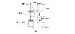
図8に示す半導体装置は、実施の形態2で示すトランジスタ750と同様な構造を適用することができるトランジスタ160、実施の形態1で示すトランジスタ410a、410b、410cと同様な構造を適用することができるトランジスタ162を有する。
The semiconductor device illustrated in FIG. 8 can have a structure similar to that of the
ここで、シリコン半導体などを用いたトランジスタ750と同様な構造を適用するトランジスタ160は、高速動作が容易である。一方で、酸化物半導体を用いた実施の形態1で示すトランジスタ410a、410b、410cと同様な構造を適用することができるトランジスタ162は、その特性により長時間の電荷保持を可能とする。
Here, the
なお、上記トランジスタは、いずれもnチャネル型トランジスタであるものとして説明するが、pチャネル型トランジスタを用いることができるのはいうまでもない。 Note that although all the above transistors are described as n-channel transistors, it goes without saying that p-channel transistors can be used.
図8において、第1の配線(1st Line)とトランジスタ160のソース電極層とは、電気的に接続され、第2の配線(2nd Line)とトランジスタ160のドレイン電極層とは、電気的に接続されている。また、第3の配線(3rd Line)とトランジスタ162のソース電極層又はドレイン電極層の一方とは、電気的に接続され、第4の配線(4th Line)と、トランジスタ162のゲート電極層とは、電気的に接続されている。そして、トランジスタ160のゲート電極層と、トランジスタ162のソース電極層又はドレイン電極層の他方は、容量素子164の電極の一方と電気的に接続され、第5の配線(5th Line)と、容量素子164の電極の他方は電気的に接続されている。
In FIG. 8, the first wiring (1st Line) and the source electrode layer of the
図8に示す半導体装置では、トランジスタ160のゲート電極層の電位が保持可能という特徴を生かすことで、次のように、情報の書き込み、保持、読み出しが可能である。
In the semiconductor device illustrated in FIG. 8, by using the feature that the potential of the gate electrode layer of the
情報の書き込みおよび保持について説明する。まず、第4の配線の電位を、トランジスタ162がオン状態となる電位にして、トランジスタ162をオン状態とする。これにより、第3の配線の電位が、トランジスタ160のゲート電極層、および容量素子164に与えられる。すなわち、トランジスタ160のゲート電極層には、所定の電荷が与えられる(書き込み)。ここでは、異なる二つの電位レベルを与える電荷(以下Lowレベル電荷、Highレベル電荷という)のいずれかが与えられるものとする。その後、第4の配線の電位を、トランジスタ162がオフ状態となる電位にして、トランジスタ162をオフ状態とすることにより、トランジスタ160のゲート電極層に与えられた電荷が保持される(保持)。
Information writing and holding will be described. First, the potential of the fourth wiring is set to a potential at which the
トランジスタ162のオフ電流は極めて小さいため、トランジスタ160のゲート電極層の電荷は長時間にわたって保持される。
Since the off-state current of the
次に情報の読み出しについて説明する。第1の配線に所定の電位(定電位)を与えた状態で、第5の配線に適切な電位(読み出し電位)を与えると、トランジスタ160のゲート電極層に保持された電荷量に応じて、第2の配線は異なる電位をとる。一般に、トランジスタ160をnチャネル型とすると、トランジスタ160のゲート電極層にHighレベル電荷が与えられている場合の見かけのしきい値Vth_Hは、トランジスタ160のゲート電極層にLowレベル電荷が与えられている場合の見かけのしきい値Vth_Lより低くなるためである。ここで、見かけのしきい値電圧とは、トランジスタ160を「オン状態」とするために必要な第5の配線の電位をいうものとする。したがって、第5の配線の電位をVth_HとVth_Lの間の電位V0とすることにより、トランジスタ160のゲート電極層に与えられた電荷を判別できる。例えば、書き込みにおいて、Highレベル電荷が与えられていた場合には、第5の配線の電位がV0(>Vth_H)となれば、トランジスタ160は「オン状態」となる。Lowレベル電荷が与えられていた場合には、第5の配線の電位がV0(<Vth_L)となっても、トランジスタ160は「オフ状態」のままである。このため、第2の配線の電位を見ることで、保持されている情報を読み出すことができる。
Next, reading of information will be described. When an appropriate potential (reading potential) is applied to the fifth wiring in a state where a predetermined potential (constant potential) is applied to the first wiring, according to the amount of charge held in the gate electrode layer of the
なお、メモリセルをアレイ状に配置して用いる場合、所望のメモリセルの情報のみを読み出せることが必要になる。このように情報を読み出さない場合には、ゲート電極層の状態にかかわらずトランジスタ160が「オフ状態」となるような電位、つまり、Vth_Hより小さい電位を第5の配線に与えればよい。又は、ゲート電極層の状態にかかわらずトランジスタ160が「オン状態」となるような電位、つまり、Vth_Lより大きい電位を第5の配線に与えればよい。
Note that in the case of using memory cells arranged in an array, it is necessary to read only information of a desired memory cell. In the case where information is not read out in this manner, a potential at which the
図9に異なる記憶装置の構造の一形態の例を示す。 FIG. 9 shows an example of one mode of a structure of a different storage device.
図9は、記憶装置の斜視図である。図9に示す記憶装置は上部に記憶回路としてメモリセルを複数含む、メモリセルアレイ(メモリセルアレイ3400(1)乃至メモリセルアレイ3400(n)nは2以上の整数)を複数層有し、下部にメモリセルアレイ3400(1)乃至メモリセルアレイ3400(n)を動作させるために必要な論理回路3004を有する。
FIG. 9 is a perspective view of the storage device. The memory device illustrated in FIG. 9 includes a plurality of memory cell arrays (memory cell array 3400 (1) to memory cell array 3400 (n) n are integers of 2 or more) including a plurality of memory cells as memory circuits in the upper portion, and a memory in the lower portion. A
図9では、論理回路3004、メモリセルアレイ3400(1)及びメモリセルアレイ3400(2)を図示しており、メモリセルアレイ3400(1)又はメモリセルアレイ3400(2)に含まれる複数のメモリセルのうち、メモリセル3170aと、メモリセル3170bを代表で示す。メモリセル3170a及びメモリセル3170bとしては、例えば、本実施の形態において説明した図8の回路構成と同様の構成とすることができる。
FIG. 9 illustrates a
なお、メモリセル3170a及びメモリセル3170bに含まれるトランジスタは、酸化物半導体膜にチャネル形成領域を有するトランジスタを用いる。酸化物半導体膜にチャネル形成領域を有するトランジスタの構成については、実施の形態1において説明した構成と同様であるため、説明は省略する。
Note that as the transistor included in the
また、論理回路3004は、酸化物半導体以外の半導体材料をチャネル形成領域として用いたトランジスタを有する。例えば、半導体材料(例えば、シリコンなど)を含む基板に素子分離絶縁層を設け、素子分離絶縁層に囲まれた領域にチャネル形成領域となる領域を形成することによって得られるトランジスタとすることができる。なお、トランジスタは、絶縁表面上に形成された多結晶シリコン膜等の半導体膜や、SOI基板のシリコン膜にチャネル形成領域が形成されるトランジスタであってもよい。
The
メモリセルアレイ3400(1)乃至メモリセルアレイ3400(n)及び論理回路3004は層間絶縁層を間に介して積層され、層間絶縁層を貫通する電極や配線によって適宜電気的接続等を行うことができる。
The memory cell arrays 3400 (1) to 3400 (n) and the
本実施の形態に示す半導体装置では、チャネル形成領域に酸化物半導体を用いたオフ電流の極めて小さいトランジスタを適用することで、極めて長期にわたり記憶内容を保持することが可能である。つまり、リフレッシュ動作が不要となるか、又は、リフレッシュ動作の頻度を極めて低くすることが可能となるため、消費電力を十分に低減することができる。また、電力の供給がない場合(ただし、電位は固定されていることが望ましい)であっても、長期にわたって記憶内容を保持することが可能である。 In the semiconductor device described in this embodiment, stored data can be held for an extremely long time by using a transistor with an extremely small off-state current that uses an oxide semiconductor for a channel formation region. In other words, the refresh operation becomes unnecessary or the frequency of the refresh operation can be made extremely low, so that power consumption can be sufficiently reduced. In addition, stored data can be held for a long time even when power is not supplied (note that a potential is preferably fixed).
また、本実施の形態に示す半導体装置では、情報の書き込みに高い電圧を必要とせず、素子の劣化の問題もない。例えば、従来の不揮発性メモリのように、フローティングゲートへの電子の注入や、フローティングゲートからの電子の引き抜きを行う必要がないため、ゲート絶縁膜の劣化といった問題が全く生じない。すなわち、開示する発明に係る半導体装置では、従来の不揮発性メモリで問題となっている書き換え可能回数に制限はなく、信頼性が飛躍的に向上する。さらに、トランジスタのオン状態、オフ状態によって、情報の書き込みが行われるため、高速な動作も容易に実現しうる。 In addition, in the semiconductor device described in this embodiment, high voltage is not needed for writing data and there is no problem of deterioration of elements. For example, unlike the conventional nonvolatile memory, it is not necessary to inject electrons into the floating gate or extract electrons from the floating gate, so that there is no problem of deterioration of the gate insulating film. That is, in the semiconductor device according to the disclosed invention, the number of rewritable times that is a problem in the conventional nonvolatile memory is not limited, and the reliability is dramatically improved. Further, since data is written depending on the on / off state of the transistor, high-speed operation can be easily realized.
以上のように、微細化及び高集積化を実現し、かつ高い電気的特性を付与された半導体装置、及び該半導体装置の作製方法を提供することができる。 As described above, a semiconductor device which is miniaturized and highly integrated and has high electrical characteristics, and a method for manufacturing the semiconductor device can be provided.
以上、本実施の形態に示す構成、方法などは、他の実施の形態に示す構成、方法などと適宜組み合わせて用いることができる。 The structures, methods, and the like described in this embodiment can be combined as appropriate with any of the structures, methods, and the like described in the other embodiments.
(実施の形態4)
本実施の形態では、半導体装置の一例として、上記実施の形態1に開示したトランジスタを少なくとも一部に用いたCPU(Central Processing Unit)について説明する。
(Embodiment 4)
In this embodiment, a CPU (Central Processing Unit) using at least part of the transistor disclosed in
図10(A)は、CPUの具体的な構成を示すブロック図である。図10(A)に示すCPUは、基板1190上に、ALU1191(ALU:Arithmetic logic unit、演算回路)、ALUコントローラ1192、インストラクションデコーダ1193、インタラプトコントローラ1194、タイミングコントローラ1195、レジスタ1196、レジスタコントローラ1197、バスインターフェース1198(Bus I/F)、書き換え可能なROM1199、及びROMインターフェース1189(ROM I/F)を有している。基板1190は、半導体基板、SOI基板、ガラス基板などを用いる。ROM1199及びROMインターフェース1189は、別チップに設けてもよい。もちろん、図10(A)に示すCPUは、その構成を簡略化して示した一例にすぎず、実際のCPUはその用途によって多種多様な構成を有している。
FIG. 10A is a block diagram illustrating a specific structure of a CPU. 10A, an ALU 1191 (ALU: Arithmetic logic unit, arithmetic circuit), an
バスインターフェース1198を介してCPUに入力された命令は、インストラクションデコーダ1193に入力され、デコードされた後、ALUコントローラ1192、インタラプトコントローラ1194、レジスタコントローラ1197、タイミングコントローラ1195に入力される。
Instructions input to the CPU via the
ALUコントローラ1192、インタラプトコントローラ1194、レジスタコントローラ1197、タイミングコントローラ1195は、デコードされた命令に基づき、各種制御を行なう。具体的にALUコントローラ1192は、ALU1191の動作を制御するための信号を生成する。また、インタラプトコントローラ1194は、CPUのプログラム実行中に、外部の入出力装置や、周辺回路からの割り込み要求を、その優先度やマスク状態から判断し、処理する。レジスタコントローラ1197は、レジスタ1196のアドレスを生成し、CPUの状態に応じてレジスタ1196の読み出しや書き込みを行なう。
The
また、タイミングコントローラ1195は、ALU1191、ALUコントローラ1192、インストラクションデコーダ1193、インタラプトコントローラ1194、及びレジスタコントローラ1197の動作のタイミングを制御する信号を生成する。例えばタイミングコントローラ1195は、基準クロック信号CLK1を元に、内部クロック信号CLK2を生成する内部クロック生成部を備えており、内部クロック信号CLK2を上記各種回路に供給する。
In addition, the
図10(A)に示すCPUでは、レジスタ1196に、メモリセルが設けられている。レジスタ1196のメモリセルには、上記実施の形態3に開示したメモリセルを用いることができる。
In the CPU illustrated in FIG. 10A, a memory cell is provided in the
図10(A)に示すCPUにおいて、レジスタコントローラ1197は、ALU1191からの指示に従い、レジスタ1196における保持動作の選択を行う。すなわち、レジスタ1196が有するメモリセルにおいて、論理(値)を反転させる論理素子によるデータの保持を行うか、容量素子によるデータの保持を行うかを、選択する。論理(値)を反転させる論理素子によるデータの保持が選択されている場合、レジスタ1196内のメモリセルへの、電源電圧の供給が行われる。容量素子におけるデータの保持が選択されている場合、容量素子へのデータの書き換えが行われ、レジスタ1196内のメモリセルへの電源電圧の供給を停止することができる。
In the CPU illustrated in FIG. 10A, the
電源停止に関しては、図10(B)または図10(C)に示すように、メモリセル群と、電源電位VDDまたは電源電位VSSの与えられているノード間に、スイッチング素子を設けることにより行うことができる。以下に図10(B)及び図10(C)の回路の説明を行う。 The power supply is stopped by providing a switching element between the memory cell group and a node to which the power supply potential VDD or the power supply potential VSS is applied as shown in FIG. 10B or 10C. Can do. The circuits in FIGS. 10B and 10C will be described below.
図10(B)及び図10(C)では、メモリセルへの電源電位の供給を制御するスイッチング素子に、上記実施の形態1に開示したトランジスタを含む記憶回路の構成の一例を示す。
10B and 10C illustrate an example of a structure of a memory circuit including the transistor disclosed in
図10(B)に示す記憶装置は、スイッチング素子1141と、メモリセル1142を複数有するメモリセル群1143とを有している。具体的に、各メモリセル1142には、実施の形態3に記載されているメモリセルを用いることができる。メモリセル群1143が有する各メモリセル1142には、スイッチング素子1141を介して、ハイレベルの電源電位VDDが供給されている。さらに、メモリセル群1143が有する各メモリセル1142には、信号INの電位と、ローレベルの電源電位VSSの電位が与えられている。
A memory device illustrated in FIG. 10B includes a
図10(B)では、スイッチング素子1141として、上記実施の形態1に開示したトランジスタを用いており、該トランジスタは、そのゲート電極層に与えられる信号SigAによりスイッチングが制御される。
In FIG. 10B, the transistor disclosed in
なお、図10(B)では、スイッチング素子1141がトランジスタを一つだけ有する構成を示しているが、特に限定されず、トランジスタを複数有していてもよい。スイッチング素子1141が、スイッチング素子として機能するトランジスタを複数有している場合、上記複数のトランジスタは並列に接続されていてもよいし、直列に接続されていてもよいし、直列と並列が組み合わされて接続されていてもよい。
Note that FIG. 10B illustrates a structure in which the
また、図10(B)では、スイッチング素子1141により、メモリセル群1143が有する各メモリセル1142への、ハイレベルの電源電位VDDの供給が制御されているが、スイッチング素子1141により、ローレベルの電源電位VSSの供給が制御されていてもよい。
In FIG. 10B, the
また、図10(C)には、メモリセル群1143が有する各メモリセル1142に、スイッチング素子1141を介して、ローレベルの電源電位VSSが供給されている、記憶装置の一例を示す。スイッチング素子1141により、メモリセル群1143が有する各メモリセル1142への、ローレベルの電源電位VSSの供給を制御することができる。
FIG. 10C illustrates an example of a memory device in which a low-level power supply potential VSS is supplied to each
メモリセル群と、電源電位VDDまたは電源電位VSSの与えられているノード間に、スイッチング素子を設け、一時的にCPUの動作を停止し、電源電圧の供給を停止した場合においてもデータを保持することが可能であり、消費電力の低減を行うことができる。具体的には、例えば、パーソナルコンピュータのユーザーが、キーボードなどの入力装置への情報の入力を停止している間でも、CPUの動作を停止することができ、それにより消費電力を低減することができる。 A switching element is provided between the memory cell group and a node to which the power supply potential VDD or the power supply potential VSS is applied to temporarily stop the operation of the CPU and retain data even when the supply of the power supply voltage is stopped. It is possible to reduce power consumption. Specifically, for example, the operation of the CPU can be stopped while the user of the personal computer stops inputting information to an input device such as a keyboard, thereby reducing power consumption. it can.
ここでは、CPUを例に挙げて説明したが、DSP(Digital Signal Processor)、カスタムLSI、FPGA(Field Programmable Gate Array)等のLSIにも応用可能である。 Here, the CPU has been described as an example, but the present invention can also be applied to LSIs such as a DSP (Digital Signal Processor), a custom LSI, and an FPGA (Field Programmable Gate Array).
以上、本実施の形態に示す構成、方法などは、他の実施の形態に示す構成、方法などと適宜組み合わせて用いることができる。 The structures, methods, and the like described in this embodiment can be combined as appropriate with any of the structures, methods, and the like described in the other embodiments.
(実施の形態5)
本明細書に開示する半導体装置は、さまざまな電子機器(遊技機も含む)に適用することができる。電子機器としては、テレビ、モニタ等の表示装置、照明装置、デスクトップ型或いはノート型のパーソナルコンピュータ、ワードプロセッサ、DVD(Digital Versatile Disc)などの記録媒体に記憶された静止画又は動画を再生する画像再生装置、ポータブルCDプレーヤ、ラジオ、テープレコーダ、ヘッドホンステレオ、ステレオ、コードレス電話子機、トランシーバ、携帯無線機、携帯電話、自動車電話、携帯型ゲーム機、電卓、携帯情報端末、電子手帳、電子書籍、電子翻訳機、音声入力機器、ビデオカメラ、デジタルスチルカメラ、電気シェーバ、電子レンジ等の高周波加熱装置、電気炊飯器、電気洗濯機、電気掃除機、エアコンディショナーなどの空調設備、食器洗い器、食器乾燥器、衣類乾燥器、布団乾燥器、電気冷蔵庫、電気冷凍庫、電気冷凍冷蔵庫、DNA保存用冷凍庫、煙感知器、放射線測定器、透析装置等の医療機器、などが挙げられる。さらに、誘導灯、信号機、ベルトコンベア、エレベータ、エスカレータ、産業用ロボット、電力貯蔵システム等の産業機器も挙げられる。また、石油を用いたエンジンや、非水系二次電池からの電力を用いて電動機により推進する移動体なども、電気機器の範疇に含まれるものとする。上記移動体として、例えば、電気自動車(EV)、内燃機関と電動機を併せ持ったハイブリッド車(HEV)、プラグインハイブリッド車(PHEV)、これらのタイヤ車輪を無限軌道に変えた装軌車両、電動アシスト自転車を含む原動機付自転車、自動二輪車、電動車椅子、ゴルフ用カート、小型又は大型船舶、潜水艦、ヘリコプター、航空機、ロケット、人工衛星、宇宙探査機や惑星探査機、宇宙船が挙げられる。これらの電子機器の具体例を図11乃至図13に示す。
(Embodiment 5)
The semiconductor device disclosed in this specification can be applied to a variety of electronic devices (including game machines). As electronic equipment, display devices such as televisions, monitors, lighting devices, desktop or notebook personal computers, word processors, image playback that plays back still images or moving images stored on recording media such as a DVD (Digital Versatile Disc) Device, Portable CD player, Radio, Tape recorder, Headphone stereo, Stereo, Cordless phone cordless handset, Transceiver, Portable radio, Mobile phone, Car phone, Portable game machine, Calculator, Personal digital assistant, Electronic notebook, Electronic book, Electronic translators, audio input devices, video cameras, digital still cameras, high-frequency heating devices such as electric shavers, microwave ovens, electric rice cookers, electric washing machines, vacuum cleaners, air conditioners, etc., dishwashers, dish drying Container, clothes dryer, futon dryer Vessels, electric refrigerators, electric freezers, electric refrigerator, DNA storage freezers, smoke detectors, radiation counters, medical devices such as dialyzers, and the like. Further examples include industrial equipment such as guide lights, traffic lights, belt conveyors, elevators, escalators, industrial robots, and power storage systems. In addition, an engine using petroleum, a moving body driven by an electric motor using electric power from a non-aqueous secondary battery, and the like are also included in the category of electric equipment. Examples of the moving body include an electric vehicle (EV), a hybrid vehicle (HEV) having both an internal combustion engine and an electric motor, a plug-in hybrid vehicle (PHEV), a tracked vehicle in which these tire wheels are changed to an endless track, and electric assist. Motorbikes including bicycles, motorcycles, electric wheelchairs, golf carts, small or large ships, submarines, helicopters, aircrafts, rockets, artificial satellites, space probes, planetary probes, and space ships. Specific examples of these electronic devices are illustrated in FIGS.
図11(A)は、表示部を有するテーブル9000を示している。テーブル9000は、筐体9001に表示部9003が組み込まれており、表示部9003により映像を表示することが可能である。なお、4本の脚部9002により筐体9001を支持した構成を示している。また、電力供給のための電源コード9005を筐体9001に有している。
FIG. 11A illustrates a table 9000 having a display portion. In the table 9000, a
実施の形態1に示すトランジスタは、表示部9003に用いることが可能であり、電子機器に高い信頼性を付与することができる。
The transistor described in
表示部9003は、タッチ入力機能を有しており、テーブル9000の表示部9003に表示された表示ボタン9004を指などで触れることで、画面操作や、情報を入力することができ、また他の家電製品との通信を可能とする、又は制御を可能とすることで、画面操作により他の家電製品をコントロールする制御装置としてもよい。例えば、イメージセンサ機能を有する半導体装置を用いれば、表示部9003にタッチ入力機能を持たせることができる。
The
また、筐体9001に設けられたヒンジによって、表示部9003の画面を床に対して垂直に立てることもでき、テレビジョン装置としても利用できる。狭い部屋においては、大きな画面のテレビジョン装置は設置すると自由な空間が狭くなってしまうが、テーブルに表示部が内蔵されていれば、部屋の空間を有効に利用することができる。
Further, the hinge of the
図11(B)は、携帯音楽プレーヤであり、本体3021には表示部3023と、耳に装着するための固定部3022と、スピーカ、操作ボタン3024、外部メモリスロット3025等が設けられている。実施の形態1乃至4のいずれか示したトランジスタ、メモリ、集積回路を本体3021に内蔵されているメモリやCPUなどに適用することにより、より省電力化された携帯音楽プレイヤー(PDA)とすることができる。
FIG. 11B shows a portable music player. A
さらに、図11(B)に示す携帯音楽プレーヤにアンテナやマイク機能や無線機能を持たせ、携帯電話と連携させれば、乗用車などを運転しながらワイヤレスによるハンズフリーでの会話も可能である。 Furthermore, if the portable music player shown in FIG. 11B has an antenna, a microphone function, and a wireless function and is linked to a mobile phone, a wireless hands-free conversation is possible while driving a passenger car or the like.
図11(C)はコンピュータであり、CPUを含む本体9201、筐体9202、表示部9203、キーボード9204、外部接続ポート9205、ポインティングデバイス9206等を含む。コンピュータは、本発明の一態様を用いて作製される半導体装置をその表示部9203に用いることにより作製される。実施の形態4に示したCPUを利用すれば、省電力化されたコンピュータとすることが可能となる。
FIG. 11C illustrates a computer, which includes a
図12(A)及び図12(B)は2つ折り可能なタブレット型端末である。図12(A)は、開いた状態であり、タブレット型端末は、筐体9630、表示部9631a、表示部9631b、表示モード切り替えスイッチ9034、電源スイッチ9035、省電力モード切り替えスイッチ9036、留め具9033、操作スイッチ9038、を有する。
12A and 12B illustrate a tablet terminal that can be folded. In FIG. FIG. 12A illustrates an open state in which the tablet terminal includes a
図12(A)及び図12(B)に示すような携帯機器においては、画像データの一時記憶などにメモリとしてSRAMまたはDRAMが使用されている。例えば、実施の形態3に説明した半導体装置をメモリとして使用することができる。先の実施の形態で説明した半導体装置をメモリに採用することによって、情報の書き込みおよび読み出しが高速で、長期間の記憶保持が可能で、且つ消費電力が十分に低減することができる。
In portable devices as shown in FIGS. 12A and 12B, SRAM or DRAM is used as a memory for temporary storage of image data. For example, the semiconductor device described in
また、表示部9631aは、一部をタッチパネルの領域9632aとすることができ、表示された操作キー9638にふれることでデータ入力をすることができる。なお、表示部9631aにおいては、一例として半分の領域が表示のみの機能を有する構成、もう半分の領域がタッチパネルの機能を有する構成を示しているが該構成に限定されない。表示部9631aの全ての領域がタッチパネルの機能を有する構成としても良い。例えば、表示部9631aの全面をキーボードボタン表示させてタッチパネルとし、表示部9631bを表示画面として用いることができる。
Part of the
また、表示部9631bにおいても表示部9631aと同様に、表示部9631bの一部をタッチパネルの領域9632bとすることができる。また、タッチパネルのキーボード表示切り替えボタン9639が表示されている位置に指やスタイラスなどでふれることで表示部9631bにキーボードボタン表示することができる。
Further, in the
また、タッチパネルの領域9632aとタッチパネルの領域9632bに対して同時にタッチ入力することもできる。
Touch input can be performed simultaneously on the
また、表示モード切り替えスイッチ9034は、縦表示又は横表示などの表示の向きを切り替え、白黒表示やカラー表示の切り替えなどを選択できる。省電力モード切り替えスイッチ9036は、タブレット型端末に内蔵している光センサで検出される使用時の外光の光量に応じて表示の輝度を最適なものとすることができる。タブレット型端末は光センサだけでなく、ジャイロ、加速度センサ等の傾きを検出するセンサなどの他の検出装置を内蔵させてもよい。
A display
また、図12(A)では表示部9631bと表示部9631aの表示面積が同じ例を示しているが特に限定されず、一方のサイズともう一方のサイズが異なっていてもよく、表示の品質も異なっていてもよい。例えば一方が他方よりも高精細な表示を行える表示パネルとしてもよい。
FIG. 12A illustrates an example in which the display areas of the
図12(B)は、閉じた状態であり、タブレット型端末は、筐体9630、太陽電池9633、充放電制御回路9634、バッテリー9635、DCDCコンバータ9636を有する。なお、図12(B)では充放電制御回路9634の一例としてバッテリー9635、DCDCコンバータ9636を有する構成について示している。
FIG. 12B illustrates a closed state, in which the tablet terminal includes a
なお、タブレット型端末は2つ折り可能なため、未使用時に筐体9630を閉じた状態にすることができる。従って、表示部9631a、表示部9631bを保護できるため、耐久性に優れ、長期使用の観点からも信頼性の優れたタブレット型端末を提供できる。
Note that since the tablet terminal can be folded in two, the
また、この他にも図12(A)及び図12(B)に示したタブレット型端末は、様々な情報(静止画、動画、テキスト画像など)を表示する機能、カレンダー、日付又は時刻などを表示部に表示する機能、表示部に表示した情報をタッチ入力操作又は編集するタッチ入力機能、様々なソフトウェア(プログラム)によって処理を制御する機能、等を有することができる。 In addition, the tablet terminal shown in FIGS. 12A and 12B has a function for displaying various information (still images, moving images, text images, etc.), a calendar, a date, or a time. A function for displaying on the display unit, a touch input function for performing touch input operation or editing of information displayed on the display unit, a function for controlling processing by various software (programs), and the like can be provided.
タブレット型端末の表面に装着された太陽電池9633によって、電力をタッチパネル、表示部、又は映像信号処理部等に供給することができる。なお、太陽電池9633は、筐体9630の片面又は両面に設けることができ、バッテリー9635の充電を効率的に行う構成とすることができる。なおバッテリー9635としては、リチウムイオン電池を用いると、小型化を図れる等の利点がある。
Electric power can be supplied to the touch panel, the display unit, the video signal processing unit, or the like by the
また、図12(B)に示す充放電制御回路9634の構成、及び動作について図12(C)にブロック図を示し説明する。図12(C)には、太陽電池9633、バッテリー9635、DCDCコンバータ9636、コンバータ9637、スイッチSW1乃至SW3、表示部9631について示しており、バッテリー9635、DCDCコンバータ9636、コンバータ9637、スイッチSW1乃至SW3が、図12(B)に示す充放電制御回路9634に対応する箇所となる。
The structure and operation of the charge /
まず外光により太陽電池9633により発電がされる場合の動作の例について説明する。太陽電池9633で発電した電力は、バッテリー9635を充電するための電圧となるようDCDCコンバータ9636で昇圧又は降圧がなされる。そして、表示部9631の動作に太陽電池9633からの電力が用いられる際にはスイッチSW1をオンにし、コンバータ9637で表示部9631に必要な電圧に昇圧又は降圧をすることとなる。また、表示部9631での表示を行わない際には、SW1をオフにし、SW2をオンにしてバッテリー9635の充電を行う構成とすればよい。
First, an example of operation in the case where power is generated by the
なお太陽電池9633については、発電手段の一例として示したが、特に限定されず、圧電素子(ピエゾ素子)や熱電変換素子(ペルティエ素子)などの他の発電手段によるバッテリー9635の充電を行う構成であってもよい。例えば、無線(非接触)で電力を送受信して充電する無接点電力伝送モジュールや、また他の充電手段を組み合わせて行う構成としてもよい。
Note that the
図13(A)において、テレビジョン装置8000は、筐体8001に表示部8002が組み込まれており、表示部8002により映像を表示し、スピーカ部8003から音声を出力することが可能である。実施の形態1に示すトランジスタを用いて表示部8002に用いることが可能である。
In FIG. 13A, a
表示部8002は、液晶表示装置、有機EL素子などの発光素子を各画素に備えた発光装置、電気泳動表示装置、DMD(Digital Micromirror Device)、PDP(Plasma Display Panel)などの、半導体表示装置を用いることができる。
The
テレビジョン装置8000は、受信機やモデムなどを備えていてもよい。テレビジョン装置8000は、受信機により一般のテレビ放送の受信を行うことができ、さらにモデムを介して有線又は無線による通信ネットワークに接続することにより、一方向(送信者から受信者)又は双方向(送信者と受信者間、あるいは受信者間同士など)の情報通信を行うことも可能である。
The
また、テレビジョン装置8000は、情報通信を行うためのCPUや、メモリを備えていてもよい。テレビジョン装置8000は、実施の形態2乃至4のいずれかに示す集積回路、メモリ、又はCPUを用いることが可能である。
In addition, the
図13(A)において、室内機8200及び室外機8204を有するエアコンディショナーは、実施の形態4のCPUを用いた電気機器の一例である。具体的に、室内機8200は、筐体8201、送風口8202、CPU8203等を有する。図13(A)において、CPU8203が、室内機8200に設けられている場合を例示しているが、CPU8203は室外機8204に設けられていてもよい。或いは、室内機8200と室外機8204の両方に、CPU8203が設けられていてもよい。実施の形態4に示したCPUは、酸化物半導体を用いたCPUであるため、耐熱性に優れており、信頼性の高いエアコンディショナーを実現できる。
In FIG. 13A, an air conditioner including an
図13(A)において、電気冷凍冷蔵庫8300は、酸化物半導体を用いたCPUを備える電気機器の一例である。具体的に、電気冷凍冷蔵庫8300は、筐体8301、冷蔵室用扉8302、冷凍室用扉8303、CPU8304等を有する。図13(A)では、CPU8304が、筐体8301の内部に設けられている。実施の形態4に示したCPUを電気冷凍冷蔵庫8300のCPU8304に用いることによって省電力化が図れる。
In FIG. 13A, an electric refrigerator-
図13(B)及び図13(C)において、電気機器の一例である電気自動車の例を示す。電気自動車9700には、二次電池9701が搭載されている。二次電池9701の電力は、制御回路9702により出力が調整されて、駆動装置9703に供給される。制御回路9702は、図示しないROM、RAM、CPU等を有する処理装置9704によって制御される。実施の形態4に示したCPUを電気自動車9700のCPUに用いることによって省電力化が図れる。
FIG. 13B and FIG. 13C illustrate an example of an electric vehicle which is an example of an electric device. An
駆動装置9703は、直流電動機若しくは交流電動機単体、又は電動機と内燃機関と、を組み合わせて構成される。処理装置9704は、電気自動車9700の運転者の操作情報(加速、減速、停止など)や走行時の情報(上り坂や下り坂等の情報、駆動輪にかかる負荷情報など)の入力情報に基づき、制御回路9702に制御信号を出力する。制御回路9702は、処理装置9704の制御信号により、二次電池9701から供給される電気エネルギーを調整して駆動装置9703の出力を制御する。交流電動機を搭載している場合は、図示していないが、直流を交流に変換するインバータも内蔵される。
The
以上、本実施の形態に示す構成、方法などは、他の実施の形態に示す構成、方法などと適宜組み合わせて用いることができる。 The structures, methods, and the like described in this embodiment can be combined as appropriate with any of the structures, methods, and the like described in the other embodiments.
本実施例では、本明細書に開示する半導体装置に用いるインジウム、ガリウム、及び亜鉛を主成分として含む酸化物半導体膜、及びインジウム、ガリウム、亜鉛、及び窒素を主成分として含む酸化物膜のエッチング特性の評価を行った。 In this embodiment, an oxide semiconductor film containing indium, gallium, and zinc as main components and an oxide film containing indium, gallium, zinc, and nitrogen as main components used for the semiconductor device disclosed in this specification is etched. The characteristics were evaluated.
ガラス基板上に、インジウム、ガリウム、及び亜鉛を主成分として含む酸化物半導体膜として、In:Ga:Zn=1:1:1[原子数比]の酸化物ターゲットを用いたスパッタリング法により、膜厚500nmのIGZO膜を形成した。成膜条件は、アルゴン及び酸素(アルゴン:酸素=30sccm:15sccm)雰囲気下、圧力0.4Pa、電源電力0.5kW、基板とターゲットとの距離60mmとした。なお、成膜時の基板温度を2条件とし、200℃のIGZO膜と、400℃のIGZO膜2種類作製した。 A film formed on a glass substrate by a sputtering method using an oxide target of In: Ga: Zn = 1: 1: 1 [atomic ratio] as an oxide semiconductor film containing indium, gallium, and zinc as main components. An IGZO film having a thickness of 500 nm was formed. The deposition conditions were argon and oxygen (argon: oxygen = 30 sccm: 15 sccm), a pressure of 0.4 Pa, a power supply power of 0.5 kW, and a distance between the substrate and the target of 60 mm. The substrate temperature during film formation was two conditions, and two types of IGZO films of 200 ° C. and 400 ° C. were produced.
ガラス基板上に、インジウム、ガリウム、亜鉛、及び窒素を主成分として含む酸化物膜として、In:Ga:Zn=1:1:1[原子数比]の酸化物ターゲットを用いたスパッタリング法により、膜厚100nmのIGZON膜を形成した。成膜条件は、窒素(窒素=40sccm)雰囲気下、圧力0.4Pa、電源電力0.5kW、基板とターゲットとの距離60mmとした。なお、成膜時の基板温度を2条件とし、200℃のIGZON膜と、400℃のIGZON膜2種類作製した。 A sputtering method using an oxide target of In: Ga: Zn = 1: 1: 1 [atomic ratio] as an oxide film containing indium, gallium, zinc, and nitrogen as main components over a glass substrate, An IGZON film having a thickness of 100 nm was formed. The film formation conditions were a nitrogen (nitrogen = 40 sccm) atmosphere, a pressure of 0.4 Pa, a power supply power of 0.5 kW, and a distance between the substrate and the target of 60 mm. The substrate temperature during film formation was two conditions, and two types of IGZON films at 200 ° C. and IGZON films at 400 ° C. were produced.
4種類のIGZO膜及びIGZON膜にそれぞれ、燐酸と酢酸と硝酸との混合液(混酸アルミ液(2.0重量%の硝酸と、9.8重量%の酢酸と、72.3重量%のリン酸と、を含有する水溶液)和光純薬工業株式会社製)を用いて、室温にてエッチング工程を行い、エッチングレートを評価した。図14(A)に、4種類のIGZO膜(菱形のドット)及びIGZON膜(四角形のドット)のエッチングレートを示す。なお、図14(A)において、横軸は成膜時基板温度(℃)、縦軸はエッチングレート(nm/min)である。成膜時基板温度200℃のIGZO膜のエッチングレートは約67nm/min、成膜時基板温度400℃のIGZO膜のエッチングレートは約28nm/min、成膜時基板温度200℃のIGZON膜のエッチングレートは約2nm/min、成膜時基板温度400℃のIGZON膜のエッチングレートは約1nm/minであり、成膜時温度にかかわらず、IGZON膜のエッチングレートの方がIGZO膜のエッチングレートより低かった。 A mixture of phosphoric acid, acetic acid and nitric acid (a mixed acid aluminum solution (2.0% by weight nitric acid, 9.8% by weight acetic acid and 72.3% by weight phosphorus) was added to each of the four types of IGZO film and IGZON film. Using an aqueous solution containing acid) manufactured by Wako Pure Chemical Industries, Ltd., an etching process was performed at room temperature to evaluate the etching rate. FIG. 14A shows etching rates of four types of IGZO films (diamond dots) and IGZON films (square dots). In FIG. 14A, the horizontal axis represents the substrate temperature during film formation (° C.), and the vertical axis represents the etching rate (nm / min). The etching rate of the IGZO film having a substrate temperature of 200 ° C. during deposition is approximately 67 nm / min, the etching rate of the IGZO film having a substrate temperature of 400 ° C. during deposition is approximately 28 nm / min, and the etching of the IGZO film having a substrate temperature of 200 ° C. during deposition. The etching rate of the IGZON film with a rate of about 2 nm / min and the substrate temperature of 400 ° C. during film formation is about 1 nm / min. It was low.
図14(A)のエッチングレートより、成膜時基板温度が同じIGZO膜とIGZON膜において、エッチングレート選択比(IGZO膜のエッチングレート/IGZON膜のエッチングレート)を算出した。図14(B)にエッチングレート選択比を示す。なお、図14(B)において、横軸は成膜時基板温度(℃)、縦軸はエッチングレート選択比である。
成膜時基板温度200℃におけるエッチングレート選択比は約30、成膜時基板温度400℃におけるエッチングレート選択比は約20であり、いずれにおいてもエッチングレート選択比20以上という高いエッチングレート選択比が得られたことが確認できた。
From the etching rate in FIG. 14A, the etching rate selectivity (IGZO film etching rate / IGZON film etching rate) was calculated for the IGZO film and the IGZON film having the same substrate temperature during film formation. FIG. 14B shows the etching rate selection ratio. In FIG. 14B, the horizontal axis represents the substrate temperature during deposition (° C.) and the vertical axis represents the etching rate selection ratio.
The etching rate selection ratio at a substrate temperature of 200 ° C. during film formation is about 30, and the etching rate selection ratio at a substrate temperature of 400 ° C. during film formation is about 20. It was confirmed that it was obtained.
このように、インジウム、ガリウム、及び亜鉛を主成分として含む酸化物半導体膜(IGZO膜)と、インジウム、ガリウム、亜鉛、及び窒素を主成分として含む酸化物膜(IGZON膜)は、燐酸と酢酸と硝酸との混合液を用いたエッチング工程において、選択比を有するので、該選択比を用いて微細加工が可能となり、インジウム、ガリウム、及び亜鉛を主成分として含む酸化物半導体膜(IGZO膜)及びインジウム、ガリウム、亜鉛、及び窒素を主成分として含む酸化物膜(IGZON膜)の細幅な柱状体を作製することができる。よって、該細幅な柱状体を含む微細なトランジスタを用いることで、半導体装置の高集積化が可能となる。 As described above, an oxide semiconductor film (IGZO film) containing indium, gallium, and zinc as main components and an oxide film (IGZON film) containing indium, gallium, zinc, and nitrogen as main components are phosphoric acid and acetic acid. The etching process using a mixed solution of nitric acid and nitric acid has a selectivity, so that fine processing is possible using the selectivity, and an oxide semiconductor film (IGZO film) containing indium, gallium, and zinc as main components In addition, a narrow columnar body of an oxide film (IGZON film) containing indium, gallium, zinc, and nitrogen as main components can be manufactured. Therefore, high integration of a semiconductor device can be achieved by using a fine transistor including the narrow columnar body.
Claims (7)
前記第1の電極層上に第1の酸化物膜を形成し、
前記第1の酸化物膜上に酸化物半導体膜を形成し、
前記酸化物半導体膜上に第2の酸化物膜を形成し、
前記第2の酸化物膜を線幅方向に後退させながらマスクとして用いて、前記酸化物半導体膜をエッチングし、前記酸化物半導体膜及び前記第2の酸化物膜の柱状体を形成し、
前記柱状体上に絶縁膜を形成し、
前記絶縁膜上に島状の導電膜を形成し、
前記絶縁膜及び前記島状の導電膜を異方性エッチングして、前記柱状体における前記酸化物半導体膜の側面を覆うゲート絶縁膜と、前記ゲート絶縁膜を介して前記柱状体における前記酸化物半導体膜と重なり、かつ対向する第1のゲート電極層及び第2のゲート電極層とを形成し、
前記柱状体における前記第2の酸化物膜に電気的に接続する第2の電極層を形成することを特徴とする半導体装置の作製方法。 Forming a first electrode layer;
A first oxide film formed on the first electrode layer,
Forming an oxide semiconductor film on the first oxide film;
Forming a second oxide film on the oxide semiconductor film;
Used as a mask while retracting the second oxide film in a line width direction, the oxide semiconductor film was d etching, to form a columnar body before Symbol oxide semiconductor film and the second oxide film ,
Forming an insulating film on the columnar body;
Forming an island-shaped conductive film on the insulating film;
Wherein the insulating film and the island-shaped conductive film is anisotropically etched, a gate insulating film covering the contact Keru side surface of the oxide semiconductor film on the columnar body, the in the columnar body via the gate insulating film Forming a first gate electrode layer and a second gate electrode layer that overlap with and face the oxide semiconductor film;
A method for manufacturing a semiconductor device, comprising forming a second electrode layer electrically connected to the second oxide film in the columnar body.
前記第1の電極層、前記第1の酸化物膜、前記柱状体、前記ゲート絶縁膜、前記第1のゲート電極層、及び前記第2のゲート電極層上に層間絶縁膜を形成し、
前記層間絶縁膜を選択的に除去して前記柱状体における前記第2の酸化物膜を露出し、
前記露出した第2の酸化物膜と接して前記第2の電極層を形成することを特徴とする半導体装置の作製方法。 In claim 1,
Forming an interlayer insulating film on the first electrode layer, the first oxide film, the columnar body, the gate insulating film, the first gate electrode layer, and the second gate electrode layer;
Selectively removing the interlayer insulating film to expose the second oxide film in the columnar body;
A method for manufacturing a semiconductor device, wherein the second electrode layer is formed in contact with the exposed second oxide film.
前記エッチングは、酢酸、硝酸、及び燐酸の混合液を用い、
前記第1の酸化物膜及び前記第2の酸化物膜は、前記酸化物半導体膜より、酢酸、硝酸、及び燐酸の混合液を用いた前記エッチングに対して耐性があり、該エッチングの速度が遅いことを特徴とする半導体装置の作製方法。 In claim 1 or claim 2,
The etching uses a mixed solution of acetic acid, nitric acid, and phosphoric acid,
The first oxide film and the second oxide film, than the oxide semiconductor film, acetic acid, nitric acid, and has the resistance to the etching liquid mixture with phosphoric acid, the speed of the etching A method for manufacturing a semiconductor device, which is slow.
前記第1の酸化物膜及び前記第2の酸化物膜は、前記酸化物半導体膜より低抵抗であり、
前記酸化物半導体膜はチャネル形成領域として機能し、
前記第1の酸化物膜及び前記第2の酸化物膜は、ソース領域又はドレイン領域として機能することを特徴とする半導体装置の作製方法。 In any one of Claims 1 thru | or 3,
The first oxide film and the second oxide film have a lower resistance than the oxide semiconductor film,
The oxide semiconductor film functions as a channel formation region,
The method for manufacturing a semiconductor device, wherein the first oxide film and the second oxide film function as a source region or a drain region.
前記エッチングする前に、前記酸化物半導体膜及び前記第2の酸化物膜上にレジストマスクを形成し、前記レジストマスクを用いた異方性エッチングにより前記酸化物半導体膜、及び前記第2の酸化物膜を島状に加工することを特徴とする半導体装置の作製方法。 In any one of Claims 1 thru | or 4,
Before the etching, the oxide semiconductor film and a resist mask is formed on the second oxide film, the resist mask more the oxide semiconductor film to anisotropic etching grayed with, and the second A method for manufacturing a semiconductor device, wherein the oxide film is processed into an island shape.
前記第2の酸化物膜は、インジウム、ガリウム、亜鉛、及び窒素を主成分として含むターゲットを用いたスパッタリング法により形成することを特徴とする半導体装置の作製方法。 In any one of Claims 1 thru | or 5,
The method for manufacturing a semiconductor device is characterized in that the second oxide film is formed by a sputtering method using a target containing indium, gallium, zinc, and nitrogen as main components.
前記第2の酸化物膜は、インジウム、ガリウム、亜鉛を主成分として含む酸化物膜を形成し、該酸化物膜に窒素を導入して形成することを特徴とする半導体装置の作製方法。 In any one of Claims 1 thru | or 5,
The method for manufacturing a semiconductor device is characterized in that the second oxide film is formed by forming an oxide film containing indium, gallium, and zinc as main components and introducing nitrogen into the oxide film.
Priority Applications (1)
| Application Number | Priority Date | Filing Date | Title |
|---|---|---|---|
| JP2013089149A JP6100071B2 (en) | 2012-04-30 | 2013-04-22 | Method for manufacturing semiconductor device |
Applications Claiming Priority (3)
| Application Number | Priority Date | Filing Date | Title |
|---|---|---|---|
| JP2012104279 | 2012-04-30 | ||
| JP2012104279 | 2012-04-30 | ||
| JP2013089149A JP6100071B2 (en) | 2012-04-30 | 2013-04-22 | Method for manufacturing semiconductor device |
Publications (3)
| Publication Number | Publication Date |
|---|---|
| JP2013251533A JP2013251533A (en) | 2013-12-12 |
| JP2013251533A5 JP2013251533A5 (en) | 2016-05-19 |
| JP6100071B2 true JP6100071B2 (en) | 2017-03-22 |
Family
ID=49476514
Family Applications (1)
| Application Number | Title | Priority Date | Filing Date |
|---|---|---|---|
| JP2013089149A Expired - Fee Related JP6100071B2 (en) | 2012-04-30 | 2013-04-22 | Method for manufacturing semiconductor device |
Country Status (2)
| Country | Link |
|---|---|
| US (1) | US8772771B2 (en) |
| JP (1) | JP6100071B2 (en) |
Cited By (1)
| Publication number | Priority date | Publication date | Assignee | Title |
|---|---|---|---|---|
| US11074944B2 (en) | 2018-10-31 | 2021-07-27 | Toshiba Memory Corporation | Semiconductor memory device |
Families Citing this family (25)
| Publication number | Priority date | Publication date | Assignee | Title |
|---|---|---|---|---|
| US9368619B2 (en) | 2013-02-08 | 2016-06-14 | Taiwan Semiconductor Manufacturing Company, Ltd. | Method for inducing strain in vertical semiconductor columns |
| US9466668B2 (en) | 2013-02-08 | 2016-10-11 | Taiwan Semiconductor Manufacturing Company, Ltd. | Inducing localized strain in vertical nanowire transistors |
| US9209247B2 (en) | 2013-05-10 | 2015-12-08 | Taiwan Semiconductor Manufacturing Company, Ltd. | Self-aligned wrapped-around structure |
| US9978863B2 (en) * | 2013-08-16 | 2018-05-22 | Taiwan Semiconductor Manufacturing Company Limited | Semiconductor arrangement with one or more semiconductor columns |
| US9859439B2 (en) | 2013-09-18 | 2018-01-02 | Semiconductor Energy Laboratory Co., Ltd. | Semiconductor device and method for manufacturing the same |
| KR20160087024A (en) | 2015-01-12 | 2016-07-21 | 삼성디스플레이 주식회사 | Thin film transistor and method for fabricaing the same |
| US9564493B2 (en) | 2015-03-13 | 2017-02-07 | Taiwan Semiconductor Manufacturing Company, Ltd. | Devices having a semiconductor material that is semimetal in bulk and methods of forming the same |
| US10141232B2 (en) | 2016-06-30 | 2018-11-27 | International Business Machines Corporation | Vertical CMOS devices with common gate stacks |
| US10014305B2 (en) | 2016-11-01 | 2018-07-03 | Micron Technology, Inc. | Methods of forming an array comprising pairs of vertically opposed capacitors and arrays comprising pairs of vertically opposed capacitors |
| US10062745B2 (en) | 2017-01-09 | 2018-08-28 | Micron Technology, Inc. | Methods of forming an array of capacitors, methods of forming an array of memory cells individually comprising a capacitor and a transistor, arrays of capacitors, and arrays of memory cells individually comprising a capacitor and a transistor |
| US9935114B1 (en) | 2017-01-10 | 2018-04-03 | Micron Technology, Inc. | Methods of forming an array comprising pairs of vertically opposed capacitors and arrays comprising pairs of vertically opposed capacitors |
| US9842839B1 (en) * | 2017-01-12 | 2017-12-12 | Micron Technology, Inc. | Memory cell, an array of memory cells individually comprising a capacitor and a transistor with the array comprising rows of access lines and columns of digit lines, a 2T-1C memory cell, and methods of forming an array of capacitors and access transistors there-above |
| US10312239B2 (en) | 2017-03-16 | 2019-06-04 | Toshiba Memory Corporation | Semiconductor memory including semiconductor oxie |
| US10497712B2 (en) | 2017-03-16 | 2019-12-03 | Toshiba Memory Corporation | Semiconductor memory |
| TWI648825B (en) * | 2017-03-16 | 2019-01-21 | 日商東芝記憶體股份有限公司 | Semiconductor memory |
| US10553601B2 (en) | 2017-03-16 | 2020-02-04 | Toshiba Memory Corporation | Semiconductor memory including semiconductor oxide |
| US11380797B2 (en) | 2017-06-20 | 2022-07-05 | Intel Corporation | Thin film core-shell fin and nanowire transistors |
| JP7109928B2 (en) | 2018-01-31 | 2022-08-01 | キオクシア株式会社 | TRANSISTOR, SEMICONDUCTOR MEMORY DEVICE, AND TRANSISTOR MANUFACTURING METHOD |
| US10388658B1 (en) | 2018-04-27 | 2019-08-20 | Micron Technology, Inc. | Transistors, arrays of transistors, arrays of memory cells individually comprising a capacitor and an elevationally-extending transistor, and methods of forming an array of transistors |
| WO2020076758A1 (en) * | 2018-10-09 | 2020-04-16 | Micron Technology, Inc. | Devices including vertical transistors having hydrogen barrier materials, and related methods |
| WO2020076766A1 (en) * | 2018-10-09 | 2020-04-16 | Micron Technology, Inc. | Methods of forming a device, and related devices and electronic systems |
| EP3864704A4 (en) * | 2018-10-09 | 2022-10-12 | Micron Technology, Inc. | Devices and electronic systems including vertical transistors, and related methods |
| JP2021150525A (en) * | 2020-03-19 | 2021-09-27 | キオクシア株式会社 | Semiconductor storage device and manufacturing method for semiconductor storage device |
| CN111599870A (en) * | 2020-05-29 | 2020-08-28 | 京东方科技集团股份有限公司 | Thin film transistor switch, preparation method thereof, array substrate and display panel |
| US11430895B2 (en) * | 2020-06-03 | 2022-08-30 | Micron Technology, Inc. | Transistors including oxide semiconductive materials, and related microelectronic devices, memory devices, electronic systems, and methods |
Family Cites Families (107)
| Publication number | Priority date | Publication date | Assignee | Title |
|---|---|---|---|---|
| WO1997006554A2 (en) | 1995-08-03 | 1997-02-20 | Philips Electronics N.V. | Semiconductor device provided with transparent switching element |
| JP3625598B2 (en) | 1995-12-30 | 2005-03-02 | 三星電子株式会社 | Manufacturing method of liquid crystal display device |
| JP4170454B2 (en) | 1998-07-24 | 2008-10-22 | Hoya株式会社 | Article having transparent conductive oxide thin film and method for producing the same |
| JP2000150861A (en) | 1998-11-16 | 2000-05-30 | Tdk Corp | Oxide thin film |
| JP3276930B2 (en) | 1998-11-17 | 2002-04-22 | 科学技術振興事業団 | Transistor and semiconductor device |
| TW460731B (en) | 1999-09-03 | 2001-10-21 | Ind Tech Res Inst | Electrode structure and production method of wide viewing angle LCD |
| JP4089858B2 (en) | 2000-09-01 | 2008-05-28 | 国立大学法人東北大学 | Semiconductor device |
| KR20020038482A (en) | 2000-11-15 | 2002-05-23 | 모리시타 요이찌 | Thin film transistor array, method for producing the same, and display panel using the same |
| US6531727B2 (en) * | 2001-02-09 | 2003-03-11 | Micron Technology, Inc. | Open bit line DRAM with ultra thin body transistors |
| JP3997731B2 (en) | 2001-03-19 | 2007-10-24 | 富士ゼロックス株式会社 | Method for forming a crystalline semiconductor thin film on a substrate |
| JP2002289859A (en) | 2001-03-23 | 2002-10-04 | Minolta Co Ltd | Thin-film transistor |
| JP4090716B2 (en) | 2001-09-10 | 2008-05-28 | 雅司 川崎 | Thin film transistor and matrix display device |
| JP3925839B2 (en) | 2001-09-10 | 2007-06-06 | シャープ株式会社 | Semiconductor memory device and test method thereof |
| JP2003101012A (en) | 2001-09-25 | 2003-04-04 | Sony Corp | Semiconductor device and manufacturing method therefor |
| JP4164562B2 (en) | 2002-09-11 | 2008-10-15 | 独立行政法人科学技術振興機構 | Transparent thin film field effect transistor using homologous thin film as active layer |
| US7061014B2 (en) | 2001-11-05 | 2006-06-13 | Japan Science And Technology Agency | Natural-superlattice homologous single crystal thin film, method for preparation thereof, and device using said single crystal thin film |
| JP4083486B2 (en) | 2002-02-21 | 2008-04-30 | 独立行政法人科学技術振興機構 | Method for producing LnCuO (S, Se, Te) single crystal thin film |
| US7049190B2 (en) | 2002-03-15 | 2006-05-23 | Sanyo Electric Co., Ltd. | Method for forming ZnO film, method for forming ZnO semiconductor layer, method for fabricating semiconductor device, and semiconductor device |
| JP3933591B2 (en) | 2002-03-26 | 2007-06-20 | 淳二 城戸 | Organic electroluminescent device |
| US7339187B2 (en) | 2002-05-21 | 2008-03-04 | State Of Oregon Acting By And Through The Oregon State Board Of Higher Education On Behalf Of Oregon State University | Transistor structures |
| JP2004022625A (en) | 2002-06-13 | 2004-01-22 | Murata Mfg Co Ltd | Manufacturing method of semiconductor device and its manufacturing method |
| US7105868B2 (en) | 2002-06-24 | 2006-09-12 | Cermet, Inc. | High-electron mobility transistor with zinc oxide |
| WO2004021445A1 (en) * | 2002-08-28 | 2004-03-11 | National Institute Of Advanced Industrial Science And Technology | Double-gate type mos field effect transistor and production method therefor |
| US6632712B1 (en) * | 2002-10-03 | 2003-10-14 | Chartered Semiconductor Manufacturing Ltd. | Method of fabricating variable length vertical transistors |
| US7067843B2 (en) | 2002-10-11 | 2006-06-27 | E. I. Du Pont De Nemours And Company | Transparent oxide semiconductor thin film transistors |
| US7138685B2 (en) * | 2002-12-11 | 2006-11-21 | International Business Machines Corporation | Vertical MOSFET SRAM cell |
| JP4166105B2 (en) | 2003-03-06 | 2008-10-15 | シャープ株式会社 | Semiconductor device and manufacturing method thereof |
| JP2004273732A (en) | 2003-03-07 | 2004-09-30 | Sharp Corp | Active matrix substrate and its producing process |
| JP4108633B2 (en) | 2003-06-20 | 2008-06-25 | シャープ株式会社 | THIN FILM TRANSISTOR, MANUFACTURING METHOD THEREOF, AND ELECTRONIC DEVICE |
| US7262463B2 (en) | 2003-07-25 | 2007-08-28 | Hewlett-Packard Development Company, L.P. | Transistor including a deposited channel region having a doped portion |
| US7282782B2 (en) | 2004-03-12 | 2007-10-16 | Hewlett-Packard Development Company, L.P. | Combined binary oxide semiconductor device |
| US7145174B2 (en) | 2004-03-12 | 2006-12-05 | Hewlett-Packard Development Company, Lp. | Semiconductor device |
| EP2246894B2 (en) | 2004-03-12 | 2018-10-10 | Japan Science and Technology Agency | Method for fabricating a thin film transistor having an amorphous oxide as a channel layer |
| US7297977B2 (en) | 2004-03-12 | 2007-11-20 | Hewlett-Packard Development Company, L.P. | Semiconductor device |
| US7211825B2 (en) | 2004-06-14 | 2007-05-01 | Yi-Chi Shih | Indium oxide-based thin film transistors and circuits |
| JP2006100760A (en) | 2004-09-02 | 2006-04-13 | Casio Comput Co Ltd | Thin-film transistor and its manufacturing method |
| US7285501B2 (en) | 2004-09-17 | 2007-10-23 | Hewlett-Packard Development Company, L.P. | Method of forming a solution processed device |
| US7298084B2 (en) | 2004-11-02 | 2007-11-20 | 3M Innovative Properties Company | Methods and displays utilizing integrated zinc oxide row and column drivers in conjunction with organic light emitting diodes |
| US7863611B2 (en) | 2004-11-10 | 2011-01-04 | Canon Kabushiki Kaisha | Integrated circuits utilizing amorphous oxides |
| WO2006051994A2 (en) | 2004-11-10 | 2006-05-18 | Canon Kabushiki Kaisha | Light-emitting device |
| US7868326B2 (en) | 2004-11-10 | 2011-01-11 | Canon Kabushiki Kaisha | Field effect transistor |
| US7453065B2 (en) | 2004-11-10 | 2008-11-18 | Canon Kabushiki Kaisha | Sensor and image pickup device |
| RU2369940C2 (en) | 2004-11-10 | 2009-10-10 | Кэнон Кабусики Кайся | Amorphous oxide and field-effect transistor using said oxide |
| US7791072B2 (en) | 2004-11-10 | 2010-09-07 | Canon Kabushiki Kaisha | Display |
| US7829444B2 (en) | 2004-11-10 | 2010-11-09 | Canon Kabushiki Kaisha | Field effect transistor manufacturing method |
| US7579224B2 (en) | 2005-01-21 | 2009-08-25 | Semiconductor Energy Laboratory Co., Ltd. | Method for manufacturing a thin film semiconductor device |
| TWI481024B (en) | 2005-01-28 | 2015-04-11 | Semiconductor Energy Lab | Semiconductor device, electronic device, and method of manufacturing semiconductor device |
| TWI412138B (en) | 2005-01-28 | 2013-10-11 | Semiconductor Energy Lab | Semiconductor device, electronic device, and method of manufacturing semiconductor device |
| US7858451B2 (en) | 2005-02-03 | 2010-12-28 | Semiconductor Energy Laboratory Co., Ltd. | Electronic device, semiconductor device and manufacturing method thereof |
| US7948171B2 (en) | 2005-02-18 | 2011-05-24 | Semiconductor Energy Laboratory Co., Ltd. | Light emitting device |
| US20060197092A1 (en) | 2005-03-03 | 2006-09-07 | Randy Hoffman | System and method for forming conductive material on a substrate |
| US8681077B2 (en) | 2005-03-18 | 2014-03-25 | Semiconductor Energy Laboratory Co., Ltd. | Semiconductor device, and display device, driving method and electronic apparatus thereof |
| WO2006105077A2 (en) | 2005-03-28 | 2006-10-05 | Massachusetts Institute Of Technology | Low voltage thin film transistor with high-k dielectric material |
| US7645478B2 (en) | 2005-03-31 | 2010-01-12 | 3M Innovative Properties Company | Methods of making displays |
| US8300031B2 (en) | 2005-04-20 | 2012-10-30 | Semiconductor Energy Laboratory Co., Ltd. | Semiconductor device comprising transistor having gate and drain connected through a current-voltage conversion element |
| JP2006344849A (en) | 2005-06-10 | 2006-12-21 | Casio Comput Co Ltd | Thin film transistor |
| US7402506B2 (en) | 2005-06-16 | 2008-07-22 | Eastman Kodak Company | Methods of making thin film transistors comprising zinc-oxide-based semiconductor materials and transistors made thereby |
| US7691666B2 (en) | 2005-06-16 | 2010-04-06 | Eastman Kodak Company | Methods of making thin film transistors comprising zinc-oxide-based semiconductor materials and transistors made thereby |
| US7507618B2 (en) | 2005-06-27 | 2009-03-24 | 3M Innovative Properties Company | Method for making electronic devices using metal oxide nanoparticles |
| KR100711890B1 (en) | 2005-07-28 | 2007-04-25 | 삼성에스디아이 주식회사 | Organic Light Emitting Display and Fabrication Method for the same |
| JP2007059128A (en) | 2005-08-23 | 2007-03-08 | Canon Inc | Organic electroluminescent display device and manufacturing method thereof |
| JP2007073705A (en) | 2005-09-06 | 2007-03-22 | Canon Inc | Oxide-semiconductor channel film transistor and its method of manufacturing same |
| JP5116225B2 (en) | 2005-09-06 | 2013-01-09 | キヤノン株式会社 | Manufacturing method of oxide semiconductor device |
| JP4850457B2 (en) | 2005-09-06 | 2012-01-11 | キヤノン株式会社 | Thin film transistor and thin film diode |
| JP4280736B2 (en) | 2005-09-06 | 2009-06-17 | キヤノン株式会社 | Semiconductor element |
| EP1995787A3 (en) | 2005-09-29 | 2012-01-18 | Semiconductor Energy Laboratory Co, Ltd. | Semiconductor device having oxide semiconductor layer and manufacturing method therof |
| JP5037808B2 (en) | 2005-10-20 | 2012-10-03 | キヤノン株式会社 | Field effect transistor using amorphous oxide, and display device using the transistor |
| CN101577231B (en) | 2005-11-15 | 2013-01-02 | 株式会社半导体能源研究所 | Semiconductor device and method of manufacturing the same |
| TWI292281B (en) | 2005-12-29 | 2008-01-01 | Ind Tech Res Inst | Pixel structure of active organic light emitting diode and method of fabricating the same |
| US7867636B2 (en) | 2006-01-11 | 2011-01-11 | Murata Manufacturing Co., Ltd. | Transparent conductive film and method for manufacturing the same |
| JP4977478B2 (en) | 2006-01-21 | 2012-07-18 | 三星電子株式会社 | ZnO film and method of manufacturing TFT using the same |
| US7576394B2 (en) | 2006-02-02 | 2009-08-18 | Kochi Industrial Promotion Center | Thin film transistor including low resistance conductive thin films and manufacturing method thereof |
| US7977169B2 (en) | 2006-02-15 | 2011-07-12 | Kochi Industrial Promotion Center | Semiconductor device including active layer made of zinc oxide with controlled orientations and manufacturing method thereof |
| US7977736B2 (en) * | 2006-02-23 | 2011-07-12 | Samsung Electronics Co., Ltd. | Vertical channel transistors and memory devices including vertical channel transistors |
| KR20070101595A (en) | 2006-04-11 | 2007-10-17 | 삼성전자주식회사 | Zno thin film transistor |
| US20070252928A1 (en) | 2006-04-28 | 2007-11-01 | Toppan Printing Co., Ltd. | Structure, transmission type liquid crystal display, reflection type display and manufacturing method thereof |
| JP5028033B2 (en) | 2006-06-13 | 2012-09-19 | キヤノン株式会社 | Oxide semiconductor film dry etching method |
| JP4999400B2 (en) | 2006-08-09 | 2012-08-15 | キヤノン株式会社 | Oxide semiconductor film dry etching method |
| JP4609797B2 (en) | 2006-08-09 | 2011-01-12 | Nec液晶テクノロジー株式会社 | Thin film device and manufacturing method thereof |
| JP4332545B2 (en) | 2006-09-15 | 2009-09-16 | キヤノン株式会社 | Field effect transistor and manufacturing method thereof |
| JP4274219B2 (en) | 2006-09-27 | 2009-06-03 | セイコーエプソン株式会社 | Electronic devices, organic electroluminescence devices, organic thin film semiconductor devices |
| JP5164357B2 (en) | 2006-09-27 | 2013-03-21 | キヤノン株式会社 | Semiconductor device and manufacturing method of semiconductor device |
| US7622371B2 (en) | 2006-10-10 | 2009-11-24 | Hewlett-Packard Development Company, L.P. | Fused nanocrystal thin film semiconductor and method |
| US7772021B2 (en) | 2006-11-29 | 2010-08-10 | Samsung Electronics Co., Ltd. | Flat panel displays comprising a thin-film transistor having a semiconductive oxide in its channel and methods of fabricating the same for use in flat panel displays |
| JP2008140684A (en) | 2006-12-04 | 2008-06-19 | Toppan Printing Co Ltd | Color el display, and its manufacturing method |
| KR101303578B1 (en) | 2007-01-05 | 2013-09-09 | 삼성전자주식회사 | Etching method of thin film |
| US8207063B2 (en) | 2007-01-26 | 2012-06-26 | Eastman Kodak Company | Process for atomic layer deposition |
| KR100851215B1 (en) | 2007-03-14 | 2008-08-07 | 삼성에스디아이 주식회사 | Thin film transistor and organic light-emitting dislplay device having the thin film transistor |
| US7795613B2 (en) | 2007-04-17 | 2010-09-14 | Toppan Printing Co., Ltd. | Structure with transistor |
| KR101325053B1 (en) | 2007-04-18 | 2013-11-05 | 삼성디스플레이 주식회사 | Thin film transistor substrate and manufacturing method thereof |
| KR20080094300A (en) | 2007-04-19 | 2008-10-23 | 삼성전자주식회사 | Thin film transistor and method of manufacturing the same and flat panel display comprising the same |
| KR101334181B1 (en) | 2007-04-20 | 2013-11-28 | 삼성전자주식회사 | Thin Film Transistor having selectively crystallized channel layer and method of manufacturing the same |
| US8274078B2 (en) | 2007-04-25 | 2012-09-25 | Canon Kabushiki Kaisha | Metal oxynitride semiconductor containing zinc |
| KR101345376B1 (en) | 2007-05-29 | 2013-12-24 | 삼성전자주식회사 | Fabrication method of ZnO family Thin film transistor |
| JP5377940B2 (en) * | 2007-12-03 | 2013-12-25 | 株式会社半導体エネルギー研究所 | Semiconductor device |
| JP5215158B2 (en) | 2007-12-17 | 2013-06-19 | 富士フイルム株式会社 | Inorganic crystalline alignment film, method for manufacturing the same, and semiconductor device |
| JP4623179B2 (en) | 2008-09-18 | 2011-02-02 | ソニー株式会社 | Thin film transistor and manufacturing method thereof |
| JP5430113B2 (en) * | 2008-10-08 | 2014-02-26 | キヤノン株式会社 | Field effect transistor and manufacturing method thereof |
| JP5451280B2 (en) | 2008-10-09 | 2014-03-26 | キヤノン株式会社 | Wurtzite crystal growth substrate, manufacturing method thereof, and semiconductor device |
| TWI487104B (en) * | 2008-11-07 | 2015-06-01 | Semiconductor Energy Lab | Semiconductor device and method for manufacturing the same |
| JP5525156B2 (en) * | 2008-12-09 | 2014-06-18 | ピーエスフォー ルクスコ エスエイアールエル | Semiconductor device and method of manufacturing the semiconductor device |
| WO2011052411A1 (en) | 2009-10-30 | 2011-05-05 | Semiconductor Energy Laboratory Co., Ltd. | Transistor |
| WO2011062041A1 (en) * | 2009-11-20 | 2011-05-26 | Semiconductor Energy Laboratory Co., Ltd. | Transistor |
| JP5520084B2 (en) | 2010-03-03 | 2014-06-11 | 富士フイルム株式会社 | Method for manufacturing field effect transistor |
| TWI508294B (en) * | 2010-08-19 | 2015-11-11 | Semiconductor Energy Lab | Semiconductor device |
| JP2012182354A (en) * | 2011-03-02 | 2012-09-20 | Toshiba Corp | Semiconductor storage device |
| US8723281B2 (en) * | 2011-03-23 | 2014-05-13 | Avalanche Technology Inc. | Access transistor with a buried gate |
-
2013
- 2013-04-22 JP JP2013089149A patent/JP6100071B2/en not_active Expired - Fee Related
- 2013-04-25 US US13/870,370 patent/US8772771B2/en not_active Expired - Fee Related
Cited By (1)
| Publication number | Priority date | Publication date | Assignee | Title |
|---|---|---|---|---|
| US11074944B2 (en) | 2018-10-31 | 2021-07-27 | Toshiba Memory Corporation | Semiconductor memory device |
Also Published As
| Publication number | Publication date |
|---|---|
| US20130285051A1 (en) | 2013-10-31 |
| JP2013251533A (en) | 2013-12-12 |
| US8772771B2 (en) | 2014-07-08 |
Similar Documents
| Publication | Publication Date | Title |
|---|---|---|
| JP6100071B2 (en) | Method for manufacturing semiconductor device | |
| JP7113879B2 (en) | semiconductor equipment | |
| JP6574861B2 (en) | Semiconductor device | |
| JP6416981B2 (en) | Semiconductor device | |
| JP6366800B2 (en) | Semiconductor device and manufacturing method of semiconductor device | |
| JP6499246B2 (en) | Semiconductor device | |
| JP6419911B2 (en) | Semiconductor device | |
| US9219164B2 (en) | Semiconductor device with oxide semiconductor channel | |
| JP6230808B2 (en) | Semiconductor device | |
| JP6186166B2 (en) | Semiconductor device | |
| JP6293818B2 (en) | Method for manufacturing semiconductor device | |
| JP2018121061A (en) | Semiconductor device |
Legal Events
| Date | Code | Title | Description |
|---|---|---|---|
| A521 | Request for written amendment filed |
Free format text: JAPANESE INTERMEDIATE CODE: A523 Effective date: 20160328 |
|
| A621 | Written request for application examination |
Free format text: JAPANESE INTERMEDIATE CODE: A621 Effective date: 20160328 |
|
| A977 | Report on retrieval |
Free format text: JAPANESE INTERMEDIATE CODE: A971007 Effective date: 20170131 |
|
| TRDD | Decision of grant or rejection written | ||
| A01 | Written decision to grant a patent or to grant a registration (utility model) |
Free format text: JAPANESE INTERMEDIATE CODE: A01 Effective date: 20170214 |
|
| A61 | First payment of annual fees (during grant procedure) |
Free format text: JAPANESE INTERMEDIATE CODE: A61 Effective date: 20170222 |
|
| R150 | Certificate of patent or registration of utility model |
Ref document number: 6100071 Country of ref document: JP Free format text: JAPANESE INTERMEDIATE CODE: R150 |
|
| R250 | Receipt of annual fees |
Free format text: JAPANESE INTERMEDIATE CODE: R250 |
|
| LAPS | Cancellation because of no payment of annual fees |