JP6243136B2 - Switching converter - Google Patents
Switching converter Download PDFInfo
- Publication number
- JP6243136B2 JP6243136B2 JP2013096158A JP2013096158A JP6243136B2 JP 6243136 B2 JP6243136 B2 JP 6243136B2 JP 2013096158 A JP2013096158 A JP 2013096158A JP 2013096158 A JP2013096158 A JP 2013096158A JP 6243136 B2 JP6243136 B2 JP 6243136B2
- Authority
- JP
- Japan
- Prior art keywords
- transistor
- terminal
- circuit
- control circuit
- transformer
- Prior art date
- Legal status (The legal status is an assumption and is not a legal conclusion. Google has not performed a legal analysis and makes no representation as to the accuracy of the status listed.)
- Expired - Fee Related
Links
- 239000004065 semiconductor Substances 0.000 claims description 222
- 239000007858 starting material Substances 0.000 claims description 107
- 238000009499 grossing Methods 0.000 claims description 87
- 239000000758 substrate Substances 0.000 claims description 19
- 239000003990 capacitor Substances 0.000 description 64
- 239000010410 layer Substances 0.000 description 55
- 229910044991 metal oxide Inorganic materials 0.000 description 51
- 150000004706 metal oxides Chemical class 0.000 description 51
- 239000011701 zinc Substances 0.000 description 41
- 239000013078 crystal Substances 0.000 description 30
- 238000010586 diagram Methods 0.000 description 29
- 230000015572 biosynthetic process Effects 0.000 description 18
- 239000012535 impurity Substances 0.000 description 17
- 239000000463 material Substances 0.000 description 17
- 229910052751 metal Inorganic materials 0.000 description 17
- 229910052782 aluminium Inorganic materials 0.000 description 16
- XAGFODPZIPBFFR-UHFFFAOYSA-N aluminium Chemical compound [Al] XAGFODPZIPBFFR-UHFFFAOYSA-N 0.000 description 16
- 230000006866 deterioration Effects 0.000 description 15
- RTAQQCXQSZGOHL-UHFFFAOYSA-N Titanium Chemical compound [Ti] RTAQQCXQSZGOHL-UHFFFAOYSA-N 0.000 description 14
- 125000004429 atom Chemical group 0.000 description 14
- 239000002184 metal Substances 0.000 description 14
- 229910052719 titanium Inorganic materials 0.000 description 14
- 239000010936 titanium Substances 0.000 description 14
- 238000000034 method Methods 0.000 description 13
- 239000000203 mixture Substances 0.000 description 13
- QVGXLLKOCUKJST-UHFFFAOYSA-N atomic oxygen Chemical compound [O] QVGXLLKOCUKJST-UHFFFAOYSA-N 0.000 description 12
- 230000004888 barrier function Effects 0.000 description 12
- 239000001301 oxygen Substances 0.000 description 12
- 229910052760 oxygen Inorganic materials 0.000 description 12
- RYGMFSIKBFXOCR-UHFFFAOYSA-N Copper Chemical compound [Cu] RYGMFSIKBFXOCR-UHFFFAOYSA-N 0.000 description 11
- VYPSYNLAJGMNEJ-UHFFFAOYSA-N Silicium dioxide Chemical compound O=[Si]=O VYPSYNLAJGMNEJ-UHFFFAOYSA-N 0.000 description 11
- XUIMIQQOPSSXEZ-UHFFFAOYSA-N Silicon Chemical compound [Si] XUIMIQQOPSSXEZ-UHFFFAOYSA-N 0.000 description 11
- 229910052802 copper Inorganic materials 0.000 description 11
- 239000010949 copper Substances 0.000 description 11
- 230000006378 damage Effects 0.000 description 11
- 229910052814 silicon oxide Inorganic materials 0.000 description 11
- XLOMVQKBTHCTTD-UHFFFAOYSA-N Zinc monoxide Chemical compound [Zn]=O XLOMVQKBTHCTTD-UHFFFAOYSA-N 0.000 description 10
- 238000010438 heat treatment Methods 0.000 description 9
- 229910052710 silicon Inorganic materials 0.000 description 9
- 239000010703 silicon Substances 0.000 description 9
- IJGRMHOSHXDMSA-UHFFFAOYSA-N Atomic nitrogen Chemical compound N#N IJGRMHOSHXDMSA-UHFFFAOYSA-N 0.000 description 8
- 238000006243 chemical reaction Methods 0.000 description 8
- 229910052733 gallium Inorganic materials 0.000 description 8
- 229910052738 indium Inorganic materials 0.000 description 8
- 239000002356 single layer Substances 0.000 description 8
- NRTOMJZYCJJWKI-UHFFFAOYSA-N Titanium nitride Chemical compound [Ti]#N NRTOMJZYCJJWKI-UHFFFAOYSA-N 0.000 description 7
- 229910052721 tungsten Inorganic materials 0.000 description 7
- 239000010937 tungsten Substances 0.000 description 7
- ZOKXTWBITQBERF-UHFFFAOYSA-N Molybdenum Chemical compound [Mo] ZOKXTWBITQBERF-UHFFFAOYSA-N 0.000 description 6
- 229910045601 alloy Inorganic materials 0.000 description 6
- 239000000956 alloy Substances 0.000 description 6
- 239000004020 conductor Substances 0.000 description 6
- 229910052750 molybdenum Inorganic materials 0.000 description 6
- 239000011733 molybdenum Substances 0.000 description 6
- 230000009467 reduction Effects 0.000 description 6
- 239000000523 sample Substances 0.000 description 6
- WFKWXMTUELFFGS-UHFFFAOYSA-N tungsten Chemical compound [W] WFKWXMTUELFFGS-UHFFFAOYSA-N 0.000 description 6
- 229910052581 Si3N4 Inorganic materials 0.000 description 5
- 239000002019 doping agent Substances 0.000 description 5
- 229910003437 indium oxide Inorganic materials 0.000 description 5
- PJXISJQVUVHSOJ-UHFFFAOYSA-N indium(iii) oxide Chemical compound [O-2].[O-2].[O-2].[In+3].[In+3] PJXISJQVUVHSOJ-UHFFFAOYSA-N 0.000 description 5
- 238000002955 isolation Methods 0.000 description 5
- HQVNEWCFYHHQES-UHFFFAOYSA-N silicon nitride Chemical compound N12[Si]34N5[Si]62N3[Si]51N64 HQVNEWCFYHHQES-UHFFFAOYSA-N 0.000 description 5
- 230000035882 stress Effects 0.000 description 5
- 239000011787 zinc oxide Substances 0.000 description 5
- XKRFYHLGVUSROY-UHFFFAOYSA-N Argon Chemical compound [Ar] XKRFYHLGVUSROY-UHFFFAOYSA-N 0.000 description 4
- 229910020994 Sn-Zn Inorganic materials 0.000 description 4
- 229910009069 Sn—Zn Inorganic materials 0.000 description 4
- 230000015556 catabolic process Effects 0.000 description 4
- 230000007547 defect Effects 0.000 description 4
- AJNVQOSZGJRYEI-UHFFFAOYSA-N digallium;oxygen(2-) Chemical compound [O-2].[O-2].[O-2].[Ga+3].[Ga+3] AJNVQOSZGJRYEI-UHFFFAOYSA-N 0.000 description 4
- 229910001195 gallium oxide Inorganic materials 0.000 description 4
- AMGQUBHHOARCQH-UHFFFAOYSA-N indium;oxotin Chemical compound [In].[Sn]=O AMGQUBHHOARCQH-UHFFFAOYSA-N 0.000 description 4
- -1 lanthanum (La) Chemical class 0.000 description 4
- 229910052757 nitrogen Inorganic materials 0.000 description 4
- TWNQGVIAIRXVLR-UHFFFAOYSA-N oxo(oxoalumanyloxy)alumane Chemical compound O=[Al]O[Al]=O TWNQGVIAIRXVLR-UHFFFAOYSA-N 0.000 description 4
- 229910052715 tantalum Inorganic materials 0.000 description 4
- GUVRBAGPIYLISA-UHFFFAOYSA-N tantalum atom Chemical compound [Ta] GUVRBAGPIYLISA-UHFFFAOYSA-N 0.000 description 4
- 229910052725 zinc Inorganic materials 0.000 description 4
- 229910018137 Al-Zn Inorganic materials 0.000 description 3
- 229910018573 Al—Zn Inorganic materials 0.000 description 3
- VYZAMTAEIAYCRO-UHFFFAOYSA-N Chromium Chemical compound [Cr] VYZAMTAEIAYCRO-UHFFFAOYSA-N 0.000 description 3
- OAICVXFJPJFONN-UHFFFAOYSA-N Phosphorus Chemical compound [P] OAICVXFJPJFONN-UHFFFAOYSA-N 0.000 description 3
- 230000004913 activation Effects 0.000 description 3
- 238000004458 analytical method Methods 0.000 description 3
- GPBUGPUPKAGMDK-UHFFFAOYSA-N azanylidynemolybdenum Chemical compound [Mo]#N GPBUGPUPKAGMDK-UHFFFAOYSA-N 0.000 description 3
- 229910052804 chromium Inorganic materials 0.000 description 3
- 239000011651 chromium Substances 0.000 description 3
- PMHQVHHXPFUNSP-UHFFFAOYSA-M copper(1+);methylsulfanylmethane;bromide Chemical compound Br[Cu].CSC PMHQVHHXPFUNSP-UHFFFAOYSA-M 0.000 description 3
- 125000004430 oxygen atom Chemical group O* 0.000 description 3
- 229910052698 phosphorus Inorganic materials 0.000 description 3
- 239000011574 phosphorus Substances 0.000 description 3
- 230000008569 process Effects 0.000 description 3
- 239000005368 silicate glass Substances 0.000 description 3
- 239000003381 stabilizer Substances 0.000 description 3
- MZLGASXMSKOWSE-UHFFFAOYSA-N tantalum nitride Chemical compound [Ta]#N MZLGASXMSKOWSE-UHFFFAOYSA-N 0.000 description 3
- XOLBLPGZBRYERU-UHFFFAOYSA-N tin dioxide Chemical compound O=[Sn]=O XOLBLPGZBRYERU-UHFFFAOYSA-N 0.000 description 3
- 229910001887 tin oxide Inorganic materials 0.000 description 3
- YVTHLONGBIQYBO-UHFFFAOYSA-N zinc indium(3+) oxygen(2-) Chemical compound [O--].[Zn++].[In+3] YVTHLONGBIQYBO-UHFFFAOYSA-N 0.000 description 3
- 229910000838 Al alloy Inorganic materials 0.000 description 2
- 229910018120 Al-Ga-Zn Inorganic materials 0.000 description 2
- ZOXJGFHDIHLPTG-UHFFFAOYSA-N Boron Chemical compound [B] ZOXJGFHDIHLPTG-UHFFFAOYSA-N 0.000 description 2
- GYHNNYVSQQEPJS-UHFFFAOYSA-N Gallium Chemical compound [Ga] GYHNNYVSQQEPJS-UHFFFAOYSA-N 0.000 description 2
- 206010021143 Hypoxia Diseases 0.000 description 2
- 229910052779 Neodymium Inorganic materials 0.000 description 2
- PXHVJJICTQNCMI-UHFFFAOYSA-N Nickel Chemical compound [Ni] PXHVJJICTQNCMI-UHFFFAOYSA-N 0.000 description 2
- 229910000577 Silicon-germanium Inorganic materials 0.000 description 2
- 229910020833 Sn-Al-Zn Inorganic materials 0.000 description 2
- 229910020868 Sn-Ga-Zn Inorganic materials 0.000 description 2
- BOTDANWDWHJENH-UHFFFAOYSA-N Tetraethyl orthosilicate Chemical compound CCO[Si](OCC)(OCC)OCC BOTDANWDWHJENH-UHFFFAOYSA-N 0.000 description 2
- GWEVSGVZZGPLCZ-UHFFFAOYSA-N Titan oxide Chemical compound O=[Ti]=O GWEVSGVZZGPLCZ-UHFFFAOYSA-N 0.000 description 2
- QCWXUUIWCKQGHC-UHFFFAOYSA-N Zirconium Chemical compound [Zr] QCWXUUIWCKQGHC-UHFFFAOYSA-N 0.000 description 2
- LEVVHYCKPQWKOP-UHFFFAOYSA-N [Si].[Ge] Chemical compound [Si].[Ge] LEVVHYCKPQWKOP-UHFFFAOYSA-N 0.000 description 2
- 229910052783 alkali metal Inorganic materials 0.000 description 2
- 150000001340 alkali metals Chemical class 0.000 description 2
- 229910052784 alkaline earth metal Inorganic materials 0.000 description 2
- 150000001342 alkaline earth metals Chemical class 0.000 description 2
- 229910052786 argon Inorganic materials 0.000 description 2
- 229910052785 arsenic Inorganic materials 0.000 description 2
- RQNWIZPPADIBDY-UHFFFAOYSA-N arsenic atom Chemical compound [As] RQNWIZPPADIBDY-UHFFFAOYSA-N 0.000 description 2
- 230000005540 biological transmission Effects 0.000 description 2
- 229910052796 boron Inorganic materials 0.000 description 2
- 238000005229 chemical vapour deposition Methods 0.000 description 2
- 238000005401 electroluminescence Methods 0.000 description 2
- 238000005530 etching Methods 0.000 description 2
- 230000001747 exhibiting effect Effects 0.000 description 2
- 230000005669 field effect Effects 0.000 description 2
- 229910052732 germanium Inorganic materials 0.000 description 2
- GNPVGFCGXDBREM-UHFFFAOYSA-N germanium atom Chemical compound [Ge] GNPVGFCGXDBREM-UHFFFAOYSA-N 0.000 description 2
- PCHJSUWPFVWCPO-UHFFFAOYSA-N gold Chemical compound [Au] PCHJSUWPFVWCPO-UHFFFAOYSA-N 0.000 description 2
- 229910052737 gold Inorganic materials 0.000 description 2
- 239000010931 gold Substances 0.000 description 2
- 229910052735 hafnium Inorganic materials 0.000 description 2
- VBJZVLUMGGDVMO-UHFFFAOYSA-N hafnium atom Chemical compound [Hf] VBJZVLUMGGDVMO-UHFFFAOYSA-N 0.000 description 2
- 229910000449 hafnium oxide Inorganic materials 0.000 description 2
- WIHZLLGSGQNAGK-UHFFFAOYSA-N hafnium(4+);oxygen(2-) Chemical compound [O-2].[O-2].[Hf+4] WIHZLLGSGQNAGK-UHFFFAOYSA-N 0.000 description 2
- 239000001307 helium Substances 0.000 description 2
- 229910052734 helium Inorganic materials 0.000 description 2
- SWQJXJOGLNCZEY-UHFFFAOYSA-N helium atom Chemical compound [He] SWQJXJOGLNCZEY-UHFFFAOYSA-N 0.000 description 2
- APFVFJFRJDLVQX-UHFFFAOYSA-N indium atom Chemical compound [In] APFVFJFRJDLVQX-UHFFFAOYSA-N 0.000 description 2
- 229910052743 krypton Inorganic materials 0.000 description 2
- DNNSSWSSYDEUBZ-UHFFFAOYSA-N krypton atom Chemical compound [Kr] DNNSSWSSYDEUBZ-UHFFFAOYSA-N 0.000 description 2
- 229910052748 manganese Inorganic materials 0.000 description 2
- 239000011572 manganese Substances 0.000 description 2
- QEFYFXOXNSNQGX-UHFFFAOYSA-N neodymium atom Chemical compound [Nd] QEFYFXOXNSNQGX-UHFFFAOYSA-N 0.000 description 2
- 229910052754 neon Inorganic materials 0.000 description 2
- GKAOGPIIYCISHV-UHFFFAOYSA-N neon atom Chemical compound [Ne] GKAOGPIIYCISHV-UHFFFAOYSA-N 0.000 description 2
- 150000004767 nitrides Chemical class 0.000 description 2
- QGLKJKCYBOYXKC-UHFFFAOYSA-N nonaoxidotritungsten Chemical compound O=[W]1(=O)O[W](=O)(=O)O[W](=O)(=O)O1 QGLKJKCYBOYXKC-UHFFFAOYSA-N 0.000 description 2
- SIWVEOZUMHYXCS-UHFFFAOYSA-N oxo(oxoyttriooxy)yttrium Chemical compound O=[Y]O[Y]=O SIWVEOZUMHYXCS-UHFFFAOYSA-N 0.000 description 2
- 229920003209 poly(hydridosilsesquioxane) Polymers 0.000 description 2
- HBMJWWWQQXIZIP-UHFFFAOYSA-N silicon carbide Chemical compound [Si+]#[C-] HBMJWWWQQXIZIP-UHFFFAOYSA-N 0.000 description 2
- 229910010271 silicon carbide Inorganic materials 0.000 description 2
- LIVNPJMFVYWSIS-UHFFFAOYSA-N silicon monoxide Chemical compound [Si-]#[O+] LIVNPJMFVYWSIS-UHFFFAOYSA-N 0.000 description 2
- 239000002210 silicon-based material Substances 0.000 description 2
- OGIDPMRJRNCKJF-UHFFFAOYSA-N titanium oxide Inorganic materials [Ti]=O OGIDPMRJRNCKJF-UHFFFAOYSA-N 0.000 description 2
- 229910001930 tungsten oxide Inorganic materials 0.000 description 2
- XLYOFNOQVPJJNP-UHFFFAOYSA-N water Substances O XLYOFNOQVPJJNP-UHFFFAOYSA-N 0.000 description 2
- 229910001868 water Inorganic materials 0.000 description 2
- 229910052724 xenon Inorganic materials 0.000 description 2
- FHNFHKCVQCLJFQ-UHFFFAOYSA-N xenon atom Chemical compound [Xe] FHNFHKCVQCLJFQ-UHFFFAOYSA-N 0.000 description 2
- 229910052727 yttrium Inorganic materials 0.000 description 2
- VWQVUPCCIRVNHF-UHFFFAOYSA-N yttrium atom Chemical compound [Y] VWQVUPCCIRVNHF-UHFFFAOYSA-N 0.000 description 2
- 229910052726 zirconium Inorganic materials 0.000 description 2
- JBRZTFJDHDCESZ-UHFFFAOYSA-N AsGa Chemical compound [As]#[Ga] JBRZTFJDHDCESZ-UHFFFAOYSA-N 0.000 description 1
- 229910052684 Cerium Inorganic materials 0.000 description 1
- 241000293849 Cordylanthus Species 0.000 description 1
- 229910052692 Dysprosium Inorganic materials 0.000 description 1
- 229910052691 Erbium Inorganic materials 0.000 description 1
- 229910052693 Europium Inorganic materials 0.000 description 1
- PXGOKWXKJXAPGV-UHFFFAOYSA-N Fluorine Chemical compound FF PXGOKWXKJXAPGV-UHFFFAOYSA-N 0.000 description 1
- 229910002601 GaN Inorganic materials 0.000 description 1
- 229910052688 Gadolinium Inorganic materials 0.000 description 1
- 229910001218 Gallium arsenide Inorganic materials 0.000 description 1
- JMASRVWKEDWRBT-UHFFFAOYSA-N Gallium nitride Chemical compound [Ga]#N JMASRVWKEDWRBT-UHFFFAOYSA-N 0.000 description 1
- 235000015842 Hesperis Nutrition 0.000 description 1
- 229910052689 Holmium Inorganic materials 0.000 description 1
- 235000012633 Iberis amara Nutrition 0.000 description 1
- 229910052765 Lutetium Inorganic materials 0.000 description 1
- PWHULOQIROXLJO-UHFFFAOYSA-N Manganese Chemical compound [Mn] PWHULOQIROXLJO-UHFFFAOYSA-N 0.000 description 1
- 240000007594 Oryza sativa Species 0.000 description 1
- 235000007164 Oryza sativa Nutrition 0.000 description 1
- 229910052777 Praseodymium Inorganic materials 0.000 description 1
- 229910052772 Samarium Inorganic materials 0.000 description 1
- 229910020177 SiOF Inorganic materials 0.000 description 1
- BQCADISMDOOEFD-UHFFFAOYSA-N Silver Chemical compound [Ag] BQCADISMDOOEFD-UHFFFAOYSA-N 0.000 description 1
- 229910020944 Sn-Mg Inorganic materials 0.000 description 1
- 229910052771 Terbium Inorganic materials 0.000 description 1
- 229910052775 Thulium Inorganic materials 0.000 description 1
- ATJFFYVFTNAWJD-UHFFFAOYSA-N Tin Chemical compound [Sn] ATJFFYVFTNAWJD-UHFFFAOYSA-N 0.000 description 1
- 238000002441 X-ray diffraction Methods 0.000 description 1
- 229910052769 Ytterbium Inorganic materials 0.000 description 1
- GDFCWFBWQUEQIJ-UHFFFAOYSA-N [B].[P] Chemical compound [B].[P] GDFCWFBWQUEQIJ-UHFFFAOYSA-N 0.000 description 1
- 238000004378 air conditioning Methods 0.000 description 1
- NWAIGJYBQQYSPW-UHFFFAOYSA-N azanylidyneindigane Chemical compound [In]#N NWAIGJYBQQYSPW-UHFFFAOYSA-N 0.000 description 1
- 230000000903 blocking effect Effects 0.000 description 1
- 239000000969 carrier Substances 0.000 description 1
- GWXLDORMOJMVQZ-UHFFFAOYSA-N cerium Chemical compound [Ce] GWXLDORMOJMVQZ-UHFFFAOYSA-N 0.000 description 1
- 230000008859 change Effects 0.000 description 1
- 238000000576 coating method Methods 0.000 description 1
- 230000000295 complement effect Effects 0.000 description 1
- 150000001875 compounds Chemical class 0.000 description 1
- 239000000470 constituent Substances 0.000 description 1
- 238000002425 crystallisation Methods 0.000 description 1
- 230000008025 crystallization Effects 0.000 description 1
- 230000003247 decreasing effect Effects 0.000 description 1
- 238000006356 dehydrogenation reaction Methods 0.000 description 1
- 238000003795 desorption Methods 0.000 description 1
- 230000002542 deteriorative effect Effects 0.000 description 1
- 238000009792 diffusion process Methods 0.000 description 1
- 230000009977 dual effect Effects 0.000 description 1
- KBQHZAAAGSGFKK-UHFFFAOYSA-N dysprosium atom Chemical compound [Dy] KBQHZAAAGSGFKK-UHFFFAOYSA-N 0.000 description 1
- 230000005684 electric field Effects 0.000 description 1
- 238000005516 engineering process Methods 0.000 description 1
- UYAHIZSMUZPPFV-UHFFFAOYSA-N erbium Chemical compound [Er] UYAHIZSMUZPPFV-UHFFFAOYSA-N 0.000 description 1
- OGPBJKLSAFTDLK-UHFFFAOYSA-N europium atom Chemical compound [Eu] OGPBJKLSAFTDLK-UHFFFAOYSA-N 0.000 description 1
- 230000006355 external stress Effects 0.000 description 1
- 239000011737 fluorine Substances 0.000 description 1
- 229910052731 fluorine Inorganic materials 0.000 description 1
- UIWYJDYFSGRHKR-UHFFFAOYSA-N gadolinium atom Chemical compound [Gd] UIWYJDYFSGRHKR-UHFFFAOYSA-N 0.000 description 1
- 239000011521 glass Substances 0.000 description 1
- 229910001385 heavy metal Inorganic materials 0.000 description 1
- KJZYNXUDTRRSPN-UHFFFAOYSA-N holmium atom Chemical compound [Ho] KJZYNXUDTRRSPN-UHFFFAOYSA-N 0.000 description 1
- 239000001257 hydrogen Substances 0.000 description 1
- 229910052739 hydrogen Inorganic materials 0.000 description 1
- 125000004435 hydrogen atom Chemical class [H]* 0.000 description 1
- 239000012212 insulator Substances 0.000 description 1
- 229910052742 iron Inorganic materials 0.000 description 1
- 230000001788 irregular Effects 0.000 description 1
- 229910052747 lanthanoid Inorganic materials 0.000 description 1
- 150000002602 lanthanoids Chemical class 0.000 description 1
- 229910052746 lanthanum Inorganic materials 0.000 description 1
- FZLIPJUXYLNCLC-UHFFFAOYSA-N lanthanum atom Chemical compound [La] FZLIPJUXYLNCLC-UHFFFAOYSA-N 0.000 description 1
- 239000004973 liquid crystal related substance Substances 0.000 description 1
- OHSVLFRHMCKCQY-UHFFFAOYSA-N lutetium atom Chemical compound [Lu] OHSVLFRHMCKCQY-UHFFFAOYSA-N 0.000 description 1
- 230000007246 mechanism Effects 0.000 description 1
- 239000012528 membrane Substances 0.000 description 1
- 125000002496 methyl group Chemical group [H]C([H])([H])* 0.000 description 1
- 229910021421 monocrystalline silicon Inorganic materials 0.000 description 1
- 229910052759 nickel Inorganic materials 0.000 description 1
- 125000000962 organic group Chemical group 0.000 description 1
- 229920000620 organic polymer Polymers 0.000 description 1
- 230000003647 oxidation Effects 0.000 description 1
- 238000007254 oxidation reaction Methods 0.000 description 1
- 230000003071 parasitic effect Effects 0.000 description 1
- 230000000149 penetrating effect Effects 0.000 description 1
- 238000000206 photolithography Methods 0.000 description 1
- 238000010248 power generation Methods 0.000 description 1
- PUDIUYLPXJFUGB-UHFFFAOYSA-N praseodymium atom Chemical compound [Pr] PUDIUYLPXJFUGB-UHFFFAOYSA-N 0.000 description 1
- 230000001902 propagating effect Effects 0.000 description 1
- 230000001681 protective effect Effects 0.000 description 1
- 239000002994 raw material Substances 0.000 description 1
- 235000009566 rice Nutrition 0.000 description 1
- 238000005001 rutherford backscattering spectroscopy Methods 0.000 description 1
- KZUNJOHGWZRPMI-UHFFFAOYSA-N samarium atom Chemical compound [Sm] KZUNJOHGWZRPMI-UHFFFAOYSA-N 0.000 description 1
- 229910052706 scandium Inorganic materials 0.000 description 1
- SIXSYDAISGFNSX-UHFFFAOYSA-N scandium atom Chemical compound [Sc] SIXSYDAISGFNSX-UHFFFAOYSA-N 0.000 description 1
- VSZWPYCFIRKVQL-UHFFFAOYSA-N selanylidenegallium;selenium Chemical compound [Se].[Se]=[Ga].[Se]=[Ga] VSZWPYCFIRKVQL-UHFFFAOYSA-N 0.000 description 1
- 229910052709 silver Inorganic materials 0.000 description 1
- 239000004332 silver Substances 0.000 description 1
- 239000000779 smoke Substances 0.000 description 1
- 238000004611 spectroscopical analysis Methods 0.000 description 1
- 238000004528 spin coating Methods 0.000 description 1
- 238000004544 sputter deposition Methods 0.000 description 1
- 238000012916 structural analysis Methods 0.000 description 1
- JBQYATWDVHIOAR-UHFFFAOYSA-N tellanylidenegermanium Chemical compound [Te]=[Ge] JBQYATWDVHIOAR-UHFFFAOYSA-N 0.000 description 1
- GZCRRIHWUXGPOV-UHFFFAOYSA-N terbium atom Chemical compound [Tb] GZCRRIHWUXGPOV-UHFFFAOYSA-N 0.000 description 1
- FRNOGLGSGLTDKL-UHFFFAOYSA-N thulium atom Chemical compound [Tm] FRNOGLGSGLTDKL-UHFFFAOYSA-N 0.000 description 1
- 229910052720 vanadium Inorganic materials 0.000 description 1
- 238000005406 washing Methods 0.000 description 1
- NAWDYIZEMPQZHO-UHFFFAOYSA-N ytterbium Chemical compound [Yb] NAWDYIZEMPQZHO-UHFFFAOYSA-N 0.000 description 1
Images


Classifications
-
- H—ELECTRICITY
- H02—GENERATION; CONVERSION OR DISTRIBUTION OF ELECTRIC POWER
- H02M—APPARATUS FOR CONVERSION BETWEEN AC AND AC, BETWEEN AC AND DC, OR BETWEEN DC AND DC, AND FOR USE WITH MAINS OR SIMILAR POWER SUPPLY SYSTEMS; CONVERSION OF DC OR AC INPUT POWER INTO SURGE OUTPUT POWER; CONTROL OR REGULATION THEREOF
- H02M1/00—Details of apparatus for conversion
- H02M1/36—Means for starting or stopping converters
-
- H—ELECTRICITY
- H02—GENERATION; CONVERSION OR DISTRIBUTION OF ELECTRIC POWER
- H02M—APPARATUS FOR CONVERSION BETWEEN AC AND AC, BETWEEN AC AND DC, OR BETWEEN DC AND DC, AND FOR USE WITH MAINS OR SIMILAR POWER SUPPLY SYSTEMS; CONVERSION OF DC OR AC INPUT POWER INTO SURGE OUTPUT POWER; CONTROL OR REGULATION THEREOF
- H02M1/00—Details of apparatus for conversion
- H02M1/0003—Details of control, feedback or regulation circuits
- H02M1/0006—Arrangements for supplying an adequate voltage to the control circuit of converters
-
- H—ELECTRICITY
- H02—GENERATION; CONVERSION OR DISTRIBUTION OF ELECTRIC POWER
- H02M—APPARATUS FOR CONVERSION BETWEEN AC AND AC, BETWEEN AC AND DC, OR BETWEEN DC AND DC, AND FOR USE WITH MAINS OR SIMILAR POWER SUPPLY SYSTEMS; CONVERSION OF DC OR AC INPUT POWER INTO SURGE OUTPUT POWER; CONTROL OR REGULATION THEREOF
- H02M3/00—Conversion of DC power input into DC power output
- H02M3/22—Conversion of DC power input into DC power output with intermediate conversion into AC
- H02M3/24—Conversion of DC power input into DC power output with intermediate conversion into AC by static converters
- H02M3/28—Conversion of DC power input into DC power output with intermediate conversion into AC by static converters using discharge tubes with control electrode or semiconductor devices with control electrode to produce the intermediate AC
- H02M3/325—Conversion of DC power input into DC power output with intermediate conversion into AC by static converters using discharge tubes with control electrode or semiconductor devices with control electrode to produce the intermediate AC using devices of a triode or a transistor type requiring continuous application of a control signal
- H02M3/335—Conversion of DC power input into DC power output with intermediate conversion into AC by static converters using discharge tubes with control electrode or semiconductor devices with control electrode to produce the intermediate AC using devices of a triode or a transistor type requiring continuous application of a control signal using semiconductor devices only
- H02M3/33507—Conversion of DC power input into DC power output with intermediate conversion into AC by static converters using discharge tubes with control electrode or semiconductor devices with control electrode to produce the intermediate AC using devices of a triode or a transistor type requiring continuous application of a control signal using semiconductor devices only with automatic control of the output voltage or current, e.g. flyback converters
- H02M3/33523—Conversion of DC power input into DC power output with intermediate conversion into AC by static converters using discharge tubes with control electrode or semiconductor devices with control electrode to produce the intermediate AC using devices of a triode or a transistor type requiring continuous application of a control signal using semiconductor devices only with automatic control of the output voltage or current, e.g. flyback converters with galvanic isolation between input and output of both the power stage and the feedback loop
-
- H—ELECTRICITY
- H02—GENERATION; CONVERSION OR DISTRIBUTION OF ELECTRIC POWER
- H02M—APPARATUS FOR CONVERSION BETWEEN AC AND AC, BETWEEN AC AND DC, OR BETWEEN DC AND DC, AND FOR USE WITH MAINS OR SIMILAR POWER SUPPLY SYSTEMS; CONVERSION OF DC OR AC INPUT POWER INTO SURGE OUTPUT POWER; CONTROL OR REGULATION THEREOF
- H02M7/00—Conversion of AC power input into DC power output; Conversion of DC power input into AC power output
- H02M7/42—Conversion of DC power input into AC power output without possibility of reversal
- H02M7/44—Conversion of DC power input into AC power output without possibility of reversal by static converters
- H02M7/48—Conversion of DC power input into AC power output without possibility of reversal by static converters using discharge tubes with control electrode or semiconductor devices with control electrode
- H02M7/505—Conversion of DC power input into AC power output without possibility of reversal by static converters using discharge tubes with control electrode or semiconductor devices with control electrode using devices of a thyratron or thyristor type requiring extinguishing means
- H02M7/515—Conversion of DC power input into AC power output without possibility of reversal by static converters using discharge tubes with control electrode or semiconductor devices with control electrode using devices of a thyratron or thyristor type requiring extinguishing means using semiconductor devices only
- H02M7/517—Conversion of DC power input into AC power output without possibility of reversal by static converters using discharge tubes with control electrode or semiconductor devices with control electrode using devices of a thyratron or thyristor type requiring extinguishing means using semiconductor devices only with special starting equipment
Landscapes
- Engineering & Computer Science (AREA)
- Power Engineering (AREA)
- Dc-Dc Converters (AREA)
Description
本発明は、スイッチングコンバータ及び半導体装置に関する。 The present invention relates to a switching converter and a semiconductor device.
スイッチングコンバータは、入力電圧の値に係わらず、一定の出力電圧を得ることができる定電圧回路であり、整流回路などと共に電源回路に用いられている。特に、スイッチン16970グ方式のスイッチングコンバータを用いた電源回路は、スイッチング電源またはスイッチングレギュレータとも呼ばれている。 A switching converter is a constant voltage circuit that can obtain a constant output voltage regardless of the value of an input voltage, and is used in a power supply circuit together with a rectifier circuit and the like. In particular, a power supply circuit using a switching converter of 16970g switching type is also called a switching power supply or a switching regulator.
スイッチング方式のスイッチングコンバータは、スイッチング素子により入力電圧からパルス状の波形を有する電圧を形成し、当該電圧をコイルや容量素子などにおいて平滑化或いは保持することで、所望の大きさの出力電圧を得るものである。スイッチング方式は、抵抗による電圧降下を利用するリニア方式よりも、スイッチングコンバータにおける電力の内部損失を理論的に小さくすることができるため、電力変換効率が高く、電力損失に伴う発熱量を小さく抑えることができる。そのため、マイクロプロセッサなどの大きな出力電圧を必要とする半導体装置では、スイッチング方式のスイッチングコンバータを用いた電源回路が多用されている。 A switching switching converter forms a voltage having a pulse-like waveform from an input voltage by a switching element, and obtains an output voltage of a desired magnitude by smoothing or holding the voltage in a coil or a capacitive element. Is. The switching method can theoretically reduce the internal loss of power in the switching converter, compared to the linear method that uses a voltage drop due to resistance. Therefore, the power conversion efficiency is high and the amount of heat generated by the power loss is kept small. Can do. Therefore, in a semiconductor device such as a microprocessor that requires a large output voltage, a power supply circuit using a switching switching converter is often used.
また、メインスイッチ、メインスイッチのスイッチングを制御するスタータスイッチ、及びスタータスイッチの起動のために設けられる起動抵抗を有する高圧部と、小電圧信号を処理する制御部とを備えるスイッチングレギュレータがある(特許文献1参照。)。 In addition, there is a switching regulator including a main switch, a starter switch that controls switching of the main switch, a high-voltage unit that has a starting resistor provided for starting the starter switch, and a control unit that processes a small voltage signal (patent) Reference 1).
しかしながら、スタータスイッチ、メインスイッチ、起動抵抗等は、電源供給部から高電圧が印加されるため、劣化及び破壊が問題となっている。特に、トランジスタを用いたスタータスイッチは、電源供給部から高電圧が印加されると共に、大電流を流すためにチャネル幅をより大きくすることが好ましいが、それによるスタータスイッチの劣化及び破壊の問題が深刻となる。 However, since a high voltage is applied to the starter switch, the main switch, the starting resistor, and the like from the power supply unit, deterioration and destruction are problematic. In particular, a starter switch using a transistor is preferably applied with a high voltage from a power supply unit and a larger channel width in order to allow a large current to flow. However, there is a problem of deterioration and destruction of the starter switch. Become serious.
また、スタータ回路に含まれるスタータスイッチと制御回路を同じ半導体基板に作製すると、スイッチングコンバータへの電力供給時に、スタータ回路に含まれるスタータスイッチに大電流が流れてしまい、半導体基板の電圧が変動してしまう。即ち、ノイズが発生してしまう。このため、スタータスイッチに発生するノイズの影響を抑制するため、スタータスイッチの周囲にガードリングを設ける必要がある。しかしながら、ガードリングをスイッチングコンバータに設けると、スタータ回路、及びそれを有するスイッチングコンバータの占有面積が非常に大きくなってしまう。 If the starter switch included in the starter circuit and the control circuit are fabricated on the same semiconductor substrate, a large current flows through the starter switch included in the starter circuit when power is supplied to the switching converter, and the voltage of the semiconductor substrate fluctuates. End up. That is, noise is generated. For this reason, in order to suppress the influence of the noise which generate | occur | produces in a starter switch, it is necessary to provide a guard ring around a starter switch. However, if the guard ring is provided in the switching converter, the area occupied by the starter circuit and the switching converter having the starter circuit becomes very large.
上述の課題に鑑み、本発明の一態様は、劣化及び破壊を抑制することが可能なスイッチングコンバータを提供する。また、本発明の一態様は、面積の縮小化が可能なスイッチングコンバータを提供する。 In view of the above problems, one embodiment of the present invention provides a switching converter capable of suppressing deterioration and destruction. Another embodiment of the present invention provides a switching converter capable of reducing the area.
本発明の一態様は、電源供給部と接続するスイッチ、電源供給部と接続する変圧器と、少なくとも変圧器と接続する第1の整流平滑回路及び第2の整流平滑回路と、第1の整流平滑回路及び第2の整流平滑回路と接続し、且つスイッチの動作を制御するスイッチング制御回路を有するスイッチングコンバータであって、スイッチング制御回路はスイッチのオン/オフ、及びスタータ回路の動作を制御する制御回路と、制御回路の起動を制御するスタータ回路を有し、スタータ回路は、ワイドギャップ半導体を用いて構成されるトランジスタ及び抵抗素子を有することを特徴とする。 One embodiment of the present invention includes a switch connected to a power supply unit, a transformer connected to the power supply unit, at least a first rectification smoothing circuit and a second rectification smoothing circuit connected to the transformer, and a first rectification. A switching converter connected to a smoothing circuit and a second rectifying / smoothing circuit and having a switching control circuit for controlling the operation of the switch, wherein the switching control circuit controls the on / off of the switch and the operation of the starter circuit The circuit includes a starter circuit that controls activation of the control circuit, and the starter circuit includes a transistor and a resistance element formed using a wide gap semiconductor.
本発明の一態様は、電源供給部と接続する変圧器と、変圧器と接続するスイッチと、スイッチと接続するスイッチング制御回路と変圧器及び出力部と接続する第1の整流平滑回路と、変圧器及びスイッチング制御回路と接続する第2の整流平滑回路と、を有するスイッチングコンバータであって、スイッチング制御回路は、制御回路及びスタータ回路を有し、スタータ回路は、ワイドギャップ半導体を用いて構成される第1のトランジスタ及び第2のトランジスタ、並びに第1の端子及び第2の端子の間にワイドギャップ半導体を有する抵抗素子を備えることを特徴とする。 One aspect of the present invention includes a transformer connected to a power supply unit, a switch connected to the transformer, a switching control circuit connected to the switch, a first rectifying / smoothing circuit connected to the transformer and the output unit, And a second rectifying / smoothing circuit connected to the switching control circuit, wherein the switching control circuit includes a control circuit and a starter circuit, and the starter circuit is configured using a wide gap semiconductor. And a resistance element having a wide gap semiconductor between the first terminal and the second terminal.
本発明の一態様は、電源供給部と接続するスイッチと、スイッチと接続する変圧器と、電源供給部、スイッチと接続するスイッチング制御回路とスイッチ、変圧器、及び出力部と接続する第1の整流平滑回路と、変圧器及びスイッチング制御回路と接続する第2の整流平滑回路と、を有するスイッチングコンバータであって、スイッチング制御回路は、制御回路及びスタータ回路を有し、スタータ回路は、ワイドギャップ半導体を用いて構成される第1のトランジスタ及び第2のトランジスタ、並びに第1の端子及び第2の端子の間にワイドギャップ半導体を有する抵抗素子を備えることを特徴とする。 One aspect of the present invention is a switch connected to a power supply unit, a transformer connected to the switch, a power supply unit, a switching control circuit connected to the switch, a switch, a transformer, and an output unit. A switching converter having a rectifying / smoothing circuit and a second rectifying / smoothing circuit connected to the transformer and the switching control circuit, the switching control circuit having a control circuit and a starter circuit, and the starter circuit having a wide gap The semiconductor device includes a first transistor and a second transistor formed using a semiconductor, and a resistance element including a wide gap semiconductor between the first terminal and the second terminal.
本発明の一態様は、電源供給部と接続する第1の変圧器及び第2の変圧器と、第1の変圧器及び第2の変圧器と接続するスイッチと、スイッチと接続するスイッチング制御回路と、第1の変圧器及び出力部と接続する第1の整流平滑回路と、第2の変圧器及びスイッチング制御回路と接続する第2の整流平滑回路と、を有するスイッチングコンバータであって、スイッチング制御回路は、制御回路及びスタータ回路を有し、スタータ回路は、ワイドギャップ半導体を用いて構成される第1のトランジスタ及び第2のトランジスタ、並びに第1の端子及び第2の端子の間にワイドギャップ半導体を有する抵抗素子を備えることを特徴とする。 One embodiment of the present invention includes a first transformer and a second transformer connected to a power supply unit, a switch connected to the first transformer and the second transformer, and a switching control circuit connected to the switch. And a first rectifying / smoothing circuit connected to the first transformer and the output unit, and a second rectifying / smoothing circuit connected to the second transformer and the switching control circuit, wherein the switching converter The control circuit includes a control circuit and a starter circuit, and the starter circuit has a wide area between a first transistor and a second transistor configured using a wide gap semiconductor, and between the first terminal and the second terminal. A resistance element having a gap semiconductor is provided.
なお、制御回路に含まれる素子は第1の素子層に形成され、スタータ回路に含まれるトランジスタ及び抵抗素子は第2の素子層に形成される。また、第1の素子層上に第2の素子層が形成される。また、第1の素子層は半導体基板を用いて形成される。第1の素子層に含まれる半導体基板は接地され、第2の素子層に含まれる端子は導電部材を介して接地されてもよい。 Note that elements included in the control circuit are formed in the first element layer, and transistors and resistance elements included in the starter circuit are formed in the second element layer. A second element layer is formed on the first element layer. The first element layer is formed using a semiconductor substrate. The semiconductor substrate included in the first element layer may be grounded, and the terminal included in the second element layer may be grounded via a conductive member.
本発明の一態様では、制御回路の起動を制御するスタータ回路を構成するトランジスタ及び抵抗素子として、ワイドギャップ半導体を有するトランジスタ及びワイドギャップ半導体を有する抵抗素子を用いることで、電源供給部からの高電圧の印加によるスタータ回路及び制御回路の劣化及び破壊を抑制することができると共に、ガードリングをスタータ回路に設けなくともよいため、スイッチングコンバータの小型化が可能である。 In one embodiment of the present invention, a transistor having a wide gap semiconductor and a resistor element having a wide gap semiconductor are used as a transistor and a resistor element included in the starter circuit that controls the start of the control circuit, so that a high voltage from the power supply portion can be obtained. The starter circuit and the control circuit due to voltage application can be prevented from deteriorating and being destroyed, and the guard ring need not be provided in the starter circuit, so that the switching converter can be downsized.
以下では、本発明の実施の形態について図面を用いて詳細に説明する。ただし、本発明は以下の説明に限定されず、本発明の趣旨及びその範囲から逸脱することなくその形態及び詳細を様々に変更し得ることは、当業者であれば容易に理解される。したがって、本発明は、以下に示す実施の形態の記載内容に限定して解釈されるものではない。 Hereinafter, embodiments of the present invention will be described in detail with reference to the drawings. However, the present invention is not limited to the following description, and it will be easily understood by those skilled in the art that modes and details can be variously changed without departing from the spirit and scope of the present invention. Therefore, the present invention should not be construed as being limited to the description of the embodiments below.
なお、「ソース」や「ドレイン」の機能は、異なる極性のトランジスタを採用する場合や、回路動作において電流の方向が変化する場合などには入れかわることがある。このため、本明細書においては、「ソース」や「ドレイン」の用語は、入れかえて用いることができるものとする。また、ソース及びドレインの一方を「第1の端子」、ソース及びドレインの他方を「第2の端子」と表記する場合もある。 Note that the functions of “source” and “drain” may be interchanged when transistors having different polarities are employed or when the direction of current changes during circuit operation. Therefore, in this specification, the terms “source” and “drain” can be used interchangeably. One of the source and the drain may be referred to as a “first terminal”, and the other of the source and the drain may be referred to as a “second terminal”.
また、ソース、ドレイン、ゲートをそれぞれソース電極、ドレイン電極、及びゲート電極と表記する場合もある。 In addition, the source, drain, and gate may be referred to as a source electrode, a drain electrode, and a gate electrode, respectively.
また、ダイオードの2つの電極をそれぞれ「第1の端子」「第2の端子」とするが、「第1の電極」、「第2の電極」と置き換えることができる。 The two electrodes of the diode are referred to as “first terminal” and “second terminal”, respectively, but can be replaced with “first electrode” and “second electrode”.
また、コイルの2つの端子をそれぞれ「第1の端子」「第2の端子」と表記する。 In addition, the two terminals of the coil are referred to as “first terminal” and “second terminal”, respectively.
(実施の形態1)
図1乃至図4を用いて、本発明の一態様に係るスイッチングコンバータの構成を説明する。本実施の形態では、非絶縁型のスイッチングコンバータの構造について、説明する。
(Embodiment 1)
A structure of a switching converter according to one embodiment of the present invention is described with reference to FIGS. In this embodiment, a structure of a non-insulated switching converter will be described.
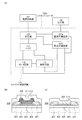
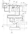
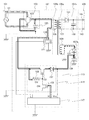
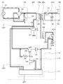
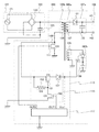
図1(A)に示すスイッチングコンバータ100aは、電源供給部101から与えられる電圧(入力電圧)を用いて、一定の電圧(出力電圧)を生成し、出力部109から一定の電圧を出力する。
A switching
スイッチングコンバータ100aは、変圧器105と、整流平滑回路107aと、整流平滑回路107bと、スイッチ111と、スイッチング制御回路113とを有する。なお、変圧器105は電源供給部101と接続する。また、整流平滑回路107aは出力部109と接続する。
The switching
スイッチング制御回路113は、スタータ回路115及び制御回路117を有する。
The switching
変圧器105は、整流平滑回路107a、整流平滑回路107b、及びスイッチ111と接続する。
The
整流平滑回路107aは、変圧器105、出力部109、及びスタータ回路115と接続する。整流平滑回路107bは、変圧器105、スタータ回路115、及び制御回路117と接続する。
The rectifying /
スタータ回路115は、整流平滑回路107b、スイッチ111、及び制御回路117と接続する。制御回路117は、整流平滑回路107b、スイッチ111、及びスタータ回路115と接続する。
The
電源供給部101は、出力部109に電力を供給する機構であり、代表的には、AC(alternating current)電源、DC(Direct current)電源、発電装置、一次電池、二次電池、キャパシタ等の電源装置を有する。また、電源装置が交流電源の場合は、電源装置及びスイッチングコンバータの間に整流平滑回路を設ける。
The
スイッチ111は、電源供給部101から出力された直流電流をパルス電流に変換して変圧器105から出力する機能を有する。スイッチ111のオンオフの切り替えを行うことによって、変圧器からパルス電流を出力することができる。スイッチ111の代表例としては、トランジスタがある。トランジスタとしては、シリコン、ゲルマニウム、シリコンゲルマニウム等の単結晶半導体基板または多結晶半導体基板を用いて形成されるトランジスタがある。また、後述するスタータ回路115に含まれるワイドギャップ半導体を用いて形成されるトランジスタがある。
The
変圧器105は、スイッチ111から出力されたパルス電流を利用して、電源供給部101から入力された電圧を所望の電圧に変換し、出力部109及びスイッチング制御回路113に出力する機能を有する。
The
変圧器105の代表例としては、第1のコイル、第2のコイル、及び磁芯で構成される変圧器がある。なお、変圧器を構成する第1のコイルの巻き数と、第2のコイルの巻き数との比により、出力部109及びスイッチング制御回路113に出力する電圧を変えることができる。例えば、第1のコイルの巻き数に対して、第2のコイルの巻き数を少なくすることで、入力電圧に対して小さい出力電圧が得られる降圧型とすることができる。一方、第1のコイルの巻き数に対して、第2のコイルの巻き数を多くすることで、入力電圧に対して大きい出力電圧が得られる昇圧型とすることができる。
A typical example of the
整流平滑回路107aは、変圧器105から出力されるパルス電流を整流し平滑化し、出力部109に出力する回路であり、代表的には、少なくとも整流素子及びコンデンサを有し、さらに抵抗素子を有してもよい。
The rectifying /
整流平滑回路107bは、変圧器105から出力されるパルス電流を整流し平滑化し、スイッチング制御回路113に出力する回路であり、代表的には、少なくとも整流素子及びコンデンサを有し、さらに抵抗素子を有してもよい。
The rectifying /
変圧器105は整流平滑回路107a及び整流平滑回路107bと接続する。このため、電源供給部101から出力された電圧を変換して出力部109及びスイッチング制御回路113に電圧を出力することが可能であり、スイッチング制御回路113を動作させるための電源供給部を別途設ける必要がなく、部品数の削減が可能である。
The
スタータ回路115は、整流平滑回路107bから出力された直流電流を用いて整流平滑回路107bに含まれるコンデンサに充電を行い、素早く制御回路117を動作状態とする機能を有する。即ち、制御回路117の起動を制御する機能を有する。また、制御回路117を動作状態とした後、高電流が制御回路117へ流れ込み、制御回路117が破壊されることを防ぐ機能を有する。スタータ回路115は、ワイドギャップ半導体を有するトランジスタ及びワイドギャップ半導体を有する抵抗素子を備える。
The
ワイドギャップ半導体とは、バンドギャップが2eV以上、好ましくは2.5eV以上、より好ましくは3eV以上である半導体であり、代表的には、窒化ガリウム、窒化アルミニウム、窒化インジウム等の化合物半導体、シリコンカーバイド、酸化物半導体等がある。酸化物半導体の代表例としては、In−Ga−Zn系酸化物半導体、酸化インジウム、インジウム錫酸化物、インジウムガリウム酸化物、インジウム亜鉛酸化物、酸化錫、酸化亜鉛、酸化ガリウムなどを用いることができる。 The wide gap semiconductor is a semiconductor having a band gap of 2 eV or more, preferably 2.5 eV or more, more preferably 3 eV or more. Typically, a compound semiconductor such as gallium nitride, aluminum nitride, or indium nitride, silicon carbide, or the like. And oxide semiconductors. As a typical example of an oxide semiconductor, an In—Ga—Zn-based oxide semiconductor, indium oxide, indium tin oxide, indium gallium oxide, indium zinc oxide, tin oxide, zinc oxide, gallium oxide, or the like is used. it can.
ここで、ワイドギャップ半導体の一例として酸化物半導体を有するトランジスタ及び抵抗素子の構造について、図1(B)及び図1(C)を用いて説明する。 Here, structures of a transistor including an oxide semiconductor as an example of a wide gap semiconductor and a resistor are described with reference to FIGS.
図1(B)は、酸化物半導体膜を有するトランジスタ200の断面図である。基板201上に設けられる絶縁膜203と、絶縁膜203上に形成される酸化物半導体膜205と、酸化物半導体膜205に接する一対の電極207と、絶縁膜203、酸化物半導体膜205、及び一対の電極207に接するゲート絶縁膜209と、ゲート絶縁膜209を介して酸化物半導体膜205と重なるゲート電極211とを有する。また、ゲート絶縁膜209及びゲート電極211を覆う絶縁膜213を有する。
FIG. 1B is a cross-sectional view of a
図1(C)は、酸化物半導体膜を有する抵抗素子220の断面図である。基板201上に設けられる絶縁膜203と、絶縁膜203上に形成される酸化物半導体膜225と、酸化物半導体膜225に接する一対の電極227とを有する。また、酸化物半導体膜225及び一対の電極227を覆うゲート絶縁膜209及び絶縁膜213を有してもよい。
FIG. 1C is a cross-sectional view of the
なお、酸化物半導体膜を有するトランジスタ及び酸化物半導体膜を有する抵抗素子の構成の詳細については、後述する。 Note that details of the structure of the transistor including the oxide semiconductor film and the resistance element including the oxide semiconductor film are described later.
トランジスタのチャネル領域がワイドギャップ半導体で形成されることで、トランジスタのソースまたはドレインに高電圧が印加されても、トランジスタの劣化及び破壊を抑えることができる。また、抵抗素子の一対の端子の間にワイドギャップ半導体を設けることで、一対の端子の一方に高電圧が印加されても、抵抗素子の劣化及び破壊を抑えることができる。この結果、スイッチングコンバータの劣化及び破壊を低減することができる。また、スタータ回路に含まれるトランジスタを、制御回路を構成する素子に用いられる半導体とは異なる半導体を用いたトランジスタ、代表的にはワイドギャップ半導体を用いたトランジスタを用いて作製することで、制御回路を構成する素子とスタータ回路に含まれるトランジスタを絶縁することが可能である。このため、ノイズカットのためのガードリングをスタータ回路に設ける必要がなく、スタータ回路及び該スタータ回路を有するスイッチングコンバータの小型化が可能である。 When the channel region of the transistor is formed using a wide gap semiconductor, deterioration and breakdown of the transistor can be suppressed even when a high voltage is applied to the source or drain of the transistor. In addition, by providing a wide gap semiconductor between the pair of terminals of the resistance element, deterioration and destruction of the resistance element can be suppressed even when a high voltage is applied to one of the pair of terminals. As a result, deterioration and destruction of the switching converter can be reduced. In addition, a transistor included in the starter circuit is manufactured using a transistor using a semiconductor different from a semiconductor used for an element included in the control circuit, typically a transistor using a wide gap semiconductor. And the transistor included in the starter circuit can be insulated. Therefore, it is not necessary to provide a guard ring for noise reduction in the starter circuit, and the starter circuit and the switching converter having the starter circuit can be downsized.
制御回路117は、スイッチ111のオン/オフの制御、及びスタータ回路115の動作状態の制御を行う回路である。
The
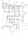
ここで、図1(A)に示すスイッチングコンバータ100aの具体的な回路構成について、図2を用いて説明する。
Here, a specific circuit configuration of the switching
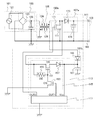
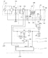
図2は、スイッチングコンバータ100aの一構成であるブーストコンバータ(昇圧型のコンバータ)の回路図である。なお、トランジスタ及び抵抗素子において、ワイドギャップ半導体の一例として酸化物半導体膜を用いた素子は、図2に示す回路図においてOSと付している。
FIG. 2 is a circuit diagram of a boost converter (step-up converter) that is one configuration of the switching
電源供給部101として、ここでは交流電源装置121及び整流平滑回路103を有する。整流平滑回路103として、整流素子123及びコンデンサ125を有する。ここでは、整流素子123の例としてダイオードブリッジを示す。
Here, the
スイッチ111は、ここではトランジスタ171を用いる。
The
変圧器105は、ここでは、対となるコイル126及びコイル129並びに磁芯(図示しない。)で構成される。
Here, the
整流平滑回路107aは、ここでは、ダイオード173及びコンデンサ175を有する。整流平滑回路107bは、ここでは、ダイオード166及びコンデンサ167を有する。
Here, the rectifying /
スタータ回路115は、ここでは、ワイドギャップ半導体を有するトランジスタ151、ワイドギャップ半導体を有するトランジスタ153、及びワイドギャップ半導体を有する抵抗素子155、及びダイオード157を有する。
Here, the
整流素子123の第1の端子及び第2の端子は交流電源装置121と接続する。整流素子123の第3の端子は、コンデンサ125の第1の端子と接続し、整流素子123の第4の端子はコンデンサ125の第2の端子及びグラウンドと接続する。コンデンサ125の第1の端子は、コイル126の第1の端子と接続する。
The first terminal and the second terminal of the rectifying
コイル126の第2の端子はトランジスタ171の第1の端子、ダイオード173の第1の端子、トランジスタ151の第1の端子、及び抵抗素子155の第1の端子と接続する。
The second terminal of the
ダイオード173の第2の端子は、コンデンサ175の第1の端子及び出力端子141と接続する。コンデンサ175の第2の端子は、トランジスタ171の第2の端子、出力端子143、コンデンサ125の第2の端子、整流素子123の第4の端子、及びグラウンドと接続する。
A second terminal of the
トランジスタ171のゲートは、制御回路117の出力端子OUT2と接続する。
The gate of the
コイル129の第1の端子は、ダイオード166の第1の端子と接続し、コイル129の第2の端子はグラウンドと接続する。ダイオード166の第2の端子はコンデンサ167の第1の端子と接続する。
The first terminal of the
トランジスタ151の第2の端子はダイオード157の第1の端子と接続し、トランジスタ151のゲートはトランジスタ153の第1の端子及び抵抗素子155の第2の端子と接続する。トランジスタ153のゲートは制御回路117の出力端子OUT1と接続し、トランジスタ153の第2の端子はグラウンドと接続する。ダイオード157の第2の端子は、制御回路117の端子Vcc、ダイオード166の第2の端子、及びコンデンサ167の第1の端子と接続する。
The second terminal of the
制御回路117はグラウンドと接続する。
The
コンデンサ167の第2の端子はグラウンドと接続する。
The second terminal of the
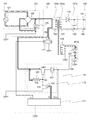
図1及び図2と異なる構造のスイッチングコンバータの構造について、図3及び図4を用いて説明する。 The structure of a switching converter having a structure different from that in FIGS. 1 and 2 will be described with reference to FIGS.
図3に示すスイッチングコンバータ100bは、電源供給部101と接続するスイッチ111と、スイッチ111と接続する変圧器105と、スイッチ111、変圧器105、出力部109、スイッチング制御回路113と接続する整流平滑回路107aと、変圧器105及びスイッチング制御回路113と接続する整流平滑回路107bと、電源供給部101、スイッチ111、整流平滑回路107a、及び整流平滑回路107bと接続するスイッチング制御回路113とを有する。
The switching
なお、図3に示すスイッチングコンバータ100bは、図1(A)とスイッチ111及び変圧器105の接続が異なるのみで、各回路、スイッチ、変圧器の構成は図1(A)と同様とすることができるため、詳細な説明を省略する。
Note that the switching
ここで、図3に示すスイッチングコンバータ100bの具体的な回路構成について、図4を用いて説明する。
Here, a specific circuit configuration of the switching
図4は、図3に示すスイッチングコンバータ100bの一構成であるバックコンバータ(降圧型のコンバータ)の回路図である。なお、トランジスタ及び抵抗素子において、ワイドギャップ半導体の一例として酸化物半導体膜を用いた素子は、図4に示す回路図においてOSと付している。
FIG. 4 is a circuit diagram of a buck converter (step-down converter) which is one configuration of switching
電源供給部101として、ここでは交流電源装置121及び整流平滑回路103を有する。
Here, the
整流平滑回路103として、整流素子123及びコンデンサ125を有する。ここでは、整流素子123としてダイオードブリッジの例を示す。
The rectifying /
スイッチ111は、ここではトランジスタ163を用いる。
The
変圧器105は、ここでは、対となるコイル126及びコイル129、並びに磁芯(図示しない。)で構成される。
Here, the
整流平滑回路107aは、ここでは、ダイオード164及びコンデンサ165を有する。整流平滑回路107bは、ここでは、ダイオード166及びコンデンサ167を有する。
Here, the rectifying /
スタータ回路115は、ここでは、ワイドギャップ半導体を有するトランジスタ151、ワイドギャップ半導体を有するトランジスタ153、及びワイドギャップ半導体を有する抵抗素子155、及びダイオード157を有する。
Here, the
整流素子123の第1の端子及び第2の端子は交流電源装置121と接続する。整流素子123の第3の端子は、コンデンサ125の第1の端子と接続し、整流素子123の第4の端子はコンデンサ125の第2の端子及びグラウンドと接続する。コンデンサ125の第1の端子は、抵抗素子161の第1の端子、トランジスタ163の第1の端子と接続する。
The first terminal and the second terminal of the rectifying
抵抗素子161の第2の端子は、トランジスタ163のゲートと接続する。トランジスタ163の第2の端子は、トランジスタ151の第1の端子、及び抵抗素子155の第1の端子と接続する。トランジスタ163の第2の端子は、ダイオード164の第1の端子及びコイル126の第1の端子と接続する。トランジスタ163のゲートは、制御回路117の出力端子OUT2と接続する。
A second terminal of the
ダイオード164の第1の端子はコイル126の第1の端子と接続し、ダイオード164の第2の端子はコンデンサ165の第2の端子及びグラウンドと接続する。
The first terminal of the
コイル126の第1の端子はダイオード164の第1の端子と接続し、コイル126の第2の端子はコンデンサ165の第1の端子及び出力端子141と接続する。
The first terminal of the
コンデンサ165の第1の端子は出力端子141と接続し、コンデンサ165の第2の端子は出力端子143、及びダイオード164の第2の端子と接続する。
A first terminal of the
コイル129の第1の端子はダイオード166の第1の端子と接続し、コイル129の第2の端子はグラウンドと接続する。
The first terminal of the
トランジスタ151の第2の端子はダイオード157の第1の端子と接続し、トランジスタ151のゲートはトランジスタ153の第1の端子及び抵抗素子155の第2の端子と接続する。トランジスタ153のゲートは制御回路117の出力端子OUT1と接続し、トランジスタ153の第2の端子はグラウンドと接続する。ダイオード157の第2の端子は、制御回路117の端子Vcc、ダイオード166の第2の端子、及びコンデンサ167の第1の端子と接続する。
The second terminal of the
制御回路117はグラウンドと接続する。
The
コンデンサ167の第2の端子はグラウンドと接続する。
The second terminal of the
次に、スイッチングコンバータの動作方法について、図5乃至図9を用いて説明する。ここでは、図2に示すスイッチングコンバータ100aを用いて説明する。なお、図5乃至図9において、電源供給部101から整流素子123に出力される交流電流を一点破線矢印で示し、整流素子123で変換された直流電流を実線矢印を用いて説明する。
Next, an operation method of the switching converter will be described with reference to FIGS. Here, description will be made using the
図5は、電源供給部101の電力供給時の様子を示す。
FIG. 5 shows a state when the
電源供給部101の交流電源装置121から出力された交流電流は、整流平滑回路103において、整流素子123によって整流され、コンデンサ125によって平滑化される。この結果、整流平滑回路103から、変圧器105に含まれるコイル126に直流電流が出力される。
The alternating current output from the alternating current
変圧器105のコイル126を流れる直流電流は、スイッチング制御回路113に含まれるスタータ回路115に出力される。このとき、スタータ回路115の抵抗素子155及びトランジスタ151の第1の端子には高電位が印加され、抵抗素子155に電荷が蓄積される。この結果、抵抗素子155の第2の端子と接続するトランジスタ151のゲートに高電位が印加され、トランジスタ151がオン状態となる。なお、抵抗素子155を介してトランジスタ151のゲートに出力される直流電流は、抵抗素子155に出力される直流電流と比較して、電流値が低いため、トランジスタ151のゲートに出力される直流電流を破線矢印で示す。また、トランジスタ153のゲートは制御回路117と接続されているが、制御回路117の端子Vccに電圧が印加されていないため制御回路117は動作しない。そのため、制御回路117の出力端子OUT1及び出力端子OUT2からは電流が出力されず、トランジスタ153及びトランジスタ171のゲートは低電位(L)である。このため、トランジスタ153及びトランジスタ171はオフ状態である。
The direct current flowing through the
トランジスタ151がオン状態となると、スタータ回路115のダイオード157で整流された直流電流は、整流平滑回路107bのコンデンサ167に出力され、コンデンサ167が充電される。
When the
図6は、制御回路117の立ち上げ時の様子を示す。
FIG. 6 shows a state when the
整流平滑回路107bのコンデンサ167が充電されると、制御回路117の端子Vccの電位が制御回路117の動作電位まで上昇する。この結果、制御回路117の出力端子OUT1からスタータ回路115のトランジスタ153をオン状態とさせる電流が出力され、トランジスタ153のゲートに高電位(H)が印加され、スタータ回路115のトランジスタ153がオン状態となる。なお、ここで、出力端子OUT2から高速にオン/オフするCLK信号をスイッチ111のトランジスタ171のゲートに出力すると、コンデンサ167で充電された電荷が消滅してしまうため、出力端子OUT2からトランジスタ171のゲートには低電位(L)が印加される。
When the
図7は、スタータ回路115の停止時の様子を示す。
FIG. 7 shows a state when the
スタータ回路115のトランジスタ153がオン状態となると、トランジスタ153の第2の端子はグラウンドと接続されているため、トランジスタ153の第1の端子がグラウンドと同電位となり、トランジスタ151のゲートがグラウンドと同電位となり、トランジスタ151がオフ状態となる。この結果、変圧器105から出力される電流がトランジスタ151で遮断され、スタータ回路115の動作が停止する。
When the
なお、このときトランジスタ151の第1の端子には、コイル126の電位と同等の高電位が印加され、トランジスタ151の第2の端子は制御回路117の動作電位と同電位が印加される。また、スタータ回路115の抵抗素子155の第1の端子には、コイル126の電位と同等の高電位が印加され、抵抗素子155の第2の端子はオン状態のトランジスタ153を介してグラウンドと同電位である。このため、トランジスタ151及び抵抗素子155をワイドギャップ半導体、ここでは酸化物半導体膜を用いて高耐圧の装置を形成することで、トランジスタ151及び抵抗素子155の破壊及び劣化を抑制することができる。また、トランジスタ151を、制御回路を構成する素子に用いられる半導体とは異なる半導体を用いたトランジスタ、代表的にはワイドギャップ半導体を用いたトランジスタを用いて作製することで、制御回路を構成する素子とトランジスタ151を絶縁することが可能である。このため、ノイズカットのためのガードリングをスタータ回路に設ける必要がなく、スタータ回路及び該スタータ回路を有するスイッチングコンバータの小型化が可能である。
At this time, a high potential equivalent to the potential of the
図8は、スイッチ111のトランジスタ171へのCLK信号供給開始時の様子を示す。
FIG. 8 shows a state at the start of supplying a CLK signal to the
スタータ回路115のトランジスタ151がオフ状態となることで、整流平滑回路107bのコンデンサ167への充電が停止するが、整流平滑回路107bのコンデンサ167からの充電により、コンデンサ167から制御回路117に直流電流が流れ、制御回路117の端子Vccの電位が動作電位にまで上昇し、制御回路117が動作状態となる。この結果、制御回路117からスタータ回路115のトランジスタ171のゲートにCLK信号が出力されるため、トランジスタ171を高速にスイッチングすることができる。
When the
図9は、スイッチングコンバータ100aの定常動作時の様子を示す。
FIG. 9 shows a state during the steady operation of the switching
スイッチ111のトランジスタ171のオン/オフの繰り返しにより、整流平滑回路103から変圧器105にパルス状の直流電流が流れる。この結果、整流平滑回路107aに直流電流が出力されると共に、整流平滑回路107bに、直流電流が出力される。整流平滑回路107aでは、ダイオード173で整流された後、コンデンサ175で平滑化され、出力部109の出力端子141に出力される。また、整流平滑回路107bでは、ダイオード166で整流されたのち、コンデンサ167で平滑化され、制御回路117に出力される。この結果、出力部109に電圧値が変換された電圧を出力することができる。また、変圧器105から制御回路117に電圧値が変換された電圧を出力することができる。このため、別途電源供給部を設けずとも、制御回路117を動作させることができる。
By repeating ON / OFF of the
スタータ回路に含まれるトランジスタのチャネル領域がワイドギャップ半導体で形成されることで、トランジスタのソースまたはドレインに高電圧が印加されても、トランジスタの劣化及び破壊を抑えることができる。また、抵抗素子の一対の端子の間にワイドギャップ半導体を設けることで、一対の端子の一方に高電圧が印加されても、抵抗素子の劣化及び破壊を抑えることができる。この結果、スイッチングコンバータの劣化及び破壊を低減することができる。また、スタータ回路に含まれるトランジスタを、制御回路を構成する素子に用いられる半導体とは異なる半導体を用いたトランジスタ、代表的にはワイドギャップ半導体を用いたトランジスタを用いて作製することで、制御回路を構成する素子とスタータ回路に含まれるトランジスタを絶縁することが可能である。このため、ノイズカットのためのガードリングをスタータ回路に設ける必要がなく、スタータ回路及び該スタータ回路を有するスイッチングコンバータの小型化が可能である。 By forming the channel region of the transistor included in the starter circuit using a wide gap semiconductor, deterioration and breakdown of the transistor can be suppressed even when a high voltage is applied to the source or drain of the transistor. In addition, by providing a wide gap semiconductor between the pair of terminals of the resistance element, deterioration and destruction of the resistance element can be suppressed even when a high voltage is applied to one of the pair of terminals. As a result, deterioration and destruction of the switching converter can be reduced. In addition, a transistor included in the starter circuit is manufactured using a transistor using a semiconductor different from a semiconductor used for an element included in the control circuit, typically a transistor using a wide gap semiconductor. And the transistor included in the starter circuit can be insulated. Therefore, it is not necessary to provide a guard ring for noise reduction in the starter circuit, and the starter circuit and the switching converter having the starter circuit can be downsized.
なお、スイッチ111としてワイドギャップ半導体を有するトランジスタを用いたスイッチングコンバータ110の回路図を図10に示す。ここでは、図4に示すスイッチングコンバータ100bを用いて説明するが、適宜図2に示すスイッチングコンバータ100aを用いてもよい。また、ワイドギャップ半導体の一例として酸化物半導体膜を用いたトランジスタ170をスイッチ111に設けたため、図10に示す回路図においてトランジスタ170にOSと付している。
A circuit diagram of the switching
スイッチング制御回路113に含まれるスタータ回路115と同様に、ワイドギャップ半導体を用いてトランジスタ170は形成されるため、スイッチング制御回路113にスイッチ111を設けることができる。この結果、スイッチングコンバータ110の部品数を削減することが可能である。
Similarly to the
また、ワイドギャップ半導体を有するトランジスタは、オフ電流が極めて低く、なおかつ高耐圧である。このため、トランジスタ170として、ワイドギャップ半導体を有するトランジスタを用いることで、電源供給部からの高電圧の印加によるオフ電流を低減することが可能であり、スイッチングコンバータの電力変換効率を向上させることができる。また、スイッチングコンバータの電力変換効率を向上させることで、スイッチングコンバータを用いた半導体装置の消費電力を抑えることができる。
In addition, a transistor including a wide gap semiconductor has extremely low off-state current and high withstand voltage. Therefore, by using a transistor having a wide gap semiconductor as the
(実施の形態2)
図11及び図12を用いて、本発明の一態様に係るスイッチングコンバータの構成を説明する。本実施の形態では、絶縁型のスイッチングコンバータの構造について説明する。
(Embodiment 2)
The structure of the switching converter according to one embodiment of the present invention is described with reference to FIGS. In this embodiment, a structure of an insulating switching converter will be described.
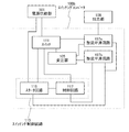
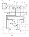
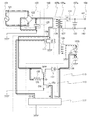
図11に示すスイッチングコンバータ180は、変圧器105と、整流平滑回路107aと、整流平滑回路107bと、スイッチ111と、スイッチング制御回路113とを有する。なお、変圧器105は電源供給部101と接続する。また、整流平滑回路107aは出力部109と接続する。
A switching
変圧器105は、変圧器105a及び変圧器105bを有する。スイッチング制御回路113は、スタータ回路115及び制御回路117を有する。
The
変圧器105aは、整流平滑回路107a、及びスイッチ111と接続する。変圧器105bは、整流平滑回路107b、及びスイッチ111と接続する。
The
整流平滑回路107aは、変圧器105a及び出力部109と接続する。整流平滑回路107bは、変圧器105b、スタータ回路115、及び制御回路117と接続する。
The rectifying /
スタータ回路115は、整流平滑回路107b、スイッチ111、及び制御回路117と接続する。制御回路117は、整流平滑回路107b、スイッチ111、及びスタータ回路115と接続する。
The
図11に示すスイッチングコンバータ180の各回路、スイッチ、変圧器の構成は図1(A)と同様とすることができるため、既出の構成の詳細な説明を省略する。
Since the configuration of each circuit, switch, and transformer of the switching
変圧器105aは、スイッチ111から出力されたパルス電流を利用して、電源供給部101から入力された電圧を所望の電圧に変換し、出力部109に出力する機能を有する。変圧器105aの代表例としては、第1のコイル、第2のコイル、及び磁芯で構成される変圧器がある。
The
変圧器105bは、スイッチ111から出力されたパルス電流を利用して、電源供給部101から入力された電圧を所望の電圧に変換し、スイッチング制御回路113に出力する機能を有する。変圧器105bの代表例としては、第1のコイル、第3のコイル、及び磁芯で構成される変圧器がある。
The
変圧器105aは第1のコイル及び第2のコイルを有し、変圧器105bは第1のコイル及び第3のコイルを有するため、電源供給部101から出力された電圧を変換して出力部109及びスイッチング制御回路113に電圧を出力することが可能であり、スイッチング制御回路113を動作させるための電源供給部を別途設ける必要がない。また、第1のコイルの巻き数と、第2のコイル及び第3のコイルの巻き数との比により、出力部109及びスイッチング制御回路113に出力する電圧を変えることができる。例えば、第1のコイルの巻き数に対して、第2のコイル及び第3のコイルのそれぞれの巻き数を少なくすることで、入力電圧に対して小さい出力電圧が得られる降圧型とすることができる。一方、第1のコイルの巻き数に対して、第2のコイル及び第3のコイルのそれぞれの巻き数を多くすることで、入力電圧に対して大きい出力電圧が得られる昇圧型とすることができる。
Since the
スタータ回路115は、電源供給部101から出力された直流電流を用いて整流平滑回路107bに含まれるコンデンサに充電を行い、素早く制御回路117を動作状態とするための回路である。即ち、制御回路117の起動を制御する機能を有する。また、制御回路117を動作状態とした後、高電流が制御回路117へ流れ込み、制御回路117が破壊されることを防ぐ機能を有する回路である。スタータ回路115は、ワイドギャップ半導体を有するトランジスタ及びワイドギャップ半導体を有する抵抗素子を備える。
The
ワイドギャップ半導体を有するトランジスタ及びワイドギャップ半導体を有する抵抗素子は、実施の形態1に示す酸化物半導体膜を有するトランジスタ200及び抵抗素子220を適宜用いることができる。
As the transistor having a wide gap semiconductor and the resistor having a wide gap semiconductor, the
トランジスタのチャネル領域がワイドギャップ半導体で形成されることで、トランジスタのソースまたはドレインに高電圧が印加されても、トランジスタの劣化及び破壊を抑えることができる。また、抵抗素子の一対の端子の間にワイドギャップ半導体を設けることで、一対の端子の一方に高電圧が印加されても、抵抗素子の劣化及び破壊を抑えることができる。この結果、スイッチングコンバータの劣化及び破壊を低減することができる。また、スタータ回路に含まれるトランジスタを、制御回路を構成する素子に用いられる半導体とは異なる半導体を用いたトランジスタ、代表的にはワイドギャップ半導体を用いたトランジスタを用いて作製することで、制御回路を構成する素子とスタータ回路に含まれるトランジスタを絶縁することが可能である。このため、ノイズカットのためのガードリングをスタータ回路に設ける必要がなく、スタータ回路及び該スタータ回路を有するスイッチングコンバータの小型化が可能である。 When the channel region of the transistor is formed using a wide gap semiconductor, deterioration and breakdown of the transistor can be suppressed even when a high voltage is applied to the source or drain of the transistor. In addition, by providing a wide gap semiconductor between the pair of terminals of the resistance element, deterioration and destruction of the resistance element can be suppressed even when a high voltage is applied to one of the pair of terminals. As a result, deterioration and destruction of the switching converter can be reduced. In addition, a transistor included in the starter circuit is manufactured using a transistor using a semiconductor different from a semiconductor used for an element included in the control circuit, typically a transistor using a wide gap semiconductor. And the transistor included in the starter circuit can be insulated. Therefore, it is not necessary to provide a guard ring for noise reduction in the starter circuit, and the starter circuit and the switching converter having the starter circuit can be downsized.
ここで、図11に示すスイッチングコンバータ180の具体的な回路構成について、図12を用いて説明する。
Here, a specific circuit configuration of the switching
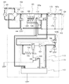
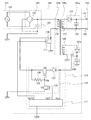
図12は、スイッチングコンバータ180の一構成であるフライバックコンバータの回路図である。なお、トランジスタ及び抵抗素子において、ワイドギャップ半導体の一例として酸化物半導体膜を用いた素子は、図12に示す回路図においてOSと付している。
FIG. 12 is a circuit diagram of a flyback converter that is one configuration of the switching
電源供給部101として、ここでは交流電源装置121及び整流平滑回路103を示す。整流平滑回路103として、整流素子123及びコンデンサ125を有する。ここでは、整流素子123としてダイオードブリッジを示す。
Here, an AC
変圧器105aは、ここでは、対となるコイル126及びコイル127で構成される。変圧器105bは、ここでは、対となるコイル126及びコイル129で構成される。
Here, the
整流平滑回路107aは、ここでは、ダイオード131及びコンデンサ133を有する。整流平滑回路107bは、ここでは、ダイオード137、及びコンデンサ139を有する。
Here, the rectifying /
スイッチ111は、ここではトランジスタ159を用いる。
The
スタータ回路115は、ここでは、ワイドギャップ半導体を有するトランジスタ151、ワイドギャップ半導体を有するトランジスタ153、及びワイドギャップ半導体を有する抵抗素子155、及びダイオード157を有する。
Here, the
整流素子123の第1の端子及び第2の端子は交流電源装置121と接続する。整流素子123の第3の端子は、コンデンサ125の第1の端子と接続し、整流素子123の第4の端子はコンデンサ125の第2の端子及びグラウンドと接続する。コンデンサ125の第1の端子はコイル126の第1の端子と接続する。コイル126の第2の端子は、トランジスタ159の第1の端子、トランジスタ151の第1の端子、及び抵抗素子155の第1の端子と接続する。
The first terminal and the second terminal of the rectifying
トランジスタ159の第2の端子はグラウンドと接続し、ゲートは制御回路117の出力端子OUT2と接続する。
A second terminal of the
コイル127の第1の端子はダイオード131の第1の端子と接続する。ダイオード131の第2の端子はコンデンサ133の第1の端子と接続する。コイル127の第2の端子はコンデンサ133の第2の端子と接続する。コンデンサ133の第1の端子は出力部109の出力端子141と接続し、コンデンサ133の第2の端子は出力端子143に接続する。
The first terminal of the
コイル129の第1の端子はダイオード137の第1の端子と接続し、第2の端子はグラウンドと接続する。ダイオード137の第2の端子はコンデンサ139の第1の端子と接続する。
The first terminal of the
コンデンサ139の第2の端子はグラウンドと接続する。
The second terminal of the
トランジスタ151の第2の端子はダイオード157の第1の端子と接続し、トランジスタ151のゲートはトランジスタ153の第1の端子及び抵抗素子155の第2の端子と接続する。トランジスタ153のゲートは制御回路117の出力端子OUT1と接続し、トランジスタ153の第2の端子はグラウンドと接続する。ダイオード157の第2の端子は、制御回路117の端子Vcc及びコンデンサ139の第1の端子と接続する。
The second terminal of the
制御回路117はグラウンドと接続する。
The
次に、スイッチングコンバータの動作方法について、図13乃至図17を用いて説明する。なお、図13乃至図17において、電源供給部101からスイッチングコンバータ180に出力される交流電流を一点破線矢印で示し、整流素子123で変換された直流電流を実線矢印を用いて説明する。
Next, an operation method of the switching converter will be described with reference to FIGS. In FIG. 13 to FIG. 17, the alternating current output from the
図13は、電源供給部101の電力供給時の様子を示す。
FIG. 13 shows a state when the
電源供給部101の交流電源装置121から出力された交流電流は、整流平滑回路103の整流素子123によって整流され、コンデンサ125によって平滑化される。この結果、整流平滑回路103から、変圧器105a及び変圧器105bに含まれるコイル126に直流電流が出力される。
The alternating current output from the alternating current
変圧器105a及び変圧器105bのコイル126を流れる直流電流は、スイッチング制御回路113に含まれるスタータ回路115に出力される。このとき、スタータ回路115の抵抗素子155及びトランジスタ151の第1の端子には高電位が印加され、抵抗素子155の第2の端子と接続するトランジスタ151のゲートに高電位が印加され、トランジスタ151がオン状態となる。なお、抵抗素子155を介してトランジスタ151のゲートに供給される直流電流は、抵抗素子155に入力される直流電流と比較して、電流値が低いため、直流電流を破線矢印で示す。また、トランジスタ153のゲートは制御回路117と接続されているが、制御回路117の端子Vccが0Vであるため、出力端子OUT1及び出力端子OUT2からは電流が出力されず、トランジスタ153及びトランジスタ159のゲートは低電位(L)である。このため、トランジスタ153及びトランジスタ159はオフ状態である。
The direct current flowing through the
トランジスタ151がオン状態となると、スタータ回路115のダイオード157で整流された直流電流は、整流平滑回路107bのコンデンサ139に出力され、コンデンサ139が充電される。
When the
なお、破線矢印は、変圧器105bから整流平滑回路107bのコンデンサ139に流れる電流を表す。コイル126及びコイル129を有する変圧器105bにおいて電圧が発生するが、当該電圧が低いため、変圧器105bからコンデンサ139に流れる電流を破線矢印で示す。
The broken line arrow represents the current flowing from the
図14は、制御回路117の立ち上げ時の様子を示す。
FIG. 14 shows a state when the
整流平滑回路107bのコンデンサ139が充電されると、制御回路117の端子Vccの電位が制御回路117の動作電位まで上昇する。この結果、制御回路117の出力端子OUT1からスタータ回路115のトランジスタ153のゲートにトランジスタ153をオン状態とする電流が出力され、トランジスタ153のゲートに高電位(H)が印加され、スタータ回路115のトランジスタ153がオン状態となる。なお、ここで、出力端子OUT2からトランジスタ159を高速にオン/オフするCLK信号をスイッチ111のトランジスタ159のゲートに出力すると、コンデンサ139で充電された電荷が消滅してしまうため、トランジスタ159のゲートは低電位(L)である。
When the
図15は、スタータ回路115の停止時の様子を示す。
FIG. 15 shows a state when the
スタータ回路115のトランジスタ153がオン状態となると、トランジスタ153の第2の端子はグラウンドと接続されているため、トランジスタ153の第1の端子がグラウンドと同電位となり、トランジスタ151のゲートがグラウンドと同電位となり、トランジスタ151がオフ状態となる。この結果、変圧器105aから出力される電流がトランジスタ151で遮断され、スタータ回路115の動作が停止する。
When the
なお、このときトランジスタ151の第1の端子には、コイル126の電位と同等の高電位が印加され、トランジスタ151の第2の端子は制御回路117の動作電位と同電位が印加される。また、スタータ回路115の抵抗素子155の第1の端子には、コイル126の電位と同等の高電位が印加され、抵抗素子155の第2の端子はオン状態のトランジスタ153を介してグラウンドと同電位である。このため、トランジスタ151及び抵抗素子155を高耐圧のワイドギャップ半導体、ここでは酸化物半導体膜を用いてデバイスを形成することで、トランジスタ151及び抵抗素子155の破壊及び劣化を抑制することができる。また、トランジスタ151を、制御回路を構成する素子に用いられる半導体とは異なる半導体を用いたトランジスタ、代表的にはワイドギャップ半導体を用いたトランジスタを用いて作製することで、制御回路を構成する素子とトランジスタ151を絶縁することが可能である。このため、ノイズカットのためのガードリングをスタータ回路に設ける必要がなく、スタータ回路及び該スタータ回路を有するスイッチングコンバータの小型化が可能である。
At this time, a high potential equivalent to the potential of the
図16は、スイッチ111のトランジスタ159へのCLK信号供給開始時の様子を示す。
FIG. 16 shows a state at the start of supplying a CLK signal to the
スタータ回路115のトランジスタ151がオフ状態となることで、整流平滑回路107bのコンデンサ139への充電が停止するが、整流平滑回路107bのコンデンサ139からの充電により、コンデンサ139から制御回路117に直流電流が流れ、制御回路117の端子Vccの電位が動作電位にまで上昇し、制御回路117が動作状態となる。この結果、制御回路117からスタータ回路115のトランジスタ159のゲートにCLK信号が出力されるため、トランジスタ159を高速にスイッチングすることができる。
When the
図17は、スイッチングコンバータ180の定常動作時の様子を示す。
FIG. 17 shows a state during the steady operation of the switching
スイッチ111のトランジスタ159のオン/オフの繰り返しにより、整流平滑回路103から変圧器105a及び変圧器105bにパルス状の直流電流が流れる。また、整流平滑回路107aに直流電流が出力されると共に、整流平滑回路107bに、直流電流が出力される。整流平滑回路107aでは、ダイオード131で整流された後、コンデンサ133で平滑化され、出力部109の出力端子141及び出力端子143に出力される。整流平滑回路107bでは、ダイオード137で整流され、コンデンサ139で平滑化され、制御回路117に出力される。この結果、変圧器105aから出力部109に電圧値が変換された電圧を出力することができる。また、変圧器105bから制御回路117に電圧値が変換された電圧を出力することができる。このため、別途電源供給部を設けずとも、制御回路117を動作させることができる。
By repeating ON / OFF of the
なお、スイッチ111としてワイドギャップ半導体を有するトランジスタを用いたスイッチングコンバータ190の回路図を図18に示す。ここでは、ワイドギャップ半導体の一例として酸化物半導体膜を用いたトランジスタ169をスイッチ111に設けたため、図18に示す回路図においてトランジスタ169にOSと付している。
A circuit diagram of a switching
スイッチング制御回路113に含まれるスタータ回路115と同様に、ワイドギャップ半導体を用いてトランジスタ169は形成されるため、スイッチング制御回路113にスイッチ111を設けることができる。この結果、スイッチングコンバータ160の部品数を削減することが可能である。
Similarly to the
また、トランジスタ170として、ワイドギャップ半導体を有するトランジスタを用いることで、電源供給部からの高電圧の印加によるオフ電流を低減することが可能であり、スイッチングコンバータの電力変換効率を向上させることができる。また、スイッチングコンバータの電力変換効率を向上させることで、スイッチングコンバータを用いた半導体装置の消費電力を抑えることができる。
Further, by using a transistor having a wide gap semiconductor as the
なお、本実施の形態では、絶縁型のスイッチングコンバータの一例としてフライバックコンバータを用いて説明したが、適宜、フォワードコンバータ、ハーフブリッジコンバータ、フルブリッジコンバータを適用することができる。 Note that although a flyback converter has been described as an example of an insulating switching converter in this embodiment, a forward converter, a half bridge converter, and a full bridge converter can be applied as appropriate.
本実施の形態は、他の実施の形態と適宜組み合わせて実施することが可能である。 This embodiment can be implemented in appropriate combination with any of the other embodiments.
(実施の形態3)
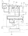
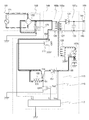
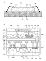
本実施の形態では、スイッチングコンバータ180に含まれるスイッチング制御回路113の構造について、図19を用いて説明する。なお、図19は、図12に示すスイッチング制御回路113のトランジスタ151、トランジスタ153、抵抗素子155、ダイオード157、及び制御回路117に含まれるCMOS(Complementary Metal−Oxide Semiconductor)回路の断面図である。
(Embodiment 3)
In this embodiment, the structure of switching
図19(A)は、スイッチング制御回路760の断面図である。接地された部材761上にスタータ回路115及び制御回路117を有するスイッチング制御回路760が設けられる。スイッチング制御回路760は、半導体基板で形成されたトランジスタ、ダイオード(代表的には、実施の形態1及び実施の形態2に示すスタータ回路115に含まれるダイオード157)等を有する素子層763aと、素子層763a上に設けられたワイドギャップ半導体を有するトランジスタ及び抵抗素子(代表的には、実施の形態1及び実施の形態2に示すスタータ回路115に含まれるトランジスタ151、トランジスタ153、及び抵抗素子155)を有する素子層763bを有する。
FIG. 19A is a cross-sectional view of the switching
素子層763b上には、端子765、775が形成されており、端子765、775と接地された部材761とが、それぞれ導電部材769、779で接続されている。端子765、775は、アルミニウムまたはアルミニウム合金で形成されている。導電部材769、779として、ここでは、金、金を含む合金、銅、または銅を含む合金で形成された金属の細線(ワイヤー)を用いる。
図19(B)は、スイッチング制御回路760の一部の拡大断面図である。素子層763aに設けられる半導体基板701は、シリコン、ゲルマニウム、シリコンゲルマニウム、炭化シリコン、またはガリウムヒ素を用いた単結晶半導体または多結晶半導体を用いることが好ましい。単結晶半導体を用いたトランジスタは、高速動作が容易である。一方、素子層763bに設けられるトランジスタ750及び抵抗素子751は、ワイドギャップ半導体を有する。このため、トランジスタ750及び抵抗素子751に高電圧が印加されても、トランジスタ750及び抵抗素子751の劣化及び破壊を抑えることができる。また、トランジスタ750のチャネル領域がワイドギャップ半導体で形成されることで、トランジスタ750のオフ電流を低減することが可能であり、スイッチングコンバータの電力損失を小さく抑え、電力変換効率の低減を防ぐことができる。
FIG. 19B is an enlarged cross-sectional view of a part of the switching
素子層763bには、図12に示すスタータ回路115に含まれる素子が形成される。スイッチングコンバータ180が定常動作している場合、スイッチ111のオン/オフと共に、抵抗素子155の第1の端子に高電位及び低電位が交互に印加される。この結果、抵抗素子155の第2の端子と接続するトランジスタ153の第1の端子の電位が上下してしまう。ここで、トランジスタ153はオン状態であるため、トランジスタ153に接続するグラウンドにノイズが発生する。当該グラウンドと、制御回路117が接続するグラウンドを直接接続すると、ノイズが制御回路117に入力され、制御回路117の動作に不具合が生じる。一方、図19に示すスイッチング制御回路760は、素子層763aが、接地された部材761と直接接続する。または、素子層763aが、接地された部材761と導電性部材を介して電気的に接続する。また、素子層763bが、導電部材769、779を介して接地された部材761と電気的に接続する。制御回路117が形成される素子層763a、及びトランジスタ153が形成される素子層763bの両方が、接地された部材761と直接接続せず、少なくとも一方が導電部材を介して接地された部材761と電気的に接続する。ここでは、素子層763bが導電部材769、779を介して接地された部材761と電気的に接続している。このため、同一の半導体基板に制御回路117及びトランジスタ153が形成される場合と比較して、トランジスタ153で発生するノイズが制御回路117に伝達することを抑制することができる。
In the
素子層763aに含まれるトランジスタ704a及びトランジスタ704bは、それぞれnチャネル型トランジスタ(NMOSFET)及びpチャネル型トランジスタ(PMOSFET)である。ここでは、トランジスタ704aとしてnチャネル型のトランジスタを示し、トランジスタ704bとしてpチャネル型のトランジスタを示す。図19(B)に示す例においては、トランジスタ704a及びトランジスタ704bは、STI(Shallow Trench Isolation)702によって他の素子と絶縁分離されている。STI702を用いることにより、LOCOSによる素子分離法で発生した素子分離部のバーズビークを抑制することができ、素子分離部の縮小等が可能となる。一方で、構造の微細化小型化が要求されない半導体装置においてはSTI702の形成は必ずしも必要ではなく、LOCOS等の素子分離手段を用いることもできる。
The
トランジスタ704a及びトランジスタ704bは、それぞれ半導体基板701中に設けられたチャネル形成領域と、チャネル形成領域を挟むように設けられた不純物領域705(ソース領域及びドレイン領域ともいう)と、チャネル形成領域上に設けられたゲート絶縁膜706と、ゲート絶縁膜706上にチャネル形成領域と重畳するように設けられたゲート電極707とを有する。ゲート電極707は単層または多層とすることができる。なお、ゲート電極707を、加工精度を高めるための第1の材料からなる第1の導電膜と、低抵抗化を目的とした第2の材料からなる第2の導電膜との積層構造としてもよい。
The
また、半導体基板701中に設けられた不純物領域705には、コンタクトプラグ714が接続されている。ここでコンタクトプラグ714は、トランジスタ704a、704bのソース電極やドレイン電極としても機能する。また、不純物領域705とチャネル領域の間には、不純物領域705と異なる不純物領域が設けられている。該不純物領域は、導入された不純物の濃度によって、LDD領域やエクステンション領域としてチャネル形成領域近傍の電界分布を制御する機能を果たす。ゲート電極707の側壁にはサイドウォール絶縁膜710を有する。サイドウォール絶縁膜710を用いることで、LDD領域やエクステンション領域を形成することができる。
A
また、トランジスタ704a及びトランジスタ704bは、絶縁膜711により被覆されている。絶縁膜711には保護膜としての機能を持たせることができ、外部からチャネル形成領域への不純物の侵入を防止することができる。また、絶縁膜711をCVD法による窒化シリコン等の材料とすることで、チャネル形成領域に単結晶シリコンを用いた場合には加熱処理によって脱水素化を行うことができる。また、絶縁膜711に引張応力または圧縮応力を有する絶縁膜を用いることで、チャネル形成領域を構成する半導体材料に歪みを与えることができる。nチャネル型のトランジスタの場合にはチャネル形成領域となるシリコン材料に引張応力を、pチャネル型のトランジスタの場合にはチャネル形成領域となるシリコン材料に圧縮応力を付加することで、各トランジスタの移動度を向上させることができる。
The
ダイオード704cは、p型またはn型の一方を呈する不純物領域717と、p型またはn型の他方を呈する不純物領域718とが接合するダイオードである。不純物領域717、不純物領域718は、トランジスタ704a、トランジスタ704bの不純物領域を形成するときに、同時に形成することができる。ダイオード704cの不純物領域717、不純物領域718のそれぞれには、コンタクトプラグ714が接続される。
The
素子層763bには、素子層763aに接するバリア膜724、バリア膜724上に形成される絶縁膜725、絶縁膜725上に形成されるトランジスタ750及び抵抗素子751を有する。
The
バリア膜724は、水素、水、及び酸素のブロッキング効果を有する絶縁膜で形成することが好ましく、代表的には酸化アルミニウム膜で形成する。
The
絶縁膜725は、加熱により酸素の一部が脱離する酸化絶縁膜を用いて形成することが好ましい。加熱により酸素の一部が脱離する酸化絶縁膜としては、化学量論的組成を満たす酸素よりも多くの酸素を含む酸化絶縁膜を用いることが好ましい。加熱により酸素の一部が脱離する酸化絶縁膜は、加熱処理により酸化物半導体膜に酸素を拡散させることができる。絶縁膜725の代表例としては、酸化シリコン、酸化窒化シリコン、窒化酸化シリコン、酸化ガリウム、酸化ハフニウム、酸化イットリウム、酸化アルミニウム、酸化窒化アルミニウム等がある。
The insulating
絶縁膜725は、50nm以上、好ましくは200nm以上3000nm以下、好ましくは300nm以上1000nm以下とする。絶縁膜725を厚くすることで、絶縁膜725の酸素脱離量を増加させることができると共に、絶縁膜725及び後に形成される酸化物半導体膜との界面における界面準位を低減することが可能である。
The insulating
ここで、「加熱により酸素の一部が脱離する」とは、TDS(Thermal Desorption Spectroscopy:昇温脱離ガス分光法)分析にて、酸素原子に換算しての酸素の放出量が1.0×10¹⁸atoms/cm3以上、好ましくは3.0×1020atoms/cm3以上であることをいう。 Here, “a part of oxygen is desorbed by heating” means that the amount of released oxygen converted to oxygen atoms in a TDS (Thermal Desorption Spectroscopy) analysis is 1. It means 0 × 10 18 atoms / cm 3 or more, preferably 3.0 × 10 20 atoms / cm 3 or more.
上記構成において、加熱により酸素放出される絶縁膜は、酸素が過剰な酸化シリコン(SiOX(X>2))であってもよい。酸素が過剰な酸化シリコン(SiOX(X>2))とは、シリコン原子数の2倍より多い酸素原子を単位体積当たりに含むものである。単位体積当たりのシリコン原子数及び酸素原子数は、ラザフォード後方散乱法により測定した値である。 In the above structure, the insulating film from which oxygen is released by heating may be oxygen-excess silicon oxide (SiO X (X> 2)). Oxygen-excess silicon oxide (SiO X (X> 2)) contains oxygen atoms more than twice the number of silicon atoms per unit volume. The number of silicon atoms and the number of oxygen atoms per unit volume are values measured by Rutherford backscattering method.
トランジスタ750は、図1(B)に示すトランジスタ200と同様の構造のトランジスタを用いることができる。抵抗素子751は図1(C)に示す抵抗素子220と同様の構造の抵抗素子220を用いることができる。
As the
トランジスタ200の詳細な構造を、図1(B)を用いて説明する。なお、図19(B)に示す絶縁膜725は図1(B)の絶縁膜203に相当する。
A detailed structure of the
トランジスタ200は、絶縁膜203上に形成される酸化物半導体膜205と、酸化物半導体膜205に接する一対の電極207と、絶縁膜203、酸化物半導体膜205、及び一対の電極207に接するゲート絶縁膜209と、ゲート絶縁膜209を介して酸化物半導体膜205と重なるゲート電極211とを有する。また、ゲート絶縁膜209及びゲート電極211を覆う絶縁膜213を有する。
The
酸化物半導体膜205は、少なくともインジウム(In)若しくは亜鉛(Zn)を含むことが好ましい。または、InとZnの双方を含むことが好ましい。また、該酸化物半導体を用いたトランジスタの電気特性のばらつきを減らすため、それらと共に、スタビライザーの一または複数を有することが好ましい。
The
スタビライザーとしては、ガリウム(Ga)、スズ(Sn)、ハフニウム(Hf)、アルミニウム(Al)、またはジルコニウム(Zr)等がある。また、他のスタビライザーとしては、ランタノイドである、ランタン(La)、セリウム(Ce)、プラセオジム(Pr)、ネオジム(Nd)、サマリウム(Sm)、ユウロピウム(Eu)、ガドリニウム(Gd)、テルビウム(Tb)、ジスプロシウム(Dy)、ホルミウム(Ho)、エルビウム(Er)、ツリウム(Tm)、イッテルビウム(Yb)、ルテチウム(Lu)等がある。 Examples of the stabilizer include gallium (Ga), tin (Sn), hafnium (Hf), aluminum (Al), and zirconium (Zr). Other stabilizers include lanthanoids such as lanthanum (La), cerium (Ce), praseodymium (Pr), neodymium (Nd), samarium (Sm), europium (Eu), gadolinium (Gd), terbium (Tb). ), Dysprosium (Dy), holmium (Ho), erbium (Er), thulium (Tm), ytterbium (Yb), lutetium (Lu), and the like.
例えば、酸化物半導体として、酸化インジウム、酸化スズ、酸化亜鉛、二元系金属酸化物であるIn−Zn系金属酸化物、Sn−Zn系金属酸化物、Al−Zn系金属酸化物、Zn−Mg系金属酸化物、Sn−Mg系金属酸化物、In−Mg系金属酸化物、In−Ga系金属酸化物、In−W系金属酸化物、三元系金属酸化物であるIn−Ga−Zn系金属酸化物(IGZOとも表記する)、In−Al−Zn系金属酸化物、In−Sn−Zn系金属酸化物、Sn−Ga−Zn系金属酸化物、Al−Ga−Zn系金属酸化物、Sn−Al−Zn系金属酸化物、In−Hf−Zn系金属酸化物、In−La−Zn系金属酸化物、In−Ce−Zn系金属酸化物、In−Pr−Zn系金属酸化物、In−Nd−Zn系金属酸化物、In−Sm−Zn系金属酸化物、In−Eu−Zn系金属酸化物、In−Gd−Zn系金属酸化物、In−Tb−Zn系金属酸化物、In−Dy−Zn系金属酸化物、In−Ho−Zn系金属酸化物、In−Er−Zn系金属酸化物、In−Tm−Zn系金属酸化物、In−Yb−Zn系金属酸化物、In−Lu−Zn系金属酸化物、四元系金属酸化物であるIn−Sn−Ga−Zn系金属酸化物、In−Hf−Ga−Zn系金属酸化物、In−Al−Ga−Zn系金属酸化物、In−Sn−Al−Zn系金属酸化物、In−Sn−Hf−Zn系金属酸化物、In−Hf−Al−Zn系金属酸化物を用いることができる。 For example, as an oxide semiconductor, indium oxide, tin oxide, zinc oxide, binary metal oxides In—Zn metal oxide, Sn—Zn metal oxide, Al—Zn metal oxide, Zn— Mg-based metal oxide, Sn-Mg-based metal oxide, In-Mg-based metal oxide, In-Ga-based metal oxide, In-W-based metal oxide, ternary metal oxide, In-Ga- Zn-based metal oxide (also expressed as IGZO), In-Al-Zn-based metal oxide, In-Sn-Zn-based metal oxide, Sn-Ga-Zn-based metal oxide, Al-Ga-Zn-based metal oxide Sn-Al-Zn metal oxide, In-Hf-Zn metal oxide, In-La-Zn metal oxide, In-Ce-Zn metal oxide, In-Pr-Zn metal oxide , In-Nd-Zn-based metal oxide, In-Sm-Z Metal oxide, In-Eu-Zn metal oxide, In-Gd-Zn metal oxide, In-Tb-Zn metal oxide, In-Dy-Zn metal oxide, In-Ho-Zn Metal oxide, In-Er-Zn metal oxide, In-Tm-Zn metal oxide, In-Yb-Zn metal oxide, In-Lu-Zn metal oxide, quaternary metal oxide In-Sn-Ga-Zn-based metal oxide, In-Hf-Ga-Zn-based metal oxide, In-Al-Ga-Zn-based metal oxide, In-Sn-Al-Zn-based metal oxide In-Sn-Hf-Zn-based metal oxide and In-Hf-Al-Zn-based metal oxide can be used.
なお、ここで、例えば、In−Ga−Zn系金属酸化物とは、InとGaとZnを主成分として有する酸化物という意味であり、InとGaとZnの比率は問わない。また、InとGaとZn以外の金属元素が入っていてもよい。 Note that here, for example, an In—Ga—Zn-based metal oxide means an oxide containing In, Ga, and Zn as its main components, and there is no limitation on the ratio of In, Ga, and Zn. Moreover, metal elements other than In, Ga, and Zn may be contained.
また、酸化物半導体として、InMO3(ZnO)m(m>0、且つ、mは整数でない)で表記される材料を用いてもよい。なお、Mは、Ga、Fe、Mn及びCoから選ばれた一の金属元素または複数の金属元素を示す。また、酸化物半導体として、In2SnO5(ZnO)n(n>0、且つ、nは整数)で表記される材料を用いてもよい。 Alternatively, a material represented by InMO 3 (ZnO) m (m> 0 is satisfied, and m is not an integer) may be used as the oxide semiconductor. Note that M represents one metal element or a plurality of metal elements selected from Ga, Fe, Mn, and Co. Alternatively, a material represented by In 2 SnO 5 (ZnO) n (n> 0 is satisfied, and n is an integer) may be used as the oxide semiconductor.
例えば、In:Ga:Zn=1:1:1(=1/3:1/3:1/3)、In:Ga:Zn=2:2:1(=2/5:2/5:1/5)、あるいはIn:Ga:Zn=3:1:2(=1/2:1/6:1/3)の原子数比のIn−Ga−Zn系金属酸化物やその組成の近傍の酸化物を用いることができる。あるいは、In:Sn:Zn=1:1:1(=1/3:1/3:1/3)、In:Sn:Zn=2:1:3(=1/3:1/6:1/2)あるいはIn:Sn:Zn=2:1:5(=1/4:1/8:5/8)の原子数比のIn−Sn−Zn系金属酸化物やその組成の近傍の酸化物を用いるとよい。 For example, In: Ga: Zn = 1: 1: 1 (= 1/3: 1/3: 1/3), In: Ga: Zn = 2: 2: 1 (= 2/5: 2/5: 1) / 5), or an In—Ga—Zn-based metal oxide having an atomic ratio of In: Ga: Zn = 3: 1: 2 (= 1/2: 1/6: 1/3) and the vicinity of its composition. An oxide can be used. Alternatively, In: Sn: Zn = 1: 1: 1 (= 1/3: 1/3: 1/3), In: Sn: Zn = 2: 1: 3 (= 1/3: 1/6: 1) / 2) or In: Sn: Zn = 2: 1: 5 (= 1/4: 1/8: 5/8) atomic ratio In—Sn—Zn-based metal oxide and oxidation in the vicinity of the composition Goods should be used.
しかし、これらに限られず、必要とする半導体特性及び電気特性(電界効果移動度、しきい値電圧、ばらつき等)に応じて適切な組成のものを用いればよい。また、必要とする半導体特性を得るために、キャリア密度や不純物濃度、欠陥密度、金属元素と酸素の原子数比、原子間距離、密度等を適切なものとすることが好ましい。 However, the composition is not limited thereto, and a material having an appropriate composition may be used according to required semiconductor characteristics and electrical characteristics (field effect mobility, threshold voltage, variation, and the like). In order to obtain the required semiconductor characteristics, it is preferable that the carrier density, impurity concentration, defect density, atomic ratio of metal element to oxygen, interatomic distance, density, and the like are appropriate.
例えば、In−Sn−Zn系金属酸化物では比較的容易に高い移動度が得られる。しかしながら、In−Ga−Zn系金属酸化物でも、バルク内欠陥密度を低くすることにより移動度を上げることができる。 For example, high mobility can be obtained relatively easily with an In—Sn—Zn-based metal oxide. However, mobility can be increased by reducing the defect density in the bulk also in the case of using an In—Ga—Zn-based metal oxide.
また、酸化物半導体膜205に形成することが可能な金属酸化物は、エネルギーギャップが2eV以上、好ましくは2.5eV以上、より好ましくは3eV以上である。このように、エネルギーギャップの広い酸化物半導体を用いることで、トランジスタを高耐圧とすることができると共に、オフ電流を低減することができる。
The metal oxide that can be formed in the
また、酸化物半導体膜205は、非晶質構造、単結晶構造、または多結晶構造であってもよい。
The
また、酸化物半導体膜205として、複数の結晶部を有するCAAC−OS(C Axis Aligned Crystalline Oxide Semiconductorともいう。)膜を用いてもよい。
The
CAAC−OS膜は、複数の結晶部を有する酸化物半導体膜の一つであり、ほとんどの結晶部は、一辺が100nm未満の立方体内に収まる大きさである。従って、CAAC−OS膜に含まれる結晶部は、一辺が10nm未満、5nm未満または3nm未満の立方体内に収まる大きさの場合も含まれる。CAAC−OS膜は、微結晶酸化物半導体膜よりも欠陥準位密度が低いという特徴がある。以下、CAAC−OS膜について詳細な説明を行う。 The CAAC-OS film is one of oxide semiconductor films having a plurality of crystal parts, and most of the crystal parts are large enough to fit in a cube whose one side is less than 100 nm. Therefore, the case where a crystal part included in the CAAC-OS film fits in a cube whose one side is less than 10 nm, less than 5 nm, or less than 3 nm is included. The CAAC-OS film is characterized by having a lower density of defect states than a microcrystalline oxide semiconductor film. Hereinafter, the CAAC-OS film is described in detail.
CAAC−OS膜を透過型電子顕微鏡(TEM:Transmission Electron Microscope)によって観察すると、結晶部同士の明確な境界、即ち結晶粒界(グレインバウンダリーともいう。)を確認することができない。そのため、CAAC−OS膜は、結晶粒界に起因する電子移動度の低下が起こりにくいといえる。 When the CAAC-OS film is observed with a transmission electron microscope (TEM), a clear boundary between crystal parts, that is, a grain boundary (also referred to as a grain boundary) cannot be confirmed. Therefore, it can be said that the CAAC-OS film is unlikely to decrease in electron mobility due to crystal grain boundaries.
CAAC−OS膜を、試料面と概略平行な方向からTEMによって観察(断面TEM観察)すると、結晶部において、金属原子が層状に配列していることを確認できる。金属原子の各層は、CAAC−OS膜の膜を形成する面(被形成面ともいう。)または上面の凹凸を反映した形状であり、CAAC−OS膜の被形成面または上面と平行に配列する。 When the CAAC-OS film is observed by TEM (cross-sectional TEM observation) from a direction substantially parallel to the sample surface, it can be confirmed that metal atoms are arranged in layers in the crystal part. Each layer of metal atoms has a shape reflecting unevenness of a surface (also referred to as a formation surface) or an upper surface on which the CAAC-OS film is formed, and is arranged in parallel with the formation surface or the upper surface of the CAAC-OS film. .
なお、本明細書において、「平行」とは、二つの直線が−10°以上10°以下の角度で配置されている状態をいう。従って、−5°以上5°以下の場合も含まれる。また、「垂直」とは、二つの直線が80°以上100°以下の角度で配置されている状態をいう。従って、85°以上95°以下の場合も含まれる。 In this specification, “parallel” refers to a state in which two straight lines are arranged at an angle of −10 ° to 10 °. Therefore, the case of −5 ° to 5 ° is also included. “Vertical” refers to a state in which two straight lines are arranged at an angle of 80 ° to 100 °. Therefore, the case of 85 ° to 95 ° is also included.
一方、CAAC−OS膜を、試料面と概略垂直な方向からTEMによって観察(平面TEM観察)すると、結晶部において、金属原子が三角形状または六角形状に配列していることを確認できる。しかしながら、異なる結晶部間で、金属原子の配列に規則性は見られない。 On the other hand, when the CAAC-OS film is observed by TEM (planar TEM observation) from a direction substantially perpendicular to the sample surface, it can be confirmed that metal atoms are arranged in a triangular shape or a hexagonal shape in the crystal part. However, there is no regularity in the arrangement of metal atoms between different crystal parts.
断面TEM観察および平面TEM観察より、CAAC−OS膜の結晶部は配向性を有していることがわかる。 From the cross-sectional TEM observation and the planar TEM observation, it is found that the crystal part of the CAAC-OS film has orientation.
CAAC−OS膜に対し、X線回折(XRD:X−Ray Diffraction)装置を用いて構造解析を行うと、例えばInGaZnO4の結晶を有するCAAC−OS膜のout−of−plane法による解析では、回折角(2θ)が31°近傍にピークが現れる場合がある。このピークは、InGaZnO4の結晶の(009)面に帰属されることから、CAAC−OS膜の結晶がc軸配向性を有し、c軸が被形成面または上面に概略垂直な方向を向いていることが確認できる。 When structural analysis is performed on a CAAC-OS film using an X-ray diffraction (XRD) apparatus, for example, in the analysis of a CAAC-OS film having an InGaZnO 4 crystal by an out-of-plane method, A peak may appear when the diffraction angle (2θ) is around 31 °. Since this peak is attributed to the (009) plane of the InGaZnO 4 crystal, the CAAC-OS film crystal has c-axis orientation, and the c-axis is in a direction substantially perpendicular to the formation surface or the top surface. Can be confirmed.
一方、CAAC−OS膜に対し、c軸に概略垂直な方向からX線を入射させるin−plane法による解析では、2θが56°近傍にピークが現れる場合がある。このピークは、InGaZnO4の結晶の(110)面に帰属される。InGaZnO4の単結晶酸化物半導体膜であれば、2θを56°近傍に固定し、試料面の法線ベクトルを軸(φ軸)として試料を回転させながら分析(φスキャン)を行うと、(110)面と等価な結晶面に帰属されるピークが6本観察される。これに対し、CAAC−OS膜の場合は、2θを56°近傍に固定してφスキャンした場合でも、明瞭なピークが現れない。 On the other hand, when the CAAC-OS film is analyzed by an in-plane method in which X-rays are incident from a direction substantially perpendicular to the c-axis, a peak may appear when 2θ is around 56 °. This peak is attributed to the (110) plane of the InGaZnO 4 crystal. In the case of a single crystal oxide semiconductor film of InGaZnO 4 , when 2θ is fixed in the vicinity of 56 ° and analysis (φ scan) is performed while rotating the sample with the normal vector of the sample surface as the axis (φ axis), Six peaks attributed to the crystal plane equivalent to the (110) plane are observed. On the other hand, in the case of a CAAC-OS film, a peak is not clearly observed even when φ scan is performed with 2θ fixed at around 56 °.
以上のことから、CAAC−OS膜では、異なる結晶部間ではa軸およびb軸の配向は不規則であるが、c軸配向性を有し、かつc軸が被形成面または上面の法線ベクトルに平行な方向を向いていることがわかる。従って、前述の断面TEM観察で確認された層状に配列した金属原子の各層は、結晶のab面に平行な面である。 From the above, in the CAAC-OS film, the orientation of the a-axis and the b-axis is irregular between different crystal parts, but the c-axis is aligned, and the c-axis is a normal line of the formation surface or the top surface. It can be seen that the direction is parallel to the vector. Therefore, each layer of metal atoms arranged in a layer shape confirmed by the above-mentioned cross-sectional TEM observation is a plane parallel to the ab plane of the crystal.
なお、結晶部は、CAAC−OS膜を成膜した際、または加熱処理などの結晶化処理を行った際に形成される。上述したように、結晶のc軸は、CAAC−OS膜の被形成面または上面の法線ベクトルに平行な方向に配向する。従って、例えば、CAAC−OS膜の形状をエッチングなどによって変化させた場合、結晶のc軸がCAAC−OS膜の被形成面または上面の法線ベクトルと平行にならないこともある。 Note that the crystal part is formed when a CAAC-OS film is formed or when crystallization treatment such as heat treatment is performed. As described above, the c-axis of the crystal is oriented in a direction parallel to the normal vector of the formation surface or the top surface of the CAAC-OS film. Therefore, for example, when the shape of the CAAC-OS film is changed by etching or the like, the c-axis of the crystal may not be parallel to the normal vector of the formation surface or the top surface of the CAAC-OS film.
また、CAAC−OS膜中の結晶化度が均一でなくてもよい。例えば、CAAC−OS膜の結晶部が、CAAC−OS膜の上面近傍からの結晶成長によって形成される場合、上面近傍の領域は、被形成面近傍の領域よりも結晶化度が高くなることがある。また、CAAC−OS膜に不純物を添加する場合、不純物が添加された領域の結晶化度が変化し、部分的に結晶化度の異なる領域が形成されることもある。 Further, the crystallinity in the CAAC-OS film is not necessarily uniform. For example, in the case where the crystal part of the CAAC-OS film is formed by crystal growth from the vicinity of the top surface of the CAAC-OS film, the region near the top surface can have a higher degree of crystallinity than the region near the formation surface. is there. In addition, in the case where an impurity is added to the CAAC-OS film, the crystallinity of a region to which the impurity is added changes, and a region having a different degree of crystallinity may be formed.
なお、InGaZnO4の結晶を有するCAAC−OS膜のout−of−plane法による解析では、2θが31°近傍のピークの他に、2θが36°近傍にもピークが現れる場合がある。2θが36°近傍のピークは、CAAC−OS膜中の一部に、c軸配向性を有さない結晶が含まれることを示している。CAAC−OS膜は、2θが31°近傍にピークを示し、2θが36°近傍にピークを示さないことが好ましい。 Note that when the CAAC-OS film including an InGaZnO 4 crystal is analyzed by an out-of-plane method, a peak may also appear when 2θ is around 36 ° in addition to the peak where 2θ is around 31 °. A peak at 2θ of around 36 ° indicates that a crystal having no c-axis alignment is included in part of the CAAC-OS film. The CAAC-OS film preferably has a peak at 2θ of around 31 ° and no peak at 2θ of around 36 °.
CAAC−OS膜を用いたトランジスタは、可視光や紫外光の照射による電気特性の変動が小さい。よって、当該トランジスタは、信頼性が高い。 In a transistor using a CAAC-OS film, change in electrical characteristics due to irradiation with visible light or ultraviolet light is small. Therefore, the transistor has high reliability.
また、酸化物半導体膜205は、複数の酸化物半導体膜が積層された構造でもよい。例えば、酸化物半導体膜205を、第1の酸化物半導体膜と第2の酸化物半導体膜の積層として、第1の酸化物半導体膜と第2の酸化物半導体膜に、異なる組成の金属酸化物を用いてもよい。例えば、第1の酸化物半導体膜に二元系金属酸化物乃至四元系金属酸化物の一を用い、第2の酸化物半導体膜に第1の酸化物半導体膜と異なる二元系金属酸化物乃至四元系金属酸化物を用いてもよい。
The
また、第1の酸化物半導体膜と第2の酸化物半導体膜の構成元素を同一とし、両者の組成を異ならせてもよい。例えば、第1の酸化物半導体膜の原子数比をIn:Ga:Zn=1:1:1とし、第2の酸化物半導体膜の原子数比をIn:Ga:Zn=3:1:2としてもよい。また、第1の酸化物半導体膜の原子数比をIn:Ga:Zn=1:3:2とし、第2の酸化物半導体膜の原子数比をIn:Ga:Zn=2:1:3としてもよい。 Alternatively, the constituent elements of the first oxide semiconductor film and the second oxide semiconductor film may be the same, and the compositions of the elements may be different. For example, the atomic ratio of the first oxide semiconductor film is In: Ga: Zn = 1: 1: 1, and the atomic ratio of the second oxide semiconductor film is In: Ga: Zn = 3: 1: 2. It is good. The atomic ratio of the first oxide semiconductor film is In: Ga: Zn = 1: 3: 2, and the atomic ratio of the second oxide semiconductor film is In: Ga: Zn = 2: 1: 3. It is good.
この時、第1の酸化物半導体膜と第2の酸化物半導体膜のうち、ゲート電極に近い側(チャネル側)の酸化物半導体膜のInとGaの含有率をIn>Gaとするとよい。またゲート電極から遠い側(バックチャネル側)の酸化物半導体膜のInとGaの含有率をIn≦Gaとするとよい。 At this time, the In and Ga contents in the oxide semiconductor film on the side close to the gate electrode (channel side) of the first oxide semiconductor film and the second oxide semiconductor film are preferably In> Ga. The content ratio of In and Ga in the oxide semiconductor film far from the gate electrode (back channel side) is preferably In ≦ Ga.
酸化物半導体では主として重金属のs軌道がキャリア伝導に寄与しており、Inの含有率を多くすることにより、より多くのs軌道が重なるため、In>Gaの組成となる酸化物はIn≦Gaの組成となる酸化物と比較して高い移動度を備える。また、GaはInと比較して酸素欠損の形成エネルギーが大きく酸素欠損が生じにくいため、In≦Gaの組成となる酸化物はIn>Gaの組成となる酸化物と比較して安定した特性を備える。 In oxide semiconductors, s orbitals of heavy metals mainly contribute to carrier conduction, and by increasing the In content, more s orbitals overlap. Therefore, an oxide having a composition of In> Ga has In ≦ Ga. Compared with the oxide which becomes the composition, it has high mobility. In addition, since Ga has a larger energy generation energy of oxygen deficiency than In, and oxygen deficiency is less likely to occur, an oxide having a composition of In ≦ Ga has stable characteristics compared to an oxide having a composition of In> Ga. Prepare.
チャネル側にIn>Gaの組成となる酸化物半導体を適用し、バックチャネル側にIn≦Gaの組成となる酸化物半導体を適用することで、トランジスタの電界効果移動度および信頼性をさらに高めることが可能となる。 By applying an oxide semiconductor having a composition of In> Ga to the channel side and applying an oxide semiconductor having a composition of In ≦ Ga to the back channel side, the field-effect mobility and reliability of the transistor can be further increased. Is possible.
また、第1の酸化物半導体膜と第2の酸化物半導体膜に、結晶性の異なる酸化物半導体を適用してもよい。すなわち、単結晶酸化物半導体、多結晶酸化物半導体、非晶質酸化物半導体、またはCAAC−OSを適宜組み合わせた構成としてもよい。また、第1の酸化物半導体膜と第2の酸化物半導体膜の少なくともどちらか一方に非晶質酸化物半導体を適用すると、酸化物半導体膜205の内部応力や外部からの応力を緩和し、トランジスタの特性ばらつきが低減され、また、トランジスタの信頼性をさらに高めることが可能となる。
Alternatively, oxide semiconductors having different crystallinities may be used for the first oxide semiconductor film and the second oxide semiconductor film. That is, a single crystal oxide semiconductor, a polycrystalline oxide semiconductor, an amorphous oxide semiconductor, or a CAAC-OS may be combined as appropriate. In addition, when an amorphous oxide semiconductor is applied to at least one of the first oxide semiconductor film and the second oxide semiconductor film, internal stress of the
酸化物半導体膜205の厚さは、1nm以上100nm以下、更に好ましくは1nm以上30nm以下、更に好ましくは1nm以上50nm以下、更に好ましくは3nm以上20nm以下とすることが好ましい。
The thickness of the
酸化物半導体膜205において、アルカリ金属またはアルカリ土類金属の濃度は、1×10¹⁸atoms/cm3以下、さらに好ましくは2×1016atoms/cm3以下であることが望ましい。アルカリ金属及びアルカリ土類金属は、酸化物半導体と結合するとキャリアを生成する場合があり、トランジスタのオフ電流の上昇の原因となるためである。
In the
酸化物半導体膜205には、5×10¹⁸atoms/cm3以下の窒素が含まれてもよい。
The
一対の電極207は、導電材料として、アルミニウム、チタン、クロム、ニッケル、銅、イットリウム、ジルコニウム、モリブデン、銀、タンタル、またはタングステンからなる単体金属、またはこれを主成分とする合金を単層構造または積層構造として用いる。例えば、シリコンを含むアルミニウム膜の単層構造、アルミニウム膜上にチタン膜を積層する二層構造、タングステン膜上にチタン膜を積層する二層構造、銅−マグネシウム−アルミニウム合金膜上に銅膜を積層する二層構造、チタン膜または窒化チタン膜と、そのチタン膜または窒化チタン膜上に重ねてアルミニウム膜または銅膜を積層し、さらにその上にチタン膜または窒化チタン膜を形成する三層構造、モリブデン膜または窒化モリブデン膜と、そのモリブデン膜または窒化モリブデン膜上に重ねてアルミニウム膜または銅膜を積層し、さらにその上にモリブデン膜または窒化モリブデン膜を形成する三層構造等がある。なお、酸化インジウム、酸化錫または酸化亜鉛を含む透明導電材料を用いてもよい。
The pair of
ゲート絶縁膜209は、酸化シリコン、酸化窒化シリコン、Ga−Zn系金属酸化物膜、酸化アルミニウム、酸化窒化アルミニウム、酸化ガリウム、酸化窒化ガリウム、酸化イットリウム、酸化窒化イットリウム、酸化ハフニウム、酸化窒化ハフニウム等を用いればよく、積層または単層で設ける。なお、図19(B)において、ゲート絶縁膜726が図1(B)に示すゲート絶縁膜209に相当する。
The
ゲート電極211は、アルミニウム、クロム、銅、タンタル、チタン、モリブデン、タングステンから選ばれた金属元素、または上述した金属元素を成分とする合金か、上述した金属元素を組み合わせた合金等を用いて形成することができる。また、マンガン、ジルコニウムのいずれか一または複数から選択された金属元素を用いてもよい。また、ゲート電極211は、単層構造でも、二層以上の積層構造としてもよい。例えば、シリコンを含むアルミニウム膜の単層構造、アルミニウム膜上にチタン膜を積層する二層構造、窒化チタン膜上にチタン膜を積層する二層構造、窒化チタン膜上にタングステン膜を積層する二層構造、窒化タンタル膜または窒化タングステン膜上にタングステン膜を積層する二層構造、チタン膜と、そのチタン膜上にアルミニウム膜を積層し、さらにその上にチタン膜を形成する三層構造等がある。また、アルミニウムに、チタン、タンタル、タングステン、モリブデン、クロム、ネオジム、スカンジウムから選ばれた元素の膜、または複数組み合わせた合金膜、もしくは窒化膜を用いてもよい。
The
また、ゲート電極211は、インジウム錫酸化物、酸化タングステンを含むインジウム酸化物、酸化タングステンを含むインジウム亜鉛酸化物、酸化チタンを含むインジウム酸化物、酸化チタンを含むインジウム錫酸化物、インジウム亜鉛酸化物、酸化シリコンを添加したインジウム錫酸化物等の透光性を有する導電性材料を適用することもできる。また、上記透光性を有する導電性材料と、上記金属元素の積層構造とすることもできる。
The
また、ゲート電極211とゲート絶縁膜209との間に、In−Ga−Zn系酸窒化物半導体膜、In−Sn系酸窒化物半導体膜、In−Ga系酸窒化物半導体膜、In−Zn系酸窒化物半導体膜、Sn系酸窒化物半導体膜、In系酸窒化物半導体膜、金属窒化膜(InN、ZnN等)等を設けることが好ましい。これらの膜は5eV以上、好ましくは5.5eV以上の仕事関数を有し、酸化物半導体の電子親和力よりも大きい値であるため、酸化物半導体を用いたトランジスタのしきい値電圧をプラス方向にシフトすることができ、所謂ノーマリーオフのスイッチング素子を実現できる。例えば、In−Ga−Zn系酸窒化物半導体膜を用いる場合、少なくとも酸化物半導体膜205より高い窒素濃度、具体的には7原子%以上のIn−Ga−Zn系酸窒化物半導体膜を用いる。
Further, an In—Ga—Zn-based oxynitride semiconductor film, an In—Sn-based oxynitride semiconductor film, an In—Ga-based oxynitride semiconductor film, an In—Zn film is provided between the
絶縁膜213は、酸化シリコン、酸化窒化シリコン、窒化酸化シリコン、窒化シリコン、酸化アルミニウム、酸化窒化アルミニウム、窒化酸化アルミニウム、窒化アルミニウム等を用いればよく、積層または単層で設ける。なお、図19(B)において、絶縁膜727が図1(B)に示す絶縁膜213に相当する。
The insulating
次に、抵抗素子220の詳細な構造を、図1(C)を用いて説明する。絶縁膜203上に形成される酸化物半導体膜225と、酸化物半導体膜225に接する一対の電極227とを有する。また、酸化物半導体膜225及び一対の電極227を覆うゲート絶縁膜209及び絶縁膜213を有する。
Next, a detailed structure of the
酸化物半導体膜225は、トランジスタ200の酸化物半導体膜205と同様に形成することができる。
The
なお、抵抗素子220の抵抗値を制御するために、酸化物半導体膜225にドーパントを添加してもよい。ドーパントとしては、ホウ素、窒素、リン、及びヒ素の一以上がある。または、ヘリウム、ネオン、アルゴン、クリプトン、及びキセノンの一以上がある。なお、ドーパントとして、ホウ素、窒素、リン、及びヒ素の一以上と、ヘリウム、ネオン、アルゴン、クリプトン、及びキセノンの一以上とが適宜組み合わされて含まれていてもよい。
Note that a dopant may be added to the
酸化物半導体膜225に含まれるドーパントの濃度は、5×10¹⁸atoms/cm3以上1×1022atoms/cm3以下、好ましくは5×1018atoms/cm3以上5×1019atoms/cm3未満とする。
The concentration of the dopant contained in the
酸化物半導体膜225はドーパントを含む場合、キャリア密度または欠陥密度を増加させることができる。このため、導電性を高めることができる。
When the
一対の電極227は、トランジスタ200の一対の電極207と同様に形成することができる。
The pair of
なお、ここでは、トランジスタの構造として、図1(B)に示す構造を用いて説明したが、適宜他の構造とすることができる。例えば、図1(B)に示す一対の電極207の代わりに絶縁膜203及び酸化物半導体膜205の間に、一対の電極を有する構造がある。また、図1(B)に示すゲート絶縁膜209及びゲート電極211の代わりに、絶縁膜203上にゲート電極を有し、ゲート電極上にゲート絶縁膜を有し、ゲート絶縁膜上に酸化物半導体膜205を有する構造がある。また、図1(B)に示す一対の電極207、ゲート絶縁膜209、及びゲート電極211の代わりに、絶縁膜203上にゲート電極を有し、ゲート電極上にゲート絶縁膜を有し、ゲート絶縁膜上に一対の電極を形成し、ゲート絶縁膜及び一対の電極上に酸化物半導体膜205を有する構造がある。また、一対の電極を設けず、酸化物半導体膜205に直接コンタクトプラグを接続する構造がある。
Note that here, the structure of the transistor is described using the structure illustrated in FIG. 1B; however, another structure can be used as appropriate. For example, there is a structure in which a pair of electrodes is provided between the insulating
トランジスタ750の一対の電極729の一方が、バリア膜724、絶縁膜725に形成されるコンタクトホールにおいて、コンタクトプラグ714、配線719を介してダイオード704cと電気的に接続する。
One of the pair of
トランジスタ750のゲート電極731は、トランジスタ750のゲート絶縁膜726、絶縁膜727、絶縁膜728を貫通するコンタクトプラグ735、トランジスタ750よりも上方に形成された配線737を介して、抵抗素子の端子733と電気的に接続する。コンタクトプラグ735は、一対の電極と同様の材料を用いて形成することができる。
A
配線737は、絶縁膜730中に埋め込まれている。配線737は、例えば銅、アルミニウム等の低抵抗な導電性材料を用いることが好ましい。低抵抗な導電性材料を用いることで、配線737を伝播する信号のRC遅延を低減することができる。配線737に銅を用いる場合には、銅のチャネル形成領域への拡散を防止するため、絶縁膜730及び配線737の間にバリア膜を形成することが好ましい。バリア膜として、例えば窒化タンタル、窒化タンタルとタンタルとの積層、窒化チタン、窒化チタンとチタンとの積層等による膜を用いることができるが、配線材料の拡散防止機能、及び配線材料や下地膜等との密着性が確保される程度においてこれらの材料からなる膜に限られない。
The
なお、コンタクトプラグ735及び配線737をデュアルダマシン法を用いて、同一の材料を用いて形成してもよい。
Note that the
絶縁膜728及び絶縁膜730には、酸化シリコン、酸化窒化シリコン、窒化酸化シリコン、BPSG(Boron Phosphorus Silicate Glass)、PSG(Phosphorus Silicate Glass)、炭素を添加した酸化シリコン(SiOC)、フッ素を添加した酸化シリコン(SiOF)、Si(OC2H5)4を原料とした酸化シリコンであるTEOS(Tetraethyl orthosilicate)、HSQ(Hydrogen Silsesquioxane)、MSQ(Methyl Silsesquioxane)、OSG(Organo Silicate Glass)、有機ポリマー系の材料等の絶縁体を用いることができる。特に半導体装置の微細化を進める場合には、配線間の寄生容量が顕著になり信号遅延が増大するため酸化シリコンの比誘電率(k=4.0〜4.5)では高く、kが3.0以下の材料を用いることが好ましい。また該絶縁膜に配線を埋め込んだ後にCMP処理を行うため、絶縁膜には機械的強度が要求される。この機械的強度が確保できる限りにおいて、これらを多孔質(ポーラス)化させて低誘電率化することができる。絶縁膜730は、スパッタリング法、CVD法、スピンコート法(Spin On Glass:SOGともいう)を含む塗布法等により形成する。
Insulating
配線737上には、バリア膜740が設けられている。バリア膜740は、バリア膜724と同様に形成することができる。
A
トランジスタ750の一対の電極729の一方が接続する配線719は、配線737と同様の構成により形成することができる。トランジスタ704a、トランジスタ704b、ダイオード704cはそれぞれ、絶縁膜711、絶縁膜712を貫通するコンタクトプラグ714を介して配線719と接続する。絶縁膜712は、絶縁膜728と同様に形成することができる。コンタクトプラグ714はコンタクトプラグ735と同様に形成することができる。配線719は、既述した配線737と同様に、絶縁膜715中に埋め込まれて設けられている。絶縁膜715は、絶縁膜730と同様に形成することができる。なお、絶縁膜715及び配線719の間に、バリア膜を設けてもよい。絶縁膜715上には、CMP等による平坦化処理を行う際のエッチングストッパとして機能する絶縁膜を設けてもよい。
A
以上のように、素子層763aと素子層763bに設けられるトランジスタ、ダイオード、抵抗素子等の素子は、複数のコンタクトプラグ及び複数の配線を介して電気的に接続する。半導体装置を以上のような構成とすることで、高速動作性能を有する第1の半導体材料を用いたトランジスタと、オフ電流が極めて小さい第2の半導体材料を用いたトランジスタとを組み合わせ、低消費電力化が可能な高速動作の論理回路を有する半導体装置、一例としては記憶装置、中央演算処理装置(CPU)等を作製することができる。
As described above, elements such as transistors, diodes, and resistance elements provided in the
このような半導体装置は、既述の構成に限らず、発明の趣旨を逸脱しない範囲において、任意に変更が可能である。例えば、図19(B)においては、素子層763a、素子層763bそれぞれにおいて、配線を有する層を1層としたが、これを2層以上とすることができる。または、配線を用いず、コンタクトプラグのみによって素子層763a及び素子層763bに設けられる素子を直接接続することができる。この場合、例えばシリコン貫通電極(Through Silicon Via:TSV)技術を用いることもできる。また、配線は銅等の材料を絶縁膜中に埋め込むことで形成する場合について説明したが、例えばバリア膜、配線材料層、及びバリア膜の三層構造としてフォトリソグラフィ工程により配線パターンに加工したものを用いてもよい。
Such a semiconductor device is not limited to the configuration described above, and can be arbitrarily changed without departing from the spirit of the invention. For example, in FIG. 19B, each of the
また、実施の形態1乃至実施の形態3に示すスイッチとしてワイドギャップ半導体を有するトランジスタを用いる場合、素子層763bに、スイッチを作製してもよい。この結果、スイッチングコンバータを構成する部品数を削減することができる。
In the case where a transistor including a wide gap semiconductor is used as the switch described in Embodiments 1 to 3, a switch may be formed in the
また、素子層を3層以上の積層構造としてもよい。例えば、図19(B)に示す素子層763b上に、スイッチ111としてワイドギャップ半導体を有するトランジスタを含む素子層を形成してもよい。この結果、図12に示すスイッチングコンバータ180において、スタータ回路115に含まれるトランジスタ153が接続するグラウンドと、スイッチ111が接続するグラウンドとが、それぞれ別の導電部材を介して接地された部材と電気的に接続するため、スイッチ111及びスタータ回路115それぞれで発生するノイズの影響を抑制することができる。
Further, the element layer may have a stacked structure of three or more layers. For example, an element layer including a transistor having a wide gap semiconductor as the
本実施の形態は、上記実施の形態と適宜組み合わせて実施することが可能である。 This embodiment can be implemented in combination with any of the above embodiments as appropriate.
(実施の形態4)
本実施の形態では、実施の形態1及び実施の形態3に示すスイッチングコンバータを備える半導体装置、及びそれを有する電子機器について説明する。なお、マイクロプロセッサ、画像処理回路などの集積回路や、RFタグ、記憶媒体、太陽電池、発光素子を用いた照明装置、表示装置などのありとあらゆる半導体装置が、本発明の範疇に含まれる。また、表示装置には、液晶表示装置、有機発光素子(OLED)に代表される発光素子を備えた発光装置、電子ペーパー、DMD(Digital Micromirror Device)、PDP(Plasma Display Panel)、FED(Field Emission Display)など、スイッチングコンバータを有している表示装置が、その範疇に含まれる。
(Embodiment 4)
In this embodiment, a semiconductor device including the switching converter described in
本実施の形態では、半導体装置の一例として、照明装置を用いて説明する。 In this embodiment, an example of a semiconductor device is described using a lighting device.
はじめに、図20を用いて、照明装置の一構成を説明する。 First, a configuration of the lighting device will be described with reference to FIG.
図20に示す照明装置は、交流電源801と、整流平滑回路802と、スイッチングコンバータ180と、発光素子803とを有している。
The lighting device illustrated in FIG. 20 includes an
図20に示すスイッチングコンバータ180は、実施の形態2に示す降圧型のスイッチングコンバータを用いる。なお、実施の形態1または実施の形態2に示すスイッチングコンバータを適宜用いることができる。図20に示す照明装置では、交流電源801からの交流電流が、整流平滑回路802を経た後、スイッチングコンバータ180によって所定の電流値の直流電流に変換される。即ち、スイッチングコンバータ180において、入力された電圧が降圧され、出力される。
The switching
そして、スイッチングコンバータ180から出力された電圧が、発光素子803に与えられることで、発光素子803は発光する。発光素子803には、発光ダイオード(LED(Light Emitting Diode))、有機EL(Electro Luminescence)素子など、様々な光源を用いることができる。
Then, when the voltage output from the switching
また、図20では、電源である交流電源801を有している照明装置の構成を示しているが、本発明の一態様に係る照明装置は、必ずしも電源をその構成要素に含める必要はない。
FIG. 20 illustrates a structure of the lighting device including the
本実施の形態に示す半導体装置に、実施の形態1乃至実施の形態3に示すスイッチングコンバータを用いることで、スイッチングコンバータの電力変換効率を向上させることができる。また、スイッチングコンバータの電力変換効率を向上させることで、半導体装置の消費電力を抑えることができる。 By using the switching converter described in any of Embodiments 1 to 3 for the semiconductor device described in this embodiment, the power conversion efficiency of the switching converter can be improved. Moreover, the power consumption of the semiconductor device can be suppressed by improving the power conversion efficiency of the switching converter.
なお、半導体装置の一例である太陽電池は、図11に示す電源供給部101としてフォトダイオード等を用いる。また、スイッチングコンバータ180として昇圧型のスイッチングコンバータを用いる。このような構成とすることで、フォトダイオードで発生した起動電圧を増幅させて出力部109へ出力することが可能である。
Note that a solar cell which is an example of a semiconductor device uses a photodiode or the like as the
また、上記半導体装置をさまざまな電子機器に適用することができる。電子機器としては、例えば、表示装置、照明装置、パーソナルコンピュータ、ワードプロセッサ、画像再生装置、ポータブルCDプレーヤ、ラジオ、テープレコーダ、ヘッドホンステレオ、ステレオ、時計、コードレス電話子機、トランシーバ、携帯無線機、携帯電話、スマートフォン、電子書籍、自動車電話、携帯型ゲーム機、電卓、携帯情報端末、電子手帳、電子翻訳機、音声入力機器、ビデオカメラ、デジタルスチルカメラ、電気シェーバ、高周波加熱装置、電気炊飯器、電気洗濯機、電気掃除機、温水器、扇風機、毛髪乾燥機、エアコンディショナー、加湿器、除湿器、空調設備、食器洗浄器、食器乾燥器、衣類乾燥器、布団乾燥器、電気冷蔵庫、電気冷凍庫、電気冷凍冷蔵庫、DNA保存用冷凍庫、懐中電灯、工具、煙感知器、医療機器、誘導灯、信号機、ベルトコンベア、エレベータ、エスカレータ、産業用ロボット、電力貯蔵システム、電気自動車、ハイブリッド車、プラグインハイブリッド車、装軌車両、原動機付自転車、自動二輪車、電動車椅子、ゴルフ用カート、船舶、潜水艦、ヘリコプター、航空機、ロケット、人工衛星、宇宙探査機や惑星探査機、宇宙船等がある。 Further, the semiconductor device can be applied to various electronic devices. Electronic devices include, for example, display devices, lighting devices, personal computers, word processors, image playback devices, portable CD players, radios, tape recorders, headphone stereos, stereos, watches, cordless telephone cordless handsets, transceivers, portable radios, mobile phones Telephone, smart phone, e-book, car phone, portable game machine, calculator, personal digital assistant, electronic notebook, electronic translator, voice input device, video camera, digital still camera, electric shaver, high-frequency heating device, electric rice cooker, Electric washing machine, electric vacuum cleaner, water heater, electric fan, hair dryer, air conditioner, humidifier, dehumidifier, air conditioning equipment, dishwasher, dish dryer, clothing dryer, futon dryer, electric refrigerator, electric freezer , Electric refrigerator-freezer, DNA storage freezer, flashlight, tools, smoke detector, medical Equipment, guide lights, traffic lights, belt conveyors, elevators, escalators, industrial robots, power storage systems, electric vehicles, hybrid vehicles, plug-in hybrid vehicles, tracked vehicles, motorbikes, motorcycles, electric wheelchairs, golf carts , Ships, submarines, helicopters, aircraft, rockets, artificial satellites, space probes, planetary probes, space ships, etc.
上記半導体装置を電子機器に用いることで、電子機器の消費電力を抑えることができる。 By using the semiconductor device for an electronic device, power consumption of the electronic device can be suppressed.
本実施の形態は、上記実施の形態と適宜組み合わせて実施することが可能である。 This embodiment can be implemented in combination with any of the above embodiments as appropriate.
Claims (7)
前記変圧器と電気的に接続するスイッチと、
前記スイッチと電気的に接続するスイッチング制御回路と
前記変圧器及び出力部と電気的に接続する第1の整流平滑回路と、
前記変圧器及び前記スイッチング制御回路と電気的に接続する第2の整流平滑回路と、を有し、
前記スイッチング制御回路は、制御回路及びスタータ回路を有し、
前記スタータ回路は、
ダイオード、チャネル領域が形成される酸化物半導体膜を有する第1のトランジスタ及び第2のトランジスタ、並びに第1の端子及び第2の端子の間に酸化物半導体膜を有する抵抗素子を備え、
前記制御回路に含まれる素子、及び前記スタータ回路に含まれる前記ダイオードは第1の素子層に形成され、
前記スタータ回路に含まれる前記第1のトランジスタ、前記第2のトランジスタ、及び前記抵抗素子は、第2の素子層に形成され、
前記第2の素子層は、前記第1の素子層上に設けられ、
前記第1の素子層は、半導体基板を用いて形成され、
前記第1の素子層に含まれる半導体基板は、接地され、
前記第2の素子層に含まれる端子は、導電部材を介して接地される
ことを特徴とするスイッチングコンバータ。 A transformer electrically connected to the power supply;
A switch electrically connected to the transformer;
A switching control circuit electrically connected to the switch, a first rectifying and smoothing circuit electrically connected to the transformer and the output unit,
A second rectifying / smoothing circuit electrically connected to the transformer and the switching control circuit,
The switching control circuit has a control circuit and a starter circuit,
The starter circuit is
A diode, a first transistor and a second transistor having an oxide semiconductor film in which a channel region is formed, and a resistance element having an oxide semiconductor film between the first terminal and the second terminal ;
The element included in the control circuit and the diode included in the starter circuit are formed in a first element layer,
The first transistor, the second transistor, and the resistance element included in the starter circuit are formed in a second element layer,
The second element layer is provided on the first element layer,
The first element layer is formed using a semiconductor substrate,
The semiconductor substrate included in the first element layer is grounded,
A terminal included in the second element layer is grounded via a conductive member .
前記スイッチと電気的に接続する変圧器と、
前記電源供給部及び前記スイッチと電気的に接続するスイッチング制御回路と、
前記スイッチ、前記変圧器、及び出力部と電気的に接続する第1の整流平滑回路と、
前記変圧器及び前記スイッチング制御回路と電気的に接続する第2の整流平滑回路と、を有し、
前記スイッチング制御回路は、制御回路及びスタータ回路を有し、
前記スタータ回路は、
ダイオード、チャネル領域が形成される酸化物半導体膜を有する第1のトランジスタ及び第2のトランジスタ、並びに第1の端子及び第2の端子の間に酸化物半導体膜を有する抵抗素子を備え、
前記制御回路に含まれる素子、及び前記スタータ回路に含まれる前記ダイオードは第1の素子層に形成され、
前記スタータ回路に含まれる前記第1のトランジスタ、前記第2のトランジスタ、及び前記抵抗素子は、第2の素子層に形成され、
前記第2の素子層は、前記第1の素子層上に設けられ、
前記第1の素子層は、半導体基板を用いて形成され、
前記第1の素子層に含まれる半導体基板は、接地され、
前記第2の素子層に含まれる端子は、導電部材を介して接地される
ことを特徴とするスイッチングコンバータ。 A switch electrically connected to the power supply,
A transformer electrically connected to the switch;
A switching control circuit electrically connected to the power supply unit and the switch;
A first rectifying and smoothing circuit electrically connected to the switch, the transformer, and an output unit;
A second rectifying / smoothing circuit electrically connected to the transformer and the switching control circuit,
The switching control circuit has a control circuit and a starter circuit,
The starter circuit is
A diode, a first transistor and a second transistor having an oxide semiconductor film in which a channel region is formed, and a resistance element having an oxide semiconductor film between the first terminal and the second terminal ;
The element included in the control circuit and the diode included in the starter circuit are formed in a first element layer,
The first transistor, the second transistor, and the resistance element included in the starter circuit are formed in a second element layer,
The second element layer is provided on the first element layer,
The first element layer is formed using a semiconductor substrate,
The semiconductor substrate included in the first element layer is grounded,
A terminal included in the second element layer is grounded via a conductive member .
前記第1の変圧器及び前記第2の変圧器と電気的に接続するスイッチと、
前記スイッチと電気的に接続するスイッチング制御回路と、
前記第1の変圧器及び出力部と電気的に接続する第1の整流平滑回路と、
前記第2の変圧器及び前記スイッチング制御回路と電気的に接続する第2の整流平滑回路と、を有し、
前記スイッチング制御回路は、制御回路及びスタータ回路を有し、
前記スタータ回路は、
ダイオード、チャネル領域が形成される酸化物半導体膜を有する第1のトランジスタ及び第2のトランジスタ、並びに第1の端子及び第2の端子の間に酸化物半導体膜を有する抵抗素子を備え、
前記制御回路に含まれる素子、及び前記スタータ回路に含まれる前記ダイオードは第1の素子層に形成され、
前記スタータ回路に含まれる前記第1のトランジスタ、前記第2のトランジスタ、及び前記抵抗素子は、第2の素子層に形成され、
前記第2の素子層は、前記第1の素子層上に設けられ、
前記第1の素子層は、半導体基板を用いて形成され、
前記第1の素子層に含まれる半導体基板は、接地され、
前記第2の素子層に含まれる端子は、導電部材を介して接地される
ことを特徴とするスイッチングコンバータ。 A first transformer and a second transformer electrically connected to the power supply unit;
A switch electrically connected to the first transformer and the second transformer;
A switching control circuit electrically connected to the switch;
A first rectifying and smoothing circuit electrically connected to the first transformer and the output unit;
A second rectifying / smoothing circuit electrically connected to the second transformer and the switching control circuit,
The switching control circuit has a control circuit and a starter circuit,
The starter circuit is
A diode, a first transistor and a second transistor having an oxide semiconductor film in which a channel region is formed, and a resistance element having an oxide semiconductor film between the first terminal and the second terminal ;
The element included in the control circuit and the diode included in the starter circuit are formed in a first element layer,
The first transistor, the second transistor, and the resistance element included in the starter circuit are formed in a second element layer,
The second element layer is provided on the first element layer,
The first element layer is formed using a semiconductor substrate,
The semiconductor substrate included in the first element layer is grounded,
A terminal included in the second element layer is grounded via a conductive member .
前記スイッチは、ゲート、ソース及びドレインを有し、
前記第1のトランジスタのソース及びドレインの一方と、前記抵抗素子の第1の端子とが、前記スイッチのソース及びドレインの一方と電気的に接続し、
前記第1のトランジスタのゲートと、前記抵抗素子の第2の端子とが、前記第2のトランジスタのソース及びドレインの一方と電気的に接続し、
前記第1のトランジスタのソース及びドレインの他方と、前記ダイオードの第1の端子とが電気的に接続し、
前記ダイオードの第2の端子が、前記制御回路の第1の端子と電気的に接続し、
前記第2のトランジスタのソース及びドレインの他方が接地され、
前記第2のトランジスタのゲートが前記制御回路の第2の端子と電気的に接続し、
前記スイッチのゲートが、前記制御回路の第3の端子と電気的に接続する
ことを特徴とするスイッチングコンバータ。 In any one of Claims 1 thru | or 3,
The switch has a gate, a source and a drain;
One of a source and a drain of the previous SL first transistor, a first terminal of the resistive element, electrically connected to one of a source over the scan and the drain of the switch,
A gate of said first transistor, a second terminal of the resistive element, connected the second one of the source and the drain of the transistor and electrically,
Wherein the source over the scan and the drain of the other of the first transistor, a first terminal of the diode is electrically connected,
A second terminal of the diode is electrically connected to a first terminal of the control circuit;
The other source over the scan and the drain of the second transistor is grounded,
A gate of the second transistor is electrically connected to a second terminal of the control circuit;
Switching converter Gate of said switch, and a third terminal electrically connected, characterized in that the control circuit.
Priority Applications (1)
| Application Number | Priority Date | Filing Date | Title |
|---|---|---|---|
| JP2013096158A JP6243136B2 (en) | 2012-05-02 | 2013-05-01 | Switching converter |
Applications Claiming Priority (5)
| Application Number | Priority Date | Filing Date | Title |
|---|---|---|---|
| JP2012105359 | 2012-05-02 | ||
| JP2012105359 | 2012-05-02 | ||
| JP2013042517 | 2013-03-05 | ||
| JP2013042517 | 2013-03-05 | ||
| JP2013096158A JP6243136B2 (en) | 2012-05-02 | 2013-05-01 | Switching converter |
Publications (3)
| Publication Number | Publication Date |
|---|---|
| JP2014197973A JP2014197973A (en) | 2014-10-16 |
| JP2014197973A5 JP2014197973A5 (en) | 2016-06-09 |
| JP6243136B2 true JP6243136B2 (en) | 2017-12-06 |
Family
ID=49512389
Family Applications (1)
| Application Number | Title | Priority Date | Filing Date |
|---|---|---|---|
| JP2013096158A Expired - Fee Related JP6243136B2 (en) | 2012-05-02 | 2013-05-01 | Switching converter |
Country Status (2)
| Country | Link |
|---|---|
| US (1) | US9660518B2 (en) |
| JP (1) | JP6243136B2 (en) |
Families Citing this family (7)
| Publication number | Priority date | Publication date | Assignee | Title |
|---|---|---|---|---|
| DE102013011141A1 (en) * | 2013-07-03 | 2015-01-08 | Dräger Medical GmbH | Measuring device for measuring a body function and method for operating such a measuring device |
| JP6541398B2 (en) * | 2014-04-11 | 2019-07-10 | 株式会社半導体エネルギー研究所 | Semiconductor device |
| JP6511992B2 (en) * | 2015-06-30 | 2019-05-15 | オムロン株式会社 | Power converter |
| LU92983B1 (en) * | 2016-03-02 | 2017-09-19 | Leica Microsystems | Light / voltage converter circuit for converting intensity fluctuations of light into an AC voltage signal |
| US10148186B2 (en) * | 2016-04-12 | 2018-12-04 | Dialog Semiconductor Inc. | Switching power converter with efficient VCC charging |
| US20180233321A1 (en) * | 2017-02-16 | 2018-08-16 | Lam Research Corporation | Ion directionality esc |
| US10680069B2 (en) * | 2018-08-03 | 2020-06-09 | Infineon Technologies Austria Ag | System and method for a GaN-based start-up circuit |
Family Cites Families (118)
| Publication number | Priority date | Publication date | Assignee | Title |
|---|---|---|---|---|
| JPS60198861A (en) | 1984-03-23 | 1985-10-08 | Fujitsu Ltd | Thin film transistor |
| JPH0244256B2 (en) | 1987-01-28 | 1990-10-03 | Kagaku Gijutsucho Mukizaishitsu Kenkyushocho | INGAZN2O5DESHIMESARERUROTSUHOSHOKEINOSOJOKOZOOJUSURUKAGOBUTSUOYOBISONOSEIZOHO |
| JPH0244260B2 (en) | 1987-02-24 | 1990-10-03 | Kagaku Gijutsucho Mukizaishitsu Kenkyushocho | INGAZN5O8DESHIMESARERUROTSUHOSHOKEINOSOJOKOZOOJUSURUKAGOBUTSUOYOBISONOSEIZOHO |
| JPH0244258B2 (en) | 1987-02-24 | 1990-10-03 | Kagaku Gijutsucho Mukizaishitsu Kenkyushocho | INGAZN3O6DESHIMESARERUROTSUHOSHOKEINOSOJOKOZOOJUSURUKAGOBUTSUOYOBISONOSEIZOHO |
| JPS63210023A (en) | 1987-02-24 | 1988-08-31 | Natl Inst For Res In Inorg Mater | Compound having a hexagonal layered structure represented by InGaZn↓4O↓7 and its manufacturing method |
| JPH0244262B2 (en) | 1987-02-27 | 1990-10-03 | Kagaku Gijutsucho Mukizaishitsu Kenkyushocho | INGAZN6O9DESHIMESARERUROTSUHOSHOKEINOSOJOKOZOOJUSURUKAGOBUTSUOYOBISONOSEIZOHO |
| JPH0244263B2 (en) | 1987-04-22 | 1990-10-03 | Kagaku Gijutsucho Mukizaishitsu Kenkyushocho | INGAZN7O10DESHIMESARERUROTSUHOSHOKEINOSOJOKOZOOJUSURUKAGOBUTSUOYOBISONOSEIZOHO |
| US5014178A (en) * | 1990-05-14 | 1991-05-07 | Power Integrations, Inc. | Self powering technique for integrated switched mode power supply |
| JPH05251705A (en) | 1992-03-04 | 1993-09-28 | Fuji Xerox Co Ltd | Thin-film transistor |
| JP3479375B2 (en) | 1995-03-27 | 2003-12-15 | 科学技術振興事業団 | Metal oxide semiconductor device in which a pn junction is formed with a thin film transistor made of a metal oxide semiconductor such as cuprous oxide, and methods for manufacturing the same |
| US5640317A (en) * | 1995-06-15 | 1997-06-17 | Supertax, Inc. | High voltage start-up circuit and method therefor |
| JPH11505377A (en) | 1995-08-03 | 1999-05-18 | フィリップス エレクトロニクス ネムローゼ フェンノートシャップ | Semiconductor device |
| JP3625598B2 (en) | 1995-12-30 | 2005-03-02 | 三星電子株式会社 | Manufacturing method of liquid crystal display device |
| JP4170454B2 (en) | 1998-07-24 | 2008-10-22 | Hoya株式会社 | Article having transparent conductive oxide thin film and method for producing the same |
| JP2000150861A (en) | 1998-11-16 | 2000-05-30 | Tdk Corp | Oxide thin film |
| JP3276930B2 (en) | 1998-11-17 | 2002-04-22 | 科学技術振興事業団 | Transistor and semiconductor device |
| JP3929643B2 (en) * | 1999-05-07 | 2007-06-13 | 株式会社ルネサステクノロジ | Semiconductor device |
| TW460731B (en) | 1999-09-03 | 2001-10-21 | Ind Tech Res Inst | Electrode structure and production method of wide viewing angle LCD |
| JP2002078340A (en) * | 2000-08-23 | 2002-03-15 | Fuji Xerox Co Ltd | Power supply apparatus |
| JP4089858B2 (en) | 2000-09-01 | 2008-05-28 | 国立大学法人東北大学 | Semiconductor device |
| JP4723716B2 (en) | 2000-10-24 | 2011-07-13 | シヤチハタ株式会社 | Method for producing porous stamp |
| KR20020038482A (en) | 2000-11-15 | 2002-05-23 | 모리시타 요이찌 | Thin film transistor array, method for producing the same, and display panel using the same |
| JP3997731B2 (en) | 2001-03-19 | 2007-10-24 | 富士ゼロックス株式会社 | Method for forming a crystalline semiconductor thin film on a substrate |
| JP2002289859A (en) | 2001-03-23 | 2002-10-04 | Minolta Co Ltd | Thin film transistor |
| JP4090716B2 (en) | 2001-09-10 | 2008-05-28 | 雅司 川崎 | Thin film transistor and matrix display device |
| JP3925839B2 (en) | 2001-09-10 | 2007-06-06 | シャープ株式会社 | Semiconductor memory device and test method thereof |
| EP1443130B1 (en) | 2001-11-05 | 2011-09-28 | Japan Science and Technology Agency | Natural superlattice homologous single crystal thin film, method for preparation thereof, and device using said single crystal thin film |
| JP4164562B2 (en) | 2002-09-11 | 2008-10-15 | 独立行政法人科学技術振興機構 | Transparent thin film field effect transistor using homologous thin film as active layer |
| JP4865189B2 (en) * | 2002-02-21 | 2012-02-01 | 古河電気工業株式会社 | GaN-based field effect transistor |
| JP4083486B2 (en) | 2002-02-21 | 2008-04-30 | 独立行政法人科学技術振興機構 | Method for producing LnCuO (S, Se, Te) single crystal thin film |
| US7049190B2 (en) | 2002-03-15 | 2006-05-23 | Sanyo Electric Co., Ltd. | Method for forming ZnO film, method for forming ZnO semiconductor layer, method for fabricating semiconductor device, and semiconductor device |
| JP3933591B2 (en) | 2002-03-26 | 2007-06-20 | 淳二 城戸 | Organic electroluminescent device |
| US7339187B2 (en) | 2002-05-21 | 2008-03-04 | State Of Oregon Acting By And Through The Oregon State Board Of Higher Education On Behalf Of Oregon State University | Transistor structures |
| JP2004022625A (en) | 2002-06-13 | 2004-01-22 | Murata Mfg Co Ltd | Semiconductor device and method of manufacturing the semiconductor device |
| US7105868B2 (en) | 2002-06-24 | 2006-09-12 | Cermet, Inc. | High-electron mobility transistor with zinc oxide |
| US7067843B2 (en) | 2002-10-11 | 2006-06-27 | E. I. Du Pont De Nemours And Company | Transparent oxide semiconductor thin film transistors |
| JP4166105B2 (en) | 2003-03-06 | 2008-10-15 | シャープ株式会社 | Semiconductor device and manufacturing method thereof |
| JP2004273732A (en) | 2003-03-07 | 2004-09-30 | Sharp Corp | Active matrix substrate and manufacturing method thereof |
| JP4108633B2 (en) | 2003-06-20 | 2008-06-25 | シャープ株式会社 | THIN FILM TRANSISTOR, MANUFACTURING METHOD THEREOF, AND ELECTRONIC DEVICE |
| US7262463B2 (en) | 2003-07-25 | 2007-08-28 | Hewlett-Packard Development Company, L.P. | Transistor including a deposited channel region having a doped portion |
| US6906934B2 (en) * | 2003-09-04 | 2005-06-14 | System General Corp. | Integrated start-up circuit with reduced power consumption |
| US7297977B2 (en) | 2004-03-12 | 2007-11-20 | Hewlett-Packard Development Company, L.P. | Semiconductor device |
| US7145174B2 (en) | 2004-03-12 | 2006-12-05 | Hewlett-Packard Development Company, Lp. | Semiconductor device |
| EP1737044B1 (en) | 2004-03-12 | 2014-12-10 | Japan Science and Technology Agency | Amorphous oxide and thin film transistor |
| US7282782B2 (en) | 2004-03-12 | 2007-10-16 | Hewlett-Packard Development Company, L.P. | Combined binary oxide semiconductor device |
| US7169661B2 (en) * | 2004-04-12 | 2007-01-30 | System General Corp. | Process of fabricating high resistance CMOS resistor |
| US7211825B2 (en) | 2004-06-14 | 2007-05-01 | Yi-Chi Shih | Indium oxide-based thin film transistors and circuits |
| JP2006100760A (en) | 2004-09-02 | 2006-04-13 | Casio Comput Co Ltd | Thin film transistor and manufacturing method thereof |
| US7285501B2 (en) | 2004-09-17 | 2007-10-23 | Hewlett-Packard Development Company, L.P. | Method of forming a solution processed device |
| US7298084B2 (en) | 2004-11-02 | 2007-11-20 | 3M Innovative Properties Company | Methods and displays utilizing integrated zinc oxide row and column drivers in conjunction with organic light emitting diodes |
| EP1815530B1 (en) | 2004-11-10 | 2021-02-17 | Canon Kabushiki Kaisha | Field effect transistor employing an amorphous oxide |
| US7863611B2 (en) | 2004-11-10 | 2011-01-04 | Canon Kabushiki Kaisha | Integrated circuits utilizing amorphous oxides |
| RU2358354C2 (en) | 2004-11-10 | 2009-06-10 | Кэнон Кабусики Кайся | Light-emitting device |
| US7829444B2 (en) | 2004-11-10 | 2010-11-09 | Canon Kabushiki Kaisha | Field effect transistor manufacturing method |
| US7791072B2 (en) | 2004-11-10 | 2010-09-07 | Canon Kabushiki Kaisha | Display |
| KR100998527B1 (en) | 2004-11-10 | 2010-12-07 | 고쿠리츠다이가쿠호진 토쿄고교 다이가꾸 | Amorphous oxide and field effect transistor |
| US7453065B2 (en) | 2004-11-10 | 2008-11-18 | Canon Kabushiki Kaisha | Sensor and image pickup device |
| US7579224B2 (en) | 2005-01-21 | 2009-08-25 | Semiconductor Energy Laboratory Co., Ltd. | Method for manufacturing a thin film semiconductor device |
| TWI481024B (en) | 2005-01-28 | 2015-04-11 | 半導體能源研究所股份有限公司 | Semiconductor device, electronic device, and method of manufacturing semiconductor device |
| TWI505473B (en) | 2005-01-28 | 2015-10-21 | 半導體能源研究所股份有限公司 | Semiconductor device, electronic device, and method of manufacturing semiconductor device |
| US7858451B2 (en) | 2005-02-03 | 2010-12-28 | Semiconductor Energy Laboratory Co., Ltd. | Electronic device, semiconductor device and manufacturing method thereof |
| US7948171B2 (en) | 2005-02-18 | 2011-05-24 | Semiconductor Energy Laboratory Co., Ltd. | Light emitting device |
| US20060197092A1 (en) | 2005-03-03 | 2006-09-07 | Randy Hoffman | System and method for forming conductive material on a substrate |
| US8681077B2 (en) | 2005-03-18 | 2014-03-25 | Semiconductor Energy Laboratory Co., Ltd. | Semiconductor device, and display device, driving method and electronic apparatus thereof |
| US7544967B2 (en) | 2005-03-28 | 2009-06-09 | Massachusetts Institute Of Technology | Low voltage flexible organic/transparent transistor for selective gas sensing, photodetecting and CMOS device applications |
| US7645478B2 (en) | 2005-03-31 | 2010-01-12 | 3M Innovative Properties Company | Methods of making displays |
| US8300031B2 (en) | 2005-04-20 | 2012-10-30 | Semiconductor Energy Laboratory Co., Ltd. | Semiconductor device comprising transistor having gate and drain connected through a current-voltage conversion element |
| JP2006344849A (en) | 2005-06-10 | 2006-12-21 | Casio Comput Co Ltd | Thin film transistor |
| US7402506B2 (en) | 2005-06-16 | 2008-07-22 | Eastman Kodak Company | Methods of making thin film transistors comprising zinc-oxide-based semiconductor materials and transistors made thereby |
| US7691666B2 (en) | 2005-06-16 | 2010-04-06 | Eastman Kodak Company | Methods of making thin film transistors comprising zinc-oxide-based semiconductor materials and transistors made thereby |
| US7507618B2 (en) | 2005-06-27 | 2009-03-24 | 3M Innovative Properties Company | Method for making electronic devices using metal oxide nanoparticles |
| KR100711890B1 (en) | 2005-07-28 | 2007-04-25 | 삼성에스디아이 주식회사 | OLED display and manufacturing method thereof |
| JP2007059128A (en) | 2005-08-23 | 2007-03-08 | Canon Inc | Organic EL display device and manufacturing method thereof |
| JP2007073705A (en) | 2005-09-06 | 2007-03-22 | Canon Inc | Oxide semiconductor channel thin film transistor and method for manufacturing the same |
| JP5116225B2 (en) | 2005-09-06 | 2013-01-09 | キヤノン株式会社 | Manufacturing method of oxide semiconductor device |
| JP4850457B2 (en) | 2005-09-06 | 2012-01-11 | キヤノン株式会社 | Thin film transistor and thin film diode |
| JP4280736B2 (en) | 2005-09-06 | 2009-06-17 | キヤノン株式会社 | Semiconductor element |
| EP1998373A3 (en) | 2005-09-29 | 2012-10-31 | Semiconductor Energy Laboratory Co, Ltd. | Semiconductor device having oxide semiconductor layer and manufacturing method thereof |
| JP5037808B2 (en) | 2005-10-20 | 2012-10-03 | キヤノン株式会社 | Field effect transistor using amorphous oxide, and display device using the transistor |
| CN101577231B (en) | 2005-11-15 | 2013-01-02 | 株式会社半导体能源研究所 | Semiconductor device and method of manufacturing the same |
| TWI292281B (en) | 2005-12-29 | 2008-01-01 | Ind Tech Res Inst | Pixel structure of active organic light emitting diode and method of fabricating the same |
| US7867636B2 (en) | 2006-01-11 | 2011-01-11 | Murata Manufacturing Co., Ltd. | Transparent conductive film and method for manufacturing the same |
| JP4977478B2 (en) | 2006-01-21 | 2012-07-18 | 三星電子株式会社 | ZnO film and method of manufacturing TFT using the same |
| US7576394B2 (en) | 2006-02-02 | 2009-08-18 | Kochi Industrial Promotion Center | Thin film transistor including low resistance conductive thin films and manufacturing method thereof |
| US7977169B2 (en) | 2006-02-15 | 2011-07-12 | Kochi Industrial Promotion Center | Semiconductor device including active layer made of zinc oxide with controlled orientations and manufacturing method thereof |
| KR20070101595A (en) | 2006-04-11 | 2007-10-17 | 삼성전자주식회사 | ZnO TFT |
| US20070252928A1 (en) | 2006-04-28 | 2007-11-01 | Toppan Printing Co., Ltd. | Structure, transmission type liquid crystal display, reflection type display and manufacturing method thereof |
| JP5028033B2 (en) | 2006-06-13 | 2012-09-19 | キヤノン株式会社 | Oxide semiconductor film dry etching method |
| JP4609797B2 (en) | 2006-08-09 | 2011-01-12 | Nec液晶テクノロジー株式会社 | Thin film device and manufacturing method thereof |
| JP4999400B2 (en) | 2006-08-09 | 2012-08-15 | キヤノン株式会社 | Oxide semiconductor film dry etching method |
| JP4332545B2 (en) | 2006-09-15 | 2009-09-16 | キヤノン株式会社 | Field effect transistor and manufacturing method thereof |
| JP4274219B2 (en) | 2006-09-27 | 2009-06-03 | セイコーエプソン株式会社 | Electronic devices, organic electroluminescence devices, organic thin film semiconductor devices |
| JP5164357B2 (en) | 2006-09-27 | 2013-03-21 | キヤノン株式会社 | Semiconductor device and manufacturing method of semiconductor device |
| US7622371B2 (en) | 2006-10-10 | 2009-11-24 | Hewlett-Packard Development Company, L.P. | Fused nanocrystal thin film semiconductor and method |
| US7772021B2 (en) | 2006-11-29 | 2010-08-10 | Samsung Electronics Co., Ltd. | Flat panel displays comprising a thin-film transistor having a semiconductive oxide in its channel and methods of fabricating the same for use in flat panel displays |
| JP2008140684A (en) | 2006-12-04 | 2008-06-19 | Toppan Printing Co Ltd | Color EL display and manufacturing method thereof |
| KR101303578B1 (en) | 2007-01-05 | 2013-09-09 | 삼성전자주식회사 | Etching method of thin film |
| US8207063B2 (en) | 2007-01-26 | 2012-06-26 | Eastman Kodak Company | Process for atomic layer deposition |
| KR100851215B1 (en) | 2007-03-14 | 2008-08-07 | 삼성에스디아이 주식회사 | Thin film transistor and organic light emitting display device using same |
| US7795613B2 (en) | 2007-04-17 | 2010-09-14 | Toppan Printing Co., Ltd. | Structure with transistor |
| KR101325053B1 (en) | 2007-04-18 | 2013-11-05 | 삼성디스플레이 주식회사 | Thin film transistor substrate and manufacturing method thereof |
| KR20080094300A (en) | 2007-04-19 | 2008-10-23 | 삼성전자주식회사 | Thin film transistors and methods of manufacturing the same and flat panel displays comprising thin film transistors |
| KR101334181B1 (en) | 2007-04-20 | 2013-11-28 | 삼성전자주식회사 | Thin Film Transistor having selectively crystallized channel layer and method of manufacturing the same |
| WO2008133345A1 (en) | 2007-04-25 | 2008-11-06 | Canon Kabushiki Kaisha | Oxynitride semiconductor |
| KR101345376B1 (en) | 2007-05-29 | 2013-12-24 | 삼성전자주식회사 | Fabrication method of ZnO family Thin film transistor |
| US8202365B2 (en) | 2007-12-17 | 2012-06-19 | Fujifilm Corporation | Process for producing oriented inorganic crystalline film, and semiconductor device using the oriented inorganic crystalline film |
| US7723972B1 (en) * | 2008-03-19 | 2010-05-25 | Fairchild Semiconductor Corporation | Reducing soft start delay and providing soft recovery in power system controllers |
| JP4623179B2 (en) | 2008-09-18 | 2011-02-02 | ソニー株式会社 | Thin film transistor and manufacturing method thereof |
| JP5451280B2 (en) | 2008-10-09 | 2014-03-26 | キヤノン株式会社 | Wurtzite crystal growth substrate, manufacturing method thereof, and semiconductor device |
| EP2515337B1 (en) | 2008-12-24 | 2016-02-24 | Semiconductor Energy Laboratory Co., Ltd. | Driver circuit and semiconductor device |
| WO2011052366A1 (en) | 2009-10-30 | 2011-05-05 | Semiconductor Energy Laboratory Co., Ltd. | Voltage regulator circuit |
| KR20250075719A (en) * | 2009-10-30 | 2025-05-28 | 가부시키가이샤 한도오따이 에네루기 켄큐쇼 | Semiconductor device |
| WO2011065244A1 (en) | 2009-11-28 | 2011-06-03 | Semiconductor Energy Laboratory Co., Ltd. | Semiconductor device and method for manufacturing the same |
| JP2011125132A (en) * | 2009-12-10 | 2011-06-23 | Yokogawa Electric Corp | Switching power supply |
| US8653514B2 (en) | 2010-04-09 | 2014-02-18 | Semiconductor Energy Laboratory Co., Ltd. | Semiconductor device and method for manufacturing the same |
| US8471405B2 (en) * | 2010-06-04 | 2013-06-25 | International Business Machines Corporation | High efficiency standby power generation |
| JP5440465B2 (en) * | 2010-09-28 | 2014-03-12 | 富士電機株式会社 | Semiconductor device for switching power supply control |
| JP5975907B2 (en) | 2012-04-11 | 2016-08-23 | 株式会社半導体エネルギー研究所 | Semiconductor device |
-
2013
- 2013-05-01 JP JP2013096158A patent/JP6243136B2/en not_active Expired - Fee Related
- 2013-05-02 US US13/875,415 patent/US9660518B2/en not_active Expired - Fee Related
Also Published As
| Publication number | Publication date |
|---|---|
| JP2014197973A (en) | 2014-10-16 |
| US20130294120A1 (en) | 2013-11-07 |
| US9660518B2 (en) | 2017-05-23 |
Similar Documents
| Publication | Publication Date | Title |
|---|---|---|
| KR102686210B1 (en) | Semiconductor device | |
| JP6243136B2 (en) | Switching converter | |
| JP6663964B2 (en) | Semiconductor device | |
| TWI588999B (en) | Semiconductor device | |
| JP6340405B2 (en) | Semiconductor device | |
| KR102229728B1 (en) | Semiconductor device and method for manufacturing the same | |
| JP6418783B2 (en) | Semiconductor device | |
| KR102107255B1 (en) | Semiconductor device | |
| JP6184155B2 (en) | Power circuit | |
| JP2025126191A (en) | Semiconductor device | |
| JP2013179286A (en) | Manufacturing method of semiconductor device | |
| JP6356525B2 (en) | Semiconductor device | |
| JP6246518B2 (en) | Transistor | |
| JP6250955B2 (en) | Driving method of semiconductor device | |
| JP2019117882A (en) | Semiconductor device and electronic apparatus having semiconductor device | |
| JP6211287B2 (en) | Method for manufacturing semiconductor device |
Legal Events
| Date | Code | Title | Description |
|---|---|---|---|
| A521 | Written amendment |
Free format text: JAPANESE INTERMEDIATE CODE: A523 Effective date: 20160414 |
|
| A621 | Written request for application examination |
Free format text: JAPANESE INTERMEDIATE CODE: A621 Effective date: 20160414 |
|
| A977 | Report on retrieval |
Free format text: JAPANESE INTERMEDIATE CODE: A971007 Effective date: 20170222 |
|
| A131 | Notification of reasons for refusal |
Free format text: JAPANESE INTERMEDIATE CODE: A131 Effective date: 20170404 |
|
| A521 | Written amendment |
Free format text: JAPANESE INTERMEDIATE CODE: A523 Effective date: 20170525 |
|
| TRDD | Decision of grant or rejection written | ||
| A01 | Written decision to grant a patent or to grant a registration (utility model) |
Free format text: JAPANESE INTERMEDIATE CODE: A01 Effective date: 20171024 |
|
| A61 | First payment of annual fees (during grant procedure) |
Free format text: JAPANESE INTERMEDIATE CODE: A61 Effective date: 20171109 |
|
| R150 | Certificate of patent or registration of utility model |
Ref document number: 6243136 Country of ref document: JP Free format text: JAPANESE INTERMEDIATE CODE: R150 |
|
| LAPS | Cancellation because of no payment of annual fees |