JP5975907B2 - Semiconductor device - Google Patents
Semiconductor device Download PDFInfo
- Publication number
- JP5975907B2 JP5975907B2 JP2013047516A JP2013047516A JP5975907B2 JP 5975907 B2 JP5975907 B2 JP 5975907B2 JP 2013047516 A JP2013047516 A JP 2013047516A JP 2013047516 A JP2013047516 A JP 2013047516A JP 5975907 B2 JP5975907 B2 JP 5975907B2
- Authority
- JP
- Japan
- Prior art keywords
- transistor
- circuit
- drain
- reference voltage
- source
- Prior art date
- Legal status (The legal status is an assumption and is not a legal conclusion. Google has not performed a legal analysis and makes no representation as to the accuracy of the status listed.)
- Active
Links
Images


Classifications
-
- H—ELECTRICITY
- H03—ELECTRONIC CIRCUITRY
- H03F—AMPLIFIERS
- H03F1/00—Details of amplifiers with only discharge tubes, only semiconductor devices or only unspecified devices as amplifying elements
- H03F1/02—Modifications of amplifiers to raise the efficiency, e.g. gliding Class A stages, use of an auxiliary oscillation
- H03F1/0205—Modifications of amplifiers to raise the efficiency, e.g. gliding Class A stages, use of an auxiliary oscillation in transistor amplifiers
- H03F1/0211—Modifications of amplifiers to raise the efficiency, e.g. gliding Class A stages, use of an auxiliary oscillation in transistor amplifiers with control of the supply voltage or current
-
- G—PHYSICS
- G05—CONTROLLING; REGULATING
- G05F—SYSTEMS FOR REGULATING ELECTRIC OR MAGNETIC VARIABLES
- G05F1/00—Automatic systems in which deviations of an electric quantity from one or more predetermined values are detected at the output of the system and fed back to a device within the system to restore the detected quantity to its predetermined value or values, i.e. retroactive systems
- G05F1/10—Regulating voltage or current
- G05F1/46—Regulating voltage or current wherein the variable actually regulated by the final control device is dc
- G05F1/468—Regulating voltage or current wherein the variable actually regulated by the final control device is dc characterised by reference voltage circuitry, e.g. soft start, remote shutdown
-
- G—PHYSICS
- G05—CONTROLLING; REGULATING
- G05F—SYSTEMS FOR REGULATING ELECTRIC OR MAGNETIC VARIABLES
- G05F1/00—Automatic systems in which deviations of an electric quantity from one or more predetermined values are detected at the output of the system and fed back to a device within the system to restore the detected quantity to its predetermined value or values, i.e. retroactive systems
- G05F1/10—Regulating voltage or current
- G05F1/46—Regulating voltage or current wherein the variable actually regulated by the final control device is dc
- G05F1/56—Regulating voltage or current wherein the variable actually regulated by the final control device is dc using semiconductor devices in series with the load as final control devices
-
- H—ELECTRICITY
- H03—ELECTRONIC CIRCUITRY
- H03F—AMPLIFIERS
- H03F1/00—Details of amplifiers with only discharge tubes, only semiconductor devices or only unspecified devices as amplifying elements
- H03F1/02—Modifications of amplifiers to raise the efficiency, e.g. gliding Class A stages, use of an auxiliary oscillation
- H03F1/0205—Modifications of amplifiers to raise the efficiency, e.g. gliding Class A stages, use of an auxiliary oscillation in transistor amplifiers
- H03F1/0261—Modifications of amplifiers to raise the efficiency, e.g. gliding Class A stages, use of an auxiliary oscillation in transistor amplifiers with control of the polarisation voltage or current, e.g. gliding Class A
-
- H—ELECTRICITY
- H03—ELECTRONIC CIRCUITRY
- H03F—AMPLIFIERS
- H03F1/00—Details of amplifiers with only discharge tubes, only semiconductor devices or only unspecified devices as amplifying elements
- H03F1/34—Negative-feedback-circuit arrangements with or without positive feedback
- H03F1/342—Negative-feedback-circuit arrangements with or without positive feedback in field-effect transistor amplifiers
-
- H—ELECTRICITY
- H03—ELECTRONIC CIRCUITRY
- H03F—AMPLIFIERS
- H03F3/00—Amplifiers with only discharge tubes or only semiconductor devices as amplifying elements
- H03F3/45—Differential amplifiers
- H03F3/45071—Differential amplifiers with semiconductor devices only
- H03F3/45076—Differential amplifiers with semiconductor devices only characterised by the way of implementation of the active amplifying circuit in the differential amplifier
- H03F3/45179—Differential amplifiers with semiconductor devices only characterised by the way of implementation of the active amplifying circuit in the differential amplifier using MOSFET transistors as the active amplifying circuit
- H03F3/45183—Long tailed pairs
-
- H—ELECTRICITY
- H02—GENERATION; CONVERSION OR DISTRIBUTION OF ELECTRIC POWER
- H02M—APPARATUS FOR CONVERSION BETWEEN AC AND AC, BETWEEN AC AND DC, OR BETWEEN DC AND DC, AND FOR USE WITH MAINS OR SIMILAR POWER SUPPLY SYSTEMS; CONVERSION OF DC OR AC INPUT POWER INTO SURGE OUTPUT POWER; CONTROL OR REGULATION THEREOF
- H02M3/00—Conversion of dc power input into dc power output
- H02M3/02—Conversion of dc power input into dc power output without intermediate conversion into ac
- H02M3/04—Conversion of dc power input into dc power output without intermediate conversion into ac by static converters
- H02M3/10—Conversion of dc power input into dc power output without intermediate conversion into ac by static converters using discharge tubes with control electrode or semiconductor devices with control electrode
- H02M3/145—Conversion of dc power input into dc power output without intermediate conversion into ac by static converters using discharge tubes with control electrode or semiconductor devices with control electrode using devices of a triode or transistor type requiring continuous application of a control signal
- H02M3/155—Conversion of dc power input into dc power output without intermediate conversion into ac by static converters using discharge tubes with control electrode or semiconductor devices with control electrode using devices of a triode or transistor type requiring continuous application of a control signal using semiconductor devices only
- H02M3/156—Conversion of dc power input into dc power output without intermediate conversion into ac by static converters using discharge tubes with control electrode or semiconductor devices with control electrode using devices of a triode or transistor type requiring continuous application of a control signal using semiconductor devices only with automatic control of output voltage or current, e.g. switching regulators
-
- H—ELECTRICITY
- H03—ELECTRONIC CIRCUITRY
- H03F—AMPLIFIERS
- H03F2203/00—Indexing scheme relating to amplifiers with only discharge tubes or only semiconductor devices as amplifying elements covered by H03F3/00
- H03F2203/45—Indexing scheme relating to differential amplifiers
- H03F2203/45244—Indexing scheme relating to differential amplifiers the differential amplifier contains one or more explicit bias circuits, e.g. to bias the tail current sources, to bias the load transistors
-
- H—ELECTRICITY
- H03—ELECTRONIC CIRCUITRY
- H03F—AMPLIFIERS
- H03F2203/00—Indexing scheme relating to amplifiers with only discharge tubes or only semiconductor devices as amplifying elements covered by H03F3/00
- H03F2203/45—Indexing scheme relating to differential amplifiers
- H03F2203/45506—Indexing scheme relating to differential amplifiers the CSC comprising only one switch
-
- H—ELECTRICITY
- H03—ELECTRONIC CIRCUITRY
- H03F—AMPLIFIERS
- H03F2203/00—Indexing scheme relating to amplifiers with only discharge tubes or only semiconductor devices as amplifying elements covered by H03F3/00
- H03F2203/45—Indexing scheme relating to differential amplifiers
- H03F2203/45702—Indexing scheme relating to differential amplifiers the LC comprising two resistors
Description
本発明は、半導体装置に関する。特に、信号処理回路に対して電源電圧の供給を停止することが可能な半導体装置に関する。なお、本明細書等において半導体装置とは、半導体特性を利用することで機能しうる装置全般を指し、電気光学装置、発光表示装置、半導体回路及び電子機器は全て半導体装置である。 The present invention relates to a semiconductor device. In particular, the present invention relates to a semiconductor device capable of stopping supply of power supply voltage to a signal processing circuit. Note that a semiconductor device in this specification and the like refers to all devices that can function by utilizing semiconductor characteristics, and an electro-optical device, a light-emitting display device, a semiconductor circuit, and an electronic device are all semiconductor devices.
近年、電子機器においては、動作時の低消費電力化が強く求められている。電子機器の消費電力対策として、信号処理回路における動作状態に応じて、個々の論理回路の動作を制御することが行われている。 In recent years, electronic devices are strongly required to reduce power consumption during operation. As countermeasures against power consumption of electronic devices, the operation of individual logic circuits is controlled in accordance with the operating state of a signal processing circuit.
信号処理回路として、例えば、ボルテージレギュレータにおいては、高電源電圧変動除去比で良好な過渡応答特性が得られる第1の差動増幅回路、第2の差動増幅回路、及び出力トランジスタの3段構成動作と、低消費電流に適した第2の差動増幅回路及び出力トランジスタの2段構成動作と、を自動で切り替えるということが行われている。(特許文献1参照)。 As a signal processing circuit, for example, in a voltage regulator, a three-stage configuration of a first differential amplifier circuit, a second differential amplifier circuit, and an output transistor that can obtain a good transient response characteristic with a high power supply voltage fluctuation rejection ratio Switching between the operation and the two-stage configuration operation of the second differential amplifier circuit and the output transistor suitable for low current consumption is automatically performed. (See Patent Document 1).
しかし、特許文献1に記載されたボルテージレギュレータでは、微少電流での動作状態であっても、基準電圧生成回路に電源から電流が供給されている限り、基準電圧生成回路における電力は消費し続けている。そのため、信号処理回路において消費される電力は、十分に低減されているとはいえなかった。 However, the voltage regulator described in Patent Document 1 continues to consume power in the reference voltage generation circuit as long as current is supplied from the power source to the reference voltage generation circuit even in an operation state with a minute current. Yes. Therefore, it cannot be said that the power consumed in the signal processing circuit is sufficiently reduced.
上記問題に鑑み、本発明の一態様では、信号処理回路の消費電力を低減することを目的の一とする。また、該信号処理回路を備えることで、半導体装置の消費電力を低減することを目的の一とする。 In view of the above problems, an object of one embodiment of the present invention is to reduce power consumption of a signal processing circuit. Another object is to reduce power consumption of the semiconductor device by including the signal processing circuit.
本発明の一態様に係る半導体装置は、基準電圧生成回路と、分圧回路と、オペアンプと、該オペアンプにバイアス電流を供給するバイアス回路と、第1及び第2の保持回路と、を有し、基準電圧生成回路と、バイアス回路との間に、第1の保持回路が接続されており、分圧回路と、オペアンプの非反転入力端子との間に、第2の保持回路が接続されている。 A semiconductor device according to one embodiment of the present invention includes a reference voltage generation circuit, a voltage dividing circuit, an operational amplifier, a bias circuit that supplies a bias current to the operational amplifier, and first and second holding circuits. The first holding circuit is connected between the reference voltage generating circuit and the bias circuit, and the second holding circuit is connected between the voltage dividing circuit and the non-inverting input terminal of the operational amplifier. Yes.
第1及び第2の保持回路は、それぞれスイッチ及び容量素子を有する。第1の保持回路におけるスイッチの一端が、基準電圧生成回路と接続され、他端が容量素子の一対の電極の一方と、バイアス回路と、に接続される。また、第2の保持回路におけるスイッチの一端が、分圧回路と接続され、他端が、容量素子の一対の電極の一方と、オペアンプと、に接続される。スイッチとしては、オフ電流が著しく小さいトランジスタを用いる。 The first and second holding circuits each include a switch and a capacitor. One end of the switch in the first holding circuit is connected to the reference voltage generation circuit, and the other end is connected to one of the pair of electrodes of the capacitor and the bias circuit. In addition, one end of the switch in the second holding circuit is connected to the voltage dividing circuit, and the other end is connected to one of the pair of electrodes of the capacitor and the operational amplifier. As the switch, a transistor with extremely small off-state current is used.
オフ電流が著しく小さいトランジスタとしては、シリコンよりも広いバンドギャップを有する半導体でなる膜や基板中にチャネルが形成されるトランジスタを用いることができる。シリコンよりも広いバンドギャップを有する半導体としては化合物半導体があり、例えば、酸化物半導体、窒化物半導体などがある。例えば、オフ電流が著しく小さいトランジスタとして、チャネルが酸化物半導体膜に形成されるトランジスタを用いることができる。 As a transistor with extremely small off-state current, a film made of a semiconductor having a wider band gap than silicon or a transistor in which a channel is formed in a substrate can be used. As a semiconductor having a wider band gap than silicon, there is a compound semiconductor, such as an oxide semiconductor or a nitride semiconductor. For example, a transistor in which a channel is formed in an oxide semiconductor film can be used as a transistor with extremely low off-state current.
なお、本明細書等において、オフ電流とは、トランジスタがオフ状態のときに、ソースとドレインとの間に流れる電流をいう。nチャネル型のトランジスタ(例えば、しきい値電圧が0乃至2V程度)では、ゲートとソースとの間に印加される電圧が負の電圧の場合に、ソースとドレインとの間を流れる電流のことをいう。 Note that in this specification and the like, off-state current refers to current that flows between a source and a drain when a transistor is off. In an n-channel transistor (for example, a threshold voltage of about 0 to 2 V), a current flowing between a source and a drain when a voltage applied between the gate and the source is a negative voltage. Say.
スイッチとして、チャネルが酸化物半導体膜に形成されるトランジスタを用いることにより、スイッチと、容量素子とが接続されたノードの電位が一定に保たれた後、スイッチを非導通状態としても、スイッチを介してリークする電荷量を、著しく小さく抑えることができる。 A transistor whose channel is formed in an oxide semiconductor film is used as a switch, so that the potential of a node to which the switch and the capacitor are connected is kept constant. Thus, the amount of charge leaking through can be significantly reduced.
そのため、第1の保持回路が有するスイッチを非導通状態とすることにより、基準電圧生成回路から出力された電圧を、スイッチと容量素子とが接続されたノードに保持することができる。また、第2の保持回路が有するスイッチを非導通状態とすることにより、分圧回路から出力された電圧を、スイッチと容量素子とが接続されたノードに保持することができる。 Therefore, by setting the switch included in the first holding circuit to a non-conductive state, the voltage output from the reference voltage generation circuit can be held at the node where the switch and the capacitor are connected. In addition, by setting the switch included in the second holding circuit to a non-conductive state, the voltage output from the voltage dividing circuit can be held at a node where the switch and the capacitor are connected.
したがって、基準電圧生成回路から、バイアス回路やオペアンプへ電圧を出力し続ける必要がなくなるため、基準電圧生成回路を常時動作させる必要がなくなる。これにより、基準電圧生成回路へ電源の供給を停止することができるため、基準電圧生成回路で消費される電力を削減することができる。 Therefore, it is not necessary to continuously output a voltage from the reference voltage generation circuit to the bias circuit or the operational amplifier, and therefore it is not necessary to always operate the reference voltage generation circuit. Thereby, the supply of power to the reference voltage generation circuit can be stopped, so that the power consumed by the reference voltage generation circuit can be reduced.
本発明の一態様に係る半導体装置は、第1の電源電圧が供給される第1の端子と、第2の電源電圧が供給される第2の端子との間に接続され、第1及び第2の基準電圧を出力する基準電圧生成回路と、第1の端子と第2の端子との間に接続され、第2の基準電圧を分圧して、参照電圧を出力する分圧回路と、第1の端子と、基準電圧生成回路との間に接続され、第1の信号に応じて、導通状態または非導通状態となる第1のスイッチと、参照電圧が非反転入力端子に与えられ、出力電圧が反転入力端子に与えられるオペアンプと、オペアンプに、バイアス電流を供給するバイアス回路と、基準電圧生成回路と、バイアス回路との間に接続され、第2の信号に応じて、第1の基準電圧の保持を行う第1の保持回路と、分圧回路と、オペアンプの非反転入力端子との間に接続され、第2の信号に応じて、参照電圧の保持を行う第2の保持回路と、を有する。 A semiconductor device according to one embodiment of the present invention is connected between a first terminal to which a first power supply voltage is supplied and a second terminal to which a second power supply voltage is supplied. A reference voltage generation circuit that outputs a reference voltage of 2, a voltage dividing circuit that is connected between the first terminal and the second terminal, divides the second reference voltage, and outputs a reference voltage; 1 is connected between the first terminal and the reference voltage generation circuit, and is turned on or off in accordance with the first signal, and a reference voltage is applied to the non-inverting input terminal for output. An operational amplifier to which a voltage is applied to an inverting input terminal, a bias circuit that supplies a bias current to the operational amplifier, a reference voltage generation circuit, and a bias circuit are connected, and a first reference is generated according to a second signal. A first holding circuit for holding voltage, a voltage dividing circuit, and an operational amplifier Is connected between the inverting input terminal, a response to the second signal, a second holding circuit for holding the reference voltage.
本発明の一態様に係る半導体装置は、第1の電源電圧が供給される第1の端子と、第2の電源電圧が供給される第2の端子との間に接続され、第1及び第2の基準電圧を出力する基準電圧生成回路と、第1の端子と第2の端子との間に接続され、第2の基準電圧を分圧して、参照電圧を出力する分圧回路と、第1の端子と、基準電圧生成回路との間に接続され、第1の信号に応じて、導通状態または非導通状態となる第1のスイッチと、参照電圧が非反転入力端子に与えられ、出力電圧が反転入力端子に与えられるオペアンプと、オペアンプと、第2の端子との間に接続され、オペアンプに、バイアス電流を供給するバイアス回路と、基準電圧生成回路と、バイアス回路との間に接続され、第2の信号に応じて、第1の基準電圧の保持を行う第1の保持回路と、分圧回路と、オペアンプの非反転入力端子との間に接続され、第2の信号に応じて、参照電圧の保持を行う第2の保持回路と、を有する。 A semiconductor device according to one embodiment of the present invention is connected between a first terminal to which a first power supply voltage is supplied and a second terminal to which a second power supply voltage is supplied. A reference voltage generation circuit that outputs a reference voltage of 2, a voltage dividing circuit that is connected between the first terminal and the second terminal, divides the second reference voltage, and outputs a reference voltage; 1 is connected between the first terminal and the reference voltage generation circuit, and is turned on or off in accordance with the first signal, and a reference voltage is applied to the non-inverting input terminal for output. Connected between the operational amplifier to which the voltage is applied to the inverting input terminal, the operational amplifier, and the second terminal, and is connected between the bias circuit that supplies a bias current to the operational amplifier, the reference voltage generation circuit, and the bias circuit. In response to the second signal, the first reference voltage is held. It has a first holding circuit, a voltage dividing circuit is connected between the non-inverting input terminal of the operational amplifier, in response to the second signal, a second holding circuit for holding the reference voltage.
本発明の一態様に係る半導体装置は、第1の電源電圧が供給される第1の端子と、第2の電源電圧が供給される第2の端子との間に接続され、基準電圧を出力する基準電圧生成回路と、第1の端子と第2の端子との間に接続され、基準電圧を分圧して、参照電圧を出力する分圧回路と、第1の端子と、基準電圧生成回路との間に接続され、第1の信号に応じて、導通状態または非導通状態となる第1のスイッチと、参照電圧が非反転入力端子に与えられ、出力電圧が反転入力端子に与えられるオペアンプと、オペアンプと、第1の端子の間に接続され、オペアンプに、バイアス電流を供給するバイアス回路と、基準電圧生成回路と、バイアス回路との間に接続され、第2の信号に応じて、基準電圧の保持を行う第1の保持回路と、分圧回路と、オペアンプの非反転入力端子との間に接続され、第2の信号に応じて、参照電圧の保持を行う第2の保持回路と、を有する。 A semiconductor device according to one embodiment of the present invention is connected between a first terminal to which a first power supply voltage is supplied and a second terminal to which a second power supply voltage is supplied, and outputs a reference voltage A reference voltage generating circuit that is connected between the first terminal and the second terminal, divides the reference voltage and outputs a reference voltage, a first terminal, and a reference voltage generating circuit And a first switch that is rendered conductive or non-conductive in accordance with a first signal, and an operational amplifier in which a reference voltage is applied to the non-inverting input terminal and an output voltage is applied to the inverting input terminal Are connected between the operational amplifier and the first terminal, are connected between the bias circuit for supplying a bias current to the operational amplifier, the reference voltage generation circuit, and the bias circuit, and according to the second signal, A first holding circuit for holding a reference voltage, and a voltage dividing circuit; It is connected between the non-inverting input terminal of the operational amplifier, having in response to the second signal, a second holding circuit for holding the reference voltage.
上記各半導体装置において、第1及び第2の保持回路は、第2のスイッチおよび容量素子を有し、第2のスイッチは、第2の信号に応じて、導通状態または非導通状態となる。また、第2のスイッチは、チャネルが酸化物半導体に形成されるトランジスタである。 In each of the semiconductor devices, the first and second holding circuits include a second switch and a capacitor, and the second switch is turned on or off according to the second signal. The second switch is a transistor whose channel is formed in an oxide semiconductor.
また、本発明の一態様に係る半導体装置は、第1の電源電圧が供給される第1の端子と、第2の電源電圧が供給される第2の端子との間に接続され、第1及び第2の基準電圧を出力する基準電圧生成回路と、第1の端子と、基準電圧生成回路との間に接続され、第1の信号に応じて、導通状態または非導通状態となる第1のスイッチと、第1の端子と第2の端子との間に接続され、第2の基準電圧を分圧して、参照電圧を出力する分圧回路と、参照電圧が非反転入力端子に与えられ、出力電圧が反転入力端子に与えられるオペアンプと、オペアンプと、第1の端子の間に接続され、オペアンプに、バイアス電流を供給する第1のバイアス回路と、オペアンプと、第2の端子との間に接続され、オペアンプに、バイアス電流を供給する第2のバイアス回路と、基準電圧生成回路と、第1のバイアス回路との間に接続され、第2の信号に応じて、第1の基準電圧の保持を行う第1の保持回路と、基準電圧生成回路と、第2のバイアス回路との間に接続され、第2の信号に応じて、第2の基準電圧の保持を行う第2の保持回路と、分圧回路と、オペアンプの非反転入力端子との間に接続され、第2の信号に応じて、参照電圧の保持を行う第3の保持回路と、を有する。 The semiconductor device according to one embodiment of the present invention is connected between a first terminal to which a first power supply voltage is supplied and a second terminal to which a second power supply voltage is supplied. And a reference voltage generation circuit that outputs a second reference voltage, a first terminal, and a reference voltage generation circuit that are connected to each other, and are in a conductive state or a non-conductive state according to a first signal. And a voltage dividing circuit that is connected between the first terminal and the second terminal, divides the second reference voltage and outputs a reference voltage, and the reference voltage is applied to the non-inverting input terminal. A first bias circuit for supplying a bias current to the operational amplifier, the operational amplifier, and the second terminal connected between the operational amplifier, the operational amplifier, and the first terminal, the output voltage of which is applied to the inverting input terminal. And a second bar that supplies a bias current to the operational amplifier. A first holding circuit connected between the bias circuit, the reference voltage generating circuit, and the first bias circuit, and holding the first reference voltage in response to the second signal; and a reference voltage generating circuit And a second bias circuit, a second holding circuit that holds the second reference voltage in response to the second signal, a voltage dividing circuit, and a non-inverting input terminal of the operational amplifier And a third holding circuit that holds the reference voltage in accordance with the second signal.
上記半導体装置において、第1乃至第3の保持回路は、それぞれ第2のスイッチおよび容量素子を有し、第2のスイッチは、第2の信号に応じて、導通状態または非導通状態となる。また、第2のスイッチは、チャネルが酸化物半導体に形成されるトランジスタである。 In the semiconductor device, each of the first to third holding circuits includes a second switch and a capacitor, and the second switch is turned on or off in accordance with the second signal. The second switch is a transistor whose channel is formed in an oxide semiconductor.
上記各半導体装置において、第1のスイッチは、チャネルが酸化物半導体に形成される。 In each of the semiconductor devices, the first switch has a channel formed in an oxide semiconductor.
なお、トランジスタに用いる酸化物半導体は、電子供与体(ドナー)となる水分または水素などの不純物が低減され、なおかつ酸素欠損が低減されることにより、高純度化された酸化物半導体(purified Oxide Semiconductor)であることが好ましい。高純度化された酸化物半導体は、i型(真性半導体)又はi型に限りなく近い。そのため、上記酸化物半導体を用いたトランジスタは、オフ電流が著しく小さいという特性を有する。また、酸化物半導体のバンドギャップは、2eV以上、好ましくは2.5eV以上、より好ましくは3eV以上である。水分または水素などの不純物濃度が十分に低減され、なおかつ酸素欠損が低減されることにより高純度化された酸化物半導体膜を用いることにより、トランジスタのオフ電流を著しく小さくすることができる。 Note that an oxide semiconductor used for a transistor has an impurity such as moisture or hydrogen which serves as an electron donor (donor) and oxygen vacancies are reduced, so that a highly purified oxide semiconductor (purified oxide semiconductor) is used. ) Is preferable. A highly purified oxide semiconductor is infinitely close to i-type (intrinsic semiconductor) or i-type. Therefore, a transistor including the above oxide semiconductor has a characteristic that off-state current is extremely small. The band gap of the oxide semiconductor is 2 eV or more, preferably 2.5 eV or more, more preferably 3 eV or more. By using an oxide semiconductor film which is highly purified by sufficiently reducing the concentration of impurities such as moisture or hydrogen and reducing oxygen vacancies, the off-state current of the transistor can be significantly reduced.
具体的に、高純度化された酸化物半導体を半導体膜に用いたトランジスタのオフ電流が小さいことは、いろいろな実験により証明できる。例えば、チャネル幅が1×106μmでチャネル長が10μmの素子であっても、ソース端子とドレイン端子間の電圧(ドレイン電圧)が1Vから10Vの範囲において、オフ電流が、半導体パラメータアナライザの測定限界以下、すなわち1×10⁻¹³A以下という特性を得ることができる。この場合、オフ電流をトランジスタのチャネル幅で除した数値に相当するオフ電流密度は、100zA/μm以下であることが分かる。また、容量素子とトランジスタとを接続して、容量素子に流入または容量素子から流出する電荷を当該トランジスタで制御する回路を用いて、オフ電流密度の測定を行った。当該測定では、上記トランジスタに高純度化された酸化物半導体膜をチャネル形成領域に用い、容量素子の単位時間あたりの電荷量の推移から当該トランジスタのオフ電流密度を測定した。その結果、トランジスタのソース端子とドレイン端子間の電圧が3Vの場合に、数十yA/μmという、さらに低いオフ電流密度が得られることが分かった。従って、高純度化された酸化物半導体膜をチャネル形成領域に用いたトランジスタは、シリコンを用いたトランジスタに比べてオフ電流が著しく小さいといえる。 Specifically, it can be proved by various experiments that the off-state current of a transistor using a highly purified oxide semiconductor as a semiconductor film is small. For example, even in an element having a channel width of 1 × 10 6 μm and a channel length of 10 μm, the off-state current of the semiconductor parameter analyzer is reduced when the voltage between the source terminal and the drain terminal (drain voltage) is in the range of 1V to 10V. It is possible to obtain characteristics that are below the measurement limit, that is, 1 × 10 −13 A or less. In this case, it can be seen that the off-current density corresponding to a value obtained by dividing the off-current by the channel width of the transistor is 100 zA / μm or less. Further, off-state current density was measured using a circuit in which a capacitor and a transistor are connected and charge flowing into or out of the capacitor is controlled by the transistor. In this measurement, a highly purified oxide semiconductor film of the transistor was used for a channel formation region, and the off-state current density of the transistor was measured from the change in charge amount per unit time of the capacitor. As a result, it was found that when the voltage between the source terminal and the drain terminal of the transistor is 3 V, an even lower off-current density of several tens of yA / μm can be obtained. Therefore, a transistor using a highly purified oxide semiconductor film for a channel formation region can be said to have significantly smaller off-state current than a transistor using silicon.
上記問題に鑑み、本発明の一態様では、信号処理回路の消費電力を十分に低減することができる。また、該信号処理回路を備えることで、半導体装置の消費電力を十分に低減することができる。 In view of the above problems, in one embodiment of the present invention, power consumption of a signal processing circuit can be sufficiently reduced. Further, by including the signal processing circuit, power consumption of the semiconductor device can be sufficiently reduced.
以下では、本発明の実施の形態について図面を用いて詳細に説明する。ただし、本発明は以下の説明に限定されず、本発明の趣旨及びその範囲から逸脱することなくその形態及び詳細を様々に変更し得ることは、当業者であれば容易に理解される。したがって、本発明は、以下に示す実施の形態の記載内容に限定して解釈されるものではない。 Hereinafter, embodiments of the present invention will be described in detail with reference to the drawings. However, the present invention is not limited to the following description, and it will be easily understood by those skilled in the art that modes and details can be variously changed without departing from the spirit and scope of the present invention. Therefore, the present invention should not be construed as being limited to the description of the embodiments below.
(実施の形態1)
本実施の形態では、本発明の一態様に係る信号処理回路について、図1乃至図3を参照して説明する。
(Embodiment 1)
In this embodiment, a signal processing circuit according to one embodiment of the present invention will be described with reference to FIGS.
図1に、信号処理回路のブロック図を示す。図1に示す信号処理回路は、基準電圧生成回路101と、分圧回路102と、スイッチ103と、オペアンプ104と、バイアス回路105と、保持回路106と、保持回路107で構成されている。
FIG. 1 shows a block diagram of a signal processing circuit. The signal processing circuit shown in FIG. 1 includes a reference
基準電圧生成回路101は、第1の電源電圧V1が供給される第1の端子と、第2の電源電圧V2が供給される第2の端子との間に接続され、バイアス回路105に基準電圧Va及び分圧回路102に基準電圧Vbを出力する。第1の電源電圧V1は、例えばVDDとし、第2の電源電圧V2は、GNDとする。
The reference
分圧回路102は、第1の端子と、第2の端子との間に接続され、基準電圧Vbを分圧して、オペアンプ104の非反転入力端子に参照電圧Vrefを出力する。
The
スイッチ103は、第1の端子と、基準電圧生成回路101との間に接続され、制御信号SEL1に応じて、導通状態または非導通状態となる。スイッチ103が導通状態の場合は、第1の端子から第1の電源電圧V1を基準電圧生成回路101に供給し、非導通状態の場合は、第1の端子から第1の電源電圧V1を基準電圧生成回路101に供給することを停止する。
The
オペアンプ104は、非反転入力端子に参照電圧Vrefが入力され、出力端子から出力電圧Voutを出力し、また、出力電圧Voutの一部を、反転入力端子に帰還させている。
In the
バイアス回路105は、第2の端子と、オペアンプ104との間に接続され、オペアンプ104に、バイアス電流を供給する。
The
保持回路106は、基準電圧生成回路101と、バイアス回路105との間に接続される。また、保持回路106は、スイッチ111及び容量素子112を有し、スイッチ111の一端は、基準電圧生成回路101に接続され、他端は、容量素子112の一対の電極の一方と、バイアス回路105と、に接続される。容量素子112の一対の電極の他方は、第2の端子と接続される。ここで、スイッチ111の他端と、容量素子112の一対の電極の一方と、バイアス回路105と、が接続された接続点をノードAとする。
The holding
スイッチ111は、制御信号SEL2に応じて、導通状態または非導通状態となる。スイッチ111が導通状態の場合は、基準電圧生成回路101から出力された基準電圧Vaを、バイアス回路105に供給し、スイッチ111が非導通状態の場合は、基準電圧生成回路101から出力された基準電圧VaをノードAにおいて保持する。
The
保持回路107は、分圧回路102と、オペアンプ104の非反転入力端子との間に接続される。また、保持回路107は、スイッチ113及び容量素子114を有し、スイッチ113の一端は、分圧回路102に接続され、他端は、容量素子114の一対の電極の一方と、オペアンプ104の非反転入力端子と、に接続される。容量素子114の一対の電極の他方は、第2の端子と接続される。ここで、スイッチ113の他端と、容量素子114の一対の電極の一方と、オペアンプ104の非反転入力端子と、が接続された接続点をノードBとする。
The holding
スイッチ113は、制御信号SEL2に応じて、導通状態または非導通状態となる。スイッチ113が導通状態の場合は、分圧回路102から出力された参照電圧Vrefを、オペアンプ104の非反転入力端子に供給し、スイッチ113が非導通状態の場合は、分圧回路102から出力された参照電圧VrefをノードBにおいて保持する。
The
図2に、図1に示す信号処理回路におけるスイッチ103、バイアス回路105、保持回路106、保持回路107の一例を示す。
FIG. 2 shows an example of the
スイッチ103としては、例えば、制御信号SEL1に応じて、オン状態またはオフ状態となるトランジスタ115を用いる。
As the
バイアス回路105としては、例えば、基準電圧生成回路101から出力された基準電圧Vaに応じて、オン状態またはオフ状態となるトランジスタ116を用いる。トランジスタ116は、ノードAにおける電圧がトランジスタ116のしきい値電圧以上であれば、オン状態となり、オペアンプ104に、バイアス電流を供給し、ノードAにおける電圧がトランジスタ116のしきい値電圧より低ければ、オフ状態となり、オペアンプ104に、バイアス電流を供給することを停止する。なお、図2においては、トランジスタ116は、nチャネル型トランジスタとする。
As the
保持回路106において、スイッチ111は、例えば、制御信号SEL2に応じて、オン状態またはオフ状態となるトランジスタ117を用いる。また、トランジスタ117として、オフ電流が著しく小さいトランジスタを用いる。
In the holding
また、保持回路107において、スイッチ113は、例えば、制御信号SEL2に応じて、オン状態またはオフ状態となるトランジスタ118を用いる。また、トランジスタ118として、オフ電流が著しく小さいトランジスタを用いる。
In the holding
オフ電流が著しく小さいトランジスタとしては、シリコンよりも広いバンドギャップを有する半導体でなる膜や基板中にチャネルが形成されるトランジスタを用いることができる。シリコンよりも広いバンドギャップを有する半導体としては化合物半導体があり、例えば、酸化物半導体、窒化物半導体などがある。例えば、オフ電流が著しく小さいトランジスタとして、チャネルが酸化物半導体膜に形成されるトランジスタを用いることができる。 As a transistor with extremely small off-state current, a film made of a semiconductor having a wider band gap than silicon or a transistor in which a channel is formed in a substrate can be used. As a semiconductor having a wider band gap than silicon, there is a compound semiconductor, such as an oxide semiconductor or a nitride semiconductor. For example, a transistor in which a channel is formed in an oxide semiconductor film can be used as a transistor with extremely low off-state current.
保持回路106におけるスイッチ111として、オフ電流が著しく小さいトランジスタ117を用い、該トランジスタ117をオフ状態とすることで、容量素子112の一対の電極のうちの一方の電圧を長期間にわたって保持することができる。すなわち、スイッチ111が非導通状態の場合に、保持回路106におけるノードAの電圧を長期間にわたって保持することができる。
As the
また、保持回路107におけるスイッチ113として、オフ電流が著しく小さいトランジスタ118を用い、該トランジスタ118をオフ状態とすることで、容量素子114の一対の電極のうちの一方の電圧を長期間にわたって保持することができる。すなわち、スイッチ113が非導通状態の場合に、保持回路107におけるノードBの電圧を長期間にわたって保持することができる。
Further, as the
次に、図2に示す信号処理回路の動作について説明する。 Next, the operation of the signal processing circuit shown in FIG. 2 will be described.
まず、トランジスタ115に制御信号SEL1を入力することにより、トランジスタ115をオン状態として、第1の端子から第1の電源電圧V1を、基準電圧生成回路101に供給する。トランジスタ115がnch型トランジスタの場合は、制御信号SEL1としてハイレベルを入力すればよく、pch型トランジスタの場合は、制御信号SEL1としてローレベルを入力すればよい。なお、以下において、トランジスタ115、トランジスタ117、及びトランジスタ118は、nch型トランジスタである場合について説明する。基準電圧生成回路101に第1の電源電圧V1が供給されることで、基準電圧生成回路101が動作し、基準電圧Vbを分圧回路102に、基準電圧Vaを保持回路106に出力する。
First, the control signal SEL1 is input to the
また、分圧回路102では、基準電圧Vbを分圧した参照電圧Vrefを保持回路107に出力する。
Further, the
制御信号SEL2をハイレベルとして、トランジスタ117及びトランジスタ118をオン状態とする。トランジスタ117がオン状態となることで、基準電圧生成回路101から出力された基準電圧Vaを、トランジスタ116に供給する。これにより、トランジスタ116がオン状態となり、第2の端子から、第2の電源電圧V2を、オペアンプ104に供給する。また、トランジスタ118がオン状態となることで、分圧回路102から出力された参照電圧Vrefを、オペアンプ104の非反転入力端子に出力する。これにより、オペアンプ104が動作するため、出力端子から出力電圧Voutを出力するとともに、一部の出力電圧Voutをオペアンプ104の反転入力端子に出力する。
The control signal SEL2 is set to a high level to turn on the
図2に示す信号処理回路が定常状態(基準電圧Vaがバイアス回路105に正常に供給されている状態、参照電圧Vrefがオペアンプ104の非反転入力端子に正常に供給されている状態)となった後、制御信号SEL2をローレベルとして、トランジスタ117及びトランジスタ118をオフ状態とする。トランジスタ117及びトランジスタ118は、オフ電流が著しく小さいトランジスタであるため、ノードAにおける電圧(基準電圧Va)及びノードBにおける電圧(参照電圧Vref)を、長期間にわたって保持することができる。
The signal processing circuit shown in FIG. 2 is in a steady state (a state where the reference voltage Va is normally supplied to the
次に、制御信号SEL1をローレベルとして、トランジスタ115をオフ状態とする。これにより、第1の端子から第1の電源電圧V1を基準電圧生成回路101へ供給することを停止する。基準電圧生成回路101に第1の電源電圧V1の供給が停止するため、基準電圧生成回路101の動作が停止する。
Next, the control signal SEL1 is set to a low level, so that the
図2に示す信号処理回路では、保持回路106に、オフ電流が著しく小さいトランジスタ117を用いている。そのため、トランジスタ117をオフ状態とすることにより、ノードAにおける電圧(基準電圧Va)を、長期間にわたって保持することができる。これにより、基準電圧生成回路101の動作が停止ししても、基準電圧Vaを、トランジスタ116に供給し続けることができる。同様に、保持回路107に、オフ電流が著しく小さいトランジスタ118を用いている。そのため、トランジスタ118をオフ状態とすることにより、ノードBにおける電圧(参照電圧Vref)を、長期間にわたって保持することができる。これにより、基準電圧生成回路101の動作が停止しても、参照電圧Vrefを、オペアンプ104の非反転入力端子に供給し続けることができる。
In the signal processing circuit illustrated in FIG. 2, the holding
例えば、スイッチ111として、シリコンを用いたトランジスタを用いた場合、オフ電流は1pAとなる。また、容量素子112の容量を例えば1pFとすると、ノードAで基準電圧Vaを変化量1mV未満で保持できる期間は1msecとなる。したがって、基準電圧生成回路101の動作を停止させると、バイアス回路105の動作が停止してしまうので、信号処理回路が定常状態となっても基準電圧生成回路101の動作を停止することはできない。
For example, when a transistor using silicon is used as the
しかし、本発明の一態様では、スイッチ111として、酸化物半導体を用いたトランジスタ117を用いているため、オフ電流を、100yAとすることができる。また、容量素子112の容量を例えば1pFとすると、ノードAで基準電圧Vaを変化量1mV未満で保持できる期間は、107sec(約115日)となる。
However, since the
また、スイッチ113についても同様に、酸化物半導体を用いたトランジスタ118を用いているため、オフ電流を、100yAとすることができる。また、容量素子114の容量を例えば1pFとすると、ノードBで参照電圧Vrefを変化量1mV未満で保持できる期間は107sec(約115日)となる。
Similarly, the
したがって、107sec(約115日)の期間は、基準電圧生成回路101の動作を停止することができる。また、107sec(約115日)の期間が経過するまえに、スイッチ103を導通状態とし、基準電圧生成回路101に第1の電源電圧V1を供給し、基準電圧生成回路101を動作させ、基準電圧Vaを保持回路106、及び参照電圧Vrefを保持回路107に出力すればよい。
Therefore, the operation of the reference
従来の基準電圧生成回路では、電圧を出力している間は、常時電源電圧が供給される必要があった。これにより、従来の基準電圧生成回路においては、常時電力が消費されていた。 In the conventional reference voltage generation circuit, it is necessary to always supply the power supply voltage while outputting the voltage. As a result, the conventional reference voltage generation circuit always consumes power.
これに対し、本発明の一態様では、スイッチ111、113として、チャネルが酸化物半導体膜に形成されるトランジスタを用いている。例えば、スイッチ113と、容量素子114とが接続されたノードBの電位が一定に保たれた後、スイッチ113を非導通状態としても、スイッチ113を介してリークする電荷量を、著しく小さく抑えることができる。
On the other hand, in one embodiment of the present invention, transistors whose channels are formed in oxide semiconductor films are used as the
そのため、保持回路106が有するスイッチ111を非導通状態とすることにより、基準電圧生成回路101から出力された電圧を、スイッチ111と容量素子112とが接続されたノードAに保持することができる。また、保持回路107が有するスイッチ113を非導通状態とすることにより、分圧回路102から出力された電圧を、スイッチ113と容量素子114とが接続されたノードBに保持することができる。
Therefore, when the
したがって、基準電圧生成回路101から、バイアス回路105やオペアンプ104へ電圧を出力し続ける必要がなくなるため、基準電圧生成回路101を常時動作させる必要がなくなる。これにより、スイッチ103を非導通状態とし、基準電圧生成回路101へ電源の供給を停止することができるため、基準電圧生成回路101で消費される電力を削減することができる。
Therefore, it is not necessary to continuously output a voltage from the reference
本実施の形態では、スイッチ111及びスイッチ113が、酸化物半導体を用いたトランジスタである場合について説明したが、スイッチ103が、酸化物半導体を用いたトランジスタであってもよい。
Although the case where the
また、スイッチ103、スイッチ111、及びスイッチ113として用いるトランジスタは、酸化物半導体層を挟んで上下に2つのゲートを有するトランジスタとしてもよい。スイッチ103の場合は、一方のゲートに制御信号SEL1を入力し、他方のゲートには、別の制御信号を入力することができる。また、スイッチ111及びスイッチ113の場合は、一方のゲートに制御信号SEL2を入力し、他方のゲートには、別の制御信号を入力することができる。別の制御信号は、一定の電位の信号であってもよい。一定の電位は、低電源電位や高電源電位であってもよい。なお、2つのゲートを電気的に接続し、制御信号を入力してもよい。他方のゲートに入力する信号によって、トランジスタのしきい値電圧等を制御することが可能である。また、トランジスタのオフ電流を更に低減することも可能である。
Alternatively, the transistors used as the
また、本実施の形態では、制御信号SEL1および制御信号SEL2が異なる信号である場合について説明したが、制御信号SEL1および制御信号SEL2を同じ信号としてもよい。 In this embodiment, the case where the control signal SEL1 and the control signal SEL2 are different signals has been described. However, the control signal SEL1 and the control signal SEL2 may be the same signal.
基準電圧生成回路101、分圧回路102、オペアンプ104をトランジスタを用いて構成する場合に、当該トランジスタは、酸化物半導体以外の半導体でなる層または基板にチャネルが形成されるトランジスタとすることができる。例えば、シリコン層またはシリコン基板にチャネルが形成されるトランジスタとすることができる。
In the case where the reference
図3に、図1に示す信号処理回路をより詳細に示す。 FIG. 3 shows the signal processing circuit shown in FIG. 1 in more detail.
基準電圧生成回路101は、トランジスタ131〜134、及び抵抗素子135で構成される。トランジスタ131およびトランジスタ132は、pチャネル型トランジスタであり、トランジスタ133およびトランジスタ134は、nチャネル型トランジスタである。ノードaは、保持回路106におけるトランジスタ115のソースまたはドレインの一方と接続されており、ノードbは、分圧回路102におけるトランジスタ136のゲートと接続されている。また、基準電圧Vaは、ノードaにおける電圧であり、基準電圧Vbは、ノードbにおける電圧である。
The reference
分圧回路102は、トランジスタ136および抵抗素子137で構成される。トランジスタ136は、pチャネル型トランジスタである。トランジスタ136のソースまたはドレインの一方は、保持回路107におけるトランジスタ118のソースまたはドレインの一方と接続されている。
The
オペアンプ104は、トランジスタ138〜141、トランジスタ143及び容量素子144で構成される。トランジスタ138、トランジスタ139及びトランジスタ143は、pチャネル型トランジスタである。また、トランジスタ138及びトランジスタ139は、カレントミラー回路を構成する。また、トランジスタ140およびトランジスタ141は、nチャネル型トランジスタであり、差動回路を構成する。また、トランジスタ143及び容量素子144により、バッファ回路が構成される。
The
なお、本実施の形態では、オペアンプを用いて信号処理回路を構成する例について示すが、オペアンプに換えてコンパレータを用いて信号処理回路を構成しても良い。 Note that although an example in which a signal processing circuit is configured using an operational amplifier is described in this embodiment, a signal processing circuit may be configured using a comparator instead of the operational amplifier.
バイアス回路105は、トランジスタ116及びトランジスタ142を有する。トランジスタ116及びトランジスタ142は、nチャネル型トランジスタである。
The
本実施の形態に示す信号処理回路では、基準電圧生成回路101と、バイアス回路105との間に、保持回路106を接続することにより、保持回路106において、基準電圧生成回路101から出力された基準電圧Vaを保持することができる。また、分圧回路102と、オペアンプ104との間に、保持回路107を接続することにより、保持回路107において、分圧回路102から出力された参照電圧Vrefを保持することができる。これにより、保持回路106で基準電圧Vaが保持され、保持回路107で参照電圧Vrefが保持されている期間においては、基準電圧生成回路101の動作を停止することができるため、基準電圧生成回路101で消費される電力を削減することができる。よって、信号処理回路で消費される電力を低減することができる。
In the signal processing circuit described in this embodiment, the holding
本実施の形態に示す信号処理回路は、例えば、AC−DCコンバータ、センサ等に適用することができる。オペアンプやコンパレータ等のアナログ回路を用いて、一定の電圧や、信号を出力し続ける必要がある回路においては、特に有用である。 The signal processing circuit described in this embodiment can be applied to, for example, an AC-DC converter, a sensor, and the like. This is particularly useful in a circuit that needs to continuously output a constant voltage or signal using an analog circuit such as an operational amplifier or a comparator.
本実施の形態は、他の実施の形態と適宜組み合わせて適用することができる。 This embodiment can be combined with any of the other embodiments as appropriate.
(実施の形態2)
本実施の形態では、本発明の一態様に係る信号処理回路の他の一形態について、図4乃至図6を参照して説明する。
(Embodiment 2)
In this embodiment, another embodiment of a signal processing circuit according to one embodiment of the present invention will be described with reference to FIGS.
図4に、信号処理回路のブロック図を示す。図4に示す信号処理回路は、基準電圧生成回路101と、分圧回路102と、スイッチ103と、オペアンプ104と、保持回路107と、バイアス回路109と、保持回路108と、で構成されている。
FIG. 4 shows a block diagram of the signal processing circuit. The signal processing circuit shown in FIG. 4 includes a reference
基準電圧生成回路101は、第1の電源電圧V1が供給される第1の端子と、第2の電源電圧V2が供給される第2の端子との間に接続され、バイアス回路109及び分圧回路102に基準電圧Vbを出力する。第1の電源電圧V1は、例えばVDDとし、第2の電源電圧V2は、GNDとする。
The reference
分圧回路102は、第1の端子と、第2の端子との間に接続され、基準電圧Vbを分圧して、オペアンプ104の非反転入力端子に参照電圧Vrefを出力する。
The
スイッチ103は、第1の端子と、基準電圧生成回路101との間に接続され、制御信号SEL1に応じて、導通状態または非導通状態となる。スイッチ103が導通状態の場合は、第1の端子から第1の電源電圧V1を基準電圧生成回路101に供給し、非導通状態の場合は、第1の端子から第1の電源電圧V1を基準電圧生成回路101に供給することを停止する。
The
オペアンプ104は、非反転入力端子に参照電圧Vrefが入力され、出力端子から出力電圧Voutを出力し、また、出力電圧Voutの一部を、反転入力端子に帰還させている。
In the
バイアス回路109は、第1の端子と、オペアンプ104との間に接続され、オペアンプ104にバイアス電流を供給する。
The
保持回路108は、基準電圧生成回路101と、バイアス回路109との間に接続される。また、保持回路108は、スイッチ119および容量素子120を有し、スイッチ119の一端は、基準電圧生成回路101に接続され、他端は、容量素子120の一対の電極の一方と、バイアス回路109と、に接続される。容量素子120の一対の電極の他方は、第1の端子と接続される。ここで、スイッチ119の他端と、容量素子120の一対の電極の一方と、バイアス回路109と、が接続された接続点をノードCとする。
The holding
スイッチ119は、制御信号SEL2に応じて、導通状態または非導通状態となる。スイッチ119が導通状態の場合は、基準電圧生成回路101から出力された基準電圧Vbを、バイアス回路109に供給し、スイッチ119が非導通状態の場合は、基準電圧生成回路101から出力された基準電圧VbをノードCにおいて保持する。
The
保持回路107の構成については、実施の形態1と同様であるため、詳細な説明は省略する。
The configuration of the holding
図5に、図4に示す信号処理回路におけるバイアス回路109、及び保持回路108の一例を示す。
FIG. 5 shows an example of the
バイアス回路109は、例えば、基準電圧生成回路101から出力された基準電圧Vbに応じて、オン状態またはオフ状態となるトランジスタ121を用いる。トランジスタ121は、ノードCにおける電圧がトランジスタ121のしきい値電圧以上であれば、オン状態となり、オペアンプ104に、バイアス電流を供給し、ノードCにおける電圧がトランジスタ121のしきい値電圧より低ければ、オフ状態となり、オペアンプ104に、バイアス電流を供給することを停止する。なお、図5においては、トランジスタ121は、pチャネル型トランジスタとする。
For example, the
保持回路108において、スイッチ119は、例えば、制御信号SEL2に応じて、オン状態またはオフ状態となるトランジスタ122を用いる。また、トランジスタ122として、オフ電流が著しく小さいトランジスタを用いる。なお、オフ電流が著しく小さいトランジスタとしては、図2に示すトランジスタ118と同様のトランジスタを用いることができる。
In the holding
保持回路108におけるスイッチ119として、オフ電流が著しく小さいトランジスタ122を用い、該トランジスタ122をオフ状態とすることで、容量素子120の一対の電極のうちの一方の電圧を長期間にわたって保持することができる。すなわち、スイッチ119が非導通状態の場合に、保持回路108におけるノードCの電圧を長期間にわたって保持することができる。
As the
次に、図5に示す信号処理回路の動作について説明する。 Next, the operation of the signal processing circuit shown in FIG. 5 will be described.
まず、トランジスタ115に制御信号SEL1を入力することにより、トランジスタ115をオン状態として、第1の端子から第1の電源電圧V1を、基準電圧生成回路101に供給する。トランジスタ115がnch型トランジスタの場合は、制御信号SEL1としてハイレベルを入力すればよく、pch型トランジスタの場合は、制御信号SEL1としてローレベルを入力すればよい。なお、以下において、トランジスタ115、トランジスタ118、及びトランジスタ122は、nch型トランジスタである場合について説明する。基準電圧生成回路101に第1の電源電圧V1が供給されることで、基準電圧生成回路101が動作し、基準電圧Vbを保持回路108と、分圧回路102に出力する。
First, the control signal SEL1 is input to the
また、分圧回路102では、基準電圧Vbを分圧した参照電圧Vrefを保持回路107に出力する。
Further, the
また、制御信号SEL2をハイレベルとして、トランジスタ118及びトランジスタ122をオン状態とする。トランジスタ122がオン状態となることで、基準電圧生成回路101から出力された基準電圧Vbを、トランジスタ121に供給する。これにより、トランジスタ121がオン状態となり、第1の端子から、第1の電源電圧V1を、オペアンプ104に供給する。また、トランジスタ118がオン状態となることで、分圧回路102から出力された参照電圧Vrefを、オペアンプ104の非反転入力端子に出力する。これにより、オペアンプ104が動作するため、出力端子から出力電圧Voutを出力するとともに、一部の出力電圧Voutをオペアンプ104の反転入力端子に出力する。
In addition, the control signal SEL2 is set to a high level, so that the
図5に示す信号処理回路が定常状態(基準電圧Vbがトランジスタ121に正常に供給されている状態、参照電圧Vrefがオペアンプ104の非反転入力端子に正常に供給されている状態)となった後、制御信号SEL2をローレベルとして、トランジスタ118及びトランジスタ122をオフ状態とする。トランジスタ118及びトランジスタ122は、オフ電流が著しく小さいトランジスタであるため、ノードBにおける電圧(参照電圧Vref)及びノードCにおける電圧(基準電圧Vb)を、長期間にわたって保持することができる。
After the signal processing circuit shown in FIG. 5 is in a steady state (a state in which the reference voltage Vb is normally supplied to the
次に、制御信号SEL1をローレベルとして、トランジスタ115をオフ状態とする。これにより、第1の端子から第1の電源電圧V1を基準電圧生成回路101へ供給することを停止する。基準電圧生成回路101に第1の電源電圧V1の供給が停止するため、基準電圧生成回路101の動作が停止する。
Next, the control signal SEL1 is set to a low level, so that the
図5に示す信号処理回路では、保持回路108に、オフ電流が著しく小さいトランジスタ122を用いている。そのため、トランジスタ122をオフ状態とすることにより、ノードCにおける電圧(基準電圧Vb)を、長期間にわたって保持することができる。これにより、基準電圧生成回路101の動作が停止しても、基準電圧Vbを、トランジスタ121に供給し続けることができる。同様に、保持回路107に、オフ電流が著しく小さいトランジスタ118を用いている。そのため、トランジスタ118をオフ状態とすることにより、ノードBにおける電圧(参照電圧Vref)を、長期間にわたって保持することができる。これにより、基準電圧生成回路101の動作が停止しても、参照電圧Vrefを、オペアンプ104の非反転入力端子に供給し続けることができる。
In the signal processing circuit illustrated in FIG. 5, the holding
本発明の一態様では、スイッチ119として、酸化物半導体を用いたトランジスタ122を用いているため、オフ電流を、100yAとすることができる。また、容量素子120の容量を例えば1pFとすると、ノードCで基準電圧Vbを保持できる期間は、107sec(約115日)となる。
In one embodiment of the present invention, since the
また、スイッチ113についても同様に、酸化物半導体を用いたトランジスタ118を用いているため、オフ電流を100yAとすることができる。また、容量素子114の容量を例えば、1pFとすると、ノードBで参照電圧Vrefを保持できる期間は107sec(約115日)となる。
Similarly, the
したがって、107sec(約115日)の期間は、基準電圧生成回路101の動作を停止することができる。また、107sec(約115日)の期間が経過するまえに、トランジスタ115を導通状態とし、基準電圧生成回路101に第1の電源電圧V1を供給し、基準電圧生成回路101を動作させ、基準電圧Vbを保持回路108、参照電圧Vrefを保持回路107に出力すればよい。
Therefore, the operation of the reference
本発明の一態様では、スイッチ113、119として、チャネルが酸化物半導体膜に形成されるトランジスタを用いている。例えば、スイッチ113と、容量素子114とが接続されたノードBの電位が一定に保たれた後、スイッチ113を非導通状態としても、スイッチ113を介してリークする電荷量を、著しく小さく抑えることができる。
In one embodiment of the present invention, a transistor whose channel is formed in an oxide semiconductor film is used as the
そのため、保持回路108が有するスイッチ119を非導通状態とすることにより、基準電圧生成回路101から出力された電圧を、スイッチ119と容量素子120とが接続されたノードCに保持することができる。また、保持回路107が有するスイッチ113を非導通状態とすることにより、分圧回路102から出力された電圧を、スイッチ113と容量素子114とが接続されたノードBに保持することができる。
Therefore, when the
したがって、基準電圧生成回路101から、バイアス回路109やオペアンプ104へ電圧を出力し続ける必要がなくなるため、基準電圧生成回路101を常時動作させる必要がなくなる。これにより、トランジスタ115を非導通状態とし、基準電圧生成回路101へ電源の供給を停止することができるため、基準電圧生成回路101で消費される電力を削減することができる。
Therefore, it is not necessary to continuously output a voltage from the reference
本実施の形態では、スイッチ113及びスイッチ119が、酸化物半導体を用いたトランジスタである場合について説明したが、スイッチ103が酸化物半導体を用いたトランジスタであってもよい。
In this embodiment, the case where the
また、スイッチ103、スイッチ113、及びスイッチ119として用いるトランジスタは、酸化物半導体層を挟んで上下に2つのゲートを有するトランジスタとしてもよい。スイッチ103の場合は、一方のゲートに制御信号SEL1を入力し、他方のゲートには、別の制御信号を入力することができる。また、スイッチ113及びスイッチ119の場合は、一方のゲートに制御信号SEL2を入力し、他方のゲートには、別の制御信号を入力することができる。別の制御信号は、一定の電位の信号であってもよい。一定の電位は、低電源電位や高電源電位であってもよい。なお、2つのゲートを電気的に接続し、制御信号を入力してもよい。他方のゲートに入力する信号によって、トランジスタのしきい値電圧等を制御することが可能である。また、トランジスタのオフ電流を更に低減することも可能である。
Further, the transistors used as the
また、本実施の形態では、制御信号SEL1及び制御信号SEL2が異なる信号である場合について説明したが、制御信号SEL1および制御信号SEL2を同じ信号としてもよい。 In this embodiment, the case where the control signal SEL1 and the control signal SEL2 are different signals has been described. However, the control signal SEL1 and the control signal SEL2 may be the same signal.
基準電圧生成回路101、分圧回路102、オペアンプ104をトランジスタを用いて構成する場合に、当該トランジスタは、酸化物半導体以外の半導体でなる層または基板にチャネルが形成されるトランジスタとすることができる。例えば、シリコン層またはシリコン基板にチャネルが形成されるトランジスタとすることができる。
In the case where the reference
図6に、図4に示す信号処理回路をより詳細に示す。 FIG. 6 shows the signal processing circuit shown in FIG. 4 in more detail.
基準電圧生成回路101は、トランジスタ131〜134、及び抵抗素子135で構成される。ノードbは、分圧回路102におけるトランジスタ136のゲートと、保持回路108におけるトランジスタ122のソースまたはドレインの一方と接続されている。また、基準電圧Vbは、ノードbにおける電圧である。
The reference
分圧回路102は、トランジスタ136および抵抗素子137で構成される。トランジスタ136のソースまたはドレインの一方は、保持回路107におけるトランジスタ118のソースまたはドレインの一方と接続されている。
The
オペアンプ104は、トランジスタ138〜141、トランジスタ143、及び容量素子144で構成される。トランジスタ138及びトランジスタ139は、差動回路を構成する。また、トランジスタ140及びトランジスタ141は、カレントミラー回路を構成する。また、トランジスタ143及び容量素子144により、バッファ回路が構成される。
The
なお、本実施の形態では、オペアンプを用いて信号処理回路を構成する例について示すが、オペアンプに換えてコンパレータを用いて信号処理回路を構成してもよい。 Note that although an example in which a signal processing circuit is configured using an operational amplifier is described in this embodiment, a signal processing circuit may be configured using a comparator instead of the operational amplifier.
バイアス回路109は、トランジスタ121及びトランジスタ145を有する。トランジスタ121及びトランジスタ145は、pチャネル型トランジスタである。
The
図4乃至図6に示す信号処理回路では、基準電圧生成回路101と、バイアス回路109との間に、保持回路108を接続することにより、保持回路108において、基準電圧生成回路101から出力された基準電圧Vbを保持することができる。また、分圧回路102と、オペアンプ104との間に、保持回路107を接続することにより、保持回路107において、分圧回路102から出力された参照電圧Vrefを保持することができる。これにより、保持回路108で基準電圧Vbが保持され、保持回路107で参照電圧Vrefが保持されている期間においては、基準電圧生成回路101の動作を停止することができるため、基準電圧生成回路101で消費される電力を削減することができる。よって、信号処理回路で消費される電力を低減することができる。
In the signal processing circuits shown in FIGS. 4 to 6, the holding
次に、本発明の一態様に係る信号処理回路の他の一形態について、図7および図8を参照して説明する。 Next, another embodiment of the signal processing circuit according to one embodiment of the present invention is described with reference to FIGS.
図7に、信号処理回路のブロック図を示す。図7に示す信号処理回路は、基準電圧生成回路101と、分圧回路102と、スイッチ103と、オペアンプ104と、バイアス回路105と、保持回路106、保持回路107、保持回路108と、バイアス回路109と、で構成されている。
FIG. 7 shows a block diagram of the signal processing circuit. 7 includes a reference
基準電圧生成回路101は、第1の電源電圧V1が供給される第1の端子と、第2の電源電圧V2が供給される第2の端子との間に接続され、バイアス回路105に基準電圧Va、並びに分圧回路102及び保持回路108に基準電圧Vbを出力する。第1の電源電圧V1は、例えばVDDとし、第2の電源電圧V2は、GNDとする。
The reference
分圧回路102は、第1の端子と、第2の端子との間に接続され、基準電圧Vbを分圧して、オペアンプ104の非反転入力端子に参照電圧Vrefを出力する。
The
スイッチ103は、第1の端子と、基準電圧生成回路101との間に接続され、制御信号SEL1に応じて、導通状態または非導通状態となる。スイッチ103が導通状態の場合は、第1の端子から第1の電源電圧V1を基準電圧生成回路101に供給し、非導通状態の場合は、第1の端子から第1の電源電圧V1を基準電圧生成回路101に供給することを停止する。
The
オペアンプ104は、非反転入力端子に参照電圧Vrefが入力され、出力端子から出力電圧Voutを出力し、また、出力電圧Voutの一部を、反転入力端子に帰還させている。
In the
第1の端子と、オペアンプ104との間に、バイアス回路109が接続され、第2の端子と、オペアンプ104との間にバイアス回路105が接続されている。バイアス回路109及びバイアス回路105のそれぞれは、オペアンプ104にバイアス電流を供給する。
A
保持回路106は、図1に示す信号処理回路と同様に、基準電圧生成回路101と、バイアス回路105との間に接続され、保持回路107は、図1に示す信号処理回路と同様に、分圧回路102と、オペアンプ104の非反転入力端子との間に接続され、保持回路108は、図4に示す信号処理回路と同様に、基準電圧生成回路101と、バイアス回路109との間に接続される。
As in the signal processing circuit shown in FIG. 1, the holding
保持回路106、保持回路107、及び保持回路108は、それぞれスイッチ及び容量素子を有する。保持回路106、保持回路107、及び保持回路108が有するスイッチは、制御信号SEL2に応じて、導通状態または非導通状態となる。
The holding
保持回路106、保持回路107、及び保持回路108の詳細については、図1乃至図7の記載を参酌できる。
The description of FIGS. 1 to 7 can be referred to for details of the holding
図8に、図7に示す信号処理回路におけるオペアンプ104、バイアス回路105、及びバイアス回路109の一例を示す。
FIG. 8 illustrates an example of the
オペアンプ104は、トランジスタ151〜トランジスタ162、抵抗素子163、及び容量素子164で構成される。トランジスタ151〜156は、pチャネル型トランジスタであり、157〜162は、nチャネル型トランジスタである。
The
バイアス回路105aは、トランジスタ165を有し、バイアス回路105bは、トランジスタ166及びトランジスタ167を有する。トランジスタ165〜トランジスタ167は、nチャネル型トランジスタである。
The
バイアス回路109は、トランジスタ168及びトランジスタ169を有する。トランジスタ168及びトランジスタ169は、pチャネル型トランジスタである。
The
端子Aは、図7に示す信号処理回路における保持回路106のノードAに相当し、端子Bは、図7に示す信号処理回路における保持回路107のノードBに相当し、端子Cは、図7に示す信号処理回路における保持回路108のノードCに相当する。
Terminal A corresponds to node A of the holding
図7及び図8に示す信号処理回路では、基準電圧生成回路101と、バイアス回路105aとの間に、保持回路106を接続することにより、保持回路106において、基準電圧生成回路101から出力された基準電圧Vaを保持することができる。また、分圧回路102と、オペアンプ104との間に、保持回路107を接続することにより、保持回路107において、分圧回路102から出力された参照電圧Vrefを保持することができる。また、基準電圧生成回路101と、バイアス回路109との間に、保持回路108を接続することにより、保持回路108において、基準電圧生成回路101から出力された基準電圧Vbを保持することができる。
In the signal processing circuits shown in FIGS. 7 and 8, the holding
これにより、保持回路106で基準電圧Vaが保持され、保持回路107で参照電圧Vrefが保持され、保持回路108で基準電圧Vbが保持されている期間においては、基準電圧生成回路101の動作を停止することができるため、基準電圧生成回路101で消費される電力を削減することができる。よって、信号処理回路で消費される電力を低減することができる。
Accordingly, the operation of the reference
本実施の形態に示す信号処理回路は、例えば、AC−DCコンバータ、センサ等に適用することができる。オペアンプやコンパレータ等のアナログ回路を用いて、一定の電圧や、信号を出力し続ける必要がある回路においては、特に有用である。 The signal processing circuit described in this embodiment can be applied to, for example, an AC-DC converter, a sensor, and the like. This is particularly useful in a circuit that needs to continuously output a constant voltage or signal using an analog circuit such as an operational amplifier or a comparator.
本実施の形態は、他の実施の形態と適宜組み合わせて適用することができる。 This embodiment can be combined with any of the other embodiments as appropriate.
(実施の形態3)
本実施の形態では、本発明の一態様に係る信号処理回路の他の一形態について、図11を参照して説明する。
(Embodiment 3)
In this embodiment, another embodiment of a signal processing circuit according to one embodiment of the present invention will be described with reference to FIGS.
図11に、信号処理回路の回路図を示す。図11に示す信号処理回路は、基準電圧生成回路190と、オペアンプ104と、保持回路107と、保持回路171と、トランジスタ172と、抵抗素子173、174と、で構成されている。
FIG. 11 shows a circuit diagram of the signal processing circuit. The signal processing circuit shown in FIG. 11 includes a reference
本実施の形態では、図11に示す基準電圧生成回路190の構成が、他の実施の形態に示す基準電圧生成回路101の構成と一部異なる。図11に示す基準電圧生成回路190は、保持回路175と、スイッチ176と、抵抗素子177と、トランジスタ178、179と、を有する。保持回路175は、スイッチ180と、容量素子181と、を有する。また、基準電圧生成回路190は、第1の電源電圧V1が供給される第1の端子と、第2の電源電圧V2が供給される第2の端子との間に接続され、保持回路107に参照電圧Vrefを出力する。
In this embodiment, the configuration of the reference
スイッチ176は、第1の端子と、抵抗素子177の端子の一方との間に接続され、制御信号SEL3に応じて、導通状態または非導通状態となる。スイッチ176が導通状態の場合は、第1の端子から第1の電源電圧V1を基準電圧生成回路190に供給し、非導通状態の場合は、第1の端子から第1の電源電圧V1を基準電圧生成回路190に供給することを停止する。
The
抵抗素子177の端子の他方は、トランジスタ178のソース又はドレインの一方と、ゲートと、スイッチ180の一端と電気的に接続される。また、スイッチ180の他端は、容量素子181の一対の電極のうちの一方と、トランジスタ179のゲートと、電気的に接続される。トランジスタ179のソースまたはドレインの一方は、第1の端子に電気的に接続される。また、トランジスタ178のソース又はドレインの他方と、容量素子181の一対の電極のうちの他方と、トランジスタ179のソース又はドレインの他方は、第2の端子と電気的に接続される。
The other terminal of the
保持回路175は、スイッチ180及び容量素子181を有する。保持回路175において、スイッチ180は、例えば、制御信号SEL4に応じて、オン状態またはオフ状態となるトランジスタを用いる。また、当該トランジスタとして、オフ電流が著しく小さいトランジスタを用いる。
The holding
保持回路175におけるスイッチ180として、オフ電流が著しく小さいトランジスタを用い、該トランジスタをオフ状態とすることで、容量素子181の一対の電極のうち一方の電圧を長期間にわたって保持することができる。すなわち、スイッチ180が非導通状態の場合に、保持回路175における参照電圧Vrefを長期間にわたって保持することができる。
By using a transistor with extremely low off-state current as the
オペアンプ104は、反転入力端子に参照電圧Vrefが入力され、非反転入力端子は、保持回路171と接続され、出力端子は、トランジスタ172のゲートと接続される。
In the
また、トランジスタ172のソース又はドレインの一方は、第1の端子と接続され、ソース又はドレインの他方は、抵抗素子173の端子の一方と、出力端子と接続される。出力端子から出力電圧Voutが出力される。また、抵抗素子173の端子の他方は、抵抗素子174の端子の一方と接続され、抵抗素子174の端子の他方は、第2の端子と接続される。
One of a source and a drain of the
保持回路171は、スイッチ182及び容量素子183を有する。保持回路171において、スイッチ182は、例えば、制御信号SEL5に応じて、オン状態またはオフ状態となるトランジスタを用いる。また、当該トランジスタとして、オフ電流が著しく小さいトランジスタを用いる。
The holding circuit 171 includes a
保持回路171におけるスイッチ182として、オフ電流が著しく小さいトランジスタを用い、該トランジスタをオフ状態とすることで、容量素子183の一対の電極のうち一方の電圧を長期間にわたって保持することができる。すなわち、スイッチ182が非導通状態の場合に、保持回路171におけるノードDの電圧を長期間にわたって保持することができる。
As the
次に、図11に示す信号処理回路の動作について説明する。 Next, the operation of the signal processing circuit shown in FIG. 11 will be described.
まず、スイッチ176に制御信号SEL3を入力することにより、スイッチ176を導通状態として、第1の端子から第1の電源電圧V1を、基準電圧生成回路190に供給する。スイッチ176が、nch型トランジスタの場合は、制御信号SEL3としてハイレベルを入力すればよく、pch型トランジスタの場合は、制御信号SEL3としてローレベルを入力すればよい。なお、以下において、スイッチ113、スイッチ182、スイッチ176、及びスイッチ180は、nch型トランジスタである場合について説明する。このとき、制御信号SEL4をハイレベルとして、スイッチ180を導通状態とすることにより、参照電圧Vrefを保持回路107に出力する。
First, the control signal SEL3 is input to the
制御信号SEL2をハイレベルとして、スイッチ113を導通状態とすることで、基準電圧生成回路190から出力された参照電圧Vrefを、オペアンプ104の反転入力端子に出力する。これにより、オペアンプ104が動作するため、出力端子から出力した電圧をトランジスタ172のゲートに入力する。
The reference voltage Vref output from the reference
図11に示す信号処理回路が定常状態(参照電圧Vrefがオペアンプの反転入力端子に正常に供給されている状態)となった後、制御信号SEL4をローレベルとして、スイッチ180を非導通状態とする。スイッチ180として、オフ電流が著しく小さいトランジスタを用いることにより、参照電圧Vrefを、長期間にわたって保持することができる。
After the signal processing circuit shown in FIG. 11 is in a steady state (a state where the reference voltage Vref is normally supplied to the inverting input terminal of the operational amplifier), the control signal SEL4 is set to a low level and the
参照電圧Vrefを、長期間にわたって保持することができるため、基準電圧生成回路190に、第1の端子から第1の電源電圧V1を供給する必要はなくなる。そのため、制御信号SEL3をローレベルとすることにより、スイッチ176を非導通状態とすることができる。
Since the reference voltage Vref can be held for a long time, it is not necessary to supply the first power supply voltage V1 to the reference
また、図11に示す信号処理回路においては、出力(VOUT)側の負荷変動が生じても、VOUTノードの電位が一定となるように、オペアンプ104に帰還部を設けてフィードバック制御を行う場合がある。しかしながら、オペアンプ104も定常的に電流を消費するため、フィードバックが不要な場合(例えば、出力側で生じる負荷変動が小さい場合)には、帰還入力部の電圧を固定するように、保持回路171におけるスイッチ182を非導通状態とする。また、保持回路171におけるスイッチ182を非導通状態とする場合には、保持回路107におけるスイッチ113を非導通状態とする必要がある。これにより、フィードバックが不要な場合に、オペアンプ104において消費される電力をさらに低減することができる。
In the signal processing circuit shown in FIG. 11, feedback control may be performed by providing a feedback unit in the
本実施の形態では、信号処理回路に分圧回路を設けない構成としたが、他の実施の形態で示した信号処理回路と同様に、分圧回路を設ける構成としてもよい。例えば、図11において、第1の端子と第2の端子との間に分圧回路を接続し、基準電圧生成回路190の参照電圧Vrefが分圧回路に入力される構成とすればよい。このとき、分圧回路の出力は、保持回路107と、オペアンプ104の出力端子に入力されるようにすればよい。
In this embodiment mode, the voltage dividing circuit is not provided in the signal processing circuit, but a voltage dividing circuit may be provided similarly to the signal processing circuits shown in other embodiments. For example, in FIG. 11, a voltage divider circuit may be connected between the first terminal and the second terminal, and the reference voltage Vref of the reference
本実施の形態は、他の実施の形態と適宜組み合わせて適用することができる。 This embodiment can be combined with any of the other embodiments as appropriate.
(実施の形態4)
本実施の形態では、先の実施の形態に示す信号処理回路を適用することができる電源制御装置の一例について、図9を参照して説明する。図9に示す電源制御装置300は、端子AC_IN及び端子AC_INBより入力される交流信号を、端子AC_OUT及び端子AC_OUTBから出力することで、外部装置へ電源の供給を行う。
(Embodiment 4)
In this embodiment, an example of a power supply control device to which the signal processing circuit described in the above embodiments can be applied will be described with reference to FIGS. The power
電源制御装置300は、メインスイッチ301、サブスイッチ302、及びデータ処理装置303を有する。電源制御装置300は、他にも、整流回路304、AC/DCコンバータ305、DC/DCコンバータ306、容量素子307、及び不揮発性メモリ308を有する。データ処理装置303は、揮発性記憶部309、不揮発性記憶部310、及びセンサ311を有する。
The power
メインスイッチ301は、導通状態となることで、端子AC_IN及び端子AC_INBより入力される交流信号を、端子AC_OUT及び端子AC_OUTBから外部装置に出力する。また、メインスイッチ301は、非導通状態となることで、端子AC_IN及び端子AC_INBより入力される交流信号を、端子AC_OUT及び端子AC_OUTBから外部装置に出力することを停止する。メインスイッチ301は、データ処理装置303の制御により、外部装置の使用状況に応じて、導通状態または非導通状態を切り替える。メインスイッチ301を非導通状態とすることで、外部装置の待機電力を削減することができる。
When the
サブスイッチ302は、導通状態になることで端子AC_IN及び端子AC_INBより入力される交流信号を、整流回路304に出力する。また、サブスイッチ302は、非導通状態になることで端子AC_IN及び端子AC_INBより入力される交流信号を、整流回路304に出力することを停止する。サブスイッチ302は、データ処理装置303の制御により、導通状態または非導通状態が切り替えられる。
The
なお、本明細書で説明するメインスイッチ及びサブスイッチとしては、リレー回路のように機械的に動作可能なスイッチや、サイリスタまたはパワートランジスタのように電気的に動作可能なスイッチを用いることができる。 Note that as the main switch and the sub switch described in this specification, a switch that can be mechanically operated like a relay circuit, or a switch that can be electrically operated like a thyristor or a power transistor can be used.
整流回路304は、入力される交流信号を整流化するための回路である。
The
AC/DCコンバータ305は、整流回路304で整流化されたリップルを含む信号を平滑化して直流信号にし、力率を調整するための回路である。
The AC /
DC/DCコンバータ306は、AC/DCコンバータ305で変換された直流信号を、データ処理装置303が動作可能な電圧の直流信号にするための回路である。
The DC /
容量素子307は、DC/DCコンバータ306で得られるデータ処理装置303が動作可能な電圧を保持するために設けられる。
The
不揮発性メモリ308は、データ処理装置303で処理するデータまたはプログラムを記憶するための回路である。なお不揮発性メモリ308が有するメモリ素子としては、フラッシュメモリの他、強誘電体メモリ(FeRAM)、磁気メモリ(MRAM)、相変化メモリ(PRAM)、電界誘起巨大抵抗変化を利用した抵抗変化型メモリ(ReRAM)を用いればよい。または電源の供給が停止してもデータの保持が可能なメモリ素子であれば、他のメモリ素子でもよい。
The
データ処理装置303が有する揮発性記憶部309は、電源の供給が行われている際にデータ処理装置303で演算を行い、該演算の結果または演算に用いるデータ、もしくはプログラムを記憶する記憶回路である。該記憶回路は、データ処理装置303内の一時的なデータを記憶する機能を有するレジスタに相当する回路である。揮発性記憶部309は、一例としては、フリップフロップで構成することができる。揮発性記憶部309での記憶は、不揮発性記憶部310でのデータの記憶よりも高速に行う構成とすることが好ましい。揮発性記憶部309でのデータの記憶を高速で行わせることで、データ処理装置303の性能を向上させることができる。
The
データ処理装置303が有する不揮発性記憶部310は、電源の供給が行われない際にデータ処理装置303内に記憶された、演算の結果または演算に用いるデータ、もしくはプログラムを記憶するための回路である。不揮発性記憶部310は、一例としては、不揮発性を有するメモリ素子を用いて構成することができる。
The
データ処理装置303は、メインスイッチ301の導通状態または非導通状態の制御、サブスイッチ302の導通状態または非導通状態の制御、及び電源制御装置300内に設けられる装置を動作させる際に必要な演算処理を行う。
The
例えば、データ処理装置303は、一定期間毎に演算処理中のデータを揮発性記憶部309から不揮発性記憶部310に退避させて、サブスイッチ302を非導通状態にする動作を行う。またデータ処理装置303は、サブスイッチ302を導通状態にし、不揮発性記憶部310に退避させたデータを揮発性記憶部309に復帰させて再び演算処理を行う動作を行う。
For example, the
また、データ処理装置303は、センサ311を有する。センサ311を有することで、センサ311からの信号をもとに演算処理を行い、必要に応じてメインスイッチ301の導通状態または非導通状態の制御を行う構成とすることができる。
The
また、データ処理装置が有するセンサ311として、先の実施の形態に示す信号処理回路を適用することができる。センサ311として、先の実施の形態に示す信号処理回路を適用することにより、信号処理回路において、基準電圧生成回路から出力された基準電圧を保持回路において保持することが可能である。そのため、保持回路で基準電圧が保持されている期間においては、基準電圧生成回路の動作を停止することができる。よって、基準電圧生成回路で消費される電力を削減することができるため、信号処理回路で消費される電力を低減することができる。さらに、該信号処理回路を含む電源制御装置で消費される電力を低減することができる。
Further, the signal processing circuit described in the above embodiment can be used as the
(実施の形態5)
本実施の形態では、本発明の一態様に係る信号処理回路の断面構造の一例について、図10を参照して説明する。
(Embodiment 5)
In this embodiment, an example of a cross-sectional structure of a signal processing circuit according to one embodiment of the present invention will be described with reference to FIGS.
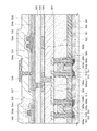
先の実施の形態に示す信号処理回路は、基準電圧生成回路101、分圧回路102、及びオペアンプ104を、シリコンなどを用いたトランジスタで形成され、これらの回路に積層して、保持回路106、保持回路107、及び保持回路108等を、酸化物半導体を用いたトランジスタで形成される。
In the signal processing circuit described in the above embodiment, the reference
図10には、本発明の一態様に係る信号処理回路の一部の断面を示す。図10に示す信号処理回路は、下部に第1の半導体材料(例えば、シリコン)を用いたn型のトランジスタ及びp型のトランジスタを有し、上部に第2の半導体材料(例えば、酸化物半導体)を用いたトランジスタ及び容量素子を有する。 FIG. 10 illustrates a partial cross section of a signal processing circuit according to one embodiment of the present invention. The signal processing circuit illustrated in FIG. 10 includes an n-type transistor and a p-type transistor using a first semiconductor material (for example, silicon) in a lower portion, and a second semiconductor material (for example, an oxide semiconductor) in an upper portion. ) And a capacitor.
〈下部のトランジスタの構成〉
n型のトランジスタ510は、半導体材料を含む基板500に設けられたチャネル形成領域501と、チャネル形成領域501を挟むように設けられた低濃度不純物領域502及び高濃度不純物領域503(これらを合わせて単に不純物領域とも呼ぶ)と、該不純物領域に接して設けられた金属間化合物領域507と、チャネル形成領域501上に設けられたゲート絶縁膜504aと、ゲート絶縁膜504a上に設けられたゲート電極層505aと、金属間化合物領域507と接して設けられたソース電極層506a及びドレイン電極層506bと、を有する。ゲート電極層505aの側面には、サイドウォール絶縁膜508aが設けられている。トランジスタ510を覆うように層間絶縁膜521及び層間絶縁膜522が設けられている。層間絶縁膜521及び層間絶縁膜522に形成された開口を通じて、ソース電極層506a及びドレイン電極層506bと、金属間化合物領域507とが接続されている。
<Configuration of lower transistor>
The n-
p型のトランジスタ520は、半導体材料を含む基板500に設けられたチャネル形成領域511と、チャネル形成領域511を挟むように設けられた低濃度不純物領域512及び高濃度不純物領域513(これらを合わせて単に不純物領域とも呼ぶ)と、該不純物領域に接して設けられた金属間化合物領域517と、チャネル形成領域511上に設けられたゲート絶縁膜504bと、ゲート絶縁膜504b上に設けられたゲート電極層505bと、金属間化合物領域517と接して設けられたソース電極層506c及びドレイン電極層506dと、を有する。ゲート電極層505bの側面には、サイドウォール絶縁膜508bが設けられている。トランジスタ520を覆うように層間絶縁膜521及び層間絶縁膜522が設けられている。層間絶縁膜521及び層間絶縁膜522に形成された開口を通じて、ソース電極層506c及びドレイン電極層506dと、金属間化合物領域517とが接続している。
A p-
また、基板500には、トランジスタ510と、トランジスタ520のそれぞれを囲むように素子分離絶縁膜509が設けられている。
In addition, an element
なお、図10では、トランジスタ510及びトランジスタ520が、半導体基板にチャネルが形成されるトランジスタである場合について示すが、トランジスタ510及びトランジスタ520が、絶縁表面上に形成された非晶質半導体膜、多結晶半導体膜にチャネルが形成されるトランジスタであってもよい。また、SOI基板のように、単結晶半導体膜にチャネルが形成されるトランジスタであってもよい。
Note that FIG. 10 illustrates the case where the
半導体基板として、単結晶半導体基板を用いることにより、トランジスタ510及びトランジスタ520を、高速動作させることができる。よって、先の実施の形態に示す信号処理回路における基準電圧生成回路、分圧回路、及びオペアンプ等を、単結晶半導体基板に形成することが好ましい。
By using a single crystal semiconductor substrate as the semiconductor substrate, the
また、トランジスタ510と、トランジスタ520とは、配線523によって、それぞれ接続されており、配線523上には、絶縁膜524が設けられている。また、絶縁膜524上には、導電層525a、525b、絶縁膜526が設けられている。絶縁膜526は、絶縁膜524上に、導電層525a、525bを形成した後、導電層525a、525b上に、絶縁膜を形成し、当該絶縁膜を、導電層525a、525bの上面が露出するまで、研磨処理を行ったものであることが好ましい。
In addition, the
〈上部のトランジスタの構成〉
上部のトランジスタ530は、シリコンよりもバンドギャップが広い半導体膜にチャネルが形成されるトランジスタである。トランジスタ530は、絶縁膜524上に設けられた導電層525bと、導電層525b上に設けられた絶縁膜531及び絶縁膜532と、絶縁膜532上に設けられた半導体膜533と、半導体膜533に接して設けられたソース電極層534a、ドレイン電極層534bと、半導体膜533、ソース電極層534a、ドレイン電極層534b上に設けられたゲート絶縁膜535と、ゲート絶縁膜535上に設けられたゲート電極層536aと、を有する。なお、導電層525bは、ゲート電極層として機能する。
<Configuration of upper transistor>
The
図10では、半導体膜を挟んで上下に2つのゲート電極層を有する場合について示している。一方のゲート電極層には、オン状態またはオフ状態を制御するための信号が与えられ、他方のゲート電極層は、電気的に絶縁しているフローティングの状態であっても良いし、電位が他から与えられている状態であっても良い。後者の場合、一対の電極に、同じ高さの電位が与えられていても良いし、他方のゲート電極層にのみ接地電位などの固定の電位が与えられていても良い。他方のゲート電極層に与える電位の高さを制御することで、トランジスタの閾値電圧を制御することができる。 FIG. 10 shows a case where two gate electrode layers are provided above and below a semiconductor film. One gate electrode layer is supplied with a signal for controlling an on state or an off state, and the other gate electrode layer may be in an electrically insulated floating state or may have a potential other than that. The state given by may be sufficient. In the latter case, the pair of electrodes may be given the same potential, or only the other gate electrode layer may be given a fixed potential such as a ground potential. By controlling the potential applied to the other gate electrode layer, the threshold voltage of the transistor can be controlled.
また、絶縁膜532上には、導電層534cが設けられ、導電層534c上には、ゲート絶縁膜535が設けられ、ゲート絶縁膜535上には、導電層536bが設けられている。導電層534c、ゲート絶縁膜535、導電層536bによって、容量素子540が構成される。
A
また、トランジスタ530及び容量素子540を覆うように、層間絶縁膜537、層間絶縁膜538が設けられている。また、層間絶縁膜537及び層間絶縁膜538に形成された開口を通じて、ソース電極層534aと、配線539とが接続されている。
Further, an
シリコンよりも広いバンドギャップを有する半導体膜としては化合物半導体があり、例えば、酸化物半導体、窒化物半導体などがある。本実施の形態では、半導体膜533として、酸化物半導体を用いる場合について説明する。
As a semiconductor film having a wider band gap than silicon, there is a compound semiconductor, such as an oxide semiconductor or a nitride semiconductor. In this embodiment, the case where an oxide semiconductor is used as the
トランジスタ530に用いる酸化物半導体は、電子供与体(ドナー)となる水分または水素などの不純物が低減され、なおかつ酸素欠損が低減されることにより、高純度化された酸化物半導体(purified Oxide Semiconductor)であることが好ましい。高純度化された酸化物半導体は、i型(真性半導体)又はi型に限りなく近い。そのため、上記酸化物半導体を用いたトランジスタは、オフ電流が著しく小さいという特性を有する。また、酸化物半導体のバンドギャップは、2eV以上、好ましくは2.5eV以上、より好ましくは3eV以上である。水分または水素などの不純物濃度が十分に低減され、なおかつ酸素欠損が低減されることにより高純度化された酸化物半導体膜を用いることにより、トランジスタのオフ電流を著しく小さくすることができる。
An oxide semiconductor used for the
具体的に、高純度化された酸化物半導体を半導体膜に用いたトランジスタのオフ電流が小さいことは、いろいろな実験により証明できる。例えば、チャネル幅が1×106μmでチャネル長が10μmの素子であっても、ソース端子とドレイン端子間の電圧(ドレイン電圧)が1Vから10Vの範囲において、オフ電流が、半導体パラメータアナライザの測定限界以下、すなわち1×10⁻¹³A以下という特性を得ることができる。この場合、オフ電流をトランジスタのチャネル幅で除した数値に相当するオフ電流密度は、100zA/μm以下であることが分かる。また、容量素子とトランジスタとを接続して、容量素子に流入または容量素子から流出する電荷を当該トランジスタで制御する回路を用いて、オフ電流密度の測定を行った。当該測定では、上記トランジスタに高純度化された酸化物半導体膜をチャネル形成領域に用い、容量素子の単位時間あたりの電荷量の推移から当該トランジスタのオフ電流密度を測定した。その結果、トランジスタのソース端子とドレイン端子間の電圧が3Vの場合に、数十yA/μmという、さらに低いオフ電流密度が得られることが分かった。従って、高純度化された酸化物半導体膜をチャネル形成領域に用いたトランジスタは、シリコンを用いたトランジスタに比べてオフ電流が著しく小さいといえる。 Specifically, it can be proved by various experiments that the off-state current of a transistor using a highly purified oxide semiconductor as a semiconductor film is small. For example, even in an element having a channel width of 1 × 10 6 μm and a channel length of 10 μm, the off-state current of the semiconductor parameter analyzer is reduced when the voltage between the source terminal and the drain terminal (drain voltage) is in the range of 1V to 10V. It is possible to obtain characteristics that are below the measurement limit, that is, 1 × 10 −13 A or less. In this case, it can be seen that the off-current density corresponding to a value obtained by dividing the off-current by the channel width of the transistor is 100 zA / μm or less. Further, off-state current density was measured using a circuit in which a capacitor and a transistor are connected and charge flowing into or out of the capacitor is controlled by the transistor. In this measurement, a highly purified oxide semiconductor film of the transistor was used for a channel formation region, and the off-state current density of the transistor was measured from the change in charge amount per unit time of the capacitor. As a result, it was found that when the voltage between the source terminal and the drain terminal of the transistor is 3 V, an even lower off-current density of several tens of yA / μm can be obtained. Therefore, a transistor using a highly purified oxide semiconductor film for a channel formation region can be said to have significantly smaller off-state current than a transistor using silicon.
また、酸化物半導体としては、少なくともインジウム(In)あるいは亜鉛(Zn)を含むことが好ましい。また、該酸化物半導体を用いたトランジスタの電気的特性のばらつきを減らすためのスタビライザーとして、それらに加えてガリウム(Ga)、スズ(Sn)、ハフニウム(Hf)、アルミニウム(Al)、ジルコニウム(Zr)のいずれか一種または複数種を含むことが好ましい。 The oxide semiconductor preferably contains at least indium (In) or zinc (Zn). Further, as a stabilizer for reducing variation in electrical characteristics of a transistor using the oxide semiconductor, in addition to them, gallium (Ga), tin (Sn), hafnium (Hf), aluminum (Al), zirconium (Zr It is preferable that any one type or multiple types of these are included.
また、他のスタビライザーとして、ランタノイドである、ランタン(La)、セリウム(Ce)、プラセオジム(Pr)、ネオジム(Nd)、サマリウム(Sm)、ユウロピウム(Eu)、ガドリニウム(Gd)、テルビウム(Tb)、ジスプロシウム(Dy)、ホルミウム(Ho)、エルビウム(Er)、ツリウム(Tm)、イッテルビウム(Yb)、ルテチウム(Lu)のいずれか一種または複数種を含んでいてもよい。 As other stabilizers, lanthanoids such as lanthanum (La), cerium (Ce), praseodymium (Pr), neodymium (Nd), samarium (Sm), europium (Eu), gadolinium (Gd), terbium (Tb) , Dysprosium (Dy), holmium (Ho), erbium (Er), thulium (Tm), ytterbium (Yb), or lutetium (Lu) may be included.
例えば、酸化物半導体として、酸化インジウム、酸化スズ、酸化亜鉛、二元系金属の酸化物であるIn−Zn系酸化物、Sn−Zn系酸化物、Al−Zn系酸化物、Zn−Mg系酸化物、Sn−Mg系酸化物、In−Mg系酸化物、In−Ga系酸化物、三元系金属の酸化物であるIn−Ga−Zn系酸化物(IGZOとも表記する)、In−Al−Zn系酸化物、In−Sn−Zn系酸化物、Sn−Ga−Zn系酸化物、Al−Ga−Zn系酸化物、Sn−Al−Zn系酸化物、In−Hf−Zn系酸化物、In−La−Zn系酸化物、In−Pr−Zn系酸化物、In−Nd−Zn系酸化物、In−Sm−Zn系酸化物、In−Eu−Zn系酸化物、In−Gd−Zn系酸化物、In−Tb−Zn系酸化物、In−Dy−Zn系酸化物、In−Ho−Zn系酸化物、In−Er−Zn系酸化物、In−Tm−Zn系酸化物、In−Yb−Zn系酸化物、In−Lu−Zn系酸化物、四元系金属の酸化物であるIn−Sn−Ga−Zn系酸化物、In−Hf−Ga−Zn系酸化物、In−Al−Ga−Zn系酸化物、In−Sn−Al−Zn系酸化物、In−Sn−Hf−Zn系酸化物、In−Hf−Al−Zn系酸化物を用いることができる。 For example, as an oxide semiconductor, indium oxide, tin oxide, zinc oxide, binary metal oxides such as In—Zn oxide, Sn—Zn oxide, Al—Zn oxide, Zn—Mg oxide Oxides, Sn—Mg oxides, In—Mg oxides, In—Ga oxides, In—Ga—Zn oxides (also referred to as IGZO) which are oxides of ternary metals, In— Al-Zn oxide, In-Sn-Zn oxide, Sn-Ga-Zn oxide, Al-Ga-Zn oxide, Sn-Al-Zn oxide, In-Hf-Zn oxide In-La-Zn-based oxide, In-Pr-Zn-based oxide, In-Nd-Zn-based oxide, In-Sm-Zn-based oxide, In-Eu-Zn-based oxide, In-Gd -Zn oxide, In-Tb-Zn oxide, In-Dy-Zn oxide, n-Ho-Zn-based oxide, In-Er-Zn-based oxide, In-Tm-Zn-based oxide, In-Yb-Zn-based oxide, In-Lu-Zn-based oxide, quaternary metal In—Sn—Ga—Zn-based oxide, In—Hf—Ga—Zn-based oxide, In—Al—Ga—Zn-based oxide, In—Sn—Al—Zn-based oxide, In— Sn-Hf-Zn-based oxides and In-Hf-Al-Zn-based oxides can be used.
なお、例えば、In−Ga−Zn系酸化物とは、InとGaとZnを含む酸化物という意味であり、InとGaとZnの比率は問わない。また、InとGaとZn以外の金属元素を含んでいてもよい。In−Ga−Zn系酸化物は、無電界時の抵抗が十分に高くオフ電流を十分に小さくすることが可能であり、また、移動度も高い。 Note that for example, an In—Ga—Zn-based oxide means an oxide containing In, Ga, and Zn, and there is no limitation on the ratio of In, Ga, and Zn. Moreover, metal elements other than In, Ga, and Zn may be included. An In—Ga—Zn-based oxide has sufficiently high resistance when no electric field is applied, and can sufficiently reduce off-state current. In addition, the In—Ga—Zn-based oxide has high mobility.
例えば、In:Ga:Zn=1:1:1(=1/3:1/3:1/3)あるいはIn:Ga:Zn=2:2:1(=2/5:2/5:1/5)の原子比のIn−Ga−Zn系酸化物やその組成の近傍の酸化物を用いることができる。あるいは、In:Sn:Zn=1:1:1(=1/3:1/3:1/3)、In:Sn:Zn=2:1:3(=1/3:1/6:1/2)あるいはIn:Sn:Zn=2:1:5(=1/4:1/8:5/8)の原子比のIn−Sn−Zn系酸化物やその組成の近傍の酸化物を用いるとよい。 For example, In: Ga: Zn = 1: 1: 1 (= 1/3: 1/3: 1/3) or In: Ga: Zn = 2: 2: 1 (= 2/5: 2/5: 1). / 5) atomic ratio In—Ga—Zn-based oxides and oxides in the vicinity of the composition can be used. Alternatively, In: Sn: Zn = 1: 1: 1 (= 1/3: 1/3: 1/3), In: Sn: Zn = 2: 1: 3 (= 1/3: 1/6: 1) / 2) or In: Sn: Zn = 2: 1: 5 (= 1/4: 1/8: 5/8) atomic ratio In—Sn—Zn-based oxide or an oxide in the vicinity of the composition. Use it.
例えば、In−Sn−Zn系酸化物では比較的容易に高い移動度が得られる。しかしながら、In−Ga−Zn系酸化物でも、バルク内欠陥密度を低減することにより移動度を上げることができる。 For example, high mobility can be obtained relatively easily with an In—Sn—Zn-based oxide. However, mobility can be increased by reducing the defect density in the bulk also in the case of using an In—Ga—Zn-based oxide.
酸化物半導体膜は、例えば非単結晶を有してもよい。非単結晶は、例えば、CAAC(C Axis Aligned Crystal)、多結晶、微結晶、非晶質部を有する。非晶質部は、微結晶、CAACよりも欠陥準位密度が高い。また、微結晶は、CAACよりも欠陥準位密度が高い。なお、CAACを有する酸化物半導体を、CAAC−OS(C Axis Aligned Crystalline Oxide Semiconductor)と呼ぶ。 For example, the oxide semiconductor film may include a non-single crystal. The non-single crystal includes, for example, CAAC (C Axis Aligned Crystal), polycrystal, microcrystal, and amorphous part. The amorphous part has a higher density of defect states than microcrystals and CAAC. In addition, microcrystals have a higher density of defect states than CAAC. Note that an oxide semiconductor including CAAC is referred to as a CAAC-OS (C Axis Crystallized Oxide Semiconductor).
酸化物半導体膜は、例えばCAAC−OSを有してもよい。CAAC−OSは、例えば、c軸配向し、a軸または/およびb軸はマクロに揃っていない。 For example, the oxide semiconductor film may include a CAAC-OS. For example, the CAAC-OS is c-axis oriented, and the a-axis and / or the b-axis are not aligned macroscopically.
酸化物半導体膜は、例えば微結晶を有してもよい。なお、微結晶を有する酸化物半導体を、微結晶酸化物半導体と呼ぶ。微結晶酸化物半導体膜は、例えば、1nm以上10nm未満のサイズの微結晶(ナノ結晶ともいう。)を膜中に含む。 The oxide semiconductor film may include microcrystal, for example. Note that an oxide semiconductor including microcrystal is referred to as a microcrystalline oxide semiconductor. The microcrystalline oxide semiconductor film includes microcrystal (also referred to as nanocrystal) with a size greater than or equal to 1 nm and less than 10 nm, for example.
酸化物半導体膜は、例えば非晶質部を有してもよい。なお、非晶質部を有する酸化物半導体を、非晶質酸化物半導体と呼ぶ。非晶質酸化物半導体膜は、例えば、原子配列が無秩序であり、結晶成分を有さない。または、非晶質酸化物半導体膜は、例えば、完全な非晶質であり、結晶部を有さない。 For example, the oxide semiconductor film may include an amorphous part. Note that an oxide semiconductor having an amorphous part is referred to as an amorphous oxide semiconductor. An amorphous oxide semiconductor film has, for example, disordered atomic arrangement and no crystal component. Alternatively, the amorphous oxide semiconductor film is, for example, completely amorphous and has no crystal part.
なお、酸化物半導体膜が、CAAC−OS、微結晶酸化物半導体、非晶質酸化物半導体の混合膜であってもよい。混合膜は、例えば、非晶質酸化物半導体の領域と、微結晶酸化物半導体の領域と、CAAC−OSの領域と、を有する。また、混合膜は、例えば、非晶質酸化物半導体の領域と、微結晶酸化物半導体の領域と、CAAC−OSの領域と、の積層構造を有してもよい。 Note that the oxide semiconductor film may be a mixed film of a CAAC-OS, a microcrystalline oxide semiconductor, and an amorphous oxide semiconductor. For example, the mixed film includes an amorphous oxide semiconductor region, a microcrystalline oxide semiconductor region, and a CAAC-OS region. The mixed film may have a stacked structure of an amorphous oxide semiconductor region, a microcrystalline oxide semiconductor region, and a CAAC-OS region, for example.
なお、酸化物半導体膜は、例えば、単結晶を有してもよい。 Note that the oxide semiconductor film may include a single crystal, for example.
酸化物半導体膜は、複数の結晶部を有し、当該結晶部のc軸が被形成面の法線ベクトルまたは表面の法線ベクトルに平行な方向に揃っていることが好ましい。なお、異なる結晶部間で、それぞれa軸およびb軸の向きが異なっていてもよい。そのような酸化物半導体膜の一例としては、CAAC−OS膜がある。 The oxide semiconductor film preferably includes a plurality of crystal parts, and the c-axis of the crystal parts is aligned in a direction parallel to the normal vector of the formation surface or the normal vector of the surface. Note that the directions of the a-axis and the b-axis may be different between different crystal parts. An example of such an oxide semiconductor film is a CAAC-OS film.
CAAC−OS膜に含まれる結晶部は、一辺が100nm未満の立方体内に収まる大きさであることが多い。また、透過型電子顕微鏡(TEM:Transmission Electron Microscope)による観察像では、CAAC−OS膜に含まれる結晶部と結晶部との境界は明確ではない。また、TEMによってCAAC−OS膜には明確な粒界(グレインバウンダリーともいう。)は確認できない。そのため、CAAC−OS膜は、粒界に起因する電子移動度の低下が抑制される。 In most cases, a crystal part included in the CAAC-OS film fits in a cube whose one side is less than 100 nm. Further, in the observation image obtained by a transmission electron microscope (TEM), the boundary between the crystal part and the crystal part included in the CAAC-OS film is not clear. In addition, a clear grain boundary (also referred to as a grain boundary) cannot be confirmed in the CAAC-OS film by TEM. Therefore, in the CAAC-OS film, reduction in electron mobility due to grain boundaries is suppressed.
CAAC−OS膜に含まれる結晶部は、例えば、c軸がCAAC−OS膜の被形成面の法線ベクトルまたは表面の法線ベクトルに平行な方向になるように揃い、かつab面に垂直な方向から見て金属原子が三角形状または六角形状に配列し、c軸に垂直な方向から見て金属原子が層状または金属原子と酸素原子とが層状に配列している。なお、異なる結晶部間で、それぞれa軸およびb軸の向きが異なっていてもよい。本明細書において、単に垂直と記載する場合、80°以上100°以下、好ましくは85°以上95°以下の範囲も含まれることとする。また、単に平行と記載する場合、−10°以上10°以下、好ましくは−5°以上5°以下の範囲も含まれることとする。 The crystal part included in the CAAC-OS film is aligned so that, for example, the c-axis is in a direction parallel to the normal vector of the formation surface of the CAAC-OS film or the normal vector of the surface, and is perpendicular to the ab plane. When viewed from the direction, the metal atoms are arranged in a triangular shape or a hexagonal shape, and when viewed from the direction perpendicular to the c-axis, the metal atoms are arranged in layers, or the metal atoms and oxygen atoms are arranged in layers. Note that the directions of the a-axis and the b-axis may be different between different crystal parts. In this specification, the term “perpendicular” includes a range of 80 ° to 100 °, preferably 85 ° to 95 °. In addition, a simple term “parallel” includes a range of −10 ° to 10 °, preferably −5 ° to 5 °.
なお、CAAC−OS膜において、結晶部の分布が一様でなくてもよい。例えば、CAAC−OS膜の形成過程において、酸化物半導体膜の表面側から結晶成長させる場合、被形成面の近傍に対し表面の近傍では結晶部の占める割合が高くなることがある。また、CAAC−OS膜へ不純物を添加することにより、当該不純物添加領域において結晶部の結晶性が低下することもある。 Note that the distribution of crystal parts in the CAAC-OS film is not necessarily uniform. For example, in the formation process of the CAAC-OS film, when crystal growth is performed from the surface side of the oxide semiconductor film, the ratio of crystal parts in the vicinity of the surface of the oxide semiconductor film is higher in the vicinity of the surface. Further, when an impurity is added to the CAAC-OS film, the crystallinity of a crystal part in the impurity-added region may be decreased.
CAAC−OS膜に含まれる結晶部のc軸は、CAAC−OS膜の被形成面の法線ベクトルまたは表面の法線ベクトルに平行な方向になるように揃うため、CAAC−OS膜の形状(被形成面の断面形状または表面の断面形状)によっては互いに異なる方向を向くことがある。また、結晶部は、成膜したとき、または成膜後に加熱処理などの結晶化処理を行ったときに形成される。従って、結晶部のc軸は、CAAC−OS膜が形成されたときの被形成面の法線ベクトルまたは表面の法線ベクトルに平行な方向になるように揃う。 Since the c-axis of the crystal part included in the CAAC-OS film is aligned in a direction parallel to the normal vector of the formation surface of the CAAC-OS film or the normal vector of the surface, the shape of the CAAC-OS film ( Depending on the cross-sectional shape of the surface to be formed or the cross-sectional shape of the surface, the directions may be different from each other. The crystal part is formed when a film is formed or when a crystallization process such as a heat treatment is performed after the film formation. Therefore, the c-axes of the crystal parts are aligned in a direction parallel to the normal vector of the surface where the CAAC-OS film is formed or the normal vector of the surface.
CAAC−OS膜を用いたトランジスタは、可視光や紫外光の照射による電気特性の変動が小さい。よって、当該トランジスタは、信頼性が高い。 In a transistor using a CAAC-OS film, change in electrical characteristics due to irradiation with visible light or ultraviolet light is small. Therefore, the transistor has high reliability.
また、トランジスタのしきい値電圧のシフト量は、一方のゲート絶縁膜および他方のゲート絶縁膜の材料が同じである場合には、膜厚比によって制御することが可能である。一方のゲート絶縁膜および他方のゲート絶縁膜の膜厚比が1:10の場合は、膜厚比が1:1の場合と比較して、トランジスタのしきい値電圧のシフト量が大きくなる傾向がある。 In addition, the shift amount of the threshold voltage of a transistor can be controlled by the film thickness ratio when the materials of one gate insulating film and the other gate insulating film are the same. When the film thickness ratio of one gate insulating film and the other gate insulating film is 1:10, the shift amount of the threshold voltage of the transistor tends to be larger than when the film thickness ratio is 1: 1. There is.
半導体膜533は、成膜前、成膜時、成膜後において、水素が含まれないようにすることが好ましい。例えば、半導体膜533の成膜時に、水素が極力含まれないように成膜する、及び半導体膜533の成膜後に脱水化または脱水素化のための加熱処理を行うことが好ましい。また、半導体膜533と接する絶縁膜の成膜時に、水素が極力含まれないように成膜する、及び絶縁膜の成膜後に脱水化または脱水素化のための加熱処理を行うことが好ましい。
It is preferable that the
さらに、絶縁膜531として、水素が透過することを防止する膜を用いることにより、下部のトランジスタや、絶縁膜524、層間絶縁膜522等に含まれる水素が、半導体膜533に到達することを防止することができる。水素が透過することを防止する膜として、窒化シリコン膜、酸化窒化シリコン膜、酸化アルミニウム膜、酸化窒化アルミニウム等を用いることが好ましい。また、層間絶縁膜537として、水素が透過することを防止する膜を用いることにより、層間絶縁膜538に含まれる水素が、半導体膜533に到達することを防止することができる。
Further, by using a film that prevents hydrogen from permeating as the insulating
また、半導体膜533に含まれる酸素欠損を低減するために、半導体膜533に酸素を供給する処理を行うことが好ましい。例えば、半導体膜533と、酸素が過剰に含まれる絶縁膜とを接して設け、加熱処理を行うことで、酸素が過剰に含まれる絶縁膜から半導体膜533に、酸素を供給することができる。半導体膜533に酸素が供給されることにより、半導体膜533に含まれる酸素欠損を低減することができる。また、半導体膜533に脱水化または脱水素化処理を行った後、半導体膜533に酸素を添加する処理を行っても良い。酸素を添加する処理としては、例えば、イオン注入法、イオンドーピング法、プラズマ処理等により、酸素ラジカル、オゾン、酸素原子、酸素イオン等を、半導体膜533に添加して行う。
Further, in order to reduce oxygen vacancies contained in the
このように、半導体膜533において、不純物や酸素欠損が低減されることにより、キャリアの発生を抑制することができる。キャリア密度が高まることを抑制することで、キャリア密度に起因して、トランジスタのしきい値電圧がマイナス方向にシフトしてしまうことを抑制することができる。そのため、トランジスタの他方のゲート電極に印加する電位によって、トランジスタのしきい値電圧を容易に制御することが可能となる。
In this manner, in the
本実施の形態は、他の実施の形態と適宜組み合わせて適用することができる。 This embodiment can be combined with any of the other embodiments as appropriate.
101 基準電圧生成回路
102 分圧回路
103 スイッチ
104 オペアンプ
105 バイアス回路
105a バイアス回路
105b バイアス回路
106 保持回路
107 保持回路
108 保持回路
109 バイアス回路
111 スイッチ
112 容量素子
113 スイッチ
114 容量素子
115 トランジスタ
116 トランジスタ
117 トランジスタ
118 トランジスタ
119 スイッチ
120 容量素子
121 トランジスタ
122 トランジスタ
131 トランジスタ
132 トランジスタ
133 トランジスタ
134 トランジスタ
135 抵抗素子
136 トランジスタ
137 抵抗素子
138 トランジスタ
139 トランジスタ
140 トランジスタ
141 トランジスタ
142 トランジスタ
143 トランジスタ
144 容量素子
145 トランジスタ
151 トランジスタ
156 トランジスタ
162 トランジスタ
163 抵抗素子
164 容量素子
165 トランジスタ
166 トランジスタ
167 トランジスタ
168 トランジスタ
169 トランジスタ
171 保持回路
172 トランジスタ
173 抵抗素子
174 抵抗素子
175 保持回路
176 スイッチ
177 抵抗素子
178 トランジスタ
179 トランジスタ
180 スイッチ
181 容量素子
182 スイッチ
183 容量素子
190 基準電圧生成回路
300 電源制御装置
301 メインスイッチ
302 サブスイッチ
303 データ処理装置
304 整流回路
305 AC/DCコンバータ
306 DC/DCコンバータ
307 容量素子
308 不揮発性メモリ
309 揮発性記憶部
310 不揮発性記憶部
311 センサ
500 基板
501 チャネル形成領域
502 低濃度不純物領域
503 高濃度不純物領域
504a ゲート絶縁膜
504b ゲート絶縁膜
505a ゲート電極層
505b ゲート電極層
506a ソース電極層
506b ドレイン電極層
506c ソース電極層
506d ドレイン電極層
507 金属間化合物領域
508a サイドウォール絶縁膜
508b サイドウォール絶縁膜
509 素子分離絶縁膜
510 トランジスタ
511 チャネル形成領域
512 低濃度不純物領域
513 高濃度不純物領域
517 金属間化合物領域
520 トランジスタ
521 層間絶縁膜
522 層間絶縁膜
523 配線
524 絶縁膜
525a 導電層
525b 導電層
526 絶縁膜
530 トランジスタ
531 絶縁膜
532 絶縁膜
533 半導体膜
534a ソース電極層
534b ドレイン電極層
534c 導電層
535 ゲート絶縁膜
536a ゲート電極層
536b 導電層
537 層間絶縁膜
538 層間絶縁膜
539 配線
540 容量素子
101 Reference Voltage Generation Circuit 102 Voltage Dividing Circuit 103 Switch 104 Operational Amplifier 105 Bias Circuit 105a Bias Circuit 105b Bias Circuit 106 Holding Circuit 107 Holding Circuit 108 Holding Circuit 109 Bias Circuit 111 Switch 112 Capacitance Element 113 Switch 114 Capacitance Element 115 Transistor 116 Transistor 117 Transistor 118 Transistor 119 Switch 120 Capacitor 121 Transistor 122 Transistor 131 Transistor 132 Transistor 133 Transistor 134 Transistor 135 Resistor 136 Transistor 137 Resistor 138 Transistor 139 Transistor 140 Transistor 141 Transistor 142 Transistor 143 Transistor 144 Capacitor 145 Transistor 151 Transistor 156 Transistor 162 Transistor 163 Resistance element 164 Capacitance element 165 Transistor 166 Transistor 167 Transistor 168 Transistor 169 Transistor 171 Holding circuit 172 Transistor 173 Resistance element 174 Resistance element 175 Holding circuit 176 Switch 177 Resistance element 178 Transistor 179 Transistor 180 Switch 181 Capacity element 182 Switch 183 Capacitance element 190 Reference voltage generation circuit 300 Power supply control device 301 Main switch 302 Sub switch 303 Data processing device 304 Rectifier circuit 305 AC / DC converter 306 DC / DC converter 307 Capacitance element 308 Non-volatile memory 309 Volatile storage unit 310 Non-volatile Memory 311 Sensor 500 Substrate 501 Channel formation region 5 2 Low-concentration impurity region 503 High-concentration impurity region 504a Gate insulating film 504b Gate insulating film 505a Gate electrode layer 505b Gate electrode layer 506a Source electrode layer 506b Drain electrode layer 506c Source electrode layer 506d Drain electrode layer 507 Intermetallic compound region 508a Side wall Insulating film 508b Side wall insulating film 509 Element isolation insulating film 510 Transistor 511 Channel formation region 512 Low concentration impurity region 513 High concentration impurity region 517 Intermetallic compound region 520 Transistor 521 Interlayer insulating film 522 Interlayer insulating film 523 Wiring 524 Insulating film 525a Conductive Layer 525b conductive layer 526 insulating film 530 transistor 531 insulating film 532 insulating film 533 semiconductor film 534a source electrode layer 534b drain electrode layer 534c conductive layer 535 gate G insulating film 536a Gate electrode layer 536b Conductive layer 537 Interlayer insulating film 538 Interlayer insulating film 539 Wiring 540 Capacitor
Claims (7)
第1のトランジスタと、
第2のトランジスタと、
第1の容量素子と、
第2の容量素子と、
第2の回路と、を有し、
前記第2の回路は、差動回路と、バイアス回路と、を有し、
前記第1の電位は、前記第1のトランジスタのソース又はドレインの一方に入力され、
前記第1のトランジスタのソース又はドレインの他方は、前記差動回路と電気的に接続され、
前記第1の容量素子は、前記第1のトランジスタのソース又はドレインの他方と電気的に接続され、
前記第2の電位は、前記第2のトランジスタのソース又はドレインの一方に入力され、
前記第2のトランジスタのソース又はドレインの他方は、前記バイアス回路と電気的に接続され、
前記第2の容量素子は、前記第2のトランジスタのソース又はドレインの他方と電気的に接続され、
前記第1のトランジスタのチャネル形成領域、及び、前記第2のトランジスタのチャネル形成領域は、酸化物半導体を有し、
前記第1の回路は、第3のトランジスタを有し、
前記差動回路は、第4のトランジスタを有し、
前記第3のトランジスタのチャネル形成領域、及び、前記第4のトランジスタのチャネル形成領域は、シリコンを有し、
前記第1のトランジスタを非導通状態とし、前記第2のトランジスタを非導通状態とした後、前記第1の回路は、前記第1のトランジスタのソース又はドレインの一方への前記第1の電位の供給と、前記第2のトランジスタのソース又はドレインの一方への前記第2の電位の供給と、を停止することができる機能を有する半導体装置であって、
前記第3のトランジスタの上方、及び、前記第4のトランジスタの上方に、第1の絶縁層が配置され、
前記第1の絶縁層の上方に、前記第1のトランジスタ、及び、前記第2のトランジスタが配置されることを特徴とする半導体装置。 A first circuit having a function of generating a first potential and a second potential in a period during which the power supply voltage is supplied;
A first transistor;
A second transistor;
A first capacitive element;
A second capacitive element;
A second circuit,
The second circuit includes a differential circuit and a bias circuit,
The first potential is input to one of a source and a drain of the first transistor;
The other of the source and the drain of the first transistor is electrically connected to the differential circuit;
The first capacitor is electrically connected to the other of the source and the drain of the first transistor;
The second potential is input to one of a source and a drain of the second transistor;
The other of the source and the drain of the second transistor is electrically connected to the bias circuit;
The second capacitor is electrically connected to the other of the source and the drain of the second transistor;
The channel formation region of the first transistor and the channel formation region of the second transistor include an oxide semiconductor ,
The first circuit includes a third transistor;
The differential circuit includes a fourth transistor,
The channel formation region of the third transistor and the channel formation region of the fourth transistor have silicon.
After the first transistor is turned off and the second transistor is turned off, the first circuit has the first potential applied to one of a source or a drain of the first transistor. A semiconductor device having a function capable of stopping supply and supply of the second potential to one of a source and a drain of the second transistor ,
A first insulating layer is disposed above the third transistor and above the fourth transistor;
The semiconductor device , wherein the first transistor and the second transistor are disposed above the first insulating layer .
第1のトランジスタと、A first transistor;
第2のトランジスタと、A second transistor;
第1の容量素子と、A first capacitive element;
第2の容量素子と、A second capacitive element;
第2の回路と、を有し、A second circuit,
前記第2の回路は、差動回路と、バイアス回路と、を有し、The second circuit includes a differential circuit and a bias circuit,
前記第1の電位は、前記第1のトランジスタのソース又はドレインの一方に入力され、The first potential is input to one of a source and a drain of the first transistor;
前記第1のトランジスタのソース又はドレインの他方は、前記第2の回路と電気的に接続され、The other of the source and the drain of the first transistor is electrically connected to the second circuit;
前記第1の容量素子は、前記第1のトランジスタのソース又はドレインの他方と電気的に接続され、The first capacitor is electrically connected to the other of the source and the drain of the first transistor;
前記第2の電位は、前記第2のトランジスタのソース又はドレインの一方に入力され、The second potential is input to one of a source and a drain of the second transistor;
前記第2のトランジスタのソース又はドレインの他方は、前記第2の回路と電気的に接続され、The other of the source and the drain of the second transistor is electrically connected to the second circuit;
前記第2の容量素子は、前記第2のトランジスタのソース又はドレインの他方と電気的に接続され、The second capacitor is electrically connected to the other of the source and the drain of the second transistor;
前記第1のトランジスタのチャネル形成領域、及び、前記第2のトランジスタのチャネル形成領域は、酸化物半導体を有し、The channel formation region of the first transistor and the channel formation region of the second transistor include an oxide semiconductor,
前記第1の回路は、第3のトランジスタを有し、The first circuit includes a third transistor;
前記差動回路は、第4のトランジスタを有し、The differential circuit includes a fourth transistor,
前記第3のトランジスタのチャネル形成領域、及び、前記第4のトランジスタのチャネル形成領域は、シリコンを有し、The channel formation region of the third transistor and the channel formation region of the fourth transistor have silicon.
前記第1のトランジスタを非導通状態とし、前記第2のトランジスタを非導通状態とした後、前記第1の回路は、前記第1のトランジスタのソース又はドレインの一方への前記第1の電位の供給と、前記第2のトランジスタのソース又はドレインの一方への前記第2の電位の供給と、を停止することができる機能を有する半導体装置であって、After the first transistor is turned off and the second transistor is turned off, the first circuit has the first potential applied to one of a source or a drain of the first transistor. A semiconductor device having a function capable of stopping supply and supply of the second potential to one of a source and a drain of the second transistor,
前記第3のトランジスタの上方、及び、前記第4のトランジスタの上方に、第1の絶縁層が配置され、A first insulating layer is disposed above the third transistor and above the fourth transistor;
前記第1の絶縁層の上方に、前記第1のトランジスタ、及び、前記第2のトランジスタが配置されることを特徴とする半導体装置。The semiconductor device, wherein the first transistor and the second transistor are disposed above the first insulating layer.
第1のトランジスタと、
第2のトランジスタと、
第1の容量素子と、
第2の容量素子と、
第2の回路と、を有し、
前記第2の回路は、差動回路と、バイアス回路と、カレントミラー回路と、を有し、
前記第1の電位は、前記第1のトランジスタのソース又はドレインの一方に入力され、
前記第1のトランジスタのソース又はドレインの他方は、前記差動回路と電気的に接続され、
前記第1の容量素子は、前記第1のトランジスタのソース又はドレインの他方と電気的に接続され、
前記第2の電位は、前記第2のトランジスタのソース又はドレインの一方に入力され、
前記第2のトランジスタのソース又はドレインの他方は、前記バイアス回路と電気的に接続され、
前記第2の容量素子は、前記第2のトランジスタのソース又はドレインの他方と電気的に接続され、
前記第1のトランジスタのチャネル形成領域、及び、前記第2のトランジスタのチャネル形成領域は、酸化物半導体を有し、
前記第1の回路は、第3のトランジスタを有し、
前記差動回路は、第4のトランジスタを有し、
前記カレントミラー回路は、第5のトランジスタを有し、
前記第3のトランジスタのチャネル形成領域、前記第4のトランジスタのチャネル形成領域、及び、前記第5のトランジスタのチャネル形成領域は、シリコンを有し、
前記第1のトランジスタを非導通状態とし、前記第2のトランジスタを非導通状態とした後、前記第1の回路は、前記第1のトランジスタのソース又はドレインの一方への前記第1の電位の供給と、前記第2のトランジスタのソース又はドレインの一方への前記第2の電位の供給と、を停止することができる機能を有する半導体装置であって、
前記第3のトランジスタの上方、前記第4のトランジスタの上方、及び、前記第5のトランジスタの上方に、第1の絶縁層が配置され、
前記第1の絶縁層の上方に、前記第1のトランジスタ、及び、前記第2のトランジスタが配置されることを特徴とする半導体装置。 A first circuit having a function of generating a first potential and a second potential in a period during which the power supply voltage is supplied;
A first transistor;
A second transistor;
A first capacitive element;
A second capacitive element;
A second circuit,
The second circuit includes a differential circuit, a bias circuit, and a current mirror circuit,
The first potential is input to one of a source and a drain of the first transistor;
The other of the source and the drain of the first transistor is electrically connected to the differential circuit;
The first capacitor is electrically connected to the other of the source and the drain of the first transistor;
The second potential is input to one of a source and a drain of the second transistor;
The other of the source and the drain of the second transistor is electrically connected to the bias circuit;
The second capacitor is electrically connected to the other of the source and the drain of the second transistor;
The channel formation region of the first transistor and the channel formation region of the second transistor include an oxide semiconductor ,
The first circuit includes a third transistor;
The differential circuit includes a fourth transistor,
The current mirror circuit includes a fifth transistor,
The channel formation region of the third transistor, the channel formation region of the fourth transistor, and the channel formation region of the fifth transistor have silicon,
After the first transistor is turned off and the second transistor is turned off, the first circuit has the first potential applied to one of a source or a drain of the first transistor. A semiconductor device having a function capable of stopping supply and supply of the second potential to one of a source and a drain of the second transistor ,
A first insulating layer is disposed above the third transistor, above the fourth transistor, and above the fifth transistor;
The semiconductor device , wherein the first transistor and the second transistor are disposed above the first insulating layer .
第1のトランジスタと、A first transistor;
第2のトランジスタと、A second transistor;
第1の容量素子と、A first capacitive element;
第2の容量素子と、A second capacitive element;
第2の回路と、を有し、A second circuit,
前記第2の回路は、差動回路と、バイアス回路と、カレントミラー回路と、を有し、The second circuit includes a differential circuit, a bias circuit, and a current mirror circuit,
前記第1の電位は、前記第1のトランジスタのソース又はドレインの一方に入力され、The first potential is input to one of a source and a drain of the first transistor;
前記第1のトランジスタのソース又はドレインの他方は、前記第2の回路と電気的に接続され、The other of the source and the drain of the first transistor is electrically connected to the second circuit;
前記第1の容量素子は、前記第1のトランジスタのソース又はドレインの他方と電気的に接続され、The first capacitor is electrically connected to the other of the source and the drain of the first transistor;
前記第2の電位は、前記第2のトランジスタのソース又はドレインの一方に入力され、The second potential is input to one of a source and a drain of the second transistor;
前記第2のトランジスタのソース又はドレインの他方は、前記第2の回路と電気的に接続され、The other of the source and the drain of the second transistor is electrically connected to the second circuit;
前記第2の容量素子は、前記第2のトランジスタのソース又はドレインの他方と電気的に接続され、The second capacitor is electrically connected to the other of the source and the drain of the second transistor;
前記第1のトランジスタのチャネル形成領域、及び、前記第2のトランジスタのチャネル形成領域は、酸化物半導体を有し、The channel formation region of the first transistor and the channel formation region of the second transistor include an oxide semiconductor,
前記第1の回路は、第3のトランジスタを有し、The first circuit includes a third transistor;
前記差動回路は、第4のトランジスタを有し、The differential circuit includes a fourth transistor,
前記カレントミラー回路は、第5のトランジスタを有し、The current mirror circuit includes a fifth transistor,
前記第3のトランジスタのチャネル形成領域、前記第4のトランジスタのチャネル形成領域、及び、前記第5のトランジスタのチャネル形成領域は、シリコンを有し、The channel formation region of the third transistor, the channel formation region of the fourth transistor, and the channel formation region of the fifth transistor have silicon,
前記第1のトランジスタを非導通状態とし、前記第2のトランジスタを非導通状態とした後、前記第1の回路は、前記第1のトランジスタのソース又はドレインの一方への前記第1の電位の供給と、前記第2のトランジスタのソース又はドレインの一方への前記第2の電位の供給と、を停止することができる機能を有する半導体装置であって、After the first transistor is turned off and the second transistor is turned off, the first circuit has the first potential applied to one of a source or a drain of the first transistor. A semiconductor device having a function capable of stopping supply and supply of the second potential to one of a source and a drain of the second transistor,
前記第3のトランジスタの上方、前記第4のトランジスタの上方、及び、前記第5のトランジスタの上方に、第1の絶縁層が配置され、A first insulating layer is disposed above the third transistor, above the fourth transistor, and above the fifth transistor;
前記第1の絶縁層の上方に、前記第1のトランジスタ、及び、前記第2のトランジスタが配置されることを特徴とする半導体装置。The semiconductor device, wherein the first transistor and the second transistor are disposed above the first insulating layer.
第1のトランジスタと、A first transistor;
第2のトランジスタと、A second transistor;
第1の容量素子と、A first capacitive element;
第2の容量素子と、A second capacitive element;
第2の回路と、を有し、A second circuit,
前記第1の電位は、前記第1のトランジスタのソース又はドレインの一方に入力され、The first potential is input to one of a source and a drain of the first transistor;
前記第1のトランジスタのソース又はドレインの他方は、前記第2の回路と電気的に接続され、The other of the source and the drain of the first transistor is electrically connected to the second circuit;
前記第1の容量素子は、前記第1のトランジスタのソース又はドレインの他方と電気的に接続され、The first capacitor is electrically connected to the other of the source and the drain of the first transistor;
前記第2の電位は、前記第2のトランジスタのソース又はドレインの一方に入力され、The second potential is input to one of a source and a drain of the second transistor;
前記第2のトランジスタのソース又はドレインの他方は、前記第2の回路と電気的に接続され、The other of the source and the drain of the second transistor is electrically connected to the second circuit;
前記第2の容量素子は、前記第2のトランジスタのソース又はドレインの他方と電気的に接続され、The second capacitor is electrically connected to the other of the source and the drain of the second transistor;
前記第1のトランジスタのチャネル形成領域、及び、前記第2のトランジスタのチャネル形成領域は、酸化物半導体を有し、The channel formation region of the first transistor and the channel formation region of the second transistor include an oxide semiconductor,
前記第1の回路は、第3のトランジスタを有し、The first circuit includes a third transistor;
前記第2の回路は、第4のトランジスタを有し、The second circuit includes a fourth transistor;
前記第3のトランジスタのチャネル形成領域、及び、前記第4のトランジスタのチャネル形成領域は、シリコンを有し、The channel formation region of the third transistor and the channel formation region of the fourth transistor have silicon.
前記第1のトランジスタを非導通状態とし、前記第2のトランジスタを非導通状態とした後、前記第1の回路は、前記第1のトランジスタのソース又はドレインの一方への前記第1の電位の供給と、前記第2のトランジスタのソース又はドレインの一方への前記第2の電位の供給と、を停止することができる機能を有する半導体装置であって、After the first transistor is turned off and the second transistor is turned off, the first circuit has the first potential applied to one of a source or a drain of the first transistor. A semiconductor device having a function capable of stopping supply and supply of the second potential to one of a source and a drain of the second transistor,
前記第3のトランジスタの上方、及び、前記第4のトランジスタの上方に、第1の絶縁層が配置され、A first insulating layer is disposed above the third transistor and above the fourth transistor;
前記第1の絶縁層の上方に、前記第1のトランジスタ、及び、前記第2のトランジスタが配置されることを特徴とする半導体装置。The semiconductor device, wherein the first transistor and the second transistor are disposed above the first insulating layer.
前記第1のトランジスタは、第1のゲートと、第2のゲートと、を有し、The first transistor has a first gate and a second gate;
前記第2のトランジスタは、第3のゲートと、第4のゲートと、を有し、The second transistor has a third gate and a fourth gate,
前記第1の絶縁層の上方に、前記第1のゲート、及び、前記第3のゲートが配置され、The first gate and the third gate are disposed above the first insulating layer,
前記第1のゲートの上方、及び、前記第3のゲートの上方に、第2の絶縁層が配置され、A second insulating layer is disposed above the first gate and above the third gate;
前記第2の絶縁層の上方に、前記第1のトランジスタのチャネル形成領域、及び、前記第2のトランジスタのチャネル形成領域が配置され、A channel formation region of the first transistor and a channel formation region of the second transistor are disposed above the second insulating layer;
前記第1のトランジスタのチャネル形成領域の上方に、前記第2のゲートが配置され、The second gate is disposed above the channel formation region of the first transistor,
前記第2のトランジスタのチャネル形成領域の上方に、前記第4のゲートが配置され、The fourth gate is disposed above the channel formation region of the second transistor,
前記第2の絶縁層は、酸化アルミニウム膜を有することを特徴とする半導体装置。The semiconductor device, wherein the second insulating layer includes an aluminum oxide film.
前記第1のトランジスタと、前記第2のトランジスタとは、同じ信号で導通状態又は非導通状態が制御されていることを特徴とする半導体装置。The semiconductor device, wherein the first transistor and the second transistor are controlled to be in a conductive state or a non-conductive state by the same signal.
Priority Applications (1)
| Application Number | Priority Date | Filing Date | Title |
|---|---|---|---|
| JP2013047516A JP5975907B2 (en) | 2012-04-11 | 2013-03-11 | Semiconductor device |
Applications Claiming Priority (3)
| Application Number | Priority Date | Filing Date | Title |
|---|---|---|---|
| JP2012090058 | 2012-04-11 | ||
| JP2012090058 | 2012-04-11 | ||
| JP2013047516A JP5975907B2 (en) | 2012-04-11 | 2013-03-11 | Semiconductor device |
Related Child Applications (1)
| Application Number | Title | Priority Date | Filing Date |
|---|---|---|---|
| JP2016141101A Division JP2016219028A (en) | 2012-04-11 | 2016-07-19 | Semiconductor device |
Publications (3)
| Publication Number | Publication Date |
|---|---|
| JP2013235564A JP2013235564A (en) | 2013-11-21 |
| JP2013235564A5 JP2013235564A5 (en) | 2015-02-19 |
| JP5975907B2 true JP5975907B2 (en) | 2016-08-23 |
Family
ID=49232387
Family Applications (6)
| Application Number | Title | Priority Date | Filing Date |
|---|---|---|---|
| JP2013047516A Active JP5975907B2 (en) | 2012-04-11 | 2013-03-11 | Semiconductor device |
| JP2016141101A Withdrawn JP2016219028A (en) | 2012-04-11 | 2016-07-19 | Semiconductor device |
| JP2018039368A Active JP6636073B2 (en) | 2012-04-11 | 2018-03-06 | Semiconductor device |
| JP2019227042A Active JP6938604B2 (en) | 2012-04-11 | 2019-12-17 | Semiconductor device |
| JP2020067574A Withdrawn JP2020109707A (en) | 2012-04-11 | 2020-04-03 | Semiconductor device |
| JP2022075577A Withdrawn JP2022103243A (en) | 2012-04-11 | 2022-04-29 | Semiconductor device |
Family Applications After (5)
| Application Number | Title | Priority Date | Filing Date |
|---|---|---|---|
| JP2016141101A Withdrawn JP2016219028A (en) | 2012-04-11 | 2016-07-19 | Semiconductor device |
| JP2018039368A Active JP6636073B2 (en) | 2012-04-11 | 2018-03-06 | Semiconductor device |
| JP2019227042A Active JP6938604B2 (en) | 2012-04-11 | 2019-12-17 | Semiconductor device |
| JP2020067574A Withdrawn JP2020109707A (en) | 2012-04-11 | 2020-04-03 | Semiconductor device |
| JP2022075577A Withdrawn JP2022103243A (en) | 2012-04-11 | 2022-04-29 | Semiconductor device |
Country Status (4)
| Country | Link |
|---|---|
| US (3) | US9742356B2 (en) |
| JP (6) | JP5975907B2 (en) |
| KR (3) | KR20130115131A (en) |
| DE (1) | DE102013206284B4 (en) |
Families Citing this family (25)
| Publication number | Priority date | Publication date | Assignee | Title |
|---|---|---|---|---|
| JP5981157B2 (en) | 2012-02-09 | 2016-08-31 | 株式会社半導体エネルギー研究所 | Semiconductor device |
| JP5975907B2 (en) * | 2012-04-11 | 2016-08-23 | 株式会社半導体エネルギー研究所 | Semiconductor device |
| JP6243136B2 (en) | 2012-05-02 | 2017-12-06 | 株式会社半導体エネルギー研究所 | Switching converter |
| TWI641208B (en) | 2013-07-26 | 2018-11-11 | 日商半導體能源研究所股份有限公司 | Dcdc converter |
| JP6460592B2 (en) | 2013-07-31 | 2019-01-30 | 株式会社半導体エネルギー研究所 | DC-DC converter and semiconductor device |
| US9378844B2 (en) | 2013-07-31 | 2016-06-28 | Semiconductor Energy Laboratory Co., Ltd. | Semiconductor device including transistor whose gate is electrically connected to capacitor |
| US9343288B2 (en) | 2013-07-31 | 2016-05-17 | Semiconductor Energy Laboratory Co., Ltd. | Semiconductor device |
| US9374048B2 (en) * | 2013-08-20 | 2016-06-21 | Semiconductor Energy Laboratory Co., Ltd. | Signal processing device, and driving method and program thereof |
| KR102267237B1 (en) | 2014-03-07 | 2021-06-18 | 가부시키가이샤 한도오따이 에네루기 켄큐쇼 | Semiconductor device and electronic device |
| US10359794B2 (en) * | 2014-10-13 | 2019-07-23 | Qorvo Us, Inc. | Switched capacitor biasing circuit |
| US20170063112A1 (en) * | 2015-08-31 | 2017-03-02 | Semiconductor Energy Laboratory Co., Ltd. | Power storage device with monitoring ic |
| WO2017103731A1 (en) * | 2015-12-18 | 2017-06-22 | Semiconductor Energy Laboratory Co., Ltd. | Semiconductor device and display device including the same |
| TWI739796B (en) * | 2016-02-12 | 2021-09-21 | 日商半導體能源硏究所股份有限公司 | Semiconductor device and electronic device, and semiconductor wafer |
| JP6906978B2 (en) | 2016-02-25 | 2021-07-21 | 株式会社半導体エネルギー研究所 | Semiconductor devices, semiconductor wafers, and electronics |
| KR102605008B1 (en) | 2018-01-24 | 2023-11-24 | 가부시키가이샤 한도오따이 에네루기 켄큐쇼 | Semiconductor devices, electronic components, and electronic devices |
| US11817698B2 (en) | 2018-07-06 | 2023-11-14 | Semiconductor Energy Laboratory Co., Ltd. | Battery management circuit, power storage device, and electric device |
| US11531362B2 (en) | 2018-08-10 | 2022-12-20 | Semiconductor Energy Laboratory Co., Ltd. | Amplifier circuit, latch circuit, and sensing device |
| WO2020044168A1 (en) * | 2018-08-31 | 2020-03-05 | 株式会社半導体エネルギー研究所 | Semiconductor device and semiconductor device operation method |
| DE112019005072T5 (en) * | 2018-10-11 | 2021-07-22 | Semiconductor Energy Laboratory Co., Ltd. | Vehicle alarm device |
| KR20210080425A (en) * | 2018-10-25 | 2021-06-30 | 가부시키가이샤 한도오따이 에네루기 켄큐쇼 | Power storage device and how the power storage device works |
| US11899478B2 (en) | 2018-12-21 | 2024-02-13 | Semiconductor Energy Laboratory Co., Ltd. | Semiconductor device, electronic device, and artificial satellite |
| WO2020240331A1 (en) | 2019-05-31 | 2020-12-03 | 株式会社半導体エネルギー研究所 | Semiconductor device and wireless communication device including said semiconductor device |
| US20220231644A1 (en) * | 2019-06-07 | 2022-07-21 | Semiconductor Energy Laboratory Co., Ltd. | Semiconductor device |
| JPWO2021009591A1 (en) | 2019-07-12 | 2021-01-21 | ||
| US11243244B2 (en) * | 2019-10-10 | 2022-02-08 | Infineon Technologies Ag | Switched bypass capacitor for component characterization |
Family Cites Families (129)
| Publication number | Priority date | Publication date | Assignee | Title |
|---|---|---|---|---|
| JPS5539412A (en) | 1978-09-13 | 1980-03-19 | Hitachi Ltd | Insulating gate field effect transistor integrated circuit and its manufacture |
| US5159260A (en) | 1978-03-08 | 1992-10-27 | Hitachi, Ltd. | Reference voltage generator device |
| US4553098A (en) | 1978-04-05 | 1985-11-12 | Hitachi, Ltd. | Battery checker |
| US4559694A (en) | 1978-09-13 | 1985-12-24 | Hitachi, Ltd. | Method of manufacturing a reference voltage generator device |
| JPS60198861A (en) | 1984-03-23 | 1985-10-08 | Fujitsu Ltd | Thin film transistor |
| JPH0244256B2 (en) | 1987-01-28 | 1990-10-03 | Kagaku Gijutsucho Mukizaishitsu Kenkyushocho | INGAZN2O5DESHIMESARERUROTSUHOSHOKEINOSOJOKOZOOJUSURUKAGOBUTSUOYOBISONOSEIZOHO |
| JPH0244258B2 (en) | 1987-02-24 | 1990-10-03 | Kagaku Gijutsucho Mukizaishitsu Kenkyushocho | INGAZN3O6DESHIMESARERUROTSUHOSHOKEINOSOJOKOZOOJUSURUKAGOBUTSUOYOBISONOSEIZOHO |
| JPH0244260B2 (en) | 1987-02-24 | 1990-10-03 | Kagaku Gijutsucho Mukizaishitsu Kenkyushocho | INGAZN5O8DESHIMESARERUROTSUHOSHOKEINOSOJOKOZOOJUSURUKAGOBUTSUOYOBISONOSEIZOHO |
| JPS63210023A (en) | 1987-02-24 | 1988-08-31 | Natl Inst For Res In Inorg Mater | Compound having laminar structure of hexagonal crystal system expressed by ingazn4o7 and its production |
| JPH0244262B2 (en) | 1987-02-27 | 1990-10-03 | Kagaku Gijutsucho Mukizaishitsu Kenkyushocho | INGAZN6O9DESHIMESARERUROTSUHOSHOKEINOSOJOKOZOOJUSURUKAGOBUTSUOYOBISONOSEIZOHO |
| JPH0244263B2 (en) | 1987-04-22 | 1990-10-03 | Kagaku Gijutsucho Mukizaishitsu Kenkyushocho | INGAZN7O10DESHIMESARERUROTSUHOSHOKEINOSOJOKOZOOJUSURUKAGOBUTSUOYOBISONOSEIZOHO |
| JPH05251705A (en) | 1992-03-04 | 1993-09-28 | Fuji Xerox Co Ltd | Thin-film transistor |
| JPH06242847A (en) * | 1992-12-24 | 1994-09-02 | Hitachi Ltd | Reference voltage generating circuit |
| KR940017214A (en) | 1992-12-24 | 1994-07-26 | 가나이 쓰토무 | Reference voltage generator |
| JP3479375B2 (en) | 1995-03-27 | 2003-12-15 | 科学技術振興事業団 | Metal oxide semiconductor device in which a pn junction is formed with a thin film transistor made of a metal oxide semiconductor such as cuprous oxide, and methods for manufacturing the same |
| EP0820644B1 (en) | 1995-08-03 | 2005-08-24 | Koninklijke Philips Electronics N.V. | Semiconductor device provided with transparent switching element |
| JP3550450B2 (en) * | 1995-09-01 | 2004-08-04 | 株式会社日立製作所 | Semiconductor device |
| JP3625598B2 (en) | 1995-12-30 | 2005-03-02 | 三星電子株式会社 | Manufacturing method of liquid crystal display device |
| JP4170454B2 (en) | 1998-07-24 | 2008-10-22 | Hoya株式会社 | Article having transparent conductive oxide thin film and method for producing the same |
| JP2000150861A (en) | 1998-11-16 | 2000-05-30 | Tdk Corp | Oxide thin film |
| JP3276930B2 (en) | 1998-11-17 | 2002-04-22 | 科学技術振興事業団 | Transistor and semiconductor device |
| US6114907A (en) | 1998-12-08 | 2000-09-05 | National Semiconductor Corporation | Amplifier with dynamic compensation and method |
| TW460731B (en) | 1999-09-03 | 2001-10-21 | Ind Tech Res Inst | Electrode structure and production method of wide viewing angle LCD |
| JP4089858B2 (en) | 2000-09-01 | 2008-05-28 | 国立大学法人東北大学 | Semiconductor device |
| KR20020038482A (en) | 2000-11-15 | 2002-05-23 | 모리시타 요이찌 | Thin film transistor array, method for producing the same, and display panel using the same |
| JP3997731B2 (en) | 2001-03-19 | 2007-10-24 | 富士ゼロックス株式会社 | Method for forming a crystalline semiconductor thin film on a substrate |
| JP2002289859A (en) | 2001-03-23 | 2002-10-04 | Minolta Co Ltd | Thin-film transistor |
| JP3925839B2 (en) | 2001-09-10 | 2007-06-06 | シャープ株式会社 | Semiconductor memory device and test method thereof |
| JP4090716B2 (en) | 2001-09-10 | 2008-05-28 | 雅司 川崎 | Thin film transistor and matrix display device |
| JP4164562B2 (en) | 2002-09-11 | 2008-10-15 | 独立行政法人科学技術振興機構 | Transparent thin film field effect transistor using homologous thin film as active layer |
| WO2003040441A1 (en) | 2001-11-05 | 2003-05-15 | Japan Science And Technology Agency | Natural superlattice homologous single crystal thin film, method for preparation thereof, and device using said single crystal thin film |
| JP2003283271A (en) * | 2002-01-17 | 2003-10-03 | Semiconductor Energy Lab Co Ltd | Electric circuit |
| JP3866579B2 (en) * | 2002-01-25 | 2007-01-10 | 富士フイルムホールディングス株式会社 | Thin metal film |
| JP4083486B2 (en) | 2002-02-21 | 2008-04-30 | 独立行政法人科学技術振興機構 | Method for producing LnCuO (S, Se, Te) single crystal thin film |
| US7049190B2 (en) | 2002-03-15 | 2006-05-23 | Sanyo Electric Co., Ltd. | Method for forming ZnO film, method for forming ZnO semiconductor layer, method for fabricating semiconductor device, and semiconductor device |
| JP3933591B2 (en) | 2002-03-26 | 2007-06-20 | 淳二 城戸 | Organic electroluminescent device |
| US7339187B2 (en) | 2002-05-21 | 2008-03-04 | State Of Oregon Acting By And Through The Oregon State Board Of Higher Education On Behalf Of Oregon State University | Transistor structures |
| JP2004022625A (en) | 2002-06-13 | 2004-01-22 | Murata Mfg Co Ltd | Manufacturing method of semiconductor device and its manufacturing method |
| US7105868B2 (en) | 2002-06-24 | 2006-09-12 | Cermet, Inc. | High-electron mobility transistor with zinc oxide |
| US7067843B2 (en) | 2002-10-11 | 2006-06-27 | E. I. Du Pont De Nemours And Company | Transparent oxide semiconductor thin film transistors |
| JP4166105B2 (en) | 2003-03-06 | 2008-10-15 | シャープ株式会社 | Semiconductor device and manufacturing method thereof |
| JP2004273732A (en) | 2003-03-07 | 2004-09-30 | Sharp Corp | Active matrix substrate and its producing process |
| JP4108633B2 (en) | 2003-06-20 | 2008-06-25 | シャープ株式会社 | THIN FILM TRANSISTOR, MANUFACTURING METHOD THEREOF, AND ELECTRONIC DEVICE |
| US7262463B2 (en) | 2003-07-25 | 2007-08-28 | Hewlett-Packard Development Company, L.P. | Transistor including a deposited channel region having a doped portion |
| JP4445780B2 (en) * | 2004-03-02 | 2010-04-07 | Okiセミコンダクタ株式会社 | Voltage regulator |
| US7282782B2 (en) | 2004-03-12 | 2007-10-16 | Hewlett-Packard Development Company, L.P. | Combined binary oxide semiconductor device |
| US7145174B2 (en) | 2004-03-12 | 2006-12-05 | Hewlett-Packard Development Company, Lp. | Semiconductor device |
| KR101078483B1 (en) | 2004-03-12 | 2011-10-31 | 도꾸리쯔교세이호징 가가꾸 기쥬쯔 신꼬 기꼬 | Switching device of lcd or organic electro luminescence display |
| US7297977B2 (en) | 2004-03-12 | 2007-11-20 | Hewlett-Packard Development Company, L.P. | Semiconductor device |
| US7531852B2 (en) * | 2004-06-14 | 2009-05-12 | Denso Corporation | Electronic unit with a substrate where an electronic circuit is fabricated |
| US7211825B2 (en) | 2004-06-14 | 2007-05-01 | Yi-Chi Shih | Indium oxide-based thin film transistors and circuits |
| JP2006100760A (en) | 2004-09-02 | 2006-04-13 | Casio Comput Co Ltd | Thin-film transistor and its manufacturing method |
| US7285501B2 (en) | 2004-09-17 | 2007-10-23 | Hewlett-Packard Development Company, L.P. | Method of forming a solution processed device |
| US7298084B2 (en) | 2004-11-02 | 2007-11-20 | 3M Innovative Properties Company | Methods and displays utilizing integrated zinc oxide row and column drivers in conjunction with organic light emitting diodes |
| US7863611B2 (en) | 2004-11-10 | 2011-01-04 | Canon Kabushiki Kaisha | Integrated circuits utilizing amorphous oxides |
| US7453065B2 (en) | 2004-11-10 | 2008-11-18 | Canon Kabushiki Kaisha | Sensor and image pickup device |
| EP2455975B1 (en) | 2004-11-10 | 2015-10-28 | Canon Kabushiki Kaisha | Field effect transistor with amorphous oxide |
| US7868326B2 (en) | 2004-11-10 | 2011-01-11 | Canon Kabushiki Kaisha | Field effect transistor |
| EP1810335B1 (en) | 2004-11-10 | 2020-05-27 | Canon Kabushiki Kaisha | Light-emitting device |
| US7791072B2 (en) | 2004-11-10 | 2010-09-07 | Canon Kabushiki Kaisha | Display |
| US7829444B2 (en) | 2004-11-10 | 2010-11-09 | Canon Kabushiki Kaisha | Field effect transistor manufacturing method |
| US7579224B2 (en) | 2005-01-21 | 2009-08-25 | Semiconductor Energy Laboratory Co., Ltd. | Method for manufacturing a thin film semiconductor device |
| TWI412138B (en) | 2005-01-28 | 2013-10-11 | Semiconductor Energy Lab | Semiconductor device, electronic device, and method of manufacturing semiconductor device |
| TWI445178B (en) | 2005-01-28 | 2014-07-11 | Semiconductor Energy Lab | Semiconductor device, electronic device, and method of manufacturing semiconductor device |
| US7858451B2 (en) | 2005-02-03 | 2010-12-28 | Semiconductor Energy Laboratory Co., Ltd. | Electronic device, semiconductor device and manufacturing method thereof |
| US7948171B2 (en) | 2005-02-18 | 2011-05-24 | Semiconductor Energy Laboratory Co., Ltd. | Light emitting device |
| US20060197092A1 (en) | 2005-03-03 | 2006-09-07 | Randy Hoffman | System and method for forming conductive material on a substrate |
| US8681077B2 (en) | 2005-03-18 | 2014-03-25 | Semiconductor Energy Laboratory Co., Ltd. | Semiconductor device, and display device, driving method and electronic apparatus thereof |
| WO2006105077A2 (en) | 2005-03-28 | 2006-10-05 | Massachusetts Institute Of Technology | Low voltage thin film transistor with high-k dielectric material |
| US7645478B2 (en) | 2005-03-31 | 2010-01-12 | 3M Innovative Properties Company | Methods of making displays |
| US8300031B2 (en) | 2005-04-20 | 2012-10-30 | Semiconductor Energy Laboratory Co., Ltd. | Semiconductor device comprising transistor having gate and drain connected through a current-voltage conversion element |
| JP2006344849A (en) | 2005-06-10 | 2006-12-21 | Casio Comput Co Ltd | Thin film transistor |
| US7402506B2 (en) | 2005-06-16 | 2008-07-22 | Eastman Kodak Company | Methods of making thin film transistors comprising zinc-oxide-based semiconductor materials and transistors made thereby |
| US7691666B2 (en) | 2005-06-16 | 2010-04-06 | Eastman Kodak Company | Methods of making thin film transistors comprising zinc-oxide-based semiconductor materials and transistors made thereby |
| US7507618B2 (en) | 2005-06-27 | 2009-03-24 | 3M Innovative Properties Company | Method for making electronic devices using metal oxide nanoparticles |
| KR100711890B1 (en) | 2005-07-28 | 2007-04-25 | 삼성에스디아이 주식회사 | Organic Light Emitting Display and Fabrication Method for the same |
| JP2007059128A (en) | 2005-08-23 | 2007-03-08 | Canon Inc | Organic electroluminescent display device and manufacturing method thereof |
| JP4850457B2 (en) | 2005-09-06 | 2012-01-11 | キヤノン株式会社 | Thin film transistor and thin film diode |
| JP2007073705A (en) | 2005-09-06 | 2007-03-22 | Canon Inc | Oxide-semiconductor channel film transistor and its method of manufacturing same |
| JP4280736B2 (en) | 2005-09-06 | 2009-06-17 | キヤノン株式会社 | Semiconductor element |
| JP5116225B2 (en) | 2005-09-06 | 2013-01-09 | キヤノン株式会社 | Manufacturing method of oxide semiconductor device |
| US20110106614A1 (en) * | 2005-11-01 | 2011-05-05 | Jumptap, Inc. | Mobile User Characteristics Influenced Search Results |
| EP3614442A3 (en) | 2005-09-29 | 2020-03-25 | Semiconductor Energy Laboratory Co., Ltd. | Semiconductor device having oxide semiconductor layer and manufactoring method thereof |
| JP5037808B2 (en) | 2005-10-20 | 2012-10-03 | キヤノン株式会社 | Field effect transistor using amorphous oxide, and display device using the transistor |
| CN101707212B (en) | 2005-11-15 | 2012-07-11 | 株式会社半导体能源研究所 | Semiconductor device and method of manufacturing the |
| TWI292281B (en) | 2005-12-29 | 2008-01-01 | Ind Tech Res Inst | Pixel structure of active organic light emitting diode and method of fabricating the same |
| US7867636B2 (en) | 2006-01-11 | 2011-01-11 | Murata Manufacturing Co., Ltd. | Transparent conductive film and method for manufacturing the same |
| JP4977478B2 (en) | 2006-01-21 | 2012-07-18 | 三星電子株式会社 | ZnO film and method of manufacturing TFT using the same |
| US7576394B2 (en) | 2006-02-02 | 2009-08-18 | Kochi Industrial Promotion Center | Thin film transistor including low resistance conductive thin films and manufacturing method thereof |
| US7977169B2 (en) | 2006-02-15 | 2011-07-12 | Kochi Industrial Promotion Center | Semiconductor device including active layer made of zinc oxide with controlled orientations and manufacturing method thereof |
| JP4804975B2 (en) * | 2006-03-22 | 2011-11-02 | エルピーダメモリ株式会社 | Reference potential generating circuit and semiconductor memory device having the same |
| KR20070101595A (en) | 2006-04-11 | 2007-10-17 | 삼성전자주식회사 | Zno thin film transistor |
| US20070252928A1 (en) | 2006-04-28 | 2007-11-01 | Toppan Printing Co., Ltd. | Structure, transmission type liquid crystal display, reflection type display and manufacturing method thereof |
| JP4912037B2 (en) * | 2006-05-29 | 2012-04-04 | ルネサスエレクトロニクス株式会社 | Semiconductor integrated circuit device |
| JP5028033B2 (en) | 2006-06-13 | 2012-09-19 | キヤノン株式会社 | Oxide semiconductor film dry etching method |
| JP4999400B2 (en) | 2006-08-09 | 2012-08-15 | キヤノン株式会社 | Oxide semiconductor film dry etching method |
| JP4609797B2 (en) | 2006-08-09 | 2011-01-12 | Nec液晶テクノロジー株式会社 | Thin film device and manufacturing method thereof |
| JP4332545B2 (en) | 2006-09-15 | 2009-09-16 | キヤノン株式会社 | Field effect transistor and manufacturing method thereof |
| JP4274219B2 (en) | 2006-09-27 | 2009-06-03 | セイコーエプソン株式会社 | Electronic devices, organic electroluminescence devices, organic thin film semiconductor devices |
| JP5164357B2 (en) | 2006-09-27 | 2013-03-21 | キヤノン株式会社 | Semiconductor device and manufacturing method of semiconductor device |
| US7622371B2 (en) | 2006-10-10 | 2009-11-24 | Hewlett-Packard Development Company, L.P. | Fused nanocrystal thin film semiconductor and method |
| US7772021B2 (en) | 2006-11-29 | 2010-08-10 | Samsung Electronics Co., Ltd. | Flat panel displays comprising a thin-film transistor having a semiconductive oxide in its channel and methods of fabricating the same for use in flat panel displays |
| JP2008140684A (en) | 2006-12-04 | 2008-06-19 | Toppan Printing Co Ltd | Color el display, and its manufacturing method |
| JP4906093B2 (en) | 2006-12-27 | 2012-03-28 | 株式会社半導体エネルギー研究所 | Semiconductor device |
| KR101303578B1 (en) | 2007-01-05 | 2013-09-09 | 삼성전자주식회사 | Etching method of thin film |
| US8207063B2 (en) | 2007-01-26 | 2012-06-26 | Eastman Kodak Company | Process for atomic layer deposition |
| KR100851215B1 (en) | 2007-03-14 | 2008-08-07 | 삼성에스디아이 주식회사 | Thin film transistor and organic light-emitting dislplay device having the thin film transistor |
| US7795613B2 (en) | 2007-04-17 | 2010-09-14 | Toppan Printing Co., Ltd. | Structure with transistor |
| KR101325053B1 (en) | 2007-04-18 | 2013-11-05 | 삼성디스플레이 주식회사 | Thin film transistor substrate and manufacturing method thereof |
| KR20080094300A (en) | 2007-04-19 | 2008-10-23 | 삼성전자주식회사 | Thin film transistor and method of manufacturing the same and flat panel display comprising the same |
| KR101334181B1 (en) | 2007-04-20 | 2013-11-28 | 삼성전자주식회사 | Thin Film Transistor having selectively crystallized channel layer and method of manufacturing the same |
| CN101663762B (en) | 2007-04-25 | 2011-09-21 | 佳能株式会社 | Oxynitride semiconductor |
| KR101345376B1 (en) | 2007-05-29 | 2013-12-24 | 삼성전자주식회사 | Fabrication method of ZnO family Thin film transistor |
| CN101878460A (en) * | 2007-11-30 | 2010-11-03 | Nxp股份有限公司 | Arrangement and approach for providing a reference voltage |
| JP5215158B2 (en) | 2007-12-17 | 2013-06-19 | 富士フイルム株式会社 | Inorganic crystalline alignment film, method for manufacturing the same, and semiconductor device |
| JP2009171548A (en) | 2007-12-20 | 2009-07-30 | Nec Electronics Corp | Differential amplifier circuit |
| JP5326628B2 (en) | 2008-03-03 | 2013-10-30 | 富士通株式会社 | Electronic circuit equipment |
| JP4623179B2 (en) | 2008-09-18 | 2011-02-02 | ソニー株式会社 | Thin film transistor and manufacturing method thereof |
| KR101628013B1 (en) | 2008-10-02 | 2016-06-21 | 가부시키가이샤 한도오따이 에네루기 켄큐쇼 | Semiconductor device and rfid tag using the semiconductor device |
| JP5451280B2 (en) | 2008-10-09 | 2014-03-26 | キヤノン株式会社 | Wurtzite crystal growth substrate, manufacturing method thereof, and semiconductor device |
| KR101585958B1 (en) | 2008-12-29 | 2016-01-18 | 주식회사 동부하이텍 | Reference voltage generation circuit |
| JP5467845B2 (en) * | 2009-09-29 | 2014-04-09 | セイコーインスツル株式会社 | Voltage regulator |
| KR101829309B1 (en) * | 2010-01-22 | 2018-02-19 | 가부시키가이샤 한도오따이 에네루기 켄큐쇼 | Semiconductor device |
| US8508276B2 (en) * | 2010-08-25 | 2013-08-13 | Semiconductor Energy Laboratory Co., Ltd. | Semiconductor device including latch circuit |
| JP5727892B2 (en) | 2010-08-26 | 2015-06-03 | 株式会社半導体エネルギー研究所 | Semiconductor device |
| JP5674107B2 (en) | 2010-10-19 | 2015-02-25 | 日本電気株式会社 | Communication system, control device, processing rule setting method and program |
| JP5908263B2 (en) * | 2010-12-03 | 2016-04-26 | 株式会社半導体エネルギー研究所 | DC-DC converter |
| US8542066B2 (en) * | 2012-02-09 | 2013-09-24 | Analog Devices, Inc. | Apparatus and methods for reducing output noise of a signal channel |
| JP5975907B2 (en) * | 2012-04-11 | 2016-08-23 | 株式会社半導体エネルギー研究所 | Semiconductor device |
-
2013
- 2013-03-11 JP JP2013047516A patent/JP5975907B2/en active Active
- 2013-03-14 US US13/802,945 patent/US9742356B2/en active Active
- 2013-04-01 KR KR1020130034960A patent/KR20130115131A/en active Application Filing
- 2013-04-10 DE DE102013206284.2A patent/DE102013206284B4/en active Active
-
2016
- 2016-07-19 JP JP2016141101A patent/JP2016219028A/en not_active Withdrawn
-
2017
- 2017-08-17 US US15/679,203 patent/US10560056B2/en not_active Expired - Fee Related
-
2018
- 2018-03-06 JP JP2018039368A patent/JP6636073B2/en active Active
-
2019
- 2019-12-17 JP JP2019227042A patent/JP6938604B2/en active Active
-
2020
- 2020-02-06 US US16/783,306 patent/US11316478B2/en active Active
- 2020-03-17 KR KR1020200032655A patent/KR102127089B1/en active Application Filing
- 2020-04-03 JP JP2020067574A patent/JP2020109707A/en not_active Withdrawn
- 2020-06-17 KR KR1020200073489A patent/KR102243974B1/en active IP Right Grant
-
2022
- 2022-04-29 JP JP2022075577A patent/JP2022103243A/en not_active Withdrawn
Also Published As
| Publication number | Publication date |
|---|---|
| KR20130115131A (en) | 2013-10-21 |
| JP2016219028A (en) | 2016-12-22 |
| KR20200033246A (en) | 2020-03-27 |
| US20180102741A1 (en) | 2018-04-12 |
| KR102127089B1 (en) | 2020-06-25 |
| US9742356B2 (en) | 2017-08-22 |
| JP6938604B2 (en) | 2021-09-22 |
| JP2020109707A (en) | 2020-07-16 |
| JP2020057421A (en) | 2020-04-09 |
| US11316478B2 (en) | 2022-04-26 |
| KR20200074075A (en) | 2020-06-24 |
| DE102013206284A1 (en) | 2013-10-17 |
| JP2022103243A (en) | 2022-07-07 |
| US20130271220A1 (en) | 2013-10-17 |
| KR102243974B1 (en) | 2021-04-22 |
| US20200177132A1 (en) | 2020-06-04 |
| JP2013235564A (en) | 2013-11-21 |
| DE102013206284B4 (en) | 2023-07-06 |
| US10560056B2 (en) | 2020-02-11 |
| JP6636073B2 (en) | 2020-01-29 |
| JP2018092668A (en) | 2018-06-14 |
Similar Documents
| Publication | Publication Date | Title |
|---|---|---|
| KR102127089B1 (en) | Semiconductor device | |
| US9304523B2 (en) | Power supply circuit and method for driving the same | |
| JP6240693B2 (en) | DCDC converter | |
| JP6184155B2 (en) | Power circuit | |
| US8711594B2 (en) | Asymmetric switching rectifier | |
| JP6676575B2 (en) | Semiconductor device | |
| US9058892B2 (en) | Semiconductor device and shift register | |
| JP2018038051A (en) | Control circuit | |
| TWI641208B (en) | Dcdc converter | |
| US20130307496A1 (en) | Semiconductor device and driving method thereof | |
| JP6391743B2 (en) | Power supply system | |
| US20150035573A1 (en) | Semiconductor device | |
| KR20140044818A (en) | Semiconductor device |
Legal Events
| Date | Code | Title | Description |
|---|---|---|---|
| A521 | Request for written amendment filed |
Free format text: JAPANESE INTERMEDIATE CODE: A523 Effective date: 20141219 |
|
| A621 | Written request for application examination |
Free format text: JAPANESE INTERMEDIATE CODE: A621 Effective date: 20141219 |
|
| A977 | Report on retrieval |
Free format text: JAPANESE INTERMEDIATE CODE: A971007 Effective date: 20151127 |
|
| A131 | Notification of reasons for refusal |
Free format text: JAPANESE INTERMEDIATE CODE: A131 Effective date: 20151201 |
|
| A521 | Request for written amendment filed |
Free format text: JAPANESE INTERMEDIATE CODE: A523 Effective date: 20160115 |
|
| TRDD | Decision of grant or rejection written | ||
| A01 | Written decision to grant a patent or to grant a registration (utility model) |
Free format text: JAPANESE INTERMEDIATE CODE: A01 Effective date: 20160628 |
|
| A61 | First payment of annual fees (during grant procedure) |
Free format text: JAPANESE INTERMEDIATE CODE: A61 Effective date: 20160719 |
|
| R150 | Certificate of patent or registration of utility model |
Ref document number: 5975907 Country of ref document: JP Free format text: JAPANESE INTERMEDIATE CODE: R150 |
|
| R250 | Receipt of annual fees |
Free format text: JAPANESE INTERMEDIATE CODE: R250 |
|
| R250 | Receipt of annual fees |
Free format text: JAPANESE INTERMEDIATE CODE: R250 |
|
| R250 | Receipt of annual fees |
Free format text: JAPANESE INTERMEDIATE CODE: R250 |
|
| R250 | Receipt of annual fees |
Free format text: JAPANESE INTERMEDIATE CODE: R250 |
|
| R250 | Receipt of annual fees |
Free format text: JAPANESE INTERMEDIATE CODE: R250 |