JP2013229013A - Array controller and storage system - Google Patents
Array controller and storage system Download PDFInfo
- Publication number
- JP2013229013A JP2013229013A JP2013049821A JP2013049821A JP2013229013A JP 2013229013 A JP2013229013 A JP 2013229013A JP 2013049821 A JP2013049821 A JP 2013049821A JP 2013049821 A JP2013049821 A JP 2013049821A JP 2013229013 A JP2013229013 A JP 2013229013A
- Authority
- JP
- Japan
- Prior art keywords
- insulating layer
- oxide semiconductor
- layer
- transistor
- oxide
- Prior art date
- Legal status (The legal status is an assumption and is not a legal conclusion. Google has not performed a legal analysis and makes no representation as to the accuracy of the status listed.)
- Withdrawn
Links
Images


Classifications
-
- G—PHYSICS
- G06—COMPUTING; CALCULATING OR COUNTING
- G06F—ELECTRIC DIGITAL DATA PROCESSING
- G06F12/00—Accessing, addressing or allocating within memory systems or architectures
- G06F12/02—Addressing or allocation; Relocation
- G06F12/08—Addressing or allocation; Relocation in hierarchically structured memory systems, e.g. virtual memory systems
- G06F12/0802—Addressing of a memory level in which the access to the desired data or data block requires associative addressing means, e.g. caches
- G06F12/0866—Addressing of a memory level in which the access to the desired data or data block requires associative addressing means, e.g. caches for peripheral storage systems, e.g. disk cache
-
- G—PHYSICS
- G06—COMPUTING; CALCULATING OR COUNTING
- G06F—ELECTRIC DIGITAL DATA PROCESSING
- G06F12/00—Accessing, addressing or allocating within memory systems or architectures
- G06F12/02—Addressing or allocation; Relocation
- G06F12/08—Addressing or allocation; Relocation in hierarchically structured memory systems, e.g. virtual memory systems
- G06F12/0802—Addressing of a memory level in which the access to the desired data or data block requires associative addressing means, e.g. caches
- G06F12/0893—Caches characterised by their organisation or structure
-
- G—PHYSICS
- G06—COMPUTING; CALCULATING OR COUNTING
- G06F—ELECTRIC DIGITAL DATA PROCESSING
- G06F2212/00—Indexing scheme relating to accessing, addressing or allocation within memory systems or architectures
- G06F2212/22—Employing cache memory using specific memory technology
- G06F2212/222—Non-volatile memory
-
- Y—GENERAL TAGGING OF NEW TECHNOLOGICAL DEVELOPMENTS; GENERAL TAGGING OF CROSS-SECTIONAL TECHNOLOGIES SPANNING OVER SEVERAL SECTIONS OF THE IPC; TECHNICAL SUBJECTS COVERED BY FORMER USPC CROSS-REFERENCE ART COLLECTIONS [XRACs] AND DIGESTS
- Y02—TECHNOLOGIES OR APPLICATIONS FOR MITIGATION OR ADAPTATION AGAINST CLIMATE CHANGE
- Y02D—CLIMATE CHANGE MITIGATION TECHNOLOGIES IN INFORMATION AND COMMUNICATION TECHNOLOGIES [ICT], I.E. INFORMATION AND COMMUNICATION TECHNOLOGIES AIMING AT THE REDUCTION OF THEIR OWN ENERGY USE
- Y02D10/00—Energy efficient computing, e.g. low power processors, power management or thermal management
Abstract
Description
本発明は、物、方法、または、製造方法に関する。または、本発明は、プロセス、マシン、マニュファクチャ、または、組成物(コンポジション・オブ・マター)に関する。特に、本発明は、例えば、半導体装置、表示装置、発光装置、それらの駆動方法、または、それらの作製方法に関する。特に、本発明は、アレイコントローラ及びストレージシステムに関する。 The present invention relates to an object, a method, or a manufacturing method. Or this invention relates to a process, a machine, a manufacture, or a composition (composition of matter). In particular, the present invention relates to, for example, a semiconductor device, a display device, a light-emitting device, a driving method thereof, or a manufacturing method thereof. In particular, the present invention relates to an array controller and a storage system.
近年、ハードディスク(Hard Disk Drive(HDD))などの大容量の記憶デバイスを複数用いたストレージシステムが広く使用されている。一般的に、ストレージシステムには、複数の記憶デバイスと、これらの記憶デバイスに対するアクセスを制御するアレイコントローラとが含まれる。 In recent years, a storage system using a plurality of large-capacity storage devices such as a hard disk (Hard Disk Drive (HDD)) has been widely used. Generally, a storage system includes a plurality of storage devices and an array controller that controls access to these storage devices.
このような大容量の記憶デバイスを用いたストレージシステムとして、JBOD(Just A Bunch Of Disks)システムや、RAID(Redundant Array Of Inexpensive Disks、又は、Redundant Array Of Independent Disks)システムが挙げられる。 As a storage system using such a large-capacity storage device, a JBOD (Just A Bunch Of Disks) system, a RAID (Redundant Array Of Independent Disks, or a Redundant Array Of Independent Disks) system can be cited.
高い信頼性を求められるストレージシステムは、停電等によるシステム停止の際のデータの整合性確保のため、キャッシュシステムを搭載している(特許文献1、特許文献2、特許文献3、及び特許文献4参照)。
A storage system that requires high reliability is equipped with a cache system to ensure data consistency when the system is stopped due to a power failure or the like (
停電等によるシステム停止の際のデータの整合性確保と保護は、ストレージの信頼性と可用性(アベイラビリティ(Availability)ともいう。システムが継続して稼動できる能力)を高める重要な要素である。例えば、システム停止時に書き込み完了前のデータを、高速なキャッシュシステムに記憶(バックアップ)させることによって、システム回復時(システム再起動時)にキャッシュシステムに記憶させたデータを読み出し、システム停止時の不整合の状態を解消できる。 Ensuring data integrity and protection in the event of a system stop due to a power failure or the like is an important factor for improving storage reliability and availability (also referred to as availability, the ability of the system to continue to operate). For example, by storing (backup) the data before completion of writing in the high-speed cache system when the system is stopped, the data stored in the cache system is read when the system is recovered (when the system is restarted). The consistency state can be eliminated.
このようなキャッシュシステムの例として、具体的には、キャッシュメモリとしてDRAM(Dynamic Random Access Memory)等の揮発性メモリを用い、キャッシュメモリ用の蓄電装置を用いるシステムが挙げられる。DRAMは、記憶素子を構成するトランジスタを選択してキャパシタ(容量素子)に電荷を蓄積することで、情報(データ)を記憶する。DRAMでは、電力の供給がなくなると記憶内容が失われるので、停電時の電源確保のためキャッシュメモリ用の蓄電装置が必要となる。 As an example of such a cache system, specifically, there is a system that uses a volatile memory such as a DRAM (Dynamic Random Access Memory) as a cache memory and uses a power storage device for the cache memory. A DRAM stores information (data) by selecting a transistor constituting a storage element and accumulating electric charge in a capacitor (capacitance element). In the DRAM, the stored contents are lost when the power supply is lost, so a power storage device for a cache memory is required to secure a power supply during a power failure.
また、DRAMと蓄電装置を用いる代わりに、キャッシュシステムとしてフラッシュメモリ等の不揮発性メモリを用いて、停電時のデータの整合性確保及び保護を行うことも可能である。 Further, instead of using a DRAM and a power storage device, it is possible to secure and protect data consistency during a power failure by using a nonvolatile memory such as a flash memory as a cache system.
フラッシュメモリは、トランジスタのゲート電極とチャネル形成領域との間にフローティングゲートを有し、当該フローティングゲートに電荷を保持させることで記憶を行うため、データの保持期間は極めて長く(半永久的)、揮発性メモリで必要なリフレッシュ動作が不要であるという利点を有している。 A flash memory has a floating gate between a gate electrode of a transistor and a channel formation region, and stores data by holding electric charge in the floating gate. Therefore, a data holding period is extremely long (semi-permanent) and volatile This has the advantage that the refresh operation necessary for the memory is unnecessary.
しかしながら、DRAMと蓄電装置を用いるキャッシュシステムでは、蓄電装置の交換のために、ストレージシステムの停止が必要である。そのため、このようなストレージシステムの停止を伴う蓄電装置の交換は、ストレージシステムの可用性を低下させる恐れがある。 However, in a cache system using a DRAM and a power storage device, it is necessary to stop the storage system in order to replace the power storage device. For this reason, such replacement of the power storage device that accompanies the suspension of the storage system may reduce the availability of the storage system.
また、DRAMを用いたキャッシュシステムにおいては、記憶素子を構成するトランジスタにリーク電流が存在し、トランジスタが選択されていない状態(オフ状態ともいう)でもキャパシタから電荷が流出、または流入するため、データの保持期間が短い。このため、所定の周期で再度の書き込み動作(リフレッシュ動作)が必要であり、消費電力を十分に低減することは困難である。 In a cache system using a DRAM, a leakage current exists in a transistor included in a memory element, and charge flows out or flows in from a capacitor even when the transistor is not selected (also referred to as an off state). The retention period is short. For this reason, a re-writing operation (refresh operation) is necessary at a predetermined cycle, and it is difficult to sufficiently reduce power consumption.
また、フラッシュメモリを用いたキャッシュシステムにおいては、書き込みの際に生じるトンネル電流によって記憶素子を構成するゲート絶縁層が劣化するため、所定回数の書き込みによって記憶素子が機能しなくなるという問題が生じる。つまり、フラッシュメモリの書き込み回数には上限値が存在する。 In addition, in a cache system using a flash memory, the gate insulating layer constituting the memory element deteriorates due to a tunnel current generated at the time of writing, so that there is a problem that the memory element does not function after a predetermined number of writes. That is, there is an upper limit for the number of times the flash memory is written.
この問題の影響を緩和するために、例えば、各記憶素子の書き込み回数を均一化する手法が採られるが、これを実現するためには、複雑な周辺回路が必要になってしまう。そして、このような手法を採用しても、根本的な寿命の問題が解消するわけではない。つまり、フラッシュメモリは、ストレージシステムのような情報の書き換え頻度が高い用途には不向きである。 In order to alleviate the influence of this problem, for example, a method of making the number of writings of each storage element uniform is adopted, but in order to realize this, a complicated peripheral circuit is required. And even if such a method is adopted, the fundamental problem of lifetime is not solved. That is, the flash memory is not suitable for an application with a high information rewriting frequency such as a storage system.
また、フローティングゲートに電荷を注入させるため、または、その電荷を除去するためには、高い電圧が必要であり、また、そのための回路も必要である。さらに、電荷の注入、または除去の動作には比較的長い時間を要し、書き込み、消去の高速化が容易ではないという問題もある。 Further, in order to inject charge into the floating gate or to remove the charge, a high voltage is required, and a circuit therefor is also necessary. Furthermore, there is a problem that the charge injection or removal operation takes a relatively long time and it is not easy to speed up writing and erasing.
以上を鑑みて、開示される発明の一態様では、蓄電装置の交換が不要なキャッシュメモリを有するストレージシステムを提供することを課題の一とする。 In view of the above, an object of one embodiment of the disclosed invention is to provide a storage system including a cache memory that does not require replacement of a power storage device.
または、開示される発明の一態様では、消費電力が小さいキャッシュメモリを有するストレージシステムを提供することを課題の一とする。 Another object of one embodiment of the disclosed invention is to provide a storage system including a cache memory with low power consumption.
または、開示される発明の一態様では、書き換え回数に制限のないキャッシュメモリを有するストレージシステムを提供することを課題の一とする。 Another object of one embodiment of the disclosed invention is to provide a storage system including a cache memory with no limit on the number of rewrites.
なお、これらの課題の記載は、他の課題の存在を妨げるものではない。なお、本発明の一態様は、これらの課題の全てを解決する必要はないものとする。なお、これら以外の課題は、明細書、図面、請求項などの記載から、自ずと明らかとなるものであり、明細書、図面、請求項などの記載から、これら以外の課題を抽出することが可能である。 Note that the description of these problems does not disturb the existence of other problems. Note that one embodiment of the present invention does not have to solve all of these problems. Issues other than these will be apparent from the description of the specification, drawings, claims, etc., and other issues can be extracted from the descriptions of the specification, drawings, claims, etc. It is.
開示される発明の一態様は、酸化物半導体を有するトランジスタ(以下「酸化物半導体トランジスタ」という)を用いた記憶装置をキャッシュメモリとして有するストレージシステムを提供する。 One embodiment of the disclosed invention provides a storage system including a memory device including a transistor including an oxide semiconductor (hereinafter referred to as an “oxide semiconductor transistor”) as a cache memory.
酸化物半導体トランジスタは、オフ状態のソース及びドレイン間のチャネル幅1μmあたりのリーク電流(以下「オフ電流」という)が、使用時の温度(例えば、25℃)で100zA(1×10⁻¹⁹A)以下、好ましくは10zA(1×10⁻²⁰A)以下、さらに好ましくは、1zA(1×10⁻²¹A)以下である。なお、より具体的には、オフ電流とは、オフ状態のとき、たとえばソース電位を基準としたときのゲート電位との電位差がしきい値電圧以下のときのドレイン電流とする。 An oxide semiconductor transistor has a leakage current per channel width of 1 μm between an off-state source and drain (hereinafter referred to as “off-current”) of 100 zA (1 × 10 −19 A) at a temperature during use (for example, 25 ° C.). ) Or less, preferably 10 zA (1 × 10 −20 A) or less, more preferably 1 zA (1 × 10 −21 A) or less. More specifically, the off-state current is a drain current when the potential difference from the gate potential with respect to the source potential is equal to or lower than the threshold voltage in the off-state, for example.
上述のように、酸化物半導体トランジスタは、オフ電流が極めて小さいという特徴を有している。このため、酸化物半導体トランジスタをオフ状態とすることで、酸化物半導体トランジスタのソースまたはドレインの一方と電気的に接続されたノードの電荷を長時間にわたって保持することが可能となる。このようなオフ電流がきわめて小さい酸化物半導体トランジスタを用いた記憶回路が、ノードの電荷をデータとして保持すれば、当該記憶回路は当該データを長時間にわたって保持可能な記憶回路となる。別言すれば、このようなオフ電流がきわめて小さい酸化物半導体トランジスタを用いた記憶回路は、実用的には不揮発性の記憶装置(メモリ)であるといえる。 As described above, an oxide semiconductor transistor has a feature that an off-state current is extremely small. Therefore, when the oxide semiconductor transistor is turned off, the charge of a node electrically connected to one of the source and the drain of the oxide semiconductor transistor can be held for a long time. When such a memory circuit using an oxide semiconductor transistor with extremely low off-state current holds charge of a node as data, the memory circuit can be a memory circuit that can hold the data for a long time. In other words, it can be said that a memory circuit using an oxide semiconductor transistor with extremely small off-state current is practically a nonvolatile memory device (memory).
このような酸化物半導体トランジスタを有する記憶装置をキャッシュメモリとして用いると、酸化物半導体トランジスタがオフ状態では電力を供給する必要がないため、キャッシュメモリに常時電力を供給する必要がなくなる。これにより、蓄電装置の交換が不要なキャッシュメモリを有するストレージシステムを提供することができる。 When a memory device including such an oxide semiconductor transistor is used as a cache memory, it is not necessary to supply power to the cache memory at all times because it is not necessary to supply power when the oxide semiconductor transistor is off. Thus, a storage system having a cache memory that does not require replacement of the power storage device can be provided.
また、上述のように、酸化物半導体トランジスタを有する記憶装置では、所定の周期での再度の書き込み動作(リフレッシュ動作)は通常のDRAMよりもはるかに長い周期でおこなえばよいか、場合によっては必要ではない。そのため、消費電力が小さいキャッシュメモリを有するストレージシステムを提供することができる。また、このようにリフレッシュ周期が長い(例えば、1時間以上)あるいはリフレッシュが不要な記憶装置であれば、予期しない停電や予期しないシステム停止が生じた場合であっても、データを一定時間(例えば、1時間以上)保持できる。そのため、酸化物半導体トランジスタを用いた記憶装置を有するキャッシュメモリを有するストレージシステムであれば、停電やシステム停止が復旧した後で、キャッシュメモリに保持されているデータを失わないように再起動し、保持されていたデータをハードディスク等に入力することで、停電やシステム停止前の動作を継続できる。 In addition, as described above, in a memory device having an oxide semiconductor transistor, it is sufficient if a rewriting operation (refreshing operation) in a predetermined cycle should be performed in a much longer cycle than in a normal DRAM, or in some cases is not. Therefore, it is possible to provide a storage system having a cache memory with low power consumption. Further, if the storage device has such a long refresh cycle (for example, 1 hour or more) or does not require refreshing, the data can be stored for a certain period of time (for example, even if an unexpected power failure or an unexpected system stop occurs) 1 hour or more). Therefore, if the storage system has a cache memory having a storage device using an oxide semiconductor transistor, after recovery from a power failure or system shutdown, restart so as not to lose the data held in the cache memory, By inputting the stored data to a hard disk, etc., the operation before a power failure or system shutdown can be continued.
また、酸化物半導体トランジスタを用いたメモリは、フラッシュメモリのように記憶素子のゲート絶縁層が劣化することがないので、書き込み回数に上限値がない。よって、酸化物半導体トランジスタを用いたメモリをキャッシュメモリとして用いると、書き込み回数に制限がないストレージシステムを提供することができる。 In addition, in a memory using an oxide semiconductor transistor, the gate insulating layer of a memory element does not deteriorate unlike a flash memory, and thus there is no upper limit on the number of writing times. Therefore, when a memory including an oxide semiconductor transistor is used as a cache memory, a storage system in which the number of writing times is not limited can be provided.
開示される発明の一態様は、外部から入力されたデータを複数の記憶デバイスのいずれかに記憶させるためのアレイコントローラであって、複数の記憶デバイスのうち、いずれかにデータを記憶させるかを指定するプロセッサと、データを記憶し、データを複数の記憶デバイスのいずれかに出力するキャッシュメモリと、を有し、キャッシュメモリは、酸化物半導体層を有するトランジスタを用いた記憶回路を有することを特徴とするアレイコントローラに関する。 One embodiment of the disclosed invention is an array controller for storing data input from the outside in any of a plurality of storage devices, and determines whether data is stored in any of the plurality of storage devices. A processor for designating, and a cache memory for storing data and outputting the data to any of the plurality of storage devices, the cache memory having a storage circuit using a transistor having an oxide semiconductor layer The present invention relates to a featured array controller.
開示される発明の一態様は、複数の記憶デバイスと、外部から入力されたデータを複数の記憶デバイスのいずれかに記憶させるためのアレイコントローラと、を有するストレージシステムであって、アレイコントローラは、複数の記憶デバイスのうち、いずれかにデータを記憶させるかを指定するプロセッサと、データを記憶し、データを複数の記憶デバイスのいずれかに出力するキャッシュメモリと、を有し、キャッシュメモリは、酸化物半導体層を有するトランジスタを用いた記憶回路を有することを特徴とするストレージシステムに関する。 One embodiment of the disclosed invention is a storage system including a plurality of storage devices and an array controller for storing data input from the outside in any of the plurality of storage devices, the array controller including: A processor that specifies whether to store data in any of the plurality of storage devices; and a cache memory that stores data and outputs the data to any of the plurality of storage devices. The present invention relates to a storage system including a memory circuit using a transistor including an oxide semiconductor layer.
開示される発明の一態様において、当該キャッシュメモリは、当該酸化物半導体層を有する第1のトランジスタと、当該酸化物半導体層とは異なる禁制帯幅を持つ半導体層を有する第2のトランジスタと、当該第1のトランジスタ及び当該第2のトランジスタと電気的に接続された容量素子と、を有することを特徴とする。 In one embodiment of the disclosed invention, the cache memory includes a first transistor including the oxide semiconductor layer, a second transistor including a semiconductor layer having a forbidden band different from the oxide semiconductor layer; And a capacitor which is electrically connected to the first transistor and the second transistor.
開示される発明の一態様により、蓄電装置の交換が不要なキャッシュメモリを有するストレージシステムを提供することができる。 According to one embodiment of the disclosed invention, a storage system including a cache memory that does not require replacement of a power storage device can be provided.
または、開示される発明の一態様により、消費電力が小さいキャッシュメモリを有するストレージシステムを提供することができる。 Alternatively, according to one embodiment of the disclosed invention, a storage system including a cache memory with low power consumption can be provided.
または、開示される発明の一態様により、書き換え回数に制限のないキャッシュメモリを有するストレージシステムを提供することができる。 Alternatively, according to one embodiment of the disclosed invention, a storage system including a cache memory with no limit on the number of rewrites can be provided.
以下、本明細書に開示された発明の実施の態様について、図面を参照して説明する。但し、本明細書に開示された発明は多くの異なる態様で実施することが可能であり、本明細書に開示された発明の趣旨及びその範囲から逸脱することなくその形態及び詳細を様々に変更し得ることは当業者であれば容易に理解される。従って、本実施の形態の記載内容に限定して解釈されるものではない。なお、以下に示す図面において、同一部分又は同様な機能を有する部分には同一の符号を付し、その繰り返しの説明は省略する。また、同様のものを指す際には同じハッチパターンを使用し、特に符号を付さない場合がある。 Hereinafter, embodiments of the invention disclosed in this specification will be described with reference to the drawings. However, the invention disclosed in this specification can be implemented in many different modes, and various changes can be made in form and details without departing from the spirit and scope of the invention disclosed in this specification. It will be readily understood by those skilled in the art. Therefore, the present invention is not construed as being limited to the description of this embodiment mode. Note that in the drawings described below, the same portions or portions having similar functions are denoted by the same reference numerals, and repetitive description thereof is omitted. In addition, the same hatch pattern is used when referring to the same thing, and there is a case where no reference numeral is given.
なお、本明細書に開示された発明において、半導体装置とは、半導体を利用することで機能する素子及び装置全般を指し、電子回路、表示装置、発光装置、記憶装置等を含む電子装置およびその電子装置を搭載した電子機器をその範疇とする。 Note that in the invention disclosed in this specification, a semiconductor device refers to all elements and devices that function by utilizing a semiconductor, and an electronic device including an electronic circuit, a display device, a light-emitting device, a memory device, and the like, and the device The category includes electronic devices equipped with electronic devices.
なお、図面等において示す各構成の、位置、大きさ、範囲などは、説明を分かりやすくするために、実際の位置、大きさ、範囲などを表していない場合がある。このため、開示する発明は、必ずしも、図面等に開示された位置、大きさ、範囲などに限定されない。 Note that the position, size, range, and the like of each component illustrated in the drawings and the like may not represent the actual position, size, range, or the like for easy understanding. Therefore, the disclosed invention is not necessarily limited to the position, size, range, or the like disclosed in the drawings and the like.
なお、本明細書等における「第1」、「第2」、「第3」などの序数は、構成要素の混同を避けるために付すものであり、数的に限定するものではないことを付記する。 Note that ordinal numbers such as “first”, “second”, and “third” in this specification and the like are added to avoid confusion between components and are not limited numerically. To do.
また、本明細書等において「電極」や「配線」の用語は、これらの構成要素を機能的に限定するものではない。例えば、「電極」は「配線」の一部として用いられることがあり、その逆もまた同様である。さらに、「電極」や「配線」の用語は、複数の「電極」や「配線」が一体となって形成されている場合なども含む。 Further, in this specification and the like, the terms “electrode” and “wiring” do not functionally limit these components. For example, an “electrode” may be used as part of a “wiring” and vice versa. Furthermore, the terms “electrode” and “wiring” include a case where a plurality of “electrodes” and “wirings” are integrally formed.
また、「ソース」や「ドレイン」の機能は、異なる極性のトランジスタを採用する場合や、回路動作において電流の方向が変化する場合などには入れ替わることがある。このため、本明細書においては、「ソース」や「ドレイン」の用語は、入れ替えて用いることができるものとする。 In addition, the functions of “source” and “drain” may be switched when transistors having different polarities are employed or when the direction of current changes in circuit operation. Therefore, in this specification, the terms “source” and “drain” can be used interchangeably.
なお、本明細書等において、「電気的に接続」には、「何らかの電気的作用を有するもの」を介して接続されている場合が含まれる。ここで、「何らかの電気的作用を有するもの」は、接続対象間での電気信号の授受を可能とするものであれば、特に制限を受けない。例えば、「何らかの電気的作用を有するもの」には、電極や配線をはじめ、トランジスタなどのスイッチング素子、抵抗素子、インダクタ、キャパシタ、その他の各種機能を有する素子などが含まれる。 Note that in this specification and the like, “electrically connected” includes a case of being connected via “something having an electric action”. Here, the “thing having some electric action” is not particularly limited as long as it can exchange electric signals between connection targets. For example, “thing having some electric action” includes electrodes, wiring, switching elements such as transistors, resistance elements, inductors, capacitors, and other elements having various functions.
本明細書等において厚さに関する「略等しい」の用語は、完全に等しい場合のみでなく、実質的に等しい場合をも含む趣旨で用いる。例えば、「略等しい」には、完全に等しい場合と比較して半導体装置の特性に与える影響が無視できる程度の差(特性に与える影響が5%以下)である場合や、意図せずに僅かに研磨された場合(研磨量が5nm未満程度の場合)などが含まれる。 In this specification and the like, the term “substantially equal” with respect to thickness is used not only for being completely equal but also for including substantially equal cases. For example, “substantially equal” means that the influence on the characteristics of the semiconductor device is negligible (the influence on the characteristics is 5% or less) compared to the case where it is completely equal, or is slightly unintentionally. And the like (when the polishing amount is less than about 5 nm).
なお、本明細書等において「上」や「下」の用語は、構成要素の位置関係が「直上」または「直下」であることを限定するものではない。例えば、「ゲート絶縁膜上のゲート電極」の表現であれば、ゲート絶縁膜とゲート電極との間に他の構成要素を含むものを除外しない。 In the present specification and the like, the terms “upper” and “lower” do not limit that the positional relationship between the constituent elements is “directly above” or “directly below”. For example, the expression “a gate electrode over a gate insulating film” does not exclude an element including another component between the gate insulating film and the gate electrode.
<ストレージシステムの構成>
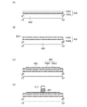
本実施の形態のストレージシステムの構成を図1に示す。図1(A)に示すストレージシステム100は、アレイコントローラ102、大容量の記憶デバイスであるハードディスク104(ハードディスク104a、ハードディスク104b、…)を有している。図1(A)に示すストレージシステム100において、アレイコントローラ102はホストコンピュータ(以下ホストという)101に電気的に接続されている。なお、本実施の形態のストレージシステムとして、RAID(Redundant Array Of Inexpensive Disks、又は、Redundant Array Of Independent Disks)システムを用いる。RAIDとは、複数のハードディスクを組み合わせて1台のハードディスクとして管理する技術である。
<Storage system configuration>
The configuration of the storage system of this embodiment is shown in FIG. A
ホスト101は、プロセッサ121、メモリ122、インターフェース123を有している。ホスト101のプロセッサ121は、他の装置の制御やデータの演算を行う装置である。ホスト101のプロセッサ121は、メモリ122に記憶されたプログラムを実行する装置である。ホスト101のプロセッサ121は、当該他の装置からインターフェース123を介してデータを受け取り、当該データを演算する。当該演算されたデータは、インターフェース123を介して当該他の装置に出力される。なお、ホスト101は複数設けてもよい。 The host 101 has a processor 121, a memory 122, and an interface 123. The processor 121 of the host 101 is a device that controls other devices and calculates data. The processor 121 of the host 101 is a device that executes a program stored in the memory 122. The processor 121 of the host 101 receives data from the other device via the interface 123 and calculates the data. The calculated data is output to the other device via the interface 123. A plurality of hosts 101 may be provided.
メモリ122は、プロセッサ121が実行するプログラムを記憶する機能や、プロセッサ121が演算を行う間データを格納する機能を有する。メモリ122として、上述の酸化物半導体トランジスタを用いた記憶装置(詳細は後述)、又は、酸化物半導体トランジスタを用いたメモリ及びDRAMを組み合わせた記憶装置を用いることができる。 The memory 122 has a function of storing a program executed by the processor 121 and a function of storing data while the processor 121 performs an operation. As the memory 122, a memory device using the above-described oxide semiconductor transistor (details will be described later), or a memory device in which a memory using an oxide semiconductor transistor and a DRAM are combined can be used.
当該演算されたデータは、ホスト101からアレイコントローラ102を介して、ハードディスク104に入力される。このとき、当該演算されたデータは、まずアレイコントローラ102のキャッシュメモリ103に記憶される。
The calculated data is input from the host 101 to the
アレイコントローラ102は、プロセッサ131、メモリ132、キャッシュメモリ103を有している。アレイコントローラ102は、複数の記憶デバイス(本実施の形態ではハードディスク104)を論理的に1つにまとめて制御し、ホスト101から入力されたデータが当該複数の記憶デバイスへどのように出力されるかを制御する。アレイコントローラ102として、例えばRAIDコントローラを用いることができる。なおアレイコントローラ102は複数設けてもよい。 The array controller 102 includes a processor 131, a memory 132, and a cache memory 103. The array controller 102 controls a plurality of storage devices (in this embodiment, the hard disk 104) in a logical manner and how the data input from the host 101 is output to the plurality of storage devices. To control. For example, a RAID controller can be used as the array controller 102. A plurality of array controllers 102 may be provided.
アレイコントローラ102のプロセッサ131は、メモリ132に記憶されたプログラムに基づいて、ホスト101から入力されたデータを、複数のハードディスク104(ハードディスク104a、ハードディスク104b、…)のうち、いずれかのハードディスクに記憶させるのかを指定する機能を有する。なお当該データが記憶されるハードディスクは、1つのハードディスクであってもよいし、複数のハードディスクであってもよい。
Based on a program stored in the memory 132, the processor 131 of the array controller 102 stores data input from the host 101 in any of the plurality of hard disks 104 (
メモリ132は、プロセッサ131が実行するプログラムを記憶する機能や、プロセッサ131が処理(例えば、上述のデータが記憶されるハードディスクの指定)を行う間にデータを格納する機能を有する。メモリ132として、メモリ122と同様に、上述の酸化物半導体トランジスタを用いた記憶装置(構成の詳細は後述)、又は、酸化物半導体トランジスタを用いたメモリ及びDRAMを組み合わせた記憶装置を用いる。 The memory 132 has a function of storing a program executed by the processor 131 and a function of storing data while the processor 131 performs processing (for example, designation of a hard disk storing the above-described data). As the memory 132, similarly to the memory 122, a memory device using the above-described oxide semiconductor transistor (details of the configuration will be described later) or a memory device in which a memory using an oxide semiconductor transistor and a DRAM are combined is used.
アレイコントローラ102のキャッシュメモリ103に記憶されたデータは、プロセッサ131によって指定された、複数のハードディスク104のうちいずれかに記憶される。上述のように、当該データが記憶されるハードディスクは、1つのハードディスクであってもよいし、複数のハードディスクであってもよい。これにより、ホスト101から入力されたデータが、ハードディスク104へどのように出力されるか(どのハードディスクに出力されるか、1つのハードディスクなのか複数なのか等)が制御される。
Data stored in the cache memory 103 of the array controller 102 is stored in one of the plurality of
なお、図1(A)では、アレイコントローラ102の内部にキャッシュメモリ103を設けたが、図1(B)のようにアレイコントローラ102の外部にキャッシュメモリ103を設けてもよい。 In FIG. 1A, the cache memory 103 is provided inside the array controller 102, but the cache memory 103 may be provided outside the array controller 102 as shown in FIG.
キャッシュメモリ103は、酸化物半導体トランジスタを用いた記憶装置である。上述のように、酸化物半導体トランジスタは、オフ電流が極めて小さいため、酸化物半導体トランジスタのソースまたはドレインの一方と電気的に接続されたノードの電荷(データ)を長時間にわたって保持することが可能となる。このようなオフ電流がきわめて小さい酸化物半導体トランジスタを用いた記憶装置は、電力の供給がなくなっても記憶内容が失われない。そのため、停電時の電源確保のためキャッシュメモリ用の蓄電装置は不要である。 The cache memory 103 is a storage device using an oxide semiconductor transistor. As described above, an off-state current of an oxide semiconductor transistor is extremely small, so that charge (data) of a node electrically connected to one of a source and a drain of the oxide semiconductor transistor can be held for a long time. It becomes. In such a memory device using an oxide semiconductor transistor with extremely small off-state current, stored data is not lost even when power is not supplied. For this reason, a power storage device for a cache memory is not required for securing a power supply during a power failure.
また、酸化物半導体トランジスタは、オフ電流が極めて小さいため、リフレッシュ動作が不要、又は、リフレッシュ動作の頻度を極めて低くすることが可能となるため、キャッシュメモリ103、さらにはストレージシステムの消費電力を十分に低減することができる。 In addition, since the off-state current of the oxide semiconductor transistor is extremely small, the refresh operation is not necessary or the frequency of the refresh operation can be extremely low. Therefore, the power consumption of the cache memory 103 and the storage system can be sufficiently increased. Can be reduced.
また酸化物半導体トランジスタを用いた記憶装置は、フラッシュメモリのように記憶素子のゲート絶縁層が劣化することがないので、書き込み回数に上限値がない。よって、酸化物半導体トランジスタを用いた記憶装置をキャッシュメモリ103として用いると、書き込み回数に制限がないストレージシステムを提供することができる。 In addition, in a memory device using an oxide semiconductor transistor, the gate insulating layer of the memory element does not deteriorate unlike a flash memory, and thus there is no upper limit on the number of times of writing. Therefore, when a memory device including an oxide semiconductor transistor is used as the cache memory 103, a storage system in which the number of writing operations is not limited can be provided.
なお、酸化物半導体トランジスタ及びそれを用いた記憶装置の構成の詳細な説明は後述する。 Note that a detailed description of the structure of the oxide semiconductor transistor and the memory device using the oxide semiconductor transistor will be described later.
<ストレージシステムの動作>
図2に本実施の形態のストレージシステムの動作を示す。ホスト101からストレージシステム100へのデータの書き込み処理が開始されると(ステップS101)、キャッシュメモリ103に空き領域があるか確認が行われる。キャッシュメモリ103に空き領域が確保された場合(ステップS102)、キャッシュメモリ103の当該空き領域にデータが入力される(ステップS103)。
<Storage system operation>
FIG. 2 shows the operation of the storage system of this embodiment. When data write processing from the host 101 to the
キャッシュメモリ103に空き領域がなかった場合(ステップS102)、キャッシュメモリ103のうち参照回数が最も小さいデータを検索する(ステップS111)。参照回数とは、そのデータが参照された(読み出された、又は、使用された)回数であり、参照回数が小さいということは、必要度の低いデータということである。 If there is no free space in the cache memory 103 (step S102), the cache memory 103 is searched for data with the smallest reference count (step S111). The reference count is the number of times the data has been referenced (read or used), and a low reference count means data with a low necessity.
キャッシュメモリ103に空き領域がなかった場合は、新たに書き込まれるデータを、当該参照回数が最も小さいデータが記憶されている領域に入力される(ステップS103)。なお、キャッシュメモリ103に空き領域がなかった場合に新たなデータを書き込む領域は、あらかじめ決められた方法によって選択されたその他の領域でもよい。 If there is no free area in the cache memory 103, the newly written data is input to the area where the data with the smallest reference count is stored (step S103). It should be noted that the area where new data is written when there is no free area in the cache memory 103 may be another area selected by a predetermined method.
キャッシュメモリ103へのデータの入力終了後、ホスト101へ入力処理終了の情報を送信する(ステップS104)。 After the input of data to the cache memory 103 is completed, information on the completion of input processing is transmitted to the host 101 (step S104).
ホスト101への入力処理終了の情報を送信後、キャッシュメモリ103に記憶されたデータが、ハードディスク104に出力される(ステップS105)。この際、キャッシュメモリ103に記憶されているデータには、ハードディスク104に出力されたことを識別できるフラグが立てられる。なお、次のデータがキャッシュメモリ103に入力される際には、すでにキャッシュメモリ103にあるデータとそのフラグは上書きされる。
After transmitting the input processing end information to the host 101, the data stored in the cache memory 103 is output to the hard disk 104 (step S105). At this time, a flag that can identify that the data has been output to the
以上で、データの書き込み処理を終了する(ステップS106)。 This completes the data writing process (step S106).
ただし、ステップS101乃至ステップS106の動作は、予期しない停電や予期しないシステム停止が起こらなかった場合の動作である。ホスト101からキャッシュメモリ103にデータが入力された後、ホスト101へ入力処理終了の情報を送信する(ステップS104)際、又は、キャッシュメモリ103に記憶されたデータが、ハードディスク104に出力される(ステップS105)際に、予期しない停電や予期しないシステム停止が起こった場合、以下に示す動作に移行する。 However, the operations in steps S101 to S106 are operations when an unexpected power failure or unexpected system stop does not occur. After data is input from the host 101 to the cache memory 103, information indicating completion of input processing is transmitted to the host 101 (step S104), or data stored in the cache memory 103 is output to the hard disk 104 ( If an unexpected power failure or unexpected system stop occurs at step S105), the operation proceeds to the following operation.
予期しない停電や予期しないシステム停止が起こった場合、直後にストレージシステム100は動作を停止する。ただし、キャッシュメモリ103は、酸化物半導体を用いた記憶装置を有するので、外部から電源が供給されなくても一定時間(例えば、10時間以上)データを保持できる。予期しない停電や予期しないシステム停止が復旧すると、まず、ストレージシステム100のキャッシュメモリ103以外の部分(例えば、ハードディスク104等)を再起動する(部分再起動、ステップS120)。なお、この際、ホスト101その他も再起動してもよい。また、キャッシュメモリ103も、データを失わないのであれば、再起動してもよい。あるいは、ストレージシステム100は電源が復旧したら、自動的にハードディスクにアクセスできるような構造(自動再起動する構造)で構成されてもよい。いずれにせよ、キャッシュメモリ103に保持されているデータは失われることがなく、そして、ハードディスクに入力できる状態とすることが求められる。
When an unexpected power failure or an unexpected system stop occurs, the
次に、キャッシュメモリ103に未出力のデータが存在するかどうかをホスト101またはストレージシステム100が確認する(ステップS121)。この過程は、復帰後、自動的におこなわれるようにプログラムされていてもよい。キャッシュメモリ103にデータが存在する場合(ステップS121)、当該データがハードディスク104に出力される(ステップS122)。その後、動作を終了する(ステップS123)。
Next, the host 101 or the
キャッシュメモリ103にデータが存在しない場合はそのまま、動作を終了する(ステップS123)。 If there is no data in the cache memory 103, the operation is terminated as it is (step S123).
以上で、予期しない停電や予期しないシステム停止が起こった場合のストレージシステムへの書き込み動作を終了する。必要に応じては、ステップS122とS123の間に、ストレージシステム100およびホスト101の再起動を手動もしくは自動で行うように設定されていてもよい。再起動後は、インターフェース123に外部からデータが入力されると、再度ステップS101からの過程によって、データをハードディスク104に入力する。以上の操作は、ホスト101あるいはストレージシステム100のいずれかに設けられた読み出し可能な記憶装置中にコンピュータプログラムとして格納され、ホスト101あるいはストレージシステム100のいずれかにあるプロセッサにより実行される。なお、このプログラムはその他の記憶媒体中に保存されていてもよく、また、通信回線を通して、送信あるいは受信されることもある。また、第三者の要求に応じて、送信されることもある。さらには、何らかの中継地点(インターネットサーバ等)で中継されることもある。
This completes the write operation to the storage system in the event of an unexpected power failure or unexpected system stop. If necessary, the
<酸化物半導体トランジスタを用いた記憶装置の構成>
図1に示すキャッシュメモリ103の構成について以下に説明する。図1に示すキャッシュメモリ103は、酸化物半導体トランジスタを用いた記憶装置である。さらには、ホスト101に含まれるメモリ122、及びアレイコントローラ102に含まれるメモリ132についても、酸化物半導体トランジスタを用いた記憶装置を用いてもよい。
<Structure of Memory Device Using Oxide Semiconductor Transistor>
The configuration of the cache memory 103 shown in FIG. 1 will be described below. A cache memory 103 illustrated in FIG. 1 is a memory device using an oxide semiconductor transistor. Further, a memory device using an oxide semiconductor transistor may be used for the memory 122 included in the host 101 and the memory 132 included in the array controller 102.
<<酸化物半導体トランジスタの構成>>
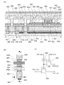
まず、図3に、本実施の形態の酸化物半導体トランジスタの構成を示す。図3(A)乃至図3(C)に示すトランジスタ440aは、トップゲート構造であり、酸化物半導体層を活性層として有する酸化物半導体トランジスタの一例である。図3(A)は平面図であり、図3(A)中の一点鎖線X1−X2で切断した断面が図3(B)に相当し、図3(A)中の一点鎖線Y1−Y2で切断した断面が図3(C)に相当する。
<< Configuration of Oxide Semiconductor Transistor >>
First, FIG. 3 illustrates a structure of the oxide semiconductor transistor of this embodiment. A
チャネル長方向の断面図である図3(B)及びチャネル幅方向の断面図である図3(C)に示すように、トランジスタ440aを含む半導体装置は、下地絶縁層436が設けられた絶縁表面を有する基板400上に、酸化物半導体層403、ソース電極層405a、ドレイン電極層405b、ゲート絶縁層402、ゲート電極層401、ゲート電極層401の側面に設けられた側壁絶縁層412、ゲート電極層401上に設けられた絶縁層413、ソース電極層405a及びドレイン電極層405b上に設けられた層間絶縁層417、層間絶縁層417上に設けられた層間絶縁層415、トランジスタ440aを覆う絶縁層407を有する。なお、図面をわかりやすくするため、図3(A)では一部の構成要素の記載を省略している。
As shown in FIG. 3B, which is a cross-sectional view in the channel length direction, and FIG. 3C, which is a cross-sectional view in the channel width direction, the semiconductor device including the
また、本実施の形態に示す下地絶縁層436は、第1の下地絶縁層436a及び第2の下地絶縁層436bの積層により構成する例を示している。また、本実施の形態に示すゲート絶縁層402は、第1のゲート絶縁層402a及び第2のゲート絶縁層402bの積層により構成する例を示している。第1の下地絶縁層436a、第2のゲート絶縁層402b、層間絶縁層417は、水素、水分、水素化物、または水酸化物などの不純物や、酸素に対するバリア性を有する材料を用いることが好ましい。上記絶縁層にバリア性を有する材料を適用することで、外部からの不純物の浸入を防ぐとともに、酸化物半導体層403、第2の下地絶縁層436b、第1のゲート絶縁層402aからの酸素の脱離を防ぐことができる。
In addition, the
層間絶縁層415はトランジスタ440aによる凹凸を平坦化するように設けられており、該上面の高さ(基板400表面からの垂直距離)は側壁絶縁層412、及び絶縁層413と概略同じである。また、ソース電極層405a及びドレイン電極層405bの上面の高さは、層間絶縁層415、側壁絶縁層412、及び絶縁層413の上面の高さより低く、ゲート電極層401の上面の高さより高い。
The interlayer insulating
また、図3において、絶縁層407は、層間絶縁層415、層間絶縁層417、ソース電極層405a、ドレイン電極層405b、側壁絶縁層412、絶縁層413と接して設けられている。
In FIG. 3, the insulating
なお、本明細書中において、酸化物半導体層403中のゲート電極層401と重畳する領域を、チャネル形成領域と言い、酸化物半導体層403中のソース電極層405aと接する領域をソース領域と言い、酸化物半導体層403中のドレイン電極層405bと接する領域をドレイン領域と言う。また、酸化物半導体層403中のチャネル形成領域とソース領域の間の領域をオフセット領域406aと言い、チャネル形成領域とドレイン領域の間の領域をオフセット領域406bと言う。オフセット領域406a、及びオフセット領域406bは、酸化物半導体層403中の側壁絶縁層412と重畳する位置に形成される。
Note that in this specification, a region overlapping with the
すなわち、チャネル形成領域、ソース領域、ドレイン領域、オフセット領域406a、オフセット領域406bは、自己整合により形成される。なお、オフセット領域を設けることによりゲート電極層401とソース電極層405a間に生じる寄生容量を低減することができる。また、ゲート電極層401とドレイン電極層405b間に生じる寄生容量を低減することができる。
That is, the channel formation region, the source region, the drain region, the offset
また、自己整合によりチャネル形成領域が形成されるため、トランジスタの微細化が実現し易く、オン特性(例えば、オン電流及び電界効果移動度)が高く、高速動作が可能となる。 In addition, since a channel formation region is formed by self-alignment, miniaturization of a transistor is easily realized, on-state characteristics (eg, on-current and field-effect mobility) are high, and high-speed operation is possible.
一方、後述する作製工程において、酸化物半導体層403に、ゲート電極層401をマスクとして、酸化物半導体の導電性を変化させる不純物元素が添加される場合は、ソース領域及びチャネル形成領域との間、並びに、ドレイン領域及びチャネル形成領域との間に、自己整合的に低抵抗領域が形成される。当該低抵抗領域が形成されると、トランジスタ440aのオン抵抗を低減し、動作速度を向上させることができる。
On the other hand, in the manufacturing process described later, in the case where an impurity element that changes conductivity of the oxide semiconductor is added to the
酸化物半導体層403に用いる酸化物半導体としては、少なくともインジウム(In)または亜鉛(Zn)を含むことが好ましい。特にInとZnを含むことが好ましい。また、該酸化物半導体を用いたトランジスタの電気特性のばらつきを減らすためのスタビライザーとして、それらに加えてガリウム(Ga)を有することが好ましい。また、スタビライザーとしてスズ(Sn)を有することが好ましい。また、スタビライザーとしてハフニウム(Hf)を有することが好ましい。また、スタビライザーとしてアルミニウム(Al)を有することが好ましい。また、スタビライザーとしてジルコニウム(Zr)を有することが好ましい。
An oxide semiconductor used for the
また、他のスタビライザーとして、ランタノイドである、ランタン(La)、セリウム(Ce)、プラセオジム(Pr)、ネオジム(Nd)、サマリウム(Sm)、ユウロピウム(Eu)、ガドリニウム(Gd)、テルビウム(Tb)、ジスプロシウム(Dy)、ホルミウム(Ho)、エルビウム(Er)、ツリウム(Tm)、イッテルビウム(Yb)、ルテチウム(Lu)のいずれか一種あるいは複数種を有してもよい。 As other stabilizers, lanthanoids such as lanthanum (La), cerium (Ce), praseodymium (Pr), neodymium (Nd), samarium (Sm), europium (Eu), gadolinium (Gd), terbium (Tb) , Dysprosium (Dy), holmium (Ho), erbium (Er), thulium (Tm), ytterbium (Yb), or lutetium (Lu).
例えば、酸化物半導体層403として、酸化インジウム、酸化スズ、酸化亜鉛、In−Zn系酸化物、Sn−Zn系酸化物、Al−Zn系酸化物、Zn−Mg系酸化物、Sn−Mg系酸化物、In−Mg系酸化物、In−Ga系酸化物、In−Ga−Zn系酸化物(IGZOとも表記する)、In−Al−Zn系酸化物、In−Sn−Zn系酸化物、Sn−Ga−Zn系酸化物、Al−Ga−Zn系酸化物、Sn−Al−Zn系酸化物、In−Hf−Zn系酸化物、In−La−Zn系酸化物、In−Ce−Zn系酸化物、In−Pr−Zn系酸化物、In−Nd−Zn系酸化物、In−Sm−Zn系酸化物、In−Eu−Zn系酸化物、In−Gd−Zn系酸化物、In−Tb−Zn系酸化物、In−Dy−Zn系酸化物、In−Ho−Zn系酸化物、In−Er−Zn系酸化物、In−Tm−Zn系酸化物、In−Yb−Zn系酸化物、In−Lu−Zn系酸化物、In−Sn−Ga−Zn系酸化物、In−Hf−Ga−Zn系酸化物、In−Al−Ga−Zn系酸化物、In−Sn−Al−Zn系酸化物、In−Sn−Hf−Zn系酸化物、In−Hf−Al−Zn系酸化物を用いることができる。
For example, the
なお、ここで、例えば、In−Ga−Zn系酸化物とは、InとGaとZnを主成分として有する酸化物という意味であり、InとGaとZnの比率は問わない。また、InとGaとZn以外の金属元素が入っていてもよい。 Note that here, for example, an In—Ga—Zn-based oxide means an oxide containing In, Ga, and Zn as its main components, and there is no limitation on the ratio of In, Ga, and Zn. Moreover, metal elements other than In, Ga, and Zn may be contained.
また、酸化物半導体として、InMO3(ZnO)m(m>0)で表記される材料を用いてもよい。なお、Mは、Ga、Fe、Mn及びCoから選ばれた一の金属元素または複数の金属元素を示す。また、酸化物半導体として、In2SnO5(ZnO)n(n>0)で表記される材料を用いてもよい。 Alternatively, a material represented by InMO 3 (ZnO) m (m> 0) may be used as the oxide semiconductor. Note that M represents one metal element or a plurality of metal elements selected from Ga, Fe, Mn, and Co. Alternatively, a material represented by In 2 SnO 5 (ZnO) n (n> 0) may be used as the oxide semiconductor.
例えば、In:Ga:Zn=1:1:1(=1/3:1/3:1/3)、In:Ga:Zn=2:2:1(=2/5:2/5:1/5)、あるいはIn:Ga:Zn=3:1:2(=1/2:1/6:1/3)の原子数比のIn−Ga−Zn系酸化物やその組成の近傍の酸化物を用いることができる。あるいは、In:Sn:Zn=1:1:1(=1/3:1/3:1/3)、In:Sn:Zn=2:1:3(=1/3:1/6:1/2)あるいはIn:Sn:Zn=2:1:5(=1/4:1/8:5/8)の原子数比のIn−Sn−Zn系酸化物やその組成の近傍の酸化物を用いるとよい。 For example, In: Ga: Zn = 1: 1: 1 (= 1/3: 1/3: 1/3), In: Ga: Zn = 2: 2: 1 (= 2/5: 2/5: 1) / 5), or an In—Ga—Zn-based oxide having an atomic ratio of In: Ga: Zn = 3: 1: 2 (= 1/2: 1/6: 1/3) and oxidation in the vicinity of the composition. Can be used. Alternatively, In: Sn: Zn = 1: 1: 1 (= 1/3: 1/3: 1/3), In: Sn: Zn = 2: 1: 3 (= 1/3: 1/6: 1) / 2) or In: Sn: Zn = 2: 1: 5 (= 1/4: 1/8: 5/8) atomic ratio In—Sn—Zn-based oxide or oxide in the vicinity of the composition Should be used.
しかし、これらに限られず、必要とする半導体特性(移動度、しきい値、ばらつき等)に応じて適切な組成のものを用いればよい。また、必要とする半導体特性を得るために、キャリア濃度や不純物濃度、欠陥密度、金属元素と酸素の原子数比、原子間距離、密度等を適切なものとすることが好ましい。 However, the composition is not limited thereto, and a material having an appropriate composition may be used depending on required semiconductor characteristics (mobility, threshold value, variation, etc.). In order to obtain the required semiconductor characteristics, it is preferable that the carrier concentration, the impurity concentration, the defect density, the atomic ratio between the metal element and oxygen, the interatomic distance, the density, and the like are appropriate.
例えば、In−Sn−Zn系酸化物では比較的容易に高い移動度が得られる。しかしながら、In−Ga−Zn系酸化物でも、バルク内欠陥密度を低くすることにより移動度を上げることができる。 For example, high mobility can be obtained relatively easily with an In—Sn—Zn-based oxide. However, mobility can be increased by reducing the defect density in the bulk also in the case of using an In—Ga—Zn-based oxide.
なお、例えば、In、Ga、Znの原子数比がIn:Ga:Zn=a:b:c(a+b+c=1)である酸化物の組成が、原子数比がIn:Ga:Zn=A:B:C(A+B+C=1)の酸化物の組成の近傍であるとは、a、b、cが、(a−A)2+(b−B)2+(c−C)2≦r2を満たすことをいう。rとしては、例えば、0.05とすればよい。他の酸化物でも同様である。 Note that for example, the composition of an oxide in which the atomic ratio of In, Ga, and Zn is In: Ga: Zn = a: b: c (a + b + c = 1) has an atomic ratio of In: Ga: Zn = A: B: C (A + B + C = 1) is in the vicinity of the oxide composition, a, b, c are (a−A) 2 + (b−B) 2 + (c−C) 2 ≦ r 2 Satisfying. For example, r may be 0.05. The same applies to other oxides.
しかし、これらに限られず、必要とする半導体特性(電界効果移動度、しきい値電圧等)に応じて適切な組成のものを用いればよい。また、必要とする半導体特性を得るために、キャリア濃度や不純物濃度、欠陥密度、金属元素と酸素の原子数比、原子間距離、密度等を適切なものとすることが好ましい。 However, the composition is not limited to these, and a material having an appropriate composition may be used depending on required semiconductor characteristics (field effect mobility, threshold voltage, and the like). In order to obtain the required semiconductor characteristics, it is preferable that the carrier concentration, the impurity concentration, the defect density, the atomic ratio between the metal element and oxygen, the interatomic distance, the density, and the like are appropriate.
また、酸化物半導体を半導体層中のチャネル形成領域に用いたトランジスタは、酸化物半導体を高純度化することにより、オフ電流(上述のように、オフ状態のとき、例えばソース電位を基準としたときのゲート電位との電位差がしきい値電圧以下のときのドレイン電流)を十分に低くすることが可能である。例えば、加熱成膜により水素や水酸基を酸化物半導体中に含ませないようにし、または成膜後の加熱により膜中から除去し、高純度化を図ることができる。高純度化されることにより、チャネル形成領域にIn−Ga−Zn系酸化物を用いたトランジスタで、チャネル長が10μm、半導体膜の膜厚が30nm、ドレイン電圧が1V〜10V程度の範囲である場合、オフ電流を、1×10⁻¹³A以下とすることが可能である。またチャネル幅あたりのオフ電流(オフ電流をトランジスタのチャネル幅で除した値)を1×10⁻²³A/μm(10yA/μm)から1×10−22A/μm(100yA/μm)程度とすることが可能である。 In addition, a transistor in which an oxide semiconductor is used for a channel formation region in a semiconductor layer has a high-purity oxide semiconductor, so that an off-state current (for example, a source potential is used as a reference when the transistor is off as described above. The drain current when the potential difference with the gate potential is equal to or lower than the threshold voltage can be sufficiently reduced. For example, hydrogen or a hydroxyl group can be prevented from being included in the oxide semiconductor by heat film formation, or can be removed from the film by heat after film formation, so that high purity can be achieved. By being highly purified, a transistor using an In—Ga—Zn-based oxide in a channel formation region has a channel length of 10 μm, a semiconductor film thickness of 30 nm, and a drain voltage of about 1 V to 10 V. In this case, the off-current can be 1 × 10 −13 A or less. The off current per channel width (the value obtained by dividing the off current by the channel width of the transistor) is about 1 × 10 −23 A / μm (10 yA / μm) to 1 × 10 −22 A / μm (100 yA / μm). Is possible.
なお酸化物半導体を高純度化して極小となるオフ電流を検出するためには、比較的サイズの大きいトランジスタを作製し、オフ電流を測定することで、実際に流れるオフ電流を見積もることができる。図12にはサイズの大きいトランジスタとして、チャネル幅Wを1m(1000000μm)、チャネル長Lを3μmとした際に、温度を150℃、125℃、85℃、27℃と変化させた際のチャネル幅W1μmあたりのオフ電流をアレニウスプロットした図を示す。図12に示されるように、オフ電流は3×10⁻²⁶A/μmと極めて小さいことがわかる。なお、昇温してオフ電流を測定したのは、室温では電流が極めて小さいため、測定が困難だったためである。 Note that in order to detect an off-state current that is minimized by purifying an oxide semiconductor, an off-state current that actually flows can be estimated by manufacturing a relatively large transistor and measuring the off-state current. FIG. 12 shows a large transistor having a channel width when the channel width W is 1 m (1000000 μm) and the channel length L is 3 μm, and the temperature is changed to 150 ° C., 125 ° C., 85 ° C., and 27 ° C. The figure which made the Arrhenius plot the off-current per W1micrometer is shown. As shown in FIG. 12, it can be seen that the off-state current is as extremely small as 3 × 10 −26 A / μm. The reason why the off-state current was measured by raising the temperature was that measurement was difficult because the current was extremely small at room temperature.
本実施の形態に開示する酸化物半導体膜は、例えば、非単結晶を有してもよい。非単結晶は、例えば、CAAC(C Axis Aligned Crystal)、多結晶、微結晶、非晶質部を有する。非晶質部は、微結晶、CAACよりも欠陥準位密度が高い。また、微結晶は、CAACよりも欠陥準位密度が高い。なお、CAACを有する酸化物半導体を、CAAC−OS(C Axis Aligned Crystalline Oxide Semiconductor)と呼ぶ。 The oxide semiconductor film disclosed in this embodiment may include a non-single crystal, for example. The non-single crystal includes, for example, CAAC (C Axis Aligned Crystal), polycrystal, microcrystal, and amorphous part. The amorphous part has a higher density of defect states than microcrystals and CAAC. In addition, microcrystals have a higher density of defect states than CAAC. Note that an oxide semiconductor including CAAC is referred to as a CAAC-OS (C Axis Crystallized Oxide Semiconductor).
酸化物半導体膜は、例えばCAAC−OSを有してもよい。CAAC−OSは、例えば、c軸配向し、a軸または/およびb軸はマクロに揃っていない。 For example, the oxide semiconductor film may include a CAAC-OS. For example, the CAAC-OS is c-axis oriented, and the a-axis and / or the b-axis are not aligned macroscopically.
酸化物半導体膜は、例えば微結晶を有してもよい。なお、微結晶を有する酸化物半導体を、微結晶酸化物半導体と呼ぶ。微結晶酸化物半導体膜は、例えば、1nm以上10nm未満のサイズの微結晶(ナノ結晶ともいう。)を膜中に含む。 The oxide semiconductor film may include microcrystal, for example. Note that an oxide semiconductor including microcrystal is referred to as a microcrystalline oxide semiconductor. The microcrystalline oxide semiconductor film includes microcrystal (also referred to as nanocrystal) with a size greater than or equal to 1 nm and less than 10 nm, for example.
酸化物半導体膜は、例えば非晶質部を有してもよい。なお、非晶質部を有する酸化物半導体を、非晶質酸化物半導体と呼ぶ。非晶質酸化物半導体膜は、例えば、原子配列が無秩序であり、結晶成分を有さない。または、非晶質酸化物半導体膜は、例えば、完全な非晶質であり、結晶部を有さない。 For example, the oxide semiconductor film may include an amorphous part. Note that an oxide semiconductor having an amorphous part is referred to as an amorphous oxide semiconductor. An amorphous oxide semiconductor film has, for example, disordered atomic arrangement and no crystal component. Alternatively, the amorphous oxide semiconductor film is, for example, completely amorphous and has no crystal part.
なお、酸化物半導体膜が、CAAC−OS、微結晶酸化物半導体、非晶質酸化物半導体の混合膜であってもよい。混合膜は、例えば、非晶質酸化物半導体の領域と、微結晶酸化物半導体の領域と、CAAC−OSの領域と、を有する。また、混合膜は、例えば、非晶質酸化物半導体の領域と、微結晶酸化物半導体の領域と、CAAC−OSの領域と、の積層構造を有してもよい。 Note that the oxide semiconductor film may be a mixed film of a CAAC-OS, a microcrystalline oxide semiconductor, and an amorphous oxide semiconductor. For example, the mixed film includes an amorphous oxide semiconductor region, a microcrystalline oxide semiconductor region, and a CAAC-OS region. The mixed film may have a stacked structure of an amorphous oxide semiconductor region, a microcrystalline oxide semiconductor region, and a CAAC-OS region, for example.
なお、酸化物半導体膜は、例えば、単結晶を有してもよい。 Note that the oxide semiconductor film may include a single crystal, for example.
酸化物半導体膜は、複数の結晶部を有し、当該結晶部のc軸が被形成面の法線ベクトルまたは表面の法線ベクトルに平行な方向に揃っていることが好ましい。なお、異なる結晶部間で、それぞれa軸およびb軸の向きが異なっていてもよい。そのような酸化物半導体膜の一例としては、CAAC−OS膜がある。 The oxide semiconductor film preferably includes a plurality of crystal parts, and the c-axis of the crystal parts is aligned in a direction parallel to the normal vector of the formation surface or the normal vector of the surface. Note that the directions of the a-axis and the b-axis may be different between different crystal parts. An example of such an oxide semiconductor film is a CAAC-OS film.
CAAC−OS膜に含まれる結晶部は、一辺が100nm未満の立方体内に収まる大きさであることが多い。また、透過型電子顕微鏡(TEM:Transmission Electron Microscope)による観察像では、CAAC−OS膜に含まれる結晶部と結晶部との境界は明確ではない。また、TEMによってCAAC−OS膜には明確な粒界(グレインバウンダリーともいう。)は確認できない。そのため、CAAC−OS膜は、粒界に起因する電子移動度の低下が抑制される。 In most cases, a crystal part included in the CAAC-OS film fits in a cube whose one side is less than 100 nm. Further, in the observation image obtained by a transmission electron microscope (TEM), the boundary between the crystal part and the crystal part included in the CAAC-OS film is not clear. In addition, a clear grain boundary (also referred to as a grain boundary) cannot be confirmed in the CAAC-OS film by TEM. Therefore, in the CAAC-OS film, reduction in electron mobility due to grain boundaries is suppressed.
CAAC−OS膜に含まれる結晶部は、例えば、c軸がCAAC−OS膜の被形成面の法線ベクトルまたは表面の法線ベクトルに平行な方向になるように揃い、かつab面に垂直な方向から見て金属原子が三角形状または六角形状に配列し、c軸に垂直な方向から見て金属原子が層状または金属原子と酸素原子とが層状に配列している。なお、異なる結晶部間で、それぞれa軸およびb軸の向きが異なっていてもよい。本明細書において、単に垂直と記載する場合、80°以上100°以下、好ましくは85°以上95°以下の範囲も含まれることとする。また、単に平行と記載する場合、−10°以上10°以下、好ましくは−5°以上5°以下の範囲も含まれることとする。 The crystal part included in the CAAC-OS film is aligned so that, for example, the c-axis is in a direction parallel to the normal vector of the formation surface of the CAAC-OS film or the normal vector of the surface, and is perpendicular to the ab plane. When viewed from the direction, the metal atoms are arranged in a triangular shape or a hexagonal shape, and when viewed from the direction perpendicular to the c-axis, the metal atoms are arranged in layers, or the metal atoms and oxygen atoms are arranged in layers. Note that the directions of the a-axis and the b-axis may be different between different crystal parts. In this specification, the term “perpendicular” includes a range of 80 ° to 100 °, preferably 85 ° to 95 °. In addition, a simple term “parallel” includes a range of −10 ° to 10 °, preferably −5 ° to 5 °.
なお、CAAC−OS膜において、結晶部の分布が一様でなくてもよい。例えば、CAAC−OS膜の形成過程において、酸化物半導体膜の表面側から結晶成長させる場合、被形成面の近傍に対し表面の近傍では結晶部の占める割合が高くなることがある。また、CAAC−OS膜へ不純物を添加することにより、当該不純物添加領域において結晶部の結晶性が低下することもある。 Note that the distribution of crystal parts in the CAAC-OS film is not necessarily uniform. For example, in the formation process of the CAAC-OS film, when crystal growth is performed from the surface side of the oxide semiconductor film, the ratio of crystal parts in the vicinity of the surface of the oxide semiconductor film is higher in the vicinity of the surface. Further, when an impurity is added to the CAAC-OS film, the crystallinity of a crystal part in the impurity-added region may be decreased.
CAAC−OS膜に含まれる結晶部のc軸は、CAAC−OS膜の被形成面の法線ベクトルまたは表面の法線ベクトルに平行な方向になるように揃うため、CAAC−OS膜の形状(被形成面の断面形状または表面の断面形状)によっては互いに異なる方向を向くことがある。また、結晶部は、成膜したとき、または成膜後に加熱処理などの結晶化処理を行ったときに形成される。従って、結晶部のc軸は、CAAC−OS膜が形成されたときの被形成面の法線ベクトルまたは表面の法線ベクトルに平行な方向になるように揃う。 Since the c-axis of the crystal part included in the CAAC-OS film is aligned in a direction parallel to the normal vector of the formation surface of the CAAC-OS film or the normal vector of the surface, the shape of the CAAC-OS film ( Depending on the cross-sectional shape of the surface to be formed or the cross-sectional shape of the surface, the directions may be different from each other. The crystal part is formed when a film is formed or when a crystallization process such as a heat treatment is performed after the film formation. Therefore, the c-axes of the crystal parts are aligned in a direction parallel to the normal vector of the surface where the CAAC-OS film is formed or the normal vector of the surface.
CAAC−OS膜を用いたトランジスタは、可視光や紫外光の照射による電気特性の変動が小さい。よって、当該トランジスタは、信頼性が高い。 In a transistor using a CAAC-OS film, change in electrical characteristics due to irradiation with visible light or ultraviolet light is small. Therefore, the transistor has high reliability.
なお、酸化物半導体層を構成する酸素の一部は窒素で置換されてもよい。 Note that part of oxygen included in the oxide semiconductor layer may be replaced with nitrogen.
また、CAAC−OSのように結晶部を有する酸化物半導体では、よりバルク内欠陥を低減することができ、表面の平坦性を高めれば非晶質状態の酸化物半導体以上の移動度を得ることができる。表面の平坦性を高めるためには、平坦な表面上に酸化物半導体を形成することが好ましく、具体的には、平均面粗さ(Ra)が1nm以下、好ましくは0.3nm以下、より好ましくは0.1nm以下の表面上に形成するとよい。 In addition, in an oxide semiconductor having a crystal part such as a CAAC-OS, defects in the bulk can be further reduced, and mobility higher than that of an oxide semiconductor in an amorphous state can be obtained by increasing surface flatness. Can do. In order to improve the flatness of the surface, it is preferable to form an oxide semiconductor on the flat surface. Specifically, the average surface roughness (Ra) is 1 nm or less, preferably 0.3 nm or less, more preferably Is preferably formed on a surface of 0.1 nm or less.
なお、Raは、JIS B0601で定義されている算術平均粗さを面に対して適用できるよう三次元に拡張したものであり、「基準面から指定面までの偏差の絶対値を平均した値」と表現できる。また、Raは原子間力顕微鏡(AFM:Atomic Force Microscope)にて測定可能である。 Note that Ra is an arithmetic mean roughness defined in JIS B0601 that has been expanded to three dimensions so that it can be applied to a surface. “A value obtained by averaging the absolute values of deviations from a reference surface to a specified surface” Can be expressed as Ra can be measured with an atomic force microscope (AFM).
酸化物半導体層の厚さは、1nm以上30nm以下(好ましくは5nm以上10nm以下)とし、スパッタリング法、MBE(Molecular Beam Epitaxy)法、CVD法、パルスレーザ堆積法、ALD(Atomic Layer Deposition)法等を適宜用いることができる。また、酸化物半導体層403は、スパッタリングターゲット表面に対し、概略垂直に複数の基板表面がセットされた状態で成膜を行うスパッタ装置を用いて成膜してもよい。
The thickness of the oxide semiconductor layer is 1 nm or more and 30 nm or less (preferably 5 nm or more and 10 nm or less). Can be used as appropriate. The
図4(A)乃至図4(D)及び図5(A)乃至図5(D)にトランジスタ440aを有する半導体装置の作製方法の一例を示す。
4A to 4D and FIGS. 5A to 5D illustrate an example of a method for manufacturing a semiconductor device including the
まず、基板400上に、第1の下地絶縁層436a及び第2の下地絶縁層436bを有する下地絶縁層436を形成する(図4(A)参照)。
First, the
基板400に使用することができる基板に大きな制限はないが、少なくとも、後の熱処理に耐えうる程度の耐熱性を有していることが必要となる。例えば、バリウムホウケイ酸ガラスやアルミノホウケイ酸ガラスなどのガラス基板、セラミック基板、石英基板、サファイア基板などを用いることができる。また、シリコンや炭化シリコンなどの単結晶半導体基板、多結晶半導体基板、シリコンゲルマニウムなどの化合物半導体基板、SOI基板などを適用することもでき、これらの基板上に半導体素子が設けられたものを、基板400として用いてもよい。
There is no particular limitation on a substrate that can be used as the
また、基板400として、可撓性基板を用いて半導体装置を作製してもよい。可撓性を有する半導体装置を作製するには、可撓性基板上に酸化物半導体層403を含むトランジスタ440aを直接作製してもよいし、他の作製基板に酸化物半導体層403を含むトランジスタ440aを作製し、その後可撓性基板に剥離、転置してもよい。なお、作製基板から可撓性基板に剥離、転置するために、作製基板と酸化物半導体層を含むトランジスタ440aとの間に剥離層を設けるとよい。
Alternatively, a semiconductor device may be manufactured using a flexible substrate as the
下地絶縁層436としては、プラズマCVD法又はスパッタリング法等により、酸化シリコン、窒化シリコン、酸化窒化シリコン、窒化酸化シリコン、酸化アルミニウム、窒化アルミニウム、酸化窒化アルミニウム、窒化酸化アルミニウム、酸化ハフニウム、酸化ガリウム、又はこれらの混合材料を用いて形成することができる。なお、本明細書において、酸化窒化物とは、その組成として、窒素よりも酸素の含有量が多いものを指し、窒化酸化物とは、その組成として、酸素よりも窒素の含有量が多いものを指すものとする。ここで、酸素及び窒素の含有量は、ラザフォード後方散乱法(RBS:Rutherford Backscattering Spectrometry)または水素前方散乱法(HFS:Hydrogen Forward scattering Spectrometry)を用いて測定するものとする。
As the
また、下地絶縁層436として、熱酸化膜を用いてもよい。熱酸化膜は、基板を酸化性雰囲気中で熱処理することで、基板表面を酸化させて形成することができる。例えば、基板400として単結晶シリコン基板を用いて、酸素を含む雰囲気や水蒸気を含む雰囲気中で、900℃乃至1200℃で数時間の熱処理を行うことで、基板400の表面に熱酸化膜を形成することができる。
Further, a thermal oxide film may be used as the
また、下地絶縁層436は、単層でも積層でもよいが、後述する酸化物半導体層403に近い方から順に、層中(バルク中)に少なくとも化学量論比を超える量の酸素が存在する絶縁層、及び、水素、水分、水素化物、または水酸化物などの不純物や、酸素に対するバリア性を有する絶縁層の積層であると、酸化物半導体層403に酸素を供給、かつ、酸化物半導体層403からの酸素の脱離を抑制することができるので好適である。本実施の形態では、下地絶縁層436として、第1の下地絶縁層436aと第2の下地絶縁層436bの積層を用いる。また、基板400上に形成する第1の下地絶縁層436aは、窒化シリコンや酸化アルミニウムなどの、水素、水分、水素化物、または水酸化物などの不純物や、酸素に対するバリア性を有する材料を用いることが好ましい。また、第1の下地絶縁層436a上に形成する第2の下地絶縁層436bは酸化物半導体層403と接するため、層中(バルク中)に少なくとも化学量論比を超える量の酸素が存在することが好ましい。例えば、第2の下地絶縁層436bとして、酸化シリコンを用いる場合には、SiO2+α(ただし、α>0)とする。このような第2の下地絶縁層436bを用いることで、酸化物半導体層403に酸素を供給することができ、特性を良好にすることができる。酸化物半導体層403へ酸素を供給することにより、酸化物半導体層403中の酸素欠損を補填することができる。
The
本実施の形態では、基板400として単結晶シリコン基板を用い、第1の下地絶縁層436aとして基板400上にプラズマCVD法により厚さ50nmの窒化シリコンを形成し、第1の下地絶縁層436a上に第2の下地絶縁層436bとして厚さ300nmの酸化シリコンを形成する。
In this embodiment, a single crystal silicon substrate is used as the
下地絶縁層436形成時の温度は、基板400が耐えうる温度以下で、より高いほうが好ましい。例えば、基板400を350℃以上450℃以下の温度に加熱しながら下地絶縁層436を形成する。なお、下地絶縁層436形成時の温度は一定であることが好ましい。例えば、下地絶縁層436の形成を、基板400を350℃に加熱して行う。
The temperature at which the
また、下地絶縁層436の形成後、減圧下、窒素雰囲気下、希ガス雰囲気下、または超乾燥エア窒素雰囲気下において、加熱処理を行ってもよい。加熱処理により下地絶縁層436に含まれる水素、水分、水素化物、または水酸化物などの濃度を低減することができる。加熱処理温度は、基板400が耐えうる温度以下で、より高い温度で行うことが好ましい。具体的には、下地絶縁層436の成膜温度以上、基板400の歪点以下で行うことが好ましい。
Further, after the
なお、下地絶縁層436の水素濃度は、5×10¹⁸atoms/cm3未満、好ましくは1×1018atoms/cm3以下、より好ましくは5×1017atoms/cm3以下、更に好ましくは1×1016atoms/cm3以下とすることが望ましい。
Note that the hydrogen concentration of the
第2の下地絶縁層436bの層中(バルク中)に少なくとも化学量論比を超える量の酸素が存在するためには、第2の下地絶縁層436bに酸素を供給してもよい。
Oxygen may be supplied to the second
酸素の供給により、第2の下地絶縁層436bを構成する元素と水素の間の結合、或いは該元素と水酸基の間の結合を切断するとともに、これらの水素または水酸基が酸素と反応することで水を生成するため、酸素の供給後に加熱処理を行うと、不純物である水素または水酸基が、水として脱離しやすくなる。このため、第2の下地絶縁層436bへ酸素を供給した後に加熱処理を行ってもよい。その後、さらに第2の下地絶縁層436bに酸素を供給し、第2の下地絶縁層436bを酸素過剰な状態としてもよい。また、第2の下地絶縁層436bへの酸素の供給と加熱処理は、それぞれを交互に複数回行ってもよい。また、加熱処理と酸素の供給を同時に行ってもよい。
By supplying oxygen, a bond between an element constituting the second
次に、下地絶縁層436上に酸化物半導体層403をスパッタリング法により形成する(図4(B)参照)。
Next, the
酸化物半導体層403の形成工程において、酸化物半導体層403に水素、又は水がなるべく含まれないようにするために、酸化物半導体層403の成膜の前処理として、スパッタリング装置の予備加熱室で下地絶縁層436が形成された基板を予備加熱し、基板及び下地絶縁層436に吸着した水素、水分などの不純物を脱離し排気することが好ましい。なお、予備加熱室に設ける排気手段はクライオポンプが好ましい。
In the formation process of the
下地絶縁層436において酸化物半導体層403が接して形成される領域に、平坦化処理を行ってもよい。平坦化処理としては、特に限定されないが、研磨処理(例えば、化学的機械研磨法)、ドライエッチング処理、プラズマ処理を用いることができる。
Planarization treatment may be performed on a region where the
プラズマ処理としては、例えば、アルゴンガスを導入してプラズマを発生させる逆スパッタリングを行うことができる。逆スパッタリングとは、アルゴン雰囲気下で基板側にRF電源を用いて電圧を印加して基板近傍にプラズマを形成して表面を改質する方法である。なお、アルゴン雰囲気に代えて窒素、ヘリウム、酸素などを用いてもよい。逆スパッタリングを行うと、下地絶縁層436の表面に付着している粉状物質(パーティクル、ごみともいう)を除去することができる。
As the plasma treatment, for example, reverse sputtering in which an argon gas is introduced to generate plasma can be performed. Inverse sputtering is a method in which a surface is modified by forming a plasma near the substrate by applying a voltage to the substrate side using an RF power source in an argon atmosphere. Note that nitrogen, helium, oxygen, or the like may be used instead of the argon atmosphere. When reverse sputtering is performed, powdery substances (also referred to as particles or dust) attached to the surface of the
平坦化処理として、研磨処理、ドライエッチング処理、プラズマ処理は複数回行ってもよく、それらを組み合わせて行ってもよい。また、組み合わせて行う場合、工程順も特に限定されず、下地絶縁層436表面の凹凸状態に合わせて適宜設定すればよい。
As the planarization treatment, the polishing treatment, the dry etching treatment, and the plasma treatment may be performed a plurality of times or in combination. In the case where the steps are performed in combination, the order of steps is not particularly limited, and may be set as appropriate depending on the uneven state of the surface of the
平坦化処理は、例えば、第2の下地絶縁層436bとして用いる酸化シリコン層表面に化学的機械研磨法により研磨処理(研磨条件:ポリウレタン系研磨布、シリカ系スラリー、スラリー温度室温、研磨圧0.001MPa、研磨時回転数(テーブル/スピンドル)60rpm/56rpm、研磨時間0.5分)を行い、酸化シリコン層表面における平均面粗さ(Ra)を約0.15nmとすればよい。
For example, the surface of the silicon oxide layer used as the second
なお、酸化物半導体層403を形成するためのスパッタリングガスは、希ガス(代表的にはアルゴン)雰囲気、酸素雰囲気、希ガス及び酸素の混合ガスを適宜用いる。また、スパッタリングガスには、水素、水、水酸基または水素化物などの不純物が除去された高純度ガスを用いることが好ましい。
Note that as a sputtering gas for forming the
なお、酸化物半導体層403は、酸素が多く含まれるような条件(例えば、酸素100%の雰囲気下でスパッタリング法により成膜を行うなど)で形成して、酸素を多く含むまたは酸素が過飽和な状態(好ましくは酸化物半導体が結晶状態における化学量論的組成に対し、酸素の含有量が過剰な領域が含まれている状態)とすることが好ましい。
Note that the
例えば、スパッタリング法を用いて酸化物半導体層を形成する場合、スパッタリングガスの酸素の占める割合が多い条件で行うことが好ましく、スパッタリングガスを酸素ガス100%として行うことが好ましい。スパッタリングガス中の酸素ガスの占める割合が多い条件、特に酸素ガス100%で成膜すると、例えば形成温度を300℃以上としても、酸化物半導体層中からのZnの放出が抑えられる。 For example, in the case where an oxide semiconductor layer is formed by a sputtering method, the sputtering gas is preferably used under a condition where the proportion of oxygen in the sputtering gas is large and the sputtering gas is preferably used as 100% oxygen gas. When a film is formed under a condition where the proportion of oxygen gas in the sputtering gas is large, particularly 100% oxygen gas, release of Zn from the oxide semiconductor layer can be suppressed even when the formation temperature is 300 ° C. or higher, for example.
酸化物半導体層403は、銅、アルミニウム、塩素などの不純物がほとんど含まれない高純度化されたものであることが望ましい。トランジスタの製造工程において、これらの不純物が混入または酸化物半導体層表面に付着する恐れのない工程を適宜選択することが好ましい。具体的には、酸化物半導体層403の銅濃度は1×10¹⁸atoms/cm3以下、好ましくは1×1017atoms/cm3以下とする。また、酸化物半導体層403のアルミニウム濃度は1×1018atoms/cm3以下とする。また、酸化物半導体層403の塩素濃度は2×1018atoms/cm3以下とする。
The
また、酸化物半導体層403中のナトリウム(Na)、リチウム(Li)、カリウム(K)などのアルカリ金属の濃度は、Naは5×1016cm−3以下、好ましくは1×1016cm−3以下、さらに好ましくは1×1015cm−3以下、Liは5×1015cm−3以下、好ましくは1×1015cm−3以下、Kは5×1015cm−3以下、好ましくは1×1015cm−3以下とすることが好ましい。
The concentration of alkali metal such as sodium (Na), lithium (Li), or potassium (K) in the
本実施の形態においては、酸化物半導体層403として、AC電源装置を有するスパッタリング装置を用いたスパッタリング法により、膜厚35nmのIn−Ga−Zn系酸化物(IGZO)を形成する。スパッタリング法で作製するためのターゲットとしては、組成として、In:Ga:Zn=3:1:2[原子数比]の金属酸化物ターゲットを用いる。
In this embodiment, as the
また、金属酸化物ターゲットの相対密度(充填率)は90%以上100%以下、好ましくは95%以上99.9%以下である。相対密度の高い金属酸化物ターゲットを用いることにより、成膜した酸化物半導体層403は緻密な膜とすることができる。
The relative density (filling rate) of the metal oxide target is 90% to 100%, preferably 95% to 99.9%. By using a metal oxide target with a high relative density, the formed
酸化物半導体層403を、成膜する際に用いるスパッタリングガスは水素、水、水酸基又は水素化物などの不純物が除去された高純度ガスを用いることが好ましい。
As a sputtering gas used for forming the
まず、減圧状態に保持された成膜室内に基板を保持する。そして、成膜室内の残留水分を除去しつつ水素及び水分が除去されたスパッタガスを導入し、上記ターゲットを用いて基板400上に酸化物半導体層403を成膜する。成膜室内の残留水分を除去するためには、吸着型の真空ポンプ、例えば、クライオポンプ、イオンポンプ、チタンサブリメーションポンプを用いることが好ましい。また、排気手段としては、ターボ分子ポンプにコールドトラップを加えたものであってもよい。クライオポンプを用いて排気した成膜室は、例えば、水素原子、水(H2O)など水素原子を含む化合物(より好ましくは炭素原子を含む化合物も)等が排気されるため、当該成膜室で成膜した酸化物半導体層403に含まれる不純物の濃度を低減できる。
First, a substrate is held in a film formation chamber held in a reduced pressure state. Then, a sputtering gas from which hydrogen and moisture are removed is introduced while moisture remaining in the deposition chamber is removed, and the
また、下地絶縁層436と酸化物半導体層403を大気に解放せずに連続的に形成してもよい。下地絶縁層436と酸化物半導体層403とを大気に曝露せずに連続して形成すると、下地絶縁層436表面に水素や水分などの不純物が付着することを防止することができる。
Alternatively, the
また、酸化物半導体層403形成後に、酸化物半導体層403中の過剰な水素(水や水酸基を含む)を除去(脱水化または脱水素化)するための加熱処理を行ってもよい。加熱処理の温度は、300℃以上700℃以下、または基板の歪み点未満とする。加熱処理は減圧下又は窒素雰囲気下などで行うことができる。例えば、加熱処理装置の一つである電気炉に基板を導入し、酸化物半導体層403に対して窒素雰囲気下450℃において1時間の加熱処理を行う。
Further, after the
なお、加熱処理装置は電気炉に限られず、抵抗発熱体などの発熱体からの熱伝導または熱輻射によって、被処理物を加熱する装置を用いてもよい。例えば、GRTA(Gas Rapid Thermal Anneal)装置、LRTA(Lamp Rapid Thermal Anneal)装置等のRTA(Rapid Thermal Anneal)装置を用いることができる。LRTA装置は、ハロゲンランプ、メタルハライドランプ、キセノンアークランプ、カーボンアークランプ、高圧ナトリウムランプ、高圧水銀ランプなどのランプから発する光(電磁波)の輻射により、被処理物を加熱する装置である。GRTA装置は、高温のガスを用いて加熱処理を行う装置である。高温のガスには、アルゴンなどの希ガス、または窒素のような、加熱処理によって被処理物と反応しない不活性ガスが用いられる。 Note that the heat treatment apparatus is not limited to an electric furnace, and an apparatus for heating an object to be processed by heat conduction or heat radiation from a heating element such as a resistance heating element may be used. For example, a rapid thermal annealing (RTA) device such as a GRTA (Gas Rapid Thermal Anneal) device or an LRTA (Lamp Rapid Thermal Anneal) device can be used. The LRTA apparatus is an apparatus that heats an object to be processed by radiation of light (electromagnetic waves) emitted from a lamp such as a halogen lamp, a metal halide lamp, a xenon arc lamp, a carbon arc lamp, a high pressure sodium lamp, or a high pressure mercury lamp. The GRTA apparatus is an apparatus that performs heat treatment using a high-temperature gas. As the high-temperature gas, an inert gas that does not react with an object to be processed by heat treatment, such as nitrogen or a rare gas such as argon, is used.
例えば、加熱処理として、650℃〜700℃の高温に加熱した不活性ガス中に基板を入れ、数分間加熱した後、基板を不活性ガス中から出すGRTAを行ってもよい。 For example, as the heat treatment, GRTA may be performed in which the substrate is placed in an inert gas heated to a high temperature of 650 ° C. to 700 ° C., heated for several minutes, and then the substrate is taken out of the inert gas.
なお、加熱処理においては、窒素、またはヘリウム、ネオン、アルゴン等の希ガスに、水、水素などが含まれないことが好ましい。または、熱処理装置に導入する窒素、またはヘリウム、ネオン、アルゴン等の希ガスの純度を、6N(99.9999%)以上好ましくは7N(99.99999%)以上(即ち不純物濃度を1ppm以下、好ましくは0.1ppm以下)とすることが好ましい。 Note that in the heat treatment, it is preferable that water, hydrogen, or the like be not contained in nitrogen or a rare gas such as helium, neon, or argon. Alternatively, the purity of nitrogen or a rare gas such as helium, neon, or argon introduced into the heat treatment apparatus is 6N (99.9999%) or more, preferably 7N (99.99999%) or more (that is, the impurity concentration is 1 ppm or less, preferably Is preferably 0.1 ppm or less).
また、加熱処理により酸化物半導体層403を加熱した後、同じ炉に高純度の酸素ガス、高純度の一酸化二窒素ガス、又は超乾燥エア(CRDS(キャビティリングダウンレーザー分光法)方式の露点計を用いて測定した場合の水分量が20ppm(露点換算で−55℃)以下、好ましくは1ppm以下、より好ましくは10ppb以下の空気)を導入してもよい。酸素ガスまたは一酸化二窒素ガスに、水、水素などが含まれないことが好ましい。または、熱処理装置に導入する酸素ガスまたは一酸化二窒素ガスの純度を、6N以上好ましくは7N以上(即ち、酸素ガスまたは一酸化二窒素ガス中の不純物濃度を1ppm以下、好ましくは0.1ppm以下)とすることが好ましい。酸素ガス又は一酸化二窒素ガスの作用により、脱水化または脱水素化処理による不純物の排除工程によって同時に減少してしまった酸化物半導体を構成する主成分材料である酸素を供給することによって、酸化物半導体内の酸素欠損が低減され、酸化物半導体層403をi型(真性)または実質的にi型化することができる。この点、シリコンなどのように不純物元素を添加してのi型化ではないため、酸化物半導体のi型化は従来にない技術思想を含むものといえる。
In addition, after heating the
脱水化又は脱水素化のための加熱処理は、酸化物半導体層の形成後であれば、島状の酸化物半導体層403の形成前に行ってもよく、形成後に行ってもよい。また、脱水化又は脱水素化のための加熱処理は、複数回行ってもよく、他の加熱処理と兼ねてもよい。
The heat treatment for dehydration or dehydrogenation may be performed before or after the formation of the island-shaped
また、脱水化又は脱水素化処理によって、酸化物半導体を構成する主成分材料である酸素が同時に脱離して減少してしまう恐れがある。酸化物半導体層において、酸素が脱離した箇所では酸素欠損が存在し、該酸素欠損に起因してトランジスタの電気的特性変動を招くドナー準位が生じてしまう。 Further, oxygen that is a main component material of the oxide semiconductor may be desorbed and reduced at the same time by dehydration or dehydrogenation treatment. In the oxide semiconductor layer, oxygen vacancies exist at locations where oxygen is released, and donor levels that cause fluctuations in electrical characteristics of the transistor are generated due to the oxygen vacancies.
このため、脱水化又は脱水素化処理を行った酸化物半導体層403に、酸素(少なくとも、酸素ラジカル、酸素原子、酸素イオン、のいずれかを含む)を供給してもよい。
Therefore, oxygen (including at least one of oxygen radicals, oxygen atoms, and oxygen ions) may be supplied to the
脱水化又は脱水素化処理を行った酸化物半導体層403に、酸素を供給することによって、脱水化または脱水素化処理による不純物の排除工程によって生じた酸化物半導体内の酸素欠損を低減し、酸化物半導体層403をi型(真性)化することができる。i型(真性)化した酸化物半導体層403を有するトランジスタは、電気特性変動が抑制されており、電気的に安定である。
By supplying oxygen to the
酸素の供給により、酸化物半導体層403を構成する元素と水素の間の結合、或いは該元素と水酸基の間の結合を切断するとともに、これらの水素または水酸基が酸素と反応することで水を生成するため、酸素の供給後に加熱処理を行うと、不純物である水素または水酸基が、水として脱離しやすくなる。このため、酸化物半導体層403へ酸素を供給した後に加熱処理を行ってもよい。その後、さらに酸化物半導体層403に酸素を供給し、酸化物半導体層403を酸素過剰な状態としてもよい。また、酸化物半導体層403への酸素の供給と加熱処理は、それぞれを交互に複数回行ってもよい。また、加熱処理と酸素の供給を同時に行ってもよい。
By supplying oxygen, a bond between an element constituting the
このように、酸化物半導体層403は水素などの不純物が十分に除去されることにより高純度化され、また、十分な酸素が供給されて酸化物半導体層403中の酸素欠損が低減されることにより、i型(真性)または実質的にi型(真性)化されたものであることが望ましい。
In this manner, the
電子供与体(ドナー)となる水分または水素などの不純物が低減されて高純度化された酸化物半導体(purified OS)は、その後、酸化物半導体に酸素を供給して、酸化物半導体内の酸素欠損を低減することによりi型(真性)の酸化物半導体又はi型に限りなく近い(実質的にi型化した)酸化物半導体とすることができる。チャネルが形成される半導体層にi型または実質的にi型化された酸化物半導体を用いたトランジスタは、オフ電流が著しく低いという特性を有する。 An oxide semiconductor (purified OS), which is purified by reducing impurities such as moisture or hydrogen, which serves as an electron donor (donor), supplies oxygen to the oxide semiconductor, and then oxygen in the oxide semiconductor. By reducing defects, an i-type (intrinsic) oxide semiconductor or an oxide semiconductor that is almost as close to i-type (substantially i-type) can be obtained. A transistor using an i-type or substantially i-type oxide semiconductor for a semiconductor layer in which a channel is formed has a characteristic of extremely low off-state current.
具体的に、高純度化された酸化物半導体層の水素濃度は、二次イオン質量分析法(SIMS:Secondary Ion Mass Spectrometry)による水素濃度の測定値が、5×10¹⁹atoms/cm3以下、好ましくは5×1018atoms/cm3以下、より好ましくは5×1017atoms/cm3以下とする。また、酸化物半導体層403に十分な酸素が供給されて酸素が過飽和の状態とするため、酸化物半導体層403を挟むように酸素を多く含む絶縁層(酸化シリコンなど)を接して設けることが好ましい。
Specifically, the hydrogen concentration of the highly purified oxide semiconductor layer is such that a measured value of hydrogen concentration by secondary ion mass spectrometry (SIMS) is 5 × 10 19 atoms / cm 3 or less, Preferably it is 5 × 10 18 atoms / cm 3 or less, more preferably 5 × 10 17 atoms / cm 3 or less. In addition, since sufficient oxygen is supplied to the
また、酸素を多く含む絶縁層の水素濃度もトランジスタの特性に影響を与えるため重要である。酸素を多く含む絶縁層の水素濃度が、7.2×10²⁰atoms/cm3以上である場合には、トランジスタの初期特性のバラツキの増大、L長依存性の増大、さらにBTストレス試験において大きく劣化するため、酸素を多く含む絶縁層の水素濃度は、7.2×1020atoms/cm3未満とする。即ち、酸化物半導体層の水素濃度は5×1019atoms/cm3以下、且つ、酸素を多く含む絶縁層の水素濃度は、7.2×1020atoms/cm3未満とすることが好ましい。 Further, the hydrogen concentration in the insulating layer containing a large amount of oxygen is also important because it affects the characteristics of the transistor. When the hydrogen concentration of the insulating layer containing a large amount of oxygen is 7.2 × 10 20 atoms / cm 3 or more, the variation in the initial characteristics of the transistor is increased, the dependency on the L length is increased, and in the BT stress test, Because of deterioration, the hydrogen concentration of the insulating layer containing a large amount of oxygen is set to be less than 7.2 × 10 20 atoms / cm 3 . That is, the hydrogen concentration of the oxide semiconductor layer is preferably 5 × 10 19 atoms / cm 3 or less, and the hydrogen concentration of the insulating layer containing a large amount of oxygen is preferably less than 7.2 × 10 20 atoms / cm 3 .
ここで、水素濃度のSIMS分析について触れておく。SIMS分析は、その原理上、試料表面近傍や、材質が異なる膜との積層界面近傍のデータを正確に得ることが困難であることが知られている。そこで、層中における水素濃度の厚さ方向の分布をSIMSで分析する場合、対象となる層が存在する範囲において、値に極端な変動が無く、ほぼ一定の値が得られる領域における平均値を、水素濃度として採用する。また、測定の対象となる層の厚さが小さい場合、隣接する膜内の水素濃度の影響を受けて、ほぼ一定の値が得られる領域を見いだせない場合がある。この場合、当該膜が存在する領域における、水素濃度の最大値または最小値を、当該膜中の水素濃度として採用する。さらに、当該膜が存在する領域において、最大値を有する山型のピーク、最小値を有する谷型のピークが存在しない場合、変曲点の値を水素濃度として採用する。 Here, the SIMS analysis of the hydrogen concentration is mentioned. In SIMS analysis, it is known that, based on the principle, it is difficult to accurately obtain data in the vicinity of the sample surface and in the vicinity of the laminated interface with films of different materials. Therefore, when analyzing the distribution of the hydrogen concentration in the layer in the thickness direction by SIMS, the average value in a region where there is no extreme variation in the value and an almost constant value can be obtained in the range where the target layer exists. Adopted as hydrogen concentration. In addition, when the thickness of the layer to be measured is small, there may be a case where an area where a substantially constant value is obtained cannot be found due to the influence of the hydrogen concentration in the adjacent film. In this case, the maximum value or the minimum value of the hydrogen concentration in the region where the film exists is adopted as the hydrogen concentration in the film. Further, in the region where the film is present, when there is no peak peak having the maximum value and no valley peak having the minimum value, the value of the inflection point is adopted as the hydrogen concentration.
次いで、酸化物半導体層403を島状に加工し、当該島状の酸化物半導体層403を覆うゲート絶縁層442を形成する。
Next, the
なお、ゲート絶縁層442の被覆性を向上させるために、酸化物半導体層403表面にも上記平坦化処理を行ってもよい。特にゲート絶縁層442として膜厚の薄い絶縁層を用いる場合、酸化物半導体層403表面の平坦性が良好であることが好ましい。
Note that the planarization treatment may be performed on the surface of the
ゲート絶縁層442の厚さは、1nm以上20nm以下とし、スパッタリング法、MBE法、CVD法、パルスレーザ堆積法、ALD法等を適宜用いて形成することができる。また、ゲート絶縁層442は、スパッタリングターゲット表面に対し、概略垂直に複数の基板表面がセットされた状態で成膜を行うスパッタ装置を用いて成膜してもよい。
The thickness of the
なお、ゲート絶縁層442として、酸化シリコン膜または、酸化窒化シリコン膜をCVD法で形成する際、グロー放電プラズマの生成は、3MHzから30MHz、代表的には13.56MHz、27.12MHzのHF帯の高周波電力、または30MHzより大きく300MHz程度までのVHF帯の高周波電力、代表的には、60MHzを印加することで行うことが好ましい。また、1GHz以上のマイクロ波の高周波電力を印加することで行うこともできる。なお、高周波電力がパルス状に印加されるパルス発振や、連続的に印加される連続発振とすることができる。1GHz以上のマイクロ波を用いて形成した酸化シリコン膜または、酸化窒化シリコン膜は、ゲート絶縁層442の膜中および酸化物半導体層403との界面の固定電荷が、通常のプラズマCVDで成膜した酸化シリコン膜、または酸化窒化シリコン膜より少ない。そのためトランジスタの閾値電圧等の電気特性の信頼性を高くすることができる。
Note that when a silicon oxide film or a silicon oxynitride film is formed as the
また、ゲート絶縁層442は、単層でも積層でもよいが、酸化物半導体層403に近い方から順に、層中(バルク中)に少なくとも化学量論比を超える量の酸素が存在する絶縁層、及び、水素、水分、水素化物、または水酸化物などの不純物や、酸素に対するバリア性を有する絶縁層の積層であると、酸化物半導体層403に酸素を供給、かつ、酸化物半導体層403からの酸素の脱離を抑制することができるので好適である。ゲート絶縁層442の材料としては、酸化シリコン、窒化シリコン、酸化窒化シリコン、窒化酸化シリコン、酸化アルミニウム、窒化アルミニウム、酸化窒化アルミニウム、窒化酸化アルミニウム、酸化ハフニウム、酸化ガリウム、又はこれらの混合材料を用いて形成することができる。本実施の形態では、ゲート絶縁層442として、第1のゲート絶縁層442a及び第2のゲート絶縁層442bを積層する。
Although the
また、一般に、容量素子は対向する二つの電極の間に誘電体を挟む構成を有し、誘電体の厚さが薄いほど(対向する二つの電極間距離が短いほど)、また、誘電体の誘電率が大きいほど容量値が大きくなる。ただし、容量素子の容量値を増やすために誘電体を薄くすると、二つの電極間に生じるリーク電流が増加しやすくなり、また、容量素子の絶縁耐圧が低下しやすくなる。 In general, the capacitive element has a configuration in which a dielectric is sandwiched between two opposing electrodes. The thinner the dielectric (the shorter the distance between the two opposing electrodes), the more the dielectric As the dielectric constant increases, the capacitance value increases. However, if the dielectric is made thin in order to increase the capacitance value of the capacitive element, the leakage current generated between the two electrodes tends to increase, and the withstand voltage of the capacitive element tends to decrease.
トランジスタのゲート電極、ゲート絶縁層、半導体層が重畳する部分は、前述した容量素子として機能する(以下、「ゲート容量」ともいう)。なお、半導体層の、ゲート絶縁層を介してゲート電極と重畳する領域にチャネルが形成される。すなわち、ゲート電極と、チャネル形成領域が容量素子の二つの電極として機能し、ゲート絶縁層が容量素子の誘電体として機能する。ゲート容量の容量値は大きいほうが好ましいが、容量値を増やすためにゲート絶縁層を薄くすると、前述のリーク電流の増加や、絶縁耐圧の低下といった問題が生じやすい。 A portion where the gate electrode, the gate insulating layer, and the semiconductor layer of the transistor overlap functions as the above-described capacitor (hereinafter also referred to as “gate capacitor”). Note that a channel is formed in the semiconductor layer in a region overlapping with the gate electrode with the gate insulating layer interposed therebetween. That is, the gate electrode and the channel formation region function as two electrodes of the capacitor, and the gate insulating layer functions as a dielectric of the capacitor. Although it is preferable that the capacitance value of the gate capacitance is large, if the gate insulating layer is thinned in order to increase the capacitance value, problems such as an increase in the leakage current and a decrease in the withstand voltage are likely to occur.
そこで、ゲート絶縁層442として、ハフニウムシリケート(HfSixOy(x>0、y>0))、窒素が添加されたハフニウムシリケート(HfSixOyNz(x>0、y>0、z>0))、窒素が添加されたハフニウムアルミネート(HfAlxOyNz(x>0、y>0、z>0))、酸化ハフニウム、酸化イットリウムなどのhigh−k材料を用いると、ゲート絶縁層442を厚くしても、ゲート電極層401と酸化物半導体層403間の容量値を十分確保することが可能となる。
Therefore, as the
例えば、ゲート絶縁層442として誘電率が大きいhigh−k材料を用いると、ゲート絶縁層442を厚くしても、ゲート絶縁層442に酸化シリコンを用いた場合と同等の容量値を実現できるため、ゲート電極層401と酸化物半導体層403間に生じるリーク電流を低減できる。また、ゲート電極層401と同じ層を用いて形成された配線と、該配線と重畳する他の配線との間に生じるリーク電流を低減できる。なお、ゲート絶縁層442をhigh−k材料と、上記材料との積層構造としてもよい。
For example, when a high-k material having a high dielectric constant is used for the
ゲート絶縁層442は、酸化物半導体層403と接する部分において酸素を含むことが好ましい。本実施の形態においては、酸化物半導体層403と接する第1のゲート絶縁層442aは、膜中(バルク中)に少なくとも化学量論比を超える量の酸素が存在することが好ましい。例えば、第1のゲート絶縁層442aとして、酸化シリコン膜を用いる場合には、SiO2+α(ただし、α>0)とする。本実施の形態では、第1のゲート絶縁層442aとして、SiO2+α(ただし、α>0)である酸化シリコン膜を用いる。この酸化シリコン膜を第1のゲート絶縁層442aとして用いることで、酸化物半導体層403に酸素を供給することができ、特性を良好にすることができる。さらに、第1のゲート絶縁層442aは、作製するトランジスタのサイズや第1のゲート絶縁層442aの段差被覆性を考慮して形成することが好ましい。
The
第1のゲート絶縁層442aの形成後、第1のゲート絶縁層442aに酸素を供給して第1のゲート絶縁層442aを酸素過剰な状態とすると、第1のゲート絶縁層442aから酸化物半導体層403へ酸素を供給できるので好適である。
After the formation of the first
酸素の供給により、第1のゲート絶縁層442aを構成している元素と水素の間の結合、或いは該元素と水酸基の間の結合を切断するとともに、これら水素、または水酸基が、酸素と反応することで水を生成するため、酸素の供給後に加熱処理を行うことで、不純物である水素、または水酸基を、水として、脱離させやすくすることができる。すなわち、第1のゲート絶縁層442a中の不純物濃度をさらに低減することができる。このため、第1のゲート絶縁層442aへ酸素を供給した後に加熱処理を行ってもよい。その後、さらに第1のゲート絶縁層442aに酸素を供給し、第1のゲート絶縁層442aを酸素過剰な状態としてもよい。また、第1のゲート絶縁層442aへの酸素の供給と加熱処理は、それぞれを交互に複数回行ってもよい。また、加熱処理と酸素の供給を同時に行ってもよい。
By supplying oxygen, the bond between the element constituting the first
次いで、第1のゲート絶縁層442a上に、第2のゲート絶縁層442bを形成する。これにより、酸化物半導体層403上に、第1のゲート絶縁層442a及び第2のゲート絶縁層442bの積層であるゲート絶縁層442が形成される。(図4(C)参照)。第2のゲート絶縁層442bは、窒化シリコンや酸化アルミニウムなどの、水素、水分、水素化物、または水酸化物などの不純物や、酸素に対するバリア性を有する材料を用いることが好ましい。
Next, a second
また、ゲート絶縁層442を形成する前に、酸素、一酸化二窒素、もしくは希ガス(代表的にはアルゴン)などを用いたプラズマ処理により、酸化物半導体層403の表面に付着した水分や有機物などの不純物を除去することが好ましい。
Further, before the
次に、ゲート絶縁層442上に、ゲート電極層401を形成するための導電層404(図示せず)、及び絶縁層413を形成するための絶縁層408(図示せず)の積層を形成し、第1のフォトリソグラフィ工程により導電層404及び絶縁層408の一部を選択的にエッチングして、ゲート電極層401及び絶縁層413の積層を形成する(図4(D)参照)。
Next, a stack of a conductive layer 404 (not shown) for forming the
なお、特段の説明が無い限り、本明細書で言うフォトリソグラフィ工程には、レジストマスクの形成工程と、導電層または絶縁層のエッチング工程と、レジストマスクの剥離工程が含まれているものとする。 Note that unless otherwise specified, the photolithography process in this specification includes a resist mask forming process, a conductive layer or insulating layer etching process, and a resist mask peeling process. .
本実施の形態では、導電層404として、スパッタリング法によりゲート絶縁層442上に厚さ30nmの窒化タンタルを形成し、該窒化タンタル上に厚さ135nmのタングステンを形成する。また、絶縁層408として、プラズマCVD法により厚さ200nmの酸化窒化シリコンを形成する。
In this embodiment, as the conductive layer 404, tantalum nitride with a thickness of 30 nm is formed over the
導電層404及び絶縁層408の一部を選択的にエッチングして、ゲート電極層401及び絶縁層413を形成するためのレジストマスクは、印刷法やインクジェット法で形成してもよい。レジストマスクをインクジェット法で形成するとフォトマスクを使用しないため、製造コストを低減できる。
A resist mask for forming the
また、ゲート電極層401及び絶縁層413を形成するためのエッチングは、ドライエッチング法でもウェットエッチング法でもよく、両方を用いてもよい。なお、微細なパターンを形成するためには、異方性エッチングが可能なドライエッチング法を用いることが好ましい。
In addition, the etching for forming the
導電層404及び絶縁層408のエッチングをドライエッチング法で行う場合は、エッチングガスとしてハロゲン元素を含むガスを用いることができる。ハロゲン元素を含むガスの一例としては、塩素(Cl2)、三塩化硼素(BCl3)、四塩化珪素(SiCl4)もしくは四塩化炭素(CCl4)などを代表とする塩素系ガス、四フッ化炭素(CF4)、六フッ化硫黄(SF6)、三フッ化窒素(NF3)もしくはトリフルオロメタン(CHF3)などを代表とするフッ素系ガス、臭化水素(HBr)または酸素を適宜用いることができる。また用いるエッチング用ガスに不活性ガスを添加してもよい。また、ドライエッチング法としては、平行平板型RIE(Reactive Ion Etching)法や、ICP(Inductively Coupled Plasma:誘導結合型プラズマ)エッチング法を用いることができる。所望の加工形状にエッチングできるように、エッチング条件(コイル型の電極に印加される電力量、基板側の電極に印加される電力量、基板側の電極温度等)を適宜調節する。 In the case where the conductive layer 404 and the insulating layer 408 are etched by a dry etching method, a gas containing a halogen element can be used as an etching gas. As an example of a gas containing a halogen element, a chlorine-based gas such as chlorine (Cl 2 ), boron trichloride (BCl 3 ), silicon tetrachloride (SiCl 4 ), carbon tetrachloride (CCl 4 ), or the like is used. Fluorine gas such as carbon fluoride (CF 4 ), sulfur hexafluoride (SF 6 ), nitrogen trifluoride (NF 3 ) or trifluoromethane (CHF 3 ), hydrogen bromide (HBr), or oxygen as appropriate Can be used. Further, an inert gas may be added to the etching gas used. As the dry etching method, a parallel plate RIE (Reactive Ion Etching) method or an ICP (Inductively Coupled Plasma) etching method can be used. Etching conditions (such as the amount of power applied to the coil-type electrode, the amount of power applied to the substrate-side electrode, the substrate-side electrode temperature, etc.) are adjusted as appropriate so that the desired processed shape can be etched.
後にゲート電極層401となる導電層404の材料は、モリブデン、チタン、タンタル、タングステン、アルミニウム、銅、クロム、ネオジム、スカンジウム等の金属材料またはこれらを主成分とする合金材料を用いて形成することができる。また、導電層404としてリン等の不純物元素をドーピングした多結晶シリコン膜に代表される半導体膜、ニッケルシリサイドなどのシリサイド膜を用いてもよい。導電層404は、単層構造としてもよいし、積層構造としてもよい。
The conductive layer 404 to be the
また、導電層404の材料は、酸化インジウム酸化スズ、酸化タングステンを含むインジウム酸化物、酸化タングステンを含むインジウム亜鉛酸化物、酸化チタンを含むインジウム酸化物、酸化チタンを含むインジウム錫酸化物、酸化インジウム酸化亜鉛、酸化ケイ素を添加したインジウム錫酸化物などの導電性材料を適用することもできる。また、上記導電性材料と、上記金属材料の積層構造とすることもできる。 The material of the conductive layer 404 is indium oxide tin oxide, indium oxide containing tungsten oxide, indium zinc oxide containing tungsten oxide, indium oxide containing titanium oxide, indium tin oxide containing titanium oxide, indium oxide. A conductive material such as zinc oxide or indium tin oxide to which silicon oxide is added can also be used. Alternatively, a stacked structure of the conductive material and the metal material can be employed.
また、ゲート絶縁層442と接する導電層404の一層として、窒素を含む金属酸化物、具体的には、窒素を含むIn−Ga−Zn系酸化物や、窒素を含むIn−Sn系酸化物や、窒素を含むIn−Ga系酸化物や、窒素を含むIn−Zn系酸化物や、窒素を含む酸化錫や、窒素を含む酸化インジウムや、金属窒化物(InN、SnNなど)を用いることができる。これらの材料は5eV(電子ボルト)以上、好ましくは5.5eV(電子ボルト)以上の仕事関数を有し、ゲート電極層として用いた場合、トランジスタの電気特性のしきい値電圧をプラスにすることができ、所謂ノーマリオフのスイッチング素子を実現できる。
Further, as one layer of the conductive layer 404 in contact with the
絶縁層413の材料は、代表的には酸化シリコン、酸化窒化シリコン、酸化アルミニウム、酸化窒化アルミニウム、窒化シリコン、窒化アルミニウム、窒化酸化シリコン、窒化酸化アルミニウムなどの無機絶縁材料を用いることができる。絶縁層413は、CVD法又はスパッタリング法等を用いて形成することができる。
As a material for the insulating
次に、ゲート電極層401及び絶縁層413上に絶縁層411(図示せず)を形成し、絶縁層411をエッチングして側壁絶縁層412を形成する。さらに、ゲート電極層401及び側壁絶縁層412をマスクとして、ゲート絶縁層442をエッチングし、ゲート絶縁層402(第1のゲート絶縁層402a及び第2のゲート絶縁層402b)を形成する(図5(A)参照)。
Next, an insulating layer 411 (not shown) is formed over the
絶縁層411は、絶縁層413と同様な材料及び方法を用いて形成することができる。本実施の形態では、CVD法により形成した酸化窒化シリコン膜を用いる。
The insulating layer 411 can be formed using a material and a method similar to those of the insulating
次いで、酸化物半導体層403、ゲート絶縁層402、ゲート電極層401、側壁絶縁層412、及び絶縁層413上に、後にソース電極層及びドレイン電極層(これと同じ層で形成される配線を含む)となる導電層445を形成する(図5(B)参照)。
Next, over the
導電層445は、後の加熱処理に耐えられる材料を用いる。例えば、アルミニウム(Al)、クロム(Cr)、銅(Cu)、タンタル(Ta)、チタン(Ti)、モリブデン(Mo)、タングステン(W)、ネオジム(Nd)、スカンジウム(Sc)等から選ばれた元素を含む金属膜、または上述した元素を成分とする金属窒化物膜(窒化チタン膜、窒化モリブデン膜、窒化タングステン膜)等を用いることができる。また、アルミニウム(Al)、銅(Cu)等の低抵抗な金属膜の下側又は上側の一方または双方にチタン(Ti)、モリブデン(Mo)、タングステン(W)、タンタル(Ta)等の高融点金属膜またはそれらの金属窒化物膜(窒化チタン膜、窒化モリブデン膜、窒化タングステン膜)を積層させた構成としても良い。低抵抗な金属膜の下側又は上側の一方または双方に、高融点金属膜またはそれらの金属窒化物膜を積層すると、低抵抗な金属膜の金属の移動(拡散)を阻害できるので好適である。すなわち、導電層445を、第1の導電層、第2の導電層である金属膜、及び第3の導電層の積層とし、第2の導電層として低抵抗な導電層を用いる。第1の導電層及び第3の導電層の少なくとも一方に、第2の導電層の金属の移動を阻害できる材料を用いる。また、第2の導電層上の第3の導電層は、当該第2の導電層の端部を覆う構成にすると、第2の導電層の端部からの金属の移動を抑制することができるので好適である。
The
例えば導電層445として、タングステン(W)、銅(Cu)、窒化タンタルを積層したものを用い、低抵抗な銅(Cu)を、銅の移動を阻害するタングステン(W)及び窒化タンタルで挟めばよい。
For example, as the
また、導電層445としては、導電性の金属酸化物で形成しても良い。導電性の金属酸化物としては酸化インジウム(In2O3)、酸化スズ(SnO2)、酸化亜鉛(ZnO)、酸化インジウム酸化スズ(In2O3―SnO2、ITOと略記する)、酸化インジウム酸化亜鉛(In2O3―ZnO)またはこれらの金属酸化物に酸化シリコンを含ませたものを用いることができる。
Further, the
本実施の形態では、導電層445として、スパッタリング法により厚さ30nmのタングステンを形成する。
In this embodiment, as the
導電層445は、第2のフォトリソグラフィ工程により形成する。具体的には、導電層445上にレジストマスクを形成し、導電層445の一部を選択的にエッチングした後、レジストマスクを除去して島状の導電層445を形成する。なお、該エッチング工程では、ゲート電極層401と重畳する部分の導電層445の除去は行わない。
The
導電層445として厚さ30nmのタングステン層を用いる場合、該導電層のエッチングは、例えばドライエッチング法により、タングステン層の一部を選択的にエッチング(エッチング条件:エッチングガス(CF4:Cl2:O2=55sccm:45sccm:55sccm)、電源電力3000W、バイアス電力140W、圧力0.67Pa)して、島状のタングステン層を形成すればよい。
When a tungsten layer with a thickness of 30 nm is used as the
この時、導電層445の形成により露出した酸化物半導体層403の表面には、導電層445を構成する元素や、処理室内に存在する元素、エッチングに用いたエッチングガスを構成する元素が不純物として付着する場合がある。
At this time, on the surface of the
不純物が付着すると、トランジスタのオフ電流の増加、或いはトランジスタの電気的特性の劣化がもたらされやすい。また、酸化物半導体層403に寄生チャネルが生じやすくなり、電気的に分離されるべき電極や配線が酸化物半導体層403を介して電気的に接続されやすくなる。
When the impurities are attached, the off-state current of the transistor is increased or the electrical characteristics of the transistor are easily deteriorated. In addition, a parasitic channel is likely to be generated in the
また、不純物によっては、酸化物半導体層403内(バルク内)の表面近傍に混入し、酸化物半導体層403中の酸素を引き抜いてしまい、酸化物半導体層403の表面及び表面近傍に酸素欠損が形成されることがある。例えば、上述したエッチングガスに含まれる塩素やボロンや、処理室の構成材料であるアルミニウムは、酸化物半導体層403が低抵抗化(n型化)する要因の一つとなりうる。
Further, depending on impurities, the
そこで、導電層445を形成するためのエッチングが終了した後、酸化物半導体層403の表面に付着した不純物を除去するための洗浄処理(不純物除去処理)を行うことが好ましい。
Therefore, after the etching for forming the
不純物除去処理は、プラズマ処理、または溶液による処理によって行うことができる。プラズマ処理としては、酸素プラズマ処理または一酸化二窒素プラズマ処理などを用いることができる。また、プラズマ処理として希ガス(代表的にはアルゴン)を用いてもよい。 The impurity removal treatment can be performed by plasma treatment or solution treatment. As the plasma treatment, oxygen plasma treatment, dinitrogen monoxide plasma treatment, or the like can be used. Further, a rare gas (typically argon) may be used for the plasma treatment.
また、溶液による洗浄処理としては、TMAH(Tetramethylammonium Hydroxide)溶液などのアルカリ性の溶液、希フッ酸、シュウ酸などの酸性の溶液、水などを用いて行うことができる。例えば、希フッ酸を用いる場合、50wt%フッ酸を、水で1/102乃至1/105程度、好ましくは1/103乃至1/105程度に希釈した希フッ酸を使用する。すなわち、濃度が0.5重量%乃至5×10−4重量%の希フッ酸、好ましくは5×10−2重量%乃至5×10−4重量%の希フッ酸を洗浄処理に用いることが望ましい。洗浄処理により、酸化物半導体層403の表面に付着した上記不純物を除去することができる。
In addition, the washing treatment with a solution can be performed using an alkaline solution such as a TMAH (Tetramethylammonium Hydroxide) solution, an acidic solution such as dilute hydrofluoric acid or oxalic acid, water, or the like. For example, when dilute hydrofluoric acid is used, dilute hydrofluoric acid obtained by diluting 50 wt% hydrofluoric acid with water to about 1/10 2 to 1/10 5 , preferably about 1/10 3 to 1/10 5 is used. That is, dilute hydrofluoric acid having a concentration of 0.5 wt% to 5 × 10 −4 wt%, preferably 5 × 10 −2 wt% to 5 × 10 −4 wt% is used for the cleaning treatment. desirable. By the cleaning treatment, the impurity attached to the surface of the
また、希フッ酸溶液を用いて不純物除去処理を行うと、酸化物半導体層403の表面をエッチングすることができる。すなわち、酸化物半導体層403の表面に付着した不純物や、酸化物半導体層403内の表面近傍に混入した不純物を、酸化物半導体層403の一部とともに除去することができる。これにより、酸化物半導体層403の、導電層445と重畳する領域の膜厚が、重畳しない領域の膜厚より大きくなる場合がある。すなわち、酸化物半導体層403の、ソース電極層405a及びドレイン電極層405bと重畳する領域の膜厚が、重畳しない領域の膜厚より大きくなる場合がある。例えば、1/103希釈フッ酸(0.05%フッ酸)で、IGZO膜を処理すると、1秒あたり1〜3nm膜厚が減少し、2/105希釈フッ酸(0.0025%フッ酸)で、IGZO膜を処理すると、1秒あたり0.1nm程度膜厚が減少する。
In addition, when the impurity removal treatment is performed using a diluted hydrofluoric acid solution, the surface of the
不純物除去処理を行うことで、SIMSを用いた分析により得られる濃度のピーク値において、半導体層表面における塩素濃度を1×10¹⁹/cm3以下(好ましくは5×1018/cm3以下、さらに好ましくは1×1018/cm3以下)とすることができる。また、半導体層表面におけるボロン濃度を1×1019/cm3以下(好ましくは5×1018/cm3以下、さらに好ましくは1×1018/cm3以下)とすることができる。また、半導体層表面におけるアルミニウム濃度を1×1019/cm3以下(好ましくは5×1018/cm3以下、さらに好ましくは1×1018/cm3以下)とすることができる。 By performing the impurity removal treatment, the chlorine concentration on the surface of the semiconductor layer is 1 × 10 19 / cm 3 or less (preferably 5 × 10 18 / cm 3 or less at the peak value of the concentration obtained by analysis using SIMS, Preferably, it can be 1 × 10 18 / cm 3 or less. Further, the boron concentration on the surface of the semiconductor layer can be set to 1 × 10 19 / cm 3 or less (preferably 5 × 10 18 / cm 3 or less, more preferably 1 × 10 18 / cm 3 or less). In addition, the aluminum concentration on the surface of the semiconductor layer can be set to 1 × 10 19 / cm 3 or less (preferably 5 × 10 18 / cm 3 or less, more preferably 1 × 10 18 / cm 3 or less).
不純物除去処理を行うことで、安定した電気特性を有する信頼性の高いトランジスタを実現することができる。なお、ゲート絶縁層402形成後にも不純物除去処理を行っても構わない。
By performing the impurity removal treatment, a highly reliable transistor having stable electric characteristics can be realized. Note that the impurity removal treatment may be performed after the
次に、島状の導電層445上に絶縁層447を形成し、絶縁層447上に絶縁層446を形成する(図5(C)参照)。
Next, the insulating
絶縁層447は、第2のゲート絶縁層402b、第1の下地絶縁層436aと同様の材料及び方法で形成することができる。絶縁層446は、絶縁層413と同様の材料及び方法を用いて形成することができる。絶縁層447は、窒化シリコンや酸化アルミニウムなどの、水素、水分、水素化物、または水酸化物などの不純物や、酸素に対するバリア性を有する材料を用いることが好ましい。本実施の形態では、絶縁層447としてスパッタリング法により酸化アルミニウムを10nmの厚さで形成する。酸化アルミニウムを高密度(密度3.2g/cm3以上、好ましくは3.6g/cm3以上)とすることによって、トランジスタ440aに安定な電気特性を付与することができる。膜密度はラザフォード後方散乱法(RBS:Rutherford Backscattering Spectrometry)や、X線反射率測定法(XRR:X−Ray Reflection)によって測定することができる。
The insulating
また、絶縁層446は、これまで基板400上に形成された層により生じる凹凸を平坦化できる厚さで形成する。本実施の形態では、絶縁層446としてCVD法により酸化窒化シリコンを300nmの厚さで形成する。
Further, the insulating
絶縁層447の形成後、絶縁層447に酸素を供給して絶縁層447を酸素過剰な状態とすると、絶縁層447から酸化物半導体層403へ酸素を供給できるので好適である。
After the formation of the insulating
酸素の供給により、絶縁層を構成している元素と水素の間の結合、或いは該元素と水酸基の間の結合を切断するとともに、これら水素、または水酸基が、酸素と反応することで水を生成するため、酸素の供給後に加熱処理を行うことで、不純物である水素、または水酸基を、水として、脱離させやすくすることができる。すなわち、絶縁層447又は絶縁層446、あるいはその両方中の不純物濃度をさらに低減することができる。このため、絶縁層447又は絶縁層446、あるいはその両方へ酸素を供給した後に加熱処理を行ってもよい。その後、さらに絶縁層447又は絶縁層446、あるいはその両方に酸素を供給し、絶縁層447又は絶縁層446、あるいはその両方を酸素過剰な状態としてもよい。また、絶縁層447又は絶縁層446、あるいはその両方への酸素の供給と加熱処理は、それぞれを交互に複数回行ってもよい。また、加熱処理と酸素の供給を同時に行ってもよい。
Supplying oxygen breaks the bond between the elements that make up the insulating layer and hydrogen, or the bond between the element and the hydroxyl group, and the hydrogen or hydroxyl group reacts with oxygen to produce water. Therefore, by performing heat treatment after supplying oxygen, hydrogen or a hydroxyl group that is an impurity can be easily removed as water. That is, the impurity concentration in the insulating
次に絶縁層447、絶縁層446及び導電層445に化学的機械研磨法により研磨処理を行い、絶縁層413が露出するよう絶縁層447、絶縁層446及び導電層445の一部を除去する。
Next, the insulating
該研磨処理によって、絶縁層446を層間絶縁層415に加工し、絶縁層447を層間絶縁層417に加工し、ゲート電極層401上の導電層445を除去してソース電極層405a及びドレイン電極層405bを形成する。
By the polishing treatment, the insulating
本実施の形態では、絶縁層446、絶縁層447及び導電層445の除去に化学的機械研磨法を用いたが、他の切削(研削、研磨)方法を用いてもよい。また、ゲート電極層401上の導電層445を除去する工程において、化学的機械研磨法などの切削(研削、研磨)法の他、エッチング(ドライエッチング、ウェットエッチング)法や、プラズマ処理などを組み合わせてもよい。例えば、化学的機械研磨法による除去工程後、ドライエッチング法やプラズマ処理(逆スパッタリングなど)を行い、処理表面の平坦性向上を図ってもよい。切削(研削、研磨)方法に、エッチング法、プラズマ処理などを組み合わせて行う場合、工程順は特に限定されず、絶縁層446、絶縁層447及び導電層445の材料、厚さ、及び表面の凹凸状態に合わせて適宜設定すればよい。
In this embodiment mode, the chemical mechanical polishing method is used to remove the insulating
なお、本実施の形態においては、ソース電極層405a、ドレイン電極層405bはゲート電極層401側面に設けられた側壁絶縁層412の側面に接するように設けられている。また、ソース電極層405a、及びドレイン電極層405bは、側壁絶縁層412を側壁絶縁層412の側面の上端部よりやや低い位置まで覆っている。ソース電極層405a、及びドレイン電極層405bの形状は導電層445を除去する研磨処理の条件によって異なり、本実施の形態に示すように、側壁絶縁層412、及び絶縁層413の研磨処理された表面より厚さ方向に後退した形状となる場合がある。しかし、研磨処理の条件によっては、ソース電極層405a、及びドレイン電極層405bの上端部と、側壁絶縁層412の上端部とは概略一致する場合もある。
Note that in this embodiment, the
以上の工程で、本実施の形態のトランジスタ440aが作製される(図5(D)参照)。
Through the above steps, the
トランジスタ440aは作製工程において、ゲート電極層401、絶縁層413、及び側壁絶縁層412上に設けられた導電層445を化学機械研磨処理することによって除去し導電層445を分断することによって、ソース電極層405a及びドレイン電極層405bを形成する。
In the manufacturing process, the
また、ソース電極層405a、及びドレイン電極層405bは、露出した酸化物半導体層403上面、及び側壁絶縁層412と接して設けられている。よって、ソース電極層405a又はドレイン電極層405bと酸化物半導体層403とが接する領域(ソース領域又はドレイン領域)と、ゲート電極層401との距離は、側壁絶縁層412のチャネル長方向の幅となり、より微細化が達成できる他、作製工程におけるばらつきをより少なくすることができる。
The
また、ソース電極層405a又はドレイン電極層405bと酸化物半導体層403とが接する領域(ソース領域又はドレイン領域)と、ゲート電極層401との距離を短くすることができるため、ソース電極層405a又はドレイン電極層405bと酸化物半導体層403とが接する領域(ソース領域又はドレイン領域)、及びゲート電極層401間の抵抗が減少し、トランジスタ440aのオン特性を向上させることが可能となる。
In addition, since the distance between the
また、ソース電極層405a及びドレイン電極層405bの形成工程におけるゲート電極層401上の導電層445を除去する工程において、レジストマスクを用いたエッチング工程を用いないため、精密な加工を正確に行うことができる。よって、半導体装置の作製工程において、形状や特性のばらつきが少ない微細な構造を有するトランジスタ440aを歩留まりよく作製することができる。
In addition, in the process of removing the
なお、ソース電極層405a及びドレイン電極層405bの形成工程におけるゲート電極層401上の導電層445を除去する工程において、絶縁層413の一部、又は絶縁層413全部を除去してもよい。図6(C)に、絶縁層413を全部除去し、ゲート電極層401が露出しているトランジスタ440cの例を示す。また、ゲート電極層401も上方の一部が除去されてもよい。トランジスタ440cのようにゲート電極層401を露出する構造は、トランジスタ440c上に他の配線や半導体素子を積層する集積回路において用いることができる。
Note that part of the insulating
トランジスタ440a上に保護絶縁層となる緻密性の高い無機絶縁層(代表的には酸化アルミニウム層)を設けてもよい。
A highly dense inorganic insulating layer (typically an aluminum oxide layer) which serves as a protective insulating layer may be provided over the
本実施の形態では、絶縁層413、ソース電極層405a、ドレイン電極層405b、側壁絶縁層412、層間絶縁層417、及び層間絶縁層415上に接して絶縁層407を形成する(図3(B)参照)。
In this embodiment, the insulating
また、層間絶縁層417を形成せず、層間絶縁層415として保護絶縁層となる緻密性の高い無機絶縁層(代表的には酸化アルミニウム層)を設けてもよい。図6(B)にソース電極層405a及びドレイン電極層405bと層間絶縁層415との間に層間絶縁層417を形成しないトランジスタ440bの例を示す。
Alternatively, the
また、絶縁層407は単層でも積層でもよく、少なくとも酸化アルミニウム層を含むことが好ましい。
The insulating
絶縁層407は、プラズマCVD法、スパッタリング法、又は蒸着法等により成膜することができる。
The insulating
酸化アルミニウム以外の絶縁層407に用いる材料としては、例えば酸化シリコン、窒化シリコン、酸化窒化シリコン、窒化酸化シリコン、酸化アルミニウム、窒化アルミニウム、酸化窒化アルミニウム、窒化酸化アルミニウム、又は酸化ガリウムなどの無機絶縁材料などを用いることができる。また、酸化ハフニウム、酸化マグネシウム、酸化ジルコニウム、酸化ランタン、酸化バリウム、又は金属窒化物も用いることができる。
Examples of the material used for the insulating
本実施の形態では、絶縁層407としてスパッタリング法により酸化アルミニウムを形成する。酸化アルミニウムを高密度(密度3.2g/cm3以上、好ましくは3.6g/cm3以上)とすることによって、トランジスタ440a、トランジスタ440bに安定な電気特性を付与することができる。
In this embodiment, aluminum oxide is formed as the insulating
酸化物半導体層403上に設けられる絶縁層407として用いることのできる酸化アルミニウムは、水素、水分などの不純物、及び酸素の両方に対して膜を通過させない遮断効果(ブロック効果)が高い。
Aluminum oxide that can be used as the insulating
従って、酸化アルミニウムで形成された絶縁層は、作製工程中及び作製後において、変動要因となる水素、水分などの不純物の酸化物半導体層403への混入、及び酸化物半導体を構成する主成分材料である酸素の酸化物半導体層403からの放出を防止する保護層として機能する。
Therefore, an insulating layer formed using aluminum oxide is a main component material that forms impurities in the
絶縁層407は、絶縁層407に水、水素等の不純物を混入させない方法(好適にはスパッタリング法など)を適宜用いて形成することが好ましい。
The insulating
また、酸化物半導体層の形成時と同様に、成膜室内の残留水分を除去するために、吸着型の真空ポンプ(クライオポンプなど)を用いることが好ましい。クライオポンプを用いて排気した成膜室で形成した絶縁層407に含まれる不純物の濃度を低減できる。また、成膜室内の残留水分を除去するための排気手段としては、ターボ分子ポンプにコールドトラップを加えたものであってもよい。
As in the formation of the oxide semiconductor layer, an adsorption vacuum pump (such as a cryopump) is preferably used to remove residual moisture in the deposition chamber. The concentration of impurities contained in the insulating
絶縁層407を、成膜する際に用いるスパッタガスとしては、水素、水、水酸基又は水素化物などの不純物が除去された高純度ガスを用いることが好ましい。
As a sputtering gas used for forming the insulating
また、トランジスタ起因の表面凹凸を低減するために、トランジスタ上に平坦化絶縁層を形成してもよい。平坦化絶縁層としては、ポリイミド、アクリル樹脂、ベンゾシクロブテン系樹脂、等の有機材料を用いることができる。また上記有機材料の他に、低誘電率材料(low−k材料)等を用いることができる。なお、これらの材料で形成される絶縁層を複数積層させることで、平坦化絶縁層を形成してもよい。 Further, a planarization insulating layer may be formed over the transistor in order to reduce surface unevenness due to the transistor. As the planarization insulating layer, an organic material such as polyimide, acrylic resin, or benzocyclobutene resin can be used. In addition to the organic material, a low dielectric constant material (low-k material) or the like can be used. Note that the planarization insulating layer may be formed by stacking a plurality of insulating layers formed using these materials.
また、図6(A)に、絶縁層407、層間絶縁層415及び層間絶縁層417にソース電極層405a、及びドレイン電極層405bに達する開口433a、開口433bを形成し、絶縁層407上に、開口433aを介してソース電極層405aと電気的に接続する配線層435aと、開口433bを介してドレイン電極層405bに電気的に接続する配線層435bを形成する例を示す。配線層435a、配線層435bを用いて他のトランジスタや素子と接続させ、様々な回路を構成することができる。
6A,
開口433a、及び開口433bは、第3のフォトリソグラフィ工程により絶縁層407、層間絶縁層415及び層間絶縁層417の一部を選択的にエッチングして形成することができる。絶縁層407、層間絶縁層415及び層間絶縁層417のエッチングは、ドライエッチング法でもウェットエッチング法でもよく、両方を用いてもよい。
The
配線層435a及び配線層435bは、開口433a及び開口433bの形成後、絶縁層407上に配線層435a及び配線層435bを形成するための導電層を形成し、第4のフォトリソグラフィ工程により該導電層の一部を選択的にエッチングして形成することができる。
The
配線層435a、及び配線層435bを形成するための導電層は、ゲート電極層401、ソース電極層405a、又はドレイン電極層405bと同様の材料を用いることができる。
The conductive layer for forming the
配線層435a、及び配線層435bを形成するための導電層は、後の加熱処理に耐えられる材料を用いる。例えば、アルミニウム(Al)、クロム(Cr)、銅(Cu)、タンタル(Ta)、チタン(Ti)、モリブデン(Mo)、タングステン(W)、ネオジム(Nd)、スカンジウム(Sc)等から選ばれた元素を含む金属膜、または上述した元素を成分とする金属窒化物膜(窒化チタン膜、窒化モリブデン膜、窒化タングステン膜)等を用いることができる。また、アルミニウム(Al)、銅(Cu)等の低抵抗な金属膜の下側又は上側の一方または双方にチタン(Ti)、モリブデン(Mo)、タングステン(W)、タンタル(Ta)等の高融点金属膜またはそれらの金属窒化物膜(窒化チタン膜、窒化モリブデン膜、窒化タングステン膜)を積層させた構成としても良い。低抵抗な金属膜の下側又は上側の一方または双方に、高融点金属膜またはそれらの金属窒化物膜を積層すると、低抵抗な金属膜の金属の移動(拡散)を阻害できるので好適である。すなわち、配線層435a、及び配線層435bを形成するための導電層を、第1の導電層、第2の導電層である金属膜、及び第3の導電層の積層とし、第2の導電層として低抵抗な導電層を用いる。第1の導電層及び第3の導電層の少なくとも一方に、第2の導電層の金属の移動を阻害できる材料を用いる。また、第2の導電層上の第3の導電層は、当該第2の導電層の端部を覆う構成にすると、第2の導電層の端部からの金属の移動を抑制することができるので好適である。
The conductive layer for forming the
例えば、配線層435a、及び配線層435bを形成するための導電層として、タングステン(W)、銅(Cu)、窒化タンタルを積層したものを用い、低抵抗な銅(Cu)を、銅の移動を阻害するタングステン(W)及び窒化タンタルで挟めばよい。
For example, as a conductive layer for forming the
また、配線層435a、配線層435bに用いる導電層としては、導電性の金属酸化物で形成しても良い。導電性の金属酸化物としては酸化インジウム(In2O3)、酸化スズ(SnO2)、酸化亜鉛(ZnO)、酸化インジウム酸化スズ(In2O3―SnO2、ITOと略記する)、酸化インジウム酸化亜鉛(In2O3―ZnO)またはこれらの金属酸化物材料に酸化シリコンを含ませたものを用いることができる。
The conductive layer used for the
また、配線層435a及び配線層435bとして、モリブデンの単層、窒化タンタルと銅との積層、又は窒化タンタルとタングステンとの積層などを用いることができる。
As the
本実施の形態によれば、半導体装置において、形状や特性のばらつきを少ない微細な構造を有するオン特性の高いトランジスタ440a、トランジスタ440b、トランジスタ440cを歩留まりよく提供することができる。
According to this embodiment, in the semiconductor device, the
従って、微細化を実現し、かつ高い電気的特性を付与された半導体装置、及び該半導体装置の作製方法を提供することができる。 Therefore, it is possible to provide a semiconductor device that is miniaturized and has high electrical characteristics, and a method for manufacturing the semiconductor device.
なお、酸化物半導体層403を、複数の酸化物半導体層が積層された構造としてもよい。例えば、酸化物半導体層403を、第1の酸化物半導体層と第2の酸化物半導体層の積層として、第1の酸化物半導体層と第2の酸化物半導体層に異なる組成の金属酸化物を用いてもよい。
Note that the
また、第1の酸化物半導体層と第2の酸化物半導体層の構成元素を同一とし、両者の組成を異ならせてもよい。例えば、第1の酸化物半導体層の原子数比をIn:Ga:Zn=1:1:1とし、第2の酸化物半導体層の原子数比をIn:Ga:Zn=3:1:2としてもよい。また、第1の酸化物半導体層の原子数比をIn:Ga:Zn=1:3:2とし、第2の酸化物半導体層の原子数比をIn:Ga:Zn=2:1:3としてもよい。 Alternatively, the constituent elements of the first oxide semiconductor layer and the second oxide semiconductor layer may be the same, and the compositions of the elements may be different. For example, the atomic ratio of the first oxide semiconductor layer is In: Ga: Zn = 1: 1: 1, and the atomic ratio of the second oxide semiconductor layer is In: Ga: Zn = 3: 1: 2. It is good. The atomic ratio of the first oxide semiconductor layer is In: Ga: Zn = 1: 3: 2, and the atomic ratio of the second oxide semiconductor layer is In: Ga: Zn = 2: 1: 3. It is good.
この時、第1の酸化物半導体層と第2の酸化物半導体層のうち、ゲート電極に近い側(チャネル側)の酸化物半導体層のInとGaの含有率をIn>Gaとするとよい。またゲート電極から遠い側(バックチャネル側)の酸化物半導体層のInとGaの含有率をIn≦Gaとするとよい。 At this time, the In and Ga contents in the oxide semiconductor layer on the side close to the gate electrode (channel side) of the first oxide semiconductor layer and the second oxide semiconductor layer may be In> Ga. The content ratio of In and Ga in the oxide semiconductor layer far from the gate electrode (back channel side) is preferably In ≦ Ga.
酸化物半導体では主として重金属のs軌道がキャリア伝導に寄与しており、Inの含有率を多くすることによりs軌道のオーバーラップが多くなる傾向があるため、In>Gaの組成となる酸化物はIn≦Gaの組成となる酸化物と比較して高い移動度を備える。また、GaはInと比較して酸素欠損の形成エネルギーが大きく酸素欠損が生じにくいため、In≦Gaの組成となる酸化物はIn>Gaの組成となる酸化物と比較して安定した特性を備える。 In oxide semiconductors, heavy metal s orbitals mainly contribute to carrier conduction, and increasing the In content tends to increase the overlap of s orbitals. Compared with an oxide having a composition of In ≦ Ga, high mobility is provided. In addition, since Ga has a larger energy generation energy of oxygen deficiency than In, and oxygen deficiency is less likely to occur, an oxide having a composition of In ≦ Ga has stable characteristics compared to an oxide having a composition of In> Ga. Prepare.
チャネル側にIn>Gaの組成となる酸化物半導体を適用し、バックチャネル側にIn≦Gaの組成となる酸化物半導体を適用することで、トランジスタの移動度及び信頼性をさらに高めることが可能となる。 By using an oxide semiconductor with an In> Ga composition on the channel side and an oxide semiconductor with an In ≦ Ga composition on the back channel side, the mobility and reliability of the transistor can be further improved. It becomes.
また、第1の酸化物半導体層と第2の酸化物半導体層に、結晶性の異なる酸化物半導体を適用してもよい。すなわち、単結晶酸化物半導体、多結晶酸化物半導体、非晶質酸化物半導体、またはCAAC−OSを適宜組み合わせた構成としてもよい。また、第1の酸化物半導体層と第2の酸化物半導体層の少なくともどちらか一方に非晶質酸化物半導体を適用すると、酸化物半導体層403の内部応力や外部からの応力を緩和し、トランジスタの特性ばらつきが低減され、また、トランジスタの信頼性をさらに高めることが可能となる。
Alternatively, oxide semiconductors having different crystallinities may be used for the first oxide semiconductor layer and the second oxide semiconductor layer. That is, a single crystal oxide semiconductor, a polycrystalline oxide semiconductor, an amorphous oxide semiconductor, or a CAAC-OS may be combined as appropriate. In addition, when an amorphous oxide semiconductor is applied to at least one of the first oxide semiconductor layer and the second oxide semiconductor layer, internal stress and external stress of the
一方で、非晶質酸化物半導体は水素などのドナーとなる不純物を吸収しやすく、また、酸素欠損が生じやすいためn型化されやすい。このため、チャネル側の酸化物半導体層は、CAAC−OSなどの結晶性を有する酸化物半導体を適用することが好ましい。 On the other hand, an amorphous oxide semiconductor easily absorbs an impurity serving as a donor such as hydrogen, and oxygen vacancies easily occur. Therefore, an oxide semiconductor having crystallinity such as CAAC-OS is preferably used for the oxide semiconductor layer on the channel side.
また、トランジスタとしてボトムゲート構造のチャネルエッチング型のトランジスタを用いる場合、バックチャネル側に非晶質酸化物半導体を用いると、ソース電極及びドレイン電極形成時のエッチング処理により酸素欠損が生じ、n型化されやすい。このため、チャネルエッチング型のトランジスタを用いる場合は、バックチャネル側の酸化物半導体層に結晶性を有する酸化物半導体を適用することが好ましい。 In addition, in the case where a bottom-gate channel etching transistor is used as the transistor, if an amorphous oxide semiconductor is used on the back channel side, oxygen vacancies are generated due to etching treatment when the source electrode and the drain electrode are formed, so that the n-type transistor Easy to be. Therefore, in the case of using a channel etching transistor, an oxide semiconductor having crystallinity is preferably used for the oxide semiconductor layer on the back channel side.
また、酸化物半導体層403を3層以上の積層構造とし、複数層の結晶性を有する酸化物半導体層で非晶質酸化物半導体層を挟む構造としてもよい。また、結晶性を有する酸化物半導体層と非晶質酸化物半導体層を交互に積層する構造としてもよい。
Alternatively, the
酸化物半導体層403を複数層の積層構造とする場合の上記構成は、それぞれを適宜組み合わせて用いることができる。
The above structures in the case where the
また、酸化物半導体層403を複数層の積層構造とし、各酸化物半導体層の形成後に酸素を供給してもよい。酸素の供給は、酸素雰囲気下による熱処理や、イオン注入法、イオンドーピング法、プラズマイマージョンイオンインプランテーション法、酸素を含む雰囲気下で行うプラズマ処理などを用いることができる。
Alternatively, the
なお本実施の形態に示す酸化物半導体トランジスタは、ゲート絶縁層402を介して酸化物半導体層403の片側にだけ存在するゲート電極層401を少なくとも有していればよいが、酸化物半導体層403を間に挟んで存在する一対のゲート電極層を有していてもよい。酸化物半導体トランジスタが、酸化物半導体層403を間に挟んで存在する一対のゲート電極層を有している場合、一方のゲート電極層には信号線が接続され、他方のゲート電極層(バックゲートともいう)は、電気的に絶縁しているフローティングの状態であっても良いし、電位が他から与えられている状態であっても良い。後者の場合、一対のゲート電極層に、同じ高さの電位が与えられていてもよいし、バックゲートにのみ接地電位などの固定の電位が与えられていてもよい。バックゲートに与える電位の高さを制御することで、酸化物半導体トランジスタの閾値電圧を制御することができる。酸化物半導体トランジスタの閾値電圧を制御することにより、酸化物半導体トランジスタをノーマリオフに維持することが容易となる。
Note that the oxide semiconductor transistor described in this embodiment only needs to include at least the
図3(B)に示すトランジスタ440aに、酸化物半導体層403を挟んでゲート電極層401の反対側(基板400側)に別のゲート電極層421を設けた例を図11(A)に示す。ゲート電極層421(バックゲート)を設けることにより、トランジスタ440aの閾値電圧を制御することがより容易となる。またゲート電極層421(バックゲート)を設けた場合、下地絶縁層436(第1の下地絶縁層436a及び第2の下地絶縁層436b)は、ゲート絶縁層としても機能する。
FIG. 11A illustrates an example in which the
<<酸化物半導体トランジスタの別の構成>>
図9(A)及び図9(B)に、図3に示す酸化物半導体トランジスタとは別の構成を有する酸化物半導体トランジスタを示す。図9(A)はトランジスタ350の平面図であり、図9(B)は、図9(A)の一点鎖線E−F間の断面図である。なお、図9(A)では、明瞭化のため、トランジスタ350の構成要素の一部(例えば、基板301、下地絶縁層303、及びゲート絶縁層313など)を省略している。
<< Another Configuration of Oxide Semiconductor Transistor >>
9A and 9B illustrate an oxide semiconductor transistor having a structure different from that of the oxide semiconductor transistor illustrated in FIG. 9A is a plan view of the
図9(A)及び図9(B)より、トランジスタ350は、基板301上に下地絶縁層303が設けられており、下地絶縁層303上に酸化物半導体層305が設けられている。酸化物半導体層305に接してソース電極層337a及びドレイン電極層337bが設けられており、酸化物半導体層305、ソース電極層337a及びドレイン電極層337b上にゲート絶縁層313が設けられている。ゲート絶縁層313上にゲート電極層317が酸化物半導体層305の一部、ソース電極層337aの一部及びドレイン電極層337bの一部に重畳して設けられており、ゲート絶縁層313及びゲート電極層317上に保護絶縁層321が設けられており、保護絶縁層321上に層間絶縁層323が設けられており、ゲート絶縁層313、保護絶縁層321及び層間絶縁層323に形成された開口325a及び開口325bを介して、ソース電極層337a及びドレイン電極層337bに接するソース配線327a及びドレイン配線327bが設けられている。なお、下地絶縁層303及び層間絶縁層323は、設けなくてもよい。
9A and 9B, the
トランジスタ350は、ゲート電極層317が酸化物半導体層305の上方に設けられており、トップゲート構造のトランジスタである。
The
酸化物半導体層305はチャネル形成領域と、ソース領域及びドレイン領域とを有する。
The
トランジスタ350において、ゲート絶縁層313は酸化物半導体層305に含まれる酸素が脱離しないように形成する。又は、ゲート絶縁層313は酸化物半導体層305に含まれる酸素が脱離する温度より低い温度で形成する。また、マイクロ波を用いたプラズマCVD法でゲート絶縁層313を形成できる。これにより、ゲート絶縁層313の形成工程で酸素欠損が生じることを抑制することができる。また、マイクロ波を用いたプラズマCVD法で形成した絶縁膜は緻密な膜となることから、ゲート絶縁層313は緻密な膜である。そのため、ゲート絶縁層313を形成した後のトランジスタ350の作製工程において、酸化物半導体層305に含まれる酸素がゲート絶縁層313を通過して外部に放出されることを抑制できる(酸素欠損の発生を抑制できる)。従って、トランジスタ350は良好な電気特性を有する。
In the
ゲート絶縁層313は、5nm以上300nm以下とする。また、トランジスタの微細化、又はオン電流及び電界効果移動度を向上させるために、ゲート絶縁層313は薄く形成することが好ましい。例えば、5nm以上50nm以下とすることが好ましく、10nm以上30nm以下とすることがさらに好ましい。
The
また、トランジスタの微細化のため、又はトランジスタのオン電流特性を向上させるために、ゲート絶縁層313を薄く(例えば20nm以下)する場合でも、ゲート絶縁層313は緻密な膜であるため、酸化物半導体層305に含まれる酸素が脱離してゲート絶縁層313を通過して外部に放出されることを抑制できる(酸素欠損の発生を抑制できる)。従って、トランジスタ350は微細化しても良好な電気特性を有する。
Even when the
なお、図9に示すトランジスタ350は、ゲート絶縁層313を介して酸化物半導体層305の片側にだけ存在するゲート電極層317を少なくとも有していればよいが、酸化物半導体層305を間に挟んで存在する一対のゲート電極層を有していてもよい。トランジスタ350が、酸化物半導体層305を間に挟んで存在する一対のゲート電極層を有している場合、一方のゲート電極層には信号線が接続され、他方のゲート電極層(バックゲートともいう)は、電気的に絶縁しているフローティングの状態であっても良いし、電位が他から与えられている状態であっても良い。後者の場合、一対のゲート電極層に、同じ高さの電位が与えられていてもよいし、バックゲートにのみ接地電位などの固定の電位が与えられていてもよい。バックゲートに与える電位の高さを制御することで、酸化物半導体トランジスタの閾値電圧を制御することができる。酸化物半導体トランジスタの閾値電圧を制御することにより、酸化物半導体トランジスタをノーマリオフに維持することが容易となる。
Note that the
図9(B)に示すトランジスタ350に、酸化物半導体層305を挟んでゲート電極層317の反対側(基板301側)に別のゲート電極層335を設けた例を図11(B)に示す。ゲート電極層335(バックゲート)を設けることにより、トランジスタ350の閾値電圧を制御することがより容易となる。またゲート電極層335(バックゲート)を設けた場合、下地絶縁層303は、ゲート絶縁層としても機能する。
FIG. 11B illustrates an example in which the
ここで、トランジスタ350においてゲート電極層317が酸化物半導体層のみに重畳しており、当該酸化物半導体層の一部にドーパントが注入されているトランジスタ360について説明する。
Here, the
図10(A)及び図10(B)に、トランジスタ360の平面図及び断面図を示す。図10(A)はトランジスタ360の平面図であり、図10(B)は、図10(A)の一点鎖線G−H間の断面図である。なお、図10(A)では、明瞭化のため、トランジスタ360の構成要素の一部(例えば、基板301、下地絶縁層303、及びゲート絶縁層313など)を省略している。
10A and 10B are a plan view and a cross-sectional view of the
図10(A)及び図10(B)より、トランジスタ360は、トランジスタ350の構成において酸化物半導体層305が酸化物半導体層340に置き換わった構成をしている。
10A and 10B, the
トランジスタ360は、ゲート電極層317が酸化物半導体層340の上方に設けられており、トップゲート構造のトランジスタである。
The
酸化物半導体層340は、第1の領域342と、第1の領域342を介して対向する一対の第2の領域344a及び第2の領域344bと、第1の領域342、並びに、一対の第2の領域344a及び第2の領域344bの間にそれぞれ設けられた一対の第3の領域346a及び第3の領域346bとを有する。
The
第1の領域342、並びに、一対の第2の領域344a及び第2の領域344bはドーパントを含まない領域である。一対の第3の領域346a及び第3の領域346bはドーパントを含む領域である。第1の領域342はチャネル形成領域として機能し、一対の第2の領域344a及び第2の領域344bはソース電極層337a及びドレイン電極層337bと接することから、少なからず一対の第2の領域344a及び第2の領域344bとソース電極層337a及びドレイン電極層337bとの界面近傍の領域は抵抗が低減されている。従って、一対の第2の領域344a及び第2の領域344bはソース領域及びドレイン領域として機能する。
The
トランジスタ360は、一対の第3の領域346a及び第3の領域346bのようにドーパントが注入された低抵抗な領域を有している。つまり、酸化物半導体層340の一部の領域の抵抗が低減されているため、トランジスタ360のオン電流及び電界効果移動度を向上させることができる。従って、トランジスタ360は、高いオン電流特性及び高い電界効果移動度を有するトランジスタである。
The
トランジスタ360において、ゲート絶縁層313はトランジスタ350のゲート絶縁層313と同様にして形成することができる。これにより、ゲート絶縁層313は緻密な膜となり、形成工程で酸素欠損が生じることを抑制することができる。また、ゲート絶縁層313を形成した後のトランジスタ360の作製工程において、酸化物半導体層に含まれる酸素がゲート絶縁層313を通過して外部に放出されることを抑制できる(酸素欠損の発生を抑制できる)。従って、トランジスタ360は良好な電気特性を有する。
In the
なお、図10に示すトランジスタ360は、ゲート絶縁層313を介して酸化物半導体層340の片側にだけ存在するゲート電極層317を少なくとも有していればよいが、酸化物半導体層340を間に挟んで存在する一対のゲート電極層を有していてもよい。トランジスタ360が、酸化物半導体層340を間に挟んで存在する一対のゲート電極層を有している場合、一方のゲート電極層には信号線が接続され、他方のゲート電極層(バックゲートともいう)は、電気的に絶縁しているフローティングの状態であっても良いし、電位が他から与えられている状態であっても良い。後者の場合、一対のゲート電極層に、同じ高さの電位が与えられていてもよいし、バックゲートにのみ接地電位などの固定の電位が与えられていてもよい。バックゲートに与える電位の高さを制御することで、酸化物半導体トランジスタの閾値電圧を制御することができる。酸化物半導体トランジスタの閾値電圧を制御することにより、酸化物半導体トランジスタをノーマリオフに維持することが容易となる。
Note that the
図10(B)に示すトランジスタ360に、酸化物半導体層340を挟んでゲート電極層317の反対側(基板301側)に別のゲート電極層335を設けた例を図11(C)に示す。ゲート電極層335(バックゲート)を設けることにより、トランジスタ360の閾値電圧を制御することがより容易となる。またゲート電極層335(バックゲート)を設けた場合、下地絶縁層303は、ゲート絶縁層としても機能する。
FIG. 11C illustrates an example in which the
なお本実施の形態のトランジスタ440a、トランジスタ350、及びトランジスタ360は、それぞれトップゲート構造のトランジスタとしたが、本発明はこれに限られるものではなく、例えばボトムゲート構造としてもよい。
Note that each of the
<<記憶装置の構成>>
図7に上述の酸化物半導体トランジスタを用いた記憶装置の構成を示す。図7(A)に、当該記憶装置の断面図を、図7(B)に当該記憶装置の平面図を、図7(C)に当該記憶装置の回路図をそれぞれ示す。ここで、図7(A)は、図7(B)のA−B、及びC−Dにおける断面に相当する。なお、図7(B)においては、図7(A)に示す記憶装置の一部の構成要素の記載を省略している。当該酸化物半導体トランジスタを用いた記憶装置は、キャッシュメモリ103として用いられる。
<< Configuration of Storage Device >>
FIG. 7 illustrates a structure of a memory device using the above oxide semiconductor transistor. 7A is a cross-sectional view of the memory device, FIG. 7B is a plan view of the memory device, and FIG. 7C is a circuit diagram of the memory device. Here, FIG. 7A corresponds to a cross section taken along lines AB and CD in FIG. Note that in FIG. 7B, some components of the memory device illustrated in FIG. 7A are not illustrated. A memory device using the oxide semiconductor transistor is used as the cache memory 103.
図7(A)及び図7(B)に示す記憶装置は、下部に第1の半導体層を用いたトランジスタ660を有し、上部に第2の半導体層を用いたトランジスタ662を有するものである。図7(A)及び図7(B)では、トランジスタ662としては、上述のトランジスタ440aの構造を適用する。ただしトランジスタ662として、上述のトランジスタ350又はトランジスタ360を用いてもよいのは言うでもない。
The memory device illustrated in FIGS. 7A and 7B includes a
また図7(A)及び図7(B)に示す記憶装置において、トランジスタ662はトップゲート構造のトランジスタとしたが、本発明はこれに限られるものではなく、例えばボトムゲート構造としてもよい。
In the memory device illustrated in FIGS. 7A and 7B, the
ここで、第1の半導体層と第2の半導体層は異なる禁制帯幅を持つ半導体材料で形成される層であることが望ましい。例えば、第1の半導体層を酸化物半導体以外の半導体層(シリコンなど)とし、第2の半導体層を酸化物半導体層とすることができる。酸化物半導体層以外の半導体層を用いたトランジスタは、高速動作が容易である。一方で、酸化物半導体層を用いたトランジスタは、その特性により長時間の電荷保持を可能とする。 Here, the first semiconductor layer and the second semiconductor layer are preferably layers formed of semiconductor materials having different band gaps. For example, the first semiconductor layer can be a semiconductor layer (such as silicon) other than an oxide semiconductor, and the second semiconductor layer can be an oxide semiconductor layer. A transistor including a semiconductor layer other than an oxide semiconductor layer can easily operate at high speed. On the other hand, a transistor including an oxide semiconductor layer can hold charge for a long time due to its characteristics.
なお、上記トランジスタは、いずれもnチャネル型トランジスタであるものとして説明するが、pチャネル型トランジスタを用いることができるのはいうまでもない。また、記憶装置に用いられる材料や記憶装置の構造など、記憶装置の具体的な構成をここで示すものに限定する必要はない。 Note that although all the above transistors are described as n-channel transistors, it goes without saying that p-channel transistors can be used. Further, the specific structure of the memory device, such as a material used for the memory device or a structure of the memory device, is not necessarily limited to that shown here.
図7(A)におけるトランジスタ660は、酸化物半導体層とは異なる禁制帯幅を持つ半導体層(例えば、シリコンなど)を含む基板600に設けられたチャネル形成領域616と、チャネル形成領域616を挟むように設けられた不純物領域620と、不純物領域620に接する金属間化合物領域624と、チャネル形成領域616上に設けられたゲート絶縁層608と、ゲート絶縁層608上に設けられたゲート電極610と、を有する。なお、図において、明示的にはソース電極やドレイン電極を有しない場合があるが、便宜上、このような状態を含めてトランジスタと呼ぶ場合がある。また、この場合、トランジスタの接続関係を説明するために、ソース領域やドレイン領域を含めてソース電極やドレイン電極と表現することがある。つまり、本明細書において、ソース電極との記載には、ソース領域が含まれうる。
A
基板600上にはトランジスタ660を囲むように素子分離絶縁層606が設けられており、トランジスタ660を覆うように絶縁層628、及び絶縁層630が設けられている。なお、トランジスタ660において、ゲート電極610の側面に側壁絶縁層(サイドウォール絶縁層)を設け、不純物濃度が異なる領域を含む不純物領域620としてもよい。なお、素子分離絶縁層606は、LOCOS(Local Oxidation of Silicon)や、STI(shallow trench isolation)などの素子分離技術を用いて形成することができる。
An element
単結晶半導体基板を用いたトランジスタ660は、高速動作が可能である。このため、当該トランジスタを読み出し用のトランジスタとして用いることで、情報(データ)の読み出しを高速に行うことができる。トランジスタ660を覆うように絶縁層を2層形成し、トランジスタ662及び容量素子664の形成前の処理として、該絶縁層2層にCMP処理を施して、平坦化した絶縁層628、絶縁層630を形成し、同時にゲート電極610の上面を露出させる。
The
絶縁層628、絶縁層630は、代表的には酸化シリコン、酸化窒化シリコン、酸化アルミニウム、酸化窒化アルミニウム、窒化シリコン、窒化アルミニウム、窒化酸化シリコン、窒化酸化アルミニウムなどの無機絶縁材料を用いることができる。絶縁層628、絶縁層630は、プラズマCVD法又はスパッタリング法等を用いて形成することができる。
The insulating
また、ポリイミド、アクリル樹脂、ベンゾシクロブテン系樹脂、等の有機材料を用いることができる。また上記有機材料の他に、低誘電率材料(low−k材料)等を用いることができる。有機材料を用いる場合、スピンコート法、印刷法などの湿式法によって絶縁層628、絶縁層630を形成してもよい。
Alternatively, an organic material such as polyimide, acrylic resin, or benzocyclobutene resin can be used. In addition to the organic material, a low dielectric constant material (low-k material) or the like can be used. In the case of using an organic material, the insulating
なお、本実施の形態において、絶縁層628として窒化シリコン膜、絶縁層630として酸化シリコン膜を用いる。
Note that in this embodiment, a silicon nitride film is used as the insulating
絶縁層630表面において、酸化物半導体層644形成領域に、平坦化処理を行うことが好ましい。本実施の形態では、研磨処理(例えばCMP処理)により十分に平坦化した(好ましくは絶縁層630表面の平均面粗さは0.15nm以下)絶縁層630上に酸化物半導体層644を形成する。
Planarization treatment is preferably performed on the surface of the insulating
図7(A)に示すトランジスタ662は、酸化物半導体をチャネル形成領域に用いたトランジスタである。ここで、トランジスタ662に含まれる酸化物半導体層644は、i型化、または実質的にi型化された酸化物半導体を用いることが好ましい。i型化された酸化物半導体を用いることで、極めて優れたオフ特性のトランジスタ662を得ることができる。
A
トランジスタ662は作製工程において、ゲート電極648、絶縁層637、及び側壁絶縁層636上に設けられた導電層を化学機械研磨処理により除去する工程を用いて、ソース電極層及びドレイン電極層として機能する電極層642a、電極層642bを形成する。
In the manufacturing process, the
よって、トランジスタ662は、ソース電極層又はドレイン電極層として機能する電極層642a、電極層642bと酸化物半導体層644が接する領域(コンタクト領域)と、ゲート電極648との距離を短くすることができるため、電極層642a、電極層642bと酸化物半導体層644とが接する領域(コンタクト領域)、及びゲート電極648間の抵抗が減少し、トランジスタ662のオン特性を向上させることが可能となる。
Thus, the
電極層642a、電極層642bの形成工程におけるゲート電極648上の導電層を除去する工程において、レジストマスクを用いたエッチング工程を用いないため、精密な加工を正確に行うことができる。よって、記憶装置の作製工程において、形状や特性のばらつきの少ない微細な構造を有するトランジスタを歩留まりよく作製することができる。
In the step of removing the conductive layer over the
トランジスタ662上には、層間絶縁層635、絶縁層650が単層または積層で設けられている。本実施の形態では、絶縁層650として、酸化アルミニウムを用いる。酸化アルミニウムを高密度(密度3.2g/cm3以上、好ましくは3.6g/cm3以上)とすることによって、トランジスタ662に安定な電気特性を付与することができる。
Over the
また、層間絶縁層635及び絶縁層650を介して、トランジスタ662の電極層642aと重畳する領域には、配線654が設けられており、電極層642aと、層間絶縁層635と、絶縁層650と、配線654とによって、容量素子664が構成される。すなわち、トランジスタ662の電極層642aは、容量素子664の一方の電極として機能し、配線654は、容量素子664の他方の電極として機能する。なお、容量が不要の場合には、容量素子664を設けない構成とすることもできる。また、容量素子664は、別途、トランジスタ662の上方に設けてもよい。
In addition, a
配線653、配線654、配線655は同一の工程において同時に形成することができる。また、電極層642aとゲート電極610が配線653により電気的に接続されている。配線653は、絶縁層650、層間絶縁層635、絶縁層634、酸化物半導体層644、絶縁層632、及び絶縁層633に形成した開口を介して、電極層642aとゲート電極610を電気的に接続する。また、配線655は、絶縁層650、層間絶縁層635、絶縁層634、酸化物半導体層644、絶縁層632、及び絶縁層633に形成した他の開口を介して、電極層642bと電気的に接続する。酸化物半導体層644に用いるi型または実質的にi型化された酸化物半導体は抵抗率が高く、ほぼ絶縁体と見なすことができる。このため、該開口において酸化物半導体層644の側面と配線653や配線655が接触しても、酸化物半導体層644を介して他の配線もしくは電極にリーク電流が流れる心配がない。
The
なお、電極層642a及び電極層642bの形成前に、絶縁層633及び酸化物半導体層644に開口665を形成し、電極層642aとゲート電極610が直接接続する構成としてもよい。図8(A)に、電極層642aとゲート電極610が直接接続する構成を有する半導体装置の断面図を示し、図8(B)に該半導体装置の平面図を示す。図8(A)は、図8(B)のA1−B1、及びC1−D1における断面に相当する。なお、図8(B)においては、図8(A)に示す半導体装置の一部の構成要素の記載を省略している。
Note that before the
また、トランジスタ662及び容量素子664の上には絶縁層652が設けられている。また、絶縁層652上に必要に応じて配線656を設けてもよい。図7(A)及び図8(A)には図示しないが、配線656を、絶縁層652に設けた開口に形成された電極を介して配線653と電気的に接続してもよい。ここで、該電極は、少なくともトランジスタ662の酸化物半導体層644の一部と重畳するように設けられることが好ましい。
An insulating
また、配線656を、電極層642aまたは電極層642bと電気的に接続する構成としてもよい。配線656と、電極層642aまたは電極層642bの電気的接続は、電極層642aまたは電極層642bと、配線656を直接接触させて行ってもよいし、電極層642aまたは電極層642bと、配線656の間の絶縁層に電極を設けて、該電極を介して行ってもよい。また、間に介する電極は、複数でもよい。
The
図7(A)及び図7(B)において、トランジスタ660と、トランジスタ662とは、少なくとも一部が重畳するように設けられており、トランジスタ660のソース領域またはドレイン領域と酸化物半導体層644の一部が重畳するように設けられているのが好ましい。また、トランジスタ662及び容量素子664が、トランジスタ660の少なくとも一部と重畳するように設けられている。例えば、容量素子664の配線654は、トランジスタ660のゲート電極610と少なくとも一部が重畳して設けられている。このような平面レイアウトを採用することにより、半導体装置の占有面積の低減を図ることができるため、高集積化を図ることができる。
7A and 7B, the
次に、図7(A)及び図7(B)に対応する回路構成の一例を図7(C)に示す。 Next, an example of a circuit configuration corresponding to FIGS. 7A and 7B is illustrated in FIG.
図7(C)において、第1の配線(1st Line)とトランジスタ660のソース電極とは、電気的に接続され、第2の配線(2nd Line)とトランジスタ660のドレイン電極とは、電気的に接続されている。また、第3の配線(3rd Line)とトランジスタ662のソース電極またはドレイン電極の一方とは、電気的に接続され、第4の配線(4th Line)と、トランジスタ662のゲート電極とは、電気的に接続されている。そして、トランジスタ660のゲート電極と、トランジスタ662のソース電極またはドレイン電極の他方は、容量素子664の電極の一方と電気的に接続され、第5の配線(5th Line)と、容量素子664の電極の他方は電気的に接続されている。
In FIG. 7C, the first wiring (1st Line) and the source electrode of the
図7(C)に示す半導体装置では、トランジスタ660のゲート電極の電位が保持可能という特徴を生かすことで、次のように、データの書き込み、保持、読み出しが可能である。
In the semiconductor device illustrated in FIG. 7C, data can be written, held, and read as follows by utilizing the feature that the potential of the gate electrode of the
データの書き込み及び保持について説明する。まず、第4の配線の電位を、トランジスタ662がオン状態となる電位にして、トランジスタ662をオン状態とする。これにより、第3の配線の電位が、トランジスタ660のゲート電極、及び容量素子664に与えられる。すなわち、トランジスタ660のゲート電極には、所定の電荷が与えられる(書き込み)。ここでは、異なる二つの電位レベルを与える電荷(以下Lowレベル電荷、Highレベル電荷という)のいずれかが与えられるものとする。その後、第4の配線の電位を、トランジスタ662がオフ状態となる電位にして、トランジスタ662をオフ状態とすることにより、トランジスタ660のゲート電極に与えられた電荷が保持される(保持)。なお、容量素子664の容量およびトランジスタ662のオフ状態での抵抗(オフ電流)は、電荷が保持される期間を決定する大きな要因となる。そのほかにも、トランジスタ660のゲートリーク等の意図しないリーク電流も電荷が保持される期間を決定する要因となる。たとえば、容量素子664の容量を1×10⁻¹⁵F、トランジスタ662のオフ状態での抵抗を1×10²¹Ωとすれば、容量素子には、1時間後であっても当初の90%超の電荷が保持されている。
Data writing and holding will be described. First, the potential of the fourth wiring is set to a potential at which the
トランジスタ662のオフ電流は極めて小さいため、トランジスタ660のゲート電極の電荷は長時間にわたって保持される。
Since the off-state current of the
次にデータの読み出しについて説明する。第1の配線に所定の電位(定電位)を与えた状態で、第5の配線に適切な電位(読み出し電位)を与えると、トランジスタ660のゲート電極に保持された電荷量に応じて、第2の配線は異なる電位をとる。一般に、トランジスタ660をnチャネル型とすると、トランジスタ660のゲート電極にHighレベル電荷が与えられている場合の見かけのしきい値Vth_Hは、トランジスタ660のゲート電極にLowレベル電荷が与えられている場合の見かけのしきい値Vth_Lより低くなるためである。ここで、見かけのしきい値電圧とは、トランジスタ660を「オン状態」とするために必要な第5の配線の電位をいうものとする。したがって、第5の配線の電位をVth_HとVth_Lの間の電位V0とすることにより、トランジスタ660のゲート電極に与えられた電荷を判別できる。例えば、書き込みにおいて、Highレベル電荷が与えられていた場合には、第5の配線の電位がV0(>Vth_H)となれば、トランジスタ660は「オン状態」となる。Lowレベル電荷が与えられていた場合には、第5の配線の電位がV0(<Vth_L)となっても、トランジスタ660は「オフ状態」のままである。このため、第2の配線の電位を見ることで、保持されているデータを読み出すことができる。
Next, data reading will be described. When an appropriate potential (reading potential) is applied to the fifth wiring in a state where a predetermined potential (constant potential) is applied to the first wiring, the first wiring is changed according to the amount of charge held in the gate electrode of the
なお、メモリセルをアレイ状に配置して用いる場合、所望のメモリセルのデータのみを読み出せることが必要になる。このようにデータを読み出さない場合には、ゲート電極の状態にかかわらずトランジスタ660が「オフ状態」となるような電位、つまり、Vth_Hより小さい電位を第5の配線に与えればよい。または、ゲート電極の状態にかかわらずトランジスタ660が「オン状態」となるような電位、つまり、Vth_Lより大きい電位を第5の配線に与えればよい。
Note that in the case of using memory cells arranged in an array, it is necessary to read only data of desired memory cells. In the case where data is not read out in this manner, a potential at which the
本実施の形態に示す記憶装置では、チャネル形成領域に酸化物半導体を用いたオフ電流の極めて小さいトランジスタを適用することで、極めて長期にわたりデータを保持することが可能である。つまり、リフレッシュ動作が不要となるか、または、リフレッシュ動作の頻度を極めて低くすることが可能となるため、消費電力を十分に低減することができる。また、電力の供給がない場合(ただし、電位は固定されていることが望ましい)であっても、長期にわたってデータを保持することが可能である。 In the memory device described in this embodiment, data can be held for an extremely long time by using a transistor with an extremely small off-state current that uses an oxide semiconductor for a channel formation region. That is, the refresh operation is not necessary or the frequency of the refresh operation can be extremely low, so that power consumption can be sufficiently reduced. Further, data can be held for a long time even when power is not supplied (note that a potential is preferably fixed).
また、本実施の形態に示す記憶装置では、情報(データ)の書き込みに高い電圧を必要とせず、素子の劣化の問題もない。例えば、従来の不揮発性メモリのように、フローティングゲートへの電子の注入や、フローティングゲートからの電子の引き抜きを行う必要がないため、ゲート絶縁層の劣化といった問題が全く生じない。すなわち、開示する発明に係る半導体装置では、従来の不揮発性メモリで問題となっている書き換え可能回数に制限はなく、信頼性が飛躍的に向上する。さらに、トランジスタのオン状態、オフ状態によって、情報(データ)の書き込みが行われるため、高速な動作も容易に実現しうる。 Further, in the memory device described in this embodiment, high voltage is not needed for writing information (data) and there is no problem of deterioration of elements. For example, unlike the conventional nonvolatile memory, it is not necessary to inject electrons into the floating gate or extract electrons from the floating gate, so that the problem of deterioration of the gate insulating layer does not occur at all. That is, in the semiconductor device according to the disclosed invention, the number of rewritable times that is a problem in the conventional nonvolatile memory is not limited, and the reliability is dramatically improved. Further, since data (data) is written depending on the on state and the off state of the transistor, high-speed operation can be easily realized.
上述のように、酸化物半導体トランジスタは、オフ電流が極めて小さいという特徴を有している。このため、酸化物半導体トランジスタをオフ状態とすることで、酸化物半導体トランジスタのソースまたはドレインの一方と電気的に接続されたノードの電荷(データ)を長時間にわたって保持することが可能となる。 As described above, an oxide semiconductor transistor has a feature that an off-state current is extremely small. Therefore, by turning off the oxide semiconductor transistor, charge (data) of a node electrically connected to one of the source and the drain of the oxide semiconductor transistor can be held for a long time.
ところで、不揮発性のランダムアクセスメモリとして磁気トンネル接合素子(MTJ素子)が知られている。MTJ素子は、絶縁膜を介して上下に配置している強磁性体膜の磁化の向きが並行であれば低抵抗状態、反並行であれば高抵抗状態となることで情報を記憶する素子である。したがって、本実施の形態で示す酸化物半導体材料などのワイドバンドギャップ半導体材料を用いたメモリとは原理が全く異なっている。表1はMTJ素子と、本実施の形態に係る半導体装置との対比を示す。 Incidentally, a magnetic tunnel junction element (MTJ element) is known as a nonvolatile random access memory. An MTJ element is an element that stores information by being in a low resistance state if the magnetization directions of the ferromagnetic films arranged above and below the insulating film are parallel and in a high resistance state if the magnetization directions are antiparallel. is there. Therefore, the principle is completely different from that of a memory including a wide band gap semiconductor material such as an oxide semiconductor material described in this embodiment. Table 1 shows a comparison between the MTJ element and the semiconductor device according to the present embodiment.

MTJ素子は磁性材料を使用するためキュリー温度以上にすると磁性が失われてしまうという欠点がある。また、MTJ素子は電流駆動であるため、シリコンのバイポーラデバイスと相性が良いが、バイポーラデバイスは集積化に不向きである。そして、MTJ素子は書き込み電流が微少とはいえ、メモリの大容量化によって消費電力が増大してしまうといった問題がある。 Since the MTJ element uses a magnetic material, there is a drawback that the magnetism is lost when the temperature is higher than the Curie temperature. Further, since the MTJ element is current driven, it is compatible with a silicon bipolar device, but the bipolar device is not suitable for integration. Although the MTJ element has a small write current, there is a problem that the power consumption increases due to the increase in memory capacity.
原理的にMTJ素子は磁界耐性に弱く強磁界にさらされると磁化の向きが狂いやすい。また、MTJ素子に用いる磁性体のナノスケール化によって生じる磁化揺らぎを制御する必要がある。 In principle, the MTJ element is weak in magnetic field resistance, and when exposed to a strong magnetic field, the direction of magnetization tends to go wrong. In addition, it is necessary to control the magnetization fluctuation caused by the nanoscale formation of the magnetic material used in the MTJ element.
さらに、MTJ素子は希土類元素を使用するため、金属汚染を嫌うシリコン半導体のプロセスに組み入れるには相当の注意を要する。MTJ素子はビット当たりの材料コストから見ても高価であると考えられる。 Furthermore, since the MTJ element uses a rare earth element, it requires considerable care to incorporate it into a silicon semiconductor process that dislikes metal contamination. The MTJ element is considered to be expensive in view of the material cost per bit.
一方、上述の酸化物半導体材料などのワイドバンドギャップ半導体材料を用いたトランジスタは、チャネルを形成する半導体材料が金属酸化物であること以外は、素子構造や動作原理がシリコンMOSFETと同様である。また、酸化物半導体を用いたトランジスタは磁界の影響を受けず、ソフトエラーも生じ得ないといった特質を有する。このことからシリコン集積回路と非常に整合性が良いといえる。 On the other hand, a transistor using a wide band gap semiconductor material such as the above-described oxide semiconductor material has the same element structure and operating principle as a silicon MOSFET except that a semiconductor material forming a channel is a metal oxide. In addition, a transistor including an oxide semiconductor is not affected by a magnetic field and has a characteristic that a soft error cannot occur. Therefore, it can be said that the compatibility with the silicon integrated circuit is very good.
また、上述の酸化物半導体材料などのワイドバンドギャップ半導体材料を用いたトランジスタとシリコンを用いたトランジスタを組み合わせるメモリは、表1に示したように、スピントロニクスデバイスに比べて、耐熱性、3D化(3層以上の積層構造化)、磁界耐性、書き込み電力量等多くの点で有利である。なお、表1にあるオーバーヘッドの電力とは、プロセッサ内のメモリ部などに書き込む電力など、所謂オーバーヘッドに消費される電力のことである。 In addition, as shown in Table 1, a memory in which a transistor using a wide band gap semiconductor material such as the above-described oxide semiconductor material is combined with a transistor using silicon has higher heat resistance and 3D ( This is advantageous in many respects, such as a stacked structure of three or more layers), magnetic field resistance, and write power amount. The overhead power in Table 1 is power consumed for so-called overhead, such as power to be written in a memory unit in the processor.
このように、スピントロニクスデバイスに比べて有利な点の多い酸化物半導体を用いたメモリを利用することで、ストレージシステムの省電力化が実現可能となる。 Thus, by using a memory using an oxide semiconductor, which has many advantages over spintronic devices, it is possible to achieve power saving in the storage system.
このような酸化物半導体トランジスタを有する記憶装置をキャッシュメモリとして用いると、酸化物半導体トランジスタがオフ状態では電力を供給する必要がないため、キャッシュメモリに常時電力を供給する必要がなくなる。これにより、蓄電装置の交換が不要なキャッシュメモリを有するストレージシステムを提供することができる。 When a memory device including such an oxide semiconductor transistor is used as a cache memory, it is not necessary to supply power to the cache memory at all times because it is not necessary to supply power when the oxide semiconductor transistor is off. Thus, a storage system having a cache memory that does not require replacement of the power storage device can be provided.
また上述のように、酸化物半導体トランジスタは、所定の周期での再度の書き込み動作(リフレッシュ動作)は必要ではない。そのため、消費電力が小さいキャッシュメモリを有するストレージシステムを提供することができる。 Further, as described above, the oxide semiconductor transistor does not require a rewriting operation (refresh operation) at a predetermined cycle. Therefore, it is possible to provide a storage system having a cache memory with low power consumption.
また酸化物半導体トランジスタを用いたメモリは、フラッシュメモリのように記憶素子のゲート絶縁層が劣化することがないので、書き込み回数に上限値がない。よって、酸化物半導体トランジスタを用いたメモリをキャッシュメモリとして用いると、書き込み回数に制限がないストレージシステムを提供することができる。 In addition, in a memory using an oxide semiconductor transistor, a gate insulating layer of a memory element does not deteriorate unlike a flash memory, and thus there is no upper limit on the number of writing times. Therefore, when a memory including an oxide semiconductor transistor is used as a cache memory, a storage system in which the number of writing times is not limited can be provided.
以上説明したように、本実施の形態では、酸化物半導体トランジスタを用いた記憶装置をキャッシュメモリとして用いることで、蓄電装置の交換が不要なキャッシュメモリを有するストレージシステムを提供することができる。 As described above, in this embodiment, a storage device including a cache memory that does not require replacement of a power storage device can be provided by using a memory device including an oxide semiconductor transistor as a cache memory.
また本実施の形態により、消費電力が小さいキャッシュメモリを有するストレージシステムを提供することができる。 Further, according to this embodiment, a storage system having a cache memory with low power consumption can be provided.
また本実施の形態により、書き換え回数に制限のないキャッシュメモリを有するストレージシステムを提供することができる。 Further, according to this embodiment, a storage system having a cache memory with no limit on the number of rewrites can be provided.
100 ストレージシステム
101 ホスト
102 アレイコントローラ
103 キャッシュメモリ
104 ハードディスク
104a ハードディスク
104b ハードディスク
121 プロセッサ
122 メモリ
123 インターフェース
131 プロセッサ
132 メモリ
301 基板
303 下地絶縁層
305 酸化物半導体層
313 ゲート絶縁層
317 ゲート電極層
321 保護絶縁層
323 層間絶縁層
325a 開口
325b 開口
327a ソース配線
327b ドレイン配線
335 ゲート電極層
337a ソース電極層
337b ドレイン電極層
340 酸化物半導体層
342 第1の領域
344a 第2の領域
344b 第2の領域
346a 第3の領域
346b 第3の領域
350 トランジスタ
360 トランジスタ
400 基板
401 ゲート電極層
402 ゲート絶縁層
402a 第1のゲート絶縁層
402b 第2のゲート絶縁層
403 酸化物半導体層
404 導電層
405a ソース電極層
405b ドレイン電極層
406a オフセット領域
406b オフセット領域
407 絶縁層
408 絶縁層
411 絶縁層
412 側壁絶縁層
413 絶縁層
415 層間絶縁層
417 層間絶縁層
421 ゲート電極層
433a 開口
433b 開口
435a 配線層
435b 配線層
436 下地絶縁層
436a 第1の下地絶縁層
436b 第2の下地絶縁層
440a トランジスタ
440b トランジスタ
440c トランジスタ
442 ゲート絶縁層
442a 第1のゲート絶縁層
442b 第2のゲート絶縁層
445 導電層
446 絶縁層
447 絶縁層
600 基板
606 素子分離絶縁層
608 ゲート絶縁層
610 ゲート電極
616 チャネル形成領域
620 不純物領域
624 金属間化合物領域
628 絶縁層
630 絶縁層
632 絶縁層
633 絶縁層
634 絶縁層
635 層間絶縁層
636 側壁絶縁層
637 絶縁層
642a 電極層
642b 電極層
644 酸化物半導体層
648 ゲート電極
650 絶縁層
652 絶縁層
653 配線
654 配線
655 配線
656 配線
660 トランジスタ
662 トランジスタ
664 容量素子
665 開口
100 Storage System 101 Host 102 Array Controller 103 Cache Memory 104 Hard Disk 104a Hard Disk 104b Hard Disk 121 Processor 122 Memory 123 Interface 131 Processor 132 Memory 301 Substrate 303 Base Insulating Layer 305 Oxide Semiconductor Layer 313 Gate Insulating Layer 317 Gate Electrode Layer 321 Protective Insulating Layer 323 Interlayer insulating layer 325a Opening 325b Opening 327a Source wiring 327b Drain wiring 335 Gate electrode layer 337a Source electrode layer 337b Drain electrode layer 340 Oxide semiconductor layer 342 First region 344a Second region 344b Second region 346a Third region Region 346b Third region 350 Transistor 360 Transistor 400 Substrate 401 Gate electrode layer 402 Gate Insulating layer 402a First gate insulating layer 402b Second gate insulating layer 403 Oxide semiconductor layer 404 Conductive layer 405a Source electrode layer 405b Drain electrode layer 406a Offset region 406b Offset region 407 Insulating layer 408 Insulating layer 411 Insulating layer 412 Side wall Insulating layer 413 Insulating layer 415 Interlayer insulating layer 417 Interlayer insulating layer 421 Gate electrode layer 433a Opening 433b Opening 435a Wiring layer 435b Wiring layer 436 Base insulating layer 436a First base insulating layer 436b Second base insulating layer 440a Transistor 440b Transistor 440c Transistor 442 Gate insulating layer 442a First gate insulating layer 442b Second gate insulating layer 445 Conductive layer 446 Insulating layer 447 Insulating layer 600 Substrate 606 Element isolation insulating layer 608 Gate insulating layer 610 Gate electrode 61 Channel formation region 620 Impurity region 624 Intermetallic compound region 628 Insulating layer 630 Insulating layer 632 Insulating layer 633 Insulating layer 634 Insulating layer 635 Interlayer insulating layer 636 Side wall insulating layer 637 Insulating layer 642a Electrode layer 642b Electrode layer 644 Oxide semiconductor layer 648 Gate Electrode 650 Insulating layer 652 Insulating layer 653 Wiring 654 Wiring 655 Wiring 656 Wiring 660 Transistor 662 Transistor 664 Capacitance element 665 Opening
Claims (4)
前記複数の記憶デバイスのうち、いずれかに前記データを記憶させるかを指定するプロセッサと、
前記データを記憶し、前記データを前記複数の記憶デバイスのいずれかに出力するキャッシュメモリと、
を有し、
前記キャッシュメモリは、酸化物半導体層を有するトランジスタを用いた記憶回路を有することを特徴とするアレイコントローラ。 An array controller for storing data input from the outside in any of a plurality of storage devices,
A processor that specifies whether to store the data in any of the plurality of storage devices;
A cache memory that stores the data and outputs the data to any of the plurality of storage devices;
Have
The cache memory has a memory circuit using a transistor having an oxide semiconductor layer.
前記キャッシュメモリは、
前記酸化物半導体層を有する第1のトランジスタと、
前記酸化物半導体層とは異なる禁制帯幅を持つ半導体層を有する第2のトランジスタと、
前記第1のトランジスタ及び前記第2のトランジスタと電気的に接続された容量素子と、
を有することを特徴とするアレイコントローラ。 In claim 1,
The cache memory is
A first transistor having the oxide semiconductor layer;
A second transistor having a semiconductor layer having a forbidden bandwidth different from that of the oxide semiconductor layer;
A capacitor electrically connected to the first transistor and the second transistor;
An array controller comprising:
外部から入力されたデータを複数の記憶デバイスのいずれかに記憶させるためのアレイコントローラと、
を有するストレージシステムであって、
前記アレイコントローラは、
前記複数の記憶デバイスのうち、いずれかに前記データを記憶させるかを指定するプロセッサと、
前記データを記憶し、前記データを前記複数の記憶デバイスのいずれかに出力するキャッシュメモリと、
を有し、
前記キャッシュメモリは、酸化物半導体層を有するトランジスタを用いた記憶回路を有することを特徴とするストレージシステム。 Multiple storage devices;
An array controller for storing externally input data in any of a plurality of storage devices;
A storage system comprising:
The array controller
A processor that specifies whether to store the data in any of the plurality of storage devices;
A cache memory that stores the data and outputs the data to any of the plurality of storage devices;
Have
The cache memory includes a memory circuit using a transistor having an oxide semiconductor layer.
前記キャッシュメモリは、
前記酸化物半導体層を有する第1のトランジスタと、
前記酸化物半導体層とは異なる禁制帯幅を持つ半導体層を有する第2のトランジスタと、
前記第1のトランジスタ及び前記第2のトランジスタと電気的に接続された容量素子と、
を有することを特徴とするストレージシステム。 In claim 3,
The cache memory is
A first transistor having the oxide semiconductor layer;
A second transistor having a semiconductor layer having a forbidden bandwidth different from that of the oxide semiconductor layer;
A capacitor electrically connected to the first transistor and the second transistor;
A storage system comprising:
Priority Applications (1)
| Application Number | Priority Date | Filing Date | Title |
|---|---|---|---|
| JP2013049821A JP2013229013A (en) | 2012-03-29 | 2013-03-13 | Array controller and storage system |
Applications Claiming Priority (3)
| Application Number | Priority Date | Filing Date | Title |
|---|---|---|---|
| JP2012077834 | 2012-03-29 | ||
| JP2012077834 | 2012-03-29 | ||
| JP2013049821A JP2013229013A (en) | 2012-03-29 | 2013-03-13 | Array controller and storage system |
Publications (2)
| Publication Number | Publication Date |
|---|---|
| JP2013229013A true JP2013229013A (en) | 2013-11-07 |
| JP2013229013A5 JP2013229013A5 (en) | 2016-04-07 |
Family
ID=49236642
Family Applications (1)
| Application Number | Title | Priority Date | Filing Date |
|---|---|---|---|
| JP2013049821A Withdrawn JP2013229013A (en) | 2012-03-29 | 2013-03-13 | Array controller and storage system |
Country Status (2)
| Country | Link |
|---|---|
| US (1) | US9235515B2 (en) |
| JP (1) | JP2013229013A (en) |
Cited By (1)
| Publication number | Priority date | Publication date | Assignee | Title |
|---|---|---|---|---|
| JP2016164778A (en) * | 2015-02-26 | 2016-09-08 | 株式会社半導体エネルギー研究所 | Storage system, and storage control circuit |
Families Citing this family (9)
| Publication number | Priority date | Publication date | Assignee | Title |
|---|---|---|---|---|
| US9472678B2 (en) * | 2013-12-27 | 2016-10-18 | Semiconductor Energy Laboratory Co., Ltd. | Semiconductor device |
| US9318618B2 (en) * | 2013-12-27 | 2016-04-19 | Semiconductor Energy Laboratory Co., Ltd. | Semiconductor device |
| KR20220046701A (en) * | 2013-12-27 | 2022-04-14 | 가부시키가이샤 한도오따이 에네루기 켄큐쇼 | Light-emitting device |
| US9397149B2 (en) * | 2013-12-27 | 2016-07-19 | Semiconductor Energy Laboratory Co., Ltd. | Semiconductor device |
| JP2016092347A (en) * | 2014-11-11 | 2016-05-23 | 株式会社ディスコ | Etching method |
| US9959206B2 (en) * | 2015-05-19 | 2018-05-01 | Toshiba Memory Corporation | Memory system and method of controlling cache memory |
| KR102377794B1 (en) * | 2015-07-06 | 2022-03-23 | 엘지전자 주식회사 | Display device using semiconductor light emitting device and method for manufacturing |
| US10014325B2 (en) * | 2016-03-10 | 2018-07-03 | Semiconductor Energy Laboratory Co., Ltd. | Semiconductor device and electronic device |
| KR20180055701A (en) | 2016-11-17 | 2018-05-25 | 가부시키가이샤 한도오따이 에네루기 켄큐쇼 | Semiconductor device and method of manufacturing the same |
Citations (4)
| Publication number | Priority date | Publication date | Assignee | Title |
|---|---|---|---|---|
| US20030074524A1 (en) * | 2001-10-16 | 2003-04-17 | Intel Corporation | Mass storage caching processes for power reduction |
| JP2005222383A (en) * | 2004-02-06 | 2005-08-18 | Hitachi Ltd | Storage control device and control method for the device |
| JP2008226149A (en) * | 2007-03-15 | 2008-09-25 | Hitachi Ltd | Storage system and method of preventing write performance deterioration of storage system |
| JP2012039101A (en) * | 2010-07-16 | 2012-02-23 | Semiconductor Energy Lab Co Ltd | Semiconductor device |
Family Cites Families (114)
| Publication number | Priority date | Publication date | Assignee | Title |
|---|---|---|---|---|
| US4506323A (en) * | 1982-03-03 | 1985-03-19 | Sperry Corporation | Cache/disk file status indicator with data protection feature |
| JPS60198861A (en) | 1984-03-23 | 1985-10-08 | Fujitsu Ltd | Thin film transistor |
| JPH0244256B2 (en) | 1987-01-28 | 1990-10-03 | Kagaku Gijutsucho Mukizaishitsu Kenkyushocho | INGAZN2O5DESHIMESARERUROTSUHOSHOKEINOSOJOKOZOOJUSURUKAGOBUTSUOYOBISONOSEIZOHO |
| JPH0244260B2 (en) | 1987-02-24 | 1990-10-03 | Kagaku Gijutsucho Mukizaishitsu Kenkyushocho | INGAZN5O8DESHIMESARERUROTSUHOSHOKEINOSOJOKOZOOJUSURUKAGOBUTSUOYOBISONOSEIZOHO |
| JPS63210023A (en) | 1987-02-24 | 1988-08-31 | Natl Inst For Res In Inorg Mater | Compound having laminar structure of hexagonal crystal system expressed by ingazn4o7 and its production |
| JPH0244258B2 (en) | 1987-02-24 | 1990-10-03 | Kagaku Gijutsucho Mukizaishitsu Kenkyushocho | INGAZN3O6DESHIMESARERUROTSUHOSHOKEINOSOJOKOZOOJUSURUKAGOBUTSUOYOBISONOSEIZOHO |
| JPH0244262B2 (en) | 1987-02-27 | 1990-10-03 | Kagaku Gijutsucho Mukizaishitsu Kenkyushocho | INGAZN6O9DESHIMESARERUROTSUHOSHOKEINOSOJOKOZOOJUSURUKAGOBUTSUOYOBISONOSEIZOHO |
| JPH0244263B2 (en) | 1987-04-22 | 1990-10-03 | Kagaku Gijutsucho Mukizaishitsu Kenkyushocho | INGAZN7O10DESHIMESARERUROTSUHOSHOKEINOSOJOKOZOOJUSURUKAGOBUTSUOYOBISONOSEIZOHO |
| JPH05251705A (en) | 1992-03-04 | 1993-09-28 | Fuji Xerox Co Ltd | Thin-film transistor |
| JP3479375B2 (en) | 1995-03-27 | 2003-12-15 | 科学技術振興事業団 | Metal oxide semiconductor device in which a pn junction is formed with a thin film transistor made of a metal oxide semiconductor such as cuprous oxide, and methods for manufacturing the same |
| JPH11505377A (en) | 1995-08-03 | 1999-05-18 | フィリップス エレクトロニクス ネムローゼ フェンノートシャップ | Semiconductor device |
| JP3625598B2 (en) | 1995-12-30 | 2005-03-02 | 三星電子株式会社 | Manufacturing method of liquid crystal display device |
| JP4170454B2 (en) | 1998-07-24 | 2008-10-22 | Hoya株式会社 | Article having transparent conductive oxide thin film and method for producing the same |
| JP2000150861A (en) | 1998-11-16 | 2000-05-30 | Tdk Corp | Oxide thin film |
| JP3276930B2 (en) | 1998-11-17 | 2002-04-22 | 科学技術振興事業団 | Transistor and semiconductor device |
| TW460731B (en) | 1999-09-03 | 2001-10-21 | Ind Tech Res Inst | Electrode structure and production method of wide viewing angle LCD |
| JP2001344225A (en) | 2000-05-31 | 2001-12-14 | Nippon Telegr & Teleph Corp <Ntt> | Method for restarting distributed object, recording medium with its processing program recorded thereon, and distributed object restarting device |
| JP4089858B2 (en) | 2000-09-01 | 2008-05-28 | 国立大学法人東北大学 | Semiconductor device |
| KR20020038482A (en) | 2000-11-15 | 2002-05-23 | 모리시타 요이찌 | Thin film transistor array, method for producing the same, and display panel using the same |
| JP3997731B2 (en) | 2001-03-19 | 2007-10-24 | 富士ゼロックス株式会社 | Method for forming a crystalline semiconductor thin film on a substrate |
| JP2002289859A (en) | 2001-03-23 | 2002-10-04 | Minolta Co Ltd | Thin-film transistor |
| JP3925839B2 (en) | 2001-09-10 | 2007-06-06 | シャープ株式会社 | Semiconductor memory device and test method thereof |
| JP4090716B2 (en) | 2001-09-10 | 2008-05-28 | 雅司 川崎 | Thin film transistor and matrix display device |
| JP4164562B2 (en) | 2002-09-11 | 2008-10-15 | 独立行政法人科学技術振興機構 | Transparent thin film field effect transistor using homologous thin film as active layer |
| US7061014B2 (en) | 2001-11-05 | 2006-06-13 | Japan Science And Technology Agency | Natural-superlattice homologous single crystal thin film, method for preparation thereof, and device using said single crystal thin film |
| JP4083486B2 (en) | 2002-02-21 | 2008-04-30 | 独立行政法人科学技術振興機構 | Method for producing LnCuO (S, Se, Te) single crystal thin film |
| CN1445821A (en) | 2002-03-15 | 2003-10-01 | 三洋电机株式会社 | Forming method of ZnO film and ZnO semiconductor layer, semiconductor element and manufacturing method thereof |
| JP3933591B2 (en) | 2002-03-26 | 2007-06-20 | 淳二 城戸 | Organic electroluminescent device |
| US7339187B2 (en) | 2002-05-21 | 2008-03-04 | State Of Oregon Acting By And Through The Oregon State Board Of Higher Education On Behalf Of Oregon State University | Transistor structures |
| JP2004022625A (en) | 2002-06-13 | 2004-01-22 | Murata Mfg Co Ltd | Manufacturing method of semiconductor device and its manufacturing method |
| US7105868B2 (en) | 2002-06-24 | 2006-09-12 | Cermet, Inc. | High-electron mobility transistor with zinc oxide |
| US7067843B2 (en) | 2002-10-11 | 2006-06-27 | E. I. Du Pont De Nemours And Company | Transparent oxide semiconductor thin film transistors |
| JP4166105B2 (en) | 2003-03-06 | 2008-10-15 | シャープ株式会社 | Semiconductor device and manufacturing method thereof |
| JP2004273732A (en) | 2003-03-07 | 2004-09-30 | Sharp Corp | Active matrix substrate and its producing process |
| JP4108633B2 (en) | 2003-06-20 | 2008-06-25 | シャープ株式会社 | THIN FILM TRANSISTOR, MANUFACTURING METHOD THEREOF, AND ELECTRONIC DEVICE |
| US7262463B2 (en) | 2003-07-25 | 2007-08-28 | Hewlett-Packard Development Company, L.P. | Transistor including a deposited channel region having a doped portion |
| KR101019337B1 (en) | 2004-03-12 | 2011-03-07 | 도꾸리쯔교세이호징 가가꾸 기쥬쯔 신꼬 기꼬 | Amorphous oxide and thin film transistor |
| US7282782B2 (en) | 2004-03-12 | 2007-10-16 | Hewlett-Packard Development Company, L.P. | Combined binary oxide semiconductor device |
| US7297977B2 (en) | 2004-03-12 | 2007-11-20 | Hewlett-Packard Development Company, L.P. | Semiconductor device |
| US7145174B2 (en) | 2004-03-12 | 2006-12-05 | Hewlett-Packard Development Company, Lp. | Semiconductor device |
| US7211825B2 (en) | 2004-06-14 | 2007-05-01 | Yi-Chi Shih | Indium oxide-based thin film transistors and circuits |
| JP2006100760A (en) | 2004-09-02 | 2006-04-13 | Casio Comput Co Ltd | Thin-film transistor and its manufacturing method |
| US7285501B2 (en) | 2004-09-17 | 2007-10-23 | Hewlett-Packard Development Company, L.P. | Method of forming a solution processed device |
| US7298084B2 (en) | 2004-11-02 | 2007-11-20 | 3M Innovative Properties Company | Methods and displays utilizing integrated zinc oxide row and column drivers in conjunction with organic light emitting diodes |
| CN101057333B (en) | 2004-11-10 | 2011-11-16 | 佳能株式会社 | Light emitting device |
| US7829444B2 (en) | 2004-11-10 | 2010-11-09 | Canon Kabushiki Kaisha | Field effect transistor manufacturing method |
| EP1815530B1 (en) | 2004-11-10 | 2021-02-17 | Canon Kabushiki Kaisha | Field effect transistor employing an amorphous oxide |
| US7863611B2 (en) | 2004-11-10 | 2011-01-04 | Canon Kabushiki Kaisha | Integrated circuits utilizing amorphous oxides |
| US7453065B2 (en) | 2004-11-10 | 2008-11-18 | Canon Kabushiki Kaisha | Sensor and image pickup device |
| US7791072B2 (en) | 2004-11-10 | 2010-09-07 | Canon Kabushiki Kaisha | Display |
| US7601984B2 (en) | 2004-11-10 | 2009-10-13 | Canon Kabushiki Kaisha | Field effect transistor with amorphous oxide active layer containing microcrystals and gate electrode opposed to active layer through gate insulator |
| US7579224B2 (en) | 2005-01-21 | 2009-08-25 | Semiconductor Energy Laboratory Co., Ltd. | Method for manufacturing a thin film semiconductor device |
| TWI569441B (en) | 2005-01-28 | 2017-02-01 | 半導體能源研究所股份有限公司 | Semiconductor device, electronic device, and method of manufacturing semiconductor device |
| TWI412138B (en) | 2005-01-28 | 2013-10-11 | Semiconductor Energy Lab | Semiconductor device, electronic device, and method of manufacturing semiconductor device |
| US7858451B2 (en) | 2005-02-03 | 2010-12-28 | Semiconductor Energy Laboratory Co., Ltd. | Electronic device, semiconductor device and manufacturing method thereof |
| US7948171B2 (en) | 2005-02-18 | 2011-05-24 | Semiconductor Energy Laboratory Co., Ltd. | Light emitting device |
| JP2006244123A (en) | 2005-03-03 | 2006-09-14 | Fujitsu Ltd | Data storage system and data storage control device |
| US20060197092A1 (en) | 2005-03-03 | 2006-09-07 | Randy Hoffman | System and method for forming conductive material on a substrate |
| US8681077B2 (en) | 2005-03-18 | 2014-03-25 | Semiconductor Energy Laboratory Co., Ltd. | Semiconductor device, and display device, driving method and electronic apparatus thereof |
| US7544967B2 (en) | 2005-03-28 | 2009-06-09 | Massachusetts Institute Of Technology | Low voltage flexible organic/transparent transistor for selective gas sensing, photodetecting and CMOS device applications |
| US7645478B2 (en) | 2005-03-31 | 2010-01-12 | 3M Innovative Properties Company | Methods of making displays |
| US8300031B2 (en) | 2005-04-20 | 2012-10-30 | Semiconductor Energy Laboratory Co., Ltd. | Semiconductor device comprising transistor having gate and drain connected through a current-voltage conversion element |
| JP2006344849A (en) | 2005-06-10 | 2006-12-21 | Casio Comput Co Ltd | Thin film transistor |
| US7691666B2 (en) | 2005-06-16 | 2010-04-06 | Eastman Kodak Company | Methods of making thin film transistors comprising zinc-oxide-based semiconductor materials and transistors made thereby |
| US7402506B2 (en) | 2005-06-16 | 2008-07-22 | Eastman Kodak Company | Methods of making thin film transistors comprising zinc-oxide-based semiconductor materials and transistors made thereby |
| US7507618B2 (en) | 2005-06-27 | 2009-03-24 | 3M Innovative Properties Company | Method for making electronic devices using metal oxide nanoparticles |
| KR100711890B1 (en) | 2005-07-28 | 2007-04-25 | 삼성에스디아이 주식회사 | Organic Light Emitting Display and Fabrication Method for the same |
| US7451348B2 (en) * | 2005-08-04 | 2008-11-11 | Dot Hill Systems Corporation | Dynamic write cache size adjustment in raid controller with capacitor backup energy source |
| JP2007059128A (en) | 2005-08-23 | 2007-03-08 | Canon Inc | Organic electroluminescent display device and manufacturing method thereof |
| JP4280736B2 (en) | 2005-09-06 | 2009-06-17 | キヤノン株式会社 | Semiconductor element |
| JP5116225B2 (en) | 2005-09-06 | 2013-01-09 | キヤノン株式会社 | Manufacturing method of oxide semiconductor device |
| JP4850457B2 (en) | 2005-09-06 | 2012-01-11 | キヤノン株式会社 | Thin film transistor and thin film diode |
| JP2007073705A (en) | 2005-09-06 | 2007-03-22 | Canon Inc | Oxide-semiconductor channel film transistor and its method of manufacturing same |
| EP1770788A3 (en) | 2005-09-29 | 2011-09-21 | Semiconductor Energy Laboratory Co., Ltd. | Semiconductor device having oxide semiconductor layer and manufacturing method thereof |
| JP5037808B2 (en) | 2005-10-20 | 2012-10-03 | キヤノン株式会社 | Field effect transistor using amorphous oxide, and display device using the transistor |
| CN101577293B (en) | 2005-11-15 | 2012-09-19 | 株式会社半导体能源研究所 | Semiconductor device and method of manufacturing the same |
| TWI292281B (en) | 2005-12-29 | 2008-01-01 | Ind Tech Res Inst | Pixel structure of active organic light emitting diode and method of fabricating the same |
| US7867636B2 (en) | 2006-01-11 | 2011-01-11 | Murata Manufacturing Co., Ltd. | Transparent conductive film and method for manufacturing the same |
| JP4977478B2 (en) | 2006-01-21 | 2012-07-18 | 三星電子株式会社 | ZnO film and method of manufacturing TFT using the same |
| US7576394B2 (en) | 2006-02-02 | 2009-08-18 | Kochi Industrial Promotion Center | Thin film transistor including low resistance conductive thin films and manufacturing method thereof |
| US7977169B2 (en) | 2006-02-15 | 2011-07-12 | Kochi Industrial Promotion Center | Semiconductor device including active layer made of zinc oxide with controlled orientations and manufacturing method thereof |
| KR20070101595A (en) | 2006-04-11 | 2007-10-17 | 삼성전자주식회사 | Zno thin film transistor |
| US20070252928A1 (en) | 2006-04-28 | 2007-11-01 | Toppan Printing Co., Ltd. | Structure, transmission type liquid crystal display, reflection type display and manufacturing method thereof |
| JP5028033B2 (en) | 2006-06-13 | 2012-09-19 | キヤノン株式会社 | Oxide semiconductor film dry etching method |
| JP4609797B2 (en) | 2006-08-09 | 2011-01-12 | Nec液晶テクノロジー株式会社 | Thin film device and manufacturing method thereof |
| JP4999400B2 (en) | 2006-08-09 | 2012-08-15 | キヤノン株式会社 | Oxide semiconductor film dry etching method |
| JP4332545B2 (en) | 2006-09-15 | 2009-09-16 | キヤノン株式会社 | Field effect transistor and manufacturing method thereof |
| JP4274219B2 (en) | 2006-09-27 | 2009-06-03 | セイコーエプソン株式会社 | Electronic devices, organic electroluminescence devices, organic thin film semiconductor devices |
| JP5164357B2 (en) | 2006-09-27 | 2013-03-21 | キヤノン株式会社 | Semiconductor device and manufacturing method of semiconductor device |
| JP2007058873A (en) | 2006-10-10 | 2007-03-08 | Hitachi Ltd | Device control device using nonvolatile memory |
| US7622371B2 (en) | 2006-10-10 | 2009-11-24 | Hewlett-Packard Development Company, L.P. | Fused nanocrystal thin film semiconductor and method |
| US7772021B2 (en) | 2006-11-29 | 2010-08-10 | Samsung Electronics Co., Ltd. | Flat panel displays comprising a thin-film transistor having a semiconductive oxide in its channel and methods of fabricating the same for use in flat panel displays |
| JP2008140684A (en) | 2006-12-04 | 2008-06-19 | Toppan Printing Co Ltd | Color el display, and its manufacturing method |
| KR101303578B1 (en) | 2007-01-05 | 2013-09-09 | 삼성전자주식회사 | Etching method of thin film |
| US8207063B2 (en) | 2007-01-26 | 2012-06-26 | Eastman Kodak Company | Process for atomic layer deposition |
| KR100851215B1 (en) | 2007-03-14 | 2008-08-07 | 삼성에스디아이 주식회사 | Thin film transistor and organic light-emitting dislplay device having the thin film transistor |
| US7795613B2 (en) | 2007-04-17 | 2010-09-14 | Toppan Printing Co., Ltd. | Structure with transistor |
| KR101325053B1 (en) | 2007-04-18 | 2013-11-05 | 삼성디스플레이 주식회사 | Thin film transistor substrate and manufacturing method thereof |
| KR20080094300A (en) | 2007-04-19 | 2008-10-23 | 삼성전자주식회사 | Thin film transistor and method of manufacturing the same and flat panel display comprising the same |
| KR101334181B1 (en) | 2007-04-20 | 2013-11-28 | 삼성전자주식회사 | Thin Film Transistor having selectively crystallized channel layer and method of manufacturing the same |
| CN101663762B (en) | 2007-04-25 | 2011-09-21 | 佳能株式会社 | Oxynitride semiconductor |
| KR101345376B1 (en) | 2007-05-29 | 2013-12-24 | 삼성전자주식회사 | Fabrication method of ZnO family Thin film transistor |
| US8202365B2 (en) | 2007-12-17 | 2012-06-19 | Fujifilm Corporation | Process for producing oriented inorganic crystalline film, and semiconductor device using the oriented inorganic crystalline film |
| JP4623179B2 (en) | 2008-09-18 | 2011-02-02 | ソニー株式会社 | Thin film transistor and manufacturing method thereof |
| JP5451280B2 (en) | 2008-10-09 | 2014-03-26 | キヤノン株式会社 | Wurtzite crystal growth substrate, manufacturing method thereof, and semiconductor device |
| US20100106904A1 (en) * | 2008-10-23 | 2010-04-29 | Dell Products L.P. | Shadow raid cache memory |
| JP2010152747A (en) | 2008-12-25 | 2010-07-08 | Nec Corp | Storage system, cache control method and cache control program for storage |
| JP4930556B2 (en) | 2009-07-09 | 2012-05-16 | 富士通株式会社 | Evacuation processing apparatus, evacuation processing method, and storage system |
| CN104600074A (en) | 2009-11-06 | 2015-05-06 | 株式会社半导体能源研究所 | Semiconductor device |
| JP2011103109A (en) | 2009-11-12 | 2011-05-26 | Toyota Motor Corp | Multiprocessor system |
| JP5549260B2 (en) | 2010-02-16 | 2014-07-16 | 富士通株式会社 | Storage system and data writing method |
| KR101840797B1 (en) | 2010-03-19 | 2018-03-21 | 가부시키가이샤 한도오따이 에네루기 켄큐쇼 | Semiconductor memory device |
| JP5488346B2 (en) | 2010-08-30 | 2014-05-14 | 富士通株式会社 | Storage system, control device, and control method |
| JP5314737B2 (en) | 2011-07-20 | 2013-10-16 | 株式会社日立製作所 | Storage system and control method thereof |
-
2013
- 2013-03-13 JP JP2013049821A patent/JP2013229013A/en not_active Withdrawn
- 2013-03-14 US US13/803,204 patent/US9235515B2/en not_active Expired - Fee Related
Patent Citations (4)
| Publication number | Priority date | Publication date | Assignee | Title |
|---|---|---|---|---|
| US20030074524A1 (en) * | 2001-10-16 | 2003-04-17 | Intel Corporation | Mass storage caching processes for power reduction |
| JP2005222383A (en) * | 2004-02-06 | 2005-08-18 | Hitachi Ltd | Storage control device and control method for the device |
| JP2008226149A (en) * | 2007-03-15 | 2008-09-25 | Hitachi Ltd | Storage system and method of preventing write performance deterioration of storage system |
| JP2012039101A (en) * | 2010-07-16 | 2012-02-23 | Semiconductor Energy Lab Co Ltd | Semiconductor device |
Cited By (1)
| Publication number | Priority date | Publication date | Assignee | Title |
|---|---|---|---|---|
| JP2016164778A (en) * | 2015-02-26 | 2016-09-08 | 株式会社半導体エネルギー研究所 | Storage system, and storage control circuit |
Also Published As
| Publication number | Publication date |
|---|---|
| US9235515B2 (en) | 2016-01-12 |
| US20130262765A1 (en) | 2013-10-03 |
Similar Documents
| Publication | Publication Date | Title |
|---|---|---|
| JP6496439B2 (en) | Semiconductor device | |
| US10153375B2 (en) | Semiconductor device and method for manufacturing semiconductor device | |
| US10079312B2 (en) | Semiconductor device and method for manufacturing the same | |
| US9235515B2 (en) | Array controller and storage system | |
| JP5912394B2 (en) | Semiconductor device | |
| JP6381730B2 (en) | Method for manufacturing semiconductor device | |
| US9171959B2 (en) | Semiconductor device and manufacturing method thereof | |
| JP6049479B2 (en) | Semiconductor device | |
| JP6553693B2 (en) | Semiconductor device | |
| JP6088852B2 (en) | Manufacturing method of semiconductor device and semiconductor device | |
| JP6212153B2 (en) | Semiconductor device | |
| JP2019197907A (en) | Semiconductor device |
Legal Events
| Date | Code | Title | Description |
|---|---|---|---|
| A521 | Request for written amendment filed |
Free format text: JAPANESE INTERMEDIATE CODE: A523 Effective date: 20160217 |
|
| A621 | Written request for application examination |
Free format text: JAPANESE INTERMEDIATE CODE: A621 Effective date: 20160217 |
|
| A977 | Report on retrieval |
Free format text: JAPANESE INTERMEDIATE CODE: A971007 Effective date: 20161226 |
|
| A131 | Notification of reasons for refusal |
Free format text: JAPANESE INTERMEDIATE CODE: A131 Effective date: 20170117 |
|
| A521 | Request for written amendment filed |
Free format text: JAPANESE INTERMEDIATE CODE: A523 Effective date: 20170313 |
|
| A02 | Decision of refusal |
Free format text: JAPANESE INTERMEDIATE CODE: A02 Effective date: 20170808 |
|
| A761 | Written withdrawal of application |
Free format text: JAPANESE INTERMEDIATE CODE: A761 Effective date: 20171107 |