JP6223198B2 - Semiconductor device - Google Patents
Semiconductor device Download PDFInfo
- Publication number
- JP6223198B2 JP6223198B2 JP2014008311A JP2014008311A JP6223198B2 JP 6223198 B2 JP6223198 B2 JP 6223198B2 JP 2014008311 A JP2014008311 A JP 2014008311A JP 2014008311 A JP2014008311 A JP 2014008311A JP 6223198 B2 JP6223198 B2 JP 6223198B2
- Authority
- JP
- Japan
- Prior art keywords
- transistor
- signal
- film
- clock signal
- semiconductor device
- Prior art date
- Legal status (The legal status is an assumption and is not a legal conclusion. Google has not performed a legal analysis and makes no representation as to the accuracy of the status listed.)
- Expired - Fee Related
Links
Images


Classifications
-
- H—ELECTRICITY
- H03—ELECTRONIC CIRCUITRY
- H03K—PULSE TECHNIQUE
- H03K5/00—Manipulating of pulses not covered by one of the other main groups of this subclass
- H03K5/01—Shaping pulses
- H03K5/04—Shaping pulses by increasing duration; by decreasing duration
- H03K5/06—Shaping pulses by increasing duration; by decreasing duration by the use of delay lines or other analogue delay elements
-
- H—ELECTRICITY
- H03—ELECTRONIC CIRCUITRY
- H03K—PULSE TECHNIQUE
- H03K5/00—Manipulating of pulses not covered by one of the other main groups of this subclass
- H03K5/01—Shaping pulses
- H03K5/04—Shaping pulses by increasing duration; by decreasing duration
- H03K5/05—Shaping pulses by increasing duration; by decreasing duration by the use of clock signals or other time reference signals
-
- H—ELECTRICITY
- H03—ELECTRONIC CIRCUITRY
- H03K—PULSE TECHNIQUE
- H03K5/00—Manipulating of pulses not covered by one of the other main groups of this subclass
- H03K2005/00013—Delay, i.e. output pulse is delayed after input pulse and pulse length of output pulse is dependent on pulse length of input pulse
- H03K2005/00078—Fixed delay
- H03K2005/00097—Avoiding variations of delay using feedback, e.g. controlled by a PLL
- H03K2005/00104—Avoiding variations of delay using feedback, e.g. controlled by a PLL using a reference signal, e.g. a reference clock
-
- H—ELECTRICITY
- H03—ELECTRONIC CIRCUITRY
- H03K—PULSE TECHNIQUE
- H03K5/00—Manipulating of pulses not covered by one of the other main groups of this subclass
- H03K2005/00013—Delay, i.e. output pulse is delayed after input pulse and pulse length of output pulse is dependent on pulse length of input pulse
- H03K2005/0015—Layout of the delay element
- H03K2005/00234—Layout of the delay element using circuits having two logic levels
- H03K2005/00241—Layout of the delay element using circuits having two logic levels using shift registers
Landscapes
- Physics & Mathematics (AREA)
- Nonlinear Science (AREA)
- Thin Film Transistor (AREA)
- Semiconductor Integrated Circuits (AREA)
- Metal-Oxide And Bipolar Metal-Oxide Semiconductor Integrated Circuits (AREA)
- Pulse Circuits (AREA)
Description
本発明は、物、方法、または、製造方法に関する。または、本発明は、プロセス、マシン、マニュファクチャ、または、組成物(コンポジション・オブ・マター)に関する。特に、本発明は、例えば、半導体装置、表示装置、発光装置、蓄電装置、それらの駆動方法、または、それらの製造方法に関する。特に、本発明は、例えば、酸化物半導体を有する半導体装置、表示装置、または、発光装置に関する。 The present invention relates to an object, a method, or a manufacturing method. Or this invention relates to a process, a machine, a manufacture, or a composition (composition of matter). In particular, the present invention relates to, for example, a semiconductor device, a display device, a light-emitting device, a power storage device, a driving method thereof, or a manufacturing method thereof. In particular, the present invention relates to a semiconductor device, a display device, or a light-emitting device including an oxide semiconductor, for example.
特許文献1には複数のクロックバッファを設けてクロック信号のタイミングを調節する回路が記載されている。
本発明の一態様は、クロック信号のタイミングを調節できる半導体装置を提供することを課題とする。または、本発明の一態様は、品質の良い半導体装置などを提供することを課題とする。 An object of one embodiment of the present invention is to provide a semiconductor device in which the timing of a clock signal can be adjusted. Another object of one embodiment of the present invention is to provide a semiconductor device or the like with high quality.
本発明の一態様は、オフ電流の低い半導体装置などを提供することを課題とする。または、本発明の一態様は、消費電力の低い半導体装置などを提供することを課題とする。または、本発明の一態様は、目に優しい表示装置などを提供することを課題とする。または、本発明の一態様は、透明な半導体層を用いた半導体装置などを提供することを課題とする。または、本発明の一態様は、信頼性の高い半導体層を用いた半導体装置などを提供することを課題とする。 An object of one embodiment of the present invention is to provide a semiconductor device or the like with low off-state current. Another object of one embodiment of the present invention is to provide a semiconductor device or the like with low power consumption. Another object of one embodiment of the present invention is to provide a display device or the like that is easy on the eyes. Another object of one embodiment of the present invention is to provide a semiconductor device or the like including a transparent semiconductor layer. Another object of one embodiment of the present invention is to provide a semiconductor device or the like including a highly reliable semiconductor layer.
なお、これらの課題の記載は、他の課題の存在を妨げるものではない。なお、本発明の一態様は、これらの課題の全てを解決する必要はないものとする。なお、これら以外の課題は、明細書、図面、請求項などの記載から、自ずと明らかとなるものであり、明細書、図面、請求項などの記載から、これら以外の課題を抽出することが可能である。 Note that the description of these problems does not disturb the existence of other problems. Note that one embodiment of the present invention does not have to solve all of these problems. Issues other than these will be apparent from the description of the specification, drawings, claims, etc., and other issues can be extracted from the descriptions of the specification, drawings, claims, etc. It is.
本発明の一態様の半導体装置は、第1のトランジスタを有し、第2のトランジスタを有する回路を有し、第1のトランジスタのチャネルが形成される領域は酸化物半導体層を有し、第1のトランジスタのソース及びドレインの一方から第1の信号が入力され、第1のトランジスタのソース及びドレインの他方は第2のトランジスタのゲートに電気的に接続され、回路には第1のクロック信号が入力され、回路は第2のクロック信号を出力し、第2のクロック信号のタイミングは第1のクロック信号と異なっている。 A semiconductor device of one embodiment of the present invention includes a first transistor, a circuit including a second transistor, a region where a channel of the first transistor is formed includes an oxide semiconductor layer, A first signal is input from one of a source and a drain of one transistor, the other of the source and the drain of the first transistor is electrically connected to a gate of the second transistor, and the circuit includes a first clock signal. And the circuit outputs a second clock signal, and the timing of the second clock signal is different from that of the first clock signal.
また本発明の一態様の半導体装置は、第1の信号により第2のトランジスタの出力電流を変化させ、第2のクロック信号のタイミングを調節することが好ましい。 In the semiconductor device of one embodiment of the present invention, it is preferable that the output current of the second transistor be changed by the first signal to adjust the timing of the second clock signal.
本発明の一態様の半導体装置は、第1のトランジスタを有し、第2のトランジスタを有し、第1のトランジスタのチャネルが形成される領域は酸化物半導体層を有し、第1のトランジスタのソース及びドレインの一方から第1の信号が入力され、第1のトランジスタのソース及びドレインの他方は第2のトランジスタのゲートに電気的に接続され、第2のトランジスタのソース及びドレインの一方には第1のクロック信号が入力され、第2のトランジスタのソース及びドレインの他方は第2のクロック信号を出力し、第2のクロック信号のタイミングは第1のクロック信号と異なっている。 A semiconductor device of one embodiment of the present invention includes a first transistor, a second transistor, a region where a channel of the first transistor is formed includes an oxide semiconductor layer, and the first transistor The first signal is input from one of the source and the drain of the first transistor, the other of the source and the drain of the first transistor is electrically connected to the gate of the second transistor, and one of the source and the drain of the second transistor is connected The first clock signal is input, the other of the source and the drain of the second transistor outputs the second clock signal, and the timing of the second clock signal is different from that of the first clock signal.
本発明の一態様の半導体装置は、第1のトランジスタを有し、第2のトランジスタを有し、第1のインバータを有し、第2のインバータを有し、第1のトランジスタのチャネルが形成される領域は酸化物半導体層を有し、第1のトランジスタのソース及びドレインの一方から第1の信号が入力され、第1のトランジスタのソース及びドレインの他方は第2のトランジスタのゲートに電気的に接続され、第2のトランジスタのソース及びドレインの一方に、第1のインバータを介して、第1のクロック信号が入力され、第2のトランジスタのソース及びドレインの他方から、第2のインバータを介して、第2のクロック信号を出力し、第2のクロック信号のタイミングは第1のクロック信号と異なっている。 A semiconductor device of one embodiment of the present invention includes a first transistor, a second transistor, a first inverter, a second inverter, and a channel of the first transistor formed. The region to be formed includes an oxide semiconductor layer, and the first signal is input from one of the source and the drain of the first transistor, and the other of the source and the drain of the first transistor is electrically connected to the gate of the second transistor. The first clock signal is input to one of the source and the drain of the second transistor via the first inverter, and the second inverter is connected to the other of the source and the drain of the second transistor. The second clock signal is output via the first clock signal, and the timing of the second clock signal is different from that of the first clock signal.
本発明の一態様の半導体装置は、第1のトランジスタを有し、第2のトランジスタを有し、第1のインバータを有し、第2のインバータを有し、容量素子を有し、第1のトランジスタのチャネルが形成される領域は酸化物半導体層を有し、第1のトランジスタのソース及びドレインの一方から第1の信号が入力され、第1のトランジスタのソース及びドレインの他方は第2のトランジスタのゲートに電気的に接続され、第1のクロック信号が、第1のインバータを介して、第2のトランジスタのソース及びドレインの一方及び第2のインバータに入力され、第2のトランジスタのソース及びドレインの他方は容量素子の一方の電極に電気的に接続され、第2のクロック信号が第2のインバータから出力され、第2のクロック信号のタイミングは第1のクロック信号と異なっている。 A semiconductor device of one embodiment of the present invention includes a first transistor, a second transistor, a first inverter, a second inverter, a capacitor, The region where the channel of the transistor is formed includes an oxide semiconductor layer, and the first signal is input from one of the source and the drain of the first transistor, and the other of the source and the drain of the first transistor is the second. The first clock signal is input to one of the source and the drain of the second transistor and the second inverter through the first inverter, and is connected to the gate of the second transistor. The other of the source and the drain is electrically connected to one electrode of the capacitor, the second clock signal is output from the second inverter, and the timing of the second clock signal It is different from the first clock signal.
本発明の一態様の半導体装置は、第1のトランジスタを有し、第2のトランジスタを有する回路を有し、フリップフロップを有し、論理回路を有し、第1のトランジスタのチャネルが形成される領域は酸化物半導体層を有し、論理回路の出力は第1のトランジスタのゲートに入力され、第1のトランジスタのソース及びドレインの一方から第1の信号が入力され、第1のトランジスタのソース及びドレインの他方は第2のトランジスタのゲートに電気的に接続され、回路には第1のクロック信号が入力され、回路は第2のクロック信号を前記フリップフロップに出力し、論理回路には第2の信号及びフリップフロップの出力信号が入力され、第2のクロック信号のタイミングは第1のクロック信号と異なっている。 A semiconductor device of one embodiment of the present invention includes a first transistor, a circuit including a second transistor, a flip-flop, a logic circuit, and a channel of the first transistor. And the output of the logic circuit is input to the gate of the first transistor, the first signal is input from one of the source and the drain of the first transistor, and the region of the first transistor The other of the source and the drain is electrically connected to the gate of the second transistor, the first clock signal is input to the circuit, the circuit outputs the second clock signal to the flip-flop, and the logic circuit The second signal and the output signal of the flip-flop are input, and the timing of the second clock signal is different from that of the first clock signal.
本発明の一態様である半導体装置は、クロック信号のタイミングを調節することができる。 The semiconductor device that is one embodiment of the present invention can adjust the timing of the clock signal.
本発明の一態様である半導体装置は、トランジスタを有し、トランジスタのチャネルが形成される領域として酸化物半導体層を有している。よってトランジスタがオフしていても、クロック信号のタイミングを調節するための信号に対応する電位を保持しつづけることができる。 A semiconductor device which is one embodiment of the present invention includes a transistor, and includes an oxide semiconductor layer as a region where a channel of the transistor is formed. Therefore, even when the transistor is off, the potential corresponding to the signal for adjusting the timing of the clock signal can be kept.
本発明の一態様である半導体装置は、クロック信号のタイミングを調節するための信号はアナログ信号を用いることができ、微調整が可能である。 In the semiconductor device which is one embodiment of the present invention, an analog signal can be used as a signal for adjusting the timing of the clock signal, and fine adjustment is possible.
本発明の一態様である半導体装置は、ロジック回路を作製した後であっても、クロック信号を調節することができる。組合せ回路によって遅延時間が発見されたり、クロック信号のタイミングのずれが発見されたりしても、クロック信号を調節することができる。 The semiconductor device which is one embodiment of the present invention can adjust a clock signal even after a logic circuit is manufactured. Even if a delay time is found by the combinational circuit or a timing shift of the clock signal is found, the clock signal can be adjusted.
本発明の実施の形態について、図面を参照して以下に説明する。ただし、本発明は以下の説明に限定されるものではない。本発明の趣旨およびその範囲から逸脱することなくその形態および詳細を様々に変更し得ることは、当業者であれば容易に理解されるからである。したがって、本発明は以下に示す実施の形態の記載内容のみに限定して解釈されるものではない。なお、図面を用いて本発明の構成を説明するにあたり、同じものを指す符号は異なる図面間でも共通して用いる。 Embodiments of the present invention will be described below with reference to the drawings. However, the present invention is not limited to the following description. It will be readily understood by those skilled in the art that various changes in form and details can be made without departing from the spirit and scope of the present invention. Therefore, the present invention should not be construed as being limited to the description of the embodiments given below. Note that in describing the structure of the present invention with reference to the drawings, the same portions are denoted by the same reference numerals in different drawings.
(実施の形態1)
図1(A)に半導体装置100を示す。半導体装置100はトランジスタ101及び回路102を有する。回路102は少なくともトランジスタ141を有する。
(Embodiment 1)
A
トランジスタ101のゲートには信号103が入力され、信号103によりトランジスタ101のオン及びオフが制御される。トランジスタ101のソース及びドレインの一方には信号105が入力される。トランジスタ101のソース及びドレインの他方はトランジスタ141のゲートに電気的に接続され、トランジスタ141のゲートに信号105が出力される。
A
トランジスタ101のチャネルが形成される領域には酸化物半導体層を有する。
The region where the channel of the
回路102にはクロック信号106が入力される。回路102はクロック信号107を出力する。
A
トランジスタ141の電流(Id)−電圧(Vg)特性を図2に示す。信号105の電位(Vg)によって、Idは変化する。そうするとトランジスタ141は可変抵抗(R)とみなすことができる。なおトランジスタ141はシリコン系半導体基板に設けてもよい。またトランジスタ141のチャネルは酸化物半導体層を有していてもよい。
A current (Id) -voltage (Vg) characteristic of the
クロック信号107は、通常、例えばフリップフロップなどに含まれるトランジスタ109のゲートに入力される(図3)。
The
信号105の電位によって、トランジスタ141の抵抗(R)は変化する。この抵抗(R)をクロック信号の伝播の遅延要素として用いることで、クロック信号107のタイミングを調整することが可能となる。図4は、クロック信号106とクロック信号107のタイミングチャートの模式図である。クロック信号107のタイミングはt1だけ変化している(図4)。t1は信号105の電位に応じて変化させることができる。
Depending on the potential of the
半導体装置100の動作を説明する。
The operation of the
トランジスタ101に信号103が入力され、トランジスタ101がオンする。このときトランジスタ101のソース及びドレインの一方には信号105が入力され、トランジスタ141のゲートに入力される。信号105はクロック信号107のタイミングの調節量に応じたアナログ信号とすることができる。アナログ信号により微調整が可能となる。
The
次に信号103によりトランジスタ101はオフする。トランジスタ101のチャネルが形成される領域は酸化物半導体層を有するから、トランジスタ101のオフ電流は極めて低い。よってノード104には信号105に対応した電位が保持され、トランジスタ141のゲートにも信号105に対応した電位が印加され続ける。クロック信号107のタイミングを調節する信号105をそのまま保持することができる。
Next, the
回路102には、クロック信号106が入力される。トランジスタ141の電流値は信号105の電位によって変化しているから、回路102からタイミングが調節されたクロック信号107が出力される。
A
なお図1(B)のように容量素子108を設けてもよい。容量素子108により、ノード104の電位をより確実に保持することができる。
Note that a
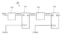
図5に、組合せ回路110、フリップフロップ111、組合せ回路112、フリップフロップ113を有する半導体装置120を示す。また図6に組合せ回路110、フリップフロップ111、組合せ回路112、フリップフロップ113、半導体装置115、半導体装置116を有する半導体装置125を示す。半導体装置115、116は図1(A)の半導体装置100と同様の構成を有する。なおフリップフロップ111、113、組合せ回路110、112は公知のものを用いることができる。
FIG. 5 illustrates a
半導体装置115はトランジスタ130及び回路131を有する。回路131は少なくともトランジスタ142を有する。
The
トランジスタ130のゲートには信号133が入力される。トランジスタ130のソース及びドレインの一方には信号134が入力される。トランジスタ130のソース及びドレインの他方はトランジスタ142のゲートに電気的に接続される。
A
回路131にはクロック信号1が入力され、タイミングが調節されたクロック信号150がフリップフロップ111に出力される。
The
半導体装置116はトランジスタ135及び回路136を有する。回路136は少なくともトランジスタ143を有する。
The
トランジスタ135のゲートには信号138が入力され、ソース及びドレインの一方には信号137が入力され、ソース及びドレインの他方はトランジスタ143のゲートに電気的に接続される。
A
回路136にはクロック信号2が入力され、タイミングが調節されたクロック信号151がフリップフロップ113に出力される。
The clock signal 2 is input to the
組合せ回路110にデータ1が入力され、データ2が出力される。フリップフロップ111にデータ2が入力され、データ3が出力される。組合せ回路112にデータ3が入力され、データ4が出力される。フリップフロップ113にデータ4が入力され、データ5が出力される。データ5は次の組合せ回路114(図示しない)に入力される。
図5に示す半導体装置120では、クロック信号1とクロック信号2のタイミング(t3)がずれ、さらに組合せ回路112によって生じる、フリップフロップ111からの出力(Q1)とフリップフロップ113への入力(D2)の遅延時間(t4)と大きく異なる場合がある。その結果、図7(A)ではt3+t4がクロックの1周期を超えてセットアップ違反が生じており、フリップフロップ113へ正常にデータ4が入力されていない。
In the
しかし図6に示す半導体装置125では、クロック信号のタイミングを調節できる。よって半導体装置116によりクロック信号2のタイミングをずらして小さくし、t3+t4<1周期とすることができる。その結果、フリップフロップ113へデータ4を正常に入力させることができる(図7(B))。
However, in the
また図5に示す半導体装置120では、クロック信号1とクロック信号2のタイミング(t6)がずれ、さらに組合せ回路112によって生じる、フリップフロップ111からの出力(Q1)とフリップフロップ113への入力(D2)の遅延時間(t7)と異なる場合がある。図8(A)ではt7<t6となり、ホールド違反が生じており、フリップフロップ113へ正常にデータ4が入力されていない。
In the
この場合、半導体装置116によりクロック信号2のタイミングをずらして、時間t8にロー信号からハイ信号に立ち上がるように調節することによりフリップフロップ113へ正常にデータ4を入力させることができる(図8(B))。
In this case, the data 4 can be normally input to the flip-
また半導体装置125を作成した後に、組合せ回路110、112などによって遅延時間が設計値と異なることがある。またクロック信号1とクロック信号2のタイミングのずれが設計値と異なることがある。これらは半導体装置125の誤動作につながる。しかし半導体装置125ではクロック信号150やクロック信号151を調節することができるから、半導体装置125に不具合が生じることはない。
Further, after the
(実施の形態2)
図9(A)に本発明の一態様である半導体装置200を示す。半導体装置200はトランジスタ201及びトランジスタ230を有する。
(Embodiment 2)
FIG. 9A illustrates a
トランジスタ201のゲートには信号203が入力され、信号203によりトランジスタ201のオン及びオフが制御される。トランジスタ201のソース及びドレインの一方には信号205が入力される。トランジスタ201のソース及びドレインの他方はトランジスタ230のゲートに電気的に接続される。
A
トランジスタ230のゲートに信号205に対応する電位が印加される。トランジスタ230のソース及びドレインの一方にはクロック信号206が入力される。トランジスタ230がオン状態のとき、トランジスタ230のソース及びドレインの他方からはクロック信号207が出力される。トランジスタ230はn型でもp型でもよい。以下では、トランジスタ230はn型として説明する。なおトランジスタ230はシリコン系半導体基板に設けてもよい。またトランジスタ230のチャネルが酸化物半導体層を有していてもよい。
A potential corresponding to the
トランジスタ230のId−Vg特性を図2に示す。信号205の電位(Vg)によって、Idは変化する(図2)。そうするとトランジスタ230は可変抵抗(R)とみなすことができる。トランジスタ230のId−Vg特性から、抵抗(R)を見積もることができる。
The Id-Vg characteristic of the
トランジスタ230のソース及びドレインの他方からは、クロック信号207が出力される。出力されたクロック信号207は、通常、例えばフリップフロップなどに含まれるトランジスタ239のゲートに入力される(図10)。
A
トランジスタ239のゲート容量(C)を考慮すると、クロック信号207の立ち上がりの時定数(τ)は、τ=RCで見積もることができる。なおRはトランジスタ230のId−Vg特性から決定される。
Considering the gate capacitance (C) of the
トランジスタ230を設けない場合には、図11(A)のように、ロー信号(L)からハイ信号(H)の切り替わりは図11(B)と比べて急峻である。クロック信号はt=0でローレベルからハイレベルに変わっている。
In the case where the
トランジスタ230を設けた場合には、図11(B)のように、時定数(τ)により、ロー信号(L)からハイ信号(H)の立ち上がりはなだらかになる。クロック信号はt=0でローレベルからなだらかに立ち上がり、t=t2でハイレベルに変わる。t2は信号205の電位に応じて変化させることができる。
When the
信号205によって、トランジスタ230のIdを変化させることができるから、時定数を変化させ、クロック信号207のタイミングを調節することができる。
Since the
なお図9(B)のように容量素子208を設けてもよい。ノード204の電位をより確実に保持することができる。
Note that a
半導体装置200の動作を説明する。
The operation of the
トランジスタ201に信号203が入力され、トランジスタ201がオンする。このときトランジスタ201のソース及びドレインの一方には信号205が入力され、トランジスタ230のゲートに入力される。信号205はクロック信号207のタイミングの調節量に応じたアナログ信号とすることができる。アナログ信号により微調整が可能である。
A
次に信号203によりトランジスタ201はオフする。トランジスタ201のオフ電流は極めて低いから、ノード204には信号205に対応した電位が保持され、トランジスタ230のゲートにも信号205に対応した電位が印加され続ける。クロック信号207のタイミングを調節する信号205をそのまま保存することができる。
Next, the
トランジスタ230には、クロック信号206が入力される。トランジスタ230は信号205の電位(Vg)によってIdが変化している。トランジスタ230からタイミングが調節されたクロック信号207が出力される。
A
図12に組合せ回路210、フリップフロップ211、組合せ回路212、フリップフロップ213、半導体装置241、半導体装置242を有する半導体装置240を示す。半導体装置241は、トランジスタ250、トランジスタ251を有する。半導体装置242は、トランジスタ254、トランジスタ255を有する。半導体装置241、242は図9(A)に示す半導体装置200と同様の構成を有する。なおフリップフロップ211、213は公知のものを用いることができる。また組合せ回路210、212は公知の回路を用いることができる。
FIG. 12 illustrates a
組合せ回路210にデータ1が入力され、データ2が出力される。フリップフロップ211にデータ2が入力され、データ3が出力される。組合せ回路212にデータ3が入力され、データ4が出力される。フリップフロップ213にデータ4が入力され、データ5が出力される。データ5は次の組合せ回路214(図示しない)に入力される。
トランジスタ250のゲートには信号252が入力される。トランジスタ250のソース及びドレインの一方には信号253が入力される。トランジスタ250のソース及びドレインの他方はトランジスタ251のゲートに電気的に接続される。トランジスタ251のソース及びドレインの一方にはクロック信号1が入力され、ソース及びドレインの他方からはタイミングが調節されたクロック信号260がフリップフロップ211に出力される。
A
トランジスタ254のゲートには信号256が入力され、ソース及びドレインの一方には信号257が入力され、ソース及びドレインの他方はトランジスタ255のゲートに電気的に接続される。トランジスタ255のソース及びドレインの一方にはクロック信号2が入力され、ソース及びドレインの他方からはタイミングが調節されたクロック信号261がフリップフロップ213に出力される。
A
半導体装置240は半導体装置241、半導体装置242を有している。よって実施の形態1で説明したように、クロック信号1とクロック信号2のタイミングの問題や、フリップフロップ211からの出力(Q1)とフリップフロップ213への入力(D2)の遅延時間の問題が生じても、クロック信号260、261のタイミングを調節することができ、半導体装置240を正常に動作させることができる。
The
(実施の形態3)
実施の形態2に示した半導体装置240ではクロック信号の時定数はフリップフロップ211、213のゲート容量(入力容量)に依存してしまう。ここではフリップフロップの入力容量に依存しない半導体装置を示す。図13に本発明の一態様である半導体装置300を示す。半導体装置300はトランジスタ301及び半導体装置320を有する。半導体装置320は実施の形態1の回路102に相当する。
(Embodiment 3)
In the
半導体装置320はインバータ313、トランジスタ330、インバータ314を有する。
The
トランジスタ301のゲートには信号303が入力される。トランジスタ301のソース及びドレインの一方には信号305が入力される。トランジスタ301のソース及びドレインの他方はトランジスタ330のゲートに電気的に接続される。
A
トランジスタ330のゲートに信号305に対応する電位(Vg)が印加される。トランジスタ330のソース及びドレインの一方にはインバータ313を介してクロック信号306が入力される。トランジスタ330のソース及びドレインの他方からはクロック信号312が出力され、インバータ314に入力される。インバータ314からクロック信号307が出力される。半導体装置320としては、クロック信号306が入力され、クロック信号307が出力される。
A potential (Vg) corresponding to the
なおトランジスタ330はn型でもp型でもよい。以下では、トランジスタ330はn型として説明する。なおトランジスタ330、インバータ313、インバータ314はシリコン系半導体基板に設けてもよい。またトランジスタ330のチャネルが形成される領域は酸化物半導体層を有していてもよい。
Note that the
インバータ313にはインバータ321からクロック信号306が入力されているが、インバータ321は必要に応じて設ければよい。
Although the
クロック信号307はフリップフロップ311に入力される。
The
なお容量素子308は必要に応じて設ければよい。容量素子308によりノード304の電位をより確実に保持することができる。
Note that the
トランジスタ330のIdは、信号305の電位(Vg)によって変化する。トランジスタ330から出力されるクロック信号312の時定数(τ)は、インバータ314を構成するトランジスタのゲート容量(C)に依存する。したがって半導体装置320だけで時定数を決定することができ、実施の形態2のようにフリップフロップ311のトランジスタのゲート容量(入力容量)に依存することなく、クロック信号307を調節することができる。
The Id of the
例えば、インバータ314を構成するトランジスタのゲート容量を適切に設定すると、信号305の電位(Vg)が小さいとき(Vg=Vg1のとき)は、クロック信号312は図14に示すようになだらかに立ち下がるようにすることができる。また信号305の電位(Vg)が大きいとき(Vg=Vg2のとき)は、クロック信号312は図14に示すように、Vg1よりも急峻に立ち下がるようにすることができる。
For example, when the gate capacitance of a transistor included in the
そしてインバータ314から出力されたクロック信号307をより遅くすること(Vg1)や、少し遅くすること(Vg2)ができる。
Then, the
半導体装置300の動作を説明する。
An operation of the
トランジスタ301に信号303が入力され、トランジスタ301がオンする。このときトランジスタ301のソース及びドレインの一方には信号305が入力され、トランジスタ330のゲートに入力される。信号305はクロック信号307のタイミングの調節量に応じたアナログ信号とすることができる。アナログ信号により微調整が可能である。
A
次に信号303によりトランジスタ301はオフする。トランジスタ301のオフ電流は極めて低いから、ノード304には信号305に対応した電位が保持され、トランジスタ330のゲートにも信号305に対応した電位が印加され続ける。クロック信号307のタイミングを調節する信号305をそのまま保存することができる。
Next, the
トランジスタ330には、インバータ313を介してクロック信号306が入力される。トランジスタ330は信号305の電位によってIdが変化している。上記したようにトランジスタ330からタイミングが調節されたクロック信号312が出力され、インバータ314に入力される。インバータ314からクロック信号307が出力される。
A
(実施の形態4)
図15に本発明の一態様である半導体装置400を示す。半導体装置400はトランジスタ401及び半導体装置420を有する。半導体装置420は実施の形態1の回路102に相当する。
(Embodiment 4)
FIG. 15 illustrates a
半導体装置420はインバータ413、トランジスタ430、インバータ414、容量素子418を有する。
The
トランジスタ401のゲートには信号403が入力される。トランジスタ401のソース及びドレインの一方には信号405が入力される。トランジスタ401のソース及びドレインの他方はトランジスタ430のゲートに電気的に接続される。
A
トランジスタ430のゲートに信号405に対応する電位が印加される。トランジスタ430のソース及びドレインの一方はインバータ413の出力に電気的に接続される。トランジスタ430のソース及びドレインの他方は容量素子418の一方の電極に電気的に接続される。
A potential corresponding to the
クロック信号406はインバータ413に入力される。インバータ413はクロック信号415を出力する。クロック信号415はインバータ414に入力される。インバータ414からクロック信号407が出力される。
The clock signal 406 is input to the
なおトランジスタ430はn型でもp型でもよい。以下では、トランジスタ430はn型として説明する。なおトランジスタ430、インバータ413、インバータ414はシリコン系半導体基板に設けてもよい。またトランジスタ430のチャネルが形成される領域は酸化物半導体層を有していてもよい。
Note that the
インバータ413にはインバータ421からクロック信号406が入力されているが、インバータ421は必要に応じて設ければよい。
Although the clock signal 406 is input to the
クロック信号407はフリップフロップ411に入力される。
The
なお容量素子408は必要に応じて設ければよい。容量素子408によりノード404の電位をより確実に保持することができる。
Note that the
トランジスタ430がオフのとき、クロック信号415はインバータ414に入力される。
When the
トランジスタ430がオンのとき、クロック信号415は、インバータ414だけでなく、トランジスタ430のソース及びドレインの一方にも入力される。そして容量素子418にも入力される。
When the
したがってトランジスタ430がオンのとき、インバータ413から出力されたクロック信号415の電荷は、インバータ414の入力容量だけでなく、トランジスタ430を介して容量素子418にも保持されていく。そうするとインバータ414がオンするまでの時間が遅れる。これによりクロック信号407のタイミングを調節することができる。
Therefore, when the
トランジスタ430のIdは、信号405の電位(Vg)によって変化する。トランジスタ430は可変抵抗(R)とみなすことができる。トランジスタ430の抵抗の大きさにより、容量素子418に保持される電荷を調節できる。そうするとインバータ414がオンするまでの時間を調節することができ、クロック信号407のタイミングを調節することができる。
The Id of the
半導体装置400の動作を説明する。
An operation of the
トランジスタ401に信号403が入力され、トランジスタ401がオンする。このときトランジスタ401のソース及びドレインの一方には信号405が入力され、トランジスタ430のゲートに入力される。信号405はクロック信号407のタイミングの調節量に応じたアナログ信号とすることができる。アナログ信号により微調整が可能である。
A
次に信号403によりトランジスタ401はオフする。トランジスタ401のオフ電流は極めて低いから、ノード404には信号405に対応した電位が保持され、トランジスタ430のゲートにも信号405に対応した電位が印加され続ける。クロック信号407のタイミングを調節する信号405をそのまま保存することができる。
Next, the
クロック信号406はインバータ413に入力される。インバータ413はクロック信号415を出力する。クロック信号415はインバータ414に入力され、トランジスタ430のソース及びドレインの一方にも入力され、容量素子418に入力される。このときトランジスタ430の抵抗にしたがって容量素子418に電荷が保持されていく。そうするとインバータ414がオンするまでの時間が遅れ、クロック信号407のタイミングを調節することができる。
The clock signal 406 is input to the
(実施の形態5)
図16に本発明の一態様である半導体装置500、501を示す。半導体装置500、501はそれぞれクロック信号を調節したいフリップフロップを選択できる。
(Embodiment 5)
FIG. 16 illustrates
半導体装置500は、組合せ回路510、フリップフロップ511、論理回路551、半導体装置515を有する。また半導体装置501は組合せ回路512、フリップフロップ513、論理回路552、半導体装置516を有する。
The
組合せ回路510にはデータ1が入力され、フリップフロップ511にデータ2が出力される。フリップフロップ511から組合せ回路512及び論理回路551にデータ3(信号553)が出力される。組合せ回路512からフリップフロップ513にデータ4が出力される。フリップフロップ513から次の組合せ回路514(図示しない)及び論理回路552にデータ(信号554)が出力される。
フリップフロップ511には半導体装置515からタイミングを調節されたクロック信号557が入力される。半導体装置515はトランジスタ530、半導体装置531を有する。半導体装置531は実施の形態1の回路102に相当する。
A
半導体装置531は少なくともトランジスタ542を有する。
The
トランジスタ530のゲートには論理回路551から信号555が入力される。トランジスタ530のソース及びドレインの一方には信号534が入力される。トランジスタ530のソース及びドレインの他方はトランジスタ542のゲートに電気的に接続される。
A
トランジスタ542のゲートに信号534に対応する電位が印加される。半導体装置531にはクロック信号1が入力され、タイミングが調節されたクロック信号557がフリップフロップ511に出力される。クロック信号557のタイミングを調節することについては実施の形態1−4にて説明したとおりである。
A potential corresponding to the
論理回路551には信号550及びフリップフロップ511から信号553が入力される。信号550及び信号553がともにハイ信号の場合には、信号555はハイ信号となり、トランジスタ530はオンとなる。信号550又は信号553の一方がロー信号の場合には、信号555はロー信号となり、トランジスタ530はオフとなる。
A
フリップフロップ513には半導体装置516からタイミングを調節されたクロック信号558が入力される。半導体装置516はトランジスタ535、半導体装置536を有する。半導体装置536は実施の形態1の回路102に相当する。
A
半導体装置536は少なくともトランジスタ543を有する。
The
トランジスタ535のゲートには論理回路552から信号556が入力される。トランジスタ535のソース及びドレインの一方には信号534が入力される。トランジスタ535のソース及びドレインの他方はトランジスタ543のゲートに電気的に接続される。信号534はトランジスタ530にも入力される。ここではトランジスタ530及びトランジスタ535の両方に信号534が入力されているが、トランジスタ530に入力される信号と異なる信号をトランジスタ535に入力してもよい。
A
トランジスタ543のゲートに信号534に対応する電位が印加される。半導体装置536にはクロック信号2が入力され、タイミングが調節されたクロック信号558がフリップフロップ513に出力される。クロック信号558のタイミングを調節することについては実施の形態1−4にて説明したとおりである。
A potential corresponding to the
論理回路552には信号550及びフリップフロップ513から信号554が入力される。信号550及び信号554がともにハイ信号の場合には、信号556はハイ信号となり、トランジスタ535はオンとなる。信号550又は信号554の一方がロー信号の場合には、信号556はロー信号となり、トランジスタ535はオフとなる。
A
ここで、特定のフリップフロップに入力されるクロック信号を調節する方法について説明する。通常のプロセッサにはスキャンチェインが実装されている。スキャンチェインは効果的に順序回路を試験する手法で、フリップフロップを直列につないで一種のシフトレジスタを構成したものである。専用ピンからそのシフトレジスタにシリアルデータを入力することによって、スキャンチェインに含まれる任意のフリップフロップの値を設定できるようになる。 Here, a method for adjusting a clock signal input to a specific flip-flop will be described. A normal processor has a scan chain. A scan chain is a method for effectively testing a sequential circuit, which is a type of shift register formed by connecting flip-flops in series. By inputting serial data from the dedicated pin to the shift register, the value of an arbitrary flip-flop included in the scan chain can be set.
フリップフロップ511に入力されるクロック信号557のみを調節するためには、スキャンチェインを用いて、フリップフロップ511の出力(Q1)を”1”に、他のフリップフロップ513の出力(Q2)を”0”に設定する。
In order to adjust only the
そして、信号550を制御すると、信号555は信号550と同じ振る舞いをし、信号556は常にロー信号(”0”)となる。つまり、トランジスタ530はオン・オフを制御できるが、トランジスタ535は常にオフとなる。
When the
このようにフリップフロップ511に入力されるクロック信号557のみを調節することができる。
In this way, only the
(実施の形態6)
実施の形態1−5のトランジスタのチャネルに適用できる酸化物半導体について説明する。
(Embodiment 6)
An oxide semiconductor that can be used for the channel of the transistor in Embodiment 1-5 is described.
電子供与体(ドナー)となる水分または水素などの不純物が低減され、なおかつ酸素欠損が低減されることにより高純度化された酸化物半導体(purified OS)は、i型(真性半導体)又はi型に限りなく近い。そのため、高純度化された酸化物半導体をチャネルに有するトランジスタは、オフ電流が著しく小さく、信頼性が高い。 An oxide semiconductor (purified OS) that is highly purified by reducing impurities such as moisture or hydrogen serving as an electron donor (donor) and reducing oxygen vacancies is i-type (intrinsic semiconductor) or i-type Infinitely close. Therefore, a transistor including a highly purified oxide semiconductor in a channel has extremely low off-state current and high reliability.
具体的に、高純度化された酸化物半導体をチャネルに有するトランジスタのオフ電流が小さいことは、いろいろな実験により証明できる。例えば、チャネル幅が1×106μmでチャネル長が10μmの素子であっても、ソース電極とドレイン電極間の電圧(ドレイン電圧)が1Vから10Vの範囲において、オフ電流が、半導体パラメータアナライザの測定限界以下、すなわち1×10⁻¹³A以下という特性を得ることができる。この場合、トランジスタのチャネル幅で規格化したオフ電流は、100zA/μm以下であることが分かる。また、容量素子とトランジスタとを接続して、容量素子に流入または容量素子から流出する電荷を当該トランジスタで制御する回路を用いて、オフ電流の測定を行った。当該測定では、高純度化された酸化物半導体膜を上記トランジスタのチャネル形成領域に用い、容量素子の単位時間あたりの電荷量の推移から当該トランジスタのオフ電流を測定した。その結果、トランジスタのソース電極とドレイン電極間の電圧が3Vの場合に、数十yA/μmという、さらに小さいオフ電流が得られることが分かった。従って、高純度化された酸化物半導体膜をチャネル形成領域に用いたトランジスタは、オフ電流が、結晶性を有するシリコンを用いたトランジスタに比べて著しく小さい。 Specifically, it can be proved by various experiments that the off-state current of a transistor including a highly purified oxide semiconductor in a channel is small. For example, even in an element having a channel width of 1 × 10 6 μm and a channel length of 10 μm, when the voltage between the source electrode and the drain electrode (drain voltage) is in the range of 1V to 10V, It is possible to obtain characteristics that are below the measurement limit, that is, 1 × 10 −13 A or less. In this case, it can be seen that the off-current normalized by the channel width of the transistor is 100 zA / μm or less. In addition, off-state current was measured using a circuit in which a capacitor and a transistor were connected and charge flowing into or out of the capacitor was controlled by the transistor. In this measurement, a highly purified oxide semiconductor film was used for a channel formation region of the transistor, and the off-state current of the transistor was measured from the change in charge amount per unit time of the capacitor. As a result, it was found that when the voltage between the source electrode and the drain electrode of the transistor is 3 V, an even smaller off current of several tens of yA / μm can be obtained. Therefore, a transistor using a highly purified oxide semiconductor film for a channel formation region has significantly lower off-state current than a transistor using crystalline silicon.
なお、特に断りがない限り、本明細書でオフ電流とは、nチャネル型トランジスタにおいては、ドレインをソースとゲートよりも高い電位とした状態において、ソースの電位を基準としたときのゲートの電位が0以下であるときに、ソースとドレインの間に流れる電流のことを意味する。或いは、本明細書でオフ電流とは、pチャネル型トランジスタにおいては、ドレインをソースとゲートよりも低い電位とした状態において、ソースの電位を基準としたときのゲートの電位が0以上であるときに、ソースとドレインの間に流れる電流のことを意味する。 Note that unless otherwise specified, off-state current in this specification refers to the gate potential when the drain potential is higher than that of the source and the gate in the n-channel transistor. It means a current that flows between the source and the drain when is less than or equal to zero. Alternatively, the off-state current in this specification refers to a p-channel transistor in which the potential of the gate is 0 or more with respect to the source potential in a state where the drain is at a lower potential than the source and the gate. In addition, it means a current flowing between the source and the drain.
酸化物半導体としては、少なくともインジウム(In)あるいは亜鉛(Zn)を含むことが好ましい。また、該酸化物半導体を用いたトランジスタの電気的特性のばらつきを減らすためのスタビライザーとして、それらに加えてガリウム(Ga)を有することが好ましい。また、スタビライザーとしてスズ(Sn)を有することが好ましい。また、スタビライザーとしてハフニウム(Hf)を有することが好ましい。また、スタビライザーとしてアルミニウム(Al)を有することが好ましい。また、スタビライザーとしてジルコニウム(Zr)を含むことが好ましい。 An oxide semiconductor preferably contains at least indium (In) or zinc (Zn). In addition, it is preferable that gallium (Ga) be included in addition to the stabilizer for reducing variation in electrical characteristics of the transistor including the oxide semiconductor. Moreover, it is preferable to have tin (Sn) as a stabilizer. Moreover, it is preferable to have hafnium (Hf) as a stabilizer. Moreover, it is preferable to have aluminum (Al) as a stabilizer. Moreover, it is preferable that zirconium (Zr) is included as a stabilizer.
酸化物半導体の中でもIn−Ga−Zn系酸化物、In−Sn−Zn系酸化物などは、炭化シリコン、窒化ガリウム、または酸化ガリウムとは異なり、スパッタリング法や湿式法により電気的特性の優れたトランジスタを作製することが可能であり、量産性に優れるといった利点がある。また、炭化シリコン、窒化ガリウム、または酸化ガリウムとは異なり、上記In−Ga−Zn系酸化物は、ガラス基板上に、電気的特性の優れたトランジスタを作製することが可能である。また、基板の大型化にも対応が可能である。 Among oxide semiconductors, In—Ga—Zn-based oxides, In—Sn—Zn-based oxides, and the like have excellent electrical characteristics by sputtering or a wet method, unlike silicon carbide, gallium nitride, or gallium oxide. There is an advantage that a transistor can be manufactured and the mass productivity is excellent. Further, unlike silicon carbide, gallium nitride, or gallium oxide, the In—Ga—Zn-based oxide can manufacture a transistor with excellent electrical characteristics over a glass substrate. Moreover, it is possible to cope with an increase in the size of the substrate.
また、他のスタビライザーとして、ランタノイドである、ランタン(La)、セリウム(Ce)、プラセオジム(Pr)、ネオジム(Nd)、サマリウム(Sm)、ユウロピウム(Eu)、ガドリニウム(Gd)、テルビウム(Tb)、ジスプロシウム(Dy)、ホルミウム(Ho)、エルビウム(Er)、ツリウム(Tm)、イッテルビウム(Yb)、ルテチウム(Lu)のいずれか一種または複数種を含んでいてもよい。 As other stabilizers, lanthanoids such as lanthanum (La), cerium (Ce), praseodymium (Pr), neodymium (Nd), samarium (Sm), europium (Eu), gadolinium (Gd), terbium (Tb) , Dysprosium (Dy), holmium (Ho), erbium (Er), thulium (Tm), ytterbium (Yb), or lutetium (Lu) may be included.
例えば、酸化物半導体として、酸化インジウム、酸化ガリウム、酸化スズ、酸化亜鉛、In−Zn系酸化物、Sn−Zn系酸化物、Al−Zn系酸化物、Zn−Mg系酸化物、Sn−Mg系酸化物、In−Mg系酸化物、In−Ga系酸化物、In−Ga−Zn系酸化物(IGZOとも表記する)、In−Al−Zn系酸化物、In−Sn−Zn系酸化物、Sn−Ga−Zn系酸化物、Al−Ga−Zn系酸化物、Sn−Al−Zn系酸化物、In−Hf−Zn系酸化物、In−La−Zn系酸化物、In−Pr−Zn系酸化物、In−Nd−Zn系酸化物、In−Sm−Zn系酸化物、In−Eu−Zn系酸化物、In−Gd−Zn系酸化物、In−Tb−Zn系酸化物、In−Dy−Zn系酸化物、In−Ho−Zn系酸化物、In−Er−Zn系酸化物、In−Tm−Zn系酸化物、In−Yb−Zn系酸化物、In−Lu−Zn系酸化物、In−Sn−Ga−Zn系酸化物、In−Hf−Ga−Zn系酸化物、In−Al−Ga−Zn系酸化物、In−Sn−Al−Zn系酸化物、In−Sn−Hf−Zn系酸化物、In−Hf−Al−Zn系酸化物を用いることができる。 For example, as an oxide semiconductor, indium oxide, gallium oxide, tin oxide, zinc oxide, In—Zn oxide, Sn—Zn oxide, Al—Zn oxide, Zn—Mg oxide, Sn—Mg Oxide, In—Mg oxide, In—Ga oxide, In—Ga—Zn oxide (also referred to as IGZO), In—Al—Zn oxide, In—Sn—Zn oxide Sn-Ga-Zn-based oxide, Al-Ga-Zn-based oxide, Sn-Al-Zn-based oxide, In-Hf-Zn-based oxide, In-La-Zn-based oxide, In-Pr- Zn-based oxide, In-Nd-Zn-based oxide, In-Sm-Zn-based oxide, In-Eu-Zn-based oxide, In-Gd-Zn-based oxide, In-Tb-Zn-based oxide, In-Dy-Zn-based oxide, In-Ho-Zn-based oxide, In-E -Zn-based oxide, In-Tm-Zn-based oxide, In-Yb-Zn-based oxide, In-Lu-Zn-based oxide, In-Sn-Ga-Zn-based oxide, In-Hf-Ga- A Zn-based oxide, an In-Al-Ga-Zn-based oxide, an In-Sn-Al-Zn-based oxide, an In-Sn-Hf-Zn-based oxide, or an In-Hf-Al-Zn-based oxide is used. be able to.
なお、例えば、In−Ga−Zn系酸化物とは、InとGaとZnを含む酸化物という意味であり、InとGaとZnの比率は問わない。また、InとGaとZn以外の金属元素を含んでいてもよい。In−Ga−Zn系酸化物は、無電界時の抵抗が十分に高くオフ電流を十分に小さくすることが可能であり、また、移動度も高い。 Note that for example, an In—Ga—Zn-based oxide means an oxide containing In, Ga, and Zn, and there is no limitation on the ratio of In, Ga, and Zn. Moreover, metal elements other than In, Ga, and Zn may be included. In-Ga-Zn-based oxides have sufficiently high resistance when no electric field is applied, and can have a sufficiently low off-state current, and also have high mobility.
例えば、In:Ga:Zn=1:1:1(=1/3:1/3:1/3)あるいはIn:Ga:Zn=2:2:1(=2/5:2/5:1/5)の原子比のIn−Ga−Zn系酸化物やその組成の近傍の酸化物を用いることができる。あるいは、In:Sn:Zn=1:1:1(=1/3:1/3:1/3)、In:Sn:Zn=2:1:3(=1/3:1/6:1/2)あるいはIn:Sn:Zn=2:1:5(=1/4:1/8:5/8)の原子比のIn−Sn−Zn系酸化物やその組成の近傍の酸化物を用いるとよい。 For example, In: Ga: Zn = 1: 1: 1 (= 1/3: 1/3: 1/3) or In: Ga: Zn = 2: 2: 1 (= 2/5: 2/5: 1). / 5) atomic ratio In—Ga—Zn-based oxides and oxides in the vicinity of the composition can be used. Alternatively, In: Sn: Zn = 1: 1: 1 (= 1/3: 1/3: 1/3), In: Sn: Zn = 2: 1: 3 (= 1/3: 1/6: 1) / 2) or In: Sn: Zn = 2: 1: 5 (= 1/4: 1/8: 5/8) atomic ratio In—Sn—Zn-based oxide or an oxide in the vicinity of the composition. Use it.
例えば、In−Sn−Zn系酸化物では比較的容易に高い移動度が得られる。しかしながら、In−Ga−Zn系酸化物でも、バルク内欠陥密度を低減することにより移動度を上げることができる。 For example, high mobility can be obtained relatively easily with an In—Sn—Zn-based oxide. However, mobility can be increased by reducing the defect density in the bulk also in the case of using an In—Ga—Zn-based oxide.
以下では、酸化物半導体膜の構造について説明する。 Hereinafter, the structure of the oxide semiconductor film is described.
酸化物半導体膜は、単結晶酸化物半導体膜と非単結晶酸化物半導体膜とに大別される。非単結晶酸化物半導体膜とは、非晶質酸化物半導体膜、微結晶酸化物半導体膜、多結晶酸化物半導体膜、CAAC−OS(C Axis Aligned Crystalline Oxide Semiconductor)膜などをいう。 An oxide semiconductor film is classified roughly into a single crystal oxide semiconductor film and a non-single crystal oxide semiconductor film. The non-single-crystal oxide semiconductor film refers to an amorphous oxide semiconductor film, a microcrystalline oxide semiconductor film, a polycrystalline oxide semiconductor film, a CAAC-OS (C Axis Crystalline Oxide Semiconductor) film, or the like.
非晶質酸化物半導体膜は、膜中における原子配列が不規則であり、結晶成分を有さない酸化物半導体膜である。微小領域においても結晶部を有さず、膜全体が完全な非晶質構造の酸化物半導体膜が典型である。 An amorphous oxide semiconductor film is an oxide semiconductor film having an irregular atomic arrangement in the film and having no crystal component. An oxide semiconductor film which has no crystal part even in a minute region and has a completely amorphous structure as a whole is typical.
微結晶酸化物半導体膜は、例えば、1nm以上10nm未満の大きさの微結晶(ナノ結晶ともいう。)を含む。従って、微結晶酸化物半導体膜は、非晶質酸化物半導体膜よりも原子配列の規則性が高い。そのため、微結晶酸化物半導体膜は、非晶質酸化物半導体膜よりも欠陥準位密度が低いという特徴がある。 The microcrystalline oxide semiconductor film includes a microcrystal (also referred to as nanocrystal) with a size greater than or equal to 1 nm and less than 10 nm, for example. Therefore, the microcrystalline oxide semiconductor film has higher regularity of atomic arrangement than the amorphous oxide semiconductor film. Therefore, a microcrystalline oxide semiconductor film has a feature that the density of defect states is lower than that of an amorphous oxide semiconductor film.
CAAC−OS膜は、複数の結晶部を有する酸化物半導体膜の一つであり、ほとんどの結晶部は、一辺が100nm未満の立方体内に収まる大きさである。従って、CAAC−OS膜に含まれる結晶部は、一辺が10nm未満、5nm未満または3nm未満の立方体内に収まる大きさの場合も含まれる。CAAC−OS膜は、微結晶酸化物半導体膜よりも欠陥準位密度が低いという特徴がある。以下、CAAC−OS膜について詳細な説明を行う。 The CAAC-OS film is one of oxide semiconductor films having a plurality of crystal parts, and most of the crystal parts are large enough to fit in a cube whose one side is less than 100 nm. Therefore, the case where a crystal part included in the CAAC-OS film fits in a cube whose one side is less than 10 nm, less than 5 nm, or less than 3 nm is included. The CAAC-OS film is characterized by having a lower density of defect states than a microcrystalline oxide semiconductor film. Hereinafter, the CAAC-OS film is described in detail.
CAAC−OS膜を透過型電子顕微鏡(TEM:Transmission Electron Microscope)によって観察すると、結晶部同士の明確な境界、即ち結晶粒界(グレインバウンダリーともいう。)を確認することができない。そのため、CAAC−OS膜は、結晶粒界に起因する電子移動度の低下が起こりにくいといえる。 When the CAAC-OS film is observed with a transmission electron microscope (TEM), a clear boundary between crystal parts, that is, a grain boundary (also referred to as a grain boundary) cannot be confirmed. Therefore, it can be said that the CAAC-OS film is unlikely to decrease in electron mobility due to crystal grain boundaries.
CAAC−OS膜を、試料面と概略平行な方向からTEMによって観察(断面TEM観察)すると、結晶部において、金属原子が層状に配列していることを確認できる。金属原子の各層は、CAAC−OS膜の膜を形成する面(被形成面ともいう。)または上面の凹凸を反映した形状であり、CAAC−OS膜の被形成面または上面と平行に配列する。 When the CAAC-OS film is observed by TEM (cross-sectional TEM observation) from a direction substantially parallel to the sample surface, it can be confirmed that metal atoms are arranged in layers in the crystal part. Each layer of metal atoms has a shape reflecting unevenness of a surface (also referred to as a formation surface) or an upper surface on which the CAAC-OS film is formed, and is arranged in parallel with the formation surface or the upper surface of the CAAC-OS film. .
一方、CAAC−OS膜を、試料面と概略垂直な方向からTEMによって観察(平面TEM観察)すると、結晶部において、金属原子が三角形状または六角形状に配列していることを確認できる。しかしながら、異なる結晶部間で、金属原子の配列に規則性は見られない。 On the other hand, when the CAAC-OS film is observed by TEM (planar TEM observation) from a direction substantially perpendicular to the sample surface, it can be confirmed that metal atoms are arranged in a triangular shape or a hexagonal shape in the crystal part. However, there is no regularity in the arrangement of metal atoms between different crystal parts.
断面TEM観察および平面TEM観察より、CAAC−OS膜の結晶部は配向性を有していることがわかる。 From the cross-sectional TEM observation and the planar TEM observation, it is found that the crystal part of the CAAC-OS film has orientation.
CAAC−OS膜に対し、X線回折(XRD:X−Ray Diffraction)装置を用いて構造解析を行うと、例えばInGaZnO4の結晶を有するCAAC−OS膜のout−of−plane法による解析では、回折角(2θ)が31°近傍にピークが現れる場合がある。このピークは、InGaZnO4の結晶の(009)面に帰属されることから、CAAC−OS膜の結晶がc軸配向性を有し、c軸が被形成面または上面に概略垂直な方向を向いていることが確認できる。 When structural analysis is performed on a CAAC-OS film using an X-ray diffraction (XRD) apparatus, for example, in the analysis of a CAAC-OS film having an InGaZnO 4 crystal by an out-of-plane method, A peak may appear when the diffraction angle (2θ) is around 31 °. Since this peak is attributed to the (009) plane of the InGaZnO 4 crystal, the CAAC-OS film crystal has c-axis orientation, and the c-axis is in a direction substantially perpendicular to the formation surface or the top surface. Can be confirmed.
一方、CAAC−OS膜に対し、c軸に概略垂直な方向からX線を入射させるin−plane法による解析では、2θが56°近傍にピークが現れる場合がある。このピークは、InGaZnO4の結晶の(110)面に帰属される。InGaZnO4の単結晶酸化物半導体膜であれば、2θを56°近傍に固定し、試料面の法線ベクトルを軸(φ軸)として試料を回転させながら分析(φスキャン)を行うと、(110)面と等価な結晶面に帰属されるピークが6本観察される。これに対し、CAAC−OS膜の場合は、2θを56°近傍に固定してφスキャンした場合でも、明瞭なピークが現れない。 On the other hand, when the CAAC-OS film is analyzed by an in-plane method in which X-rays are incident from a direction substantially perpendicular to the c-axis, a peak may appear when 2θ is around 56 °. This peak is attributed to the (110) plane of the InGaZnO 4 crystal. In the case of a single crystal oxide semiconductor film of InGaZnO 4 , when 2θ is fixed in the vicinity of 56 ° and analysis (φ scan) is performed while rotating the sample with the normal vector of the sample surface as the axis (φ axis), Six peaks attributed to the crystal plane equivalent to the (110) plane are observed. On the other hand, in the case of a CAAC-OS film, a peak is not clearly observed even when φ scan is performed with 2θ fixed at around 56 °.
以上のことから、CAAC−OS膜では、異なる結晶部間ではa軸およびb軸の配向は不規則であるが、c軸配向性を有し、かつc軸が被形成面または上面の法線ベクトルに平行な方向を向いていることがわかる。従って、前述の断面TEM観察で確認された層状に配列した金属原子の各層は、結晶のab面に平行な面である。 From the above, in the CAAC-OS film, the orientation of the a-axis and the b-axis is irregular between different crystal parts, but the c-axis is aligned, and the c-axis is a normal line of the formation surface or the top surface. It can be seen that the direction is parallel to the vector. Therefore, each layer of metal atoms arranged in a layer shape confirmed by the above-mentioned cross-sectional TEM observation is a plane parallel to the ab plane of the crystal.
なお、結晶部は、CAAC−OS膜を成膜した際、または加熱処理などの結晶化処理を行った際に形成される。上述したように、結晶のc軸は、CAAC−OS膜の被形成面または上面の法線ベクトルに平行な方向に配向する。従って、例えば、CAAC−OS膜の形状をエッチングなどによって変化させた場合、結晶のc軸がCAAC−OS膜の被形成面または上面の法線ベクトルと平行にならないこともある。 Note that the crystal part is formed when a CAAC-OS film is formed or when crystallization treatment such as heat treatment is performed. As described above, the c-axis of the crystal is oriented in a direction parallel to the normal vector of the formation surface or the top surface of the CAAC-OS film. Therefore, for example, when the shape of the CAAC-OS film is changed by etching or the like, the c-axis of the crystal may not be parallel to the normal vector of the formation surface or the top surface of the CAAC-OS film.
また、CAAC−OS膜中の結晶化度が均一でなくてもよい。例えば、CAAC−OS膜の結晶部が、CAAC−OS膜の上面近傍からの結晶成長によって形成される場合、上面近傍の領域は、被形成面近傍の領域よりも結晶化度が高くなることがある。また、CAAC−OS膜に不純物を添加する場合、不純物が添加された領域の結晶化度が変化し、部分的に結晶化度の異なる領域が形成されることもある。 Further, the crystallinity in the CAAC-OS film is not necessarily uniform. For example, in the case where the crystal part of the CAAC-OS film is formed by crystal growth from the vicinity of the top surface of the CAAC-OS film, the region near the top surface can have a higher degree of crystallinity than the region near the formation surface. is there. In addition, in the case where an impurity is added to the CAAC-OS film, the crystallinity of a region to which the impurity is added changes, and a region having a different degree of crystallinity may be formed.
なお、InGaZnO4の結晶を有するCAAC−OS膜のout−of−plane法による解析では、2θが31°近傍のピークの他に、2θが36°近傍にもピークが現れる場合がある。2θが36°近傍のピークは、CAAC−OS膜中の一部に、c軸配向性を有さない結晶が含まれることを示している。CAAC−OS膜は、2θが31°近傍にピークを示し、2θが36°近傍にピークを示さないことが好ましい。 Note that when the CAAC-OS film including an InGaZnO 4 crystal is analyzed by an out-of-plane method, a peak may also appear when 2θ is around 36 ° in addition to the peak where 2θ is around 31 °. A peak at 2θ of around 36 ° indicates that a crystal having no c-axis alignment is included in part of the CAAC-OS film. The CAAC-OS film preferably has a peak at 2θ of around 31 ° and no peak at 2θ of around 36 °.
CAAC−OS膜を用いたトランジスタは、可視光や紫外光の照射による電気特性の変動が小さい。よって、当該トランジスタは、信頼性が高い。 In a transistor using a CAAC-OS film, change in electrical characteristics due to irradiation with visible light or ultraviolet light is small. Therefore, the transistor has high reliability.
なお、酸化物半導体膜は、例えば、非晶質酸化物半導体膜、微結晶酸化物半導体膜、CAAC−OS膜のうち、二種以上を有する積層膜であってもよい。 Note that the oxide semiconductor film may be a stacked film including two or more of an amorphous oxide semiconductor film, a microcrystalline oxide semiconductor film, and a CAAC-OS film, for example.
CAAC−OS膜は、例えば、多結晶である金属酸化物ターゲットを用い、スパッタリング法によって成膜する。当該ターゲットにイオンが衝突すると、ターゲットに含まれる結晶領域がa−b面から劈開し、a−b面に平行な面を有する平板状またはペレット状のスパッタリング粒子として剥離することがある。この場合、当該平板状のスパッタリング粒子が、結晶状態を維持したまま基板に到達することで、CAAC−OS膜を成膜することができる。 The CAAC-OS film is formed by a sputtering method using a polycrystalline metal oxide target, for example. When ions collide with the target, a crystal region included in the target may be cleaved from the ab plane and separated as flat or pellet-like sputtered particles having a plane parallel to the ab plane. In this case, the flat-plate-like sputtered particle reaches the substrate while maintaining a crystalline state, whereby a CAAC-OS film can be formed.
また、CAAC−OS膜を成膜するために、以下の条件を適用することが好ましい。 In order to form the CAAC-OS film, the following conditions are preferably applied.
成膜時の不純物混入を低減することで、不純物によって結晶状態が崩れることを抑制できる。例えば、処理室内に存在する不純物濃度(水素、水、二酸化炭素、及び窒素など)を低減すればよい。また、成膜ガス中の不純物濃度を低減すればよい。具体的には、露点が−80℃以下、好ましくは−100℃以下である成膜ガスを用いる。 By reducing the mixing of impurities during film formation, the crystal state can be prevented from being broken by impurities. For example, the concentration of impurities (hydrogen, water, carbon dioxide, nitrogen, etc.) existing in the treatment chamber may be reduced. Further, the impurity concentration in the deposition gas may be reduced. Specifically, a deposition gas having a dew point of −80 ° C. or lower, preferably −100 ° C. or lower is used.
また、成膜時の基板加熱温度を高めることで、基板到達後にスパッタリング粒子のマイグレーションが起こる。具体的には、基板加熱温度を100℃以上740℃以下、好ましくは200℃以上500℃以下として成膜する。成膜時の基板加熱温度を高めることで、平板状のスパッタリング粒子が基板に到達した場合、基板上でマイグレーションが起こり、スパッタリング粒子の平らな面が基板に付着する。 Further, by increasing the substrate heating temperature during film formation, migration of sputtered particles occurs after reaching the substrate. Specifically, the film is formed at a substrate heating temperature of 100 ° C. to 740 ° C., preferably 200 ° C. to 500 ° C. By increasing the substrate heating temperature at the time of film formation, when the flat sputtered particles reach the substrate, migration occurs on the substrate, and the flat surface of the sputtered particles adheres to the substrate.
また、成膜ガス中の酸素割合を高め、電力を最適化することで成膜時のプラズマダメージを軽減すると好ましい。成膜ガス中の酸素割合は、30体積%以上、好ましくは100体積%とする。 In addition, it is preferable to reduce plasma damage during film formation by increasing the oxygen ratio in the film formation gas and optimizing electric power. The oxygen ratio in the deposition gas is 30% by volume or more, preferably 100% by volume.
ターゲットの一例として、In−Ga−Zn系酸化物ターゲットについて以下に示す。 As an example of the target, an In—Ga—Zn-based oxide target is described below.
InOX粉末、GaOY粉末及びZnOZ粉末を所定のmol数比で混合し、加圧処理後、1000℃以上1500℃以下の温度で加熱処理をすることで多結晶であるIn−Ga−Zn系酸化物ターゲットとする。なお、X、Y及びZは任意の正数である。ここで、所定のmol数比は、例えば、InOX粉末、GaOY粉末及びZnOZ粉末が、2:2:1、8:4:3、3:1:1、1:1:1、4:2:3または3:1:2である。なお、粉末の種類、及びその混合するmol数比は、作製するターゲットによって適宜変更すればよい。 In-Ga-Zn which is polycrystalline by mixing InO X powder, GaO Y powder and ZnO Z powder at a predetermined molar ratio, and after heat treatment at a temperature of 1000 ° C to 1500 ° C. A system oxide target is used. X, Y, and Z are arbitrary positive numbers. Here, the predetermined mole number ratio is, for example, 2: 2: 1, 8: 4: 3, 3: 1: 1, 1: 1: 1, 4 for InO X powder, GaO Y powder, and ZnO Z powder. : 2: 3 or 3: 1: 2. In addition, what is necessary is just to change suitably the kind of powder and the mol number ratio to mix with the target to produce.
なお、アルカリ金属は酸化物半導体を構成する元素ではないため、不純物である。アルカリ土類金属も、酸化物半導体を構成する元素ではない場合において、不純物となる。特に、アルカリ金属のうちNaは、酸化物半導体層に接する絶縁膜が酸化物である場合、当該絶縁膜中に拡散してNa+となる。また、Naは、酸化物半導体層内において、酸化物半導体を構成する金属と酸素の結合を分断する、或いは、その結合中に割り込む。その結果、例えば、閾値電圧がマイナス方向にシフトすることによるノーマリオン化、移動度の低下等の、トランジスタの電気的特性の劣化が起こり、加えて、特性のばらつきも生じる。具体的に、二次イオン質量分析法によるNa濃度の測定値は、5×10¹⁶/cm3以下、好ましくは1×1016/cm3以下、更に好ましくは1×1015/cm3以下とするとよい。同様に、Li濃度の測定値は、5×1015/cm3以下、好ましくは1×1015/cm3以下とするとよい。同様に、K濃度の測定値は、5×1015/cm3以下、好ましくは1×1015/cm3以下とするとよい。 Note that an alkali metal is an impurity because it is not an element included in an oxide semiconductor. Alkaline earth metal is also an impurity when it is not an element constituting an oxide semiconductor. In particular, Na in the alkali metal diffuses into the insulating film and becomes Na + when the insulating film in contact with the oxide semiconductor layer is an oxide. In the oxide semiconductor layer, Na breaks or interrupts the bond between the metal and the oxygen included in the oxide semiconductor. As a result, for example, the transistor is deteriorated in electrical characteristics, such as being normally on due to the shift of the threshold voltage in the negative direction, and a decrease in mobility. In addition, the characteristics vary. Specifically, the measured value of Na concentration by secondary ion mass spectrometry is 5 × 10 16 / cm 3 or less, preferably 1 × 10 16 / cm 3 or less, more preferably 1 × 10 15 / cm 3 or less. Good. Similarly, the measured value of the Li concentration is 5 × 10 15 / cm 3 or less, preferably 1 × 10 15 / cm 3 or less. Similarly, the measured value of the K concentration is 5 × 10 15 / cm 3 or less, preferably 1 × 10 15 / cm 3 or less.
また、インジウムを含む金属酸化物が用いられている場合に、酸素との結合エネルギーがインジウムよりも大きいシリコンや炭素が、インジウムと酸素の結合を切断し、酸素欠損を形成することがある。そのため、シリコンや炭素が酸化物半導体層に混入していると、アルカリ金属やアルカリ土類金属の場合と同様に、トランジスタの電気的特性の劣化が起こりやすい。よって、酸化物半導体層中におけるシリコンや炭素の濃度は低いことが望ましい。具体的に、二次イオン質量分析法によるC濃度の測定値、またはSi濃度の測定値は、1×10¹⁸/cm3以下とするとよい。上記構成により、トランジスタの電気的特性の劣化を防ぐことができ、半導体装置の信頼性を高めることができる。 In addition, in the case where a metal oxide containing indium is used, silicon or carbon whose binding energy to oxygen is higher than that of indium may cut the bond between indium and oxygen, thereby forming an oxygen vacancy. Therefore, when silicon or carbon is mixed in the oxide semiconductor layer, the electrical characteristics of the transistor are likely to deteriorate as in the case of alkali metal or alkaline earth metal. Therefore, it is desirable that the concentration of silicon or carbon in the oxide semiconductor layer be low. Specifically, the measured value of C concentration or the measured value of Si concentration by secondary ion mass spectrometry is preferably 1 × 10 18 / cm 3 or less. With the above structure, deterioration of electrical characteristics of the transistor can be prevented, and reliability of the semiconductor device can be improved.
また、ソース電極及びドレイン電極に用いられる導電性材料によっては、ソース電極及びドレイン電極中の金属が、酸化物半導体膜から酸素を引き抜くことがある。この場合、酸化物半導体層のうち、ソース電極及びドレイン電極に接する領域が、酸素欠損の形成によりn型化される。 Further, depending on the conductive material used for the source electrode and the drain electrode, the metal in the source electrode and the drain electrode might extract oxygen from the oxide semiconductor film. In this case, a region in contact with the source electrode and the drain electrode in the oxide semiconductor layer is n-type due to formation of oxygen vacancies.
n型化された領域は、ソース領域またはドレイン領域として機能するため、酸化物半導体膜とソース電極及びドレイン電極との間におけるコンタクト抵抗を下げることができる。よって、n型化された領域が形成されることで、トランジスタの移動度及びオン電流を高めることができ、それにより、トランジスタを用いたスイッチ回路の高速動作を実現することができる。 Since the n-type region functions as a source region or a drain region, contact resistance between the oxide semiconductor film and the source and drain electrodes can be reduced. Thus, by forming an n-type region, the mobility and on-state current of the transistor can be increased, whereby high-speed operation of the switch circuit using the transistor can be realized.
なお、ソース電極及びドレイン電極中の金属による酸素の引き抜きは、ソース電極及びドレイン電極をスパッタリング法などにより形成する際に起こりうるし、ソース電極及びドレイン電極を形成した後に行われる加熱処理によっても起こりうる。 Note that extraction of oxygen by a metal in the source electrode and the drain electrode can occur when the source electrode and the drain electrode are formed by a sputtering method or the like, and can also occur by a heat treatment performed after the source electrode and the drain electrode are formed. .
また、n型化される領域は、酸素と結合し易い導電性材料をソース電極及びドレイン電極に用いることで、より形成されやすくなる。上記導電性材料としては、例えば、Al、Cr、Cu、Ta、Ti、Mo、Wなどが挙げられる。 In addition, the n-type region is more easily formed by using a conductive material that is easily bonded to oxygen for the source electrode and the drain electrode. Examples of the conductive material include Al, Cr, Cu, Ta, Ti, Mo, and W.
また、酸化物半導体層は、単数の金属酸化物膜で構成されているとは限らず、積層された複数の金属酸化物膜で構成されていても良い。例えば、第1乃至第3の金属酸化物膜が順に積層されている半導体膜の場合、第1の金属酸化物膜及び第3の金属酸化物膜は、第2の金属酸化物膜を構成する金属元素の少なくとも1つを、その構成要素に含み、伝導帯下端のエネルギーが第2の金属酸化物膜よりも0.05eV以上、0.07eV以上、0.1eV以上または0.15eV以上、かつ2eV以下、1eV以下、0.5eV以下または0.4eV以下、真空準位に近い酸化物膜である。さらに、第2の金属酸化物膜は、少なくともインジウムを含むと、キャリア移動度が高くなるため好ましい。 In addition, the oxide semiconductor layer is not necessarily composed of a single metal oxide film, and may be composed of a plurality of stacked metal oxide films. For example, in the case of a semiconductor film in which first to third metal oxide films are sequentially stacked, the first metal oxide film and the third metal oxide film constitute a second metal oxide film. At least one metal element is included in the component, and the energy at the lower end of the conduction band is 0.05 eV or more, 0.07 eV or more, 0.1 eV or more, or 0.15 eV or more than the second metal oxide film, and 2eV or less, 1eV or less, 0.5eV or less, or 0.4eV or less, which is an oxide film close to a vacuum level. Furthermore, it is preferable that the second metal oxide film contains at least indium because carrier mobility is increased.
上記構成の半導体膜をトランジスタが有する場合、ゲート電極に電圧を印加することで、半導体膜に電界が加わると、半導体膜のうち、伝導帯下端のエネルギーが小さい第2の金属酸化物膜にチャネル領域が形成される。即ち、第2の金属酸化物膜とゲート絶縁膜との間に第3の金属酸化物膜が設けられていることによって、ゲート絶縁膜と離隔している第2の金属酸化物膜に、チャネル領域を形成することができる。 In the case where the transistor includes the semiconductor film having the above structure, when an electric field is applied to the semiconductor film by applying a voltage to the gate electrode, a channel is formed in the second metal oxide film having a lower conduction band energy in the semiconductor film. A region is formed. That is, since the third metal oxide film is provided between the second metal oxide film and the gate insulating film, the second metal oxide film separated from the gate insulating film has a channel. Regions can be formed.
また、第3の金属酸化物膜は、第2の金属酸化物膜を構成する金属元素の少なくとも1つをその構成要素に含むため、第2の金属酸化物膜と第3の金属酸化物膜の界面では、界面散乱が起こりにくい。従って、当該界面においてキャリアの動きが阻害されにくいため、トランジスタの電界効果移動度が高くなる。 In addition, since the third metal oxide film includes at least one of the metal elements constituting the second metal oxide film in its constituent elements, the second metal oxide film and the third metal oxide film Interface scattering is unlikely to occur at the interface. Accordingly, since the movement of carriers at the interface is difficult to be inhibited, the field effect mobility of the transistor is increased.
また、第2の金属酸化物膜と第1の金属酸化物膜の界面に界面準位が形成されると、界面近傍の領域にもチャネル領域が形成されるために、トランジスタの閾値電圧が変動してしまう。しかし、第1の金属酸化物膜は、第2の金属酸化物膜を構成する金属元素の少なくとも1つをその構成要素に含むため、第2の金属酸化物膜と第1の金属酸化物膜の界面には、界面準位が形成されにくい。よって、上記構成により、トランジスタの閾値電圧等の電気的特性のばらつきを、低減することができる。 In addition, when an interface state is formed at the interface between the second metal oxide film and the first metal oxide film, a channel region is also formed in a region near the interface, so that the threshold voltage of the transistor fluctuates. Resulting in. However, since the first metal oxide film includes at least one of the metal elements constituting the second metal oxide film in its constituent elements, the second metal oxide film and the first metal oxide film It is difficult to form interface states at the interface. Thus, with the above structure, variation in electrical characteristics such as threshold voltage of the transistor can be reduced.
また、金属酸化物膜間に不純物が存在することによって、各膜の界面にキャリアの流れを阻害する界面準位が形成されることがないよう、複数の金属酸化物膜を積層させることが望ましい。積層された金属酸化物膜の膜間に不純物が存在していると、金属酸化物膜間における伝導帯下端のエネルギーの連続性が失われ、界面近傍において、キャリアがトラップされるか、あるいは再結合により消滅してしまうからである。膜間における不純物を低減させることで、主成分である一の金属を少なくとも共に有する複数の金属酸化物膜を、単に積層させるよりも、連続接合(ここでは特に伝導帯下端のエネルギーが各膜の間で連続的に変化するU字型の井戸構造を有している状態)が形成されやすくなる。 In addition, it is desirable to stack a plurality of metal oxide films so that the presence of impurities between the metal oxide films does not form an interface state that inhibits the flow of carriers at the interface of each film. . If impurities exist between the stacked metal oxide films, the continuity of the energy at the bottom of the conduction band between the metal oxide films is lost, and carriers are trapped or re-entered near the interface. This is because the bonds disappear. By reducing the impurities between the films, a plurality of metal oxide films having at least one metal as a main component together are not simply stacked. A state of having a U-shaped well structure that continuously changes between them).
連続接合を形成するためには、ロードロック室を備えたマルチチャンバー方式の成膜装置(スパッタリング装置)を用いて各膜を大気に触れさせることなく連続して積層することが必要となる。スパッタリング装置における各チャンバーは、酸化物半導体にとって不純物となる水等を可能な限り除去すべくクライオポンプのような吸着式の真空排気ポンプを用いて高真空排気(5×10⁻⁷Pa〜1×10⁻⁴Pa程度まで)することが好ましい。または、ターボ分子ポンプとコールドトラップを組み合わせて排気系からチャンバー内に気体が逆流しないようにしておくことが好ましい。 In order to form a continuous bond, it is necessary to use a multi-chamber type film forming apparatus (sputtering apparatus) provided with a load lock chamber to continuously laminate each film without exposure to the atmosphere. Each chamber in the sputtering apparatus is evacuated (5 × 10 −7 Pa to 1 ×) using an adsorption-type evacuation pump such as a cryopump so as to remove as much water as possible from the oxide semiconductor. It is preferable to be up to about 10 −4 Pa. Alternatively, it is preferable to combine a turbo molecular pump and a cold trap so that gas does not flow backward from the exhaust system into the chamber.
高純度の真性な酸化物半導体を得るためには、各チャンバー内を高真空排気するのみならず、スパッタリングに用いるガスの高純度化も重要である。上記ガスとして用いる酸素ガスやアルゴンガスの露点を、−40℃以下、好ましくは−80℃以下、より好ましくは−100℃以下とし、使用するガスの高純度化を図ることで、酸化物半導体膜に水分等が取り込まれることを可能な限り防ぐことができる。 In order to obtain a high-purity intrinsic oxide semiconductor, it is important not only to evacuate each chamber to a high vacuum but also to increase the purity of a gas used for sputtering. The dew point of oxygen gas or argon gas used as the gas is −40 ° C. or lower, preferably −80 ° C. or lower, more preferably −100 ° C. or lower, and the oxide semiconductor film is made highly purified by purifying the gas used. It is possible to prevent moisture and the like from being taken into the body as much as possible.
例えば、第1の金属酸化物膜または第3の金属酸化物膜は、アルミニウム、シリコン、チタン、ガリウム、ゲルマニウム、イットリウム、ジルコニウム、スズ、ランタン、セリウムまたはハフニウムを、第2の金属酸化物膜よりも高い原子数比で含む酸化物膜であればよい。具体的に、第1の金属酸化物膜または第3の金属酸化物膜として、第2の金属酸化物膜よりも上述の元素を1.5倍以上、好ましくは2倍以上、さらに好ましくは3倍以上高い原子数比で含む酸化物膜を用いると良い。前述の元素は酸素と強く結合するため、酸素欠損が酸化物膜に生じることを抑制する機能を有する。よって、上記構成により、第1の金属酸化物膜または第3の金属酸化物膜を、第2の金属酸化物膜よりも酸素欠損が生じにくい酸化物膜にすることができる。 For example, the first metal oxide film or the third metal oxide film is formed using aluminum, silicon, titanium, gallium, germanium, yttrium, zirconium, tin, lanthanum, cerium, or hafnium more than the second metal oxide film. As long as the oxide film contains a high atomic ratio. Specifically, as the first metal oxide film or the third metal oxide film, the above-described element is 1.5 times or more, preferably 2 times or more than the second metal oxide film, more preferably 3 times or more. An oxide film including an atomic ratio which is twice or more higher is preferably used. The above element is strongly bonded to oxygen and thus has a function of suppressing generation of oxygen vacancies in the oxide film. Therefore, with the above structure, the first metal oxide film or the third metal oxide film can be an oxide film in which oxygen vacancies are less likely to be generated than in the second metal oxide film.
具体的に、第2の金属酸化物膜と、第1の金属酸化物膜または第3の金属酸化物膜とが、共にIn−M−Zn系酸化物である場合、第1の金属酸化物膜または第3の金属酸化物膜の原子数比をIn:M:Zn=x1:y1:z1、第2の金属酸化物膜の原子数比をIn:M:Zn=x2:y2:z2とすると、y1/x1がy2/x2よりも大きくなるように、その原子数比を設定すれば良い。なお、元素MはInよりも酸素との結合力が強い金属元素であり、例えばAl、Ti、Ga、Y、Zr、Sn、La、Ce、NdまたはHf等が挙げられる。好ましくは、y1/x1がy2/x2よりも1.5倍以上大きくなるように、その原子数比を設定すれば良い。さらに好ましくは、y1/x1がy2/x2よりも2倍以上大きくなるように、その原子数比を設定すれば良い。より好ましくは、y1/x1がy2/x2よりも3倍以上大きくなるように、その原子数比を設定すれば良い。さらに、第2の金属酸化物膜において、y2がx2以上であると、トランジスタに安定した電気的特性を付与できるため好ましい。ただし、y2がx2の3倍以上になると、トランジスタの電界効果移動度が低下してしまうため、y2はx2の3倍未満であると好ましい。 Specifically, when the second metal oxide film and the first metal oxide film or the third metal oxide film are both In-M-Zn-based oxides, the first metal oxide film The atomic ratio of the film or the third metal oxide film is In: M: Zn = x 1 : y 1 : z 1 , and the atomic ratio of the second metal oxide film is In: M: Zn = x 2 : If y 2 : z 2 , the atomic ratio may be set so that y 1 / x 1 is larger than y 2 / x 2 . Note that the element M is a metal element having a stronger bonding force with oxygen than In, and examples thereof include Al, Ti, Ga, Y, Zr, Sn, La, Ce, Nd, and Hf. Preferably, the atomic ratio may be set so that y 1 / x 1 is 1.5 times or more larger than y 2 / x 2 . More preferably, the atomic ratio may be set so that y 1 / x 1 is twice or more larger than y 2 / x 2 . More preferably, the atomic ratio may be set so that y 1 / x 1 is three times or more larger than y 2 / x 2 . Furthermore, in the second metal oxide film, it is preferable that y 2 is x 2 or more because stable electrical characteristics can be imparted to the transistor. However, when y 2 is 3 times or more of x 2 , the field-effect mobility of the transistor is lowered. Therefore, y 2 is preferably less than 3 times x 2 .
なお、第1の金属酸化物膜及び第3の金属酸化物膜の厚さは、3nm以上100nm以下、好ましくは3nm以上50nm以下とする。また、第2の金属酸化物膜の厚さは、3nm以上200nm以下、好ましくは3nm以上100nm以下であり、さらに好ましくは3nm以上50nm以下である。 Note that the thicknesses of the first metal oxide film and the third metal oxide film are 3 nm to 100 nm, preferably 3 nm to 50 nm. The thickness of the second metal oxide film is 3 nm to 200 nm, preferably 3 nm to 100 nm, and more preferably 3 nm to 50 nm.
3層構造の半導体膜において、第1の金属酸化物膜乃至第3の金属酸化物膜は、非晶質または結晶質の両方の形態を取りうる。ただし、チャネル領域が形成される第2の金属酸化物膜が結晶質であることにより、トランジスタに安定した電気的特性を付与することができるため、第2の金属酸化物膜は結晶質であることが好ましい。 In the semiconductor film having a three-layer structure, the first metal oxide film to the third metal oxide film can take either amorphous or crystalline forms. However, since the second metal oxide film in which the channel region is formed is crystalline, stable electrical characteristics can be given to the transistor, and thus the second metal oxide film is crystalline. It is preferable.
なお、チャネル形成領域とは、トランジスタの半導体膜のうち、ゲート電極と重なり、かつソース電極とドレイン電極に挟まれる領域を意味する。また、チャネル領域とは、チャネル形成領域において、電流が主として流れる領域をいう。 Note that a channel formation region means a region of a semiconductor film of a transistor that overlaps with a gate electrode and is sandwiched between a source electrode and a drain electrode. The channel region refers to a region where current mainly flows in the channel formation region.
例えば、第1の金属酸化物膜及び第3の金属酸化物膜として、スパッタリング法により形成したIn−Ga−Zn系酸化物膜を用いる場合、第1の金属酸化物膜及び第3の金属酸化物膜の成膜には、In−Ga−Zn系酸化物(In:Ga:Zn=1:3:2[原子数比])であるターゲットを用いることができる。成膜条件は、例えば、成膜ガスとしてアルゴンガスを30sccm、酸素ガスを15sccm用い、圧力0.4Paとし、基板温度を200℃とし、DC電力0.5kWとすればよい。 For example, when an In—Ga—Zn-based oxide film formed by a sputtering method is used as the first metal oxide film and the third metal oxide film, the first metal oxide film and the third metal oxide film are used. For the formation of the physical film, a target that is an In—Ga—Zn-based oxide (In: Ga: Zn = 1: 3: 2 [atomic ratio]) can be used. The film forming conditions may be, for example, 30 sccm of argon gas and 15 sccm of oxygen gas, a pressure of 0.4 Pa, a substrate temperature of 200 ° C., and a DC power of 0.5 kW.
また、第2の金属酸化物膜をCAAC−OS膜とする場合、第2の金属酸化物膜の成膜には、In−Ga−Zn系酸化物(In:Ga:Zn=1:1:1[原子数比])であり、多結晶のIn−Ga−Zn系酸化物を含むターゲットを用いることが好ましい。成膜条件は、例えば、成膜ガスとしてアルゴンガスを30sccm、酸素ガスを15sccm用い、圧力を0.4Paとし、基板の温度300℃とし、DC電力0.5kWとすることができる。 In the case where the second metal oxide film is a CAAC-OS film, an In—Ga—Zn-based oxide (In: Ga: Zn = 1: 1: 1 [atomic ratio]) and a target including a polycrystalline In—Ga—Zn-based oxide is preferably used. The film forming conditions may be, for example, an argon gas of 30 sccm and an oxygen gas of 15 sccm as a film forming gas, a pressure of 0.4 Pa, a substrate temperature of 300 ° C., and a DC power of 0.5 kW.
なお、トランジスタは、半導体膜の端部が傾斜している構造を有していても良いし、半導体膜の端部が丸みを帯びる構造を有していても良い。 Note that the transistor may have a structure in which an end portion of the semiconductor film is inclined or a structure in which an end portion of the semiconductor film is rounded.
また、複数の積層された金属酸化物膜を有する半導体膜をトランジスタに用いる場合においても、ソース電極及びドレイン電極に接する領域が、n型化されていても良い。上記構成により、トランジスタの移動度及びオン電流を高め、半導体装置の高速動作を実現することができる。さらに、複数の積層された金属酸化物膜を有する半導体膜をトランジスタに用いる場合、n型化される領域は、チャネル領域となる第2の金属酸化物膜にまで達していることが、トランジスタの移動度及びオン電流を高め、半導体装置のさらなる高速動作を実現する上で、より好ましい。 In the case where a semiconductor film including a plurality of stacked metal oxide films is used for a transistor, regions in contact with the source electrode and the drain electrode may be n-type. With the above structure, the mobility and on-state current of the transistor can be increased and high-speed operation of the semiconductor device can be realized. Further, in the case where a semiconductor film including a plurality of stacked metal oxide films is used for a transistor, the n-type region reaches the second metal oxide film serving as a channel region. It is more preferable in increasing mobility and on-current and realizing further high-speed operation of the semiconductor device.
(実施の形態7)
実施の形態1−5に示した半導体装置の一例について説明する。図17に、図1(B)に示した半導体装置100が有する、トランジスタ101、トランジスタ141、及び容量素子108の断面構造を、一例として示す。
(Embodiment 7)
An example of the semiconductor device described in Embodiment 1-5 will be described. FIG. 17 illustrates an example of a cross-sectional structure of the
トランジスタ101のチャネルは酸化物半導体層を有している。トランジスタ101、容量素子108が、単結晶のシリコン基板にチャネル形成領域を有するトランジスタ141上に形成されている場合を例示している。
The channel of the
なお、トランジスタ141は、非晶質、微結晶、多結晶または単結晶である、シリコン又はゲルマニウムなどの半導体膜を活性層に用いることもできる。或いは、トランジスタ141は、酸化物半導体を活性層に用いていても良い。全てのトランジスタが酸化物半導体を活性層に用いている場合、トランジスタ101はトランジスタ141上に積層されていなくとも良く、トランジスタ101とトランジスタ141とは、同一の層に形成されていても良い。
Note that the
薄膜のシリコンを用いてトランジスタ141を形成する場合、プラズマCVD法などの気相成長法若しくはスパッタリング法で作製された非晶質シリコン、非晶質シリコンにレーザー光を照射して結晶化させた多結晶シリコン、単結晶シリコンウェハに水素イオン等を注入して表層部を剥離した単結晶シリコンなどを用いることができる。
In the case where the
トランジスタ141が形成される半導体基板1400は、例えば、n型またはp型の導電型を有するシリコン基板、ゲルマニウム基板、シリコンゲルマニウム基板、化合物半導体基板(GaAs基板、InP基板、GaN基板、SiC基板、GaP基板、GaInAsP基板、ZnSe基板等)等を用いることができる。図17では、n型の導電性を有する単結晶シリコン基板を用いた場合を例示している。
The
また、トランジスタ141は、素子分離用絶縁膜1401により、他のトランジスタと、電気的に分離されている。素子分離用絶縁膜1401の形成には、選択酸化法(LOCOS(Local Oxidation of Silicon)法)またはトレンチ分離法等を用いることができる。
The
具体的に、トランジスタ141は、半導体基板1400に形成された、ソース領域またはドレイン領域として機能する不純物領域1402及び不純物領域1403と、ゲート電極1404と、半導体基板1400とゲート電極1404の間に設けられたゲート絶縁膜1405とを有する。ゲート電極1404は、ゲート絶縁膜1405を間に挟んで、不純物領域1402と不純物領域1403の間に形成されるチャネル形成領域と重なる。
Specifically, the
トランジスタ141上には、絶縁膜1409が設けられている。絶縁膜1409には開口部が形成されている。そして、上記開口部には、不純物領域1402、不純物領域1403にそれぞれ接する配線1410、配線1411と、ゲート電極1404に電気的に接続されている配線1412とが、形成されている。
An insulating
そして、配線1410は、絶縁膜1409上に形成された配線1415に電気的に接続されており、配線1411は、絶縁膜1409上に形成された配線1416に電気的に接続されており、配線1412は、絶縁膜1409上に形成された配線1417に電気的に接続されている。
The
配線1415乃至配線1417上には、絶縁膜1420及び絶縁膜1440が順に積層するように形成されている。絶縁膜1420及び絶縁膜1440には開口部が形成されており、上記開口部に、配線1417に電気的に接続された配線1421が形成されている。
Over the
そして、図17では、絶縁膜1440上にトランジスタ101及び容量素子108が形成されている。
In FIG. 17, the
トランジスタ101は、絶縁膜1440上に、酸化物半導体を含む半導体膜1430と、半導体膜1430上の、ソース電極またはドレイン電極として機能する導電膜1432及び導電膜1433と、半導体膜1430、導電膜1432及び導電膜1433上のゲート絶縁膜1431と、ゲート絶縁膜1431上に位置し、導電膜1432と導電膜1433の間において半導体膜1430と重なっているゲート電極1434と、を有する。なお、導電膜1433は、配線1421に電気的に接続されている。
The
また、ゲート絶縁膜1431上において導電膜1433と重なる位置に、導電膜1435が設けられている。ゲート絶縁膜1431を間に挟んで導電膜1433及び導電膜1435が重なっている部分が、容量素子108として機能する。
A
なお、図17では、容量素子108がトランジスタ101と共に絶縁膜1440の上に設けられている場合を例示しているが、容量素子108は、トランジスタ141と共に、絶縁膜1440の下に設けられていても良い。
Note that FIG. 17 illustrates the case where the
そして、トランジスタ101、容量素子108上に、絶縁膜1441及び絶縁膜1442が順に積層するように設けられている。絶縁膜1441及び絶縁膜1442には開口部が設けられており、上記開口部においてゲート電極1434に接する導電膜1443が、絶縁膜1441上に設けられている。
An insulating
なお、図17において、トランジスタ101は、ゲート電極1434を半導体膜1430の片側において少なくとも有していれば良いが、半導体膜1430を間に挟んで存在する一対のゲート電極を有していても良い。
Note that in FIG. 17, the
トランジスタ101が、半導体膜1430を間に挟んで存在する一対のゲート電極を有している場合、一方のゲート電極には導通状態または非導通状態を制御するための信号が与えられ、他方のゲート電極は、電位が他から与えられている状態であっても良い。この場合、一対のゲート電極に、同じ高さの電位が与えられていても良いし、他方のゲート電極にのみ接地電位などの固定の電位が与えられていても良い。他方のゲート電極に与える電位の高さを制御することで、トランジスタの閾値電圧を制御することができる。
In the case where the
また、図17では、トランジスタ101が、一のゲート電極1434に対応した一のチャネル形成領域を有する、シングルゲート構造である場合を例示している。しかし、トランジスタ101は、電気的に接続された複数のゲート電極を有することで、一の活性層にチャネル形成領域を複数有する、マルチゲート構造であっても良い。
FIG. 17 illustrates the case where the
(実施の形態8)
本実施の形態では、本発明の一態様に係る半導体装置の一つである、CPUの構成について説明する。
(Embodiment 8)
In this embodiment, a structure of a CPU that is one of semiconductor devices according to one embodiment of the present invention will be described.
図18に、本実施の形態のCPUの構成を示す。図18に示すCPUは、基板900上に、演算回路(ALU:Arithmetic logic unit)901、ALU Controller902、Instruction Decoder903、Interrupt Controller904、Timing Controller905、Register906、Register Controller907、バスインターフェース(Bus I/F)908、書き換え可能なROM909、ROMインターフェース(ROM I/F)920を主に有している。ROM909及びROM I/F920は、別チップに設けても良い。勿論、図18に示すCPUは、その構成を簡略化して示した一例にすぎず、実際のCPUはその用途によって多種多様な構成を有している。
FIG. 18 shows the configuration of the CPU of this embodiment. 18 includes an arithmetic circuit (ALU) 901, an
Bus I/F908を介してCPUに入力された命令は、Instruction Decoder903に入力され、デコードされた後、ALU Controller902、Interrupt Controller904、Register Controller907、Timing Controller905に入力される。
An instruction input to the CPU via the Bus I /
ALU Controller902、Interrupt Controller904、Register Controller907、Timing Controller905は、デコードされた命令に基づき、各種制御を行なう。具体的にALU Controller902は、ALU901の動作を制御するための信号を生成する。また、Interrupt Controller904は、CPUのプログラム実行中に、外部の入出力装置や、周辺回路からの割り込み要求を、その優先度やマスク状態から判断し、処理する。Register Controller907は、Register906のアドレスを生成し、CPUの状態に応じてRegister906の読み出しや書き込みを行なう。
The
またTiming Controller905は、ALU901、ALU Controller902、Instruction Decoder903、Interrupt Controller904、Register Controller907の動作のタイミングを制御する信号を生成する。例えばTiming Controller905は、基準クロック信号Clk1を元に、内部クロック信号Clk2を生成する内部クロック生成部を備えており、クロック信号Clk2を上記各種回路に供給する。
In addition, the
本実施の形態のCPUでは、Clk1とClk2のタイミングが異なってもClk2のタイミングを調節することができる。 In the CPU of the present embodiment, the timing of Clk2 can be adjusted even if the timings of Clk1 and Clk2 are different.
本実施の形態は、上記実施の形態と適宜組み合わせて実施することが可能である。 This embodiment can be implemented in combination with any of the above embodiments as appropriate.
(実施の形態9)
上記実施の形態で開示された、導電膜や半導体膜はスパッタ法により形成することができるが、他の方法、例えば、熱CVD法により形成してもよい。熱CVD法の例としてMOCVD(Metal Organic Chemical Vapor Deposition)法やALD(Atomic Layer Deposition)法を使っても良い。
(Embodiment 9)
The conductive film and the semiconductor film disclosed in the above embodiment can be formed by a sputtering method, but may be formed by another method, for example, a thermal CVD method. As an example of the thermal CVD method, an MOCVD (Metal Organic Chemical Deposition) method or an ALD (Atomic Layer Deposition) method may be used.
熱CVD法は、プラズマを使わない成膜方法のため、プラズマダメージにより欠陥が生成されることが無いという利点を有する。 The thermal CVD method has an advantage that no defect is generated due to plasma damage because it is a film forming method that does not use plasma.
熱CVD法は、原料ガスと酸化剤を同時にチャンバー内に送り、チャンバー内を大気圧または減圧下とし、基板近傍または基板上で反応させて基板上に堆積させることで成膜を行ってもよい。 In the thermal CVD method, film formation may be performed by sending a source gas and an oxidant into the chamber at the same time, making the inside of the chamber under atmospheric pressure or reduced pressure, reacting in the vicinity of the substrate or on the substrate and depositing on the substrate. .
また、ALD法は、チャンバー内を大気圧または減圧下とし、反応のための原料ガスが順次にチャンバーに導入され、そのガス導入の順序を繰り返すことで成膜を行ってもよい。例えば、それぞれのスイッチングバルブ(高速バルブとも呼ぶ)を切り替えて2種類以上の原料ガスを順番にチャンバーに供給し、複数種の原料ガスが混ざらないように第1の原料ガスと同時またはその後に不活性ガス(アルゴン、或いは窒素など)などを導入し、第2の原料ガスを導入する。なお、同時に不活性ガスを導入する場合には、不活性ガスはキャリアガスとなり、また、第2の原料ガスの導入時にも同時に不活性ガスを導入してもよい。また、不活性ガスを導入する代わりに真空排気によって第1の原料ガスを排出した後、第2の原料ガスを導入してもよい。第1の原料ガスが基板の表面に吸着して第1の層を成膜し、後から導入される第2の原料ガスと反応して、第2の層が第1の層上に積層されて薄膜が形成される。このガス導入順序を制御しつつ所望の厚さになるまで複数回繰り返すことで、段差被覆性に優れた薄膜を形成することができる。薄膜の厚さは、ガス導入順序を繰り返す回数によって調節することができるため、精密な膜厚調節が可能であり、微細なFETを作製する場合に適している。 Further, in the ALD method, film formation may be performed by setting the inside of the chamber to atmospheric pressure or reduced pressure, sequentially introducing source gases for reaction into the chamber, and repeating the order of introducing the gases. For example, each switching valve (also referred to as a high-speed valve) is switched to supply two or more types of source gases to the chamber in order, so that a plurality of types of source gases are not mixed with the first source gas at the same time or thereafter. An active gas (such as argon or nitrogen) is introduced, and a second source gas is introduced. When the inert gas is introduced at the same time, the inert gas becomes a carrier gas, and the inert gas may be introduced at the same time when the second raw material gas is introduced. Further, instead of introducing the inert gas, the second raw material gas may be introduced after the first raw material gas is exhausted by evacuation. The first source gas is adsorbed on the surface of the substrate to form a first layer, reacts with a second source gas introduced later, and the second layer is stacked on the first layer. As a result, a thin film is formed. By repeating this gas introduction sequence a plurality of times until the desired thickness is achieved, a thin film having excellent step coverage can be formed. Since the thickness of the thin film can be adjusted by the number of times the gas introduction sequence is repeated, precise film thickness adjustment is possible, which is suitable for manufacturing a fine FET.
MOCVD法やALD法などの熱CVD法は、これまでに記載した実施形態に開示された導電膜や半導体膜を形成することができ、例えば、In−Ga−Zn−O膜を成膜する場合には、トリメチルインジウム、トリメチルガリウム、及びジエチル亜鉛を用いる。なお、トリメチルインジウムの化学式は、In(CH3)3である。また、トリメチルガリウムの化学式は、Ga(CH3)3である。また、ジメチル亜鉛の化学式は、Zn(CH3)2である。また、これらの組み合わせに限定されず、トリメチルガリウムに代えてトリエチルガリウム(化学式Ga(C2H5)3)を用いることもでき、ジメチル亜鉛に代えてジエチル亜鉛(化学式Zn(C2H5)2)を用いることもできる。 Thermal CVD methods such as the MOCVD method and the ALD method can form the conductive film and the semiconductor film disclosed in the embodiments described so far, for example, when an In—Ga—Zn—O film is formed. For this, trimethylindium, trimethylgallium, and diethylzinc are used. Note that the chemical formula of trimethylindium is In (CH 3 ) 3 . The chemical formula of trimethylgallium is Ga (CH 3 ) 3 . The chemical formula of dimethylzinc is Zn (CH 3 ) 2 . Moreover, it is not limited to these combinations, Triethylgallium (chemical formula Ga (C 2 H 5 ) 3 ) can be used instead of trimethylgallium, and diethylzinc (chemical formula Zn (C 2 H 5 ) is used instead of dimethylzinc. 2 ) can also be used.
例えば、ALDを利用する成膜装置によりタングステン膜を成膜する場合には、WF6ガスとB2H6ガスを順次繰り返し導入して初期タングステン膜を形成し、その後、WF6ガスとH2ガスを同時に導入してタングステン膜を形成する。なお、B2H6ガスに代えてSiH4ガスを用いてもよい。 For example, in the case where a tungsten film is formed by a film forming apparatus using ALD, an initial tungsten film is formed by repeatedly introducing WF 6 gas and B 2 H 6 gas successively, and then WF 6 gas and H 2. Gases are simultaneously introduced to form a tungsten film. Note that SiH 4 gas may be used instead of B 2 H 6 gas.
例えば、ALDを利用する成膜装置により酸化物半導体膜、例えばIn−Ga−Zn−O膜を成膜する場合には、In(CH3)3ガスとO3ガスを順次繰り返し導入してIn−O層を形成し、その後、Ga(CH3)3ガスとO3ガスを同時に導入してGaO層を形成し、更にその後Zn(CH3)2とO3ガスを同時に導入してZnO層を形成する。なお、これらの層の順番はこの例に限らない。また、これらのガスを混ぜてIn−Ga−O層やIn−Zn−O層、Ga−Zn−O層などの混合化合物層を形成しても良い。なお、O3ガスに変えてAr等の不活性ガスでバブリングして得られたH2Oガスを用いても良いが、Hを含まないO3ガスを用いる方が好ましい。また、In(CH3)3ガスにかえて、In(C2H5)3ガスを用いても良い。また、Ga(CH3)3ガスにかえて、Ga(C2H5)3ガスを用いても良い。また、In(CH3)3ガスにかえて、In(C2H5)3ガスを用いても良い。また、Zn(CH3)2ガスを用いても良い。 For example, in the case where an oxide semiconductor film such as an In—Ga—Zn—O film is formed by a film formation apparatus using ALD, In (CH 3 ) 3 gas and O 3 gas are sequentially introduced, and In -O layer is formed, and then Ga (CH 3 ) 3 gas and O 3 gas are simultaneously introduced to form a GaO layer, and then Zn (CH 3 ) 2 and O 3 gas are simultaneously introduced to form a ZnO layer. Form. Note that the order of these layers is not limited to this example. Alternatively, a mixed compound layer such as an In—Ga—O layer, an In—Zn—O layer, or a Ga—Zn—O layer may be formed by mixing these gases. Incidentally, O 3 may be used of H 2 O gas obtained by bubbling with an inert gas such as Ar in place of the gas, but better to use an O 3 gas containing no H are preferred. Further, In (C 2 H 5 ) 3 gas may be used instead of In (CH 3 ) 3 gas. Further, Ga (C 2 H 5 ) 3 gas may be used instead of Ga (CH 3 ) 3 gas. Further, In (C 2 H 5 ) 3 gas may be used instead of In (CH 3 ) 3 gas. Alternatively, Zn (CH 3 ) 2 gas may be used.
以上、本実施の形態に示す構成は、他の実施の形態に示す構成と適宜組み合わせて用いることができる。 As described above, the structure described in this embodiment can be combined as appropriate with any of the structures described in the other embodiments.
(実施の形態10)
本発明の一態様に係る半導体装置は、表示機器、パーソナルコンピュータ、記録媒体を備えた画像再生装置(代表的にはDVD:Digital Versatile Disc等の記録媒体を再生し、その画像を表示しうるディスプレイを有する装置)に用いることができる。その他に、本発明の一態様に係る半導体装置を用いることができる電子機器として、携帯電話、携帯型を含むゲーム機、携帯情報端末、電子書籍、ビデオカメラ、デジタルスチルカメラ等のカメラ、ゴーグル型ディスプレイ(ヘッドマウントディスプレイ)、ナビゲーションシステム、音響再生装置(カーオーディオ、デジタルオーディオプレイヤー等)、複写機、ファクシミリ、プリンタ、プリンタ複合機、現金自動預け入れ払い機(ATM)、自動販売機などが挙げられる。これら電子機器の具体例を図19に示す。
(Embodiment 10)
A semiconductor device according to one embodiment of the present invention includes a display device, a personal computer, and an image reproducing device including a recording medium (typically a display that can reproduce a recording medium such as a DVD: Digital Versatile Disc and display the image) Device). In addition, as an electronic device in which the semiconductor device according to one embodiment of the present invention can be used, a mobile phone, a game machine including a portable type, a portable information terminal, an electronic book, a video camera, a camera such as a digital still camera, or a goggle type Display (head-mounted display), navigation system, sound playback device (car audio, digital audio player, etc.), copier, facsimile, printer, printer multifunction device, automatic teller machine (ATM), vending machine, etc. . Specific examples of these electronic devices are shown in FIGS.
図19(A)は携帯型ゲーム機であり、筐体5001、筐体5002、表示部5003、表示部5004、マイクロフォン5005、スピーカー5006、操作キー5007、スタイラス5008等を有する。なお、図19(A)に示した携帯型ゲーム機は、2つの表示部5003と表示部5004とを有しているが、携帯型ゲーム機が有する表示部の数は、これに限定されない。
FIG. 19A illustrates a portable game machine, which includes a
図19(B)は携帯情報端末であり、第1筐体5601、第2筐体5602、第1表示部5603、第2表示部5604、接続部5605、操作キー5606等を有する。第1表示部5603は第1筐体5601に設けられており、第2表示部5604は第2筐体5602に設けられている。そして、第1筐体5601と第2筐体5602とは、接続部5605により接続されており、第1筐体5601と第2筐体5602の間の角度は、接続部5605により変更が可能である。第1表示部5603における映像を、接続部5605における第1筐体5601と第2筐体5602との間の角度に従って、切り替える構成としても良い。また、第1表示部5603及び第2表示部5604の少なくとも一方に、位置入力装置としての機能が付加された表示装置を用いるようにしても良い。なお、位置入力装置としての機能は、表示装置にタッチパネルを設けることで付加することができる。或いは、位置入力装置としての機能は、フォトセンサとも呼ばれる光電変換素子を表示装置の画素部に設けることでも、付加することができる。
FIG. 19B illustrates a portable information terminal which includes a
図19(C)はノート型パーソナルコンピュータであり、筐体5401、表示部5402、キーボード5403、ポインティングデバイス5404等を有する。
FIG. 19C illustrates a laptop personal computer, which includes a
図19(D)は電気冷凍冷蔵庫であり、筐体5301、冷蔵室用扉5302、冷凍室用扉5303等を有する。
FIG. 19D illustrates an electric refrigerator-freezer, which includes a
図19(E)はビデオカメラであり、第1筐体5801、第2筐体5802、表示部5803、操作キー5804、レンズ5805、接続部5806等を有する。操作キー5804及びレンズ5805は第1筐体5801に設けられており、表示部5803は第2筐体5802に設けられている。そして、第1筐体5801と第2筐体5802とは、接続部5806により接続されており、第1筐体5801と第2筐体5802の間の角度は、接続部5806により変更が可能である。表示部5803における映像を、接続部5806における第1筐体5801と第2筐体5802との間の角度に従って切り替える構成としても良い。
FIG. 19E illustrates a video camera, which includes a
図19(F)は普通自動車であり、車体5101、車輪5102、ダッシュボード5103、ライト5104等を有する。
FIG. 19F illustrates an ordinary car, which includes a
1 クロック信号
2 クロック信号
100 半導体装置
101 トランジスタ
102 回路
103 信号
104 ノード
105 信号
106 クロック信号
107 クロック信号
108 容量素子
109 トランジスタ
110 組合せ回路
111 フリップフロップ
112 組合せ回路
113 フリップフロップ
114 組合せ回路
115 半導体装置
116 半導体装置
120 半導体装置
125 半導体装置
130 トランジスタ
131 回路
133 信号
134 信号
135 トランジスタ
136 回路
137 信号
138 信号
141 トランジスタ
142 トランジスタ
143 トランジスタ
150 クロック信号
151 クロック信号
200 半導体装置
201 トランジスタ
203 信号
204 ノード
205 信号
206 クロック信号
207 クロック信号
208 容量素子
210 組合せ回路
211 フリップフロップ
212 組合せ回路
213 フリップフロップ
214 組合せ回路
230 トランジスタ
239 トランジスタ
240 半導体装置
241 半導体装置
242 半導体装置
250 トランジスタ
251 トランジスタ
252 信号
253 信号
254 トランジスタ
255 トランジスタ
256 信号
257 信号
260 クロック信号
261 クロック信号
300 半導体装置
301 トランジスタ
303 信号
304 ノード
305 信号
306 クロック信号
307 クロック信号
308 容量素子
311 フリップフロップ
312 クロック信号
313 インバータ
314 インバータ
320 半導体装置
321 インバータ
330 トランジスタ
400 半導体装置
401 トランジスタ
403 信号
404 ノード
405 信号
406 クロック信号
407 クロック信号
408 容量素子
411 フリップフロップ
413 インバータ
414 インバータ
415 クロック信号
418 容量素子
420 半導体装置
421 インバータ
430 トランジスタ
500 半導体装置
501 半導体装置
510 組合せ回路
511 フリップフロップ
512 組合せ回路
513 フリップフロップ
514 組合せ回路
515 半導体装置
516 半導体装置
530 トランジスタ
531 半導体装置
534 信号
535 トランジスタ
536 半導体装置
542 トランジスタ
543 トランジスタ
550 信号
551 論理回路
552 論理回路
553 信号
554 信号
556 信号
555 信号
557 クロック信号
558 クロック信号
900 基板
901 ALU
902 ALU Controller
903 Instruction Decoder
904 Interrupt Controller
905 Timing Controller
906 Register
907 Register Controller
908 Bus I/F
909 ROM
920 ROM I/F
1400 半導体基板
1401 素子分離用絶縁膜
1402 不純物領域
1403 不純物領域
1404 ゲート電極
1405 ゲート絶縁膜
1409 絶縁膜
1410 配線
1411 配線
1412 配線
1415 配線
1416 配線
1417 配線
1420 絶縁膜
1421 配線
1430 半導体膜
1431 ゲート絶縁膜
1432 導電膜
1433 導電膜
1434 ゲート電極
1435 導電膜
1440 絶縁膜
1441 絶縁膜
1442 絶縁膜
1443 導電膜
5001 筐体
5002 筐体
5003 表示部
5004 表示部
5005 マイクロフォン
5006 スピーカー
5007 操作キー
5008 スタイラス
5101 車体
5102 車輪
5103 ダッシュボード
5104 ライト
5301 筐体
5302 冷蔵室用扉
5303 冷凍室用扉
5401 筐体
5402 表示部
5403 キーボード
5404 ポインティングデバイス
5601 筐体
5602 筐体
5603 表示部
5604 表示部
5605 接続部
5606 操作キー
5801 筐体
5802 筐体
5803 表示部
5804 操作キー
5805 レンズ
5806 接続部
DESCRIPTION OF SYMBOLS 1 Clock signal 2 Clock signal 100 Semiconductor device 101 Transistor 102 Circuit 103 Signal 104 Node 105 Signal 106 Clock signal 107 Clock signal 108 Capacitance element 109 Transistor 110 Combination circuit 111 Flip-flop 112 Combination circuit 113 Flip-flop 114 Combination circuit 115 Semiconductor device 116 Semiconductor Device 120 semiconductor device 125 semiconductor device 130 transistor 131 circuit 133 signal 134 signal 135 transistor 136 circuit 137 signal 138 signal 141 transistor 142 transistor 143 transistor 150 clock signal 151 clock signal 200 semiconductor device 201 transistor 203 signal 204 node 205 signal 206 clock signal 207 Clock signal 208 Capacitance element 210 set Matching circuit 211 Flip flop 212 Combining circuit 213 Flip flop 214 Combining circuit 230 Transistor 239 Transistor 240 Semiconductor device 241 Semiconductor device 242 Semiconductor device 250 Transistor 251 Transistor 252 Signal 253 Signal 254 Transistor 255 Transistor 256 Signal 257 Signal 260 Clock signal 261 Clock signal 300 Semiconductor device 301 Transistor 303 Signal 304 Node 305 Signal 306 Clock signal 307 Clock signal 308 Capacitor 311 Flip-flop 312 Clock signal 313 Inverter 314 Inverter 320 Semiconductor device 321 Inverter 330 Transistor 400 Semiconductor device 401 Transistor 403 Signal 404 Node 405 Signal 406 Clock signal 4 07 Clock signal 408 Capacitance element 411 Flip flop 413 Inverter 414 Inverter 415 Clock signal 418 Capacitance element 420 Semiconductor device 421 Inverter 430 Transistor 500 Semiconductor device 501 Semiconductor device 510 Combination circuit 511 Flip flop 512 Combination circuit 513 Flip flop 514 Combination circuit 515 Semiconductor device 516 Semiconductor device 530 Transistor 531 Semiconductor device 534 Signal 535 Transistor 536 Semiconductor device 542 Transistor 543 Transistor 550 Signal 551 Logic circuit 552 Logic circuit 553 Signal 554 Signal 556 Signal 555 Signal 557 Clock signal 558 Clock signal 900 Substrate 901 ALU
902 ALU Controller
903 Instruction Decoder
904 Interrupt Controller
905 Timing Controller
906 Register
907 Register Controller
908 Bus I / F
909 ROM
920 ROM I / F
1400
Claims (1)
第2のトランジスタを有する回路を有し、
フリップフロップを有し、
論理回路を有し、
前記第1のトランジスタのチャネルは酸化物半導体層を有し、
前記論理回路の出力は前記第1のトランジスタのゲートに入力され、
前記第1のトランジスタのソース及びドレインの一方から第1の信号が入力され、
前記第1のトランジスタの前記ソース及び前記ドレインの他方は前記第2のトランジスタのゲートに電気的に接続され、
前記回路には第1のクロック信号が入力され、
前記回路は第2のクロック信号を前記フリップフロップに出力し、
前記論理回路には第2の信号及び前記フリップフロップの出力信号が入力され、
前記第2のクロック信号のタイミングは前記第1のクロック信号と異なることを特徴とする半導体装置。 Having a first transistor;
A circuit having a second transistor;
Have flip-flops,
A logic circuit;
The channel of the first transistor has an oxide semiconductor layer;
The output of the logic circuit is input to the gate of the first transistor;
A first signal is input from one of a source and a drain of the first transistor;
The other of the source and the drain of the first transistor is electrically connected to the gate of the second transistor;
A first clock signal is input to the circuit;
The circuit outputs a second clock signal to the flip-flop;
The logic circuit receives the second signal and the output signal of the flip-flop,
The semiconductor device is characterized in that the timing of the second clock signal is different from that of the first clock signal.
Priority Applications (1)
| Application Number | Priority Date | Filing Date | Title |
|---|---|---|---|
| JP2014008311A JP6223198B2 (en) | 2013-01-24 | 2014-01-21 | Semiconductor device |
Applications Claiming Priority (3)
| Application Number | Priority Date | Filing Date | Title |
|---|---|---|---|
| JP2013010783 | 2013-01-24 | ||
| JP2013010783 | 2013-01-24 | ||
| JP2014008311A JP6223198B2 (en) | 2013-01-24 | 2014-01-21 | Semiconductor device |
Publications (3)
| Publication Number | Publication Date |
|---|---|
| JP2014161007A JP2014161007A (en) | 2014-09-04 |
| JP2014161007A5 JP2014161007A5 (en) | 2017-02-16 |
| JP6223198B2 true JP6223198B2 (en) | 2017-11-01 |
Family
ID=51207254
Family Applications (1)
| Application Number | Title | Priority Date | Filing Date |
|---|---|---|---|
| JP2014008311A Expired - Fee Related JP6223198B2 (en) | 2013-01-24 | 2014-01-21 | Semiconductor device |
Country Status (2)
| Country | Link |
|---|---|
| US (1) | US9059689B2 (en) |
| JP (1) | JP6223198B2 (en) |
Families Citing this family (2)
| Publication number | Priority date | Publication date | Assignee | Title |
|---|---|---|---|---|
| JP6519073B2 (en) | 2014-12-03 | 2019-05-29 | 株式会社Joled | THIN FILM TRANSISTOR, METHOD FOR MANUFACTURING THE SAME, AND DISPLAY DEVICE |
| WO2017038095A1 (en) * | 2015-09-02 | 2017-03-09 | 日本電気株式会社 | Programmable logic integrated circuit, semiconductor device, and characterization method |
Family Cites Families (112)
| Publication number | Priority date | Publication date | Assignee | Title |
|---|---|---|---|---|
| JPS60198861A (en) | 1984-03-23 | 1985-10-08 | Fujitsu Ltd | Thin film transistor |
| JPH0244256B2 (en) | 1987-01-28 | 1990-10-03 | Kagaku Gijutsucho Mukizaishitsu Kenkyushocho | INGAZN2O5DESHIMESARERUROTSUHOSHOKEINOSOJOKOZOOJUSURUKAGOBUTSUOYOBISONOSEIZOHO |
| JPS63210023A (en) | 1987-02-24 | 1988-08-31 | Natl Inst For Res In Inorg Mater | Compound having laminar structure of hexagonal crystal system expressed by ingazn4o7 and its production |
| JPH0244260B2 (en) | 1987-02-24 | 1990-10-03 | Kagaku Gijutsucho Mukizaishitsu Kenkyushocho | INGAZN5O8DESHIMESARERUROTSUHOSHOKEINOSOJOKOZOOJUSURUKAGOBUTSUOYOBISONOSEIZOHO |
| JPH0244258B2 (en) | 1987-02-24 | 1990-10-03 | Kagaku Gijutsucho Mukizaishitsu Kenkyushocho | INGAZN3O6DESHIMESARERUROTSUHOSHOKEINOSOJOKOZOOJUSURUKAGOBUTSUOYOBISONOSEIZOHO |
| JPH0244262B2 (en) | 1987-02-27 | 1990-10-03 | Kagaku Gijutsucho Mukizaishitsu Kenkyushocho | INGAZN6O9DESHIMESARERUROTSUHOSHOKEINOSOJOKOZOOJUSURUKAGOBUTSUOYOBISONOSEIZOHO |
| JPH0244263B2 (en) | 1987-04-22 | 1990-10-03 | Kagaku Gijutsucho Mukizaishitsu Kenkyushocho | INGAZN7O10DESHIMESARERUROTSUHOSHOKEINOSOJOKOZOOJUSURUKAGOBUTSUOYOBISONOSEIZOHO |
| JPH03133210A (en) * | 1989-10-18 | 1991-06-06 | Nec Ic Microcomput Syst Ltd | Delay circuit |
| JPH05251705A (en) | 1992-03-04 | 1993-09-28 | Fuji Xerox Co Ltd | Thin-film transistor |
| JP3479375B2 (en) | 1995-03-27 | 2003-12-15 | 科学技術振興事業団 | Metal oxide semiconductor device in which a pn junction is formed with a thin film transistor made of a metal oxide semiconductor such as cuprous oxide, and methods for manufacturing the same |
| JPH11505377A (en) | 1995-08-03 | 1999-05-18 | フィリップス エレクトロニクス ネムローゼ フェンノートシャップ | Semiconductor device |
| JP3625598B2 (en) | 1995-12-30 | 2005-03-02 | 三星電子株式会社 | Manufacturing method of liquid crystal display device |
| JPH10124553A (en) | 1996-10-21 | 1998-05-15 | Nippon Telegr & Teleph Corp <Ntt> | Method for preparing clock tree |
| JP4170454B2 (en) | 1998-07-24 | 2008-10-22 | Hoya株式会社 | Article having transparent conductive oxide thin film and method for producing the same |
| JP2000150861A (en) | 1998-11-16 | 2000-05-30 | Tdk Corp | Oxide thin film |
| JP3276930B2 (en) | 1998-11-17 | 2002-04-22 | 科学技術振興事業団 | Transistor and semiconductor device |
| TW460731B (en) | 1999-09-03 | 2001-10-21 | Ind Tech Res Inst | Electrode structure and production method of wide viewing angle LCD |
| JP4089858B2 (en) | 2000-09-01 | 2008-05-28 | 国立大学法人東北大学 | Semiconductor device |
| KR20020038482A (en) | 2000-11-15 | 2002-05-23 | 모리시타 요이찌 | Thin film transistor array, method for producing the same, and display panel using the same |
| JP3997731B2 (en) | 2001-03-19 | 2007-10-24 | 富士ゼロックス株式会社 | Method for forming a crystalline semiconductor thin film on a substrate |
| JP2002289859A (en) | 2001-03-23 | 2002-10-04 | Minolta Co Ltd | Thin-film transistor |
| JP3925839B2 (en) | 2001-09-10 | 2007-06-06 | シャープ株式会社 | Semiconductor memory device and test method thereof |
| JP4090716B2 (en) | 2001-09-10 | 2008-05-28 | 雅司 川崎 | Thin film transistor and matrix display device |
| EP1443130B1 (en) | 2001-11-05 | 2011-09-28 | Japan Science and Technology Agency | Natural superlattice homologous single crystal thin film, method for preparation thereof, and device using said single crystal thin film |
| JP4164562B2 (en) | 2002-09-11 | 2008-10-15 | 独立行政法人科学技術振興機構 | Transparent thin film field effect transistor using homologous thin film as active layer |
| JP4083486B2 (en) | 2002-02-21 | 2008-04-30 | 独立行政法人科学技術振興機構 | Method for producing LnCuO (S, Se, Te) single crystal thin film |
| JP2003256488A (en) * | 2002-03-05 | 2003-09-12 | Ricoh Co Ltd | Method for layout of lsi, program, and recording medium |
| US7049190B2 (en) | 2002-03-15 | 2006-05-23 | Sanyo Electric Co., Ltd. | Method for forming ZnO film, method for forming ZnO semiconductor layer, method for fabricating semiconductor device, and semiconductor device |
| JP3933591B2 (en) | 2002-03-26 | 2007-06-20 | 淳二 城戸 | Organic electroluminescent device |
| US7339187B2 (en) | 2002-05-21 | 2008-03-04 | State Of Oregon Acting By And Through The Oregon State Board Of Higher Education On Behalf Of Oregon State University | Transistor structures |
| JP2004022625A (en) | 2002-06-13 | 2004-01-22 | Murata Mfg Co Ltd | Manufacturing method of semiconductor device and its manufacturing method |
| US7105868B2 (en) | 2002-06-24 | 2006-09-12 | Cermet, Inc. | High-electron mobility transistor with zinc oxide |
| US7067843B2 (en) | 2002-10-11 | 2006-06-27 | E. I. Du Pont De Nemours And Company | Transparent oxide semiconductor thin film transistors |
| JP4015937B2 (en) * | 2002-12-06 | 2007-11-28 | 松下電器産業株式会社 | Duty ratio correction circuit |
| JP4166105B2 (en) | 2003-03-06 | 2008-10-15 | シャープ株式会社 | Semiconductor device and manufacturing method thereof |
| JP2004273732A (en) | 2003-03-07 | 2004-09-30 | Sharp Corp | Active matrix substrate and its producing process |
| JP4108633B2 (en) | 2003-06-20 | 2008-06-25 | シャープ株式会社 | THIN FILM TRANSISTOR, MANUFACTURING METHOD THEREOF, AND ELECTRONIC DEVICE |
| US7262463B2 (en) | 2003-07-25 | 2007-08-28 | Hewlett-Packard Development Company, L.P. | Transistor including a deposited channel region having a doped portion |
| US7282782B2 (en) | 2004-03-12 | 2007-10-16 | Hewlett-Packard Development Company, L.P. | Combined binary oxide semiconductor device |
| KR101019337B1 (en) | 2004-03-12 | 2011-03-07 | 도꾸리쯔교세이호징 가가꾸 기쥬쯔 신꼬 기꼬 | Amorphous oxide and thin film transistor |
| US7297977B2 (en) | 2004-03-12 | 2007-11-20 | Hewlett-Packard Development Company, L.P. | Semiconductor device |
| US7145174B2 (en) | 2004-03-12 | 2006-12-05 | Hewlett-Packard Development Company, Lp. | Semiconductor device |
| JP2005348296A (en) * | 2004-06-07 | 2005-12-15 | Matsushita Electric Ind Co Ltd | Semiconductor integrated circuit |
| US7211825B2 (en) | 2004-06-14 | 2007-05-01 | Yi-Chi Shih | Indium oxide-based thin film transistors and circuits |
| JP2006100760A (en) | 2004-09-02 | 2006-04-13 | Casio Comput Co Ltd | Thin-film transistor and its manufacturing method |
| US7285501B2 (en) | 2004-09-17 | 2007-10-23 | Hewlett-Packard Development Company, L.P. | Method of forming a solution processed device |
| US7298084B2 (en) | 2004-11-02 | 2007-11-20 | 3M Innovative Properties Company | Methods and displays utilizing integrated zinc oxide row and column drivers in conjunction with organic light emitting diodes |
| US7863611B2 (en) | 2004-11-10 | 2011-01-04 | Canon Kabushiki Kaisha | Integrated circuits utilizing amorphous oxides |
| EP2455975B1 (en) | 2004-11-10 | 2015-10-28 | Canon Kabushiki Kaisha | Field effect transistor with amorphous oxide |
| US7868326B2 (en) | 2004-11-10 | 2011-01-11 | Canon Kabushiki Kaisha | Field effect transistor |
| US7829444B2 (en) | 2004-11-10 | 2010-11-09 | Canon Kabushiki Kaisha | Field effect transistor manufacturing method |
| US7453065B2 (en) | 2004-11-10 | 2008-11-18 | Canon Kabushiki Kaisha | Sensor and image pickup device |
| AU2005302963B2 (en) | 2004-11-10 | 2009-07-02 | Cannon Kabushiki Kaisha | Light-emitting device |
| US7791072B2 (en) | 2004-11-10 | 2010-09-07 | Canon Kabushiki Kaisha | Display |
| US7579224B2 (en) | 2005-01-21 | 2009-08-25 | Semiconductor Energy Laboratory Co., Ltd. | Method for manufacturing a thin film semiconductor device |
| TWI505473B (en) | 2005-01-28 | 2015-10-21 | Semiconductor Energy Lab | Semiconductor device, electronic device, and method of manufacturing semiconductor device |
| TWI390735B (en) | 2005-01-28 | 2013-03-21 | Semiconductor Energy Lab | Semiconductor device, electronic device, and method of manufacturing semiconductor device |
| US7858451B2 (en) | 2005-02-03 | 2010-12-28 | Semiconductor Energy Laboratory Co., Ltd. | Electronic device, semiconductor device and manufacturing method thereof |
| US7948171B2 (en) | 2005-02-18 | 2011-05-24 | Semiconductor Energy Laboratory Co., Ltd. | Light emitting device |
| US20060197092A1 (en) | 2005-03-03 | 2006-09-07 | Randy Hoffman | System and method for forming conductive material on a substrate |
| US8681077B2 (en) | 2005-03-18 | 2014-03-25 | Semiconductor Energy Laboratory Co., Ltd. | Semiconductor device, and display device, driving method and electronic apparatus thereof |
| US7544967B2 (en) | 2005-03-28 | 2009-06-09 | Massachusetts Institute Of Technology | Low voltage flexible organic/transparent transistor for selective gas sensing, photodetecting and CMOS device applications |
| US7645478B2 (en) | 2005-03-31 | 2010-01-12 | 3M Innovative Properties Company | Methods of making displays |
| US8300031B2 (en) | 2005-04-20 | 2012-10-30 | Semiconductor Energy Laboratory Co., Ltd. | Semiconductor device comprising transistor having gate and drain connected through a current-voltage conversion element |
| JP2006344849A (en) | 2005-06-10 | 2006-12-21 | Casio Comput Co Ltd | Thin film transistor |
| US7402506B2 (en) | 2005-06-16 | 2008-07-22 | Eastman Kodak Company | Methods of making thin film transistors comprising zinc-oxide-based semiconductor materials and transistors made thereby |
| US7691666B2 (en) | 2005-06-16 | 2010-04-06 | Eastman Kodak Company | Methods of making thin film transistors comprising zinc-oxide-based semiconductor materials and transistors made thereby |
| US7507618B2 (en) | 2005-06-27 | 2009-03-24 | 3M Innovative Properties Company | Method for making electronic devices using metal oxide nanoparticles |
| KR100711890B1 (en) | 2005-07-28 | 2007-04-25 | 삼성에스디아이 주식회사 | Organic Light Emitting Display and Fabrication Method for the same |
| JP2007059128A (en) | 2005-08-23 | 2007-03-08 | Canon Inc | Organic electroluminescent display device and manufacturing method thereof |
| JP4280736B2 (en) | 2005-09-06 | 2009-06-17 | キヤノン株式会社 | Semiconductor element |
| JP4850457B2 (en) | 2005-09-06 | 2012-01-11 | キヤノン株式会社 | Thin film transistor and thin film diode |
| JP5116225B2 (en) | 2005-09-06 | 2013-01-09 | キヤノン株式会社 | Manufacturing method of oxide semiconductor device |
| JP2007073705A (en) | 2005-09-06 | 2007-03-22 | Canon Inc | Oxide-semiconductor channel film transistor and its method of manufacturing same |
| EP1995787A3 (en) | 2005-09-29 | 2012-01-18 | Semiconductor Energy Laboratory Co, Ltd. | Semiconductor device having oxide semiconductor layer and manufacturing method therof |
| JP5037808B2 (en) | 2005-10-20 | 2012-10-03 | キヤノン株式会社 | Field effect transistor using amorphous oxide, and display device using the transistor |
| CN101667544B (en) | 2005-11-15 | 2012-09-05 | 株式会社半导体能源研究所 | Semiconductor device and method of manufacturing a semiconductor device |
| TWI292281B (en) | 2005-12-29 | 2008-01-01 | Ind Tech Res Inst | Pixel structure of active organic light emitting diode and method of fabricating the same |
| US7867636B2 (en) | 2006-01-11 | 2011-01-11 | Murata Manufacturing Co., Ltd. | Transparent conductive film and method for manufacturing the same |
| JP4977478B2 (en) | 2006-01-21 | 2012-07-18 | 三星電子株式会社 | ZnO film and method of manufacturing TFT using the same |
| US7576394B2 (en) | 2006-02-02 | 2009-08-18 | Kochi Industrial Promotion Center | Thin film transistor including low resistance conductive thin films and manufacturing method thereof |
| US7977169B2 (en) | 2006-02-15 | 2011-07-12 | Kochi Industrial Promotion Center | Semiconductor device including active layer made of zinc oxide with controlled orientations and manufacturing method thereof |
| KR20070101595A (en) | 2006-04-11 | 2007-10-17 | 삼성전자주식회사 | Zno thin film transistor |
| US7382170B2 (en) | 2006-04-18 | 2008-06-03 | Agere Systems Inc. | Programmable delay circuit having reduced insertion delay |
| US20070252928A1 (en) | 2006-04-28 | 2007-11-01 | Toppan Printing Co., Ltd. | Structure, transmission type liquid crystal display, reflection type display and manufacturing method thereof |
| JP5028033B2 (en) | 2006-06-13 | 2012-09-19 | キヤノン株式会社 | Oxide semiconductor film dry etching method |
| JP4999400B2 (en) | 2006-08-09 | 2012-08-15 | キヤノン株式会社 | Oxide semiconductor film dry etching method |
| JP4609797B2 (en) | 2006-08-09 | 2011-01-12 | Nec液晶テクノロジー株式会社 | Thin film device and manufacturing method thereof |
| JP4332545B2 (en) | 2006-09-15 | 2009-09-16 | キヤノン株式会社 | Field effect transistor and manufacturing method thereof |
| JP4274219B2 (en) | 2006-09-27 | 2009-06-03 | セイコーエプソン株式会社 | Electronic devices, organic electroluminescence devices, organic thin film semiconductor devices |
| JP5164357B2 (en) | 2006-09-27 | 2013-03-21 | キヤノン株式会社 | Semiconductor device and manufacturing method of semiconductor device |
| US7622371B2 (en) | 2006-10-10 | 2009-11-24 | Hewlett-Packard Development Company, L.P. | Fused nanocrystal thin film semiconductor and method |
| US7772021B2 (en) | 2006-11-29 | 2010-08-10 | Samsung Electronics Co., Ltd. | Flat panel displays comprising a thin-film transistor having a semiconductive oxide in its channel and methods of fabricating the same for use in flat panel displays |
| JP2008140684A (en) | 2006-12-04 | 2008-06-19 | Toppan Printing Co Ltd | Color el display, and its manufacturing method |
| KR101303578B1 (en) | 2007-01-05 | 2013-09-09 | 삼성전자주식회사 | Etching method of thin film |
| US8207063B2 (en) | 2007-01-26 | 2012-06-26 | Eastman Kodak Company | Process for atomic layer deposition |
| KR100851215B1 (en) | 2007-03-14 | 2008-08-07 | 삼성에스디아이 주식회사 | Thin film transistor and organic light-emitting dislplay device having the thin film transistor |
| US7795613B2 (en) | 2007-04-17 | 2010-09-14 | Toppan Printing Co., Ltd. | Structure with transistor |
| KR101325053B1 (en) | 2007-04-18 | 2013-11-05 | 삼성디스플레이 주식회사 | Thin film transistor substrate and manufacturing method thereof |
| KR20080094300A (en) | 2007-04-19 | 2008-10-23 | 삼성전자주식회사 | Thin film transistor and method of manufacturing the same and flat panel display comprising the same |
| KR101334181B1 (en) | 2007-04-20 | 2013-11-28 | 삼성전자주식회사 | Thin Film Transistor having selectively crystallized channel layer and method of manufacturing the same |
| WO2008133345A1 (en) | 2007-04-25 | 2008-11-06 | Canon Kabushiki Kaisha | Oxynitride semiconductor |
| KR101345376B1 (en) | 2007-05-29 | 2013-12-24 | 삼성전자주식회사 | Fabrication method of ZnO family Thin film transistor |
| JP5215158B2 (en) | 2007-12-17 | 2013-06-19 | 富士フイルム株式会社 | Inorganic crystalline alignment film, method for manufacturing the same, and semiconductor device |
| JP4623179B2 (en) | 2008-09-18 | 2011-02-02 | ソニー株式会社 | Thin film transistor and manufacturing method thereof |
| JP5451280B2 (en) | 2008-10-09 | 2014-03-26 | キヤノン株式会社 | Wurtzite crystal growth substrate, manufacturing method thereof, and semiconductor device |
| KR101930682B1 (en) | 2009-10-29 | 2018-12-18 | 가부시키가이샤 한도오따이 에네루기 켄큐쇼 | Semiconductor device |
| CN104681079B (en) * | 2009-11-06 | 2018-02-02 | 株式会社半导体能源研究所 | Semiconductor device and the method for driving semiconductor device |
| WO2011077908A1 (en) * | 2009-12-23 | 2011-06-30 | Semiconductor Energy Laboratory Co., Ltd. | Semiconductor device |
| KR102094131B1 (en) * | 2010-02-05 | 2020-03-30 | 가부시키가이샤 한도오따이 에네루기 켄큐쇼 | Method for driving semiconductor device |
| US8467231B2 (en) * | 2010-08-06 | 2013-06-18 | Semiconductor Energy Laboratory Co., Ltd. | Semiconductor device and driving method thereof |
| JP5827145B2 (en) * | 2011-03-08 | 2015-12-02 | 株式会社半導体エネルギー研究所 | Signal processing circuit |
-
2014
- 2014-01-21 JP JP2014008311A patent/JP6223198B2/en not_active Expired - Fee Related
- 2014-01-22 US US14/160,774 patent/US9059689B2/en active Active
Also Published As
| Publication number | Publication date |
|---|---|
| US9059689B2 (en) | 2015-06-16 |
| US20140203859A1 (en) | 2014-07-24 |
| JP2014161007A (en) | 2014-09-04 |
Similar Documents
| Publication | Publication Date | Title |
|---|---|---|
| US20160343870A1 (en) | Semiconductor device and method for manufacturing semiconductor device | |
| TWI687051B (en) | Programmable logic device and semiconductor device | |
| US9443990B2 (en) | Semiconductor device and method for manufacturing semiconductor device for adjusting threshold thereof | |
| KR102692824B1 (en) | Programmable logic device and semiconductor device | |
| JP6584095B2 (en) | Voltage controlled oscillator | |
| US10133140B2 (en) | Semiconductor device | |
| JP6298353B2 (en) | Semiconductor device | |
| JP6506504B2 (en) | Semiconductor device | |
| JP6283237B2 (en) | Semiconductor device | |
| JP6223198B2 (en) | Semiconductor device | |
| JP6474280B2 (en) | Semiconductor device | |
| JP6538211B2 (en) | Semiconductor device | |
| JP6298144B2 (en) | Semiconductor device | |
| JP6068748B2 (en) | Semiconductor device |
Legal Events
| Date | Code | Title | Description |
|---|---|---|---|
| A521 | Request for written amendment filed |
Free format text: JAPANESE INTERMEDIATE CODE: A523 Effective date: 20170112 |
|
| A621 | Written request for application examination |
Free format text: JAPANESE INTERMEDIATE CODE: A621 Effective date: 20170112 |
|
| A977 | Report on retrieval |
Free format text: JAPANESE INTERMEDIATE CODE: A971007 Effective date: 20170808 |
|
| TRDD | Decision of grant or rejection written | ||
| A01 | Written decision to grant a patent or to grant a registration (utility model) |
Free format text: JAPANESE INTERMEDIATE CODE: A01 Effective date: 20170912 |
|
| A61 | First payment of annual fees (during grant procedure) |
Free format text: JAPANESE INTERMEDIATE CODE: A61 Effective date: 20171003 |
|
| R150 | Certificate of patent or registration of utility model |
Ref document number: 6223198 Country of ref document: JP Free format text: JAPANESE INTERMEDIATE CODE: R150 |
|
| R250 | Receipt of annual fees |
Free format text: JAPANESE INTERMEDIATE CODE: R250 |
|
| LAPS | Cancellation because of no payment of annual fees |