KR20140013931A - Liquid crystal display device - Google Patents
Liquid crystal display device Download PDFInfo
- Publication number
- KR20140013931A KR20140013931A KR1020130082985A KR20130082985A KR20140013931A KR 20140013931 A KR20140013931 A KR 20140013931A KR 1020130082985 A KR1020130082985 A KR 1020130082985A KR 20130082985 A KR20130082985 A KR 20130082985A KR 20140013931 A KR20140013931 A KR 20140013931A
- Authority
- KR
- South Korea
- Prior art keywords
- liquid crystal
- signal
- pixel
- video signal
- potential
- Prior art date
Links
Images


Classifications
-
- G—PHYSICS
- G09—EDUCATION; CRYPTOGRAPHY; DISPLAY; ADVERTISING; SEALS
- G09G—ARRANGEMENTS OR CIRCUITS FOR CONTROL OF INDICATING DEVICES USING STATIC MEANS TO PRESENT VARIABLE INFORMATION
- G09G3/00—Control arrangements or circuits, of interest only in connection with visual indicators other than cathode-ray tubes
- G09G3/20—Control arrangements or circuits, of interest only in connection with visual indicators other than cathode-ray tubes for presentation of an assembly of a number of characters, e.g. a page, by composing the assembly by combination of individual elements arranged in a matrix no fixed position being assigned to or needed to be assigned to the individual characters or partial characters
- G09G3/34—Control arrangements or circuits, of interest only in connection with visual indicators other than cathode-ray tubes for presentation of an assembly of a number of characters, e.g. a page, by composing the assembly by combination of individual elements arranged in a matrix no fixed position being assigned to or needed to be assigned to the individual characters or partial characters by control of light from an independent source
- G09G3/36—Control arrangements or circuits, of interest only in connection with visual indicators other than cathode-ray tubes for presentation of an assembly of a number of characters, e.g. a page, by composing the assembly by combination of individual elements arranged in a matrix no fixed position being assigned to or needed to be assigned to the individual characters or partial characters by control of light from an independent source using liquid crystals
- G09G3/3611—Control of matrices with row and column drivers
- G09G3/3614—Control of polarity reversal in general
-
- G—PHYSICS
- G02—OPTICS
- G02F—OPTICAL DEVICES OR ARRANGEMENTS FOR THE CONTROL OF LIGHT BY MODIFICATION OF THE OPTICAL PROPERTIES OF THE MEDIA OF THE ELEMENTS INVOLVED THEREIN; NON-LINEAR OPTICS; FREQUENCY-CHANGING OF LIGHT; OPTICAL LOGIC ELEMENTS; OPTICAL ANALOGUE/DIGITAL CONVERTERS
- G02F1/00—Devices or arrangements for the control of the intensity, colour, phase, polarisation or direction of light arriving from an independent light source, e.g. switching, gating or modulating; Non-linear optics
- G02F1/01—Devices or arrangements for the control of the intensity, colour, phase, polarisation or direction of light arriving from an independent light source, e.g. switching, gating or modulating; Non-linear optics for the control of the intensity, phase, polarisation or colour
- G02F1/13—Devices or arrangements for the control of the intensity, colour, phase, polarisation or direction of light arriving from an independent light source, e.g. switching, gating or modulating; Non-linear optics for the control of the intensity, phase, polarisation or colour based on liquid crystals, e.g. single liquid crystal display cells
- G02F1/133—Constructional arrangements; Operation of liquid crystal cells; Circuit arrangements
-
- G—PHYSICS
- G09—EDUCATION; CRYPTOGRAPHY; DISPLAY; ADVERTISING; SEALS
- G09G—ARRANGEMENTS OR CIRCUITS FOR CONTROL OF INDICATING DEVICES USING STATIC MEANS TO PRESENT VARIABLE INFORMATION
- G09G3/00—Control arrangements or circuits, of interest only in connection with visual indicators other than cathode-ray tubes
- G09G3/20—Control arrangements or circuits, of interest only in connection with visual indicators other than cathode-ray tubes for presentation of an assembly of a number of characters, e.g. a page, by composing the assembly by combination of individual elements arranged in a matrix no fixed position being assigned to or needed to be assigned to the individual characters or partial characters
- G09G3/34—Control arrangements or circuits, of interest only in connection with visual indicators other than cathode-ray tubes for presentation of an assembly of a number of characters, e.g. a page, by composing the assembly by combination of individual elements arranged in a matrix no fixed position being assigned to or needed to be assigned to the individual characters or partial characters by control of light from an independent source
- G09G3/36—Control arrangements or circuits, of interest only in connection with visual indicators other than cathode-ray tubes for presentation of an assembly of a number of characters, e.g. a page, by composing the assembly by combination of individual elements arranged in a matrix no fixed position being assigned to or needed to be assigned to the individual characters or partial characters by control of light from an independent source using liquid crystals
-
- G—PHYSICS
- G09—EDUCATION; CRYPTOGRAPHY; DISPLAY; ADVERTISING; SEALS
- G09G—ARRANGEMENTS OR CIRCUITS FOR CONTROL OF INDICATING DEVICES USING STATIC MEANS TO PRESENT VARIABLE INFORMATION
- G09G2310/00—Command of the display device
- G09G2310/02—Addressing, scanning or driving the display screen or processing steps related thereto
- G09G2310/0243—Details of the generation of driving signals
- G09G2310/0245—Clearing or presetting the whole screen independently of waveforms, e.g. on power-on
-
- G—PHYSICS
- G09—EDUCATION; CRYPTOGRAPHY; DISPLAY; ADVERTISING; SEALS
- G09G—ARRANGEMENTS OR CIRCUITS FOR CONTROL OF INDICATING DEVICES USING STATIC MEANS TO PRESENT VARIABLE INFORMATION
- G09G2320/00—Control of display operating conditions
- G09G2320/02—Improving the quality of display appearance
- G09G2320/0261—Improving the quality of display appearance in the context of movement of objects on the screen or movement of the observer relative to the screen
-
- G—PHYSICS
- G09—EDUCATION; CRYPTOGRAPHY; DISPLAY; ADVERTISING; SEALS
- G09G—ARRANGEMENTS OR CIRCUITS FOR CONTROL OF INDICATING DEVICES USING STATIC MEANS TO PRESENT VARIABLE INFORMATION
- G09G2320/00—Control of display operating conditions
- G09G2320/04—Maintaining the quality of display appearance
- G09G2320/043—Preventing or counteracting the effects of ageing
- G09G2320/046—Dealing with screen burn-in prevention or compensation of the effects thereof
-
- G—PHYSICS
- G09—EDUCATION; CRYPTOGRAPHY; DISPLAY; ADVERTISING; SEALS
- G09G—ARRANGEMENTS OR CIRCUITS FOR CONTROL OF INDICATING DEVICES USING STATIC MEANS TO PRESENT VARIABLE INFORMATION
- G09G2320/00—Control of display operating conditions
- G09G2320/06—Adjustment of display parameters
- G09G2320/0626—Adjustment of display parameters for control of overall brightness
-
- G—PHYSICS
- G09—EDUCATION; CRYPTOGRAPHY; DISPLAY; ADVERTISING; SEALS
- G09G—ARRANGEMENTS OR CIRCUITS FOR CONTROL OF INDICATING DEVICES USING STATIC MEANS TO PRESENT VARIABLE INFORMATION
- G09G2330/00—Aspects of power supply; Aspects of display protection and defect management
- G09G2330/02—Details of power systems and of start or stop of display operation
- G09G2330/021—Power management, e.g. power saving
-
- G—PHYSICS
- G09—EDUCATION; CRYPTOGRAPHY; DISPLAY; ADVERTISING; SEALS
- G09G—ARRANGEMENTS OR CIRCUITS FOR CONTROL OF INDICATING DEVICES USING STATIC MEANS TO PRESENT VARIABLE INFORMATION
- G09G2330/00—Aspects of power supply; Aspects of display protection and defect management
- G09G2330/02—Details of power systems and of start or stop of display operation
- G09G2330/027—Arrangements or methods related to powering off a display
-
- G—PHYSICS
- G09—EDUCATION; CRYPTOGRAPHY; DISPLAY; ADVERTISING; SEALS
- G09G—ARRANGEMENTS OR CIRCUITS FOR CONTROL OF INDICATING DEVICES USING STATIC MEANS TO PRESENT VARIABLE INFORMATION
- G09G3/00—Control arrangements or circuits, of interest only in connection with visual indicators other than cathode-ray tubes
- G09G3/20—Control arrangements or circuits, of interest only in connection with visual indicators other than cathode-ray tubes for presentation of an assembly of a number of characters, e.g. a page, by composing the assembly by combination of individual elements arranged in a matrix no fixed position being assigned to or needed to be assigned to the individual characters or partial characters
- G09G3/34—Control arrangements or circuits, of interest only in connection with visual indicators other than cathode-ray tubes for presentation of an assembly of a number of characters, e.g. a page, by composing the assembly by combination of individual elements arranged in a matrix no fixed position being assigned to or needed to be assigned to the individual characters or partial characters by control of light from an independent source
- G09G3/3406—Control of illumination source
Abstract
Description
본 발명은 액정 표시 장치 및 액정 표시 장치의 구동 방법에 관한 것이다.The present invention relates to a liquid crystal display device and a driving method of the liquid crystal display device.
절연 표면을 갖는 기판 위에 형성된 반도체 박막을 사용하여 박막 트랜지스터(TFT)를 구성하는 기술이 주목을 받고 있다. 박막 트랜지스터는 집적 회로(IC)나 화상 표시 장치(표시 장치)와 같은 전자 디바이스에 널리 응용되고 있다.A technique for constructing a thin film transistor (TFT) using a semiconductor thin film formed on a substrate having an insulating surface has attracted attention. Thin film transistors are widely used in electronic devices such as integrated circuits (ICs) and image display devices (display devices).
박막 트랜지스터를 사용한 표시 장치로서는 각 화소에 스위칭 소자로서 박막 트랜지스터를 제공한 액티브 매트릭스형 액정 표시 장치를 들 수 있다. 액정 표시 장치는 휴대 전화나 노트북 퍼스널 컴퓨터 등 휴대 기기로부터 텔레비전 등 대형 기기까지 폭넓게 사용되고 있다. 이와 같은 액정 표시 장치를 사용한 전자 기기에서는 소비 전력의 저감이 큰 과제이다. 예를 들어, 휴대 기기에서는 소비 전력의 절감이 더 긴 연속 동작 시간으로 이어지며, 대형 텔레비전 등에서는 소비 전력의 절감이 전기 요금의 절감으로 이어진다.As a display device using a thin film transistor, an active matrix liquid crystal display device in which a thin film transistor is provided as a switching element in each pixel is mentioned. Liquid crystal displays are widely used in portable devices such as mobile phones and laptop personal computers to large devices such as televisions. In the electronic device using such a liquid crystal display device, reduction of power consumption is a big subject. For example, in portable devices, the reduction of power consumption leads to longer continuous operation time, and in large televisions, etc., the reduction of power consumption leads to reduction of electric bills.
여기서, 액정 표시 장치에서는 정지 화상을 표시하는 동안에도 비디오 신호의 재기록이 계속되며, 재기록에 따라 전력이 소비된다. 이와 같은 소비 전력을 절감하기 위한 방법으로서, 예를 들어 정지 화상 표시에서, 화면을 한 번 주사하여 비디오 신호를 기록한 후에 비(非)주사 기간으로서 주사 기간보다 긴 휴지 기간을 설정하는 기술이 보고되어 있다(예를 들어, 특허문헌 1 및 비특허문헌 1 참조).Here, in the liquid crystal display, rewriting of the video signal is continued even while displaying the still image, and power is consumed in accordance with the rewriting. As a method for reducing such power consumption, for example, in still image display, a technique of setting a pause period longer than the scanning period as a non-scanning period after recording a video signal by scanning the screen once is reported. (For example, refer
그러나, 상기 액정 표시 장치는 정지 화상을 표시하는 데 기능하는 것이며, 동영상을 표시할 때는 휴지 기간을 설정할 수 없기 때문에 소비 전력을 저감하지 못한다.However, the liquid crystal display device functions to display a still image, and since the rest period cannot be set when displaying moving images, power consumption cannot be reduced.
상술한 문제를 감안하여, 본 발명의 일 형태에서는, 동영상을 표시하는 경우에도 소비 전력의 저감이 도모된 액정 표시 장치를 제공하는 것을 목적 중 하나로 한다. 특히 동영상을 표시하는 경우에도 소비 전력의 저감이 도모된 데다가 액정 소자의 열화를 억제할 수 있는 액정 표시 장치를 제공하는 것을 목적 중 하나로 한다.In view of the above problems, one embodiment of the present invention is to provide a liquid crystal display device in which power consumption is reduced even when a video is displayed. In particular, it is an object of the present invention to provide a liquid crystal display device capable of reducing power consumption and suppressing deterioration of a liquid crystal element even when displaying moving images.
본 발명의 일 형태는 트랜지스터 및 트랜지스터와 전기적으로 접속된 액정 소자를 포함하는 복수의 화소와, 복수의 화소에 적어도 비디오 신호와 리셋 신호를 입력하는 구동 회로를 가지며, 구동 회로는 비디오 신호의 극성을 m프레임(m은 2 이상의 자연수)마다 반전시키면서 화소에 입력하고, 비디오 신호의 비입력 기간에 리셋 신호를 화소에 입력하는 액정 표시 장치이다.One embodiment of the present invention includes a plurality of pixels including a transistor and a liquid crystal element electrically connected to the transistor, and a driving circuit for inputting at least a video signal and a reset signal to the plurality of pixels, wherein the driving circuit has a polarity of the video signal. A liquid crystal display device which inputs to a pixel while inverting every m frames (m is a natural number of two or more) and inputs a reset signal to the pixel in a non-input period of a video signal.
상기에 있어서, 구동 회로는 전위가 공통 전위보다 높은 기간과, 전위가 공통 전위보다 낮은 기간을 적어도 한 번 이상 반복한 후에, 전위가 공통 전위와 대략 같은 전위가 되는 리셋 신호를 화소에 입력하는 것이 바람직하다. 또한, 액정 소자는 한 쌍의 전극을 가지며, 리셋 신호를 입력하여 화소의 액정 소자의 한 쌍의 전극 사이의 전위차를 대략 0V로 한 후, 이 화소의 트랜지스터를 오프 상태로 하는 것이 바람직하다. 또한, 구동 회로가 복수의 화소 모두에 리셋 신호를 입력한 후에 전원의 공급이 차단되는 것이 바람직하다.In the above, it is preferable that the driving circuit inputs a reset signal at which the potential becomes substantially the same as the common potential and then inputs a reset signal to the pixel after the period in which the potential is higher than the common potential and the period in which the potential is lower than the common potential is repeated at least one or more times. desirable. Further, it is preferable that the liquid crystal element has a pair of electrodes, and after inputting a reset signal to set the potential difference between the pair of electrodes of the liquid crystal element of the pixel to approximately 0 V, the transistor of this pixel is turned off. In addition, it is preferable that the power supply is cut off after the driving circuit inputs the reset signal to all of the plurality of pixels.
또한, 상기에 있어서, 복수의 화소에 광을 조사하는 백 라이트가 추가적으로 제공되고, 백 라이트가 비점등 상태일 때, 구동 회로가 리셋 신호를 화소에 입력하는 것이 바람직하다. 또한, 구동 회로는 화소 전체가 재기록되는 타이밍에 리셋 신호를 화소에 입력하는 것이 바람직하다. 또한, 설정한 시간에 액정 표시 장치를 기동시키는 타이머가 제공되고, 액정 표시 장치가 전원 오프 상태로부터 타이머로 기동하였을 때, 구동 회로가 리셋 신호를 화소에 입력하여도 좋다.Further, in the above, a backlight for irradiating light to a plurality of pixels is additionally provided, and it is preferable that the driving circuit inputs a reset signal to the pixels when the backlight is in a non-lighting state. In addition, the driving circuit preferably inputs a reset signal to the pixel at the timing when the entire pixel is rewritten. In addition, a timer for starting the liquid crystal display device at the set time is provided, and the driving circuit may input the reset signal to the pixel when the liquid crystal display device is started by the timer from the power-off state.
또한 트랜지스터로서, 산화물 반도체를 포함하는 트랜지스터를 사용하는 것이 바람직하다.Moreover, it is preferable to use the transistor containing an oxide semiconductor as a transistor.
또한, 본 명세서 등에 있어서, '대략 같은 전위'라고 기재한 경우에는 엄밀하게 같은 전위의 경우뿐만 아니라, 차이를 충분히 무시할 수 있을 정도로 전위가 다른 경우도 포함한다. 또한, 본 명세서 등에 있어서, '전위차를 대략 0V로 한다'라고 기재한 경우에는 엄밀하게 전위차를 0V로 하는 경우뿐만 아니라, 충분히 무시할 수 있을 정도의 전위차가 생기는 경우도 포함한다.In addition, in this specification etc., when it describes as "a substantially same electric potential", not only the case of the exact same electric potential but also the case where electric potentials differ so that a difference can fully be ignored. In addition, in this specification etc., when it describes as "a potential difference is set to about 0V," it does not only strictly change a potential difference to 0V, but also includes the case where the potential difference to a degree which can be fully ignored is produced.
또한, 본 명세서 등에서 '위'나 '아래'라는 용어는 구성 요소의 위치 관계가 '바로 위' 또는 '바로 아래'인 것으로 한정하는 것이 아니다. 예를 들어, '게이트 절연층 위의 게이트 전극'이라는 표현은 게이트 절연층과 게이트 전극 사이에 다른 구성 요소를 포함하는 것을 제외하지 않는다.In addition, the term 'up' or 'down' in the present specification and the like is not limited to that the positional relationship of the components is 'directly up' or 'directly down'. For example, the expression 'gate electrode on the gate insulating layer' does not exclude the inclusion of other components between the gate insulating layer and the gate electrode.
또한, 본 명세서 등에 있어서, '전극'이나 '배선'이라는 용어는 이들 구성 요소를 기능적으로 한정하는 것이 아니다. 예를 들어, '전극'은 '배선'의 일부분으로서 사용될 수 있고, 그 반대도 역시 마찬가지이다. 또한, '전극'이나 '배선'이라는 용어는 복수의 '전극'이나 '배선'이 일체로 되어 형성되는 경우 등도 포함한다.In addition, in this specification and the like, the term 'electrode' or 'wiring' does not functionally limit these components. For example, the 'electrode' can be used as part of the 'wiring' and vice versa. In addition, the term 'electrode' or 'wiring' includes a case where a plurality of 'electrodes' or 'wiring' are formed integrally.
또한, '소스'나 '드레인'의 기능은 상이한 극성의 트랜지스터를 채용하는 경우나, 회로 동작에서 전류의 방향이 변화하는 경우 등에는 서로 바뀔 수 있다. 따라서, 본 명세서 등에 있어서는, '소스'나 '드레인'의 용어는 서로 바꾸어 사용할 수 있다.Further, the functions of the 'source' and the 'drain' may be changed in the case of employing transistors having different polarities, or in the case of changing the direction of the current in the circuit operation. Therefore, in this specification and the like, the terms 'source' and 'drain' may be used interchangeably.
또한, 본 명세서 등에서 '전기적으로 접속된다'라는 표현에는 '어떤 전기적 작용을 갖는 것'을 통하여 접속되는 경우가 포함된다. 여기서, '어떤 전기적 작용을 갖는 것'은 접속 대상 사이에서 전기 신호를 주고받고 할 수 있는 것이면 특별한 제한은 없다.In addition, the expression “electrically connected” in the present specification and the like includes a case where the connection is made through “having some electrical action”. Here, the "having some electrical action" is not particularly limited as long as it can exchange electrical signals between objects to be connected.
예를 들어, '어떤 전기적 작용을 갖는 것'에는 전극이나 배선을 비롯하여 트랜지스터 등 스위칭 소자, 저항 소자, 인덕터, 커패시터, 기타 각종 기능을 갖는 소자 등이 포함된다.For example, "having some electrical action" includes electrodes, wirings, switching elements such as transistors, resistors, inductors, capacitors, and other devices having various functions.
본 발명의 일 형태는 동영상을 표시하는 경우에도 소비 전력의 저감이 도모된 액정 표시 장치를 제공할 수 있다. 특히 동영상을 표시하는 경우에도 소비 전력의 저감이 도모된 데다가 액정의 열화를 억제할 수 있는 액정 표시 장치를 제공할 수 있다.One embodiment of the present invention can provide a liquid crystal display device in which power consumption can be reduced even when a video is displayed. In particular, even when displaying a moving image, it is possible to provide a liquid crystal display device capable of reducing power consumption and suppressing deterioration of liquid crystals.
도 1은 본 발명의 일 형태에 따른 액정 표시 장치의 동작을 설명하기 위한 흐름도.
도 2는 본 발명의 일 형태에 따른 액정 표시 장치를 설명하기 위한 블록도.
도 3은 본 발명의 일 형태에 따른 액정 표시 장치의 동작을 설명하기 위한 타이밍 차트.
도 4는 본 발명의 일 형태에 따른 액정 표시 장치를 설명하기 위한 블록도.
도 5는 본 발명의 일 형태에 따른 액정 표시 장치의 동작을 설명하기 위한 모식도.
도 6은 본 발명의 일 형태에 따른 액정 표시 장치의 동작을 설명하기 위한 타이밍 차트.
도 7은 본 발명의 일 형태에 따른 액정 표시 장치의 동작을 설명하기 위한 타이밍 차트.
도 8은 본 발명의 일 형태에 따른 액정 표시 장치의 동작을 설명하기 위한 타이밍 차트.
도 9는 본 발명의 일 형태에 따른 액정 표시 장치의 상면도 및 단면도.
도 10은 본 발명의 일 형태에 따른 액정 표시 장치의 액정 소자를 설명하기 위한 단면도.
도 11은 본 발명의 일 형태에 따른 액정 표시 장치의 액정 소자를 설명하기 위한 단면도.
도 12는 본 발명의 일 형태에 따른 액정 표시 장치의 액정 소자를 설명하기 위한 단면도.
도 13은 본 발명의 일 형태에 따른 액정 표시 장치를 사용한 전자 기기를 도시한 도면.
도 14는 본 발명의 일 형태에 따른 액정 표시 장치를 사용한 전자 기기를 도시한 도면.
도 15는 본 발명의 일 형태에 따른 액정 표시 장치를 사용한 전자 기기를 도시한 도면.1 is a flowchart for explaining an operation of a liquid crystal display device of one embodiment of the present invention.
2 is a block diagram illustrating a liquid crystal display device of one embodiment of the present invention.
3 is a timing chart for explaining an operation of a liquid crystal display device of one embodiment of the present invention.
4 is a block diagram illustrating a liquid crystal display device of one embodiment of the present invention.
5 is a schematic diagram for explaining an operation of a liquid crystal display device of one embodiment of the present invention.
6 is a timing chart for explaining an operation of a liquid crystal display device of one embodiment of the present invention.
7 is a timing chart for explaining an operation of a liquid crystal display device of one embodiment of the present invention.
8 is a timing chart for explaining an operation of a liquid crystal display device of one embodiment of the present invention.
9 is a top view and a cross-sectional view of a liquid crystal display device of one embodiment of the present invention.
10 is a cross-sectional view illustrating a liquid crystal element of a liquid crystal display device of one embodiment of the present invention.
11 is a cross-sectional view illustrating a liquid crystal element of a liquid crystal display device of one embodiment of the present invention.
12 is a cross-sectional view illustrating a liquid crystal element of a liquid crystal display device of one embodiment of the present invention.
FIG. 13 shows electronic devices using the liquid crystal display device of one embodiment of the present invention. FIG.
14A to 14C illustrate electronic devices using the liquid crystal display device of one embodiment of the present invention.
15A to 15C illustrate electronic devices using the liquid crystal display device of one embodiment of the present invention.
이하에서는 본 발명의 실시형태에 대해서 도면을 사용하여 자세히 설명한다. 다만, 본 발명은 이하의 설명에 한정되지 않으며, 그 형태 및 자세한 사항을 다양하게 변경할 수 있다는 것은 당업자라면 용이하게 이해할 수 있다. 또한, 본 발명은 이하에 기재된 실시형태의 내용에 한정하여 해석되는 것이 아니다.Hereinafter, embodiments of the present invention will be described in detail with reference to the drawings. However, the present invention is not limited to the following description, and it can be easily understood by those skilled in the art that the form and details can be variously changed. The present invention is not limited to the contents of the embodiments described below.
또한, 각 실시형태의 도면 등에 도시한 각 구성의 크기, 층의 두께, 신호 파형, 또는 영역은 명료화를 위하여 과장되어 표기되는 경우가 있다. 따라서 반드시 그 스케일에 한정되지 않는다.In addition, the magnitude | size, layer thickness, signal waveform, or area | region of each structure shown in the figure etc. of each embodiment may be exaggerated and displayed for clarity. Therefore, it is not necessarily limited to the scale.
또한 본 명세서에서 사용한 제 1, 제 2, 제 3, 내지 제 N(N은 자연수)이라는 서수사는 구성 요소의 혼동을 피하기 위하여 붙인 것이며, 수(數)적으로 한정하는 것이 아님을 부기한다.In addition, the
(실시형태 1)(Embodiment 1)
본 실시형태에서는 본 발명의 일 형태에 따른 액정 표시 장치 및 액정 표시 장치의 구동 방법에 대하여 도 1 내지 도 8을 이용하여 설명한다.In this embodiment, the liquid crystal display device and the driving method of the liquid crystal display device of one embodiment of the present invention will be described with reference to FIGS. 1 to 8.
우선, 본 실시형태에 제시되는 액정 표시 장치의 구동 방법에 대해서, 도 1에 도시한 흐름도를 참조하여 설명한다.First, the driving method of the liquid crystal display device shown in this embodiment is demonstrated with reference to the flowchart shown in FIG.
도 1에 도시한 바와 같이, 본 실시형태에 제시되는 액정 표시 장치는 전원 공급이 시작되면, 구동 회로로부터 각 화소에 비디오 신호를 입력한다. 입력되는 비디오 신호의 극성은 m프레임(m은 2 이상의 자연수) 동안 유지된다. 바꿔 말하면, 본 실시형태에 제시되는 액정 표시 장치에서는 m프레임마다 비디오 신호의 극성이 반전된다. 여기서, m프레임 기간으로서는 액정의 열화를 억제하기 위해서, 예를 들어 1초 정도 이하로 하는 것이 바람직하다. 다만, m프레임 기간은 이것에 한정되는 것이 아니며, 액정 소자에 인가하는 전압이나 액정 재료 등에 맞추어 적절히 설정하면 좋다. 또한, 비디오 신호의 극성은 예를 들어, 대향 전극의 전위(이하에서는 공통 전위라고도 부름)를 기준으로 결정할 수 있다.As shown in Fig. 1, when the power supply is started, the liquid crystal display device shown in this embodiment inputs a video signal to each pixel from the driving circuit. The polarity of the input video signal is maintained for m frames (m is a natural number of 2 or more). In other words, in the liquid crystal display device shown in this embodiment, the polarity of the video signal is reversed every m frames. Here, in order to suppress deterioration of a liquid crystal as m frame period, it is preferable to set it as about 1 second or less, for example. However, m frame period is not limited to this, What is necessary is just to set suitably according to the voltage applied to a liquid crystal element, a liquid crystal material, etc. In addition, the polarity of the video signal may be determined based on, for example, the potential of the opposite electrode (hereinafter also referred to as common potential).
다음에, 극성이 반전된 비디오 신호가 구동 회로로부터 각 화소에 입력되고, m프레임 기간 후에 비디오 신호의 극성이 다시 반전된다. 이하에서, m프레임마다 극성을 반전시키면서, 구동 회로로부터 각 화소에 비디오 신호가 반복적으로 입력되어 화상이 표시된다.Next, the video signal whose polarity is inverted is input to each pixel from the driving circuit, and after the m frame period, the polarity of the video signal is inverted again. In the following, a video signal is repeatedly input to each pixel from the driving circuit while inverting the polarity every m frames to display an image.
종래 수행되어 온 1프레임마다 반전 구동에서는 화소에 인가되는 전압 레벨이 큰 경우에, 프레임 간의 전압 레벨의 크기가 변화하지 않아도, 신호의 반전에 의해 비디오 신호의 변화량이 커져 소비 전력이 커졌다. 한편, 본 실시형태에 제시되는 액정 표시 장치의 구동 방법에서는 같은 극성의 비디오 신호를 m프레임 기간 이상 연속적으로 기록할 수 있기 때문에, 비디오 신호의 변화량을 저감하여 소비 전력을 절감할 수 있다. 또한, 상기 액정 표시 장치의 구동 방법은 표시 화상이 정지 화상이든 동영상이든 어느 쪽이라도 가능하기 때문에, 동영상을 표시하는 경우에도 소비 전력을 저감할 수 있다.In the inversion driving for each frame that has been conventionally performed, when the voltage level applied to the pixel is large, the amount of change in the video signal is increased due to the inversion of the signal even if the magnitude of the voltage level between the frames does not change, thereby increasing the power consumption. On the other hand, in the driving method of the liquid crystal display device according to the present embodiment, since the video signal having the same polarity can be continuously recorded for more than m frame periods, the amount of change in the video signal can be reduced to reduce power consumption. Further, the driving method of the liquid crystal display device can be either a still image or a moving image, so that power consumption can be reduced even when displaying a moving image.
상술한 바와 같이 구동 회로가 각 화소에 비디오 신호를 입력함으로써, 본 실시형태에 제시되는 액정 표시 장치는 화상을 표시할 수 있다. 한편, 액정 표시 장치를 비표시 상태로 할 때는 구동 회로에 정지 신호가 입력되어, 상기 비디오 신호의 입력 사이클이 종료된다. 도 1에 도시한 바와 같이, 정지 신호가 구동 회로에 입력되면, 구동 회로로부터 각 화소에 비디오 신호가 이니라 리셋 신호가 입력된다. 모든 회로에 리셋 신호가 입력되면, 액정 표시 장치에 대한 전원의 공급이 차단된다.As described above, the driving circuit inputs a video signal to each pixel, so that the liquid crystal display device shown in this embodiment can display an image. On the other hand, when the liquid crystal display device is in the non-display state, a stop signal is input to the driving circuit, and the input cycle of the video signal is terminated. As shown in Fig. 1, when a stop signal is input to the driving circuit, a reset signal is input from the driving circuit to each pixel instead of the video signal. When the reset signal is input to all the circuits, the supply of power to the liquid crystal display device is cut off.
여기서, 정지 신호란, 액정 표시 장치의 화상 표시 상태를 종료시키고, 화상 비표시 상태로 이행시키는 신호이다. 예를 들어, 리모트 컨트롤러나 버튼 조작 등에 의해 직접 제어하여 발신할 수 있는 신호로 하여도 좋고, 비디오 신호의 기초가 되는 데이터 신호 등을 측정하여 발신할 수 있는 신호로 하여도 좋고, 액정 표시 장치에 제공되는 백 라이트의 광량 등을 측정하여 발신할 수 있는 신호로 하여도 좋다.Here, a stop signal is a signal which terminates the image display state of a liquid crystal display device, and transitions to an image non-display state. For example, it may be a signal which can be directly controlled by a remote controller or a button operation, etc., and may be a signal that can measure and transmit a data signal, which is the basis of a video signal, and transmit the signal to a liquid crystal display device. A signal capable of transmitting the measured amount of light or the like of the provided backlight may be used.
또한, 리셋 신호란, 각 화소에 입력하여 액정의 열화를 억제하기 위한 신호이다. 여기서, 액정 소자에 양 또는 음의 극성으로 유지된 전계를 장시간 동안 인가시키면, 액정이 열화되어 상기 액정 소자의 전기 특성에 이상이 발생한다. 이와 같이 본 실시형태에 제시되는 액정 표시 장치의 구동 방법에서는 같은 극성의 비디오 신호를 m프레임 기간 이상 연속적으로 기록하기 때문에, 1프레임마다 비디오 신호의 극성을 반전시키는 종래의 구동 방법과 비교하면, 같은 극성으로 유지된 전계가 액정 소자에 장시간 인가된다.In addition, a reset signal is a signal input to each pixel and suppressing deterioration of a liquid crystal. Here, when an electric field maintained at positive or negative polarity is applied to the liquid crystal element for a long time, the liquid crystal is deteriorated and an abnormality occurs in the electrical characteristics of the liquid crystal element. As described above, in the driving method of the liquid crystal display device according to the present embodiment, since the video signal of the same polarity is continuously recorded for m frame periods or more, compared with the conventional driving method of inverting the polarity of the video signal every one frame, The electric field maintained at the polarity is applied to the liquid crystal element for a long time.
그래서, 본 실시형태에 제시되는 구동 방법에서는 정지 신호를 입력한 후, 화소에 리셋 신호를 입력함으로써 액정의 열화를 억제한다. 리셋 신호로서는 예를 들어, 양의 극성과 음의 극성으로 적어도 한 번 이상 반전되는 전위를 입력하는 것이 바람직하다. 이 때, 양의 극성의 전위 및 음의 극성의 전위의 절대값은 가능한 한 큰 값으로 하는 것이 바람직하다. 또한, 리셋 신호의 극성도 비디오 신호의 극성과 마찬가지로, 예를 들어 공통 전위를 기준으로 결정할 수 있다. 즉, 리셋 신호는 전위가 공통 전위보다 높은 기간과, 전위가 공통 전위보다 낮은 기간을 적어도 한 번 이상 반복한다.Therefore, in the driving method proposed in this embodiment, after the stop signal is input, the deterioration of the liquid crystal is suppressed by inputting the reset signal to the pixel. As the reset signal, for example, it is preferable to input a potential which is inverted at least once with a positive polarity and a negative polarity. At this time, it is preferable that the absolute value of the potential of the positive polarity and the potential of the negative polarity be as large as possible. In addition, the polarity of the reset signal may be determined based on the common potential, for example, similarly to the polarity of the video signal. That is, the reset signal repeats at least one or more times a period in which the potential is higher than the common potential and a period in which the potential is lower than the common potential.
또한, 이와 같이 리셋 신호로서 적어도 한 번 이상 극성이 반전시키면서 전위를 입력한 후, 리셋 신호의 전위를 공통 전위와 대략 같은 전위로 하는 것이 바람직하다. 또한, 이와 같이 하여 액정 소자의 전극 간의 전위차를 대략 0V로 한 후, 화소에 제공된 액정 소자와 전기적으로 접속된 트랜지스터를 오프 상태로 하는 것이 바람직하다.In this way, it is preferable that the potential of the reset signal is set to approximately the same potential as the common potential after inputting the potential while the polarity is inverted at least once as the reset signal. In this way, it is preferable that the potential difference between the electrodes of the liquid crystal element is approximately 0 V, and then the transistor electrically connected to the liquid crystal element provided in the pixel is turned off.
또한, 리셋 신호를 입력할 때는 백 라이트를 비점등 상태로 하는 것이 바람직하다. 백 라이트를 비점등 상태로 하여 리셋 신호를 입력함으로써, 리셋 신호의 입력으로 인한 화상 왜곡의 표시를 방지할 수 있다. 상술한 바와 같이, 정시 신호를 백 라이트의 점등과 연동시키면, 백 라이트가 비점등 상태일 때의 리셋 신호의 입력을 용이하게 수행할 수 있다.In addition, when inputting a reset signal, it is preferable to make a backlight into a non-lighting state. By inputting the reset signal with the backlight in the non-lighting state, it is possible to prevent the display of image distortion due to the input of the reset signal. As described above, when the timing signal is interlocked with the lighting of the backlight, it is possible to easily input the reset signal when the backlight is in the non-lighting state.
또한, 도 1에서는 액정 표시 장치에 대한 전원 공급 차단 전에 리셋 신호를 입력하지만, 본 발명은 이것에 한정되지 않는다. 액정 표시 장치의 화소 전체가 재기록되는 타이밍, 예를 들어 액정 표시 장치의 화면을 암전시킬 때 등에 상기 리셋 신호를 입력할 수도 있다. 또한, 예를 들어, 상기 액정 표시 장치가 텔레비전 수신기로서 사용되는 경우에는, 채널이나 입력 장치를 전환할 때, 프로그램이 CF로 전환될 때 등에 상기 리셋 신호를 입력할 수도 있다.In addition, although the reset signal is input before power supply interruption to a liquid crystal display in FIG. 1, this invention is not limited to this. The reset signal may be input at a timing when the entire pixel of the liquid crystal display is rewritten, for example, when the screen of the liquid crystal display is darkened. Further, for example, when the liquid crystal display device is used as a television receiver, the reset signal may be input when switching a channel or an input device, when the program is switched to CF, or the like.
또한, 액정 표시 장치가 화상 비표시 상태일 때, 타이머로 설정한 시간에 상기 리셋 신호를 입력하여 액정의 열화를 억제하는 구성으로 할 수도 있다. 액정 표시 장치가 사용되지 않는 특정한 시간(예를 들어, 심야 등 일반적으로 사용자가 액정 표시 장치를 사용하지 않는 시간 등)으로 설정하여 타이머로 액정 표시 장치를 기동시켜, 상기 리셋 신호를 입력시키면 좋다. 이 때, 화상 왜곡의 표시를 방지하기 위해서, 백 라이트를 비점등 상태로 하는 것이 바람직하다.In addition, when the liquid crystal display device is in an image non-display state, the reset signal may be input at a time set by a timer to suppress deterioration of the liquid crystal. The liquid crystal display device may be set to a specific time (for example, a time when the user does not use the liquid crystal display device, such as a late night, etc.) at which the liquid crystal display device is not used, and the liquid crystal display device is activated by a timer to input the reset signal. At this time, in order to prevent the display of image distortion, it is preferable to put the backlight in a non-lighting state.
이와 같이 리셋 신호의 입력을 수행함으로써, 극성이 반전된 전계가 액정 소자에 적어도 한 번 이상 짧은 시간으로 인가되기 때문에, 상술한 바와 같이, 같은 극성의 비디오 신호를 m프레임 기간 이상 연속적으로 기록하여도 액정의 열화를 억제할 수 있다.By inputting the reset signal in this way, the electric field whose polarity is inverted is applied to the liquid crystal element at least once or more in a short time. As described above, even when the video signal of the same polarity is continuously recorded for more than m frame periods, as described above. Deterioration of the liquid crystal can be suppressed.
상술한 바와 같이 함으로써, 동영상을 표시하는 경우에도 소비 전력의 저감이 도모된 액정 표시 장치를 제공할 수 있다. 특히 동영상을 표시하는 경우에도 소비 전력의 저감이 도모된 데다가 액정의 열화를 억제할 수 있는 액정 표시 장치를 제공할 수 있다.As described above, a liquid crystal display device in which power consumption can be reduced can be provided even when a moving picture is displayed. In particular, even when displaying a moving image, it is possible to provide a liquid crystal display device capable of reducing power consumption and suppressing deterioration of liquid crystals.
이하에서, 본 실시형태에 제시되는 액정 표시 장치의 구성과 구동 방법의 일례에 대해서 도 2 내지 도 8을 사용하여 설명한다.Hereinafter, an example of the structure and the driving method of the liquid crystal display device shown in this embodiment is demonstrated using FIGS.
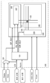
도 2에 본 발명의 일 형태에 따른 액정 표시 장치(100)의 블록도를 도시하였다. 액정 표시 장치(100)는 표시 제어 신호 생성 회로(101)와, 선택 회로(102)와, 표시 패널(103)을 갖는다.2 is a block diagram of the liquid
표시 패널(103)은 게이트 라인 구동 회로(104), 소스 라인 구동 회로(105), 및 화소부(106)를 갖는다. 화소부(106)는 복수의 화소(108)를 가지며, 화소(108)에 적어도 한 쌍의 전극을 갖는 액정 소자가 제공되어 있다. 게이트 라인 구동 회로(104)로부터 게이트 라인(109)에 공급되는 주사선 신호에 의해, 소스 라인(110)에 공급되는 비디오 신호의 화소(108)에 대한 기록이 제어된다. 또한, 소스 라인 구동 회로(105)는 디지털/아날로그 변환 회로(107)를 갖는 것이 바람직하다. 또한, 본 명세서 등에 있어서, 구동 회로라고 기재하는 경우에는 게이트 라인 구동 회로(104)와 소스 라인 구동 회로(105)를 포함하며, 더구나 표시 제어 신호 생성 회로(101), 선택 회로(102) 등도 포함하는 경우가 있다.The
표시 패널(103)에는 고전원 전위 VDD 및 저전원 전위 VSS를 기초로 하는 전원 전압, 공통 전위 Vcom이 공급된다.The
표시 제어 신호 생성 회로(101)는 외부로부터 입력되는 동기 신호에 기초하여 게이트 라인 구동 회로(104) 및 소스 라인 구동 회로(105)를 동작시키기 위한 신호를 출력하는 회로이다.The display control
동기 신호의 일례로서는 수평 동기 신호(Hsync.), 수직 동기 신호(Vsync.), 기준 클럭 신호(CLK)가 있다.Examples of the synchronization signal include a horizontal synchronization signal Hsync., A vertical synchronization signal Vsync., And a reference clock signal CLK.
게이트 라인 구동 회로(104)를 동작시키기 위한 신호로서는 게이트 라인 측 스타트 펄스 GSP, 게이트 라인 측 클럭 신호 GCLK 등이 있다. 또한, 게이트 라인 측 클럭 신호 GCLK는 위상이 시프트됨으로써 복수의 게이트 라인 측 클럭 신호가 된 것을 포함한다.Signals for operating the gate
소스 라인 구동 회로(105)를 동작시키기 위한 신호로서는 소스 라인 측 스타트 펄스 SSP, 소스 라인 측 클럭 신호 SCLK 등이 있다. 또한, 소스 라인 측 클럭 신호 SCLK는 위상이 시프트됨으로써 복수의 소스 라인 측 클럭 신호가 된 것을 포함한다.Signals for operating the source
또한, 소스 라인 구동 회로(105)가 갖는 디지털/아날로그 변환 회로(107)는 외부로부터 입력되는 데이터 신호 Data, 및 표시 제어 신호 생성 회로(101)로부터 입력되는 극성 반전 신호 POL이 공급된다. 디지털/아날로그 변환 회로(107)는 데이터 신호 Data를 극성 반전 신호 POL에 기초하여 아날로그 값의 비디오 신호로 변환한다. 이 데이터 신호를 아날로그 값의 비디오 신호로 변환할 때는 래더(ladder) 저항과 스위치를 조합한 회로로 수행하면 좋고, 동시에 감마 보정 등을 수행하는 구성으로 하면 좋다.The digital /
또한, 소스 라인 구동 회로(105)가 갖는 디지털/아날로그 변환 회로(107)는 입력되는 극성 반전 신호 POL에 따라, 화소에 출력하는 비디오 신호의 극성을 전환시킬 수 있는 회로이면 좋고, 다른 회로로 할 수도 있다. 예를 들어, 극성 반전 신호 POL에 따라, 화소에 출력하는 비디오 신호의 극성을 전환시키는 반전 증폭기(inverting amplifier)를 사용하여도 좋다.The digital /
외부로부터 입력되는 데이터 신호 Data는 디지털 데이터이다. 데이터 신호 Data가 아날로그 데이터인 경우에는 디지털 데이터로 변환한다.The data signal Data input from the outside is digital data. If the data signal Data is analog data, it is converted into digital data.
극성 반전 신호 POL은 데이터 신호 Data를 아날로그 신호인 비디오 신호(Vdata라고도 함)로 변환할 때, 상기 비디오 신호를 공통 전위에 대해 높은 전위(양의 극성) 및 낮은 전위(음의 극성) 중 어느 하나로 전환하는 신호이다.When the polarity inversion signal POL converts the data signal Data into a video signal (also called Vdata) which is an analog signal, the video signal is converted into one of a high potential (positive polarity) and a low potential (negative polarity) with respect to a common potential. It is a signal to switch.
비디오 신호 Vdata는 데이터 신호 Data에 기초한 전압이다. 비디오 신호 Vdata는 소스 라인(110)을 통하여 각 화소(108)의 액정 소자의 전극 중 하나에 인가되는 전압이다. 액정 소자에 대한 비디오 신호의 인가는 화소(108)에 대한 비디오 신호의 기록이라고도 한다. 극성이 상이한 비디오 신호 Vdata이어도 비디오 신호의 전위와 공통 전위의 차이의 절대값이 같으면, 액정 표시 장치에 입력되는 데이터 신호 Data는 같은 값이 된다. 또한, 비디오 신호는 비디오 신호의 전위가 공통 전위보다 높은 경우에는 액정 소자에 양의 극성의 전압이 인가된다. 한편, 비디오 신호의 전위가 공통 전위보다 낮은 경우에는 액정 소자에 음의 극성의 전압이 인가된다.The video signal Vdata is a voltage based on the data signal Data. The video signal Vdata is a voltage applied to one of the electrodes of the liquid crystal element of each
또한, 화소에 기록되는 비디오 신호는 기록되는 비디오 신호의 전압 레벨로부터, 더 보정된 전압 레벨로 변경함으로써, 액정 소자의 응답을 빠르게 할 수 있다. 예를 들어, 비디오 신호의 전압 레벨을 더 큰 전압 레벨의 비디오 신호로 보정함으로써, 액정 소자의 응답 시간을 짧게 하여, 화상 표시를 신속하게 수행할 수 있다. 이와 같은 보정 신호를 인가하는 구동 방법은 오버드라이브 구동이라고도 불린다.In addition, the video signal recorded in the pixel can be changed from the voltage level of the video signal to be recorded to a more corrected voltage level, thereby speeding up the response of the liquid crystal element. For example, by correcting the voltage level of the video signal to a video signal of a larger voltage level, the response time of the liquid crystal element can be shortened, and image display can be performed quickly. The driving method for applying such a correction signal is also called overdrive driving.
또한, 표시 제어 신호 생성 회로(101)에 있어서, 출력되는 극성 반전 신호 POL의 신호의 반전을 m프레임 기간마다 수행하기 위해서는, 예를 들어 동기 신호인 수직 동기 신호(Vsync.)의 주기를 m주기 카운트하여 극성 반전 신호 POL의 신호를 반전하는 구성으로 하면 좋다. 구체적으로는 수직 동기 신호의 주기를 카운트하여 얻어지는 카운트 값을 표시 제어 신호 생성 회로(101)에 출력하는 카운터 회로를 제공하면 좋다. 카운터 회로가 수직 동기 신호의 카운트 값을 m주기로 리셋하여, 표시 제어 신호 생성 회로(101)가 상기 리셋에 따라 극성 반전 신호 POL의 전위의 H 레벨과 L 레벨을 전환하는 구성으로 하면 좋다.In addition, in the display control
또한, 표시 제어 신호 생성 회로(101)는 액정 표시 장치(100)를 비표시 상태로 할 때는 외부로부터 입력되는 정지 신호(STP)에 따라 극성 반전 신호 RPOL을 출력한다. 여기서, 정지 신호 STP가 표시 제어 신호 생성 회로(101)에 입력되면, 극성 반전 신호 POL의 출력이 정지되고, 이 대신에 극성 반전 신호 RPOL이 출력된다.When the liquid
또한, 선택 회로(102)는 정지 신호 STP에 따라 데이터 신호 Data 또는 리셋 데이터 신호 Rdata를 선택하여 디지털/아날로그 변환 회로(107)에 출력한다. 정지 신호 STP가 입력되지 않을 때는 선택 회로(102)는 데이터 신호 Data를 출력하고, 정지 신호 STP가 입력되면 선택 회로(102)는 리셋 데이터 신호 Rdata를 출력한다. 여기서, 리셋 데이터 신호 Rdata는 데이터 신호 Data와 마찬가지로 디지털 데이터이다.In addition, the
디지털/아날로그 변환 회로(107)에 출력된 리셋 데이터 신호 Rdata는 극성 반전 신호 RPOL에 따라 아날로그 값의 리셋 신호(Vres라고도 부름)로 변환된다. 즉 극성 반전 신호 RPOL은 리셋 데이터 신호 Rdata를 아날로그 신호인 리셋 신호 Vres로 변환할 때, 상기 리셋 신호를 공통 전위보다 높은 전위(양의 극성) 및 낮은 전위(음의 극성) 중 어느 하나로 전환하는 신호이다.The reset data signal Rdata output to the digital /
화상을 표시할 때는 수직 동기 신호(Vsync.)에 따라 표시 제어 신호 생성 회로(101)로부터 극성 반전 신호 POL이 출력되고, 선택 회로(102)로부터 출력된 데이터 신호 Data는 디지털/아날로그 변환 회로(107)에서 극성 반전 신호 POL에 따라 비디오 신호 Vdata로 변화된다. 한편, 화상을 비표시 상태로 할 때는 정지 신호 STP에 따라 표시 제어 신호 생성 회로(101)로부터 극성 반전 신호 RPOL이 출력되고, 선택 회로(102)로부터 출력된 리셋 데이터 신호 Rdata는 디지털/아날로그 변환 회로(107)에서 극성 반전 신호 RPOL에 따라 리셋 신호 Vres로 변화된다.When displaying an image, the polarity inversion signal POL is output from the display control
도 3의 (A)는 액정 표시 장치(100)의 화상을 표시할 때, 표시 제어 신호 생성 회로(101), 선택 회로(102), 및 표시 패널(103)에 입출력되는 신호를 모식적으로 도시한 타이밍 차트이다.FIG. 3A schematically illustrates signals input and output to the display control
도 3의 (A)의 타이밍 차트는 수직 동기 신호(Vsync.), 데이터 신호(data), 극성 반전 신호 POL의 파형을 모식적으로 도시한 것이다. 또한, 도 3의 (A)에 도시한 타이밍 차트에서는 가로축은 시간을 나타내고, 세로축은 화소의 액정 소자에 인가하는 비디오 신호 Vdata의 전압 레벨을 나타낸다.The timing chart of FIG. 3A schematically shows the waveforms of the vertical synchronization signal Vsync., The data signal data, and the polarity inversion signal POL. In addition, in the timing chart shown in Fig. 3A, the horizontal axis represents time, and the vertical axis represents the voltage level of the video signal Vdata applied to the liquid crystal element of the pixel.
도 3의 (A)에 도시한 타이밍 차트에서는 수직 동기 신호의 H 레벨의 주기에 동기하여, 데이터 신호가 첫 번째 프레임 내지 m 번째(m은 2 이상의 자연수) 프레임에서 연속하여 공급된다. 극성 반전 신호 POL은 수직 동기 신호의 H 레벨을 카운트하여 m번마다 신호를 반전한다. 그래서, 극성 반전 신호 POL을 m프레임마다 반전한 신호를 할 수 있다.In the timing chart shown in Fig. 3A, in synchronization with the period of the H level of the vertical synchronization signal, the data signal is supplied continuously in the first to mth frames (m is a natural number of two or more). The polarity inversion signal POL inverts the signal every m times by counting the H level of the vertical synchronization signal. Thus, a signal obtained by inverting the polarity inversion signal POL every m frames can be performed.
극성 반전 신호 POL의 반전에 따라 양의 극성 또는 음의 극성으로 반전되는 비디오 신호는 공통 전위에 대한 전압 레벨로서 각 화소에 기록된다. 도 3의 (A)에 도시한 바와 같이, 본 실시형태의 구성에서는 m프레임 기간 연속적으로 같은 극성의 반전 상태를 유지하여 동작시킬 수 있다.The video signal inverted to the positive polarity or the negative polarity in accordance with the inversion of the polarity inversion signal POL is written to each pixel as the voltage level with respect to the common potential. As shown in Fig. 3A, in the configuration of the present embodiment, the operation can be performed while maintaining the inverted state of the same polarity continuously for m frame periods.
일반적으로 표시 소자에 액정 소자를 사용하는 표시 장치에서는 게이트 라인 반전 구동, 소스 라인 반전 구동, 프레임 반전 구동, 도트 반전 구동이라는, 1프레임 기간마다 양 또는 음의 극성을 교대로 표시 소자에 공급하는 반전 구동을 수행한다. 그러나, 액정 소자에 인가하는 비디오 신호의 전압 레벨이 큰 경우에 반전 구동을 수행하면, 표시 소자에 인가하는 전압 레벨의 크기가 변하지 않아도 신호의 반전에 의해 비디오 신호의 변화량이 커져, 소비 전력이 커진다. 소비 전력의 증대는 구동 주파수가 큰 구동이 수행되는 경우에 특히 현저하게 된다.In general, in a display device using a liquid crystal element for a display element, an inversion in which positive or negative polarities are alternately supplied to the display element every one frame period, namely, gate line inversion driving, source line inversion driving, frame inversion driving, and dot inversion driving. Perform the drive. However, if inversion driving is performed when the voltage level of the video signal applied to the liquid crystal element is large, the amount of change in the video signal is increased due to the inversion of the signal even if the magnitude of the voltage level applied to the display element does not change, thereby increasing the power consumption. . The increase in power consumption becomes particularly remarkable when driving with a large driving frequency is performed.
한편, 도 3의 (A)에 도시한 예에서는 같은 극성의 비디오 신호를 m프레임 기간 이상 연속적으로 인가함으로써 기록할 수 있다. 그러므로, 1프레임 기간마다 반전 구동을 수행한 경우에 반전 구동에 따른 비디오 신호의 변화량이 커진다는 문제를 저감할 수 있어, 소비 전력을 절감할 수 있다.On the other hand, in the example shown in Fig. 3A, recording can be performed by applying video signals having the same polarity continuously for m frame periods or more. Therefore, when the inversion driving is performed every one frame period, the problem that the amount of change in the video signal due to the inversion driving is increased can be reduced, and power consumption can be reduced.
또한, 도 3의 (A)에 도시한 바와 같이, 본 실시형태에서 제시한 구성에서는 m프레임 기간마다 반전 구동한다. 그러므로, m 번째 프레임부터 (m+1) 번째 프레임간, 및 2m 번째 프레임부터 (2m+1) 번째 프레임간에서는 비디오 신호의 변화가 커진다. 한편, m 번째 프레임부터 (m+1) 번째 프레임, 및 2m 번째 프레임부터 (2m+1) 번째 프레임에서는 비디오 신호를 공통 전위 Vcom과 대략 같은 전위로 하는 블랭크 기간을 설정하는 구성으로 함으로써, 비디오 신호의 변화를 작게 할 수 있다. 이로써, 소비 전력을 더 저감할 수 있다.In addition, as shown in Fig. 3A, the configuration shown in the present embodiment is inverted for every m frame period. Therefore, the change in the video signal increases between the m-th frame to the (m + 1) th frame and between the 2m-th frame to the (2m + 1) th frame. On the other hand, the video signal is configured by setting a blank period in which the video signal is at the same potential as the common potential Vcom in the m-th frame from the (m + 1) th frame and from the 2m-th frame to the (2m + 1) th frame. The change of can be made small. Thereby, power consumption can be further reduced.
또한, 도 3의 (B)는 액정 표시 장치(100)의 화상을 비표시 상태로 할 때의 표시 제어 신호 생성 회로(101), 선택 회로(102), 및 표시 패널(103)에 입출력되는 신호를 모식적으로 도시한 타이밍 차트이다.3B is a signal input / output to the display control
도 3의 (B)에 도시한 타이밍 차트에 정지 신호(STP), 리셋 데이터 신호(Rdata), 극성 반전 신호 RPOL의 파형을 모식적으로 도시하였다. 또한, 도 3의 (B)에 도시한 타이밍 차트에서는 가로축은 시간을 나타내고, 세로축은 화소의 액정 소자에 인가하는 리셋 신호 Vres의 전압 레벨을 나타낸다.The waveform of the stop signal STP, the reset data signal Rdata, and the polarity inversion signal RPOL is schematically shown in the timing chart shown in FIG. 3B. In addition, in the timing chart shown in FIG. 3B, the horizontal axis represents time, and the vertical axis represents the voltage level of the reset signal Vres applied to the liquid crystal element of the pixel.
도 3의 (B)에 도시한 타이밍 차트에서는 정지 신호 STP의 H 레벨이 입력되면, 리셋 데이터 신호가 R1 번째 프레임 및 R2 번째 프레임에 입력된다. 여기서 R1 번째 프레임이란, 정지 신호 STP가 입력되고 나서 첫 번째 프레임을 뜻하고, R2 번째 프레임이란, 정지 신호 STP가 입력되고 나서 2 번째 프레임을 뜻한다. 극성 반전 신호 RPOL은 R1 번째 프레임과 R2 번째 프레임에서 반전되며, 도 3의 (B)에서는 극성 반전 신호 RPOL은 R1 번째 프레임에서 양의 극성이 되고 R2 번째 프레임에서 음의 극성이 된다.In the timing chart shown in FIG. 3B, when the H level of the stop signal STP is input, the reset data signal is input to the R1 th frame and the R2 th frame. The R1 th frame means the first frame after the stop signal STP is input, and the R2 th frame means the second frame after the stop signal STP is input. The polarity inversion signal RPOL is inverted in the R1 th frame and the R2 th frame. In FIG. 3B, the polarity inversion signal RPOL becomes a positive polarity in the R1 th frame and a negative polarity in the R2 th frame.
극성 반전 신호 RPOL에 따라 양의 극성 또는 음의 극성으로 반전되는 리셋 신호 Vres는 공통 전위 Vcom에 대한 전압 레벨로서 각 화소에 기록된다. 도 3의 (B)에서는 리셋 신호 Vres는 R1 번째 프레임에서 양의 극성이 되고 R2 번째 프레임에서 음의 극성이 된다. 이 때, 전압 레벨의 절대값은 최대한 크게, 예를 들어 비디오 신호의 전압 레벨의 절대값의 최대값과 같은 정도로 하는 것이 바람직하다. 또한, R1 번째 프레임의 리셋 신호 Vres의 극성은 정지 신호 STP가 입력되었을 때의 비디오 신호 Vdata의 극성을 반전시킨 극성으로 하는 것이 바람직하다. 이와 같이 리셋 신호 Vres를 모든 화소에 입력한 후, 고전원 전위 VDD의 공급을 차단하면 좋다.The reset signal Vres inverted to the positive polarity or the negative polarity in accordance with the polarity inversion signal RPOL is written to each pixel as the voltage level for the common potential Vcom. In FIG. 3B, the reset signal Vres becomes a positive polarity in the R1 th frame and a negative polarity in the R2 th frame. At this time, it is preferable that the absolute value of the voltage level is as large as possible, for example, as much as the maximum value of the absolute value of the voltage level of the video signal. In addition, it is preferable that the polarity of the reset signal Vres of the R1 < th > frame is a polarity inverting the polarity of the video signal Vdata when the stop signal STP is input. In this way, after the reset signal Vres is input to all the pixels, the supply of the high power supply potential VDD may be cut off.
이와 같이 리셋 신호 Vres를 입력함으로써, 상술한 바와 같이 m프레임 기간 이상 연속적으로 같은 극성의 비디오 신호를 기록하여도 액정의 열화를 억제할 수 있다. 따라서, 동영상을 표시하는 경우에도 소비 전력의 저감이 도모된 데다가 액정의 열화를 억제할 수 있는 액정 표시 장치를 제공할 수 있다.By inputting the reset signal Vres in this manner, deterioration of the liquid crystal can be suppressed even when the video signal of the same polarity is recorded continuously for m frame periods or more as described above. Therefore, even when a moving picture is displayed, the power consumption can be reduced, and the liquid crystal display device which can suppress deterioration of a liquid crystal can be provided.
또한, 도 3의 (B)에서는 리셋 신호로서 R1 번째 프레임과 R2 번째 프레임의 2프레임에 양의 극성과 음의 극성의 전위를 각각 인가하지만, 이것에 한정되지 않으며, 3프레임 이상 전위의 극성을 반전시키면서 리셋 신호를 입력시키는 구성으로 하여도 좋다. 또한, 정지 신호 STP가 입력되었을 때의 비디오 신호 Vdata의 전위의 극성을 반전시킨 극성을 갖는 전위의 리셋 신호를 1프레임만 입력시키는 구성으로 할 수도 있다.In FIG. 3B, the potentials of the positive polarity and the negative polarity are respectively applied to the two frames of the R1 and R2 frames as reset signals, but the present invention is not limited thereto. The reset signal may be input while being inverted. It is also possible to have a configuration in which only one frame of the reset signal having the polarity having the polarity inverted the polarity of the potential of the video signal Vdata when the stop signal STP is input is input.
또한, 도 3의 (B)에서는 R1 번째 프레임의 길이, R2 번째 프레임의 길이는 도 3의 (A)에 도시한 1프레임 기간과 같은 정도이지만, 본 실시형태에 제시되는 액정 표시 장치는 이것에 한정되지 않으며, R1 번째 프레임, R2 번째 프레임, 또는 R3 번째 프레임 이후의 프레임의 길이를 1프레임 기간 이상의 길이로 하여도 좋다.In addition, in FIG. 3B, the length of the R1 th frame and the length of the R2 th frame are about the same as the one frame period shown in FIG. The length of the frame after the R1 th frame, the R2 th frame, or the R3 th frame may be equal to or longer than one frame period.
또한, 이와 같이 리셋 신호 Vres로서 적어도 한 번 이상 극성을 반전시키면서 전위를 입력한 후, 리셋 신호 Vres의 전위를 공통 전위 Vcom과 대략 같은 전위로 하는 것이 바람직하다. 예를 들어, 도 3의 (B)에 있어서, R2 번째 프레임 다음에 리셋 신호의 전압 레벨이 공통 전위 Vcom이 되는 R3 번째 프레임을 제공하는 구성으로 하면 좋다. 또한, 이와 같이 하여 액정 소자의 전극 간의 전위차를 대략 0V로 한 후, 화소에 제공된 액정 소자와 전기적으로 접속된 트랜지스터를 오프 상태로 하는 것이 바람직하다.In this way, it is preferable that the potential of the reset signal Vres is approximately the same as the common potential Vcom after inputting the potential while reversing the polarity at least once as the reset signal Vres. For example, in Fig. 3B, the R3 th frame may be provided after the R2 th frame so that the voltage level of the reset signal becomes the common potential Vcom. In this way, it is preferable that the potential difference between the electrodes of the liquid crystal element is approximately 0 V, and then the transistor electrically connected to the liquid crystal element provided in the pixel is turned off.
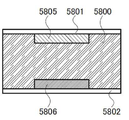
다음에, 도 2에 도시한 표시 패널(103)의 구성에 대해서, 구체적인 구성예를 제시하며, 본 실시형태의 효과에 대해서 자세히 설명한다.Next, a specific structural example is shown about the structure of the
도 4는 도 2에 도시한 표시 패널(103)이 갖는 게이트 라인 구동 회로(104), 소스 라인 구동 회로(105), 및 화소부(106)의 구성을 구체적으로 도시한 것이다.4 illustrates the structure of the gate
게이트 라인 구동 회로(104)는 시프트 레지스터 회로(201)를 갖는다. 소스 라인 구동 회로(105)는 시프트 레지스터 회로(202), 디지털/아날로그 변환 회로(107), 및 아날로그 스위치(203)를 갖는다.The gate
도 4에서는 일례로서 화소부(106)가 3행 3열의 화소(108)를 갖는 구성을 도시하였다. 화소(108)는 각각 트랜지스터(204), 용량 소자(205), 및 액정 소자(206)를 갖는다. 트랜지스터(204)는 게이트가 게이트 라인(109)에 접속되고, 소스 및 드레인 중 하나가 소스 라인(110)에 접속된다.In FIG. 4, as an example, a configuration in which the
트랜지스터(204)로서는 오프 상태에서의 전류(오프 전류)가 낮은 트랜지스터를 사용하는 것이 바람직하며, 예를 들어 산화물 반도체를 사용한 트랜지스터를 사용하는 것이 바람직하다. 이와 같은 트랜지스터를 트랜지스터(204)로서 사용함으로써, 용량 소자(205) 및 액정 소자(206)로부터 트랜지스터(204)를 통하여 전하가 누설되기 어려워지기 때문에, 액정 소자(206)에 인가하는 전압을 장시간 유지할 수 있다. 이로써, 액정 표시 장치(100)의 표시 화상의 유지 특성을 높일 수 있다.As the
한편, 이와 같이 트랜지스터(204)로서 오프 전류가 낮은 트랜지스터를 사용하면, 액정 표시 장치(100)의 전원을 오프 상태로 한 후에도, 트랜지스터(204)와 접속되는 액정 소자(206)의 전압이 유지되고, 극성이 유지된 전계가 액정에 장시간 인가되어 액정이 열화될 우려가 있다. 한편, 상술한 바와 같이 리셋 신호를 입력할 때, 적어도 한 번 이상 극성을 반전시키면서 전위를 입력한 후, 리셋 신호 Vres의 전위를 공통 전위 Vcom과 대략 같은 전위로 하여 트랜지스터(204)를 오프 상태로 함으로써, 극성이 유지된 전계가 액정에 장시간 인가되는 것을 억제할 수 있다.On the other hand, when a transistor having a low off current is used as the
또한, 상술한 바와 같이 액정 표시 장치(100)의 전원이 오프 상태일 때, 타이머로 설정한 시간에 액정 표시 장치(100)를 기동시켜 상기 리셋 신호를 입력하는 구성으로 하는 것이 바람직하다. 이로써, 액정 표시 장치(100)의 전원을 오프 상태로 하였을 때, 액정 소자(206)의 전압이 유지되어 있어도, 타이머로 설정한 시각에 액정의 상태를 전계가 인가되지 않는 상태로 할 수 있다.As described above, when the power supply of the liquid
도 4에 있어서, 게이트 라인 구동 회로(104)가 갖는 시프트 레지스터 회로(201)는 게이트 라인 측 스타트 펄스 GSP, 게이트 라인 측 클럭 신호 GCLK가 입력된다. 시프트 레지스터 회로(201)는 첫 번째 행 내지 3 번째 행에 있는 게이트 라인(109)에 대해 선택 신호 Gout1 내지 선택 신호 Gout3을 사용하여 순차적으로 H 레벨의 신호를 출력하여, 트랜지스터(204)의 도통 상태를 제어할 수 있다.In FIG. 4, the gate line side start pulse GSP and the gate line side clock signal GCLK are input to the
도 4에 있어서, 소스 라인 구동 회로(105)가 갖는 디지털/아날로그 변환 회로(107)는 화상을 표시할 때는 데이터 신호 Data, 및 극성 반전 신호 POL에 따라 생성되는 비디오 신호 Vdata를 출력한다. 또한, 화상을 비표시 상태로 할 때는 리셋 데이터 신호 Rdata, 및 극성 반전 신호 RPOL에 따라 생성되는 리셋 신호 Vres를 출력한다. 비디오 신호 Vdata 및 리셋 신호 Vres는 아날로그 스위치(203)가 도통 상태가 됨으로써, 소스 라인(110)을 통하여 화소(108)의 용량 소자(205) 및 액정 소자(206)에 기록된다.In Fig. 4, the digital /
도 4에 있어서, 소스 라인 구동 회로(105)가 갖는 시프트 레지스터 회로(202)는 소스 라인 측 스타트 펄스 SSP, 소스 라인 측 클럭 신호 SCLK가 입력된다. 시프트 레지스터 회로(202)는 첫 번째 열 내지 3 번째 열에 있는 아날로그 스위치(203)에 대해 선택 신호 Sout1 내지 선택 신호 Sout3을 사용하여 순차적으로 H 레벨의 신호를 출력하여, 아날로그 스위치(203)의 도통 상태를 제어할 수 있다.In Fig. 4, the
다음에, 도 5의 (A)에 도시한 화소부의 모식도, 및 도 5의 (B)에 도시한, 데이터 신호에 기초하는 양 또는 음의 극성을 갖는 비디오 신호의 도면을 사용하여, 복수의 프레임 기간에 걸친 본 발명의 구동 방법의 구체적인 동작의 일례에 대해서 설명한다.Next, using a schematic diagram of the pixel portion shown in FIG. 5A and a diagram of a video signal having a positive or negative polarity based on the data signal shown in FIG. 5B, a plurality of frames An example of the specific operation of the driving method of the present invention over the period will be described.
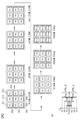
도 5의 (A)에 도시한 도면은 화상을 표시할 때의 첫 번째 프레임, 2 번째 프레임, m 번째 프레임, 및 (m+1) 번째 프레임, 화상을 비표시로 할 때의 R1 번째 프레임, R2 번째 프레임, 및 R3 번째 프레임에, 3행 3열의 화소부에 입력되는 데이터 신호의 모식도이다. 여기서, R1 번째 프레임이란, 정지 신호 STP가 입력되고 나서 첫 번째 프레임을 뜻하고, R2 번째 프레임이란, 2 번째 프레임을 뜻하고, R3 번째 프레임이란, 3 번째 프레임을 뜻한다.5A shows a first frame, a second frame, an mth frame, and an (m + 1) th frame when the image is displayed, an R1th frame when the image is not displayed, It is a schematic diagram of the data signal input to the pixel part of 3rd row and 3rd column to the R2nd frame and the R3th frame. Here, the R1 th frame means the first frame after the stop signal STP is input, the R2 th frame means the second frame, and the R3 th frame means the third frame.
도 5의 (A)에 도시한 첫 번째 프레임은 1행 1열째의 화소(211), 2행 1열째의 화소(221), 및 3행 1열째의 화소(231)에는 데이터 신호로서 'VA'를 입력하고, 1행 2열째의 화소(212), 2행 2열째의 화소(222), 및 3행 2열째의 화소(232)에는 데이터 신호로서 'VB'를 입력하고, 1행 3열째의 화소(213), 2행 3열째의 화소(223), 및 3행 3열째의 화소(233)에는 데이터 신호로서 'VC'를 입력하는 예이다.In the first frame shown in FIG. 5A, the
또한, 도 5의 (A)에 도시한 데이터 신호 'VA', 'VB', 및 'VC'를 비디오 신호의 전압 레벨의 크기로 표현하려면, |VA|, |VB|, |VC|로 표현할 수 있다. 또한, 설명을 위해 |VA|, |VB|, |VC|의 대소 관계를 일례로서 나타내면, |VC|<|VB|<|VA|가 된다. 극성 반전 신호 POL이 H 레벨(POL_H)인 경우에는, 도 5의 (B)에 도시한 바와 같이 비디오 신호는 'VA', 'VB', 및 'VC'로 표기할 수 있고, '양의 극성의 비디오 신호를 기록한다'라고 설명할 수 있다. 또한, 극성 반전 신호 POL이 L 레벨(POL_L)인 경우에, 도 5의 (B)에 도시한 바와 같이 비디오 신호는 '-VA', '-VB', 및 '-VC'로 표기할 수 있고, '음의 극성의 비디오 신호를 기록한다'라고 설명할 수 있다. 또한, 도 5의 (B)에 도시한 바와 같이, 'VA', 'VB', 및 'VC'와, '-VA', '-VB', 및 '-VC'의 비디오 신호는 공통 전위 Vcom을 사이에 두고 대칭이 되고, 크기가 같은 신호이다.In addition, to express the data signals 'V A ', 'V B ', and 'V C ' shown in FIG. 5A by the magnitude of the voltage level of the video signal, | V A |, | V B |, It can be expressed as | V C |. Also, for purposes of explanation | V A |, | V B |, | represents as an example the case of the relationship, | | V C V C | is a | <| V B | <| V A. When the polarity inversion signal POL is at the H level POL_H, as shown in FIG. 5B, the video signal may be expressed as' V A ',' V B ', and' V C ', and' Record a video signal of positive polarity '. In addition, when the polarity inversion signal POL is at the L level (POL_L), as shown in FIG. 5B, the video signal is represented by '-V A ', '-V B ', and '-V C '. This can be described as 'recording a video signal of negative polarity'. In addition, as shown in FIG. 5B, of 'V A ', 'V B ', and 'V C ', and of '-V A ', '-V B ', and '-V C ' The video signal is a symmetrical signal with the common potential Vcom in between.
또한, 도 5의 (A)에 있어서, 2 번째 프레임에서는 화소(211), 화소(221), 및 화소(231)에 'VB'를 입력하고, 화소(212), 화소(222), 및 화소(232)에 'VC'를 입력하고, 화소(213), 화소(223), 및 화소(233)에 'VA'를 데이터 신호로서 입력한다.In FIG. 5A, 'V B ' is input to the
또한, 도 5의 (A)에 있어서, m 번째 프레임에서는 화소(211), 화소(221), 및 화소(231)에 'VC'를 입력하고, 화소(212), 화소(222), 및 화소(232)에 'VA'를 입력하고, 화소(213), 화소(223), 및 화소(233)에 'VB'를 데이터 신호로서 입력한다.In FIG. 5A, 'V C ' is input to the
또한, 도 5의 (A)에 있어서, (m+1) 번째 프레임에서는 화소(211), 화소(221), 및 화소(231)에 'VB'를 입력하고, 화소(212), 화소(222), 및 화소(232)에 'VC'를 입력하고, 화소(213), 화소(223), 및 화소(233)에 'VA'를 데이터 신호로서 입력한다.In FIG. 5A, 'V B ' is inputted to the
또한, 도 5의 (A)에 있어서, R1 번째 프레임에서는 모든 화소에 'VA'를 데이터 신호로서 입력하고, R2 번째 프레임에서도 마찬가지로 모든 화소에 'VA'를 데이터 신호로서 입력한다. 또한, 도 5의 (A)에 있어서, R3 번째 프레임에서는 모든 화소에 공통 전위 Vcom에 대응하는 'Vcom'를 데이터 신호로서 입력한다.Further, in (A) of Figure 5, the R1-th frame and inputs the 'V A' to all of the pixels a 'V A' and type as the data signal, as R2 in the second frame to all of the pixels as the data signal. In Fig. 5A, 'V com ' corresponding to the common potential V com is input as a data signal to all the pixels in the R3 th frame.
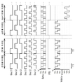
도 6은 도 5의 (A)에 도시한, 화상을 표시할 때의 화소부로의 데이터 신호의 입력에 기초하여 도시한 타이밍 차트이다. 도 6에 도시한 타이밍 차트에서는 첫 번째 프레임, 2 번째 프레임, m 번째 프레임, 및 (m+1) 번째 프레임에서의 선택 신호 Gout1 내지 선택 신호 Gout3, 선택 신호 Sout1 내지 선택 신호 Sout3, 데이터 신호 Data, 극성 반전 신호 POL, 및 비디오 신호 Vdata를 도시하였다. 또한, 도 6에 도시한 타이밍 차트에서는 점순차 구동으로 한 경우에 대해서 설명하지만, 선순차 구동으로 하는 구성이어도 좋다.FIG. 6 is a timing chart shown based on the input of a data signal to the pixel portion at the time of displaying an image shown in FIG. In the timing chart shown in Fig. 6, the selection signals Gout1 through selection signal Gout3, the selection signals Sout1 through selection signal Sout3, the data signal Data, in the first frame, the second frame, the mth frame, and the (m + 1) th frame, The polarity inversion signal POL and the video signal Vdata are shown. In addition, although the timing chart shown in FIG. 6 demonstrates the case where it uses the point sequential drive, the structure made into the line sequential drive may be sufficient.
도 6에 도시한 타이밍 차트에서는 도 3의 (A)에서 설명한 바와 같이, 극성 반전 신호 POL의 신호를 m프레임 기간마다 반전시키는 구성으로 할 수 있다. 따라서, 본 실시형태에서의 비디오 신호 Vdata를 m프레임 기간 연속적으로, 같은 극성의 비디오 신호로 하여 동작시킬 수 있다. 그러므로, 1프레임 기간마다 반전 구동을 수행한 경우에, 반전 구동에 따른 비디오 신호의 변화량이 커진다는 문제를 저감할 수 있어, 소비 전력을 절감할 수 있다.In the timing chart shown in FIG. 6, as described with reference to FIG. 3A, the polarity inversion signal POL can be inverted every m frame period. Therefore, it is possible to operate the video signal Vdata according to the present embodiment as a video signal having the same polarity continuously for m frame periods. Therefore, when inversion driving is performed every one frame period, the problem that the amount of change of the video signal due to the inversion driving is increased can be reduced, and power consumption can be reduced.
다음에 도 7에서는 도 6에 도시한 타이밍 차트에서 화소부에서의 첫 번째 열의 비디오 신호의 변화를 발췌해서 설명한다.Next, in FIG. 7, the variation of the video signal of the first column in the pixel portion in the timing chart shown in FIG. 6 will be described.
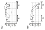
도 7의 (A)에 도시한 도면은 도 6에 도시한 기간 T1 및 기간 T2에서의 비디오 신호의 변화를 발췌해서 도시한 모식도이다. 또한, 도 7의 (B)에 도시한 도면은 도 6에 도시한 타이밍 차트에 대해 1프레임마다 극성 반전 신호 POL을 반전시키는 구성으로 한 경우의, 도 6의 기간 T1 및 기간 T2에 대응하는 기간 T1R 및 기간 T2R에서의 비디오 신호의 변화를 발췌해서 도시한 모식도이다. 즉, 도 7의 (B)에서는 기간 T1R 및 기간 T2R에서 비디오 신호의 극성이 반전되어 있다.FIG. 7A is a schematic diagram showing an excerpt of the change in the video signal in the period T1 and the period T2 shown in FIG. 6. 7B is a period corresponding to the period T1 and the period T2 of FIG. 6 in the case where the polarity inversion signal POL is inverted for each frame with respect to the timing chart shown in FIG. 6. It is a schematic diagram which extracts and shows the change of the video signal in T1R and the period T2R. That is, in FIG. 7B, the polarities of the video signals are reversed in the periods T1R and T2R.
도 7의 (A)에 도시한 기간 T1은 첫 번째 프레임의 첫 번째 행의 각 열에서의 비디오 신호를 나타낸다. 도 7의 (A)에 도시한 기간 T2는 2 번째 프레임의 첫 번째 행의 각 열에서의 비디오 신호를 나타낸다. 도 7의 (B)에 도시한 기간 T1R는 첫 번째 프레임의 첫 번째 행의 각 열에서의 비디오 신호를 나타낸다. 도 7의 (B)에 도시한 기간 T2R는 2 번째 프레임의 첫 번째 행의 각 열에서의 비디오 신호를 나타낸다. 또한, 도 7의 (A) 및 (B)에서는 기간 T1과 기간 T2와, 기간 T1R과 기간 T2R에 있어서, 같은 열에서의 비디오 신호에 착안하여, 이들의 변화에 대해서 화살표로 가리켰다.A period T1 shown in FIG. 7A represents a video signal in each column of the first row of the first frame. A period T2 shown in FIG. 7A represents a video signal in each column of the first row of the second frame. A period T1R shown in FIG. 7B represents a video signal in each column of the first row of the first frame. A period T2R shown in FIG. 7B represents a video signal in each column of the first row of the second frame. In Figs. 7A and 7B, in the period T1, the period T2, and the period T1R and the period T2R, video signals in the same column are taken into consideration, and these changes are indicated by arrows.
도 7의 (A)에 있어서, 1행의 각 열의 첫 번째 프레임과 2번째 프레임 사이의 비디오 신호의 차이를 열거하면, 첫 번째 열에서는 |VA-VB|이고, 2 번째 열에서는 |VB-VC|이고, 3 번째 열에서는 |VC-VA|이다. 또한, 도 7의 (B)에 있어서, 1행의 각 열의 첫 번째 프레임과 2번째 프레임 사이의 비디오 신호의 차이를 열거하면, 첫 번째 열에서는 |VA+VB|이고, 2 번째 열에서는 |VB+VC|이고, 3 번째 열에서는 |VC+VA|이다.In Fig. 7A, when the difference of the video signal between the first frame and the second frame of each column of one row is enumerated, it is | V A -V B | in the first column and | V in the second column. B -V C |, and in the third column, | V C -V A | In Fig. 7B, when the difference in the video signal between the first frame and the second frame of each column of one row is enumerated, it is | V A + V B | in the first column, and in the second column. | V B + V C |, and in the third column, | V C + V A |.
도 7의 (A)와 (B)에 있어서, 같은 열에서의 비디오 신호에 착안하면, 전압의 변화가 큰 것은 도 7의 (B)에 도시한 1프레임마다 극성 반전 신호 POL을 반전시키는 프레임 반전 구동으로 한 경우이다. 한편, 도 7의 (A)에 도시한 극성 반전 신호 POL의 신호의 반전을 m프레임 기간마다 수행하는 구성으로 한 경우에는 같은 열에서의 비디오 신호의 변화가 작다. 따라서, 도 7의 (A)의 경우에는, 화소에 기록하는 비디오 신호의 충방전에 필요한 소비 전력을 작게 할 수 있다.In Figs. 7A and 7B, focusing on the video signals in the same column, the larger the voltage change, the more inverted the frame inverting the polarity inversion signal POL is for each frame shown in Fig. 7B. In the case of driving. On the other hand, when the configuration of the inversion of the signal of the polarity inversion signal POL shown in FIG. 7A is performed every m frame periods, the change of the video signal in the same column is small. Therefore, in the case of Fig. 7A, the power consumption required for charging and discharging the video signal recorded in the pixel can be reduced.
따라서, 동영상을 표시하는 경우에도 소비 전력의 저감이 도모된 액정 표시 장치를 제공할 수 있다.Therefore, even when displaying a moving picture, the liquid crystal display device with which the power consumption was reduced can be provided.
도 8은 도 5의 (A)에 도시한 화상을 비표시 상태로 할 때의 화소부에 대한 데이터 신호의 입력에 기초하여 도시한 타이밍 차트이다. 도 8에 도시한 타이밍 차트에서는 R1 번째 프레임, R2 번째 프레임, 및 R3 번째 프레임에서의 선택 신호 Gout1 내지 선택 신호 Gout3, 선택 신호 Sout1 내지 선택 신호 Sout3, 리셋 데이터 신호 Rdata, 극성 반전 신호 RPOL, 및 리셋 신호 Vres를 도시하였다. 또한, 도 8에 도시한 타이밍 차트에서는 점순차 구동으로 한 경우에 대해서 설명하지만, 선순차 구동으로 하는 구성이어도 좋다.FIG. 8 is a timing chart shown based on input of a data signal to a pixel portion when the image shown in FIG. 5A is made non-displayed. In the timing chart shown in Fig. 8, the selection signals Gout1 to selection signal Gout3, the selection signals Sout1 to selection signal Sout3, the reset data signal Rdata, the polarity inversion signal RPOL, and the reset in the R1th frame, the R2th frame, and the R3th frame are shown. The signal Vres is shown. In addition, although the timing chart shown in FIG. 8 demonstrates the case where it uses the point sequential drive, the structure made into the linear sequential drive may be sufficient.
도 8에 도시한 타이밍 차트에서는 도 3의 (B)에서 설명한 바와 같이, 극성 반전 신호 RPOL의 전위를 R1 번째 프레임과 R2 번째 프레임 간에서 반전시킨다. 이로써, R1 번째 프레임에서는 리셋 신호 Vres로서 전위 VA가 입력되고, R2 번째 프레임에서는 리셋 신호 Vres로서 전위 -VA가 입력된다. 이와 같이 리셋 신호 Vres를 입력함으로써, 도 6에 도시한 바와 같이 같은 극성의 비디오 신호를 m프레임 기간 이상 연속적으로 기록하여도, 액정의 열화를 억제할 수 있다. 또한, 리셋 신호 Vres의 전위를, 이와 같이 비디오 신호 Vdata의 전압 레벨의 절대값의 최대값과 같은 정도로 함으로써, 강한 전계를 반전하여 액정 소자에 인가할 수 있기 때문에 액정 소자의 열화를 더 억제할 수 있다.In the timing chart shown in FIG. 8, as described with reference to FIG. 3B, the potential of the polarity inversion signal RPOL is inverted between the R1 th frame and the R2 th frame. Thus, the potential V A is input as the reset signal Vres in the R1 th frame, and the potential -V A is input as the reset signal Vres in the R2 th frame. By inputting the reset signal Vres in this manner, deterioration of the liquid crystal can be suppressed even when the video signal of the same polarity is continuously recorded for more than m frame periods as shown in FIG. In addition, since the potential of the reset signal Vres is approximately equal to the maximum value of the absolute value of the voltage level of the video signal Vdata, the strong electric field can be inverted and applied to the liquid crystal device, thereby further deteriorating the liquid crystal device. have.
또한, R3 번째 프레임에서, 리셋 신호 Vres로서, 'Vcom'의 데이터 신호에 대응하는 공통 전위 Vcom을 입력한다. 이와 같이 하여 액정 소자의 전극 사이의 전위차를 대략 0V로 한 후, 화소에 제공된 액정 소자(206)와 전기적으로 접속된 트랜지스터(204)를 오프 상태로 함으로써, 극성이 유지된 전계가 액정에 장시간 인가되는 것을 억제할 수 있다.In the R3th frame, the common potential Vcom corresponding to the data signal of 'V com ' is input as the reset signal Vres. In this way, the potential difference between the electrodes of the liquid crystal element is set to approximately 0 V, and then the
상술한 바와 같이 하여, 동영상을 표시하는 경우에도 소비 전력의 저감이 도모된 데다가 액정의 열화를 억제할 수 있는 액정 표시 장치를 제공할 수 있다.As described above, even when a moving picture is displayed, it is possible to provide a liquid crystal display device capable of reducing power consumption and suppressing deterioration of liquid crystal.
또한, 본 실시형태에서는 프레임 반전 구동을 수행하는 액정 표시 장치를 예로 들어 설명하였지만, 다른 구성으로 하여도 좋다. 예를 들어, 게이트 라인 반전 구동, 소스 라인 반전 구동, 또는 도트 반전 구동 등을 수행하는 액정 표시 장치로 하여도 좋다.In addition, although the liquid crystal display which performs frame inversion drive was demonstrated as an example in this embodiment, you may have another structure. For example, the liquid crystal display device may perform a gate line inversion driving, a source line inversion driving, a dot inversion driving, or the like.
본 실시형태에 기재된 구성이나 방법 등은 다른 실시형태에 기재되는 구성이나 방법 등과 적절히 조합하여 사용할 수 있다.The structures, methods, and the like described in this embodiment can be used in appropriate combination with any of the structures, methods, and the like described in other embodiments.
(실시형태 2)(Embodiment 2)
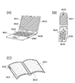
본 실시형태에서는, 액정 표시 장치의 외관 및 단면 등을 제시하며, 그 구성에 대해 설명한다. 본 실시형태에서는 표시 소자로서 액정 소자를 사용한 예를 들어 설명한다.In this embodiment, the external appearance, cross section, etc. of a liquid crystal display device are shown, and the structure is demonstrated. In this embodiment, the example which used the liquid crystal element as a display element is given and demonstrated.
또한, 액정 표시 장치란, 커넥터, 예를 들어 FPC(Flexible printed circuit) 또는 TCP(Tape Carrier Package)가 장착된 모듈, TCP의 끝에 프린트 배선판이 제공된 모듈, 또는 표시 소자에 COG(Chip On Glass) 방식에 의해 IC(집적 회로)가 직접 실장된 모듈도 모두 그 범주에 포함하는 것으로 한다.In addition, a liquid crystal display device is a connector, for example, a module equipped with a flexible printed circuit (FPC) or a tape carrier package (TCP), a module provided with a printed wiring board at the end of the TCP, or a chip on glass (COG) method in a display element. All modules in which ICs (integrated circuits) are mounted directly by this category are also included in the category.
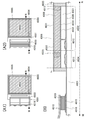
액정 표시 장치의 외관 및 단면에 대해, 도 9의 (A1), (A2), (B)를 사용하여 설명한다. 도 9의 (A1), (A2)는 제 1 기판(4001)과 제 2 기판(4006) 사이에 트랜지스터(4010, 4011), 및 액정 소자(4013)를 실재(4005)에 의해 밀봉한 패널의 평면도이며, 도 9의 (B)는 도 9의 (A1), (A2)의 M-N 부분의 단면도에 상당한다.The external appearance and cross section of a liquid crystal display device are demonstrated using FIG. 9 (A1), (A2), (B). 9A and 9A illustrate a panel in which
제 1 기판(4001) 위에 제공된 화소부(4002)와, 게이트 라인 구동 회로(4004)를 둘러싸도록 실재(4005)가 제공되어 있다. 또한 화소부(4002)와 게이트 라인 구동 회로(4004) 위에 제 2 기판(4006)이 제공되어 있다. 따라서, 화소부(4002)와 게이트 라인 구동 회로(4004)는 제 1 기판(4001)과 실재(4005)와 제 2 기판(4006)에 의해, 액정층(4008)과 함께 밀봉되어 있다. 또한 제 1 기판(4001) 위의 실재(4005)로 둘러싸여 있는 영역과는 다른 영역에, 별도 준비된 기판 위에 단결정 반도체막 또는 다결정 반도체막으로 형성된 소스 라인 구동 회로(4003)가 실장되어 있다.A
또한, 도 9에서는 도시하지 않았지만, 광원으로서 화소에 광을 조사하는 백 라이트를 적절히 제공할 수 있다. 여기서, 백 라이트는 상기 리셋 신호를 입력할 때, 비점등 상태인 것이 바람직하다. 이로써, 리셋 신호 입력에 따른 화상 왜곡의 표시를 방지할 수 있다. 또한, 도 9에서는 도시하지 않았지만, 설정한 시간에 상기 액정 표시 장치를 기동시키는 타이머를 적절히 제공할 수 있다. 여기서, 이 타이머는 액정 표시 장치가 사용되지 않는 특정한 시간(예를 들어, 심야 등 일반적으로 사용자가 액정 표시 장치를 사용하지 않는 시간 등)으로 설정하여 타이머로 액정 표시 장치를 기동시켜, 상기 리셋 신호를 입력시키면 좋다. 또한, 위상차판, 반사 방지막 등 광학 필름 등은 적절히 제공할 수 있다. 또한, 컬러 필터층으로서 기능하는 착색층을 제공할 수 있다.In addition, although not shown in FIG. 9, a backlight for irradiating light to the pixel as a light source can be appropriately provided. Here, the backlight is preferably in a non-lighting state when the reset signal is input. As a result, it is possible to prevent the display of the image distortion caused by the reset signal input. In addition, although not shown in FIG. 9, a timer for starting the liquid crystal display device at a set time can be appropriately provided. Here, the timer is set to a specific time when the liquid crystal display is not used (for example, a time when the user does not use the liquid crystal display in general, such as a late night, etc.) to start the liquid crystal display with a timer, and the reset signal. Is good. In addition, optical films, such as a retardation plate and an antireflection film, can be provided suitably. Moreover, the colored layer which functions as a color filter layer can be provided.
또한, 별도로 형성한 구동 회로의 접속 방식에 대해서는 특별한 한정은 없으며, COG 방식, 와이어 본딩 방식, 또는 TAB 방식 등을 이용할 수 있다. 도 9의 (A1)는 COG 방식에 의해 소스 라인 구동 회로(4003)를 실장하는 예이며, 도 9의 (A2)는 TAB 방식에 의해 소스 라인 구동 회로(4003)를 실장하는 예이다.In addition, the connection method of the drive circuit formed separately is not specifically limited, A COG system, a wire bonding system, a TAB system, etc. can be used. 9A is an example of mounting the source
또한, 제 1 기판(4001) 위에 제공된 화소부(4002)와, 게이트 라인 구동 회로(4004)는 복수의 트랜지스터를 가지며, 도 9의 (B)에서는 화소부(4002)에 포함되는 트랜지스터(4010)와 게이트 라인 구동 회로(4004)에 포함되는 트랜지스터(4011)를 예시하였다. 트랜지스터(4010, 4011) 위에는 절연층(4020, 4021)이 제공되어 있다.In addition, the
트랜지스터(4010, 4011)는 비정질, 미결정, 다결정, 또는 단결정인, 실리콘 또는 게르마늄 등 박막 반도체를 반도체층에 적용할 수 있다. 또는, 트랜지스터(4010, 4011)는 산화물 반도체를 반도체층에 적용할 수 있다. 본 실시형태에서, 트랜지스터(4010, 4011)는 n채널형 트랜지스터이다. 산화물 반도체를 반도체층에 적용함으로써, 오프 전류가 매우 낮은 트랜지스터를 화소의 스위칭 소자에 사용할 수 있다. 이 경우에는, 한 번 화소에 기록한 비디오 전압의 변동이 작기 때문에, 표시 품위의 향상을 도모할 수 있다.The
여기서, 전자 공여체(도너)가 되는 수분 또는 수소 등 불순물이 저감되고, 또 산소 결손이 저감됨으로써 고순도화된 산화물 반도체(purified OS)는 i형(진성 반도체)이거나, 또는 i형에 매우 가깝다. 그러므로, 고순도화된 산화물 반도체를 반도체층에 갖는 트랜지스터는 오프 전류가 매우 작고, 신뢰성이 높다.Here, an oxide semiconductor (purified OS) which is highly purified by reducing impurities such as moisture or hydrogen, which becomes an electron donor (donor), and reducing oxygen vacancies is an i type (intrinsic semiconductor) or very close to the i type. Therefore, the transistor having the highly purified oxide semiconductor in the semiconductor layer has a very low off current and high reliability.
구체적으로는, 고순도화된 산화물 반도체막에 채널 형성 영역을 갖는 트랜지스터의 오프 전류가 작다는 것은 여러 가지 실험에 의하여 증명할 수 있다. 예를 들어, 채널 폭이 1×106μm이고 채널 길이가 10μm인 소자의 경우에도, 소스 전극과 드레인 전극간의 전압(드레인 전압)이 1V 내지 10V인 범위에서 오프 전류가 반도체 파라미터 애널라이저의 측정 한계 이하, 즉 1×10-13A 이하라는 특성을 얻을 수 있다. 이 경우에, 오프 전류를 트랜지스터의 채널 폭으로 규격화한 오프 전류는 100zA/μm 이하인 것을 알 수 있다. 또한, 용량 소자와 트랜지스터를 접속시켜, 용량 소자에 유입 또는 용량 소자로부터 유출하는 전하를 상기 트랜지스터로 제어하는 회로를 사용하여, 오프 전류를 측정하였다. 상기 측정에서는 상기 트랜지스터에 고순도화된 산화물 반도체막을 채널 형성 영역에 사용하여, 용량 소자의 단위 시간당 전하량의 추이로부터 상기 트랜지스터의 오프 전류를 측정하였다. 이 결과로, 트랜지스터의 소스 전극과 드레인 전극간의 전압이 3V인 경우에, 수십 yA/μm라는, 더 작은 오프 전류가 얻어지는 것을 알았다. 따라서, 고순도화된 산화물 반도체막을 채널 형성 영역에 사용한 트랜지스터는 결정성을 갖는 실리콘을 사용한 트랜지스터에 비하여 오프 전류가 현저히 작다.Specifically, it can be proved by various experiments that the off current of the transistor having the channel formation region in the highly purified oxide semiconductor film is small. For example, in the case of a device having a channel width of 1 × 10 6 μm and a channel length of 10 μm, the off current is the measurement limit of the semiconductor parameter analyzer in the range where the voltage (drain voltage) between the source electrode and the drain electrode is 1V to 10V. In other words, 1 × 10 −13 A or less can be obtained. In this case, it can be seen that the off current obtained by normalizing the off current to the channel width of the transistor is 100 zA / μm or less. In addition, the off-current was measured using the circuit which connected the capacitor | condenser and transistor, and controls the electric charge which flows in or out of a capacitor | condenser by the said transistor. In this measurement, an oxide semiconductor film highly purified in the transistor was used for the channel formation region, and the off current of the transistor was measured from the change in the amount of charge per unit time of the capacitor. As a result, when the voltage between the source electrode and the drain electrode of a transistor is 3V, it turned out that smaller off current of several tens of yA / micrometer is obtained. Therefore, the transistor using the oxide semiconductor film of high purity in the channel forming region has a significantly smaller off current than the transistor using the crystalline silicon.
또한, 트랜지스터(4010, 4011)의 반도체층으로서 산화물 반도체막을 사용하는 경우, 산화물 반도체로서는 적어도 인듐(In) 또는 아연(Zn)을 포함하는 것이 바람직하다. 또한, 상기 산화물 반도체를 사용한 트랜지스터의 전기적 특성의 편차를 감소시키기 위한 스테빌라이저로서, 상술한 것에 추가하여 갈륨(Ga)을 갖는 것이 바람직하다. 또한, 스테빌라이저로서 주석(Sn)을 갖는 것이 바람직하다. 또한, 스테빌라이저로서 하프늄(Hf)을 갖는 것이 바람직하다. 또한, 스테빌라이저로서 알루미늄(Al)을 갖는 것이 바람직하다. 또한, 스테빌라이저로서 지르코늄(Zr)을 갖는 것이 바람직하다.In addition, when using an oxide semiconductor film as a semiconductor layer of
산화물 반도체 중에서도 In-Ga-Zn계 산화물, In-Sn-Zn계 산화물 등은 탄화 실리콘, 질화 갈륨, 또는 산화 갈륨과 달리, 스퍼터링법이나 습식법에 의해 전기적 특성이 우수한 트랜지스터를 제작할 수 있으며, 양산성이 우수하다는 이점이 있다. 또한, 탄화 실리콘, 질화 갈륨, 또는 산화 갈륨과 달리, 상기 In-Ga-Zn계 산화물은 유리 기판 위에 전기적 특성이 우수한 트랜지스터를 제작할 수 있다. 또한, 기판의 대형화에도 대응할 수 있다.Among the oxide semiconductors, in-Ga-Zn-based oxides, In-Sn-Zn-based oxides, and the like, unlike silicon carbide, gallium nitride, or gallium oxide, can produce transistors having excellent electrical characteristics by sputtering or wet method. There is an advantage that this is excellent. In addition, unlike silicon carbide, gallium nitride, or gallium oxide, the In—Ga—Zn-based oxide may fabricate a transistor having excellent electrical characteristics on a glass substrate. In addition, it is possible to cope with enlargement of the substrate.
또한, 다른 스테빌라이저로서 란타노이드인, 란탄(La), 세륨(Ce), 프라세오디뮴(Pr), 네오디뮴(Nd), 사마륨(Sm), 유로퓸(Eu), 가돌리늄(Gd), 테르븀(Tb), 디스프로슘(Dy), 홀뮴(Ho), 에르븀(Er), 툴륨(Tm), 이테르븀(Yb), 루테튬(Lu) 중 어느 한 종류 또는 복수 종류를 포함하여도 좋다.Other stabilizers include lanthanides, lanthanum (La), cerium (Ce), praseodymium (Pr), neodymium (Nd), samarium (Sm), europium (Eu), gadolinium (Gd), terbium (Tb), Any one or a plurality of types of dysprosium (Dy), holmium (Ho), erbium (Er), thulium (Tm), ytterbium (Yb) and lutetium (Lu) may be included.
예를 들어, 산화물 반도체로서, 산화 인듐, 산화 갈륨, 산화 주석, 산화 아연, 2원계 금속의 산화물인 In-Zn계 산화물, Sn-Zn계 산화물, Al-Zn계 산화물, Zn-Mg계 산화물, Sn-Mg계 산화물, In-Mg계 산화물, In-Ga계 산화물, 3원계 금속의 산화물인 In-Ga-Zn계 산화물(IGZO라고도 표기함), In-Al-Zn계 산화물, In-Sn-Zn계 산화물, Sn-Ga-Zn계 산화물, Al-Ga-Zn계 산화물, Sn-Al-Zn계 산화물, In-Hf-Zn계 산화물, In-La-Zn계 산화물, In-Pr-Zn계 산화물, In-Nd-Zn계 산화물, In-Sm-Zn계 산화물, In-Eu-Zn계 산화물, In-Gd-Zn계 산화물, In-Tb-Zn계 산화물, In-Dy-Zn계 산화물, In-Ho-Zn계 산화물, In-Er-Zn계 산화물, In-Tm-Zn계 산화물, In-Yb-Zn계 산화물, In-Lu-Zn계 산화물, 4원계 금속의 산화물인 In-Sn-Ga-Zn계 산화물, In-Hf-Ga-Zn계 산화물, In-Al-Ga-Zn계 산화물, In-Sn-Al-Zn계 산화물, In-Sn-Hf-Zn계 산화물, In-Hf-Al-Zn계 산화물을 사용할 수 있다.For example, indium oxide, gallium oxide, tin oxide, zinc oxide, In-Zn oxide, Sn-Zn oxide, Al-Zn oxide, Zn-Mg oxide, which are oxides of binary metal, Sn-Mg oxides, In-Mg oxides, In-Ga oxides, In-Ga-Zn oxides (also referred to as IGZO), oxides of ternary metals, In-Al-Zn oxides, In-Sn- Zn oxide, Sn-Ga-Zn oxide, Al-Ga-Zn oxide, Sn-Al-Zn oxide, In-Hf-Zn oxide, In-La-Zn oxide, In-Pr-Zn oxide Oxide, In-Nd-Zn oxide, In-Sm-Zn oxide, In-Eu-Zn oxide, In-Gd-Zn oxide, In-Tb-Zn oxide, In-Dy-Zn oxide, In-Ho-Zn-based oxides, In-Er-Zn-based oxides, In-Tm-Zn-based oxides, In-Yb-Zn-based oxides, In-Lu-Zn-based oxides, and oxides of quaternary metals In-Sn- Ga-Zn-based oxides, In-Hf-Ga-Zn-based oxides, In-Al-Ga-Zn-based oxides, In-Sn-Al-Zn-based oxides, In-Sn-Hf-Zn-based oxides, In-Hf- Al-Zn-based oxides can be used.
또한, 예를 들어, In-Ga-Zn계 산화물이란, In과 Ga와 Zn을 함유한 산화물을 뜻하며, In과 Ga와 Zn의 비율은 특별히 제한되지 않는다. 또한, In와 Ga와 Zn 이외의 금속 원소를 포함하여도 좋다. In-Ga-Zn계 산화물은 무(無)전계시의 저항이 충분히 높아 오프 전류를 충분히 작게 할 수 있으며, 또한 이동도도 높다.For example, an In—Ga—Zn-based oxide means an oxide containing In, Ga, and Zn, and the ratio of In, Ga, and Zn is not particularly limited. Moreover, you may contain metal elements other than In, Ga, and Zn. In-Ga-Zn-based oxides have a sufficiently high resistance in the absence of an electric field, which makes the off current sufficiently small, and also has high mobility.
예를 들어, 원자수비가 In:Ga:Zn=1:1:1(=1/3:1/3:1/3) 또는 In:Ga:Zn=2:2:1(=2/5:2/5:1/5)인 In-Ga-Zn계 산화물이나 이것과 근방의 조성을 갖는 산화물을 사용할 수 있다. 또는, 원자수비가 In:Sn:Zn=1:1:1(=1/3:1/3:1/3), In:Sn:Zn=2:1:3(=1/3:1/6:1/2) 또는 In:Sn:Zn=2:1:5(=1/4:1/8:5/8)인 In-Sn-Zn계 산화물이나 이것과 근방의 조성을 갖는 산화물을 사용하면 좋다.For example, the atomic ratio is In: Ga: Zn = 1: 1: 1 (= 1/3: 1/3: 1/3) or In: Ga: Zn = 2: 2: 1 (= 2/5: 2/5: 1/5) In-Ga-Zn-based oxide or an oxide having a composition close to this can be used. Alternatively, the atomic ratio is In: Sn: Zn = 1: 1: 1 (= 1/3: 1/3: 1/3), In: Sn: Zn = 2: 1: 3 (= 1/3: 1 / 6: 1/2) or In: Sn-Zn-based oxide having In: Sn: Zn = 2: 1: 5 (= 1/4: 1/8: 5/8), or an oxide having a composition close thereto. Do it.
예를 들어, In-Sn-Zn계 산화물은 비교적 용이하게 높은 이동도를 얻을 수 있다. 그러나, In-Ga-Zn계 산화물의 경우에도 벌크 내의 결함 밀도를 저감함으로써 이동도를 향상할 수 있다.For example, In—Sn—Zn-based oxides can obtain high mobility relatively easily. However, even in an In—Ga—Zn-based oxide, mobility can be improved by reducing the defect density in the bulk.
또한, 단결정, 다결정(폴리크리스탈이라고도 함), 또는 비정질 등의 상태를 갖는 산화물 반도체막을 트랜지스터에 사용할 수 있다. 바람직하게는, 산화물 반도체막은 CAAC-OS(C Axis Aligned Crystalline Oxide Semiconductor)막으로 한다.In addition, an oxide semiconductor film having a state such as single crystal, polycrystal (also called polycrystal), or amorphous can be used for the transistor. Preferably, the oxide semiconductor film is a CA Axis-O (C Axis Aligned Crystalline Oxide Semiconductor) film.
아래에서, 산화물 반도체막의 구조에 대해서 설명한다.Below, the structure of an oxide semiconductor film is demonstrated.
산화물 반도체막은 단결정 산화물 반도체막과, 비단결정 산화물 반도체막으로 대별된다. 비단결정 산화물 반도체막이란, 비정질 산화물 반도체막, 미결정 산화물 반도체막, 다결정 산화물 반도체막, CAAC-OS(C Axis Aligned Crystalline Oxide Semiconductor)막 등을 말한다.An oxide semiconductor film is roughly classified into a single crystal oxide semiconductor film and a non-single crystal oxide semiconductor film. The non-single crystal oxide semiconductor film refers to an amorphous oxide semiconductor film, a microcrystalline oxide semiconductor film, a polycrystalline oxide semiconductor film, a CAAC-OS (C Axis Aligned Crystalline Oxide Semiconductor) film, or the like.
비정질 산화물 반도체막은 막 내의 원자 배열이 불규칙하며, 결정 성분을 갖지 않는 산화물 반도체막이다. 미소 영역에도 결정부를 갖지 않고, 막 전체가 완전한 비정질 구조인 산화물 반도체막이 그 전형이다.An amorphous oxide semiconductor film is an oxide semiconductor film having an irregular atomic arrangement in the film and having no crystalline component. An oxide semiconductor film having no crystalline portion in a minute domain and having a complete amorphous structure as a whole is typical.
미결정 산화물 반도체막은 예를 들어, 크기가 1nm 이상 10nm 미만인 미결정(나노 결정이라고도 함)을 포함한다. 따라서, 미결정 산화물 반도체막은 비정질 산화물 반도체막보다 원자 배열의 규칙성이 높다. 그러므로, 미결정 산화물 반도체막은 비정질 산화물 반도체막보다 결함 준위 밀도가 낮다는 특징을 갖는다.The microcrystalline oxide semiconductor film includes, for example, microcrystalline (also referred to as nanocrystal) having a size of 1 nm or more and less than 10 nm. Therefore, the crystallinity of the microcrystalline oxide semiconductor film is higher than that of the amorphous oxide semiconductor film. Therefore, the microcrystalline oxide semiconductor film is characterized in that the defect level density is lower than that of the amorphous oxide semiconductor film.
CAAC-OS막은 복수의 결정부를 갖는 산화물 반도체막의 하나이며, 결정부의 대부분은 하나의 변이 100nm 미만인 입방체 내에 들어가는 크기이다. 따라서, CAAC-OS막에 포함되는 결정부는 하나의 변이 10nm 미만, 5nm 미만, 또는 3nm 미만인 입방체 내에 들어가는 크기인 경우도 포함된다. CAAC-OS막은 미결정 산화물 반도체막보다 결함 준위 밀도가 낮다는 특징을 갖는다. 아래에서 CAAC-OS막에 대하여 자세히 설명한다.The CAAC-OS film is one of oxide semiconductor films having a plurality of crystal parts, and most of the crystal parts are sized to fit into a cube whose one side is less than 100 nm. Therefore, the crystal portion included in the CAAC-OS film also includes a case in which one side is a size falling within a cube of less than 10 nm, less than 5 nm, or less than 3 nm. The CAAC-OS film has a feature that the defect level density is lower than that of the microcrystalline oxide semiconductor film. The CAAC-OS layer will be described in detail below.
CAAC-OS막을 투과형 전자 현미경(TEM: Transmission Electron Microscope)에 의하여 관찰하면, 결정부와 결정부 간의 명확한 경계, 즉 결정 입계(그레인 바운더리라고도 함)는 확인되지 않는다. 따라서, CAAC-OS막은 결정 입계에 기인하는 전자 이동도의 저하가 일어나기 어렵다고 할 수 있다.When the CAAC-OS film is observed by a transmission electron microscope (TEM), no clear boundary between the crystal part and the crystal part, that is, grain boundaries (also called grain boundaries) is not confirmed. Therefore, it can be said that the CAAC-OS film is less likely to lower the electron mobility due to the crystal grain boundaries.
CAAC-OS막을 시료면에 대략 평행한 방향으로부터 TEM에 의해 관찰(단면 TEM 관찰)하면, 결정부에서 금속 원자가 층상으로 배열되어 있는 것을 확인할 수 있다. 금속 원자의 각 층은 CAAC-OS막이 형성되는 면(피형성면이라고도 함) 또는 CAAC-OS막의 상면의 요철을 반영한 형상이며, CAAC-OS막의 피형성면 또는 상면에 평행하게 배열된다.When the CAAC-OS film is observed by TEM (cross-sectional TEM observation) from the direction substantially parallel to the sample surface, it can be confirmed that the metal atoms are arranged in layers in the crystal part. Each layer of the metal atoms reflects the surface on which the CAAC-OS film is formed (also called the surface to be formed) or the unevenness of the top surface of the CAAC-OS film, and is arranged parallel to the surface or top surface of the CAAC-OS film.
한편, CAAC-OS막을 시료면에 대략 수직인 방향으로부터 TEM에 의해 관찰(평면 TEM 관찰)하면, 결정부에서 금속 원자가 삼각형 또는 육각형으로 배열되어 있는 것을 확인할 수 있다. 그러나, 상이한 결정부 간에서 금속 원자의 배열에는 규칙성이 보이지 않는다.On the other hand, when the CAAC-OS film is observed by TEM (from a plane TEM observation) in a direction substantially perpendicular to the sample surface, it can be confirmed that the metal atoms are arranged in a triangular or hexagonal shape in the crystal part. However, there is no regularity in the arrangement of metal atoms between different crystal parts.
본 명세서에 있어서, '평행'이란, 2개의 직선이 -10° 이상 10° 이하의 각도로 배치된 상태를 말한다. 따라서, -5° 이상 5° 이하의 경우도 그 범주에 포함된다. 또한 '수직'이란, 2개의 직선이 80° 이상 100° 이하의 각도로 배치된 상태를 말한다. 따라서, 85° 이상 95° 이하의 경우도 그 범주에 포함된다.In this specification, "parallel" means the state in which two straight lines are arrange | positioned at the angle of -10 degrees or more and 10 degrees or less. Therefore, the range of -5 DEG to 5 DEG is also included in the category. The term " vertical " refers to a state in which two straight lines are disposed at angles of 80 DEG to 100 DEG. Therefore, the range of 85 degrees or more and 95 degrees or less is included in the category.
단면 TEM 관찰 및 평면 TEM 관찰에 의거하여, CAAC-OS막의 결정부는 배향성을 갖는 것을 알 수 있다.Based on cross-sectional TEM observation and planar TEM observation, it turns out that the crystal part of a CAAC-OS film has orientation.
X선 회절(XRD: X-Ray Diffraction) 장치를 사용하여 CAAC-OS막의 구조 해석을 수행하면, 예를 들어 InGaZnO4의 결정을 갖는 CAAC-OS막의 out-of-plane법에 의한 해석에서는, 회절각(2θ)의 피크가 31° 근방에 나타나는 경우가 있다. 이 피크는 InGaZnO4의 결정의 (009)면에 귀속되기 때문에, CAAC-OS막의 결정이 c축 배향성을 갖고, c축이 피형성면 또는 상면에 대략 수직인 방향으로 배향하는 것을 확인할 수 있다.When performing a structural analysis of a CAAC-OS film using an X-ray diffraction (XRD) apparatus, for example, in the analysis by the out-of-plane method of a CAAC-OS film having InGaZnO 4 crystals, The peak of the angle 2θ may appear around 31 °. Since this peak belongs to the (009) plane of the InGaZnO 4 crystal, it can be confirmed that the crystal of the CAAC-OS film has the c-axis orientation, and the c-axis is oriented in a direction substantially perpendicular to the formation surface or the upper surface.
한편, c축에 대략 수직인 방향으로부터 X선을 입사시키는 in-plane법에 의하여 CAAC-OS막을 해석하면, 2θ가 56° 근방일 때 피크가 나타나는 경우가 있다. 이 피크는 InGaZnO4의 결정의 (110)면에 귀속된다. InGaZnO4의 단결정 산화물 반도체막의 경우에는, 2θ를 56° 근방에 고정하여, 시료면의 법선 벡터를 축(φ축)으로 하여 시료를 회전시키면서 분석(φ 스캔)을 수행하면, (110)면과 등가인 결정면에 귀속되는 6개의 피크가 관찰된다. 한편, CAAC-OS막의 경우에는, 2θ를 56° 근방에 고정하여 φ 스캔을 수행하여도 명료한 피크가 나타나지 않는다.On the other hand, when the CAAC-OS film is analyzed by an in-plane method in which an X-ray is incident from a direction substantially perpendicular to the c-axis, a peak may appear when 2? This peak belongs to the (110) plane of the crystal of InGaZnO 4 . In the case of InGaZnO 4 single crystal oxide semiconductor film, when 2θ is fixed around 56 °, analysis (φ scan) is performed while rotating the sample with the normal vector of the sample plane as the axis (φ axis). Six peaks belonging to the equivalent crystal plane are observed. On the other hand, in the case of the CAAC-OS film, no clear peak is observed even if? Scan is performed by fixing 2?
따라서, CAAC-OS막에서는, 상이한 결정부 간에서 a축 및 b축의 배향이 불규칙하지만, c축 배향성을 갖고, 또 c축이 피형성면 또는 상면의 법선 벡터에 평행한 방향으로 배향하는 것을 알 수 있다. 따라서, 상술한 단면 TEM 관찰로 확인된 층상으로 배열된 금속 원자의 각층은 결정의 ab면에 평행한 면이다.Therefore, in the CAAC-OS film, although the a-axis and b-axis orientations are irregular between the different crystal portions, it is understood that the c-axis has alignment and the c-axis is oriented in a direction parallel to the normal vector of the surface to be formed or the upper surface. Can be. Therefore, each layer of the metal atoms arranged in the layer form confirmed by the above-described cross-sectional TEM observation is a plane parallel to the ab plane of the crystal.
또한, 결정부는 CAAC-OS막을 형성하였을 때 또는 열처리 등의 결정화 처리를 수행하였을 때에 형성된다. 상술한 바와 같이, 결정의 c축은 CAAC-OS막의 피형성면 또는 상면의 법선 벡터에 평행한 방향으로 배향한다. 따라서, 예를 들어 CAAC-OS막의 형상을 에칭 등에 의해 변화시킨 경우에는 결정의 c축이 CAAC-OS막의 피형성면 또는 상면의 법선 벡터에 평행하게 배향하지 않을 수도 있다.In addition, the crystal portion is formed when the CAAC-OS film is formed or when a crystallization process such as heat treatment is performed. As described above, the c-axis of the crystal aligns in the direction parallel to the normal vector on the surface to be formed or the upper surface of the CAAC-OS film. Therefore, for example, when the shape of the CAAC-OS film is changed by etching or the like, the c-axis of the crystal may not be oriented parallel to the normal vector of the formed surface or the upper surface of the CAAC-OS film.
또한, CAAC-OS막 내의 결정화도가 균일하지 않아도 좋다. 예를 들어, CAAC-OS막의 결정부가 CAAC-OS막의 상면 근방으로부터의 결정 성장에 의하여 형성되는 경우에는, 상면 근방의 영역은 피형성면 근방의 영역보다 결정화도가 높게 되는 경우가 있다. 또한, CAAC-OS막에 불순물을 첨가하는 경우에는, 불순물이 첨가된 영역의 결정화도가 변화되어, 부분적으로 결정화도가 다른 영역이 형성될 수도 있다.Further, the degree of crystallization in the CAAC-OS film need not be uniform. For example, when the crystal portion of the CAAC-OS film is formed by crystal growth from the vicinity of the top surface of the CAAC-OS film, the region near the top surface may have a higher degree of crystallinity than the region near the surface to be coated. In addition, when an impurity is added to the CAAC-OS film, the degree of crystallinity of the region to which the impurity is added may be changed, so that a region having a partially different degree of crystallinity may be formed.
또한, out-of-plane법에 의하여 InGaZnO4의 결정을 갖는 CAAC-OS막을 해석하면, 2θ의 피크가 31° 근방 외에 36° 근방에도 나타나는 경우가 있다. 2θ의 피크가 36° 근방에 나타나는 것은 CAAC-OS막 내의 일부에 c축 배향성을 갖지 않는 결정이 포함되는 것을 시사한다. CAAC-OS막은 2θ의 피크가 31° 근방에 나타나고, 36° 근방에 나타나지 않는 것이 바람직하다.In addition, when the CAAC-OS film having the InGaZnO 4 crystal is analyzed by the out-of-plane method, the peak of 2θ may appear in the vicinity of 36 ° in addition to the vicinity of 31 °. A peak at 2θ appearing around 36 ° suggests that a crystal having no c-axis orientation is included in a part of the CAAC-OS film. It is preferable that the peak of the 2? Appears in the vicinity of 31 DEG and does not appear in the vicinity of 36 DEG in the CAAC-OS film.
CAAC-OS막을 사용한 트랜지스터는 가시광이나 자외광의 조사에 기인한 전기 특성의 변동이 작다. 따라서, 상기 트랜지스터는 신뢰성이 높다.The transistor using the CAAC-OS film has a small variation in electric characteristics due to irradiation of visible light and ultraviolet light. Thus, the transistor is highly reliable.
또한, 산화물 반도체막은 예를 들어, 비정질 산화물 반도체막, 미결정 산화물 반도체막, CAAC-OS막 중 2종류 이상을 갖는 적층막이라도 좋다.The oxide semiconductor film may be a laminated film having two or more kinds of, for example, an amorphous oxide semiconductor film, a microcrystalline oxide semiconductor film, and a CAAC-OS film.
또한, 액정 소자(4013)가 갖는 화소 전극층(4030)은 박막 트랜지스터(4010)와 접속된다. 그리고, 액정 소자(4013)의 대향 전극층(4031)은 제 2 기판(4006) 위에 형성된다. 화소 전극층(4030)과 대향 전극층(4031)과 액정층(4008)이 중첩되는 부분이 액정 소자(4013)에 상당한다. 또한, 화소 전극층(4030), 대향 전극층(4031)은 각각 배향막으로서 기능하는 절연층(4032), 절연층(4033)이 제공되고, 절연층(4032), 절연층(4033)을 개재(介在)하여 액정층(4008)을 협지(挾持)한다.The
또한, 제 1 기판(4001), 제 2 기판(4006)으로서는, 투광성 기판을 사용할 수 있으며, 유리, 세라믹스, 플라스틱을 사용할 수 있다. 플라스틱으로서는, FRP(Fiberglass-Reinforced Plastics)판, PVF(폴리비닐플루오라이드) 필름, 폴리에스테르 필름, 또는 아크릴 수지 필름을 사용할 수 있다.As the
또한, 구조체(4035)는 절연막이 선택적으로 에칭되어 얻어지는 기둥 형상 스페이서이며, 화소 전극층(4030)과 대향 전극층(4031) 사이의 거리(셀 갭)를 제어하기 위해 제공된다. 또한, 구 형상의 스페이서를 사용하여도 좋다. 또한, 대향 전극층(4031)은 트랜지스터(4010)와 동일 기판 위에 제공되는 공통 전위선에 접속된다. 공통 접속부를 사용하여, 한 쌍의 기판간에 배치되는 도전성 입자를 통하여 대향 전극층(4031)과 공통 전위선을 접속할 수 있다. 한편, 도전성 입자는 실재(4005)에 함유시킬 수 있다.The
또한, 액정 소자의 전극의 구조는 액정 소자의 표시 모드에 의해 적절히 변경할 수 있다.In addition, the structure of the electrode of a liquid crystal element can be suitably changed with the display mode of a liquid crystal element.
또한, 액정 표시 장치에서는 기판의 외측(시인측)에 편광판을 제공하고, 내측에 착색층, 표시 소자에 이용하는 전극층의 순서로 제공하는 예를 나타내지만, 편광판은 기판의 내측에 제공하여도 좋다. 또한, 편광판과 착색층의 적층 구조도 본 실시형태에 한정되지 않으며, 편광판 및 착색층의 재료나 제작 공정 조건에 따라 적절히 설정하면 좋다. 또한, 표시부 이외에 블랙 매트릭스로서 기능하는 차광막을 제공하여도 좋다.In addition, although the liquid crystal display device provides the polarizing plate in the outer side (viewing side) of a board | substrate, and provides the inside in order of the colored layer and the electrode layer used for a display element, the polarizing plate may be provided inside a board | substrate. In addition, the laminated structure of a polarizing plate and a colored layer is not limited to this embodiment, What is necessary is just to set suitably according to the material and manufacturing process conditions of a polarizing plate and a colored layer. In addition to the display portion, a light shielding film functioning as a black matrix may be provided.
트랜지스터(4010) 및 트랜지스터(4011)는 반도체층 이외에, 게이트 절연층, 게이트 전극층, 및 배선층(소스 배선층이나 용량 배선층 등)으로 구성된다.The
또한, 트랜지스터(4010) 및 트랜지스터(4011) 위에 절연층(4020)이 형성된다. 절연층(4020)으로서는 일례로 RF 스퍼터링법에 의해 형성한 질화 실리콘막을 사용한다.In addition, an insulating
또한, 평탄화 절연막으로서 절연층(4021)을 형성한다. 절연층(4021)으로서는 폴리이미드, 아크릴, 벤조사이클로부텐계 수지, 폴리아미드, 에폭시 등 내열성을 갖는 유기 재료를 사용할 수 있다. 또한, 상기 유기 재료 이외에, 저유전율 재료(low-k 재료), 실록산계 수지, PSG(인 유리), BPSG(인붕소 유리) 등을 사용할 수 있다. 이때, 이들 재료로 형성되는 복수의 절연막을 적층시킴으로써, 절연층(4021)을 형성하여도 좋다.Further, an insulating
화소 전극층(4030), 대향 전극층(4031)에는 산화 텅스텐을 함유한 인듐 산화물, 산화 텅스텐을 함유한 인듐 아연 산화물, 산화 티타늄을 함유한 인듐 산화물, 산화 티타늄을 함유한 인듐 주석 산화물, 산화 인듐 주석, 인듐 아연 산화물, 산화 실리콘이 첨가된 인듐 주석 산화물 등 투광성을 갖는 도전성 재료를 사용할 수 있다.The
도전성 고분자로서는, 소위 π전자 공액계 도전성 고분자를 사용할 수 있다. 예를 들어, 폴리아닐린 또는 그 유도체, 폴리피롤 또는 그 유도체, 폴리티오펜 또는 그 유도체, 또는 아닐린, 피롤, 및 티오펜 중의 2종 이상으로 이루어진 공중합체 또는 그 유도체 등을 들 수 있다.As the conductive polymer, a so-called π-electron conjugated conductive polymer can be used. For example, the polyaniline or its derivative (s), polypyrrole or its derivative (s), polythiophene or its derivative (s), or the copolymer which consists of two or more of aniline, pyrrole, and thiophene, or its derivative (s), etc. are mentioned.
또한, 별도로 형성된 소스 라인 구동 회로(4003)와, 게이트 라인 구동 회로(4004) 또는 화소부(4002)에 공급되는 각종 신호 및 전위는 FPC(4018)로부터 공급된다.In addition, various signals and potentials supplied to the separately formed source
접속 단자 전극(4015)은 액정 소자(4013)에 포함된 화소 전극층(4030)과 같은 도전막으로 형성되고, 단자 전극(4016)은 박막 트랜지스터(4010), 트랜지스터(4011)의 소스 전극층 및 드레인 전극층과 같은 도전막으로 형성된다.The
접속 단자 전극(4015)은 이방성 도전막(4019)을 개재하여 FPC(4018)가 갖는 단자와 전기적으로 접속된다.The
또한, 도 9에서는 소스 라인 구동 회로(4003)를 별도로 형성하여 제 1 기판(4001)에 실장한 예를 도시하였지만, 본 실시형태는 이 구성에 한정되지 않는다. 게이트 라인 구동 회로를 별도 형성하여 실장하여도 좋고, 소스 라인 구동 회로의 일부 또는 게이트 라인 구동 회로의 일부만을 별도 형성하여 실장하여도 좋다.In addition, although the example which formed the source
본 실시형태는 다른 실시형태에 기재된 구성과 적절히 조합하여 실시할 수 있다.The present embodiment can be implemented in appropriate combination with the configuration described in the other embodiments.
(실시형태 3)(Embodiment 3)
본 실시형태에서는 실시형태 2에서 설명한 액정 소자의 표시 모드에 대해서 설명한다. 또한, 실시형태 2에서는 TN(Twisted Nematic) 모드의 단면이 되는 액정 소자의 일례를 도시하였지만, 다른 표시 모드로 할 수도 있다. 이하에서는, 각 표시 모드에서의 액정을 동작시키는 전극 및 기판에 대해서 모식도를 사용하여 설명한다.In this embodiment, the display mode of the liquid crystal element described in the second embodiment will be described. In addition, although the example of the liquid crystal element used as the cross section of TN (Twisted Nematic) mode was shown in
도 10은 TN 모드의 단면이 되는 액정 소자의 모식도이다.It is a schematic diagram of the liquid crystal element used as a cross section of TN mode.
서로 대향하도록 배치된 제 1 기판(5801) 및 제 2 기판(5802) 사이에 액정층(5800)이 협지된다. 제 1 기판(5801)에 제 1 전극(5805)이 형성된다. 제 2 기판(5802)에 제 2 전극(5806)이 형성된다.The
도 11의 (A)는 VA(Vertical Alignment) 모드의 액정 표시 장치의 단면의 모식도이다. VA 모드는 무전계일 때, 액정 분자가 기판에 수직이 되도록 배향되는 모드이다.FIG. 11A is a schematic view of a cross section of a liquid crystal display device in VA (Vertical Alignment) mode. The VA mode is a mode in which the liquid crystal molecules are oriented perpendicular to the substrate when in the field.
서로 대향하도록 배치된 제 1 기판(5811) 및 제 2 기판(5812) 사이에 액정층(5810)이 협지된다. 제 1 기판(5811)에 제 1 전극(5815)이 형성된다. 제 2 기판(5812)에 제 2 전극(5816)이 형성된다.The
도 11의 (B)는 MVA(Multi-domain Vertical Alignment) 모드의 액정 표시 장치의 단면의 모식도이다. MVA 모드는 돌기물을 제공함으로써, 복수 방향으로 액정 분자의 배향이 제어되어 시야각 의존성을 보상(補償)하는 방법이다.FIG. 11B is a schematic diagram of a cross section of a liquid crystal display device in a multi-domain vertical alignment (MVA) mode. The MVA mode is a method in which the alignment of liquid crystal molecules in a plurality of directions is controlled by providing a projection to compensate for the viewing angle dependency.
서로 대향하도록 배치된 제 1 기판(5821) 및 제 2 기판(5822) 사이에 액정층(5820)이 협지된다. 제 1 기판(5821)에 제 1 전극(5825)이 형성된다. 제 2 기판(5822)에 제 2 전극(5826)이 형성된다. 제 1 전극(5825) 위에는 배향 제어용으로 제 1 돌기물(5827)이 형성된다. 제 2 전극(5826) 위에는 배향 제어용으로 제 2 돌기물(5828)이 형성된다.The
도 12의 (A)는 IPS(In-Plane-Switching) 모드의 액정 표시 장치의 단면의 모식도이다. IPS 모드는 액정 분자를 기판에 대해 평행한 면 내에서 항상 회전시키는 모드이며, 화면을 보는 각도에 따른 액정층의 굴절률의 차이가 작기 때문에, 시야각 의존이 적다. IPS 모드는 전극을 한쪽 기판 측에만 제공한 수평 전계 방식을 채용한다.FIG. 12A is a schematic diagram of a cross section of a liquid crystal display device in an IPS (In-Plane-Switching) mode. The IPS mode is a mode in which the liquid crystal molecules are always rotated in a plane parallel to the substrate, and since the difference in refractive index of the liquid crystal layer according to the viewing angle is small, the viewing angle dependence is small. The IPS mode adopts a horizontal electric field system in which electrodes are provided only on one substrate side.
서로 대향하도록 배치된 제 1 기판(5851) 및 제 2 기판(5852) 사이에 액정층(5850)이 협지된다. 제 2 기판(5852)에 제 1 전극(5855) 및 제 2 전극(5856)이 형성된다.The
또한, IPS 모드 등의 수평 전계 방식의 전극 구조에서는 배향막을 사용하지 않는, 블루상을 나타내는 액정을 사용하여도 좋다.In addition, in the electrode structure of a horizontal electric field system, such as IPS mode, you may use the liquid crystal which shows a blue phase which does not use an alignment film.
도 12의 (B)는 FFS(Fringe Field Switching) 모드의 단면의 모식도이다. FFS 모드는 액정 분자를 기판에 대해 평행한 면 내에서 항상 회전시키는 모드이며, 화면을 보는 각도에 따른 액정층의 굴절률의 차이가 작기 때문에, 시야각 의존이 적다. FFS 모드는 전극을 한쪽 기판 측에만 제공한 수평 전계 방식을 채용한다.12B is a schematic diagram of a cross section of a FFS (Fringe Field Switching) mode. The FFS mode is a mode in which the liquid crystal molecules are always rotated in a plane parallel to the substrate, and since the difference in refractive index of the liquid crystal layer according to the viewing angle is small, the viewing angle dependence is small. The FFS mode adopts a horizontal electric field system in which electrodes are provided only on one substrate side.
서로 대향하도록 배치된 제 1 기판(5861) 및 제 2 기판(5862) 사이에 액정층(5860)이 협지된다. 제 2 기판(5862)에 제 2 전극(5866)이 형성된다. 제 2 전극(5866)에 절연막(5867)이 형성된다. 절연막(5867) 위에 제 1 전극(5865)이 형성된다.The liquid crystal layer 5560 is sandwiched between the first substrate 5601 and the second substrate 5586 disposed to face each other. The
본 실시형태는 다른 실시형태에 기재된 구성과 적절히 조합하여 실시하는 것이 가능하다.This embodiment can be implemented in appropriate combination with any of the structures described in the other embodiments.
(실시형태 4)(Fourth Embodiment)
본 실시형태에서는, 상술한 실시형태에서 설명한 액정 표시 장치를 구비하는 전자 기기에 대해서 설명한다. 전자 기기로서는, 텔레비전 수상기, 비디오 카메라, 디지털 카메라 등의 카메라, 고글형 디스플레이, 내비게이션 시스템, 음향 재생 장치(카오디오, 오디오 콤포넌트 등), 컴퓨터, 게임 기기, 휴대 정보 단말(모바일 컴퓨터, 휴대 전화, 스마트폰, 휴대형 오락기, 전자 서적, 또는 태블릿 단말 등), 기록 매체를 구비한 화상 재생 장치(구체적으로는 Digital Versatile Disc(DVD) 등의 기록 매체를 재생하고, 그 화상을 표시할 수 있는 표시 장치를 구비한 장치) 등을 들 수 있다. 이들 전자 기기의 구체적인 예에 대하여, 도 13 내지 도 15를 사용하여 설명한다.In this embodiment, an electronic device including the liquid crystal display device described in the above-described embodiment will be described. As an electronic device, cameras, such as a television receiver, a video camera, a digital camera, a goggle type display, a navigation system, a sound reproducing apparatus (car audio, an audio component, etc.), a computer, a game device, a portable information terminal (mobile computer, a mobile phone, A display device capable of playing back a recording medium such as a digital versatile disc (DVD) and displaying the image, including a smartphone, a portable entertainment device, an electronic book or a tablet terminal, and a recording medium. The apparatus provided with the above) is mentioned. Specific examples of these electronic devices will be described with reference to FIGS. 13 to 15.
도 13의 (A)는 휴대형 오락기이며, 하우징(9630), 표시부(9631), 스피커(9633), 조작 키(9635), 접속 단자(9636), 기록 매체 판독부(9672) 등을 구비할 수 있다. 도 13의 (A)의 휴대용 오락기는 기록 매체에 기록된 프로그램 또는 데이터를 판독하여 표시부에 표시하는 기능, 무선 통신에 의해 다른 휴대용 오락기와 정보를 공유하는 기능 등을 가질 수 있다. 도 13의 (A)에 도시된 휴대형 오락기의 기능은 이것에 한정되지 않으며, 다양한 기능을 가질 수 있다.FIG. 13A illustrates a portable entertainment device, and may include a
도 13의 (B)는 디지털 카메라이며, 하우징(9630), 표시부(9631), 스피커(9633), 조작 키(9635), 접속 단자(9636), 셔터 버튼(9676), 및 수상부(9677) 등을 구비할 수 있다. 도 13의 (B)의 디지털 카메라는 정지 화상을 촬영하는 기능, 동영상을 촬영하는 기능, 촬영된 화상을 자동적으로 또는 수동적으로 보정하는 기능, 촬영된 화상 등의 정보를 저장하는 기능, 촬영된 화상 등의 정보를 표시부에 표시하는 기능 등을 가질 수 있다. 도 13의 (B)에 도시된 디지털 카메라는 이것에 한정되지 않으며 다양한 기능을 가질 수 있다.FIG. 13B is a digital camera, which includes a
도 13의 (C)는 텔레비전 수상기이며, 하우징(9630), 표시부(9631), 스피커(9633), 조작 키(9635), 접속 단자(9636) 등을 구비할 수 있다. 도 13의 (C)의 텔레비전 수상기는 텔레비전용 전파를 화상 신호로 변환하는 기능, 화상 신호를 처리하여, 표시하는 데 적합한 신호로 변환하는 기능, 화상 신호의 프레임 주파수를 변환하는 기능 등을 가질 수 있다. 또한, 도 13의 (C)에 도시한 텔레비전 수상기가 갖는 기능은 이것에 한정되지 않으며, 다양한 기능을 가질 수 있다.FIG. 13C is a television receiver, and may include a
또한, 상술한 실시형태에서 설명한 바와 같이, 표시부(9631)의 화면 전체가 재기록되는 타이밍에 리셋 신호를 입력하는 구성으로 하는 경우에는, 채널이나 입력 장치를 전환할 때, 프로그램이 CF로 전환될 때 등에 리셋 신호를 입력하면 좋다.As described in the above-described embodiment, when the reset signal is input at the timing when the entire screen of the
도 14의 (A)는 컴퓨터이며, 하우징(9630), 표시부(9631), 스피커(9633), 조작 키(9635), 접속 단자(9636), 포인팅 디바이스(9681), 외부 접속 포트(9680) 등을 구비할 수 있다. 도 14의 (A)에 도시된 컴퓨터는 다양한 정보(정지 화상, 동영상, 및 텍스트 화상 등)를 표시부에 표시하는 기능, 다양한 소프트웨어(프로그램)에 의해 처리를 제어하는 기능, 무선 통신 또는 유선 통신 등의 통신 기능, 통신 기능을 이용하여 다양한 컴퓨터 네트워크에 접속하는 기능, 통신 기능을 이용하여 다양한 데이터를 송신 또는 수신하는 기능 등을 가질 수 있다. 또한, 도 14의 (A)의 컴퓨터가 갖는 기능은 이것에 한정되지 않으며, 다양한 기능을 가질 수 있다.14A illustrates a computer, which includes a
다음에, 도 14의 (B)는 휴대 전화이며, 하우징(9630), 표시부(9631), 스피커(9633), 조작 키(9635), 마이크로폰(9638), 외부 접속 포트(9680) 등을 구비할 수 있다. 도 14의 (B)에 도시된 휴대 전화는 다양한 정보(정지 화상, 동영상, 텍스트 화상 등)를 표시부에 표시하는 기능, 달력, 날짜, 또는 시간 등을 표시부에 표시하는 기능, 표시부에 표시된 정보를 조작하거나 편집하는 기능, 다양한 소프트웨어(프로그램)에 의해 처리를 제어하는 기능 등을 가질 수 있다. 또한, 도 14의 (B)에 도시된 휴대 전화가 갖는 기능은 이것에 한정되지 않으며, 다양한 기능을 가질 수 있다.Next, FIG. 14B is a mobile phone, and is provided with a
다음에, 도 14의 (C)는 전자 종이(E-book이라고도 함)이며, 하우징(9630), 표시부(9631), 조작 키(9635) 등을 구비할 수 있다. 도 14의 (C)에 도시된 전자 종이는 다양한 정보(정지 화상, 동영상, 텍스트 화상 등)를 표시부에 표시하는 기능, 달력, 날짜, 시간 등을 표시부에 표시하는 기능, 표시부에 표시된 정보를 조작하거나 편집하는 기능, 다양한 소프트웨어(프로그램)에 의해 처리를 제어하는 기능 등을 가질 수 있다. 또한, 도 14의 (C)에 도시된 전자 종이가 갖는 기능은 이것에 한정되지 않으며, 다양한 기능을 가질 수 있다.Next, FIG. 14C is an electronic paper (also referred to as an E-book), and may include a
도 15의 (A) 및 도 15의 (B)는 폴더형 태블릿 단말이다. 도 15의 (A)는 태블릿 단말을 펼친 상태이며, 하우징(9630), 표시부(9631a), 표시부(9631b), 표시 모드 전환 스위치(9624), 전원 스위치(9625), 전력 절약 모드 전환 스위치(9626), 후크(9623), 조작 스위치(9628)를 갖는다.15A and 15B are foldable tablet terminals. FIG. 15A is an open state of the tablet terminal, and includes a
표시부(9631a)는 일부를 터치 패널의 영역(9642a)으로 할 수 있고, 표시된 조작 키(9648)를 터치함으로써 데이터 입력을 할 수 있다. 또한, 도면에서는 일례로서 표시부(9631a)에 있어서 영역의 반이 표시만 하는 기능을 갖는 구성이고 영역의 나머지 반이 터치 패널 기능을 갖는 구성을 도시하였지만, 이 구성에 한정되지 않는다. 표시부(9631a)의 모든 영역이 터치 패널의 기능을 갖는 구성으로 하여도 좋다. 예를 들어, 표시부(9631a)의 전체 면에 키보드 버튼을 표시시켜 터치 패널로 하고, 표시부(9631b)를 표시 화면으로서 사용할 수 있다.The
또한, 표시부(9631b)에서도 표시부(9631a)와 마찬가지로, 표시부(9631b)의 일부를 터치 패널의 영역(9642b)으로 할 수 있다. 또한, 터치 패널의 키보드 표시 전환 버튼(9649)이 표시되어 있는 위치를 손가락이나 스타일러스 등으로 터치함으로써 표시부(9631b)에 키보드 버튼을 표시할 수 있다.In addition, similarly to the
또한, 터치 패널의 영역(9642a)과 터치 패널의 영역(9642b)에 대해 동시적으로 터치 입력을 수행할 수도 있다.In addition, touch input may be simultaneously performed on the area 9402a of the touch panel and the area 9964b of the touch panel.
또한, 표시 모드 전환 스위치(9624)는 세로 표시 또는 가로 표시 등의 표시 방향을 전환하거나, 흑백 표시나 컬러 표시의 전환 등을 선택할 수 있다. 전력 절약 모드 전환 스위치(9626)는 태블릿 단말에 내장되어 있는 광 센서로 검출되는 사용시의 외광의 광량에 따라 표시의 휘도를 최적의 것으로 할 수 있다. 태블릿 단말은 광 센서뿐만 아니라, 자이로, 가속도 센서 등 기울기를 검출하는 센서와 같은 다른 검출 장치를 내장하여도 좋다.In addition, the display
또한, 도 15의 (A)에서는 표시부(9631b)와 표시부(9631a)의 표시 면적이 같은 예를 도시하였지만, 이것에 특별히 한정되지 않으며, 크기가 서로 달라도 좋고 표시 품질도 달라도 좋다. 예를 들어, 한쪽이 다른 쪽보다 고정세한 표시가 가능한 표시 패널로 하여도 좋다.In addition, although the display area of the
도 15의 (B)는 태블릿 단말을 닫은 상태를 도시한 것이며, 하우징(9630), 태양 전지(9643), 충방전 제어 회로(9644), 배터리(9645), DCDC 컨버터(9646)를 구비한다. 또한, 도 15의 (B)에서는 충방전 제어 회로(9644)의 일례로서 배터리(9645), DCDC 컨버터(9646)를 구비하는 구성을 도시하였다.FIG. 15B illustrates a state in which the tablet terminal is closed, and includes a
또한, 태블릿 단말은 접을 수 있기 때문에, 사용하지 않을 때는 하우징(9630)을 닫은 상태로 할 수 있다. 따라서, 표시부(9631a), 표시부(9631b)를 보호할 수 있기 때문에, 내구성이 우수하며 장기 사용의 관점에서 보아도 신뢰성이 우수한 태블릿 단말을 제공할 수 있다.In addition, since the tablet terminal can be folded, the
또한, 이 외에도 도 15의 (A) 및 (B)에 도시된 태블릿 단말은 다양한 정보(정지 화상, 동영상, 텍스트 화상 등)를 표시하는 기능, 달력, 날짜, 또는 시각 등을 표시부에 표시하는 기능, 표시부에 표시한 정보를 터치 입력 조작하거나 또는 편집하는 터치 입력 기능, 각종 소프트웨어(프로그램)에 의하여 처리를 제어하는 기능 등을 가질 수 있다.In addition, the tablet terminal illustrated in FIGS. 15A and 15B may display a variety of information (still image, video, text image, etc.), and display a calendar, date, or time on the display unit. And a touch input function for touch input operation or editing of information displayed on the display unit, a function for controlling processing by various software (programs), and the like.
태블릿 단말의 표면에 장착된 태양 전지(9643)에 의하여, 터치 패널, 표시부, 또는 영상 신호 처리부 등에 전력을 공급할 수 있다. 또한, 태양 전지(9643)를 하우징(9630)의 한쪽 면 또는 양쪽 면에 제공할 수 있으며, 배터리(9645)를 효율적으로 충전할 수 있는 구성으로 할 수 있다. 또한 배터리(9645)로서 리튬 이온 전지를 사용하면, 소형화를 도모할 수 있는 등의 이점이 있다.The
또한, 도 15의 (B)에 도시된 충방전 제어 회로(9644)의 구성 및 동작에 대하여 도 15의 (C)에 블록도를 도시하여 설명한다. 도 15의 (C)는 태양 전지(9643), 배터리(9645), DCDC 컨버터(9646), 컨버터(9647), 스위치(SW1) 내지 스위치(SW3), 표시부(9631)를 도시한 것이며, 배터리(9645), DCDC 컨버터(9646), 컨버터(9647), 스위치(SW1) 내지 스위치(SW3)가 도 15의 (B)에 도시한 충방전 제어 회로(9644)에 대응하는 부분이다.In addition, the structure and operation of the charge /
먼저, 외광을 이용하여 태양 전지(9643)에 의해 발전되는 경우의 동작 예에 대해서 설명한다. 태양 전지(9643)로 발전한 전력은 배터리(9645)를 충전하기 위한 전압이 되도록 DCDC 컨버터(9646)로 승압 또는 강압이 수행된다. 그리고, 표시부(9631)의 동작에 태양 전지(9643)로부터의 전력이 사용될 때는 스위치(SW1)를 온 상태로 하여, 컨버터(9647)에 의해 표시부(9631)에 필요한 전압으로 승압 또는 강압을 수행한다. 또한, 표시부(9631)에서의 표시를 실시하지 않을 때는 스위치(SW1)를 오프 상태로 하고 스위치(SW2)를 온 상태로 하여 배터리(9645)를 충전하는 구성으로 하면 좋다.First, an operation example in the case of generating power by the
또한, 태양 전지(9643)에 대해서는 발전 수단의 일례로서 도시하였지만, 특별히 한정되지 않고 압전 소자(피에조 소자)나 열전 변환 소자(펠티어 소자) 등 다른 발전 수단에 의해 배터리(9645)를 충전하는 구성이라도 좋다. 예를 들어, 무선(비접촉)으로 전력을 송수신하여 충전하는 무접점 전력 전송 모듈이나, 다른 충전 수단을 조합하여 수행하는 구성으로 하여도 좋다.Although the
본 실시형태에 기재된 전자 기기는 상술한 실시형태에서 설명한 액정 표시 장치를 구비함으로써, 저소비 전력화를 도모할 수 있다.The electronic device described in this embodiment can achieve low power consumption by providing the liquid crystal display device described in the above-described embodiment.
본 실시형태는 다른 실시형태에 기재된 구성과 적절히 조합하여 실시할 수 있다.The present embodiment can be implemented in appropriate combination with the configuration described in the other embodiments.
100: 액정 표시 장치
101: 표시 제어 신호 생성 회로
102: 선택 회로
103: 표시 패널
104: 게이트 라인 구동 회로
105: 소스 라인 구동 회로
106: 화소부
107: 디지털/아날로그 변환 회로
108: 화소
109: 게이트 라인
110: 소스 라인
201: 시프트 레지스터 회로
202: 시프트 레지스터 회로
203: 아날로그 스위치
204: 트랜지스터
205: 용량 소자
206: 액정 소자
211: 화소
212: 화소
213: 화소
221: 화소
222: 화소
223: 화소
231: 화소
232: 화소
233: 화소
4001: 기판
4002: 화소부
4003: 소스 라인 구동 회로
4004: 게이트 라인 구동 회로
4005: 실재
4006: 기판
4008: 액정층
4010: 트랜지스터
4011: 트랜지스터
4013: 액정 소자
4015: 접속 단자 전극
4016: 단자 전극
4018: FPC
4019: 이방성 도전막
4020: 절연층
4021: 절연층
4030: 화소 전극층
4031: 대향 전극층
4032: 절연층
4033: 절연층
4035: 구조체
5800: 액정층
5801: 기판
5802: 기판
5805: 전극
5806: 전극
5810: 액정층
5811: 기판
5812: 기판
5815: 전극
5816: 전극
5820: 액정층
5821: 기판
5822: 기판
5825: 전극
5826: 전극
5827: 돌기물
5828: 돌기물
5850: 액정층
5851: 기판
5852: 기판
5855: 전극
5856: 전극
5860: 액정층
5861: 기판
5862: 기판
5865: 전극
5866: 전극
5867: 절연막
9623: 후크
9624: 스위치
9625: 전원 스위치
9626: 스위치
9628: 조작 스위치
9630: 하우징
9631: 표시부
9631a: 표시부
9631b: 표시부
9633: 스피커
9635: 조작 키
9636: 접속 단자
9638: 마이크로폰
9642a: 영역
9642b: 영역
9643: 태양 전지
9644: 충방전 제어 회로
9645: 배터리
9646: DCDC 컨버터
9647: 컨버터
9648: 조작 키
9649: 버튼
9672: 기록 매체 판독부
9676: 셔터 버튼
9677: 수상부
9680: 외부 접속 포트
9681: 포인팅 디바이스100: liquid crystal display
101: display control signal generation circuit
102: selection circuit
103: display panel
104: gate line driving circuit
105: source line driving circuit
106:
107: digital to analog conversion circuit
108: pixels
109: gate line
110: source line
201: shift register circuit
202: shift register circuit
203: analog switch
204: transistor
205: Capacitive element
206: liquid crystal element
211 pixels
212 pixels
213 pixels
221 pixels
222 pixels
223 pixels
231 pixels
232: pixels
233 pixels
4001: substrate
4002:
4003: source line drive circuit
4004: gate line driving circuit
4005: Real
4006: substrate
4008: liquid crystal layer
4010: transistor
4011: transistor
4013: liquid crystal element
4015: connecting terminal electrode
4016: terminal electrode
4018: FPC
4019: anisotropic conductive film
4020: Insulation layer
4021: insulation layer
4030: pixel electrode layer
4031: counter electrode layer
4032: insulation layer
4033: insulation layer
4035: structure
5800: liquid crystal layer
5801: substrate
5802: substrate
5805: electrode
5806: electrode
5810 liquid crystal layer
5811: substrate
5812: substrate
5815: electrode
5816: electrode
5820: liquid crystal layer
5821: substrate
5822: substrate
5825: electrode
5826: electrode
5827: projection
5828: projection
5850: liquid crystal layer
5851: substrate
5852: substrate
5855: electrode
5856: electrode
5860 liquid crystal layer
5861: substrate
5862: substrate
5865: electrode
5866: electrode
5867: insulating film
9623: hook
9624: switch
9625: power switch
9626: switch
9628: operation switch
9630: Housing
9631:
9631a:
9631b:
9633: speaker
9635: operation keys
9636: connection terminal
9638: microphone
9642a: area
9642b: area
9643: solar cells
9644: charge and discharge control circuit
9645: battery
9646: DCDC converter
9647: Converter
9648: Operation keys
9649: button
9672: recording medium reading unit
9676: Shutter Button
9677: award
9680: external connection port
9681: pointing device
Claims (16)
액정 소자를 포함하는 화소와;
비디오 신호의 극성을 m프레임(m은 2 이상의 자연수)마다 반전시키면서 상기 비디오 신호를 상기 화소에 입력하고, 상기 비디오 신호가 상기 화소에 입력되지 않을 때에 리셋 신호를 상기 화소에 입력하는 구동 회로를 포함하는, 액정 표시 장치.In a liquid crystal display device,
A pixel including a liquid crystal element;
A driving circuit for inputting the video signal to the pixel while inverting the polarity of the video signal every m frames (m is a natural number of two or more), and inputting a reset signal to the pixel when the video signal is not input to the pixel. Liquid crystal display device.
상기 리셋 신호의 전위는 제 1 기간에는 공통 전위보다 높고, 제 2 기간에는 상기 공통 전위보다 낮은, 액정 표시 장치.The method of claim 1,
The potential of the reset signal is higher than the common potential in the first period and lower than the common potential in the second period.
상기 리셋 신호의 상기 전위는 상기 제 1 기간 및 상기 제 2 기간 후에는 상기 공통 전위와 대략 같은 전위인, 액정 표시 장치.3. The method of claim 2,
And the potential of the reset signal is a potential approximately equal to the common potential after the first and second periods.
상기 화소에 대해 광을 발광할 수 있는 백 라이트를 더 포함하고,
상기 구동 회로는 상기 백 라이트가 발광하지 않을 때에 상기 리셋 신호를 상기 화소에 입력하는, 액정 표시 장치.The method of claim 1,
Further comprising a backlight capable of emitting light to the pixel,
And the driving circuit inputs the reset signal to the pixel when the backlight does not emit light.
액정 소자 및 상기 액정 소자에 전기적으로 접속된 트랜지스터를 포함하는 화소와;
비디오 신호의 극성을 m프레임(m은 2 이상의 자연수)마다 반전시키면서 상기 비디오 신호를 상기 화소에 입력하고, 상기 비디오 신호가 상기 화소에 입력되지 않을 때에 리셋 신호를 상기 화소에 입력하는 구동 회로를 포함하고,
상기 트랜지스터는 채널 형성 영역을 포함하는 산화물 반도체층을 포함하는, 액정 표시 장치.In a liquid crystal display device,
A pixel including a liquid crystal element and a transistor electrically connected to the liquid crystal element;
And a driving circuit for inputting the video signal to the pixel while inverting the polarity of the video signal every m frames (m is a natural number of two or more), and inputting a reset signal to the pixel when the video signal is not input to the pixel. and,
And the transistor comprises an oxide semiconductor layer including a channel formation region.
상기 리셋 신호의 전위는 제 1 기간에는 공통 전위보다 높고, 제 2 기간에는 상기 공통 전위보다 낮은, 액정 표시 장치.The method of claim 5, wherein
The potential of the reset signal is higher than the common potential in the first period and lower than the common potential in the second period.
상기 리셋 신호의 상기 전위는 상기 제 1 기간 및 상기 제 2 기간 후에는 상기 공통 전위와 대략 같은 전위인, 액정 표시 장치.The method according to claim 6,
And the potential of the reset signal is a potential approximately equal to the common potential after the first and second periods.
상기 화소에 대해 광을 발광할 수 있는 백 라이트를 더 포함하고,
상기 구동 회로는 상기 백 라이트가 발광하지 않을 때에 상기 리셋 신호를 상기 화소에 입력하는, 액정 표시 장치.The method of claim 5, wherein
Further comprising a backlight capable of emitting light to the pixel,
And the driving circuit inputs the reset signal to the pixel when the backlight does not emit light.
트랜지스터 및 상기 트랜지스터에 전기적으로 접속된 액정 소자를 각각 포함하는 복수의 화소와;
상기 복수의 화소 각각에 비디오 신호 및 리셋 신호를 입력하는 구동 회로를 포함하고,
상기 구동 회로는 상기 비디오 신호의 극성을 m프레임(m은 2 이상의 자연수)마다 반전시키면서 상기 비디오 신호를 상기 복수의 화소 각각에 입력하고,
상기 구동 회로는 상기 비디오 신호가 입력되지 않는 기간에 상기 리셋 신호를 상기 복수의 화소 각각에 입력하는, 액정 표시 장치.In a liquid crystal display device,
A plurality of pixels each including a transistor and a liquid crystal element electrically connected to the transistor;
A driving circuit for inputting a video signal and a reset signal to each of the plurality of pixels;
The driving circuit inputs the video signal to each of the plurality of pixels while inverting the polarity of the video signal every m frames (m is a natural number of two or more),
And the driving circuit inputs the reset signal to each of the plurality of pixels in a period when the video signal is not input.
상기 구동 회로는 상기 리셋 신호를 상기 복수의 화소 각각에 입력하고, 상기 리셋 신호의 전위는 상기 전위가 공통 전위보다 높은 기간 및 상기 전위가 상기 공통 전위보다 낮은 기간이 적어도 한 번 반복된 후에, 상기 공통 전위와 대략 같은 전위인, 액정 표시 장치.The method of claim 9,
The driving circuit inputs the reset signal to each of the plurality of pixels, and the potential of the reset signal is repeated after at least one time period in which the potential is higher than the common potential and the period in which the potential is lower than the common potential is repeated. A liquid crystal display device, which is about the same potential as the common potential.
상기 액정 소자는 한 쌍의 전극을 포함하고,
상기 리셋 신호를 입력함으로써 상기 액정 소자의 상기 한 쌍의 전극 사이의 전위차를 대략 0V로 한 후, 상기 트랜지스터가 오프 상태가 되는, 액정 표시 장치.The method of claim 9,
The liquid crystal device includes a pair of electrodes,
The transistor is turned off after the potential difference between the pair of electrodes of the liquid crystal element is approximately 0 V by inputting the reset signal.
상기 구동 회로가 상기 리셋 신호를 상기 복수의 화소 모두에 입력한 후, 전원 공급이 차단되는, 액정 표시 장치.The method of claim 9,
And the power supply is cut off after the driving circuit inputs the reset signal to all of the plurality of pixels.
상기 복수의 화소에 대해 광을 발광할 수 있는 백 라이트를 더 포함하고,
상기 구동 회로는 상기 백 라이트가 발광하지 않을 때에 상기 리셋 신호를 상기 복수의 화소 각각에 입력하는, 액정 표시 장치.The method of claim 9,
Further comprising a backlight for emitting light to the plurality of pixels,
And the driving circuit inputs the reset signal to each of the plurality of pixels when the backlight does not emit light.
상기 구동 회로는 상기 화소 모두에서 데이터가 재기록됨과 동시에 상기 리셋 신호를 상기 복수의 화소 각각에 입력하는, 액정 표시 장치.The method of claim 9,
And the driving circuit inputs the reset signal to each of the plurality of pixels while simultaneously rewriting data in all of the pixels.
설정 시간에 상기 액정 표시 장치를 기동시키는 타이머를 더 포함하고,
상기 구동 회로는 상기 액정 표시 장치가 상기 타이머에 의해 전원 오프 상태로부터 기동되었을 때, 상기 리셋 신호를 상기 복수의 화소 각각에 입력하는, 액정 표시 장치.The method of claim 9,
A timer for starting the liquid crystal display at a set time;
And the driving circuit inputs the reset signal to each of the plurality of pixels when the liquid crystal display is started from the power-off state by the timer.
상기 트랜지스터는 산화물 반도체를 포함하는, 액정 표시 장치.The method of claim 9,
And the transistor comprises an oxide semiconductor.
Applications Claiming Priority (2)
| Application Number | Priority Date | Filing Date | Title |
|---|---|---|---|
| JP2012165630 | 2012-07-26 | ||
| JPJP-P-2012-165630 | 2012-07-26 |
Publications (1)
| Publication Number | Publication Date |
|---|---|
| KR20140013931A true KR20140013931A (en) | 2014-02-05 |
Family
ID=49994414
Family Applications (1)
| Application Number | Title | Priority Date | Filing Date |
|---|---|---|---|
| KR1020130082985A KR20140013931A (en) | 2012-07-26 | 2013-07-15 | Liquid crystal display device |
Country Status (5)
| Country | Link |
|---|---|
| US (1) | US9390664B2 (en) |
| JP (2) | JP2014041348A (en) |
| KR (1) | KR20140013931A (en) |
| CN (1) | CN103578442B (en) |
| TW (1) | TWI588808B (en) |
Families Citing this family (7)
| Publication number | Priority date | Publication date | Assignee | Title |
|---|---|---|---|---|
| JP2014032399A (en) | 2012-07-13 | 2014-02-20 | Semiconductor Energy Lab Co Ltd | Liquid crystal display device |
| US9984644B2 (en) | 2012-08-08 | 2018-05-29 | Semiconductor Energy Laboratory Co., Ltd. | Liquid crystal display device and method for driving the same |
| WO2014185122A1 (en) * | 2013-05-15 | 2014-11-20 | シャープ株式会社 | Liquid crystal display device |
| JP2018013765A (en) | 2016-04-28 | 2018-01-25 | 株式会社半導体エネルギー研究所 | Electronic device |
| JP2018040963A (en) * | 2016-09-08 | 2018-03-15 | ラピスセミコンダクタ株式会社 | Display driver and display device |
| DE112018002240T5 (en) * | 2017-04-27 | 2020-01-09 | Semiconductor Energy Laboratory Co., Ltd. | Display unit, display device and electronic device |
| JP6798470B2 (en) * | 2017-11-08 | 2020-12-09 | カシオ計算機株式会社 | Electronic clocks, display control methods, and programs |
Family Cites Families (165)
| Publication number | Priority date | Publication date | Assignee | Title |
|---|---|---|---|---|
| JPS60198861A (en) | 1984-03-23 | 1985-10-08 | Fujitsu Ltd | Thin film transistor |
| JPH0244256B2 (en) | 1987-01-28 | 1990-10-03 | Kagaku Gijutsucho Mukizaishitsu Kenkyushocho | INGAZN2O5DESHIMESARERUROTSUHOSHOKEINOSOJOKOZOOJUSURUKAGOBUTSUOYOBISONOSEIZOHO |
| JPS63210023A (en) | 1987-02-24 | 1988-08-31 | Natl Inst For Res In Inorg Mater | Compound having laminar structure of hexagonal crystal system expressed by ingazn4o7 and its production |
| JPH0244260B2 (en) | 1987-02-24 | 1990-10-03 | Kagaku Gijutsucho Mukizaishitsu Kenkyushocho | INGAZN5O8DESHIMESARERUROTSUHOSHOKEINOSOJOKOZOOJUSURUKAGOBUTSUOYOBISONOSEIZOHO |
| JPH0244258B2 (en) | 1987-02-24 | 1990-10-03 | Kagaku Gijutsucho Mukizaishitsu Kenkyushocho | INGAZN3O6DESHIMESARERUROTSUHOSHOKEINOSOJOKOZOOJUSURUKAGOBUTSUOYOBISONOSEIZOHO |
| JPH0244262B2 (en) | 1987-02-27 | 1990-10-03 | Kagaku Gijutsucho Mukizaishitsu Kenkyushocho | INGAZN6O9DESHIMESARERUROTSUHOSHOKEINOSOJOKOZOOJUSURUKAGOBUTSUOYOBISONOSEIZOHO |
| JPH0244263B2 (en) | 1987-04-22 | 1990-10-03 | Kagaku Gijutsucho Mukizaishitsu Kenkyushocho | INGAZN7O10DESHIMESARERUROTSUHOSHOKEINOSOJOKOZOOJUSURUKAGOBUTSUOYOBISONOSEIZOHO |
| JPH05251705A (en) | 1992-03-04 | 1993-09-28 | Fuji Xerox Co Ltd | Thin-film transistor |
| JPH08179728A (en) * | 1994-12-21 | 1996-07-12 | Sharp Corp | Liquid crystal display device |
| JP3479375B2 (en) | 1995-03-27 | 2003-12-15 | 科学技術振興事業団 | Metal oxide semiconductor device in which a pn junction is formed with a thin film transistor made of a metal oxide semiconductor such as cuprous oxide, and methods for manufacturing the same |
| US5900886A (en) | 1995-05-26 | 1999-05-04 | National Semiconductor Corporation | Display controller capable of accessing an external memory for gray scale modulation data |
| US5821910A (en) | 1995-05-26 | 1998-10-13 | National Semiconductor Corporation | Clock generation circuit for a display controller having a fine tuneable frame rate |
| EP0820644B1 (en) | 1995-08-03 | 2005-08-24 | Koninklijke Philips Electronics N.V. | Semiconductor device provided with transparent switching element |
| JP3625598B2 (en) | 1995-12-30 | 2005-03-02 | 三星電子株式会社 | Manufacturing method of liquid crystal display device |
| KR100272723B1 (en) | 1996-06-06 | 2000-11-15 | 니시무로 타이죠 | Flat panel display device |
| JPH10111491A (en) * | 1996-10-08 | 1998-04-28 | Fujitsu Ltd | Liquid crystal display device |
| JPH10293286A (en) | 1997-02-21 | 1998-11-04 | Toshiba Corp | Driving method for liquid crystal display device |
| KR100266212B1 (en) | 1997-05-17 | 2000-09-15 | 구본준; 론 위라하디락사 | Lcd with the function of removing residual image |
| JPH1124041A (en) * | 1997-06-30 | 1999-01-29 | Toshiba Corp | Liquid crystal display device |
| US6496172B1 (en) | 1998-03-27 | 2002-12-17 | Semiconductor Energy Laboratory Co., Ltd. | Liquid crystal display device, active matrix type liquid crystal display device, and method of driving the same |
| JP2000081606A (en) | 1998-06-29 | 2000-03-21 | Sanyo Electric Co Ltd | Method for driving liquid crystal display element |
| JP4170454B2 (en) | 1998-07-24 | 2008-10-22 | Hoya株式会社 | Article having transparent conductive oxide thin film and method for producing the same |
| JP2000150861A (en) | 1998-11-16 | 2000-05-30 | Tdk Corp | Oxide thin film |
| JP3276930B2 (en) | 1998-11-17 | 2002-04-22 | 科学技術振興事業団 | Transistor and semiconductor device |
| JP3589395B2 (en) | 1999-03-29 | 2004-11-17 | シャープ株式会社 | Liquid crystal display |
| JP3466951B2 (en) * | 1999-03-30 | 2003-11-17 | 株式会社東芝 | Liquid crystal display |
| TW460731B (en) | 1999-09-03 | 2001-10-21 | Ind Tech Res Inst | Electrode structure and production method of wide viewing angle LCD |
| JP4519251B2 (en) * | 1999-10-13 | 2010-08-04 | シャープ株式会社 | Liquid crystal display device and control method thereof |
| TW494382B (en) | 2000-03-22 | 2002-07-11 | Toshiba Corp | Display apparatus and driving method of display apparatus |
| EP1296174B1 (en) | 2000-04-28 | 2016-03-09 | Sharp Kabushiki Kaisha | Display unit, drive method for display unit, electronic apparatus mounting display unit thereon |
| JP4089858B2 (en) | 2000-09-01 | 2008-05-28 | 国立大学法人東北大学 | Semiconductor device |
| JP2002107769A (en) * | 2000-09-29 | 2002-04-10 | Toshiba Corp | Liquid crystal display element and method for aligning liquid crystal |
| JP3842030B2 (en) | 2000-10-06 | 2006-11-08 | シャープ株式会社 | Active matrix display device and driving method thereof |
| KR20020038482A (en) | 2000-11-15 | 2002-05-23 | 모리시타 요이찌 | Thin film transistor array, method for producing the same, and display panel using the same |
| JP2002229532A (en) | 2000-11-30 | 2002-08-16 | Toshiba Corp | Liquid crystal display and its driving method |
| JP3607197B2 (en) | 2000-12-26 | 2005-01-05 | シャープ株式会社 | Display drive device and display device module |
| JP3730159B2 (en) | 2001-01-12 | 2005-12-21 | シャープ株式会社 | Display device driving method and display device |
| JP4879427B2 (en) | 2001-02-21 | 2012-02-22 | 株式会社半導体エネルギー研究所 | Liquid crystal display |
| JP3997731B2 (en) | 2001-03-19 | 2007-10-24 | 富士ゼロックス株式会社 | Method for forming a crystalline semiconductor thin film on a substrate |
| JP2002289859A (en) | 2001-03-23 | 2002-10-04 | Minolta Co Ltd | Thin-film transistor |
| JP3916986B2 (en) * | 2001-05-18 | 2007-05-23 | シャープ株式会社 | Signal processing circuit, low-voltage signal generator, and image display device including the same |
| JP2002351430A (en) | 2001-05-30 | 2002-12-06 | Mitsubishi Electric Corp | Display device |
| GB2378343B (en) | 2001-08-03 | 2004-05-19 | Sendo Int Ltd | Image refresh in a display |
| JP4090716B2 (en) | 2001-09-10 | 2008-05-28 | 雅司 川崎 | Thin film transistor and matrix display device |
| JP3925839B2 (en) | 2001-09-10 | 2007-06-06 | シャープ株式会社 | Semiconductor memory device and test method thereof |
| JP4164562B2 (en) | 2002-09-11 | 2008-10-15 | 独立行政法人科学技術振興機構 | Transparent thin film field effect transistor using homologous thin film as active layer |
| WO2003040441A1 (en) | 2001-11-05 | 2003-05-15 | Japan Science And Technology Agency | Natural superlattice homologous single crystal thin film, method for preparation thereof, and device using said single crystal thin film |
| JP3627710B2 (en) | 2002-02-14 | 2005-03-09 | セイコーエプソン株式会社 | Display drive circuit, display panel, display device, and display drive method |
| JP4083486B2 (en) | 2002-02-21 | 2008-04-30 | 独立行政法人科学技術振興機構 | Method for producing LnCuO (S, Se, Te) single crystal thin film |
| US7023141B2 (en) * | 2002-03-01 | 2006-04-04 | Semiconductor Energy Laboratory Co., Ltd. | Light emitting device and drive method thereof |
| US7049190B2 (en) | 2002-03-15 | 2006-05-23 | Sanyo Electric Co., Ltd. | Method for forming ZnO film, method for forming ZnO semiconductor layer, method for fabricating semiconductor device, and semiconductor device |
| JP3933591B2 (en) | 2002-03-26 | 2007-06-20 | 淳二 城戸 | Organic electroluminescent device |
| US7339187B2 (en) | 2002-05-21 | 2008-03-04 | State Of Oregon Acting By And Through The Oregon State Board Of Higher Education On Behalf Of Oregon State University | Transistor structures |
| JP2004022625A (en) | 2002-06-13 | 2004-01-22 | Murata Mfg Co Ltd | Manufacturing method of semiconductor device and its manufacturing method |
| US7105868B2 (en) | 2002-06-24 | 2006-09-12 | Cermet, Inc. | High-electron mobility transistor with zinc oxide |
| US7067843B2 (en) | 2002-10-11 | 2006-06-27 | E. I. Du Pont De Nemours And Company | Transparent oxide semiconductor thin film transistors |
| JP4421559B2 (en) * | 2003-01-08 | 2010-02-24 | 東芝モバイルディスプレイ株式会社 | Liquid crystal display |
| JP4166105B2 (en) | 2003-03-06 | 2008-10-15 | シャープ株式会社 | Semiconductor device and manufacturing method thereof |
| JP2004273732A (en) | 2003-03-07 | 2004-09-30 | Sharp Corp | Active matrix substrate and its producing process |
| JP4108633B2 (en) | 2003-06-20 | 2008-06-25 | シャープ株式会社 | THIN FILM TRANSISTOR, MANUFACTURING METHOD THEREOF, AND ELECTRONIC DEVICE |
| US7262463B2 (en) | 2003-07-25 | 2007-08-28 | Hewlett-Packard Development Company, L.P. | Transistor including a deposited channel region having a doped portion |
| TWI293750B (en) | 2003-10-02 | 2008-02-21 | Sanyo Electric Co | Method for driving a liquid crystal display device, a liquid crystal display device, and a driving device for such liquid crystal device |
| JP2005157157A (en) * | 2003-11-28 | 2005-06-16 | Toppoly Optoelectronics Corp | Residual video removing electric circuit |
| JP4016942B2 (en) | 2003-12-10 | 2007-12-05 | セイコーエプソン株式会社 | PWM signal generation circuit and display driver |
| KR101078483B1 (en) | 2004-03-12 | 2011-10-31 | 도꾸리쯔교세이호징 가가꾸 기쥬쯔 신꼬 기꼬 | Switching device of lcd or organic electro luminescence display |
| US7282782B2 (en) | 2004-03-12 | 2007-10-16 | Hewlett-Packard Development Company, L.P. | Combined binary oxide semiconductor device |
| US7145174B2 (en) | 2004-03-12 | 2006-12-05 | Hewlett-Packard Development Company, Lp. | Semiconductor device |
| US7297977B2 (en) | 2004-03-12 | 2007-11-20 | Hewlett-Packard Development Company, L.P. | Semiconductor device |
| US7211825B2 (en) | 2004-06-14 | 2007-05-01 | Yi-Chi Shih | Indium oxide-based thin film transistors and circuits |
| JP2006100760A (en) | 2004-09-02 | 2006-04-13 | Casio Comput Co Ltd | Thin-film transistor and its manufacturing method |
| US7285501B2 (en) | 2004-09-17 | 2007-10-23 | Hewlett-Packard Development Company, L.P. | Method of forming a solution processed device |
| US7298084B2 (en) | 2004-11-02 | 2007-11-20 | 3M Innovative Properties Company | Methods and displays utilizing integrated zinc oxide row and column drivers in conjunction with organic light emitting diodes |
| US7791072B2 (en) | 2004-11-10 | 2010-09-07 | Canon Kabushiki Kaisha | Display |
| US7868326B2 (en) | 2004-11-10 | 2011-01-11 | Canon Kabushiki Kaisha | Field effect transistor |
| US7829444B2 (en) | 2004-11-10 | 2010-11-09 | Canon Kabushiki Kaisha | Field effect transistor manufacturing method |
| US7863611B2 (en) | 2004-11-10 | 2011-01-04 | Canon Kabushiki Kaisha | Integrated circuits utilizing amorphous oxides |
| EP1810335B1 (en) | 2004-11-10 | 2020-05-27 | Canon Kabushiki Kaisha | Light-emitting device |
| US7453065B2 (en) | 2004-11-10 | 2008-11-18 | Canon Kabushiki Kaisha | Sensor and image pickup device |
| EP2455975B1 (en) | 2004-11-10 | 2015-10-28 | Canon Kabushiki Kaisha | Field effect transistor with amorphous oxide |
| JP2006154545A (en) | 2004-11-30 | 2006-06-15 | Sanyo Electric Co Ltd | Liquid crystal display device |
| US7579224B2 (en) | 2005-01-21 | 2009-08-25 | Semiconductor Energy Laboratory Co., Ltd. | Method for manufacturing a thin film semiconductor device |
| JP4433405B2 (en) | 2005-01-21 | 2010-03-17 | セイコーエプソン株式会社 | Manufacturing method of semiconductor device |
| TWI445178B (en) | 2005-01-28 | 2014-07-11 | Semiconductor Energy Lab | Semiconductor device, electronic device, and method of manufacturing semiconductor device |
| TWI412138B (en) | 2005-01-28 | 2013-10-11 | Semiconductor Energy Lab | Semiconductor device, electronic device, and method of manufacturing semiconductor device |
| US7858451B2 (en) | 2005-02-03 | 2010-12-28 | Semiconductor Energy Laboratory Co., Ltd. | Electronic device, semiconductor device and manufacturing method thereof |
| US7948171B2 (en) | 2005-02-18 | 2011-05-24 | Semiconductor Energy Laboratory Co., Ltd. | Light emitting device |
| US20060197092A1 (en) | 2005-03-03 | 2006-09-07 | Randy Hoffman | System and method for forming conductive material on a substrate |
| US8681077B2 (en) | 2005-03-18 | 2014-03-25 | Semiconductor Energy Laboratory Co., Ltd. | Semiconductor device, and display device, driving method and electronic apparatus thereof |
| WO2006105077A2 (en) | 2005-03-28 | 2006-10-05 | Massachusetts Institute Of Technology | Low voltage thin film transistor with high-k dielectric material |
| US7645478B2 (en) | 2005-03-31 | 2010-01-12 | 3M Innovative Properties Company | Methods of making displays |
| US8300031B2 (en) | 2005-04-20 | 2012-10-30 | Semiconductor Energy Laboratory Co., Ltd. | Semiconductor device comprising transistor having gate and drain connected through a current-voltage conversion element |
| WO2006123551A1 (en) | 2005-05-16 | 2006-11-23 | Tpo Hong Kong Holding Limited | Matrix driving method and circuit, and display apparatus using the same |
| JP2006344849A (en) | 2005-06-10 | 2006-12-21 | Casio Comput Co Ltd | Thin film transistor |
| US7691666B2 (en) | 2005-06-16 | 2010-04-06 | Eastman Kodak Company | Methods of making thin film transistors comprising zinc-oxide-based semiconductor materials and transistors made thereby |
| US7402506B2 (en) | 2005-06-16 | 2008-07-22 | Eastman Kodak Company | Methods of making thin film transistors comprising zinc-oxide-based semiconductor materials and transistors made thereby |
| US7507618B2 (en) | 2005-06-27 | 2009-03-24 | 3M Innovative Properties Company | Method for making electronic devices using metal oxide nanoparticles |
| KR100711890B1 (en) | 2005-07-28 | 2007-04-25 | 삼성에스디아이 주식회사 | Organic Light Emitting Display and Fabrication Method for the same |
| JP2007059128A (en) | 2005-08-23 | 2007-03-08 | Canon Inc | Organic electroluminescent display device and manufacturing method thereof |
| JP2007065134A (en) * | 2005-08-30 | 2007-03-15 | Sanyo Epson Imaging Devices Corp | Liquid crystal display |
| JP4850457B2 (en) | 2005-09-06 | 2012-01-11 | キヤノン株式会社 | Thin film transistor and thin film diode |
| JP4280736B2 (en) | 2005-09-06 | 2009-06-17 | キヤノン株式会社 | Semiconductor element |
| JP2007073705A (en) | 2005-09-06 | 2007-03-22 | Canon Inc | Oxide-semiconductor channel film transistor and its method of manufacturing same |
| JP5116225B2 (en) | 2005-09-06 | 2013-01-09 | キヤノン株式会社 | Manufacturing method of oxide semiconductor device |
| EP3614442A3 (en) | 2005-09-29 | 2020-03-25 | Semiconductor Energy Laboratory Co., Ltd. | Semiconductor device having oxide semiconductor layer and manufactoring method thereof |
| KR101142281B1 (en) | 2005-10-11 | 2012-05-07 | 엘지디스플레이 주식회사 | Organic electro luminescent display and driving method of the same |
| EP1777689B1 (en) | 2005-10-18 | 2016-08-10 | Semiconductor Energy Laboratory Co., Ltd. | Semiconductor device, and display device and electronic equipment each having the same |
| JP5037808B2 (en) | 2005-10-20 | 2012-10-03 | キヤノン株式会社 | Field effect transistor using amorphous oxide, and display device using the transistor |
| CN101707212B (en) | 2005-11-15 | 2012-07-11 | 株式会社半导体能源研究所 | Semiconductor device and method of manufacturing the |
| TWI292281B (en) | 2005-12-29 | 2008-01-01 | Ind Tech Res Inst | Pixel structure of active organic light emitting diode and method of fabricating the same |
| US7867636B2 (en) | 2006-01-11 | 2011-01-11 | Murata Manufacturing Co., Ltd. | Transparent conductive film and method for manufacturing the same |
| JP4977478B2 (en) | 2006-01-21 | 2012-07-18 | 三星電子株式会社 | ZnO film and method of manufacturing TFT using the same |
| US7576394B2 (en) | 2006-02-02 | 2009-08-18 | Kochi Industrial Promotion Center | Thin film transistor including low resistance conductive thin films and manufacturing method thereof |
| US7977169B2 (en) | 2006-02-15 | 2011-07-12 | Kochi Industrial Promotion Center | Semiconductor device including active layer made of zinc oxide with controlled orientations and manufacturing method thereof |
| KR20070101595A (en) | 2006-04-11 | 2007-10-17 | 삼성전자주식회사 | Zno thin film transistor |
| US20070252928A1 (en) | 2006-04-28 | 2007-11-01 | Toppan Printing Co., Ltd. | Structure, transmission type liquid crystal display, reflection type display and manufacturing method thereof |
| TWI349259B (en) | 2006-05-23 | 2011-09-21 | Au Optronics Corp | A panel module and power saving method thereof |
| JP5028033B2 (en) | 2006-06-13 | 2012-09-19 | キヤノン株式会社 | Oxide semiconductor film dry etching method |
| US8289246B2 (en) * | 2006-06-15 | 2012-10-16 | Sharp Kabushiki Kaisha | Electric current driving type display device and pixel circuit |
| JP4999400B2 (en) | 2006-08-09 | 2012-08-15 | キヤノン株式会社 | Oxide semiconductor film dry etching method |
| JP4609797B2 (en) | 2006-08-09 | 2011-01-12 | Nec液晶テクノロジー株式会社 | Thin film device and manufacturing method thereof |
| JP2008046458A (en) * | 2006-08-18 | 2008-02-28 | Citizen Miyota Co Ltd | Liquid crystal display device, method of driving liquid crystal display device and projection apparatus using the same |
| JP4332545B2 (en) | 2006-09-15 | 2009-09-16 | キヤノン株式会社 | Field effect transistor and manufacturing method thereof |
| JP4274219B2 (en) | 2006-09-27 | 2009-06-03 | セイコーエプソン株式会社 | Electronic devices, organic electroluminescence devices, organic thin film semiconductor devices |
| JP5164357B2 (en) | 2006-09-27 | 2013-03-21 | キヤノン株式会社 | Semiconductor device and manufacturing method of semiconductor device |
| US7622371B2 (en) | 2006-10-10 | 2009-11-24 | Hewlett-Packard Development Company, L.P. | Fused nanocrystal thin film semiconductor and method |
| US7777712B2 (en) * | 2006-10-17 | 2010-08-17 | Himax Technologies Limited | Level shift circuit and display using same |
| US7772021B2 (en) | 2006-11-29 | 2010-08-10 | Samsung Electronics Co., Ltd. | Flat panel displays comprising a thin-film transistor having a semiconductive oxide in its channel and methods of fabricating the same for use in flat panel displays |
| JP2008140684A (en) | 2006-12-04 | 2008-06-19 | Toppan Printing Co Ltd | Color el display, and its manufacturing method |
| KR101303578B1 (en) | 2007-01-05 | 2013-09-09 | 삼성전자주식회사 | Etching method of thin film |
| US8207063B2 (en) | 2007-01-26 | 2012-06-26 | Eastman Kodak Company | Process for atomic layer deposition |
| KR100851215B1 (en) | 2007-03-14 | 2008-08-07 | 삼성에스디아이 주식회사 | Thin film transistor and organic light-emitting dislplay device having the thin film transistor |
| US7596201B2 (en) | 2007-03-15 | 2009-09-29 | Epson Imaging Devices Corporation | Gray code counter and display device therewith |
| US7795613B2 (en) | 2007-04-17 | 2010-09-14 | Toppan Printing Co., Ltd. | Structure with transistor |
| KR101325053B1 (en) | 2007-04-18 | 2013-11-05 | 삼성디스플레이 주식회사 | Thin film transistor substrate and manufacturing method thereof |
| KR20080094300A (en) | 2007-04-19 | 2008-10-23 | 삼성전자주식회사 | Thin film transistor and method of manufacturing the same and flat panel display comprising the same |
| KR101334181B1 (en) | 2007-04-20 | 2013-11-28 | 삼성전자주식회사 | Thin Film Transistor having selectively crystallized channel layer and method of manufacturing the same |
| CN101663762B (en) | 2007-04-25 | 2011-09-21 | 佳能株式会社 | Oxynitride semiconductor |
| KR101345376B1 (en) | 2007-05-29 | 2013-12-24 | 삼성전자주식회사 | Fabrication method of ZnO family Thin film transistor |
| KR100968720B1 (en) | 2007-06-29 | 2010-07-08 | 소니 주식회사 | Liquid crystal device and electronic apparatus |
| TWI383371B (en) | 2007-08-31 | 2013-01-21 | Chunghwa Picture Tubes Ltd | Timing controller, display device and method for adjusting gamma voltage |
| KR100907255B1 (en) | 2007-09-18 | 2009-07-10 | 한국전자통신연구원 | Display Device Having Organic Thin Film Transistor |
| JP5215158B2 (en) | 2007-12-17 | 2013-06-19 | 富士フイルム株式会社 | Inorganic crystalline alignment film, method for manufacturing the same, and semiconductor device |
| KR101301422B1 (en) * | 2008-04-30 | 2013-08-28 | 엘지디스플레이 주식회사 | Liquid Crystal Display and Driving Method thereof |
| KR101303424B1 (en) | 2008-06-12 | 2013-09-05 | 엘지디스플레이 주식회사 | Liquid Crystal Display and Driving Method thereof |
| US8400387B2 (en) * | 2008-07-09 | 2013-03-19 | Citizen Holdings Co., Ltd. | Liquid crystal display device |
| KR101492564B1 (en) | 2008-08-06 | 2015-03-06 | 삼성디스플레이 주식회사 | Liquid crystal display apparatus and common voltage control method thereof |
| KR101533741B1 (en) | 2008-09-17 | 2015-07-03 | 삼성디스플레이 주식회사 | Method of driving display panel and display apparatus using the same |
| JP4623179B2 (en) | 2008-09-18 | 2011-02-02 | ソニー株式会社 | Thin film transistor and manufacturing method thereof |
| JP5451280B2 (en) | 2008-10-09 | 2014-03-26 | キヤノン株式会社 | Wurtzite crystal growth substrate, manufacturing method thereof, and semiconductor device |
| JP2010107732A (en) * | 2008-10-30 | 2010-05-13 | Toshiba Mobile Display Co Ltd | Liquid crystal display device |
| JP2010122493A (en) | 2008-11-20 | 2010-06-03 | Eastman Kodak Co | Display device |
| US20110285759A1 (en) | 2009-03-18 | 2011-11-24 | Tamotsu Sakai | Liquid crystal display device and method for driving same |
| JP5643749B2 (en) * | 2009-04-01 | 2014-12-17 | ローム株式会社 | Liquid crystal drive device |
| US20100315396A1 (en) | 2009-06-10 | 2010-12-16 | Himax Technologies Limited | Timing controller, display and charge sharing function controlling method thereof |
| KR101962603B1 (en) | 2009-10-16 | 2019-03-28 | 가부시키가이샤 한도오따이 에네루기 켄큐쇼 | Liquid crystal display device and electronic device including the liquid crystal display device |
| CN105140245B (en) * | 2009-12-18 | 2018-07-17 | 株式会社半导体能源研究所 | Liquid crystal display and electronic equipment |
| KR101900662B1 (en) * | 2009-12-18 | 2018-11-08 | 가부시키가이샤 한도오따이 에네루기 켄큐쇼 | Liquid crystal display device and driving method thereof |
| KR101613701B1 (en) | 2009-12-25 | 2016-04-19 | 가부시키가이샤 한도오따이 에네루기 켄큐쇼 | Method for driving liquid crystal display device |
| KR101814222B1 (en) | 2010-02-12 | 2018-01-02 | 가부시키가이샤 한도오따이 에네루기 켄큐쇼 | Liquid crystal display device and electronic device |
| CN106328085B (en) | 2010-02-26 | 2020-07-28 | 株式会社半导体能源研究所 | Display device and driving method thereof |
| KR101698570B1 (en) * | 2010-03-25 | 2017-01-23 | 삼성디스플레이 주식회사 | Display device and driving method thereof |
| US8605059B2 (en) * | 2010-07-02 | 2013-12-10 | Semiconductor Energy Laboratory Co., Ltd. | Input/output device and driving method thereof |
| KR101839953B1 (en) * | 2011-01-21 | 2018-03-20 | 삼성디스플레이 주식회사 | Driver, and display device using the same |
| JP2014032399A (en) | 2012-07-13 | 2014-02-20 | Semiconductor Energy Lab Co Ltd | Liquid crystal display device |
| JP2014032396A (en) | 2012-07-13 | 2014-02-20 | Semiconductor Energy Lab Co Ltd | Display device driving method and display device |
-
2013
- 2013-07-15 KR KR1020130082985A patent/KR20140013931A/en not_active Application Discontinuation
- 2013-07-17 TW TW102125560A patent/TWI588808B/en not_active IP Right Cessation
- 2013-07-25 US US13/950,951 patent/US9390664B2/en active Active
- 2013-07-25 CN CN201310316646.6A patent/CN103578442B/en active Active
- 2013-07-26 JP JP2013155166A patent/JP2014041348A/en not_active Withdrawn
-
2017
- 2017-12-01 JP JP2017231375A patent/JP2018067002A/en not_active Withdrawn
Also Published As
| Publication number | Publication date |
|---|---|
| TW201413694A (en) | 2014-04-01 |
| US9390664B2 (en) | 2016-07-12 |
| TWI588808B (en) | 2017-06-21 |
| JP2018067002A (en) | 2018-04-26 |
| CN103578442A (en) | 2014-02-12 |
| JP2014041348A (en) | 2014-03-06 |
| CN103578442B (en) | 2017-09-29 |
| US20140028645A1 (en) | 2014-01-30 |
Similar Documents
| Publication | Publication Date | Title |
|---|---|---|
| JP7411839B2 (en) | semiconductor equipment | |
| JP2020197725A (en) | Display panel | |
| US9390664B2 (en) | Liquid crystal display device | |
| KR101841908B1 (en) | Display device | |
| JP5952435B2 (en) | Liquid crystal display | |
| JP2020126269A (en) | Liquid crystal display device | |
| US20140015819A1 (en) | Method for Driving Display Device and Display Device | |
| US9508276B2 (en) | Method of driving display device including comparator circuit, and display device including comparator circuit | |
| JP6290576B2 (en) | Liquid crystal display device and driving method thereof | |
| KR20130031820A (en) | Liquid crystal display device and electronic device | |
| KR20140020191A (en) | Liquid crystal display device and method for driving the same | |
| JP7411837B2 (en) | Output circuit | |
| US11587521B2 (en) | Gate driver on array (GOA) circuit and display device solving problem of electrical stress easily biasing threshold voltage of thin film transistor (TFT) | |
| WO2013179787A1 (en) | Method for driving liquid crystal display device, liquid crystal display device, and mobile instrument provided with same | |
| WO2014208130A1 (en) | Liquid crystal display device |
Legal Events
| Date | Code | Title | Description |
|---|---|---|---|
| E902 | Notification of reason for refusal | ||
| E902 | Notification of reason for refusal | ||
| E601 | Decision to refuse application |