JP2014041348A - Liquid crystal display device - Google Patents
Liquid crystal display device Download PDFInfo
- Publication number
- JP2014041348A JP2014041348A JP2013155166A JP2013155166A JP2014041348A JP 2014041348 A JP2014041348 A JP 2014041348A JP 2013155166 A JP2013155166 A JP 2013155166A JP 2013155166 A JP2013155166 A JP 2013155166A JP 2014041348 A JP2014041348 A JP 2014041348A
- Authority
- JP
- Japan
- Prior art keywords
- liquid crystal
- pixel
- display device
- signal
- crystal display
- Prior art date
- Legal status (The legal status is an assumption and is not a legal conclusion. Google has not performed a legal analysis and makes no representation as to the accuracy of the status listed.)
- Withdrawn
Links
Images


Classifications
-
- G—PHYSICS
- G09—EDUCATION; CRYPTOGRAPHY; DISPLAY; ADVERTISING; SEALS
- G09G—ARRANGEMENTS OR CIRCUITS FOR CONTROL OF INDICATING DEVICES USING STATIC MEANS TO PRESENT VARIABLE INFORMATION
- G09G3/00—Control arrangements or circuits, of interest only in connection with visual indicators other than cathode-ray tubes
- G09G3/20—Control arrangements or circuits, of interest only in connection with visual indicators other than cathode-ray tubes for presentation of an assembly of a number of characters, e.g. a page, by composing the assembly by combination of individual elements arranged in a matrix no fixed position being assigned to or needed to be assigned to the individual characters or partial characters
- G09G3/34—Control arrangements or circuits, of interest only in connection with visual indicators other than cathode-ray tubes for presentation of an assembly of a number of characters, e.g. a page, by composing the assembly by combination of individual elements arranged in a matrix no fixed position being assigned to or needed to be assigned to the individual characters or partial characters by control of light from an independent source
- G09G3/36—Control arrangements or circuits, of interest only in connection with visual indicators other than cathode-ray tubes for presentation of an assembly of a number of characters, e.g. a page, by composing the assembly by combination of individual elements arranged in a matrix no fixed position being assigned to or needed to be assigned to the individual characters or partial characters by control of light from an independent source using liquid crystals
- G09G3/3611—Control of matrices with row and column drivers
- G09G3/3614—Control of polarity reversal in general
-
- G—PHYSICS
- G02—OPTICS
- G02F—OPTICAL DEVICES OR ARRANGEMENTS FOR THE CONTROL OF LIGHT BY MODIFICATION OF THE OPTICAL PROPERTIES OF THE MEDIA OF THE ELEMENTS INVOLVED THEREIN; NON-LINEAR OPTICS; FREQUENCY-CHANGING OF LIGHT; OPTICAL LOGIC ELEMENTS; OPTICAL ANALOGUE/DIGITAL CONVERTERS
- G02F1/00—Devices or arrangements for the control of the intensity, colour, phase, polarisation or direction of light arriving from an independent light source, e.g. switching, gating or modulating; Non-linear optics
- G02F1/01—Devices or arrangements for the control of the intensity, colour, phase, polarisation or direction of light arriving from an independent light source, e.g. switching, gating or modulating; Non-linear optics for the control of the intensity, phase, polarisation or colour
- G02F1/13—Devices or arrangements for the control of the intensity, colour, phase, polarisation or direction of light arriving from an independent light source, e.g. switching, gating or modulating; Non-linear optics for the control of the intensity, phase, polarisation or colour based on liquid crystals, e.g. single liquid crystal display cells
- G02F1/133—Constructional arrangements; Operation of liquid crystal cells; Circuit arrangements
-
- G—PHYSICS
- G09—EDUCATION; CRYPTOGRAPHY; DISPLAY; ADVERTISING; SEALS
- G09G—ARRANGEMENTS OR CIRCUITS FOR CONTROL OF INDICATING DEVICES USING STATIC MEANS TO PRESENT VARIABLE INFORMATION
- G09G3/00—Control arrangements or circuits, of interest only in connection with visual indicators other than cathode-ray tubes
- G09G3/20—Control arrangements or circuits, of interest only in connection with visual indicators other than cathode-ray tubes for presentation of an assembly of a number of characters, e.g. a page, by composing the assembly by combination of individual elements arranged in a matrix no fixed position being assigned to or needed to be assigned to the individual characters or partial characters
- G09G3/34—Control arrangements or circuits, of interest only in connection with visual indicators other than cathode-ray tubes for presentation of an assembly of a number of characters, e.g. a page, by composing the assembly by combination of individual elements arranged in a matrix no fixed position being assigned to or needed to be assigned to the individual characters or partial characters by control of light from an independent source
- G09G3/36—Control arrangements or circuits, of interest only in connection with visual indicators other than cathode-ray tubes for presentation of an assembly of a number of characters, e.g. a page, by composing the assembly by combination of individual elements arranged in a matrix no fixed position being assigned to or needed to be assigned to the individual characters or partial characters by control of light from an independent source using liquid crystals
-
- G—PHYSICS
- G09—EDUCATION; CRYPTOGRAPHY; DISPLAY; ADVERTISING; SEALS
- G09G—ARRANGEMENTS OR CIRCUITS FOR CONTROL OF INDICATING DEVICES USING STATIC MEANS TO PRESENT VARIABLE INFORMATION
- G09G2310/00—Command of the display device
- G09G2310/02—Addressing, scanning or driving the display screen or processing steps related thereto
- G09G2310/0243—Details of the generation of driving signals
- G09G2310/0245—Clearing or presetting the whole screen independently of waveforms, e.g. on power-on
-
- G—PHYSICS
- G09—EDUCATION; CRYPTOGRAPHY; DISPLAY; ADVERTISING; SEALS
- G09G—ARRANGEMENTS OR CIRCUITS FOR CONTROL OF INDICATING DEVICES USING STATIC MEANS TO PRESENT VARIABLE INFORMATION
- G09G2320/00—Control of display operating conditions
- G09G2320/02—Improving the quality of display appearance
- G09G2320/0261—Improving the quality of display appearance in the context of movement of objects on the screen or movement of the observer relative to the screen
-
- G—PHYSICS
- G09—EDUCATION; CRYPTOGRAPHY; DISPLAY; ADVERTISING; SEALS
- G09G—ARRANGEMENTS OR CIRCUITS FOR CONTROL OF INDICATING DEVICES USING STATIC MEANS TO PRESENT VARIABLE INFORMATION
- G09G2320/00—Control of display operating conditions
- G09G2320/04—Maintaining the quality of display appearance
- G09G2320/043—Preventing or counteracting the effects of ageing
- G09G2320/046—Dealing with screen burn-in prevention or compensation of the effects thereof
-
- G—PHYSICS
- G09—EDUCATION; CRYPTOGRAPHY; DISPLAY; ADVERTISING; SEALS
- G09G—ARRANGEMENTS OR CIRCUITS FOR CONTROL OF INDICATING DEVICES USING STATIC MEANS TO PRESENT VARIABLE INFORMATION
- G09G2320/00—Control of display operating conditions
- G09G2320/06—Adjustment of display parameters
- G09G2320/0626—Adjustment of display parameters for control of overall brightness
-
- G—PHYSICS
- G09—EDUCATION; CRYPTOGRAPHY; DISPLAY; ADVERTISING; SEALS
- G09G—ARRANGEMENTS OR CIRCUITS FOR CONTROL OF INDICATING DEVICES USING STATIC MEANS TO PRESENT VARIABLE INFORMATION
- G09G2330/00—Aspects of power supply; Aspects of display protection and defect management
- G09G2330/02—Details of power systems and of start or stop of display operation
- G09G2330/021—Power management, e.g. power saving
-
- G—PHYSICS
- G09—EDUCATION; CRYPTOGRAPHY; DISPLAY; ADVERTISING; SEALS
- G09G—ARRANGEMENTS OR CIRCUITS FOR CONTROL OF INDICATING DEVICES USING STATIC MEANS TO PRESENT VARIABLE INFORMATION
- G09G2330/00—Aspects of power supply; Aspects of display protection and defect management
- G09G2330/02—Details of power systems and of start or stop of display operation
- G09G2330/027—Arrangements or methods related to powering off a display
-
- G—PHYSICS
- G09—EDUCATION; CRYPTOGRAPHY; DISPLAY; ADVERTISING; SEALS
- G09G—ARRANGEMENTS OR CIRCUITS FOR CONTROL OF INDICATING DEVICES USING STATIC MEANS TO PRESENT VARIABLE INFORMATION
- G09G3/00—Control arrangements or circuits, of interest only in connection with visual indicators other than cathode-ray tubes
- G09G3/20—Control arrangements or circuits, of interest only in connection with visual indicators other than cathode-ray tubes for presentation of an assembly of a number of characters, e.g. a page, by composing the assembly by combination of individual elements arranged in a matrix no fixed position being assigned to or needed to be assigned to the individual characters or partial characters
- G09G3/34—Control arrangements or circuits, of interest only in connection with visual indicators other than cathode-ray tubes for presentation of an assembly of a number of characters, e.g. a page, by composing the assembly by combination of individual elements arranged in a matrix no fixed position being assigned to or needed to be assigned to the individual characters or partial characters by control of light from an independent source
- G09G3/3406—Control of illumination source
Landscapes
- Engineering & Computer Science (AREA)
- Physics & Mathematics (AREA)
- General Physics & Mathematics (AREA)
- Crystallography & Structural Chemistry (AREA)
- Chemical & Material Sciences (AREA)
- Theoretical Computer Science (AREA)
- Computer Hardware Design (AREA)
- Nonlinear Science (AREA)
- Mathematical Physics (AREA)
- Optics & Photonics (AREA)
- Control Of Indicators Other Than Cathode Ray Tubes (AREA)
- Liquid Crystal Display Device Control (AREA)
- Liquid Crystal (AREA)
Abstract
Description
液晶表示装置、及び液晶表示装置の駆動方法に関する。 The present invention relates to a liquid crystal display device and a driving method of the liquid crystal display device.
絶縁表面を有する基板上に形成された半導体薄膜を用いて薄膜トランジスタ(TFT)を構成する技術が注目されている。薄膜トランジスタは集積回路(IC)や画像表示装置(表示装置)のような電子デバイスに広く応用されている。 A technique for forming a thin film transistor (TFT) using a semiconductor thin film formed over a substrate having an insulating surface has attracted attention. Thin film transistors are widely applied to electronic devices such as integrated circuits (ICs) and image display devices (display devices).
薄膜トランジスタを用いた表示装置としては、各画素にスイッチング素子として薄膜トランジスタを設けたアクティブマトリクス型の液晶表示装置が挙げられる。液晶表示装置は、携帯電話やノート型パーソナルコンピュータなどの携帯機器からテレビジョンなどの大型の機器まで幅広く用いられている。このような液晶表示装置を用いた電子機器では消費電力の低減が大きな課題とされている。例えば、携帯機器では消費電力を削減することが連続動作時間の長さにつながっており、大型のテレビジョンなどでは消費電力を削減することが電気代の削減につながる。 As a display device using a thin film transistor, an active matrix liquid crystal display device in which a thin film transistor is provided as a switching element in each pixel can be given. Liquid crystal display devices are widely used from portable devices such as mobile phones and notebook personal computers to large devices such as televisions. In electronic devices using such a liquid crystal display device, reduction of power consumption is a major issue. For example, in mobile devices, reducing power consumption leads to a longer continuous operation time, and in large televisions, reducing power consumption leads to a reduction in electricity costs.
ここで、液晶表示装置においては、静止画を表示している際も常にビデオ信号の書き換えが行われており、書き換えに伴って電力が消費されることになる。このような消費電力を削減するための方法として、例えば、静止画表示において、画面を一回走査しビデオ信号を書き込んだ後は、非走査期間として走査期間よりも長い休止期間を設ける技術が報告されている(例えば、特許文献1および非特許文献1参照)。
Here, in the liquid crystal display device, the video signal is always rewritten even when a still image is displayed, and power is consumed in accordance with the rewriting. As a method for reducing such power consumption, for example, in still image display, after scanning a screen once and writing a video signal, a technique for providing a non-scanning period longer than the scanning period is reported. (For example, see
しかしながら、上記の液晶表示装置は、静止画の表示において機能するものであり、動画を表示する際には休止期間を設けることができないので消費電力を低減することができなかった。 However, the above-described liquid crystal display device functions in displaying a still image, and since a pause period cannot be provided when displaying a moving image, power consumption cannot be reduced.
上述の問題に鑑み、開示する発明の一態様では、動画表示においても消費電力の低減が図られた液晶表示装置を提供することを目的の一とする。特に、動画表示においても消費電力の低減が図られた上で、液晶素子の劣化を抑制することができる液晶表示装置を提供することを目的の一とする。 In view of the above problems, an object of one embodiment of the disclosed invention is to provide a liquid crystal display device in which power consumption is reduced even in moving image display. In particular, an object is to provide a liquid crystal display device capable of suppressing deterioration of a liquid crystal element while reducing power consumption even in moving image display.
開示する発明の一態様は、トランジスタおよびトランジスタと電気的に接続された液晶素子を含む複数の画素と、複数の画素に少なくともビデオ信号とリセット信号を入力する駆動回路と、を有し、駆動回路は、ビデオ信号の極性を、mフレーム(mは2以上の自然数)ごとに反転させて画素に入力し、ビデオ信号の非入力期間にリセット信号を画素に入力する液晶表示装置である。 One embodiment of the disclosed invention includes a plurality of pixels including a transistor and a liquid crystal element electrically connected to the transistor, and a driver circuit that inputs at least a video signal and a reset signal to the plurality of pixels. Is a liquid crystal display device in which the polarity of a video signal is inverted every m frames (m is a natural number of 2 or more) and input to a pixel, and a reset signal is input to the pixel during a non-input period of the video signal.
上記において、駆動回路は、電位がコモン電位より高い期間と、電位がコモン電位より低い期間と、を少なくとも一回以上繰り返した後で、電位がコモン電位と概略等電位になるリセット信号を、画素に入力することが好ましい。また、液晶素子は一対の電極を有し、リセット信号を入力して、画素の液晶素子の一対の電極間の電位差を概略0Vとした後、当該画素のトランジスタをオフ状態とすることが好ましい。また、駆動回路が複数の画素の全てにリセット信号を入力した後に電源の供給が遮断されることが好ましい。 In the above, the driver circuit outputs a reset signal in which the potential becomes approximately equal to the common potential after repeating the period in which the potential is higher than the common potential and the period in which the potential is lower than the common potential at least once. Is preferably entered. The liquid crystal element preferably includes a pair of electrodes. After a reset signal is input and the potential difference between the pair of electrodes of the pixel liquid crystal element is approximately 0 V, the transistor of the pixel is preferably turned off. In addition, it is preferable that power supply is cut off after the drive circuit inputs a reset signal to all of the plurality of pixels.
また上記において、さらに、複数の画素に光を照射するバックライトが設けられ、バックライトが非点灯状態のとき、駆動回路がリセット信号を画素に入力することが好ましい。また、駆動回路は、画素全体が書き換えられるタイミングで、リセット信号を画素に入力することが好ましい。また、さらに、設定した時間に液晶表示装置を起動させるタイマーが設けられ、液晶表示装置が電源オフ状態からタイマーによって起動したとき、駆動回路がリセット信号を画素に入力してもよい。 Further, in the above, it is preferable that a backlight for irradiating light to a plurality of pixels is provided, and the driving circuit inputs a reset signal to the pixels when the backlight is in a non-lighting state. In addition, the driver circuit preferably inputs a reset signal to the pixel at a timing at which the entire pixel is rewritten. Further, a timer that activates the liquid crystal display device at a set time may be provided, and when the liquid crystal display device is activated by the timer from the power-off state, the drive circuit may input a reset signal to the pixel.
また、トランジスタとして酸化物半導体を含むトランジスタを用いることが好ましい。 In addition, a transistor including an oxide semiconductor is preferably used as the transistor.
なお、本明細書等において、概略等電位と記載した場合、厳密に等電位の場合だけでなく、十分無視できる程度に電位が違っている場合も含むものとする。また、本明細書等において、電位差を概略0Vとすると記載した場合、厳密に電位差を0Vとする場合だけでなく、十分無視できる程度の電位差が掛かっている場合も含むものとする。 Note that in this specification and the like, the description of approximately equipotential includes not only strictly the case of equipotential but also cases where the potential is different enough to be ignored. In addition, in this specification and the like, when it is described that the potential difference is approximately 0 V, it includes not only the case where the potential difference is strictly set to 0 V but also the case where a potential difference that is sufficiently negligible is applied.
なお、本明細書等において「上」や「下」の用語は、構成要素の位置関係が「直上」または「直下」であることを限定するものではない。例えば、「ゲート絶縁層上のゲート電極」の表現であれば、ゲート絶縁層とゲート電極との間に他の構成要素を含むものを除外しない。 In the present specification and the like, the terms “upper” and “lower” do not limit that the positional relationship between the constituent elements is “directly above” or “directly below”. For example, the expression “a gate electrode over a gate insulating layer” does not exclude the case where another component is included between the gate insulating layer and the gate electrode.
また、本明細書等において「電極」や「配線」の用語は、これらの構成要素を機能的に限定するものではない。例えば、「電極」は「配線」の一部として用いられることがあり、その逆もまた同様である。さらに、「電極」や「配線」の用語は、複数の「電極」や「配線」が一体となって形成されている場合なども含む。 Further, in this specification and the like, the terms “electrode” and “wiring” do not functionally limit these components. For example, an “electrode” may be used as part of a “wiring” and vice versa. Furthermore, the terms “electrode” and “wiring” include a case where a plurality of “electrodes” and “wirings” are integrally formed.
また、「ソース」や「ドレイン」の機能は、異なる極性のトランジスタを採用する場合や、回路動作において電流の方向が変化する場合などには入れ替わることがある。このため、本明細書等においては、「ソース」や「ドレイン」の用語は、入れ替えて用いることができるものとする。 In addition, the functions of “source” and “drain” may be switched when transistors having different polarities are employed or when the direction of current changes in circuit operation. Therefore, in this specification and the like, the terms “source” and “drain” can be used interchangeably.
なお、本明細書等において、「電気的に接続」には、「何らかの電気的作用を有するもの」を介して接続されている場合が含まれる。ここで、「何らかの電気的作用を有するもの」は、接続対象間での電気信号の授受を可能とするものであれば、特に制限を受けない。 Note that in this specification and the like, “electrically connected” includes a case of being connected via “something having an electric action”. Here, the “thing having some electric action” is not particularly limited as long as it can exchange electric signals between connection targets.
例えば、「何らかの電気的作用を有するもの」には、電極や配線をはじめ、トランジスタなどのスイッチング素子、抵抗素子、インダクタ、キャパシタ、その他の各種機能を有する素子などが含まれる。 For example, “thing having some electric action” includes electrodes, wiring, switching elements such as transistors, resistance elements, inductors, capacitors, and other elements having various functions.
開示する発明の一態様は、動画表示においても消費電力の低減が図られた液晶表示装置を提供することができる。特に、動画表示においても消費電力の低減が図られた上で、液晶の劣化を抑制することができる液晶表示装置を提供することができる。 One embodiment of the disclosed invention can provide a liquid crystal display device in which power consumption is reduced even in moving image display. In particular, it is possible to provide a liquid crystal display device capable of suppressing deterioration of liquid crystal while reducing power consumption even in moving image display.
以下では、本発明の実施の形態について図面を用いて詳細に説明する。ただし、本発明は以下の説明に限定されず、その形態および詳細を様々に変更し得ることは、当業者であれば容易に理解される。また、本発明は以下に示す実施の形態の記載内容に限定して解釈されるものではない。 Hereinafter, embodiments of the present invention will be described in detail with reference to the drawings. However, the present invention is not limited to the following description, and it will be easily understood by those skilled in the art that modes and details can be variously changed. In addition, the present invention is not construed as being limited to the description of the embodiments below.
なお、各実施の形態の図面等において示す各構成の、大きさ、層の厚さ、信号波形、又は領域は、明瞭化のために誇張されて表記している場合がある。よって、必ずしもそのスケールに限定されない。 Note that the size, layer thickness, signal waveform, or region of each structure illustrated in drawings and the like in the embodiments is exaggerated for simplicity in some cases. Therefore, it is not necessarily limited to the scale.
なお本明細書にて用いる第1、第2、第3、乃至第N(Nは自然数)という序数詞は、構成要素の混同を避けるために付したものであり、数的に限定するものではないことを付記する。 Note that the ordinal numbers of the first, second, third to Nth (N is a natural number) used in this specification are given to avoid confusion of the constituent elements and are not limited numerically. I will add that.
(実施の形態1)
本実施の形態では、開示する発明の一態様に係る液晶表示装置および液晶表示装置の駆動方法について図1乃至図8を用いて説明する。
(Embodiment 1)
In this embodiment, a liquid crystal display device and a method for driving the liquid crystal display device according to one embodiment of the disclosed invention will be described with reference to FIGS.
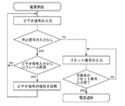
まず、本実施の形態に示す液晶表示装置の駆動方法について、図1に示すフローチャートを参照して説明する。 First, a method for driving the liquid crystal display device described in this embodiment will be described with reference to a flowchart illustrated in FIG.
図1に示すように、本実施の形態に示す液晶表示装置は、電源の供給が開始されると、駆動回路から各画素へビデオ信号を入力していく。入力されるビデオ信号の極性は、mフレーム(mは2以上の自然数)の間保持されている。言い換えると、本実施の形態に示す液晶表示装置では、mフレームごとにビデオ信号の極性が反転される。ここで、mフレーム期間としては、液晶の劣化を抑制するために、例えば1秒程度以下とすることが好ましい。ただし、mフレーム期間はこれに限定されるものではなく、液晶素子に印加する電圧や液晶材料などに合わせて適宜設定すればよい。なお、ビデオ信号の極性は、例えば、対向電極の電位(以下、コモン電位ともよぶ)を基準に決定することができる。 As shown in FIG. 1, the liquid crystal display device described in this embodiment inputs a video signal from a driver circuit to each pixel when power supply is started. The polarity of the input video signal is maintained for m frames (m is a natural number of 2 or more). In other words, in the liquid crystal display device described in this embodiment, the polarity of the video signal is inverted every m frames. Here, the m frame period is preferably set to about 1 second or less, for example, in order to suppress deterioration of the liquid crystal. However, the m frame period is not limited to this, and may be set as appropriate in accordance with a voltage applied to the liquid crystal element, a liquid crystal material, or the like. Note that the polarity of the video signal can be determined based on, for example, the potential of the counter electrode (hereinafter also referred to as a common potential).
次いで、駆動回路から極性の反転されたビデオ信号が各画素へ入力され、mフレーム期間の後に再びビデオ信号の極性が反転されることになる。以下、mフレームごとに極性の反転を行いながら、駆動回路から各画素へ繰り返しビデオ信号が入力されて画像表示が行われる。 Next, a video signal whose polarity is inverted is input to each pixel from the driving circuit, and the polarity of the video signal is inverted again after the m frame period. Thereafter, while the polarity is inverted every m frames, the video signal is repeatedly input from the driving circuit to each pixel, and image display is performed.
従来行われていた1フレーム毎の反転駆動では、画素に印加する電圧レベルが大きい場合に、フレーム間の電圧レベルの大きさが変わらなくても、信号の反転によりビデオ信号の変化量が大きくなり、消費電力が大きくなっていた。これに対して本実施の形態に示す液晶表示装置の駆動方法では、mフレーム期間以上連続して同じ極性のビデオ信号を書き込むことができるので、ビデオ信号の変化量を低減し、低消費電力化を図ることができる。さらに、当該液晶表示装置の駆動方法は、表示する画像が静止画でも動画でも行うことができるので、動画表示時においても消費電力の低減を図ることができる。 In the conventional inversion driving for each frame, when the voltage level applied to the pixel is large, even if the voltage level between frames does not change, the amount of change in the video signal increases due to the inversion of the signal. The power consumption was getting bigger. In contrast, in the driving method of the liquid crystal display device described in this embodiment, video signals having the same polarity can be written continuously for m frame periods or more, so that the amount of change in video signals is reduced and power consumption is reduced. Can be achieved. Furthermore, since the method for driving the liquid crystal display device can be performed on either a still image or a moving image, power consumption can be reduced even when the moving image is displayed.
上記のように駆動回路が各画素へビデオ信号を入力することにより、本実施の形態に示す液晶表示装置は、画像を表示することができる。これに対して、液晶表示装置を非表示状態とする際には、駆動回路に停止信号が入力され、上記のビデオ信号の入力サイクルが終了する。図1に示すように、停止信号が駆動回路に入力されると、駆動回路から各画素へビデオ信号ではなくリセット信号が入力される。全画素にリセット信号が入力されると、液晶表示装置への電源の供給が遮断される。 As described above, when the driver circuit inputs a video signal to each pixel, the liquid crystal display device described in this embodiment can display an image. On the other hand, when the liquid crystal display device is set to the non-display state, a stop signal is input to the drive circuit, and the video signal input cycle is completed. As shown in FIG. 1, when a stop signal is input to the drive circuit, a reset signal is input from the drive circuit to each pixel instead of a video signal. When a reset signal is input to all the pixels, power supply to the liquid crystal display device is cut off.
ここで、停止信号とは、液晶表示装置の画像表示状態を終了させ、画像非表示状態へ移行させる信号である。例えば、リモートコントローラやボタン操作などで直接制御して発信できる信号としても良いし、ビデオ信号の元となるデータ信号などを測定して発信できる信号としても良いし、液晶表示装置に設けられるバックライトの光量などを測定して発信できる信号としても良い。 Here, the stop signal is a signal for ending the image display state of the liquid crystal display device and shifting to the image non-display state. For example, a signal that can be directly controlled by a remote controller or button operation, or a signal that can be transmitted by measuring a data signal that is a source of a video signal, or a backlight provided in a liquid crystal display device can be used. It may be a signal that can be transmitted by measuring the amount of light.
また、リセット信号とは、各画素に入力して液晶の劣化を抑制するための信号である。ここで、液晶素子に正または負のいずれかの極性に保持された電界を長時間にわたって印加し続けると、液晶が劣化し、当該液晶素子の電気特性に異常が生じてしまう。上記のように本実施の形態に示す液晶表示装置の駆動方法では、mフレーム期間以上連続して同じ極性のビデオ信号を書き込むため、従来の1フレームごとにビデオ信号の極性を反転させる駆動方法と比較すると、長時間同じ極性に保持された電界が液晶素子に印加されることになる。 The reset signal is a signal that is input to each pixel to suppress deterioration of the liquid crystal. Here, if an electric field maintained in a positive or negative polarity is continuously applied to the liquid crystal element for a long time, the liquid crystal deteriorates and an abnormality occurs in the electrical characteristics of the liquid crystal element. As described above, in the driving method of the liquid crystal display device described in this embodiment, since video signals having the same polarity are written continuously for m frame periods or more, a conventional driving method for inverting the polarity of a video signal for each frame, In comparison, an electric field held for the same polarity for a long time is applied to the liquid crystal element.
そこで、本実施の形態に示す駆動方法では、停止信号の入力後画素にリセット信号を入力することにより、液晶の劣化の抑制を図っている。リセット信号としては、例えば、正の極性と負の極性で少なくとも1回以上反転させた電位を入力することが好ましい。このとき、正の極性の電位および負の極性の電位の絶対値はできるだけ大きいものとすることが好ましい。なお、リセット信号の極性も、ビデオ信号の極性と同様に、例えば、コモン電位を基準に決定することができる。つまり、リセット信号は、電位がコモン電位より高い期間と、電位がコモン電位より低い期間を少なくとも一回以上繰り返すことになる。 Thus, in the driving method described in this embodiment, deterioration of the liquid crystal is suppressed by inputting a reset signal to the pixel after the stop signal is input. As the reset signal, for example, it is preferable to input a potential that is inverted at least once with a positive polarity and a negative polarity. At this time, the absolute values of the positive polarity potential and the negative polarity potential are preferably as large as possible. Note that the polarity of the reset signal can be determined based on, for example, the common potential, similarly to the polarity of the video signal. That is, the reset signal repeats at least once a period in which the potential is higher than the common potential and a period in which the potential is lower than the common potential.
また、このようにリセット信号として少なくとも1回以上極性を反転させて電位を入力した後、リセット信号の電位をコモン電位と概略等電位とすることが好ましい。さらに、このようにして液晶素子の電極間の電位差を概略0Vとした後、画素に設けられた液晶素子と電気的に接続されたトランジスタをオフ状態とすることが好ましい。 Further, it is preferable that the potential of the reset signal is approximately equal to the common potential after the polarity is inverted at least once as the reset signal and the potential is input. Further, after the potential difference between the electrodes of the liquid crystal element is set to approximately 0 V in this way, it is preferable to turn off the transistor electrically connected to the liquid crystal element provided in the pixel.
また、リセット信号の入力時は、バックライトを非点灯状態としておくことが好ましい。バックライトを非点灯状態としてリセット信号を入力することにより、リセット信号入力に伴う画像の乱れが表示されるのを防ぐことができる。上述のように停止信号をバックライトの点灯と連動させると、バックライト非点灯時にリセット信号の入力を容易に行うことができる。 Further, it is preferable that the backlight be in a non-lighted state when the reset signal is input. By inputting the reset signal while the backlight is in the non-lighting state, it is possible to prevent display of image disturbance due to the input of the reset signal. As described above, when the stop signal is interlocked with the lighting of the backlight, the reset signal can be easily input when the backlight is not lit.
また、図1では液晶表示装置の電源供給の遮断の前にリセット信号を入力しているが、本発明はこれに限られるものではない。液晶表示装置の画素全体が書き換えられるタイミング、例えば、液晶表示装置の画面を暗転させる時などに上記リセット信号を入力することもできる。また、例えば当該液晶表示装置がテレビ受像器として用いられる場合、チャンネルや入力装置の切り替え時、番組がコマーシャルに切り替わる時などに上記リセット信号を入力することもできる。 In FIG. 1, the reset signal is input before the power supply of the liquid crystal display device is cut off, but the present invention is not limited to this. The reset signal can also be input when the entire pixel of the liquid crystal display device is rewritten, for example, when the screen of the liquid crystal display device is darkened. For example, when the liquid crystal display device is used as a television receiver, the reset signal can be input when a channel or an input device is switched or when a program is switched to a commercial.
また、液晶表示装置が画像非表示状態の時に、タイマーで設定した時間に上記リセット信号を入力して液晶の劣化を抑制する構成とすることもできる。液晶表示装置が使用されていない特定の時間(例えば、深夜などのユーザーが通常液晶表示装置を使用しない時間など)に設定してタイマーで液晶表示装置を起動させ、上記リセット信号を入力させればよい。このとき、画像の乱れが表示されるのを防ぐため、バックライトを非点灯状態としておくことが好ましい。 Further, when the liquid crystal display device is in an image non-display state, the reset signal may be input at a time set by a timer to suppress deterioration of the liquid crystal. If you set a specific time when the liquid crystal display device is not used (for example, a time when the user does not normally use the liquid crystal display device such as midnight), start the liquid crystal display device with a timer, and input the reset signal Good. At this time, it is preferable to keep the backlight in a non-lighted state in order to prevent image disturbance from being displayed.
このように、リセット信号の入力を行うことにより、短い時間で極性の反転された電界が液晶素子に少なくとも1回以上印加されるので、上記のようにmフレーム期間以上連続して同じ極性のビデオ信号を書き込んでも、液晶の劣化を抑制することができる。 As described above, by inputting the reset signal, an electric field whose polarity is inverted in a short time is applied to the liquid crystal element at least once. Therefore, as described above, the video having the same polarity is continuously recorded for at least m frame periods. Even when a signal is written, deterioration of the liquid crystal can be suppressed.
以上のようにして、動画表示においても消費電力の低減が図られた液晶表示装置を提供することができる。特に、動画表示においても消費電力の低減が図られた上で、液晶の劣化を抑制することができる液晶表示装置を提供することができる。 As described above, it is possible to provide a liquid crystal display device in which power consumption is reduced even in moving image display. In particular, it is possible to provide a liquid crystal display device capable of suppressing deterioration of liquid crystal while reducing power consumption even in moving image display.
以下に本実施の形態に示す液晶表示装置の構成と駆動方法の一例について、図2乃至図8を用いて示す。 An example of a structure and a driving method of the liquid crystal display device described in this embodiment will be described below with reference to FIGS.
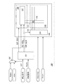
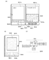
図2に開示する発明の一態様に係る液晶表示装置100のブロック図を示す。液晶表示装置100は、表示制御信号生成回路101と、選択回路102と、表示パネル103と、を有する。
FIG. 3 shows a block diagram of a liquid
表示パネル103は、ゲート線駆動回路104、ソース線駆動回路105および画素部106を有する。画素部106は、複数の画素108を有し、画素108には、少なくとも一対の電極を有する液晶素子が設けられている。ゲート線駆動回路104からゲート線109に供給される走査線信号により、ソース線110に供給されるビデオ信号の画素108への書き込みが制御される。また、ソース線駆動回路105は、デジタル/アナログ変換回路107を有することが好ましい。また、本明細書等において、駆動回路と記載する場合、ゲート線駆動回路104とソース線駆動回路105を含むものとし、さらに、表示制御信号生成回路101、選択回路102なども含める場合がある。
The
表示パネル103には、高電源電位VDDおよび低電源電位VSSによる電源電圧、コモン電位Vcom(共通電位ともいう)が供給される。
The
表示制御信号生成回路101は、外部より入力される同期信号をもとに、ゲート線駆動回路104およびソース線駆動回路105を動作させるための信号を出力する回路である。
The display control
同期信号の一例としては、水平同期信号(Hsync.)、垂直同期信号(Vsync.)、基準クロック信号(CLK)がある。 Examples of the synchronization signal include a horizontal synchronization signal (Hsync.), A vertical synchronization signal (Vsync.), And a reference clock signal (CLK).
ゲート線駆動回路104を動作させるための信号としては、ゲート線側スタートパルスGSP、ゲート線側クロック信号GCLK、等がある。なおゲート線側クロック信号GCLKは、位相をシフトすることで複数のゲート線側クロック信号となったものを含む。
Signals for operating the gate
ソース線駆動回路105を動作させるための信号としては、ソース線側スタートパルスSSP、ソース線側クロック信号SCLK、等がある。なおソース線側クロック信号SCLKは、位相をシフトすることで複数のソース線側クロック信号となったものを含む。
Signals for operating the source
またソース線駆動回路105が有するデジタル/アナログ変換回路107は、外部より入力されるデータ信号data、および表示制御信号生成回路101より入力される極性反転信号POLが供給される。デジタル/アナログ変換回路107は、データ信号dataを極性反転信号POLに基づいて、アナログ値のビデオ信号に変換する。このデータ信号のアナログ値へのビデオ信号の変換は、ラダー抵抗とスイッチを組み合わせた回路で行えばよく、同時にγ補正等を行う構成とすればよい。
The digital /
なおソース線駆動回路105が有するデジタル/アナログ変換回路107は、入力される極性反転信号POLに従って、画素に出力するビデオ信号の極性が切り替え可能な回路であればよく、他の回路とすることも可能である。例えば極性反転信号POLに従って、画素に出力するビデオ信号の極性を切り替える反転アンプを用いてもよい。
Note that the digital /
外部より入力されるデータ信号dataは、デジタルデータである。データ信号dataがアナログデータの場合は、デジタルデータに変換する。 The data signal data input from the outside is digital data. If the data signal data is analog data, it is converted to digital data.
極性反転信号POLは、データ信号dataをアナログ信号であるビデオ信号(Vdataともいう)に変換する際、当該ビデオ信号をコモン電位に対して高い電位(正の極性)または低い電位(負の極性)のいずれかに切り替える信号である。 The polarity inversion signal POL is a high potential (positive polarity) or a low potential (negative polarity) with respect to the common potential when the data signal data is converted into an analog video signal (also referred to as Vdata). It is a signal to switch to either.
ビデオ信号Vdataは、データ信号dataに基づいた電圧である。ビデオ信号Vdataは、ソース線110を介して各画素108の液晶素子の一方の電極に印加される電圧である。液晶素子へのビデオ信号の印加は、画素108へのビデオ信号の書き込みともいう。極性の異なるビデオ信号Vdataであっても、ビデオ信号の電位とコモン電位との差の絶対値が同じであれば、液晶表示装置に入力されるデータ信号dataは同じ値となる。なお、ビデオ信号は、ビデオ信号の電位がコモン電位よりも高い場合、液晶素子に正の極性の電圧が印加されるという。逆に、ビデオ信号の電位がコモン電位よりも低い場合、液晶素子に負の極性の電圧が印加されるという。
The video signal Vdata is a voltage based on the data signal data. The video signal Vdata is a voltage applied to one electrode of the liquid crystal element of each
なお画素に書き込むビデオ信号は、書き込むビデオ信号の電圧レベルから、さらに補正した電圧レベルに変更することで液晶素子の応答を速くすることができる。例えば、ビデオ信号の電圧レベルを、より大きな電圧レベルのビデオ信号に補正しておくことで、液晶素子の応答時間を短くし、素早い画像表示を行うことができる。このような補正信号を加える駆動方法は、オーバードライブ駆動とも呼ばれる。 Note that the response of the liquid crystal element can be accelerated by changing the video signal to be written to the pixel from the voltage level of the video signal to be written to a corrected voltage level. For example, by correcting the voltage level of the video signal to a video signal having a higher voltage level, the response time of the liquid crystal element can be shortened and a quick image display can be performed. Such a driving method for applying a correction signal is also called overdrive driving.
なお、表示制御信号生成回路101において、出力される極性反転信号POLの信号の反転をmフレーム期間毎に行うには、例えば、同期信号である垂直同期信号(Vsync.)の周期をm周期カウントして、極性反転信号POLの信号の反転を行う構成とすればよい。具体的には、垂直同期信号の周期をカウントして得られるカウント値を表示制御信号生成回路101に出力するカウンター回路を設ければよい。カウンター回路が垂直同期信号のカウント値をm周期でリセットし、表示制御信号生成回路101が当該リセットに従って、極性反転信号POLの電位のHレベルとLレベルの切り替えを行う構成とすればよい。
In the display control
また、表示制御信号生成回路101は、液晶表示装置100を非表示状態とする際には、外部より入力される停止信号(STP)に従って、極性反転信号RPOLを出力する。ここで、停止信号STPが表示制御信号生成回路101に入力されると、極性反転信号POLの出力は停止され、その代わりに極性反転信号RPOLが出力される。
The display control
また、選択回路102は、停止信号STPに従って、データ信号dataまたはリセットデータ信号Rdataを選択して、デジタル/アナログ変換回路107に出力する。停止信号STPが入力されていないときは、選択回路102はデータ信号dataを出力し、停止信号STPが入力されると、選択回路102はリセットデータ信号Rdataを出力する。ここで、リセットデータ信号Rdataは、データ信号dataと同様にデジタルデータである。
Further, the
デジタル/アナログ変換回路107に出力されたリセットデータ信号Rdataは、極性反転信号RPOLに従って、アナログ値のリセット信号(Vresとも呼ぶ)に変換される。つまり、極性反転信号RPOLは、リセットデータ信号Rdataをアナログ信号であるリセット信号Vresに変換する際、当該リセット信号をコモン電位に対して高い電位(正の極性)または低い電位(負の極性)のいずれかに切り替える信号である。
The reset data signal Rdata output to the digital /
画像表示時には、垂直同期信号(Vsync.)に応じて表示制御信号生成回路101から極性反転信号POLが出力され、選択回路102から出力されたデータ信号dataをデジタル/アナログ変換回路107で極性反転信号POLに応じてビデオ信号Vdataに変化する。これに対して、画像を非表示とする際には、停止信号STPに応じて表示制御信号生成回路101から極性反転信号RPOLが出力され、選択回路102から出力されたリセットデータ信号Rdataをデジタル/アナログ変換回路107で極性反転信号RPOLに応じてリセット信号Vresに変化する。
At the time of image display, the polarity inversion signal POL is output from the display control
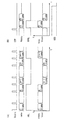
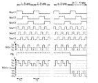
図3(A)は、液晶表示装置100の画像表示時における、表示制御信号生成回路101、選択回路102、および表示パネル103に入出力される信号を模式的に示したタイミングチャート図である。
FIG. 3A is a timing chart schematically showing signals input to and output from the display control
図3(A)に示すタイミングチャート図では、垂直同期信号(Vsync.)、データ信号(data)、極性反転信号POLの波形を模式的に示している。また、図3(A)に示すタイミングチャート図では、横軸を時間、縦軸を画素の液晶素子に印加するビデオ信号Vdataの電圧レベルとして示している。 In the timing chart shown in FIG. 3A, waveforms of the vertical synchronization signal (Vsync.), The data signal (data), and the polarity inversion signal POL are schematically shown. In the timing chart shown in FIG. 3A, the horizontal axis represents time, and the vertical axis represents the voltage level of the video signal Vdata applied to the liquid crystal element of the pixel.
図3(A)に示すタイミングチャート図では、垂直同期信号のHレベルの周期に同期して、データ信号が1フレーム目乃至m(mは2以上の自然数)フレーム目で連続して供給されている。極性反転信号POLは、垂直同期信号のHレベルをカウントしてm回ごとに信号の反転を行う。そして極性反転信号POLをmフレーム毎に反転した信号とすることができる。 In the timing chart shown in FIG. 3A, the data signal is continuously supplied from the first frame to m (m is a natural number of 2 or more) frames in synchronization with the H level cycle of the vertical synchronization signal. Yes. The polarity inversion signal POL counts the H level of the vertical synchronization signal and inverts the signal every m times. The polarity inversion signal POL can be a signal obtained by inverting every m frames.
極性反転信号POLの反転に従って正の極性または負の極性に反転されたビデオ信号は、コモン電位に対する電圧レベルとして、各画素に書き込まれる。図3(A)に示すように、本実施の形態の構成では、mフレーム期間連続して、同じ極性の反転状態を保持して動作をさせることができる。 The video signal inverted to the positive polarity or the negative polarity in accordance with the inversion of the polarity inversion signal POL is written to each pixel as a voltage level with respect to the common potential. As shown in FIG. 3A, in the configuration of this embodiment, the operation can be performed while maintaining the inverted state of the same polarity for m frame periods continuously.
通常、表示素子に液晶素子を用いる表示装置では、ゲートライン反転駆動、ソースライン反転駆動、フレーム反転駆動、ドット反転駆動といった、1フレーム期間毎に正負の極性を交互に表示素子に与える反転駆動を行っている。しかしながら、液晶素子に印加するビデオ信号の電圧レベルが大きい場合に反転駆動を行うと、表示素子に印加する電圧レベルの大きさが変わらなくても、信号の反転によりビデオ信号の変化量が大きくなり、消費電力が大きくなる。消費電力の増大は、駆動周波数の大きい駆動の場合に特に顕著になる。 Usually, in a display device using a liquid crystal element as a display element, inversion driving that alternately gives positive and negative polarities to the display element every frame period, such as gate line inversion driving, source line inversion driving, frame inversion driving, and dot inversion driving. Is going. However, if the inversion drive is performed when the voltage level of the video signal applied to the liquid crystal element is large, even if the voltage level applied to the display element does not change, the amount of change in the video signal increases due to the inversion of the signal. , Power consumption increases. The increase in power consumption becomes particularly significant when driving with a high driving frequency.
一方で図3(A)に示す例では、mフレーム期間以上連続して、同じ極性のビデオ信号の印加により書き込みをすることができる。そのため、1フレーム期間毎に反転駆動を行っていた場合に、反転駆動に伴うビデオ信号の変化量が大きくなっていた問題を低減することができ、低消費電力化を図ることができる。 On the other hand, in the example shown in FIG. 3A, writing can be performed by applying a video signal having the same polarity for m frame periods or more. Therefore, when the inversion drive is performed for each frame period, the problem that the amount of change in the video signal due to the inversion drive is large can be reduced, and the power consumption can be reduced.
なお、図3(A)に示したように本実施の形態で示す構成では、mフレーム期間毎に反転駆動している。そのためmフレーム目から(m+1)フレーム目、および2mフレーム目から(2m+1)フレーム目では、ビデオ信号の変化が大きくなってしまう。これに対して、mフレーム目から(m+1)フレーム目、および2mフレーム目から(2m+1)フレーム目では、ビデオ信号をコモン電位Vcomと概略等電位とするブランク期間を設ける構成とすることにより、ビデオ信号の変化を小さくすることができる。これによりさらなる消費電力の低減を図ることができる。 Note that in the structure shown in this embodiment mode as shown in FIG. 3A, inversion driving is performed every m frame periods. Therefore, the video signal changes greatly from the mth frame to the (m + 1) th frame and from the 2mth frame to the (2m + 1) th frame. On the other hand, in the m-th frame to the (m + 1) -th frame and the 2m-th frame to the (2m + 1) -th frame, a blank period in which the video signal is approximately equal to the common potential Vcom is provided. The change in signal can be reduced. As a result, the power consumption can be further reduced.
また、図3(B)は、液晶表示装置100の画像を非表示にする際の、表示制御信号生成回路101、選択回路102、および表示パネル103に入出力される信号を模式的に示したタイミングチャート図である。
FIG. 3B schematically shows signals input to and output from the display control
図3(B)に示すタイミングチャート図では、停止信号(STP)、リセットデータ信号(Rdata)、極性反転信号RPOLの波形を模式的に示している。また、図3(B)に示すタイミングチャート図では、横軸を時間、縦軸を画素の液晶素子に印加するリセット信号Vresの電圧レベルとして示している。 In the timing chart shown in FIG. 3B, waveforms of the stop signal (STP), the reset data signal (Rdata), and the polarity inversion signal RPOL are schematically shown. In the timing chart shown in FIG. 3B, the horizontal axis represents time, and the vertical axis represents the voltage level of the reset signal Vres applied to the liquid crystal element of the pixel.
図3(B)に示すタイミングチャート図では、停止信号STPのHレベルが入力されると、リセットデータ信号がR1フレーム目およびR2フレーム目に入力される。ここでR1フレーム目は停止信号STPが入力されてから1フレーム目を指し、R2フレーム目は停止信号STPが入力されてから2フレーム目を指す。極性反転信号RPOLは、R1フレーム目とR2フレーム目で反転しており、図3(B)では、極性反転信号RPOLは、R1フレーム目で正の極性、R2フレーム目で負の極性となる。 In the timing chart shown in FIG. 3B, when the H level of the stop signal STP is input, the reset data signal is input to the R1 frame and the R2 frame. Here, the R1 frame indicates the first frame after the stop signal STP is input, and the R2 frame indicates the second frame after the stop signal STP is input. The polarity inversion signal RPOL is inverted in the R1 and R2 frames. In FIG. 3B, the polarity inversion signal RPOL has a positive polarity in the R1 frame and a negative polarity in the R2 frame.
極性反転信号RPOLに従って正の極性または負の極性に反転されたリセット信号Vresは、コモン電位Vcomに対する電圧レベルとして、各画素に書き込まれる。図3(B)では、リセット信号Vresは、R1フレーム目で正の極性、R2フレーム目で負の極性となる。このとき、電圧レベルの絶対値はできるだけ大きく、例えば、ビデオ信号の電圧レベルの絶対値の最大値と同程度にすることが好ましい。また、R1フレーム目のリセット信号Vresの極性は、停止信号STPが入力されたときのビデオ信号Vdataの極性に対して、反転させた極性とすることが好ましい。このようにリセット信号Vresをすべての画素に入力した後、高電源電位VDDの供給を遮断すればよい。 The reset signal Vres inverted to a positive polarity or a negative polarity according to the polarity inversion signal RPOL is written to each pixel as a voltage level with respect to the common potential Vcom. In FIG. 3B, the reset signal Vres has a positive polarity in the R1 frame and a negative polarity in the R2 frame. At this time, the absolute value of the voltage level is as large as possible, and is preferably about the same as the maximum absolute value of the voltage level of the video signal, for example. Further, it is preferable that the polarity of the reset signal Vres of the R1 frame is reversed with respect to the polarity of the video signal Vdata when the stop signal STP is input. In this way, after the reset signal Vres is input to all the pixels, the supply of the high power supply potential VDD may be cut off.
このように、リセット信号Vresの入力を行うことにより、上記のようにmフレーム期間以上連続して同じ極性のビデオ信号を書き込んでも、液晶の劣化を抑制することができる。従って、動画表示においても消費電力の低減が図られた上で、液晶の劣化を抑制することができる液晶表示装置を提供することができる。 In this manner, by inputting the reset signal Vres, it is possible to suppress deterioration of the liquid crystal even when video signals having the same polarity are written continuously for m frame periods or more as described above. Therefore, it is possible to provide a liquid crystal display device that can suppress deterioration of liquid crystal while reducing power consumption even in moving image display.
なお、図3(B)では、リセット信号を、R1フレーム目とR2フレーム目の2フレームで正の極性と負の極性の電位をそれぞれ印加しているが、これに限られることなく、3フレーム以上、電位の極性を反転させながら、リセット信号を入力させる構成としても良い。また、停止信号STPが入力されたときのビデオ信号Vdataの電位の極性と反転させた極性の電位のリセット信号を1フレーム分だけ入力させる構成とすることも可能である。 In FIG. 3B, the reset signal is applied with a positive polarity potential and a negative polarity potential in two frames of the R1 frame and the R2 frame, but the present invention is not limited to this. As described above, the reset signal may be input while inverting the polarity of the potential. It is also possible to input a reset signal having a potential of the polarity reversed from the polarity of the potential of the video signal Vdata when the stop signal STP is input for one frame.
また、図3(B)において、R1フレーム目、R2フレーム目の長さは、図3(A)に示す1フレーム期間と同等であるが、本実施の形態に示す液晶表示装置はこれに限られるものではなく、R1フレーム目、R2フレーム目またはR3フレーム目以降の長さを1フレーム期間以上としてもよい。 In FIG. 3B, the lengths of the R1 frame and the R2 frame are equivalent to the one frame period shown in FIG. 3A. However, the liquid crystal display device described in this embodiment is not limited to this. The length after the R1 frame, the R2 frame, or the R3 frame may be one frame period or longer.
また、このようにリセット信号Vresとして少なくとも1回以上極性を反転させて電位を入力した後、リセット信号Vresの電位をコモン電位Vcomと概略等電位とすることが好ましい。例えば、図3(B)において、R2フレーム目の次にリセット信号の電圧レベルがコモン電位VcomとなるR3フレーム目を設ける構成とすればよい。さらに、このようにして液晶素子の電極間の電位差を概略0Vとした後、画素に設けられた液晶素子と電気的に接続されたトランジスタをオフ状態とすることが好ましい。 Further, it is preferable that the potential of the reset signal Vres is approximately equal to the common potential Vcom after the polarity is inverted at least once as the reset signal Vres and the potential is input. For example, in FIG. 3B, a configuration may be employed in which an R3 frame in which the voltage level of the reset signal becomes the common potential Vcom is provided after the R2 frame. Further, after the potential difference between the electrodes of the liquid crystal element is set to approximately 0 V in this way, it is preferable to turn off the transistor electrically connected to the liquid crystal element provided in the pixel.
次いで、図2で示した表示パネル103の構成について、具体的な構成例を示し、本実施の形態の効果について詳述する。
Next, a specific configuration example of the configuration of the
図4は、図2で示した表示パネル103が有するゲート線駆動回路104、ソース線駆動回路105および画素部106の構成を具体的に示したものである。
FIG. 4 specifically shows the configuration of the gate
ゲート線駆動回路104は、シフトレジスタ回路201を有する。ソース線駆動回路105は、シフトレジスタ回路202、デジタル/アナログ変換回路107およびアナログスイッチ203を有する。
The gate
図4で画素部106は、3行3列の画素108を有する構成を一例として示している。画素108は、それぞれトランジスタ204、容量素子205、および液晶素子206を有する。トランジスタ204は、ゲートがゲート線109に接続され、ソースまたはドレインの一方がソース線110に接続されている。
In FIG. 4, the
トランジスタ204としては、オフ状態における電流(オフ電流)が低いトランジスタを用いることが好ましく、例えば、酸化物半導体を用いたトランジスタを用いることが好ましい。このようなトランジスタをトランジスタ204として用いることにより、容量素子205および液晶素子206からトランジスタ204を介して電荷が漏れにくくなるので、液晶素子206に加える電圧を長時間保持することができる。これにより、液晶表示装置100の表示画像の保持特性を高くすることができる。
As the
一方、このようにトランジスタ204としてオフ電流の低いトランジスタを用いると、液晶表示装置100の電源をオフ状態とした後も、トランジスタ204と接続される液晶素子206の電圧が保持されてしまい、極性が保持された電界が液晶に長時間印加されて液晶が劣化するおそれがある。これに対して上述のように、リセット信号の入力の際に、少なくとも1回以上極性を反転させて電位を入力した後、リセット信号Vresの電位をコモン電位Vcomと概略等電位にしてトランジスタ204をオフ状態とすることにより、極性が保持された電界が液晶に長時間印加されるのを抑制することができる。
On the other hand, when a transistor with a low off-state current is used as the
また、上述のように液晶表示装置100の電源がオフ状態の時に、タイマーで設定した時間に液晶表示装置100を起動させて、上記リセット信号を入力する構成とすることが好ましい。これにより、液晶表示装置100の電源をオフ状態としたときに液晶素子206の電圧が保持されていてもタイマーで設定した時刻に液晶の状態を電界がかかっていない状態にすることができる。
Further, it is preferable that the liquid
図4において、ゲート線駆動回路104が有するシフトレジスタ回路201は、ゲート線側スタートパルスGSP、ゲート線側クロック信号GCLKが入力される。シフトレジスタ回路201は、1〜3行目にあるゲート線109に対して選択信号Gout1〜Gout3により順番にHレベルの信号を出力して、トランジスタ204の導通状態を制御することができる。
In FIG. 4, the
図4において、ソース線駆動回路105が有するデジタル/アナログ変換回路107は、画像表示時には、データ信号data、および極性反転信号POLに応じて生成されるビデオ信号Vdataを出力する。また、画像を非表示状態にする際には、リセットデータ信号Rdata、および極性反転信号RPOLに応じて生成されるリセット信号Vresを出力する。ビデオ信号Vdataおよびリセット信号Vresは、アナログスイッチ203が導通状態となることで、ソース線110を介して画素108の容量素子205および液晶素子206に書き込まれる。
In FIG. 4, a digital /
図4において、ソース線駆動回路105が有するシフトレジスタ回路202は、ソース線側スタートパルスSSP、ソース線側クロック信号SCLKが入力される。シフトレジスタ回路202は、1〜3列目にあるアナログスイッチ203に対して選択信号Sout1〜Sout3により順番にHレベルの信号を出力し、アナログスイッチ203の導通状態を制御することができる。
In FIG. 4, the
次いで図5(A)に示した画素部の模式図および図5(B)に示したデータ信号に基づく正または負の極性によるビデオ信号をもとにして、複数のフレーム期間にわたる本発明の駆動方法の具体的な動作の一例について説明する。 Next, based on the schematic diagram of the pixel portion shown in FIG. 5A and the video signal with the positive or negative polarity based on the data signal shown in FIG. An example of a specific operation of the method will be described.
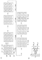
図5(A)に示す図は、画像表示時の1フレーム目、2フレーム目、mフレーム目および(m+1)フレーム目、画像を非表示にする時のR1フレーム目、R2フレーム目およびR3フレーム目に、3行3列の画素部に入力されるデータ信号の模式図である。ここで、R1フレーム目は停止信号STPが入力されてから1フレーム目を指し、R2フレーム目は2フレーム目を、R3フレームは3フレーム目を指す。 FIG. 5A shows the first frame, the second frame, the m-th frame and the (m + 1) -th frame when displaying an image, and the R1-, R2- and R3-frames when the image is not displayed. FIG. 3 is a schematic diagram of a data signal input to a pixel portion of 3 rows and 3 columns. Here, the R1 frame indicates the first frame after the stop signal STP is input, the R2 frame indicates the second frame, and the R3 frame indicates the third frame.
図5(A)の1フレーム目では、1行1列目の画素211、2行1列目の画素221および3行1列目の画素231にはデータ信号として”VA”を、1行2列目の画素212、2行2列目の画素222および3行2列目の画素232にはデータ信号として”VB”を、1行3列目の画素213、2行3列目の画素223および3行3列目の画素233にはデータ信号として”VC”を入力する例を示している。
In the first frame of FIG. 5A, the
また図5(A)で示したデータ信号”VA”、”VB”および”VC”を、ビデオ信号の電圧レベルの大きさとすると、|VA|、|VB|、|VC|と表すことができる。また説明のため、|VA|、|VB|、|VC|の大小関係を一例として表すと、|VC|<|VB|<|VA|となる。極性反転信号POLがHレベル(POL_H)の場合、図5(B)に示すようにビデオ信号は、”VA”、”VB”および”VC”として表記でき、正の極性のビデオ信号を書き込むとして説明をすることができる。また、極性反転信号POLがLレベル(POL_L)の場合、図5(B)に示すようにビデオ信号は、”−VA”、”−VB”および”−VC”として表記でき、負の極性のビデオ信号を書き込むとして説明をすることができる。なお図5(B)に示すように、”VA”、”VB”および”VC”と、”−VA”、”−VB”および”−VC”とのビデオ信号は、コモン電位Vcomを挟んで対称となる同じ大きさである。 If the data signals “V A ”, “V B ”, and “V C ” shown in FIG. 5A are the magnitudes of the voltage levels of the video signal, | V A |, | V B |, | V C | For the sake of explanation, if the magnitude relation of | V A |, | V B |, | V C | is expressed as an example, | V C | <| V B | <| V A | When the polarity inversion signal POL is at H level (POL_H), the video signal can be expressed as “V A ”, “V B ”, and “V C ” as shown in FIG. Can be described as writing. When the polarity inversion signal POL is L level (POL_L), the video signal can be expressed as “−V A ”, “−V B ” and “−V C ” as shown in FIG. It can be described as writing a video signal of the polarity. As shown in FIG. 5B, the video signals “V A ”, “V B ” and “V C ” and “−V A ”, “−V B ” and “−V C ” It is the same size that is symmetrical across the common potential Vcom.
また、図5(A)において、2フレーム目では、画素211、画素221および画素231に”VB”を、画素212、画素222および画素232に”VC”を、画素213、画素223および画素233に”VA”をデータ信号として入力している。
Further, in FIG. 5 (A), the in the second frame, the "V B" to
また、図5(A)において、mフレーム目では、画素211、画素221および画素231に”VC”を、画素212、画素222および画素232に”VA”を、画素213、画素223および画素233に”VB”をデータ信号として入力している。
Further, in FIG. 5 (A), the in m th frame, the "V C" to
また、図5(A)において、(m+1)フレーム目では、画素211、画素221および画素231に”VB”を、画素212、画素222および画素232に”VC”を、画素213、画素223および画素233に”VA”をデータ信号として入力している。
Further, in FIG. 5 (A), (m + 1) in the frame, the
また、図5(A)において、R1フレーム目では、すべての画素に”VA”をデータ信号として入力しており、R2フレーム目でも同様に、すべての画素に”VA”をデータ信号として入力している。また、図5(A)において、R3フレーム目では、すべての画素にコモン電位Vcomに対応する”Vcom”をデータ信号として入力している。 Further, in FIG. 5 (A), the in R1-th frame, and enter all the "V A" to pixel as a data signal, also in R2-th frame, the "V A" to all the pixels as a data signal You are typing. In FIG. 5A, in the R3 frame, “V com ” corresponding to the common potential Vcom is input as a data signal to all the pixels.
図6は、図5(A)で示した画像表示時の画素部へのデータ信号の入力をもとにしたタイミングチャート図である。図6に示すタイミングチャート図では、1フレーム目、2フレーム目、mフレーム目および(m+1)フレーム目における、選択信号Gout1〜Gout3、選択信号Sout1〜Sout3、データ信号data、極性反転信号POL、およびビデオ信号Vdataを示している。なお図6に示すタイミングチャート図では、点順次駆動として説明を行うが、線順次駆動とする構成であってもよい。 FIG. 6 is a timing chart based on the input of a data signal to the pixel portion at the time of image display shown in FIG. In the timing chart shown in FIG. 6, the selection signals Gout1 to Gout3, the selection signals Sout1 to Sout3, the data signal data, the polarity inversion signal POL, and the first frame, the second frame, the mth frame, and the (m + 1) th frame. A video signal Vdata is shown. Note that the timing chart shown in FIG. 6 is described as dot-sequential driving, but may be configured to be line-sequential driving.
図6に示すタイミングチャート図では、図3(A)で説明したように、極性反転信号POLの信号の反転をmフレーム期間毎に行う構成とすることができる。そのため、本実施の形態におけるビデオ信号Vdataを、mフレーム期間連続して、同じ極性のビデオ信号として動作させることができる。そのため、1フレーム期間毎に反転駆動を行っていた場合に、反転駆動に伴うビデオ信号の変化量が大きくなっていた問題を低減することができ、低消費電力化を図ることができる。 In the timing chart shown in FIG. 6, as described in FIG. 3A, the polarity inversion signal POL can be inverted every m frame periods. Therefore, the video signal Vdata in this embodiment can be operated as a video signal having the same polarity for m frame periods continuously. Therefore, when the inversion drive is performed for each frame period, the problem that the amount of change in the video signal due to the inversion drive is large can be reduced, and the power consumption can be reduced.
次いで図7では、図6で示したタイミングチャート図において、画素部における1列目のビデオ信号の変化について抜き出して説明する。 Next, in FIG. 7, a change in the video signal in the first column in the pixel portion in the timing chart shown in FIG. 6 is extracted and described.
図7(A)に示す図は、図6における期間T1およびT2でのビデオ信号の変化について抜き出して示した模式図である。また図7(B)に示す図は、図6に示すタイミングチャートに対して1フレーム毎に極性反転信号POLを反転させる構成とした場合の、図6における期間T1およびT2に対応する期間T1RおよびT2Rでのビデオ信号の変化について抜き出して示した模式図である。つまり、図7(B)においては、期間T1Rと期間T2Rでビデオ信号の極性が反転されている。 The diagram shown in FIG. 7A is a schematic diagram showing extracted video signals in the periods T1 and T2 in FIG. 7B shows a period T1R corresponding to the periods T1 and T2 in FIG. 6 when the polarity inversion signal POL is inverted every frame with respect to the timing chart shown in FIG. It is the schematic diagram which extracted and showed about the change of the video signal in T2R. That is, in FIG. 7B, the polarity of the video signal is inverted between the period T1R and the period T2R.
図7(A)に示す期間T1は、1フレーム目の1行目の各列におけるビデオ信号を表すものである。また図7(A)に示す期間T2は、2フレーム目の1行目の各列におけるビデオ信号を表すものである。また図7(B)に示す期間T1Rは、1フレーム目の1行目の各列におけるビデオ信号を表すものである。また図7(B)に示す期間T2Rは、2フレーム目の1行目の各列におけるビデオ信号を表すものである。なお図7(A)および図7(B)では、期間T1と期間T2と、期間T1Rと期間T2Rとの、同じ列でのビデオ信号に着目し、両者の変化について矢印で指し示している。 A period T1 shown in FIG. 7A represents a video signal in each column of the first row of the first frame. A period T2 shown in FIG. 7A represents a video signal in each column of the first row of the second frame. A period T1R shown in FIG. 7B represents a video signal in each column of the first row of the first frame. A period T2R shown in FIG. 7B represents a video signal in each column of the first row of the second frame. Note that in FIGS. 7A and 7B, attention is paid to video signals in the same column of the period T1 and the period T2, and the period T1R and the period T2R, and changes in both are indicated by arrows.
図7(A)における、1行の各列の1フレーム目と2フレーム目との間におけるビデオ信号の差を列挙すると、1列目では|VA−VB|であり、2列目では|VB−VC|であり、3列目では|VC−VA|である。また、図7(B)における、1行の各列の1フレーム目と2フレーム目との間におけるビデオ信号の差を列挙すると、1列目では|VA+VB|であり、2列目では|VB+VC|であり、3列目では|VC+VA|である。 In FIG. 7A, differences in video signals between the first frame and the second frame of each column in one row are listed. In the first column, | V A −V B | | V B −V C | and | V C −V A | in the third column. In addition, when differences in video signals between the first frame and the second frame of each column in one row in FIG. 7B are listed, | V A + V B | Is | V B + V C |, and in the third column is | V C + V A |.
図7(A)と図7(B)とで、同じ列でのビデオ信号に着目すると、電圧の変化が大きいのは、図7(B)に示した1フレーム毎に極性反転信号POLを反転させて、フレーム反転駆動とした場合である。一方で図7(A)に示した極性反転信号POLの信号の反転をmフレーム期間毎に行う構成とした場合は、同じ列でのビデオ信号の変化が小さい。従って図7(A)の場合、画素に書き込むビデオ信号の充放電に要する消費電力を小さくすることができる。 In FIGS. 7A and 7B, focusing on video signals in the same column, the change in voltage is large because the polarity inversion signal POL is inverted for each frame shown in FIG. 7B. In this case, the frame inversion drive is used. On the other hand, when the polarity inversion signal POL shown in FIG. 7A is inverted every m frame periods, the change in the video signal in the same column is small. Accordingly, in the case of FIG. 7A, power consumption required for charging and discharging a video signal written to a pixel can be reduced.
従って、動画表示においても消費電力の低減が図られた液晶表示装置を提供することができる。 Accordingly, it is possible to provide a liquid crystal display device in which power consumption is reduced even in moving image display.
図8は、図5(A)で示した画像を非表示にする際の画素部へのデータ信号の入力をもとにしたタイミングチャート図である。図8に示すタイミングチャート図では、R1フレーム目、R2フレーム目およびR3フレーム目における、選択信号Gout1〜Gout3、選択信号Sout1〜Sout3、リセットデータ信号Rdata、極性反転信号RPOL、およびリセット信号Vresを示している。なお図8に示すタイミングチャート図においても、点順次駆動として説明を行うが、線順次駆動とする構成であってもよい。 FIG. 8 is a timing chart based on the input of a data signal to the pixel portion when the image shown in FIG. 5A is not displayed. In the timing chart shown in FIG. 8, the selection signals Gout1 to Gout3, the selection signals Sout1 to Sout3, the reset data signal Rdata, the polarity inversion signal RPOL, and the reset signal Vres are shown in the R1, R2, and R3 frames. ing. Note that the timing chart shown in FIG. 8 is also described as point-sequential driving, but may be configured to be line-sequential driving.
図8に示すタイミングチャート図では、図3(B)で説明したように、極性反転信号RPOLの電位の反転をR1フレーム目とR2フレーム目の間で行う。これにより、R1フレーム目では、リセット信号Vresとして電位VAが入力され、R2フレーム目ではリセット信号Vresとして電位−VAが入力される。このように、リセット信号Vresの入力を行うことにより、図6に示すようにmフレーム期間以上連続して同じ極性のビデオ信号を書き込んでも、液晶の劣化を抑制することができる。また、リセット信号Vresの電位を、このようにビデオ信号Vdataの電圧レベルの絶対値の最大値と同程度にすることにより、強い電界を反転して液晶素子に印加することができるので、より液晶素子の劣化を抑制することができる。 In the timing chart shown in FIG. 8, as described in FIG. 3B, the potential of the polarity inversion signal RPOL is inverted between the R1 frame and the R2 frame. Thus, the R1-th frame, the potential V A is input as a reset signal Vres, the R2-th frame potential -V A is input as a reset signal Vres. In this manner, by inputting the reset signal Vres, it is possible to suppress deterioration of the liquid crystal even when video signals having the same polarity are written continuously for m frame periods or more as shown in FIG. In addition, by setting the potential of the reset signal Vres to be approximately the same as the maximum absolute value of the voltage level of the video signal Vdata, a strong electric field can be inverted and applied to the liquid crystal element. Deterioration of the element can be suppressed.
また、R3フレーム目でリセット信号Vresとして、”Vcom”のデータ信号に対応するコモン電位Vcomを入力する。このようにして液晶素子の電極間の電位差を概略0Vとした後、画素に設けられた液晶素子206と電気的に接続されたトランジスタ204をオフ状態とすることにより、極性が保持された電界が液晶に長時間印加されるのを抑制することができる。
In addition, the common potential Vcom corresponding to the data signal “V com ” is input as the reset signal Vres in the R3th frame. After the potential difference between the electrodes of the liquid crystal element is set to approximately 0 V in this manner, the
以上のようにして、動画表示においても消費電力の低減が図られた上で、液晶の劣化を抑制することができる液晶表示装置を提供することができる。 As described above, it is possible to provide a liquid crystal display device capable of suppressing deterioration of liquid crystal while reducing power consumption even in moving image display.
また本実施の形態では、フレーム反転駆動を行う液晶表示装置を例に挙げて説明したが、他の構成としてもよい。例えば、ゲートライン反転駆動、ソースライン反転駆動またはドット反転駆動などを行う液晶表示装置としてもよい。 In this embodiment, the liquid crystal display device that performs frame inversion driving is described as an example. However, other configurations may be used. For example, a liquid crystal display device that performs gate line inversion driving, source line inversion driving, or dot inversion driving may be used.
以上、本実施の形態に示す構成、方法などは、他の実施の形態に示す構成、方法などと適宜組み合わせて用いることができる。 The structures, methods, and the like described in this embodiment can be combined as appropriate with any of the structures, methods, and the like described in the other embodiments.
(実施の形態2)
本実施の形態では、表示装置の外観及び断面等を示し、その構成について説明する。本実施の形態では、表示素子として液晶素子を用いた例をあげて説明する。
(Embodiment 2)
In this embodiment mode, an appearance, a cross section, and the like of a display device are shown and the structure thereof will be described. In this embodiment, an example in which a liquid crystal element is used as a display element will be described.
なお液晶表示装置とは、コネクター、例えばFPC(Flexible printed circuit)もしくはTCP(Tape Carrier Package)が取り付けられたモジュール、TCPの先にプリント配線板が設けられたモジュール、または表示素子にCOG(Chip On Glass)方式によりIC(集積回路)が直接実装されたモジュールも全て液晶表示装置に含むものとする。 Note that a liquid crystal display device is a connector, for example, a module in which an FPC (Flexible Printed Circuit) or TCP (Tape Carrier Package) is attached, a module in which a printed wiring board is provided at the end of TCP, or a COG (Chip On) in a display element. All modules on which an IC (integrated circuit) is directly mounted by the Glass method are also included in the liquid crystal display device.
液晶表示装置の外観及び断面について、図9(A1)(A2)(B)を用いて説明する。図9(A1)(A2)は、トランジスタ4010、4011、及び液晶素子4013を、第1の基板4001と第2の基板4006との間にシール材4005によって封止した、パネルの平面図であり、図9(B)は、図9(A1)(A2)のM−Nにおける断面図に相当する。
The appearance and cross section of the liquid crystal display device will be described with reference to FIGS. 9A1, 9A2, and 9B. 9A1 and 9A2 are plan views of a panel in which the
第1の基板4001上に設けられた画素部4002と、ゲート線駆動回路4004とを囲むようにして、シール材4005が設けられている。また画素部4002と、ゲート線駆動回路4004の上に第2の基板4006が設けられている。よって画素部4002と、ゲート線駆動回路4004とは、第1の基板4001とシール材4005と第2の基板4006とによって、液晶層4008と共に封止されている。また第1の基板4001上のシール材4005によって囲まれている領域とは異なる領域に、別途用意された基板上に単結晶半導体膜又は多結晶半導体膜で形成されたソース線駆動回路4003が実装されている。
A
また、図9では図示しないが、光源として画素に光を照射するバックライトを適宜設けることができる。ここで、バックライトは、上記リセット信号の入力時に非点灯状態とすることが好ましい。これにより、リセット信号入力に伴う画像の乱れが表示されるのを防ぐことができる。また、図9では図示しないが、設定した時間に前記液晶表示装置を起動させるタイマーを適宜設けることができる。ここで、当該タイマーは、液晶表示装置が使用されていない特定の時間(例えば、深夜などのユーザーが通常液晶表示装置を使用しない時間など)に設定して液晶表示装置を起動させ、上記リセット信号を入力させればよい。また、位相差板、反射防止膜などの光学フィルムなどは適宜設けることができる。また、カラーフィルタ層として機能する着色層を設けることができる。 Although not illustrated in FIG. 9, a backlight that irradiates light to pixels can be provided as appropriate as a light source. Here, the backlight is preferably in a non-lighting state when the reset signal is input. As a result, it is possible to prevent the display of image disturbance accompanying the reset signal input. Further, although not shown in FIG. 9, a timer for starting the liquid crystal display device at a set time can be provided as appropriate. Here, the timer is set to a specific time when the liquid crystal display device is not used (for example, a time when the user does not normally use the liquid crystal display device such as midnight) and starts the liquid crystal display device, and the reset signal Can be entered. In addition, an optical film such as a retardation plate or an antireflection film can be provided as appropriate. In addition, a colored layer functioning as a color filter layer can be provided.
なお、別途形成した駆動回路の接続方式は、特に限定されるものではなく、COG方式、ワイヤボンディング方式、或いはTAB方式などを用いることができる。図9(A1)は、COG方式によりソース線駆動回路4003を実装する例であり、図9(A2)は、TAB方式によりソース線駆動回路4003を実装する例である。
Note that a connection method of a driver circuit which is separately formed is not particularly limited, and a COG method, a wire bonding method, a TAB method, or the like can be used. FIG. 9A1 illustrates an example in which the source
また第1の基板4001上に設けられた画素部4002と、ゲート線駆動回路4004は、トランジスタを複数有しており、図9(B)では、画素部4002に含まれるトランジスタ4010と、ゲート線駆動回路4004に含まれるトランジスタ4011とを例示している。トランジスタ4010、4011上には絶縁層4020、4021が設けられている。
In addition, the
トランジスタ4010、4011は、非晶質、微結晶、多結晶または単結晶である、シリコン又はゲルマニウムなどの薄膜の半導体を半導体層に適用することができる。或いは、トランジスタ4010、4011は、酸化物半導体を半導体層に適用することができる。本実施の形態において、トランジスタ4010、4011はnチャネル型トランジスタである。酸化物半導体を半導体層に適用することで、オフ電流の極めて低いトランジスタを画素のスイッチング素子に用いることができる。この場合、一度画素に書き込んだビデオ電圧の変動が小さいため、表示品位の向上を図ることができる。
As the
ここで、電子供与体(ドナー)となる水分または水素などの不純物が低減され、なおかつ酸素欠損が低減されることにより高純度化された酸化物半導体(purified OS)は、i型(真性半導体)又はi型に限りなく近い。そのため、高純度化された酸化物半導体を半導体層に有するトランジスタは、オフ電流が極めて小さく、信頼性が高い。 Here, an oxide semiconductor (purified OS) that is highly purified by reducing impurities such as moisture or hydrogen serving as an electron donor (donor) and reducing oxygen vacancies is an i-type (intrinsic semiconductor). Or it is close to i type. Therefore, a transistor including a highly purified oxide semiconductor in a semiconductor layer has extremely low off-state current and high reliability.
具体的に、高純度化された酸化物半導体膜にチャネル形成領域を有するトランジスタのオフ電流が小さいことは、いろいろな実験により証明できる。例えば、チャネル幅が1×106μmでチャネル長が10μmの素子であっても、ソース電極とドレイン電極間の電圧(ドレイン電圧)が1Vから10Vの範囲において、オフ電流が、半導体パラメータアナライザの測定限界以下、すなわち1×10⁻¹³A以下という特性を得ることができる。この場合、オフ電流をトランジスタのチャネル幅で規格化したオフ電流は、100zA/μm以下であることが分かる。また、容量素子とトランジスタとを接続して、容量素子に流入または容量素子から流出する電荷を当該トランジスタで制御する回路を用いて、オフ電流の測定を行った。当該測定では、上記トランジスタに高純度化された酸化物半導体膜をチャネル形成領域に用い、容量素子の単位時間あたりの電荷量の推移から当該トランジスタのオフ電流を測定した。その結果、トランジスタのソース電極とドレイン電極間の電圧が3Vの場合に、数十yA/μmという、さらに小さいオフ電流が得られることが分かった。従って、高純度化された酸化物半導体膜をチャネル形成領域に用いたトランジスタは、オフ電流が、結晶性を有するシリコンを用いたトランジスタに比べて著しく小さい。 Specifically, it can be proved by various experiments that the off-state current of a transistor including a channel formation region in a highly purified oxide semiconductor film is small. For example, even in an element having a channel width of 1 × 10 6 μm and a channel length of 10 μm, when the voltage between the source electrode and the drain electrode (drain voltage) is in the range of 1V to 10V, It is possible to obtain characteristics that are below the measurement limit, that is, 1 × 10 −13 A or less. In this case, it can be seen that the off-current obtained by normalizing the off-current with the channel width of the transistor is 100 zA / μm or less. In addition, off-state current was measured using a circuit in which a capacitor and a transistor were connected and charge flowing into or out of the capacitor was controlled by the transistor. In this measurement, a highly purified oxide semiconductor film of the transistor was used for a channel formation region, and the off-state current of the transistor was measured from the change in the amount of charge per unit time of the capacitor. As a result, it was found that when the voltage between the source electrode and the drain electrode of the transistor is 3 V, an even smaller off current of several tens of yA / μm can be obtained. Therefore, a transistor using a highly purified oxide semiconductor film for a channel formation region has significantly lower off-state current than a transistor using crystalline silicon.
なお、トランジスタ4010、4011の半導体層として酸化物半導体膜を用いる場合、酸化物半導体としては、少なくともインジウム(In)あるいは亜鉛(Zn)を含むことが好ましい。また、該酸化物半導体を用いたトランジスタの電気的特性のばらつきを減らすためのスタビライザーとして、それらに加えてガリウム(Ga)を有することが好ましい。また、スタビライザーとしてスズ(Sn)を有することが好ましい。また、スタビライザーとしてハフニウム(Hf)を有することが好ましい。また、スタビライザーとしてアルミニウム(Al)を有することが好ましい。また、スタビライザーとしてジルコニウム(Zr)を含むことが好ましい。
Note that in the case where an oxide semiconductor film is used for the semiconductor layers of the
酸化物半導体の中でもIn−Ga−Zn系酸化物、In−Sn−Zn系酸化物などは、炭化シリコン、窒化ガリウム、または酸化ガリウムとは異なり、スパッタリング法や湿式法により電気的特性の優れたトランジスタを作製することが可能であり、量産性に優れるといった利点がある。また、炭化シリコン、窒化ガリウム、または酸化ガリウムとは異なり、上記In−Ga−Zn系酸化物は、ガラス基板上に、電気的特性の優れたトランジスタを作製することが可能である。また、基板の大型化にも対応が可能である。 Among oxide semiconductors, In—Ga—Zn-based oxides, In—Sn—Zn-based oxides, and the like have excellent electrical characteristics by sputtering or a wet method, unlike silicon carbide, gallium nitride, or gallium oxide. There is an advantage that a transistor can be manufactured and the mass productivity is excellent. Further, unlike silicon carbide, gallium nitride, or gallium oxide, the In—Ga—Zn-based oxide can manufacture a transistor with excellent electrical characteristics over a glass substrate. In addition, it is possible to cope with an increase in the size of the substrate.
また、他のスタビライザーとして、ランタノイドである、ランタン(La)、セリウム(Ce)、プラセオジム(Pr)、ネオジム(Nd)、サマリウム(Sm)、ユウロピウム(Eu)、ガドリニウム(Gd)、テルビウム(Tb)、ジスプロシウム(Dy)、ホルミウム(Ho)、エルビウム(Er)、ツリウム(Tm)、イッテルビウム(Yb)、ルテチウム(Lu)のいずれか一種または複数種を含んでいてもよい。 As other stabilizers, lanthanoids such as lanthanum (La), cerium (Ce), praseodymium (Pr), neodymium (Nd), samarium (Sm), europium (Eu), gadolinium (Gd), terbium (Tb) , Dysprosium (Dy), holmium (Ho), erbium (Er), thulium (Tm), ytterbium (Yb), or lutetium (Lu) may be included.
例えば、酸化物半導体として、酸化インジウム、酸化ガリウム、酸化スズ、酸化亜鉛、二元系金属の酸化物であるIn−Zn系酸化物、Sn−Zn系酸化物、Al−Zn系酸化物、Zn−Mg系酸化物、Sn−Mg系酸化物、In−Mg系酸化物、In−Ga系酸化物、三元系金属の酸化物であるIn−Ga−Zn系酸化物(IGZOとも表記する)、In−Al−Zn系酸化物、In−Sn−Zn系酸化物、Sn−Ga−Zn系酸化物、Al−Ga−Zn系酸化物、Sn−Al−Zn系酸化物、In−Hf−Zn系酸化物、In−La−Zn系酸化物、In−Pr−Zn系酸化物、In−Nd−Zn系酸化物、In−Sm−Zn系酸化物、In−Eu−Zn系酸化物、In−Gd−Zn系酸化物、In−Tb−Zn系酸化物、In−Dy−Zn系酸化物、In−Ho−Zn系酸化物、In−Er−Zn系酸化物、In−Tm−Zn系酸化物、In−Yb−Zn系酸化物、In−Lu−Zn系酸化物、四元系金属の酸化物であるIn−Sn−Ga−Zn系酸化物、In−Hf−Ga−Zn系酸化物、In−Al−Ga−Zn系酸化物、In−Sn−Al−Zn系酸化物、In−Sn−Hf−Zn系酸化物、In−Hf−Al−Zn系酸化物を用いることができる。 For example, as an oxide semiconductor, indium oxide, gallium oxide, tin oxide, zinc oxide, binary metal oxides such as In—Zn oxide, Sn—Zn oxide, Al—Zn oxide, Zn -Mg-based oxide, Sn-Mg-based oxide, In-Mg-based oxide, In-Ga-based oxide, In-Ga-Zn-based oxide which is an oxide of a ternary metal (also referred to as IGZO) In-Al-Zn-based oxide, In-Sn-Zn-based oxide, Sn-Ga-Zn-based oxide, Al-Ga-Zn-based oxide, Sn-Al-Zn-based oxide, In-Hf- Zn-based oxide, In-La-Zn-based oxide, In-Pr-Zn-based oxide, In-Nd-Zn-based oxide, In-Sm-Zn-based oxide, In-Eu-Zn-based oxide, In-Gd-Zn-based oxide, In-Tb-Zn-based oxide, In-Dy- n-based oxide, In-Ho-Zn-based oxide, In-Er-Zn-based oxide, In-Tm-Zn-based oxide, In-Yb-Zn-based oxide, In-Lu-Zn-based oxide, In-Sn-Ga-Zn-based oxides, In-Hf-Ga-Zn-based oxides, In-Al-Ga-Zn-based oxides, In-Sn-Al-Zn-based oxides that are quaternary metal oxides An oxide, an In—Sn—Hf—Zn-based oxide, or an In—Hf—Al—Zn-based oxide can be used.
なお、例えば、In−Ga−Zn系酸化物とは、InとGaとZnを含む酸化物という意味であり、InとGaとZnの比率は問わない。また、InとGaとZn以外の金属元素を含んでいてもよい。In−Ga−Zn系酸化物は、無電界時の抵抗が十分に高くオフ電流を十分に小さくすることが可能であり、また、移動度も高い。 Note that for example, an In—Ga—Zn-based oxide means an oxide containing In, Ga, and Zn, and there is no limitation on the ratio of In, Ga, and Zn. Moreover, metal elements other than In, Ga, and Zn may be included. An In—Ga—Zn-based oxide has sufficiently high resistance when no electric field is applied, and can sufficiently reduce off-state current. In addition, the In—Ga—Zn-based oxide has high mobility.
例えば、In:Ga:Zn=1:1:1(=1/3:1/3:1/3)あるいはIn:Ga:Zn=2:2:1(=2/5:2/5:1/5)の原子比のIn−Ga−Zn系酸化物やその組成の近傍の酸化物を用いることができる。あるいは、In:Sn:Zn=1:1:1(=1/3:1/3:1/3)、In:Sn:Zn=2:1:3(=1/3:1/6:1/2)あるいはIn:Sn:Zn=2:1:5(=1/4:1/8:5/8)の原子比のIn−Sn−Zn系酸化物やその組成の近傍の酸化物を用いるとよい。 For example, In: Ga: Zn = 1: 1: 1 (= 1/3: 1/3: 1/3) or In: Ga: Zn = 2: 2: 1 (= 2/5: 2/5: 1). / 5) atomic ratio In—Ga—Zn-based oxides and oxides in the vicinity of the composition can be used. Alternatively, In: Sn: Zn = 1: 1: 1 (= 1/3: 1/3: 1/3), In: Sn: Zn = 2: 1: 3 (= 1/3: 1/6: 1) / 2) or In: Sn: Zn = 2: 1: 5 (= 1/4: 1/8: 5/8) atomic ratio In—Sn—Zn-based oxide or an oxide in the vicinity of the composition. Use it.
例えば、In−Sn−Zn系酸化物では比較的容易に高い移動度が得られる。しかしながら、In−Ga−Zn系酸化物でも、バルク内欠陥密度を低減することにより移動度を上げることができる。 For example, high mobility can be obtained relatively easily with an In—Sn—Zn-based oxide. However, mobility can be increased by reducing the defect density in the bulk also in the case of using an In—Ga—Zn-based oxide.
なお、単結晶、多結晶(ポリクリスタルともいう。)または非晶質などの状態を有する酸化物半導体膜を、トランジスタに用いることができる。好ましくは、酸化物半導体膜は、CAAC−OS(C Axis Aligned Crystalline Oxide Semiconductor)膜とする。 Note that an oxide semiconductor film having a single crystal state, a polycrystalline (also referred to as polycrystal) state, an amorphous state, or the like can be used for the transistor. Preferably, the oxide semiconductor film is a CAAC-OS (C Axis Crystallized Oxide Semiconductor) film.
以下では、酸化物半導体膜の構造について説明する。 Hereinafter, the structure of the oxide semiconductor film is described.
酸化物半導体膜は、単結晶酸化物半導体膜と非単結晶酸化物半導体膜とに大別される。非単結晶酸化物半導体膜とは、非晶質酸化物半導体膜、微結晶酸化物半導体膜、多結晶酸化物半導体膜、CAAC−OS(C Axis Aligned Crystalline Oxide Semiconductor)膜などをいう。 An oxide semiconductor film is classified roughly into a single crystal oxide semiconductor film and a non-single crystal oxide semiconductor film. The non-single-crystal oxide semiconductor film refers to an amorphous oxide semiconductor film, a microcrystalline oxide semiconductor film, a polycrystalline oxide semiconductor film, a CAAC-OS (C Axis Crystalline Oxide Semiconductor) film, or the like.
非晶質酸化物半導体膜は、膜中における原子配列が不規則であり、結晶成分を有さない酸化物半導体膜である。微小領域においても結晶部を有さず、膜全体が完全な非晶質構造の酸化物半導体膜が典型である。 An amorphous oxide semiconductor film is an oxide semiconductor film having an irregular atomic arrangement in the film and having no crystal component. An oxide semiconductor film which has no crystal part even in a minute region and has a completely amorphous structure as a whole is typical.
微結晶酸化物半導体膜は、例えば、1nm以上10nm未満の大きさの微結晶(ナノ結晶ともいう。)を含む。従って、微結晶酸化物半導体膜は、非晶質酸化物半導体膜よりも原子配列の規則性が高い。そのため、微結晶酸化物半導体膜は、非晶質酸化物半導体膜よりも欠陥準位密度が低いという特徴がある。 The microcrystalline oxide semiconductor film includes a microcrystal (also referred to as nanocrystal) with a size greater than or equal to 1 nm and less than 10 nm, for example. Therefore, the microcrystalline oxide semiconductor film has higher regularity of atomic arrangement than the amorphous oxide semiconductor film. Therefore, a microcrystalline oxide semiconductor film has a feature that the density of defect states is lower than that of an amorphous oxide semiconductor film.
CAAC−OS膜は、複数の結晶部を有する酸化物半導体膜の一つであり、ほとんどの結晶部は、一辺が100nm未満の立方体内に収まる大きさである。従って、CAAC−OS膜に含まれる結晶部は、一辺が10nm未満、5nm未満または3nm未満の立方体内に収まる大きさの場合も含まれる。CAAC−OS膜は、微結晶酸化物半導体膜よりも欠陥準位密度が低いという特徴がある。以下、CAAC−OS膜について詳細な説明を行う。 The CAAC-OS film is one of oxide semiconductor films having a plurality of crystal parts, and most of the crystal parts are large enough to fit in a cube whose one side is less than 100 nm. Therefore, the case where a crystal part included in the CAAC-OS film fits in a cube whose one side is less than 10 nm, less than 5 nm, or less than 3 nm is included. The CAAC-OS film is characterized by having a lower density of defect states than a microcrystalline oxide semiconductor film. Hereinafter, the CAAC-OS film is described in detail.
CAAC−OS膜を透過型電子顕微鏡(TEM:Transmission Electron Microscope)によって観察すると、結晶部同士の明確な境界、即ち結晶粒界(グレインバウンダリーともいう。)を確認することができない。そのため、CAAC−OS膜は、結晶粒界に起因する電子移動度の低下が起こりにくいといえる。 When the CAAC-OS film is observed with a transmission electron microscope (TEM), a clear boundary between crystal parts, that is, a grain boundary (also referred to as a grain boundary) cannot be confirmed. Therefore, it can be said that the CAAC-OS film is unlikely to decrease in electron mobility due to crystal grain boundaries.
CAAC−OS膜を、試料面と概略平行な方向からTEMによって観察(断面TEM観察)すると、結晶部において、金属原子が層状に配列していることを確認できる。金属原子の各層は、CAAC−OS膜の膜を形成する面(被形成面ともいう。)または上面の凹凸を反映した形状であり、CAAC−OS膜の被形成面または上面と平行に配列する。 When the CAAC-OS film is observed by TEM (cross-sectional TEM observation) from a direction substantially parallel to the sample surface, it can be confirmed that metal atoms are arranged in layers in the crystal part. Each layer of metal atoms has a shape reflecting unevenness of a surface (also referred to as a formation surface) or an upper surface on which the CAAC-OS film is formed, and is arranged in parallel with the formation surface or the upper surface of the CAAC-OS film. .
一方、CAAC−OS膜を、試料面と概略垂直な方向からTEMによって観察(平面TEM観察)すると、結晶部において、金属原子が三角形状または六角形状に配列していることを確認できる。しかしながら、異なる結晶部間で、金属原子の配列に規則性は見られない。 On the other hand, when the CAAC-OS film is observed by TEM (planar TEM observation) from a direction substantially perpendicular to the sample surface, it can be confirmed that metal atoms are arranged in a triangular shape or a hexagonal shape in the crystal part. However, there is no regularity in the arrangement of metal atoms between different crystal parts.
本明細書において、「平行」とは、二つの直線が−10°以上10°以下の角度で配置されている状態をいう。従って、−5°以上5°以下の場合も含まれる。また、「垂直」とは、二つの直線が80°以上100°以下の角度で配置されている状態をいう。従って、85°以上95°以下の場合も含まれる。 In this specification, “parallel” refers to a state in which two straight lines are arranged at an angle of −10 ° to 10 °. Therefore, the case of −5 ° to 5 ° is also included. “Vertical” refers to a state in which two straight lines are arranged at an angle of 80 ° to 100 °. Therefore, the case of 85 ° to 95 ° is also included.
断面TEM観察および平面TEM観察より、CAAC−OS膜の結晶部は配向性を有していることがわかる。 From the cross-sectional TEM observation and the planar TEM observation, it is found that the crystal part of the CAAC-OS film has orientation.
CAAC−OS膜に対し、X線回折(XRD:X−Ray Diffraction)装置を用いて構造解析を行うと、例えばInGaZnO4の結晶を有するCAAC−OS膜のout−of−plane法による解析では、回折角(2θ)が31°近傍にピークが現れる場合がある。このピークは、InGaZnO4の結晶の(009)面に帰属されることから、CAAC−OS膜の結晶がc軸配向性を有し、c軸が被形成面または上面に概略垂直な方向を向いていることが確認できる。 When structural analysis is performed on a CAAC-OS film using an X-ray diffraction (XRD) apparatus, for example, in the analysis of a CAAC-OS film having an InGaZnO 4 crystal by an out-of-plane method, A peak may appear when the diffraction angle (2θ) is around 31 °. Since this peak is attributed to the (009) plane of the InGaZnO 4 crystal, the CAAC-OS film crystal has c-axis orientation, and the c-axis is in a direction substantially perpendicular to the formation surface or the top surface. Can be confirmed.
一方、CAAC−OS膜に対し、c軸に概略垂直な方向からX線を入射させるin−plane法による解析では、2θが56°近傍にピークが現れる場合がある。このピークは、InGaZnO4の結晶の(110)面に帰属される。InGaZnO4の単結晶酸化物半導体膜であれば、2θを56°近傍に固定し、試料面の法線ベクトルを軸(φ軸)として試料を回転させながら分析(φスキャン)を行うと、(110)面と等価な結晶面に帰属されるピークが6本観察される。これに対し、CAAC−OS膜の場合は、2θを56°近傍に固定してφスキャンした場合でも、明瞭なピークが現れない。 On the other hand, when the CAAC-OS film is analyzed by an in-plane method in which X-rays are incident from a direction substantially perpendicular to the c-axis, a peak may appear when 2θ is around 56 °. This peak is attributed to the (110) plane of the InGaZnO 4 crystal. In the case of a single crystal oxide semiconductor film of InGaZnO 4 , when 2θ is fixed in the vicinity of 56 ° and analysis (φ scan) is performed while rotating the sample with the normal vector of the sample surface as the axis (φ axis), Six peaks attributed to the crystal plane equivalent to the (110) plane are observed. On the other hand, in the case of a CAAC-OS film, a peak is not clearly observed even when φ scan is performed with 2θ fixed at around 56 °.
以上のことから、CAAC−OS膜では、異なる結晶部間ではa軸およびb軸の配向は不規則であるが、c軸配向性を有し、かつc軸が被形成面または上面の法線ベクトルに平行な方向を向いていることがわかる。従って、前述の断面TEM観察で確認された層状に配列した金属原子の各層は、結晶のab面に平行な面である。 From the above, in the CAAC-OS film, the orientation of the a-axis and the b-axis is irregular between different crystal parts, but the c-axis is aligned, and the c-axis is a normal line of the formation surface or the top surface. It can be seen that the direction is parallel to the vector. Therefore, each layer of metal atoms arranged in a layer shape confirmed by the above-mentioned cross-sectional TEM observation is a plane parallel to the ab plane of the crystal.
なお、結晶部は、CAAC−OS膜を成膜した際、または加熱処理などの結晶化処理を行った際に形成される。上述したように、結晶のc軸は、CAAC−OS膜の被形成面または上面の法線ベクトルに平行な方向に配向する。従って、例えば、CAAC−OS膜の形状をエッチングなどによって変化させた場合、結晶のc軸がCAAC−OS膜の被形成面または上面の法線ベクトルと平行にならないこともある。 Note that the crystal part is formed when a CAAC-OS film is formed or when crystallization treatment such as heat treatment is performed. As described above, the c-axis of the crystal is oriented in a direction parallel to the normal vector of the formation surface or the top surface of the CAAC-OS film. Therefore, for example, when the shape of the CAAC-OS film is changed by etching or the like, the c-axis of the crystal may not be parallel to the normal vector of the formation surface or the top surface of the CAAC-OS film.
また、CAAC−OS膜中の結晶化度が均一でなくてもよい。例えば、CAAC−OS膜の結晶部が、CAAC−OS膜の上面近傍からの結晶成長によって形成される場合、上面近傍の領域は、被形成面近傍の領域よりも結晶化度が高くなることがある。また、CAAC−OS膜に不純物を添加する場合、不純物が添加された領域の結晶化度が変化し、部分的に結晶化度の異なる領域が形成されることもある。 Further, the crystallinity in the CAAC-OS film is not necessarily uniform. For example, in the case where the crystal part of the CAAC-OS film is formed by crystal growth from the vicinity of the top surface of the CAAC-OS film, the region near the top surface can have a higher degree of crystallinity than the region near the formation surface. is there. In addition, in the case where an impurity is added to the CAAC-OS film, the crystallinity of a region to which the impurity is added changes, and a region having a different degree of crystallinity may be formed.
なお、InGaZnO4の結晶を有するCAAC−OS膜のout−of−plane法による解析では、2θが31°近傍のピークの他に、2θが36°近傍にもピークが現れる場合がある。2θが36°近傍のピークは、CAAC−OS膜中の一部に、c軸配向性を有さない結晶が含まれることを示している。CAAC−OS膜は、2θが31°近傍にピークを示し、2θが36°近傍にピークを示さないことが好ましい。 Note that when the CAAC-OS film including an InGaZnO 4 crystal is analyzed by an out-of-plane method, a peak may also appear when 2θ is around 36 ° in addition to the peak where 2θ is around 31 °. A peak at 2θ of around 36 ° indicates that a crystal having no c-axis alignment is included in part of the CAAC-OS film. The CAAC-OS film preferably has a peak at 2θ of around 31 ° and no peak at 2θ of around 36 °.
CAAC−OS膜を用いたトランジスタは、可視光や紫外光の照射による電気特性の変動が小さい。よって、当該トランジスタは、信頼性が高い。 In a transistor using a CAAC-OS film, change in electrical characteristics due to irradiation with visible light or ultraviolet light is small. Therefore, the transistor has high reliability.
なお、酸化物半導体膜は、例えば、非晶質酸化物半導体膜、微結晶酸化物半導体膜、CAAC−OS膜のうち、二種以上を有する積層膜であってもよい。 Note that the oxide semiconductor film may be a stacked film including two or more of an amorphous oxide semiconductor film, a microcrystalline oxide semiconductor film, and a CAAC-OS film, for example.
また、液晶素子4013が有する画素電極層4030は、トランジスタ4010と接続されている。そして液晶素子4013の対向電極層4031は第2の基板4006上に形成されている。画素電極層4030と対向電極層4031と液晶層4008とが重なっている部分が、液晶素子4013に相当する。なお、画素電極層4030、対向電極層4031はそれぞれ配向膜として機能する絶縁層4032、4033が設けられ、絶縁層4032、4033を介して液晶層4008を挟持している。
In addition, the pixel electrode layer 4030 included in the
なお、第1の基板4001、第2の基板4006としては、透光性基板を用いることができ、ガラス、セラミックス、プラスチックを用いることができる。プラスチックとしては、FRP(Fiberglass−Reinforced Plastics)板、PVF(ポリビニルフルオライド)フィルム、ポリエステルフィルムまたはアクリル樹脂フィルムを用いることができる。
Note that a light-transmitting substrate can be used as the
また構造体4035は絶縁膜を選択的にエッチングすることで得られる柱状のスペーサであり、画素電極層4030と対向電極層4031との間の距離(セルギャップ)を制御するために設けられている。なお球状のスペーサを用いていても良い。また、対向電極層4031は、トランジスタ4010と同一基板上に設けられるコモン電位線と接続される。コモンコンタクト部を用いて、一対の基板間に配置される導電性粒子を介して対向電極層4031とコモン電位線とを接続することができる。なお、導電性粒子はシール材4005に含有させることができる。
The
なお液晶素子の電極の構造は、液晶素子の表示モードによって、適宜変更可能である。 Note that the structure of the electrode of the liquid crystal element can be appropriately changed depending on the display mode of the liquid crystal element.
また、液晶表示装置では、基板の外側(視認側)に偏光板を設け、内側に着色層、表示素子に用いる電極層という順に設ける例を示すが、偏光板は基板の内側に設けてもよい。また、偏光板と着色層の積層構造も本実施の形態に限定されず、偏光板及び着色層の材料や作製工程条件によって適宜設定すればよい。また、表示部以外にブラックマトリクスとして機能する遮光膜を設けてもよい。 In the liquid crystal display device, a polarizing plate is provided on the outer side (viewing side) of the substrate, a colored layer is provided on the inner side, and an electrode layer used for the display element is provided in this order, but the polarizing plate may be provided on the inner side of the substrate. . Further, the stacked structure of the polarizing plate and the colored layer is not limited to this embodiment mode, and may be set as appropriate depending on the material and manufacturing process conditions of the polarizing plate and the colored layer. In addition to the display portion, a light shielding film functioning as a black matrix may be provided.
トランジスタ4010及びトランジスタ4011は、半導体層の他、ゲート絶縁層、ゲート電極層、及び配線層(ソース配線層や容量配線層など)で構成される。
The
また、トランジスタ4010及びトランジスタ4011上には、絶縁層4020が形成されている。絶縁層4020は、一例としてRFスパッタ法により窒化珪素膜を形成する。
An insulating layer 4020 is formed over the
また、平坦化絶縁膜として絶縁層4021を形成する。絶縁層4021としては、ポリイミド、アクリル、ベンゾシクロブテン系樹脂、ポリアミド、エポキシ等の、耐熱性を有する有機材料を用いることができる。また上記有機材料の他に、低誘電率材料(low−k材料)、シロキサン系樹脂、PSG(リンガラス)、BPSG(リンボロンガラス)等を用いることができる。なお、これらの材料で形成される絶縁膜を複数積層させることで、絶縁層4021を形成してもよい。 In addition, the insulating layer 4021 is formed as the planarization insulating film. As the insulating layer 4021, an organic material having heat resistance such as polyimide, acrylic, benzocyclobutene resin, polyamide, or epoxy can be used. In addition to the organic material, a low dielectric constant material (low-k material), a siloxane resin, PSG (phosphorus glass), BPSG (phosphorus boron glass), or the like can be used. Note that the insulating layer 4021 may be formed by stacking a plurality of insulating films formed using these materials.
画素電極層4030、対向電極層4031は、酸化タングステンを含むインジウム酸化物、酸化タングステンを含むインジウム亜鉛酸化物、酸化チタンを含むインジウム酸化物、酸化チタンを含むインジウム錫酸化物、酸化インジウムスズ、インジウム亜鉛酸化物、酸化ケイ素を添加したインジウム錫酸化物などの透光性の導電性材料を用いることができる。
The pixel electrode layer 4030 and the
導電性高分子としては、いわゆるπ電子共役系導電性高分子が用いることができる。例えば、ポリアニリンまたはその誘導体、ポリピロールまたはその誘導体、ポリチオフェンまたはその誘導体、若しくはアニリン、ピロールおよびチオフェンの2種以上からなる共重合体またはその誘導体などがあげられる。 As the conductive polymer, a so-called π-electron conjugated conductive polymer can be used. For example, polyaniline or a derivative thereof, polypyrrole or a derivative thereof, polythiophene or a derivative thereof, a copolymer of two or more of aniline, pyrrole, and thiophene or a derivative thereof can be given.
また別途形成されたソース線駆動回路4003と、ゲート線駆動回路4004または画素部4002に与えられる各種信号及び電位は、FPC4018から供給されている。
In addition, a variety of signals and potentials are supplied to the source
接続端子電極4015が、液晶素子4013が有する画素電極層4030と同じ導電膜から形成され、端子電極4016は、トランジスタ4010、4011のソース電極層及びドレイン電極層と同じ導電膜で形成されている。
The
接続端子電極4015は、FPC4018が有する端子と、異方性導電膜4019を介して電気的に接続されている。
The
また図9においては、ソース線駆動回路4003を別途形成し、第1の基板4001に実装している例を示しているがこの構成に限定されない。ゲート線駆動回路を別途形成して実装しても良いし、ソース線駆動回路の一部またはゲート線駆動回路の一部のみを別途形成して実装しても良い。
FIG. 9 illustrates an example in which the source
本実施の形態は、他の実施の形態に記載した構成と適宜組み合わせて実施することが可能である。 This embodiment can be implemented in appropriate combination with the structures described in the other embodiments.
(実施の形態3)
本実施の形態においては、実施の形態2で説明した液晶素子の表示モードについて説明する。なお実施の形態2では、TN(Twisted Nematic)モードの断面となる液晶素子の一例を示したが、他の表示モードとすることもできる。以下では、各表示モードにおける液晶を動作させる電極及び基板について模式図を示して説明を行う。
(Embodiment 3)
In this embodiment mode, a display mode of the liquid crystal element described in
図10は、TNモードの断面となる液晶素子の模式図を示す。 FIG. 10 is a schematic diagram of a liquid crystal element having a TN mode cross section.
互いに対向するように配置された第1の基板5801及び第2の基板5802に、液晶層5800が挟持されている。第1の基板5801には、第1の電極5805が形成されている。第2の基板5802には、第2の電極5806が形成されている。
A
図11(A)は、VA(Vertical Alignment)モードの断面の模式図を示す。VAモードは、無電界の時に液晶分子が基板に垂直となるように配向されているモードである。 FIG. 11A is a schematic view of a cross section of a VA (Vertical Alignment) mode. The VA mode is a mode in which liquid crystal molecules are aligned so as to be perpendicular to the substrate when there is no electric field.
互いに対向するように配置された第1の基板5811及び第2の基板5812に、液晶層5810が挟持されている。第1の基板5811には、第1の電極5815が形成されている。第2の基板5812には、第2の電極5816が形成されている。
A
図11(B)は、MVA(Multi−domain Vertical Alignment)モードの断面の模式図を示す。MVAモードは、突起物を設けることで、液晶分子の配向制御が複数方向となるようにして視野角依存性を補償する方法である。 FIG. 11B is a schematic diagram of a cross section of an MVA (Multi-domain Vertical Alignment) mode. The MVA mode is a method of compensating the viewing angle dependency by providing protrusions so that the alignment control of liquid crystal molecules is in a plurality of directions.
互いに対向するように配置された第1の基板5821及び第2の基板5822に、液晶層5820が挟持されている。第1の基板5821には、第1の電極5825が形成されている。第2の基板5822には、第2の電極5826が形成されている。第1の電極5825上には、配向制御用に第1の突起物5827が形成されている。第2の電極5826上には、配向制御用に第2の突起物5828が形成されている。
A
図12(A)は、IPS(In−Plane−Switching)モードの断面の模式図を示す。IPSモードは、液晶分子を基板に対して常に平面内で回転させるモードであり、画面を見る角度による液晶層の屈折率の違いが小さいため、視野角依存が少ない。IPSモードは、電極を一方の基板側のみに設けた横電界方式をとる。 FIG. 12A is a schematic diagram of a cross section in an IPS (In-Plane-Switching) mode. The IPS mode is a mode in which liquid crystal molecules are always rotated in a plane with respect to the substrate, and the difference in the refractive index of the liquid crystal layer depending on the viewing angle of the screen is small, so that the viewing angle dependency is small. The IPS mode employs a lateral electric field method in which electrodes are provided only on one substrate side.
互いに対向するように配置された第1の基板5851及び第2の基板5852に、液晶層5850が挟持されている。第2の基板5852には、第1の電極5855及び第2の電極5856が形成されている。
A
また、IPSモードなどの横電界方式の電極構造では、配向膜を用いないブルー相を示す液晶を用いてもよい。 Further, in a lateral electric field type electrode structure such as an IPS mode, a liquid crystal exhibiting a blue phase without using an alignment film may be used.
図12(B)は、FFS(Fringe Field Switching)モードの断面の模式図を示す。FFSモードは、液晶分子を基板に対して常に平面内で回転させるモードであり、画面を見る角度による液晶層の屈折率の違いが小さいため、視野角依存が少ない。FFSモードは、電極を一方の基板側のみに設けた横電界方式をとる。 FIG. 12B is a schematic view of a cross section in an FFS (Fringe Field Switching) mode. The FFS mode is a mode in which liquid crystal molecules are always rotated in a plane with respect to the substrate, and the difference in the refractive index of the liquid crystal layer depending on the angle at which the screen is viewed is small. The FFS mode employs a lateral electric field method in which electrodes are provided only on one substrate side.
互いに対向するように配置された第1の基板5861及び第2の基板5862に、液晶層5860が挟持されている。第2の基板5862には、第2の電極5866が形成されている。第2の電極5866には、絶縁膜5867が形成されている。絶縁膜5867上には、第1の電極5865が形成されている。
A
本実施の形態は、他の実施の形態に記載した構成と適宜組み合わせて実施することが可能である。 This embodiment can be implemented in appropriate combination with the structures described in the other embodiments.
(実施の形態4)
本実施の形態においては、上記実施の形態で説明した液晶表示装置を具備する電子機器について説明する。電子機器としては、テレビ受像器、ビデオカメラ、デジタルカメラ等のカメラ、ゴーグル型ディスプレイ、ナビゲーションシステム、音響再生装置(カーオーディオ、オーディオコンポ等)、コンピュータ、ゲーム機器、携帯情報端末(モバイルコンピュータ、携帯電話、スマートフォン、携帯型遊技機、電子書籍、またはタブレット型端末等)、記録媒体を備えた画像再生装置(具体的には、Digital Versatile Disc(DVD)等の記録媒体を再生し、その画像を表示しうる表示装置を備えた装置)などが挙げられる。これらの電子機器の具体例について、図13乃至15を用いて説明する。
(Embodiment 4)
In this embodiment, an electronic device including the liquid crystal display device described in the above embodiment will be described. Electronic devices include television receivers, camcorders such as video cameras and digital cameras, goggle-type displays, navigation systems, sound playback devices (car audio, audio components, etc.), computers, game devices, and portable information terminals (mobile computers, mobile phones, etc.) An image playback device (specifically, a digital versatile disc (DVD), etc.) provided with a recording medium, such as a telephone, a smartphone, a portable game machine, an electronic book, or a tablet-type terminal. And a device provided with a display device capable of displaying). Specific examples of these electronic devices will be described with reference to FIGS.
図13(A)は携帯型遊技機であり、筐体9630、表示部9631、スピーカ9633、操作キー9635、接続端子9636、記録媒体読込部9672、等を有することができる。図13(A)に示す携帯型遊技機は、記録媒体に記録されているプログラム又はデータを読み出して表示部に表示する機能、他の携帯型遊技機と無線通信を行って情報を共有する機能、等を有することができる。なお、図13(A)に示す携帯型遊技機が有する機能はこれに限定されず、様々な機能を有することができる。
FIG. 13A illustrates a portable game machine that can include a
図13(B)はデジタルカメラであり、筐体9630、表示部9631、スピーカ9633、操作キー9635、接続端子9636、シャッターボタン9676、受像部9677、等を有することができる。図13(B)に示すデジタルカメラは、静止画を撮影する機能、動画を撮影する機能、撮影した画像を自動または手動で補正する機能、撮影した画像等の情報を保存する機能、撮影した画像等の情報を表示部に表示する機能、等を有することができる。なお、図13(B)に示すデジタルカメラが有する機能はこれに限定されず、様々な機能を有することができる。
FIG. 13B illustrates a digital camera which can include a
図13(C)はテレビ受像器であり、筐体9630、表示部9631、スピーカ9633、操作キー9635、接続端子9636、等を有することができる。図13(C)に示すテレビ受像機は、テレビ用電波を処理して画像信号に変換する機能、画像信号を処理して表示に適した信号に変換する機能、画像信号のフレーム周波数を変換する機能、等を有することができる。なお、図13(C)に示すテレビ受像機が有する機能はこれに限定されず、様々な機能を有することができる。
FIG. 13C illustrates a television receiver that can include a
また、先の実施の形態で示したように、表示部9631の画面全体が書き換えられるタイミングでリセット信号の入力を行う構成とする場合、チャンネルや入力装置の切り替え時、番組がコマーシャルに切り替わる時などにリセット信号の入力を行えばよい。
Further, as described in the previous embodiment, when a reset signal is input at a timing when the entire screen of the
図14(A)はコンピュータであり、筐体9630、表示部9631、スピーカ9633、操作キー9635、接続端子9636、ポインティングデバイス9681、外部接続ポート9680等を有することができる。図14(A)に示すコンピュータは、様々な情報(静止画、動画、テキスト画像など)を表示部に表示する機能、様々なソフトウェア(プログラム)によって処理を制御する機能、無線通信又は有線通信などの通信機能、通信機能を用いて様々なコンピュータネットワークに接続する機能、通信機能を用いて様々なデータの送信又は受信を行う機能、等を有することができる。なお、図14(A)に示すコンピュータが有する機能はこれに限定されず、様々な機能を有することができる。
FIG. 14A illustrates a computer which can include a
次に、図14(B)は携帯電話であり、筐体9630、表示部9631、スピーカ9633、操作キー9635、マイクロフォン9638、外部接続ポート9680等を有することができる。図14(B)に示した携帯電話は、様々な情報(静止画、動画、テキスト画像など)を表示部に表示する機能、カレンダー、日付又は時刻などを表示部に表示する機能、表示部に表示した情報を操作又は編集する機能、様々なソフトウェア(プログラム)によって処理を制御する機能、等を有することができる。なお、図14(B)に示した携帯電話が有する機能はこれに限定されず、様々な機能を有することができる。
Next, FIG. 14B illustrates a mobile phone, which can include a
次に、図14(C)は電子ペーパー(E−bookともいう)であり、筐体9630、表示部9631、操作キー9635等を有することができる。図14(C)に示した電子ペーパーは、様々な情報(静止画、動画、テキスト画像など)を表示部に表示する機能、カレンダー、日付又は時刻などを表示部に表示する機能、表示部に表示した情報を操作又は編集する機能、様々なソフトウェア(プログラム)によって処理を制御する機能、等を有することができる。なお、図14(C)に示した電子ペーパーが有する機能はこれに限定されず、様々な機能を有することができる。
Next, FIG. 14C illustrates electronic paper (also referred to as E-book), which can include a
図15(A)及び図15(B)は2つ折り可能なタブレット型端末である。図15(A)は、開いた状態であり、タブレット型端末は、筐体9630、表示部9631a、表示部9631b、表示モード切り替えスイッチ9624、電源スイッチ9625、省電力モード切り替えスイッチ9626、留め具9623、操作スイッチ9628、を有する。
FIG. 15A and FIG. 15B illustrate a tablet terminal that can be folded. FIG. 15A illustrates an open state in which a tablet terminal includes a
表示部9631aは、一部をタッチパネルの領域9642aとすることができ、表示された操作キー9648にふれることでデータ入力をすることができる。なお、表示部9631aにおいては、一例として半分の領域が表示のみの機能を有する構成、もう半分の領域がタッチパネルの機能を有する構成を示しているが該構成に限定されない。表示部9631aの全ての領域がタッチパネルの機能を有する構成としても良い。例えば、表示部9631aの全面をキーボードボタン表示させてタッチパネルとし、表示部9631bを表示画面として用いることができる。
Part of the
また、表示部9631bにおいても表示部9631aと同様に、表示部9631bの一部をタッチパネルの領域9642bとすることができる。また、タッチパネルのキーボード表示切り替えボタン9649が表示されている位置に指やスタイラスなどでふれることで表示部9631bにキーボードボタン表示することができる。
Further, in the
また、タッチパネルの領域9642aとタッチパネルの領域9642bに対して同時にタッチ入力することもできる。
Touch input can be performed simultaneously on the
また、表示モード切り替えスイッチ9624は、縦表示又は横表示などの表示の向きを切り替え、白黒表示やカラー表示の切り替えなどを選択できる。省電力モード切り替えスイッチ9626は、タブレット型端末に内蔵している光センサで検出される使用時の外光の光量に応じて表示の輝度を最適なものとすることができる。タブレット型端末は光センサだけでなく、ジャイロ、加速度センサ等の傾きを検出するセンサなどの他の検出装置を内蔵させてもよい。
A display
また、図15(A)では表示部9631bと表示部9631aの表示面積が同じ例を示しているが特に限定されず、一方のサイズともう一方のサイズが異なっていてもよく、表示の品質も異なっていてもよい。例えば一方が他方よりも高精細な表示を行える表示パネルとしてもよい。
FIG. 15A illustrates an example in which the display areas of the
図15(B)は、閉じた状態であり、タブレット型端末は、筐体9630、太陽電池9643、充放電制御回路9644、バッテリー9645、DCDCコンバータ9646を有する。なお、図15(B)では充放電制御回路9644の一例としてバッテリー9645、DCDCコンバータ9646を有する構成について示している。
FIG. 15B illustrates a closed state, in which the tablet terminal includes a
なお、タブレット型端末は2つ折り可能なため、未使用時に筐体9630を閉じた状態にすることができる。従って、表示部9631a、表示部9631bを保護できるため、耐久性に優れ、長期使用の観点からも信頼性の優れたタブレット型端末を提供できる。
Note that since the tablet terminal can be folded in two, the
また、この他にも図15(A)及び図15(B)に示したタブレット型端末は、様々な情報(静止画、動画、テキスト画像など)を表示する機能、カレンダー、日付又は時刻などを表示部に表示する機能、表示部に表示した情報をタッチ入力操作又は編集するタッチ入力機能、様々なソフトウェア(プログラム)によって処理を制御する機能、等を有することができる。 In addition, the tablet terminal shown in FIGS. 15A and 15B has a function for displaying various information (still images, moving images, text images, etc.), a calendar, a date, or a time. A function for displaying on the display unit, a touch input function for performing touch input operation or editing of information displayed on the display unit, a function for controlling processing by various software (programs), and the like can be provided.
タブレット型端末の表面に装着された太陽電池9643によって、電力をタッチパネル、表示部、又は映像信号処理部等に供給することができる。なお、太陽電池9643は、筐体9630の片面又は両面に設けることができ、バッテリー9645の充電を効率的に行う構成とすることができる。なおバッテリー9645としては、リチウムイオン電池を用いると、小型化を図れる等の利点がある。
Electric power can be supplied to the touch panel, the display unit, the video signal processing unit, or the like by the
また、図15(B)に示す充放電制御回路9644の構成、及び動作について図15(C)にブロック図を示し説明する。図15(C)には、太陽電池9643、バッテリー9645、DCDCコンバータ9646、コンバータ9647、スイッチSW1乃至SW3、表示部9631について示しており、バッテリー9645、DCDCコンバータ9646、コンバータ9647、スイッチSW1乃至SW3が、図15(B)に示す充放電制御回路9644に対応する箇所となる。
The structure and operation of the charge and
まず外光により太陽電池9643により発電がされる場合の動作の例について説明する。太陽電池9643で発電した電力は、バッテリー9645を充電するための電圧となるようDCDCコンバータ9646で昇圧又は降圧がなされる。そして、表示部9631の動作に太陽電池9643からの電力が用いられる際にはスイッチSW1をオンにし、コンバータ9647で表示部9631に必要な電圧に昇圧又は降圧をすることとなる。また、表示部9631での表示を行わない際には、SW1をオフにし、SW2をオンにしてバッテリー9645の充電を行う構成とすればよい。
First, an example of operation in the case where power is generated by the
なお太陽電池9643については、発電手段の一例として示したが、特に限定されず、圧電素子(ピエゾ素子)や熱電変換素子(ペルティエ素子)などの他の発電手段によるバッテリー9645の充電を行う構成であってもよい。例えば、無線(非接触)で電力を送受信して充電する無接点電力伝送モジュールや、また他の充電手段を組み合わせて行う構成としてもよい。
Note that although the
本実施の形態において述べた電子機器は、上記実施の形態で説明した液晶表示装置を具備することで、低消費電力化を図ることができる。 The electronic device described in this embodiment can have low power consumption by including the liquid crystal display device described in the above embodiment.
本実施の形態は、他の実施の形態に記載した構成と適宜組み合わせて実施することが可能である。 This embodiment can be implemented in appropriate combination with the structures described in the other embodiments.
Gout1 選択信号
Gout3 選択信号
Sout1 選択信号
Sout3 選択信号
T1 期間
T1R 期間
T2 期間
T2R 期間
100 液晶表示装置
101 表示制御信号生成回路
102 選択回路
103 表示パネル
104 ゲート線駆動回路
105 ソース線駆動回路
106 画素部
107 デジタル/アナログ変換回路
108 画素
109 ゲート線
110 ソース線
201 シフトレジスタ回路
202 シフトレジスタ回路
203 アナログスイッチ
204 トランジスタ
205 容量素子
206 液晶素子
211 画素
212 画素
213 画素
221 画素
222 画素
223 画素
231 画素
232 画素
233 画素
4001 基板
4002 画素部
4003 ソース線駆動回路
4004 ゲート線駆動回路
4005 シール材
4006 基板
4008 液晶層
4010 トランジスタ
4011 トランジスタ
4013 液晶素子
4015 接続端子電極
4016 端子電極
4018 FPC
4019 異方性導電膜
4020 絶縁層
4021 絶縁層
4030 画素電極層
4031 対向電極層
4032 絶縁層
4033 絶縁層
4035 構造体
5800 液晶層
5801 基板
5802 基板
5805 電極
5806 電極
5810 液晶層
5811 基板
5812 基板
5815 電極
5816 電極
5820 液晶層
5821 基板
5822 基板
5825 電極
5826 電極
5827 突起物
5828 突起物
5850 液晶層
5851 基板
5852 基板
5855 電極
5856 電極
5860 液晶層
5861 基板
5862 基板
5865 電極
5866 電極
5867 絶縁膜
9623 留め具
9624 スイッチ
9625 電源スイッチ
9626 スイッチ
9628 操作スイッチ
9630 筐体
9631 表示部
9631a 表示部
9631b 表示部
9633 スピーカ
9635 操作キー
9636 接続端子
9638 マイクロフォン
9642a 領域
9642b 領域
9643 太陽電池
9644 充放電制御回路
9645 バッテリー
9646 DCDCコンバータ
9647 コンバータ
9648 操作キー
9649 ボタン
9672 記録媒体読込部
9676 シャッターボタン
9677 受像部
9680 外部接続ポート
9681 ポインティングデバイス
Gout1 selection signal Gout3 selection signal Sout1 selection signal Sout3 selection signal T1 period T1R period T2
4019 Anisotropic conductive film 4020 Insulating layer 4021 Insulating layer 4030
Claims (8)
前記複数の画素に少なくともビデオ信号とリセット信号を入力する駆動回路と、を有し、
前記駆動回路は、
前記ビデオ信号の極性を、mフレーム(mは2以上の自然数)ごとに反転させて前記画素に入力し、
前記ビデオ信号の非入力期間に前記リセット信号を前記画素に入力する液晶表示装置。 A plurality of pixels including a transistor and a liquid crystal element electrically connected to the transistor;
A drive circuit for inputting at least a video signal and a reset signal to the plurality of pixels,
The drive circuit is
The polarity of the video signal is inverted every m frames (m is a natural number of 2 or more) and input to the pixels,
A liquid crystal display device that inputs the reset signal to the pixel during a non-input period of the video signal.
電位がコモン電位より高い期間と、電位がコモン電位より低い期間と、を少なくとも一回以上繰り返した後で、電位がコモン電位と概略等電位になる前記リセット信号を、前記画素に入力する液晶表示装置。 The drive circuit according to claim 1,
A liquid crystal display in which the pixel is supplied with the reset signal whose potential is substantially equal to the common potential after repeating a period in which the potential is higher than the common potential and a period in which the potential is lower than the common potential at least once. apparatus.
前記リセット信号を入力して、前記画素の前記液晶素子の一対の電極間の電位差を概略0Vとした後、当該画素の前記トランジスタをオフ状態とする液晶表示装置。 In Claim 1 or 2, the liquid crystal element has a pair of electrodes,
A liquid crystal display device in which the reset signal is input to set a potential difference between a pair of electrodes of the liquid crystal element of the pixel to approximately 0 V, and then the transistor of the pixel is turned off.
前記バックライトが非点灯状態のとき、前記駆動回路が前記リセット信号を前記画素に入力する液晶表示装置。 The backlight according to any one of claims 1 to 4, further irradiating light to the plurality of pixels, is provided.
A liquid crystal display device in which the drive circuit inputs the reset signal to the pixel when the backlight is not lit.
前記液晶表示装置が電源オフ状態から前記タイマーによって起動したとき、前記駆動回路が前記リセット信号を前記画素に入力する液晶表示装置。 The timer according to any one of claims 1 to 6, further comprising a timer for starting the liquid crystal display device at a set time,
The liquid crystal display device in which the drive circuit inputs the reset signal to the pixel when the liquid crystal display device is activated by the timer from a power-off state.
Priority Applications (1)
| Application Number | Priority Date | Filing Date | Title |
|---|---|---|---|
| JP2013155166A JP2014041348A (en) | 2012-07-26 | 2013-07-26 | Liquid crystal display device |
Applications Claiming Priority (3)
| Application Number | Priority Date | Filing Date | Title |
|---|---|---|---|
| JP2012165630 | 2012-07-26 | ||
| JP2012165630 | 2012-07-26 | ||
| JP2013155166A JP2014041348A (en) | 2012-07-26 | 2013-07-26 | Liquid crystal display device |
Related Child Applications (1)
| Application Number | Title | Priority Date | Filing Date |
|---|---|---|---|
| JP2017231375A Division JP2018067002A (en) | 2012-07-26 | 2017-12-01 | Electronic apparatus |
Publications (2)
| Publication Number | Publication Date |
|---|---|
| JP2014041348A true JP2014041348A (en) | 2014-03-06 |
| JP2014041348A5 JP2014041348A5 (en) | 2016-09-01 |
Family
ID=49994414
Family Applications (2)
| Application Number | Title | Priority Date | Filing Date |
|---|---|---|---|
| JP2013155166A Withdrawn JP2014041348A (en) | 2012-07-26 | 2013-07-26 | Liquid crystal display device |
| JP2017231375A Withdrawn JP2018067002A (en) | 2012-07-26 | 2017-12-01 | Electronic apparatus |
Family Applications After (1)
| Application Number | Title | Priority Date | Filing Date |
|---|---|---|---|
| JP2017231375A Withdrawn JP2018067002A (en) | 2012-07-26 | 2017-12-01 | Electronic apparatus |
Country Status (5)
| Country | Link |
|---|---|
| US (1) | US9390664B2 (en) |
| JP (2) | JP2014041348A (en) |
| KR (1) | KR20140013931A (en) |
| CN (1) | CN103578442B (en) |
| TW (1) | TWI588808B (en) |
Families Citing this family (7)
| Publication number | Priority date | Publication date | Assignee | Title |
|---|---|---|---|---|
| JP2014032399A (en) | 2012-07-13 | 2014-02-20 | Semiconductor Energy Lab Co Ltd | Liquid crystal display device |
| US9984644B2 (en) | 2012-08-08 | 2018-05-29 | Semiconductor Energy Laboratory Co., Ltd. | Liquid crystal display device and method for driving the same |
| CN105209970B (en) * | 2013-05-15 | 2018-04-06 | 夏普株式会社 | Liquid crystal display device |
| JP2018013765A (en) | 2016-04-28 | 2018-01-25 | 株式会社半導体エネルギー研究所 | Electronic device |
| JP2018040963A (en) * | 2016-09-08 | 2018-03-15 | ラピスセミコンダクタ株式会社 | Display driver and display device |
| US11004374B2 (en) * | 2017-04-27 | 2021-05-11 | Semiconductor Energy Laboratory Co., Ltd. | Display unit, display device, and electronic device |
| JP6798470B2 (en) * | 2017-11-08 | 2020-12-09 | カシオ計算機株式会社 | Electronic clocks, display control methods, and programs |
Citations (9)
| Publication number | Priority date | Publication date | Assignee | Title |
|---|---|---|---|---|
| JPH08179728A (en) * | 1994-12-21 | 1996-07-12 | Sharp Corp | Liquid crystal display device |
| JPH10111491A (en) * | 1996-10-08 | 1998-04-28 | Fujitsu Ltd | Liquid crystal display device |
| JPH1124041A (en) * | 1997-06-30 | 1999-01-29 | Toshiba Corp | Liquid crystal display device |
| JP2002107769A (en) * | 2000-09-29 | 2002-04-10 | Toshiba Corp | Liquid crystal display element and method for aligning liquid crystal |
| WO2004063801A1 (en) * | 2003-01-08 | 2004-07-29 | Toshiba Matsushita Display Technology Co., Ltd. | Liquid crystal display |
| JP2005157157A (en) * | 2003-11-28 | 2005-06-16 | Toppoly Optoelectronics Corp | Residual video removing electric circuit |
| JP2008046458A (en) * | 2006-08-18 | 2008-02-28 | Citizen Miyota Co Ltd | Liquid crystal display device, method of driving liquid crystal display device and projection apparatus using the same |
| JP2011145667A (en) * | 2009-12-18 | 2011-07-28 | Semiconductor Energy Lab Co Ltd | Method of driving liquid crystal display device |
| JP2011237760A (en) * | 2009-12-18 | 2011-11-24 | Semiconductor Energy Lab Co Ltd | Liquid crystal display device and electronic apparatus |
Family Cites Families (156)
| Publication number | Priority date | Publication date | Assignee | Title |
|---|---|---|---|---|
| JPS60198861A (en) | 1984-03-23 | 1985-10-08 | Fujitsu Ltd | Thin film transistor |
| JPH0244256B2 (en) | 1987-01-28 | 1990-10-03 | Kagaku Gijutsucho Mukizaishitsu Kenkyushocho | INGAZN2O5DESHIMESARERUROTSUHOSHOKEINOSOJOKOZOOJUSURUKAGOBUTSUOYOBISONOSEIZOHO |
| JPH0244260B2 (en) | 1987-02-24 | 1990-10-03 | Kagaku Gijutsucho Mukizaishitsu Kenkyushocho | INGAZN5O8DESHIMESARERUROTSUHOSHOKEINOSOJOKOZOOJUSURUKAGOBUTSUOYOBISONOSEIZOHO |
| JPH0244258B2 (en) | 1987-02-24 | 1990-10-03 | Kagaku Gijutsucho Mukizaishitsu Kenkyushocho | INGAZN3O6DESHIMESARERUROTSUHOSHOKEINOSOJOKOZOOJUSURUKAGOBUTSUOYOBISONOSEIZOHO |
| JPS63210023A (en) | 1987-02-24 | 1988-08-31 | Natl Inst For Res In Inorg Mater | Compound having laminar structure of hexagonal crystal system expressed by ingazn4o7 and its production |
| JPH0244262B2 (en) | 1987-02-27 | 1990-10-03 | Kagaku Gijutsucho Mukizaishitsu Kenkyushocho | INGAZN6O9DESHIMESARERUROTSUHOSHOKEINOSOJOKOZOOJUSURUKAGOBUTSUOYOBISONOSEIZOHO |
| JPH0244263B2 (en) | 1987-04-22 | 1990-10-03 | Kagaku Gijutsucho Mukizaishitsu Kenkyushocho | INGAZN7O10DESHIMESARERUROTSUHOSHOKEINOSOJOKOZOOJUSURUKAGOBUTSUOYOBISONOSEIZOHO |
| JPH05251705A (en) | 1992-03-04 | 1993-09-28 | Fuji Xerox Co Ltd | Thin-film transistor |
| JP3479375B2 (en) | 1995-03-27 | 2003-12-15 | 科学技術振興事業団 | Metal oxide semiconductor device in which a pn junction is formed with a thin film transistor made of a metal oxide semiconductor such as cuprous oxide, and methods for manufacturing the same |
| US5900886A (en) | 1995-05-26 | 1999-05-04 | National Semiconductor Corporation | Display controller capable of accessing an external memory for gray scale modulation data |
| US5821910A (en) | 1995-05-26 | 1998-10-13 | National Semiconductor Corporation | Clock generation circuit for a display controller having a fine tuneable frame rate |
| DE69635107D1 (en) | 1995-08-03 | 2005-09-29 | Koninkl Philips Electronics Nv | SEMICONDUCTOR ARRANGEMENT WITH A TRANSPARENT CIRCUIT ELEMENT |
| JP3625598B2 (en) | 1995-12-30 | 2005-03-02 | 三星電子株式会社 | Manufacturing method of liquid crystal display device |
| KR100272723B1 (en) | 1996-06-06 | 2000-11-15 | 니시무로 타이죠 | Flat panel display device |
| JPH10293286A (en) | 1997-02-21 | 1998-11-04 | Toshiba Corp | Driving method for liquid crystal display device |
| KR100266212B1 (en) | 1997-05-17 | 2000-09-15 | 구본준; 론 위라하디락사 | Lcd with the function of removing residual image |
| US6496172B1 (en) | 1998-03-27 | 2002-12-17 | Semiconductor Energy Laboratory Co., Ltd. | Liquid crystal display device, active matrix type liquid crystal display device, and method of driving the same |
| JP2000081606A (en) | 1998-06-29 | 2000-03-21 | Sanyo Electric Co Ltd | Method for driving liquid crystal display element |
| JP4170454B2 (en) | 1998-07-24 | 2008-10-22 | Hoya株式会社 | Article having transparent conductive oxide thin film and method for producing the same |
| JP2000150861A (en) | 1998-11-16 | 2000-05-30 | Tdk Corp | Oxide thin film |
| JP3276930B2 (en) | 1998-11-17 | 2002-04-22 | 科学技術振興事業団 | Transistor and semiconductor device |
| JP3589395B2 (en) | 1999-03-29 | 2004-11-17 | シャープ株式会社 | Liquid crystal display |
| JP3466951B2 (en) * | 1999-03-30 | 2003-11-17 | 株式会社東芝 | Liquid crystal display |
| TW460731B (en) | 1999-09-03 | 2001-10-21 | Ind Tech Res Inst | Electrode structure and production method of wide viewing angle LCD |
| JP4519251B2 (en) * | 1999-10-13 | 2010-08-04 | シャープ株式会社 | Liquid crystal display device and control method thereof |
| TW494382B (en) | 2000-03-22 | 2002-07-11 | Toshiba Corp | Display apparatus and driving method of display apparatus |
| CN1220098C (en) | 2000-04-28 | 2005-09-21 | 夏普株式会社 | Display unit, drive method for display unit, electronic apparatus mounting display unit thereon |
| JP4089858B2 (en) | 2000-09-01 | 2008-05-28 | 国立大学法人東北大学 | Semiconductor device |
| JP3842030B2 (en) | 2000-10-06 | 2006-11-08 | シャープ株式会社 | Active matrix display device and driving method thereof |
| KR20020038482A (en) | 2000-11-15 | 2002-05-23 | 모리시타 요이찌 | Thin film transistor array, method for producing the same, and display panel using the same |
| JP2002229532A (en) | 2000-11-30 | 2002-08-16 | Toshiba Corp | Liquid crystal display and its driving method |
| JP3607197B2 (en) | 2000-12-26 | 2005-01-05 | シャープ株式会社 | Display drive device and display device module |
| JP3730159B2 (en) | 2001-01-12 | 2005-12-21 | シャープ株式会社 | Display device driving method and display device |
| JP4879427B2 (en) | 2001-02-21 | 2012-02-22 | 株式会社半導体エネルギー研究所 | Liquid crystal display |
| JP3997731B2 (en) | 2001-03-19 | 2007-10-24 | 富士ゼロックス株式会社 | Method for forming a crystalline semiconductor thin film on a substrate |
| JP2002289859A (en) | 2001-03-23 | 2002-10-04 | Minolta Co Ltd | Thin-film transistor |
| JP3916986B2 (en) * | 2001-05-18 | 2007-05-23 | シャープ株式会社 | Signal processing circuit, low-voltage signal generator, and image display device including the same |
| JP2002351430A (en) | 2001-05-30 | 2002-12-06 | Mitsubishi Electric Corp | Display device |
| GB2378343B (en) | 2001-08-03 | 2004-05-19 | Sendo Int Ltd | Image refresh in a display |
| JP4090716B2 (en) | 2001-09-10 | 2008-05-28 | 雅司 川崎 | Thin film transistor and matrix display device |
| JP3925839B2 (en) | 2001-09-10 | 2007-06-06 | シャープ株式会社 | Semiconductor memory device and test method thereof |
| US7061014B2 (en) | 2001-11-05 | 2006-06-13 | Japan Science And Technology Agency | Natural-superlattice homologous single crystal thin film, method for preparation thereof, and device using said single crystal thin film |
| JP4164562B2 (en) | 2002-09-11 | 2008-10-15 | 独立行政法人科学技術振興機構 | Transparent thin film field effect transistor using homologous thin film as active layer |
| JP3627710B2 (en) | 2002-02-14 | 2005-03-09 | セイコーエプソン株式会社 | Display drive circuit, display panel, display device, and display drive method |
| JP4083486B2 (en) | 2002-02-21 | 2008-04-30 | 独立行政法人科学技術振興機構 | Method for producing LnCuO (S, Se, Te) single crystal thin film |
| US7023141B2 (en) * | 2002-03-01 | 2006-04-04 | Semiconductor Energy Laboratory Co., Ltd. | Light emitting device and drive method thereof |
| CN1445821A (en) | 2002-03-15 | 2003-10-01 | 三洋电机株式会社 | Forming method of ZnO film and ZnO semiconductor layer, semiconductor element and manufacturing method thereof |
| JP3933591B2 (en) | 2002-03-26 | 2007-06-20 | 淳二 城戸 | Organic electroluminescent device |
| US7339187B2 (en) | 2002-05-21 | 2008-03-04 | State Of Oregon Acting By And Through The Oregon State Board Of Higher Education On Behalf Of Oregon State University | Transistor structures |
| JP2004022625A (en) | 2002-06-13 | 2004-01-22 | Murata Mfg Co Ltd | Manufacturing method of semiconductor device and its manufacturing method |
| US7105868B2 (en) | 2002-06-24 | 2006-09-12 | Cermet, Inc. | High-electron mobility transistor with zinc oxide |
| US7067843B2 (en) | 2002-10-11 | 2006-06-27 | E. I. Du Pont De Nemours And Company | Transparent oxide semiconductor thin film transistors |
| JP4166105B2 (en) | 2003-03-06 | 2008-10-15 | シャープ株式会社 | Semiconductor device and manufacturing method thereof |
| JP2004273732A (en) | 2003-03-07 | 2004-09-30 | Sharp Corp | Active matrix substrate and its producing process |
| JP4108633B2 (en) | 2003-06-20 | 2008-06-25 | シャープ株式会社 | THIN FILM TRANSISTOR, MANUFACTURING METHOD THEREOF, AND ELECTRONIC DEVICE |
| US7262463B2 (en) | 2003-07-25 | 2007-08-28 | Hewlett-Packard Development Company, L.P. | Transistor including a deposited channel region having a doped portion |
| TWI293750B (en) | 2003-10-02 | 2008-02-21 | Sanyo Electric Co | Method for driving a liquid crystal display device, a liquid crystal display device, and a driving device for such liquid crystal device |
| JP4016942B2 (en) | 2003-12-10 | 2007-12-05 | セイコーエプソン株式会社 | PWM signal generation circuit and display driver |
| CN102856390B (en) | 2004-03-12 | 2015-11-25 | 独立行政法人科学技术振兴机构 | Comprise the LCD of thin-film transistor or the transition components of OLED display |
| US7282782B2 (en) | 2004-03-12 | 2007-10-16 | Hewlett-Packard Development Company, L.P. | Combined binary oxide semiconductor device |
| US7297977B2 (en) | 2004-03-12 | 2007-11-20 | Hewlett-Packard Development Company, L.P. | Semiconductor device |
| US7145174B2 (en) | 2004-03-12 | 2006-12-05 | Hewlett-Packard Development Company, Lp. | Semiconductor device |
| US7211825B2 (en) | 2004-06-14 | 2007-05-01 | Yi-Chi Shih | Indium oxide-based thin film transistors and circuits |
| JP2006100760A (en) | 2004-09-02 | 2006-04-13 | Casio Comput Co Ltd | Thin-film transistor and its manufacturing method |
| US7285501B2 (en) | 2004-09-17 | 2007-10-23 | Hewlett-Packard Development Company, L.P. | Method of forming a solution processed device |
| US7298084B2 (en) | 2004-11-02 | 2007-11-20 | 3M Innovative Properties Company | Methods and displays utilizing integrated zinc oxide row and column drivers in conjunction with organic light emitting diodes |
| US7453065B2 (en) | 2004-11-10 | 2008-11-18 | Canon Kabushiki Kaisha | Sensor and image pickup device |
| US7863611B2 (en) | 2004-11-10 | 2011-01-04 | Canon Kabushiki Kaisha | Integrated circuits utilizing amorphous oxides |
| US7829444B2 (en) | 2004-11-10 | 2010-11-09 | Canon Kabushiki Kaisha | Field effect transistor manufacturing method |
| US7791072B2 (en) | 2004-11-10 | 2010-09-07 | Canon Kabushiki Kaisha | Display |
| BRPI0517560B8 (en) | 2004-11-10 | 2018-12-11 | Canon Kk | field effect transistor |
| WO2006051994A2 (en) | 2004-11-10 | 2006-05-18 | Canon Kabushiki Kaisha | Light-emitting device |
| EP1812969B1 (en) | 2004-11-10 | 2015-05-06 | Canon Kabushiki Kaisha | Field effect transistor comprising an amorphous oxide |
| JP2006154545A (en) | 2004-11-30 | 2006-06-15 | Sanyo Electric Co Ltd | Liquid crystal display device |
| US7579224B2 (en) | 2005-01-21 | 2009-08-25 | Semiconductor Energy Laboratory Co., Ltd. | Method for manufacturing a thin film semiconductor device |
| JP4433405B2 (en) | 2005-01-21 | 2010-03-17 | セイコーエプソン株式会社 | Manufacturing method of semiconductor device |
| TWI569441B (en) | 2005-01-28 | 2017-02-01 | 半導體能源研究所股份有限公司 | Semiconductor device, electronic device, and method of manufacturing semiconductor device |
| TWI472037B (en) | 2005-01-28 | 2015-02-01 | Semiconductor Energy Lab | Semiconductor device, electronic device, and method of manufacturing semiconductor device |
| US7858451B2 (en) | 2005-02-03 | 2010-12-28 | Semiconductor Energy Laboratory Co., Ltd. | Electronic device, semiconductor device and manufacturing method thereof |
| US7948171B2 (en) | 2005-02-18 | 2011-05-24 | Semiconductor Energy Laboratory Co., Ltd. | Light emitting device |
| US20060197092A1 (en) | 2005-03-03 | 2006-09-07 | Randy Hoffman | System and method for forming conductive material on a substrate |
| US8681077B2 (en) | 2005-03-18 | 2014-03-25 | Semiconductor Energy Laboratory Co., Ltd. | Semiconductor device, and display device, driving method and electronic apparatus thereof |
| US7544967B2 (en) | 2005-03-28 | 2009-06-09 | Massachusetts Institute Of Technology | Low voltage flexible organic/transparent transistor for selective gas sensing, photodetecting and CMOS device applications |
| US7645478B2 (en) | 2005-03-31 | 2010-01-12 | 3M Innovative Properties Company | Methods of making displays |
| US8300031B2 (en) | 2005-04-20 | 2012-10-30 | Semiconductor Energy Laboratory Co., Ltd. | Semiconductor device comprising transistor having gate and drain connected through a current-voltage conversion element |
| WO2006123551A1 (en) | 2005-05-16 | 2006-11-23 | Tpo Hong Kong Holding Limited | Matrix driving method and circuit, and display apparatus using the same |
| JP2006344849A (en) | 2005-06-10 | 2006-12-21 | Casio Comput Co Ltd | Thin film transistor |
| US7402506B2 (en) | 2005-06-16 | 2008-07-22 | Eastman Kodak Company | Methods of making thin film transistors comprising zinc-oxide-based semiconductor materials and transistors made thereby |
| US7691666B2 (en) | 2005-06-16 | 2010-04-06 | Eastman Kodak Company | Methods of making thin film transistors comprising zinc-oxide-based semiconductor materials and transistors made thereby |
| US7507618B2 (en) | 2005-06-27 | 2009-03-24 | 3M Innovative Properties Company | Method for making electronic devices using metal oxide nanoparticles |
| KR100711890B1 (en) | 2005-07-28 | 2007-04-25 | 삼성에스디아이 주식회사 | Organic Light Emitting Display and Fabrication Method for the same |
| JP2007059128A (en) | 2005-08-23 | 2007-03-08 | Canon Inc | Organic electroluminescent display device and manufacturing method thereof |
| JP2007065134A (en) * | 2005-08-30 | 2007-03-15 | Sanyo Epson Imaging Devices Corp | Liquid crystal display |
| JP2007073705A (en) | 2005-09-06 | 2007-03-22 | Canon Inc | Oxide-semiconductor channel film transistor and its method of manufacturing same |
| JP4280736B2 (en) | 2005-09-06 | 2009-06-17 | キヤノン株式会社 | Semiconductor element |
| JP5116225B2 (en) | 2005-09-06 | 2013-01-09 | キヤノン株式会社 | Manufacturing method of oxide semiconductor device |
| JP4850457B2 (en) | 2005-09-06 | 2012-01-11 | キヤノン株式会社 | Thin film transistor and thin film diode |
| EP1770788A3 (en) | 2005-09-29 | 2011-09-21 | Semiconductor Energy Laboratory Co., Ltd. | Semiconductor device having oxide semiconductor layer and manufacturing method thereof |
| KR101142281B1 (en) | 2005-10-11 | 2012-05-07 | 엘지디스플레이 주식회사 | Organic electro luminescent display and driving method of the same |
| EP1777689B1 (en) | 2005-10-18 | 2016-08-10 | Semiconductor Energy Laboratory Co., Ltd. | Semiconductor device, and display device and electronic equipment each having the same |
| JP5037808B2 (en) | 2005-10-20 | 2012-10-03 | キヤノン株式会社 | Field effect transistor using amorphous oxide, and display device using the transistor |
| KR101112655B1 (en) | 2005-11-15 | 2012-02-16 | 가부시키가이샤 한도오따이 에네루기 켄큐쇼 | Active Matrix Display Device and a Television Receiver Including the Same |
| TWI292281B (en) | 2005-12-29 | 2008-01-01 | Ind Tech Res Inst | Pixel structure of active organic light emitting diode and method of fabricating the same |
| US7867636B2 (en) | 2006-01-11 | 2011-01-11 | Murata Manufacturing Co., Ltd. | Transparent conductive film and method for manufacturing the same |
| JP4977478B2 (en) | 2006-01-21 | 2012-07-18 | 三星電子株式会社 | ZnO film and method of manufacturing TFT using the same |
| US7576394B2 (en) | 2006-02-02 | 2009-08-18 | Kochi Industrial Promotion Center | Thin film transistor including low resistance conductive thin films and manufacturing method thereof |
| US7977169B2 (en) | 2006-02-15 | 2011-07-12 | Kochi Industrial Promotion Center | Semiconductor device including active layer made of zinc oxide with controlled orientations and manufacturing method thereof |
| KR20070101595A (en) | 2006-04-11 | 2007-10-17 | 삼성전자주식회사 | Zno thin film transistor |
| US20070252928A1 (en) | 2006-04-28 | 2007-11-01 | Toppan Printing Co., Ltd. | Structure, transmission type liquid crystal display, reflection type display and manufacturing method thereof |
| TWI349259B (en) | 2006-05-23 | 2011-09-21 | Au Optronics Corp | A panel module and power saving method thereof |
| JP5028033B2 (en) | 2006-06-13 | 2012-09-19 | キヤノン株式会社 | Oxide semiconductor film dry etching method |
| CN101401145B (en) * | 2006-06-15 | 2012-06-13 | 夏普株式会社 | Current drive type display and pixel circuit |
| JP4609797B2 (en) | 2006-08-09 | 2011-01-12 | Nec液晶テクノロジー株式会社 | Thin film device and manufacturing method thereof |
| JP4999400B2 (en) | 2006-08-09 | 2012-08-15 | キヤノン株式会社 | Oxide semiconductor film dry etching method |
| JP4332545B2 (en) | 2006-09-15 | 2009-09-16 | キヤノン株式会社 | Field effect transistor and manufacturing method thereof |
| JP5164357B2 (en) | 2006-09-27 | 2013-03-21 | キヤノン株式会社 | Semiconductor device and manufacturing method of semiconductor device |
| JP4274219B2 (en) | 2006-09-27 | 2009-06-03 | セイコーエプソン株式会社 | Electronic devices, organic electroluminescence devices, organic thin film semiconductor devices |
| US7622371B2 (en) | 2006-10-10 | 2009-11-24 | Hewlett-Packard Development Company, L.P. | Fused nanocrystal thin film semiconductor and method |
| US7777712B2 (en) * | 2006-10-17 | 2010-08-17 | Himax Technologies Limited | Level shift circuit and display using same |
| US7772021B2 (en) | 2006-11-29 | 2010-08-10 | Samsung Electronics Co., Ltd. | Flat panel displays comprising a thin-film transistor having a semiconductive oxide in its channel and methods of fabricating the same for use in flat panel displays |
| JP2008140684A (en) | 2006-12-04 | 2008-06-19 | Toppan Printing Co Ltd | Color el display, and its manufacturing method |
| KR101303578B1 (en) | 2007-01-05 | 2013-09-09 | 삼성전자주식회사 | Etching method of thin film |
| US8207063B2 (en) | 2007-01-26 | 2012-06-26 | Eastman Kodak Company | Process for atomic layer deposition |
| KR100851215B1 (en) | 2007-03-14 | 2008-08-07 | 삼성에스디아이 주식회사 | Thin film transistor and organic light-emitting dislplay device having the thin film transistor |
| US7596201B2 (en) | 2007-03-15 | 2009-09-29 | Epson Imaging Devices Corporation | Gray code counter and display device therewith |
| US7795613B2 (en) | 2007-04-17 | 2010-09-14 | Toppan Printing Co., Ltd. | Structure with transistor |
| KR101325053B1 (en) | 2007-04-18 | 2013-11-05 | 삼성디스플레이 주식회사 | Thin film transistor substrate and manufacturing method thereof |
| KR20080094300A (en) | 2007-04-19 | 2008-10-23 | 삼성전자주식회사 | Thin film transistor and method of manufacturing the same and flat panel display comprising the same |
| KR101334181B1 (en) | 2007-04-20 | 2013-11-28 | 삼성전자주식회사 | Thin Film Transistor having selectively crystallized channel layer and method of manufacturing the same |
| WO2008133345A1 (en) | 2007-04-25 | 2008-11-06 | Canon Kabushiki Kaisha | Oxynitride semiconductor |
| KR101345376B1 (en) | 2007-05-29 | 2013-12-24 | 삼성전자주식회사 | Fabrication method of ZnO family Thin film transistor |
| KR100968720B1 (en) | 2007-06-29 | 2010-07-08 | 소니 주식회사 | Liquid crystal device and electronic apparatus |
| TWI383371B (en) | 2007-08-31 | 2013-01-21 | Chunghwa Picture Tubes Ltd | Timing controller, display device and method for adjusting gamma voltage |
| KR100907255B1 (en) | 2007-09-18 | 2009-07-10 | 한국전자통신연구원 | Display Device Having Organic Thin Film Transistor |
| JP5215158B2 (en) | 2007-12-17 | 2013-06-19 | 富士フイルム株式会社 | Inorganic crystalline alignment film, method for manufacturing the same, and semiconductor device |
| KR101301422B1 (en) * | 2008-04-30 | 2013-08-28 | 엘지디스플레이 주식회사 | Liquid Crystal Display and Driving Method thereof |
| KR101303424B1 (en) | 2008-06-12 | 2013-09-05 | 엘지디스플레이 주식회사 | Liquid Crystal Display and Driving Method thereof |
| US8400387B2 (en) * | 2008-07-09 | 2013-03-19 | Citizen Holdings Co., Ltd. | Liquid crystal display device |
| KR101492564B1 (en) | 2008-08-06 | 2015-03-06 | 삼성디스플레이 주식회사 | Liquid crystal display apparatus and common voltage control method thereof |
| KR101533741B1 (en) | 2008-09-17 | 2015-07-03 | 삼성디스플레이 주식회사 | Method of driving display panel and display apparatus using the same |
| JP4623179B2 (en) | 2008-09-18 | 2011-02-02 | ソニー株式会社 | Thin film transistor and manufacturing method thereof |
| JP5451280B2 (en) | 2008-10-09 | 2014-03-26 | キヤノン株式会社 | Wurtzite crystal growth substrate, manufacturing method thereof, and semiconductor device |
| JP2010107732A (en) * | 2008-10-30 | 2010-05-13 | Toshiba Mobile Display Co Ltd | Liquid crystal display device |
| JP2010122493A (en) | 2008-11-20 | 2010-06-03 | Eastman Kodak Co | Display device |
| WO2010106713A1 (en) * | 2009-03-18 | 2010-09-23 | シャープ株式会社 | Liquid crystal display device and method for driving same |
| WO2010114014A1 (en) * | 2009-04-01 | 2010-10-07 | ローム株式会社 | Liquid crystal driving apparatus |
| US20100315396A1 (en) | 2009-06-10 | 2010-12-16 | Himax Technologies Limited | Timing controller, display and charge sharing function controlling method thereof |
| KR101962603B1 (en) | 2009-10-16 | 2019-03-28 | 가부시키가이샤 한도오따이 에네루기 켄큐쇼 | Liquid crystal display device and electronic device including the liquid crystal display device |
| WO2011077925A1 (en) | 2009-12-25 | 2011-06-30 | Semiconductor Energy Laboratory Co., Ltd. | Method for driving liquid crystal display device |
| CN102763156B (en) | 2010-02-12 | 2015-11-25 | 株式会社半导体能源研究所 | Liquid crystal indicator and electronic installation |
| KR101733765B1 (en) | 2010-02-26 | 2017-05-08 | 가부시키가이샤 한도오따이 에네루기 켄큐쇼 | Display device and driving method thereof |
| KR101698570B1 (en) * | 2010-03-25 | 2017-01-23 | 삼성디스플레이 주식회사 | Display device and driving method thereof |
| US8605059B2 (en) * | 2010-07-02 | 2013-12-10 | Semiconductor Energy Laboratory Co., Ltd. | Input/output device and driving method thereof |
| KR101839953B1 (en) * | 2011-01-21 | 2018-03-20 | 삼성디스플레이 주식회사 | Driver, and display device using the same |
| JP2014032396A (en) | 2012-07-13 | 2014-02-20 | Semiconductor Energy Lab Co Ltd | Display device driving method and display device |
| JP2014032399A (en) | 2012-07-13 | 2014-02-20 | Semiconductor Energy Lab Co Ltd | Liquid crystal display device |
-
2013
- 2013-07-15 KR KR1020130082985A patent/KR20140013931A/en not_active Application Discontinuation
- 2013-07-17 TW TW102125560A patent/TWI588808B/en not_active IP Right Cessation
- 2013-07-25 US US13/950,951 patent/US9390664B2/en active Active
- 2013-07-25 CN CN201310316646.6A patent/CN103578442B/en active Active
- 2013-07-26 JP JP2013155166A patent/JP2014041348A/en not_active Withdrawn
-
2017
- 2017-12-01 JP JP2017231375A patent/JP2018067002A/en not_active Withdrawn
Patent Citations (10)
| Publication number | Priority date | Publication date | Assignee | Title |
|---|---|---|---|---|
| JPH08179728A (en) * | 1994-12-21 | 1996-07-12 | Sharp Corp | Liquid crystal display device |
| JPH10111491A (en) * | 1996-10-08 | 1998-04-28 | Fujitsu Ltd | Liquid crystal display device |
| JPH1124041A (en) * | 1997-06-30 | 1999-01-29 | Toshiba Corp | Liquid crystal display device |
| US20010011979A1 (en) * | 1997-06-30 | 2001-08-09 | Kabushiki Kaisha Toshiba | Liquid crystal display device |
| JP2002107769A (en) * | 2000-09-29 | 2002-04-10 | Toshiba Corp | Liquid crystal display element and method for aligning liquid crystal |
| WO2004063801A1 (en) * | 2003-01-08 | 2004-07-29 | Toshiba Matsushita Display Technology Co., Ltd. | Liquid crystal display |
| JP2005157157A (en) * | 2003-11-28 | 2005-06-16 | Toppoly Optoelectronics Corp | Residual video removing electric circuit |
| JP2008046458A (en) * | 2006-08-18 | 2008-02-28 | Citizen Miyota Co Ltd | Liquid crystal display device, method of driving liquid crystal display device and projection apparatus using the same |
| JP2011145667A (en) * | 2009-12-18 | 2011-07-28 | Semiconductor Energy Lab Co Ltd | Method of driving liquid crystal display device |
| JP2011237760A (en) * | 2009-12-18 | 2011-11-24 | Semiconductor Energy Lab Co Ltd | Liquid crystal display device and electronic apparatus |
Also Published As
| Publication number | Publication date |
|---|---|
| CN103578442A (en) | 2014-02-12 |
| TWI588808B (en) | 2017-06-21 |
| KR20140013931A (en) | 2014-02-05 |
| TW201413694A (en) | 2014-04-01 |
| US9390664B2 (en) | 2016-07-12 |
| CN103578442B (en) | 2017-09-29 |
| JP2018067002A (en) | 2018-04-26 |
| US20140028645A1 (en) | 2014-01-30 |
Similar Documents
| Publication | Publication Date | Title |
|---|---|---|
| JP7233581B2 (en) | semiconductor equipment | |
| KR102118311B1 (en) | Semiconductor device and electronic device | |
| JP2018067002A (en) | Electronic apparatus | |
| JP2020197725A (en) | Display panel | |
| US9508276B2 (en) | Method of driving display device including comparator circuit, and display device including comparator circuit | |
| US20190339577A1 (en) | Liquid crystal display device | |
| JP2020129129A (en) | Display device | |
| US20140015819A1 (en) | Method for Driving Display Device and Display Device | |
| JP2020109519A (en) | Method for manufacturing liquid crystal display | |
| JP6704980B2 (en) | Liquid crystal display | |
| JP6290576B2 (en) | Liquid crystal display device and driving method thereof | |
| TW201142799A (en) | Liquid crystal display device and electronic device | |
| KR20140020191A (en) | Liquid crystal display device and method for driving the same | |
| US20110254826A1 (en) | Display device, driving method thereof, and electronic appliance | |
| JP7228649B2 (en) | output circuit | |
| US11587521B2 (en) | Gate driver on array (GOA) circuit and display device solving problem of electrical stress easily biasing threshold voltage of thin film transistor (TFT) | |
| WO2019123088A1 (en) | Liquid crystal display device, drive method for liquid crystal display device, and electronic equipment | |
| WO2013179787A1 (en) | Method for driving liquid crystal display device, liquid crystal display device, and mobile instrument provided with same |
Legal Events
| Date | Code | Title | Description |
|---|---|---|---|
| A521 | Written amendment |
Free format text: JAPANESE INTERMEDIATE CODE: A523 Effective date: 20160714 |
|
| A621 | Written request for application examination |
Free format text: JAPANESE INTERMEDIATE CODE: A621 Effective date: 20160714 |
|
| A977 | Report on retrieval |
Free format text: JAPANESE INTERMEDIATE CODE: A971007 Effective date: 20170410 |
|
| A131 | Notification of reasons for refusal |
Free format text: JAPANESE INTERMEDIATE CODE: A131 Effective date: 20170418 |
|
| A521 | Written amendment |
Free format text: JAPANESE INTERMEDIATE CODE: A523 Effective date: 20170606 |
|
| A02 | Decision of refusal |
Free format text: JAPANESE INTERMEDIATE CODE: A02 Effective date: 20170912 |
|
| A521 | Written amendment |
Free format text: JAPANESE INTERMEDIATE CODE: A523 Effective date: 20171201 |
|
| A761 | Written withdrawal of application |
Free format text: JAPANESE INTERMEDIATE CODE: A761 Effective date: 20171206 |