EP1465262A2 - Procédé de traitement avec une couche d'oxyde de zinc et de fabrication d'un dispositif photovoltaique et son utilisation - Google Patents
Procédé de traitement avec une couche d'oxyde de zinc et de fabrication d'un dispositif photovoltaique et son utilisation Download PDFInfo
- Publication number
- EP1465262A2 EP1465262A2 EP04007124A EP04007124A EP1465262A2 EP 1465262 A2 EP1465262 A2 EP 1465262A2 EP 04007124 A EP04007124 A EP 04007124A EP 04007124 A EP04007124 A EP 04007124A EP 1465262 A2 EP1465262 A2 EP 1465262A2
- Authority
- EP
- European Patent Office
- Prior art keywords
- zinc oxide
- substrate
- oxide film
- heat treatment
- temperature
- Prior art date
- Legal status (The legal status is an assumption and is not a legal conclusion. Google has not performed a legal analysis and makes no representation as to the accuracy of the status listed.)
- Withdrawn
Links
- XLOMVQKBTHCTTD-UHFFFAOYSA-N Zinc monoxide Chemical compound [Zn]=O XLOMVQKBTHCTTD-UHFFFAOYSA-N 0.000 title claims abstract description 424
- 239000011787 zinc oxide Substances 0.000 title claims abstract description 212
- 238000000034 method Methods 0.000 title claims description 35
- 238000004519 manufacturing process Methods 0.000 title claims description 11
- 238000010438 heat treatment Methods 0.000 claims abstract description 201
- QVGXLLKOCUKJST-UHFFFAOYSA-N atomic oxygen Chemical compound [O] QVGXLLKOCUKJST-UHFFFAOYSA-N 0.000 claims abstract description 73
- 239000001301 oxygen Substances 0.000 claims abstract description 73
- 229910052760 oxygen Inorganic materials 0.000 claims abstract description 73
- 239000007864 aqueous solution Substances 0.000 claims abstract description 18
- 239000012298 atmosphere Substances 0.000 claims abstract description 18
- 239000011261 inert gas Substances 0.000 claims abstract description 13
- 239000000758 substrate Substances 0.000 claims description 278
- 230000036961 partial effect Effects 0.000 claims description 35
- 239000004065 semiconductor Substances 0.000 claims description 32
- 230000008021 deposition Effects 0.000 claims description 23
- 239000007789 gas Substances 0.000 claims description 16
- XKRFYHLGVUSROY-UHFFFAOYSA-N Argon Chemical compound [Ar] XKRFYHLGVUSROY-UHFFFAOYSA-N 0.000 claims description 10
- 239000000203 mixture Substances 0.000 claims description 6
- 229910052786 argon Inorganic materials 0.000 claims description 5
- 239000001307 helium Substances 0.000 claims description 5
- 229910052734 helium Inorganic materials 0.000 claims description 5
- SWQJXJOGLNCZEY-UHFFFAOYSA-N helium atom Chemical compound [He] SWQJXJOGLNCZEY-UHFFFAOYSA-N 0.000 claims description 5
- IJGRMHOSHXDMSA-UHFFFAOYSA-N Atomic nitrogen Chemical compound N#N IJGRMHOSHXDMSA-UHFFFAOYSA-N 0.000 abstract description 51
- 229910052757 nitrogen Inorganic materials 0.000 abstract description 15
- 238000002834 transmittance Methods 0.000 abstract description 10
- 239000010408 film Substances 0.000 description 192
- 239000010410 layer Substances 0.000 description 104
- XLYOFNOQVPJJNP-UHFFFAOYSA-N water Substances O XLYOFNOQVPJJNP-UHFFFAOYSA-N 0.000 description 52
- 230000001276 controlling effect Effects 0.000 description 29
- 238000000151 deposition Methods 0.000 description 25
- 229910052751 metal Inorganic materials 0.000 description 25
- 239000002184 metal Substances 0.000 description 25
- 230000002829 reductive effect Effects 0.000 description 22
- 229910001873 dinitrogen Inorganic materials 0.000 description 21
- BQCADISMDOOEFD-UHFFFAOYSA-N Silver Chemical compound [Ag] BQCADISMDOOEFD-UHFFFAOYSA-N 0.000 description 15
- 229910052709 silver Inorganic materials 0.000 description 15
- 229910021424 microcrystalline silicon Inorganic materials 0.000 description 14
- 239000004332 silver Substances 0.000 description 14
- MYMOFIZGZYHOMD-UHFFFAOYSA-N Dioxygen Chemical compound O=O MYMOFIZGZYHOMD-UHFFFAOYSA-N 0.000 description 13
- 238000006243 chemical reaction Methods 0.000 description 13
- 229910001882 dioxygen Inorganic materials 0.000 description 13
- 230000000052 comparative effect Effects 0.000 description 11
- 230000003287 optical effect Effects 0.000 description 11
- 239000000243 solution Substances 0.000 description 11
- 239000010409 thin film Substances 0.000 description 11
- HCHKCACWOHOZIP-UHFFFAOYSA-N Zinc Chemical compound [Zn] HCHKCACWOHOZIP-UHFFFAOYSA-N 0.000 description 9
- 238000004544 sputter deposition Methods 0.000 description 9
- 229910052725 zinc Inorganic materials 0.000 description 9
- 239000011701 zinc Substances 0.000 description 9
- 239000000523 sample Substances 0.000 description 8
- 239000010935 stainless steel Substances 0.000 description 8
- 229910001220 stainless steel Inorganic materials 0.000 description 8
- 229920001353 Dextrin Polymers 0.000 description 6
- 239000004375 Dextrin Substances 0.000 description 6
- 235000019425 dextrin Nutrition 0.000 description 6
- 230000000694 effects Effects 0.000 description 6
- 238000001755 magnetron sputter deposition Methods 0.000 description 6
- 238000012544 monitoring process Methods 0.000 description 6
- 230000010355 oscillation Effects 0.000 description 6
- PTFCDOFLOPIGGS-UHFFFAOYSA-N Zinc dication Chemical compound [Zn+2] PTFCDOFLOPIGGS-UHFFFAOYSA-N 0.000 description 5
- 238000012937 correction Methods 0.000 description 5
- 238000005259 measurement Methods 0.000 description 5
- -1 nitrate ions Chemical class 0.000 description 5
- 229910002651 NO3 Inorganic materials 0.000 description 4
- CZMRCDWAGMRECN-UGDNZRGBSA-N Sucrose Chemical compound O[C@H]1[C@H](O)[C@@H](CO)O[C@@]1(CO)O[C@@H]1[C@H](O)[C@@H](O)[C@H](O)[C@@H](CO)O1 CZMRCDWAGMRECN-UGDNZRGBSA-N 0.000 description 4
- 229930006000 Sucrose Natural products 0.000 description 4
- 229910052782 aluminium Inorganic materials 0.000 description 4
- 229910021417 amorphous silicon Inorganic materials 0.000 description 4
- 229910052802 copper Inorganic materials 0.000 description 4
- 239000010949 copper Substances 0.000 description 4
- 235000013681 dietary sucrose Nutrition 0.000 description 4
- 238000011156 evaluation Methods 0.000 description 4
- 239000000463 material Substances 0.000 description 4
- 230000009467 reduction Effects 0.000 description 4
- 229960004793 sucrose Drugs 0.000 description 4
- XIOUDVJTOYVRTB-UHFFFAOYSA-N 1-(1-adamantyl)-3-aminothiourea Chemical compound C1C(C2)CC3CC2CC1(NC(=S)NN)C3 XIOUDVJTOYVRTB-UHFFFAOYSA-N 0.000 description 3
- RYGMFSIKBFXOCR-UHFFFAOYSA-N Copper Chemical compound [Cu] RYGMFSIKBFXOCR-UHFFFAOYSA-N 0.000 description 3
- 229910000577 Silicon-germanium Inorganic materials 0.000 description 3
- 229910045601 alloy Inorganic materials 0.000 description 3
- 239000000956 alloy Substances 0.000 description 3
- XAGFODPZIPBFFR-UHFFFAOYSA-N aluminium Chemical compound [Al] XAGFODPZIPBFFR-UHFFFAOYSA-N 0.000 description 3
- 238000003795 desorption Methods 0.000 description 3
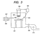
- 238000010586 diagram Methods 0.000 description 3
- 239000008151 electrolyte solution Substances 0.000 description 3
- 238000001704 evaporation Methods 0.000 description 3
- 230000008020 evaporation Effects 0.000 description 3
- 239000010931 gold Substances 0.000 description 3
- 230000006872 improvement Effects 0.000 description 3
- 239000007788 liquid Substances 0.000 description 3
- 238000000691 measurement method Methods 0.000 description 3
- 238000007254 oxidation reaction Methods 0.000 description 3
- 230000001105 regulatory effect Effects 0.000 description 3
- 230000000717 retained effect Effects 0.000 description 3
- UFHFLCQGNIYNRP-UHFFFAOYSA-N Hydrogen Chemical compound [H][H] UFHFLCQGNIYNRP-UHFFFAOYSA-N 0.000 description 2
- 230000002159 abnormal effect Effects 0.000 description 2
- 238000011109 contamination Methods 0.000 description 2
- 238000004070 electrodeposition Methods 0.000 description 2
- 229910052737 gold Inorganic materials 0.000 description 2
- 125000005843 halogen group Chemical group 0.000 description 2
- 239000001257 hydrogen Substances 0.000 description 2
- 229910052739 hydrogen Inorganic materials 0.000 description 2
- 230000007246 mechanism Effects 0.000 description 2
- 230000003647 oxidation Effects 0.000 description 2
- 230000008569 process Effects 0.000 description 2
- 238000002207 thermal evaporation Methods 0.000 description 2
- 238000007738 vacuum evaporation Methods 0.000 description 2
- 238000005406 washing Methods 0.000 description 2
- ONDPHDOFVYQSGI-UHFFFAOYSA-N zinc nitrate Chemical compound [Zn+2].[O-][N+]([O-])=O.[O-][N+]([O-])=O ONDPHDOFVYQSGI-UHFFFAOYSA-N 0.000 description 2
- NHNBFGGVMKEFGY-UHFFFAOYSA-N Nitrate Chemical compound [O-][N+]([O-])=O NHNBFGGVMKEFGY-UHFFFAOYSA-N 0.000 description 1
- 239000004642 Polyimide Substances 0.000 description 1
- XUIMIQQOPSSXEZ-UHFFFAOYSA-N Silicon Chemical compound [Si] XUIMIQQOPSSXEZ-UHFFFAOYSA-N 0.000 description 1
- 229910000831 Steel Inorganic materials 0.000 description 1
- LEVVHYCKPQWKOP-UHFFFAOYSA-N [Si].[Ge] Chemical compound [Si].[Ge] LEVVHYCKPQWKOP-UHFFFAOYSA-N 0.000 description 1
- 238000010521 absorption reaction Methods 0.000 description 1
- 239000012300 argon atmosphere Substances 0.000 description 1
- 230000015572 biosynthetic process Effects 0.000 description 1
- 150000001720 carbohydrates Chemical class 0.000 description 1
- 235000014633 carbohydrates Nutrition 0.000 description 1
- 229910052799 carbon Inorganic materials 0.000 description 1
- 239000000919 ceramic Substances 0.000 description 1
- 230000008859 change Effects 0.000 description 1
- 150000001875 compounds Chemical class 0.000 description 1
- 238000012790 confirmation Methods 0.000 description 1
- 238000005260 corrosion Methods 0.000 description 1
- 230000007547 defect Effects 0.000 description 1
- 230000002542 deteriorative effect Effects 0.000 description 1
- 238000006073 displacement reaction Methods 0.000 description 1
- 238000001035 drying Methods 0.000 description 1
- 238000002474 experimental method Methods 0.000 description 1
- 239000011521 glass Substances 0.000 description 1
- PCHJSUWPFVWCPO-UHFFFAOYSA-N gold Chemical compound [Au] PCHJSUWPFVWCPO-UHFFFAOYSA-N 0.000 description 1
- 238000007654 immersion Methods 0.000 description 1
- 239000012535 impurity Substances 0.000 description 1
- PJXISJQVUVHSOJ-UHFFFAOYSA-N indium(III) oxide Inorganic materials [O-2].[O-2].[O-2].[In+3].[In+3] PJXISJQVUVHSOJ-UHFFFAOYSA-N 0.000 description 1
- 238000002347 injection Methods 0.000 description 1
- 239000007924 injection Substances 0.000 description 1
- 230000001788 irregular Effects 0.000 description 1
- 230000031700 light absorption Effects 0.000 description 1
- 238000005268 plasma chemical vapour deposition Methods 0.000 description 1
- 229910021420 polycrystalline silicon Inorganic materials 0.000 description 1
- 229920001721 polyimide Polymers 0.000 description 1
- 230000002265 prevention Effects 0.000 description 1
- 239000011241 protective layer Substances 0.000 description 1
- 230000003014 reinforcing effect Effects 0.000 description 1
- 239000011347 resin Substances 0.000 description 1
- 229920005989 resin Polymers 0.000 description 1
- 230000002441 reversible effect Effects 0.000 description 1
- 238000005096 rolling process Methods 0.000 description 1
- 229910052710 silicon Inorganic materials 0.000 description 1
- 239000010703 silicon Substances 0.000 description 1
- HBMJWWWQQXIZIP-UHFFFAOYSA-N silicon carbide Chemical compound [Si+]#[C-] HBMJWWWQQXIZIP-UHFFFAOYSA-N 0.000 description 1
- 229910010271 silicon carbide Inorganic materials 0.000 description 1
- 239000010944 silver (metal) Substances 0.000 description 1
- 229910000679 solder Inorganic materials 0.000 description 1
- 238000005507 spraying Methods 0.000 description 1
- 239000010959 steel Substances 0.000 description 1
- 238000003756 stirring Methods 0.000 description 1
- 239000000126 substance Substances 0.000 description 1
Images


Classifications
-
- H—ELECTRICITY
- H01—ELECTRIC ELEMENTS
- H01L—SEMICONDUCTOR DEVICES NOT COVERED BY CLASS H10
- H01L31/00—Semiconductor devices sensitive to infrared radiation, light, electromagnetic radiation of shorter wavelength or corpuscular radiation and specially adapted either for the conversion of the energy of such radiation into electrical energy or for the control of electrical energy by such radiation; Processes or apparatus specially adapted for the manufacture or treatment thereof or of parts thereof; Details thereof
- H01L31/18—Processes or apparatus specially adapted for the manufacture or treatment of these devices or of parts thereof
- H01L31/1884—Manufacture of transparent electrodes, e.g. TCO, ITO
-
- C—CHEMISTRY; METALLURGY
- C25—ELECTROLYTIC OR ELECTROPHORETIC PROCESSES; APPARATUS THEREFOR
- C25D—PROCESSES FOR THE ELECTROLYTIC OR ELECTROPHORETIC PRODUCTION OF COATINGS; ELECTROFORMING; APPARATUS THEREFOR
- C25D9/00—Electrolytic coating other than with metals
- C25D9/04—Electrolytic coating other than with metals with inorganic materials
-
- H—ELECTRICITY
- H01—ELECTRIC ELEMENTS
- H01L—SEMICONDUCTOR DEVICES NOT COVERED BY CLASS H10
- H01L31/00—Semiconductor devices sensitive to infrared radiation, light, electromagnetic radiation of shorter wavelength or corpuscular radiation and specially adapted either for the conversion of the energy of such radiation into electrical energy or for the control of electrical energy by such radiation; Processes or apparatus specially adapted for the manufacture or treatment thereof or of parts thereof; Details thereof
- H01L31/04—Semiconductor devices sensitive to infrared radiation, light, electromagnetic radiation of shorter wavelength or corpuscular radiation and specially adapted either for the conversion of the energy of such radiation into electrical energy or for the control of electrical energy by such radiation; Processes or apparatus specially adapted for the manufacture or treatment thereof or of parts thereof; Details thereof adapted as photovoltaic [PV] conversion devices
- H01L31/054—Optical elements directly associated or integrated with the PV cell, e.g. light-reflecting means or light-concentrating means
- H01L31/056—Optical elements directly associated or integrated with the PV cell, e.g. light-reflecting means or light-concentrating means the light-reflecting means being of the back surface reflector [BSR] type
-
- H—ELECTRICITY
- H01—ELECTRIC ELEMENTS
- H01L—SEMICONDUCTOR DEVICES NOT COVERED BY CLASS H10
- H01L31/00—Semiconductor devices sensitive to infrared radiation, light, electromagnetic radiation of shorter wavelength or corpuscular radiation and specially adapted either for the conversion of the energy of such radiation into electrical energy or for the control of electrical energy by such radiation; Processes or apparatus specially adapted for the manufacture or treatment thereof or of parts thereof; Details thereof
- H01L31/18—Processes or apparatus specially adapted for the manufacture or treatment of these devices or of parts thereof
- H01L31/186—Particular post-treatment for the devices, e.g. annealing, impurity gettering, short-circuit elimination, recrystallisation
- H01L31/1864—Annealing
-
- Y—GENERAL TAGGING OF NEW TECHNOLOGICAL DEVELOPMENTS; GENERAL TAGGING OF CROSS-SECTIONAL TECHNOLOGIES SPANNING OVER SEVERAL SECTIONS OF THE IPC; TECHNICAL SUBJECTS COVERED BY FORMER USPC CROSS-REFERENCE ART COLLECTIONS [XRACs] AND DIGESTS
- Y02—TECHNOLOGIES OR APPLICATIONS FOR MITIGATION OR ADAPTATION AGAINST CLIMATE CHANGE
- Y02E—REDUCTION OF GREENHOUSE GAS [GHG] EMISSIONS, RELATED TO ENERGY GENERATION, TRANSMISSION OR DISTRIBUTION
- Y02E10/00—Energy generation through renewable energy sources
- Y02E10/50—Photovoltaic [PV] energy
- Y02E10/52—PV systems with concentrators
-
- Y—GENERAL TAGGING OF NEW TECHNOLOGICAL DEVELOPMENTS; GENERAL TAGGING OF CROSS-SECTIONAL TECHNOLOGIES SPANNING OVER SEVERAL SECTIONS OF THE IPC; TECHNICAL SUBJECTS COVERED BY FORMER USPC CROSS-REFERENCE ART COLLECTIONS [XRACs] AND DIGESTS
- Y02—TECHNOLOGIES OR APPLICATIONS FOR MITIGATION OR ADAPTATION AGAINST CLIMATE CHANGE
- Y02P—CLIMATE CHANGE MITIGATION TECHNOLOGIES IN THE PRODUCTION OR PROCESSING OF GOODS
- Y02P70/00—Climate change mitigation technologies in the production process for final industrial or consumer products
- Y02P70/50—Manufacturing or production processes characterised by the final manufactured product
Applications Claiming Priority (2)
| Application Number | Priority Date | Filing Date | Title |
|---|---|---|---|
| JP2003081785A JP2004289034A (ja) | 2003-03-25 | 2003-03-25 | 酸化亜鉛膜の処理方法、それを用いた光起電力素子の製造方法 |
| JP2003081785 | 2003-03-25 |
Publications (1)
| Publication Number | Publication Date |
|---|---|
| EP1465262A2 true EP1465262A2 (fr) | 2004-10-06 |
Family
ID=32844580
Family Applications (1)
| Application Number | Title | Priority Date | Filing Date |
|---|---|---|---|
| EP04007124A Withdrawn EP1465262A2 (fr) | 2003-03-25 | 2004-03-24 | Procédé de traitement avec une couche d'oxyde de zinc et de fabrication d'un dispositif photovoltaique et son utilisation |
Country Status (5)
| Country | Link |
|---|---|
| US (1) | US7282132B2 (fr) |
| EP (1) | EP1465262A2 (fr) |
| JP (1) | JP2004289034A (fr) |
| CN (1) | CN1532951A (fr) |
| AU (1) | AU2004201191A1 (fr) |
Cited By (2)
| Publication number | Priority date | Publication date | Assignee | Title |
|---|---|---|---|---|
| DE102007024986A1 (de) | 2007-05-28 | 2008-12-04 | Forschungszentrum Jülich GmbH | Temperaturstabile TCO-Schicht, Verfahren zur Herstellung und Anwendung |
| EP2138608A1 (fr) * | 2008-06-24 | 2009-12-30 | Nederlandse Organisatie voor toegepast- natuurwetenschappelijk onderzoek TNO | Procédé de préparation d'un film transparent et conducteur sur un substrat |
Families Citing this family (34)
| Publication number | Priority date | Publication date | Assignee | Title |
|---|---|---|---|---|
| JP2006329662A (ja) * | 2005-05-23 | 2006-12-07 | Ulvac Japan Ltd | 質量分析装置およびその使用方法 |
| JP5037808B2 (ja) | 2005-10-20 | 2012-10-03 | キヤノン株式会社 | アモルファス酸化物を用いた電界効果型トランジスタ、及び該トランジスタを用いた表示装置 |
| JP5127183B2 (ja) * | 2006-08-23 | 2013-01-23 | キヤノン株式会社 | アモルファス酸化物半導体膜を用いた薄膜トランジスタの製造方法 |
| JP5305630B2 (ja) | 2006-12-05 | 2013-10-02 | キヤノン株式会社 | ボトムゲート型薄膜トランジスタの製造方法及び表示装置の製造方法 |
| US8143115B2 (en) * | 2006-12-05 | 2012-03-27 | Canon Kabushiki Kaisha | Method for manufacturing thin film transistor using oxide semiconductor and display apparatus |
| KR101340514B1 (ko) * | 2007-01-24 | 2013-12-12 | 삼성디스플레이 주식회사 | 박막 트랜지스터 기판 및 이의 제조 방법 |
| JP5354862B2 (ja) * | 2007-02-19 | 2013-11-27 | キヤノン株式会社 | アモルファス絶縁体膜及び薄膜トランジスタ |
| US20080286907A1 (en) * | 2007-05-16 | 2008-11-20 | Xerox Corporation | Semiconductor layer for thin film transistors |
| US8071179B2 (en) | 2007-06-29 | 2011-12-06 | Stion Corporation | Methods for infusing one or more materials into nano-voids if nanoporous or nanostructured materials |
| JP5213422B2 (ja) * | 2007-12-04 | 2013-06-19 | キヤノン株式会社 | 絶縁層を有する酸化物半導体素子およびそれを用いた表示装置 |
| FR2932610B1 (fr) * | 2008-06-11 | 2010-11-12 | Saint Gobain | Cellule photovoltaique et substrat de cellule photovoltaique |
| FR2932611B1 (fr) * | 2008-06-11 | 2010-11-12 | Saint Gobain | Cellule photovoltaique et substrat de cellule photovoltaique |
| US8129718B2 (en) * | 2008-08-28 | 2012-03-06 | Canon Kabushiki Kaisha | Amorphous oxide semiconductor and thin film transistor using the same |
| US7947524B2 (en) | 2008-09-30 | 2011-05-24 | Stion Corporation | Humidity control and method for thin film photovoltaic materials |
| US8741689B2 (en) * | 2008-10-01 | 2014-06-03 | Stion Corporation | Thermal pre-treatment process for soda lime glass substrate for thin film photovoltaic materials |
| US20110018103A1 (en) * | 2008-10-02 | 2011-01-27 | Stion Corporation | System and method for transferring substrates in large scale processing of cigs and/or cis devices |
| US20100206370A1 (en) * | 2009-02-18 | 2010-08-19 | Qualcomm Incorporated | Photovoltaic Cell Efficiency Using Through Silicon Vias |
| WO2010110870A1 (fr) * | 2009-03-25 | 2010-09-30 | Xunlight Corporation | Cellules photovoltaïques avec substrat en acier plaqué |
| TWI379430B (en) * | 2009-04-16 | 2012-12-11 | Atomic Energy Council | A method of fabricating a thin interface for internal light reflection and impurities isolation |
| US8241943B1 (en) | 2009-05-08 | 2012-08-14 | Stion Corporation | Sodium doping method and system for shaped CIGS/CIS based thin film solar cells |
| US8372684B1 (en) | 2009-05-14 | 2013-02-12 | Stion Corporation | Method and system for selenization in fabricating CIGS/CIS solar cells |
| US8507786B1 (en) | 2009-06-27 | 2013-08-13 | Stion Corporation | Manufacturing method for patterning CIGS/CIS solar cells |
| US8398772B1 (en) | 2009-08-18 | 2013-03-19 | Stion Corporation | Method and structure for processing thin film PV cells with improved temperature uniformity |
| US8859880B2 (en) * | 2010-01-22 | 2014-10-14 | Stion Corporation | Method and structure for tiling industrial thin-film solar devices |
| CN102201499A (zh) * | 2010-03-25 | 2011-09-28 | 日本麦可罗尼克斯股份有限公司 | 电气处理装置及方法、以及探测单元 |
| US9096930B2 (en) | 2010-03-29 | 2015-08-04 | Stion Corporation | Apparatus for manufacturing thin film photovoltaic devices |
| US8142521B2 (en) * | 2010-03-29 | 2012-03-27 | Stion Corporation | Large scale MOCVD system for thin film photovoltaic devices |
| US8461061B2 (en) | 2010-07-23 | 2013-06-11 | Stion Corporation | Quartz boat method and apparatus for thin film thermal treatment |
| JP2012033836A (ja) | 2010-08-03 | 2012-02-16 | Canon Inc | トップゲート型薄膜トランジスタ及びこれを備えた表示装置 |
| US10090799B2 (en) * | 2012-01-10 | 2018-10-02 | Pvilion, Inc. | Tensioned sheet-metal based solar panels and structures for supporting the same |
| CN104465321B (zh) * | 2014-11-21 | 2018-02-16 | 河南大学 | 一种制备光电薄膜的方法 |
| CN106935666B (zh) * | 2017-04-21 | 2019-05-03 | 常州亿晶光电科技有限公司 | 一种光伏材料及制备方法和用途 |
| CN109599470B (zh) * | 2018-12-06 | 2020-08-25 | 中国科学技术大学 | 一种降低掺镁氧化锌薄膜电阻率的方法 |
| US11352710B2 (en) * | 2019-09-30 | 2022-06-07 | Abdurrahman Ildeniz | Leak free brush electroplating system |
Family Cites Families (45)
| Publication number | Priority date | Publication date | Assignee | Title |
|---|---|---|---|---|
| JPH04119843A (ja) | 1990-09-11 | 1992-04-21 | Toray Ind Inc | 止着タイルカーペット |
| AU662360B2 (en) | 1991-10-22 | 1995-08-31 | Canon Kabushiki Kaisha | Photovoltaic device |
| JP3045612B2 (ja) * | 1992-06-22 | 2000-05-29 | 東洋鋼鈑株式会社 | 高耐食性ニッケルめっき鋼帯およびその製造法 |
| JP3170105B2 (ja) | 1993-07-01 | 2001-05-28 | キヤノン株式会社 | 太陽電池モジュール |
| JPH07302926A (ja) | 1994-04-30 | 1995-11-14 | Canon Inc | 太陽電池モジュール |
| JP3618802B2 (ja) | 1994-11-04 | 2005-02-09 | キヤノン株式会社 | 太陽電池モジュール |
| JP3273294B2 (ja) | 1995-02-13 | 2002-04-08 | 大阪市 | 酸化亜鉛膜作製用電解液 |
| JP2915327B2 (ja) | 1995-07-19 | 1999-07-05 | キヤノン株式会社 | 太陽電池モジュール及びその製造方法 |
| CN1169228C (zh) | 1995-08-24 | 2004-09-29 | 佳能株式会社 | 太阳能电池组件,其制造方法以及建筑物构件 |
| DE69702277T2 (de) * | 1996-03-06 | 2001-03-01 | Canon Kk | Verfahren zur Herstellung einer Dünnzinkoxidfilm und Verfahren zur Herstellung eines Substrats einer Halbleiteranordnung und Verfahren zur Herstellung einer photoelektrischen Umwandlungsvorrichtung unter Verwendung dieser Film |
| US6172296B1 (en) | 1996-05-17 | 2001-01-09 | Canon Kabushiki Kaisha | Photovoltaic cell |
| JPH10112549A (ja) | 1996-10-08 | 1998-04-28 | Canon Inc | 太陽電池モジュール |
| JP4154004B2 (ja) | 1997-01-06 | 2008-09-24 | キヤノン株式会社 | 太陽電池モジュールの製造方法 |
| JPH10209474A (ja) | 1997-01-21 | 1998-08-07 | Canon Inc | 太陽電池モジュール及びその製造方法 |
| JPH10140373A (ja) | 1997-02-04 | 1998-05-26 | Canon Inc | 酸化亜鉛薄膜の製造方法、それを用いた半導体素子基板及び光起電力素子 |
| JPH10233521A (ja) | 1997-02-19 | 1998-09-02 | Canon Inc | 太陽電池モジュール、及びそれを用いた太陽電池一体型建材、太陽光発電装置 |
| JPH11135820A (ja) | 1997-08-27 | 1999-05-21 | Canon Inc | 太陽電池モジュール及び太陽電池モジュール用補強部材 |
| JP3658160B2 (ja) | 1997-11-17 | 2005-06-08 | キヤノン株式会社 | モールドレス半導体装置 |
| JP3423631B2 (ja) | 1998-02-05 | 2003-07-07 | キヤノン株式会社 | 酸化亜鉛薄膜の形成方法、それを用いた半導体素子基板の製造方法及び光起電力素子の製造方法 |
| JPH11233801A (ja) | 1998-02-17 | 1999-08-27 | Canon Inc | 微結晶シリコン膜の形成方法、および光起電力素子 |
| JP4208281B2 (ja) | 1998-02-26 | 2009-01-14 | キヤノン株式会社 | 積層型光起電力素子 |
| US6175075B1 (en) | 1998-04-21 | 2001-01-16 | Canon Kabushiki Kaisha | Solar cell module excelling in reliability |
| JP2000286437A (ja) | 1998-06-12 | 2000-10-13 | Canon Inc | 太陽電池モジュールおよび製造方法 |
| EP0975027A2 (fr) * | 1998-07-23 | 2000-01-26 | Sony Corporation | Dispositif émetteur de lumière et méthode de fabrication |
| US6544877B1 (en) | 1998-11-24 | 2003-04-08 | Canon Kabushiki Kaisha | Method of producing thin film of zinc oxide, process for manufacturing photovoltaic element using its method, and photovoltaic element |
| US6414236B1 (en) | 1999-06-30 | 2002-07-02 | Canon Kabushiki Kaisha | Solar cell module |
| US6472248B2 (en) | 1999-07-04 | 2002-10-29 | Canon Kabushiki Kaisha | Microcrystalline series photovoltaic element and process for fabrication of same |
| JP3445187B2 (ja) | 1999-08-03 | 2003-09-08 | キヤノン株式会社 | 半導体素子の欠陥補償方法 |
| JP3445203B2 (ja) | 1999-11-30 | 2003-09-08 | キヤノン株式会社 | 酸化亜鉛電析方法および装置 |
| JP4336442B2 (ja) | 2000-05-23 | 2009-09-30 | キヤノン株式会社 | 太陽電池モジュール |
| JP2002083990A (ja) | 2000-07-06 | 2002-03-22 | Canon Inc | 光起電力素子集合体及びそれを用いた太陽電池モジュールと太陽電池モジュールの製造方法 |
| US6576112B2 (en) | 2000-09-19 | 2003-06-10 | Canon Kabushiki Kaisha | Method of forming zinc oxide film and process for producing photovoltaic device using it |
| JP2002206168A (ja) | 2000-10-24 | 2002-07-26 | Canon Inc | シリコン系薄膜の形成方法、シリコン系半導体層の形成方法及び光起電力素子 |
| US6433061B1 (en) * | 2000-10-24 | 2002-08-13 | Noveon Ip Holdings Corp. | Rheology modifying copolymer composition |
| JP2002134772A (ja) | 2000-10-24 | 2002-05-10 | Canon Inc | シリコン系薄膜及び光起電力素子 |
| JP2002237606A (ja) | 2000-12-04 | 2002-08-23 | Canon Inc | 太陽電池用基板、それを用いた太陽電池及び太陽電池の製造方法 |
| JP2002198555A (ja) | 2000-12-26 | 2002-07-12 | Canon Inc | 半導体素子搭載用基板及び該基板を使用した半導体デバイス |
| JP4050902B2 (ja) | 2000-12-28 | 2008-02-20 | 株式会社半導体エネルギー研究所 | 半導体装置の作製方法 |
| US7534977B2 (en) | 2000-12-28 | 2009-05-19 | Semiconductor Energy Laboratory Co., Ltd. | Heat treatment apparatus and method of manufacturing a semiconductor device |
| JP2002305315A (ja) | 2001-01-31 | 2002-10-18 | Canon Inc | 半導体素子の形成方法及び半導体素子 |
| US6706336B2 (en) | 2001-02-02 | 2004-03-16 | Canon Kabushiki Kaisha | Silicon-based film, formation method therefor and photovoltaic element |
| US6858308B2 (en) | 2001-03-12 | 2005-02-22 | Canon Kabushiki Kaisha | Semiconductor element, and method of forming silicon-based film |
| JP2003007629A (ja) | 2001-04-03 | 2003-01-10 | Canon Inc | シリコン系膜の形成方法、シリコン系膜および半導体素子 |
| JP2003046496A (ja) | 2001-07-31 | 2003-02-14 | Canon Inc | 情報管理方法、情報管理システム及び処理装置 |
| JP4240933B2 (ja) | 2002-07-18 | 2009-03-18 | キヤノン株式会社 | 積層体形成方法 |
-
2003
- 2003-03-25 JP JP2003081785A patent/JP2004289034A/ja not_active Withdrawn
-
2004
- 2004-03-22 US US10/805,323 patent/US7282132B2/en not_active Expired - Fee Related
- 2004-03-22 AU AU2004201191A patent/AU2004201191A1/en not_active Abandoned
- 2004-03-24 EP EP04007124A patent/EP1465262A2/fr not_active Withdrawn
- 2004-03-25 CN CNA2004100085843A patent/CN1532951A/zh active Pending
Cited By (3)
| Publication number | Priority date | Publication date | Assignee | Title |
|---|---|---|---|---|
| DE102007024986A1 (de) | 2007-05-28 | 2008-12-04 | Forschungszentrum Jülich GmbH | Temperaturstabile TCO-Schicht, Verfahren zur Herstellung und Anwendung |
| WO2008145099A1 (fr) | 2007-05-28 | 2008-12-04 | Helmholtz Zentrum Berlin Für Materialien Und Energie Gmbh | Couche de tco résistant à la température, son procédé de réalisation et son utilisation |
| EP2138608A1 (fr) * | 2008-06-24 | 2009-12-30 | Nederlandse Organisatie voor toegepast- natuurwetenschappelijk onderzoek TNO | Procédé de préparation d'un film transparent et conducteur sur un substrat |
Also Published As
| Publication number | Publication date |
|---|---|
| JP2004289034A (ja) | 2004-10-14 |
| AU2004201191A1 (en) | 2004-10-14 |
| US7282132B2 (en) | 2007-10-16 |
| US20040191949A1 (en) | 2004-09-30 |
| CN1532951A (zh) | 2004-09-29 |
Similar Documents
| Publication | Publication Date | Title |
|---|---|---|
| US7282132B2 (en) | Zinc oxide film treatment method and method of manufacturing photovoltaic device utilizing the same | |
| JP3667178B2 (ja) | 酸化亜鉛薄膜の製造方法、それを用いた光起電力素子の製造方法、及び光起電力素子 | |
| US6576112B2 (en) | Method of forming zinc oxide film and process for producing photovoltaic device using it | |
| US20040191950A1 (en) | Method of producing photovoltaic device | |
| EP0538840B1 (fr) | Dispositif photovoltaique | |
| JP2002167695A (ja) | 酸化亜鉛膜の形成方法、それを用いた光起電力素子の製造方法 | |
| JP3327811B2 (ja) | 酸化亜鉛薄膜の製造方法、それを用いた光起電力素子及び半導体素子基板の製造方法 | |
| US7445952B2 (en) | Method of forming laminate and method of manufacturing photovoltaic device | |
| EP0935296A2 (fr) | Méthode de formation d'une couche mince d'oxyde de zinc et d' un substrat pour un élément semiconducteur et élément photovoltaique pourvu de cette couche mince d'oxyde de zinc | |
| US6812499B2 (en) | Silicon-based film and photovoltaic element | |
| US5798284A (en) | Process for fabricating array of photovoltaic elements connected in series | |
| JP2006269607A (ja) | 光起電力素子の製造方法 | |
| US6544877B1 (en) | Method of producing thin film of zinc oxide, process for manufacturing photovoltaic element using its method, and photovoltaic element | |
| JP3618986B2 (ja) | 光起電力素子の製造方法 | |
| JP3535757B2 (ja) | 酸化亜鉛膜の製造方法と光起電力素子の製造方法と半導体素子基板の製造方法 | |
| JP3006701B2 (ja) | 薄膜半導体太陽電池 | |
| JP2000004036A (ja) | 微結晶半導体層の形成方法、および光起電力素子 | |
| JP3437475B2 (ja) | 酸化亜鉛膜の形成方法及び該酸化亜鉛膜を用いた光起電力素子 | |
| JP2002134773A (ja) | 光起電力素子 | |
| US20030085129A1 (en) | Method of forming zinc oxide film, method of producing semiconductor element substrate using same, and method of producing photovoltaic element | |
| JP3368176B2 (ja) | 酸化亜鉛薄膜の製造方法、それを用いた光起電力素子及び半導体素子基板の製造方法 | |
| JP2001244488A (ja) | 光起電力素子 | |
| JP3445132B2 (ja) | 酸化亜鉛薄膜の製造方法、それを用いた半導体素子基板の製造方法、光電変換素子の製造方法、酸化亜鉛薄膜、半導体素子基板及び光電変換素子 | |
| JP2006093477A (ja) | 酸化亜鉛層及び光起電力素子 | |
| JP3524366B2 (ja) | 酸化亜鉛薄膜形成装置、酸化亜鉛薄膜の形成方法、並びにそれを用いた半導体素子基板及び光起電力素子の製造方法 |
Legal Events
| Date | Code | Title | Description |
|---|---|---|---|
| PUAI | Public reference made under article 153(3) epc to a published international application that has entered the european phase |
Free format text: ORIGINAL CODE: 0009012 |
|
| AK | Designated contracting states |
Kind code of ref document: A2 Designated state(s): AT BE BG CH CY CZ DE DK EE ES FI FR GB GR HU IE IT LI LU MC NL PL PT RO SE SI SK TR |
|
| AX | Request for extension of the european patent |
Extension state: AL LT LV MK |
|
| STAA | Information on the status of an ep patent application or granted ep patent |
Free format text: STATUS: THE APPLICATION HAS BEEN WITHDRAWN |
|
| 18W | Application withdrawn |
Effective date: 20060724 |