EP1237200A2 - Hochspannungshalbleiteranordnung und Verfahren zur Herstellung - Google Patents
Hochspannungshalbleiteranordnung und Verfahren zur Herstellung Download PDFInfo
- Publication number
- EP1237200A2 EP1237200A2 EP02004311A EP02004311A EP1237200A2 EP 1237200 A2 EP1237200 A2 EP 1237200A2 EP 02004311 A EP02004311 A EP 02004311A EP 02004311 A EP02004311 A EP 02004311A EP 1237200 A2 EP1237200 A2 EP 1237200A2
- Authority
- EP
- European Patent Office
- Prior art keywords
- layer
- buffer layer
- substrate
- conductivity type
- forming
- Prior art date
- Legal status (The legal status is an assumption and is not a legal conclusion. Google has not performed a legal analysis and makes no representation as to the accuracy of the status listed.)
- Withdrawn
Links
- 238000000034 method Methods 0.000 title claims description 54
- 238000004519 manufacturing process Methods 0.000 title claims description 53
- 239000004065 semiconductor Substances 0.000 title claims description 31
- 239000000758 substrate Substances 0.000 claims description 66
- 239000012535 impurity Substances 0.000 claims description 44
- 229910021426 porous silicon Inorganic materials 0.000 claims description 13
- 238000005304 joining Methods 0.000 claims description 5
- 238000002347 injection Methods 0.000 abstract description 3
- 239000007924 injection Substances 0.000 abstract description 3
- 230000010355 oscillation Effects 0.000 abstract description 3
- 150000002500 ions Chemical class 0.000 description 15
- XUIMIQQOPSSXEZ-UHFFFAOYSA-N Silicon Chemical compound [Si] XUIMIQQOPSSXEZ-UHFFFAOYSA-N 0.000 description 12
- 229910052710 silicon Inorganic materials 0.000 description 12
- 239000010703 silicon Substances 0.000 description 12
- 238000005530 etching Methods 0.000 description 11
- 230000015556 catabolic process Effects 0.000 description 9
- 230000003068 static effect Effects 0.000 description 9
- OAICVXFJPJFONN-UHFFFAOYSA-N Phosphorus Chemical compound [P] OAICVXFJPJFONN-UHFFFAOYSA-N 0.000 description 7
- 229910052796 boron Inorganic materials 0.000 description 7
- 229910052698 phosphorus Inorganic materials 0.000 description 7
- 239000011574 phosphorus Substances 0.000 description 7
- ZOXJGFHDIHLPTG-UHFFFAOYSA-N Boron Chemical compound [B] ZOXJGFHDIHLPTG-UHFFFAOYSA-N 0.000 description 6
- 238000010438 heat treatment Methods 0.000 description 6
- 238000005411 Van der Waals force Methods 0.000 description 3
- 238000000137 annealing Methods 0.000 description 3
- 238000010586 diagram Methods 0.000 description 3
- 238000009792 diffusion process Methods 0.000 description 3
- 238000005224 laser annealing Methods 0.000 description 3
- 238000005245 sintering Methods 0.000 description 3
- 230000000694 effects Effects 0.000 description 2
- 238000004904 shortening Methods 0.000 description 2
- QVGXLLKOCUKJST-UHFFFAOYSA-N atomic oxygen Chemical compound [O] QVGXLLKOCUKJST-UHFFFAOYSA-N 0.000 description 1
- -1 boron ions Chemical class 0.000 description 1
- 239000000969 carrier Substances 0.000 description 1
- 238000001312 dry etching Methods 0.000 description 1
- 239000000463 material Substances 0.000 description 1
- 229910052760 oxygen Inorganic materials 0.000 description 1
- 239000001301 oxygen Substances 0.000 description 1
- 238000000926 separation method Methods 0.000 description 1
- 230000000087 stabilizing effect Effects 0.000 description 1
- 239000000126 substance Substances 0.000 description 1
Images


Classifications
-
- H—ELECTRICITY
- H10—SEMICONDUCTOR DEVICES; ELECTRIC SOLID-STATE DEVICES NOT OTHERWISE PROVIDED FOR
- H10D—INORGANIC ELECTRIC SEMICONDUCTOR DEVICES
- H10D12/00—Bipolar devices controlled by the field effect, e.g. insulated-gate bipolar transistors [IGBT]
- H10D12/01—Manufacture or treatment
- H10D12/031—Manufacture or treatment of IGBTs
- H10D12/032—Manufacture or treatment of IGBTs of vertical IGBTs
- H10D12/038—Manufacture or treatment of IGBTs of vertical IGBTs having a recessed gate, e.g. trench-gate IGBTs
-
- H—ELECTRICITY
- H10—SEMICONDUCTOR DEVICES; ELECTRIC SOLID-STATE DEVICES NOT OTHERWISE PROVIDED FOR
- H10D—INORGANIC ELECTRIC SEMICONDUCTOR DEVICES
- H10D12/00—Bipolar devices controlled by the field effect, e.g. insulated-gate bipolar transistors [IGBT]
- H10D12/411—Insulated-gate bipolar transistors [IGBT]
- H10D12/441—Vertical IGBTs
- H10D12/461—Vertical IGBTs having non-planar surfaces, e.g. having trenches, recesses or pillars in the surfaces of the emitter, base or collector regions
- H10D12/481—Vertical IGBTs having non-planar surfaces, e.g. having trenches, recesses or pillars in the surfaces of the emitter, base or collector regions having gate structures on slanted surfaces, on vertical surfaces, or in grooves, e.g. trench gate IGBTs
Definitions
- the present invention relates to a semiconductor device which withstands a high voltage, for example, an IGBT (Insulating Gate Bipolar Transistor).
- IGBT Insulating Gate Bipolar Transistor
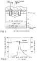
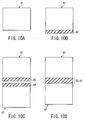
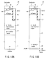
- FIG. 18A shows a conventional vertical IGBT of a punch-through type.
- an n + -type buffer layer hereinafter referred to as the n + buffer layer 12 and an n - -type high resistance layer (hereinafter referred to as the n - high resistance layer) 13 are formed by epitaxial growth on a p + substrate 11.
- a p-type base layer 14 is formed in a surface region of the n - high resistance layer 13.
- An n + source region (cathode) 15 is formed in a surface region of the base layer 14.
- a trench-type gate electrode 16 is formed in the source region 15, the base layer 14 and the n - high resistance layer 13. The gate electrode 16 is insulated from the source region 15, the base layer 14 and the n - high resistance layer 13 by a gate insulating film 17.
- the IGBT 10 is produced with, for example, an epitaxial substrate, on which an epitaxial layer is formed in advance.
- the epitaxial substrate is disadvantageous in that the cost for manufacturing an element is high since the wafer is expensive.
- the substrate 11 which is relatively thick, is used as a p + drain layer (anode). Therefore, to lower the carrier injection efficiency, it is necessary to control the lifetime.
- a process for shortening the lifetime of 5-10 ⁇ s to about 100 ns is performed. As a result, a high-speed turn-off characteristic can be obtained, although the process has a drawback that the on-state voltage rises. This is because the carrier density in the n - high resistance layer 13 is lowered by shortening the lifetime.
- the on-state voltage can be lower if the lifetime is not shortened.
- the turn-off time will be considerably long.
- a depletion layer extends from the base layer 14 due to a voltage applied to the element when the current is turned off.
- the depletion layer reaches the n + buffer layer 12, it is immediately stopped. For this reason, the drain current is instantaneously dropped to zero, so that the drain voltage oscillates, resulting in generation of noise.
- FIG. 18B shows another conventional IGBT, in which the characteristic of the element described above is improved.
- the IGBT 20 shown in FIG. 18B has a p + anode structure injected with a small amount of impurities at a low dose, which is adopted in a non-punch-through IGBT. Therefore, the operation speed can be increased without controlling the lifetime.
- the IGBT 20 comprises an n-type buffer layer (hereinafter referred to as the n buffer layer) 23 formed between the n - high resistance layer 21 and the p + drain layer (anode) 22.
- the n buffer layer 23 maintains the static breakdown voltage.
- the drain layer 22 must be injected with impurities at a low dose but have such a high concentration in the surface portion thereof that can establish ohmic contact. Therefore, the region where the impurities injected to form the drain layer 22 are diffused must be limited to a very shallow depth.
- the total thickness of the IGBT is equal to the thickness of the n - high resistance layer 21, which is determined in accordance with the static breakdown voltage, plus the thickness of the n buffer layer 23 and the p + drain layer 22. More specifically, in the case of an element of the 600V voltage series, the total thickness is as small as about 60 ⁇ m.
- the element is very thin. Therefore, for example, when the element is lapped, if the thickness is thinner or thicker than the design value by several microns, the thickness of the buffer layer 23 is varied. The variation in thickness of the buffer layer 23 is reflected on a variation in dose into the buffer layer 23, with the result that the characteristics of the element are considerably influenced. Therefore, when the element is manufactured, it is necessary to finish the element to the designed thickness with a minimum error.
- the lapping error is ⁇ 5 to 10 ⁇ m, which is significantly large relative to the overall thickness of 60 ⁇ m.
- a semiconductor device comprising:
- a method for manufacturing a semiconductor device comprising: forming a high resistance layer of a first conductivity type on a main surface of a first buffer layer of the first conductivity type, an impurity concentration of the high resistance layer being lower than that of the first buffer layer; forming a base layer of a second conductivity type in a surface region of the high resistance layer; forming a source region of the first conductivity type in a surface region of the base layer; forming a gate electrode insulated from the source region, the base layer and the high resistance layer; lapping a rear surface of the first buffer layer; injecting impurities through the rear surface of the first buffer layer, thereby forming a second buffer layer of the first conductivity type, an impurity concentration of the second buffer layer being higher than that of the first buffer layer; and forming a drain layer of the second conductivity type on a rear surface of the second buffer layer.
- FIG. 1 is a cross sectional view of a vertical IGBT, which uses a thin layer substrate, according to a first embodiment of the present invention.
- FIG. 1 the same parts as those shown in FIGS. 18A and 18B are identified by the same reference numerals as those used in FIGS. 18A and 18B.
- the IGBT of the first embodiment has a p + drain layer (anode) 22 injected with a small amount of impurities, which is employed in a non-punch-through element. It also comprises an n + buffer layer 31 formed between the p + drain layer 22 and an n buffer layer 23. The impurity concentration of the n + buffer layer 31 is higher than that of the n buffer layer 23.
- the n buffer layer 23 has an impurity concentration as low as, for example, about 3 ⁇ 10 14 cm -3 and a thickness of, for example, 30 ⁇ m.
- the p + drain layer 22 has a surface concentration of about 3 ⁇ 10 18 cm -3 with a low concentration and a thickness of, for example, 0.3 ⁇ m.
- the total amount of the impurity in the drain layer 22 is 9 ⁇ 10 13 cm -2 .
- the n + buffer layer 31 has an impurity concentration of, for example, 1 ⁇ 10 18 cm -3 and a thickness of, for example, 0.5 ⁇ m or more and 3 ⁇ m or less, preferably, for example, 1.5 ⁇ m.
- a source electrode 41 is connected to the base layer and a source region.
- a drain electrode 42 is connected to the p + drain layer 22.
- the above IGBT adopts the p + drain layer 22 injected with a small amount of impurities. Therefore, the efficiency of injecting carriers from the anode can be reduced, with the result that the switching speed can be increased without controlling the lifetime.
- the carrier density of the n - high resistance layer 21 can be increased without controlling the lifetime. Therefore, the voltage drop in the ON time can be about 1.2 V, which is much lower as compared to that in the conventional IGBT.
- the structure of the first embodiment can improve the trade-off relationship between the increase in switching speed and the decrease in ON voltage.
- the depletion layer extending from the base layer 14 is not immediately stopped during a turn-off period. Therefore, as shown in FIG. 2, the drain current density is reduced gradually in the turn-off period. Consequently, oscillation of the drain current or the drain voltage is prevented.
- the thickness of the n buffer layer 23 is increased to maintain the static breakdown voltage.
- the substrate as a whole is thickened, the on-state voltage is inevitably increased.
- the n + buffer layer 31 and the n buffer layer 23 formed thereon are used in combination.
- the static breakdown voltage can be sufficiently maintained. It is necessary to set the concentration of the n buffer layer 23 such that the depletion layer is gradually formed in accordance with the applied voltage. In other words, the concentration must be set such that the depletion layer extends in the n buffer layer 23 to maintain the static breakdown voltage of the element, but does not reach the n + buffer layer 31 of a high concentration to avoid oscillation in the turn-off time.
- the impurity concentration of the n buffer layer 23 falls in a range, preferably, for example, from 2 ⁇ 10 14 cm -3 to 2 ⁇ 10 15 cm -3 , particularly preferably, for example, from 3 ⁇ 10 14 cm -3 to 1 ⁇ 10 15 cm -3 .
- the n + buffer layer 31 must have such a high concentration as to maintain the static breakdown voltage. To ease the process, it is assumed that the n + buffer layer 31 is formed by impurity ion injection and a heating step.
- the impurity concentration of the n + buffer layer 31 falls in a range, preferably, for example, from 1 ⁇ 10 16 cm -3 to 1 ⁇ 10 19 cm -3 , particularly preferably, for example, from 1 ⁇ 10 17 cm -3 to 5 ⁇ 10 18 cm -3 .
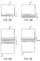
- FIG. 3 shows an impurity concentration profile, representing a case where the n buffer layer 23 having an impurity concentration of 3 ⁇ 10 14 cm -3 and a thickness of 30 ⁇ m and the n + buffer layer 31 having an impurity concentration of 1 ⁇ 10 18 cm -3 are used in combination.
- FIG. 4 shows an impurity concentration profile, representing a case where the n buffer layer 23 is formed by using an OSL (One Side Lap) wafer.
- FIGS. 5A to 5C and 6 show a case in which a wafer including an n buffer layer 23 formed in advance by epitaxial growth is used.
- a wafer 51 includes an n buffer layer 23 formed in advance by epitaxial growth.
- the n buffer layer 23 is, for example, 625 ⁇ m thick.
- a p base layer 14, an n + source region 15, a trench-type gate electrode 16, a gate insulating film 17 and a source electrode 41 are sequentially formed by a known process.
- the rear surface of the buffer layer 23 is lapped.
- the total thickness from the main surface of the base layer 14 to the rear surface of the n buffer layer 23 is, for example, 60 to 80 ⁇ m.
- phosphorus and boron are sequentially ion-injected through the rear surface of the n buffer layer 23.
- a heat treatment such as laser annealing, flash annealing, sintering or diffusion, is performed, thereby forming an n + buffer layer 31 and a p + drain layer 22.
- a drain electrode 42 is formed. As a result, the IGBT shown in FIG. 1 is completed.
- the source electrode 41 may be formed after the n + buffer layer and the drain layer 22 are formed.
- FIGS. 7A to 7C show a case in which an OSL wafer including an n buffer layer 23 is used.
- the step of forming a MOS transistor and the step of forming an n + buffer layer 31 and a drain layer 22 are the same as those in the first manufacturing method.
- an OSL wafer 71 includes an n buffer layer 23 and an n - high resistance layer 21.
- the surface of the n - high resistance layer 21 is lapped in advance so that the wafer has a thickness of, for example, 250 ⁇ m.
- FIG. 7B shows the relationship between the impurity concentration and the thickness in the buffer layer 23 and the n - high resistance layer 21. These layers have the concentrations as mentioned above.
- a p base layer 14, an n + source region 15, a trench-type gate electrode 16, a gate insulating film 17 and a source electrode 41 are sequentially formed by the known process as in the first manufacturing method. Then, the rear surface of the n buffer layer 23 is lapped such that the total thickness is, for example, 60 to 80 ⁇ m. Thereafter, an n + buffer layer 31 and a drain layer 22 are formed in the same manner as in the first manufacturing method.
- the effect of the second manufacturing method is the same as that of the first manufacturing method.
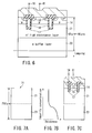
- FIGS. 8A to 8D and 9A to 9D show a third manufacturing method according to the present invention, in which an IGBT having a drain layer doped at a low dose is used. With this method, the thickness after lapping can be controlled with high accuracy.
- a wafer 81 is made of n-type silicon.
- n buffer layer 32 for example, phosphorus is ion-injected into one surface of the wafer 81. Then, a heat treatment is performed, thereby forming the n buffer layer 23, as shown in FIG. 8B. Subsequently, an oxide film 82 is formed on the one surface of the wafer 81.
- the wafer 81 is caused to adhere to a supporting substrate 83.
- the supporting surface 83, as well as the wafer 81, is an n-type silicon wafer. It has an oxide film 84 in one surface portion.
- the oxide film 82 of the wafer 81 and the oxide film 84 of the supporting substrate 83 are faced each other, and joined together by van der Waals force. These oxide films 82 and 84 may have any thickness. Oxide films need not be formed on both the wafer 81 and the supporting substrate 82, but may be formed on only one of them. Thus, the substrate of a SOI structure is formed.
- the other surface of the wafer 81 is lapped.
- the wafer 81 is lapped to a thickness of about, for example, 60 ⁇ m.
- the n - high resistance layer 21 is formed on the n buffer layer 23.
- a trench-type IGBT MOS gate structure 85 is formed in the n - high resistance layer 21 through the same process as in the first and second methods.
- the supporting substrate 83 is lapped and removed.
- the oxide films 82 and 84 are removed by, for example, CDE (Chemical Dry Etching).
- CDE Chemical Dry Etching
- the oxide films 82 and 84 and the silicon wafer can be selectively etched. Therefore, the etching of the oxide films 82 and 84 is stopped at the interface between the n buffer layer 23 and the oxide films 82 and 84.
- the thickness of the wafer 81 can be maintained after the etching. In other words, the lapping error that was inevitable in the conventional device can be eliminated by etching the supporting substrate 83 in the above SOI structure.
- the anode side is processed. More specifically, for example, boron is ion-injected to a surface region of the n buffer layer 23. Then, a heat treatment, such as laser annealing, flash annealing, sintering or diffusion, is performed, thereby forming a p + drain layer 22. Finally, a drain electrode is formed, with the result that the IGBT is completed.
- the SOI structure comprised of the wafer 81 and the supporting substrate 83 is used.
- the wafer 81 is lapped and the MOS gate structure 85 is formed, and thereafter the supporting substrate 83 is removed. Further, the oxide films 82 and 84 are removed by selective etching.
- the third method is advantageous in that the IGBT having designed characteristics can be manufactured.
- FIGS. 10A to 10D and 11A to 11D show a fourth manufacturing method according to the present invention.
- the same parts as those in the third method are identified by the same reference numerals as those used in the description of the third method.
- the fourth manufacturing method is different from the third manufacturing method in the following respect: an n buffer layer and a p + drain layer are formed after the substrate is thinned.
- an oxide film 82 is formed on one surface of a wafer 81 made of n-type silicon.
- the wafer 81 is caused to adhere to a supporting substrate 83.
- the supporting surface 83, as well as the wafer 81, is an n-type silicon wafer. It has an oxide film 84 in one surface portion.
- the oxide film 82 of the wafer 81 and the oxide film 84 of the supporting substrate 83 are faced each other, and joined together by van der Waals force. These oxide films 82 and 84 may have any thickness. Oxide films need not be formed on both the wafer 81 and the supporting substrate 82, but may be formed on only one of them. Thus, the substrate of a SOI structure is formed.
- the other surface of the wafer 81 is lapped.
- the wafer 81 is lapped to a thickness of about, for example, 60 ⁇ m.
- an n - high resistance layer 21 is formed.
- a trench-type IGBT MOS gate structure 85 is formed in the n - high resistance layer 21 of the wafer 81 through the same process as in the first to third methods.
- the supporting substrate 83 is lapped and removed.
- the oxide films 82 and 84 are removed by, for example, CDE.
- the etching is stopped at the interface between the n - high resistance layer 21 and the oxide films 82 and 84.
- the thickness of the wafer 81 can be maintained after the etching.
- the anode side is processed. More specifically, for example, phosphorus is ion-injected to the rear surface of the n - high resistance layer 21, thereby forming an n buffer layer 23.
- boron is ion-injected to a surface region of the n buffer layer 23.
- a heat treatment such as laser annealing, flash annealing, sintering or diffusion, is performed, thereby forming a p + drain layer 22.
- a drain electrode is formed, with the result that the IGBT is completed.
- the effect of the fourth manufacturing method is the same as that of the third manufacturing method. Moreover, since the p + drain layer 22 is formed in a close-to-final step, the fourth method has advantages that the influence of the heat treatment is less and variation in dose or thickness can be prevented.
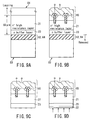
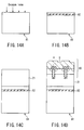
- FIGS. 12A to 12D and 13A and 13B show a fifth manufacturing method according to the present invention.
- the same parts as those in the third method are identified by the same reference numerals as those used in the description of the third method.
- the fifth manufacturing method is different from the fourth manufacturing method in the following respect: impurity ions are injected into a wafer 81 to form an n buffer layer 23 and a p + drain layer 22 before a SOI structure is formed.
- phosphorus (P) to form an n buffer layer 23 is ion-injected into one surface of an n-type silicon wafer 81.
- boron (B) to form a p + drain layer 22 is ion-injected to the wafer 81.
- an oxide film 82 is formed on the one surface of the wafer 81, as shown in
- FIG. 12B is a diagrammatic representation of FIG. 12B.
- the wafer 81 is caused to adhere to a supporting substrate 83.
- the supporting surface 83, as well as the wafer 81, is an n-type silicon wafer. It has an oxide film 84 in one surface portion.
- the oxide film 82 of the wafer 81 and the oxide film 84 of the supporting substrate 83 are faced each other, and joined together by van der Waals force. These oxide films 82 and 84 may have any thickness. Oxide films need not be formed on both the wafer 81 and the supporting substrate 82, but may be formed on only one of them. Thus, the substrate of a SOI structure is formed.
- the other surface of the wafer 81 is lapped, thereby forming an n - high resistance layer 21.
- the wafer 81 is lapped to a thickness of about, for example, 60 ⁇ m.
- a trench-type IGBT MOS gate structure 85 is formed in the n - high resistance layer 21 of the wafer 81 in the same process as in the first to fourth methods.
- the phosphorus and boron ions that have been injected in the wafer 81 are diffused by heat processes.
- an n buffer layer 23 and a p + drain layer 22 are formed.
- the supporting substrate 83 is lapped and removed.
- the oxide films 82 and 84 are removed by, for example, CDE.
- the oxide films 82 and 84 and the silicon wafer can be selectively etched. Therefore, the etching can be stopped at the interface between the n buffer layer 23 and the oxide films 82 and 84.
- the thickness of the wafer 81 can be maintained after the etching. In other words, the lapping error that was inevitable in the conventional device can be eliminated by etching the supporting substrate 83 in the above SOI structure.
- the impurity ions to form the n buffer layer 23 and the p + drain layer 22 are injected into the wafer 81 before the SOI structure is formed. Therefore, since the ions are injected successively, the manufacturing process is simplified. In addition, since the ions are injected to the thick wafer, the process can be eased.
- FIGS. 14A to 14D and 15A and 15B show a sixth manufacturing method according to the present invention.
- the same parts as those in the third method are identified by the same reference numerals as those used in the description of the third method.
- the SOI structure is formed by joining the wafer 81 and the supporting substrate 83.
- the SOI structure is formed by using a substrate of a SIMOX (Separation by IMplanted OXide).
- oxygen is ion-injected into one surface of an n-type silicon wafer 81.
- an oxide film 82 is formed at a depth of several microns from the surface of the wafer 81, as shown in FIG. 14B.
- an n - high resistance layer 21 is formed on the surface of the wafer 81 by, for example, epitaxial growth.
- the epitaxial growth is controlled such that the n - high resistance layer 21 has a thickness of, for example, 60 ⁇ m from the oxide film 82.
- the substrate of the SOI structure is formed.
- a trench-type IGBT MOS gate structure 85 is formed in the n - high resistance layer 21 of the wafer 81 in the same process as in the first to fifth methods.
- the rear surface of the wafer 81 is lapped and removed.
- the oxide film 82 is removed by, for example, CDE.
- the oxide film 82 and the silicon wafer can be selectively etched. Therefore, the thickness of the wafer 81 on the n - high resistance layer 21 side can be maintained after the etching. In other words, the lapping error that was inevitable in the conventional device can be eliminated by etching the wafer 81 in the above SOI structure.
- phosphorus and boron are sequentially ion-injected through the rear surface of the wafer 81, so that an n buffer layer 23 and a p + drain layer 22 are formed.
- the IGBT is manufactured by using a substrate of the SIMOX structure. Since it is unnecessary to use a supporting substrate, the manufacturing cost can be reduced.
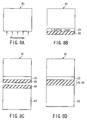
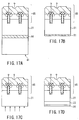
- FIGS. 16A, 16B and 17A to 17D show a seventh manufacturing method according to the present invention.
- the same parts as those in the third method are identified by the same reference numerals as those used in the description of the third method.
- the SOI structure is formed by joining the supporting substrate 83 and the wafer 81.
- the seventh method uses a porous silicon instead.
- a porous silicon layer 91 is formed on one surface of a wafer 81 made of n type silicon, which serves as a supporting substrate.
- an n - high resistance layer 21 is formed on the surface of the porous silicon layer 91 by, for example, epitaxial growth.
- the epitaxial growth is controlled such that the n - high resistance layer 21 has a thickness of, for example, 60 ⁇ m.
- a trench-type IGBT MOS gate structure 85 is formed in the n - high resistance layer 21 in the same process as in the first to sixth methods.
- the n - high resistance layer 21 and the wafer 81 are separated from each other at the porous silicon layer 91. Thereafter, the porous silicon layer 91 is removed by, for example, CDE.
- phosphorus and boron are sequentially ion-injected through the rear surface of the n - high resistance layer 21, so that an n buffer layer 23 and a p + drain layer 22 are formed.
- the porous silicon layer 91 is formed on the wafer 81. After the MOS gate structure 85 is formed in the n - high resistance layer 21 on the porous silicon layer 91, the wafer 81 is separated from the n - high resistance layer 21 at the porous silicon layer 91. Thus, since no lapping process is required, the seventh method has an advantage that the thickness of the n - high resistance layer 21 does not vary.
- the wafer 81 serving as a supporting substrate can be reused after being separated from the n - high resistance layer 21 at the porous silicon layer 91. Therefore, the manufacturing cost can be reduced.
- an n + buffer 31 may be formed between the n buffer layer 23 and the p + drain layer 22 as in the embodiment shown in FIG. 1.
- the oxide films 82 and 84 are used to form a SOI structure.
- any other material for the same purpose so far as that can be selectively etched from silicon.
- the above descriptions of the embodiments refer to a trench-type IGBT as an example.
- the present invention is not limited to this type.
- the present invention can be applied to a planar-type IGBT.
Landscapes
- Thin Film Transistor (AREA)
- Bipolar Transistors (AREA)
Applications Claiming Priority (2)
| Application Number | Priority Date | Filing Date | Title |
|---|---|---|---|
| JP2001054945 | 2001-02-28 | ||
| JP2001054945A JP3764343B2 (ja) | 2001-02-28 | 2001-02-28 | 半導体装置の製造方法 |
Publications (2)
| Publication Number | Publication Date |
|---|---|
| EP1237200A2 true EP1237200A2 (de) | 2002-09-04 |
| EP1237200A3 EP1237200A3 (de) | 2004-06-23 |
Family
ID=18915205
Family Applications (1)
| Application Number | Title | Priority Date | Filing Date |
|---|---|---|---|
| EP02004311A Withdrawn EP1237200A3 (de) | 2001-02-28 | 2002-02-28 | Hochspannungshalbleiteranordnung und Verfahren zur Herstellung |
Country Status (3)
| Country | Link |
|---|---|
| US (1) | US6683343B2 (de) |
| EP (1) | EP1237200A3 (de) |
| JP (1) | JP3764343B2 (de) |
Cited By (5)
| Publication number | Priority date | Publication date | Assignee | Title |
|---|---|---|---|---|
| EP1672698A1 (de) * | 2004-12-16 | 2006-06-21 | ABB Technology AG | Leistungshalbleiter |
| DE102005009000B4 (de) * | 2005-02-28 | 2009-04-02 | Infineon Technologies Austria Ag | Vertikales Halbleiterbauelement vom Grabenstrukturtyp und Herstellungsverfahren |
| EP2045844A1 (de) * | 2007-10-03 | 2009-04-08 | ABB Technology AG | Halbleitermodul |
| DE102004039209B4 (de) * | 2004-08-12 | 2009-04-23 | Infineon Technologies Austria Ag | Verfahren zur Herstellung einer n-dotierten Feldstoppzone in einem Halbleiterkörper und Halbleiterbauelement mit einer Feldstoppzone |
| WO2020229402A1 (en) * | 2019-05-10 | 2020-11-19 | Abb Power Grids Switzerland Ag | A dual base thin wafer power semiconductor device and method for manufacturing the same |
Families Citing this family (45)
| Publication number | Priority date | Publication date | Assignee | Title |
|---|---|---|---|---|
| JP2002305304A (ja) * | 2001-04-05 | 2002-10-18 | Toshiba Corp | 電力用半導体装置 |
| EP1382624A1 (de) | 2002-07-15 | 2004-01-21 | Tosoh Corporation | Katalysator und Verfahren für die Herstellung eines harten Polyurethanschaums |
| JP2004119498A (ja) * | 2002-09-24 | 2004-04-15 | Fuji Electric Device Technology Co Ltd | 半導体装置の製造方法 |
| US20060049464A1 (en) | 2004-09-03 | 2006-03-09 | Rao G R Mohan | Semiconductor devices with graded dopant regions |
| TWI401739B (zh) * | 2004-10-21 | 2013-07-11 | 富士軟片迪瑪提斯股份有限公司 | 蝕刻犧牲材 |
| JP2006173297A (ja) * | 2004-12-15 | 2006-06-29 | Denso Corp | Igbt |
| JP5135666B2 (ja) * | 2005-04-14 | 2013-02-06 | 株式会社日立製作所 | 電力変換装置 |
| US20070034941A1 (en) * | 2005-08-15 | 2007-02-15 | International Rectifier Corp. | Deep N diffusion for trench IGBT |
| JP5017850B2 (ja) * | 2005-11-30 | 2012-09-05 | 株式会社日立製作所 | 電力用半導体装置およびそれを用いた電力変換装置 |
| US20070181927A1 (en) * | 2006-02-03 | 2007-08-09 | Yedinak Joseph A | Charge balance insulated gate bipolar transistor |
| JP2008021981A (ja) | 2006-06-16 | 2008-01-31 | Toshiba Corp | 絶縁ゲートバイポーラトランジスタ及びその製造方法 |
| DE102007003812B4 (de) * | 2007-01-25 | 2011-11-17 | Infineon Technologies Ag | Halbleiterbauelement mit Trench-Gate und Verfahren zur Herstellung |
| US7638839B2 (en) * | 2007-03-09 | 2009-12-29 | Hitachi, Ltd. | Power semiconductor device and power conversion device using the same |
| JP5407126B2 (ja) * | 2007-08-30 | 2014-02-05 | 信越半導体株式会社 | 半導体基板の製造方法 |
| CN101983431B (zh) | 2008-03-31 | 2014-02-19 | 三菱电机株式会社 | 半导体装置 |
| JP5609087B2 (ja) | 2009-12-04 | 2014-10-22 | 富士電機株式会社 | 内燃機関点火装置用半導体装置 |
| US9685523B2 (en) * | 2014-12-17 | 2017-06-20 | Alpha And Omega Semiconductor Incorporated | Diode structures with controlled injection efficiency for fast switching |
| JP5874723B2 (ja) | 2011-05-18 | 2016-03-02 | 富士電機株式会社 | 半導体装置および半導体装置の製造方法 |
| JP6037495B2 (ja) * | 2011-10-17 | 2016-12-07 | ローム株式会社 | 半導体装置およびその製造方法 |
| CN103094324B (zh) * | 2011-11-08 | 2016-03-23 | 无锡华润上华半导体有限公司 | 沟槽型绝缘栅双极型晶体管及其制备方法 |
| US9349847B2 (en) | 2011-12-15 | 2016-05-24 | Hitachi, Ltd. | Semiconductor device and power converter |
| WO2013141181A1 (ja) * | 2012-03-23 | 2013-09-26 | 富士電機株式会社 | 半導体装置および半導体装置の製造方法 |
| CN104054178B (zh) | 2012-03-30 | 2017-09-08 | 富士电机株式会社 | 半导体装置的制造方法 |
| KR101876579B1 (ko) * | 2012-09-13 | 2018-07-10 | 매그나칩 반도체 유한회사 | 전력용 반도체 소자 및 그 소자의 제조 방법 |
| US8878238B2 (en) * | 2012-10-01 | 2014-11-04 | Pakal Technologies Llc | MCT device with base-width-determined latching and non-latching states |
| CN103871852B (zh) * | 2012-12-14 | 2018-01-30 | 中国科学院微电子研究所 | 一种带fs层的pt型功率器件的制作方法 |
| US20160005843A1 (en) * | 2013-02-12 | 2016-01-07 | Toyota Jidosha Kabushiki Kaisha | Semiconductor device and manufacturing method thereof |
| CN104112663A (zh) * | 2013-04-18 | 2014-10-22 | 比亚迪股份有限公司 | 一种半导体结构及其形成方法 |
| JP6271155B2 (ja) | 2013-05-21 | 2018-01-31 | 株式会社東芝 | 半導体装置 |
| JP6311723B2 (ja) | 2013-12-16 | 2018-04-18 | 富士電機株式会社 | 半導体装置および半導体装置の製造方法 |
| JP2015201476A (ja) * | 2014-04-04 | 2015-11-12 | 三菱電機株式会社 | 半導体装置およびその製造方法 |
| KR101955055B1 (ko) | 2014-11-28 | 2019-03-07 | 매그나칩 반도체 유한회사 | 전력용 반도체 소자 및 그 소자의 제조 방법 |
| US9391135B1 (en) | 2015-03-23 | 2016-07-12 | Semiconductor Components Industries, Llc | Semiconductor device |
| US20180151709A1 (en) * | 2015-06-01 | 2018-05-31 | Hitachi, Ltd. | Semiconductor device, substrate and electrical power conversion device |
| US9991338B2 (en) | 2015-09-17 | 2018-06-05 | Semiconductor Components Industries, Llc | Electronic device including a conductive structure surrounded by an insulating structure |
| US10411093B2 (en) | 2015-12-28 | 2019-09-10 | Mitsubishi Electric Corporation | Semiconductor device and method for manufacturing semiconductor device |
| US9768285B1 (en) | 2016-03-16 | 2017-09-19 | Semiconductor Components Industries, Llc | Semiconductor device and method of manufacture |
| US10497602B2 (en) | 2016-08-01 | 2019-12-03 | Semiconductor Components Industries, Llc | Process of forming an electronic device including forming an electronic component and removing a portion of a substrate |
| JP6820811B2 (ja) * | 2017-08-08 | 2021-01-27 | 三菱電機株式会社 | 半導体装置および電力変換装置 |
| US20200105874A1 (en) * | 2018-10-01 | 2020-04-02 | Ipower Semiconductor | Back side dopant activation in field stop igbt |
| CN109712885A (zh) * | 2018-12-17 | 2019-05-03 | 成都森未科技有限公司 | 一种半导体器件缓冲层制造方法 |
| US20210384346A1 (en) * | 2020-06-03 | 2021-12-09 | Nami MOS CO., LTD. | Shielded gate trench mosfet having super junction surrounding lower portion of trenched gates |
| DE112021000205T5 (de) | 2020-07-15 | 2022-08-18 | Fuji Electric Co., Ltd. | Halbleitervorrichtung |
| CN116978937A (zh) | 2021-02-07 | 2023-10-31 | 华为技术有限公司 | 半导体器件及相关模块、电路、制备方法 |
| DE102021115825B4 (de) * | 2021-06-18 | 2026-04-23 | Infineon Technologies Ag | Feldstoppgebiet enthaltende halbleitervorrichtung |
Family Cites Families (21)
| Publication number | Priority date | Publication date | Assignee | Title |
|---|---|---|---|---|
| JP2918399B2 (ja) * | 1992-08-05 | 1999-07-12 | 三菱電機株式会社 | 半導体装置およびその製造方法 |
| JPH06268226A (ja) | 1993-03-10 | 1994-09-22 | Fuji Electric Co Ltd | 絶縁ゲート型バイポーラトランジスタ |
| US5466951A (en) | 1993-12-08 | 1995-11-14 | Siemens Aktiengesellschaft | Controllable power semiconductor element with buffer zone and method for the manufacture thereof |
| US5751024A (en) * | 1995-03-14 | 1998-05-12 | Mitsubishi Denki Kabushiki Kaisha | Insulated gate semiconductor device |
| US6001678A (en) * | 1995-03-14 | 1999-12-14 | Mitsubishi Denki Kabushiki Kaisha | Insulated gate semiconductor device |
| JPH08288503A (ja) * | 1995-04-11 | 1996-11-01 | Rohm Co Ltd | プレーナ型高耐圧縦型素子を有する半導体装置およびその製造方法 |
| US5843796A (en) * | 1995-09-11 | 1998-12-01 | Delco Electronics Corporation | Method of making an insulated gate bipolar transistor with high-energy P+ im |
| US5679966A (en) * | 1995-10-05 | 1997-10-21 | North Carolina State University | Depleted base transistor with high forward voltage blocking capability |
| JP3378135B2 (ja) * | 1996-02-02 | 2003-02-17 | 三菱電機株式会社 | 半導体装置とその製造方法 |
| JP3426928B2 (ja) * | 1996-09-18 | 2003-07-14 | 株式会社東芝 | 電力用半導体装置 |
| DE19640307C2 (de) * | 1996-09-30 | 2000-10-12 | Siemens Ag | Durch Feldeffekt steuerbares Halbleiterbauelement |
| JPH10189956A (ja) | 1996-12-25 | 1998-07-21 | Hitachi Ltd | 半導体装置 |
| GB2321337B (en) * | 1997-01-21 | 2001-11-07 | Plessey Semiconductors Ltd | Improvements in or relating to semiconductor devices |
| DE19811297B4 (de) * | 1997-03-17 | 2009-03-19 | Fuji Electric Co., Ltd., Kawasaki | MOS-Halbleitervorrichtung mit hoher Durchbruchspannung |
| JP3431467B2 (ja) * | 1997-09-17 | 2003-07-28 | 株式会社東芝 | 高耐圧半導体装置 |
| JP3523056B2 (ja) | 1998-03-23 | 2004-04-26 | 株式会社東芝 | 半導体装置 |
| KR100295063B1 (ko) * | 1998-06-30 | 2001-08-07 | 김덕중 | 트렌치게이트구조의전력반도체장치및그제조방법 |
| DE19829614B4 (de) * | 1998-07-02 | 2004-09-23 | Semikron Elektronik Gmbh | Verfahren zur Herstellung eines Leistungshalbleiterbauelementes |
| KR100275756B1 (ko) * | 1998-08-27 | 2000-12-15 | 김덕중 | 트렌치 절연 게이트 바이폴라 트랜지스터 |
| JP2000260778A (ja) | 1999-03-11 | 2000-09-22 | Toshiba Corp | 半導体装置およびその製造方法 |
| JP4088011B2 (ja) * | 2000-02-16 | 2008-05-21 | 株式会社東芝 | 半導体装置及びその製造方法 |
-
2001
- 2001-02-28 JP JP2001054945A patent/JP3764343B2/ja not_active Expired - Fee Related
-
2002
- 2002-02-28 US US10/084,051 patent/US6683343B2/en not_active Expired - Fee Related
- 2002-02-28 EP EP02004311A patent/EP1237200A3/de not_active Withdrawn
Cited By (10)
| Publication number | Priority date | Publication date | Assignee | Title |
|---|---|---|---|---|
| DE102004039209B4 (de) * | 2004-08-12 | 2009-04-23 | Infineon Technologies Austria Ag | Verfahren zur Herstellung einer n-dotierten Feldstoppzone in einem Halbleiterkörper und Halbleiterbauelement mit einer Feldstoppzone |
| EP1672698A1 (de) * | 2004-12-16 | 2006-06-21 | ABB Technology AG | Leistungshalbleiter |
| WO2006063478A1 (de) * | 2004-12-16 | 2006-06-22 | Abb Technology Ag | Leistungshalbleiter |
| US8501586B2 (en) | 2004-12-16 | 2013-08-06 | Abb Technology Ag | Power semiconductor |
| DE102005009000B4 (de) * | 2005-02-28 | 2009-04-02 | Infineon Technologies Austria Ag | Vertikales Halbleiterbauelement vom Grabenstrukturtyp und Herstellungsverfahren |
| US7652325B2 (en) | 2005-02-28 | 2010-01-26 | Infineon Technologies Austria Ag | Field effect controllable semiconductor component with improved inverse diode and production methods therefor |
| EP2045844A1 (de) * | 2007-10-03 | 2009-04-08 | ABB Technology AG | Halbleitermodul |
| WO2009043870A1 (en) * | 2007-10-03 | 2009-04-09 | Abb Technology Ag | Semiconductor module |
| US8450793B2 (en) | 2007-10-03 | 2013-05-28 | Abb Technology Ag | Semiconductor module |
| WO2020229402A1 (en) * | 2019-05-10 | 2020-11-19 | Abb Power Grids Switzerland Ag | A dual base thin wafer power semiconductor device and method for manufacturing the same |
Also Published As
| Publication number | Publication date |
|---|---|
| US20020117712A1 (en) | 2002-08-29 |
| US6683343B2 (en) | 2004-01-27 |
| JP2002261282A (ja) | 2002-09-13 |
| EP1237200A3 (de) | 2004-06-23 |
| JP3764343B2 (ja) | 2006-04-05 |
Similar Documents
| Publication | Publication Date | Title |
|---|---|---|
| US6683343B2 (en) | High voltage semiconductor device having two buffer layer | |
| JP3906076B2 (ja) | 半導体装置 | |
| KR100328133B1 (ko) | 전계효과에의해제어가능한수직반도체소자 | |
| KR0134794B1 (ko) | 전도도 변조형 반도체 장치 및 그 제조방법 | |
| US5541122A (en) | Method of fabricating an insulated-gate bipolar transistor | |
| JPH05347413A (ja) | 半導体装置の製造方法 | |
| US5506153A (en) | Method for manufacture of a controllable power semiconductor element with buffer zone | |
| US11810970B2 (en) | Semiconductor device and a manufacturing method of semiconductor device | |
| KR950014279B1 (ko) | 반도체 장치 및 그 제조 방법 | |
| US6524894B1 (en) | Semiconductor device for use in power-switching device and method of manufacturing the same | |
| JP2000269487A (ja) | 半導体装置及びその製造方法 | |
| JP4746927B2 (ja) | 半導体装置の製造方法 | |
| JP2002261281A (ja) | 絶縁ゲートバイポーラトランジスタの製造方法 | |
| JP4372082B2 (ja) | 半導体装置とその製造方法 | |
| JP4676708B2 (ja) | 半導体装置の製造方法 | |
| JP2005051111A (ja) | メサ型半導体装置 | |
| JP5248741B2 (ja) | 逆阻止型絶縁ゲート形半導体装置およびその製造方法 | |
| KR100689208B1 (ko) | 반도체 장치 및 반도체 장치의 제조 방법 | |
| US11335771B2 (en) | Semiconductor device | |
| JP2006080269A (ja) | 高耐圧半導体装置およびその製造方法 | |
| JP2006140309A (ja) | 半導体装置の製造方法 | |
| JPH04206933A (ja) | 半導体装置 | |
| JPH0982955A (ja) | 半導体装置の製法 | |
| KR20080068658A (ko) | Soi 트렌치 횡형 igbt | |
| JP4349798B2 (ja) | 半導体装置の製造方法 |
Legal Events
| Date | Code | Title | Description |
|---|---|---|---|
| PUAI | Public reference made under article 153(3) epc to a published international application that has entered the european phase |
Free format text: ORIGINAL CODE: 0009012 |
|
| 17P | Request for examination filed |
Effective date: 20020228 |
|
| AK | Designated contracting states |
Kind code of ref document: A2 Designated state(s): AT BE CH CY DE DK ES FI FR GB GR IE IT LI LU MC NL PT SE TR |
|
| AX | Request for extension of the european patent |
Free format text: AL;LT;LV;MK;RO;SI |
|
| PUAL | Search report despatched |
Free format text: ORIGINAL CODE: 0009013 |
|
| RIC1 | Information provided on ipc code assigned before grant |
Ipc: 7H 01L 21/331 B Ipc: 7H 01L 29/739 B Ipc: 7H 01L 29/08 A |
|
| AK | Designated contracting states |
Kind code of ref document: A3 Designated state(s): AT BE CH CY DE DK ES FI FR GB GR IE IT LI LU MC NL PT SE TR |
|
| AX | Request for extension of the european patent |
Extension state: AL LT LV MK RO SI |
|
| AKX | Designation fees paid |
Designated state(s): CH DE FR IT LI |
|
| 17Q | First examination report despatched |
Effective date: 20050419 |
|
| STAA | Information on the status of an ep patent application or granted ep patent |
Free format text: STATUS: THE APPLICATION IS DEEMED TO BE WITHDRAWN |
|
| 18D | Application deemed to be withdrawn |
Effective date: 20100126 |