EP1128425A1 - Corps fritté en nitrure d'aluminium, article ayant un metal encastré, materiau électronique fonctionnel et mandrin de serrage électrostatique - Google Patents
Corps fritté en nitrure d'aluminium, article ayant un metal encastré, materiau électronique fonctionnel et mandrin de serrage électrostatique Download PDFInfo
- Publication number
- EP1128425A1 EP1128425A1 EP01103195A EP01103195A EP1128425A1 EP 1128425 A1 EP1128425 A1 EP 1128425A1 EP 01103195 A EP01103195 A EP 01103195A EP 01103195 A EP01103195 A EP 01103195A EP 1128425 A1 EP1128425 A1 EP 1128425A1
- Authority
- EP
- European Patent Office
- Prior art keywords
- sintered body
- aluminum nitride
- rare earth
- ppm
- crystal grains
- Prior art date
- Legal status (The legal status is an assumption and is not a legal conclusion. Google has not performed a legal analysis and makes no representation as to the accuracy of the status listed.)
- Granted
Links
Images


Classifications
-
- C—CHEMISTRY; METALLURGY
- C04—CEMENTS; CONCRETE; ARTIFICIAL STONE; CERAMICS; REFRACTORIES
- C04B—LIME, MAGNESIA; SLAG; CEMENTS; COMPOSITIONS THEREOF, e.g. MORTARS, CONCRETE OR LIKE BUILDING MATERIALS; ARTIFICIAL STONE; CERAMICS; REFRACTORIES; TREATMENT OF NATURAL STONE
- C04B35/00—Shaped ceramic products characterised by their composition; Ceramics compositions; Processing powders of inorganic compounds preparatory to the manufacturing of ceramic products
- C04B35/515—Shaped ceramic products characterised by their composition; Ceramics compositions; Processing powders of inorganic compounds preparatory to the manufacturing of ceramic products based on non-oxide ceramics
- C04B35/58—Shaped ceramic products characterised by their composition; Ceramics compositions; Processing powders of inorganic compounds preparatory to the manufacturing of ceramic products based on non-oxide ceramics based on borides, nitrides, i.e. nitrides, oxynitrides, carbonitrides or oxycarbonitrides or silicides
- C04B35/581—Shaped ceramic products characterised by their composition; Ceramics compositions; Processing powders of inorganic compounds preparatory to the manufacturing of ceramic products based on non-oxide ceramics based on borides, nitrides, i.e. nitrides, oxynitrides, carbonitrides or oxycarbonitrides or silicides based on aluminium nitride
-
- B—PERFORMING OPERATIONS; TRANSPORTING
- B23—MACHINE TOOLS; METAL-WORKING NOT OTHERWISE PROVIDED FOR
- B23Q—DETAILS, COMPONENTS, OR ACCESSORIES FOR MACHINE TOOLS, e.g. ARRANGEMENTS FOR COPYING OR CONTROLLING; MACHINE TOOLS IN GENERAL CHARACTERISED BY THE CONSTRUCTION OF PARTICULAR DETAILS OR COMPONENTS; COMBINATIONS OR ASSOCIATIONS OF METAL-WORKING MACHINES, NOT DIRECTED TO A PARTICULAR RESULT
- B23Q3/00—Devices holding, supporting, or positioning work or tools, of a kind normally removable from the machine
- B23Q3/15—Devices for holding work using magnetic or electric force acting directly on the work
-
- H—ELECTRICITY
- H01—ELECTRIC ELEMENTS
- H01L—SEMICONDUCTOR DEVICES NOT COVERED BY CLASS H10
- H01L21/00—Processes or apparatus adapted for the manufacture or treatment of semiconductor or solid state devices or of parts thereof
- H01L21/67—Apparatus specially adapted for handling semiconductor or electric solid state devices during manufacture or treatment thereof; Apparatus specially adapted for handling wafers during manufacture or treatment of semiconductor or electric solid state devices or components ; Apparatus not specifically provided for elsewhere
- H01L21/68—Apparatus specially adapted for handling semiconductor or electric solid state devices during manufacture or treatment thereof; Apparatus specially adapted for handling wafers during manufacture or treatment of semiconductor or electric solid state devices or components ; Apparatus not specifically provided for elsewhere for positioning, orientation or alignment
-
- H—ELECTRICITY
- H01—ELECTRIC ELEMENTS
- H01L—SEMICONDUCTOR DEVICES NOT COVERED BY CLASS H10
- H01L21/00—Processes or apparatus adapted for the manufacture or treatment of semiconductor or solid state devices or of parts thereof
- H01L21/67—Apparatus specially adapted for handling semiconductor or electric solid state devices during manufacture or treatment thereof; Apparatus specially adapted for handling wafers during manufacture or treatment of semiconductor or electric solid state devices or components ; Apparatus not specifically provided for elsewhere
- H01L21/683—Apparatus specially adapted for handling semiconductor or electric solid state devices during manufacture or treatment thereof; Apparatus specially adapted for handling wafers during manufacture or treatment of semiconductor or electric solid state devices or components ; Apparatus not specifically provided for elsewhere for supporting or gripping
- H01L21/6831—Apparatus specially adapted for handling semiconductor or electric solid state devices during manufacture or treatment thereof; Apparatus specially adapted for handling wafers during manufacture or treatment of semiconductor or electric solid state devices or components ; Apparatus not specifically provided for elsewhere for supporting or gripping using electrostatic chucks
- H01L21/6833—Details of electrostatic chucks
-
- Y—GENERAL TAGGING OF NEW TECHNOLOGICAL DEVELOPMENTS; GENERAL TAGGING OF CROSS-SECTIONAL TECHNOLOGIES SPANNING OVER SEVERAL SECTIONS OF THE IPC; TECHNICAL SUBJECTS COVERED BY FORMER USPC CROSS-REFERENCE ART COLLECTIONS [XRACs] AND DIGESTS
- Y10—TECHNICAL SUBJECTS COVERED BY FORMER USPC
- Y10T—TECHNICAL SUBJECTS COVERED BY FORMER US CLASSIFICATION
- Y10T279/00—Chucks or sockets
- Y10T279/23—Chucks or sockets with magnetic or electrostatic means
Definitions
- the present invention relates to a novel aluminum nitride sintered body having a high purity and a low volume resistivity, and metal embedded articles, electronic functional materials and electrostatic chucks utilizing this aluminum nitride sintered body.
- electrostatic chucks are used for attracting and holding the semiconductor wafer.
- dense ceramics have been drawing attention.
- halogenous corrosive gases such as ClF 3 and the like are frequently used as etching gases or cleaning gases.
- the substrate of the electrostatic chuck is desired to have a high thermal conductivity.
- a dense aluminum nitride has a high corrosive resistance against halogenous corrosive gases as mentioned above.
- aluminum nitride is a high thermal conductive material and its volume resistivity is not less than 10 14 ⁇ cm at room temperature.
- aluminum nitride has a high thermal shock resistance. Therefore, it is accounted preferable to form a substrate of an electrostatic chuck for semiconductor manufacturing apparatuses of an aluminum nitride sintered body.
- ceramics starting materials containing alumina as a main component are fired in a reducing atmosphere to produce dielectric ceramics for electrostatic chucks.
- the ceramic starting material is made to contain an alkali earth metal and a transition metal in amounts as oxide of 1-6 % and 0.5-6 %, by weight, respectively.
- it is intended to increase the dielectric constant, concurrently decreasing the volume resistivity to 10 12 - 10 18 ⁇ ⁇ cm, by incorporating TiO 2 with the alumina ceramics, thereby to obtain a high attracting power.
- the present inventors have restudied the aluminum nitride sintered bodies per se.
- an object of the present invention to provide a novel aluminum nitride sintered body having a high purity and a low volume resistivity.
- an aluminum nitride sintered body characterized by comprising rare earth element(s) in a total amount (as oxide thereof) of 150 ppm - 0.5 %, by weight, and at least one metal impurity except rare earth elements in a total amount of not more than 900 ppm, and having a main peak within a wavelength region of from 350 nm - 370 nm in a spectrum obtained by a cathode luminescence method.
- an aluminum nitride sintered body characterized by comprising rare earth element(s) in a total amount (as oxide thereof) of 150 ppm - 0.5 %, by weight, at least one metal impurity except rare earth elements in a total amount of not more than 900 ppm, and constituent aluminum nitride crystal grains having an oxygen concentration of 0.50% ⁇ 2.00 %, by weight, measured by an electron probe X-ray microanalyzer.
- an aluminum nitride sintered body characterized by comprising rare earth element(s) in a total amount (as oxide thereof) of 150 ppm - 0.5 %, by weight, and at least one metal impurity except rare earth elements in a total amount of not more than 900 ppm, and having a g-value of an unpaired electron of not more than 2.000 in a spectrum of the aluminum nitride sintered body obtained by an electron spin resonance method.
- an aluminum nitride sintered body characterized by comprising rare earth element(s) in a total amount (as oxide thereof) of 150 ppm - 0.5 %, by weight, and at least one metal impurity except rare earth elements in a total amount of not more than 900 ppm, and having a spin amount obtained from a spectrum measured by electron spin resonance method of at least 1 x 10 13 spins per unit mg of aluminum.
- an aluminum nitride sintered body characterized by comprising rare earth element(s) in a total amount (as oxide thereof) of 150 ppm - 0.5 %, by weight, at least one metal impurity except rare earth elements in a total amount of not more than 900 ppm, and constituent aluminum nitride crystal grains having an average grain diameter of at least 3.0 ⁇ m, and said aluminum nitride sintered body having a volume resistivity of 1.0 x 10 6 -1.0 ⁇ 10 12 ⁇ cm.
- a metal embedded article comprising one of the aforesaid aluminum nitride sintered bodies and a metal member embedded therein.
- This aspect further provides an electronic functional material comprising one of the aforesaid aluminum nitride sintered bodies.
- an electrostatic chuck having an attracting surface for attracting and holding a semiconductor, which comprises a substrate comprising one of the aforesaid aluminum nitride sintered bodies, a plate-type electrode embedded therein, and a power source for supplying the plate-type electrode with a direct current power.
- the present inventors in the course of manufacture of an aluminum sintered body containing not more than 900 ppm of at least one metal impurity other than rare earth elements, have surprisingly succeeded in providing an aluminum nitride sintered body with a volume resistivity of not more than 1 x 10 12 ⁇ cm by adjusting the content of the rare earth elements (as oxides thereof) in the sintered body to not more than 0.5 % by weight, and preferably making the sintering to proceed so that constituent aluminum nitride crystal grains may have an average grain diameter of at least 3.0 ⁇ m.
- the reason for such a result is not clear, but it can be conjectured as follows:
- the resistance of aluminum nitride sintered bodies can be calculated as a resistance of a circuit formed by connecting aluminum nitride crystal grain resistances with grain boundary resistances in series and parallel.
- the present inventors have accelerated densification of a sintered body, by employing aluminum nitride particles with high purity, admixing a small amount of a rare earth element therewith, and applying a high pressure by means of hot pressing or the like.
- the rare earth element compound is admixed in an amount of more than 0.5 % by weight, oxygen existing in the starting particles diffuses towards the outside of the particles during firing.
- the oxygen is made to remain in aluminum nitride crystal grains in the state of solid solution. This oxygen in the crystal grains replaces nitrogen atoms in AlN, to form a donor level in a band gap, with the consequence that the electron conductivity in the grains is improved.
- the oxygen solid-solution in aluminum nitride crystal grains is essential for decreasing the resistance of each crystal grain.
- rare earth elements such as yttrium or the like have been incorporated, as a sintering assistant, with aluminum nitride sintered bodies in an amount as oxide thereof of several percent by weight (Japanese Patent Publication No. 63-46032). If this amount is positively decreased, a dense body becomes hardly obtainable in normal pressure sintering.
- Japanese Patent Publication No. 63-46032 Japanese Patent Publication No. 63-46032
- a study has been conducted to improve a thermal conductivity of aluminum nitride sintered bodies by increasing the amount of these sintering assistants to be added. That is to say, it has been a common sense to add about several % by weight of a sintering assistant in order to decrease porosity and increase thermal conductivity of aluminum nitride sintered bodies.
- the starting powder of aluminum nitrides contains oxygen within the particles thereof.
- the oxygen existing in the inside of each particle diffuses towards the outside of the particles by virtue of an action of the sintering assistant during sintering. It has been assumed that the thermal conductivity is more improved with progressing process of discharging the oxygen from the aluminum nitride particles.
- the oxygen atoms are a kind of impurities which remain in the aluminum nitride crystal grains even after sintering. Accordingly, a study to decrease the amount of oxygen remaining in the grains has been conducted in order to improve the thermal conductivity of sintered bodies. From another point of view, a study for utilizing aluminum nitride sintered bodies as a material having a volume resistivity in the region of semiconductors has not been heretofore conducted.
- the amount of the oxygen remaining in grains after pressure sintering is controlled by adjusting the amount of the rare earth element compound blended and increasing the pressure during sintering, with the consequence that the oxygen is made to remain as a donor for decreasing the resistance of each crystal grain. It is an utterly novel concept that the oxygen remaining in crystal grains after sintering is used as a donor, in order to decrease the volume resistivity of aluminum nitride sintered bodies to the same level as semiconductors.
- the content of the rare earth element(s) in aluminum nitride sintered bodies is necessary to be not more than 0.5 % by weight as oxide thereof. If it exceeds 0.5 % by weight, the oxygen existing in crystal grains diffuses toward the outside of the grains during sintering. If the oxygen is thus purged out and the interior of the grains is purified, the thermal conductivity is increased by virtue of decrease of phonon scattering with decreasing oxygen, but the resistance of each grain is also increased. Further, rare earth elements remaining at boundaries and triple points of each aluminum nitride crystal grain form an intergranular phase. This intergranular phase disorders the crystal lattice near the grain boundary of each aluminum nitride crystal grain adjacent to others, and loosens adhesion between crystal grains.
- the volume resistivity of the sintered bodies can be more lowered by decreasing the content of the rare earth elements to not more than 0.1 % by weight.
- the content of the rare earth elements in the sintered body is made to be not less than 150 ppm. It has been found that if it is made to be not less than 300 ppm, the decrease of the volume resistivity becomes particularly noticeable. From this point of view, the content of the rare earth elements in the sintered body is more preferred to be not less than 300 ppm.
- alkaline metals and transition metals which are regarded as impurities in these processes are not preferred. Further, it is considered that metal impurities except rare earth elements are present inside the grains or at grain boundaries and function to increase an in-grain resistance or grain boundary resistance.
- the content of metal impurities except rare earth elements must be restricted to not more than 900 ppm. If it exceeds 900 ppm, the tendency to increase the volume resistivity of the sintered body is shown as conceived. Since these metals are included as impurities, it is preferred to be as small an amount as possible. Accordingly, the amount of the metal impurities except rare earth elements is preferred to be not more than 500 ppm, more preferably not more than 100 ppm, including 0 ppm to below a detectable limit.
- the average grain diameter of the aluminum nitride crystal grains in the sintered bodies is preferred to be not less than 3.0 ⁇ m, more preferably not less than 4.0 ⁇ m, and most preferably not less than 5.0 ⁇ m.
- the resistance of the crystal grain boundary is larger than that in the crystal grains, for example, in the case where the sintering temperature is increased to grow crystals, a tendency to decrease volume resistivity thereof is shown. It is important to decrease the number of the grain boundaries per the number of the grains, in order to decrease the volume resistivity of the sintered body. Therefore, if the crystal grains have grown to have an average grain diameter only up to less than 3.0 ⁇ m, since the frequency of the grain boundaries per conduction path increases, the resistivity of the sintered body also increases.
- the average diameter of the aluminum nitride crystal grains there is no particular upper limit in the average diameter of the aluminum nitride crystal grains, it is generally preferred to be not more than 20 ⁇ m.
- the aluminum sintered bodies are preferred to have a relative density of not less than 98.5 %, whereby the volume resistivity of the sintered bodies is further decreased. From this point of view, the relative density of the sintered body is preferred to be not less than 99.0 %, more preferably not less than 99.6 %.
- the aluminum nitride sintered bodies are required to be extremely densified, and at the same time, the amount of the rare earth elements added is decreased to such an amount that the rare earth elements substantially may not act as a sintering assistant.
- the amount of other metal elements to be added which is functionable to promote sintering is required to be decreased to the utmost as mentioned above. Under such a condition, generally only a relative density of not more than 90 % can be obtained by means of normal pressure sintering.
- the aluminum sintered bodies according to the present invention it is necessary to employ a press sintering process such as a hot press process and a hot isostatic press process, whereby the aluminum nitride sintered bodies can be densified without requiring any sintering assistant.
- a press sintering process such as a hot press process and a hot isostatic press process
- one of the principal points of the present invention is that a mechanical pressure is also applied during firing.
- the hot press process has been understood as a process for applying a mechanical pressure for promoting densification of sintered bodies.
- the thus obtained aluminum nitride sintered bodies according to the present invention surprisingly can have a volume resistivity in the range of 1 x 10 12 -1 x 10 6 ⁇ cm, particularly not more than 1 x 10 11 ⁇ cm, and more particularly not more than 1 x 10 10 ⁇ cm.
- a range of the volume resistivity belongs just in the region for semiconductors.
- the present invention in highly pure aluminum nitride sintered bodies including very small amounts of metal impurities and rare earth elements, first provides a sintered body having a volume resistivity of semiconductor region. In this respect, the present invention is epoch-making.
- the aluminum nitride sintered bodies have hitherto been studied as an electrically insulating material with a high thermal conductivity. Furthermore, an attempt has been made to decrease the resistance by doping aluminum nitride sintered bodies with an electric conductor or semiconductor. However, a study has not been conducted to decrease the resistance of the aluminum nitride crystal grains per se, like the present invention.
- the present inventors have further investigated boundaries of each crystal grains, and have searched into the reason for the drastic decrease of the volume resistivity of the sintered body.
- the volume resistivity of the sintered body was not so decreased as the case of the present invention, and rare earth elements did not form solid- solution in the crystal grains, so that it is conjectured that if a very small amount of rare earth elements existed in the boundaries of adjacent crystal grains, the resistance at the crystal grain boundaries could be decreased.
- rare earth elements substantially do not exist within the aluminum nitride crystal grains but are present in the boundary of two aluminum nitride crystal grains adjacent to one another.
- the phrase "rare earth elements substantially do not exist in crystal grains" should be understood to mean that there is shown no peak corresponding to rare earth elements by means of EDS (Energy Dispersive X-ray Spectrometer).
- the rare earth elements exist in the grain boundary of adjacent two aluminum nitride crystal grains but do not form a crystalline phase, and are present in the grain boundary between crystal grains on an atomic level. And it has been found that in the grain boundary of adjacent two aluminum nitride crystal grains, the disordered portion of the crystal lattices composing each aluminum nitride crystal grain can hardly been observed, and that the width of this portion is not more than 5 nm, particularly not more than 1 nm. In some measured samples, such a disorder of the crystal lattices at interfaces of the grains substantially could not be observed. It is conjectured that the resistance between crystal grains is extremely decreased, because of such a specific microstructure at the grain boundary of the crystal grains.
- the present inventors have investigated the triple point (triple point formed by three aluminum nitride crystal grains) in the aluminum nitride sintered bodies, and found that the crystalline phase at the triple point substantially does not contain rare earth elements. From this result, it is conjectured that the rare earth elements exist, as an extremely thin amorphous phase, near the surface or on the surface of each aluminum nitride crystal grain. Even at the triple point, it has been found that rare earth elements exist only near the surface or on the surface of the crystal grains.
- the difference between a total oxygen content in an aluminum nitride sintered body and an oxygen content in the assumed oxides of rare earth elements is preferred to be not less than 0.5 % by weight.
- This difference represents the content of the oxygen remaining in the aluminum nitride crystal grains.
- the present inventors have taken spectra by means of an electron spin resonance method (ESR method) with respect of each sample of the aluminum nitride sintered bodes having a low volume resistivity according to the invention, in order to study the constitution of the defect structure of inside the crystalline phase and at the grain boundary.
- ESR method electron spin resonance method
- the g-value of the unpaired electrons of aluminum varies corresponding to a crystal field where the unpaired electrons exist. This g-value is 2.0000 theoretically in a free electron, and 2.002316 after a relativistic correction.
- the Al atom and N atom in the aluminum nitride crystalline phase have a wurtzite structure with four coordinations. Therefore, an sp 3 hybridized orbit is constructed by one aluminum atom and three nitrogen atoms. It is possible to know, from the g-value of each sample, what crystal coordination that unpaired electrons in the lattice defects exist in or what kind of elements exist around the unpaired electrons.
- the g-value of the unpaired electrons of the aluminum in a spectrum by means of ESR method is not more than 2.000.
- the spin amount per unit mg of aluminum obtained from a spectrum by means of ESR method is not less than 1 x 10 13 spin.
- the measuring method was according to the method described in Hiroaki Ohya and Jun Yamauchi: "Electron Spin Resonance” published by Kodansha Co., Ltd. That is, the absorption intensity in ESR spectra is proportional to the percentage of unpaired electrons in the aluminum nitride crystal grain. The quantitative determination of the g-value needs to be conducted comparing with a standard sample having a known g-value.
- the present inventors quantitatively determined a single super fine line of Mn 2+ /MgO by using a solution of TEMPOL (4-hydroxy-2,2,6,6-tetramethylpyperidine-1-oxyl) having a known spin amount, compared the spin amount with the line, and calculated the spin amount per unit mg of the aluminum nitride sintered body from an area ratio of peaks.
- TEMPOL 4-hydroxy-2,2,6,6-tetramethylpyperidine-1-oxyl
- the inventors measured a cathode luminescence spectrum.
- a cathode luminescence is generally a kind of reflection waves from a sample when it is irradiated with an electron ray.
- Fig. 1 as a schematic view, if an excited electron exits from a valence band to a conduction band, a positive hole is formed in the valence band. Then, luminescence corresponding to a band gap between the valence band and the positive hole in the valence band is emitted.
- luminescence is emitted by virtue of re-coupling of excited electrons in the local electron level with the positive holes in the valence band. Therefore, it is possible to obtain information about an energy band structure, a crystal property and defects and impurities included in the crystal from the cathode luminescence spectrum.
- a cathode luminescence spectrum of the sintered body according to the present invention was measured. As the result, as shown in Figs. 23 and 25, it was found that a strong main peak existed in the wavelength range of 350 -370 nm. Further, a weak peak, which was assumed as a double multiple wave of the main peak, was detected in a wavelength range of 650-750 nm.
- a highly densified sintered body was prepared by admixing an aluminum nitride powder with 5 % by weight of yttria powder and firing. With respect to this sintered body, a cathode luminescence spectrum was measured. As the result, for example, as shown in Figs. 24 and 25, weak peaks were observed at wavelengths of about 340 nm, 500 nm and 600 nm, respectively.
- Such a difference in the wavelength of luminescence represents a difference of kinds of luminescence i.e. an electron level in the band gap.
- a difference in intensity of luminescence shows a difference of electron density due to impurities. That is, in the sintered body according to the present invention, a very strong and sharp peak was observed in the wavelength range of 350 - 370 nm. This shows existence of a very strong new electron level and a high electron density due to a particular impurity.
- the inventors conducted a cathode luminescence two-dimensional mapping with respect to luminescence of 360 nm wavelength, in order to specify whether an electron level generating a strong main peak in the wavelength range of 350 -370 nm exists in aluminum nitride crystal grains in the sintered body or in the intergranular phase of the crystal grains.
- a concentration of not less than 0.5 %, preferably not less than 0.6 %, by weight, is required. It has no particular upper limit, but it is preferred to be not more than 2.0 %, more preferably no more than 1.0 %, by weight.
- the electric resistance of crystal grains may be decreased according to the following process. Namely, when oxygen forms solid-solution in aluminum nitride crystal grains, the oxygen replaces nitrogen at a nitrogen lattice site. In this case, because of a compensation of an electric charge between nitrogen N 3- and oxygen O 2- , a conductive electron (donor) or a vacancy is formed in the aluminum lattice, which influences largely upon the electric conductivity. It is considered that the formation of such conductive electron or vacancy in the lattice decreases internal electric resistance of the aluminum nitride crystal grains and largely contributes to decrease the electric resistance of the sintered body.
- the present inventors also determined the distribution of the oxygen concentration by means of electron probe X-ray microanalyzer (EPMA) with respect to a comparative object sintered body admixed with 5 % by weight of yttria.
- EPMA electron probe X-ray microanalyzer
- the internal oxygen concentration of the crystal grains was decreased relatively.
- a portion including relatively much oxygen almost overlaps a portion containing yttria.
- yttria does not form solid-solution in aluminum nitride grains and is discharged to intergranular portions. Accordingly, most oxygen atoms are not present in the grains but a grain boundaries.
- the yttrium is discharged from the grains, when the yttrium shows a tendency to entrain oxygen atoms towards grain boundaries. Therefore, it is considered that oxygen atoms in the grains have been decreased.
- the powder obtained by a direct nitriding method as well as a reductive nitriding method can be used.
- the powder by the reductive nitriding method is more preferred, since this method readily yields a powder having a low metal impurity content.
- the powder obtained by a direct nitriding method can be used with no problem, if the purity of aluminum raw materials is improved and inclusion of impurities is prevented in each step of the manufacturing process.
- the oxygen content in the starting powder is rather important.
- a post-treatment for introducing oxygen into the starting powder becomes required.
- the oxygen content in the starting powder can be increased by an oxidation treatment in which the starting powder is heated at a temperature of 400 - 800°C in oxidative atmosphere such as air.
- the starting powder can be admixed with various kinds of alumina powder or an alumina precursor.
- the difference between the total oxygen content in the aluminum nitride starting powder and the oxygen content in oxides of rare earth elements before subjecting to caramelizing and firing steps is preferred to be not less than 0.5 % by weight.
- the above starting powder can be admixed with rare earth elements in various forms.
- the aluminum nitride starting powder can be admixed with powder of a simple substance or a compound of rare earth elements.
- oxides of rare earth elements are most readily available.
- the amount of the adding rare earth elements is very small in the present invention and, therefore, if dispersibility of the oxides of rare earth elements is insufficient, it will be difficult to uniformly disperse the rare earth elements over the whole sintered body, whereby various properties such as volume resistivity or the like in each portion of the sintered body are caused to vary.
- compounds such as nitrates, sulfates, alkoxides or the like of rare earth elements are dissolved in an appropriate solvent in which these compounds are soluble, to thereby obtain solution and this solution can be admixed with the aluminum nitride starting powder.
- the rare earth elements are added in a trace amount, the rare earth elements are uniformly dispersed to every portion in the sintered body.
- the high resistant rare earth element compounds become difficult to precipitate partially. If dispersion is insufficient, it may occasionally happen that the crystals comprising rare earth elements are precipitated locally. A small ratio of precipitates will not influence upon the above requirements.
- a spray dry process can be proposed as a process for drying the aforementioned starting powder. This process is particularly preferred as an instant drying process for compounds of rare earth elements as a trace additive.
- a tape shaping process may be employed.
- solution obtained by dissolving compounds such as nitrates, sulfates and alkoxides or the like of rare earth elements may be added as an additive into a conventional tape shaping step. Because of very small loads, there will be no influence upon the shapability and dewaxability.
- an aluminum nitride starting powder is dispersed in a solvent, with which can be admixed rare earth element compounds in the form of oxide powder or solution as mentioned above.
- the mixing may be conducted by simple stirring. However, in the case where pulverization of aggregates in the starting powder is required, mixing pulverizing machines such as pot mill, trommel, attrition mill or the like may be employed. In the case where an additive soluble in a solvent for pulverization is employed, the time for conducting the mixing and pulverizing steps may be the shortest time required for the pulverization of the powder.
- binders such as polyvinyl alcohol or the like may be added.
- a spray dry process is preferred for the step of drying the solvent for pulverization.
- a mold pressing process may be employed.
- a shaping pressure is preferred to be not less than 100 kgf/cm 2 , and, however, it is not particularly limited, as far as the mold can be maintained.
- the hot press mold also can be loaded with a shaping material in a powdery form.
- the dewaxing may be conducted at a temperature of 200 - 800°C in an oxidative atmosphere prior to firing.
- denitrification, desulfurization and decarboxylation may be conducted for the starting powder or powdery shaped body, prior to firing.
- a degassing step may be conducted by heating the abovementioned starting powder or powdery shaped body under oxidative atmosphere, like the dewaxing step. In this case, it is necessary, however, to pay attention to damage of furnaces by NOx gases, SOx gases and the like.
- the degassing may be conducted during firing, without conducting separately the degassing step such as denitrification, desulfurization, decarboxylation or the like.
- the pressure in the hot pressing is required to be not less than 50 kgf/cm 2 , preferably not less than 200 kgf/cm 2 . There is no particular upper limit. However, in order to prevent the damage of the furnace, it is preferred to be not more than 1,000 kgf/cm 2 , more preferably not more than 400 kgf/cm 2 from a practical point of view.
- a disc-type shaped body When a disc-type shaped body is fired by means of a hot press process, it is preferred to receive the shaped body in a sleeve having an inside diameter slightly larger than the outside diameter of the shaped body.
- the temperature at a temperature increasing rate from between 50°C/ hour and 1,500°C/hour up to a maximum temperature in firing.
- the maximum temperature is preferred to be 1,750 - 2,300°C. If the maximum temperature exceeds 2,300°C, aluminum nitride begins to decompose. If the maximum temperature is less than 1,750°C, the effective grain growth is restrained, and the average grain diameter will not reach 3 ⁇ m.
- the sintering was required to be conducted for at least 3 hours. Even at a maximum temperature from 1,900°C to less than 2,000°C, the maximum temperature was necessary to be retained for not less than 2 hours. Further, when the retention time was made to be not less than 3 hours, or not less than 5 hours, a further decrease of volume resistivity was observed. When a maximum temperature of not less than 2,000°C was retained for not less than 1 hour, a decrease of volume resistivity was observed. The retention time is preferred to be not more than 30 hours from the viewpoint of practical productivity in sintering furnaces. Cooling was conducted at a cooling rate of 300°C/hour from a maximum temperature to 1,400°C. Then, at 1,400°C, the power source was turned off, to allow spontaneous cooling. The influence of the cooling rate on resistance is not clear.
- Each aluminum nitride sintered body shown in Tables 1-6 was produced.
- the starting powder aluminum nitride powder obtained by a reductive nitriding method was used. And amounts of oxygen and metal impurities in the starting powder are shown in Tables 1, 3 and 5.
- An additive solution was prepared by dissolving yttrium nitrate in isopropyl alcohol, and the additive solution was admixed with the aluminum nitride starting powder, using a pot mill. Mixing ratios of the yttrium as Y 2 O 3 and amounts of the added alumina are shown in Tables 1, 3 and 5.
- disc-type shaped bodies having a diameter of 200 mm were produced by axial press molding at a pressure of 100 kgf/cm 2 .
- the disc-type shaped body was received in a hot press mold and sealed hermetically.
- the temperature was increased at a temperature increasing rate of 300°C/hour.
- the pressure was reduced in the temperature range from room temperature to 1,000°C. Concurrently with the increase of this temperature up above this range, the pressure was raised.
- the maximum temperature was changed as shown in Tables 2, 4 and 6, and each maximum temperature was retained for the retention time shown in Tables 2, 4 and 6.
- the total amount of the metal impurities except yttrium was determined with respect to each of the thus obtained sintered bodies and the results are shown in Tables 1, 3 and 5. Further, yttrium content (Y), total oxygen (O), total carbon (C), and excessive oxygen (a difference between a total oxygen content and an oxygen content in yttria) are shown in Tables 1, 3 and 5. Besides, each value mentioned below was determined with respect to each sintered body, and the results are shown in Tables 2, 4 and 6.
- h ⁇ g/ ⁇ BH, wherein h is the Planck's constant, V is a frequency of microwave, ⁇ B is Bohr magneton, and H is a magnetic field.
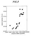
- Fig. 4 is a graph showing a relationship between an excessive oxygen and a volume resistivity.
- the excessive oxygen i.e., an amount of oxygen existing in aluminum nitride crystal grains
- the volume resistivity is extremely increased.
- a sintered body having a high volume resistivity not less than 1 x 10 12 ⁇ cm
- having a volume resistivity of not more than 1 x 10 10 ⁇ cm will co-exist. Its reason is assumable to be that even if oxygen forms solid-solution in aluminum nitride grains, the resistance is not decreased when the grain diameter is small.
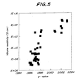
- Fig. 5 is a graph showing a relationship between a g-value obtained from an ESR spectrum and a volume resistivity. As is seen from this graph, when the g-value exceeds 2.000, the volume resistivity is extremely increased. On the other hand, when the g-value is not more than 2.000, a sintered body having a high volume resistivity (not less than 1 x 10 12 ⁇ cm) and that having a volume resistivity of not more than 1 x 10 10 ⁇ cm co-exist.
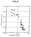
- Fig. 6 is a graph showing a relationship between a spin amount per unit mg of aluminum obtained from an ESR spectrum and a volume resistivity. As is seen from this result, when the spin amount was not less than 1 x 10 13 spins/mg, the volume resistivity was extremely decreased.
- the amounts of oxygen and metal impurities in the starting material were optimized, and the amount of yttrium was changed.
- the content of the yttrium in a sintered body is preferred to be not more than 1000 ppm, more preferably not less than 300 ppm.
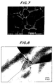
- Fig. 7 is a scanning electron photomicrograph showing a crystal structure of the sintered body No. 11.
- Fig. 8 is a transition electron photomicrograph showing an enlargement of the vicinity of a triple point of this sintered body.
- Fig. 9 is a transition electron photomicrograph showing an enlargement of a grain boundary of adjacent crystal grains. Though no intergranular phase is observed in the boundaries of adjacent crystal grains, an aluminum oxide phase has been formed at the triple point.
- Fig. 10 is a graph showing a result of an analysis by EDS (Energy Dispersive X-ray Spectrometer) of a grain boundary of adjacent crystal grains with respect to the sintered body No. 11 of an embodiment of the present invention, and it shows that the yttrium exists in a trace amount. However, the peak of "C" is attributed to the contamination of the sample.
- Fig. 11 is a graph showing a result of an analysis by EDS of the inside of a crystal grain with respect to the same sample. No peak of yttrium is observed and it shows existence of a peak of oxygen.
- Figs. 12 and 13 are graphs respectively showing results of analyses by EDS of the inside of a crystal grain with respect to the sintered body No. 16 in a comparative example. No peaks of oxygen and yttrium are observed.
- Fig. 14 is a graph showing a result of an analysis by EDS of a grain boundary in the interface of crystal grains with respect to the same sintered body as the above. A conspicuous peak of yttrium is observed. This intergranular phase containing a large amount of yttrium contributes to increase the resistance between adjacent crystal grains.
- Fig. 15 is a graph showing a result of an analysis by EDS of a triple point with respect to the sintered body No. 16 in a comparative example. A further conspicuous peak of yttrium is observed.
- Fig. 16 is a graph showing an X-ray diffraction peak with respect to the sintered body No. 11 in an embodiment of the present invention. As is seen from this graph, there is no peak corresponding to crystals of an yttrium compound. Therefore, yttrium does not constitute a crystalline phase at the boundary of crystal grains.
- Fig. 17 is a TEM photograph in a high magnification showing a crystal tissue near the grain boundary of adjacent crystal grains with respect to the sintered body No. 11 of an embodiment of the present invention.
- the crystal grains are present on the right and left hand sides, respectively, in this photograph, and an interface exists between crystal grains in the right and left directions.
- constituent atoms of a crystal lattice form a perfect orderly crystal lattice. It has been found that though the crystal lattice is slightly disordered in the vicinity of the grain boundary of the crystal grains, the width of the portion where the crystal lattice is disordered is extremely as narrow as about several numbers of atoms, that is, no more than 1 nm.
- Fig. 18 is a TEM photograph in a high magnification showing a crystal tissue near the grain boundary of adjacent crystal grains with respect to the sintered body No. 16 of a comparative example.
- a disorder of crystal lattice is recognized in the vicinity of the grain boundary between the right and left grains. Its width is about 1-3 nm. From the result of a restricted view field electron diffraction, crystalline precipitates were detected at the grain boundary. This disordering of the crystal lattice is assumed to be caused by fine precipitates deposited in grain boundaries.
- Figs. 19 and 20 are transition electron photomicrographs with respect to the sintered body No. 16 in a comparative example. At the triple points and grain boundaries, black precipitates (0.2 ⁇ m) were observed. As a result of observation of the precipitates by EDS, Y 2 Al 4 O 9 was detected. Besides, these precipitates were crystalline.
- the interface 6 between adjacent crystal grains 5A and 5B had an irregularly intermingled shape and was intricately bent.
- the width t of this intergranular phase was about 1-3 nm.
- the interface 2 between crystal grains 1A and 1B extended substantially straight, and the width was not more than 1 nm. Further, the deviation of the position of the grain boundary was on a level of several aluminum atoms.
- aluminum nitride sintered bodies of experimental run No. 51 - 63 shown in Tables 7 and 8 were produced.
- the starting powder aluminum nitride powder obtained by a reductive nitriding method was used. Amounts of oxygen and metal impurities in this starting powder are shown in Table 7 .
- Yttrium nitrate was dissolved in isopropyl alcohol to provide an additive solution. This additive solution was admixed with the aluminum nitride starting powder by using a pot mill. The amounts of the added yttrium as Y 2 O 3 are shown in Table 7.
- the total amount of metal impurities except yttrium was determined and shown in Table 7. Further, the content of yttrium (Y), a total oxygen content (O), a total carbon content (C), and excessive oxygen (the difference between the total oxygen content and the oxygen content in yttria) in the sintered bodies were shown in Table 7. Besides, the g-value, spin number, average particle diameter, thermal conductivity, strength, relative density and color were measured as aforementioned with respect to each sintered body. The results are shown in Table 8.
- the amount of yttria added to the starting powder was 5 % by weight, and in the sintered body it remained in an amount of about 3.7 % or 0.1 %, by weight.
- the oxygen content in the crystal particle was determined with an electron probe X-ray microanalyzer, and it was found to be 0.35 % or 0.21 %, by weight. Namely, since in experimental run No. 52 the hot press temperature was relatively higher, discharge of yttria proceeded on the sintering stage, and discharge of the oxygen from inside of the crystal particle also proceeded.
- the volume resistivity of the sintered body is in the order of 10 14 ⁇ cm in Comparative Example 51, and in the order of 10 12 ⁇ cm in Comparative Example 52.
- the volume resistivity is lower in Comparative Example 52. This is considered that grain growth proceeded with discharging yttria, more in Comparative Example 52.
- the amount of the oxygen in crystal grains determined by an electron probe X-ray microanalyzer is not less than 0.5 % by weight, and the amount of the "excessive oxygen” is also not less than 0.5 % by weight. Additionally, it has been found that most of the "excessive oxygen" is distributed within the crystal grains, except Examples 62 and 63.
- the yttria content in the sintered body is not more than 0.2 % by weight, the g-value is not more than 2.000, the spin amount is not less than 1.0 x 10 13 spins/mg, the average grain diameter is not less than 4 ⁇ m and the relative density is not less than 99 %.
- a volume resistivity of not more than 10 12 ⁇ cm has been obtained.
- the present inventors measured a spectrum by cathode luminescence with respect to each of the sintered bodies, experimental run numbers of which are shown in the aforementioned Tables 1-8. As the result, it has been found that an extreme decrease of the volume resistivity is recognized as mentioned above, in the sintered bodies that exhibit an intense main peak at 350-370 nm.
- the surface of the sintered body of Example 54 was mirror-polished with diamond paste, then the spectrum was observed according to the cathode luminescence method. The result is shown in Fig. 23.
- the axis of ordinate shows an intensity of luminescence and the axis of abscissa shows a wavelength of luminescence. A strong peak has appeared in the wavelength range of 350-370 nm, and a weak peak has appeared in the wavelength range of 650-750 nm.
- the surface of the sintered body of Comparative Example 52 was mirror-polished with diamond paste, then the spectrum was observed according to the cathode luminescence method. The result is shown in Fig. 24. As the result, weak peaks at about 340 nm, 500 nm and 600 nm are observed, respectively.
- Fig. 25 is shown comparison of Example 54 with Comparative Example 52 with respect to spectra obtained according to the cathode luminescence method.
- the luminescence intensity of the main peak in 350-370 nm that is characteristically shown in the sintered body according to the present invention is very high, as compared with each peak of the sintered body of Comparative Example.
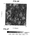
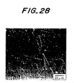
- Fig. 26 cathode luminescence two-dimensional mapping was conducted at a wavelength of 360 nm. The result is shown in Fig. 26. Besides, in Fig. 27 is shown a relationship between shades in the two-dimensional mapping shown in Fig. 26 and a luminescense intensity. Additionally, Fig. 28 is a scanning electron photomicrograph of a ceramic tissue with the same view field as Fig. 26.
- the shades in the two-dimensional mapping is considered to depend on the crystalline orientation of each crystal grain. Namely, in the case where a crystal grain has a crystalline orientation perpendicular to electron radiation, the luminescence intensity according to the cathode luminescence method is increased. Thus, the difference in crystalline orientation of each crystal grain shown in Fig. 28 may be a direct cause of variation of the shades shown in Fig. 26. Besides, in Fig. 26, a portion corresponding to the grain boundary is always dark and not luminous. From the above result of measurement, it has been found that a very strong luminescence at wavelength 360 nm is emitted from the inside of crystal grains.
- Metals can be embedded in the aluminum nitride sintered body according to the prevent invention.
- Articles embedded with an electrode can be used preferably particularly in an environment where impurities are abominated. Examples of such applications include: ceramic electrostatic chucks; ceramic heaters; and high frequency electrode apparatuses. The use for electrostatic chucks is particularly suitable.
- the metal embedded articles according to the invention are used as an electrostatic chuck, for example, for attracting semiconductor wafers, since a dielectric layer can be made to have a volume resistivity of not more than 1 x 10 12 ⁇ cm at room temperature, it may be possible to extremely improve attracting characteristics of the electrostatic chuck in the temperature range of around room temperature or below -60°C. In this case, even if the thickness of the dielectric layer is made to be not less than 500 ⁇ m, when voltage is applied, electric charge is transferred from the electrode onto the surface of the insulative dielectric layer, so that a sufficient attracting force can be obtained. Immediately after turning off the voltage, the electric charge is lost quickly. Therefore, the response for chucking or releasing wafer is also good. It has become possible thereby to attract and hold stably a large-sized semiconductor wafer of not less than 8 inches in the extremely wide temperature range from a low temperature region of particularly about -60°C to a high temperature region of not less than 300°C.
- Such a metal member to be embedded in the aluminum nitride sintered body is preferred to be a plate-type metal bulk material.
- the metal member when the metal embedded article is an electrostatic chuck, the metal member is a plate-type electrode made from the metal bulk material.
- the term "plate- type metal bulk material” should be understood to mean a monolitic plate-type material formed of metal, for example, as shown in Fig. 30, other than a spiral or zigzag shaped wire or plate.
- the metal member since it is fired together with aluminum nitride powder, is preferred to be formed of a high melting metal.
- a high melting metal include: tantalum; tungsten: molybdenum; platinum; rhenium; hafnium; and alloys thereof. From the viewpoint of preventing semiconductors from contamination, tantalum, tungsten, molybdenum, platinum and alloys thereof are more preferred.
- objects to be treated with electrostatic chucks include an aluminum wafer and the like, in addition to the semiconductor wafer.
- Examples of such a plate-type bulk material include the followings:
- the shape of the mesh and the wire diameter of such a metal net are not specifically limited. However, 150 meshes with wire of 0.03 mm diameter to 6 meshes with wire of 0.5 mm diameter could be employed without problems. Further, the cross sectional shape of the wire material constructing the metal net may be various rolled shapes such as circular, ellipse, rectangular and the like. Here, one mesh is meant by one wire per an inch.
- the electrodes of the electrostatic chuck can be connected with a high frequency power source to supply the electrodes with a high frequency voltage together with a DC voltage, whereby this electrode also can be used as an electrode for generating plasma.
- the thickness of the electrode is preferred to be not less than 430 ⁇ m.
- the electrode is formed of a metal bulk body.
- a dielectric layer having a thickness ranging 0.5 - 5.0 mm since a self-exotherm due to dielectric loss is not so high, can be used as a high frequency electrode with no problem.
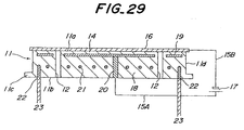
- Fig. 29 is a cross sectional view schematically showing an embodiment of the electrostatic chuck.
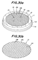
- Fig. 30a is a perspective view showing the electrostatic chuck shown in Fig. 29, with a part cut away.
- Fig. 30b is a perspective view showing an electrode 13 formed of a metal net.
- a ring shaped flange 11c is provided on a circumferential side surface 11d of a substantially disc shaped substrate 11.
- An electrode 19 formed of a metal net 13 is embedded in the substrate 11.
- a dielectric layer 14 having a predetermined thickness is formed on the surface 11a for loading a semiconductor wafer 16.
- a terminal 20 is embedded in a supporting portion 18 of the substrate. One end surface of the terminal 20 is exposed at the rear surface 11b of the substrate 11.
- Through-holes 12 for inserting a pin for elevating and lowering the semiconductor wafer 16 are formed at predetermined positions of the substrate 11 .
- a DC power source 17 is connected via an electric wire 5A to the terminal 20, and a negative electrode of the DC power source 17 is connected via an electric wire 5B to the semiconductor wafer 16.
- the electrode 19 is formed of a metal net 13 as shown in Figs. 30a and 30b.
- the metal net 13 comprises a circular rim wire 13a and wires 13b arranged crosswise within the rim wire 13a, thus forming meshes 24 in the net.
- a resistance heating element 21 is embedded between the electrode 19 and the back surface 11b. Both the end portions of the resistance heating element 21 are connected to the terminals 22, respectively, and the terminals 22 are connected to the external terminals 23, respectively.
- This resistance heating element is for heating the semiconductor wafer during chucking the wafer and not always necessary.
- the aluminum nitride sintered body according to the invention can be used as a substrate for semiconductor manufacturing apparatuses, such as susceptors for holding a semiconductor wafer, dummy wafers, shadow rings. tubes for generating a high frequency plasma, domes for generating a high frequency plasma, high frequency transmitting windows, lift pins for supporting a semiconductor wafer, shower plates and the like.
- a heating source for induced heating (a heating material) can be exemplified.
- the sintered body according to the invention since it has a high purity as well as a high corrosive resistance against plasma, can be utilized as a heating source for induced heating to be used in a plasma atmosphere.
- the present inventors manufactured an electrostatic chuck as shown in Fig. 29.
- a starting powder an aluminum nitride powder obtained by a reductive nitriding method was employed.
- the amount of the oxygen was 1.2 % by weight and the amount of the metal impurities was 90 ppm in the starting powder.
- An additive solution was prepared by dissolving yttrium nitrate in isopropyl alcohol, and this additive solution was admixed with the aluminum nitride starting powder by using a pot mill.
- the proportion of the mixed yttria as Y 2 O 3 was 0.05 % by weight.
- a metal net 13 made of molybdenum was used as the electrode 19.
- the metal net 13 was knitted with a molybdenum wire having a diameter of 0.5 mm, at a density of 15 ends per 1 inch.
- the metal net 13 was embedded in the aforementioned starting powder, a pressure of 100 kgf/cm 2 was applied in a perpendicular direction of to the metal net 13 and axial press molding was conducted to provide a disc-type shaped body having a diameter of 200 mm.
- This disc-type shaped body was received in a hot press mold and sealed hermetically.
- the temperature was increased at a temperature increasing rate of 300°C/hour. In this case, the pressure was reduced in the range of from room temperature to 1000°C. Concurrently with the temperature increase up above this temperature range, the pressure was raised.
- the maximum temperature set at 2000°C was held for 5 hours.
- the total amount of the metal impurities except yttrium was 90 ppm
- the yttrium (Y) was 320 ppm
- the total oxygen (O) was 0.90 % by weight
- the total carbon (C) was 0.03 % by weight
- an excessive oxygen (O) was 0.89 % by weight.
- this sintered body had a g-value of ESR spectrum of 1.9977, a peak ratio (Al/Mn) of 3.50, a spin number of 2.9 x 10 13 spins/mg, an average grain diameter of 11 ⁇ m, a thermal conductivity of 60, a strength of 320 MPa, and a relative density of 99.9 %.
- the spectrum was measured by means of a cathode luminescence method, and the same main peak as that of Fig. 23 was observed in the wavelength range of 350-370 nm.
- the mount of the oxygen in crystal grains determined by an electron probe X-ray microanalyzer was 0.79 % by weight.
- the surface of the dielectric layer of the obtained sintered body was machined, to make the thickness of the dielectric layer 14 to be 1 mm.
- Through-holes 12 were perforated from the back surface side 11b of the sintered body with a machining center. Further, a terminal 20 was connected to electrodes 19. However, the resistance heating element was not embedded.
- the electrostatic chuck had a dimension of 200 mm diameter and 12 mm thickness. The attracting force of this electrostatic chuck was determined. The attracting force that was measured at an interval of 100°C from room temperature to 300°C was 60-100g/cm 2 at any temperatures. Besides, the volume resistivity at room temperature of the dielectric layer was 1 x 10 7 ⁇ cm.
- a novel aluminum nitride sintered body with a high purity and a low volume resistivity can be provided.
- a novel electronic functional material comprising such an aluminum nitride sintered body, which has a volume resistivity on a semiconductor level, and an electrostatic chuck using such an aluminum nitride sintered body.
Applications Claiming Priority (5)
| Application Number | Priority Date | Filing Date | Title |
|---|---|---|---|
| JP9955796 | 1996-03-29 | ||
| JP9955796 | 1996-03-29 | ||
| JP07279997A JP3457495B2 (ja) | 1996-03-29 | 1997-03-11 | 窒化アルミニウム焼結体、金属埋設品、電子機能材料および静電チャック |
| JP7279997 | 1997-03-11 | ||
| EP97302083A EP0798278B1 (fr) | 1996-03-29 | 1997-03-26 | Corps fritté en nitrure d'aluminium, article intégré en métal, matériau d'un fonctionnement électronique et dispositif de serrage électrostatique |
Related Parent Applications (2)
| Application Number | Title | Priority Date | Filing Date |
|---|---|---|---|
| EP97302083A Division EP0798278B1 (fr) | 1996-03-29 | 1997-03-26 | Corps fritté en nitrure d'aluminium, article intégré en métal, matériau d'un fonctionnement électronique et dispositif de serrage électrostatique |
| EP97302083A Division-Into EP0798278B1 (fr) | 1996-03-29 | 1997-03-26 | Corps fritté en nitrure d'aluminium, article intégré en métal, matériau d'un fonctionnement électronique et dispositif de serrage électrostatique |
Publications (2)
| Publication Number | Publication Date |
|---|---|
| EP1128425A1 true EP1128425A1 (fr) | 2001-08-29 |
| EP1128425B1 EP1128425B1 (fr) | 2006-06-21 |
Family
ID=26413933
Family Applications (2)
| Application Number | Title | Priority Date | Filing Date |
|---|---|---|---|
| EP97302083A Expired - Lifetime EP0798278B1 (fr) | 1996-03-29 | 1997-03-26 | Corps fritté en nitrure d'aluminium, article intégré en métal, matériau d'un fonctionnement électronique et dispositif de serrage électrostatique |
| EP01103195A Expired - Lifetime EP1128425B1 (fr) | 1996-03-29 | 1997-03-26 | Corps fritté en nitrure d'aluminium, article ayant un metal encastré, materiau électronique fonctionnel et mandrin de serrage électrostatique |
Family Applications Before (1)
| Application Number | Title | Priority Date | Filing Date |
|---|---|---|---|
| EP97302083A Expired - Lifetime EP0798278B1 (fr) | 1996-03-29 | 1997-03-26 | Corps fritté en nitrure d'aluminium, article intégré en métal, matériau d'un fonctionnement électronique et dispositif de serrage électrostatique |
Country Status (6)
| Country | Link |
|---|---|
| US (1) | US6001760A (fr) |
| EP (2) | EP0798278B1 (fr) |
| JP (1) | JP3457495B2 (fr) |
| KR (1) | KR100268481B1 (fr) |
| DE (2) | DE69736205T2 (fr) |
| TW (1) | TW561138B (fr) |
Cited By (1)
| Publication number | Priority date | Publication date | Assignee | Title |
|---|---|---|---|---|
| EP1314707A2 (fr) * | 2001-11-26 | 2003-05-28 | Ngk Insulators, Ltd. | Céramiques à base de nitride d'aluminium, membres pour l'utilisation dans une système pour la production des semi-conducteurs, les membres ayant résistances contre la corrosion et les membres conductives |
Families Citing this family (85)
| Publication number | Priority date | Publication date | Assignee | Title |
|---|---|---|---|---|
| JP3670416B2 (ja) | 1995-11-01 | 2005-07-13 | 日本碍子株式会社 | 金属包含材および静電チャック |
| US5914613A (en) | 1996-08-08 | 1999-06-22 | Cascade Microtech, Inc. | Membrane probing system with local contact scrub |
| JP4236292B2 (ja) | 1997-03-06 | 2009-03-11 | 日本碍子株式会社 | ウエハー吸着装置およびその製造方法 |
| JPH10275524A (ja) * | 1997-03-31 | 1998-10-13 | Kyocera Corp | 耐プラズマ部材 |
| JP3670444B2 (ja) * | 1997-06-06 | 2005-07-13 | 日本碍子株式会社 | 窒化アルミニウム基複合体、電子機能材料、静電チャックおよび窒化アルミニウム基複合体の製造方法 |
| JP3318514B2 (ja) * | 1997-08-06 | 2002-08-26 | 日本碍子株式会社 | 半導体支持装置 |
| JP3433063B2 (ja) * | 1997-09-29 | 2003-08-04 | 日本碍子株式会社 | 窒化アルミニウム焼結体、電子機能材料および静電チャック |
| CA2252113A1 (fr) * | 1997-10-29 | 1999-04-29 | Yoshihiko Numata | Substrat et procede pour le produire |
| US5909355A (en) * | 1997-12-02 | 1999-06-01 | Applied Materials, Inc. | Ceramic electrostatic chuck and method of fabricating same |
| JPH11209182A (ja) * | 1998-01-22 | 1999-08-03 | Sumitomo Metal Ind Ltd | プラズマ耐食部材 |
| JPH11214491A (ja) * | 1998-01-22 | 1999-08-06 | Toshiba Ceramics Co Ltd | ウエハ保持装置及びその製造方法 |
| JP3527840B2 (ja) * | 1998-01-28 | 2004-05-17 | 京セラ株式会社 | 静電チャック |
| JP4013386B2 (ja) * | 1998-03-02 | 2007-11-28 | 住友電気工業株式会社 | 半導体製造用保持体およびその製造方法 |
| JP4003907B2 (ja) * | 1998-07-08 | 2007-11-07 | コバレントマテリアル株式会社 | 窒化アルミニウム焼結体からなる半導体製造装置関連製品及びその製造方法並びに静電チャック、サセプタ、ダミーウエハ、クランプリング及びパーティクルキャッチャー |
| US6256882B1 (en) | 1998-07-14 | 2001-07-10 | Cascade Microtech, Inc. | Membrane probing system |
| US6445202B1 (en) | 1999-06-30 | 2002-09-03 | Cascade Microtech, Inc. | Probe station thermal chuck with shielding for capacitive current |
| JP3273773B2 (ja) | 1999-08-12 | 2002-04-15 | イビデン株式会社 | 半導体製造・検査装置用セラミックヒータ、半導体製造・検査装置用静電チャックおよびウエハプローバ用チャックトップ |
| JP2001064079A (ja) * | 1999-08-25 | 2001-03-13 | Sumitomo Electric Ind Ltd | 窒化アルミニウム焼結体及びその製造方法 |
| US6900149B1 (en) | 1999-09-06 | 2005-05-31 | Ibiden Co., Ltd. | Carbon-containing aluminum nitride sintered compact and ceramic substrate for use in equipment for manufacturing or inspecting semiconductor |
| JP4447750B2 (ja) * | 1999-09-30 | 2010-04-07 | 日本碍子株式会社 | 窒化アルミニウム焼結体および半導体製造用部材 |
| US20040222211A1 (en) * | 1999-12-28 | 2004-11-11 | Ibiden Co., Ltd. | Carbon-containing aluminum nitride sintered body, and ceramic substrate for a semiconductor producing/examining device |
| JP3228924B2 (ja) | 2000-01-21 | 2001-11-12 | イビデン株式会社 | 半導体製造・検査装置用セラミックヒータ |
| US6888236B2 (en) * | 2000-03-07 | 2005-05-03 | Ibiden Co., Ltd. | Ceramic substrate for manufacture/inspection of semiconductor |
| JP2001278665A (ja) * | 2000-03-29 | 2001-10-10 | Kyocera Corp | セラミック抵抗体及び基板支持体 |
| TWI254403B (en) * | 2000-05-19 | 2006-05-01 | Ngk Insulators Ltd | Electrostatic clamper, and electrostatic attracting structures |
| JP2001342070A (ja) * | 2000-05-29 | 2001-12-11 | Kyocera Corp | セラミック抵抗体及び保持部材 |
| JP3605347B2 (ja) * | 2000-06-27 | 2004-12-22 | 京セラ株式会社 | 電極内蔵セラミックスの製造方法、吸着装置及び半導体製造装置 |
| WO2002009171A1 (fr) | 2000-07-25 | 2002-01-31 | Ibiden Co., Ltd. | Substrat ceramique pour appareil de fabrication/inspection de semi-conducteurs, element chauffant en ceramique, dispositif de retenue electrostatique sans attache et substrat pour testeur de tranches |
| JP2002047067A (ja) * | 2000-07-31 | 2002-02-12 | Kyocera Corp | 電極内蔵セラミックス及びその製造方法 |
| US6914423B2 (en) | 2000-09-05 | 2005-07-05 | Cascade Microtech, Inc. | Probe station |
| US6965226B2 (en) | 2000-09-05 | 2005-11-15 | Cascade Microtech, Inc. | Chuck for holding a device under test |
| US6607836B2 (en) | 2000-10-23 | 2003-08-19 | Ngk Insulators, Ltd. | Material of low volume resistivity, an aluminum nitride sintered body and a member used for the production of semiconductors |
| DE10143173A1 (de) | 2000-12-04 | 2002-06-06 | Cascade Microtech Inc | Wafersonde |
| TWI243158B (en) * | 2000-12-21 | 2005-11-11 | Ngk Insulators Ltd | Aluminum nitride sintered bodies |
| JP4514379B2 (ja) * | 2000-12-21 | 2010-07-28 | 日本碍子株式会社 | 窒化アルミニウム焼結体及び半導体製造装置用部材 |
| JP3740383B2 (ja) * | 2001-05-28 | 2006-02-01 | 京セラ株式会社 | 保持装置 |
| JP2003012376A (ja) * | 2001-06-27 | 2003-01-15 | Kyocera Corp | 抵抗体及びその製造方法並びに保持装置 |
| KR100698871B1 (ko) * | 2001-07-03 | 2007-03-22 | 삼성전자주식회사 | 건식 식각 장치 |
| JP2003040674A (ja) * | 2001-07-25 | 2003-02-13 | Kyocera Corp | 抵抗体及びその製造方法並びに保持装置 |
| JP4145097B2 (ja) * | 2001-08-20 | 2008-09-03 | 日本碍子株式会社 | 低誘電正接材料および炭化珪素焼結体の誘電正接を制御する方法 |
| WO2003052435A1 (fr) | 2001-08-21 | 2003-06-26 | Cascade Microtech, Inc. | Systeme de detection a membrane |
| JP4493264B2 (ja) * | 2001-11-26 | 2010-06-30 | 日本碍子株式会社 | 窒化アルミニウム質セラミックス、半導体製造用部材および耐蝕性部材 |
| JP4243943B2 (ja) | 2002-04-22 | 2009-03-25 | 日本碍子株式会社 | 窒化アルミニウム材料および半導体製造用部材 |
| JP3808407B2 (ja) * | 2002-07-05 | 2006-08-09 | 住友大阪セメント株式会社 | 電極内蔵型サセプタ及びその製造方法 |
| US6986865B2 (en) * | 2002-07-10 | 2006-01-17 | Watlow Electric Manufacturing Company | Method for manufacturing an electrostatic chuck |
| JP4386695B2 (ja) * | 2002-11-14 | 2009-12-16 | 日本碍子株式会社 | 窒化アルミニウム焼結体の製造方法 |
| US6982125B2 (en) * | 2002-12-23 | 2006-01-03 | Saint-Gobain Ceramics & Plastics, Inc. | ALN material and electrostatic chuck incorporating same |
| JP4424659B2 (ja) | 2003-02-28 | 2010-03-03 | 日本碍子株式会社 | 窒化アルミニウム質材料および半導体製造装置用部材 |
| US7492172B2 (en) | 2003-05-23 | 2009-02-17 | Cascade Microtech, Inc. | Chuck for holding a device under test |
| US7057404B2 (en) | 2003-05-23 | 2006-06-06 | Sharp Laboratories Of America, Inc. | Shielded probe for testing a device under test |
| JP4499431B2 (ja) | 2003-07-07 | 2010-07-07 | 日本碍子株式会社 | 窒化アルミニウム焼結体、静電チャック、導電性部材、半導体製造装置用部材及び窒化アルミニウム焼結体の製造方法 |
| US7250626B2 (en) | 2003-10-22 | 2007-07-31 | Cascade Microtech, Inc. | Probe testing structure |
| US7187188B2 (en) | 2003-12-24 | 2007-03-06 | Cascade Microtech, Inc. | Chuck with integrated wafer support |
| DE202004021093U1 (de) | 2003-12-24 | 2006-09-28 | Cascade Microtech, Inc., Beaverton | Aktiver Halbleiterscheibenmessfühler |
| WO2005092789A1 (fr) * | 2004-03-29 | 2005-10-06 | Denki Kagaku Kogyo Kabushiki Kaisha | Poudre de nitrure d’aluminium et pastille frittée de nitrure d’aluminium |
| US7369393B2 (en) * | 2004-04-15 | 2008-05-06 | Saint-Gobain Ceramics & Plastics, Inc. | Electrostatic chucks having barrier layer |
| DE202005021435U1 (de) | 2004-09-13 | 2008-02-28 | Cascade Microtech, Inc., Beaverton | Doppelseitige Prüfaufbauten |
| US7535247B2 (en) | 2005-01-31 | 2009-05-19 | Cascade Microtech, Inc. | Interface for testing semiconductors |
| US7656172B2 (en) | 2005-01-31 | 2010-02-02 | Cascade Microtech, Inc. | System for testing semiconductors |
| JP5062959B2 (ja) * | 2005-03-25 | 2012-10-31 | 日本碍子株式会社 | セラミックス部材及びその製造方法 |
| JP4987238B2 (ja) * | 2005-03-25 | 2012-07-25 | 日本碍子株式会社 | 窒化アルミニウム焼結体、半導体製造用部材及び窒化アルミニウム焼結体の製造方法 |
| KR100917778B1 (ko) * | 2005-04-22 | 2009-09-21 | 주식회사 코미코 | 치밀질 질화알루미늄 소결체, 그 제조 방법 및 상기소결체를 이용한 반도체 제조용 부재 |
| KR100918190B1 (ko) * | 2005-04-22 | 2009-09-22 | 주식회사 코미코 | 치밀질 질화알루미늄 소결체, 그 제조 방법 및 상기소결체를 이용한 반도체 제조용 부재 |
| JP2006045059A (ja) * | 2005-09-05 | 2006-02-16 | Ngk Insulators Ltd | 窒化アルミニウム質焼結体、耐蝕性部材、金属埋設品および半導体保持装置 |
| JP4753851B2 (ja) * | 2005-12-19 | 2011-08-24 | 日本碍子株式会社 | 窒化アルミニウム粉末、窒化アルミニウム質セラミックス焼結体、半導体製造装置用部材、窒化アルミニウム発光材料、及び窒化アルミニウム粉末の製造方法 |
| JP4740002B2 (ja) | 2006-03-20 | 2011-08-03 | 日本碍子株式会社 | 窒化アルミニウム焼結体、半導体製造装置用部材、及び窒化アルミニウム焼結体の製造方法 |
| US7764072B2 (en) | 2006-06-12 | 2010-07-27 | Cascade Microtech, Inc. | Differential signal probing system |
| US7403028B2 (en) | 2006-06-12 | 2008-07-22 | Cascade Microtech, Inc. | Test structure and probe for differential signals |
| US7723999B2 (en) | 2006-06-12 | 2010-05-25 | Cascade Microtech, Inc. | Calibration structures for differential signal probing |
| US7848075B2 (en) * | 2006-07-19 | 2010-12-07 | Ngk Insulators, Ltd. | Electrostatic chuck with heater |
| KR101256878B1 (ko) * | 2006-11-23 | 2013-05-02 | 주식회사 코미코 | 정전척용 질화 알루미늄 소결체 |
| JP5121268B2 (ja) | 2007-03-27 | 2013-01-16 | 日本碍子株式会社 | 窒化アルミニウム焼結体及び半導体製造装置用部材 |
| WO2009013984A1 (fr) * | 2007-07-24 | 2009-01-29 | Kabushiki Kaisha Toshiba | ÉLÉMENT AlN POUR UN APPAREIL DE DÉPÔT EN PHASE VAPEUR DE COMPOSÉ SEMI-CONDUCTEUR ET PROCÉDÉ DE FABRICATION DE COMPOSÉ SEMI-CONDUCTEUR UTILISANT CELUI-CI |
| US7876114B2 (en) | 2007-08-08 | 2011-01-25 | Cascade Microtech, Inc. | Differential waveguide probe |
| US7888957B2 (en) | 2008-10-06 | 2011-02-15 | Cascade Microtech, Inc. | Probing apparatus with impedance optimized interface |
| WO2010059247A2 (fr) | 2008-11-21 | 2010-05-27 | Cascade Microtech, Inc. | Coupon amovible pour appareil de sondage |
| US8319503B2 (en) | 2008-11-24 | 2012-11-27 | Cascade Microtech, Inc. | Test apparatus for measuring a characteristic of a device under test |
| WO2010109960A1 (fr) * | 2009-03-26 | 2010-09-30 | 株式会社東芝 | Substrat en nitrure d'aluminium, carte de circuit en nitrure d'aluminium, dispositif à semi-conducteur, et procede de fabrication de substrat en nitrure d'aluminium |
| WO2013111363A1 (fr) * | 2012-01-26 | 2013-08-01 | 京セラ株式会社 | Porte-substrat électrostatique |
| KR102430454B1 (ko) | 2014-08-15 | 2022-08-05 | 어플라이드 머티어리얼스, 인코포레이티드 | 플라즈마 강화 화학 기상 증착 시스템에서 높은 온도들로 압축 또는 인장 응력을 갖는 웨이퍼들을 프로세싱하는 방법 및 장치 |
| JP6338998B2 (ja) * | 2014-10-23 | 2018-06-06 | 国立大学法人九州工業大学 | 蛍光素子 |
| KR101757069B1 (ko) | 2015-11-26 | 2017-07-13 | 한국세라믹기술원 | 알루미나 복합체 세라믹스 조성물 및 그의 제조방법 |
| JP6875799B2 (ja) * | 2016-07-27 | 2021-05-26 | 日本特殊陶業株式会社 | 窒化アルミニウム焼結体 |
| KR102552189B1 (ko) | 2020-12-21 | 2023-07-05 | 한국세라믹기술원 | 질화 알루미늄 세라믹스 조성물 및 그의 제조방법 |
| CN116768633A (zh) * | 2023-06-20 | 2023-09-19 | 苏州艾成科技技术有限公司 | 一种半导体用AlN组成成分及其制造方法 |
Citations (3)
| Publication number | Priority date | Publication date | Assignee | Title |
|---|---|---|---|---|
| EP0147101A2 (fr) * | 1983-12-12 | 1985-07-03 | Kabushiki Kaisha Toshiba | Corps céramique fritté en nitrure d'aluminium à conductibilité thermique élevée |
| FR2637887A1 (en) * | 1983-05-13 | 1990-04-20 | Tokuyama Soda Kk | Fine aluminium nitride powder |
| US5376601A (en) * | 1991-05-30 | 1994-12-27 | Kyocera Corporation | Sintered product of aluminum nitride, a process for the preparation thereof, and a baking jig using the same |
Family Cites Families (16)
| Publication number | Priority date | Publication date | Assignee | Title |
|---|---|---|---|---|
| GB2087854B (en) * | 1980-10-09 | 1983-12-07 | Vasipari Kutato Intezet | Stamping powder and dies made thereof |
| HU185474B (en) * | 1981-11-10 | 1985-02-28 | Almasfuezitoei Timfoeldgyar | Process for preparing alpha-aluminium oxyde poor in alkali for ceramic purposes |
| DE3347862C2 (fr) * | 1982-09-17 | 1988-05-11 | Tokuyama Soda K.K., Tokuyama, Yamaguchi, Jp | |
| JPS6065768A (ja) * | 1983-09-19 | 1985-04-15 | 株式会社トクヤマ | 窒化アルミニウム組成物およびその製造方法 |
| JPS6071575A (ja) * | 1983-09-26 | 1985-04-23 | 株式会社トクヤマ | 窒化アルミニウム焼結体及びその製造方法 |
| US4672046A (en) * | 1984-10-15 | 1987-06-09 | Tdk Corporation | Sintered aluminum nitride body |
| JPS6346032A (ja) * | 1986-08-13 | 1988-02-26 | Nippon Telegr & Teleph Corp <Ntt> | 画像情報転送制御方式 |
| US4847221A (en) * | 1987-01-13 | 1989-07-11 | Kabushiki Kaisha Toshiba | AlN sintered body having high thermal conductivity and a method of fabricating the same |
| US4833108A (en) * | 1987-03-28 | 1989-05-23 | Narumi China Corporation | Sintered body of aluminum nitride |
| CA1318691C (fr) * | 1987-08-28 | 1993-06-01 | Akira Yamakawa | Corps en nitrure d'aluminium et procede de fabrication |
| JPH01203270A (ja) * | 1988-02-08 | 1989-08-16 | Sumitomo Electric Ind Ltd | 高熱伝導性窒化アルミニウム焼結体及びその製造法 |
| EP0339903B1 (fr) * | 1988-04-26 | 1993-10-06 | Toto Ltd. | Méthode pour préparer du céramique diélectrique pour les plateaux de montage électrostatiques |
| US5250478A (en) * | 1988-07-28 | 1993-10-05 | Kyocera Corporation | Aluminum nitride sintered body and process for preparation thereof |
| JP3447305B2 (ja) * | 1991-07-30 | 2003-09-16 | 京セラ株式会社 | 静電チャック |
| US5413360A (en) * | 1992-12-01 | 1995-05-09 | Kyocera Corporation | Electrostatic chuck |
| JP3670416B2 (ja) * | 1995-11-01 | 2005-07-13 | 日本碍子株式会社 | 金属包含材および静電チャック |
-
1997
- 1997-03-11 JP JP07279997A patent/JP3457495B2/ja not_active Expired - Lifetime
- 1997-03-25 TW TW086103801A patent/TW561138B/zh not_active IP Right Cessation
- 1997-03-25 US US08/824,560 patent/US6001760A/en not_active Expired - Lifetime
- 1997-03-26 DE DE69736205T patent/DE69736205T2/de not_active Expired - Lifetime
- 1997-03-26 EP EP97302083A patent/EP0798278B1/fr not_active Expired - Lifetime
- 1997-03-26 DE DE69706734T patent/DE69706734T2/de not_active Expired - Lifetime
- 1997-03-26 EP EP01103195A patent/EP1128425B1/fr not_active Expired - Lifetime
- 1997-03-29 KR KR1019970011434A patent/KR100268481B1/ko active IP Right Grant
Patent Citations (3)
| Publication number | Priority date | Publication date | Assignee | Title |
|---|---|---|---|---|
| FR2637887A1 (en) * | 1983-05-13 | 1990-04-20 | Tokuyama Soda Kk | Fine aluminium nitride powder |
| EP0147101A2 (fr) * | 1983-12-12 | 1985-07-03 | Kabushiki Kaisha Toshiba | Corps céramique fritté en nitrure d'aluminium à conductibilité thermique élevée |
| US5376601A (en) * | 1991-05-30 | 1994-12-27 | Kyocera Corporation | Sintered product of aluminum nitride, a process for the preparation thereof, and a baking jig using the same |
Cited By (3)
| Publication number | Priority date | Publication date | Assignee | Title |
|---|---|---|---|---|
| EP1314707A2 (fr) * | 2001-11-26 | 2003-05-28 | Ngk Insulators, Ltd. | Céramiques à base de nitride d'aluminium, membres pour l'utilisation dans une système pour la production des semi-conducteurs, les membres ayant résistances contre la corrosion et les membres conductives |
| EP1314707A3 (fr) * | 2001-11-26 | 2003-10-01 | Ngk Insulators, Ltd. | Céramiques à base de nitride d'aluminium, membres pour l'utilisation dans une système pour la production des semi-conducteurs, les membres ayant résistances contre la corrosion et les membres conductives |
| US6884742B2 (en) | 2001-11-26 | 2005-04-26 | Ngk Insulators, Ltd. | Aluminum nitride ceramics, members for use in a system for producing semiconductors, corrosion resistant members and conductive members |
Also Published As
| Publication number | Publication date |
|---|---|
| DE69736205T2 (de) | 2007-05-16 |
| EP0798278A2 (fr) | 1997-10-01 |
| EP1128425B1 (fr) | 2006-06-21 |
| US6001760A (en) | 1999-12-14 |
| TW561138B (en) | 2003-11-11 |
| JPH09315867A (ja) | 1997-12-09 |
| DE69736205D1 (de) | 2006-08-03 |
| EP0798278B1 (fr) | 2001-09-19 |
| KR100268481B1 (ko) | 2000-10-16 |
| JP3457495B2 (ja) | 2003-10-20 |
| DE69706734D1 (de) | 2001-10-25 |
| EP0798278A3 (fr) | 1998-03-04 |
| DE69706734T2 (de) | 2002-07-04 |
| KR19980023985A (ko) | 1998-07-06 |
Similar Documents
| Publication | Publication Date | Title |
|---|---|---|
| EP0798278B1 (fr) | Corps fritté en nitrure d'aluminium, article intégré en métal, matériau d'un fonctionnement électronique et dispositif de serrage électrostatique | |
| US5998320A (en) | Aluminum nitride sintered body, metal including member, electrostatic chuck, method of producing aluminum nitride sintered body, and method of producing metal including member | |
| KR100617342B1 (ko) | 질화알루미늄 소결체, 정전 척, 도전성 부재, 반도체 제조장치용 부재 및 질화알루미늄 소결체의 제조 방법 | |
| KR101689054B1 (ko) | 알루미나 소결체, 이것을 구비하는 부재 및 반도체 제조장치 | |
| EP1088801B1 (fr) | Corps frittés en nitrure d'aluminium et pièces de fabrication des semiconducteurs les contenant | |
| EP0905106B1 (fr) | Corps fritté en nitrure d'aluminium, matériau ayant une fonction électronique et dispositif de serrage électrostatique | |
| EP1582509B1 (fr) | Corps dense fritté à base de cordiérite | |
| EP0896362B1 (fr) | Dispositif de support pour semi-conducteur | |
| US6641939B1 (en) | Transition metal oxide doped alumina and methods of making and using | |
| KR100706064B1 (ko) | 세라믹스 부재 및 그 제조 방법 | |
| KR101644000B1 (ko) | 정전 척 | |
| EP1881519B1 (fr) | Chauffage pour mandrin électrostatique | |
| EP3061739B1 (fr) | Siliziumnitrid-substrat und siliziumnitrid-leiterplatte mit diesem substrat | |
| EP0882689B1 (fr) | Corps composite à base de nitrure d'aluminium, materiau électronique foncitionnel, monture électrostatique et procédé de fabrication d'un corps composite à base d nitrure d'aluminium | |
| JP4571728B2 (ja) | 窒化珪素焼結体及びその製造方法 | |
| EP2189431B1 (fr) | Produit fritté de nitrure d'aluminium, procédé de sa production et mandrin électrostatique contenant ce produit | |
| US20020110709A1 (en) | Material of low volume resistivity, an aluminum nitride sintered body and a member used for the production of semiconductors | |
| EP1357097B1 (fr) | Matériau de nitrure d'aluminium et éléments utilisés pour la production de semi-conducteurs | |
| KR20230096465A (ko) | 세라믹 서셉터의 제조 방법 |
Legal Events
| Date | Code | Title | Description |
|---|---|---|---|
| PUAI | Public reference made under article 153(3) epc to a published international application that has entered the european phase |
Free format text: ORIGINAL CODE: 0009012 |
|
| AC | Divisional application: reference to earlier application |
Ref document number: 798278 Country of ref document: EP |
|
| AK | Designated contracting states |
Kind code of ref document: A1 Designated state(s): DE FR GB |
|
| 17P | Request for examination filed |
Effective date: 20011004 |
|
| RIN1 | Information on inventor provided before grant (corrected) |
Inventor name: TAKAHASHI, MICHIO Inventor name: MORI, YUKIMASA Inventor name: KATSUDA, YUJI, C/O NGK Inventor name: BESSHO, YUKI |
|
| AKX | Designation fees paid |
Free format text: DE FR GB |
|
| 17Q | First examination report despatched |
Effective date: 20040113 |
|
| GRAP | Despatch of communication of intention to grant a patent |
Free format text: ORIGINAL CODE: EPIDOSNIGR1 |
|
| RIN1 | Information on inventor provided before grant (corrected) |
Inventor name: TAKAHASHI, MICHIO Inventor name: BESSHO, YUKI Inventor name: MORI, YUKIMASA Inventor name: KATSUDA, YUJI |
|
| GRAS | Grant fee paid |
Free format text: ORIGINAL CODE: EPIDOSNIGR3 |
|
| GRAA | (expected) grant |
Free format text: ORIGINAL CODE: 0009210 |
|
| AC | Divisional application: reference to earlier application |
Ref document number: 0798278 Country of ref document: EP Kind code of ref document: P |
|
| AK | Designated contracting states |
Kind code of ref document: B1 Designated state(s): DE FR GB |
|
| REG | Reference to a national code |
Ref country code: GB Ref legal event code: FG4D |
|
| REF | Corresponds to: |
Ref document number: 69736205 Country of ref document: DE Date of ref document: 20060803 Kind code of ref document: P |
|
| ET | Fr: translation filed | ||
| PLBE | No opposition filed within time limit |
Free format text: ORIGINAL CODE: 0009261 |
|
| STAA | Information on the status of an ep patent application or granted ep patent |
Free format text: STATUS: NO OPPOSITION FILED WITHIN TIME LIMIT |
|
| 26N | No opposition filed |
Effective date: 20070322 |
|
| REG | Reference to a national code |
Ref country code: FR Ref legal event code: PLFP Year of fee payment: 20 |
|
| PGFP | Annual fee paid to national office [announced via postgrant information from national office to epo] |
Ref country code: DE Payment date: 20160322 Year of fee payment: 20 |
|
| PGFP | Annual fee paid to national office [announced via postgrant information from national office to epo] |
Ref country code: FR Payment date: 20160208 Year of fee payment: 20 Ref country code: GB Payment date: 20160323 Year of fee payment: 20 |
|
| REG | Reference to a national code |
Ref country code: DE Ref legal event code: R071 Ref document number: 69736205 Country of ref document: DE |
|
| REG | Reference to a national code |
Ref country code: GB Ref legal event code: PE20 Expiry date: 20170325 |
|
| PG25 | Lapsed in a contracting state [announced via postgrant information from national office to epo] |
Ref country code: GB Free format text: LAPSE BECAUSE OF EXPIRATION OF PROTECTION Effective date: 20170325 |