EP1029109B1 - Long life high temperature process chamber - Google Patents
Long life high temperature process chamber Download PDFInfo
- Publication number
- EP1029109B1 EP1029109B1 EP98957469A EP98957469A EP1029109B1 EP 1029109 B1 EP1029109 B1 EP 1029109B1 EP 98957469 A EP98957469 A EP 98957469A EP 98957469 A EP98957469 A EP 98957469A EP 1029109 B1 EP1029109 B1 EP 1029109B1
- Authority
- EP
- European Patent Office
- Prior art keywords
- chamber
- susceptor
- ring
- quartz
- silicon carbide
- Prior art date
- Legal status (The legal status is an assumption and is not a legal conclusion. Google has not performed a legal analysis and makes no representation as to the accuracy of the status listed.)
- Expired - Lifetime
Links
- 238000000034 method Methods 0.000 title claims description 16
- 230000008569 process Effects 0.000 title claims description 12
- VYPSYNLAJGMNEJ-UHFFFAOYSA-N silicon dioxide Inorganic materials O=[Si]=O VYPSYNLAJGMNEJ-UHFFFAOYSA-N 0.000 claims description 56
- 239000010453 quartz Substances 0.000 claims description 54
- HBMJWWWQQXIZIP-UHFFFAOYSA-N silicon carbide Chemical compound [Si+]#[C-] HBMJWWWQQXIZIP-UHFFFAOYSA-N 0.000 claims description 51
- 229910010271 silicon carbide Inorganic materials 0.000 claims description 49
- 239000007789 gas Substances 0.000 claims description 34
- 235000012431 wafers Nutrition 0.000 claims description 33
- 238000000151 deposition Methods 0.000 claims description 18
- 238000005229 chemical vapour deposition Methods 0.000 claims description 16
- 230000008021 deposition Effects 0.000 claims description 16
- 239000000376 reactant Substances 0.000 claims description 12
- 238000012545 processing Methods 0.000 claims description 10
- 239000007787 solid Substances 0.000 claims description 8
- 238000000576 coating method Methods 0.000 claims description 7
- 238000010438 heat treatment Methods 0.000 claims description 7
- 239000011248 coating agent Substances 0.000 claims description 5
- 238000010926 purge Methods 0.000 claims description 5
- 239000004065 semiconductor Substances 0.000 claims description 5
- 238000011144 upstream manufacturing Methods 0.000 claims description 4
- 239000000758 substrate Substances 0.000 claims description 3
- HMDDXIMCDZRSNE-UHFFFAOYSA-N [C].[Si] Chemical compound [C].[Si] HMDDXIMCDZRSNE-UHFFFAOYSA-N 0.000 claims description 2
- 239000012495 reaction gas Substances 0.000 claims description 2
- 230000000903 blocking effect Effects 0.000 claims 1
- 235000012239 silicon dioxide Nutrition 0.000 description 52
- 239000000463 material Substances 0.000 description 23
- 241000239290 Araneae Species 0.000 description 9
- OKTJSMMVPCPJKN-UHFFFAOYSA-N Carbon Chemical compound [C] OKTJSMMVPCPJKN-UHFFFAOYSA-N 0.000 description 9
- 229910002804 graphite Inorganic materials 0.000 description 9
- 239000010439 graphite Substances 0.000 description 9
- 238000004140 cleaning Methods 0.000 description 8
- 239000006096 absorbing agent Substances 0.000 description 6
- 150000001875 compounds Chemical class 0.000 description 3
- 238000001816 cooling Methods 0.000 description 3
- 238000004031 devitrification Methods 0.000 description 3
- 230000000694 effects Effects 0.000 description 3
- 238000012423 maintenance Methods 0.000 description 3
- 239000002245 particle Substances 0.000 description 3
- 229910052710 silicon Inorganic materials 0.000 description 3
- 229910052582 BN Inorganic materials 0.000 description 2
- PZNSFCLAULLKQX-UHFFFAOYSA-N Boron nitride Chemical compound N#B PZNSFCLAULLKQX-UHFFFAOYSA-N 0.000 description 2
- 239000011358 absorbing material Substances 0.000 description 2
- 230000008901 benefit Effects 0.000 description 2
- 239000000919 ceramic Substances 0.000 description 2
- 239000012459 cleaning agent Substances 0.000 description 2
- 238000009833 condensation Methods 0.000 description 2
- 230000005494 condensation Effects 0.000 description 2
- 230000006866 deterioration Effects 0.000 description 2
- 239000002019 doping agent Substances 0.000 description 2
- 238000004519 manufacturing process Methods 0.000 description 2
- 230000005855 radiation Effects 0.000 description 2
- 239000010703 silicon Substances 0.000 description 2
- 239000000126 substance Substances 0.000 description 2
- 229910052581 Si3N4 Inorganic materials 0.000 description 1
- 229910008310 Si—Ge Inorganic materials 0.000 description 1
- 230000003466 anti-cipated effect Effects 0.000 description 1
- 238000013459 approach Methods 0.000 description 1
- 238000006243 chemical reaction Methods 0.000 description 1
- 238000010276 construction Methods 0.000 description 1
- 239000002826 coolant Substances 0.000 description 1
- PMHQVHHXPFUNSP-UHFFFAOYSA-M copper(1+);methylsulfanylmethane;bromide Chemical compound Br[Cu].CSC PMHQVHHXPFUNSP-UHFFFAOYSA-M 0.000 description 1
- 230000008878 coupling Effects 0.000 description 1
- 238000010168 coupling process Methods 0.000 description 1
- 238000005859 coupling reaction Methods 0.000 description 1
- 230000001351 cycling effect Effects 0.000 description 1
- 238000005137 deposition process Methods 0.000 description 1
- 238000000407 epitaxy Methods 0.000 description 1
- 238000005530 etching Methods 0.000 description 1
- 229910052736 halogen Inorganic materials 0.000 description 1
- 150000002367 halogens Chemical class 0.000 description 1
- 230000007246 mechanism Effects 0.000 description 1
- 238000005457 optimization Methods 0.000 description 1
- TWNQGVIAIRXVLR-UHFFFAOYSA-N oxo(oxoalumanyloxy)alumane Chemical compound O=[Al]O[Al]=O TWNQGVIAIRXVLR-UHFFFAOYSA-N 0.000 description 1
- 230000002093 peripheral effect Effects 0.000 description 1
- 230000002028 premature Effects 0.000 description 1
- 230000003449 preventive effect Effects 0.000 description 1
- 238000012797 qualification Methods 0.000 description 1
- 230000000284 resting effect Effects 0.000 description 1
- 230000035939 shock Effects 0.000 description 1
- 239000000377 silicon dioxide Substances 0.000 description 1
- HQVNEWCFYHHQES-UHFFFAOYSA-N silicon nitride Chemical compound N12[Si]34N5[Si]62N3[Si]51N64 HQVNEWCFYHHQES-UHFFFAOYSA-N 0.000 description 1
- 238000001228 spectrum Methods 0.000 description 1
- 239000002470 thermal conductor Substances 0.000 description 1
- 238000005382 thermal cycling Methods 0.000 description 1
Images


Classifications
-
- C—CHEMISTRY; METALLURGY
- C23—COATING METALLIC MATERIAL; COATING MATERIAL WITH METALLIC MATERIAL; CHEMICAL SURFACE TREATMENT; DIFFUSION TREATMENT OF METALLIC MATERIAL; COATING BY VACUUM EVAPORATION, BY SPUTTERING, BY ION IMPLANTATION OR BY CHEMICAL VAPOUR DEPOSITION, IN GENERAL; INHIBITING CORROSION OF METALLIC MATERIAL OR INCRUSTATION IN GENERAL
- C23C—COATING METALLIC MATERIAL; COATING MATERIAL WITH METALLIC MATERIAL; SURFACE TREATMENT OF METALLIC MATERIAL BY DIFFUSION INTO THE SURFACE, BY CHEMICAL CONVERSION OR SUBSTITUTION; COATING BY VACUUM EVAPORATION, BY SPUTTERING, BY ION IMPLANTATION OR BY CHEMICAL VAPOUR DEPOSITION, IN GENERAL
- C23C16/00—Chemical coating by decomposition of gaseous compounds, without leaving reaction products of surface material in the coating, i.e. chemical vapour deposition [CVD] processes
- C23C16/44—Chemical coating by decomposition of gaseous compounds, without leaving reaction products of surface material in the coating, i.e. chemical vapour deposition [CVD] processes characterised by the method of coating
- C23C16/455—Chemical coating by decomposition of gaseous compounds, without leaving reaction products of surface material in the coating, i.e. chemical vapour deposition [CVD] processes characterised by the method of coating characterised by the method used for introducing gases into reaction chamber or for modifying gas flows in reaction chamber
- C23C16/45587—Mechanical means for changing the gas flow
- C23C16/45591—Fixed means, e.g. wings, baffles
-
- H—ELECTRICITY
- H01—ELECTRIC ELEMENTS
- H01L—SEMICONDUCTOR DEVICES NOT COVERED BY CLASS H10
- H01L21/00—Processes or apparatus adapted for the manufacture or treatment of semiconductor or solid state devices or of parts thereof
- H01L21/67—Apparatus specially adapted for handling semiconductor or electric solid state devices during manufacture or treatment thereof; Apparatus specially adapted for handling wafers during manufacture or treatment of semiconductor or electric solid state devices or components ; Apparatus not specifically provided for elsewhere
- H01L21/67005—Apparatus not specifically provided for elsewhere
- H01L21/67011—Apparatus for manufacture or treatment
- H01L21/67098—Apparatus for thermal treatment
- H01L21/67115—Apparatus for thermal treatment mainly by radiation
-
- C—CHEMISTRY; METALLURGY
- C23—COATING METALLIC MATERIAL; COATING MATERIAL WITH METALLIC MATERIAL; CHEMICAL SURFACE TREATMENT; DIFFUSION TREATMENT OF METALLIC MATERIAL; COATING BY VACUUM EVAPORATION, BY SPUTTERING, BY ION IMPLANTATION OR BY CHEMICAL VAPOUR DEPOSITION, IN GENERAL; INHIBITING CORROSION OF METALLIC MATERIAL OR INCRUSTATION IN GENERAL
- C23C—COATING METALLIC MATERIAL; COATING MATERIAL WITH METALLIC MATERIAL; SURFACE TREATMENT OF METALLIC MATERIAL BY DIFFUSION INTO THE SURFACE, BY CHEMICAL CONVERSION OR SUBSTITUTION; COATING BY VACUUM EVAPORATION, BY SPUTTERING, BY ION IMPLANTATION OR BY CHEMICAL VAPOUR DEPOSITION, IN GENERAL
- C23C16/00—Chemical coating by decomposition of gaseous compounds, without leaving reaction products of surface material in the coating, i.e. chemical vapour deposition [CVD] processes
- C23C16/44—Chemical coating by decomposition of gaseous compounds, without leaving reaction products of surface material in the coating, i.e. chemical vapour deposition [CVD] processes characterised by the method of coating
- C23C16/4401—Means for minimising impurities, e.g. dust, moisture or residual gas, in the reaction chamber
-
- C—CHEMISTRY; METALLURGY
- C23—COATING METALLIC MATERIAL; COATING MATERIAL WITH METALLIC MATERIAL; CHEMICAL SURFACE TREATMENT; DIFFUSION TREATMENT OF METALLIC MATERIAL; COATING BY VACUUM EVAPORATION, BY SPUTTERING, BY ION IMPLANTATION OR BY CHEMICAL VAPOUR DEPOSITION, IN GENERAL; INHIBITING CORROSION OF METALLIC MATERIAL OR INCRUSTATION IN GENERAL
- C23C—COATING METALLIC MATERIAL; COATING MATERIAL WITH METALLIC MATERIAL; SURFACE TREATMENT OF METALLIC MATERIAL BY DIFFUSION INTO THE SURFACE, BY CHEMICAL CONVERSION OR SUBSTITUTION; COATING BY VACUUM EVAPORATION, BY SPUTTERING, BY ION IMPLANTATION OR BY CHEMICAL VAPOUR DEPOSITION, IN GENERAL
- C23C16/00—Chemical coating by decomposition of gaseous compounds, without leaving reaction products of surface material in the coating, i.e. chemical vapour deposition [CVD] processes
- C23C16/44—Chemical coating by decomposition of gaseous compounds, without leaving reaction products of surface material in the coating, i.e. chemical vapour deposition [CVD] processes characterised by the method of coating
- C23C16/458—Chemical coating by decomposition of gaseous compounds, without leaving reaction products of surface material in the coating, i.e. chemical vapour deposition [CVD] processes characterised by the method of coating characterised by the method used for supporting substrates in the reaction chamber
- C23C16/4582—Rigid and flat substrates, e.g. plates or discs
- C23C16/4583—Rigid and flat substrates, e.g. plates or discs the substrate being supported substantially horizontally
- C23C16/4585—Devices at or outside the perimeter of the substrate support, e.g. clamping rings, shrouds
-
- C—CHEMISTRY; METALLURGY
- C23—COATING METALLIC MATERIAL; COATING MATERIAL WITH METALLIC MATERIAL; CHEMICAL SURFACE TREATMENT; DIFFUSION TREATMENT OF METALLIC MATERIAL; COATING BY VACUUM EVAPORATION, BY SPUTTERING, BY ION IMPLANTATION OR BY CHEMICAL VAPOUR DEPOSITION, IN GENERAL; INHIBITING CORROSION OF METALLIC MATERIAL OR INCRUSTATION IN GENERAL
- C23C—COATING METALLIC MATERIAL; COATING MATERIAL WITH METALLIC MATERIAL; SURFACE TREATMENT OF METALLIC MATERIAL BY DIFFUSION INTO THE SURFACE, BY CHEMICAL CONVERSION OR SUBSTITUTION; COATING BY VACUUM EVAPORATION, BY SPUTTERING, BY ION IMPLANTATION OR BY CHEMICAL VAPOUR DEPOSITION, IN GENERAL
- C23C16/00—Chemical coating by decomposition of gaseous compounds, without leaving reaction products of surface material in the coating, i.e. chemical vapour deposition [CVD] processes
- C23C16/44—Chemical coating by decomposition of gaseous compounds, without leaving reaction products of surface material in the coating, i.e. chemical vapour deposition [CVD] processes characterised by the method of coating
- C23C16/48—Chemical coating by decomposition of gaseous compounds, without leaving reaction products of surface material in the coating, i.e. chemical vapour deposition [CVD] processes characterised by the method of coating by irradiation, e.g. photolysis, radiolysis, particle radiation
- C23C16/481—Chemical coating by decomposition of gaseous compounds, without leaving reaction products of surface material in the coating, i.e. chemical vapour deposition [CVD] processes characterised by the method of coating by irradiation, e.g. photolysis, radiolysis, particle radiation by radiant heating of the substrate
-
- C—CHEMISTRY; METALLURGY
- C23—COATING METALLIC MATERIAL; COATING MATERIAL WITH METALLIC MATERIAL; CHEMICAL SURFACE TREATMENT; DIFFUSION TREATMENT OF METALLIC MATERIAL; COATING BY VACUUM EVAPORATION, BY SPUTTERING, BY ION IMPLANTATION OR BY CHEMICAL VAPOUR DEPOSITION, IN GENERAL; INHIBITING CORROSION OF METALLIC MATERIAL OR INCRUSTATION IN GENERAL
- C23C—COATING METALLIC MATERIAL; COATING MATERIAL WITH METALLIC MATERIAL; SURFACE TREATMENT OF METALLIC MATERIAL BY DIFFUSION INTO THE SURFACE, BY CHEMICAL CONVERSION OR SUBSTITUTION; COATING BY VACUUM EVAPORATION, BY SPUTTERING, BY ION IMPLANTATION OR BY CHEMICAL VAPOUR DEPOSITION, IN GENERAL
- C23C16/00—Chemical coating by decomposition of gaseous compounds, without leaving reaction products of surface material in the coating, i.e. chemical vapour deposition [CVD] processes
- C23C16/44—Chemical coating by decomposition of gaseous compounds, without leaving reaction products of surface material in the coating, i.e. chemical vapour deposition [CVD] processes characterised by the method of coating
- C23C16/48—Chemical coating by decomposition of gaseous compounds, without leaving reaction products of surface material in the coating, i.e. chemical vapour deposition [CVD] processes characterised by the method of coating by irradiation, e.g. photolysis, radiolysis, particle radiation
- C23C16/482—Chemical coating by decomposition of gaseous compounds, without leaving reaction products of surface material in the coating, i.e. chemical vapour deposition [CVD] processes characterised by the method of coating by irradiation, e.g. photolysis, radiolysis, particle radiation using incoherent light, UV to IR, e.g. lamps
-
- G—PHYSICS
- G01—MEASURING; TESTING
- G01K—MEASURING TEMPERATURE; MEASURING QUANTITY OF HEAT; THERMALLY-SENSITIVE ELEMENTS NOT OTHERWISE PROVIDED FOR
- G01K1/00—Details of thermometers not specially adapted for particular types of thermometer
- G01K1/08—Protective devices, e.g. casings
- G01K1/12—Protective devices, e.g. casings for preventing damage due to heat overloading
-
- G—PHYSICS
- G01—MEASURING; TESTING
- G01K—MEASURING TEMPERATURE; MEASURING QUANTITY OF HEAT; THERMALLY-SENSITIVE ELEMENTS NOT OTHERWISE PROVIDED FOR
- G01K7/00—Measuring temperature based on the use of electric or magnetic elements directly sensitive to heat ; Power supply therefor, e.g. using thermoelectric elements
- G01K7/02—Measuring temperature based on the use of electric or magnetic elements directly sensitive to heat ; Power supply therefor, e.g. using thermoelectric elements using thermoelectric elements, e.g. thermocouples
- G01K7/04—Measuring temperature based on the use of electric or magnetic elements directly sensitive to heat ; Power supply therefor, e.g. using thermoelectric elements using thermoelectric elements, e.g. thermocouples the object to be measured not forming one of the thermoelectric materials
-
- H—ELECTRICITY
- H01—ELECTRIC ELEMENTS
- H01L—SEMICONDUCTOR DEVICES NOT COVERED BY CLASS H10
- H01L21/00—Processes or apparatus adapted for the manufacture or treatment of semiconductor or solid state devices or of parts thereof
- H01L21/67—Apparatus specially adapted for handling semiconductor or electric solid state devices during manufacture or treatment thereof; Apparatus specially adapted for handling wafers during manufacture or treatment of semiconductor or electric solid state devices or components ; Apparatus not specifically provided for elsewhere
- H01L21/683—Apparatus specially adapted for handling semiconductor or electric solid state devices during manufacture or treatment thereof; Apparatus specially adapted for handling wafers during manufacture or treatment of semiconductor or electric solid state devices or components ; Apparatus not specifically provided for elsewhere for supporting or gripping
- H01L21/687—Apparatus specially adapted for handling semiconductor or electric solid state devices during manufacture or treatment thereof; Apparatus specially adapted for handling wafers during manufacture or treatment of semiconductor or electric solid state devices or components ; Apparatus not specifically provided for elsewhere for supporting or gripping using mechanical means, e.g. chucks, clamps or pinches
- H01L21/68714—Apparatus specially adapted for handling semiconductor or electric solid state devices during manufacture or treatment thereof; Apparatus specially adapted for handling wafers during manufacture or treatment of semiconductor or electric solid state devices or components ; Apparatus not specifically provided for elsewhere for supporting or gripping using mechanical means, e.g. chucks, clamps or pinches the wafers being placed on a susceptor, stage or support
- H01L21/68785—Apparatus specially adapted for handling semiconductor or electric solid state devices during manufacture or treatment thereof; Apparatus specially adapted for handling wafers during manufacture or treatment of semiconductor or electric solid state devices or components ; Apparatus not specifically provided for elsewhere for supporting or gripping using mechanical means, e.g. chucks, clamps or pinches the wafers being placed on a susceptor, stage or support characterised by the mechanical construction of the susceptor, stage or support
Definitions
- This invention relates to apparatus for the high temperature processing of substrates and, more particularly to chemical vapor deposition (CVD) of materials on semiconductor wafers in a CVD reactor.
- CVD chemical vapor deposition
- the material being deposited not only deposits on the wafer, as is desired, but some material, not necessarily the same as that on the wafer, is also deposited on the reactor chamber walls and other parts within the reactor, notably the wafer support and a ring positioned around the wafer support in many reactors.
- the chamber Periodically, in order to maintain a repeatable process, the chamber has to be cleaned. Such chamber cleaning typically occurs by heating the wafer support, chamber walls and other parts to a suitably high temperature and admitting a flow of a halogen containing gas, for example HCl.
- Reactors for epitaxial deposition commonly employ a susceptor and a surrounding ring which helps to control the temperature of the susceptor. These components are usually made from graphite and coated with silicon carbide (SiC). Eventually, the HCl etch will penetrate the SiC coating which will cause rapid deterioration of the properties of the deposited films. Hence, they must be replaced.
- One type of well-known reactor employs thermocouples adjacent the ring for sensing the temperature of the rings surrounding the susceptor, which in turn is an indirect measure of the temperature of the susceptor and a wafer positioned on it. These thermocouples are usually sheathed with quartz. Frequent thermal cycling of the quartz to temperatures in excess of 1000°C causes devitrification of the quartz sheath and failure of the thermocouples, thus requiring replacement.
- the chamber is formed of quartz.
- a problem in high temperature chemical vapor deposition operations is that reactant gases may coat the interior of quartz chamber walls. Coatings on the chamber walls can have a number of undesirable aspects including the flaking of particles off the walls and the need for more frequent cleaning of the chamber. Some of the material depositing on the quartz chamber walls may not be etched away when the chamber is cleaned. If sufficient deposits gather, the quartz chamber locally loses its transparency and will heat rapidly by radiation from the lamps conventionally positioned adjacent the exterior of an upper chamber wall and adjacent the exterior of a lower chamber wall. This eventually requires the need to wet clean or even to replace the quartz chamber.
- Quartz is the material of choice for chamber walls because quartz is to a large extent transparent to the heat energy provided by the lamps. As the wafer, the susceptor and the surrounding compensation ring are heated by this radiant energy, they reradiate energy back towards the chamber walls. Some of this reradiated energy has a wave length at which a significant portion of the energy is absorbed by the quartz chamber walls. Consequently, to maintain the temperature of the walls below that at which deposition on the walls will occur, it is customary to flow air or other coolant across the lamps and adjacent chamber walls.
- chemical vapor deposition apparatus for the processing of substrates such as semiconductor wafers comprising a process chamber having quartz walls and having an inlet for introducing reaction gas into the chamber, a susceptor positioned in the chamber to receive a wafer, a temperature compensation ring surrounding the susceptor, and a getter plate positioned downstream from the susceptor and the ring to receive deposition of unused reactant gas, wherein said susceptor, said ring, and said plate are made of solid silicon carbide; the apparatus further comprises one or more elements positioned in said chamber adjacent said chamber walls to absorb radiant energy from heating lamps which is transmitted into said chamber through said quartz walls and to reradiate energy to heat said adjacent chamber walls to minimize the coating of said deposition gases on said adjacent chamber walls; and said elements are located adjacent the chamber walls on opposite sides of said getter plate.
- the chamber is in the form of a horizontally oriented quartz tube divided into an upper region and a lower region by a front divider plate, a susceptor surrounded by a temperature compensation or slip ring, and a rear divider plate.
- the flow of reactants is introduced to cause the growth of silicon or other material on a wafer positioned on the susceptor.
- a purge gas is introduced to keep the reactive gases from diffusing or flowing into the bottom part of the reactor.
- surfaces are positioned in the gas stream to cause some of the unused reactants to deposit on them rather than on the adjacent chamber walls.
- the surfaces are made of infrared light absorbing material that can withstand high temperatures, such as silicon carbide.
- the surfaces are on a plate that extends generally parallel to the gas flow and is spaced between the rear chamber divider plate and the upper wall of the chamber so that both the upper and lower surfaces of this so-called getter plate are exposed to the unused reaction gases.
- the plate reradiates energy in a broader spectrum including wave lengths more readily absorbed by the quartz walls. Positioning the plate close to the upper chamber wall maximizes that effect.
- the present invention provides another technique for minimizing deposition on quartz chamber walls by positioning a shield or heat absorber adjacent the chamber of walls that tend to be too cool or otherwise tend to receive the most deposition or condensation.
- This can vary for differing chamber configurations.
- walls surrounding a susceptor may benefit from the use of such shields.
- such shields can minimize particle problems due to the flaking of deposition coating. Further doping of subsequent wafers as a result of leftover dopant in the deposit on the chamber is also minimized. Blockage of the radiant heat through the chamber walls surrounding the susceptor restricts cooling on the edges of the chamber.
- thermocouples Mounted adjacent the susceptor are one or more thermocouples having an external sheath more durable than quartz, such as silicon carbide. Silicon carbide does not devitrify or wear out upon high temperature cycling and, thus, the life of the thermocouple sheath is greatly extended over that of previously used quartz sheaths. Because silicon carbide might react unfavorably with the thermocouple, a thin quartz or other nonreacting material sleeve is positioned over the thermocouple junction within the silicon carbide sheath.
- Silicon carbide shields are provided throughout the chamber to protect quartz reactor components from devitrification.
- a silicon carbide cap is provided over a quartz sheath covering a central thermocouple, thereby protecting the quartz from the processing gases.
- Silicon carbide shields may also be used to cover, either partially or fully, other quartz components, such as the quartz spider supporting the susceptor or the quartz stand supporting the slip ring.
- the susceptor and the ring surrounding the susceptor are both made of a material such as solid silicon carbide rather than silicon carbide coated graphite.
- the life of solid CVD silicon carbide components is about five times that of silicon carbon coated graphite components. This extended life is about the same as the life of the reactor chamber employing the getter plate as described above. It is expected that the silicon carbide sheathed thermocouples and quartz components shielded with silicon carbide will last for a similar period of time. As a result, it is believed that the above improvements in the lifetime of the internal reactor components and the quartz chamber can improve the maintenance frequency on the reactor from about 1,500 to 4,000 wafers to more than 20,000.
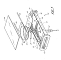
- FIG. 10 there is illustrated an elongated generally flat rectangular chamber 10 made of quartz.
- the chamber includes a flat upper wall 10a, a flat lower wall 10b joined by a pair of short vertical side walls 10c.
- a thickened inlet flange 12 extends across the gas inlet end of the chamber attached to the chamber walls.
- a similar gas outlet flange 14 is shown on the downstream end of the chamber attached to the chamber walls.
- the chamber is divided into an upper section 15 and a lower section 17 by a flat front or upstream divider plate 16 and a rear, downstream plate 18 extending between the chamber side walls 10c, generally parallel to the upper and lower walls.
- the divider plates 16 and 18 are supported by supports 19 formed on the side walls 10c, or by supports (not shown) extending upwardly from the chamber bottom wall.
- the rear chamber divider plate is in approximately the same plane as the front plate.
- the chamber is further divided by a generally flat circular susceptor 20 and a surrounding ring 22, sometimes referred to as a temperature compensation ring or a slip ring (to prevent crystallographic slip).
- a temperature compensation ring or a slip ring to prevent crystallographic slip.
- the optimum slip ring and thermal mass may be somewhat larger or smaller than that of the susceptor. Experimentation is suitable to identify the optimum.
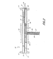
- the susceptor and the slip ring are also positioned in substantially the same plane as the divider plates 18 and 16, as best seen in the cross-sectional view of Figure 2.
- the susceptor 20 is supported by a spider 24 having three arms extending radially outwardly from a central hub and having upwardly extending projections on the ends of the arms engaging the susceptor.
- the susceptor may also be provided with one or more recesses (not shown) on its lower surface for receiving the ends of the projections so as to centrally position the susceptor and to form a coupling for rotating the susceptor.
- the spider is mounted on a schematically shown tubular shaft 26 which extends through the chamber lower wall 10b and also extends through a quartz tube 27 attached to and depending from the lower chamber wall.
- the shaft is adapted to be connected to a drive (not shown) for rotating the shaft, the spider and the susceptor.
- a getter plate 30 Positioned downstream from the susceptor and the ring is a getter plate 30 supported on a plurality of pins 31 extending upwardly from the rear chamber divider plate 18.
- the getter plate extends generally parallel to and approximately mid-way between the upper chamber wall 10a and the divider plate.
- One or more of these plates could be used.
- the plate can be shaped to tailor the gas flow dynamics of the system. Acceptable results have been obtained with a single flat plate. However, to someone skilled in the art, the optimization of the shape of the plate is straight forward.
- shields or heat absorbers 32 are also optionally positioned downstream from the susceptor positioned downstream from the susceptor.
- shields or heat absorbers 33 may be employed on each side of the central area of the chamber adjacent the central portions of the side walls 10c.
- the elements 33 may not be needed because the silicon carbide ring 22 adjacent the chamber walls has considerable heating effect on these adjacent chamber walls.
- These elements 32 and 33 may be held in position by any suitable means.
- the elements 32 might be positioned by the pins 31, and spaced slightly from the chamber side walls 10c.
- projections may be mounted on the chamber side walls and on the downstream plate 18 to position the elements 32 slightly spaced from the side walls.
- the elements 33 may rest on supports on the chamber lower wall 10b between the chamber side walls 10c and the stand 23 positioned by suitable supports mounted on the side walls to space the upper end of the element 33 slightly from the side walls.
- the elements 32 and 33 are preferably made of silicon carbide, or graphite coated with silicon carbide, or other suitable heat-absorbing material.
- the purpose of the elements 32 and 33 is to absorb some heat to minimize the deposition of materials on the chamber walls. Reduced deposition means reduced particle problems due to flaking of coatings on the chamber wall. Further, doping of wafers as the result of leftover dopant and deposits on the chamber is minimized. Also, blockages of radiant heat affecting wafer temperature directly by way of a temperature control loop are also minimized.
- the elements 32 and 33 are illustrated as thin plates that are somewhat co-extensive with the adjacent side walls, other configurations may be employed.
- thicker but vertically shorter elements could be employed in that the elements are primarily heat absorbers and then reradiators of heat to the side walls thus minimize cooling in the chamber edges.
- the shorter, thicker portions would also tend to increase the temperature of the adjacent chamber walls even though they are not co-extensive with the wall.
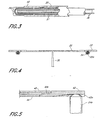
- Figure 7a schematically illustrates a series of silicon carbide pieces 62 adjacent the side wall 63 of a CVD chamber having a generally circular configuration.
- a series of short, straight pieces 62 are illustrated, but of course longer curved portions 64 can be utilized such as in Figure 7b.
- These pieces 62 are supported in a suitable manner adjacent to the side chamber wall such as on suitable quartz pins (not shown) supported on a quartz chamber flange 65.
- Figure 7b schematically illustrates a chamber having a dome shaped upper wall 66.
- a cleaner chamber of course leads to better process results for the reasons mentioned above. Further, a cleaner chamber does not have to be pulled as frequently thus less downtime, and a chamber which has to be cleaned less frequently will last longer because of the reduced wear caused by the cleaning process.
- thermocouples 34 are shown on opposite sides of the ring 22, with the thermocouples extending generally parallel to the chamber side walls 10c.
- the thermocouples are positioned beneath and supported by the ring 22, as best seen in Figure 4, which shows each thermocouple extending through a tubular portion 22a of the ring.
- each thermocouple 34 includes an outer sheath 35 surrounding a ceramic support 37 that has a pair of thermocouple wires 36 extending therethrough and forming a junction 36a.
- a small quartz sleeve or cap 40 extends over the thermocouple junction 36a to shield it from the sheath, in the event the sheath is not chemically compatible with the thermocouple wires.
- a boron nitride coating can be used on the wires.
- thermocouple junction 36a is located at each of the forward or upstream corners of the ring 22. Also, it is desirable that one or two additional thermocouple junctions be positioned in each sheath 35, with the junction of a second pair of wires being located adjacent the rear or downstream corners of the ring 22. Also, a junction could be located between the upstream and downstream corners.
- a similar thermocouple 38 is shown extending upwardly through the tubular shaft 26, with its tip located close to the center of the susceptor 20.
- Both the susceptor and the surrounding ring are formed to have a very low thermal mass.
- the susceptor has mass comparable to that of a semiconductor wafer which it is to support, say within a factor of three.
- the susceptor may be formed as one piece as shown in Figure 4 or as two pieces as shown in Figure 5.
- This includes an outer support ring 42 having a lower inwardly extending flange supporting a central flat disc 44.
- the ring further includes an edge having three to six raised lips 42b for supporting a wafer 45 that fits within the ring 42. The lips space the wafer from the disc 44.
- the end of one spider arm projection 24a is shown positioned in a groove 42a in the lower surface of the ring 42.
- the susceptor, the ring and the getter plate are all made from a material which can withstand the CVD processing as well or better than that of SiC coated graphite.
- the thermocouple sheaths are made from a material which does not devitrify.
- the material should be a good absorber of radiant energy from the susceptor and the heating lamps 46, schematically illustrated in Figure 2. Further, the material must be a reasonably good thermal conductor and be able to withstand the high temperatures encountered in CVD processing over a large number of cycles. This also includes the ability to withstand the thermal shock that repeatedly occurs with the placing of a relatively cold wafer on a hot susceptor.
- the material must be durable and compatible with the various materials employed in the deposition process, as well as, the various chemicals employed in cleaning or etching, and it must have excellent chemical stability.
- the prime material meeting those qualifications in chemistries typically used for Si or Si-Ge epitaxy is silicon carbide.
- the susceptor and its surrounding ring are preferably made of solid silicon carbide as opposed to the prior art approach of using graphite coated with silicon carbide.
- the ring and the susceptor as well as the getter plate and the thermocouple sheaths are preferably formed of CVD silicon carbide. This enables the susceptor and the ring to be used through many more heating cycles than the previously used silicon carbide coated graphite components. Since the temperature downstream of the susceptor is less than on the susceptor, the getter device may last longer than the other elements of the system.
- the silicon carbide thermocouple sheath can withstand many more cycles than the previously used quartz sheaths.
- the life of the reactor components is also improved by providing shields of silicon carbide at specific locations throughout the chamber. Deposition of material on quartz pieces (like Si) can lead to premature failure of the quartz. Shielding critical areas with SiC prevents deterioration of the quartz, thereby extending the life of the process chamber. It will be appreciated that silicon carbide shields may be provided wherever quartz is found in the chamber, such as the spider 24, the stand 23, thermocouples 34 and 38, and any other suitable locations, so long as the silicon carbide does not substantially interfere with the operation of the chamber.
- thermocouple 38 comprises thermocouple wires 50 surrounded by a quartz sheath 52.
- a silicon carbide cap 54 is provided over the quartz sheath 52 to protect the thermocouple 38 from processing gases that tend to deposit on the tip of thermocouple, and to insulate the quartz sheath from the effects of the etch process which is used to remove the process gas deposits.
- Silicon carbide shields such as the cap 54 shown in Figure 6 are preferably formed from a simple geometric construction adapted to fit over the corresponding quartz component to isolate the component either partially or fully from the processing gases of the chamber. Because silicon carbide components are generally relatively expensive and difficult to form into complex shapes, the use of simple geometries, such as caps, flat plates, L-shapes, U-shapes, T-shapes and various other planar, curved and curviplanar shapes, minimizes the cost of manufacture and simplifies the overall manufacturing process. This further enables the complex components of the chamber to be formed from quartz, which is relatively inexpensive and easy to machine and weld. Thus, in the chamber 10 illustrated in the preferred embodiment of Figures 1 and 2, components such as the thermocouples 34 and 38, the spider 24 and the stand 23 are preferably manufactured using quartz and are then capped with a simply constructed silicon carbide shield.
- silicon carbide In addition to silicon carbide, other materials that may be satisfactory are boron nitride, silicon nitride, silicon dioxide, aluminum nitride, aluminum oxide, combinations or ternary compounds or quaternary compounds of these materials, pyrolytic graphite and other similar high temperature ceramic compounds.
- the silicon carbide components may be made by a combination of CVD of SiC and material removal techniques. Examples of such techniques are discussed in U.S. Patents 4,978,567 and 5,514,439 incorporated herein by reference.
- two gas flows are introduced into the reactor.
- the flow of reactants is introduced through the inlet flange 12 to cause the growth of silicon or other material on a wafer positioned within a central recess in the upper surface of the susceptor.
- a purge gas is introduced through the inlet flange to keep reactant gases or cleaning gas from flowing into the bottom part of the reactor through the small gaps between the ring and the divider plates and between the susceptor and the ring.
- the downstream end of the lower chamber region is blocked by a plug or wall 48 so that the purge gas is forced to leak through the gaps to the upper chamber outlet, thereby minimizing the possibility of gas from the upper chamber flowing into the lower one.
- Unused reactants flowing downstream from the susceptor and ring are deposited on both sides of the getter plate of Figure 1, thereby minimizing deposition on the upper quartz wall of the reactor.
- the getter plate in addition to receiving deposition itself, reradiates energy towards the cooler upper chamber wall, including energy in a wave length range in which a significant portion will be absorbed by the quartz wall.
- the pieces positioned against the side wall work in similar fashion. It should be noted that it is important to position those elements close to the surface desired to be heated to maximize the radiation being absorbed.
- the silicon carbide pieces are located so as to heat the surrounding side chamber wall and the peripheral portion of the upper dome wall 66.
- gas flow can be downwardly from the center of an upper chamber wall or can be horizontally across the chamber.
- a horizontally wide but vertically short slot (not shown) is formed in the side wall of the chamber, and there would be no need or desire to have the silicon carbide pieces in that area, but they are desirable around the remainder of the periphery of the chamber side wall including adjacent a gas outlet slot (not shown). Maintaining the chamber warm during a chamber cleaning cycle also maximizes the etch efficiency of a cleaning agent, such as Hcl.
- the life of the process chamber is significantly extended, estimated to increase from about 10,000 wafers to more than about 20,000 wafers. Further, by protecting the components in the lower portion of the chamber, the quartz spider and the quartz stand for the ring also have extended life and need not be replaced any more frequently than the chamber itself. Further, it is possible that silicon carbide or other mentioned materials could be used for those components.
- the susceptor, surrounding ring and the thermocouple sheaths are also manufactured from solid silicon carbide, like the downstream getter plate.
- Solid silicon carbide is not appreciably attacked by an Hcl chamber etch at high temperatures.
- the life of solid silicon carbide components is estimated to be about 20,000 wafers which is about five times that of silicon carbide coated graphite components (about 3,000 to 4,000 wafers). This balances the life of the light absorbing susceptor and ring with that of the reactor chamber.
- the thermocouple sheaths will last approximately that long, or longer. Consequently, the improvements in lifetime of the internal reactor components and quartz chamber can improve the maintenance frequency on the reactor from a maximum of about 1,500 to 4,000 wafers to about 20,000 wafers.
Landscapes
- Chemical & Material Sciences (AREA)
- Engineering & Computer Science (AREA)
- Chemical Kinetics & Catalysis (AREA)
- Organic Chemistry (AREA)
- Metallurgy (AREA)
- Mechanical Engineering (AREA)
- Materials Engineering (AREA)
- General Chemical & Material Sciences (AREA)
- Physics & Mathematics (AREA)
- General Physics & Mathematics (AREA)
- Toxicology (AREA)
- Health & Medical Sciences (AREA)
- Condensed Matter Physics & Semiconductors (AREA)
- Power Engineering (AREA)
- Microelectronics & Electronic Packaging (AREA)
- Computer Hardware Design (AREA)
- Manufacturing & Machinery (AREA)
- Chemical Vapour Deposition (AREA)
- Measuring Temperature Or Quantity Of Heat (AREA)
Applications Claiming Priority (5)
| Application Number | Priority Date | Filing Date | Title |
|---|---|---|---|
| US6456797P | 1997-11-03 | 1997-11-03 | |
| US64567P | 1997-11-03 | ||
| US9513998P | 1998-07-31 | 1998-07-31 | |
| US95139P | 1998-07-31 | ||
| PCT/US1998/023205 WO1999023276A1 (en) | 1997-11-03 | 1998-11-02 | Long life high temperature process chamber |
Publications (2)
| Publication Number | Publication Date |
|---|---|
| EP1029109A1 EP1029109A1 (en) | 2000-08-23 |
| EP1029109B1 true EP1029109B1 (en) | 2007-09-26 |
Family
ID=26744648
Family Applications (1)
| Application Number | Title | Priority Date | Filing Date |
|---|---|---|---|
| EP98957469A Expired - Lifetime EP1029109B1 (en) | 1997-11-03 | 1998-11-02 | Long life high temperature process chamber |
Country Status (6)
| Country | Link |
|---|---|
| US (1) | US6325858B1 (enExample) |
| EP (1) | EP1029109B1 (enExample) |
| JP (1) | JP4475804B2 (enExample) |
| KR (1) | KR20010031714A (enExample) |
| DE (1) | DE69838484T2 (enExample) |
| WO (1) | WO1999023276A1 (enExample) |
Cited By (1)
| Publication number | Priority date | Publication date | Assignee | Title |
|---|---|---|---|---|
| US8033772B2 (en) | 2002-06-21 | 2011-10-11 | Applied Materials, Inc. | Transfer chamber for vacuum processing system |
Families Citing this family (446)
| Publication number | Priority date | Publication date | Assignee | Title |
|---|---|---|---|---|
| US6093252A (en) | 1995-08-03 | 2000-07-25 | Asm America, Inc. | Process chamber with inner support |
| US6113702A (en) * | 1995-09-01 | 2000-09-05 | Asm America, Inc. | Wafer support system |
| US6530994B1 (en) * | 1997-08-15 | 2003-03-11 | Micro C Technologies, Inc. | Platform for supporting a semiconductor substrate and method of supporting a substrate during rapid high temperature processing |
| NL1012004C2 (nl) * | 1999-05-07 | 2000-11-13 | Asm Int | Werkwijze voor het verplaatsen van wafers alsmede ring. |
| US6169244B1 (en) | 1999-05-21 | 2001-01-02 | Moore Epitaxial, Inc. | Thermocouple sheath cover |
| US6315833B1 (en) * | 1999-07-01 | 2001-11-13 | Applied Materials, Inc. | Silicon carbide sleeve for substrate support assembly |
| JP3438665B2 (ja) | 1999-09-02 | 2003-08-18 | 信越半導体株式会社 | 熱処理装置 |
| KR100752682B1 (ko) * | 2000-04-06 | 2007-08-29 | 에이에스엠 아메리카, 인코포레이티드 | 유리질 보호용 장벽코팅 |
| US7163587B2 (en) * | 2002-02-08 | 2007-01-16 | Axcelis Technologies, Inc. | Reactor assembly and processing method |
| US6796711B2 (en) * | 2002-03-29 | 2004-09-28 | Axcelis Technologies, Inc. | Contact temperature probe and process |
| US7122844B2 (en) * | 2002-05-13 | 2006-10-17 | Cree, Inc. | Susceptor for MOCVD reactor |
| US6825051B2 (en) | 2002-05-17 | 2004-11-30 | Asm America, Inc. | Plasma etch resistant coating and process |
| US8366830B2 (en) * | 2003-03-04 | 2013-02-05 | Cree, Inc. | Susceptor apparatus for inverted type MOCVD reactor |
| US6974781B2 (en) | 2003-10-20 | 2005-12-13 | Asm International N.V. | Reactor precoating for reduced stress and uniform CVD |
| JP2005229043A (ja) * | 2004-02-16 | 2005-08-25 | Sumitomo Electric Ind Ltd | ヒータユニット及び該ヒータを搭載した装置 |
| US9612215B2 (en) * | 2004-07-22 | 2017-04-04 | Toyo Tanso Co., Ltd. | Susceptor |
| US20060093756A1 (en) * | 2004-11-03 | 2006-05-04 | Nagarajan Rajagopalan | High-power dielectric seasoning for stable wafer-to-wafer thickness uniformity of dielectric CVD films |
| US20060275933A1 (en) * | 2005-06-02 | 2006-12-07 | Applied Materials, Inc. | Thermally conductive ceramic tipped contact thermocouple |
| US20070089836A1 (en) * | 2005-10-24 | 2007-04-26 | Applied Materials, Inc. | Semiconductor process chamber |
| DE102006055038B4 (de) | 2006-11-22 | 2012-12-27 | Siltronic Ag | Epitaxierte Halbleiterscheibe sowie Vorrichtung und Verfahren zur Herstellung einer epitaxierten Halbleiterscheibe |
| US7874726B2 (en) * | 2007-05-24 | 2011-01-25 | Asm America, Inc. | Thermocouple |
| US8034410B2 (en) | 2007-07-17 | 2011-10-11 | Asm International N.V. | Protective inserts to line holes in parts for semiconductor process equipment |
| US20090052498A1 (en) * | 2007-08-24 | 2009-02-26 | Asm America, Inc. | Thermocouple |
| US7807222B2 (en) * | 2007-09-17 | 2010-10-05 | Asm International N.V. | Semiconductor processing parts having apertures with deposited coatings and methods for forming the same |
| US20110114022A1 (en) * | 2007-12-12 | 2011-05-19 | Veeco Instruments Inc. | Wafer carrier with hub |
| US7993057B2 (en) * | 2007-12-20 | 2011-08-09 | Asm America, Inc. | Redundant temperature sensor for semiconductor processing chambers |
| US8388755B2 (en) * | 2008-02-27 | 2013-03-05 | Soitec | Thermalization of gaseous precursors in CVD reactors |
| US7946762B2 (en) * | 2008-06-17 | 2011-05-24 | Asm America, Inc. | Thermocouple |
| DE102008034260B4 (de) | 2008-07-16 | 2014-06-26 | Siltronic Ag | Verfahren zum Abscheiden einer Schicht auf einer Halbleiterscheibe mittels CVD in einer Kammer und Kammer zum Abscheiden einer Schicht auf einer Halbleiterscheibe mittels CVD |
| US8394229B2 (en) * | 2008-08-07 | 2013-03-12 | Asm America, Inc. | Susceptor ring |
| US8801857B2 (en) * | 2008-10-31 | 2014-08-12 | Asm America, Inc. | Self-centering susceptor ring assembly |
| CN102203910B (zh) * | 2008-11-07 | 2014-12-10 | Asm美国公司 | 反应室 |
| US10378106B2 (en) | 2008-11-14 | 2019-08-13 | Asm Ip Holding B.V. | Method of forming insulation film by modified PEALD |
| US8262287B2 (en) | 2008-12-08 | 2012-09-11 | Asm America, Inc. | Thermocouple |
| US9394608B2 (en) | 2009-04-06 | 2016-07-19 | Asm America, Inc. | Semiconductor processing reactor and components thereof |
| US8100583B2 (en) * | 2009-05-06 | 2012-01-24 | Asm America, Inc. | Thermocouple |
| US9297705B2 (en) | 2009-05-06 | 2016-03-29 | Asm America, Inc. | Smart temperature measuring device |
| US8382370B2 (en) | 2009-05-06 | 2013-02-26 | Asm America, Inc. | Thermocouple assembly with guarded thermocouple junction |
| US8802201B2 (en) | 2009-08-14 | 2014-08-12 | Asm America, Inc. | Systems and methods for thin-film deposition of metal oxides using excited nitrogen-oxygen species |
| JP2011054870A (ja) * | 2009-09-04 | 2011-03-17 | Shin Etsu Handotai Co Ltd | 気相成長装置及びシリコンエピタキシャルウェーハの製造方法 |
| US9312155B2 (en) | 2011-06-06 | 2016-04-12 | Asm Japan K.K. | High-throughput semiconductor-processing apparatus equipped with multiple dual-chamber modules |
| NL2008751A (en) * | 2011-06-06 | 2012-12-10 | Asml Netherlands Bv | Temperature sensing probe, burl plate, lithographic apparatus and method. |
| JP5878813B2 (ja) * | 2011-06-21 | 2016-03-08 | 東京エレクトロン株式会社 | バッチ式処理装置 |
| US9793148B2 (en) | 2011-06-22 | 2017-10-17 | Asm Japan K.K. | Method for positioning wafers in multiple wafer transport |
| US10364496B2 (en) | 2011-06-27 | 2019-07-30 | Asm Ip Holding B.V. | Dual section module having shared and unshared mass flow controllers |
| US10854498B2 (en) | 2011-07-15 | 2020-12-01 | Asm Ip Holding B.V. | Wafer-supporting device and method for producing same |
| US20130023129A1 (en) | 2011-07-20 | 2013-01-24 | Asm America, Inc. | Pressure transmitter for a semiconductor processing environment |
| US9017481B1 (en) | 2011-10-28 | 2015-04-28 | Asm America, Inc. | Process feed management for semiconductor substrate processing |
| US8946830B2 (en) | 2012-04-04 | 2015-02-03 | Asm Ip Holdings B.V. | Metal oxide protective layer for a semiconductor device |
| US9558931B2 (en) | 2012-07-27 | 2017-01-31 | Asm Ip Holding B.V. | System and method for gas-phase sulfur passivation of a semiconductor surface |
| US9659799B2 (en) | 2012-08-28 | 2017-05-23 | Asm Ip Holding B.V. | Systems and methods for dynamic semiconductor process scheduling |
| US9021985B2 (en) | 2012-09-12 | 2015-05-05 | Asm Ip Holdings B.V. | Process gas management for an inductively-coupled plasma deposition reactor |
| US10714315B2 (en) | 2012-10-12 | 2020-07-14 | Asm Ip Holdings B.V. | Semiconductor reaction chamber showerhead |
| US9640416B2 (en) | 2012-12-26 | 2017-05-02 | Asm Ip Holding B.V. | Single-and dual-chamber module-attachable wafer-handling chamber |
| US20160376700A1 (en) | 2013-02-01 | 2016-12-29 | Asm Ip Holding B.V. | System for treatment of deposition reactor |
| USD702188S1 (en) | 2013-03-08 | 2014-04-08 | Asm Ip Holding B.V. | Thermocouple |
| US9484191B2 (en) | 2013-03-08 | 2016-11-01 | Asm Ip Holding B.V. | Pulsed remote plasma method and system |
| US9589770B2 (en) | 2013-03-08 | 2017-03-07 | Asm Ip Holding B.V. | Method and systems for in-situ formation of intermediate reactive species |
| US8993054B2 (en) | 2013-07-12 | 2015-03-31 | Asm Ip Holding B.V. | Method and system to reduce outgassing in a reaction chamber |
| US9018111B2 (en) | 2013-07-22 | 2015-04-28 | Asm Ip Holding B.V. | Semiconductor reaction chamber with plasma capabilities |
| US9793115B2 (en) | 2013-08-14 | 2017-10-17 | Asm Ip Holding B.V. | Structures and devices including germanium-tin films and methods of forming same |
| US9240412B2 (en) | 2013-09-27 | 2016-01-19 | Asm Ip Holding B.V. | Semiconductor structure and device and methods of forming same using selective epitaxial process |
| US9556516B2 (en) | 2013-10-09 | 2017-01-31 | ASM IP Holding B.V | Method for forming Ti-containing film by PEALD using TDMAT or TDEAT |
| US9605343B2 (en) | 2013-11-13 | 2017-03-28 | Asm Ip Holding B.V. | Method for forming conformal carbon films, structures conformal carbon film, and system of forming same |
| US10179947B2 (en) | 2013-11-26 | 2019-01-15 | Asm Ip Holding B.V. | Method for forming conformal nitrided, oxidized, or carbonized dielectric film by atomic layer deposition |
| US10683571B2 (en) | 2014-02-25 | 2020-06-16 | Asm Ip Holding B.V. | Gas supply manifold and method of supplying gases to chamber using same |
| US10167557B2 (en) | 2014-03-18 | 2019-01-01 | Asm Ip Holding B.V. | Gas distribution system, reactor including the system, and methods of using the same |
| US9447498B2 (en) | 2014-03-18 | 2016-09-20 | Asm Ip Holding B.V. | Method for performing uniform processing in gas system-sharing multiple reaction chambers |
| US11015245B2 (en) | 2014-03-19 | 2021-05-25 | Asm Ip Holding B.V. | Gas-phase reactor and system having exhaust plenum and components thereof |
| US9349620B2 (en) * | 2014-07-09 | 2016-05-24 | Asm Ip Holdings B.V. | Apparatus and method for pre-baking substrate upstream of process chamber |
| US10858737B2 (en) | 2014-07-28 | 2020-12-08 | Asm Ip Holding B.V. | Showerhead assembly and components thereof |
| US9543180B2 (en) | 2014-08-01 | 2017-01-10 | Asm Ip Holding B.V. | Apparatus and method for transporting wafers between wafer carrier and process tool under vacuum |
| US9890456B2 (en) | 2014-08-21 | 2018-02-13 | Asm Ip Holding B.V. | Method and system for in situ formation of gas-phase compounds |
| US9657845B2 (en) | 2014-10-07 | 2017-05-23 | Asm Ip Holding B.V. | Variable conductance gas distribution apparatus and method |
| US10941490B2 (en) | 2014-10-07 | 2021-03-09 | Asm Ip Holding B.V. | Multiple temperature range susceptor, assembly, reactor and system including the susceptor, and methods of using the same |
| KR102300403B1 (ko) | 2014-11-19 | 2021-09-09 | 에이에스엠 아이피 홀딩 비.브이. | 박막 증착 방법 |
| KR102263121B1 (ko) | 2014-12-22 | 2021-06-09 | 에이에스엠 아이피 홀딩 비.브이. | 반도체 소자 및 그 제조 방법 |
| US9478415B2 (en) | 2015-02-13 | 2016-10-25 | Asm Ip Holding B.V. | Method for forming film having low resistance and shallow junction depth |
| US10529542B2 (en) | 2015-03-11 | 2020-01-07 | Asm Ip Holdings B.V. | Cross-flow reactor and method |
| US10276355B2 (en) | 2015-03-12 | 2019-04-30 | Asm Ip Holding B.V. | Multi-zone reactor, system including the reactor, and method of using the same |
| CN104818527A (zh) * | 2015-04-08 | 2015-08-05 | 上海晶盟硅材料有限公司 | 外延片生产设备 |
| US10458018B2 (en) | 2015-06-26 | 2019-10-29 | Asm Ip Holding B.V. | Structures including metal carbide material, devices including the structures, and methods of forming same |
| US10600673B2 (en) | 2015-07-07 | 2020-03-24 | Asm Ip Holding B.V. | Magnetic susceptor to baseplate seal |
| CN106338423B (zh) | 2015-07-10 | 2020-07-14 | 三斯坎公司 | 组织学染色的空间复用 |
| US9899291B2 (en) | 2015-07-13 | 2018-02-20 | Asm Ip Holding B.V. | Method for protecting layer by forming hydrocarbon-based extremely thin film |
| US10043661B2 (en) | 2015-07-13 | 2018-08-07 | Asm Ip Holding B.V. | Method for protecting layer by forming hydrocarbon-based extremely thin film |
| US10083836B2 (en) | 2015-07-24 | 2018-09-25 | Asm Ip Holding B.V. | Formation of boron-doped titanium metal films with high work function |
| US10087525B2 (en) | 2015-08-04 | 2018-10-02 | Asm Ip Holding B.V. | Variable gap hard stop design |
| US9647114B2 (en) | 2015-08-14 | 2017-05-09 | Asm Ip Holding B.V. | Methods of forming highly p-type doped germanium tin films and structures and devices including the films |
| US9711345B2 (en) | 2015-08-25 | 2017-07-18 | Asm Ip Holding B.V. | Method for forming aluminum nitride-based film by PEALD |
| US9960072B2 (en) | 2015-09-29 | 2018-05-01 | Asm Ip Holding B.V. | Variable adjustment for precise matching of multiple chamber cavity housings |
| US9909214B2 (en) | 2015-10-15 | 2018-03-06 | Asm Ip Holding B.V. | Method for depositing dielectric film in trenches by PEALD |
| US10211308B2 (en) | 2015-10-21 | 2019-02-19 | Asm Ip Holding B.V. | NbMC layers |
| US10322384B2 (en) | 2015-11-09 | 2019-06-18 | Asm Ip Holding B.V. | Counter flow mixer for process chamber |
| US9455138B1 (en) | 2015-11-10 | 2016-09-27 | Asm Ip Holding B.V. | Method for forming dielectric film in trenches by PEALD using H-containing gas |
| US9905420B2 (en) | 2015-12-01 | 2018-02-27 | Asm Ip Holding B.V. | Methods of forming silicon germanium tin films and structures and devices including the films |
| US9607837B1 (en) | 2015-12-21 | 2017-03-28 | Asm Ip Holding B.V. | Method for forming silicon oxide cap layer for solid state diffusion process |
| US9735024B2 (en) | 2015-12-28 | 2017-08-15 | Asm Ip Holding B.V. | Method of atomic layer etching using functional group-containing fluorocarbon |
| US9627221B1 (en) | 2015-12-28 | 2017-04-18 | Asm Ip Holding B.V. | Continuous process incorporating atomic layer etching |
| US11139308B2 (en) | 2015-12-29 | 2021-10-05 | Asm Ip Holding B.V. | Atomic layer deposition of III-V compounds to form V-NAND devices |
| DE102016101003A1 (de) | 2016-01-21 | 2017-07-27 | Aixtron Se | CVD-Vorrichtung mit einem als Baugruppe aus dem Reaktorgehäuse entnehmbaren Prozesskammergehäuse |
| US10468251B2 (en) | 2016-02-19 | 2019-11-05 | Asm Ip Holding B.V. | Method for forming spacers using silicon nitride film for spacer-defined multiple patterning |
| US9754779B1 (en) | 2016-02-19 | 2017-09-05 | Asm Ip Holding B.V. | Method for forming silicon nitride film selectively on sidewalls or flat surfaces of trenches |
| US10529554B2 (en) | 2016-02-19 | 2020-01-07 | Asm Ip Holding B.V. | Method for forming silicon nitride film selectively on sidewalls or flat surfaces of trenches |
| US10501866B2 (en) | 2016-03-09 | 2019-12-10 | Asm Ip Holding B.V. | Gas distribution apparatus for improved film uniformity in an epitaxial system |
| US10343920B2 (en) | 2016-03-18 | 2019-07-09 | Asm Ip Holding B.V. | Aligned carbon nanotubes |
| US9892913B2 (en) | 2016-03-24 | 2018-02-13 | Asm Ip Holding B.V. | Radial and thickness control via biased multi-port injection settings |
| US10190213B2 (en) | 2016-04-21 | 2019-01-29 | Asm Ip Holding B.V. | Deposition of metal borides |
| US10087522B2 (en) | 2016-04-21 | 2018-10-02 | Asm Ip Holding B.V. | Deposition of metal borides |
| US10865475B2 (en) | 2016-04-21 | 2020-12-15 | Asm Ip Holding B.V. | Deposition of metal borides and silicides |
| US10367080B2 (en) | 2016-05-02 | 2019-07-30 | Asm Ip Holding B.V. | Method of forming a germanium oxynitride film |
| US10032628B2 (en) | 2016-05-02 | 2018-07-24 | Asm Ip Holding B.V. | Source/drain performance through conformal solid state doping |
| KR102592471B1 (ko) | 2016-05-17 | 2023-10-20 | 에이에스엠 아이피 홀딩 비.브이. | 금속 배선 형성 방법 및 이를 이용한 반도체 장치의 제조 방법 |
| US11453943B2 (en) | 2016-05-25 | 2022-09-27 | Asm Ip Holding B.V. | Method for forming carbon-containing silicon/metal oxide or nitride film by ALD using silicon precursor and hydrocarbon precursor |
| US10388509B2 (en) | 2016-06-28 | 2019-08-20 | Asm Ip Holding B.V. | Formation of epitaxial layers via dislocation filtering |
| US10612137B2 (en) | 2016-07-08 | 2020-04-07 | Asm Ip Holdings B.V. | Organic reactants for atomic layer deposition |
| US9859151B1 (en) | 2016-07-08 | 2018-01-02 | Asm Ip Holding B.V. | Selective film deposition method to form air gaps |
| US9793135B1 (en) | 2016-07-14 | 2017-10-17 | ASM IP Holding B.V | Method of cyclic dry etching using etchant film |
| US10714385B2 (en) | 2016-07-19 | 2020-07-14 | Asm Ip Holding B.V. | Selective deposition of tungsten |
| KR102354490B1 (ko) | 2016-07-27 | 2022-01-21 | 에이에스엠 아이피 홀딩 비.브이. | 기판 처리 방법 |
| US10395919B2 (en) | 2016-07-28 | 2019-08-27 | Asm Ip Holding B.V. | Method and apparatus for filling a gap |
| US10177025B2 (en) | 2016-07-28 | 2019-01-08 | Asm Ip Holding B.V. | Method and apparatus for filling a gap |
| US9887082B1 (en) | 2016-07-28 | 2018-02-06 | Asm Ip Holding B.V. | Method and apparatus for filling a gap |
| US9812320B1 (en) | 2016-07-28 | 2017-11-07 | Asm Ip Holding B.V. | Method and apparatus for filling a gap |
| KR102532607B1 (ko) | 2016-07-28 | 2023-05-15 | 에이에스엠 아이피 홀딩 비.브이. | 기판 가공 장치 및 그 동작 방법 |
| US10090316B2 (en) | 2016-09-01 | 2018-10-02 | Asm Ip Holding B.V. | 3D stacked multilayer semiconductor memory using doped select transistor channel |
| US10410943B2 (en) | 2016-10-13 | 2019-09-10 | Asm Ip Holding B.V. | Method for passivating a surface of a semiconductor and related systems |
| US10643826B2 (en) | 2016-10-26 | 2020-05-05 | Asm Ip Holdings B.V. | Methods for thermally calibrating reaction chambers |
| US11532757B2 (en) | 2016-10-27 | 2022-12-20 | Asm Ip Holding B.V. | Deposition of charge trapping layers |
| US10714350B2 (en) | 2016-11-01 | 2020-07-14 | ASM IP Holdings, B.V. | Methods for forming a transition metal niobium nitride film on a substrate by atomic layer deposition and related semiconductor device structures |
| US10229833B2 (en) | 2016-11-01 | 2019-03-12 | Asm Ip Holding B.V. | Methods for forming a transition metal nitride film on a substrate by atomic layer deposition and related semiconductor device structures |
| US10435790B2 (en) | 2016-11-01 | 2019-10-08 | Asm Ip Holding B.V. | Method of subatmospheric plasma-enhanced ALD using capacitively coupled electrodes with narrow gap |
| US10643904B2 (en) | 2016-11-01 | 2020-05-05 | Asm Ip Holdings B.V. | Methods for forming a semiconductor device and related semiconductor device structures |
| US10134757B2 (en) | 2016-11-07 | 2018-11-20 | Asm Ip Holding B.V. | Method of processing a substrate and a device manufactured by using the method |
| KR102546317B1 (ko) | 2016-11-15 | 2023-06-21 | 에이에스엠 아이피 홀딩 비.브이. | 기체 공급 유닛 및 이를 포함하는 기판 처리 장치 |
| US10340135B2 (en) | 2016-11-28 | 2019-07-02 | Asm Ip Holding B.V. | Method of topologically restricted plasma-enhanced cyclic deposition of silicon or metal nitride |
| KR102762543B1 (ko) | 2016-12-14 | 2025-02-05 | 에이에스엠 아이피 홀딩 비.브이. | 기판 처리 장치 |
| US11447861B2 (en) | 2016-12-15 | 2022-09-20 | Asm Ip Holding B.V. | Sequential infiltration synthesis apparatus and a method of forming a patterned structure |
| US11581186B2 (en) | 2016-12-15 | 2023-02-14 | Asm Ip Holding B.V. | Sequential infiltration synthesis apparatus |
| US9916980B1 (en) | 2016-12-15 | 2018-03-13 | Asm Ip Holding B.V. | Method of forming a structure on a substrate |
| KR102700194B1 (ko) | 2016-12-19 | 2024-08-28 | 에이에스엠 아이피 홀딩 비.브이. | 기판 처리 장치 |
| US10269558B2 (en) | 2016-12-22 | 2019-04-23 | Asm Ip Holding B.V. | Method of forming a structure on a substrate |
| US10867788B2 (en) | 2016-12-28 | 2020-12-15 | Asm Ip Holding B.V. | Method of forming a structure on a substrate |
| US11390950B2 (en) | 2017-01-10 | 2022-07-19 | Asm Ip Holding B.V. | Reactor system and method to reduce residue buildup during a film deposition process |
| US10655221B2 (en) | 2017-02-09 | 2020-05-19 | Asm Ip Holding B.V. | Method for depositing oxide film by thermal ALD and PEALD |
| US10468261B2 (en) | 2017-02-15 | 2019-11-05 | Asm Ip Holding B.V. | Methods for forming a metallic film on a substrate by cyclical deposition and related semiconductor device structures |
| US10529563B2 (en) | 2017-03-29 | 2020-01-07 | Asm Ip Holdings B.V. | Method for forming doped metal oxide films on a substrate by cyclical deposition and related semiconductor device structures |
| US10283353B2 (en) | 2017-03-29 | 2019-05-07 | Asm Ip Holding B.V. | Method of reforming insulating film deposited on substrate with recess pattern |
| US10103040B1 (en) | 2017-03-31 | 2018-10-16 | Asm Ip Holding B.V. | Apparatus and method for manufacturing a semiconductor device |
| USD830981S1 (en) | 2017-04-07 | 2018-10-16 | Asm Ip Holding B.V. | Susceptor for semiconductor substrate processing apparatus |
| KR102457289B1 (ko) | 2017-04-25 | 2022-10-21 | 에이에스엠 아이피 홀딩 비.브이. | 박막 증착 방법 및 반도체 장치의 제조 방법 |
| US10770286B2 (en) | 2017-05-08 | 2020-09-08 | Asm Ip Holdings B.V. | Methods for selectively forming a silicon nitride film on a substrate and related semiconductor device structures |
| US10892156B2 (en) | 2017-05-08 | 2021-01-12 | Asm Ip Holding B.V. | Methods for forming a silicon nitride film on a substrate and related semiconductor device structures |
| US10446393B2 (en) | 2017-05-08 | 2019-10-15 | Asm Ip Holding B.V. | Methods for forming silicon-containing epitaxial layers and related semiconductor device structures |
| US10504742B2 (en) | 2017-05-31 | 2019-12-10 | Asm Ip Holding B.V. | Method of atomic layer etching using hydrogen plasma |
| US10886123B2 (en) | 2017-06-02 | 2021-01-05 | Asm Ip Holding B.V. | Methods for forming low temperature semiconductor layers and related semiconductor device structures |
| US12040200B2 (en) | 2017-06-20 | 2024-07-16 | Asm Ip Holding B.V. | Semiconductor processing apparatus and methods for calibrating a semiconductor processing apparatus |
| US11306395B2 (en) | 2017-06-28 | 2022-04-19 | Asm Ip Holding B.V. | Methods for depositing a transition metal nitride film on a substrate by atomic layer deposition and related deposition apparatus |
| US10685834B2 (en) | 2017-07-05 | 2020-06-16 | Asm Ip Holdings B.V. | Methods for forming a silicon germanium tin layer and related semiconductor device structures |
| KR20190009245A (ko) | 2017-07-18 | 2019-01-28 | 에이에스엠 아이피 홀딩 비.브이. | 반도체 소자 구조물 형성 방법 및 관련된 반도체 소자 구조물 |
| US11018002B2 (en) | 2017-07-19 | 2021-05-25 | Asm Ip Holding B.V. | Method for selectively depositing a Group IV semiconductor and related semiconductor device structures |
| US11374112B2 (en) | 2017-07-19 | 2022-06-28 | Asm Ip Holding B.V. | Method for depositing a group IV semiconductor and related semiconductor device structures |
| US10541333B2 (en) | 2017-07-19 | 2020-01-21 | Asm Ip Holding B.V. | Method for depositing a group IV semiconductor and related semiconductor device structures |
| US10605530B2 (en) | 2017-07-26 | 2020-03-31 | Asm Ip Holding B.V. | Assembly of a liner and a flange for a vertical furnace as well as the liner and the vertical furnace |
| US10590535B2 (en) | 2017-07-26 | 2020-03-17 | Asm Ip Holdings B.V. | Chemical treatment, deposition and/or infiltration apparatus and method for using the same |
| US10312055B2 (en) | 2017-07-26 | 2019-06-04 | Asm Ip Holding B.V. | Method of depositing film by PEALD using negative bias |
| TWI815813B (zh) | 2017-08-04 | 2023-09-21 | 荷蘭商Asm智慧財產控股公司 | 用於分配反應腔內氣體的噴頭總成 |
| US10770336B2 (en) | 2017-08-08 | 2020-09-08 | Asm Ip Holding B.V. | Substrate lift mechanism and reactor including same |
| US10692741B2 (en) | 2017-08-08 | 2020-06-23 | Asm Ip Holdings B.V. | Radiation shield |
| US10249524B2 (en) | 2017-08-09 | 2019-04-02 | Asm Ip Holding B.V. | Cassette holder assembly for a substrate cassette and holding member for use in such assembly |
| US11139191B2 (en) | 2017-08-09 | 2021-10-05 | Asm Ip Holding B.V. | Storage apparatus for storing cassettes for substrates and processing apparatus equipped therewith |
| US11769682B2 (en) | 2017-08-09 | 2023-09-26 | Asm Ip Holding B.V. | Storage apparatus for storing cassettes for substrates and processing apparatus equipped therewith |
| US10236177B1 (en) | 2017-08-22 | 2019-03-19 | ASM IP Holding B.V.. | Methods for depositing a doped germanium tin semiconductor and related semiconductor device structures |
| USD900036S1 (en) | 2017-08-24 | 2020-10-27 | Asm Ip Holding B.V. | Heater electrical connector and adapter |
| US11830730B2 (en) | 2017-08-29 | 2023-11-28 | Asm Ip Holding B.V. | Layer forming method and apparatus |
| US11295980B2 (en) | 2017-08-30 | 2022-04-05 | Asm Ip Holding B.V. | Methods for depositing a molybdenum metal film over a dielectric surface of a substrate by a cyclical deposition process and related semiconductor device structures |
| KR102491945B1 (ko) | 2017-08-30 | 2023-01-26 | 에이에스엠 아이피 홀딩 비.브이. | 기판 처리 장치 |
| US11056344B2 (en) | 2017-08-30 | 2021-07-06 | Asm Ip Holding B.V. | Layer forming method |
| KR102401446B1 (ko) | 2017-08-31 | 2022-05-24 | 에이에스엠 아이피 홀딩 비.브이. | 기판 처리 장치 |
| US10607895B2 (en) | 2017-09-18 | 2020-03-31 | Asm Ip Holdings B.V. | Method for forming a semiconductor device structure comprising a gate fill metal |
| KR102630301B1 (ko) | 2017-09-21 | 2024-01-29 | 에이에스엠 아이피 홀딩 비.브이. | 침투성 재료의 순차 침투 합성 방법 처리 및 이를 이용하여 형성된 구조물 및 장치 |
| US10844484B2 (en) | 2017-09-22 | 2020-11-24 | Asm Ip Holding B.V. | Apparatus for dispensing a vapor phase reactant to a reaction chamber and related methods |
| US10658205B2 (en) | 2017-09-28 | 2020-05-19 | Asm Ip Holdings B.V. | Chemical dispensing apparatus and methods for dispensing a chemical to a reaction chamber |
| US10403504B2 (en) | 2017-10-05 | 2019-09-03 | Asm Ip Holding B.V. | Method for selectively depositing a metallic film on a substrate |
| US10319588B2 (en) | 2017-10-10 | 2019-06-11 | Asm Ip Holding B.V. | Method for depositing a metal chalcogenide on a substrate by cyclical deposition |
| US10923344B2 (en) | 2017-10-30 | 2021-02-16 | Asm Ip Holding B.V. | Methods for forming a semiconductor structure and related semiconductor structures |
| US10910262B2 (en) | 2017-11-16 | 2021-02-02 | Asm Ip Holding B.V. | Method of selectively depositing a capping layer structure on a semiconductor device structure |
| KR102443047B1 (ko) | 2017-11-16 | 2022-09-14 | 에이에스엠 아이피 홀딩 비.브이. | 기판 처리 장치 방법 및 그에 의해 제조된 장치 |
| US11022879B2 (en) | 2017-11-24 | 2021-06-01 | Asm Ip Holding B.V. | Method of forming an enhanced unexposed photoresist layer |
| TWI791689B (zh) | 2017-11-27 | 2023-02-11 | 荷蘭商Asm智慧財產控股私人有限公司 | 包括潔淨迷你環境之裝置 |
| US11127617B2 (en) | 2017-11-27 | 2021-09-21 | Asm Ip Holding B.V. | Storage device for storing wafer cassettes for use with a batch furnace |
| US10290508B1 (en) | 2017-12-05 | 2019-05-14 | Asm Ip Holding B.V. | Method for forming vertical spacers for spacer-defined patterning |
| US10872771B2 (en) | 2018-01-16 | 2020-12-22 | Asm Ip Holding B. V. | Method for depositing a material film on a substrate within a reaction chamber by a cyclical deposition process and related device structures |
| TWI852426B (zh) | 2018-01-19 | 2024-08-11 | 荷蘭商Asm Ip私人控股有限公司 | 沈積方法 |
| KR102695659B1 (ko) | 2018-01-19 | 2024-08-14 | 에이에스엠 아이피 홀딩 비.브이. | 플라즈마 보조 증착에 의해 갭 충진 층을 증착하는 방법 |
| USD903477S1 (en) | 2018-01-24 | 2020-12-01 | Asm Ip Holdings B.V. | Metal clamp |
| US11018047B2 (en) | 2018-01-25 | 2021-05-25 | Asm Ip Holding B.V. | Hybrid lift pin |
| US10535516B2 (en) | 2018-02-01 | 2020-01-14 | Asm Ip Holdings B.V. | Method for depositing a semiconductor structure on a surface of a substrate and related semiconductor structures |
| USD880437S1 (en) | 2018-02-01 | 2020-04-07 | Asm Ip Holding B.V. | Gas supply plate for semiconductor manufacturing apparatus |
| US11081345B2 (en) | 2018-02-06 | 2021-08-03 | Asm Ip Holding B.V. | Method of post-deposition treatment for silicon oxide film |
| KR102657269B1 (ko) | 2018-02-14 | 2024-04-16 | 에이에스엠 아이피 홀딩 비.브이. | 주기적 증착 공정에 의해 기판 상에 루테늄-함유 막을 증착하는 방법 |
| US10896820B2 (en) | 2018-02-14 | 2021-01-19 | Asm Ip Holding B.V. | Method for depositing a ruthenium-containing film on a substrate by a cyclical deposition process |
| US10731249B2 (en) | 2018-02-15 | 2020-08-04 | Asm Ip Holding B.V. | Method of forming a transition metal containing film on a substrate by a cyclical deposition process, a method for supplying a transition metal halide compound to a reaction chamber, and related vapor deposition apparatus |
| KR102636427B1 (ko) | 2018-02-20 | 2024-02-13 | 에이에스엠 아이피 홀딩 비.브이. | 기판 처리 방법 및 장치 |
| US10658181B2 (en) | 2018-02-20 | 2020-05-19 | Asm Ip Holding B.V. | Method of spacer-defined direct patterning in semiconductor fabrication |
| US10975470B2 (en) | 2018-02-23 | 2021-04-13 | Asm Ip Holding B.V. | Apparatus for detecting or monitoring for a chemical precursor in a high temperature environment |
| US11473195B2 (en) | 2018-03-01 | 2022-10-18 | Asm Ip Holding B.V. | Semiconductor processing apparatus and a method for processing a substrate |
| US11629406B2 (en) | 2018-03-09 | 2023-04-18 | Asm Ip Holding B.V. | Semiconductor processing apparatus comprising one or more pyrometers for measuring a temperature of a substrate during transfer of the substrate |
| US11114283B2 (en) | 2018-03-16 | 2021-09-07 | Asm Ip Holding B.V. | Reactor, system including the reactor, and methods of manufacturing and using same |
| KR102646467B1 (ko) | 2018-03-27 | 2024-03-11 | 에이에스엠 아이피 홀딩 비.브이. | 기판 상에 전극을 형성하는 방법 및 전극을 포함하는 반도체 소자 구조 |
| US11230766B2 (en) | 2018-03-29 | 2022-01-25 | Asm Ip Holding B.V. | Substrate processing apparatus and method |
| US11088002B2 (en) | 2018-03-29 | 2021-08-10 | Asm Ip Holding B.V. | Substrate rack and a substrate processing system and method |
| US10510536B2 (en) | 2018-03-29 | 2019-12-17 | Asm Ip Holding B.V. | Method of depositing a co-doped polysilicon film on a surface of a substrate within a reaction chamber |
| KR102501472B1 (ko) | 2018-03-30 | 2023-02-20 | 에이에스엠 아이피 홀딩 비.브이. | 기판 처리 방법 |
| KR102600229B1 (ko) | 2018-04-09 | 2023-11-10 | 에이에스엠 아이피 홀딩 비.브이. | 기판 지지 장치, 이를 포함하는 기판 처리 장치 및 기판 처리 방법 |
| KR102709511B1 (ko) | 2018-05-08 | 2024-09-24 | 에이에스엠 아이피 홀딩 비.브이. | 기판 상에 산화물 막을 주기적 증착 공정에 의해 증착하기 위한 방법 및 관련 소자 구조 |
| US12025484B2 (en) | 2018-05-08 | 2024-07-02 | Asm Ip Holding B.V. | Thin film forming method |
| US12272527B2 (en) | 2018-05-09 | 2025-04-08 | Asm Ip Holding B.V. | Apparatus for use with hydrogen radicals and method of using same |
| TWI879056B (zh) | 2018-05-11 | 2025-04-01 | 荷蘭商Asm Ip私人控股有限公司 | 用於基板上形成摻雜金屬碳化物薄膜之方法及相關半導體元件結構 |
| KR102596988B1 (ko) | 2018-05-28 | 2023-10-31 | 에이에스엠 아이피 홀딩 비.브이. | 기판 처리 방법 및 그에 의해 제조된 장치 |
| JP7205079B2 (ja) * | 2018-05-29 | 2023-01-17 | 株式会社デンソー | 温度センサ |
| TWI840362B (zh) | 2018-06-04 | 2024-05-01 | 荷蘭商Asm Ip私人控股有限公司 | 水氣降低的晶圓處置腔室 |
| US11718913B2 (en) | 2018-06-04 | 2023-08-08 | Asm Ip Holding B.V. | Gas distribution system and reactor system including same |
| US11286562B2 (en) | 2018-06-08 | 2022-03-29 | Asm Ip Holding B.V. | Gas-phase chemical reactor and method of using same |
| KR102568797B1 (ko) | 2018-06-21 | 2023-08-21 | 에이에스엠 아이피 홀딩 비.브이. | 기판 처리 시스템 |
| US10797133B2 (en) | 2018-06-21 | 2020-10-06 | Asm Ip Holding B.V. | Method for depositing a phosphorus doped silicon arsenide film and related semiconductor device structures |
| WO2020003000A1 (en) | 2018-06-27 | 2020-01-02 | Asm Ip Holding B.V. | Cyclic deposition methods for forming metal-containing material and films and structures including the metal-containing material |
| TWI819010B (zh) | 2018-06-27 | 2023-10-21 | 荷蘭商Asm Ip私人控股有限公司 | 用於形成含金屬材料及包含含金屬材料的膜及結構之循環沉積方法 |
| KR102686758B1 (ko) | 2018-06-29 | 2024-07-18 | 에이에스엠 아이피 홀딩 비.브이. | 박막 증착 방법 및 반도체 장치의 제조 방법 |
| US10612136B2 (en) | 2018-06-29 | 2020-04-07 | ASM IP Holding, B.V. | Temperature-controlled flange and reactor system including same |
| US10388513B1 (en) | 2018-07-03 | 2019-08-20 | Asm Ip Holding B.V. | Method for depositing silicon-free carbon-containing film as gap-fill layer by pulse plasma-assisted deposition |
| US10755922B2 (en) | 2018-07-03 | 2020-08-25 | Asm Ip Holding B.V. | Method for depositing silicon-free carbon-containing film as gap-fill layer by pulse plasma-assisted deposition |
| US10767789B2 (en) | 2018-07-16 | 2020-09-08 | Asm Ip Holding B.V. | Diaphragm valves, valve components, and methods for forming valve components |
| US10483099B1 (en) | 2018-07-26 | 2019-11-19 | Asm Ip Holding B.V. | Method for forming thermally stable organosilicon polymer film |
| US11053591B2 (en) | 2018-08-06 | 2021-07-06 | Asm Ip Holding B.V. | Multi-port gas injection system and reactor system including same |
| US10883175B2 (en) | 2018-08-09 | 2021-01-05 | Asm Ip Holding B.V. | Vertical furnace for processing substrates and a liner for use therein |
| US10829852B2 (en) | 2018-08-16 | 2020-11-10 | Asm Ip Holding B.V. | Gas distribution device for a wafer processing apparatus |
| US11430674B2 (en) | 2018-08-22 | 2022-08-30 | Asm Ip Holding B.V. | Sensor array, apparatus for dispensing a vapor phase reactant to a reaction chamber and related methods |
| KR102707956B1 (ko) | 2018-09-11 | 2024-09-19 | 에이에스엠 아이피 홀딩 비.브이. | 박막 증착 방법 |
| US11024523B2 (en) | 2018-09-11 | 2021-06-01 | Asm Ip Holding B.V. | Substrate processing apparatus and method |
| US11049751B2 (en) | 2018-09-14 | 2021-06-29 | Asm Ip Holding B.V. | Cassette supply system to store and handle cassettes and processing apparatus equipped therewith |
| CN110970344B (zh) | 2018-10-01 | 2024-10-25 | Asmip控股有限公司 | 衬底保持设备、包含所述设备的系统及其使用方法 |
| US11232963B2 (en) | 2018-10-03 | 2022-01-25 | Asm Ip Holding B.V. | Substrate processing apparatus and method |
| KR102592699B1 (ko) | 2018-10-08 | 2023-10-23 | 에이에스엠 아이피 홀딩 비.브이. | 기판 지지 유닛 및 이를 포함하는 박막 증착 장치와 기판 처리 장치 |
| US10847365B2 (en) | 2018-10-11 | 2020-11-24 | Asm Ip Holding B.V. | Method of forming conformal silicon carbide film by cyclic CVD |
| US10811256B2 (en) | 2018-10-16 | 2020-10-20 | Asm Ip Holding B.V. | Method for etching a carbon-containing feature |
| KR102605121B1 (ko) | 2018-10-19 | 2023-11-23 | 에이에스엠 아이피 홀딩 비.브이. | 기판 처리 장치 및 기판 처리 방법 |
| KR102546322B1 (ko) | 2018-10-19 | 2023-06-21 | 에이에스엠 아이피 홀딩 비.브이. | 기판 처리 장치 및 기판 처리 방법 |
| USD948463S1 (en) | 2018-10-24 | 2022-04-12 | Asm Ip Holding B.V. | Susceptor for semiconductor substrate supporting apparatus |
| US10381219B1 (en) | 2018-10-25 | 2019-08-13 | Asm Ip Holding B.V. | Methods for forming a silicon nitride film |
| US12378665B2 (en) | 2018-10-26 | 2025-08-05 | Asm Ip Holding B.V. | High temperature coatings for a preclean and etch apparatus and related methods |
| US11087997B2 (en) | 2018-10-31 | 2021-08-10 | Asm Ip Holding B.V. | Substrate processing apparatus for processing substrates |
| KR102748291B1 (ko) | 2018-11-02 | 2024-12-31 | 에이에스엠 아이피 홀딩 비.브이. | 기판 지지 유닛 및 이를 포함하는 기판 처리 장치 |
| US11572620B2 (en) | 2018-11-06 | 2023-02-07 | Asm Ip Holding B.V. | Methods for selectively depositing an amorphous silicon film on a substrate |
| US11031242B2 (en) | 2018-11-07 | 2021-06-08 | Asm Ip Holding B.V. | Methods for depositing a boron doped silicon germanium film |
| US10818758B2 (en) | 2018-11-16 | 2020-10-27 | Asm Ip Holding B.V. | Methods for forming a metal silicate film on a substrate in a reaction chamber and related semiconductor device structures |
| US10847366B2 (en) | 2018-11-16 | 2020-11-24 | Asm Ip Holding B.V. | Methods for depositing a transition metal chalcogenide film on a substrate by a cyclical deposition process |
| US10559458B1 (en) | 2018-11-26 | 2020-02-11 | Asm Ip Holding B.V. | Method of forming oxynitride film |
| US12040199B2 (en) | 2018-11-28 | 2024-07-16 | Asm Ip Holding B.V. | Substrate processing apparatus for processing substrates |
| US11217444B2 (en) | 2018-11-30 | 2022-01-04 | Asm Ip Holding B.V. | Method for forming an ultraviolet radiation responsive metal oxide-containing film |
| KR102636428B1 (ko) | 2018-12-04 | 2024-02-13 | 에이에스엠 아이피 홀딩 비.브이. | 기판 처리 장치를 세정하는 방법 |
| US11158513B2 (en) | 2018-12-13 | 2021-10-26 | Asm Ip Holding B.V. | Methods for forming a rhenium-containing film on a substrate by a cyclical deposition process and related semiconductor device structures |
| TWI874340B (zh) | 2018-12-14 | 2025-03-01 | 荷蘭商Asm Ip私人控股有限公司 | 形成裝置結構之方法、其所形成之結構及施行其之系統 |
| USD914620S1 (en) | 2019-01-17 | 2021-03-30 | Asm Ip Holding B.V. | Vented susceptor |
| USD920936S1 (en) | 2019-01-17 | 2021-06-01 | Asm Ip Holding B.V. | Higher temperature vented susceptor |
| TWI866480B (zh) | 2019-01-17 | 2024-12-11 | 荷蘭商Asm Ip 私人控股有限公司 | 藉由循環沈積製程於基板上形成含過渡金屬膜之方法 |
| TWI839443B (zh) * | 2019-01-17 | 2024-04-21 | 荷蘭商 Asm Ip 私人控股有限公司 | 通風基座 |
| KR102727227B1 (ko) | 2019-01-22 | 2024-11-07 | 에이에스엠 아이피 홀딩 비.브이. | 기판 처리 장치 |
| CN111524788B (zh) | 2019-02-01 | 2023-11-24 | Asm Ip私人控股有限公司 | 氧化硅的拓扑选择性膜形成的方法 |
| KR20200102357A (ko) | 2019-02-20 | 2020-08-31 | 에이에스엠 아이피 홀딩 비.브이. | 3-d nand 응용의 플러그 충진체 증착용 장치 및 방법 |
| KR102626263B1 (ko) | 2019-02-20 | 2024-01-16 | 에이에스엠 아이피 홀딩 비.브이. | 처리 단계를 포함하는 주기적 증착 방법 및 이를 위한 장치 |
| KR102638425B1 (ko) | 2019-02-20 | 2024-02-21 | 에이에스엠 아이피 홀딩 비.브이. | 기판 표면 내에 형성된 오목부를 충진하기 위한 방법 및 장치 |
| JP7509548B2 (ja) | 2019-02-20 | 2024-07-02 | エーエスエム・アイピー・ホールディング・ベー・フェー | 基材表面内に形成された凹部を充填するための周期的堆積方法および装置 |
| TWI842826B (zh) | 2019-02-22 | 2024-05-21 | 荷蘭商Asm Ip私人控股有限公司 | 基材處理設備及處理基材之方法 |
| KR102782593B1 (ko) | 2019-03-08 | 2025-03-14 | 에이에스엠 아이피 홀딩 비.브이. | SiOC 층을 포함한 구조체 및 이의 형성 방법 |
| KR102858005B1 (ko) | 2019-03-08 | 2025-09-09 | 에이에스엠 아이피 홀딩 비.브이. | 실리콘 질화물 층을 선택적으로 증착하는 방법, 및 선택적으로 증착된 실리콘 질화물 층을 포함하는 구조체 |
| US11742198B2 (en) | 2019-03-08 | 2023-08-29 | Asm Ip Holding B.V. | Structure including SiOCN layer and method of forming same |
| JP2020167398A (ja) | 2019-03-28 | 2020-10-08 | エーエスエム・アイピー・ホールディング・ベー・フェー | ドアオープナーおよびドアオープナーが提供される基材処理装置 |
| KR102809999B1 (ko) | 2019-04-01 | 2025-05-19 | 에이에스엠 아이피 홀딩 비.브이. | 반도체 소자를 제조하는 방법 |
| US11447864B2 (en) | 2019-04-19 | 2022-09-20 | Asm Ip Holding B.V. | Layer forming method and apparatus |
| KR20200125453A (ko) | 2019-04-24 | 2020-11-04 | 에이에스엠 아이피 홀딩 비.브이. | 기상 반응기 시스템 및 이를 사용하는 방법 |
| KR102869364B1 (ko) | 2019-05-07 | 2025-10-10 | 에이에스엠 아이피 홀딩 비.브이. | 비정질 탄소 중합체 막을 개질하는 방법 |
| KR20200130121A (ko) | 2019-05-07 | 2020-11-18 | 에이에스엠 아이피 홀딩 비.브이. | 딥 튜브가 있는 화학물질 공급원 용기 |
| KR20200130652A (ko) | 2019-05-10 | 2020-11-19 | 에이에스엠 아이피 홀딩 비.브이. | 표면 상에 재료를 증착하는 방법 및 본 방법에 따라 형성된 구조 |
| JP7598201B2 (ja) | 2019-05-16 | 2024-12-11 | エーエスエム・アイピー・ホールディング・ベー・フェー | ウェハボートハンドリング装置、縦型バッチ炉および方法 |
| JP7612342B2 (ja) | 2019-05-16 | 2025-01-14 | エーエスエム・アイピー・ホールディング・ベー・フェー | ウェハボートハンドリング装置、縦型バッチ炉および方法 |
| USD975665S1 (en) | 2019-05-17 | 2023-01-17 | Asm Ip Holding B.V. | Susceptor shaft |
| USD947913S1 (en) | 2019-05-17 | 2022-04-05 | Asm Ip Holding B.V. | Susceptor shaft |
| TWI845682B (zh) | 2019-05-22 | 2024-06-21 | 荷蘭商Asm Ip私人控股有限公司 | 工件基座主體 |
| USD935572S1 (en) | 2019-05-24 | 2021-11-09 | Asm Ip Holding B.V. | Gas channel plate |
| USD922229S1 (en) | 2019-06-05 | 2021-06-15 | Asm Ip Holding B.V. | Device for controlling a temperature of a gas supply unit |
| KR20200141003A (ko) | 2019-06-06 | 2020-12-17 | 에이에스엠 아이피 홀딩 비.브이. | 가스 감지기를 포함하는 기상 반응기 시스템 |
| KR20200141931A (ko) | 2019-06-10 | 2020-12-21 | 에이에스엠 아이피 홀딩 비.브이. | 석영 에피택셜 챔버를 세정하는 방법 |
| KR20200143254A (ko) | 2019-06-11 | 2020-12-23 | 에이에스엠 아이피 홀딩 비.브이. | 개질 가스를 사용하여 전자 구조를 형성하는 방법, 상기 방법을 수행하기 위한 시스템, 및 상기 방법을 사용하여 형성되는 구조 |
| USD944946S1 (en) | 2019-06-14 | 2022-03-01 | Asm Ip Holding B.V. | Shower plate |
| USD931978S1 (en) | 2019-06-27 | 2021-09-28 | Asm Ip Holding B.V. | Showerhead vacuum transport |
| KR20210005515A (ko) | 2019-07-03 | 2021-01-14 | 에이에스엠 아이피 홀딩 비.브이. | 기판 처리 장치용 온도 제어 조립체 및 이를 사용하는 방법 |
| JP7499079B2 (ja) | 2019-07-09 | 2024-06-13 | エーエスエム・アイピー・ホールディング・ベー・フェー | 同軸導波管を用いたプラズマ装置、基板処理方法 |
| CN112216646A (zh) | 2019-07-10 | 2021-01-12 | Asm Ip私人控股有限公司 | 基板支撑组件及包括其的基板处理装置 |
| KR102895115B1 (ko) | 2019-07-16 | 2025-12-03 | 에이에스엠 아이피 홀딩 비.브이. | 기판 처리 장치 |
| KR20210010816A (ko) | 2019-07-17 | 2021-01-28 | 에이에스엠 아이피 홀딩 비.브이. | 라디칼 보조 점화 플라즈마 시스템 및 방법 |
| KR102860110B1 (ko) | 2019-07-17 | 2025-09-16 | 에이에스엠 아이피 홀딩 비.브이. | 실리콘 게르마늄 구조를 형성하는 방법 |
| US11643724B2 (en) | 2019-07-18 | 2023-05-09 | Asm Ip Holding B.V. | Method of forming structures using a neutral beam |
| CN112242295B (zh) | 2019-07-19 | 2025-12-09 | Asmip私人控股有限公司 | 形成拓扑受控的无定形碳聚合物膜的方法 |
| TWI839544B (zh) | 2019-07-19 | 2024-04-21 | 荷蘭商Asm Ip私人控股有限公司 | 形成形貌受控的非晶碳聚合物膜之方法 |
| TWI851767B (zh) | 2019-07-29 | 2024-08-11 | 荷蘭商Asm Ip私人控股有限公司 | 用於利用n型摻雜物及/或替代摻雜物選擇性沉積以達成高摻雜物併入之方法 |
| KR20210015655A (ko) | 2019-07-30 | 2021-02-10 | 에이에스엠 아이피 홀딩 비.브이. | 기판 처리 장치 및 방법 |
| CN112309900B (zh) | 2019-07-30 | 2025-11-04 | Asmip私人控股有限公司 | 基板处理设备 |
| CN112309899B (zh) | 2019-07-30 | 2025-11-14 | Asmip私人控股有限公司 | 基板处理设备 |
| US11587814B2 (en) | 2019-07-31 | 2023-02-21 | Asm Ip Holding B.V. | Vertical batch furnace assembly |
| US11587815B2 (en) | 2019-07-31 | 2023-02-21 | Asm Ip Holding B.V. | Vertical batch furnace assembly |
| US11227782B2 (en) | 2019-07-31 | 2022-01-18 | Asm Ip Holding B.V. | Vertical batch furnace assembly |
| CN118422165A (zh) | 2019-08-05 | 2024-08-02 | Asm Ip私人控股有限公司 | 用于化学源容器的液位传感器 |
| KR20210018761A (ko) | 2019-08-09 | 2021-02-18 | 에이에스엠 아이피 홀딩 비.브이. | 냉각 장치를 포함한 히터 어셈블리 및 이를 사용하는 방법 |
| USD965524S1 (en) | 2019-08-19 | 2022-10-04 | Asm Ip Holding B.V. | Susceptor support |
| USD965044S1 (en) | 2019-08-19 | 2022-09-27 | Asm Ip Holding B.V. | Susceptor shaft |
| JP2021031769A (ja) | 2019-08-21 | 2021-03-01 | エーエスエム アイピー ホールディング ビー.ブイ. | 成膜原料混合ガス生成装置及び成膜装置 |
| USD979506S1 (en) | 2019-08-22 | 2023-02-28 | Asm Ip Holding B.V. | Insulator |
| USD940837S1 (en) | 2019-08-22 | 2022-01-11 | Asm Ip Holding B.V. | Electrode |
| KR20210024423A (ko) | 2019-08-22 | 2021-03-05 | 에이에스엠 아이피 홀딩 비.브이. | 홀을 구비한 구조체를 형성하기 위한 방법 |
| USD930782S1 (en) | 2019-08-22 | 2021-09-14 | Asm Ip Holding B.V. | Gas distributor |
| USD949319S1 (en) | 2019-08-22 | 2022-04-19 | Asm Ip Holding B.V. | Exhaust duct |
| KR20210024420A (ko) | 2019-08-23 | 2021-03-05 | 에이에스엠 아이피 홀딩 비.브이. | 비스(디에틸아미노)실란을 사용하여 peald에 의해 개선된 품질을 갖는 실리콘 산화물 막을 증착하기 위한 방법 |
| US11286558B2 (en) | 2019-08-23 | 2022-03-29 | Asm Ip Holding B.V. | Methods for depositing a molybdenum nitride film on a surface of a substrate by a cyclical deposition process and related semiconductor device structures including a molybdenum nitride film |
| KR102806450B1 (ko) | 2019-09-04 | 2025-05-12 | 에이에스엠 아이피 홀딩 비.브이. | 희생 캡핑 층을 이용한 선택적 증착 방법 |
| KR102733104B1 (ko) | 2019-09-05 | 2024-11-22 | 에이에스엠 아이피 홀딩 비.브이. | 기판 처리 장치 |
| US12469693B2 (en) | 2019-09-17 | 2025-11-11 | Asm Ip Holding B.V. | Method of forming a carbon-containing layer and structure including the layer |
| US11562901B2 (en) | 2019-09-25 | 2023-01-24 | Asm Ip Holding B.V. | Substrate processing method |
| CN112593212B (zh) | 2019-10-02 | 2023-12-22 | Asm Ip私人控股有限公司 | 通过循环等离子体增强沉积工艺形成拓扑选择性氧化硅膜的方法 |
| KR20210042810A (ko) | 2019-10-08 | 2021-04-20 | 에이에스엠 아이피 홀딩 비.브이. | 활성 종을 이용하기 위한 가스 분배 어셈블리를 포함한 반응기 시스템 및 이를 사용하는 방법 |
| TWI846953B (zh) | 2019-10-08 | 2024-07-01 | 荷蘭商Asm Ip私人控股有限公司 | 基板處理裝置 |
| TW202128273A (zh) | 2019-10-08 | 2021-08-01 | 荷蘭商Asm Ip私人控股有限公司 | 氣體注入系統、及將材料沉積於反應室內之基板表面上的方法 |
| KR102879443B1 (ko) | 2019-10-10 | 2025-11-03 | 에이에스엠 아이피 홀딩 비.브이. | 포토레지스트 하부층을 형성하기 위한 방법 및 이를 포함한 구조체 |
| US12009241B2 (en) | 2019-10-14 | 2024-06-11 | Asm Ip Holding B.V. | Vertical batch furnace assembly with detector to detect cassette |
| TWI834919B (zh) | 2019-10-16 | 2024-03-11 | 荷蘭商Asm Ip私人控股有限公司 | 氧化矽之拓撲選擇性膜形成之方法 |
| US11637014B2 (en) | 2019-10-17 | 2023-04-25 | Asm Ip Holding B.V. | Methods for selective deposition of doped semiconductor material |
| KR102845724B1 (ko) | 2019-10-21 | 2025-08-13 | 에이에스엠 아이피 홀딩 비.브이. | 막을 선택적으로 에칭하기 위한 장치 및 방법 |
| US11764101B2 (en) | 2019-10-24 | 2023-09-19 | ASM IP Holding, B.V. | Susceptor for semiconductor substrate processing |
| KR20210050453A (ko) | 2019-10-25 | 2021-05-07 | 에이에스엠 아이피 홀딩 비.브이. | 기판 표면 상의 갭 피처를 충진하는 방법 및 이와 관련된 반도체 소자 구조 |
| US11646205B2 (en) | 2019-10-29 | 2023-05-09 | Asm Ip Holding B.V. | Methods of selectively forming n-type doped material on a surface, systems for selectively forming n-type doped material, and structures formed using same |
| KR102890638B1 (ko) | 2019-11-05 | 2025-11-25 | 에이에스엠 아이피 홀딩 비.브이. | 도핑된 반도체 층을 갖는 구조체 및 이를 형성하기 위한 방법 및 시스템 |
| US11501968B2 (en) | 2019-11-15 | 2022-11-15 | Asm Ip Holding B.V. | Method for providing a semiconductor device with silicon filled gaps |
| KR102861314B1 (ko) | 2019-11-20 | 2025-09-17 | 에이에스엠 아이피 홀딩 비.브이. | 기판의 표면 상에 탄소 함유 물질을 증착하는 방법, 상기 방법을 사용하여 형성된 구조물, 및 상기 구조물을 형성하기 위한 시스템 |
| CN112951697B (zh) | 2019-11-26 | 2025-07-29 | Asmip私人控股有限公司 | 基板处理设备 |
| KR20210065848A (ko) | 2019-11-26 | 2021-06-04 | 에이에스엠 아이피 홀딩 비.브이. | 제1 유전체 표면과 제2 금속성 표면을 포함한 기판 상에 타겟 막을 선택적으로 형성하기 위한 방법 |
| CN112885692B (zh) | 2019-11-29 | 2025-08-15 | Asmip私人控股有限公司 | 基板处理设备 |
| CN120432376A (zh) | 2019-11-29 | 2025-08-05 | Asm Ip私人控股有限公司 | 基板处理设备 |
| JP7527928B2 (ja) | 2019-12-02 | 2024-08-05 | エーエスエム・アイピー・ホールディング・ベー・フェー | 基板処理装置、基板処理方法 |
| KR20210070898A (ko) | 2019-12-04 | 2021-06-15 | 에이에스엠 아이피 홀딩 비.브이. | 기판 처리 장치 |
| TWI869506B (zh) | 2019-12-17 | 2025-01-11 | 荷蘭商Asm Ip私人控股有限公司 | 形成氮化釩層之方法與系統以及包括該氮化釩層之結構 |
| US11527403B2 (en) | 2019-12-19 | 2022-12-13 | Asm Ip Holding B.V. | Methods for filling a gap feature on a substrate surface and related semiconductor structures |
| KR20210089079A (ko) | 2020-01-06 | 2021-07-15 | 에이에스엠 아이피 홀딩 비.브이. | 채널형 리프트 핀 |
| KR20210089077A (ko) | 2020-01-06 | 2021-07-15 | 에이에스엠 아이피 홀딩 비.브이. | 가스 공급 어셈블리, 이의 구성 요소, 및 이를 포함하는 반응기 시스템 |
| US11993847B2 (en) | 2020-01-08 | 2024-05-28 | Asm Ip Holding B.V. | Injector |
| KR102882467B1 (ko) | 2020-01-16 | 2025-11-05 | 에이에스엠 아이피 홀딩 비.브이. | 고 종횡비 피처를 형성하는 방법 |
| KR102675856B1 (ko) | 2020-01-20 | 2024-06-17 | 에이에스엠 아이피 홀딩 비.브이. | 박막 형성 방법 및 박막 표면 개질 방법 |
| TWI889744B (zh) | 2020-01-29 | 2025-07-11 | 荷蘭商Asm Ip私人控股有限公司 | 污染物捕集系統、及擋板堆疊 |
| TW202513845A (zh) | 2020-02-03 | 2025-04-01 | 荷蘭商Asm Ip私人控股有限公司 | 半導體裝置結構及其形成方法 |
| KR20210100010A (ko) | 2020-02-04 | 2021-08-13 | 에이에스엠 아이피 홀딩 비.브이. | 대형 물품의 투과율 측정을 위한 방법 및 장치 |
| US11776846B2 (en) | 2020-02-07 | 2023-10-03 | Asm Ip Holding B.V. | Methods for depositing gap filling fluids and related systems and devices |
| KR20210103956A (ko) | 2020-02-13 | 2021-08-24 | 에이에스엠 아이피 홀딩 비.브이. | 수광 장치를 포함하는 기판 처리 장치 및 수광 장치의 교정 방법 |
| KR20210103953A (ko) | 2020-02-13 | 2021-08-24 | 에이에스엠 아이피 홀딩 비.브이. | 가스 분배 어셈블리 및 이를 사용하는 방법 |
| TWI855223B (zh) | 2020-02-17 | 2024-09-11 | 荷蘭商Asm Ip私人控股有限公司 | 用於生長磷摻雜矽層之方法 |
| TWI895326B (zh) | 2020-02-28 | 2025-09-01 | 荷蘭商Asm Ip私人控股有限公司 | 專用於零件清潔的系統 |
| KR20210113043A (ko) | 2020-03-04 | 2021-09-15 | 에이에스엠 아이피 홀딩 비.브이. | 반응기 시스템용 정렬 고정구 |
| KR20210116249A (ko) | 2020-03-11 | 2021-09-27 | 에이에스엠 아이피 홀딩 비.브이. | 록아웃 태그아웃 어셈블리 및 시스템 그리고 이의 사용 방법 |
| KR20210116240A (ko) | 2020-03-11 | 2021-09-27 | 에이에스엠 아이피 홀딩 비.브이. | 조절성 접합부를 갖는 기판 핸들링 장치 |
| CN113394086A (zh) | 2020-03-12 | 2021-09-14 | Asm Ip私人控股有限公司 | 用于制造具有目标拓扑轮廓的层结构的方法 |
| US12173404B2 (en) | 2020-03-17 | 2024-12-24 | Asm Ip Holding B.V. | Method of depositing epitaxial material, structure formed using the method, and system for performing the method |
| KR102755229B1 (ko) | 2020-04-02 | 2025-01-14 | 에이에스엠 아이피 홀딩 비.브이. | 박막 형성 방법 |
| TWI887376B (zh) | 2020-04-03 | 2025-06-21 | 荷蘭商Asm Ip私人控股有限公司 | 半導體裝置的製造方法 |
| TWI888525B (zh) | 2020-04-08 | 2025-07-01 | 荷蘭商Asm Ip私人控股有限公司 | 用於選擇性蝕刻氧化矽膜之設備及方法 |
| KR20210128343A (ko) | 2020-04-15 | 2021-10-26 | 에이에스엠 아이피 홀딩 비.브이. | 크롬 나이트라이드 층을 형성하는 방법 및 크롬 나이트라이드 층을 포함하는 구조 |
| US11821078B2 (en) | 2020-04-15 | 2023-11-21 | Asm Ip Holding B.V. | Method for forming precoat film and method for forming silicon-containing film |
| US11996289B2 (en) | 2020-04-16 | 2024-05-28 | Asm Ip Holding B.V. | Methods of forming structures including silicon germanium and silicon layers, devices formed using the methods, and systems for performing the methods |
| TW202143328A (zh) | 2020-04-21 | 2021-11-16 | 荷蘭商Asm Ip私人控股有限公司 | 用於調整膜應力之方法 |
| TW202208671A (zh) | 2020-04-24 | 2022-03-01 | 荷蘭商Asm Ip私人控股有限公司 | 形成包括硼化釩及磷化釩層的結構之方法 |
| JP2021172884A (ja) | 2020-04-24 | 2021-11-01 | エーエスエム・アイピー・ホールディング・ベー・フェー | 窒化バナジウム含有層を形成する方法および窒化バナジウム含有層を含む構造体 |
| TWI887400B (zh) | 2020-04-24 | 2025-06-21 | 荷蘭商Asm Ip私人控股有限公司 | 用於穩定釩化合物之方法及設備 |
| TW202146831A (zh) | 2020-04-24 | 2021-12-16 | 荷蘭商Asm Ip私人控股有限公司 | 垂直批式熔爐總成、及用於冷卻垂直批式熔爐之方法 |
| KR20210132600A (ko) | 2020-04-24 | 2021-11-04 | 에이에스엠 아이피 홀딩 비.브이. | 바나듐, 질소 및 추가 원소를 포함한 층을 증착하기 위한 방법 및 시스템 |
| KR102783898B1 (ko) | 2020-04-29 | 2025-03-18 | 에이에스엠 아이피 홀딩 비.브이. | 고체 소스 전구체 용기 |
| KR20210134869A (ko) | 2020-05-01 | 2021-11-11 | 에이에스엠 아이피 홀딩 비.브이. | Foup 핸들러를 이용한 foup의 빠른 교환 |
| JP7726664B2 (ja) | 2020-05-04 | 2025-08-20 | エーエスエム・アイピー・ホールディング・ベー・フェー | 基板を処理するための基板処理システム |
| JP7736446B2 (ja) | 2020-05-07 | 2025-09-09 | エーエスエム・アイピー・ホールディング・ベー・フェー | 同調回路を備える反応器システム |
| KR20210137395A (ko) | 2020-05-07 | 2021-11-17 | 에이에스엠 아이피 홀딩 비.브이. | 불소계 라디칼을 이용하여 반응 챔버의 인시츄 식각을 수행하기 위한 장치 및 방법 |
| KR102788543B1 (ko) | 2020-05-13 | 2025-03-27 | 에이에스엠 아이피 홀딩 비.브이. | 반응기 시스템용 레이저 정렬 고정구 |
| TW202146699A (zh) | 2020-05-15 | 2021-12-16 | 荷蘭商Asm Ip私人控股有限公司 | 形成矽鍺層之方法、半導體結構、半導體裝置、形成沉積層之方法、及沉積系統 |
| TW202147383A (zh) | 2020-05-19 | 2021-12-16 | 荷蘭商Asm Ip私人控股有限公司 | 基材處理設備 |
| KR20210145079A (ko) | 2020-05-21 | 2021-12-01 | 에이에스엠 아이피 홀딩 비.브이. | 기판을 처리하기 위한 플랜지 및 장치 |
| KR102795476B1 (ko) | 2020-05-21 | 2025-04-11 | 에이에스엠 아이피 홀딩 비.브이. | 다수의 탄소 층을 포함한 구조체 및 이를 형성하고 사용하는 방법 |
| TWI873343B (zh) | 2020-05-22 | 2025-02-21 | 荷蘭商Asm Ip私人控股有限公司 | 用於在基材上形成薄膜之反應系統 |
| KR20210146802A (ko) | 2020-05-26 | 2021-12-06 | 에이에스엠 아이피 홀딩 비.브이. | 붕소 및 갈륨을 함유한 실리콘 게르마늄 층을 증착하는 방법 |
| TWI876048B (zh) | 2020-05-29 | 2025-03-11 | 荷蘭商Asm Ip私人控股有限公司 | 基板處理方法 |
| TW202212620A (zh) | 2020-06-02 | 2022-04-01 | 荷蘭商Asm Ip私人控股有限公司 | 處理基板之設備、形成膜之方法、及控制用於處理基板之設備之方法 |
| TW202208659A (zh) | 2020-06-16 | 2022-03-01 | 荷蘭商Asm Ip私人控股有限公司 | 沉積含硼之矽鍺層的方法 |
| TWI888578B (zh) | 2020-06-23 | 2025-07-01 | 荷蘭商Asm Ip私人控股有限公司 | 基座及反應腔室 |
| JP7703376B2 (ja) | 2020-06-24 | 2025-07-07 | エーエスエム・アイピー・ホールディング・ベー・フェー | シリコンを備える層を形成するための方法 |
| TWI873359B (zh) | 2020-06-30 | 2025-02-21 | 荷蘭商Asm Ip私人控股有限公司 | 基板處理方法 |
| TWI896694B (zh) | 2020-07-01 | 2025-09-11 | 荷蘭商Asm Ip私人控股有限公司 | 沉積方法、半導體結構、及沉積系統 |
| CN111636098B (zh) * | 2020-07-07 | 2024-12-06 | 深圳市纳设智能装备股份有限公司 | 一种碳化硅外延设备的cvd反应模块 |
| KR102707957B1 (ko) | 2020-07-08 | 2024-09-19 | 에이에스엠 아이피 홀딩 비.브이. | 기판 처리 방법 |
| TWI864307B (zh) | 2020-07-17 | 2024-12-01 | 荷蘭商Asm Ip私人控股有限公司 | 用於光微影之結構、方法與系統 |
| KR20220011092A (ko) | 2020-07-20 | 2022-01-27 | 에이에스엠 아이피 홀딩 비.브이. | 전이 금속층을 포함하는 구조체를 형성하기 위한 방법 및 시스템 |
| TWI878570B (zh) | 2020-07-20 | 2025-04-01 | 荷蘭商Asm Ip私人控股有限公司 | 用於沉積鉬層之方法及系統 |
| TW202219303A (zh) | 2020-07-27 | 2022-05-16 | 荷蘭商Asm Ip私人控股有限公司 | 薄膜沉積製程 |
| KR20220021863A (ko) | 2020-08-14 | 2022-02-22 | 에이에스엠 아이피 홀딩 비.브이. | 기판 처리 방법 |
| US12040177B2 (en) | 2020-08-18 | 2024-07-16 | Asm Ip Holding B.V. | Methods for forming a laminate film by cyclical plasma-enhanced deposition processes |
| TW202228863A (zh) | 2020-08-25 | 2022-08-01 | 荷蘭商Asm Ip私人控股有限公司 | 清潔基板的方法、選擇性沉積的方法、及反應器系統 |
| TWI874701B (zh) | 2020-08-26 | 2025-03-01 | 荷蘭商Asm Ip私人控股有限公司 | 形成金屬氧化矽層及金屬氮氧化矽層的方法 |
| TW202229601A (zh) | 2020-08-27 | 2022-08-01 | 荷蘭商Asm Ip私人控股有限公司 | 形成圖案化結構的方法、操控機械特性的方法、裝置結構、及基板處理系統 |
| KR20220033997A (ko) | 2020-09-10 | 2022-03-17 | 에이에스엠 아이피 홀딩 비.브이. | 갭 충진 유체를 증착하기 위한 방법 그리고 이와 관련된 시스템 및 장치 |
| USD990534S1 (en) | 2020-09-11 | 2023-06-27 | Asm Ip Holding B.V. | Weighted lift pin |
| KR20220036866A (ko) | 2020-09-16 | 2022-03-23 | 에이에스엠 아이피 홀딩 비.브이. | 실리콘 산화물 증착 방법 |
| USD1012873S1 (en) | 2020-09-24 | 2024-01-30 | Asm Ip Holding B.V. | Electrode for semiconductor processing apparatus |
| TWI889903B (zh) | 2020-09-25 | 2025-07-11 | 荷蘭商Asm Ip私人控股有限公司 | 基板處理方法 |
| US12009224B2 (en) | 2020-09-29 | 2024-06-11 | Asm Ip Holding B.V. | Apparatus and method for etching metal nitrides |
| KR20220045900A (ko) | 2020-10-06 | 2022-04-13 | 에이에스엠 아이피 홀딩 비.브이. | 실리콘 함유 재료를 증착하기 위한 증착 방법 및 장치 |
| CN114293174A (zh) | 2020-10-07 | 2022-04-08 | Asm Ip私人控股有限公司 | 气体供应单元和包括气体供应单元的衬底处理设备 |
| TW202229613A (zh) | 2020-10-14 | 2022-08-01 | 荷蘭商Asm Ip私人控股有限公司 | 於階梯式結構上沉積材料的方法 |
| KR102873665B1 (ko) | 2020-10-15 | 2025-10-17 | 에이에스엠 아이피 홀딩 비.브이. | 반도체 소자의 제조 방법, 및 ether-cat을 사용하는 기판 처리 장치 |
| KR20220053482A (ko) | 2020-10-22 | 2022-04-29 | 에이에스엠 아이피 홀딩 비.브이. | 바나듐 금속을 증착하는 방법, 구조체, 소자 및 증착 어셈블리 |
| TW202223136A (zh) | 2020-10-28 | 2022-06-16 | 荷蘭商Asm Ip私人控股有限公司 | 用於在基板上形成層之方法、及半導體處理系統 |
| TW202229620A (zh) | 2020-11-12 | 2022-08-01 | 特文特大學 | 沉積系統、用於控制反應條件之方法、沉積方法 |
| TW202229795A (zh) | 2020-11-23 | 2022-08-01 | 荷蘭商Asm Ip私人控股有限公司 | 具注入器之基板處理設備 |
| TW202235649A (zh) | 2020-11-24 | 2022-09-16 | 荷蘭商Asm Ip私人控股有限公司 | 填充間隙之方法與相關之系統及裝置 |
| KR20220076343A (ko) | 2020-11-30 | 2022-06-08 | 에이에스엠 아이피 홀딩 비.브이. | 기판 처리 장치의 반응 챔버 내에 배열되도록 구성된 인젝터 |
| USD1031676S1 (en) | 2020-12-04 | 2024-06-18 | Asm Ip Holding B.V. | Combined susceptor, support, and lift system |
| US12255053B2 (en) | 2020-12-10 | 2025-03-18 | Asm Ip Holding B.V. | Methods and systems for depositing a layer |
| TW202233884A (zh) | 2020-12-14 | 2022-09-01 | 荷蘭商Asm Ip私人控股有限公司 | 形成臨限電壓控制用之結構的方法 |
| CN114639631A (zh) | 2020-12-16 | 2022-06-17 | Asm Ip私人控股有限公司 | 跳动和摆动测量固定装置 |
| TW202232639A (zh) | 2020-12-18 | 2022-08-16 | 荷蘭商Asm Ip私人控股有限公司 | 具有可旋轉台的晶圓處理設備 |
| TW202226899A (zh) | 2020-12-22 | 2022-07-01 | 荷蘭商Asm Ip私人控股有限公司 | 具匹配器的電漿處理裝置 |
| TW202231903A (zh) | 2020-12-22 | 2022-08-16 | 荷蘭商Asm Ip私人控股有限公司 | 過渡金屬沉積方法、過渡金屬層、用於沉積過渡金屬於基板上的沉積總成 |
| TW202242184A (zh) | 2020-12-22 | 2022-11-01 | 荷蘭商Asm Ip私人控股有限公司 | 前驅物膠囊、前驅物容器、氣相沉積總成、及將固態前驅物裝載至前驅物容器中之方法 |
| US20220210872A1 (en) * | 2020-12-31 | 2022-06-30 | Globalwafers Co., Ltd. | System and methods for a radiant heat cap in a semiconductor wafer reactor |
| USD981973S1 (en) | 2021-05-11 | 2023-03-28 | Asm Ip Holding B.V. | Reactor wall for substrate processing apparatus |
| USD980813S1 (en) | 2021-05-11 | 2023-03-14 | Asm Ip Holding B.V. | Gas flow control plate for substrate processing apparatus |
| USD980814S1 (en) | 2021-05-11 | 2023-03-14 | Asm Ip Holding B.V. | Gas distributor for substrate processing apparatus |
| USD1023959S1 (en) | 2021-05-11 | 2024-04-23 | Asm Ip Holding B.V. | Electrode for substrate processing apparatus |
| USD1028913S1 (en) | 2021-06-30 | 2024-05-28 | Asm Ip Holding B.V. | Semiconductor deposition reactor ring |
| USD990441S1 (en) | 2021-09-07 | 2023-06-27 | Asm Ip Holding B.V. | Gas flow control plate |
| USD1099184S1 (en) | 2021-11-29 | 2025-10-21 | Asm Ip Holding B.V. | Weighted lift pin |
| USD1060598S1 (en) | 2021-12-03 | 2025-02-04 | Asm Ip Holding B.V. | Split showerhead cover |
| WO2023107724A1 (en) * | 2021-12-09 | 2023-06-15 | Helios Technical Services, Llc | Thermocouple leak detection |
| CN116377417A (zh) * | 2023-04-12 | 2023-07-04 | 上海晶盟硅材料有限公司 | Asm机台热延伸板结构、使用方法及清洗方法 |
Family Cites Families (29)
| Publication number | Priority date | Publication date | Assignee | Title |
|---|---|---|---|---|
| US3011006A (en) * | 1958-11-10 | 1961-11-28 | Carborundum Co | Process and apparatus for measuring high temperatures |
| JPS5611329A (en) * | 1979-07-09 | 1981-02-04 | Nippon Kokan Kk <Nkk> | Measuring method of melted metal temperature in vessel |
| US4592307A (en) * | 1985-02-28 | 1986-06-03 | Rca Corporation | Vapor phase deposition apparatus |
| US4976996A (en) * | 1987-02-17 | 1990-12-11 | Lam Research Corporation | Chemical vapor deposition reactor and method of use thereof |
| US5198034A (en) * | 1987-03-31 | 1993-03-30 | Epsilon Technology, Inc. | Rotatable substrate supporting mechanism with temperature sensing device for use in chemical vapor deposition equipment |
| JPH0648217B2 (ja) * | 1987-12-24 | 1994-06-22 | 川惣電機工業株式会社 | 溶融金属の連続測温装置 |
| US4978567A (en) * | 1988-03-31 | 1990-12-18 | Materials Technology Corporation, Subsidiary Of The Carbon/Graphite Group, Inc. | Wafer holding fixture for chemical reaction processes in rapid thermal processing equipment and method for making same |
| JP2859632B2 (ja) * | 1988-04-14 | 1999-02-17 | キヤノン株式会社 | 成膜装置及び成膜方法 |
| US5027748A (en) * | 1988-12-27 | 1991-07-02 | Wolak Ronald G | Pet litter box |
| US5360269A (en) * | 1989-05-10 | 1994-11-01 | Tokyo Kogyo Kabushiki Kaisha | Immersion-type temperature measuring apparatus using thermocouple |
| US5098198A (en) * | 1990-04-19 | 1992-03-24 | Applied Materials, Inc. | Wafer heating and monitor module and method of operation |
| JP2780866B2 (ja) * | 1990-10-11 | 1998-07-30 | 大日本スクリーン製造 株式会社 | 光照射加熱基板の温度測定装置 |
| US5248500A (en) * | 1990-12-21 | 1993-09-28 | Del Monte Corporation | Slow-release biodegradable granules of pasteuria penetrans |
| JP2991830B2 (ja) * | 1991-09-30 | 1999-12-20 | 三菱電機株式会社 | 化学気相成長装置およびそれを用いた化学気相成長方法 |
| JP3326538B2 (ja) * | 1991-10-24 | 2002-09-24 | 東京エレクトロン株式会社 | コールドウォール形成膜処理装置 |
| JPH05283339A (ja) * | 1992-03-31 | 1993-10-29 | Fuji Electric Co Ltd | 気相成長装置 |
| US5455069A (en) * | 1992-06-01 | 1995-10-03 | Motorola, Inc. | Method of improving layer uniformity in a CVD reactor |
| US5456761A (en) * | 1993-07-15 | 1995-10-10 | Alcan International Limited | High temperature and abrasion resistant temperature measuring device |
| US5421693A (en) * | 1994-01-05 | 1995-06-06 | Petersen; Philip L. | Wheelchair tilting apparatus |
| US5474618A (en) * | 1994-04-19 | 1995-12-12 | Rdc Controle Ltee | Protective ceramic device for immersion pyrometer |
| US5493987A (en) * | 1994-05-16 | 1996-02-27 | Ag Associates, Inc. | Chemical vapor deposition reactor and method |
| JP3137164B2 (ja) * | 1994-06-02 | 2001-02-19 | 信越半導体株式会社 | 熱処理炉 |
| US5514439A (en) * | 1994-10-14 | 1996-05-07 | Sibley; Thomas | Wafer support fixtures for rapid thermal processing |
| JPH08188876A (ja) * | 1995-01-09 | 1996-07-23 | Fujitsu Ltd | 半導体製造装置及び半導体装置の製造方法 |
| JPH0917742A (ja) * | 1995-06-30 | 1997-01-17 | Hitachi Ltd | 熱処理装置 |
| US6093252A (en) * | 1995-08-03 | 2000-07-25 | Asm America, Inc. | Process chamber with inner support |
| US6086680A (en) * | 1995-08-22 | 2000-07-11 | Asm America, Inc. | Low-mass susceptor |
| WO1997008288A1 (en) * | 1995-08-30 | 1997-03-06 | The Dow Chemical Company | Succinic acid derivative degradable chelants, uses and compositions thereof |
| JPH1070083A (ja) * | 1996-08-27 | 1998-03-10 | Kokusai Electric Co Ltd | 縦型炉 |
-
1998
- 1998-11-02 DE DE69838484T patent/DE69838484T2/de not_active Expired - Fee Related
- 1998-11-02 WO PCT/US1998/023205 patent/WO1999023276A1/en not_active Ceased
- 1998-11-02 JP JP2000519127A patent/JP4475804B2/ja not_active Expired - Lifetime
- 1998-11-02 EP EP98957469A patent/EP1029109B1/en not_active Expired - Lifetime
- 1998-11-02 US US09/184,490 patent/US6325858B1/en not_active Expired - Lifetime
- 1998-11-02 KR KR1020007004777A patent/KR20010031714A/ko not_active Withdrawn
Cited By (1)
| Publication number | Priority date | Publication date | Assignee | Title |
|---|---|---|---|---|
| US8033772B2 (en) | 2002-06-21 | 2011-10-11 | Applied Materials, Inc. | Transfer chamber for vacuum processing system |
Also Published As
| Publication number | Publication date |
|---|---|
| WO1999023276A1 (en) | 1999-05-14 |
| JP4475804B2 (ja) | 2010-06-09 |
| KR20010031714A (ko) | 2001-04-16 |
| DE69838484D1 (de) | 2007-11-08 |
| JP2001522138A (ja) | 2001-11-13 |
| DE69838484T2 (de) | 2008-06-26 |
| WO1999023276A8 (en) | 1999-09-16 |
| US6325858B1 (en) | 2001-12-04 |
| EP1029109A1 (en) | 2000-08-23 |
Similar Documents
| Publication | Publication Date | Title |
|---|---|---|
| EP1029109B1 (en) | Long life high temperature process chamber | |
| EP1313890B1 (en) | Barrier coating for vitreous materials | |
| US5493987A (en) | Chemical vapor deposition reactor and method | |
| CA1196777A (en) | Chemical vapor deposition apparatus and process | |
| US6301434B1 (en) | Apparatus and method for CVD and thermal processing of semiconductor substrates | |
| US7070660B2 (en) | Wafer holder with stiffening rib | |
| JP2001522138A5 (enExample) | ||
| US4745088A (en) | Vapor phase growth on semiconductor wafers | |
| US4539933A (en) | Chemical vapor deposition apparatus | |
| WO2004015742A2 (en) | High rate deposition in a batch reactor | |
| KR102743705B1 (ko) | Cvd 반응기에서 서셉터 표면 온도를 측정하기 위한 배열체 | |
| EP0823491A2 (en) | Gas injection system for CVD reactors | |
| EP0728850B1 (en) | Quasi hot wall reaction chamber | |
| US4547404A (en) | Chemical vapor deposition process | |
| JP7107949B2 (ja) | 搬送リング | |
| US20010052324A1 (en) | Device for producing and processing semiconductor substrates | |
| JP3693739B2 (ja) | 高周波誘導加熱炉 | |
| US7381926B2 (en) | Removable heater | |
| CN221071724U (zh) | Cvd反应装置 | |
| CA1236970A (en) | Chemical vapor deposition apparatus | |
| CA1313813C (en) | Film forming apparatus | |
| JPS61147521A (ja) | 半導体基質に化学蒸着層を被覆する方法およびこれに用いる反応器 |
Legal Events
| Date | Code | Title | Description |
|---|---|---|---|
| PUAI | Public reference made under article 153(3) epc to a published international application that has entered the european phase |
Free format text: ORIGINAL CODE: 0009012 |
|
| 17P | Request for examination filed |
Effective date: 20000601 |
|
| AK | Designated contracting states |
Kind code of ref document: A1 Designated state(s): DE FR GB |
|
| 17Q | First examination report despatched |
Effective date: 20000913 |
|
| RIN1 | Information on inventor provided before grant (corrected) |
Inventor name: BARRETT, ERIC Inventor name: GOODMAN, MATT Inventor name: VAN BILSEN, FRANK Inventor name: MEYER, MICHAEL, J. Inventor name: JACOBS, LOREN Inventor name: HALPIN, MIKE Inventor name: RAAIJMAKERS, IVO Inventor name: WENGERT, JOHN, F. |
|
| GRAP | Despatch of communication of intention to grant a patent |
Free format text: ORIGINAL CODE: EPIDOSNIGR1 |
|
| GRAS | Grant fee paid |
Free format text: ORIGINAL CODE: EPIDOSNIGR3 |
|
| GRAA | (expected) grant |
Free format text: ORIGINAL CODE: 0009210 |
|
| AK | Designated contracting states |
Kind code of ref document: B1 Designated state(s): DE FR GB |
|
| REG | Reference to a national code |
Ref country code: GB Ref legal event code: FG4D |
|
| REF | Corresponds to: |
Ref document number: 69838484 Country of ref document: DE Date of ref document: 20071108 Kind code of ref document: P |
|
| ET | Fr: translation filed | ||
| PLBE | No opposition filed within time limit |
Free format text: ORIGINAL CODE: 0009261 |
|
| STAA | Information on the status of an ep patent application or granted ep patent |
Free format text: STATUS: NO OPPOSITION FILED WITHIN TIME LIMIT |
|
| GBPC | Gb: european patent ceased through non-payment of renewal fee |
Effective date: 20071226 |
|
| 26N | No opposition filed |
Effective date: 20080627 |
|
| PG25 | Lapsed in a contracting state [announced via postgrant information from national office to epo] |
Ref country code: GB Free format text: LAPSE BECAUSE OF NON-PAYMENT OF DUE FEES Effective date: 20071226 |
|
| PGFP | Annual fee paid to national office [announced via postgrant information from national office to epo] |
Ref country code: DE Payment date: 20081103 Year of fee payment: 11 |
|
| PGFP | Annual fee paid to national office [announced via postgrant information from national office to epo] |
Ref country code: FR Payment date: 20081112 Year of fee payment: 11 |
|
| REG | Reference to a national code |
Ref country code: FR Ref legal event code: ST Effective date: 20100730 |
|
| PG25 | Lapsed in a contracting state [announced via postgrant information from national office to epo] |
Ref country code: FR Free format text: LAPSE BECAUSE OF NON-PAYMENT OF DUE FEES Effective date: 20091130 |
|
| PG25 | Lapsed in a contracting state [announced via postgrant information from national office to epo] |
Ref country code: DE Free format text: LAPSE BECAUSE OF NON-PAYMENT OF DUE FEES Effective date: 20100601 |