EP0272072B1 - Aufladevorrichtung - Google Patents
Aufladevorrichtung Download PDFInfo
- Publication number
- EP0272072B1 EP0272072B1 EP87310983A EP87310983A EP0272072B1 EP 0272072 B1 EP0272072 B1 EP 0272072B1 EP 87310983 A EP87310983 A EP 87310983A EP 87310983 A EP87310983 A EP 87310983A EP 0272072 B1 EP0272072 B1 EP 0272072B1
- Authority
- EP
- European Patent Office
- Prior art keywords
- voltage
- charging
- charged
- charging member
- moveable
- Prior art date
- Legal status (The legal status is an assumption and is not a legal conclusion. Google has not performed a legal analysis and makes no representation as to the accuracy of the status listed.)
- Expired - Lifetime
Links
- 239000010410 layer Substances 0.000 claims description 29
- 238000000034 method Methods 0.000 claims description 21
- 229910021417 amorphous silicon Inorganic materials 0.000 claims description 8
- 230000005684 electric field Effects 0.000 claims description 5
- OKTJSMMVPCPJKN-UHFFFAOYSA-N Carbon Chemical compound [C] OKTJSMMVPCPJKN-UHFFFAOYSA-N 0.000 claims description 4
- 229910052799 carbon Inorganic materials 0.000 claims description 4
- JOYRKODLDBILNP-UHFFFAOYSA-N Ethyl urethane Chemical compound CCOC(N)=O JOYRKODLDBILNP-UHFFFAOYSA-N 0.000 claims description 3
- 229920001971 elastomer Polymers 0.000 claims description 2
- 239000006260 foam Substances 0.000 claims description 2
- 239000004020 conductor Substances 0.000 claims 1
- 239000002344 surface layer Substances 0.000 claims 1
- 238000012546 transfer Methods 0.000 description 25
- 230000008569 process Effects 0.000 description 8
- CBENFWSGALASAD-UHFFFAOYSA-N Ozone Chemical compound [O-][O+]=O CBENFWSGALASAD-UHFFFAOYSA-N 0.000 description 5
- 230000001419 dependent effect Effects 0.000 description 5
- 238000007599 discharging Methods 0.000 description 4
- 230000015556 catabolic process Effects 0.000 description 3
- 230000000694 effects Effects 0.000 description 3
- 238000002474 experimental method Methods 0.000 description 3
- 239000002184 metal Substances 0.000 description 3
- 230000009471 action Effects 0.000 description 2
- 238000011109 contamination Methods 0.000 description 2
- 238000005259 measurement Methods 0.000 description 2
- 229920002943 EPDM rubber Polymers 0.000 description 1
- BUGBHKTXTAQXES-UHFFFAOYSA-N Selenium Chemical compound [Se] BUGBHKTXTAQXES-UHFFFAOYSA-N 0.000 description 1
- 229920006311 Urethane elastomer Polymers 0.000 description 1
- 230000015572 biosynthetic process Effects 0.000 description 1
- 230000008859 change Effects 0.000 description 1
- 238000000354 decomposition reaction Methods 0.000 description 1
- 230000007423 decrease Effects 0.000 description 1
- 230000003247 decreasing effect Effects 0.000 description 1
- 230000006866 deterioration Effects 0.000 description 1
- 239000000428 dust Substances 0.000 description 1
- 230000008030 elimination Effects 0.000 description 1
- 238000003379 elimination reaction Methods 0.000 description 1
- 150000007857 hydrazones Chemical class 0.000 description 1
- 238000004519 manufacturing process Methods 0.000 description 1
- 239000000463 material Substances 0.000 description 1
- 239000000203 mixture Substances 0.000 description 1
- 238000012986 modification Methods 0.000 description 1
- 230000004048 modification Effects 0.000 description 1
- 230000003287 optical effect Effects 0.000 description 1
- 230000003647 oxidation Effects 0.000 description 1
- 238000007254 oxidation reaction Methods 0.000 description 1
- 239000000049 pigment Substances 0.000 description 1
- 239000011347 resin Substances 0.000 description 1
- 229920005989 resin Polymers 0.000 description 1
- 239000004065 semiconductor Substances 0.000 description 1
- 239000002356 single layer Substances 0.000 description 1
- 230000007704 transition Effects 0.000 description 1
Images




Classifications
-
- G—PHYSICS
- G03—PHOTOGRAPHY; CINEMATOGRAPHY; ANALOGOUS TECHNIQUES USING WAVES OTHER THAN OPTICAL WAVES; ELECTROGRAPHY; HOLOGRAPHY
- G03G—ELECTROGRAPHY; ELECTROPHOTOGRAPHY; MAGNETOGRAPHY
- G03G15/00—Apparatus for electrographic processes using a charge pattern
- G03G15/02—Apparatus for electrographic processes using a charge pattern for laying down a uniform charge, e.g. for sensitising; Corona discharge devices
- G03G15/0208—Apparatus for electrographic processes using a charge pattern for laying down a uniform charge, e.g. for sensitising; Corona discharge devices by contact, friction or induction, e.g. liquid charging apparatus
- G03G15/0216—Apparatus for electrographic processes using a charge pattern for laying down a uniform charge, e.g. for sensitising; Corona discharge devices by contact, friction or induction, e.g. liquid charging apparatus by bringing a charging member into contact with the member to be charged, e.g. roller, brush chargers
Definitions
- the present invention relate to a charging device for charging a member to be charged, more particularly to a contact charging device which charges a member to be charged by contacting a member supplied with a voltage to the member to be charged.
- the charging device of the present invention is suitably usable as a charging means for an image forming apparatus of an electrophotographic apparatus or an electrostatic recording apparatus.
- a well-known electrophotographic process includes the step of uniformly charging the surface of the photosensitive member.
- Almost all of the electrophotographic machines commercialized at present include a corona discharger mainly consisting of a wire electrode and a shield electrode.
- the charging system using the corona discharger involves the following problems:
- a voltage as high as 4 - 8 KV is required to be applied to the wire electrode.
- the discharger is bulky in order to maintain a large distance between the wire electrode and shield electrode to prevent the leakage of the current to the shield electrode and the body, and also use of a highly insulative shielded cable is innevitable.
- ozone or the like By corona discharge, ozone or the like is produced, so that the image is easily blurred due to oxidation of the parts and ozone deterioration of the photosensitive member surface (this is particularly remarkable under high humidity conditions).
- an ozone absorbing and/or decomposition filter and a fan or the like to flow the air to the filter are necessiated.
- a discharge wire having a large curvature (generally 60 - 100 microns in diameter) is used.
- the wire surface attracts fine dust in the apparatus by the strong electric field and is contaminated thereby.
- the wire contamination leads to non-uniform discharge, resulting in non-uniform image. Therefore, the wire or the inside of the discharger has to be cleaned.
- a conductive member such as conductive wire brush or conductive elastic roller externally supplied with a DC voltage of approximately 1 KV or a superposed DC and AC voltage is contacted to the photosensitive member surface which is the member to be charged, so that the photosensitive surface is charged to a predetermined potential (for example, U.S. Patent No. 4,455,078 or Japanese Laid-Open Patent Application 104347/1981).
- the photosensitive member surface to be charged is charged by the contact charging method, the photosensitive member cannot be uniformly charged, and spotty charge occurs.
- the reason is considered to be that the contact between the conductive member supplied with the voltage and the photosensitive member surface contacted thereto is not complete if seen microscopically, due to the non-smoothness of those contact surfaces, even if the image forming process including the image exposure is executed on the photosensitive member surface spotty non-uniform photosensitive member surface, the output contains the spotty image corresponding to the non-uniform charge, and no high quality image can be obtained.
- a charging apparatus comprises a moveable member to be charged, a charging member in contact with the moveable member over a first region extending transverse to the direction of movement of the moveable member, and a voltage source arranged to supply a vibratory voltage to the charging member, the charging member and the moveable member being shaped to provide a gap which increases in width in the direction of movement, and characterised in that the voltage source is arranged to supply to the charging member a vibratory voltage having a peak-to-peak magnitude not less than twice a threshold voltage (V TH ) which corresponds to the minimum DC voltage which would cause the moveable member to be charged if applied to said charging member.
- V TH threshold voltage
- the present invention comprises a method of operating an image forming apparatus comprising a member to be charged and a contacting charging member for charging the member to be charged, said charging member comprising a portion coextensive with the member to be charged and defining a progressively increasing gap therewith, said method comprising the steps of applying between the charging member and the member to be charged a vibratory voltage, and moving the member to be charged relative to the charging member, and characterised in that the voltage has a peak-to-peak magnitude which is not less than twice the value of a threshold voltage (V TH ) which corresponds to the minimum DC voltage which would cause the moveable member to be charged if applied to said charging member.
- V TH threshold voltage
- reference numeral 1 designates a part of an electrophotographic photosensitive drum as an example of a member to be charged.
- the drum 1 comprises an electrically conductive drum base 1a and a photosensitive layer 1b (photoconductive semiconductor layer of an organic photoconductive, amorphous silicon, selen or the like) and is rotated at a predetermined speed in the direction indicated by an arrow a .
- a conductive roller 2 is contacted to the surface of the photosensitive drum 1 under a predetermined pressure, and it rotates in the direction indicated by an arrow b following the rotation of the photosensitive drum 1.
- the conductive roller 2 is supplied with a voltage from the voltage source 3.
- Figure 2A shows an example of a structure of a conductive roller 2, wherein a metal core rod 2a is coated with a two layer structure comprising an elastic rubber layer 2b made of EPDM or NPR, for example and a urethane rubber layer 2c, thereon, (resistance is approx. 105 ohm) containing carbon dispersed therein.
- a metal core rod 2a is coated with a two layer structure comprising an elastic rubber layer 2b made of EPDM or NPR, for example and a urethane rubber layer 2c, thereon, (resistance is approx. 105 ohm) containing carbon dispersed therein.
- Figure 2B shows another example wherein a metal core rod 2a coated with a single layer structure comprising urethane foam layer 2d containing carbon dispersed therein.
- the conductive roller usable with this embodiment includes a metal core coated with a material having resistivity of 102 - 1010 ohm.cm.
- the contact member 2 may be a non-rotatable member, pad or belt member.
- the photosensitive layer 1b of the photosensitive drum 1 includes a CGL (carrier generating layer) of azo pigment and CTL (carrier transfer layer) having a thickness of 19 microns and containing a mixture of hydrazone and resin.
- the photosensitive layer is an OPC (organic photoconductor) layer of a negative property.
- the OPC drum is rotationally driven, to the surface of which the conductive roller 2 is contacted.
- the conductive roller 2 is supplied with a DC voltage V DC to effect the contact charging to the OPC photosensitive drum in the dark.
- the surface potential V of the OPC photosensitive drum 1 charged by the conductive roller 2 and the DC voltage V DC applied to the conductive roller 2 were measured.
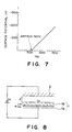
- Figure 7 shows the results of measurements.
- the charging action involves a threshold concerning the DC voltage V DC applied.
- the charging effect starts at approximately 560 V.
- the provided surface potential V by the applied voltage higher than the charge starting voltage is linear with respect to the applied voltage as shown in Figure 7.
- the property is substantially immune to ambient conditions, that is, generally the same results are confirmed under high humidity and high temperature conditions and under low humidity and low temperature conditions.
- Vc Va - V TH
- Vg [(Va-Vc)Z]/(Ls/Ks+Z) (1)
- Figure 10 is a graph showing the results of measurements of the DC voltage applied to the conductive roller 2 and the surface potential of the photosensitive drum 1 after being charged by the conductive roller 2, when the photosensitive layer 1 of the photosensitive drum 1 is replaced by an amorphous silicon photosensitive drum.
- V TH 432 V, which is substantially the same as the results of experiments.
- the inventors applied a vibratory voltage provided by a DC voltage and an AC voltage superposed therewith is applied to the conductive roller. As a result, it has been found that it is effective for elimination of the non-uniformness to superpose to the DC voltage an AC voltage having a certain level of peak-to-peak voltage.
- the OPC photosensitive drum and amorphous silicon photosensitive drum are the same as the ones used in paragraph (1).
- a vibratory voltage (V DC +V AC ) provided by superposing a DC voltage V DC and an AC voltage V AC having a peak-to-peak voltage Vp-p is applied to the conductive roller 2 to contact-charge the amorphous silicon photosensitive drum.
- the peak-to-peak voltage and the charged potential of the surface of the photosensitive drum were measured.
- the potential increases substantially linearly proportionally with Vp-p.
- the potential levels off substantially at the V DC level of the DC component of the applied voltage and becomes substantially constant irrespective of increase of Vp-p.
- the inflection point ⁇ with respect to Vp-p is approx. 1100 V as shown in Figure 3 in the case of OPC photosensitive drum, and approx. 900 V in the case of the amorphous silicon drum as shown in Figure 4. These are approximately twice the charge starting voltage V TH when the DC voltage is applied (paragraph (1)).
- the inflection point ⁇ with respect to Vp-p is constant, although the level-off point of the charged potential changes with the variation of V DC .
- the inflection point is not dependent on the relative speed between the conductive roller 2 and the photosensitive member 1, including for example stopping, forward rotation and backward rotation.
- the surface of the photosensitive drum is charged by the conductive roller supplied by the superposed DC component.
- Vp-p When the level of Vp-p is small, that is, when there is a linear relationship between Vp-p/2 and the charged potential (inclination is 1), a spotty charging results like when a DC voltage alone is applied to the conductive roller 2. However, when the peak-to-peak voltage higher than the inflection point ⁇ is applied, the charged potential level is constant, and the resultant visualized image is uniform, that is, the charging is uniform.
- the inflection point ⁇ is considered to be a starting point where the electric charge starts to transfer back from the photosensitive member to the conductive roller under the vibratory field between the photosensitive member and the conductive roller, provided by the vibratory voltage application.
- FIG. 5 shows a waveform of the voltage applied to the conductive roller.
- the vibratory voltage waveform is a DC component V DC and an AC component Vp-p of a sine wave
- Vmin V DC - Vp-p/2.
- Vc Va - V TH
- V V DC + Vp-p/2 - V TH .
- the charge transfers and transfers back therebetween, wherein the charge transfer is dependent on the threshold V TH . If it is assumed that the charge movement occurs when a potential difference not less than the threshold V TH in a certain determined distance, in the area where the conductive roller and the photosensitive drum are close to each other, the charge potential of the photosensitive drum vibrates in the manner shown in Figure 6 by broken line, which is similar to a pulse wave. As seen from the Figure, the amplitude is Vp-p/2 - T TH .
- the charged potential of the photosensitive drum decreases until the voltage Vmin is applied to the conductive roller.
- the potential of the charged photosensitive drum vibrates with the center of V DC in the pulse-like waveform, as shown in Figure 6 by broken lines.
- the voltage V TH is a potential difference in the smallest distance that produces the charge transfer because of its definition, and therefore, it is dependent on the distance, more particularly, the threshold voltage V TH required for transferring the charge has to be large if the gap between the conductive roller and the photosensitive drum is large.
- the Paschen's curve shown in Figure 9 exhibits increase of the air gap break-down voltage in accordance with increase of the distance.
- the structure is such that the distance between the conductive roller 2 and the photosensitive drum 1 gradually increases toward the downstream from the contact point with respect to movement of the periphery of the photosensitive drum 1, the potential of the charged photosensitive drum having been vibrating in the pulse waveform having an amplitude of Vp-p/2 - V TH as shown in Figure 6 becomes vibrating with smaller amplitude to zero with the increase of the threshold voltage V TH .
- the surface potential of the photosensitive member is not dependent on the peak-to-peak voltage Vp-p of the vibratory voltage applied to the conductive roller, but is stabilized at the level of V DC .
- the shape of the contact member to be contacted to the member to be charged is not inevitably limited to a roller shape.
- the shape may be such that the contact member includes a portion A contacted to the member to be charged and a portion B continuous from the portion A to provide an increasing distance from the member 1 to be charged toward the downstream of the member to be charged with respect to its movement.
- Figures 11A and B show it as a pad contacted to the member to be charged 1.
- the charging device involves the effects similar to those of a grid used with conventional corona dischargers, and therefore, a stabilized charging process is enabled without the phenomena of varied image provided by varied electrostatic latent image in an electrophotographic process.
- the waveform of the vibratory voltage is a sine wave as shown in Figure 5, but this is not limiting, and instead rectangular wave or pulse wave may be usable for the vibratory voltage.
- the charging device according to the present invention is used in an electrophotographic apparatus which is in this example a laser beam printer.
- the photosensitive drum 1 is uniformly charged to a predetermined potential by a conductive roller 2, and thereafter, is scanningly exposed to a laser beam L through a mirror 5, the laser beam L being modulated in accordance with image information from a known laser scanner unit 4. By this exposure, an electrostatic latent image is formed on the photosensitive drum 1 in accordance with the image information. Then, the electrostatic latent image is visualized by the developing device 6.
- the visualized image formed on the photosensitive drum 1 is transferred onto a sheet P by a transfer roller 7 at a transfer station, the sheet P having been transferred by an unshown conveying means.
- the transfer roller 7 is supplied with a DC voltage having a polarity opposite to that of the visualized image from the power source 8.
- the sheet P on which the visualized image is transferred from the transfer roller 7 is conveyed to an image fixing means not shown, where the visualized image is fixed on the sheet P.
- the developer remaining on the photosensitive drum 1 after the image transfer is removed by a cleaner 9, so that the surface of the photosensitive drum 1 is cleaned, and the photosensitive drum is prepared for the next image forming operation.
- the charging device according to the present invention can be employed with the result of good image without non-uniform charging can be provided. This is because of the above-described vibratory voltage applied to the conductive roller 2 from the power source 3.
- the present invention is applicable to the image transfer charging means.
- the scanning exposure means is of a laser beam type, but this is not limiting, and the present invention is applicable to an electrophotographic apparatus having a conventional analog type exposure optical system.
- a vibratory voltage having a peak-to-peak voltage which is not less than twice the absolute value of the charge starting voltage to a member to be charged is applied between the member to be charged and a contacting member contacted thereto to form a vibratory electric field therebetween to charge the member to be charged, whereby spotty charging does not occur on the member to be charged, so that it can be uniformly charged to a predetermined potential always stably.
- a low voltage is usable for charging a member as compared with the voltage necessary in a corona discharging device.
Landscapes
- Physics & Mathematics (AREA)
- Engineering & Computer Science (AREA)
- Plasma & Fusion (AREA)
- General Physics & Mathematics (AREA)
- Electrostatic Charge, Transfer And Separation In Electrography (AREA)
Claims (25)
- Aufladevorrichtung mit:
einem zu ladenden, beweglichen Teil (1);
einem Ladeteil (2), das in einem sich transversal zur Bewegungsrichtung des beweglichen Teils (1) erstreckenden ersten Bereich das bewegliche Teil (1) berührt;
und einer Spannungsquelle (3) zum Zuführen einer Wechselspannung zum Ladeteil,
wobei das Ladeteil und das bewegliche Teil derart geformt sind, daß ein sich in Bewegungsrichtung vergrößernder Spalt gebildet ist,
dadurch gekennzeichnet, daß die Spannungsquelle dem Ladeteil eine Wechselspannung mit einem Spitze-Spitze-Wert von nicht weniger als dem zweifachen einer Schwellspannung (VTH) zuführt, die dem minimalen Gleichspannungswert entspricht, der das bewegliche Teil (1) laden würde, wenn er an das Ladeteil (2) angelegt wäre. - Vorrichtung nach Anspruch 1 in der das Ladeteil an den ersten Bereich angrenzend gewölbt ist.
- Vorrichtung nach Anspruch 1 oder 2, in der das Ladeteil (2) ein Kissen ist.
- Vorrichtung nach Anspruch 1 oder 2, in der das Ladeteil (2) ein drehendes Teil ist.
- Vorrichtung nach Anspruch 4, in der das Ladeteil (2) eine Walze ist.
- Vorrichtung nach einem der vorstehenden Ansprüche, in der die Wechselspannung die Form einer Sinuswelle hat.
- Vorrichtung nach einem der vorstehenden Ansprüche, in der die Spannungsquelle (3) die Wechselspannung durch Überlagern einer Gleichspannung und einer Wechselspannung erzeugt.
- Vorrichtung nach einem der vorstehenden Ansprüche, in der das bewegliche Teil ein photoempfindliches Material enthält.
- Vorrichtung nach Anspruch 8, in der das bewegliche Teil eine Schicht aus einem organischen Photoleiter enthält.
- Vorrichtung nach Anspruch 8, in der das bewegliche Teil eine Schicht aus photoleitendem amorphem Silizium enthält.
- Vorrichtung nach einem der vorstehenden Ansprüche, in der das Ladeteil ein Kernteil (2a) enthält, das von einer inneren Schicht (2b) umhüllt ist, die wiederum von einer äußeren leitenden Schicht (2c) umhüllt ist.
- Vorrichtung nach Anspruch 11, in der die innere Schicht eine elastische Gummischicht und die äußere Schicht eine dispergierten Kohlenstoff enthaltende Urethanschicht ist.
- Vorrichtung nach einem der Ansprüche 1 bis 10, in der das Ladeteil ein Kernteil und eine einzelne umhüllende Schicht aus leitfähigem Material enthält.
- Vorrichtung nach Anspruch 13, in der die umhüllende Schicht eine dispergierten Kohlenstoff enthaltende Urethanschaumschicht ist.
- Vorrichtung nach Anspruch 11, in der die Oberflächenschicht des Ladeteils einen spezifischen Widerstand von 10² bis 10¹⁰ Ohm*cm hat.
- Vorrichtung nach Anspruch 4 oder einem von Anspruch 4 abhängigen Anspruch der Ansprüche 5 bis 15, in der die Oberflächengeschwindigkeit des Ladeteils gleich der des beweglichen Teils ist.
- Vorrichtung nach einem der Ansprüche 11 bis 16, die derart beschaffen ist, daß dann, wenn sich das Ladeteil (2) und ein Teil des beweglichen Teils (1) voneinander entfernen, die elektrische Feldstärke zwischen dem Ladeteil (2) und diesem Teil mit der Zeit ständig geringer wird.
- Verfahren zum Betreiben eines Bilderzeugungsgeräts, das ein zu ladendes Teil (1) und ein das zu ladende Teil (1) berührendes Ladeteil (2) enthält, wobei das Ladeteil (2) einen Bereich enthält, der sich in die selbe Richtung wie das zu ladende Teil (1) erstreckt und einen sich fortschreitend vergrößernden Spalt dazwischen bestimmt, wobei das Verfahren die Schritte des Anlegens einer Wechselspannung zwischen dem Ladeteil (2) und dem zu ladenden Teil (1) und des Bewegens des zu ladenden Teils relativ zum Ladeteil (2) umfaßt, dadurch gekennzeichnet, daß die Spannung einen Spitze-Spitze-Wert hat, der nicht geringer ist als der zweifache Wert einer Schwellspannung (VTH), die dem minimalen Gleichspannungswert entspricht, der das bewegliche Teil (1) laden würde, wenn er an das Ladeteil (2) angelegt wäre.
- Verfahren nach Anspruch 18, bei dem die Spannung eine Wechselspannung mit Gleichspannungsanteil enthält.
- Verfahren nach Anspruch 18 oder 19, bei dem das Ladeteil (2) ein in Kontakt mit dem beweglichen Teil befindliches drehbares Teil enthält.
- Verfahren nach Anspruch 20, bei dem das Ladeteil (2) eine Walze enthält.
- Verfahren nach Anspruch 20 oder 21, bei dem die Oberflächengeschwindigkeit des Ladeteils gleich der des beweglichen Teils ist.
- Verfahren nach Anspruch 18 oder 19, bei dem das Ladeteil (2) ein Kissen aufweist.
- Verfahren nach einem der Ansprüche 18 bis 23, bei dem das Potential, auf das das bewegliche Teil geladen wird, in keinem Zusammenhang zu seinem Potential vor dem Laden steht.
- Verfahren nach einem der Ansprüche 22 bis 24, bei dem die elektrische Feldstärke über dem Spalt zwischen einem geladenen Teilbereich des zu ladenden Teils (1) und dem Ladeteil (2) mit der Zeit ständig geringer wird.
Applications Claiming Priority (4)
| Application Number | Priority Date | Filing Date | Title |
|---|---|---|---|
| JP298419/86 | 1986-12-15 | ||
| JP29841986A JPS63149669A (ja) | 1986-12-15 | 1986-12-15 | 接触帯電方法 |
| JP298420/86 | 1986-12-15 | ||
| JP29842086A JPS63149668A (ja) | 1986-12-15 | 1986-12-15 | 帯電方法及び同装置並びにこの装置を備えた電子写真装置 |
Publications (3)
| Publication Number | Publication Date |
|---|---|
| EP0272072A2 EP0272072A2 (de) | 1988-06-22 |
| EP0272072A3 EP0272072A3 (en) | 1989-03-15 |
| EP0272072B1 true EP0272072B1 (de) | 1994-05-25 |
Family
ID=26561516
Family Applications (1)
| Application Number | Title | Priority Date | Filing Date |
|---|---|---|---|
| EP87310983A Expired - Lifetime EP0272072B1 (de) | 1986-12-15 | 1987-12-14 | Aufladevorrichtung |
Country Status (3)
| Country | Link |
|---|---|
| US (1) | US4851960A (de) |
| EP (1) | EP0272072B1 (de) |
| DE (1) | DE3789893T2 (de) |
Families Citing this family (146)
| Publication number | Priority date | Publication date | Assignee | Title |
|---|---|---|---|---|
| EP0280542B1 (de) * | 1987-02-26 | 1994-11-02 | Canon Kabushiki Kaisha | Bilderzeugungsgerät |
| JPH07113802B2 (ja) * | 1987-06-30 | 1995-12-06 | キヤノン株式会社 | 画像形成装置 |
| DE3885830T2 (de) * | 1987-09-14 | 1994-06-16 | Canon Kk | Aufladevorrichtung. |
| CN1038277C (zh) * | 1987-12-28 | 1998-05-06 | 佳能公司 | 成象设备 |
| JPH0664393B2 (ja) * | 1988-02-11 | 1994-08-22 | キヤノン株式会社 | 帯電用部材、それを有する接触帯電装置、それを用いた接触帯電方法およびそれを有する電子写真装置 |
| JPH0693150B2 (ja) * | 1988-04-20 | 1994-11-16 | キヤノン株式会社 | 画像形成装置 |
| JP2733609B2 (ja) * | 1988-10-29 | 1998-03-30 | キヤノン株式会社 | 転写装置 |
| JP2860404B2 (ja) * | 1989-03-03 | 1999-02-24 | キヤノン株式会社 | 帯電部材および該帯電部材を有する電子写真装置 |
| DE69021234T2 (de) * | 1989-03-14 | 1996-01-04 | Canon Kk | Auflade-Element und elektrofotografisches Gerät mit einem solchen Element. |
| JPH02253288A (ja) * | 1989-03-28 | 1990-10-12 | Canon Inc | 画像形成装置 |
| US5179397A (en) * | 1989-04-03 | 1993-01-12 | Canon Kabushiki Kaisha | Image forming apparatus with constant voltage and constant current control |
| JP2633016B2 (ja) * | 1989-04-05 | 1997-07-23 | キヤノン株式会社 | プロセスカートリッジ及び画像形成装置 |
| EP0400996B1 (de) * | 1989-05-31 | 1994-05-11 | Canon Kabushiki Kaisha | Bilderzeugungsgerät |
| JP2575209B2 (ja) * | 1989-07-05 | 1997-01-22 | キヤノン株式会社 | 電子写真用帯電部材および電子写真装置 |
| KR940010879B1 (ko) * | 1989-07-28 | 1994-11-19 | 캐논 가부시끼가이샤 | 화상형성장치 |
| JPH0387843A (ja) * | 1989-08-31 | 1991-04-12 | Canon Inc | 画像形成装置 |
| JPH0789249B2 (ja) * | 1989-09-14 | 1995-09-27 | キヤノン株式会社 | 画像形成装置 |
| US5095335A (en) * | 1989-09-19 | 1992-03-10 | Canon Kabushiki Kaisha | Copier with retractable charging unit to prevent damage to drum when removing process cartridge |
| JPH03156476A (ja) * | 1989-11-15 | 1991-07-04 | Canon Inc | 画像形成装置の帯電装置 |
| US5177534A (en) * | 1989-12-04 | 1993-01-05 | Canon Kabushiki Kaisha | Image forming apparatus with contact-type charge means |
| US5404198A (en) * | 1989-12-15 | 1995-04-04 | Canon Kabushiki Kaisha | Process cartridge and image forming apparatus |
| US5223893A (en) * | 1989-12-15 | 1993-06-29 | Canon Kabushiki Kaisha | Process cartridge detachably mountable to image forming apparatus |
| US5471284A (en) * | 1990-01-19 | 1995-11-28 | Canon Kabushiki Kaisha | Image forming apparatus having toner depletion detection feature |
| US5623328A (en) * | 1990-04-27 | 1997-04-22 | Canon Kabushiki Kaisha | Process cartridge and image forming system on which process cartridge is mountable |
| EP0453963B1 (de) * | 1990-04-27 | 1997-08-27 | Canon Kabushiki Kaisha | Von einem Bilderzeugungsgerät abnehmbare Arbeitseinheit |
| US5828928A (en) * | 1990-04-27 | 1998-10-27 | Canon Kabushiki Kaisha | Process cartridge mountable in an image forming system and a method for assembling a cleaning device |
| DE69130523T2 (de) * | 1990-09-07 | 1999-05-20 | Konica Corp., Tokio/Tokyo | Aufladevorrichtung |
| EP0476981B1 (de) * | 1990-09-21 | 1995-08-02 | Katsuragawa Electric Co., Ltd. | Verfahren und Gerät zur Erzeugung von elektrophotographischen Bildern |
| US5272505A (en) * | 1990-10-24 | 1993-12-21 | Canon Kabushiki Kaisha | Charging device, process unit having same and image forming apparatus using process unit |
| JP2817391B2 (ja) * | 1990-11-02 | 1998-10-30 | キヤノン株式会社 | 帯電装置 |
| EP0692745B1 (de) | 1990-11-06 | 2000-05-10 | Canon Kabushiki Kaisha | Arbeitseinheit und Bilderzeugungsgerät mit einer solchen Einheit |
| US5294960A (en) * | 1990-11-06 | 1994-03-15 | Canon Kabushiki Kaisha | Detachable two-frame process cartridge for an image forming apparatus |
| US5682579A (en) * | 1990-11-06 | 1997-10-28 | Canon Kabushiki Kaisha | Detachable two-frame process cartridge for an image forming apparatus |
| JP3028617B2 (ja) * | 1991-02-06 | 2000-04-04 | ミノルタ株式会社 | 接触帯電装置 |
| JPH04268583A (ja) * | 1991-02-22 | 1992-09-24 | Canon Inc | 帯電装置 |
| JP2962919B2 (ja) * | 1991-03-01 | 1999-10-12 | キヤノン株式会社 | プロセスカートリッジ及び画像形成装置 |
| JP2899123B2 (ja) * | 1991-03-20 | 1999-06-02 | キヤノン株式会社 | 帯電部材、帯電装置、この帯電装置を備えた画像形成装置及びこの画像形成装置に着脱可能なプロセスユニット |
| JP2561400B2 (ja) * | 1991-07-31 | 1996-12-04 | キヤノン株式会社 | 電子写真装置及びこの装置に着脱可能なプロセスカートリッジ |
| DE69220313T2 (de) * | 1991-09-27 | 1998-01-08 | Bridgestone Corp | Kontaktaufladegerät und Verfahren |
| JP3320756B2 (ja) † | 1991-11-28 | 2002-09-03 | 三菱化学株式会社 | 画像形成方法 |
| JP2574107B2 (ja) * | 1991-12-02 | 1997-01-22 | 株式会社リコー | 帯電ローラ及びその製造方法,及び帯電ローラを用いた画像形成装置及びその帯電装置 |
| DE69325113T2 (de) * | 1992-02-07 | 1999-11-04 | Canon K.K., Tokio/Tokyo | Bilderzeugungsgerät mit einem Auflade-Element in Kontakt mit dem Bildträgerelement |
| EP0562857A2 (de) * | 1992-03-26 | 1993-09-29 | Mita Industrial Co. Ltd. | Elektrifizierungsverfahren und dafür verwendetes Gerät |
| DE69315470T2 (de) * | 1992-04-21 | 1998-07-02 | Sharp Kk | Elektrofotografisches Kopiergerät und Auflademittel dafür |
| JP3339877B2 (ja) * | 1992-05-15 | 2002-10-28 | ミノルタ株式会社 | 接触帯電装置 |
| JPH05333668A (ja) * | 1992-05-29 | 1993-12-17 | Canon Inc | 接触帯電装置、及びプロセスカートリッジ |
| JPH0635302A (ja) * | 1992-07-16 | 1994-02-10 | Canon Inc | 画像形成装置 |
| US5365316A (en) * | 1992-08-20 | 1994-11-15 | Canon Kabushiki Kaisha | Electrophotographic image forming apparatus and its high voltage power source device |
| US5485344A (en) * | 1992-09-28 | 1996-01-16 | Mita Industrial Co., Ltd. | Method of contact-charging the surface of a photosensitive material |
| JPH06138749A (ja) * | 1992-10-30 | 1994-05-20 | Minolta Camera Co Ltd | 接触帯電装置 |
| JPH06161210A (ja) * | 1992-11-20 | 1994-06-07 | Minolta Camera Co Ltd | 接触帯電装置 |
| JP2985594B2 (ja) * | 1992-12-03 | 1999-12-06 | セイコーエプソン株式会社 | 画像形成方法 |
| EP0605242B1 (de) * | 1992-12-26 | 1997-09-03 | Canon Kabushiki Kaisha | Bilderzeugungsvorrichtung mit Aufladeelement, welches mit einer oszillierenden Spannung versorgt wird |
| JP2855042B2 (ja) * | 1993-02-24 | 1999-02-10 | キヤノン株式会社 | カラー画像形成装置 |
| US5966566A (en) * | 1993-03-24 | 1999-10-12 | Canon Kabushiki Kaisha | Recycle method for process cartridge and image forming apparatus |
| JPH06314016A (ja) * | 1993-04-28 | 1994-11-08 | Konica Corp | 帯電装置 |
| JP3011304B2 (ja) * | 1993-05-07 | 2000-02-21 | キヤノン株式会社 | 画像形成装置 |
| US5367364A (en) * | 1993-05-19 | 1994-11-22 | Steven B. Michlin | Charge roller contact stabilizer spring |
| JP2694316B2 (ja) * | 1993-06-17 | 1997-12-24 | シャープ株式会社 | 帯電装置 |
| JPH0728302A (ja) * | 1993-07-07 | 1995-01-31 | Canon Inc | 帯電部材、帯電装置、画像形成装置、及びプロセス カートリッジ |
| EP0642063B1 (de) * | 1993-09-07 | 1999-05-06 | Matsushita Electric Industrial Co., Ltd. | Aufladevorrichtung und Bilderzeugungsgerät mit der Aufladevorrichtung |
| JPH07219312A (ja) * | 1993-12-10 | 1995-08-18 | Canon Inc | 画像形成装置 |
| US5548380A (en) | 1993-12-28 | 1996-08-20 | Matsushita Electric Industrial Co., Ltd. | Charging device and an image forming apparatus using a charging device |
| DE69534979T2 (de) * | 1994-03-16 | 2006-10-26 | Canon K.K. | Aufladeelement und Aufladevorrichtung |
| JPH07271155A (ja) * | 1994-03-26 | 1995-10-20 | Canon Inc | 画像形成装置の制御方法 |
| DE69525996T2 (de) * | 1994-06-22 | 2002-09-19 | Canon K.K., Tokio/Tokyo | Elektrophotographisches Gerät |
| US6548218B1 (en) | 1994-06-22 | 2003-04-15 | Canon Kabushiki Kaisha | Magnetic particles for charging means, and electrophotographic apparatus, process cartridge and image forming method including same |
| TW287263B (de) * | 1994-06-22 | 1996-10-01 | Canon Kk | |
| US5618647A (en) * | 1994-09-02 | 1997-04-08 | Canon Kabushiki Kaisha | Magnetic toner and image forming method |
| EP0729075B1 (de) * | 1995-02-10 | 2001-05-23 | Canon Kabushiki Kaisha | Bildherstellungsverfahren, Bildherstellungsgerät und Tonerelemente |
| US5666606A (en) * | 1995-06-08 | 1997-09-09 | Canon Kabushiki Kaisha | Image forming apparatus comprising contact type charging member |
| EP0751437B1 (de) * | 1995-06-27 | 2001-02-07 | Canon Kabushiki Kaisha | Toner für die Entwicklung elektrostatischer Bilder, Bildherstellungsverfahren, Entwicklungsapparateinheit, und Prozesskassette |
| US5666607A (en) * | 1996-01-11 | 1997-09-09 | Hewlett-Packard Company | Wet contact charging for electrophotography |
| DE69721607T2 (de) * | 1996-02-20 | 2004-03-18 | Canon K.K. | Bildherstellungsverfahren |
| JP3428379B2 (ja) * | 1997-07-11 | 2003-07-22 | シャープ株式会社 | 画像形成装置 |
| US6298205B1 (en) | 1998-09-01 | 2001-10-02 | Canon Kabushiki Kaisha | Charging apparatus which stores electrically conductive particles in granule form |
| JP3315653B2 (ja) * | 1998-09-04 | 2002-08-19 | キヤノン株式会社 | 帯電方法、帯電装置、画像形成装置、及びプロセスカートリッジ |
| JP3376289B2 (ja) | 1998-09-04 | 2003-02-10 | キヤノン株式会社 | 帯電部材、帯電方法、帯電装置、画像形成装置、及びプロセスカートリッジ |
| JP3697090B2 (ja) | 1998-10-26 | 2005-09-21 | キヤノン株式会社 | 電子写真画像形成装置 |
| US6447969B1 (en) | 1999-06-02 | 2002-09-10 | Canon Kabushiki Kaisha | Toner and image forming method |
| US6300024B1 (en) | 1999-06-30 | 2001-10-09 | Canon Kabushiki Kaisha | Toner, two-component type developer, heat fixing method, image forming method and apparatus unit |
| JP3710332B2 (ja) | 1999-07-29 | 2005-10-26 | キヤノン株式会社 | 画像形成装置 |
| JP3703341B2 (ja) | 1999-07-29 | 2005-10-05 | キヤノン株式会社 | 画像形成装置および現像剤・帯電用磁性粒子補給容器 |
| DE60032069T2 (de) | 1999-08-02 | 2007-07-05 | Ricoh Co., Ltd. | Gerät zur Bilderzeugung mit der Möglichkeit zur effektiven Darstellung von einem gleichmässigen Ladungspotential |
| US6337962B1 (en) | 1999-08-12 | 2002-01-08 | Canon Kabushiki Kaisha | Process cartridge and electrophotographic apparatus |
| US6410195B1 (en) | 1999-08-12 | 2002-06-25 | Canon Kabushiki Kaisha | Electrophotographic photosensitive member, process cartridge, and electrophotographic apparatus |
| EP1089132B1 (de) | 1999-09-30 | 2008-10-08 | Canon Kabushiki Kaisha | Herstellungsverfahren für ein leitendes Bauteil für einen Bilderzeugungsgerät |
| JP2001109230A (ja) | 1999-10-08 | 2001-04-20 | Canon Inc | 画像形成装置 |
| US6532347B2 (en) | 2000-01-20 | 2003-03-11 | Canon Kabushiki Kaisha | Method of controlling an AC voltage applied to an electrifier |
| DE60111436T2 (de) * | 2000-02-21 | 2006-05-11 | Canon K.K. | Entwickler, Bildherstellungsverfahren und Prozesskartusche |
| JP4298114B2 (ja) * | 2000-02-21 | 2009-07-15 | キヤノン株式会社 | 現像剤並びに該現像剤を用いた画像形成方法及びプロセスカートリッジ |
| DE60115737T2 (de) | 2000-02-21 | 2006-07-27 | Canon K.K. | Magnetischer Toner und Bildherstellungsverfahren unter Verwendung desselben |
| JP3780171B2 (ja) | 2000-03-03 | 2006-05-31 | キヤノン株式会社 | プロセスカートリッジ、及び、電子写真画像形成装置 |
| CA2337087C (en) | 2000-03-08 | 2006-06-06 | Canon Kabushiki Kaisha | Magnetic toner, process for production thereof, and image forming method, apparatus and process cartridge using the toner |
| JP3283500B2 (ja) | 2000-06-28 | 2002-05-20 | キヤノン株式会社 | プロセスカートリッジの再生産方法 |
| JP3283501B2 (ja) | 2000-06-28 | 2002-05-20 | キヤノン株式会社 | プロセスカートリッジの再生産方法 |
| US6470162B2 (en) | 2000-08-02 | 2002-10-22 | Canon Kabushiki Kaisha | Conductive member, process cartridge and electrophotographic apparatus |
| US20020041365A1 (en) | 2000-09-22 | 2002-04-11 | Takao Sameshima | Image forming apparatus and image forming unit detachably mountable thereto |
| EP1193559B1 (de) | 2000-09-29 | 2008-10-29 | Canon Kabushiki Kaisha | Elektrophotographisches, lichtempfindliches Element, Prozesskartusche und elektrophotographischer Apparat |
| DE60126461T2 (de) | 2000-11-15 | 2007-10-25 | Canon K.K. | Bilderzeugungsverfahren und Bilderzeugungsvorrichtung |
| JP3513488B2 (ja) | 2000-12-20 | 2004-03-31 | キヤノン株式会社 | プロセスカートリッジの再生産方法 |
| JP2002214983A (ja) | 2001-01-15 | 2002-07-31 | Canon Inc | 画像形成装置及びその像担持体寿命検知方法、並びに画像形成装置に着脱可能なカートリッジ |
| JP2002296875A (ja) | 2001-03-29 | 2002-10-09 | Canon Inc | 帯電ローラ、帯電装置、画像形成装置及びプロセスカートリッジ |
| JP3848097B2 (ja) * | 2001-04-20 | 2006-11-22 | キヤノン株式会社 | 帯電部材、帯電装置、画像形成装置及びプロセスカートリッジ |
| US6697591B2 (en) | 2001-06-21 | 2004-02-24 | Canon Kabushiki Kaisha | Electrophotographic apparatus and process cartridge |
| JP3997065B2 (ja) | 2001-08-20 | 2007-10-24 | キヤノン株式会社 | プロセスカートリッジ及び画像形成装置 |
| JP2003228237A (ja) | 2002-02-01 | 2003-08-15 | Canon Inc | 画像形成装置 |
| CN1259600C (zh) | 2002-02-21 | 2006-06-14 | 佳能化成株式会社 | 带电辊、成像处理盒和电子照相装置 |
| JP3903021B2 (ja) * | 2002-04-09 | 2007-04-11 | キヤノン株式会社 | 画像形成装置および画像形成制御システム |
| US6882806B2 (en) * | 2002-04-09 | 2005-04-19 | Canon Kabushiki Kaisha | Charging apparatus determining a peak-to-peak voltage to be applied to a charging member |
| JP4065496B2 (ja) * | 2002-04-19 | 2008-03-26 | キヤノン株式会社 | 画像形成装置 |
| JP4194298B2 (ja) | 2002-05-17 | 2008-12-10 | キヤノン株式会社 | 情報記憶媒体、ユニット、プロセスカートリッジ、現像カートリッジおよび電子写真画像形成装置 |
| JP2004021127A (ja) * | 2002-06-19 | 2004-01-22 | Canon Inc | 磁性トナー、該トナーを用いた画像形成方法及びプロセスカートリッジ |
| JP4208513B2 (ja) * | 2002-07-25 | 2009-01-14 | キヤノン株式会社 | 画像形成装置 |
| JP3919641B2 (ja) * | 2002-09-24 | 2007-05-30 | キヤノン株式会社 | 画像形成装置 |
| JP4272866B2 (ja) * | 2002-09-27 | 2009-06-03 | キヤノン株式会社 | 画像形成装置 |
| EP2244129B1 (de) * | 2002-10-02 | 2012-07-18 | Canon Kabushiki Kaisha | Feine Silica-Partikel, Toner, Zweikomponentenentwickler und Bilderzeugungsverfahren |
| JP3793192B2 (ja) * | 2002-10-25 | 2006-07-05 | キヤノン株式会社 | 画像形成装置 |
| US6763207B2 (en) * | 2002-12-13 | 2004-07-13 | Xerox Corporation | Intermittent DC bias charge roll with DC offset voltage |
| US6807389B2 (en) * | 2002-12-13 | 2004-10-19 | Xerox Corporation | Bias charge roller with optimally induced AC corona |
| US6842594B2 (en) * | 2002-12-13 | 2005-01-11 | Xerox Corporation | Intermittent DC bias charge roll AC cleaning cycle |
| KR100676790B1 (ko) * | 2003-02-07 | 2007-02-02 | 샤프 가부시키가이샤 | 전자 사진 감광체 및 그것을 구비하는 화상 형성 장치 |
| US7162173B2 (en) * | 2003-02-27 | 2007-01-09 | Canon Kabushiki Kaisha | Image forming apparatus using an ordered set of first, second and charging AC peak to peak voltages |
| US7171141B2 (en) * | 2003-04-07 | 2007-01-30 | Canon Kasei Kabushiki Kaisha | Charging roller, process cartridge and electrophotographic apparatus |
| JP3718508B2 (ja) * | 2003-06-03 | 2005-11-24 | シャープ株式会社 | 電子写真感光体およびそれを備える画像形成装置 |
| JP3958272B2 (ja) * | 2003-09-25 | 2007-08-15 | キヤノン株式会社 | プロセスカートリッジ及び電子写真画像形成装置 |
| US7139501B2 (en) * | 2003-11-20 | 2006-11-21 | Canon Kabushiki Kaisha | Charge voltage control circuit and image forming apparatus which controls a charge voltage based on a discharge current |
| US7177572B2 (en) * | 2004-06-25 | 2007-02-13 | Xerox Corporation | Biased charge roller with embedded electrodes with post-nip breakdown to enable improved charge uniformity |
| US7280779B2 (en) * | 2004-12-26 | 2007-10-09 | Hewlett-Packard Development Company, L.P. | Image banding compensation method |
| JP4330082B2 (ja) * | 2007-03-06 | 2009-09-09 | 京セラミタ株式会社 | 画像形成装置 |
| US7899352B2 (en) * | 2007-03-06 | 2011-03-01 | Kyocera Mita Corporation | Image forming apparatus |
| JP2009103830A (ja) * | 2007-10-22 | 2009-05-14 | Kyocera Mita Corp | 画像形成装置 |
| JP5219452B2 (ja) * | 2007-10-22 | 2013-06-26 | 京セラドキュメントソリューションズ株式会社 | 画像形成装置 |
| JP2009300821A (ja) * | 2008-06-16 | 2009-12-24 | Konica Minolta Business Technologies Inc | 画像形成ユニットおよび画像形成装置 |
| JP5455336B2 (ja) * | 2008-08-19 | 2014-03-26 | キヤノン株式会社 | 帯電部材、帯電装置、画像形成装置、及びプロセスカートリッジ |
| JP5308838B2 (ja) * | 2009-01-19 | 2013-10-09 | 京セラドキュメントソリューションズ株式会社 | 画像形成装置 |
| JP5473501B2 (ja) * | 2009-09-08 | 2014-04-16 | キヤノン株式会社 | 画像形成装置 |
| US8320817B2 (en) | 2010-08-18 | 2012-11-27 | Eastman Kodak Company | Charge removal from a sheet |
| US9170518B2 (en) | 2010-08-26 | 2015-10-27 | Xerox Corporation | Method and system for closed-loop control of nip width and image transfer field uniformity for an image transfer system |
| US8396404B2 (en) | 2010-08-26 | 2013-03-12 | Xerox Corporation | Image transfer nip method and apparatus using constant current controls |
| US20120099911A1 (en) | 2010-10-21 | 2012-04-26 | Mark Cameron Zaretsky | Concurrently removing sheet charge and curl |
| US9014585B2 (en) | 2013-03-15 | 2015-04-21 | Xerox Corporation | System and method for detecting bias transfer roll positions using resistance detection |
| CN104076637B (zh) * | 2013-03-26 | 2016-06-22 | 京瓷办公信息系统株式会社 | 图像形成装置 |
| CN113306413B (zh) * | 2016-08-31 | 2022-07-26 | 袁博 | 一种适用于锂电池的具有通讯功能的直流充电器 |
| JP6589889B2 (ja) | 2017-01-06 | 2019-10-16 | 京セラドキュメントソリューションズ株式会社 | 画像形成装置 |
| JP7475228B2 (ja) | 2020-07-17 | 2024-04-26 | シャープ株式会社 | 画像形成装置 |
Family Cites Families (7)
| Publication number | Priority date | Publication date | Assignee | Title |
|---|---|---|---|---|
| JPS56104347A (en) * | 1980-01-23 | 1981-08-20 | Toshiba Corp | Charging device of electrophotographic copier |
| DE3101678C2 (de) * | 1980-01-25 | 1983-07-07 | Tokyo Shibaura Denki K.K., Kawasaki, Kanagawa | Einrichtung zum gleichförmigen Aufladen eines kontinuierlich durch eine Aufladezone bewegten elektrofotografischen Aufzeichnungsmaterials |
| DE3164262D1 (en) * | 1980-03-10 | 1984-07-26 | Tokyo Shibaura Electric Co | Charging device |
| JPS5767951A (en) * | 1980-10-14 | 1982-04-24 | Toshiba Corp | Electric charger |
| CA1214502A (en) * | 1982-11-01 | 1986-11-25 | Lloyd F. Bean | Cleaning method and apparatus for a xerographic reproducing apparatus |
| JPS60216361A (ja) * | 1984-04-12 | 1985-10-29 | Fuji Xerox Co Ltd | ブラシ帯電・転写装置 |
| EP0280542B1 (de) * | 1987-02-26 | 1994-11-02 | Canon Kabushiki Kaisha | Bilderzeugungsgerät |
-
1987
- 1987-12-11 US US07/131,585 patent/US4851960A/en not_active Ceased
- 1987-12-14 DE DE3789893T patent/DE3789893T2/de not_active Expired - Lifetime
- 1987-12-14 EP EP87310983A patent/EP0272072B1/de not_active Expired - Lifetime
Also Published As
| Publication number | Publication date |
|---|---|
| US4851960A (en) | 1989-07-25 |
| DE3789893D1 (de) | 1994-06-30 |
| EP0272072A2 (de) | 1988-06-22 |
| DE3789893T2 (de) | 1994-09-15 |
| EP0272072A3 (en) | 1989-03-15 |
Similar Documents
| Publication | Publication Date | Title |
|---|---|---|
| EP0272072B1 (de) | Aufladevorrichtung | |
| EP0280542B1 (de) | Bilderzeugungsgerät | |
| US5534344A (en) | Charging member having a loosely supported charger portion | |
| JPH0352058B2 (de) | ||
| USRE35581E (en) | Charging device | |
| EP0747780A2 (de) | Bilderzeugungsgerät mit Kontaktaufladungsteil | |
| US5621506A (en) | Electrostatic recording apparatus providing an electric field adjacent a developer roller | |
| US6622000B2 (en) | Developing apparatus having a charge amount control member | |
| EP0642063B1 (de) | Aufladevorrichtung und Bilderzeugungsgerät mit der Aufladevorrichtung | |
| US5539505A (en) | Commutating method for SCD donor roll bias | |
| US5543900A (en) | Image forming apparatus which reduces toner fusion on an image bearing member | |
| JP2919205B2 (ja) | 帯電方法 | |
| EP0496399A2 (de) | Aufladevorrichtung zum Aufladen eines sich in der Nähe befindendes Elementes und Bilderzeugungsgerät mit einer solchen Vorrichtung | |
| JPH05150564A (ja) | 接触帯電方法及びその装置 | |
| JPH04240671A (ja) | 帯電装置及びこれを備えた画像形成装置 | |
| JP3715552B2 (ja) | 現像装置およびこれを備えた画像形成装置 | |
| JPH05303259A (ja) | 接触帯電装置 | |
| JP2020122848A (ja) | 画像形成装置 | |
| JP3356185B2 (ja) | 画像形成装置 | |
| JPH04218076A (ja) | 接触帯電方法 | |
| JPH1172977A (ja) | 画像形成装置 | |
| JP2887025B2 (ja) | 画像形成方法における帯電方法 | |
| JPH11219003A (ja) | 帯電装置 | |
| US20050089346A1 (en) | Spaced biased roll charging member having clipped AC input voltage | |
| JPH04245265A (ja) | 帯電装置及びこれを備えた画像形成装置 |
Legal Events
| Date | Code | Title | Description |
|---|---|---|---|
| PUAI | Public reference made under article 153(3) epc to a published international application that has entered the european phase |
Free format text: ORIGINAL CODE: 0009012 |
|
| AK | Designated contracting states |
Kind code of ref document: A2 Designated state(s): DE FR GB IT |
|
| PUAL | Search report despatched |
Free format text: ORIGINAL CODE: 0009013 |
|
| AK | Designated contracting states |
Kind code of ref document: A3 Designated state(s): DE FR GB IT |
|
| 17P | Request for examination filed |
Effective date: 19890809 |
|
| 17Q | First examination report despatched |
Effective date: 19910708 |
|
| GRAA | (expected) grant |
Free format text: ORIGINAL CODE: 0009210 |
|
| AK | Designated contracting states |
Kind code of ref document: B1 Designated state(s): DE FR GB IT |
|
| REF | Corresponds to: |
Ref document number: 3789893 Country of ref document: DE Date of ref document: 19940630 |
|
| ET | Fr: translation filed | ||
| ITF | It: translation for a ep patent filed | ||
| ITTA | It: last paid annual fee | ||
| PLBE | No opposition filed within time limit |
Free format text: ORIGINAL CODE: 0009261 |
|
| STAA | Information on the status of an ep patent application or granted ep patent |
Free format text: STATUS: NO OPPOSITION FILED WITHIN TIME LIMIT |
|
| 26N | No opposition filed | ||
| REG | Reference to a national code |
Ref country code: GB Ref legal event code: IF02 |
|
| PGFP | Annual fee paid to national office [announced via postgrant information from national office to epo] |
Ref country code: GB Payment date: 20061218 Year of fee payment: 20 |
|
| PGFP | Annual fee paid to national office [announced via postgrant information from national office to epo] |
Ref country code: IT Payment date: 20061231 Year of fee payment: 20 |
|
| PGFP | Annual fee paid to national office [announced via postgrant information from national office to epo] |
Ref country code: DE Payment date: 20070219 Year of fee payment: 20 |
|
| REG | Reference to a national code |
Ref country code: GB Ref legal event code: PE20 |
|
| PG25 | Lapsed in a contracting state [announced via postgrant information from national office to epo] |
Ref country code: GB Free format text: LAPSE BECAUSE OF EXPIRATION OF PROTECTION Effective date: 20071213 |
|
| PGFP | Annual fee paid to national office [announced via postgrant information from national office to epo] |
Ref country code: FR Payment date: 20061218 Year of fee payment: 20 |