WO2016174997A1 - エピタキシャルシリコンウェーハの製造方法 - Google Patents
エピタキシャルシリコンウェーハの製造方法 Download PDFInfo
- Publication number
- WO2016174997A1 WO2016174997A1 PCT/JP2016/061088 JP2016061088W WO2016174997A1 WO 2016174997 A1 WO2016174997 A1 WO 2016174997A1 JP 2016061088 W JP2016061088 W JP 2016061088W WO 2016174997 A1 WO2016174997 A1 WO 2016174997A1
- Authority
- WO
- WIPO (PCT)
- Prior art keywords
- silicon wafer
- epitaxial
- hydrogen
- epitaxial film
- oxide film
- Prior art date
- Legal status (The legal status is an assumption and is not a legal conclusion. Google has not performed a legal analysis and makes no representation as to the accuracy of the status listed.)
- Ceased
Links
Images


Classifications
-
- C—CHEMISTRY; METALLURGY
- C30—CRYSTAL GROWTH
- C30B—SINGLE-CRYSTAL GROWTH; UNIDIRECTIONAL SOLIDIFICATION OF EUTECTIC MATERIAL OR UNIDIRECTIONAL DEMIXING OF EUTECTOID MATERIAL; REFINING BY ZONE-MELTING OF MATERIAL; PRODUCTION OF A HOMOGENEOUS POLYCRYSTALLINE MATERIAL WITH DEFINED STRUCTURE; SINGLE CRYSTALS OR HOMOGENEOUS POLYCRYSTALLINE MATERIAL WITH DEFINED STRUCTURE; AFTER-TREATMENT OF SINGLE CRYSTALS OR A HOMOGENEOUS POLYCRYSTALLINE MATERIAL WITH DEFINED STRUCTURE; APPARATUS THEREFOR
- C30B25/00—Single-crystal growth by chemical reaction of reactive gases, e.g. chemical vapour-deposition growth
- C30B25/02—Epitaxial-layer growth
- C30B25/18—Epitaxial-layer growth characterised by the substrate
- C30B25/186—Epitaxial-layer growth characterised by the substrate being specially pre-treated by, e.g. chemical or physical means
-
- H—ELECTRICITY
- H10—SEMICONDUCTOR DEVICES; ELECTRIC SOLID-STATE DEVICES NOT OTHERWISE PROVIDED FOR
- H10P—GENERIC PROCESSES OR APPARATUS FOR THE MANUFACTURE OR TREATMENT OF DEVICES COVERED BY CLASS H10
- H10P14/00—Formation of materials, e.g. in the shape of layers or pillars
- H10P14/60—Formation of materials, e.g. in the shape of layers or pillars of insulating materials
- H10P14/63—Formation of materials, e.g. in the shape of layers or pillars of insulating materials characterised by the formation processes
- H10P14/6326—Deposition processes
- H10P14/6349—Deposition of epitaxial materials
-
- C—CHEMISTRY; METALLURGY
- C30—CRYSTAL GROWTH
- C30B—SINGLE-CRYSTAL GROWTH; UNIDIRECTIONAL SOLIDIFICATION OF EUTECTIC MATERIAL OR UNIDIRECTIONAL DEMIXING OF EUTECTOID MATERIAL; REFINING BY ZONE-MELTING OF MATERIAL; PRODUCTION OF A HOMOGENEOUS POLYCRYSTALLINE MATERIAL WITH DEFINED STRUCTURE; SINGLE CRYSTALS OR HOMOGENEOUS POLYCRYSTALLINE MATERIAL WITH DEFINED STRUCTURE; AFTER-TREATMENT OF SINGLE CRYSTALS OR A HOMOGENEOUS POLYCRYSTALLINE MATERIAL WITH DEFINED STRUCTURE; APPARATUS THEREFOR
- C30B25/00—Single-crystal growth by chemical reaction of reactive gases, e.g. chemical vapour-deposition growth
- C30B25/02—Epitaxial-layer growth
- C30B25/18—Epitaxial-layer growth characterised by the substrate
- C30B25/20—Epitaxial-layer growth characterised by the substrate the substrate being of the same materials as the epitaxial layer
-
- C—CHEMISTRY; METALLURGY
- C30—CRYSTAL GROWTH
- C30B—SINGLE-CRYSTAL GROWTH; UNIDIRECTIONAL SOLIDIFICATION OF EUTECTIC MATERIAL OR UNIDIRECTIONAL DEMIXING OF EUTECTOID MATERIAL; REFINING BY ZONE-MELTING OF MATERIAL; PRODUCTION OF A HOMOGENEOUS POLYCRYSTALLINE MATERIAL WITH DEFINED STRUCTURE; SINGLE CRYSTALS OR HOMOGENEOUS POLYCRYSTALLINE MATERIAL WITH DEFINED STRUCTURE; AFTER-TREATMENT OF SINGLE CRYSTALS OR A HOMOGENEOUS POLYCRYSTALLINE MATERIAL WITH DEFINED STRUCTURE; APPARATUS THEREFOR
- C30B29/00—Single crystals or homogeneous polycrystalline material with defined structure characterised by the material or by their shape
- C30B29/02—Elements
- C30B29/06—Silicon
-
- C—CHEMISTRY; METALLURGY
- C30—CRYSTAL GROWTH
- C30B—SINGLE-CRYSTAL GROWTH; UNIDIRECTIONAL SOLIDIFICATION OF EUTECTIC MATERIAL OR UNIDIRECTIONAL DEMIXING OF EUTECTOID MATERIAL; REFINING BY ZONE-MELTING OF MATERIAL; PRODUCTION OF A HOMOGENEOUS POLYCRYSTALLINE MATERIAL WITH DEFINED STRUCTURE; SINGLE CRYSTALS OR HOMOGENEOUS POLYCRYSTALLINE MATERIAL WITH DEFINED STRUCTURE; AFTER-TREATMENT OF SINGLE CRYSTALS OR A HOMOGENEOUS POLYCRYSTALLINE MATERIAL WITH DEFINED STRUCTURE; APPARATUS THEREFOR
- C30B33/00—After-treatment of single crystals or homogeneous polycrystalline material with defined structure
- C30B33/02—Heat treatment
-
- C—CHEMISTRY; METALLURGY
- C30—CRYSTAL GROWTH
- C30B—SINGLE-CRYSTAL GROWTH; UNIDIRECTIONAL SOLIDIFICATION OF EUTECTIC MATERIAL OR UNIDIRECTIONAL DEMIXING OF EUTECTOID MATERIAL; REFINING BY ZONE-MELTING OF MATERIAL; PRODUCTION OF A HOMOGENEOUS POLYCRYSTALLINE MATERIAL WITH DEFINED STRUCTURE; SINGLE CRYSTALS OR HOMOGENEOUS POLYCRYSTALLINE MATERIAL WITH DEFINED STRUCTURE; AFTER-TREATMENT OF SINGLE CRYSTALS OR A HOMOGENEOUS POLYCRYSTALLINE MATERIAL WITH DEFINED STRUCTURE; APPARATUS THEREFOR
- C30B33/00—After-treatment of single crystals or homogeneous polycrystalline material with defined structure
- C30B33/08—Etching
- C30B33/12—Etching in gas atmosphere or plasma
-
- H—ELECTRICITY
- H10—SEMICONDUCTOR DEVICES; ELECTRIC SOLID-STATE DEVICES NOT OTHERWISE PROVIDED FOR
- H10P—GENERIC PROCESSES OR APPARATUS FOR THE MANUFACTURE OR TREATMENT OF DEVICES COVERED BY CLASS H10
- H10P14/00—Formation of materials, e.g. in the shape of layers or pillars
- H10P14/20—Formation of materials, e.g. in the shape of layers or pillars of semiconductor materials
- H10P14/24—Formation of materials, e.g. in the shape of layers or pillars of semiconductor materials using chemical vapour deposition [CVD]
-
- H—ELECTRICITY
- H10—SEMICONDUCTOR DEVICES; ELECTRIC SOLID-STATE DEVICES NOT OTHERWISE PROVIDED FOR
- H10P—GENERIC PROCESSES OR APPARATUS FOR THE MANUFACTURE OR TREATMENT OF DEVICES COVERED BY CLASS H10
- H10P14/00—Formation of materials, e.g. in the shape of layers or pillars
- H10P14/20—Formation of materials, e.g. in the shape of layers or pillars of semiconductor materials
- H10P14/29—Formation of materials, e.g. in the shape of layers or pillars of semiconductor materials characterised by the substrates
- H10P14/2901—Materials
- H10P14/2902—Materials being Group IVA materials
- H10P14/2905—Silicon, silicon germanium or germanium
-
- H—ELECTRICITY
- H10—SEMICONDUCTOR DEVICES; ELECTRIC SOLID-STATE DEVICES NOT OTHERWISE PROVIDED FOR
- H10P—GENERIC PROCESSES OR APPARATUS FOR THE MANUFACTURE OR TREATMENT OF DEVICES COVERED BY CLASS H10
- H10P14/00—Formation of materials, e.g. in the shape of layers or pillars
- H10P14/20—Formation of materials, e.g. in the shape of layers or pillars of semiconductor materials
- H10P14/34—Deposited materials, e.g. layers
- H10P14/3402—Deposited materials, e.g. layers characterised by the chemical composition
- H10P14/3404—Deposited materials, e.g. layers characterised by the chemical composition being Group IVA materials
- H10P14/3411—Silicon, silicon germanium or germanium
-
- H—ELECTRICITY
- H10—SEMICONDUCTOR DEVICES; ELECTRIC SOLID-STATE DEVICES NOT OTHERWISE PROVIDED FOR
- H10P—GENERIC PROCESSES OR APPARATUS FOR THE MANUFACTURE OR TREATMENT OF DEVICES COVERED BY CLASS H10
- H10P14/00—Formation of materials, e.g. in the shape of layers or pillars
- H10P14/20—Formation of materials, e.g. in the shape of layers or pillars of semiconductor materials
- H10P14/34—Deposited materials, e.g. layers
- H10P14/3402—Deposited materials, e.g. layers characterised by the chemical composition
- H10P14/3424—Deposited materials, e.g. layers characterised by the chemical composition being Group IIB-VIA materials
- H10P14/3426—Oxides
-
- H—ELECTRICITY
- H10—SEMICONDUCTOR DEVICES; ELECTRIC SOLID-STATE DEVICES NOT OTHERWISE PROVIDED FOR
- H10P—GENERIC PROCESSES OR APPARATUS FOR THE MANUFACTURE OR TREATMENT OF DEVICES COVERED BY CLASS H10
- H10P14/00—Formation of materials, e.g. in the shape of layers or pillars
- H10P14/20—Formation of materials, e.g. in the shape of layers or pillars of semiconductor materials
- H10P14/34—Deposited materials, e.g. layers
- H10P14/3438—Doping during depositing
- H10P14/3441—Conductivity type
- H10P14/3442—N-type
-
- H—ELECTRICITY
- H10—SEMICONDUCTOR DEVICES; ELECTRIC SOLID-STATE DEVICES NOT OTHERWISE PROVIDED FOR
- H10P—GENERIC PROCESSES OR APPARATUS FOR THE MANUFACTURE OR TREATMENT OF DEVICES COVERED BY CLASS H10
- H10P14/00—Formation of materials, e.g. in the shape of layers or pillars
- H10P14/20—Formation of materials, e.g. in the shape of layers or pillars of semiconductor materials
- H10P14/34—Deposited materials, e.g. layers
- H10P14/3451—Structure
- H10P14/3452—Microstructure
- H10P14/3458—Monocrystalline
-
- H—ELECTRICITY
- H10—SEMICONDUCTOR DEVICES; ELECTRIC SOLID-STATE DEVICES NOT OTHERWISE PROVIDED FOR
- H10P—GENERIC PROCESSES OR APPARATUS FOR THE MANUFACTURE OR TREATMENT OF DEVICES COVERED BY CLASS H10
- H10P14/00—Formation of materials, e.g. in the shape of layers or pillars
- H10P14/20—Formation of materials, e.g. in the shape of layers or pillars of semiconductor materials
- H10P14/36—Formation of materials, e.g. in the shape of layers or pillars of semiconductor materials characterised by treatments done before the formation of the materials
-
- H—ELECTRICITY
- H10—SEMICONDUCTOR DEVICES; ELECTRIC SOLID-STATE DEVICES NOT OTHERWISE PROVIDED FOR
- H10P—GENERIC PROCESSES OR APPARATUS FOR THE MANUFACTURE OR TREATMENT OF DEVICES COVERED BY CLASS H10
- H10P90/00—Preparation of wafers not covered by a single main group of this subclass, e.g. wafer reinforcement
-
- H—ELECTRICITY
- H10—SEMICONDUCTOR DEVICES; ELECTRIC SOLID-STATE DEVICES NOT OTHERWISE PROVIDED FOR
- H10P—GENERIC PROCESSES OR APPARATUS FOR THE MANUFACTURE OR TREATMENT OF DEVICES COVERED BY CLASS H10
- H10P90/00—Preparation of wafers not covered by a single main group of this subclass, e.g. wafer reinforcement
- H10P90/12—Preparing bulk and homogeneous wafers
- H10P90/126—Preparing bulk and homogeneous wafers by chemical etching
-
- H—ELECTRICITY
- H10—SEMICONDUCTOR DEVICES; ELECTRIC SOLID-STATE DEVICES NOT OTHERWISE PROVIDED FOR
- H10P—GENERIC PROCESSES OR APPARATUS FOR THE MANUFACTURE OR TREATMENT OF DEVICES COVERED BY CLASS H10
- H10P95/00—Generic processes or apparatus for manufacture or treatments not covered by the other groups of this subclass
- H10P95/90—Thermal treatments, e.g. annealing or sintering
Definitions
- the present invention relates to a method for manufacturing an epitaxial silicon wafer.
- an epitaxial silicon wafer for power MOS transistors is required to have a very low substrate resistivity.
- a silicon wafer resists molten silicon in the pulling process of a single crystal ingot (hereinafter referred to as a single crystal ingot) that is a material of the silicon wafer (that is, when growing a silicon crystal).
- a technique of doping arsenic (As) or antimony (Sb) as an n-type dopant for adjusting the rate is known.
- arsenic (As) or antimony (Sb) as an n-type dopant for adjusting the rate.
- these dopants are very easy to evaporate, it is difficult to make the dopant concentration in the silicon crystal sufficiently high, and it is difficult to manufacture a silicon wafer having a resistivity as low as required.
- a silicon wafer having a very low substrate resistivity doped with phosphorus (P) at a high concentration is being used as an n-type dopant having relatively low volatility than arsenic (As) and antimony (Sb) (for example, see Patent Documents 1 and 2).
- Patent Documents 1 and 2 when an epitaxial film is grown on a silicon wafer doped with high-concentration phosphorus, a number of stacking faults (stacking faults, hereinafter referred to as SF) occur in the epitaxial film, and the SF is formed as a step. It is described that it appears on the surface of the wafer, and the LPD (Light Point Defect) level of the surface of the silicon wafer is greatly deteriorated. The cause of this SF is inferred as follows.
- the manufacturing method of Patent Document 1 paying attention to the correlation between the solidification rate of the single crystal ingot, the thermal history, and the generation of SF, the time during which the temperature of the single crystal ingot at the time of pulling is within the range of 570 ° C. ⁇ 70 ° C. is set. By controlling, generation
- argon annealing treatment an argon gas atmosphere
- An object of the present invention is to provide an epitaxial silicon wafer manufacturing method capable of sufficiently suppressing the generation of SF with a simple configuration even when a silicon wafer having an extremely low resistivity is used.
- Patent Document 1 As a result of intensive studies, the present inventor has found the following knowledge. First, as described in Patent Document 1, it is already known that there is a correlation between the solidification rate of single crystal ingot, thermal history, and SF generation. An experiment was conducted to examine the effect of resistivity on the correlation.
- a shoulder is formed with a shoulder that is continuous with the seed crystal and gradually increases in diameter (shoulder forming step), and a straight body that is formed continuously with the shoulder and has a substantially uniform diameter. Forming a portion (straight body portion forming step) and a step (tail portion forming step) of forming a tail portion that is continuous with the lower end of the straight body portion and whose diameter gradually decreases to zero.
- the process (cooling process) which cools a single crystal ingot is performed, and a single crystal ingot is taken out from a pulling apparatus. Due to such manufacturing conditions, it is considered that the time after exiting from the dopant-added melt becomes shorter as it approaches the lower end (bottom) of the single crystal ingot, that is, as the solidification rate increases.
- the solidification rate is the ratio of the pulling weight of the single crystal ingot to the initial charge weight of the dopant-added melt initially stored in the quartz crucible.
- the number of SFs is substantially correlated with the residence time of the single crystal ingot at 570 ° C. ⁇ 70 ° C., and may be 0 at a portion where the solidification rate is greater than 70%. I understood.
- the number of SFs is substantially correlated with the residence time of the single crystal ingot at 570 ° C. ⁇ 70 ° C. in the portion where the solidification rate is 75% or less, but in the portion where the solidification rate is greater than 75%. It was found that there was no correlation with the staying time, and the SF increased toward the bottom.
- the substrate resistivity at the position where the solidification rate was 75% was about 0.7 m ⁇ ⁇ cm.
- a single crystal ingot produced under the same conditions as in Experimental Example 2 was prepared.
- a plurality of silicon wafers were cut out from an intermediate region with the largest SF in the single crystal ingot and a bottom region in which the SF increased toward the bottom.
- the substrate resistivity in the intermediate region was greater than 0.7 m ⁇ ⁇ cm and 0.9 m ⁇ ⁇ cm or less, and the substrate resistivity in the bottom region was 0.7 m ⁇ ⁇ cm or less.
- the intermediate region is a region having a solidification rate of 50% to 60% in FIG. 2
- the bottom region is a region having a solidification rate of 75% or more in FIG.
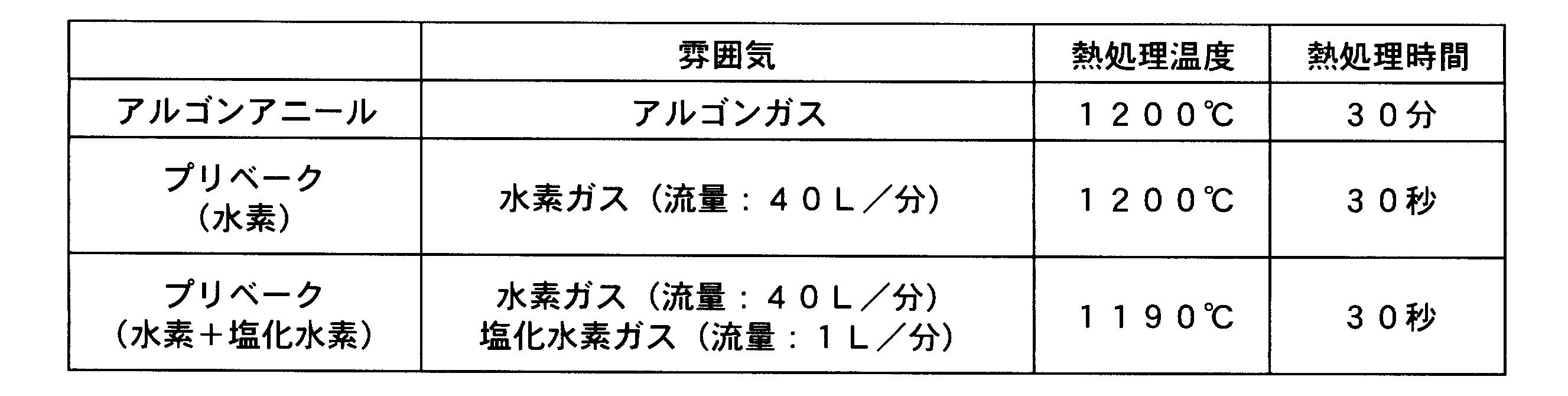
- the silicon wafers obtained from the intermediate region and the bottom region were subjected to the processes shown in Tables 2 and 3 below to produce epitaxial silicon wafers of Experimental Examples 3 to 8, and the number of SFs was evaluated. .
- the results of Experimental Examples 3 to 5 are shown in FIG. 3, and the results of Experimental Examples 6 to 8 are shown in FIG.
- the epitaxial film was grown under the same conditions as in Experimental Examples 1 and 2. Also, argon annealing or prebaking was performed without providing a polysilicon film on the back surface of the silicon wafer.
- the SF in the bottom region is smaller than that in the intermediate region.
- the number of SFs is 0.1 / cm 2 or more and 1.0 / cm 2 or less in the middle region of Experimental Example 4, and in the bottom region of Experimental Example 7 It was less than 0.1 pieces / cm 2. This is because the cluster density of the intermediate region before the argon annealing treatment is higher than the bottom region, so even if the clusters are solutionized by the argon annealing treatment, the number of clusters remaining in the surface layer after the argon annealing treatment is increased in the intermediate region. This is considered to be due to an increase in SF generated due to the cluster.
- the outermost layer is also etched in addition to the clusters. For this reason, when the pre-baking process is performed with hydrogen and hydrogen chloride, it is considered that the number of minute pits formed after the pre-baking process is reduced and the SF is reduced as compared with the case where only the hydrogen is used.
- the number of minute pits existing in the surface layer after the pre-baking process is considered to be the same.
- the number of SF can be reduced to 0.02 pieces / cm 2 or less by performing the pre-bake treatment with hydrogen and hydrogen chloride. It is considered that the number of SFs can be reduced to the same level even if the pre-baking process is performed on a silicon wafer obtained from another region.
- the present invention has been completed based on the above findings.
- the method for producing an epitaxial silicon wafer of the present invention is a method for producing an epitaxial silicon wafer in which an epitaxial film is provided on the surface of a silicon wafer to which phosphorus is added, and is cut out from a single crystal ingot produced by the CZ method.
- an argon annealing process is performed on a silicon wafer manufactured under the same conditions as in Experimental Example 3, that is, a plurality of silicon wafers cut out from an intermediate region of a single crystal ingot similar to that in Experimental Example 2 under the same conditions as in Experimental Example 5. went.
- silicon wafers having surface layer allowances of 50 nm, 100 nm, 150 nm, 180 nm, 290 nm, and 395 nm, respectively, are obtained.
- Argon annealing and pre-baking were performed without providing a polysilicon film on the back surface of the silicon wafer.
- the growth temperature was set to 1060 ° C., 1080 ° C., 1100 ° C., and an epitaxial film was grown under the same conditions as in Experimental Example 2 to produce an epitaxial silicon wafer.
- the number of SF was examined. The result is shown in FIG.
- the machining allowance is 100 nm or more and 300 nm or less, the number of SF is less than 0.1 / cm 2, and the generation of SF can be sufficiently suppressed.
- the machining allowance is 150 nm ⁇ 10 nm, it was found that the number of SFs was less than 0.01 / cm 2 .
- the reason for this is that when the machining allowance is less than 100 nm, the machining allowance is smaller than the dimension in the depth direction of the clusters existing on the surface layer, so that the entire cluster cannot be removed, and the minute amount caused by the portion that remains without being removed. This is probably because pits are formed.
- the machining allowance is larger than 300 nm, the machining allowance is larger than the thickness of the surface layer in which the clusters are dissolved by the argon annealing treatment. Therefore, there is a cluster that is not dissolved by the argon annealing treatment in the new surface layer after the prebaking treatment. This is thought to be due to the formation of minute pits resulting from the clusters.
- the number of SFs is less than 0.1 / cm 2 , and is 1080 ° C. and 1060 ° C.
- the number of SFs was found to be 0.06 / cm 2 or less.
- the number of SF is 0.03 / cm 2 or less when the growth temperature of the epitaxial film is 1080 ° C. and 1060 ° C.
- the pre-bake step etches the surface layer having a thickness of 100 nm to 300 nm.
- the argon annealing step is a step of performing a heat treatment at a temperature of 1150 ° C. or higher and 1250 ° C. or lower in an argon gas atmosphere
- the prebaking step is a gas containing hydrogen and hydrogen chloride. It is preferable that the heat treatment be performed at a temperature of 1050 ° C. or higher and 1250 ° C. or lower in an atmosphere.
- the epitaxial film growth step preferably grows the epitaxial film at a temperature of 1050 ° C. or higher and 1150 ° C. or lower, particularly grows an epitaxial film at a temperature of 1080 ° C. or lower. Is preferred.
- the pre-bake step supplies hydrogen chloride gas in a hydrogen gas atmosphere of 1050 ° C. or higher and 1250 ° C. or lower to form a gas atmosphere containing hydrogen and hydrogen chloride.
- a hydrogen gas atmosphere 1050 ° C. or higher and 1250 ° C. or lower
- fogging occurs in the epitaxial silicon wafer.
- hydrogen chloride gas is supplied in a hydrogen gas atmosphere having a temperature higher than 1250 ° C., the thermal stress increases, so that the wafer is warped and slip dislocation is likely to occur.
- by supplying hydrogen chloride gas under a hydrogen gas atmosphere of 1050 ° C. or higher and 1250 ° C. or lower fogging of the epitaxial silicon wafer and occurrence of slip dislocation can be suppressed. .
- the resistivity of the silicon wafer is preferably 1.5 m ⁇ ⁇ cm or less, more preferably 1.1 m ⁇ ⁇ cm or less, and particularly preferably 0.98 m ⁇ ⁇ cm or less. preferable.
- 6 is a graph showing the relationship between the solidification rate of single crystal ingot, the thermal history, and the number of SFs generated in Experimental Example 2 as a result of Experiment 1;
- 6 is a graph showing the relationship between the solidification rate of single crystal ingots and the number of SFs generated in Experimental Examples 3 to 5 as a result of Experiment 2 for deriving the manufacturing conditions.
- FIG. 9 is a graph showing the relationship between the solidification rate of single crystal ingots and the number of SFs generated in Experimental Examples 6 to 8 as a result of Experiment 2;
- FIG. 9 is a graph showing the relationship between the amount of etching allowance and the number of SFs generated by pre-baking with hydrogen and hydrogen chloride at each growth temperature of the epitaxial film, as a result of Experiment 3 for deriving the manufacturing conditions.
- the flowchart which shows the manufacturing method of the epitaxial silicon wafer which concerns on one Embodiment of this invention.
- a single crystal ingot manufacturing process is performed (step S1).
- a single crystal ingot having a diameter of 200 mm is manufactured from a silicon melt to which red phosphorus is added as an n-type dopant by a CZ method (Czochralski method) using a pulling apparatus (not shown).
- a single crystal ingot was manufactured under the following conditions so that the resistivity of the silicon wafer cut out from the single crystal ingot was 0.6 m ⁇ ⁇ cm to 0.98 m ⁇ ⁇ cm.
- Red phosphorus concentration 7.54 ⁇ 10 19 atoms / cm 3 or more and 1.32 ⁇ 10 20 atoms / cm 3 or less
- Oxygen concentration 7 ⁇ 10 17 atoms / cm 3 or more and 12 ⁇ 10 17 atoms / cm 3 or less
- germanium having a concentration of 3.70 ⁇ 10 19 atoms / cm 3 or more and 2.93 ⁇ 10 20 atoms / cm 3 or less may be added.
- a silicon wafer is cut out from the single crystal ingot manufactured in step S1, and a back oxide film forming process (step S2), a back oxide film removing process (step S3), and an argon annealing process are performed on all the cut silicon wafers.
- Step S4 a pre-bake process ((epitaxial film formation process) step S5) and an epitaxial film growth process ((epitaxial film formation process) step S6) in a gas atmosphere containing hydrogen and hydrogen chloride are performed.
- step S2 processing is performed under the following conditions using a continuous atmospheric pressure CVD apparatus (AMAX1200 manufactured by Amaya Seisakusho), and an oxide film (hereinafter referred to as back surface oxidation) is formed on the back surface of the silicon wafer.
- a film A film).
- Source gas Mixed gas of monosilane (SiH 4 ) and oxygen (O 2 )
- Backside oxide film thickness 550 nm (100 nm to 1500 nm)
- Deposition temperature 430 ° C (400 ° C to 450 ° C)
- the back surface oxide film removing step in step S3 various methods such as polishing and etching (see, for example, Japanese Patent Laid-Open Nos. 2003-273063 and 2011-114210) are used to form the back surface outer peripheral portion of the silicon wafer.
- the existing oxide film is removed.
- the removal width of the oxide film is preferably less than 5 mm from the outer edge of the silicon wafer.
- step S4 heat treatment is performed under the following conditions using a batch furnace capable of annealing a plurality of silicon wafers at one time.
- Atmosphere Argon gas Heat treatment temperature: 1200 ° C to 1220 ° C (1150 ° C to 1250 ° C) Heat treatment time: 30 minutes or more and 120 minutes or less.
- step S5 heat treatment is performed on the silicon wafer under the following conditions in the epitaxial apparatus.
- Atmosphere Hydrogen gas, Hydrogen chloride gas Hydrogen gas flow rate: 40 L / min Hydrogen chloride gas flow rate: 1 L / min
- Heat treatment temperature 1190 ° C. (1050 ° C. to 1250 ° C.)
- Heat treatment time 30 seconds (30 seconds to 300 seconds)
- the removal allowance of the silicon wafer by the pre-bake process is preferably 100 nm to 300 nm, and more preferably 150 nm ⁇ 10 nm.
- step S6 an epitaxial film is grown on the silicon wafer subjected to the pre-bake process under the following conditions.
- Dopant gas Phosphine (PH 3 ) gas
- Raw material source gas Trichlorosilane (SiHCl 3 ) gas
- Carrier gas Hydrogen gas Growth temperature: 1060 ° C. (1050 ° C. or higher and 1150 ° C.
- Epitaxial film thickness 4 ⁇ m (1 ⁇ m to 10 ⁇ m)
- Resistivity epi film resistivity
- Red phosphorus concentration 1.87 ⁇ 10 16 atoms / cm 3 (4.44 ⁇ 10 14 atoms / cm 3 or more and 4.53 ⁇ 10 18 atoms / cm 3 or less)
- the argon annealing step and the pre-bake step in a gas atmosphere containing hydrogen and hydrogen chloride are added to the cluster. Since the surface layer of a predetermined thickness is also etched, the pre-baking process can be performed in a gas atmosphere containing only hydrogen with a simple configuration in which hydrogen chloride gas is simply added in the conventional pre-baking process using only hydrogen. Compared with the case where it carries out, the number of SF which has generate
- a high-quality epitaxial silicon wafer can be manufactured with a simple configuration in which hydrogen chloride gas is added during the conventional pre-bake treatment using only hydrogen. Furthermore, since the argon annealing process is performed after the backside oxide film removal step, the outward diffusion of red phosphorus from the outer periphery not covered with the backside oxide film can be promoted, and the occurrence of auto-doping phenomenon Can be suppressed. For this reason, the resistivity in the epitaxial film surface can be made uniform.
- the present invention is not limited to the above embodiment, and various improvements and design changes can be made without departing from the scope of the present invention.
- a silicon wafer having a resistivity higher than 0.98 m ⁇ ⁇ cm for example, a resistivity of 1.5 m ⁇ ⁇ cm or less
- An epitaxial silicon wafer manufacturing method may be applied.
- hydrogen and chloride after the argon annealing step are applied to a silicon wafer whose predicted number is greater than the allowable value.
- a pre-bake step with hydrogen may be performed, and a pre-bake step with only hydrogen may be performed after the argon annealing step on a silicon wafer having a value less than the allowable value.
- the number of occurrences of SF may be predicted based on the thermal history of a single crystal ingot, or as described in Patent Document 2 above, evaluation using a heat treatment for pit evaluation of an evaluation silicon wafer cut out from a predetermined position. You may perform based on a result.
Landscapes
- Chemical & Material Sciences (AREA)
- Engineering & Computer Science (AREA)
- Metallurgy (AREA)
- Crystallography & Structural Chemistry (AREA)
- Materials Engineering (AREA)
- Organic Chemistry (AREA)
- Chemical Kinetics & Catalysis (AREA)
- General Chemical & Material Sciences (AREA)
- Physics & Mathematics (AREA)
- Plasma & Fusion (AREA)
- Thermal Sciences (AREA)
- Crystals, And After-Treatments Of Crystals (AREA)
- Recrystallisation Techniques (AREA)
Abstract
Description
そこで、砒素(As)やアンチモン(Sb)より比較的揮発性の低い性質をもつn型ドーパントとしてリン(P)を高濃度にドープした基板抵抗率が非常に低いシリコンウェーハが使用されつつある(例えば、特許文献1,2参照)。
また、特許文献2の製造方法では、エピタキシャル膜を形成する前のシリコンウェーハに対し、アルゴンガス雰囲気下において熱処理を行う(以下、「アルゴンアニール処理を行う」という)ことで、表層のクラスターを溶体化し、SFの発生を抑制している。
また、近年、基板抵抗率がより低いシリコンウェーハのニーズが生じているが、このようなニーズに対応するために特許文献2に記載のような製造方法を用いてエピタキシャルシリコンウェーハを製造した場合、SFの発生を十分に抑制できない場合があることが明らかになった。
まず、特許文献1に記載されているように、単結晶インゴットの固化率と熱履歴とSF発生との間に相関があることは、すでに分かっているため、本発明者は、単結晶インゴットの抵抗率が、上記相関に与える影響を調べるための実験を行った。
通常の単結晶インゴットの製造条件では、種結晶に連続し直径が徐々に増加する肩部を形成する工程(肩部形成工程)と、肩部に連続して形成され直径が略均一の直胴部を形成する工程(直胴部形成工程)と、直胴部の下端に連続し直径が徐々に低下してゼロになるテール部を形成する工程(テール部形成工程)とを行う。そして、テール部形成工程が終了した後、単結晶インゴットを冷却する工程(冷却工程)を行い、単結晶インゴットを引き上げ装置から取り出す。
このような製造条件のため、単結晶インゴットの下端(ボトム)に近くなるほど、すなわち固化率が大きくなるほど、ドーパント添加融液から出た後の時間が短くなると考えられる。なお、固化率とは、最初に石英坩堝に貯留されたドーパント添加融液の初期チャージ重量に対する単結晶インゴットの引上げ重量の割合をいう。

図1,2の結果は、シリコンウェーハの裏面にポリシリコン膜を設けずに、シリコンウェーハに対して水素ガス雰囲気下で1200℃の温度で30秒間加熱する水素ベーク処理を施した後、以下の条件でエピタキシャル膜(以下、「エピ膜」という場合がある)を形成したときの結果である。
[エピタキシャル膜成長条件]
ドーパントガス:フォスフィン(PH3)ガス
原料ソースガス:トリクロロシラン(SiHCl3)ガス
キャリアガス:水素ガス
成長温度:1080℃
エピタキシャル膜の厚さ:4μm
抵抗率(エピタキシャル膜抵抗率):0.3Ω・cm
このことから、570℃±70℃の滞在時間を短くしても、赤リンの濃度が所定量以上になった場合、赤リンの濃度が高くなるほど、すなわち基板抵抗率が所定値以下となった場合、基板抵抗率が小さくなるほど、SFが増えることが分かった。
SFを減らすためには、水素ベーク処理後に発生する微小ピットを減らす必要があると考えられる。そして、微小ピットを減らすためには、すでにクラスターが形成されている水素ベーク処理前の段階において、クラスターを無くすための処理を行う必要があると考えられる。
そこで、エピタキシャル膜成長前のプリベーク処理において、水素ガスの他に塩化水素ガスを加え、シリコンウェーハにおけるクラスターを含む所定厚さの表層をエッチングすることで、SFを減らせるか否かについて検討を行った。
中間領域の基板抵抗率は、0.7mΩ・cmより大きく0.9mΩ・cm以下であり、ボトム領域の基板抵抗率は、0.7mΩ・cm以下であった。なお、中間領域は、例えば図2における固化率50%~60%の領域であり、ボトム領域は、同図における固化率75%以上の領域である。
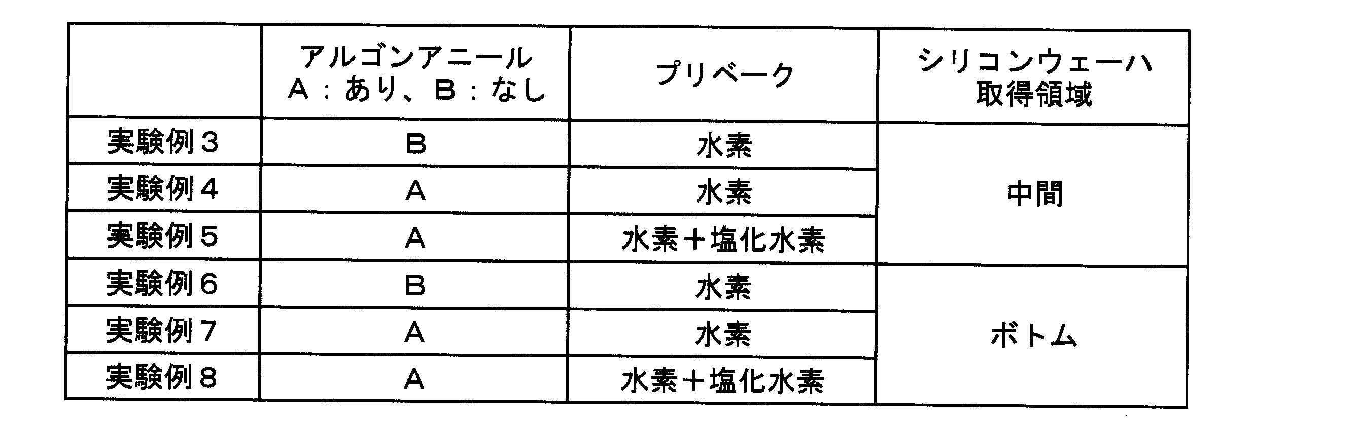
まず、実験例3と実験例6とを比較すると、中間領域のSFがボトム領域より多いことがわかる。
これは、単結晶インゴット製造時の熱履歴の影響により、中間領域のクラスターの密度がボトム領域よりも高くなるためと考えられる。
この理由は、以下のように考えられる。まず、特許文献2に記載されているように、アルゴンアニール処理を行うことで、所定厚さの表層に存在するクラスターが溶体化して少なくなる。このため、アルゴンアニール処理後に水素ガス雰囲気下でプリベーク処理を行う場合、アルゴンアニール処理を行わない場合と比べて、表層に存在するクラスターの個数が少なくなり、プリベーク処理後の微小ピットの個数も少なくなるため、SFも少なくなると考えられる。
これは、アルゴンアニール処理前の中間領域のクラスター密度がボトム領域より高いため、アルゴンアニール処理によりクラスターを溶体化しても、中間領域の方がアルゴンアニール処理後に表層に残るクラスターの個数が多くなり、クラスターが原因で発生するSFも多くなるためと考えられる。
この理由は、以下のように考えられる。まず、水素のみでプリベーク処理を行う場合、シリコンウェーハの最表層に存在するクラスターが選択的にエッチングされ、表面ピットとして顕在化し易くなる。一方、水素および塩化水素でプリベーク処理を行う場合、クラスターに加えて最表層もエッチングされる。このため、プリベーク処理を水素および塩化水素で行う場合、水素のみで行う場合と比べて、プリベーク処理後に形成される微小ピットの個数が少なくなり、SFも少なくなると考えられる。
これは、アルゴンアニール処理によりクラスターが溶体化する表層の厚さが、クラスター密度にかかわらずほぼ同じであり、プリベーク処理のエッチングによる表層の取代が、アルゴンアニール処理によりクラスターが溶体化する表層の厚さより小さければ、プリベーク処理後の表層に存在する微小ピットの個数も同じになるためと考えられる。
なお、単結晶インゴットにおけるSFが最も多い中間領域でさえも、プリベーク処理を水素および塩化水素で行うことで、SFの個数を0.02個/cm2以下に減らせることから、単結晶インゴットの他の領域から取得したシリコンウェーハに対して当該プリベーク処理を行っても、SFの個数を同レベルに減らすことができると考えられる。
本発明は、上述のような知見に基づいて完成されたものである。
ここで、水素および塩化水素でのプリベーク処理による表層の取代が、アルゴンアニール処理によりクラスターが溶体化する表層の厚さより大きい場合、プリベーク処理後の新しい表層に、アルゴンアニール処理で溶解化していないクラスターが存在し、このクラスターが選択的にエッチングされることで微小ピットが形成され、SFが発生する可能性がある。
そこで、水素および塩化水素でのプリベーク処理による表層の取代の最適値を決定するための実験を行った。また、エピタキシャル膜の成長温度の最適値を決定するための実験を合わせて行った。
次に、水素および塩化水素でのプリベーク処理の熱処理時間、熱処理温度、塩化水素ガスの濃度等を調整することで、表層の取代がそれぞれ50nm、100nm、150nm、180nm、290nm、395nmのシリコンウェーハを複数ずつ準備した。なお、シリコンウェーハの裏面にポリシリコン膜を設けずに、アルゴンアニール処理やプリベーク処理を行った。
その後、上述したそれぞれの取代のシリコンウェーハに対し、成長温度を1060℃、1080℃、1100℃としたこと以外は、実験例2と同じ条件でエピタキシャル膜を成長させ、エピタキシャルシリコンウェーハを製造し、SFの個数を調べた。その結果を図5に示す。
この理由は、取代が100nm未満の場合、表層に存在するクラスターの深さ方向の寸法よりも取代が少ないため、クラスター全体を除去することができず、除去されずに残った部分に起因する微小ピットが形成されるためと考えられる。
一方、取代が300nmより大きい場合、アルゴンアニール処理によりクラスターが溶体化する表層の厚さよりも取代が大きいため、プリベーク処理後の新しい表層に、アルゴンアニール処理で溶解化していないクラスターが存在し、このクラスターに起因する微小ピットが形成されるためと考えられる。
さらに、取代が100nm以上200nm以下の場合、エピタキシャル膜の成長温度が1080℃および1060℃のときには、SFの個数が0.03個/cm2以下になることが分かった。
本発明のエピタキシャルシリコンウェーハの製造方法において、前記アルゴンアニール工程は、アルゴンガス雰囲気下において1150℃以上1250℃以下の温度で熱処理を行う工程であり、前記プリベーク工程は、水素および塩化水素を含むガス雰囲気下において1050℃以上1250℃以下の温度で熱処理を行う工程であることが好ましい。
本発明のエピタキシャルシリコンウェーハの製造方法において、前記エピタキシャル膜成長工程は、1050℃以上1150℃以下の温度で前記エピタキシャル膜を成長させることが好ましく、特に1080℃以下の温度でエピタキシャル膜を成長させることが好ましい。
ここで、1050℃未満の水素ガス雰囲気下に塩化水素ガスを供給した場合、エピタキシャルシリコンウェーハに曇りが発生してしまうことが実験的に確認されている。また、1250℃より高い温度の水素ガス雰囲気下に塩化水素ガスを供給した場合、熱応力が大きくなるため、ウェーハに反りが発生し、スリップ転位が発生し易くなってしまう不具合がある。
本発明によれば、1050℃以上1250℃以下の水素ガス雰囲気下に塩化水素ガスを供給することで、エピタキシャルシリコンウェーハに曇りが発生してしまうことと、スリップ転位の発生を抑制することができる。
図6に示すように、エピタキシャルシリコンウェーハの製造方法では、単結晶インゴット製造工程を行う(ステップS1)。
この単結晶インゴット製造工程では、図示しない引き上げ装置を用いたCZ法(チョクラルスキー法)にて、n型ドーパントとして赤リンを添加したシリコン融液から、直径200mmの単結晶インゴットを製造する。
ここで、単結晶インゴットから切り出されたシリコンウェーハの抵抗率が0.6mΩ・cm以上0.98mΩ・cm以下となるように、以下の条件で単結晶インゴットを製造した。
赤リン濃度:7.54×10¹⁹atoms/cm3以上1.32×1020atoms/cm3以下
酸素濃度:7×10¹⁷atoms/cm3以上12×1017atoms/cm3以下
なお、ミスフィット転移を抑制するために、3.70×10¹⁹atoms/cm3以上2.93×1020atoms/cm3以下の濃度のゲルマニウムを添加してもよい。
原料ガス:モノシラン(SiH4)と酸素(O2)の混合ガス
裏面酸化膜の厚さ:550nm(100nm以上1500nm以下)
成膜温度:430℃(400℃以上450℃以下)
このような裏面酸化膜を設けることによって、オートドープ現象が抑制される。
このように裏面酸化膜の外周部を除去することによって、ノジュールの発生が抑制される。
雰囲気:アルゴンガス
熱処理温度:1200℃~1220℃(1150℃以上1250℃以下)
熱処理時間:30分以上120分以下
このようなアルゴンアニール工程を行うことによって、シリコンウェーハに発生しているクラスターが溶体化して少なくなる。
なお、アルゴンアニール工程において赤リンが外方拡散することで、シリコンウェーハの表面には、厚さが0.65μm以上0.91μm以下の外方拡散層が形成され、遷移領域幅が増大してしまう。しかし、その後のデバイス製造時における熱処理によって、濃度の高い位置から低い位置に赤リンが移動するため、問題とはならない。
雰囲気:水素ガス、塩化水素ガス
水素ガスの流量:40L/分
塩化水素ガスの流量:1L/分
熱処理温度:1190℃(1050℃以上1250℃以下)
熱処理時間:30秒(30秒以上300秒以下)
なお、プリベーク工程において水素および塩化水素を含むガス雰囲気を形成するに際し、まず水素ガスのみの雰囲気下で昇温し、1050℃以上1250℃以下の温度に到達したら、塩化水素ガスを供給することが好ましい。このようなタイミングで塩化水素ガスを供給することによって、エピタキシャルシリコンウェーハに曇りが発生してしまうことと、スリップ転位の発生を抑制することができる。
また、プリベーク工程によるシリコンウェーハの取代は、100nm以上300nmであることが好ましく、150nm±10nmであることがさらに好ましい。
ドーパントガス:フォスフィン(PH3)ガス
原料ソースガス:トリクロロシラン(SiHCl3)ガス
キャリアガス:水素ガス
成長温度:1060℃(1050℃以上1150℃以下)
エピタキシャル膜の厚さ:4μm(1μm以上10μm以下)
抵抗率(エピ膜抵抗率):0.3Ω・cm(0.01Ω・cm以上10Ω・cm以下)
赤リン濃度:1.87×10¹⁶atoms/cm3(4.44×1014atoms/cm3以上4.53×1018atoms/cm3以下)
このようなエピタキシャル膜成長工程を行うことによって、シリコンウェーハの表面にエピタキシャル膜が形成されたエピタキシャルシリコンウェーハが製造される。
さらには、裏面酸化膜除去工程を行ってからアルゴンアニール工程を行うため、裏面酸化膜で覆われていない外周部からの赤リンの外方拡散を促進させることができ、オートドープ現象の発生を抑制できる。このため、エピタキシャル膜面内の抵抗率の均一化を図れる。
なお、本発明は上記実施形態にのみ限定されるものではなく、本発明の要旨を逸脱しない範囲内において種々の改良ならびに設計の変更などが可能である。
例えば、リンが添加された単結晶インゴットから取得されたシリコンウェーハであれば、抵抗率が0.98mΩ・cmより大きいシリコンウェーハ(例えば抵抗率が1.5mΩ・cm以下)に対し、本発明のエピタキシャルシリコンウェーハの製造方法を適用してもよい。
また、アルゴンアニール工程と、水素のみでのプリベーク工程とを行った場合のSFの発生個数を予測できる場合には、予測個数が許容値以上のシリコンウェーハに対して、アルゴンアニール工程後に水素および塩化水素でのプリベーク工程を行い、前記許容値未満のシリコンウェーハに対して、アルゴンアニール工程後に水素のみでのプリベーク工程を行ってもよい。なお、SFの発生個数の予測は、単結晶インゴットの熱履歴に基づき行ってもよいし、上記特許文献2のように、所定位置から切り出した評価用シリコンウェーハのピット評価用熱処理を用いた評価結果に基づき行ってもよい。
Claims (5)
- リンが添加されたシリコンウェーハの表面にエピタキシャル膜が設けられたエピタキシャルシリコンウェーハの製造方法であって、
CZ法により製造された単結晶インゴットから切り出されたシリコンウェーハの裏面に酸化膜を形成する裏面酸化膜形成工程と、
前記シリコンウェーハの外周部に存在する前記酸化膜を除去する裏面酸化膜除去工程と、
前記裏面酸化膜除去工程後の前記シリコンウェーハに対し、アルゴンガス雰囲気下において熱処理を行うアルゴンアニール工程と、
前記アルゴンアニール工程後の前記シリコンウェーハの表面にエピタキシャル膜を形成するエピタキシャル膜形成工程とを備え、
前記エピタキシャル膜形成工程は、前記シリコンウェーハに対し、水素および塩化水素を含むガス雰囲気下において熱処理を行うことで、前記シリコンウェーハの表層をエッチングするプリベーク工程と、
前記プリベーク工程後の前記シリコンウェーハの表面に前記エピタキシャル膜を成長させるエピタキシャル膜成長工程とを有することを特徴とするエピタキシャルシリコンウェーハの製造方法。 - 請求項1に記載のエピタキシャルシリコンウェーハの製造方法において、
前記プリベーク工程は、厚さが100nm以上300nm以下の前記表層をエッチングすることを特徴とするエピタキシャルシリコンウェーハの製造方法。 - 請求項1または請求項2に記載のエピタキシャルシリコンウェーハの製造方法において、
前記アルゴンアニール工程は、アルゴンガス雰囲気下において1150℃以上1250℃以下の温度で熱処理を行う工程であり、
前記プリベーク工程は、水素および塩化水素を含むガス雰囲気下において1050℃以上1250℃以下の温度で熱処理を行う工程であることを特徴とするエピタキシャルシリコンウェーハの製造方法。 - 請求項1から請求項3のいずれか一項に記載のエピタキシャルシリコンウェーハの製造方法において、
前記エピタキシャル膜成長工程は、1050℃以上1150℃以下の温度で前記エピタキシャル膜を成長させることを特徴とするエピタキシャルシリコンウェーハの製造方法。 - 請求項1から請求項4のいずれか一項に記載のエピタキシャルシリコンウェーハの製造方法において、
前記シリコンウェーハの抵抗率は、1.5mΩ・cm以下であることを特徴とするエピタキシャルシリコンウェーハの製造方法。
Priority Applications (4)
| Application Number | Priority Date | Filing Date | Title |
|---|---|---|---|
| DE112016001962.9T DE112016001962T5 (de) | 2015-04-30 | 2016-04-05 | Verfahren zur Herstellung von Siliziumepitaxialwafern |
| US15/568,158 US10253429B2 (en) | 2015-04-30 | 2016-04-05 | Method for manufacturing epitaxial silicon wafer |
| KR1020177029422A KR102036596B1 (ko) | 2015-04-30 | 2016-04-05 | 에피택셜 실리콘 웨이퍼의 제조 방법 |
| CN201680024967.0A CN107533959B (zh) | 2015-04-30 | 2016-04-05 | 外延硅晶片的制造方法 |
Applications Claiming Priority (2)
| Application Number | Priority Date | Filing Date | Title |
|---|---|---|---|
| JP2015092805A JP6477210B2 (ja) | 2015-04-30 | 2015-04-30 | エピタキシャルシリコンウェーハの製造方法 |
| JP2015-092805 | 2015-04-30 |
Publications (1)
| Publication Number | Publication Date |
|---|---|
| WO2016174997A1 true WO2016174997A1 (ja) | 2016-11-03 |
Family
ID=57198427
Family Applications (1)
| Application Number | Title | Priority Date | Filing Date |
|---|---|---|---|
| PCT/JP2016/061088 Ceased WO2016174997A1 (ja) | 2015-04-30 | 2016-04-05 | エピタキシャルシリコンウェーハの製造方法 |
Country Status (7)
| Country | Link |
|---|---|
| US (1) | US10253429B2 (ja) |
| JP (1) | JP6477210B2 (ja) |
| KR (1) | KR102036596B1 (ja) |
| CN (1) | CN107533959B (ja) |
| DE (1) | DE112016001962T5 (ja) |
| TW (1) | TWI624861B (ja) |
| WO (1) | WO2016174997A1 (ja) |
Cited By (2)
| Publication number | Priority date | Publication date | Assignee | Title |
|---|---|---|---|---|
| WO2018186248A1 (ja) * | 2017-04-06 | 2018-10-11 | 株式会社Sumco | エピタキシャルシリコンウェーハの製造方法およびエピタキシャルシリコンウェーハ |
| CN109509704A (zh) * | 2017-09-15 | 2019-03-22 | 胜高股份有限公司 | 外延硅晶片的制备方法及外延硅晶片 |
Families Citing this family (18)
| Publication number | Priority date | Publication date | Assignee | Title |
|---|---|---|---|---|
| JP6358472B2 (ja) * | 2015-06-08 | 2018-07-18 | 信越半導体株式会社 | エピタキシャルウェーハの製造方法 |
| JP6432879B2 (ja) * | 2015-11-13 | 2018-12-05 | 信越半導体株式会社 | エピタキシャルウェーハの製造方法 |
| JP6447960B2 (ja) * | 2016-04-01 | 2019-01-09 | 信越半導体株式会社 | シリコンエピタキシャルウェーハの製造方法 |
| JP6598140B2 (ja) * | 2016-05-19 | 2019-10-30 | 信越半導体株式会社 | エピタキシャルウェーハの製造方法 |
| JP7080017B2 (ja) | 2017-04-25 | 2022-06-03 | 株式会社Sumco | n型シリコン単結晶のインゴット、シリコンウェーハ、およびエピタキシャルシリコンウェーハ |
| DE112018002163B4 (de) * | 2017-04-25 | 2022-12-15 | Sumco Corporation | Verfahren zur Herstellung eines Silicium-Einkristalls, Verfahren zur Herstellung eines epitaktischen Silicium-Wafers, Silicium-Einkristall, und epitaktischer Silicium-Wafer |
| JP6835006B2 (ja) * | 2018-02-16 | 2021-02-24 | 株式会社Sumco | エピタキシャルシリコンウェーハにおける積層欠陥の発生予測方法及びエピタキシャルシリコンウェーハの製造方法 |
| US10559479B2 (en) | 2018-02-27 | 2020-02-11 | Toshiba Memory Corporation | Semiconductor manufacturing apparatus and manufacturing method of semiconductor device |
| US11295949B2 (en) | 2019-04-01 | 2022-04-05 | Vishay SIliconix, LLC | Virtual wafer techniques for fabricating semiconductor devices |
| JP7491705B2 (ja) * | 2020-02-19 | 2024-05-28 | グローバルウェーハズ・ジャパン株式会社 | 半導体シリコンウェーハの製造方法 |
| JP7519784B2 (ja) * | 2020-02-19 | 2024-07-22 | グローバルウェーハズ・ジャパン株式会社 | シリコンウェーハの製造方法 |
| JP7495238B2 (ja) | 2020-02-19 | 2024-06-04 | グローバルウェーハズ・ジャパン株式会社 | シリコンウェーハの製造方法 |
| JP7272343B2 (ja) * | 2020-12-01 | 2023-05-12 | 株式会社Sumco | n型シリコン単結晶の製造方法 |
| TWI854344B (zh) * | 2021-11-04 | 2024-09-01 | 日商Sumco股份有限公司 | 矽晶圓及磊晶矽晶圓 |
| JP7658332B2 (ja) * | 2021-11-04 | 2025-04-08 | 株式会社Sumco | シリコンウェーハおよびエピタキシャルシリコンウェーハ |
| JP7770907B2 (ja) * | 2021-12-22 | 2025-11-17 | グローバルウェーハズ・ジャパン株式会社 | シリコンエピタキシャル基板の製造方法およびシリコンエピタキシャル基板 |
| CN116065239A (zh) * | 2022-12-15 | 2023-05-05 | 西安奕斯伟材料科技有限公司 | 硅片的处理方法 |
| CN118127626B (zh) * | 2024-02-21 | 2025-09-23 | 中环领先半导体科技股份有限公司 | 一种外延片及其制备方法 |
Citations (7)
| Publication number | Priority date | Publication date | Assignee | Title |
|---|---|---|---|---|
| JPH0472718A (ja) * | 1990-07-13 | 1992-03-06 | Nec Corp | エピタキシャル成長方法 |
| JP2004091234A (ja) * | 2002-08-30 | 2004-03-25 | Sumitomo Mitsubishi Silicon Corp | エピタキシャルウェーハとその製造方法 |
| JP2004363510A (ja) * | 2003-06-09 | 2004-12-24 | Sumitomo Mitsubishi Silicon Corp | 半導体基板の製造方法 |
| JP2007088469A (ja) * | 2005-09-22 | 2007-04-05 | Siltronic Ag | エピタキシャルシリコンウェハおよびエピタキシャルシリコンウェハの製造方法 |
| JP2011142327A (ja) * | 2006-11-22 | 2011-07-21 | Siltronic Ag | 前面および背面を有する半導体ウェハ |
| JP2012164814A (ja) * | 2011-02-07 | 2012-08-30 | Sumco Corp | エピタキシャルウェーハの製造方法 |
| JP2014011293A (ja) * | 2012-06-29 | 2014-01-20 | Sumco Corp | エピタキシャルシリコンウェーハの製造方法、および、エピタキシャルシリコンウェーハ |
Family Cites Families (12)
| Publication number | Priority date | Publication date | Assignee | Title |
|---|---|---|---|---|
| NL187414C (nl) * | 1978-04-21 | 1991-09-16 | Philips Nv | Werkwijze voor het aanbrengen van een epitaxiale laag. |
| JP4089809B2 (ja) | 2002-03-13 | 2008-05-28 | Sumco Techxiv株式会社 | 半導体ウェーハのエッジ部の酸化膜除去装置 |
| GB2409340B (en) * | 2002-10-04 | 2006-05-10 | Silicon Genesis Corp | Method for treating semiconductor material |
| US7396743B2 (en) * | 2004-06-10 | 2008-07-08 | Singh Kaushal K | Low temperature epitaxial growth of silicon-containing films using UV radiation |
| DE102005045339B4 (de) * | 2005-09-22 | 2009-04-02 | Siltronic Ag | Epitaxierte Siliciumscheibe und Verfahren zur Herstellung von epitaxierten Siliciumscheiben |
| KR100793607B1 (ko) * | 2006-06-27 | 2008-01-10 | 매그나칩 반도체 유한회사 | 에피텍셜 실리콘 웨이퍼 및 그 제조방법 |
| DE102008026784A1 (de) * | 2008-06-04 | 2009-12-10 | Siltronic Ag | Epitaxierte Siliciumscheibe mit <110>-Kristallorientierung und Verfahren zu ihrer Herstellung |
| JP5445075B2 (ja) | 2009-11-27 | 2014-03-19 | 株式会社Sumco | エピタキシャルウェーハの製造方法 |
| JP6009237B2 (ja) | 2012-06-18 | 2016-10-19 | Sumco Techxiv株式会社 | エピタキシャルシリコンウェーハの製造方法、および、エピタキシャルシリコンウェーハ |
| US10233562B2 (en) | 2013-04-24 | 2019-03-19 | Sumco Techxiv Corporation | Method for producing single crystal, and method for producing silicon wafer |
| CN103489761A (zh) * | 2013-09-17 | 2014-01-01 | 杭州立昂微电子股份有限公司 | 一种肖特基芯片专用外延片的生长方法 |
| CN103887176B (zh) * | 2014-03-20 | 2016-08-24 | 上海华力微电子有限公司 | 一种降低源漏外延生长缺陷的方法 |
-
2015
- 2015-04-30 JP JP2015092805A patent/JP6477210B2/ja active Active
-
2016
- 2016-03-31 TW TW105110247A patent/TWI624861B/zh active
- 2016-04-05 WO PCT/JP2016/061088 patent/WO2016174997A1/ja not_active Ceased
- 2016-04-05 KR KR1020177029422A patent/KR102036596B1/ko active Active
- 2016-04-05 US US15/568,158 patent/US10253429B2/en active Active
- 2016-04-05 DE DE112016001962.9T patent/DE112016001962T5/de active Granted
- 2016-04-05 CN CN201680024967.0A patent/CN107533959B/zh active Active
Patent Citations (7)
| Publication number | Priority date | Publication date | Assignee | Title |
|---|---|---|---|---|
| JPH0472718A (ja) * | 1990-07-13 | 1992-03-06 | Nec Corp | エピタキシャル成長方法 |
| JP2004091234A (ja) * | 2002-08-30 | 2004-03-25 | Sumitomo Mitsubishi Silicon Corp | エピタキシャルウェーハとその製造方法 |
| JP2004363510A (ja) * | 2003-06-09 | 2004-12-24 | Sumitomo Mitsubishi Silicon Corp | 半導体基板の製造方法 |
| JP2007088469A (ja) * | 2005-09-22 | 2007-04-05 | Siltronic Ag | エピタキシャルシリコンウェハおよびエピタキシャルシリコンウェハの製造方法 |
| JP2011142327A (ja) * | 2006-11-22 | 2011-07-21 | Siltronic Ag | 前面および背面を有する半導体ウェハ |
| JP2012164814A (ja) * | 2011-02-07 | 2012-08-30 | Sumco Corp | エピタキシャルウェーハの製造方法 |
| JP2014011293A (ja) * | 2012-06-29 | 2014-01-20 | Sumco Corp | エピタキシャルシリコンウェーハの製造方法、および、エピタキシャルシリコンウェーハ |
Cited By (8)
| Publication number | Priority date | Publication date | Assignee | Title |
|---|---|---|---|---|
| WO2018186248A1 (ja) * | 2017-04-06 | 2018-10-11 | 株式会社Sumco | エピタキシャルシリコンウェーハの製造方法およびエピタキシャルシリコンウェーハ |
| KR20190124793A (ko) * | 2017-04-06 | 2019-11-05 | 가부시키가이샤 사무코 | 에피택셜 실리콘 웨이퍼의 제조 방법 및 에피택셜 실리콘 웨이퍼 |
| CN110603350A (zh) * | 2017-04-06 | 2019-12-20 | 胜高股份有限公司 | 外延硅晶片的制造方法及外延硅晶片 |
| JPWO2018186248A1 (ja) * | 2017-04-06 | 2020-01-16 | 株式会社Sumco | エピタキシャルシリコンウェーハの製造方法およびエピタキシャルシリコンウェーハ |
| US10867791B2 (en) | 2017-04-06 | 2020-12-15 | Sumco Corporation | Method for manufacturing epitaxial silicon wafer and epitaxial silicon wafer |
| CN110603350B (zh) * | 2017-04-06 | 2021-07-16 | 胜高股份有限公司 | 外延硅晶片的制造方法及外延硅晶片 |
| KR102279113B1 (ko) * | 2017-04-06 | 2021-07-16 | 가부시키가이샤 사무코 | 에피택셜 실리콘 웨이퍼의 제조 방법 및 에피택셜 실리콘 웨이퍼 |
| CN109509704A (zh) * | 2017-09-15 | 2019-03-22 | 胜高股份有限公司 | 外延硅晶片的制备方法及外延硅晶片 |
Also Published As
| Publication number | Publication date |
|---|---|
| KR102036596B1 (ko) | 2019-10-25 |
| US10253429B2 (en) | 2019-04-09 |
| JP2016213232A (ja) | 2016-12-15 |
| DE112016001962T5 (de) | 2018-01-18 |
| TW201705219A (zh) | 2017-02-01 |
| TWI624861B (zh) | 2018-05-21 |
| US20180087184A1 (en) | 2018-03-29 |
| JP6477210B2 (ja) | 2019-03-06 |
| KR20170126498A (ko) | 2017-11-17 |
| CN107533959B (zh) | 2020-09-29 |
| CN107533959A (zh) | 2018-01-02 |
Similar Documents
| Publication | Publication Date | Title |
|---|---|---|
| JP6477210B2 (ja) | エピタキシャルシリコンウェーハの製造方法 | |
| JP5845143B2 (ja) | エピタキシャルシリコンウェーハの製造方法、および、エピタキシャルシリコンウェーハ | |
| JP2014011293A5 (ja) | ||
| US10211066B2 (en) | Silicon epitaxial wafer and method of producing same | |
| TW201527610A (zh) | 矽晶圓及其製造方法 | |
| WO2021166896A1 (ja) | 半導体シリコンウェーハの製造方法 | |
| JP5533869B2 (ja) | エピタキシャルシリコンウェーハとその製造方法 | |
| TWI741950B (zh) | 矽晶圓的製造方法 | |
| US20200020817A1 (en) | Epitaxial silicon wafer | |
| JP2025157587A (ja) | シリコンウェーハおよびエピタキシャルシリコンウェーハ | |
| WO2018186248A1 (ja) | エピタキシャルシリコンウェーハの製造方法およびエピタキシャルシリコンウェーハ | |
| JP7757917B2 (ja) | シリコンウェーハおよびエピタキシャルシリコンウェーハ | |
| JP7757916B2 (ja) | シリコンウェーハおよびエピタキシャルシリコンウェーハ | |
| CN115135818B (zh) | 半导体硅晶片的制造方法 | |
| JP6432879B2 (ja) | エピタキシャルウェーハの製造方法 | |
| JP2011155130A (ja) | エピタキシャルウェーハ及びその製造方法 | |
| JP6598140B2 (ja) | エピタキシャルウェーハの製造方法 | |
| JP7775800B2 (ja) | シリコンウェーハおよびエピタキシャルシリコンウェーハ | |
| US12527054B2 (en) | Silicon wafer and epitaxial silicon wafer |
Legal Events
| Date | Code | Title | Description |
|---|---|---|---|
| 121 | Ep: the epo has been informed by wipo that ep was designated in this application |
Ref document number: 16786274 Country of ref document: EP Kind code of ref document: A1 |
|
| ENP | Entry into the national phase |
Ref document number: 20177029422 Country of ref document: KR Kind code of ref document: A |
|
| WWE | Wipo information: entry into national phase |
Ref document number: 15568158 Country of ref document: US |
|
| WWE | Wipo information: entry into national phase |
Ref document number: 112016001962 Country of ref document: DE |
|
| 122 | Ep: pct application non-entry in european phase |
Ref document number: 16786274 Country of ref document: EP Kind code of ref document: A1 |