WO2014163058A1 - 半導体装置 - Google Patents
半導体装置 Download PDFInfo
- Publication number
- WO2014163058A1 WO2014163058A1 PCT/JP2014/059578 JP2014059578W WO2014163058A1 WO 2014163058 A1 WO2014163058 A1 WO 2014163058A1 JP 2014059578 W JP2014059578 W JP 2014059578W WO 2014163058 A1 WO2014163058 A1 WO 2014163058A1
- Authority
- WO
- WIPO (PCT)
- Prior art keywords
- layer
- semiconductor device
- gate
- diffusion region
- region
- Prior art date
- Legal status (The legal status is an assumption and is not a legal conclusion. Google has not performed a legal analysis and makes no representation as to the accuracy of the status listed.)
- Ceased
Links
Images









Classifications
-
- H—ELECTRICITY
- H10—SEMICONDUCTOR DEVICES; ELECTRIC SOLID-STATE DEVICES NOT OTHERWISE PROVIDED FOR
- H10D—INORGANIC ELECTRIC SEMICONDUCTOR DEVICES
- H10D30/00—Field-effect transistors [FET]
- H10D30/60—Insulated-gate field-effect transistors [IGFET]
- H10D30/64—Double-diffused metal-oxide semiconductor [DMOS] FETs
- H10D30/66—Vertical DMOS [VDMOS] FETs
-
- H—ELECTRICITY
- H10—SEMICONDUCTOR DEVICES; ELECTRIC SOLID-STATE DEVICES NOT OTHERWISE PROVIDED FOR
- H10D—INORGANIC ELECTRIC SEMICONDUCTOR DEVICES
- H10D12/00—Bipolar devices controlled by the field effect, e.g. insulated-gate bipolar transistors [IGBT]
- H10D12/411—Insulated-gate bipolar transistors [IGBT]
- H10D12/441—Vertical IGBTs
- H10D12/461—Vertical IGBTs having non-planar surfaces, e.g. having trenches, recesses or pillars in the surfaces of the emitter, base or collector regions
- H10D12/481—Vertical IGBTs having non-planar surfaces, e.g. having trenches, recesses or pillars in the surfaces of the emitter, base or collector regions having gate structures on slanted surfaces, on vertical surfaces, or in grooves, e.g. trench gate IGBTs
-
- H—ELECTRICITY
- H10—SEMICONDUCTOR DEVICES; ELECTRIC SOLID-STATE DEVICES NOT OTHERWISE PROVIDED FOR
- H10D—INORGANIC ELECTRIC SEMICONDUCTOR DEVICES
- H10D30/00—Field-effect transistors [FET]
- H10D30/01—Manufacture or treatment
- H10D30/021—Manufacture or treatment of FETs having insulated gates [IGFET]
- H10D30/028—Manufacture or treatment of FETs having insulated gates [IGFET] of double-diffused metal oxide semiconductor [DMOS] FETs
- H10D30/0291—Manufacture or treatment of FETs having insulated gates [IGFET] of double-diffused metal oxide semiconductor [DMOS] FETs of vertical DMOS [VDMOS] FETs
-
- H—ELECTRICITY
- H10—SEMICONDUCTOR DEVICES; ELECTRIC SOLID-STATE DEVICES NOT OTHERWISE PROVIDED FOR
- H10D—INORGANIC ELECTRIC SEMICONDUCTOR DEVICES
- H10D30/00—Field-effect transistors [FET]
- H10D30/60—Insulated-gate field-effect transistors [IGFET]
- H10D30/64—Double-diffused metal-oxide semiconductor [DMOS] FETs
- H10D30/66—Vertical DMOS [VDMOS] FETs
- H10D30/662—Vertical DMOS [VDMOS] FETs having a drift region having a doping concentration that is higher between adjacent body regions relative to other parts of the drift region
-
- H—ELECTRICITY
- H10—SEMICONDUCTOR DEVICES; ELECTRIC SOLID-STATE DEVICES NOT OTHERWISE PROVIDED FOR
- H10D—INORGANIC ELECTRIC SEMICONDUCTOR DEVICES
- H10D30/00—Field-effect transistors [FET]
- H10D30/60—Insulated-gate field-effect transistors [IGFET]
- H10D30/64—Double-diffused metal-oxide semiconductor [DMOS] FETs
- H10D30/66—Vertical DMOS [VDMOS] FETs
- H10D30/665—Vertical DMOS [VDMOS] FETs having edge termination structures
-
- H—ELECTRICITY
- H10—SEMICONDUCTOR DEVICES; ELECTRIC SOLID-STATE DEVICES NOT OTHERWISE PROVIDED FOR
- H10D—INORGANIC ELECTRIC SEMICONDUCTOR DEVICES
- H10D30/00—Field-effect transistors [FET]
- H10D30/60—Insulated-gate field-effect transistors [IGFET]
- H10D30/64—Double-diffused metal-oxide semiconductor [DMOS] FETs
- H10D30/66—Vertical DMOS [VDMOS] FETs
- H10D30/668—Vertical DMOS [VDMOS] FETs having trench gate electrodes, e.g. UMOS transistors
-
- H—ELECTRICITY
- H10—SEMICONDUCTOR DEVICES; ELECTRIC SOLID-STATE DEVICES NOT OTHERWISE PROVIDED FOR
- H10D—INORGANIC ELECTRIC SEMICONDUCTOR DEVICES
- H10D62/00—Semiconductor bodies, or regions thereof, of devices having potential barriers
- H10D62/10—Shapes, relative sizes or dispositions of the regions of the semiconductor bodies; Shapes of the semiconductor bodies
- H10D62/102—Constructional design considerations for preventing surface leakage or controlling electric field concentration
- H10D62/103—Constructional design considerations for preventing surface leakage or controlling electric field concentration for increasing or controlling the breakdown voltage of reverse-biased devices
- H10D62/105—Constructional design considerations for preventing surface leakage or controlling electric field concentration for increasing or controlling the breakdown voltage of reverse-biased devices by having particular doping profiles, shapes or arrangements of PN junctions; by having supplementary regions, e.g. junction termination extension [JTE]
- H10D62/106—Constructional design considerations for preventing surface leakage or controlling electric field concentration for increasing or controlling the breakdown voltage of reverse-biased devices by having particular doping profiles, shapes or arrangements of PN junctions; by having supplementary regions, e.g. junction termination extension [JTE] having supplementary regions doped oppositely to or in rectifying contact with regions of the semiconductor bodies, e.g. guard rings with PN or Schottky junctions
-
- H—ELECTRICITY
- H10—SEMICONDUCTOR DEVICES; ELECTRIC SOLID-STATE DEVICES NOT OTHERWISE PROVIDED FOR
- H10D—INORGANIC ELECTRIC SEMICONDUCTOR DEVICES
- H10D62/00—Semiconductor bodies, or regions thereof, of devices having potential barriers
- H10D62/10—Shapes, relative sizes or dispositions of the regions of the semiconductor bodies; Shapes of the semiconductor bodies
- H10D62/102—Constructional design considerations for preventing surface leakage or controlling electric field concentration
- H10D62/103—Constructional design considerations for preventing surface leakage or controlling electric field concentration for increasing or controlling the breakdown voltage of reverse-biased devices
- H10D62/105—Constructional design considerations for preventing surface leakage or controlling electric field concentration for increasing or controlling the breakdown voltage of reverse-biased devices by having particular doping profiles, shapes or arrangements of PN junctions; by having supplementary regions, e.g. junction termination extension [JTE]
- H10D62/109—Reduced surface field [RESURF] PN junction structures
- H10D62/111—Multiple RESURF structures, e.g. double RESURF or 3D-RESURF structures
-
- H—ELECTRICITY
- H10—SEMICONDUCTOR DEVICES; ELECTRIC SOLID-STATE DEVICES NOT OTHERWISE PROVIDED FOR
- H10D—INORGANIC ELECTRIC SEMICONDUCTOR DEVICES
- H10D62/00—Semiconductor bodies, or regions thereof, of devices having potential barriers
- H10D62/10—Shapes, relative sizes or dispositions of the regions of the semiconductor bodies; Shapes of the semiconductor bodies
- H10D62/124—Shapes, relative sizes or dispositions of the regions of semiconductor bodies or of junctions between the regions
- H10D62/126—Top-view geometrical layouts of the regions or the junctions
- H10D62/127—Top-view geometrical layouts of the regions or the junctions of cellular field-effect devices, e.g. multicellular DMOS transistors or IGBTs
-
- H—ELECTRICITY
- H10—SEMICONDUCTOR DEVICES; ELECTRIC SOLID-STATE DEVICES NOT OTHERWISE PROVIDED FOR
- H10D—INORGANIC ELECTRIC SEMICONDUCTOR DEVICES
- H10D62/00—Semiconductor bodies, or regions thereof, of devices having potential barriers
- H10D62/10—Shapes, relative sizes or dispositions of the regions of the semiconductor bodies; Shapes of the semiconductor bodies
- H10D62/13—Semiconductor regions connected to electrodes carrying current to be rectified, amplified or switched, e.g. source or drain regions
- H10D62/149—Source or drain regions of field-effect devices
- H10D62/151—Source or drain regions of field-effect devices of IGFETs
- H10D62/152—Source regions of DMOS transistors
- H10D62/153—Impurity concentrations or distributions
-
- H—ELECTRICITY
- H10—SEMICONDUCTOR DEVICES; ELECTRIC SOLID-STATE DEVICES NOT OTHERWISE PROVIDED FOR
- H10D—INORGANIC ELECTRIC SEMICONDUCTOR DEVICES
- H10D64/00—Electrodes of devices having potential barriers
- H10D64/118—Electrodes comprising insulating layers having particular dielectric or electrostatic properties, e.g. having static charges
-
- H—ELECTRICITY
- H10—SEMICONDUCTOR DEVICES; ELECTRIC SOLID-STATE DEVICES NOT OTHERWISE PROVIDED FOR
- H10D—INORGANIC ELECTRIC SEMICONDUCTOR DEVICES
- H10D64/00—Electrodes of devices having potential barriers
- H10D64/20—Electrodes characterised by their shapes, relative sizes or dispositions
- H10D64/27—Electrodes not carrying the current to be rectified, amplified, oscillated or switched, e.g. gates
- H10D64/311—Gate electrodes for field-effect devices
- H10D64/411—Gate electrodes for field-effect devices for FETs
- H10D64/511—Gate electrodes for field-effect devices for FETs for IGFETs
- H10D64/517—Gate electrodes for field-effect devices for FETs for IGFETs characterised by the conducting layers
- H10D64/518—Gate electrodes for field-effect devices for FETs for IGFETs characterised by the conducting layers characterised by their lengths or sectional shapes
-
- H—ELECTRICITY
- H10—SEMICONDUCTOR DEVICES; ELECTRIC SOLID-STATE DEVICES NOT OTHERWISE PROVIDED FOR
- H10D—INORGANIC ELECTRIC SEMICONDUCTOR DEVICES
- H10D64/00—Electrodes of devices having potential barriers
- H10D64/20—Electrodes characterised by their shapes, relative sizes or dispositions
- H10D64/27—Electrodes not carrying the current to be rectified, amplified, oscillated or switched, e.g. gates
- H10D64/311—Gate electrodes for field-effect devices
- H10D64/411—Gate electrodes for field-effect devices for FETs
- H10D64/511—Gate electrodes for field-effect devices for FETs for IGFETs
- H10D64/517—Gate electrodes for field-effect devices for FETs for IGFETs characterised by the conducting layers
- H10D64/519—Gate electrodes for field-effect devices for FETs for IGFETs characterised by the conducting layers characterised by their top-view geometrical layouts
-
- H—ELECTRICITY
- H10—SEMICONDUCTOR DEVICES; ELECTRIC SOLID-STATE DEVICES NOT OTHERWISE PROVIDED FOR
- H10D—INORGANIC ELECTRIC SEMICONDUCTOR DEVICES
- H10D84/00—Integrated devices formed in or on semiconductor substrates that comprise only semiconducting layers, e.g. on Si wafers or on GaAs-on-Si wafers
- H10D84/101—Integrated devices comprising main components and built-in components, e.g. IGBT having built-in freewheel diode
- H10D84/141—VDMOS having built-in components
-
- H—ELECTRICITY
- H10—SEMICONDUCTOR DEVICES; ELECTRIC SOLID-STATE DEVICES NOT OTHERWISE PROVIDED FOR
- H10D—INORGANIC ELECTRIC SEMICONDUCTOR DEVICES
- H10D62/00—Semiconductor bodies, or regions thereof, of devices having potential barriers
- H10D62/10—Shapes, relative sizes or dispositions of the regions of the semiconductor bodies; Shapes of the semiconductor bodies
- H10D62/13—Semiconductor regions connected to electrodes carrying current to be rectified, amplified or switched, e.g. source or drain regions
- H10D62/149—Source or drain regions of field-effect devices
- H10D62/151—Source or drain regions of field-effect devices of IGFETs
- H10D62/156—Drain regions of DMOS transistors
- H10D62/157—Impurity concentrations or distributions
-
- H—ELECTRICITY
- H10—SEMICONDUCTOR DEVICES; ELECTRIC SOLID-STATE DEVICES NOT OTHERWISE PROVIDED FOR
- H10D—INORGANIC ELECTRIC SEMICONDUCTOR DEVICES
- H10D62/00—Semiconductor bodies, or regions thereof, of devices having potential barriers
- H10D62/10—Shapes, relative sizes or dispositions of the regions of the semiconductor bodies; Shapes of the semiconductor bodies
- H10D62/17—Semiconductor regions connected to electrodes not carrying current to be rectified, amplified or switched, e.g. channel regions
- H10D62/393—Body regions of DMOS transistors or IGBTs
-
- H—ELECTRICITY
- H10—SEMICONDUCTOR DEVICES; ELECTRIC SOLID-STATE DEVICES NOT OTHERWISE PROVIDED FOR
- H10D—INORGANIC ELECTRIC SEMICONDUCTOR DEVICES
- H10D64/00—Electrodes of devices having potential barriers
- H10D64/111—Field plates
Definitions
- the present invention relates to a semiconductor device.
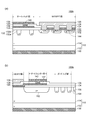
- FIG. 32 is a view shown for explaining a conventional semiconductor device 800.
- FIG. 32A is a plan view showing the main part of the semiconductor device 800
- FIG. 32B is a cross-sectional view taken along the line XX of FIG.
- the conventional semiconductor device 800 is a semiconductor device including an active element portion and a gate pad portion defined on a semiconductor substrate in which an n + drain layer 51 and an n ⁇ drift layer 52 are stacked.
- the active element section includes an n + drain layer 51, an n ⁇ drift layer 52, a p base region 53 formed on the surface of the n ⁇ drift layer 52, and a p base.
- a gate electrode 57 provided on the n + source region 54 formed on the surface of the region 53 and a p base region 53 sandwiched between the n + source region 54 and the n ⁇ drift layer 52 via a gate insulating film 56.
- a source electrode 61 provided in contact with the surfaces of the n + source region 54 and the p base region 53 while being insulated from the gate electrode 57 via the interlayer insulating film 58.
- the gate pad portion is formed on the entire surface of the gate pad portion on the n + drain layer 51, the n ⁇ drift layer 52, and the n ⁇ drift layer 52 via the interlayer insulating film 72.
- reference numeral 55 indicates a p + well region
- reference numeral 59 indicates a source contact hole 59
- reference numeral 60 indicates a drain electrode
- reference numeral 70 indicates a polysilicon film
- reference numeral 74 indicates a p region contact hole. Indicates.
- the gate pad part, n - the surface of the drift layer 52 since the p region 71 is formed over the entire surface of the gate pad part, at the time of reverse bias n - drift layer 52 in This depletion layer extends over the entire surface of the gate pad portion toward the n + drain layer 51, whereby a high breakdown voltage semiconductor device can be configured.
- the gate oscillation phenomenon at the time of switch-off has become a problem due to the recent increase in switching speed and miniaturization of cells.
- a capacitor and a resistor are externally connected between the gate and the drain.
- it is not preferable to externally connect a capacitor and a resistor between the gate and the drain because of an increase in the number of discrete components to be externally attached and an increase in the process for externally attaching the discrete components.
- the present invention has been made in view of the above circumstances, and a semiconductor device capable of suppressing the gate oscillation phenomenon at the time of switching off without externally connecting a capacitor and a resistor between the gate and the drain.
- the purpose is to provide.
- a semiconductor device includes an active element portion and a gate pad portion defined in a semiconductor substrate in which a first conductive type or second conductive type low-resistance semiconductor layer and a first conductive type drift layer are stacked.
- the active element section includes the low-resistance semiconductor layer, the drift layer formed on the low-resistance semiconductor layer, and a second conductivity type formed on a surface of the drift layer.
- a gate insulating layer On the base region, the high-concentration diffusion region of the first conductivity type formed on the surface of the base region, and the base region sandwiched between the high-concentration diffusion region and the drift layer And a first electrode layer formed in contact with the surface of the high-concentration diffusion region and the base region in a state where the gate electrode layer is insulated via an interlayer insulating layer,
- the gate pad part The low-resistance semiconductor layer, the drift layer formed on the low-resistance semiconductor layer, a conductor layer formed on the drift layer over the entire surface of the gate pad portion via a field insulating layer,
- a gate oscillation suppressing structure in which a second conductivity type impurity diffusion region electrically connected to the first electrode layer and a second conductivity type impurity non-diffusion region are alternately formed on a surface of the drift layer; It is characterized by that.
- a semiconductor device includes an active element portion and a gate pad portion defined in a semiconductor substrate in which a first conductive type or second conductive type low-resistance semiconductor layer and a first conductive type drift layer are stacked.
- the active element section includes the low-resistance semiconductor layer, the drift layer formed on the low-resistance semiconductor layer, and a second conductivity type formed on a surface of the drift layer.
- the game A first electrode layer formed in contact with the surface of the high-concentration diffusion region and the base region while being insulated from an electrode layer through an interlayer insulating layer, and the gate pad portion includes the low-resistance semiconductor
- a gate oscillation suppressing structure in which second conductivity type impurity diffusion regions electrically connected to the first electrode layer and second conductivity type impurity non-diffusion regions are alternately formed.
- the field insulating layer is thicker than the gate insulating layer.
- the conductor layer is a polysilicon layer formed between the field insulating layer and a gate pad electrode layer formed above the field insulating layer. It is preferable.
- the conductor layer is preferably a gate pad electrode layer formed on the field insulating layer.
- the conductor layer is electrically connected to the gate electrode layer via a gate finger portion that connects the gate pad electrode layer and the gate electrode layer. And it is preferable not to have the location directly connected with the said gate electrode layer, without passing through the said gate finger part.
- the cell adjacent to the gate pad portion preferably has a structure in which the high concentration diffusion region on the gate pad portion side is deleted.
- the trench adjacent to the gate pad portion has a structure in which the high-concentration diffusion region on the gate pad portion side is deleted.
- the active element portion further includes a second conductivity type high concentration overhang diffusion region formed so as to project downward from the base region, and the second conductivity type impurity.
- the diffusion region is preferably formed in the same process as the high concentration overhang diffusion region and so as to be continuous with the high concentration overhang diffusion region.
- the second conductivity type impurity diffusion region is formed in the same process as the base region and to be continuous with the base region.
- the active element portion further includes a second conductivity type low concentration overhang diffusion region formed so as to project downward from the base region, and the second conductivity type impurity.
- the diffusion region is preferably formed in the same process as the low concentration overhang diffusion region and so as to be continuous with the low concentration overhang diffusion region.
- the second conductivity type impurity diffusion region is formed in the same process as a guard ring formed surrounding the active element portion.
- the second conductivity type impurity diffusion region is formed in the same process as the base region and to be continuous with the base region.
- the active element section further includes a second conductivity type high concentration overhang diffusion region formed so as to project downward from the base region, and the second conductivity type impurity.
- the diffusion region is preferably formed in the same process as the high concentration overhang diffusion region and so as to be continuous with the high concentration overhang diffusion region.
- the second conductivity type impurity non-diffusion region is formed in a stripe shape.
- the second conductivity type impurity non-diffusion region is formed in an island shape.
- the second conductivity type impurity diffusion region does not have a first conductivity type semiconductor region therein.
- the gate finger portion connecting the gate pad electrode layer and the gate electrode layer is also electrically connected to the first electrode layer on the surface of the drift layer. It is preferable to provide a gate oscillation suppressing structure in which the second conductivity type impurity diffusion regions and the second conductivity type impurity non-diffusion regions are alternately formed.
- a certain region is formed so as to be continuous with another region different from the certain region. means that “a certain region” is different from “a different region from the certain region”. It shall mean that it is formed by being directly connected without a layer.
- the gate-drain capacitance is made on the capacity of the capacitor C 0 that is formed on the active element portion, the value capacitance is added in the capacitor C 1 which is formed in the gate pad portion (See the semiconductor device 100A in FIG. 3B described later.)
- the capacitor C 1 formed in the gate pad portion is “the conductor layer as one electrode (polysilicon layer 136 in FIG. 3)”, “the field insulating layer 134 as a dielectric and the p + -type diffusion region”. 158 ”and“ drift layer 114 as the other electrode ””.
- the capacitance between the gate and the drain is the capacitance of the capacitor C 0 formed in the active element portion (MOSFET portion) and the capacitance of the capacitors C 2 and C 3 formed in the gate pad portion.
- the capacitor C 2 is a capacitor second conductivity type impurity diffusion regions (FIGS. 3 (a) the p + -type diffusion region 132a) is formed in a region which is formed in the surface of the drift layer, " “Conductor layer as one electrode (polysilicon layer 136 in FIG. 3)”, “Field insulating layer as dielectric (field insulating layer 134 in FIG.
- FIG. 3A is a capacitor comprising a p + -type diffusion region 132a) ”and“ drift layer as the other electrode (drift layer 114 in FIG. 3A) ”.
- the capacitor C 3 is a capacitor formed on the second conductivity type impurity non-dispersed region (FIGS. 3 (a) the p-type impurity-doped diffusion regions 132b) at the surface of the drift layer, "as" one electrode Conductor layer (polysilicon layer 136 in FIG. 3A) ”,“ field insulating layer as dielectric (field insulating layer 134 in FIG. 3A) ”and“ drift layer as the other electrode (FIG. 3 ( a) is a capacitor formed of the drift layer 114) ”.
- the field insulating layer is usually formed much thinner than the p region 71 (FIG. 32B) and the p + type diffusion region 158 (FIG. 3B) in the conventional semiconductor device.
- Field insulating layer 200 nm to 500 nm, p region 71 and p + type diffusion region 158: 2.4 ⁇ m to 8.0 ⁇ m
- the gate-drain capacitance Crss of the semiconductor device of the present invention is larger than the gate-drain capacitance Crss of the conventional semiconductor device.
- a narrow region (second conductivity type impurity non-diffusion region) sandwiched between adjacent second conductivity type impurity diffusion regions on the surface of the drift layer serves as a current path (described later).
- the current path becomes narrower and longer as a result of the depletion layer spreading from the second conductivity type impurity diffusion region to the drift layer side when the switch is turned off. Since the depletion eventually occurs (see FIG. 4 described later), a resistor having a relatively large resistance value (see a resistor R3 in FIG. 3A described later) is formed in the narrow region described above. Will be.
- the semiconductor device of the present invention As a result, according to the semiconductor device of the present invention, a large capacitance and resistance can be created between the gate and the drain. It becomes possible to suppress the phenomenon.
- the second conductivity type impurity diffusion region electrically connected to the first electrode layer and the second conductivity type impurity non-existence are provided. Since the gate oscillation suppressing structure in which the diffusion regions are alternately formed is formed, as shown in FIGS. 4A to 4D, which will be described later, the depletion layers are laterally arranged at the time of reverse bias.
- a high breakdown voltage semiconductor device can be configured as in the case of the conventional semiconductor device 800.
- the p region 71 is formed over the entire surface of the gate pad portion, the pn junction area is large, and the amount of carriers injected at the time of switching off increases, so that the reverse recovery period trr As a result, the reverse recovery peak current IRP becomes larger.
- the semiconductor device of the present invention in the gate pad portion, the second conductivity type impurity diffusion region electrically connected to the first electrode layer and the second conductivity are formed on the surface of the drift layer.
- the gate oscillation suppression structure in which the type impurity non-diffusion regions are alternately formed is formed, the pn junction area is small and the amount of carriers injected at the time of switching off is also small, so that the reverse recovery period trr is shortened. At the same time, the effect of reducing the reverse recovery peak current IRP is also obtained.
- Patent Document 1 discloses a semiconductor device in which a MOSFET cell is also formed in the gate pad portion (see FIG. 1 of Patent Document 1). Such a semiconductor device is conventionally referred to as a second semiconductor device. It is considered that the conventional second semiconductor device can also configure a semiconductor device having a larger gate-drain capacitance than the conventional semiconductor device 800.
- the gate-drain capacitance is smaller than that of the semiconductor device of the present invention. The effect of increasing is small, and the effect of suppressing the gate oscillation phenomenon when the switch is turned off is small.
- the MOSFET in the gate pad portion performs the same operation in parallel with the MOSFET in the active element portion, so that the effect of suppressing the gate oscillation phenomenon at the time of switching off cannot be obtained.
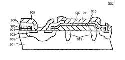
- FIG. 33 is a cross-sectional view of a conventional third semiconductor device 900.
- the conventional third semiconductor device 900 includes an active element portion and a gate pad portion defined in a semiconductor substrate in which an n + drain layer (not shown) and an n ⁇ drift layer 901 are stacked.
- a semiconductor device is provided.
- the active element section includes an n + drain layer (not shown), an n ⁇ drift layer 901, a p base region 902 formed on the surface of the n ⁇ drift layer 901, p
- a gate electrode provided on the n + source region 903 formed on the surface of the base region 902 and a p base region 902 sandwiched between the n + source region 903 and the n ⁇ drift layer 901 with a gate insulating film 904 interposed therebetween.
- 905 and the gate electrode 905 include a source electrode 908 provided in contact with the surfaces of the n + source region 903 and the p base region 902 in a state where the gate electrode 905 is insulated through the interlayer insulating film 906.
- the gate pad portion includes an n + drain layer (not shown), an n ⁇ drift layer 901, and a gate pad portion on the n ⁇ drift layer 901 via a field insulating layer 910.
- the conventional third semiconductor device 900 has a higher breakdown resistance at the time of switch-off than the conventional semiconductor device (the conventional semiconductor device 800 or the semiconductor device described in FIG. 3 of JP-A-5-167070).
- the capacitance of the parasitic diode under the gate pad is reduced.
- the value of the resistor R3 formed in the central portion of the gate pad portion is small. Therefore, in the conventional third semiconductor device 900, the gate oscillation phenomenon at the time of switch-off cannot be suppressed as in the present invention.
- a p-well layer 919 is formed in a ring shape below the gate pad portion, that is, a p-well layer 919 is formed in the central portion of the gate pad portion. Because of the absence (see FIG. 5B described later), there is a problem that the effect of stabilizing the expansion of the depletion layer under the gate pad is reduced during reverse bias.
- the semiconductor device of the present invention on the surface of the drift layer, the second conductivity type impurity diffusion region electrically connected to the first electrode layer, the second conductivity type impurity non-diffusion region, Since the gate oscillation suppressing structure is formed alternately, such a problem that the conventional third semiconductor device 900 has does not occur.
- the p well layer 919 formed below the gate pad portion is not connected to the source electrode, the p well layer 919 is reversed in the region where the p well layer 919 is not formed. Since the depletion layer does not expand at the time of bias, the electric field strength does not decrease and the breakdown voltage decreases.
- the semiconductor device of the present invention on the surface of the drift layer, the second conductivity type impurity diffusion region electrically connected to the first electrode layer, the second conductivity type impurity non-diffusion region, Such a problem does not occur because the gate oscillation suppression structure is formed alternately.
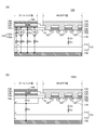
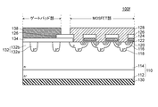
- FIG. 1 is a diagram for explaining a semiconductor device 100 according to a first embodiment.
- 1 is a diagram for explaining a semiconductor device 100 according to a first embodiment.
- FIG. 6 is a diagram for explaining the effect of the semiconductor device 100 according to the first embodiment.
- FIG. 6 is a diagram for explaining the effect of the semiconductor device 100 according to the first embodiment.
- FIG. 6 is a diagram for explaining the effect of the semiconductor device 100 according to the first embodiment.
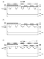
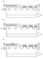
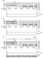
- FIG. 6 is a view for explaining the method for manufacturing the semiconductor device according to the first embodiment.
- FIG. 6 is a view for explaining the method for manufacturing the semiconductor device according to the first embodiment.
- FIG. 6 is a view for explaining the method for manufacturing the semiconductor device according to the first embodiment.
- FIG. 6 is a view for explaining the method for manufacturing the semiconductor device according to the first embodiment.
- FIG. 6 is a view for explaining the method for manufacturing the semiconductor device according to the first embodiment. It is a figure shown in order to demonstrate the semiconductor device 100a which concerns on Embodiment 2. FIG. It is a figure shown in order to demonstrate the semiconductor device 100b which concerns on Embodiment 3. FIG. It is a figure shown in order to demonstrate the semiconductor device 100c which concerns on Embodiment 4. FIG. It is a figure shown in order to demonstrate the semiconductor device 100d which concerns on Embodiment 5. FIG. It is sectional drawing of the semiconductor device 100e which concerns on Embodiment 6. FIG. It is sectional drawing of the semiconductor device 100f which concerns on Embodiment 7. FIG. It is a figure shown in order to demonstrate the semiconductor device 100g which concerns on Embodiment 8. FIG.
- FIG. 14 is a cross-sectional view of a semiconductor device 200 according to Embodiment 13.
- FIG. 20 is a cross-sectional view of a semiconductor device 200b according to Embodiment 15.
- FIG. 20 is a cross-sectional view of a semiconductor device 200b according to Embodiment 15.
- FIG. 16 is a cross-sectional view of a semiconductor device 300 according to a sixteenth embodiment. It is a figure shown in order to demonstrate the semiconductor device 100l based on Embodiment 17.
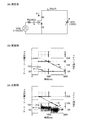
- FIG. It is sectional drawing of the semiconductor devices 100i and 100C used for Test Example 1 and 2.
- FIG. It is a figure shown in order to demonstrate the evaluation result of the test example 1.
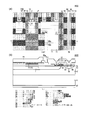
- FIG. It is a figure shown in order to demonstrate the evaluation method and evaluation result in Test Example 2.
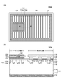
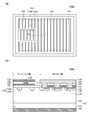
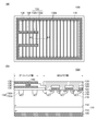
- FIG. 1A is a plan view of the semiconductor device 100
- FIG. 1B is a cross-sectional view taken along line A1-A1 of FIG. 2A is a plan view of the semiconductor device 100
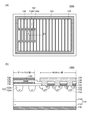
- FIG. 2B is a cross-sectional view taken along line A2-A2 of FIG. 2A.
- FIG. 1A the contour lines of the p + -type overhanging diffusion region 118, the p + -type diffusion regions 132a and 162, the p-type impurity non-diffusion region 132b, the gate oscillation suppressing structure 132, and the source electrode layer 128 (one point) Only a chain line) is shown.
- FIG. 2A only the contour lines (dashed lines) of the polysilicon layer 136 and the source electrode layer 128 are shown.
- FIG. 1A the p + type overhanging diffusion region 118 and the p + type diffusion regions 132a and 162 are shown in a dot pattern
- FIG. 1B the p + type overhanging diffusion region 118 and the p + type diffusion are illustrated.
- the region 132a is indicated by a white pattern.
- reference numeral 130 denotes a drain electrode layer.
- the semiconductor device 100 includes a MOSFET portion (defined by a semiconductor substrate 110 in which an n + -type low-resistance semiconductor layer 112 and an n ⁇ -type drift layer 114 are stacked).
- This is a semiconductor device (power MOSFET) provided with a gate pad portion and a gate finger portion.
- the MOSFET portion includes a low-resistance semiconductor layer 112, a drift layer 114 formed on the low-resistance semiconductor layer 112, and a p-type base region formed on the surface of the drift layer 114.
- the gate pad portion includes a low-resistance semiconductor layer 112, a drift layer 114 formed on the low-resistance semiconductor layer 112, and a drift insulating layer 114 on the drift layer 114 via a field insulating layer 134.
- a gate oscillation suppressing structure 132 in which 132a corresponding to a conductive impurity diffusion region) 132a and n ⁇ type p-type impurity non-diffusion regions (corresponding to the second conductivity type impurity non-diffusion region of the present invention) 132b are alternately formed; Is provided.
- the p + type diffusion region 132a is electrically connected to the source electrode layer 128 through a p + type diffusion region 162 and a p + type overhanging diffusion region 118 described later.
- the p + -type diffusion region, the p-type diffusion region, and the p ⁇ -type diffusion region correspond to the second conductivity type impurity diffusion region, and the p-type impurity non-existence region.
- the diffusion region corresponds to the second conductivity type impurity non-diffusion region.
- the gate finger portion includes the low resistance semiconductor layer 112, the drift layer 114 formed on the low resistance semiconductor layer 112, and the drift layer 114 via the field insulating layer 134.
- a polysilicon layer 136 formed over the entire surface of the gate finger portion and a p + type diffusion region (second conductivity type impurity diffusion region) 162 formed over the entire surface of the drift layer 114 are provided.
- the p + type diffusion region 162 is electrically connected to the source electrode layer 128 through the p + type overhanging diffusion region 118.
- an interlayer insulating layer 126 is formed on the polysilicon layer 136 in the gate pad portion, and the gate pad is formed on the interlayer insulating layer 126.
- An electrode layer 138 is formed. The polysilicon layer 136 and the gate pad electrode layer 138 are electrically connected through a through hole 140 provided in the interlayer insulating layer 126.
- the interlayer insulating layer 126 is formed on the polysilicon layer 136 in the gate finger portion, and the gate finger is formed on the interlayer insulating layer 126.
- a wiring layer 142 is formed. The polysilicon layer 136 and the gate finger wiring layer 142 are electrically connected through a through hole 140 provided in the interlayer insulating layer 126.
- the polysilicon layer 136 is electrically connected to the gate electrode layer 124 via a gate finger portion that connects the gate pad electrode layer 138 and the gate electrode layer 124. In addition, there is no portion that is directly connected to the gate electrode layer 124 without going through the gate finger portion.
- the p-type impurity non-diffusion region 132b is formed in a stripe shape in the gate pad portion.
- the p + -type diffusion region 132a is formed in a stripe shape in which both ends are connected so as to surround the p-type impurity non-diffusion region 132b.
- the cell adjacent to the gate pad portion has a structure in which the source region 120 on the gate pad portion side is deleted (refer to a portion indicated by reference numeral B in FIG. 5 described later).
- the MOSFET section further includes a p + type protruding diffusion region 118 formed so as to protrude downward (in the deep direction) from the base region 116.
- P + -type diffusion region 132a of the gate pad part is a MOSFET of the p + -type flared diffusion region 118 and the gate finger portion p + -type diffusion region 162 and the same process, and the MOSFET section p + -type flared diffusion region 118 And the p + -type diffusion region 162 of the gate finger portion.
- the p + -type diffusion region 132a does not have an n-type semiconductor region inside.
- the entire gate pad portion having an area occupied by the portion of the polysilicon layer 136 as the conductor layer facing the drift layer 114 through the field insulating layer 134 in the gate pad portion.
- the ratio to the area is larger than the ratio of the area occupied by the portion where the gate electrode layer 124 faces the drift layer 114 via the gate insulating layer 122 in the MOSFET portion to the area of the entire MOSFET portion.
- the thickness of the low resistance semiconductor layer 112 is 100 ⁇ m to 400 ⁇ m, and the impurity concentration of the low resistance semiconductor layer 112 is 1 ⁇ 10 19 cm ⁇ 3 to 1 ⁇ 10 20 cm ⁇ 3 .
- the thickness of the drift layer 114 is 5 ⁇ m to 50 ⁇ m, and the impurity concentration of the drift layer 114 is 1 ⁇ 10 14 cm ⁇ 3 to 1 ⁇ 10 16 cm ⁇ 3 .
- the depth of the base region 116 is 2 ⁇ m to 2.5 ⁇ m, and the impurity concentration of the base region 116 is 5 ⁇ 10 16 cm ⁇ 3 to 1 ⁇ 10 18 cm ⁇ 3 .
- the depth of the source region 120 is 0.2 ⁇ m to 0.4 ⁇ m, and the impurity concentration of the source region 120 is 5 ⁇ 10 19 cm ⁇ 3 to 2 ⁇ 10 20 cm ⁇ 3 .
- the depth of the p + -type overhanging diffusion region 118 is 2.4 ⁇ m to 8.0 ⁇ m, and the impurity concentration of the p + type overhanging diffusion region 118 is 1 ⁇ 10 17 cm ⁇ 3 to 3 ⁇ 10 18 cm ⁇ 3 .
- the depth of the p + -type diffusion region 132a is 2.4 ⁇ m to 8.0 ⁇ m, and the impurity concentration of the p + -type diffusion region 132a is 1 ⁇ 10 17 cm ⁇ 3 to 3 ⁇ 10 18 cm ⁇ 3 .
- the base region 116, the p + -type overhanging diffusion region 118, the gate electrode layer 124, and the p + -type diffusion region 132a are formed in a stripe shape.
- the formation pitch of the base region 116, the p + -type overhanging diffusion region 118, and the gate electrode layer 124 is, for example, 15 ⁇ m
- the formation pitch of the p + -type diffusion region 132a is, for example, 15 ⁇ m.
- the stripe width of the base region 116 is, for example, 9 ⁇ m
- the stripe width of the p + type overhanging diffusion region 118 is, for example, 3.75 ⁇ m
- the stripe width of the gate electrode layer 124 is, for example, 6 ⁇ m.
- the stripe width of the p + -type diffusion region 132a is, for example, 8 ⁇ m.
- the gate insulating layer 122 is made of a silicon dioxide film having a thickness of, for example, 100 nm formed by a thermal oxidation method.
- the field insulating layer 134 is formed of a silicon dioxide film having a thickness of, for example, 450 nm formed by a thermal oxidation method.
- the interlayer insulating layer 126 is made of a PSG film having a thickness of 1000 nm formed by a CVD method.
- the gate electrode layer 124 is formed of a low resistance polysilicon film having a thickness of, for example, 500 nm formed by a CVD method and an ion implantation method.
- the polysilicon layer 136 is formed of a low resistance polysilicon film having a thickness of, for example, 500 nm formed by a CVD method and an ion implantation method.
- the gate electrode layer 124 and the polysilicon layer 136 are formed by the same process.
- the source electrode layer 128 is made of an aluminum film having a thickness of 4 ⁇ m, for example, formed by sputtering.
- the gate pad electrode layer 138 and the gate finger wiring layer 142 are made of an aluminum film having a thickness of, for example, 4 ⁇ m formed by sputtering.
- the source electrode layer 128, the gate pad electrode layer 138, and the gate finger wiring layer 142 are formed in the same process.
- the drain electrode layer 130 is formed of a multilayer metal film such as Ti—Ni—Au, and has a thickness of, for example, 0.5 ⁇ m over the entire multilayer metal film.
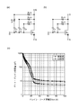
- FIGS. 3 to 5 are diagrams for explaining the effects of the semiconductor device 100 according to the first embodiment.
- 3A is a diagram in which parasitic capacitance and parasitic resistance are added to the cross-sectional view of the semiconductor device 100 according to the first embodiment
- FIG. 3B is a cross-sectional view of the semiconductor device 100A according to the first comparative example. It is the figure which added and parasitic resistance.
- the semiconductor device 100A according to Comparative Example 1 basically corresponds to the conventional semiconductor device 800.
- FIG. 4 (a) to 4 (d) are diagrams showing how the depletion layer d expands at the time of reverse bias, and FIG. 4 (a) shows the expansion of the depletion layer d when no reverse bias voltage is applied.
- 4 (b) is a diagram showing how the depletion layer d expands when a low reverse bias voltage is applied, and FIG. 4 (c) shows a moderate reverse bias voltage.
- FIG. 4D is a diagram illustrating a state in which the depletion layer d expands when a high reverse bias voltage is applied.
- the low-resistance semiconductor layer 112, the drain electrode layer 130, the interlayer insulating layer 126, and the source electrode layer 128 are not shown.
- FIG. 5A is a diagram in which parasitic capacitance and parasitic resistance are added to the cross-sectional view of the semiconductor device 100 according to the first embodiment
- FIG. 5B is a cross-sectional view of the semiconductor device 100B according to the comparative example 2. It is the figure which added and parasitic resistance.
- the semiconductor device 100B according to the comparative example 2 basically corresponds to the third semiconductor device 900 in the related art.
- 5 (a) and 5 (b) show the MOSFET portion smaller than that in FIGS. 3 (a) and 3 (b) and the gate pad portion larger.
- the gate-drain capacitance, the capacitance of the capacitor C 0 that is formed in the MOSFET portion, the capacitor C is formed in the gate pad portion 1 is added (see FIG. 3B).
- the capacitor C 1 formed in the gate pad portion includes ““ the conductor layer (polysilicon layer 136) as one electrode ”,“ the field insulating layer 134 and p + -type diffusion region 158 as a dielectric ”, and It has a structure in which “n ⁇ drift layer 114 as the other electrode” is stacked (see FIG. 3B).
- the gate-drain capacitance the capacitance of the capacitor C 0 that is formed in the MOSFET section
- the value is obtained by adding the capacitances of the capacitors C 2 and C 3 .
- the capacitor C 2 is a capacitor formed in the region where the p + -type diffusion region 132a is formed on the surface of the drift layer 114, and ““ the conductor layer (polysilicon layer 136) as one electrode ”. ”,“ Field insulating layer 134 as dielectric and p + -type diffusion region 132a ”and“ drift layer 114 as the other electrode ””.
- the capacitor C 3 is a capacitor with a p-type impurity is formed in a region that has not been diffused (p-type impurity-doped diffusion regions 132b) at the surface of the drift layer 114, "" whereas the conductor layer as an electrode (
- the capacitor is composed of “polysilicon layer 136)”, “field insulating layer 134 as a dielectric” and “drift layer 114 as the other electrode”.
- the field insulating layer 134 is usually formed much thinner than the p + type diffusion region 132a (field insulating layer 134: 200 nm to 500 nm, p + type diffusion region). 132a: 2.4 ⁇ m to 8.0 ⁇ m), among the capacitors C 1 , C 2 , and C 3 , the capacitance of the capacitor C 3 becomes extremely large. As a result, the gate-drain capacitance of the semiconductor device 100 according to the first embodiment Crss becomes larger than the gate-drain capacitance Crss of the conventional semiconductor device 800 (or the semiconductor device 100A according to Comparative Example 1).
- a narrow region (p-type impurity non-diffusion region 132b) sandwiched between adjacent p + -type diffusion regions 132a on the surface of the drift layer 114 serves as a current path ( 3a), and the current path becomes narrower and longer as a result of the depletion layer spreading from the p + -type diffusion region 132a to the drift layer side when the switch is turned off, and Eventually, depletion occurs, so that a resistor having a relatively large resistance value (see the resistor R3 in FIG. 3A) is formed in the narrow region described above.
- the semiconductor device 100 since a large capacitance and resistance can be formed between the gate and the drain, when the switch is turned off without adding a capacitance and a resistance between the gate and the drain. It becomes possible to suppress the gate oscillation phenomenon in.
- the p + -type diffusion region 132a electrically connected to the source electrode layer 128 and the p-type impurity are formed on the surface of the drift layer 114. Since the gate oscillation suppressing structure in which the non-diffusion regions 132b are alternately formed is provided, as shown in FIGS. 4 (a) to 4 (d), the depletion layers extend in the lateral direction and contact each other at the time of reverse bias. However, by extending toward the low-resistance semiconductor layer 112 over the entire surface of the gate pad portion, a high-breakdown-voltage semiconductor device can be configured as in the case of the conventional semiconductor device 800.
- the p-well layer 919 (132c) is formed in a ring shape below the gate pad portion.
- the conventional third semiconductor device 900 (or the semiconductor device 100B according to the comparative example 2) is a conventional semiconductor device (the conventional semiconductor device 800 or the semiconductor device shown in FIG. 3 of Japanese Patent Laid-Open No. 5-167070). ), The capacitance of the parasitic diode under the gate pad portion is reduced in order to increase the breakdown tolerance when the switch is turned off. Further, in the conventional third semiconductor device 900 (or the semiconductor device 100B according to the comparative example 2), the p-well layer 919 (132c) is not formed in the central portion of the gate pad portion. The value of the resistor R3 formed in the center portion is small. For this reason, in the conventional third semiconductor device 900, unlike the semiconductor device 100 according to the first embodiment, the gate oscillation phenomenon at the time of switching off cannot be suppressed.
- the p-well layer 919 (132c) is formed in a ring shape below the gate pad portion, that is, the gate pad. Since the p-well layer 919 (132c) is not formed in the central portion of the portion (see FIGS. 33 and 5B), the effect of stabilizing the expansion of the depletion layer under the gate pad portion during reverse biasing. There is also a problem that becomes smaller.
- the p-well layer 919 (132c) formed under the gate pad portion is not connected to the source electrode.
- the depletion layer does not expand at the time of reverse bias, so the electric field strength does not decrease and the breakdown voltage decreases.
- the interlayer insulating layer 126 is formed on the polysilicon layer 136 as the conductor layer, and the gate pad electrode layer 138 is formed on the interlayer insulating layer 126. Therefore, the multilayer structure composed of the polysilicon layer 136, the interlayer insulating layer 126, and the gate pad electrode layer 138 comes to act as a buffer when connecting the external terminal to the gate pad electrode layer 138. A highly reliable semiconductor device can be configured.
- the polysilicon layer 136 is interposed via the gate finger portion that connects the gate pad electrode layer 138 and the gate electrode layer 124.
- the gate pad electrode layer 138 is not connected to the gate electrode layer 124 without passing through the gate finger portion, so that the gate pad electrode layer 138 is not connected to the gate electrode layer 124.
- the distance between the gate pad electrode layer 138 and the gate electrode layer 124 is longer than in the case of the semiconductor device 100B according to Comparative Example 2 that is directly connected to the gate 124 (see the portion indicated by the symbol C in FIG. 5B). This also makes it possible to suppress the gate oscillation phenomenon.
- the semiconductor device 100 according to the first embodiment has a structure in which the source region 120 on the gate pad portion side is deleted in the cell adjacent to the gate pad portion (see FIGS. 5A and 5B). (See the portion indicated by the symbol B.) As described above, the semiconductor device 100 according to the first embodiment has a structure in which the source region 120 that is closest to the gate pad portion and is most likely to cause the gate oscillation phenomenon is deleted. It becomes possible to suppress.
- the p + type diffusion region 132a of the gate pad part is formed in the same process as the p + type overhanging diffusion region 118 of the MOSFET part, No extra process is performed to form the p + -type diffusion region 132a in the portion.
- p + -type diffusion region 132a of the gate pad portion and is formed to be continuous with the p + -type flared diffusion region 118 of the MOSFET portion, p + -type diffusion region 132a of the gate pad portion MOSFET portion the p + -type overhang now given the same potential as the potential of the diffusion region 118, so that, at the time of reverse bias that the depletion layer in the drift layer 114 is extended toward the drain layer, a semiconductor device of high breakdown voltage It can be configured.
- the p-type impurity non-diffusion region 132b is formed in a stripe shape, and the p + -type diffusion region 132a is the p-type impurity non-diffusion region. Since it is formed in a stripe shape having both ends connected so as to surround 132b, the p-type impurity non-diffusion region 132b is easily depleted during reverse bias, and this also constitutes a high breakdown voltage semiconductor device. It becomes possible.
- the semiconductor device 100 since the p + -type diffusion region 132a does not have an n-type semiconductor region, the reach-through phenomenon does not occur and a high breakdown voltage can be secured. It is done.
- the field insulating layer 134 that is required to have high insulation due to its large area is thicker than the gate insulating layer 122, and therefore, the reliability is excellent in insulation.
- a high semiconductor device can be configured.
- the entire gate pad portion has an area occupied by the portion of the gate pad portion where the polysilicon layer 136 as the conductor layer faces the drift layer 114 via the field insulating layer 134. Is larger than the ratio of the area occupied by the portion where the gate electrode layer 124 faces the drift layer 114 through the gate insulating layer 122 in the MOSFET portion to the area of the entire MOSFET portion. Crss can be effectively increased.
- Manufacturing method of semiconductor device according to embodiment 1 The semiconductor device 100 according to the first embodiment can be manufactured by a manufacturing method (a manufacturing method of a semiconductor device according to the first embodiment) having the following manufacturing process.
- 6 to 10 are views for explaining the method of manufacturing the semiconductor device according to the first embodiment.
- FIG. 6A to FIG. 10C show each step.
- a semiconductor substrate 110 is prepared in which a silicon layer constituting the drift layer 114 is formed on the silicon substrate constituting the low resistance semiconductor layer 112 by an epitaxial growth method.
- the thickness of the low-resistance semiconductor layer 112 is, for example, 100 ⁇ m to 400 ⁇ m, and the impurity concentration of the low-resistance semiconductor layer 112 is 1 ⁇ 10 19 cm ⁇ 3 to 1 ⁇ 10 20 cm ⁇ 3 .
- the thickness of the drift layer 114 is 5 ⁇ m to 50 ⁇ m, and the impurity concentration of the drift layer 114 is 1 ⁇ 10 14 cm ⁇ 3 to 1 ⁇ 10 16 cm ⁇ 3 .
- a heat treatment is performed on the semiconductor substrate 110 in an oxygen gas-containing atmosphere to form the p + -type overhanging diffusion region 118 and the p + -type diffusion region 132a (see FIG. 6B).
- the formation depth of the p + type overhang diffusion region 118 and the p + type diffusion region 132a is 2.4 ⁇ m to 8.0 ⁇ m, and the impurity concentration of the p + type overhang diffusion region 118 and the p + type diffusion region 132a is 1 ⁇ 10 17. cm ⁇ 3 to 3 ⁇ 10 18 cm ⁇ 3 .
- the p-type impurity non-diffusion region 132b is formed in the portion where the p-type impurity is not diffused on the surface of the drift layer 114. Further, the surface of the drift layer 114 is thermally oxidized to form the field insulating layer 134.
- the thickness of the field insulating layer 134 is 450 nm, for example.
- the field insulating layer 134 is etched to expose the drift layer 114 in the MOSFET portion. (See FIG. 6C.) Thereafter, the surface of the drift layer 114 is thermally oxidized by performing a heat treatment of the semiconductor substrate 110 in an oxygen gas-containing atmosphere to form a gate insulating layer 122 in the MOSFET portion (see FIG. 7A).
- the thickness of the gate insulating layer 122 is, for example, 100 nm.
- a low resistance polysilicon layer 123 is formed on the surface of the field insulating layer 134 and the gate insulating layer 122 by a CVD method (see FIG. 7B).
- the thickness of the polysilicon layer 123 is, for example, 500 nm.
- a mask (not shown) is formed in a region corresponding to the polysilicon layer 136 and a region corresponding to the gate electrode layer 124, and then the polysilicon layer 123 is etched to form the gate electrode layer 124 in the MOSFET portion.
- a polysilicon layer 136 is formed in the gate pad portion (see FIG. 7C).
- p-type impurities for example, boron ions
- p-type impurities for example, boron ions
- a p-type impurity is introduced into a region corresponding to the base region 116 on the surface of the drift layer 114 (see FIG. 8A).
- heat treatment of the semiconductor substrate 110 is performed to perform activation annealing of p-type impurities, thereby forming the base region 116 (see FIG. 8B).
- the depth of the base region 116 is 2 ⁇ m to 2.5 ⁇ m, and the impurity concentration of the base region 116 is 5 ⁇ 10 16 cm ⁇ 3 to 1 ⁇ 10 18 cm ⁇ 3 .
- a mask M2 is formed in a region on the gate insulating layer 122 excluding the region where the source region 120 is formed, and the gate is formed using the mask M2, the gate electrode layer 124, and the field insulating layer 134 as a mask.
- an n-type impurity for example, phosphorus ions
- the n-type impurity is introduced into a region corresponding to the source region 120 on the surface of the drift layer 114 (See FIG. 8 (c)).
- the depth of the source region 120 is 0.2 ⁇ m to 0.4 ⁇ m, and the impurity concentration of the source region 120 is 5 ⁇ 10 19 cm ⁇ 3 to 2 ⁇ 10 20 cm ⁇ 3 .
- a predetermined region of the metal layer 127 is removed by etching, and the metal layer 127 is separated into the source electrode layer 128 and the gate pad electrode layer 138, whereby the source electrode layer 128 and the gate pad electrode layer 138 are formed.
- the thicknesses of the source electrode layer 128 and the gate pad electrode layer 138 are, for example, 4 ⁇ m.
- a metal film made of a multilayer metal film such as Ti—Ni—Au is formed on the surface of the semiconductor substrate 110 on the second main surface side (surface of the low resistance semiconductor layer 112) to form the drain electrode layer 130 (FIG. 10 (c)).
- the thickness of the drain electrode layer 130 is, for example, 0.5 ⁇ m for the entire multilayer metal film.
- the semiconductor device 100 according to the first embodiment can be manufactured.
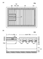
- FIG. 11 is a diagram for explaining the semiconductor device 100a according to the second embodiment.
- FIG. 11A is a plan view of the semiconductor device 100a
- FIG. 11B is a cross-sectional view taken along line A1-A1 of FIG.
- FIG. 12 is a diagram for explaining the semiconductor device 100b according to the third embodiment.
- FIG. 12A is a plan view of the semiconductor device 100b
- FIG. 12B is a cross-sectional view taken along line A1-A1 of FIG.
- FIG. 13 is a diagram for explaining the semiconductor device 100c according to the fourth embodiment.
- FIG. 13A is a plan view of the semiconductor device 100c
- FIG. 13B is a cross-sectional view taken along line A1-A1 of FIG. FIG.
- FIG. 14 is a diagram for explaining the semiconductor device 100d according to the fifth embodiment.
- 14A is a plan view of the semiconductor device 100d
- FIG. 14B is a cross-sectional view taken along line A1-A1 of FIG.
- reference numeral 130 denotes a drain electrode layer.
- 11A, 12A, 13A, and 14A the p + type overhanging diffusion region 118 and the p + type diffusion regions 132a and 162 are shown in a dot pattern.
- 11 (b), FIG. 12 (b), FIG. 13 (b), and FIG. 14 (b) the p + -type overhanging diffusion region 118 and the p + -type diffusion region 132a are shown in white.
- the semiconductor devices 100a to 100d according to the second to fifth embodiments basically have the same configuration as the semiconductor device 100 according to the first embodiment, but the planar structure of the gate oscillation suppressing structure 132 is the semiconductor device according to the first embodiment. Different from 100. That is, in the semiconductor device 100a according to the second embodiment, as shown in FIG. 11, the stripe pitch of the p + -type diffusion region 132a in the gate oscillation suppressing structure 132 is narrower than that in the semiconductor device 100 according to the first embodiment. Further, in the semiconductor device 100b according to the third embodiment, as shown in FIG. 12, the width of the p + -type diffusion region 132a in the gate oscillation suppressing structure 132 is wider than that in the semiconductor device 100 according to the first embodiment.
- the stripe orientation of the p + -type diffusion region 132a in the gate oscillation suppressing structure 132 is different from that in the semiconductor device 100 according to the first embodiment.
- the p + -type overhanging diffusion region 118 is orthogonal to the stripe direction.
- the shape of the p-type impurity non-diffusion region 132b in the gate oscillation suppressing structure 132 is different from that in the semiconductor device 100 according to the first embodiment.
- Island shape That is, the shape of the p + -type diffusion region 132a is a lattice shape.
- FIG. 15 is a cross-sectional view of a semiconductor device 100e according to the sixth embodiment.
- FIG. 16 is a cross-sectional view of a semiconductor device 100f according to the seventh embodiment.
- the semiconductor devices 100e and 100f according to the sixth and seventh embodiments basically have the same configuration as the semiconductor device 100 according to the first embodiment, but the semiconductor device 100 according to the first embodiment has an electrode stack structure in a gate pad portion. It is different from the case of. That is, in the semiconductor device 100e according to the sixth embodiment, as shown in FIG. 15, the gate pad electrode layer 138 is directly formed on the substantially entire surface of the polysilicon layer 136 as a conductor layer without the interlayer insulating layer 126 interposed therebetween. Is formed. In the semiconductor device 100f according to the seventh embodiment, as shown in FIG. 16, the gate pad electrode layer 138 as a conductor layer is formed directly on the entire surface of the field insulating layer 134 without a polysilicon layer. Has been.
- FIG. 17 is a view for explaining the semiconductor device 100g according to the eighth embodiment.
- 17A is a plan view of the semiconductor device 100g
- FIG. 17B is a cross-sectional view taken along line A1-A1 of FIG.
- reference numeral 130 denotes a drain electrode layer.
- the semiconductor device 100g according to the eighth embodiment has basically the same configuration as that of the semiconductor device 100 according to the first embodiment, but the step of forming the second conductivity type impurity diffusion region is the same as that of the semiconductor device 100 according to the first embodiment. Different from the case. That is, in the semiconductor device 100g according to the eighth embodiment, as shown in FIG. 17, the p + type contact region 144 is formed in the MOSFET portion instead of the p + type overhanging diffusion region, and the p type diffusion region 133a is , P + -type overhanging diffusion region, not the base region 116 but formed in the same process.
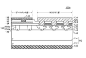
- FIG. 18 is a cross-sectional view of a semiconductor device 100h according to the ninth embodiment.
- FIG. 19 is a cross-sectional view of the semiconductor device 100 i according to the tenth embodiment.
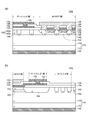
- FIG. 20 is a diagram for explaining the semiconductor device 100j according to the eleventh embodiment.
- 20A is a cross-sectional view of the gate pad portion and the MOSFET portion in the semiconductor device 100j
- FIG. 20B is a cross-sectional view of the MOSFET portion, the gate finger portion, and the guard ring portion in the semiconductor device 100j.
- reference numeral 150b denotes a p-type impurity non-diffusion region (corresponding to the second conductivity type impurity non-diffusion region of the present invention), and reference numeral 150 denotes a gate oscillation suppressing structure.
- the semiconductor devices 100h to 100j according to the ninth to eleventh embodiments basically have the same configuration as that of the semiconductor device 100 according to the first embodiment, but include p + containing a p-type impurity at a concentration higher than that of the base region 116.
- the embodiment 1 includes a p ⁇ type diffusion region (corresponding to the second conductivity type impurity diffusion region of the present invention) 150a containing a p type impurity having a lower concentration than the base region 116 instead of the type diffusion region 132a. This is different from the case of the semiconductor device 100. That is, in the semiconductor devices 100h to 100j according to the ninth to eleventh embodiments, as shown in FIGS.
- the semiconductor devices 100h to 100j are formed shallower than the base region 116 between the adjacent base regions 116, and more than the drift layer 114.
- An n-type reference concentration semiconductor layer 146 containing an n-type impurity having a higher concentration and a lower concentration than the source region 120 is provided in the MOSFET portion.
- a p + -type overhanging diffusion region 118 containing a p-type impurity having a higher concentration than the base region 116 a p ⁇ type overhanging diffusion region 148 containing a p-type impurity having a lower concentration than the base region 116 is replaced with a MOSFET portion.
- a p ⁇ -type diffusion region 150a containing a p-type impurity at a lower concentration than the base region 116 is used instead of the p + -type diffusion region 132a containing a p-type impurity at a higher concentration than the base region 116.
- the technique for forming the n-type reference concentration semiconductor layer 146 and the p ⁇ -type overhanging diffusion region 148 in the MOSFET part is a technique developed by the present applicant, and is described in detail in Japanese Patent Application Laid-Open No. 2011-228643. .
- the n-type reference concentration semiconductor layer 146 extends to the gate pad portion (see FIG. 18).
- the n-type reference concentration semiconductor layer 146 is formed only in the MOSFET portion (see FIG. 19).
- the surface of the n-type reference concentration semiconductor layer 146 is formed shallower than the n-type reference concentration semiconductor layer 146 and has a higher concentration than the n-type reference concentration semiconductor layer 146.
- an n + -type semiconductor layer 152 containing an n-type impurity at a lower concentration than the source region 120 is provided in the MOSFET portion (see FIG. 20).
- the p ⁇ type diffusion region 150a of the gate pad portion is in the same process as the p ⁇ type overhanging diffusion region 148 of the MOSFET portion, and the p ⁇ type diffusion region 148 of the MOSFET portion. - is formed so as to be continuous with the type flared diffusion region 148 (see FIGS. 18 to 20.).
- the semiconductor device 100i according to the tenth embodiment can be manufactured by the following semiconductor device manufacturing method.
- FIG. 21 is a view for explaining the method for manufacturing the semiconductor device according to the tenth embodiment.
- 21A to 21C are process diagrams.
- the manufacturing method of the semiconductor device according to the tenth embodiment basically includes the same steps as the manufacturing method of the semiconductor device according to the first embodiment, except that the n-type reference concentration semiconductor layer 146, the p ⁇ -type overhanging diffusion region 148, and The content of the step of forming the p ⁇ -type diffusion region 150a is different from that in the method for manufacturing the semiconductor device according to the first embodiment. Therefore, a method for manufacturing the semiconductor device according to the tenth embodiment will be described focusing on the steps of forming the n-type reference concentration semiconductor layer 146, the p ⁇ -type overhanging diffusion region 148, and the p ⁇ -type diffusion region 150a.
- n-type Reference Concentration Semiconductor Layer Corresponding to n-type reference concentration semiconductor layer 146 after performing “preparation of semiconductor substrate (process)” in the same manner as in the method of manufacturing a semiconductor device according to the first embodiment.
- a silicon dioxide thin film M3 having an opening in a region to be formed is formed, and an n-type impurity (for example, phosphorus ions) is implanted into the surface of the drift layer 114 through the silicon dioxide thin film M3 by an ion implantation method.
- An n-type impurity is introduced into a region corresponding to the n-type reference concentration semiconductor layer 146 (see FIG. 21A).
- the semiconductor substrate 110 is heat-treated in an oxygen gas-containing atmosphere, thereby forming the n-type reference concentration semiconductor layer 146, the p ⁇ -type overhanging diffusion region 148, and the p ⁇ -type diffusion region 150a (FIG. 21C). reference.).
- the formation depth of the p ⁇ -type overhanging diffusion region 148 and the p ⁇ -type diffusion region 150a is 6.0 ⁇ m to 8.0 ⁇ m
- the impurity concentration of the p ⁇ -type overhanging diffusion region 148 and the p ⁇ -type diffusion region 150a is 1 ⁇ 10 17. cm ⁇ 3 to 3 ⁇ 10 18 cm ⁇ 3 .
- the surface of the drift layer 114 is thermally oxidized to form the field insulating layer 134.
- the thickness of the field insulating layer 134 is 450 nm, for example.
- the surface of the drift layer 114 is also formed in the gate pad portion by the ion implantation method when the “n-type reference concentration semiconductor layer formation” step is performed.
- An n-type impurity (for example, phosphorus ion) is implanted into the first electrode.
- the n + type semiconductor only the region for forming the layer 152 by implanting an n-type impurity (e.g., phosphorus ions) in the surface of the drift layer 114 by ion implantation, the region for forming the n + -type semiconductor layer 152 in the surface of the drift layer 114 n Type impurities are introduced. Then, the n + -type semiconductor layer 152 is formed by performing heat treatment of the semiconductor substrate 110 to perform activation annealing of n-type impurities.
- an n-type impurity e.g., phosphorus ions
- FIG. 22 is a view for explaining the semiconductor device 100k according to the twelfth embodiment.
- 22A is a cross-sectional view of the gate pad portion and the MOSFET portion in the semiconductor device 100k
- FIG. 22B is a cross-sectional view of the MOSFET portion, the gate finger portion, and the guard ring portion in the semiconductor device 100k.
- the semiconductor device 100k according to the twelfth embodiment basically has the same configuration as that of the semiconductor device 100 according to the first embodiment, but the process of forming the p + -type semiconductor region is different from that in the semiconductor device 100 according to the first embodiment. Different. That is, in the semiconductor device 100k according to the twelfth embodiment, the p + -type contact region 144 is formed in the MOSFET portion instead of the p + -type overhanging diffusion region 118, and the p + -type diffusion region 132a in the gate pad portion becomes the MOSFET portion.
- the p + -type diffusion region 162 and the guard ring 154 are formed in the same process (see FIG. 22).
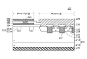
- FIG. 23 is a cross-sectional view of the semiconductor device 200 according to the thirteenth embodiment.
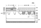
- FIG. 24 is a cross-sectional view of a semiconductor device 200a according to the fourteenth embodiment.
- FIG. 25 is a cross-sectional view of a semiconductor device 200b according to the fifteenth embodiment.
- the semiconductor devices 200 to 200b according to the thirteenth to fifteenth embodiments basically have the same configuration as the semiconductor device 100 according to the first embodiment, but the first embodiment is that the MOSFET portion has a trench structure instead of a planar structure. This is different from the case of the semiconductor device 100 according to FIG.
- the semiconductor device 200 includes a MOSFET portion and a gate pad portion defined in 210.
- the MOSFET section has a low-resistance semiconductor layer 212, a drift layer 214 formed on the low-resistance semiconductor layer 212, a p-type base region 216 formed on the surface of the drift layer 214, and a base region 216 opened.
- the gate pad portion is formed over the entire surface of the gate pad portion over the low resistance semiconductor layer 212, the drift layer 214 formed on the low resistance semiconductor layer 212, and the drift layer 214 with the field insulating layer 234 interposed therebetween.
- the second conductive type impurity diffusion region (p-type diffusion region 233a in the thirteenth embodiment, electrically connected to the source electrode layer 128 on the surface of the drift layer 214 and the polysilicon layer 236 as the conductive layer.
- the p + -type diffusion region 232a) and the second conductivity type impurity non-diffusion region p-type impurity non-diffusion region 233b in the thirteenth embodiment and p-type impurity non-diffusion in the fourteenth and fifteenth embodiments.
- the gate oscillation suppression structure in which the regions 232a) are alternately formed (the gate oscillation suppression structure 233 in the thirteenth embodiment) In modes 14 and 15, a gate oscillation suppression structure 232) is provided.
- the gate electrode layer 224 and the source region 220 are insulated by the gate insulating layer 222.
- the p-type diffusion region 233a is formed in the same process as that of the base region 216 of the MOSFET part and is continuous with the base region 216 of the MOSFET part. (See FIG. 23). Further, in the semiconductor device 200a according to the embodiment 14, the p + -type diffusion region 232a is the same as the p + -type flared diffusion region 218 of the MOSFET section process, and the p + -type flared diffusion region 218 of the MOSFET portion continuous (See FIG. 24). In the semiconductor device 200b according to the fifteenth embodiment, the p + type diffusion region 232a is formed in the same process as a guard ring (not shown) disposed at a position surrounding the MOSFET portion (see FIG. 25). .)
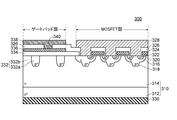
- FIG. 26 is a cross-sectional view of a semiconductor device 300 according to the sixteenth embodiment.
- the semiconductor device 300 according to the sixteenth embodiment has basically the same configuration as the semiconductor device 100 according to the first embodiment, but the semiconductor device 100 according to the first embodiment is that the semiconductor device is not a power MOSFET but an IGBT. It is different from the case of. That is, the semiconductor device 300 according to the embodiment 16, as shown in FIG. 26, an IGBT, a low-resistance semiconductor layer, and a low-resistance semiconductor layer of the p + -type instead of the n + -type low-resistance semiconductor layer .
- FIG. 27 is a view for explaining the semiconductor device 100l according to the seventeenth embodiment.
- FIG. 27A is a plan view of the semiconductor device 100l
- FIG. 27B is a cross-sectional view taken along line A1-A1 of FIG.
- reference numeral 130 denotes a drain electrode layer.
- FIG. 27A outlines of the p + -type overhanging diffusion region 118, the p + -type diffusion region 132a, the p-type impurity non-diffusion region 132b, the gate oscillation suppressing structure 132, and the source electrode layer 128 (dashed line) ) Only.
- FIG. 27A outlines of the p + -type overhanging diffusion region 118, the p + -type diffusion region 132a, the p-type impurity non-diffusion region 132b, the gate oscillation suppressing structure 132, and the source electrode layer 128 (dashed line) ) Only.
- FIG. 27A outlines of the p
- the p + -type overhanging diffusion region 118 and the p + -type diffusion region 132a are shown in a dot pattern
- FIG. 27B the p + -type overhanging diffusion region 118 and the p + -type diffusion region 132a. Is shown in white.
- the semiconductor device 100l according to the seventeenth embodiment basically has the same configuration as that of the semiconductor device 100 according to the first embodiment, but also in the gate finger portion that connects the gate pad electrode layer 138 and the gate electrode layer 124. This is different from the semiconductor device 100 according to the first embodiment in that a plurality of p + -type diffusion regions are formed apart from each other. That is, as shown in FIG. 27, the semiconductor device 100l according to the seventeenth embodiment includes a plurality of gate electrodes that connect the gate pad electrode layer 138 and the gate electrode layer 124 so as to be separated from each other on the surface of the drift layer 114. P + -type diffusion region 132a is formed.
- a field insulating layer 134 is formed on the surface of the drift layer 114 in the gate finger portion, and polysilicon is formed on the field insulating layer 134 so as to extend from the polysilicon layer 136 immediately below the gate pad electrode layer 138.
- a layer 136 is formed.
- the plurality of p + -type diffusion regions 132a may be formed in a stripe shape along the long side of the gate finger portion, or may be striped along the short side of the gate finger portion.
- the gate fingers may be formed in a lattice shape in the region of the gate finger portion, or may be formed in an island shape in the region of the gate finger portion.
- the semiconductor devices 100a to 300 according to the second to seventeenth embodiments have a partial configuration (the second to fifth embodiments: the planar structure of the gate oscillation suppressing structure 132, the sixth to seventh embodiments: the electrodes in the gate pad portion.
- Embodiments 13 to 15 MOSFET portion has a trench structure
- Embodiment 16 Semiconductor device is IGBT
- Embodiment 17 Gate finger portion also includes a plurality of p + type diffusion regions The gate pad portion is formed on the drift layer via the field insulating layer, except that the semiconductor device 100 according to the first embodiment is different from the semiconductor device 100 according to the first embodiment.
- the depletion layer expands from the second conductivity type impurity diffusion region to the drift layer side.
- the depletion layer becomes narrower, longer, and finally depleted.
- a resistor having a large resistance value is formed.
- a large capacitance and resistance can be formed between the gate and the drain. It becomes possible to suppress the gate oscillation phenomenon at the off time.
- the semiconductor devices 100h to 100j according to the ninth to eleventh embodiments and the semiconductor device 100l according to the seventeenth embodiment have the following effects.
- the source region 120 is formed between the adjacent base regions 116 to be shallower than the base region 116, and has a higher concentration than the drift layer 114. Since the n-type reference concentration semiconductor layer 146 containing an n-type impurity at a lower concentration is provided in the MOSFET portion, the semiconductor device can be miniaturized by making the interval between the base regions narrower than in the prior art. Further, even if the interval between the base regions is made narrower than before, the on-resistance of the semiconductor device is not increased. Therefore, the semiconductor devices 100h to 100j according to the ninth to eleventh embodiments can be miniaturized without increasing the on-resistance of the semiconductor device, and become a semiconductor device having good breakdown voltage characteristics. .
- the n-type reference concentration semiconductor layer 146 is formed shallower than the n-type reference concentration semiconductor layer 146 and has a higher concentration than the n-type reference concentration semiconductor layer 146.
- the n + -type semiconductor layer 152 containing n-type impurities at a lower concentration than the source region 120 is provided in the MOSFET portion, the on-resistance of the semiconductor device can be reduced, and the gate at the time of switch-off It becomes possible to more effectively suppress the oscillation phenomenon.
- the adjacent p - type diffusion region 150a narrow sandwiched region (p The resistance value of the resistance of the type impurity non-diffusion region 150b) is not too low.
- the conductor layer is also formed on the drift layer 114 via the field insulating layer 134 in the gate finger portion that connects the gate pad electrode layer 138 and the gate electrode layer 124.
- a plurality of p + -type diffusion regions 132a formed on the surface of the drift layer 114 so as to be separated from each other, the gate-drain capacitance Crss has the semiconductor device according to the first embodiment. The effect is that the gate-drain capacitance Crss of 100 is further increased.
- Test Example In configuring the semiconductor devices 100 to 300 according to Embodiments 1 to 17, the results of Test Examples 1 and 2 below were referred to.
- Test Example 1 is a test example for clarifying that the semiconductor device of the present invention has a large capacitance between the gate and the drain.
- FIG. 28 is a cross-sectional view of the semiconductor devices 100i and 100C used in Test Examples 1 and 2.
- FIG. 29 is a diagram for explaining the evaluation results of Test Example 1.
- FIG. 29A is a diagram illustrating an equivalent circuit of the semiconductor device 100i
- FIG. 29A is a diagram illustrating an equivalent circuit of the semiconductor device 100C
- FIG. 29C is a diagram illustrating the semiconductor device 100i and the semiconductor device 100C. It is a figure which shows a measurement result.
- the semiconductor devices 100i and 100C shown in FIG. 28 have slightly different structures from the semiconductor device 100 shown in FIG. 2 or the semiconductor device 100A shown in FIG. shall be represented by the same reference numerals (C 0, C 1, C 2, C 3, R 0, R 1, R 2, R 3).
- the semiconductor device has substantially the same configuration as that of the semiconductor device 100i according to the tenth embodiment, but in the gate pad portion, on the surface of the drift layer 114, the p ⁇ type diffusion region 150a and the p type impurity
- a semiconductor device including a well-shaped p ⁇ -type diffusion region 160 formed over the entire surface of the gate pad portion on the surface of the drift layer 114 instead of the gate oscillation suppressing structure 150 in which the non-diffusion regions 150b are alternately formed is a comparative example.
- the semiconductor device 100 ⁇ / b> C according to 3 is obtained.
- test Results The measurement results are shown in FIG. As a result, as can be seen from FIG. 29 (c), the semiconductor device of the present invention (semiconductor device 100i according to the example) has a larger gate-drain gap than the conventional semiconductor device (semiconductor device 100C according to comparative example 3). It became clear that it had the capacity Crss.
- Test Example 2 is a test example for clarifying that the gate oscillation phenomenon when the semiconductor device of the present invention is switched off is suppressed as compared with the conventional semiconductor device.
- FIG. 30 is a diagram for explaining an evaluation method and an evaluation result in Test Example 2.
- 30A is a diagram illustrating a measurement system used in Test Example 2
- FIG. 30B is a diagram illustrating a response waveform when the semiconductor device 100i according to the example is switched off.
- FIG. These are the figures which show the response waveform at the time of the switch-off in the semiconductor device 100C which concerns on the comparative example 3.
- the test was performed by measuring the gate-source voltage V GS and the drain current ID when the switch was turned off, using the measurement system shown in FIG.
- test results are shown in FIGS. 30 (b) and 30 (c).
- the semiconductor device of the present invention semiconductor device 100i according to the example
- the semiconductor device of the present invention is a third conventional semiconductor device 900 (semiconductor according to Comparative Example 3). It has been found that the gate oscillation phenomenon at the time of switch-off is suppressed more than in the device 100C).
- the present invention has been described with the n-type as the first conductivity type and the p-type as the second conductivity type, but the present invention is not limited to this.
- the present invention can also be applied when the p-type is the first conductivity type and the n-type is the second conductivity type.
- the conductor layer (polysilicon layer 136) is electrically connected to the gate electrode layer 124 via the gate finger portion, and the gate electrode layer 124 is not connected to the gate finger portion.
- FIG. 31 is a plan view of a semiconductor device 100m according to a modification. In FIG. 31, only the contour lines (dashed lines) of the polysilicon layer 136 and the source electrode layer 128 are shown as in the case of FIG.
- the conductor layer (polysilicon layer 136) may be laid out as shown in FIG.
- n-type reference concentration semiconductor layer 148 ... p - type overhang diffusion region, 150a, 160,164 ... p - type diffusion region, 152 ... n + type semiconductor Area, 154 ... Guard ring, 156 ... Channel stopper, 217 ... Tren H, 320 ... emitter region, 328 ... emitter electrode layer, 330 ... collector electrode layer
Landscapes
- Insulated Gate Type Field-Effect Transistor (AREA)
- Electrodes Of Semiconductors (AREA)
- Chemical & Material Sciences (AREA)
- Composite Materials (AREA)
- Semiconductor Integrated Circuits (AREA)
- Metal-Oxide And Bipolar Metal-Oxide Semiconductor Integrated Circuits (AREA)
Priority Applications (4)
| Application Number | Priority Date | Filing Date | Title |
|---|---|---|---|
| US14/647,443 US9960267B2 (en) | 2013-03-31 | 2014-03-31 | Semiconductor device |
| JP2015510084A JP5841693B2 (ja) | 2013-03-31 | 2014-03-31 | 半導体装置 |
| CN201480019123.8A CN105103298B (zh) | 2013-03-31 | 2014-03-31 | 半导体装置 |
| NL2014502A NL2014502B1 (en) | 2013-03-31 | 2015-03-23 | Semiconductor device. |
Applications Claiming Priority (2)
| Application Number | Priority Date | Filing Date | Title |
|---|---|---|---|
| JP2013059785 | 2013-03-31 | ||
| JPPCT/JP2013/059785 | 2013-03-31 |
Publications (1)
| Publication Number | Publication Date |
|---|---|
| WO2014163058A1 true WO2014163058A1 (ja) | 2014-10-09 |
Family
ID=51658354
Family Applications (2)
| Application Number | Title | Priority Date | Filing Date |
|---|---|---|---|
| PCT/JP2014/059578 Ceased WO2014163058A1 (ja) | 2013-03-31 | 2014-03-31 | 半導体装置 |
| PCT/JP2014/059599 Ceased WO2014163060A1 (ja) | 2013-03-31 | 2014-03-31 | 半導体装置 |
Family Applications After (1)
| Application Number | Title | Priority Date | Filing Date |
|---|---|---|---|
| PCT/JP2014/059599 Ceased WO2014163060A1 (ja) | 2013-03-31 | 2014-03-31 | 半導体装置 |
Country Status (5)
| Country | Link |
|---|---|
| US (2) | US9960267B2 (enExample) |
| JP (3) | JP5841693B2 (enExample) |
| CN (2) | CN105122457B (enExample) |
| NL (2) | NL2014503B1 (enExample) |
| WO (2) | WO2014163058A1 (enExample) |
Cited By (4)
| Publication number | Priority date | Publication date | Assignee | Title |
|---|---|---|---|---|
| CN104282738A (zh) * | 2014-10-29 | 2015-01-14 | 深圳市可易亚半导体科技有限公司 | 可减少功率器件导通电阻的栅极衬垫结构 |
| JP2016096286A (ja) * | 2014-11-17 | 2016-05-26 | トヨタ自動車株式会社 | 半導体装置 |
| JP2016187002A (ja) * | 2015-03-27 | 2016-10-27 | ローム株式会社 | 半導体装置 |
| JP2025170150A (ja) * | 2021-08-03 | 2025-11-14 | 株式会社デンソー | 半導体装置およびその製造方法 |
Families Citing this family (26)
| Publication number | Priority date | Publication date | Assignee | Title |
|---|---|---|---|---|
| CN105122457B (zh) * | 2013-03-31 | 2017-11-17 | 新电元工业株式会社 | 半导体装置 |
| WO2015096605A1 (zh) * | 2013-12-23 | 2015-07-02 | 梁嘉进 | 分裂栅功率半导体场效应晶体管 |
| JP6185440B2 (ja) * | 2014-09-16 | 2017-08-23 | 株式会社東芝 | 半導体装置 |
| US10367085B2 (en) * | 2015-08-31 | 2019-07-30 | Littelfuse, Inc. | IGBT with waved floating P-Well electron injection |
| US9780202B2 (en) * | 2015-08-31 | 2017-10-03 | Ixys Corporation | Trench IGBT with waved floating P-well electron injection |
| JP6677613B2 (ja) * | 2016-09-15 | 2020-04-08 | 株式会社東芝 | 半導体装置 |
| JP6844228B2 (ja) * | 2016-12-02 | 2021-03-17 | 富士電機株式会社 | 半導体装置および半導体装置の製造方法 |
| JP6854654B2 (ja) | 2017-01-26 | 2021-04-07 | ローム株式会社 | 半導体装置 |
| US10269951B2 (en) * | 2017-05-16 | 2019-04-23 | General Electric Company | Semiconductor device layout and method for forming same |
| US10930730B2 (en) * | 2017-07-18 | 2021-02-23 | Qualcomm Incorporated | Enhanced active and passive devices for radio frequency (RF) process and design technology |
| US11342435B2 (en) * | 2017-12-14 | 2022-05-24 | Shindengen Electric Manufacturing Co., Ltd. | Wide-gap semiconductor device |
| JP7190256B2 (ja) | 2018-02-09 | 2022-12-15 | ローム株式会社 | 半導体装置 |
| JP2019145646A (ja) * | 2018-02-20 | 2019-08-29 | 株式会社東芝 | 半導体装置 |
| US11309415B2 (en) * | 2018-03-29 | 2022-04-19 | Shindengen Electric Manufacturing Co., Ltd. | Wide gap semiconductor device |
| JP7155641B2 (ja) * | 2018-06-14 | 2022-10-19 | 富士電機株式会社 | 半導体装置 |
| CN109244134A (zh) * | 2018-09-04 | 2019-01-18 | 深圳市南硕明泰科技有限公司 | 一种场效应晶体管及其制备方法 |
| CN109244141A (zh) * | 2018-09-29 | 2019-01-18 | 深圳市心版图科技有限公司 | 一种半导体器件及其制备方法 |
| US10957759B2 (en) * | 2018-12-21 | 2021-03-23 | General Electric Company | Systems and methods for termination in silicon carbide charge balance power devices |
| US11101375B2 (en) * | 2019-03-19 | 2021-08-24 | Kabushiki Kaisha Toshiba | Semiconductor device and method of controlling same |
| CN111653564B (zh) * | 2020-03-30 | 2023-03-31 | 厦门市三安集成电路有限公司 | 一种内建低频振荡抑制电路的晶体管 |
| JP7638156B2 (ja) * | 2021-05-26 | 2025-03-03 | 新電元工業株式会社 | 半導体装置 |
| CN114039219A (zh) * | 2022-01-10 | 2022-02-11 | 珠海华萃科技有限公司 | 一种电子元器件焊锡用防漂移结构 |
| CN115207092B (zh) * | 2022-09-09 | 2022-12-13 | 深圳芯能半导体技术有限公司 | 一种高可靠性的沟槽侧壁栅碳化硅mosfet及其制备方法 |
| CN116632035A (zh) * | 2023-04-25 | 2023-08-22 | 海信家电集团股份有限公司 | 半导体装置及其制作方法 |
| WO2025143235A1 (ja) * | 2023-12-27 | 2025-07-03 | ローム株式会社 | 半導体装置 |
| CN120282532A (zh) * | 2024-10-17 | 2025-07-08 | 湖南三安半导体有限责任公司 | 半导体器件 |
Citations (3)
| Publication number | Priority date | Publication date | Assignee | Title |
|---|---|---|---|---|
| JPH05218438A (ja) * | 1991-08-22 | 1993-08-27 | Samsung Electron Co Ltd | 電力スイッチング用mosトランジスタ |
| JP2006140372A (ja) * | 2004-11-15 | 2006-06-01 | Sanyo Electric Co Ltd | 半導体装置およびその製造方法 |
| US20110278599A1 (en) * | 2009-02-24 | 2011-11-17 | Mitsubishi Electric Corporation | Silicon carbide semiconductor device |
Family Cites Families (22)
| Publication number | Priority date | Publication date | Assignee | Title |
|---|---|---|---|---|
| JP3185292B2 (ja) * | 1991-12-12 | 2001-07-09 | 関西日本電気株式会社 | 半導体装置 |
| FR2768858B1 (fr) | 1997-09-22 | 2001-10-12 | Sgs Thomson Microelectronics | Structure de plot de grille d'un transistor vertical de type mos ou igbt |
| JP4785334B2 (ja) * | 2001-01-19 | 2011-10-05 | 三菱電機株式会社 | 半導体装置 |
| DE10205345B9 (de) * | 2001-02-09 | 2007-12-20 | Fuji Electric Co., Ltd., Kawasaki | Halbleiterbauelement |
| GB0126215D0 (en) * | 2001-11-01 | 2002-01-02 | Koninkl Philips Electronics Nv | Field effect transistor on insulating layer and manufacturing method |
| JP4126915B2 (ja) * | 2002-01-30 | 2008-07-30 | 富士電機デバイステクノロジー株式会社 | 半導体装置 |
| JP4764998B2 (ja) * | 2003-11-14 | 2011-09-07 | 富士電機株式会社 | 半導体装置 |
| JP3689420B1 (ja) | 2004-03-29 | 2005-08-31 | 新電元工業株式会社 | 半導体装置 |
| US20060273379A1 (en) * | 2005-06-06 | 2006-12-07 | Alpha & Omega Semiconductor, Ltd. | MOSFET using gate work function engineering for switching applications |
| JP5048273B2 (ja) * | 2006-05-10 | 2012-10-17 | オンセミコンダクター・トレーディング・リミテッド | 絶縁ゲート型半導体装置 |
| JP5511124B2 (ja) * | 2006-09-28 | 2014-06-04 | セミコンダクター・コンポーネンツ・インダストリーズ・リミテッド・ライアビリティ・カンパニー | 絶縁ゲート型半導体装置 |
| JP5315058B2 (ja) | 2006-12-07 | 2013-10-16 | 新電元工業株式会社 | 半導体装置及びその製造方法 |
| US8304829B2 (en) * | 2008-12-08 | 2012-11-06 | Fairchild Semiconductor Corporation | Trench-based power semiconductor devices with increased breakdown voltage characteristics |
| US8492836B2 (en) | 2009-10-14 | 2013-07-23 | Mitsubishi Electric Corporation | Power semiconductor device |
| JP2011228643A (ja) | 2010-03-30 | 2011-11-10 | Shindengen Electric Mfg Co Ltd | 半導体装置及びその製造方法 |
| JP5569162B2 (ja) * | 2010-06-10 | 2014-08-13 | 富士電機株式会社 | 半導体装置および半導体装置の製造方法 |
| EP2421046A1 (en) | 2010-08-16 | 2012-02-22 | Nxp B.V. | MOSFET having a capacitance control region |
| JP5665567B2 (ja) * | 2011-01-26 | 2015-02-04 | 株式会社東芝 | 半導体素子 |
| JP6029411B2 (ja) * | 2012-10-02 | 2016-11-24 | 三菱電機株式会社 | 半導体装置 |
| US9105713B2 (en) * | 2012-11-09 | 2015-08-11 | Infineon Technologies Austria Ag | Semiconductor device with metal-filled groove in polysilicon gate electrode |
| JP6083464B2 (ja) * | 2013-03-14 | 2017-02-22 | 富士電機株式会社 | 半導体装置 |
| CN105122457B (zh) * | 2013-03-31 | 2017-11-17 | 新电元工业株式会社 | 半导体装置 |
-
2014
- 2014-03-31 CN CN201480019129.5A patent/CN105122457B/zh active Active
- 2014-03-31 WO PCT/JP2014/059578 patent/WO2014163058A1/ja not_active Ceased
- 2014-03-31 JP JP2015510084A patent/JP5841693B2/ja active Active
- 2014-03-31 US US14/647,443 patent/US9960267B2/en active Active
- 2014-03-31 JP JP2014549234A patent/JP5719976B2/ja active Active
- 2014-03-31 WO PCT/JP2014/059599 patent/WO2014163060A1/ja not_active Ceased
- 2014-03-31 CN CN201480019123.8A patent/CN105103298B/zh active Active
- 2014-03-31 US US14/647,818 patent/US9287393B2/en active Active
-
2015
- 2015-03-23 NL NL2014503A patent/NL2014503B1/en active
- 2015-03-23 NL NL2014502A patent/NL2014502B1/en active
- 2015-11-09 JP JP2015219556A patent/JP6177300B2/ja active Active
Patent Citations (3)
| Publication number | Priority date | Publication date | Assignee | Title |
|---|---|---|---|---|
| JPH05218438A (ja) * | 1991-08-22 | 1993-08-27 | Samsung Electron Co Ltd | 電力スイッチング用mosトランジスタ |
| JP2006140372A (ja) * | 2004-11-15 | 2006-06-01 | Sanyo Electric Co Ltd | 半導体装置およびその製造方法 |
| US20110278599A1 (en) * | 2009-02-24 | 2011-11-17 | Mitsubishi Electric Corporation | Silicon carbide semiconductor device |
Cited By (8)
| Publication number | Priority date | Publication date | Assignee | Title |
|---|---|---|---|---|
| CN104282738A (zh) * | 2014-10-29 | 2015-01-14 | 深圳市可易亚半导体科技有限公司 | 可减少功率器件导通电阻的栅极衬垫结构 |
| JP2016096286A (ja) * | 2014-11-17 | 2016-05-26 | トヨタ自動車株式会社 | 半導体装置 |
| JP2016187002A (ja) * | 2015-03-27 | 2016-10-27 | ローム株式会社 | 半導体装置 |
| US10431677B2 (en) | 2015-03-27 | 2019-10-01 | Rohm Co., Ltd. | Semiconductor device |
| US11004968B2 (en) | 2015-03-27 | 2021-05-11 | Rohm Co., Ltd. | Semiconductor device |
| US11888058B2 (en) | 2015-03-27 | 2024-01-30 | Rohm Co., Ltd. | Semiconductor device |
| US12563773B2 (en) | 2015-03-27 | 2026-02-24 | Rohm Co., Ltd. | Semiconductor device |
| JP2025170150A (ja) * | 2021-08-03 | 2025-11-14 | 株式会社デンソー | 半導体装置およびその製造方法 |
Also Published As
| Publication number | Publication date |
|---|---|
| JPWO2014163060A1 (ja) | 2017-02-16 |
| CN105122457B (zh) | 2017-11-17 |
| JP6177300B2 (ja) | 2017-08-09 |
| JP5719976B2 (ja) | 2015-05-20 |
| US20150325691A1 (en) | 2015-11-12 |
| CN105122457A (zh) | 2015-12-02 |
| NL2014502A (en) | 2016-03-08 |
| JPWO2014163058A1 (ja) | 2017-02-16 |
| CN105103298B (zh) | 2019-01-01 |
| WO2014163060A1 (ja) | 2014-10-09 |
| US9287393B2 (en) | 2016-03-15 |
| NL2014503B1 (en) | 2016-07-25 |
| US20150349114A1 (en) | 2015-12-03 |
| NL2014503A (en) | 2016-01-20 |
| US9960267B2 (en) | 2018-05-01 |
| JP2016027675A (ja) | 2016-02-18 |
| JP5841693B2 (ja) | 2016-01-13 |
| CN105103298A (zh) | 2015-11-25 |
| NL2014502B1 (en) | 2016-07-25 |
Similar Documents
| Publication | Publication Date | Title |
|---|---|---|
| JP6177300B2 (ja) | 半導体装置 | |
| US8723253B2 (en) | Semiconductor device and method for manufacturing same | |
| JP7327672B2 (ja) | 半導体装置 | |
| US8975690B2 (en) | Semiconductor device | |
| US20200295150A1 (en) | Semiconductor device | |
| US10903202B2 (en) | Semiconductor device | |
| JP2009043966A (ja) | 半導体装置及びその製造方法 | |
| WO2017010393A1 (ja) | 半導体装置および半導体装置の製造方法 | |
| JP2020191441A (ja) | 超接合半導体装置および超接合半導体装置の製造方法 | |
| US11489047B2 (en) | Semiconductor device and method of manufacturing the same | |
| US20120068258A1 (en) | Semiconductor device and method for manufacturing same | |
| US20140084333A1 (en) | Power semiconductor device | |
| WO2015174197A1 (ja) | 半導体装置および半導体装置の製造方法 | |
| JP2012089824A (ja) | 半導体素子およびその製造方法 | |
| JP2018046256A (ja) | 半導体装置 | |
| JP6154083B1 (ja) | パワー半導体装置及びパワー半導体装置の製造方法 | |
| JP2011071171A (ja) | 半導体装置 | |
| JP2008306022A (ja) | 半導体装置 | |
| US20240213357A1 (en) | Semiconductor device and method of manufacturing the same | |
| JP7652297B2 (ja) | 半導体装置 | |
| US20250261439A1 (en) | Vertical semiconductor device | |
| JP2009277956A (ja) | 半導体装置 | |
| JP2025018178A (ja) | 半導体装置およびその製造方法 | |
| CN111180511A (zh) | 一种绝缘闸双极晶体管与整流器之整合结构的制造方法 | |
| KR20150070554A (ko) | 전력 반도체 디바이스 |
Legal Events
| Date | Code | Title | Description |
|---|---|---|---|
| WWE | Wipo information: entry into national phase |
Ref document number: 201480019123.8 Country of ref document: CN |
|
| 121 | Ep: the epo has been informed by wipo that ep was designated in this application |
Ref document number: 14780049 Country of ref document: EP Kind code of ref document: A1 |
|
| DPE1 | Request for preliminary examination filed after expiration of 19th month from priority date (pct application filed from 20040101) | ||
| ENP | Entry into the national phase |
Ref document number: 2015510084 Country of ref document: JP Kind code of ref document: A |
|
| WWE | Wipo information: entry into national phase |
Ref document number: 14647443 Country of ref document: US |
|
| NENP | Non-entry into the national phase |
Ref country code: DE |
|
| 122 | Ep: pct application non-entry in european phase |
Ref document number: 14780049 Country of ref document: EP Kind code of ref document: A1 |