WO2013172079A1 - 半導体装置及びその製造方法 - Google Patents
半導体装置及びその製造方法 Download PDFInfo
- Publication number
- WO2013172079A1 WO2013172079A1 PCT/JP2013/056785 JP2013056785W WO2013172079A1 WO 2013172079 A1 WO2013172079 A1 WO 2013172079A1 JP 2013056785 W JP2013056785 W JP 2013056785W WO 2013172079 A1 WO2013172079 A1 WO 2013172079A1
- Authority
- WO
- WIPO (PCT)
- Prior art keywords
- region
- source
- conductivity type
- forming
- resistance control
- Prior art date
Links
- 239000004065 semiconductor Substances 0.000 title claims description 170
- 238000000034 method Methods 0.000 title claims description 93
- 238000004519 manufacturing process Methods 0.000 title claims description 62
- 239000012535 impurity Substances 0.000 claims abstract description 124
- 239000010410 layer Substances 0.000 claims description 102
- 238000005468 ion implantation Methods 0.000 claims description 46
- 239000000758 substrate Substances 0.000 claims description 38
- 238000009826 distribution Methods 0.000 claims description 28
- 230000015572 biosynthetic process Effects 0.000 claims description 22
- 239000002344 surface layer Substances 0.000 claims description 18
- 238000002513 implantation Methods 0.000 description 70
- HBMJWWWQQXIZIP-UHFFFAOYSA-N silicon carbide Chemical compound [Si+]#[C-] HBMJWWWQQXIZIP-UHFFFAOYSA-N 0.000 description 36
- 229910010271 silicon carbide Inorganic materials 0.000 description 32
- 230000008569 process Effects 0.000 description 25
- 230000001965 increasing effect Effects 0.000 description 24
- 230000000694 effects Effects 0.000 description 23
- IJGRMHOSHXDMSA-UHFFFAOYSA-N Atomic nitrogen Chemical compound N#N IJGRMHOSHXDMSA-UHFFFAOYSA-N 0.000 description 20
- 238000010586 diagram Methods 0.000 description 15
- 238000010438 heat treatment Methods 0.000 description 13
- 230000002093 peripheral effect Effects 0.000 description 13
- 230000002829 reductive effect Effects 0.000 description 13
- VYPSYNLAJGMNEJ-UHFFFAOYSA-N Silicium dioxide Chemical compound O=[Si]=O VYPSYNLAJGMNEJ-UHFFFAOYSA-N 0.000 description 11
- 229910052757 nitrogen Inorganic materials 0.000 description 11
- 229910052814 silicon oxide Inorganic materials 0.000 description 11
- 239000011229 interlayer Substances 0.000 description 10
- 229910052751 metal Inorganic materials 0.000 description 10
- 239000002184 metal Substances 0.000 description 10
- 238000000206 photolithography Methods 0.000 description 9
- 238000005530 etching Methods 0.000 description 8
- 230000003647 oxidation Effects 0.000 description 8
- 238000007254 oxidation reaction Methods 0.000 description 8
- 229910021420 polycrystalline silicon Inorganic materials 0.000 description 7
- 238000009966 trimming Methods 0.000 description 7
- 230000005684 electric field Effects 0.000 description 6
- 230000004048 modification Effects 0.000 description 6
- 238000012986 modification Methods 0.000 description 6
- 229910052782 aluminium Inorganic materials 0.000 description 5
- 230000003247 decreasing effect Effects 0.000 description 5
- 230000003071 parasitic effect Effects 0.000 description 5
- 238000000059 patterning Methods 0.000 description 5
- 229910021332 silicide Inorganic materials 0.000 description 5
- FVBUAEGBCNSCDD-UHFFFAOYSA-N silicide(4-) Chemical compound [Si-4] FVBUAEGBCNSCDD-UHFFFAOYSA-N 0.000 description 5
- XKRFYHLGVUSROY-UHFFFAOYSA-N Argon Chemical compound [Ar] XKRFYHLGVUSROY-UHFFFAOYSA-N 0.000 description 4
- KRHYYFGTRYWZRS-UHFFFAOYSA-N Fluorane Chemical compound F KRHYYFGTRYWZRS-UHFFFAOYSA-N 0.000 description 4
- XAGFODPZIPBFFR-UHFFFAOYSA-N aluminium Chemical compound [Al] XAGFODPZIPBFFR-UHFFFAOYSA-N 0.000 description 4
- 238000005229 chemical vapour deposition Methods 0.000 description 4
- 230000007423 decrease Effects 0.000 description 4
- 238000009792 diffusion process Methods 0.000 description 4
- 230000020169 heat generation Effects 0.000 description 4
- ZOXJGFHDIHLPTG-UHFFFAOYSA-N Boron Chemical compound [B] ZOXJGFHDIHLPTG-UHFFFAOYSA-N 0.000 description 3
- OAICVXFJPJFONN-UHFFFAOYSA-N Phosphorus Chemical compound [P] OAICVXFJPJFONN-UHFFFAOYSA-N 0.000 description 3
- XUIMIQQOPSSXEZ-UHFFFAOYSA-N Silicon Chemical compound [Si] XUIMIQQOPSSXEZ-UHFFFAOYSA-N 0.000 description 3
- 230000004913 activation Effects 0.000 description 3
- 229910052796 boron Inorganic materials 0.000 description 3
- 230000015556 catabolic process Effects 0.000 description 3
- 230000006378 damage Effects 0.000 description 3
- 230000007547 defect Effects 0.000 description 3
- 229910000765 intermetallic Inorganic materials 0.000 description 3
- 229910052759 nickel Inorganic materials 0.000 description 3
- 229910052698 phosphorus Inorganic materials 0.000 description 3
- 239000011574 phosphorus Substances 0.000 description 3
- 230000001681 protective effect Effects 0.000 description 3
- 229910052710 silicon Inorganic materials 0.000 description 3
- 239000010703 silicon Substances 0.000 description 3
- 229910052709 silver Inorganic materials 0.000 description 3
- 229910052719 titanium Inorganic materials 0.000 description 3
- QGZKDVFQNNGYKY-UHFFFAOYSA-N Ammonia Chemical compound N QGZKDVFQNNGYKY-UHFFFAOYSA-N 0.000 description 2
- OKTJSMMVPCPJKN-UHFFFAOYSA-N Carbon Chemical compound [C] OKTJSMMVPCPJKN-UHFFFAOYSA-N 0.000 description 2
- VEXZGXHMUGYJMC-UHFFFAOYSA-N Hydrochloric acid Chemical compound Cl VEXZGXHMUGYJMC-UHFFFAOYSA-N 0.000 description 2
- MHAJPDPJQMAIIY-UHFFFAOYSA-N Hydrogen peroxide Chemical compound OO MHAJPDPJQMAIIY-UHFFFAOYSA-N 0.000 description 2
- QAOWNCQODCNURD-UHFFFAOYSA-N Sulfuric acid Chemical compound OS(O)(=O)=O QAOWNCQODCNURD-UHFFFAOYSA-N 0.000 description 2
- 230000003213 activating effect Effects 0.000 description 2
- 238000000137 annealing Methods 0.000 description 2
- 229910052786 argon Inorganic materials 0.000 description 2
- QVGXLLKOCUKJST-UHFFFAOYSA-N atomic oxygen Chemical compound [O] QVGXLLKOCUKJST-UHFFFAOYSA-N 0.000 description 2
- 229910052799 carbon Inorganic materials 0.000 description 2
- 239000000969 carrier Substances 0.000 description 2
- 238000000151 deposition Methods 0.000 description 2
- 238000001312 dry etching Methods 0.000 description 2
- 238000000635 electron micrograph Methods 0.000 description 2
- 239000007789 gas Substances 0.000 description 2
- 230000006872 improvement Effects 0.000 description 2
- 239000011261 inert gas Substances 0.000 description 2
- 238000002347 injection Methods 0.000 description 2
- 239000007924 injection Substances 0.000 description 2
- 239000000463 material Substances 0.000 description 2
- 239000001301 oxygen Substances 0.000 description 2
- 229910052760 oxygen Inorganic materials 0.000 description 2
- 230000009467 reduction Effects 0.000 description 2
- 230000002441 reversible effect Effects 0.000 description 2
- 238000001039 wet etching Methods 0.000 description 2
- KRHYYFGTRYWZRS-UHFFFAOYSA-M Fluoride anion Chemical compound [F-] KRHYYFGTRYWZRS-UHFFFAOYSA-M 0.000 description 1
- XPDWGBQVDMORPB-UHFFFAOYSA-N Fluoroform Chemical compound FC(F)F XPDWGBQVDMORPB-UHFFFAOYSA-N 0.000 description 1
- 229910002601 GaN Inorganic materials 0.000 description 1
- JMASRVWKEDWRBT-UHFFFAOYSA-N Gallium nitride Chemical compound [Ga]#N JMASRVWKEDWRBT-UHFFFAOYSA-N 0.000 description 1
- GRYLNZFGIOXLOG-UHFFFAOYSA-N Nitric acid Chemical compound O[N+]([O-])=O GRYLNZFGIOXLOG-UHFFFAOYSA-N 0.000 description 1
- 239000004642 Polyimide Substances 0.000 description 1
- 229910052581 Si3N4 Inorganic materials 0.000 description 1
- 239000002253 acid Substances 0.000 description 1
- 229910045601 alloy Inorganic materials 0.000 description 1
- 239000000956 alloy Substances 0.000 description 1
- 229910021529 ammonia Inorganic materials 0.000 description 1
- 230000008901 benefit Effects 0.000 description 1
- 238000006243 chemical reaction Methods 0.000 description 1
- 239000002131 composite material Substances 0.000 description 1
- 229910052802 copper Inorganic materials 0.000 description 1
- PMHQVHHXPFUNSP-UHFFFAOYSA-M copper(1+);methylsulfanylmethane;bromide Chemical compound Br[Cu].CSC PMHQVHHXPFUNSP-UHFFFAOYSA-M 0.000 description 1
- 239000013078 crystal Substances 0.000 description 1
- 230000000881 depressing effect Effects 0.000 description 1
- 238000001514 detection method Methods 0.000 description 1
- 230000006866 deterioration Effects 0.000 description 1
- 229910003460 diamond Inorganic materials 0.000 description 1
- 239000010432 diamond Substances 0.000 description 1
- 239000002019 doping agent Substances 0.000 description 1
- 238000002474 experimental method Methods 0.000 description 1
- 230000005669 field effect Effects 0.000 description 1
- 239000007943 implant Substances 0.000 description 1
- 230000001939 inductive effect Effects 0.000 description 1
- 238000009413 insulation Methods 0.000 description 1
- 239000012212 insulator Substances 0.000 description 1
- 238000005224 laser annealing Methods 0.000 description 1
- 230000000670 limiting effect Effects 0.000 description 1
- 239000011159 matrix material Substances 0.000 description 1
- 239000011259 mixed solution Substances 0.000 description 1
- 229910052750 molybdenum Inorganic materials 0.000 description 1
- 229910017604 nitric acid Inorganic materials 0.000 description 1
- 150000004767 nitrides Chemical class 0.000 description 1
- 238000005121 nitriding Methods 0.000 description 1
- 238000009832 plasma treatment Methods 0.000 description 1
- 229920001721 polyimide Polymers 0.000 description 1
- HQVNEWCFYHHQES-UHFFFAOYSA-N silicon nitride Chemical compound N12[Si]34N5[Si]62N3[Si]51N64 HQVNEWCFYHHQES-UHFFFAOYSA-N 0.000 description 1
- 238000004544 sputter deposition Methods 0.000 description 1
- 239000000126 substance Substances 0.000 description 1
- 229910052715 tantalum Inorganic materials 0.000 description 1
- 229910052721 tungsten Inorganic materials 0.000 description 1
- 238000007740 vapor deposition Methods 0.000 description 1
Images


Classifications
-
- H—ELECTRICITY
- H01—ELECTRIC ELEMENTS
- H01L—SEMICONDUCTOR DEVICES NOT COVERED BY CLASS H10
- H01L29/00—Semiconductor devices adapted for rectifying, amplifying, oscillating or switching, or capacitors or resistors with at least one potential-jump barrier or surface barrier, e.g. PN junction depletion layer or carrier concentration layer; Details of semiconductor bodies or of electrodes thereof ; Multistep manufacturing processes therefor
- H01L29/66—Types of semiconductor device ; Multistep manufacturing processes therefor
- H01L29/68—Types of semiconductor device ; Multistep manufacturing processes therefor controllable by only the electric current supplied, or only the electric potential applied, to an electrode which does not carry the current to be rectified, amplified or switched
- H01L29/76—Unipolar devices, e.g. field effect transistors
- H01L29/772—Field effect transistors
- H01L29/78—Field effect transistors with field effect produced by an insulated gate
- H01L29/7801—DMOS transistors, i.e. MISFETs with a channel accommodating body or base region adjoining a drain drift region
- H01L29/7802—Vertical DMOS transistors, i.e. VDMOS transistors
-
- H—ELECTRICITY
- H01—ELECTRIC ELEMENTS
- H01L—SEMICONDUCTOR DEVICES NOT COVERED BY CLASS H10
- H01L21/00—Processes or apparatus adapted for the manufacture or treatment of semiconductor or solid state devices or of parts thereof
- H01L21/02—Manufacture or treatment of semiconductor devices or of parts thereof
- H01L21/04—Manufacture or treatment of semiconductor devices or of parts thereof the devices having at least one potential-jump barrier or surface barrier, e.g. PN junction, depletion layer or carrier concentration layer
- H01L21/0445—Manufacture or treatment of semiconductor devices or of parts thereof the devices having at least one potential-jump barrier or surface barrier, e.g. PN junction, depletion layer or carrier concentration layer the devices having semiconductor bodies comprising crystalline silicon carbide
- H01L21/0455—Making n or p doped regions or layers, e.g. using diffusion
- H01L21/046—Making n or p doped regions or layers, e.g. using diffusion using ion implantation
-
- H—ELECTRICITY
- H01—ELECTRIC ELEMENTS
- H01L—SEMICONDUCTOR DEVICES NOT COVERED BY CLASS H10
- H01L29/00—Semiconductor devices adapted for rectifying, amplifying, oscillating or switching, or capacitors or resistors with at least one potential-jump barrier or surface barrier, e.g. PN junction depletion layer or carrier concentration layer; Details of semiconductor bodies or of electrodes thereof ; Multistep manufacturing processes therefor
- H01L29/02—Semiconductor bodies ; Multistep manufacturing processes therefor
- H01L29/06—Semiconductor bodies ; Multistep manufacturing processes therefor characterised by their shape; characterised by the shapes, relative sizes, or dispositions of the semiconductor regions ; characterised by the concentration or distribution of impurities within semiconductor regions
- H01L29/08—Semiconductor bodies ; Multistep manufacturing processes therefor characterised by their shape; characterised by the shapes, relative sizes, or dispositions of the semiconductor regions ; characterised by the concentration or distribution of impurities within semiconductor regions with semiconductor regions connected to an electrode carrying current to be rectified, amplified or switched and such electrode being part of a semiconductor device which comprises three or more electrodes
- H01L29/0843—Source or drain regions of field-effect devices
- H01L29/0847—Source or drain regions of field-effect devices of field-effect transistors with insulated gate
- H01L29/0852—Source or drain regions of field-effect devices of field-effect transistors with insulated gate of DMOS transistors
- H01L29/0856—Source regions
- H01L29/086—Impurity concentration or distribution
-
- H—ELECTRICITY
- H01—ELECTRIC ELEMENTS
- H01L—SEMICONDUCTOR DEVICES NOT COVERED BY CLASS H10
- H01L29/00—Semiconductor devices adapted for rectifying, amplifying, oscillating or switching, or capacitors or resistors with at least one potential-jump barrier or surface barrier, e.g. PN junction depletion layer or carrier concentration layer; Details of semiconductor bodies or of electrodes thereof ; Multistep manufacturing processes therefor
- H01L29/02—Semiconductor bodies ; Multistep manufacturing processes therefor
- H01L29/06—Semiconductor bodies ; Multistep manufacturing processes therefor characterised by their shape; characterised by the shapes, relative sizes, or dispositions of the semiconductor regions ; characterised by the concentration or distribution of impurities within semiconductor regions
- H01L29/10—Semiconductor bodies ; Multistep manufacturing processes therefor characterised by their shape; characterised by the shapes, relative sizes, or dispositions of the semiconductor regions ; characterised by the concentration or distribution of impurities within semiconductor regions with semiconductor regions connected to an electrode not carrying current to be rectified, amplified or switched and such electrode being part of a semiconductor device which comprises three or more electrodes
- H01L29/1025—Channel region of field-effect devices
- H01L29/1029—Channel region of field-effect devices of field-effect transistors
- H01L29/1033—Channel region of field-effect devices of field-effect transistors with insulated gate, e.g. characterised by the length, the width, the geometric contour or the doping structure
-
- H—ELECTRICITY
- H01—ELECTRIC ELEMENTS
- H01L—SEMICONDUCTOR DEVICES NOT COVERED BY CLASS H10
- H01L29/00—Semiconductor devices adapted for rectifying, amplifying, oscillating or switching, or capacitors or resistors with at least one potential-jump barrier or surface barrier, e.g. PN junction depletion layer or carrier concentration layer; Details of semiconductor bodies or of electrodes thereof ; Multistep manufacturing processes therefor
- H01L29/02—Semiconductor bodies ; Multistep manufacturing processes therefor
- H01L29/06—Semiconductor bodies ; Multistep manufacturing processes therefor characterised by their shape; characterised by the shapes, relative sizes, or dispositions of the semiconductor regions ; characterised by the concentration or distribution of impurities within semiconductor regions
- H01L29/10—Semiconductor bodies ; Multistep manufacturing processes therefor characterised by their shape; characterised by the shapes, relative sizes, or dispositions of the semiconductor regions ; characterised by the concentration or distribution of impurities within semiconductor regions with semiconductor regions connected to an electrode not carrying current to be rectified, amplified or switched and such electrode being part of a semiconductor device which comprises three or more electrodes
- H01L29/1095—Body region, i.e. base region, of DMOS transistors or IGBTs
-
- H—ELECTRICITY
- H01—ELECTRIC ELEMENTS
- H01L—SEMICONDUCTOR DEVICES NOT COVERED BY CLASS H10
- H01L29/00—Semiconductor devices adapted for rectifying, amplifying, oscillating or switching, or capacitors or resistors with at least one potential-jump barrier or surface barrier, e.g. PN junction depletion layer or carrier concentration layer; Details of semiconductor bodies or of electrodes thereof ; Multistep manufacturing processes therefor
- H01L29/02—Semiconductor bodies ; Multistep manufacturing processes therefor
- H01L29/12—Semiconductor bodies ; Multistep manufacturing processes therefor characterised by the materials of which they are formed
- H01L29/16—Semiconductor bodies ; Multistep manufacturing processes therefor characterised by the materials of which they are formed including, apart from doping materials or other impurities, only elements of Group IV of the Periodic System
- H01L29/1608—Silicon carbide
-
- H—ELECTRICITY
- H01—ELECTRIC ELEMENTS
- H01L—SEMICONDUCTOR DEVICES NOT COVERED BY CLASS H10
- H01L29/00—Semiconductor devices adapted for rectifying, amplifying, oscillating or switching, or capacitors or resistors with at least one potential-jump barrier or surface barrier, e.g. PN junction depletion layer or carrier concentration layer; Details of semiconductor bodies or of electrodes thereof ; Multistep manufacturing processes therefor
- H01L29/40—Electrodes ; Multistep manufacturing processes therefor
- H01L29/41—Electrodes ; Multistep manufacturing processes therefor characterised by their shape, relative sizes or dispositions
- H01L29/423—Electrodes ; Multistep manufacturing processes therefor characterised by their shape, relative sizes or dispositions not carrying the current to be rectified, amplified or switched
- H01L29/42312—Gate electrodes for field effect devices
- H01L29/42316—Gate electrodes for field effect devices for field-effect transistors
- H01L29/4232—Gate electrodes for field effect devices for field-effect transistors with insulated gate
- H01L29/42356—Disposition, e.g. buried gate electrode
-
- H—ELECTRICITY
- H01—ELECTRIC ELEMENTS
- H01L—SEMICONDUCTOR DEVICES NOT COVERED BY CLASS H10
- H01L29/00—Semiconductor devices adapted for rectifying, amplifying, oscillating or switching, or capacitors or resistors with at least one potential-jump barrier or surface barrier, e.g. PN junction depletion layer or carrier concentration layer; Details of semiconductor bodies or of electrodes thereof ; Multistep manufacturing processes therefor
- H01L29/66—Types of semiconductor device ; Multistep manufacturing processes therefor
- H01L29/66007—Multistep manufacturing processes
- H01L29/66053—Multistep manufacturing processes of devices having a semiconductor body comprising crystalline silicon carbide
- H01L29/66068—Multistep manufacturing processes of devices having a semiconductor body comprising crystalline silicon carbide the devices being controllable only by the electric current supplied or the electric potential applied, to an electrode which does not carry the current to be rectified, amplified or switched, e.g. three-terminal devices
-
- H—ELECTRICITY
- H01—ELECTRIC ELEMENTS
- H01L—SEMICONDUCTOR DEVICES NOT COVERED BY CLASS H10
- H01L29/00—Semiconductor devices adapted for rectifying, amplifying, oscillating or switching, or capacitors or resistors with at least one potential-jump barrier or surface barrier, e.g. PN junction depletion layer or carrier concentration layer; Details of semiconductor bodies or of electrodes thereof ; Multistep manufacturing processes therefor
- H01L29/66—Types of semiconductor device ; Multistep manufacturing processes therefor
- H01L29/68—Types of semiconductor device ; Multistep manufacturing processes therefor controllable by only the electric current supplied, or only the electric potential applied, to an electrode which does not carry the current to be rectified, amplified or switched
- H01L29/76—Unipolar devices, e.g. field effect transistors
- H01L29/772—Field effect transistors
- H01L29/78—Field effect transistors with field effect produced by an insulated gate
- H01L29/7801—DMOS transistors, i.e. MISFETs with a channel accommodating body or base region adjoining a drain drift region
- H01L29/7802—Vertical DMOS transistors, i.e. VDMOS transistors
- H01L29/7811—Vertical DMOS transistors, i.e. VDMOS transistors with an edge termination structure
-
- H—ELECTRICITY
- H01—ELECTRIC ELEMENTS
- H01L—SEMICONDUCTOR DEVICES NOT COVERED BY CLASS H10
- H01L29/00—Semiconductor devices adapted for rectifying, amplifying, oscillating or switching, or capacitors or resistors with at least one potential-jump barrier or surface barrier, e.g. PN junction depletion layer or carrier concentration layer; Details of semiconductor bodies or of electrodes thereof ; Multistep manufacturing processes therefor
- H01L29/66—Types of semiconductor device ; Multistep manufacturing processes therefor
- H01L29/68—Types of semiconductor device ; Multistep manufacturing processes therefor controllable by only the electric current supplied, or only the electric potential applied, to an electrode which does not carry the current to be rectified, amplified or switched
- H01L29/76—Unipolar devices, e.g. field effect transistors
- H01L29/772—Field effect transistors
- H01L29/78—Field effect transistors with field effect produced by an insulated gate
- H01L29/7801—DMOS transistors, i.e. MISFETs with a channel accommodating body or base region adjoining a drain drift region
- H01L29/7802—Vertical DMOS transistors, i.e. VDMOS transistors
- H01L29/7813—Vertical DMOS transistors, i.e. VDMOS transistors with trench gate electrode, e.g. UMOS transistors
-
- H—ELECTRICITY
- H01—ELECTRIC ELEMENTS
- H01L—SEMICONDUCTOR DEVICES NOT COVERED BY CLASS H10
- H01L29/00—Semiconductor devices adapted for rectifying, amplifying, oscillating or switching, or capacitors or resistors with at least one potential-jump barrier or surface barrier, e.g. PN junction depletion layer or carrier concentration layer; Details of semiconductor bodies or of electrodes thereof ; Multistep manufacturing processes therefor
- H01L29/66—Types of semiconductor device ; Multistep manufacturing processes therefor
- H01L29/68—Types of semiconductor device ; Multistep manufacturing processes therefor controllable by only the electric current supplied, or only the electric potential applied, to an electrode which does not carry the current to be rectified, amplified or switched
- H01L29/76—Unipolar devices, e.g. field effect transistors
- H01L29/772—Field effect transistors
- H01L29/78—Field effect transistors with field effect produced by an insulated gate
- H01L29/7827—Vertical transistors
-
- H—ELECTRICITY
- H01—ELECTRIC ELEMENTS
- H01L—SEMICONDUCTOR DEVICES NOT COVERED BY CLASS H10
- H01L29/00—Semiconductor devices adapted for rectifying, amplifying, oscillating or switching, or capacitors or resistors with at least one potential-jump barrier or surface barrier, e.g. PN junction depletion layer or carrier concentration layer; Details of semiconductor bodies or of electrodes thereof ; Multistep manufacturing processes therefor
- H01L29/66—Types of semiconductor device ; Multistep manufacturing processes therefor
- H01L29/68—Types of semiconductor device ; Multistep manufacturing processes therefor controllable by only the electric current supplied, or only the electric potential applied, to an electrode which does not carry the current to be rectified, amplified or switched
- H01L29/76—Unipolar devices, e.g. field effect transistors
- H01L29/772—Field effect transistors
- H01L29/78—Field effect transistors with field effect produced by an insulated gate
- H01L29/7833—Field effect transistors with field effect produced by an insulated gate with lightly doped drain or source extension, e.g. LDD MOSFET's; DDD MOSFET's
- H01L29/7836—Field effect transistors with field effect produced by an insulated gate with lightly doped drain or source extension, e.g. LDD MOSFET's; DDD MOSFET's with a significant overlap between the lightly doped extension and the gate electrode
-
- H—ELECTRICITY
- H01—ELECTRIC ELEMENTS
- H01L—SEMICONDUCTOR DEVICES NOT COVERED BY CLASS H10
- H01L29/00—Semiconductor devices adapted for rectifying, amplifying, oscillating or switching, or capacitors or resistors with at least one potential-jump barrier or surface barrier, e.g. PN junction depletion layer or carrier concentration layer; Details of semiconductor bodies or of electrodes thereof ; Multistep manufacturing processes therefor
- H01L29/02—Semiconductor bodies ; Multistep manufacturing processes therefor
- H01L29/06—Semiconductor bodies ; Multistep manufacturing processes therefor characterised by their shape; characterised by the shapes, relative sizes, or dispositions of the semiconductor regions ; characterised by the concentration or distribution of impurities within semiconductor regions
- H01L29/0603—Semiconductor bodies ; Multistep manufacturing processes therefor characterised by their shape; characterised by the shapes, relative sizes, or dispositions of the semiconductor regions ; characterised by the concentration or distribution of impurities within semiconductor regions characterised by particular constructional design considerations, e.g. for preventing surface leakage, for controlling electric field concentration or for internal isolations regions
- H01L29/0607—Semiconductor bodies ; Multistep manufacturing processes therefor characterised by their shape; characterised by the shapes, relative sizes, or dispositions of the semiconductor regions ; characterised by the concentration or distribution of impurities within semiconductor regions characterised by particular constructional design considerations, e.g. for preventing surface leakage, for controlling electric field concentration or for internal isolations regions for preventing surface leakage or controlling electric field concentration
- H01L29/0611—Semiconductor bodies ; Multistep manufacturing processes therefor characterised by their shape; characterised by the shapes, relative sizes, or dispositions of the semiconductor regions ; characterised by the concentration or distribution of impurities within semiconductor regions characterised by particular constructional design considerations, e.g. for preventing surface leakage, for controlling electric field concentration or for internal isolations regions for preventing surface leakage or controlling electric field concentration for increasing or controlling the breakdown voltage of reverse biased devices
- H01L29/0615—Semiconductor bodies ; Multistep manufacturing processes therefor characterised by their shape; characterised by the shapes, relative sizes, or dispositions of the semiconductor regions ; characterised by the concentration or distribution of impurities within semiconductor regions characterised by particular constructional design considerations, e.g. for preventing surface leakage, for controlling electric field concentration or for internal isolations regions for preventing surface leakage or controlling electric field concentration for increasing or controlling the breakdown voltage of reverse biased devices by the doping profile or the shape or the arrangement of the PN junction, or with supplementary regions, e.g. junction termination extension [JTE]
- H01L29/0619—Semiconductor bodies ; Multistep manufacturing processes therefor characterised by their shape; characterised by the shapes, relative sizes, or dispositions of the semiconductor regions ; characterised by the concentration or distribution of impurities within semiconductor regions characterised by particular constructional design considerations, e.g. for preventing surface leakage, for controlling electric field concentration or for internal isolations regions for preventing surface leakage or controlling electric field concentration for increasing or controlling the breakdown voltage of reverse biased devices by the doping profile or the shape or the arrangement of the PN junction, or with supplementary regions, e.g. junction termination extension [JTE] with a supplementary region doped oppositely to or in rectifying contact with the semiconductor containing or contacting region, e.g. guard rings with PN or Schottky junction
-
- H—ELECTRICITY
- H01—ELECTRIC ELEMENTS
- H01L—SEMICONDUCTOR DEVICES NOT COVERED BY CLASS H10
- H01L29/00—Semiconductor devices adapted for rectifying, amplifying, oscillating or switching, or capacitors or resistors with at least one potential-jump barrier or surface barrier, e.g. PN junction depletion layer or carrier concentration layer; Details of semiconductor bodies or of electrodes thereof ; Multistep manufacturing processes therefor
- H01L29/02—Semiconductor bodies ; Multistep manufacturing processes therefor
- H01L29/06—Semiconductor bodies ; Multistep manufacturing processes therefor characterised by their shape; characterised by the shapes, relative sizes, or dispositions of the semiconductor regions ; characterised by the concentration or distribution of impurities within semiconductor regions
- H01L29/0684—Semiconductor bodies ; Multistep manufacturing processes therefor characterised by their shape; characterised by the shapes, relative sizes, or dispositions of the semiconductor regions ; characterised by the concentration or distribution of impurities within semiconductor regions characterised by the shape, relative sizes or dispositions of the semiconductor regions or junctions between the regions
- H01L29/0692—Surface layout
- H01L29/0696—Surface layout of cellular field-effect devices, e.g. multicellular DMOS transistors or IGBTs
-
- H—ELECTRICITY
- H01—ELECTRIC ELEMENTS
- H01L—SEMICONDUCTOR DEVICES NOT COVERED BY CLASS H10
- H01L29/00—Semiconductor devices adapted for rectifying, amplifying, oscillating or switching, or capacitors or resistors with at least one potential-jump barrier or surface barrier, e.g. PN junction depletion layer or carrier concentration layer; Details of semiconductor bodies or of electrodes thereof ; Multistep manufacturing processes therefor
- H01L29/66—Types of semiconductor device ; Multistep manufacturing processes therefor
- H01L29/66007—Multistep manufacturing processes
- H01L29/66075—Multistep manufacturing processes of devices having semiconductor bodies comprising group 14 or group 13/15 materials
- H01L29/66227—Multistep manufacturing processes of devices having semiconductor bodies comprising group 14 or group 13/15 materials the devices being controllable only by the electric current supplied or the electric potential applied, to an electrode which does not carry the current to be rectified, amplified or switched, e.g. three-terminal devices
- H01L29/66409—Unipolar field-effect transistors
- H01L29/66893—Unipolar field-effect transistors with a PN junction gate, i.e. JFET
-
- H—ELECTRICITY
- H01—ELECTRIC ELEMENTS
- H01L—SEMICONDUCTOR DEVICES NOT COVERED BY CLASS H10
- H01L29/00—Semiconductor devices adapted for rectifying, amplifying, oscillating or switching, or capacitors or resistors with at least one potential-jump barrier or surface barrier, e.g. PN junction depletion layer or carrier concentration layer; Details of semiconductor bodies or of electrodes thereof ; Multistep manufacturing processes therefor
- H01L29/66—Types of semiconductor device ; Multistep manufacturing processes therefor
- H01L29/68—Types of semiconductor device ; Multistep manufacturing processes therefor controllable by only the electric current supplied, or only the electric potential applied, to an electrode which does not carry the current to be rectified, amplified or switched
- H01L29/76—Unipolar devices, e.g. field effect transistors
- H01L29/772—Field effect transistors
- H01L29/80—Field effect transistors with field effect produced by a PN or other rectifying junction gate, i.e. potential-jump barrier
- H01L29/808—Field effect transistors with field effect produced by a PN or other rectifying junction gate, i.e. potential-jump barrier with a PN junction gate, e.g. PN homojunction gate
- H01L29/8083—Vertical transistors
Definitions
- the present invention relates to a structure of a semiconductor device and a manufacturing method thereof.
- a semiconductor element using a silicon carbide (SiC) semiconductor as a base material has attracted attention as a device capable of realizing a high breakdown voltage and a low loss.
- SiC silicon carbide
- MOSFETs metal-insulator / semiconductor junction field-effect transistors
- a load short circuit such as an arm short circuit occurs, and the power supply voltage is applied to the drain of the on-state element.
- a high voltage is applied, a large current flows through the element. In this state, a drain current several times to several tens of times the rated current is induced in the element, and if the device does not have an appropriate protection function, the element is destroyed.
- the element In order to prevent this, it is necessary to detect an excessive drain current (overcurrent) and to input an OFF signal to the gate electrode accordingly to interrupt the drain current before device breakdown occurs. Therefore, the element is required to have robustness that does not cause element destruction over a period of time from occurrence of a load short-circuit or the like to detection of an overcurrent until input of an off signal to the gate electrode. That is, it is strongly desired that the short circuit tolerance is high. Note that the short circuit withstand capability is defined as the time required from the occurrence of a load short circuit to the destruction of the element.
- Patent Document 1 discloses a technique for improving the short-circuit tolerance of an IGBT (Insulated Gate Bipolar Transistor) that is a typical power device.
- an emitter layer serving as an on-current path includes a high-resistance emitter layer (high-resistance region) and a low-resistance emitter layer (low-resistance region) between the emitter electrode and the channel region.
- the structure is arranged alternately so as to be connected in parallel. According to this configuration, when a load short circuit occurs, the voltage drop due to the electron current flowing through the emitter layer increases, and the saturation current value decreases, so that the short circuit tolerance is improved. Furthermore, since the low resistance region reduces the contact resistance between the emitter electrode and the emitter layer, a low on-voltage is also realized.
- the resistance value of the entire emitter layer is governed by the resistance value of the low resistance region. Therefore, the voltage drop from the channel region to the emitter electrode is not so large, and there may be a case where the effect of reducing the saturation current cannot be obtained sufficiently. Furthermore, since the emitter electrode is connected not only to the low resistance region but also to the high resistance region, the effective contact resistance is higher than that of the low resistance region alone.
- the present invention has been made to solve the above-described problems, and can increase the voltage drop from the channel region to the source electrode to improve the short-circuit resistance, and the source electrode, the source region,
- An object of the present invention is to provide a semiconductor device that can maintain a low contact resistance.
- the semiconductor device is selective to a semiconductor substrate (1a), a first conductivity type drift layer (2) formed on the semiconductor substrate (1a), and a surface layer portion of the drift layer (2).
- a second conductivity type well region (20) formed in the well region (20), a first conductivity type source region (12) formed in a surface layer in the well region (20), and the well region (20) A channel region that is a portion of the well region (20) sandwiched between the source region (12) and the JFET region (11), a JFET region (11) that is a portion of the drift layer (2)
- the region (12) includes a source contact region (12a) connected to the source electrode (41), a source extension region (12b) adjacent to the channel region, the source extension
- the semiconductor device has a structure in which the source resistance control region is inserted in series between the channel region and the source electrode, so that the voltage drop in the source region can be adjusted when the load of the semiconductor device is short-circuited.
- the voltage drop is increased, the saturation current value of the semiconductor device is lowered and the short-circuit resistance is improved.
- the source resistance control region is not formed in the connection portion of the source region with the source electrode and the low resistance source contact layer is formed, the contact resistance between the source electrode and the source region can be kept low. Further, the length of the source resistance control region can be accurately defined by disposing the source resistance control region between the low resistance source contact region and the source extension region.
- FIG. 1 is a top view of a semiconductor device according to a first embodiment.
- 3 is a top view showing a surface structure of a drift layer of the semiconductor device according to the first embodiment.
- FIG. 3 is a longitudinal sectional view of a peripheral portion of the semiconductor device according to the first embodiment.
- FIG. 4 is a top view showing a surface structure of a drift layer of a unit cell of the semiconductor device according to the first embodiment.
- FIG. 10 is a top view showing a modification of the unit cell of the semiconductor device according to the first embodiment.
- 3 is a top view showing a layout of a unit cell of the semiconductor device according to the first embodiment.
- FIG. FIG. 10 is a top view showing a modification of the unit cell layout of the semiconductor device according to the first embodiment.
- FIG. 10 is a top view showing a modification of the unit cell layout of the semiconductor device according to the first embodiment.
- 5 is a longitudinal sectional view showing the method for manufacturing the semiconductor device according to the first embodiment.
- FIG. 5 is a longitudinal sectional view showing the method for manufacturing the semiconductor device according to the first embodiment.
- FIG. 5 is a longitudinal sectional view showing the method for manufacturing the semiconductor device according to the first embodiment.
- FIG. 5 is a longitudinal sectional view showing the method for manufacturing the semiconductor device according to the first embodiment.
- FIG. 5 is a longitudinal sectional view showing the method for manufacturing the semiconductor device according to the first embodiment.
- FIG. 5 is a longitudinal sectional view showing the method for manufacturing the semiconductor device according to the first embodiment.
- FIG. 5 is a longitudinal sectional view showing the method for manufacturing the semiconductor device according to the first embodiment.
- FIG. 4 is an electron micrograph of an implantation mask for forming a source contact region and a source extension region in the manufacturing process of the semiconductor device according to the first embodiment.
- FIG. FIG. 10 is a longitudinal sectional view showing a modification of the method for manufacturing the semiconductor device according to the first embodiment.
- FIG. 10 is a longitudinal sectional view showing a modification of the method for manufacturing the semiconductor device according to the first embodiment.
- FIG. 6 is a longitudinal sectional view showing a modification of the semiconductor device according to the first embodiment.
- 4 is a diagram showing current-voltage characteristics of the semiconductor device according to the first embodiment.
- FIG. 4 is a diagram showing a list of electrical characteristics of the semiconductor device according to the first embodiment.
- FIG. FIG. FIG. 10 is a longitudinal sectional view showing a modification of the method for manufacturing the semiconductor device according to the first embodiment.
- FIG. 10 is a longitudinal sectional view showing a modification of the method for manufacturing the semiconductor device according to the first embodiment.
- FIG. 6 is a longitudinal sectional view
- FIG. 6 is a longitudinal sectional view showing a method for manufacturing a semiconductor device according to a second embodiment.
- FIG. 10 is a diagram illustrating a numerical calculation result of a first conductivity type impurity concentration distribution in a source region of a semiconductor device according to a second embodiment.
- FIG. 6 is a longitudinal sectional view showing a method for manufacturing a semiconductor device according to a second embodiment.
- FIG. 6 is a longitudinal sectional view showing a method for manufacturing a semiconductor device according to a second embodiment.
- FIG. 10 is a diagram illustrating a numerical calculation result of a first conductivity type impurity concentration distribution in a source region of a semiconductor device according to a second embodiment.
- FIG. 10 is a diagram illustrating a numerical calculation result of a first conductivity type impurity concentration distribution in a source region of a semiconductor device according to a second embodiment.
- FIG. 10 is a diagram illustrating a numerical calculation result of a first conductivity type impurity concentration distribution in a source region of a semiconductor device according to a second embodiment.
- FIG. 6 is a longitudinal sectional view showing a method for manufacturing a semiconductor device according to a second embodiment.
- FIG. 6 is a longitudinal sectional view showing a method for manufacturing a semiconductor device according to a second embodiment.
- FIG. 10 is a longitudinal sectional view showing a method for manufacturing a semiconductor device according to a third embodiment.
- FIG. 10 is a longitudinal sectional view showing a method for manufacturing a semiconductor device according to a third embodiment.
- FIG. 10 is a longitudinal sectional view showing a method for manufacturing a semiconductor device according to a fourth embodiment.
- FIG. 6 is a longitudinal sectional view showing a method for manufacturing a semiconductor device according to a second embodiment.
- FIG. 6 is a longitudinal sectional view showing a method for manufacturing a semiconductor device according to a second embodiment.
- FIG. 10 is a
- FIG. 10 is a longitudinal sectional view showing a method for manufacturing a semiconductor device according to a fourth embodiment.
- FIG. 10 is a longitudinal sectional view showing a method for manufacturing a semiconductor device according to a fourth embodiment.
- FIG. 10 is a longitudinal sectional view showing a method for manufacturing a semiconductor device according to a fourth embodiment.
- FIG. 10 is a longitudinal sectional view showing a method for manufacturing a semiconductor device according to a fourth embodiment.
- FIG. 10 is a longitudinal sectional view showing a method for manufacturing a semiconductor device according to a fourth embodiment.
- FIG. 10 is a longitudinal sectional view showing a method for manufacturing a semiconductor device according to a fourth embodiment.
- FIG. 10 is a longitudinal sectional view showing a method for manufacturing a semiconductor device according to a fourth embodiment.
- FIG. 10 is a longitudinal sectional view showing a method for manufacturing a semiconductor device according to a fourth embodiment.
- FIG. 10 is a longitudinal sectional view showing a method for manufacturing a semiconductor device according to
- FIG. 10 is a longitudinal sectional view showing a method for manufacturing a semiconductor device according to a fourth embodiment.
- FIG. 10 is a longitudinal sectional view showing a method for manufacturing a semiconductor device according to a fifth embodiment.
- FIG. 10 is a longitudinal sectional view showing a method for manufacturing a semiconductor device according to a fifth embodiment.
- FIG. 10 is a longitudinal sectional view showing a method for manufacturing a semiconductor device according to a fifth embodiment.
- FIG. 10 is a longitudinal sectional view showing a method for manufacturing a semiconductor device according to a fifth embodiment.
- FIG. 10 is a longitudinal sectional view showing a method for manufacturing a semiconductor device according to a fifth embodiment.
- FIG. 10 is a longitudinal sectional view showing a method for manufacturing a semiconductor device according to a fifth embodiment.
- 10 is a longitudinal sectional view showing a method for manufacturing a semiconductor device according to a fifth embodiment.
- 10 is a graph showing a numerical calculation result of impurity concentration distribution in a source region and
- the “first conductivity type” is n-type and the “second conductivity type” is p-type, but this definition may be reversed. That is, the “first conductivity type” may be p-type and the “second conductivity type” may be n-type.
- each semiconductor element is referred to as a “semiconductor device” in a narrow sense.
- a semiconductor module for example, a power module such as an inverter module mounted with a control circuit that applies a voltage to the gate electrode of the semiconductor element and integrally sealed is also referred to as a “semiconductor device” included.
- FIG. 1 schematically shows a top surface configuration of a silicon carbide MOSFET that is a semiconductor device according to the first embodiment.
- FIG. 2 is a diagram showing a configuration of the outermost surface of the semiconductor layer of the semiconductor device. That is, the semiconductor device is configured by forming each element shown in FIG. 1 on the semiconductor layer shown in FIG.
- a source pad (source electrode) 41, a gate wiring 44, and a gate pad 45 are formed on the upper surface of the chip 5 of the semiconductor device.
- the gate pad 45 is disposed near the center of one side of the chip 5.
- the gate wiring 44 is connected to the gate pad 45 and is formed so as to surround the source pad 41.
- FIG. 2 is an active region 7 in which a plurality of MOSFET unit cells 10 are arranged in parallel, and a source pad 41 is formed so as to cover the active region 7.
- the gate electrode of the unit cell 10 is connected to the gate pad 45 via the gate wiring 44, and the gate voltage applied to the gate pad 45 from an external control circuit (not shown) is the gate voltage of each unit cell 10. Is transmitted to the electrode. Similarly, the source region of each unit cell 10 is connected to the source pad 41.
- a termination well region 21 As shown in FIG. 2, in a region (termination region) outside the active region 7, a termination well region 21, a termination low resistance region 28, and an FLR (Field Limiting Ring) region 50 described later surround the active region 7. Is formed.
- the termination low resistance region 28 is formed inside the termination well region 21, and the FLR region 50 is formed at the outer end of the termination well region 21.
- field stop region 13 is formed so as to be spaced from FLR region 50 and surround the outside of FLR region 50. The outer periphery of the field stop region 13 extends to the end of the chip 5.
- each electrode for a temperature sensor and a current sensor for operating an external protection circuit is often disposed on the chip 5. Since the relationship is thin, it is omitted in this embodiment.
- the layout of the gate pad 45, the gate wiring 44, and the source pad 41 is not limited to that shown in FIG. Their shape, number, etc., vary widely depending on the product. The presence / absence of electrodes for the temperature sensor and current sensor and the layout of each electrode do not significantly affect the effect of the present invention, and may be arbitrary.
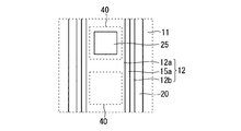
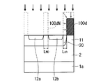
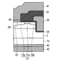
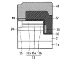
- FIG. 3 is a longitudinal sectional view schematically showing the configuration of the periphery of the semiconductor device (silicon carbide MOSFET) according to the first embodiment, and corresponds to the A1-A2 section shown in FIG. In the figure, the outermost unit cell 10 and the outer end region are shown.
- the MOSFET includes a semiconductor substrate 1a formed of a first conductivity type (n-type) silicon carbide and a first conductivity type drift layer 2 (silicon carbide semiconductor) epitaxially grown on the surface thereof. Layer).
- a drain electrode 43 is formed on the back side of the semiconductor substrate 1a via an ohmic electrode 42 that is in ohmic contact with the semiconductor substrate 1a.
- drift layer 2 a plurality of well regions 20 of the second conductivity type (p-type) are selectively formed in the surface layer portion of the active region 7. A portion 11 adjacent to the well region 20 in the surface layer portion of the drift layer 2 is called a “JFET region”.
- the first conductivity type source region 12 is selectively formed in the surface layer portion of the well region 20.
- a portion between the source region 12 and the JFET region 11 in the well region 20 is a region where a channel is formed when the MOSFET is turned on, and is referred to as a “channel region”.
- each of the source regions 12 includes a source contact region 12a of a first conductivity type, a source extension region 12b, and a source resistance control region 15a.
- the source contact region 12a is connected to the source pad 41 through an ohmic electrode 40 that is in ohmic contact therewith.
- the source resistance control region 15a is formed so as to surround the outside of the source contact region 12a.
- the source extension region 12b is formed so as to surround the outside of the source resistance control region 15a.
- the source extension region 12b is the outermost peripheral portion of the source region 12 and is adjacent to the channel region.
- the source resistance control region 15a is set to have a lower impurity concentration than the source contact region 12a and the source extension region 12b.
- the impurity concentration of the source contact region 12a and the impurity concentration of the source extension region 12b may be approximately the same.
- the source contact region 12a and the source extension region 12b can be formed at the same time, and in this case, both have the same impurity distribution.
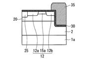
- a well contact region 25 of a second conductivity type connected to the source pad 41 through the ohmic electrode 40 is formed inside the source contact region 12a.
- the well contact region 25 penetrates the source contact region 12 a and reaches the well region 20, and electrically connects the source pad 41 and the well region 20.
- the gate electrode 35 is formed on the drift layer 2 via the gate insulating film 30 and extends across the source extension region 12b, the well region 20 (channel region), and the JFET region 11.
- the source extension region 12 b forms a MOS structure together with the gate insulating film 30 and the gate electrode 35.
- a second conductivity type termination well region 21 is formed in the surface layer portion of the drift layer 2.
- a second conductivity type termination low resistance region 28 connected to the source pad 41 through the ohmic electrode 40 is formed in the surface layer portion of the termination well region 21, a second conductivity type termination low resistance region 28 connected to the source pad 41 through the ohmic electrode 40 is formed. Therefore, the source pad 41 is connected to the source contact region 12 a and is also electrically connected to the well region 20 and the termination well region 21 via the well contact region 25 and the termination low resistance region 28.
- the termination well region 21 and the well region 20 can be formed at the same time. In this case, both have the same impurity distribution.
- a second conductivity type FLR region 50 is formed in the surface layer portion of the drift layer 2 at the outer peripheral portion of the termination well region 21. Furthermore, the first conductivity type field stop region 13 is formed at a position spaced from the terminal well region 21 so as to surround the outside of the FLR region 50.
- a field oxide film 31 is formed in a portion where the gate insulating film 30 is not formed.
- a part of the gate electrode 35 extends to the field oxide film 31, and the gate electrode 35 and the gate wiring 44 are connected at this part.
- the gate electrode 35 is covered with an interlayer insulating film 32, and the source pad 41, the gate wiring 44 and the gate pad 45 are formed thereon. Therefore, in the interlayer insulating film 32, a contact hole (source contact hole) for connecting the source pad 41 to the source contact region 12a, the well contact region 25 and the terminal low resistance region 28, and a gate wiring 44 are connected to the gate electrode 35. A contact hole (gate contact hole) to be formed is formed.
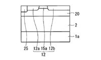
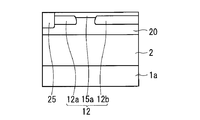
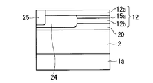
- FIG. 4 is a diagram schematically showing a planar structure of the outermost surface portion of the unit cell 10.
- the source region 12 is composed of three regions: the source contact region 12a, the source extension region 12b, and the source resistance control region 15a therebetween.
- the ohmic electrode 40 for connecting the source pad 41 to the unit cell 10 is formed.
- the ohmic electrode 40 is in contact with only the source contact region 12a among the three regions. Therefore, the source contact region 12 a, the source resistance control region 15 a, and the source extension region 12 b are connected in series between the ohmic electrode 40 and the channel region of the well region 20. Since the source contact region 12a has a high impurity concentration, ohmic contact with a low contact resistance is realized with the ohmic electrode 40.
- the drain current (on-current) flowing from the drain electrode 43 into the drift layer 2 passes through the channel region formed in the surface portion (channel region) of the JFET region 11 and the well region 20. Then, it flows through a path extending from the ohmic electrode 40 to the source electrode 41 through the source extension region 12b, the source resistance control region 15a, and the source contact region 12a.
- the source resistance control region 15a is formed to have a uniform length (current path length) in the direction in which the on-current flows, that is, the direction from the source extension region 12b to the source contact region 12a. .
- the corners of the outer periphery of the source contact region 12a (the inner periphery of the source resistance control region 15a) and the inner periphery of the source extension region 12b (the outer periphery of the source resistance control region 15a) have a round shape.
- the center of the outer peripheral radius of curvature of 12a and the center of the inner peripheral radius of curvature of the source extension region 12b are the same.
- the length of the source resistance control region 15a is made uniform in the unit cell 10, the variation in the source resistance can be suppressed. Accordingly, when an excessive current such as a short-circuit current is instantaneously applied, the current can be prevented from being concentrated on a specific portion, and the reliability of the semiconductor device can be improved. Experimental results showing this effect will be described later.
- the outer peripheral corner portion of the source extension region 12b may be rounded, and the center of curvature radius thereof may be the same as the center of outer periphery curvature radius of the source contact region 12a and the inner periphery curvature radius center of the source extension region 12b.
- the parasitic resistance of the source extension region 12b is made uniform in the unit cell 10.
- the outer peripheral corner portion of the well region 20 is also rounded, and the center of curvature radius thereof is the same as the center of outer peripheral curvature radius of the source contact region 12a and the inner peripheral curvature radius center of the source extension region 12b, thereby uniformizing the channel length. May be.
- the channel resistance is made uniform, variations in device characteristics and current distribution are suppressed, and a more reliable unit cell 10 structure is obtained.
- the unit cell 10 may have any shape, for example, a hexagon, an octagon, or a circle.
- the MOSFET does not have to have a cell structure composed of a plurality of unit cells 10, and may have a comb-like structure as shown in FIG. In general, the comb structure is easy to form, but since the channel width density is lower than that of the cell structure, the on-resistance of the element is relatively high.
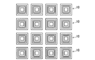
- unit cells 10 are arranged in a matrix as shown in FIG. 6.
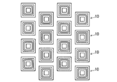
- unit cells 10 are staggered as shown in FIG. You may arrange.
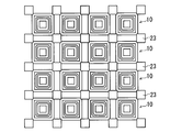
- the second conductivity type well bridge region 23 may be formed so as to bridge the corner portions of the well region 20.
- the well bridge region 23 may be formed in a process different from the well region 20, but if formed at the same time as the ion implantation for forming the well region 20, an increase in the mask pattern forming step and the ion implantation step can be suppressed, and the semiconductor device Manufacturing costs can be reduced.
- FIGS. 9 to 14 are process diagrams for explaining the manufacturing method.
- 9 to 14 correspond to a vertical cross section of the right half of one of the unit cells 10 arranged in the active region 7. That is, FIGS. 9 to 14 do not include the termination region, and show a cross section (cross section along the line B1-B2 in FIG. 1) at an arbitrary position in the region in the active region 7.
- a semiconductor substrate 1a made of silicon carbide of the first conductivity type is prepared.
- other wide band gap semiconductors having a larger band gap than silicon may be used for the semiconductor substrate 1a.
- wide band gap semiconductors include gallium nitride, aluminum nitride, and diamond in addition to silicon carbide.
- the surface orientation of the semiconductor substrate 1a may be arbitrary.
- the surface vertical direction may be inclined by 8 ° or less with respect to the c-axis direction, or may not be inclined.
- the thickness of the semiconductor substrate 1a may be arbitrary and may be, for example, about 350 ⁇ m or about 100 ⁇ m.
- the first conductivity type drift layer 2 is formed on the semiconductor substrate 1a by epitaxial crystal growth.
- the impurity concentration of the first conductivity type of the drift layer 2 is about 1 ⁇ 10 13 cm ⁇ 3 to 1 ⁇ 10 18 cm ⁇ 3 and the thickness is 3 ⁇ m to 200 ⁇ m.
- the impurity concentration distribution of the drift layer 2 is desirably constant in the thickness direction, but may not be constant.
- the impurity concentration may be intentionally increased near the surface, or may be decreased. Good.
- the impurity concentration in the vicinity of the surface of the drift layer 2 is increased, the effect of reducing the resistance of the JFET region 11 to be formed later and the effect of improving the channel mobility can be obtained, and the threshold voltage of the element is set low. be able to.
- the electric field generated in the gate insulating film 30 when a reverse bias is applied to the element is reduced, the reliability of the element is improved, and the threshold voltage of the element can be set high. it can.
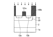
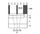
- an implantation mask 100a for example, a resist or a silicon oxide film
- a second conductivity type well region 20 is formed by selective ion implantation using the implantation mask 100a.
- the termination well region 21 is formed in the termination region (not shown).
- the semiconductor substrate 1a is preferably heated at 100 ° C. to 800 ° C., but may not be overheated.
- an impurity (dopant) to be ion-implanted nitrogen or phosphorus is preferable as an n-type impurity, and aluminum or boron is preferable as a p-type impurity.
- the depth of the bottom of the well region 20 needs to be set so as not to exceed the bottom of the drift layer 2 and is, for example, about 0.2 ⁇ m to 2.0 ⁇ m.
- the maximum impurity concentration in the well region 20 exceeds the impurity concentration in the vicinity of the surface of the drift layer 2, and is set within a range of, for example, 1 ⁇ 10 15 cm ⁇ 3 to 1 ⁇ 10 19 cm ⁇ 3 .
- the second conductivity type impurity concentration of the well region 20 is made lower than the first conductivity type impurity concentration of the drift layer 2 in order to increase the conductivity of the channel region. It may be.
- a second conductivity type FLR region 50 is formed in a termination region (not shown).
- the FLR region 50 is also formed by selective ion implantation using a mask (resist or silicon oxide film) processed by photolithography.
- the first conductivity type source contact region 12 a and the first A conductive type source extension region 12b is formed.
- a field stop region 13 of the first conductivity type is formed in the termination region (not shown).
- the depths of the bottoms of the source contact region 12a and the source extension region 12b are set so as not to exceed the bottom of the well region 20. Further, the impurity concentration exceeds the impurity concentration of the well region 20 in each region. For example, the maximum impurity concentration is set to about 1 ⁇ 10 18 cm ⁇ 3 to 1 ⁇ 10 21 cm ⁇ 3 .
- the implantation mask 100bN between the formation region of the source contact region 12a and the formation region of the source extension region 12b defines the length L N0 of the source resistance control region 15a to be formed thereafter.
- L N0 is, for example, 0.1 ⁇ m to 10 ⁇ m, but a range of 0.1 ⁇ m to 1 ⁇ m is effective for suppressing a decrease in channel width density without excessively increasing the cell pitch of the unit cell 10.
- FIG. 15 shows electron micrographs of implantation masks 100b and 100bN used in this step.
- the source contact region 12a and the source extension region 12b are formed between the implantation masks 100b and 100bN.
- FIG. 15 it is observed that the outer peripheral corner portion and the inner peripheral corner portion of the implantation mask 100bN are rounded, and the outer peripheral radius of curvature and the inner peripheral radius of curvature of the implantation mask 100bN are the same. Is done.
- the center of the outer periphery radius of curvature of the source contact region 12a and the center of the inner periphery radius of curvature of the source extension region 12b are the same.
- L N0 can be made uniform in the unit cell 10. In the example shown in FIG. 15, the length of L N0 is 0.7 ⁇ m.
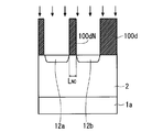
- the MOSFET is miniaturized, the length of the source extension region 12b and source contact regions 12a, and the L N0 is reduced to the extent 1 ⁇ m below the implantation mask implantation mask 100b shown in FIG. 10, the 100bN It may be difficult to process into such a shape. This is because the aspect ratio of the mask pattern is further increased because it is necessary to secure a sufficient mask thickness to ensure the function as an implantation mask.
- the implantation mask 100bN formed on the formation region of the source resistance control region 15a has a high aspect ratio and is difficult to form.
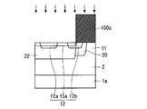
- an implantation mask 101a made of a silicon oxide film, polycrystalline silicon, or the like is formed on the formation region of the source resistance control region 15a using a dedicated fine pattern forming resist or the like. Thereafter, the implantation mask 100b, which may have a relatively low aspect ratio of the mask pattern, may be patterned. If a composite mask composed of the implantation masks 100b and 101a is used, the lengths of the source extension region 12b, the source contact region 12a, and the source resistance control region 15a can be easily reduced.
- first conductivity type source resistance control region 15a is formed using an implantation mask 100c (for example, a resist) processed by photolithography, thereby forming a first conductivity type source resistance control region 15a.
- the impurity concentration of the first conductivity type of the source resistance control region 15a exceeds the second conductivity type impurity concentration of the outermost surface of the well region 20, and is, for example, 1 ⁇ 10 15 cm ⁇ 3 to 1 ⁇ 10 18 cm ⁇ 3 . It is set within the range, more preferably within the range of 1 ⁇ 10 15 cm ⁇ 3 to 1 ⁇ 10 17 cm ⁇ 3 .
- the impurity resistance of the first conductivity type is set lower in the source resistance control region 15a than in the source contact region 12a and the source extension region 12b.
- the impurity concentration of the first conductivity type of the source resistance control region 15a, the source contact region 12a, and the source extension region 12b is made to differ by about 10 to 1000 times.
- the sheet resistance is also different by about 10 to 1000 times.
- the resistance of the source region 12 is intentionally increased by inserting the source resistance control region 15a having a low impurity concentration of the first conductivity type into the source region 12, and in particular, the MOSFET is turned on. More modulation effect is obtained from the resistance level.
- the source contact region 12a and the source extension region 12b reduce the sheet resistance by increasing the impurity concentration of the first conductivity type in order to reduce the parasitic resistance of the MOSFET and further reduce the contact resistance with the ohmic electrode 40. ing.
- the impurity concentration of the first conductivity type in the source resistance control region 15a is 1/10 to 1 of that of the source contact region 12a and the source extension region 12b as described above. / 1000 or so. Further, the thickness of the source resistance control region 15a in the substrate depth direction may be smaller than the thickness of the source contact region 12a and the source extension region 12b in the substrate depth direction.
- the source resistance control region 15a has a sufficiently small impurity concentration and a small thickness with respect to the source contact region 12a and the source extension region 12b. Therefore, even if the source resistance control region 15a is formed to overlap the source contact region 12a and the source extension region 12b as shown in FIG. 12, the impurity concentration of the first conductivity type in the source extension region 12b and the source contact region 12a is increased. Does not have a big impact. Therefore, the source resistance control region 15a is illustrated only between the source extension region 12b and the source contact region 12a in the process diagrams of FIG. 13 and subsequent drawings. However, strictly speaking, the source contact region 12a and the source extension region 12b after the source resistance control region 15a are formed are regions in which the impurity concentration of the first conductivity type is increased in part (overlapping with the source resistance control region 15a). Region).
- the source resistance control region 15a may be formed so as to overlap the entire source contact region 12a and partially overlap the source extension region 12b. In that case, it is possible to reduce the portion that needs to be finely processed in the implantation mask 100c when forming the source resistance control region 15a.
- the source resistance control region 15a may be formed using an implantation mask having an opening only between the source contact region 12a and the source extension region 12b.
- a well contact region 25 having a second conductivity type impurity concentration higher than that of the well region 20 is formed by selective ion implantation. This ion implantation is desirably performed at a substrate temperature of 150 ° C. or higher. By doing so, the well contact region 25 having a low sheet resistance can be formed. The well contact region 25 is formed so that its bottom reaches the well region 20 of the second conductivity type.
- the terminal conductive low-resistance region 28 of the second conductivity type is formed in the well contact region 25 of the termination region (not shown).
- the termination low resistance region 28 can reduce the parasitic resistance of the well contact region 25.
- the termination low resistance region 28 can have a termination region structure with excellent dV / dt resistance.
- the terminal low resistance region 28 may be formed in a process different from the well contact region 25.
- heat treatment for electrically activating impurities implanted into the drift layer 2 is performed.
- This heat treatment is preferably performed in an inert gas atmosphere such as argon or nitrogen or in a vacuum at a temperature of 1500 ° C. to 2200 ° C. for a time of 0.5 to 60 minutes.
- the surface of the drift layer 2 is covered with a film made of carbon, or the surface of the drift layer 2, the back surface of the semiconductor substrate 1, and the end surfaces of the semiconductor substrate 1a and the drift layer 2 are made of carbon. You may go in the state covered with. Thereby, it is possible to prevent the surface of the drift layer 2 from being roughened by etching due to a reaction with residual moisture or residual oxygen in the apparatus during the heat treatment.
- a silicon oxide film (sacrificial oxide film) is formed on the surface of the drift layer 2 by thermal oxidation, and the oxide film is removed by hydrofluoric acid, thereby removing the altered layer on the surface and obtaining a clean surface.
- a silicon oxide film is formed on the drift layer 2 by a CVD (Chemical Vapor Deposition) method or the like, and patterning is performed on the silicon oxide film so as to open the active region 7, thereby providing a region outside the active region 7.
- a field oxide film 31 is formed.
- the thickness of the field oxide film 31 may be 0.5 ⁇ m to 2 ⁇ m.
- a gate insulating film 30 made of a silicon oxide film is formed on the surface of the drift layer 2.
- the method for forming the gate insulating film 30 include a thermal oxidation method and a deposition method. Further, after a silicon oxide film is formed by a thermal oxidation method or a deposition method, a heat treatment in a nitriding oxide gas (NO, N 2 O, etc.) atmosphere or an ammonia atmosphere, or a heat treatment in an inert gas (argon, etc.) atmosphere may be performed. Good.
- polycrystalline silicon or polycrystalline silicon carbide is deposited on the gate insulating film 30 by the CVD method, and patterning is performed by photolithography and etching to form the gate electrode 35. As a result, the structure shown in FIG. 13 is obtained.
- the polycrystalline silicon or polycrystalline silicon carbide used for the gate electrode 35 preferably contains phosphorus, boron, aluminum, or the like and has an n-type or p-type low sheet resistance.
- Phosphorus, boron, or aluminum contained in polycrystalline silicon or polycrystalline silicon carbide may be taken in during the film formation, or may be subjected to activation heat treatment by ion implantation after the film formation.
- the material of the gate electrode 35 may be a metal, an intermetallic compound, or a multilayer film thereof.
- an interlayer insulating film 32 is formed on the drift layer 2 by CVD or the like. Then, a contact hole (source contact hole) for connecting the source pad 41 to the source contact region 12a, the well contact region 25, and the terminal low resistance region 28 is formed in the interlayer insulating film 32 by, for example, dry etching. Further, a contact hole (gate contact hole) for connecting the gate wiring 44 to the gate electrode 35 may be formed at the same time. Thereby, the process steps are simplified and the manufacturing cost can be reduced.
- an ohmic electrode 40 is formed on the surface of the drift layer 2 exposed at the bottom of the source contact hole.
- the ohmic electrode 40 realizes ohmic contact with the source contact region 12a, the well contact region 25, and the terminal low resistance region 28.
- a metal film containing Ni as a main component is formed on the entire surface of the drift layer 2 including the inside of the source contact, and reacted with silicon carbide by heat treatment at 600 to 1100 ° C. to form the ohmic electrode 40.
- a gate contact hole is formed in the previous step, an ohmic electrode made of silicide is also formed at the bottom of the gate contact hole. If the gate contact hole is not formed in the previous step, the gate contact hole to be filled later by the gate wiring 44 is formed by photolithography and etching.
- the entire ohmic electrode 40 may be made of the same intermetallic compound, and the portion connected to the p-type region and the portion connected to the n-type region are made of different intermetallic compounds suitable for each. It may be. It is important for reducing the on-resistance of the MOSFET that the ohmic electrode 40 has a sufficiently low ohmic contact resistance with respect to the source contact region 12a of the first conductivity type. On the other hand, that the ohmic electrode 40 has a sufficiently low ohmic contact resistance with respect to the second conductivity type well contact region 25 is that the well region 20 is fixed to the ground potential or the forward characteristics of the body diode built in the MOSFET. It is preferable from the viewpoint of improvement.
- Both of these can be realized by separately forming a portion connected to the p-type region and a portion connected to the n-type region in the ohmic electrode 40. This can be realized by performing patterning of the metal film for forming the silicide film by using photolithography.
- a silicide film to be the ohmic electrode 42 is formed on the back surface of the semiconductor substrate 1 by the same method.
- the ohmic electrode 42 is in ohmic contact with the semiconductor substrate 1a, and a good connection is realized between the drain electrode 43 to be formed thereafter and the semiconductor substrate 1a.
- a predetermined metal film is formed by sputtering or vapor deposition, and patterned to form a source pad 41, a gate wiring 44, and a gate pad 45 on the interlayer insulating film 32.
- the metal film include Al, Ag, Cu, Ti, Ni, Mo, W, Ta, nitrides thereof, laminated films thereof, alloy films thereof, and the like.
- a drain electrode 43 is formed by forming a metal film such as Ti, Ni, Ag, or Au on the ohmic electrode 42 on the back surface of the semiconductor substrate 1a, thereby completing the MOSFET having the configuration shown in FIG.
- the formed MOSFET may be covered with a protective film such as a silicon nitride film or polyimide.
- This protective film has openings on the gate pad 45 and the source pad 41 so that the gate pad 45 and the source pad 41 can be connected to an external control circuit.
- the semiconductor substrate 1a may be ground from the back surface side to reduce the thickness to about 100 ⁇ m.
- the ground surface is cleaned after thinning, a metal film mainly composed of Ni is formed on the entire back surface, and then a silicide film is formed on the back surface of the semiconductor substrate 1a by a local heating method such as laser annealing.
- the ohmic electrode 42 is formed.
- a drain electrode 43 made of a metal film such as Ti, Ni, Ag, or Au is formed on the ohmic electrode 42.
- the second conductivity type impurity is ion-implanted using the implantation mask 100c at that time.
- the high impurity concentration well region 22 narrower than the well region 20 may be formed.
- FIG. 17 shows the structure of the MOSFET when the high impurity concentration well region 22 is provided.
- the high impurity concentration well region 22 can increase the impurity concentration of the second conductivity type of the well region 20 to reduce the sheet resistance, thereby reducing the switching loss due to the delay of charge transport during the switching operation of the MOSFET. In addition, reliability can be improved.
- the impurity concentration distribution of the second conductivity type in the high impurity concentration well region 22 is desirably low concentration at a shallow position of the drift layer 2 and high concentration at a deep position. By doing so, it is possible to increase the impurity concentration of the second conductivity type in the well region 20 while suppressing the influence on the effective impurity concentration in the source resistance control region 15a where the impurity concentration of the first conductivity type is low.
- the depth of the high impurity concentration well region 22 may be deeper than the well region 20, the same depth, or a shallow depth.
- a MOSFET is shown as an example of a semiconductor device to which the present invention is applied.
- a second conductivity type semiconductor substrate is used instead of the first conductivity type semiconductor substrate 1a.
- the present invention can also be applied to an IGBT using 1b.
- the source region 12 is an “emitter region”
- the well region 20 is a “base region”
- the semiconductor substrate 1 b is a “collector region”.
- the emitter resistance can be increased, so that the emitter region (source region 12), base region (well)
- the current gain in the parasitic transistor composed of the region 20) and the drift layer 2 can be reduced, and as a result, the effect of preventing the latch-up caused by the operation of the IGBT parasitic thyristor can be obtained.
- the effective source resistance can be changed by changing the impurity concentration of the source resistance control region 15a.
- the drain saturation current that affects the magnitude of the short-circuit tolerance is proportional to the square of the gate / source voltage applied to the channel, but in the presence of significant source resistance as in the present invention, the effective gate / The source-to-source voltage is reduced by the product of the source resistance and the drain current. Therefore, if the source resistance is increased, the saturation current is reduced and the short-circuit tolerance can be increased.
- the impurity concentration of the first conductivity type in the source region is substantially uniform in the lateral direction as in the conventional MOSFET, when the source resistance is increased, the contact resistance between the source region and the source pad (ohmic electrode) is increased. As a result, the loss of the device further increases.
- the ohmic electrode 40 connected to the source pad 41 contacts only the low resistance source contact region 12a and does not contact the high resistance source resistance control region 15. Therefore, the contact resistance between the ohmic electrode 40 and the source region 12 is kept low. Therefore, the source resistance can be designed so that the saturation current is reduced while suppressing an excessive increase in the on-resistance.
- the mobility of conduction carriers (electrons or holes) in the source resistance control region 15a is strongly influenced by lattice scattering and becomes lower as the temperature increases. That is, the electrical resistance increases as the temperature increases. Since the source resistance control region 15a has a lower impurity concentration of the first conductivity type than the source contact region 12a and the source extension region 12b, the rate of increase in electrical resistance at a high temperature is higher than those.
- the present inventors have confirmed that when the element is short-circuited, the temperature increases to 1000 K immediately before the breakdown due to the heat generated by the high drain current (Joule heat).
- the resistance of the source resistance control region 15a increases as the temperature increases. Negative feedback functions to reduce the drain current by decreasing the effective gate voltage applied to the channel region. Therefore, the time until the temperature rises to about 1000 K can be extended, and the short circuit resistance can be greatly improved.
- the source extension region 12b has the same impurity concentration distribution of the first conductivity type as the source contact region 12a and has a low sheet resistance.
- the end portion on the source side of the channel region has a gate insulating film 30 and a gate electrode 35 immediately above the end portion, and the end portion is disposed on the inner side of the end portion of the gate electrode 35. The overlap is necessary to reduce the connecting resistance with the channel region.
- implantation and activation annealing of the formation of the source region are performed after the formation of the gate electrode, which is widely applied in the manufacture of semiconductor devices using conventional silicon. Since the self-aligned process to be performed cannot be applied, the source region and the gate electrode are installed with a sufficient margin for misalignment in the photoengraving process at the time of patterning the source region and the gate electrode. Therefore, in the source region, the region overlapping the gate electrode has a low resistance because carriers are accumulated at the MOS interface during the ON operation, but in the region not overlapping with the gate electrode, the sheet resistance itself affects the source resistance. Effect.
- the region length that does not overlap with the gate electrode contributes to the magnitude of the saturation current.
- the source resistance may vary in the unit cell 10 (the path length is shortened when the overlap amount is large, the source resistance is decreased, and the path length is decreased when the overlap amount is small). Becomes longer and the source resistance increases). This causes an unbalance in the unit cell 10 of the saturation current value, which is not preferable.
- the source extension region 12b that overlaps the gate electrode 35 is set to have a low sheet resistance to such an extent that it has little effect on effective gate voltage reduction. Further, the source resistance control region 15 a does not overlap with the gate electrode 35.
- the path length of the source resistance control region 15a that is, the distance between the source contact region 12a and the source extension region 12b is determined by one photolithography process (FIGS. 10 and 15) and does not depend on the alignment accuracy. Therefore, it is possible to prevent the unbalance in the unit cell 10 of the saturation current from occurring.
- the present inventors made a prototype of the semiconductor element according to the present embodiment and conducted an experiment to evaluate its electrical characteristics. The experimental results are shown below.
- FIG. 19 is a graph showing the relationship between the drain current density and the drain voltage of the silicon carbide MOSFET.
- element A is a prototype silicon carbide MOSFET according to the present embodiment
- element B and “element C” are conventional silicon carbide MOSFETs manufactured as comparison targets.
- FIG. 20 shows the channel length, threshold voltage, and on resistance of each of the elements A, B, and C (the on resistance is a value when the drain current density is 100 A / cm 2 ).
- the element A has a source resistance control region 15a, has a channel length of 0.4 ⁇ m, a threshold voltage of 2.5 V, and an on-resistance of 16 m ⁇ cm 2 .
- the element B does not have the source resistance control region 15a, but has a channel length of 0.4 ⁇ m which is the same as the element A. Since the element B has the same channel structure as the element A, the threshold voltage is 2.3 V, which is the same as that of the element A.
- the element C does not have the source resistance control region 15a, but has a longer channel length so that the on-resistance is equal to that of the element A. Specifically, the channel length of the element C is 0.8 ⁇ m, and the on-resistance is 15 m ⁇ cm 2 .
- the element A has a higher on-resistance than the element B by the amount of having the source resistance control region 15a. Further, it can be seen from the experimental results of FIG. 19 that the element A has better drain current saturation characteristics. This is because the saturation characteristic is degraded in the element B due to the short channel effect, whereas in the element A, the effective gate voltage is decreased due to the voltage drop in the source resistance control region 15a, so that the saturation due to the short channel effect occurs. This is considered to be because the deterioration of characteristics is suppressed.
- MOSFETs have the effect of improving MOS channel characteristics (increasing channel mobility) due to heat generation during high bias.
- MOSFETs have the effect of improving MOS channel characteristics (increasing channel mobility) due to heat generation during high bias.
- the drain current at the time of high bias increases due to the effect.
- the effective gate voltage decreases due to the voltage drop in the source resistance control region 15a, and the effect is offset. Since the increase is suppressed, it is considered that a saturation characteristic superior to that of the element C can be obtained.
- the semiconductor element having the source resistance control region 15a has excellent saturation characteristics. This means an improvement in the short-circuit resistance, and one effect of the present invention appears.
- the source region 12 has the source contact region 12a in contact with the ohmic electrode 40 connected to the source pad 41, and the source extension region 12b adjacent to the channel region. Since the source resistance control region 15a between them is connected in series, the saturation current can be controlled by the source resistance corresponding to the sheet resistance of the source resistance control region 15a.
- the source extension region 12b and the source contact region 12a are formed at the same time and the effective impurity concentration distributions of the first conductivity type are the same, it is possible to reduce the manufacturing cost by reducing the number of process steps and to form fine patterning. As a result, it is possible to easily improve manufacturing and to control the length of the source resistance control region 15a sandwiched between the two.
- the impurity concentration distribution of the first conductivity type in the source resistance control region 15a is uniform in the direction from the source extension region 12b to the source contact region 12a, the design value of the source resistance realized in the source resistance control region 15a. This increases the controllability of the product and improves the manufacturing robustness.
- the source resistance control region 15a has a uniform distance in the unit cell 10 in the direction from the source extension region 12b to the source contact region 12a, the current distribution in the unit cell 10 and the heat generation distribution at the time of load short-circuit are uniform. As a result, the reliability with respect to element destruction accompanied by heat generation such as when a load is short-circuited is improved.
- the impurity concentration of the first conductivity type in the source resistance control region 15a is made one digit or less smaller than the first conductivity type impurity concentration of the source extension region 12b or the source contact region 12a (1/10 or less). ) By increasing the sheet resistance of the source resistance control region 15a, a significant source resistance can be given to the on-resistance of the semiconductor device, and the effects of reducing the saturation current and increasing the short-circuit resistance can be achieved.
- the sheet of the source resistance control region 15a Even if the depth of the first conductivity type impurity concentration in the source resistance control region 15a is shallower than the first conductivity type impurity concentration of the source extension region 12b or the source contact region 12a, the sheet of the source resistance control region 15a The resistance is increased, a significant source resistance can be given to the on-resistance of the semiconductor device, and the same effect can be obtained.
- the ion implantation for forming the source contact region 12a and the source extension region 12b and the ion implantation for forming the source resistance control region 15a are performed in separate steps. 2 proposes a technique for performing them in a single ion implantation step.
- FIG. 21 is a diagram for describing the method for manufacturing the silicon carbide MOSFET which is the semiconductor device according to the second embodiment.
- the implantation mask 101a formed on the formation region of the source resistance control region 15a in the process described with reference to FIG. 11 in the first embodiment is thin as shown in FIG. Replace with implantation mask 101b.
- the thickness of the implantation mask 101b is set such that a part of the impurity penetrates during ion implantation of the first conductivity type impurity for forming the source contact region 12a and the source extension region 12b.
- the source resistance control region 15a having a low impurity concentration and a small thickness can be formed by the impurities that have passed through the implantation mask 101b. . That is, the source contact region 12a, the source extension region 12b, and the source resistance control region 15a can be formed simultaneously.
- FIG. 22 is a diagram showing a result of numerical calculation of the impurity concentration distribution of the first conductivity type in the source region 12 formed in the silicon carbide semiconductor by the above method. This numerical calculation is based on the assumption that a silicon oxide film is used as the implantation mask 101b, the thickness thereof is 450 nm, and nitrogen is implanted at 110 keV.
- the regions not covered with the implantation mask 101b include regions corresponding to the source extension region 12b and the source contact region 12a having a depth of about 0.30 ⁇ m and a maximum nitrogen concentration of 1 ⁇ 10 19 cm ⁇ 3 or more. Has been obtained.
- a region corresponding to the source resistance control region 15a having a depth of about 0.05 ⁇ m and a nitrogen concentration of about 1 ⁇ 10 16 to 1 ⁇ 10 18 cm ⁇ 3 is obtained.
- the manufacturing process is simplified.
- a tapered implantation mask 101c having inclined sidewalls may be used instead of the highly rectangular implantation mask 101b shown in FIG. 21, a tapered implantation mask 101c having inclined sidewalls may be used.
- the source resistance control region 15a is formed by impurities that have passed through the inclined surface of the implantation mask 101c. Therefore, the impurity concentration of the formed source resistance control region 15a is not constant in the lateral direction, but has a distribution that continuously decreases toward the center.
- the thickness of the implantation mask 101c and the impurity implantation conditions are set so that the central portion of the formed source resistance control region 15a effectively exhibits the first conductivity type.
- Such an impurity concentration distribution in the source resistance control region 15a is obtained by rotating ion implantation from an oblique direction with respect to the surface of the drift layer 2 using a highly rectangular implantation mask 101b as shown in FIG. It can also be formed by performing.
- the width of the implantation mask 100cN formed on the formation region of the source resistance control region 15a is reduced. May be.
- the width of the implantation mask 101cN is smaller than the sum of the lateral spread of the impurity in the ion implantation for forming the source contact region 12a and the lateral spread of the impurity in the ion implantation for forming the source extension region 12b. It is about 0.2 ⁇ m. If it is difficult to form the implantation mask 100cN having a sufficiently narrow width, the width may be reduced by a process such as trimming after the implantation masks 100c and 100cN having a slightly wider width are formed.
- the source contact region 12a and the source extension region 12b are formed at a deep position in the drift layer 2 due to lateral scattering of the implanted impurities.
- the region 12b comes into contact with the source resistance control region 15a having a low first conductivity type impurity concentration. That is, the source contact region 12a, the source extension region 12b, and the source resistance control region 15a can be formed simultaneously.
- FIG. 25 is a diagram showing a result of numerical calculation of the impurity concentration distribution of the first conductivity type in the source region 12 formed in the silicon carbide semiconductor by the above method. This numerical calculation is based on the assumption that nitrogen is implanted at 110 keV using an implantation mask having a width of 0.2 ⁇ m.
- FIG. 26 shows a nitrogen concentration distribution in the horizontal direction at a depth of 0.19 ⁇ m. The nitrogen concentration in the region corresponding to the source contact region 12a and the source extension region 12b is about 2 ⁇ 10 19 cm ⁇ 3 , whereas the nitrogen concentration in the region corresponding to the source resistance control region 15a is lower than that. The minimum value is about 1 ⁇ 10 17 cm ⁇ 3 .
- the process of individually forming the source resistance control region 15a can be omitted, so that the manufacturing process can be simplified.
- the thermal diffusion coefficient of impurities in silicon carbide is very small compared to the thermal diffusion coefficient of impurities in silicon conventionally used for power devices, and the impurities implanted by thermal diffusion are also affected by high-temperature heat treatment such as activation annealing. Redistribution hardly occurs and the distribution at the time of injection is almost maintained. Therefore, a steep impurity distribution as shown in FIGS. 25 and 26 can be easily obtained as the final shape of the element.
- the implantation mask 100bN is not formed on the formation region of the source resistance control region 15a, but only the implantation mask 100b is formed as shown in FIG.
- the source region 12 is formed by ion implantation of one conductivity type impurity.
- a recess 26 is formed in the upper portion of the formation region of the source resistance control region 15a, and the source region 12 in that portion is thinned. That is, the recess 26 is shallower than the depth of the source region 12, and the first conductivity type region remains at the bottom of the recess 26.
- the portion of the source region 12 thinned by etching (the first conductivity type region at the bottom of the recess 26) has a high resistance and functions as the source resistance control region 15a. Further, the portions of the source region 12 that are not etched on both sides are maintained at a low resistance, and thus function as the source contact region 12a and the source extension region 12b.
- the source region 12 including the source contact region 12a, the source extension region 12b, and the source resistance control region 15a is formed by performing the ion implantation process only once. Further, according to this method, the resistance value of the source resistance control region 15 a can be controlled by the width and depth of the recess 26.
- the well region 20 is formed after the source contact region 12a and the source extension region 12b are formed.
- FIG. 29 and FIG. 30 are diagrams showing the steps of forming the well region 20, the source contact region 12a, and the source extension region 12b in the present embodiment.
- implantation masks 100d and 100dN having openings on the formation region of the source contact region 12a and the formation region of the source extension region 12b are formed, and the first conductivity type impurities are formed.
- the source extension region 12b and the source contact region 12a are formed.
- the width L N0 of the implantation mask 100dN formed on the formation region of the source resistance control region 15a is set to not more than twice the length (channel length) Lch of the channel region of the well region 20 to be formed later.
- the implantation masks 100d and 100dN are trimmed by etching.
- This trimming is performed by oxygen plasma treatment when the implantation mask 100dN is a resist, and when the implantation mask 100dN is a silicon oxide film, dry trimming using CHF3 gas or the like, hydrofluoric acid or buffered fluoride is performed. Performed by wet etching with acid. The etching amount in the trimming is about the length Lch of the channel region of the well region 20 to be formed later.
- Implant mask 100dN is completely removed by trimming because its width L N0 is not more than twice the length Lch of the channel region.
- the well region 20 is formed by ion-implanting impurities of the second conductivity type using the trimmed implantation mask 100d.
- the length Lch of the channel region of the well region 20 is formed in a self-aligned manner so as to be approximately the same as the trimming amount.
- the implantation mask 100dN on the formation region of the source resistance control region 15a is removed, a uniform well region 20 is also formed below the region.
- the MOSFET structure shown in FIG. 14 is obtained by performing the steps after FIG. 12 described in the first embodiment.
- a uniform well region 20 can be formed under the source resistance control region 15a, and a channel region having a uniform length can be formed in a self-aligned manner.
- the value voltage is uniform in the unit cell 10, and a highly reliable semiconductor device can be obtained.
- FIGS. 31 to 39 are process diagrams showing a method of manufacturing a trench type silicon carbide MOSFET which is a semiconductor device according to the present embodiment. These drawings correspond to the vertical cross section of the right half of one of the unit cells 10 arranged in the active region 7. That is, FIGS. 31 to 39 do not include the termination region, and show a cross section at an arbitrary position of the region in the active region 7.
- the drift layer 2 is formed on the semiconductor substrate 1a. Then, ion implantation into the drift layer 2 is performed in the same procedure as described with reference to FIGS. 9 to 12 to form the source region 12 including the source contact region 12a, the source extension region 12b, and the source resistance control region 15a. To do. Further, the well contact region 25 is formed by selective ion implantation.
- the well region 20 and the source extension region 12b may be connected between the adjacent unit cells 10 (that is, the JFET region 11 may not be formed). Further, since the source resistance control region 15a has a sufficiently low impurity concentration relative to the source extension region 12b and hardly affects the impurity concentration of the source extension region 12b, the source resistance control region 15a is also formed by being connected between the unit cells 10. May be. That is, the implantation mask 100a in FIG. 9, the implantation mask 100b on the right side in FIG. 10 (or FIG. 11), and the implantation mask 100c in FIG. 12 may be omitted. In that case, the structure shown in FIG. 31 is obtained.
- the source contact region 12a and the source extension region 12b may be in contact with the surface of the drift layer 2 as shown in FIG. 31, or may be separated from the surface of the drift layer 2 as shown in FIG.
- the source contact region 12a and the source extension region 12b are formed so as to be embedded in the drift layer 2, and the source resistance control region 15a is formed in the upper layer portion (surface portion of the drift layer 2).
- the source contact region 12a and the source extension region 12b are formed in contact with each other.
- a trench 110 as shown in FIG. 33 is formed in a region between the unit cells 10 by selective etching.
- the trench 110 is formed in contact with the well region 20 and the source extension region 12 b and deeper than the bottom of the well region 20.
- the source extension region 12b and the well region 20 are exposed side by side in the vertical direction (the direction perpendicular to the surface of the drift layer 2, that is, the depth direction of the trench 110) on the sidewall of the trench 110.
- the shape of the corner portion of the trench 110 is desirably a taper shape or a round shape in order to reduce electric field concentration during the operation of the MOSFET. Further, it is desirable that the side wall of the trench 110 is nearly perpendicular to the surface of the drift layer 2.
- the field oxide film 31, the gate oxide film 30 and the gate electrode 35 are obtained in the same manner as in the first embodiment. Form.
- the gate insulating film 30 is formed on the surface of the drift layer 2 including the inside of the trench 110.
- the gate electrode 35 is at least partially embedded in the trench 110, and is adjacent to the source extension region 12 b, the well region 20, and the drift layer 2 exposed on the sidewall of the trench 110 via the gate insulating film 30. Arranged. That is, the gate electrode 35 extends across the source extension region 12 b, the well region 20, and the drift layer 2 exposed on the sidewall of the trench 110. In this case, the portion of the well region 20 sandwiched between the drift layer 2 and the source extension region 12b below the well region 20 and adjacent to the trench 110 becomes the channel region of the MOSFET.
- the gate electrode 35 When the gate electrode 35 is patterned, if the lateral end of the gate electrode 35 is positioned outside the trench 110, a part of the gate electrode 35 is embedded in the trench 110 as shown in FIG. On the other hand, as shown in FIG. 35, the gate electrode 35 may be left only in the trench 110 (side wall portion), and the entire gate electrode 35 may be embedded in the trench 110.
- the gate electrode 35, the interlayer insulating film 32, the ohmic electrode 40, and the source pad 41 are formed by the same procedure as in the first embodiment. Thereby, a trench type silicon carbide MOSFET having the structure shown in FIG. 36 is obtained.
- the configuration of the silicon carbide MOSFET is as shown in FIG.
- gate electrode 35 has the shape shown in FIG. 35
- the structure of silicon carbide MOSFET is as shown in FIG.
- the configuration of the silicon carbide MOSFET is as shown in FIG.
- the width of the gate electrode 35 is increased as shown in FIG. 36 and FIG. 37, there is an advantage that the resistance value of the gate electrode 35 can be sufficiently lowered.
- the edge portion of the trench 110 and the MOS structure portion at the bottom of the trench 110 are advantageous. High electric field tends to occur.
- the gate electrode 35 is formed only on the side wall of the trench 110 as shown in FIGS. 38 and 39, the problem of the high electric field can be avoided and the gate electrode 35 can be formed by a self-alignment process. It can also contribute to cost reduction by reducing the number of sheets.
- the gate electrode 35 is formed so as to be adjacent to the source extension region 12b with the gate insulating film 30 interposed therebetween (overlapping in the lateral direction), which is the channel resistance of the MOSFET. It is important from the viewpoint of preventing the increase of
- the present invention can also be applied to trench type MOSFETs.
- the source resistance control region 15a formed in a different process from the source contact region 12a and the source extension region 12b is inserted in series in the path from the channel region of the well region 20 to the ohmic electrode 40 and the source electrode 41. Therefore, the effective source resistance can be changed by changing the impurity concentration of the source resistance control region 15a, and the same effect as in the first embodiment can be obtained.
- the trench MOSFET has a structure without the JFET region 11, the saturation current cannot be controlled by the JFET effect, but by applying the present invention, the saturation current can be controlled by controlling the source resistance.
- the present invention is applied to a trench-type MOSFET.
- the source region 12 is configured so that the source contact region 12a, the source resistance control region 15a, and the source extension region 12b are vertically arranged.
- a stacked structure arranged in a direction (a direction perpendicular to the surface of the drift layer 2, hereinafter also referred to as a “depth direction”).
- FIGS. 40 to 45 are process diagrams showing a method of manufacturing a trench type silicon carbide MOSFET which is a semiconductor device according to the present embodiment. These drawings correspond to the vertical cross section of the right half of one of the unit cells 10 arranged in the active region 7. That is, FIGS. 40 to 45 do not include the termination region, and show a cross section at an arbitrary position of the region in the active region 7.
- the source region 12 has a three-layer structure in which the source contact region 12a, the source resistance control region 15a, and the source extension region 12b are arranged in the depth direction as shown in FIG.
- the three-layer source region 12 can be formed by an epitaxial growth method, an ion implantation method, or a combination of both. For example, when all the source regions 12 are formed by epitaxial growth, first, a first conductivity type semiconductor to be the source extension region 12b is grown on the well region 20, and then the first conductivity to be the source resistance control region 15a. A first type semiconductor is grown, and a first conductivity type semiconductor to be the source contact region 12a is further grown thereon. In these epitaxial growth processes, the formation conditions are appropriately set so that each of the source contact region 12a, the source resistance control region 15a, and the source extension region 12b has a desired impurity concentration and film thickness.
- the source extension region 12b and the source resistance control region 15a may be formed by epitaxial growth, and the source contact region 12a may be formed by ion implantation. That is, a first conductivity type semiconductor to be the source extension region 12b is grown on the well region 20, a first conductivity type semiconductor to be the source resistance control region 15a is grown thereon, and then the source resistance control region is grown.
- the source contact region 12a may be formed by ion-implanting a first conductivity type impurity into the upper layer portion of 15a.
- the well region 20 may be formed by ion-implanting a second conductivity type impurity in the upper layer portion of the drift layer 2 or may be formed by epitaxially growing a second conductivity type semiconductor on the drift layer 2. May be.
- the well contact region 25 is formed by ion implantation after the source region 12 is formed.
- the source resistance control region 15a When the source resistance control region 15a is formed by the epitaxial growth method, it is not affected by the amount of impurities of the second conductivity type in the well region 20, and has a high quality and low doping amount free from defects (implantation defects) caused by ion implantation. A source resistance control region 15a can be formed. For this reason, the source resistance control region 15a has a high temperature dependence of mobility (shows higher resistance at higher temperatures). When the temperature dependency of the mobility of the source resistance control region 15a is large, the effect of depressing the saturation current at the time of heat generation such as when the element is short-circuited increases, and the effect of improving the short-circuit tolerance of the MOSFET is obtained.
- the source region 12 having a three-layer structure is formed by the epitaxial growth method, selective ion implantation of the second conductivity type impurity is additionally performed, and the source resistance control region 15a and the source extension region are formed as shown in FIG.
- An additional injection well region 24 of the second conductivity type overlapping a part of 12b may be formed.
- the width of the source resistance control region 15a and the source extension region 12b is narrowed, and the resistance of the source resistance control region 15a is increased. It is possible to further improve the tolerance.
- the additional implantation well region 24 is formed at a position separated from the trench 110 to be formed later.
- the source region 12 having a three-layer structure may be formed by ion implantation of all the first conductivity type impurities.
- the implantation energy and the dose amount in each ion implantation are appropriately set so that the source contact region 12a, the source resistance control region 15a, and the source extension region 12b have a desired formation depth and impurity concentration, respectively.
- the width of the source resistance control region 15a and the source extension region 12b can be set by using an implantation mask, the width of the source resistance control region 15a is not formed as shown in FIG. 42 without forming the additional implantation well region 24. By narrowing, it is possible to further improve the short-circuit tolerance of the MOSFET.
- FIG. 46 shows the well region 20 and the source when the well region 20, the source contact region 12a, the source extension region 12b, and the source resistance control region 15a of the silicon carbide MOSFET according to the present embodiment are all formed by the ion implantation method.
- 6 is a graph showing a numerical calculation result of an impurity concentration distribution in a region 12;
- the horizontal axis of the graph of FIG. 46 is the depth from the surface of the drift layer 2 along the line G1-G2 of FIG.
- nitrogen (N) is used as the first conductivity type impurity
- aluminum (Al) is used as the second conductivity type impurity.
- the region where the concentration of the first conductivity type impurity (N) is higher than the concentration of the second conductivity type impurity (Al) and the depth from the surface of the drift layer 2 is about 0.35 ⁇ m is the source.
- the region having a depth of about 0 to 0.1 ⁇ m is the source contact region 12a
- the region having a depth of about 0.1 to 0.15 ⁇ m is the source resistance control region 15a
- the depth is 0.15 to 0.35 ⁇ m.
- the region of about the extent is the source extension region 12b.
- a region having a depth of about 0.35 to 1.0 ⁇ m is the well region 20.
- Silicon carbide has a very low thermal diffusion coefficient of impurities, and the distribution at the time of implantation is substantially maintained even after high-temperature heat treatment for activating the impurities. Therefore, even in a completed MOSFET, the impurity distribution as shown in FIG. 46 can be easily obtained. Obtainable.
- the depth is such that the first-conductivity-type impurity concentration is minimized (at a depth of about 0.1 ⁇ m in FIG. 46).
- the second conductivity type impurity may be additionally implanted.
- the trench 110 is formed so as to penetrate the source region 12 and the well region 20 and reach the drift layer 2 below the well region 20. Since the source region 12 has a structure in which the source contact region 12 a, the source resistance control region 15 a, and the source extension region 12 b are stacked in the depth direction, all of them reach the side wall of the trench 110. As in the fourth embodiment, the channel region of the MOSFET is a portion of the well region 20 sandwiched between the drift layer 2 and the source extension region 12b below the well region 20 and adjacent to the trench 110.
- the entire gate electrode 35 is embedded in the trench 110.
- the gate electrode 35 overlaps a part of the source extension region 12b, but does not overlap the source resistance control region 15a (see FIG. 43). That is, the gate electrode 35 extends so as to straddle the source extension region 12 b, the well region 20, and the drift layer 2. Since the gate electrode 35 overlaps the source extension region 12b, an increase in the channel resistance of the MOSFET can be prevented. In addition, since the gate electrode 35 does not overlap the source resistance control region 15a, the effect of the present invention by the source resistance control region 15a can be made independent of the gate bias.
- the interlayer insulating film 32, the ohmic electrode 40, and the source pad 41 are formed by the same procedure as in the first embodiment, whereby a trench type silicon carbide MOSFET having the configuration shown in FIG. 43 is obtained.
- the semiconductor device of the fifth embodiment since the source extension region 12b, the source resistance control region 15a and the source contact region 12a are arranged in the depth direction, the lateral cell pitch of the unit cell 10 can be reduced.
- the on-resistance of the element can be reduced by increasing the channel density.
- the source resistance control region 15a by the epitaxial growth method, it is possible to obtain a region having no implantation defects and having a low impurity concentration and excellent temperature characteristics, and the short-circuit resistance of the device can be further improved.
- the IGBT of the IGBT can be obtained by using the second conductivity type semiconductor substrate 1b (FIG. 18) instead of the first conductivity type semiconductor substrate 1a. It becomes a structure and this invention is applicable also to IGBT.
- the effects obtained from the structure of the semiconductor device described in the first to third embodiments can be obtained in the same manner even if formed by other manufacturing methods as long as the structure is provided. Further, within the scope of the invention, the present invention can be freely combined with each other, or can be appropriately modified or omitted.
Abstract
Description
図1は、実施の形態1に係る半導体装置である炭化珪素MOSFETの上面構成を模式的に示す図である。また図2は、当該半導体装置の半導体層の最表面の構成を示す図である。つまり、当該半導体装置は、図2に示す半導体層の上に、図1に示す各要素が形成されて構成されている。
実施の形態1では、ソースコンタクト領域12a及びソースエクステンション領域12bを形成するためのイオン注入と、ソース抵抗制御領域15aを形成するためのイオン注入とを別の工程で行っていたが、実施の形態2では、それらを1回のイオン注入工程で行う技術を提案する。
実施の形態3においては、ソースコンタクト領域12a及びソースエクステンション領域12bを形成するための注入マスクと、ウェル領域20を形成するための注入マスクとを、1回の写真製版のみを用いて形成する技術を提案する。
実施の形態4では、本発明をトレンチ形のMOSFETに適用する。図31~図39は、本実施の形態に係る半導体装置であるトレンチ形の炭化珪素MOSFETの製造方法を示す工程図である。これらの図は、能動領域7内に複数配設されたユニットセル10のうちの一つの右側半分の縦断面に相当する。つまり、図31~図39は終端領域を含んでおらず、能動領域7内の領域の任意の位置の断面を示している。
実施の形態5では、実施の形態4と同様に、本発明をトレンチ形のMOSFETに適用するが、ソース領域12の構成を、ソースコンタクト領域12a、ソース抵抗制御領域15a、ソースエクステンション領域12bが縦方向(ドリフト層2の表面に対して垂直な方向、以下「深さ方向」ともいう)に並ぶ積層構造とする。
Claims (19)
- 半導体基板(1a)と、
前記半導体基板(1a)上に形成された第1導電型のドリフト層(2)と、
前記ドリフト層(2)の表層部に選択的に形成された第2導電型のウェル領域(20)と、
前記ウェル領域(20)内の表層部に形成された第1導電型のソース領域(12)と、
前記ウェル領域(20)に隣接する前記ドリフト層(2)の部分であるJFET領域(11)と、
前記ソース領域(12)と前記JFET領域(11)とに挟まれた前記ウェル領域(20)の部分であるチャネル領域と、
前記ドリフト層(2)上にゲート絶縁膜(30)を介して配設され、前記ソース領域(12)、前記チャネル領域および前記JFET領域(11)に跨って延在するゲート電極(35)と、
前記ソース領域(12)に接続するソース電極(41)と、
前記半導体基板(1a)の裏面に形成されたドレイン電極(43)とを備え、
前記ソース領域(12)は、
前記ソース電極(41)に接続するソースコンタクト領域(12a)と、
前記チャネル領域に隣接するソースエクステンション領域(12b)と、
前記ソースエクステンション領域(12b)と前記ソースコンタクト領域(12a)との間に配設され、前記ソースエクステンション領域(12b)および前記ソースコンタクト領域(12a)とは第1導電型の不純物濃度が異なるソース抵抗制御領域(15a)とを含み、
前記ソースコンタクト領域(12a)と前記ソースエクステンション領域(12b)は同じ不純物濃度分布を有しており、
前記ゲート電極(35)は、前記ソース領域(12)のうちの前記ソースエクステンション領域(12b)のみにオーバーラップしている
ことを特徴とする半導体装置。 - 半導体基板(1a)と、
前記半導体基板(1a)上に形成された第1導電型のドリフト層(2)と、
前記ドリフト層(2)の表層部に選択的に形成された第2導電型のウェル領域(20)と、
前記ウェル領域(20)を貫通するように形成されたトレンチ(110)と、
前記ウェル領域(20)内の表層部および前記トレンチ(110)の側壁に形成された第1導電型のソース領域(12)と、
前記ソース領域(12)と前記ドリフト層(2)とに挟まれた前記ウェル領域(20)の部分であって、前記トレンチ(110)の側壁の部分であるチャネル領域と、
前記ドリフト層(2)上にゲート絶縁膜(30)を介して配設され、前記ソース領域(12)および前記チャネル領域に跨って延在するゲート電極(35)と、
前記ソース領域(12)に接続するソース電極(41)と、
前記半導体基板(1a)の裏面に形成されたドレイン電極(43)とを備え、
前記ソース領域(12)は、
前記ソース電極(41)に接続するソースコンタクト領域(12a)と、
前記チャネル領域に隣接するソースエクステンション領域(12b)と、
前記ソースエクステンション領域(12b)と前記ソースコンタクト領域(12a)との間に配設され、前記ソースエクステンション領域(12b)および前記ソースコンタクト領域(12a)とは第1導電型の不純物濃度が異なるソース抵抗制御領域(15a)とを含み、
前記ソースコンタクト領域(12a)と前記ソースエクステンション領域(12b)は同じ不純物濃度分布を有しており、
前記ゲート電極(35)は、前記ソース領域(12)のうちの前記ソースエクステンション領域(12b)のみにオーバーラップしている
ことを特徴とする半導体装置。 - 前記ソース抵抗制御領域(15a)において、第1導電型の不純物濃度分布は、前記ソースエクステンション領域(12b)から前記ソースコンタクト領域(12a)へ向けて連続的に変化している
請求項1または請求項2記載の半導体装置。 - 前記ソース抵抗制御領域(15a)の第1導電型の不純物濃度は、前記ソースエクステンション領域(12b)およびソースコンタクト領域(12a)の第1導電型の不純物濃度よりも1桁以上小さい
請求項1または請求項2記載の半導体装置。 - 前記ソース抵抗制御領域(15a)のシート抵抗は、前記ソースエクステンション領域(12b)およびソースコンタクト領域(12a)のシート抵抗よりも高い
請求項1または請求項2記載の半導体装置。 - 前記ソース抵抗制御領域(15a)における前記ソースエクステンション領域(12b)から前記ソースコンタクト領域(12a)へ向かう方向の長さは均一である
請求項1または請求項2記載の半導体装置。 - 前記ソース抵抗制御領域(15a)における前記ソースエクステンション領域(12b)から前記ソースコンタクト領域(12a)までの長さは、前記チャネル領域の長さの2倍以下である
請求項1または請求項2記載の半導体装置。 - 前記ソースエクステンション領域(12b)、前記ソース抵抗制御領域(15a)および前記ソースコンタクト領域(12a)は、前記トレンチ(110)の側壁に存在する
請求項2記載の半導体装置。 - (a)第1導電型の半導体層(2)の表層部に、第2導電型の不純物をイオン注入することによりウェル領域(20)を形成する工程と、
(b)前記ウェル領域(20)内の表層部に第1導電型の不純物をイオン注入することよりソース領域(12)を形成する工程と、
(c)前記ウェル領域(20)に隣接する前記半導体層(2)の部分であるJFET領域(11)、前記ソース領域(12)と前記JFET領域(11)とに挟まれた前記ウェル領域(20)の部分であるチャネル領域および前記ソース領域(12)に跨がるように、前記半導体層(2)上にゲート絶縁膜(30)を介してゲート電極(35)を形成する工程と、
(d)前記ソース領域(12)に接続するソース電極(41)を形成する工程とを備え、
前記工程(b)は、
(b-1)前記ソース電極(41)に接続する前記ソース領域(12)の部分であるソースコンタクト領域(12a)を形成するイオン注入工程と、
(b-2)前記チャネル領域に隣接する前記ソース領域(12)の部分であるソースエクステンション領域(12b)を形成するイオン注入工程と、
(b-3)前記ソースエクステンション領域(12b)と前記ソースコンタクト領域(12a)とに挟まれた前記ソース領域(12)の部分であるソース抵抗制御領域(15a)を形成するイオン注入工程と、を含み、
前記工程(b-1)及び(b-2)は同時に行われる
ことを特徴とする半導体装置の製造方法。 - (a)第1導電型の半導体層(2)の表層部に、第2導電型の不純物をイオン注入することによりウェル領域(20)を形成する工程と、
(b)前記ウェル領域(20)内の表層部に第1導電型の不純物をイオン注入することよりソース領域(12)を形成する工程と、
(c)前記ソース領域(12)および前記ウェル領域(20)を貫通して前記ウェル領域(20)の下の前記半導体層(2)に達するトレンチ(110)を形成する工程と、
(d)前記トレンチ(110)の側壁に露出した、前記ソース領域(12)、前記半導体層(2)、および当該ソース領域(12)と当該半導体層(2)との間の前記ウェル領域(20)の部分であるチャネル領域に跨がるように、前記トレンチ(110)の側壁にゲート絶縁膜(30)を介してゲート電極(35)を形成する工程と、
(e)前記ソース領域(12)に接続するソース電極(41)を形成する工程とを備え、
前記工程(b)は、
(b-1)前記ソース電極(41)に接続する前記ソース領域(12)の部分であるソースコンタクト領域(12a)を形成するイオン注入工程と、
(b-2)前記チャネル領域の上に接する前記ソース領域(12)の部分であるソースエクステンション領域(12b)を形成するイオン注入工程と、
(b-3)前記ソースエクステンション領域(12b)と前記ソースコンタクト領域(12a)とに挟まれた前記ソース領域(12)の部分であるソース抵抗制御領域(15a)を形成するイオン注入工程と、を含み、
前記工程(b-1)及び(b-2)は同時に行われる
ことを特徴とする半導体装置の製造方法。 - 前記工程(b)は、
(b-4)前記ソース抵抗制御領域(15a)の形成領域上に、前記工程(b-2)のイオン注入で不純物の一部が貫通する薄いマスク(101b)を形成する工程を含み、
前記工程(b-1)、(b-2)及び(b-3)は、前記工程(b-4)の後に同時に行われる
請求項9または請求項10記載の半導体装置の製造方法。 - 前記工程(b-4)で形成される前記マスク(101c)はテーパー形状である
請求項11記載の半導体装置の製造方法。 - 前記工程(b)は、
(b-4)前記ソース抵抗制御領域(15a)の形成領域上に、前記(b-1)及び(b-2)のイオン注入における前記半導体層(2)内での不純物の横方向の広がりの和よりも狭いマスク(100cN)を形成する工程を含み、
前記工程(b-3)は、前記マスク(100cN)を挟んで前記工程(b-1)及び(b-2)のイオン注入を行うことにより実施される
請求項9または請求項10記載の半導体装置の製造方法。 - 前記工程(b)は、
(b-4)前記ソースエクステンション領域(12b)および前記ソースコンタクト領域(12a)の形成領域が開口され、前記ソース抵抗制御領域(15a)の形成領域を覆う第1のマスク(100d,100dN)を形成する工程を含み、
前記工程(b-1)及び(b-2)のイオン注入は前記第1のマスク(100d,100dN)を用いて行われ、
前記工程(a)は、
(a-1)前記第1のマスク(100d,100dN)の側面を後退させることにより第2のマスク(100d)を形成する工程と、
(a-2)前記第2のマスク(100d)を用いたイオン注入により前記ウェル領域(20)を形成する工程とを含み、
前記工程(a-1)において、前記第1のマスク(100d,100dN)における前記ソース抵抗制御領域(15a)の形成領域を覆う部分(100dN)は除去される
請求項9または請求項10記載の半導体装置の製造方法。 - (a)第1導電型の半導体層(2)の表層部に、第2導電型のウェル領域(20)を形成する工程と、
(b)前記ウェル領域(20)内の表層部に、第1導電型のソース領域(12)を形成する工程と、
(c)前記ソース領域(12)および前記ウェル領域(20)を貫通して前記ウェル領域(20)の下の前記半導体層(2)に達するトレンチ(110)を形成する工程と、
(d)前記トレンチ(110)の側壁に露出した、前記ソース領域(12)、前記半導体層(2)、および当該ソース領域(12)と当該半導体層(2)との間の前記ウェル領域(20)の部分であるチャネル領域に跨がるように、前記トレンチ(110)の側壁にゲート絶縁膜(30)を介してゲート電極(35)を形成する工程と、
(e)前記ソース領域(12)に接続するソース電極(41)を形成する工程とを備え、
前記工程(b)は、
(b-1)前記チャネル領域の上に接する前記ソース領域(12)の部分であるソースエクステンション領域(12b)を形成する工程と、
(b-2)前記ソースエクステンション領域(12b)の上に接し、前記ソースエクステンション領域(12b)とは第1導電型の不純物濃度が異なるソース抵抗制御領域(15a)を形成する工程と、
(b-3)前記ソース抵抗制御領域(15a)の上に接し、前記ソース抵抗制御領域(15a)とは第1導電型の不純物濃度が異なり、前記ソース電極(41)に接続する前記ソース領域(12)の部分であるソースコンタクト領域(12a)を形成する工程と、を含む
ことを特徴とする半導体装置の製造方法。 - 前記工程(b-1)、(b-2)および(b-3)は、第1導電型の半導体をエピタキシャル成長させることにより行われる
請求項15記載の半導体装置の製造方法。 - 前記工程(b-1)および(b-2)は、第1導電型の半導体をエピタキシャル成長させることにより行われ、
前記工程(b-3)は、前記工程(b-2)で形成された前記ソース抵抗制御領域(15a)の上層部に、第1導電型の不純物をイオン注入することにより行われる
請求項15記載の半導体装置の製造方法。 - 前記工程(b-1)、(b-2)および(b-3)は、前記工程(a)で形成された前記ウェル領域(20)の上層部に、第1導電型の不純物をイオン注入することにより行われる
請求項15記載の半導体装置の製造方法。 - 前記工程(a)は、第2導電型の半導体をエピタキシャル成長させることにより行われる
請求項15から請求項18のいずれか一項記載の半導体装置の製造方法。
Priority Applications (4)
| Application Number | Priority Date | Filing Date | Title |
|---|---|---|---|
| DE112013002518.3T DE112013002518B4 (de) | 2012-05-15 | 2013-03-12 | Halbleiterbauteil und Verfahren zu dessen Herstellung |
| US14/400,025 US9525057B2 (en) | 2012-05-15 | 2013-03-12 | Semiconductor device |
| CN201380025183.6A CN104285301B (zh) | 2012-05-15 | 2013-03-12 | 半导体装置及其制造方法 |
| JP2014515523A JP6144674B2 (ja) | 2012-05-15 | 2013-03-12 | 半導体装置及びその製造方法 |
Applications Claiming Priority (4)
| Application Number | Priority Date | Filing Date | Title |
|---|---|---|---|
| JP2012111266 | 2012-05-15 | ||
| JP2012-111266 | 2012-05-15 | ||
| JP2012-243304 | 2012-11-05 | ||
| JP2012243304 | 2012-11-05 |
Publications (1)
| Publication Number | Publication Date |
|---|---|
| WO2013172079A1 true WO2013172079A1 (ja) | 2013-11-21 |
Family
ID=49583501
Family Applications (1)
| Application Number | Title | Priority Date | Filing Date |
|---|---|---|---|
| PCT/JP2013/056785 WO2013172079A1 (ja) | 2012-05-15 | 2013-03-12 | 半導体装置及びその製造方法 |
Country Status (5)
| Country | Link |
|---|---|
| US (1) | US9525057B2 (ja) |
| JP (1) | JP6144674B2 (ja) |
| CN (1) | CN104285301B (ja) |
| DE (1) | DE112013002518B4 (ja) |
| WO (1) | WO2013172079A1 (ja) |
Cited By (14)
| Publication number | Priority date | Publication date | Assignee | Title |
|---|---|---|---|---|
| CN104157682A (zh) * | 2014-08-25 | 2014-11-19 | 株洲南车时代电气股份有限公司 | 功率半导体芯片的正面结构及其制备方法 |
| JP2015095578A (ja) * | 2013-11-13 | 2015-05-18 | 三菱電機株式会社 | 半導体装置及びその製造方法 |
| JP2015228496A (ja) * | 2014-05-08 | 2015-12-17 | 三菱電機株式会社 | 半導体装置 |
| CN105304702A (zh) * | 2014-07-24 | 2016-02-03 | 住友电气工业株式会社 | 碳化硅半导体器件 |
| CN105304713A (zh) * | 2014-07-24 | 2016-02-03 | 住友电气工业株式会社 | 碳化硅半导体器件 |
| CN107078160A (zh) * | 2014-10-20 | 2017-08-18 | 三菱电机株式会社 | 半导体装置 |
| JP2019046996A (ja) * | 2017-09-04 | 2019-03-22 | 三菱電機株式会社 | 半導体装置、電力変換装置および半導体装置の製造方法 |
| JP2019125724A (ja) * | 2018-01-17 | 2019-07-25 | 富士電機株式会社 | 半導体装置 |
| JP2019216224A (ja) * | 2018-06-14 | 2019-12-19 | 富士電機株式会社 | 半導体装置 |
| JPWO2019123601A1 (ja) * | 2017-12-21 | 2020-07-09 | 三菱電機株式会社 | 半導体装置 |
| WO2020175157A1 (ja) * | 2019-02-27 | 2020-09-03 | 株式会社デンソー | 炭化珪素半導体装置およびその製造方法 |
| JP2020141130A (ja) * | 2019-02-27 | 2020-09-03 | 株式会社デンソー | 炭化珪素半導体装置およびその製造方法 |
| JP2021034624A (ja) * | 2019-08-27 | 2021-03-01 | 株式会社デンソー | トレンチゲート型のスイッチング素子の製造方法 |
| CN114068696A (zh) * | 2020-08-05 | 2022-02-18 | 英飞凌科技股份有限公司 | 包括多个沟槽的半导体装置 |
Families Citing this family (16)
| Publication number | Priority date | Publication date | Assignee | Title |
|---|---|---|---|---|
| JP6183200B2 (ja) * | 2013-12-16 | 2017-08-23 | 住友電気工業株式会社 | 炭化珪素半導体装置およびその製造方法 |
| JP6275282B2 (ja) * | 2015-01-13 | 2018-02-07 | 三菱電機株式会社 | 半導体装置、その製造方法および半導体モジュール |
| DE102015107489B4 (de) * | 2015-05-12 | 2020-07-02 | Infineon Technologies Ag | Verfahren zur Reduzierung des Schichtwiderstands in einer elektronischen Vorrichtung |
| DE102015118616B3 (de) * | 2015-10-30 | 2017-04-13 | Infineon Technologies Austria Ag | Latchup-fester Transistor |
| DE112016006380B4 (de) | 2016-02-09 | 2023-03-09 | Mitsubishi Electric Corporation | Halbleiterbauelement |
| US9899512B2 (en) * | 2016-02-24 | 2018-02-20 | General Electric Company | Silicon carbide device and method of making thereof |
| CN107768250B (zh) * | 2016-08-16 | 2020-10-23 | 比亚迪股份有限公司 | 制备功率半导体器件的方法和功率半导体器件 |
| KR20180129457A (ko) * | 2017-05-26 | 2018-12-05 | 에스케이하이닉스 주식회사 | 반도체 장치 및 그 제조 방법 |
| US10601413B2 (en) * | 2017-09-08 | 2020-03-24 | Cree, Inc. | Power switching devices with DV/DT capability and methods of making such devices |
| US10600897B2 (en) * | 2017-11-08 | 2020-03-24 | Fuji Electric Co., Ltd. | Semiconductor device |
| CN111727506B (zh) * | 2018-02-13 | 2023-05-16 | 新电元工业株式会社 | 半导体装置以及半导体装置的制造方法 |
| US10504995B1 (en) * | 2018-08-09 | 2019-12-10 | Semiconductor Components Industries, Llc | Short-circuit performance for silicon carbide semiconductor device |
| DE102020202053A1 (de) * | 2020-02-19 | 2021-08-19 | Robert Bosch Gesellschaft mit beschränkter Haftung | Mosfet mit sättigungskontakt und verfahren zum bilden eines mosfet mit sättigungskontakt |
| WO2024067997A1 (en) | 2022-09-30 | 2024-04-04 | Hitachi Energy Ltd | Semiconductor device and manufacturing method |
| WO2024067998A1 (en) | 2022-09-30 | 2024-04-04 | Hitachi Energy Ltd | Semiconductor device and manufacturing method |
| CN116013905B (zh) * | 2023-03-27 | 2023-06-23 | 通威微电子有限公司 | 一种半导体器件及其制作方法 |
Citations (4)
| Publication number | Priority date | Publication date | Assignee | Title |
|---|---|---|---|---|
| JPH11312807A (ja) * | 1998-02-27 | 1999-11-09 | Toyota Central Res & Dev Lab Inc | 半導体装置 |
| JP2006120894A (ja) * | 2004-10-22 | 2006-05-11 | Toshiba Corp | 半導体装置 |
| JP2006173584A (ja) * | 2004-11-16 | 2006-06-29 | Toshiba Corp | 半導体装置 |
| JP2009231545A (ja) * | 2008-03-24 | 2009-10-08 | Fuji Electric Device Technology Co Ltd | 炭化珪素mos型半導体装置 |
Family Cites Families (26)
| Publication number | Priority date | Publication date | Assignee | Title |
|---|---|---|---|---|
| JPS62266871A (ja) | 1986-05-15 | 1987-11-19 | Fuji Electric Co Ltd | たて形mosfet |
| US5438220A (en) * | 1987-02-26 | 1995-08-01 | Kabushiki Kaisha Toshiba | High breakdown voltage semiconductor device |
| JP2536302B2 (ja) | 1990-04-30 | 1996-09-18 | 日本電装株式会社 | 絶縁ゲ―ト型バイポ―ラトランジスタ |
| JPH04196174A (ja) | 1990-11-26 | 1992-07-15 | Fuji Electric Co Ltd | 絶縁ゲートバイポーラトランジスタ |
| US6573534B1 (en) * | 1995-09-06 | 2003-06-03 | Denso Corporation | Silicon carbide semiconductor device |
| JPH09283755A (ja) * | 1996-04-18 | 1997-10-31 | Hitachi Ltd | 半導体装置 |
| CN1139134C (zh) * | 1998-01-22 | 2004-02-18 | 三菱电机株式会社 | 绝缘栅型双极型半导体装置 |
| US6528850B1 (en) * | 2000-05-03 | 2003-03-04 | Linear Technology Corporation | High voltage MOS transistor with up-retro well |
| JP4776755B2 (ja) | 2000-06-08 | 2011-09-21 | ルネサスエレクトロニクス株式会社 | 半導体装置およびその製造方法 |
| JP2003332577A (ja) * | 2002-05-16 | 2003-11-21 | Toyota Industries Corp | 半導体装置及びその製造方法 |
| US6940110B2 (en) * | 2002-11-29 | 2005-09-06 | Matsushita Electric Industrial Co., Ltd. | SiC-MISFET and method for fabricating the same |
| ATE514190T1 (de) * | 2003-03-19 | 2011-07-15 | Infineon Technologies Ag | Halbleiteraufbau mit hoch dotiertem kanalleitungsgebiet und verfahren zur herstellung eines halbleiteraufbaus |
| US7569900B2 (en) * | 2004-11-16 | 2009-08-04 | Kabushiki Kaisha Toshiba | Silicon carbide high breakdown voltage semiconductor device |
| JP2006339444A (ja) | 2005-06-02 | 2006-12-14 | Fujitsu Ltd | 半導体装置及びその半導体装置の製造方法 |
| JP2007013058A (ja) * | 2005-07-04 | 2007-01-18 | Toshiba Corp | 半導体装置 |
| US20070034941A1 (en) * | 2005-08-15 | 2007-02-15 | International Rectifier Corp. | Deep N diffusion for trench IGBT |
| JP2007335463A (ja) | 2006-06-12 | 2007-12-27 | Renesas Technology Corp | 静電気放電保護素子および半導体装置 |
| US7776700B2 (en) * | 2007-01-04 | 2010-08-17 | Freescale Semiconductor, Inc. | LDMOS device and method |
| JP4367508B2 (ja) * | 2007-03-13 | 2009-11-18 | 株式会社デンソー | 炭化珪素半導体装置およびその製造方法 |
| US7795691B2 (en) * | 2008-01-25 | 2010-09-14 | Cree, Inc. | Semiconductor transistor with P type re-grown channel layer |
| JP4844621B2 (ja) * | 2008-12-04 | 2011-12-28 | ソニー株式会社 | トランジスタ型保護素子および半導体集積回路 |
| US8723259B2 (en) * | 2009-02-24 | 2014-05-13 | Mitsubishi Electric Corporation | Silicon carbide semiconductor device |
| CN102334190B (zh) * | 2009-04-30 | 2014-05-14 | 三菱电机株式会社 | 半导体装置及其制造方法 |
| JP2012004185A (ja) * | 2010-06-14 | 2012-01-05 | Denso Corp | 炭化珪素半導体装置の製造方法 |
| JP5736683B2 (ja) * | 2010-07-30 | 2015-06-17 | 三菱電機株式会社 | 電力用半導体素子 |
| JP5708550B2 (ja) * | 2012-04-03 | 2015-04-30 | 株式会社デンソー | 炭化珪素半導体装置およびその製造方法 |
-
2013
- 2013-03-12 US US14/400,025 patent/US9525057B2/en active Active
- 2013-03-12 WO PCT/JP2013/056785 patent/WO2013172079A1/ja active Application Filing
- 2013-03-12 CN CN201380025183.6A patent/CN104285301B/zh active Active
- 2013-03-12 DE DE112013002518.3T patent/DE112013002518B4/de active Active
- 2013-03-12 JP JP2014515523A patent/JP6144674B2/ja active Active
Patent Citations (4)
| Publication number | Priority date | Publication date | Assignee | Title |
|---|---|---|---|---|
| JPH11312807A (ja) * | 1998-02-27 | 1999-11-09 | Toyota Central Res & Dev Lab Inc | 半導体装置 |
| JP2006120894A (ja) * | 2004-10-22 | 2006-05-11 | Toshiba Corp | 半導体装置 |
| JP2006173584A (ja) * | 2004-11-16 | 2006-06-29 | Toshiba Corp | 半導体装置 |
| JP2009231545A (ja) * | 2008-03-24 | 2009-10-08 | Fuji Electric Device Technology Co Ltd | 炭化珪素mos型半導体装置 |
Cited By (24)
| Publication number | Priority date | Publication date | Assignee | Title |
|---|---|---|---|---|
| JP2015095578A (ja) * | 2013-11-13 | 2015-05-18 | 三菱電機株式会社 | 半導体装置及びその製造方法 |
| JP2015228496A (ja) * | 2014-05-08 | 2015-12-17 | 三菱電機株式会社 | 半導体装置 |
| JP2016029707A (ja) * | 2014-07-24 | 2016-03-03 | 住友電気工業株式会社 | 炭化珪素半導体装置 |
| CN105304702A (zh) * | 2014-07-24 | 2016-02-03 | 住友电气工业株式会社 | 碳化硅半导体器件 |
| CN105304713A (zh) * | 2014-07-24 | 2016-02-03 | 住友电气工业株式会社 | 碳化硅半导体器件 |
| JP2016029706A (ja) * | 2014-07-24 | 2016-03-03 | 住友電気工業株式会社 | 炭化珪素半導体装置 |
| CN105304702B (zh) * | 2014-07-24 | 2019-04-23 | 住友电气工业株式会社 | 碳化硅半导体器件 |
| CN105304713B (zh) * | 2014-07-24 | 2019-07-19 | 住友电气工业株式会社 | 碳化硅半导体器件 |
| CN104157682A (zh) * | 2014-08-25 | 2014-11-19 | 株洲南车时代电气股份有限公司 | 功率半导体芯片的正面结构及其制备方法 |
| CN107078160A (zh) * | 2014-10-20 | 2017-08-18 | 三菱电机株式会社 | 半导体装置 |
| JP2019046996A (ja) * | 2017-09-04 | 2019-03-22 | 三菱電機株式会社 | 半導体装置、電力変換装置および半導体装置の製造方法 |
| JPWO2019123601A1 (ja) * | 2017-12-21 | 2020-07-09 | 三菱電機株式会社 | 半導体装置 |
| JP7056163B2 (ja) | 2018-01-17 | 2022-04-19 | 富士電機株式会社 | 半導体装置 |
| JP2019125724A (ja) * | 2018-01-17 | 2019-07-25 | 富士電機株式会社 | 半導体装置 |
| JP2019216224A (ja) * | 2018-06-14 | 2019-12-19 | 富士電機株式会社 | 半導体装置 |
| JP7176239B2 (ja) | 2018-06-14 | 2022-11-22 | 富士電機株式会社 | 半導体装置 |
| JP2020141130A (ja) * | 2019-02-27 | 2020-09-03 | 株式会社デンソー | 炭化珪素半導体装置およびその製造方法 |
| CN113498544A (zh) * | 2019-02-27 | 2021-10-12 | 株式会社电装 | 碳化硅半导体装置及其制造方法 |
| WO2020175157A1 (ja) * | 2019-02-27 | 2020-09-03 | 株式会社デンソー | 炭化珪素半導体装置およびその製造方法 |
| JP7140148B2 (ja) | 2019-02-27 | 2022-09-21 | 株式会社デンソー | 炭化珪素半導体装置およびその製造方法 |
| CN113498544B (zh) * | 2019-02-27 | 2023-10-27 | 株式会社电装 | 碳化硅半导体装置及其制造方法 |
| JP2021034624A (ja) * | 2019-08-27 | 2021-03-01 | 株式会社デンソー | トレンチゲート型のスイッチング素子の製造方法 |
| JP7259642B2 (ja) | 2019-08-27 | 2023-04-18 | 株式会社デンソー | トレンチゲート型のスイッチング素子の製造方法 |
| CN114068696A (zh) * | 2020-08-05 | 2022-02-18 | 英飞凌科技股份有限公司 | 包括多个沟槽的半导体装置 |
Also Published As
| Publication number | Publication date |
|---|---|
| US9525057B2 (en) | 2016-12-20 |
| DE112013002518T5 (de) | 2015-04-02 |
| JPWO2013172079A1 (ja) | 2016-01-12 |
| DE112013002518B4 (de) | 2018-01-11 |
| CN104285301B (zh) | 2017-03-08 |
| US20150108564A1 (en) | 2015-04-23 |
| JP6144674B2 (ja) | 2017-06-07 |
| CN104285301A (zh) | 2015-01-14 |
Similar Documents
| Publication | Publication Date | Title |
|---|---|---|
| JP6144674B2 (ja) | 半導体装置及びその製造方法 | |
| US9825126B2 (en) | Semiconductor device | |
| JP6072432B2 (ja) | 半導体装置及びその製造方法 | |
| JP6282088B2 (ja) | 半導体装置及びその製造方法 | |
| JP6049784B2 (ja) | 炭化珪素半導体装置およびその製造方法 | |
| US8658503B2 (en) | Semiconductor device and method of fabricating the same | |
| JP5606529B2 (ja) | 電力用半導体装置 | |
| JP5102411B2 (ja) | 半導体装置およびその製造方法 | |
| US20060267022A1 (en) | Field-effect transistor and thyristor | |
| WO2017169777A1 (ja) | 電力変換器 | |
| WO2017047286A1 (ja) | 半導体装置 | |
| US11489047B2 (en) | Semiconductor device and method of manufacturing the same | |
| JP7399222B2 (ja) | 半導体装置 | |
| JP6869376B2 (ja) | 半導体装置 | |
| JP5751763B2 (ja) | 半導体装置 | |
| US20200161445A1 (en) | Semiconductor device and method of manufacturing the same | |
| JP5907097B2 (ja) | 半導体装置 | |
| JP6289600B2 (ja) | 半導体装置 | |
| JP2015057851A (ja) | 半導体装置 |
Legal Events
| Date | Code | Title | Description |
|---|---|---|---|
| 121 | Ep: the epo has been informed by wipo that ep was designated in this application |
Ref document number: 13790585 Country of ref document: EP Kind code of ref document: A1 |
|
| ENP | Entry into the national phase |
Ref document number: 2014515523 Country of ref document: JP Kind code of ref document: A |
|
| WWE | Wipo information: entry into national phase |
Ref document number: 14400025 Country of ref document: US |
|
| WWE | Wipo information: entry into national phase |
Ref document number: 1120130025183 Country of ref document: DE Ref document number: 112013002518 Country of ref document: DE |
|
| 122 | Ep: pct application non-entry in european phase |
Ref document number: 13790585 Country of ref document: EP Kind code of ref document: A1 |