WO2010082389A1 - 半導体装置およびその製造方法 - Google Patents
半導体装置およびその製造方法 Download PDFInfo
- Publication number
- WO2010082389A1 WO2010082389A1 PCT/JP2009/068275 JP2009068275W WO2010082389A1 WO 2010082389 A1 WO2010082389 A1 WO 2010082389A1 JP 2009068275 W JP2009068275 W JP 2009068275W WO 2010082389 A1 WO2010082389 A1 WO 2010082389A1
- Authority
- WO
- WIPO (PCT)
- Prior art keywords
- insulating film
- gate electrode
- semiconductor device
- region
- forming
- Prior art date
- Legal status (The legal status is an assumption and is not a legal conclusion. Google has not performed a legal analysis and makes no representation as to the accuracy of the status listed.)
- Ceased
Links
Images














Classifications
-
- H—ELECTRICITY
- H10—SEMICONDUCTOR DEVICES; ELECTRIC SOLID-STATE DEVICES NOT OTHERWISE PROVIDED FOR
- H10D—INORGANIC ELECTRIC SEMICONDUCTOR DEVICES
- H10D30/00—Field-effect transistors [FET]
- H10D30/60—Insulated-gate field-effect transistors [IGFET]
- H10D30/69—IGFETs having charge trapping gate insulators, e.g. MNOS transistors
-
- H—ELECTRICITY
- H10—SEMICONDUCTOR DEVICES; ELECTRIC SOLID-STATE DEVICES NOT OTHERWISE PROVIDED FOR
- H10B—ELECTRONIC MEMORY DEVICES
- H10B43/00—EEPROM devices comprising charge-trapping gate insulators
- H10B43/10—EEPROM devices comprising charge-trapping gate insulators characterised by the top-view layout
-
- H—ELECTRICITY
- H10—SEMICONDUCTOR DEVICES; ELECTRIC SOLID-STATE DEVICES NOT OTHERWISE PROVIDED FOR
- H10B—ELECTRONIC MEMORY DEVICES
- H10B43/00—EEPROM devices comprising charge-trapping gate insulators
- H10B43/30—EEPROM devices comprising charge-trapping gate insulators characterised by the memory core region
-
- H—ELECTRICITY
- H10—SEMICONDUCTOR DEVICES; ELECTRIC SOLID-STATE DEVICES NOT OTHERWISE PROVIDED FOR
- H10B—ELECTRONIC MEMORY DEVICES
- H10B43/00—EEPROM devices comprising charge-trapping gate insulators
- H10B43/40—EEPROM devices comprising charge-trapping gate insulators characterised by the peripheral circuit region
-
- H—ELECTRICITY
- H10—SEMICONDUCTOR DEVICES; ELECTRIC SOLID-STATE DEVICES NOT OTHERWISE PROVIDED FOR
- H10B—ELECTRONIC MEMORY DEVICES
- H10B43/00—EEPROM devices comprising charge-trapping gate insulators
- H10B43/50—EEPROM devices comprising charge-trapping gate insulators characterised by the boundary region between the core and peripheral circuit regions
-
- H—ELECTRICITY
- H10—SEMICONDUCTOR DEVICES; ELECTRIC SOLID-STATE DEVICES NOT OTHERWISE PROVIDED FOR
- H10D—INORGANIC ELECTRIC SEMICONDUCTOR DEVICES
- H10D30/00—Field-effect transistors [FET]
- H10D30/01—Manufacture or treatment
- H10D30/021—Manufacture or treatment of FETs having insulated gates [IGFET]
- H10D30/0413—Manufacture or treatment of FETs having insulated gates [IGFET] of FETs having charge-trapping gate insulators, e.g. MNOS transistors
-
- H—ELECTRICITY
- H10—SEMICONDUCTOR DEVICES; ELECTRIC SOLID-STATE DEVICES NOT OTHERWISE PROVIDED FOR
- H10D—INORGANIC ELECTRIC SEMICONDUCTOR DEVICES
- H10D30/00—Field-effect transistors [FET]
- H10D30/60—Insulated-gate field-effect transistors [IGFET]
- H10D30/611—Insulated-gate field-effect transistors [IGFET] having multiple independently-addressable gate electrodes influencing the same channel
-
- H—ELECTRICITY
- H10—SEMICONDUCTOR DEVICES; ELECTRIC SOLID-STATE DEVICES NOT OTHERWISE PROVIDED FOR
- H10D—INORGANIC ELECTRIC SEMICONDUCTOR DEVICES
- H10D30/00—Field-effect transistors [FET]
- H10D30/60—Insulated-gate field-effect transistors [IGFET]
- H10D30/68—Floating-gate IGFETs
- H10D30/6891—Floating-gate IGFETs characterised by the shapes, relative sizes or dispositions of the floating gate electrode
-
- H—ELECTRICITY
- H10—SEMICONDUCTOR DEVICES; ELECTRIC SOLID-STATE DEVICES NOT OTHERWISE PROVIDED FOR
- H10D—INORGANIC ELECTRIC SEMICONDUCTOR DEVICES
- H10D30/00—Field-effect transistors [FET]
- H10D30/60—Insulated-gate field-effect transistors [IGFET]
- H10D30/69—IGFETs having charge trapping gate insulators, e.g. MNOS transistors
- H10D30/694—IGFETs having charge trapping gate insulators, e.g. MNOS transistors characterised by the shapes, relative sizes or dispositions of the gate electrodes
-
- H—ELECTRICITY
- H10—SEMICONDUCTOR DEVICES; ELECTRIC SOLID-STATE DEVICES NOT OTHERWISE PROVIDED FOR
- H10D—INORGANIC ELECTRIC SEMICONDUCTOR DEVICES
- H10D30/00—Field-effect transistors [FET]
- H10D30/60—Insulated-gate field-effect transistors [IGFET]
- H10D30/69—IGFETs having charge trapping gate insulators, e.g. MNOS transistors
- H10D30/694—IGFETs having charge trapping gate insulators, e.g. MNOS transistors characterised by the shapes, relative sizes or dispositions of the gate electrodes
- H10D30/696—IGFETs having charge trapping gate insulators, e.g. MNOS transistors characterised by the shapes, relative sizes or dispositions of the gate electrodes having at least one additional gate, e.g. program gate, erase gate or select gate
-
- H—ELECTRICITY
- H10—SEMICONDUCTOR DEVICES; ELECTRIC SOLID-STATE DEVICES NOT OTHERWISE PROVIDED FOR
- H10D—INORGANIC ELECTRIC SEMICONDUCTOR DEVICES
- H10D62/00—Semiconductor bodies, or regions thereof, of devices having potential barriers
- H10D62/10—Shapes, relative sizes or dispositions of the regions of the semiconductor bodies; Shapes of the semiconductor bodies
- H10D62/113—Isolations within a component, i.e. internal isolations
- H10D62/115—Dielectric isolations, e.g. air gaps
- H10D62/116—Dielectric isolations, e.g. air gaps adjoining the input or output regions of field-effect devices, e.g. adjoining source or drain regions
-
- H—ELECTRICITY
- H10—SEMICONDUCTOR DEVICES; ELECTRIC SOLID-STATE DEVICES NOT OTHERWISE PROVIDED FOR
- H10D—INORGANIC ELECTRIC SEMICONDUCTOR DEVICES
- H10D64/00—Electrodes of devices having potential barriers
- H10D64/01—Manufacture or treatment
- H10D64/031—Manufacture or treatment of data-storage electrodes
- H10D64/035—Manufacture or treatment of data-storage electrodes comprising conductor-insulator-conductor-insulator-semiconductor structures
-
- H—ELECTRICITY
- H10—SEMICONDUCTOR DEVICES; ELECTRIC SOLID-STATE DEVICES NOT OTHERWISE PROVIDED FOR
- H10D—INORGANIC ELECTRIC SEMICONDUCTOR DEVICES
- H10D64/00—Electrodes of devices having potential barriers
- H10D64/01—Manufacture or treatment
- H10D64/031—Manufacture or treatment of data-storage electrodes
- H10D64/037—Manufacture or treatment of data-storage electrodes comprising charge-trapping insulators
-
- H—ELECTRICITY
- H10—SEMICONDUCTOR DEVICES; ELECTRIC SOLID-STATE DEVICES NOT OTHERWISE PROVIDED FOR
- H10W—GENERIC PACKAGES, INTERCONNECTIONS, CONNECTORS OR OTHER CONSTRUCTIONAL DETAILS OF DEVICES COVERED BY CLASS H10
- H10W20/00—Interconnections in chips, wafers or substrates
- H10W20/20—Interconnections within wafers or substrates, e.g. through-silicon vias [TSV]
-
- H—ELECTRICITY
- H10—SEMICONDUCTOR DEVICES; ELECTRIC SOLID-STATE DEVICES NOT OTHERWISE PROVIDED FOR
- H10W—GENERIC PACKAGES, INTERCONNECTIONS, CONNECTORS OR OTHER CONSTRUCTIONAL DETAILS OF DEVICES COVERED BY CLASS H10
- H10W20/00—Interconnections in chips, wafers or substrates
- H10W20/40—Interconnections external to wafers or substrates, e.g. back-end-of-line [BEOL] metallisations or vias connecting to gate electrodes
- H10W20/41—Interconnections external to wafers or substrates, e.g. back-end-of-line [BEOL] metallisations or vias connecting to gate electrodes characterised by their conductive parts
- H10W20/44—Conductive materials thereof
- H10W20/4403—Conductive materials thereof based on metals, e.g. alloys, metal silicides
- H10W20/4405—Conductive materials thereof based on metals, e.g. alloys, metal silicides the principal metal being aluminium
-
- H—ELECTRICITY
- H10—SEMICONDUCTOR DEVICES; ELECTRIC SOLID-STATE DEVICES NOT OTHERWISE PROVIDED FOR
- H10W—GENERIC PACKAGES, INTERCONNECTIONS, CONNECTORS OR OTHER CONSTRUCTIONAL DETAILS OF DEVICES COVERED BY CLASS H10
- H10W20/00—Interconnections in chips, wafers or substrates
- H10W20/40—Interconnections external to wafers or substrates, e.g. back-end-of-line [BEOL] metallisations or vias connecting to gate electrodes
- H10W20/41—Interconnections external to wafers or substrates, e.g. back-end-of-line [BEOL] metallisations or vias connecting to gate electrodes characterised by their conductive parts
- H10W20/44—Conductive materials thereof
- H10W20/4403—Conductive materials thereof based on metals, e.g. alloys, metal silicides
- H10W20/4437—Conductive materials thereof based on metals, e.g. alloys, metal silicides the principal metal being a transition metal
- H10W20/4441—Conductive materials thereof based on metals, e.g. alloys, metal silicides the principal metal being a transition metal the principal metal being a refractory metal
Definitions
- the present invention relates to a semiconductor device and a manufacturing technique thereof, and more particularly to a semiconductor device having a MONOS (MetalOxide Nitride Oxide ⁇ ⁇ ⁇ Semiconductor) type nonvolatile memory cell having a split gate structure and a technology effective when applied to the manufacturing thereof.
- MONOS MetalOxide Nitride Oxide ⁇ ⁇ ⁇ Semiconductor
- Patent Document 1 a first gate electrode (control gate electrode) and a second gate electrode (memory gate electrode) arranged via an insulating film and a charge storage region are provided.
- the height of the first gate electrode from the substrate surface is higher than the height of the second gate electrode from the substrate surface or the height of the gate electrode of the transistor formed in the peripheral circuit from the substrate surface.
- a memory cell transistor having a low-processed structure is disclosed.
- Patent Document 2 discloses a split gate structure memory cell in which an isolated auxiliary pattern is disposed adjacent to a selection gate electrode, and a sidewall gate polysilicon is formed between the two. A method of making contact with a wiring portion filled with self-alignment is disclosed.
- the memory gate line is formed on the side wall of the selection gate line via an insulating film, and the element isolation region is formed on the second portion of the selection gate line.
- a memory cell having a contact portion extending in the X direction on the top and connected to a wiring via a plug filling a contact hole formed on the contact portion is disclosed.
- Patent Document 4 discloses a method of etching a silicon oxide film covering a memory cell selection MISFET to form a connection hole reaching a source and a drain in a DRAM manufacturing process.
- a method of forming a connection hole in a self-alignment manner by forming a silicon nitride film on the top and side walls of a gate electrode of a memory cell selection MISFET is disclosed.
- an EEPROM ElectricallyrasErasable Programmable Read Only Memory
- polycrystalline silicon As an electrically rewritable non-volatile memory, an EEPROM (ElectricallyrasErasable Programmable Read Only Memory) using polycrystalline silicon as a floating electrode is mainly used.
- the charge storage layer is a conductor, so all charges stored in the storage node are lost due to abnormal leakage. May end up. In particular, it is considered that this problem will become more prominent when miniaturization progresses and the degree of integration improves.
- MONOS type nonvolatile memory cells using a nitride film as a charge storage layer have attracted attention.
- the charge that contributes to data storage is accumulated in the discrete trap of the nitride film, which is an insulator. Therefore, even if a defect occurs in some part of the oxide film surrounding the accumulation node and an abnormal leak occurs, the charge Since all the charges in the accumulation layer are not lost, the reliability of data retention can be improved.
- a single transistor memory cell has been proposed as a MONOS type nonvolatile memory cell. Since the memory cell having this structure is more susceptible to disturbance than the EEPROM memory cell, a two-transistor split-gate memory cell having a select gate electrode has also been proposed.
- the MONOS type nonvolatile memory cell having the split gate structure has various technical problems described below.
- MONOS type non-volatile memory cells having a split gate structure include a memory cell in which a side wall-shaped memory gate electrode is provided by self-alignment on the side surface of a selection gate electrode.
- the memory gate electrode is formed using a photoresist mask. A finer memory cell can be realized as compared with the memory cell.
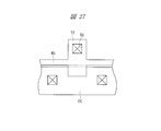
- a pad electrode 51 made of a conductive film in the same layer as the memory gate electrode MG is used for electrical extraction to the outside. That is, the side wall-shaped memory gate electrode MG is formed on the side wall of the selection gate electrode CG by self-alignment, and at the same time, the pad electrode 51 is formed using a photoresist mask in the power supply region (shunt portion) of the memory gate electrode MG. Thereafter, a contact hole 52 reaching the pad electrode 51 is formed in the interlayer insulating film formed on the memory gate electrode MG. The memory gate electrode MG and the conductive film embedded in the contact hole 52 are electrically connected.
- the pad electrode 51 has a shape that rides on the selection gate electrode CG in consideration of an alignment margin between the memory gate electrode MG and the pad electrode 51, a dimensional variation margin, and the like.
- the pad electrode 51 is formed so as to cover the step portion of the selection gate electrode CG, in the photolithography for forming the photoresist mask, a focus shift due to the step occurs, and the processing accuracy of the photoresist mask deteriorates. As a result, a defective shape of the pad electrode 51 may occur.
- the area of the planar shape of the pad electrode 51 should be reduced. It is difficult to reduce the area of the power supply region.
- the thickness of the photoresist applied on the upper surface of the conductive film riding on the selection gate electrode CG is larger than the thickness of the photoresist applied on the upper surface of the conductive film riding on the selection gate electrode CG. getting thin. Therefore, in the dry etching of the conductive film using this photoresist as a mask, the photoresist applied on the upper surface of the conductive film that has run on the selection gate electrode CG is applied to the surface other than the upper surface of the conductive film that has run on the selection gate electrode CG. There is also a problem that the conductive film that has been etched away earlier than the applied photoresist and that has been placed on the select gate electrode CG is scraped, resulting in a defective shape of the pad electrode 51. If a pad electrode having a predetermined shape cannot be obtained, the pad electrode 51 and the plug connected to the pad electrode 51 through the contact hole 52 become high resistance or non-conduction, and the manufacturing yield is lowered.
- An object of the present invention is to provide a technology capable of realizing high integration in a semiconductor device having a nonvolatile memory cell having a split gate structure.
- Another object of the present invention is to provide a technique capable of improving the manufacturing yield in a semiconductor device having a non-volatile memory cell having a split gate structure.
- the semiconductor device is a semiconductor device including a nonvolatile memory cell.
- a nonvolatile memory cell includes a first gate insulating film formed on a semiconductor substrate, a selection gate electrode formed of a first conductive film formed on the first gate insulating film, and a cap formed on the selection gate electrode.
- a contact hole is formed in the interlayer insulating film formed on the cap insulating film and the memory gate electrode, and the plug embedded in the contact hole is connected to the memory gate.
- the semiconductor device is a semiconductor device having memory cells.
- a memory cell includes a first gate insulating film formed on a semiconductor substrate, a selection gate electrode made of a first conductive film formed on the first gate insulating film, and a cap insulating film formed on the selection gate electrode
- a memory gate electrode made of a second conductive film formed in a sidewall shape on one side of the laminated film made of the cap insulating film and the select gate electrode, and a laminated film made of the cap insulating film and the select gate electrode and the memory gate electrode
- a contact hole is formed in the interlayer insulating film formed on the cap insulating film and the drain region in the region where the memory cell is formed. Plug buried in Tohoru is connected to the drain region electrically.
- the method for manufacturing a semiconductor device is a method for manufacturing a semiconductor device including a memory cell.
- the step of forming the memory cell includes (a) a step of forming a first gate insulating film on the semiconductor substrate, (b) a step of forming a first conductive film on the first gate insulating film, and (c) a first step. Forming a second insulating film on the one conductive film; and (d) sequentially processing the second insulating film and the first conductive film, thereby forming a selection gate electrode made of the first conductive film and the selection gate electrode.
- a cap insulating film made of a second insulating film Forming a cap insulating film made of a second insulating film; and (e) forming a second plug for supplying a voltage to the selection gate electrode while leaving the cap insulating film on the selection gate electrode in a region where the memory cell is formed.
- a step of removing the cap insulating film on the selection gate electrode in the region to be formed (f) a step of forming a second gate insulating film on the semiconductor substrate after the step (e); and (g) a second gate.
- step (h) Forming a second conductive film on the insulating film; (h) Forming a memory gate electrode in a sidewall shape on the side surface of the laminated film comprising the cap insulating film and the select gate electrode by performing anisotropic etching on the two conductive films; and (i) the step (h) After the step, in the region where the memory cell is formed, a step of forming a source region and a drain region in the semiconductor substrate, and (j) after the step (i), the upper surface of the memory gate electrode and a cap in the step (e) Forming a silicide layer on the upper surface of the select gate electrode from which the insulating film has been removed, and forming a silicide layer on the upper surfaces of the source region and the drain region.
- the method for manufacturing a semiconductor device is a method for manufacturing a semiconductor device including a memory cell.
- the step of forming the memory cell includes (a) a step of forming a first gate insulating film on the semiconductor substrate, (b) a step of forming a first conductive film on the first gate insulating film, and (c) a first step. Forming a second insulating film on the one conductive film; and (d) sequentially processing the second insulating film and the first conductive film, thereby forming a selection gate electrode made of the first conductive film and the selection gate electrode.
- Forming a gate electrode (h) said (g) process (I) a step of forming a silicide layer on the upper surface of the memory gate electrode, the source region and the drain region after the step (h), and (j) ) A step of forming an interlayer insulating film on the semiconductor substrate, the cap insulating film and the memory gate electrode; (k) a step of forming a contact hole in the interlayer insulating film; and (l) a third conductive film embedded in the contact hole. Forming a third plug connected to the silicide layer on the upper surface of the drain region, and the third plug is also formed on the cap insulating film.
- High integration can be realized in a semiconductor device having a non-volatile memory cell having a split gate structure.
- the manufacturing yield can be improved.
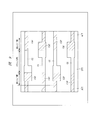
- FIG. 3 is a cross-sectional view of a main part of the nonvolatile memory cell in which the channel of the nonvolatile memory cell according to the first embodiment of the present invention is cut along a direction intersecting the memory gate electrode.
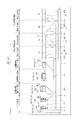
- FIG. 3 is a plan view of a main part of a power feeding region of the nonvolatile memory cell according to Embodiment 1 of the present invention.
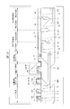
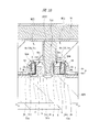
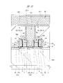
- 2A is a cross-sectional view of the main part taken along the line AA ′ of FIG. 2 (cross-sectional view of the main part of the shunt part of the memory gate electrode), and
- FIG. 2B is taken along the line BB ′ of FIG. It is principal part sectional drawing (essential part sectional drawing of the shunt part of a selection gate electrode).
- FIG. 5 is a plan view of a principal part of a power feeding region in the same manufacturing process as that of FIG. 4 of a semiconductor device having a nonvolatile memory cell.
- FIG. 6 is a main-portion cross-sectional view of the same portion as that in FIG. 4 during the manufacturing process of the semiconductor device having a nonvolatile memory cell, following FIGS. 4 and 5;
- FIG. 7 is a main-portion cross-sectional view of the same portion as that in FIG. 4 during the manufacturing process of the semiconductor device having a non-volatile memory cell following FIG. 6;
- FIG. 6 is a main-portion cross-sectional view of the same portion as that in FIG. 4 during the manufacturing process of the semiconductor device having a non-volatile memory cell following FIG. 6;
- FIG. 6 is a main-portion cross-sectional view of the same portion as that in FIG. 4 during the manufacturing process of the semiconductor device having a non-volatile memory cell following FIG. 6;
- FIG. 6 is a main-
- FIG. 8 is a principal part cross-sectional view of the same place as in FIG. 4 in the process of manufacturing the semiconductor device having a nonvolatile memory cell, following FIG. 7;
- FIG. 8 is a plan view of main parts of the same portions as those in FIG. 5 during the manufacturing process of the semiconductor device having nonvolatile memory cells, following FIG. 7;
- FIG. 10 is an essential part cross-sectional view of the same place as that in FIG. 4 during the manufacturing process of the semiconductor device having a nonvolatile memory cell, following FIG. 8 and FIG. 9;
- FIG. 11 is a principal part cross-sectional view of the same place as in FIG. 4 in the process of manufacturing the semiconductor device having a nonvolatile memory cell, following FIG. 10;
- FIG. 10 is a principal part cross-sectional view of the same place as in FIG. 4 in the process of manufacturing the semiconductor device having a nonvolatile memory cell, following FIG. 10;
- FIG. 10 is a principal part cross-sectional view of the same place as
- FIG. 12 is a principal part cross-sectional view of the same place as in FIG. 4 in the process of manufacturing the semiconductor device having a nonvolatile memory cell, following FIG. 11;
- FIG. 12 is a plan view of main parts of the same portions as those in FIG. 5 during the manufacturing process of the semiconductor device having nonvolatile memory cells, following FIG. 11;
- FIG. 14 is a principal part cross-sectional view of the same place as in FIG. 4 in the process of manufacturing the semiconductor device having a nonvolatile memory cell, following FIG. 12 and FIG. 13;
- FIG. 15 is an essential part cross-sectional view of the same place as that in FIG. 4 during the manufacturing process of the semiconductor device having a nonvolatile memory cell, following FIG. 14;
- FIG. 14 is a principal part cross-sectional view of the same place as that in FIG. 4 during the manufacturing process of the semiconductor device having a nonvolatile memory cell, following FIG. 14;
- FIG. 14 is a principal part cross-sectional view of the same place
- FIG. 16 is a principal part cross-sectional view of the same place as in FIG. 4 in the process of manufacturing the semiconductor device having a nonvolatile memory cell, following FIG. 15;
- FIG. 17 is an essential part cross-sectional view of the same place as that in FIG. 4 during the manufacturing process of the semiconductor device having a nonvolatile memory cell, following FIG. 16;
- FIG. 18 is a principal part cross-sectional view of the same place as in FIG. 4 in the process of manufacturing the semiconductor device having a nonvolatile memory cell, following FIG. 17;
- FIG. 19 is a principal part cross-sectional view of the same place as in FIG. 4 in the process of manufacturing the semiconductor device having a nonvolatile memory cell, following FIG. 18;
- FIG. 18 is a principal part cross-sectional view of the same place as in FIG. 4 in the process of manufacturing the semiconductor device having a nonvolatile memory cell, following FIG. 18;
- FIG. 18 is a principal part cross-sectional view of the same place as in
- FIG. 20 is an essential part cross-sectional view of the same place as that in FIG. 4 during the manufacturing process of the semiconductor device having nonvolatile memory cells, following FIG. 19;
- FIG. 21 is a principal part cross-sectional view of the same place as in FIG. 4 in the process of manufacturing the semiconductor device having a nonvolatile memory cell, following FIG. 20;
- FIG. 22 is a principal part cross-sectional view of the same place as in FIG. 4 in the process of manufacturing the semiconductor device having a nonvolatile memory cell, following FIG. 21;
- FIG. 23 is a principal part cross-sectional view of the same place as in FIG. 4 in the process of manufacturing the semiconductor device having a nonvolatile memory cell, following FIG. 22;
- FIG. 21 is a principal part cross-sectional view of the same place as in FIG. 4 in the process of manufacturing the semiconductor device having a nonvolatile memory cell, following FIG. 20;
- FIG. 22 is a principal part cross-sectional view of the same place as in FIG.
- FIG. 24 is a principal part cross-sectional view of the same place as in FIG. 4 in the process of manufacturing the semiconductor device having a nonvolatile memory cell, following FIG. 23;
- FIG. 25 is a principal part cross-sectional view of the same place as in FIG. 4 in the process of manufacturing the semiconductor device having a nonvolatile memory cell, following FIG. 24;
- FIG. 25 is a main-portion plan view of the same portion as in FIG. 5 in the manufacturing process of the semiconductor device having a non-volatile memory cell following FIG. 24; It is a principal part top view of the electric power feeding area
- FIG. 29 is a principal part cross-sectional view of the same place as in FIG. 28 in the process of manufacturing the semiconductor device having a nonvolatile memory cell, following FIG. 28;
- FIG. 30 is a principal part cross-sectional view of the same place as in FIG. 28 in the process of manufacturing the semiconductor device having a nonvolatile memory cell, following FIG. 29;
- FIG. 31 is a principal part cross-sectional view of the same place as in FIG. 28 in the process of manufacturing the semiconductor device having a nonvolatile memory cell, following FIG. 30;
- FIG. 29 is a principal part cross-sectional view of the same place as in FIG. 28 in the process of manufacturing the semiconductor device having a nonvolatile memory cell, following FIG. 30;
- FIG. 30 is a principal part cross-sectional view of the same place as in FIG. 28 in the process of manufacturing the semiconductor device having a nonvolatile memory cell, following FIG. 30;
- FIG. 29 is a principal part cross-sectional view of the same place as in
- FIG. 31 is a principal part cross-sectional view of the same place as in FIG. 28 in the process of manufacturing the semiconductor device having a nonvolatile memory cell, following FIG. 31;
- FIG. 6 is a cross-sectional view of a main part of a nonvolatile memory cell in which a channel of a nonvolatile memory cell according to a third embodiment of the present invention is cut along a direction intersecting a memory gate electrode.
- It is a principal part top view of the memory area of the non-volatile memory cell by Embodiment 3 of this invention.
- the number of elements when referring to the number of elements (including the number, numerical value, quantity, range, etc.), especially when clearly indicated and when clearly limited to a specific number in principle, etc. Except, it is not limited to the specific number, and may be more or less than the specific number. Further, in the present embodiment, the constituent elements (including element steps and the like) are not necessarily essential unless particularly specified and apparently essential in principle. Yes. Similarly, in the following embodiments, when referring to the shapes, positional relationships, etc. of the components, etc., the shapes are substantially the same unless otherwise specified, or otherwise apparent in principle. And the like are included. The same applies to the above numerical values and ranges.
- a MISFET Metal Insulator Semiconductor Field Effect Transistor
- nMIS n-channel type MISFET
- the MONOS type memory cell described in the following embodiments is also included in the subordinate concept of the MIS.
- silicon nitride, silicon nitride, or silicon nitride not only Si 3 N 4 but also silicon nitride is used and includes an insulating film having a similar composition. .
- the term “wafer” is mainly a Si (Silicon) single crystal wafer. However, not only that, but also an SOI (Silicon On Insulator) wafer and an integrated circuit are formed thereon. Insulating film substrate or the like.
- the shape includes not only a circle or a substantially circle but also a square, a rectangle and the like.
- FIG. 1 is a cross-sectional view of a main part of a nonvolatile memory cell in which a channel is cut along a direction intersecting the memory gate electrode
- FIG. 2 is a plan view of a main part of a power feeding region
- FIGS. 2 is a cross-sectional view of the main part taken along the line AA ′ in FIG.
- a semiconductor substrate 1 is made of, for example, p-type single crystal silicon, and an active region on its main surface (device formation surface) has nMIS (Qnc) for memory cell selection and nMIS (for memory) ( Qnm).
- the drain region Drm of the memory cell MC includes, for example, a relatively low concentration n ⁇ type semiconductor region 2ad and a relatively high concentration n + type semiconductor region having a higher impurity concentration than the n ⁇ type semiconductor region 2ad.
- a semiconductor region 2b (LDD (Lightly Doped Drain) structure).
- the source region Srm of the memory cell MC includes, for example, a relatively low concentration n ⁇ type semiconductor region 2as and a relatively high concentration n + having a higher impurity concentration than the n ⁇ type semiconductor region 2as.
- Type semiconductor region 2b (LDD structure). The n ⁇ type semiconductor regions 2ad and 2as are arranged on the channel region side of the memory cell MC, and the n + type semiconductor region 2b is the n ⁇ type semiconductor regions 2ad and 2as from the channel region side of the memory cell MC. It is located at a distance.
- a selection gate electrode CG of the selection nMIS (Qnc) and a memory gate electrode MG of the memory nMIS (Qnm) are provided on the main surface of the semiconductor substrate 1 between the drain region Drm and the source region Srm.
- the plurality of memory cells MC are adjacent to each other via element isolation portions STI (Shallow Trench Isolation) formed in the semiconductor substrate 1 in the extending direction.
- a cap insulating film CAP is formed on the upper surface of the select gate electrode CG.
- the memory gate electrode MG is formed in a sidewall shape on one side surface of the laminated film including the cap insulating film CAP and the selection gate electrode CG.
- the selection gate electrode CG is made of a first conductive film, for example, n-type low-resistance polycrystalline silicon, and the gate length of the selection gate electrode CG is, for example, about 80 to 120 nm.
- the memory gate electrode MG is made of a second conductive film, for example, n-type low-resistance polycrystalline silicon, and the gate length of the memory gate electrode MG is, for example, about 50 to 100 nm.
- the cap insulating film CAP is made of a second insulating film such as silicon nitride, silicon oxide, silicon oxide containing nitrogen, or silicon carbide containing nitrogen, and has a thickness of about 50 nm, for example.
- the height of the select gate electrode CG from the main surface of the semiconductor substrate 1 is, for example, about 140 nm, and the height of the memory gate electrode MG from the main surface of the semiconductor substrate 1 is the semiconductor substrate 1 of the select gate electrode CG.
- the height is about 50 nm higher than the height from the main surface.
- a silicide layer 3 such as nickel silicide (NiSi) or cobalt silicide (CoSi 2 ) is formed on the upper surface of the memory gate electrode MG.
- the thickness of the silicide layer 3 is, for example, about 20 nm.
- the silicide layer 3 is formed only on the upper surface of the memory gate electrode MG and is not formed on the upper surface of the select gate electrode CG. However, a desired operation speed can be obtained by reducing the resistance of the first conductive film constituting the select gate electrode CG.
- the silicide layer 3 is also formed on the upper surface of the n + type semiconductor region 2b constituting the source region Srm or the drain region Drm.
- a gate insulating film (first gate insulating film) 4 is provided between the select gate electrode CG and the main surface of the semiconductor substrate 1.
- the gate insulating film 4 is made of a first insulating film such as silicon oxide, and has a thickness of about 1 to 5 nm, for example. Accordingly, the selection gate electrode CG is disposed on the element isolation portion and on the first region of the semiconductor substrate 1 with the gate insulating film 4 interposed therebetween.
- boron is introduced to form a p-type semiconductor region 5.
- the semiconductor region 5 is a semiconductor region for forming a channel of the selection nMIS (Qnc), and the threshold voltage of the selection nMIS (Qnc) is set to a predetermined value by the semiconductor region 5.
- the memory gate electrode MG is provided on the side surface of the selection gate electrode CG via a gate insulating film (second gate insulating film).
- This gate insulating film that insulates the selection gate electrode CG and the memory gate electrode MG is a laminated film (hereinafter referred to as an insulating film (fourth insulating film) 6b, a charge storage layer CSL, and an insulating film (fifth insulating film) 6t). Insulating films 6b and 6t and charge storage layer CSL).
- a memory gate electrode MG is disposed on the second region of the semiconductor substrate 1 via the insulating films 6b and 6t and the charge storage layer CSL. In FIG. 1, the notation of the insulating films 6b and 6t and the charge storage layer CSL is expressed as 6b / CSL / 6t.
- the charge storage layer CSL is made of, for example, silicon nitride and has a thickness of, for example, about 5 to 20 nm.
- the insulating films 6b and 6t are made of, for example, silicon oxide, the thickness of the insulating film 6b is, for example, about 1 to 10 nm, and the thickness of the insulating film 6t is, for example, about 4 to 15 nm.
- the insulating films 6b and 6t can be formed of silicon oxide containing nitrogen.
- the sidewall SW is composed of a laminated film including, for example, a silicon oxide film 7b, a silicon nitride film 7m, and a silicon oxide film 7t.
- the thickness of the silicon oxide film 7b is, for example, 20 nm
- the thickness of the silicon nitride film 7m is, for example, 25 nm
- the thickness of the silicon oxide film 7t is, for example, 50 nm.
- the semiconductor region 8 is a semiconductor region for forming a channel of the memory nMIS (Qnm), and the threshold voltage of the memory nMIS (Qnm) is set to a predetermined value by the semiconductor region 8.
- the memory cell MC is covered with an interlayer insulating film 9, and a contact hole (third contact hole) CNT reaching the drain region Drm is formed in the interlayer insulating film 9.
- the interlayer insulating film 9 is made of a third insulating film, and is formed of a laminated film made of, for example, a silicon nitride film 9a and a silicon oxide film 9b.
- a first layer wiring M1 extending in a direction intersecting the memory gate electrode MG (or the selection gate electrode CG) via a plug (third plug) PLG embedded in the contact hole CNT is provided. It is connected.
- the plug PLG is made of a third conductive film, for example, a relatively thin barrier film made of a laminated film of titanium and titanium nitride, and a relatively thick film made of tungsten, aluminum, or the like formed so as to be surrounded by the barrier film. It is comprised by the laminated film which consists of an electrically conductive film.
- the memory gate electrode MG and the selection gate electrode CG are configured as a structure of the shunt portion of the memory gate electrode MG (hereinafter referred to as MG shunt portion) formed in the power feeding region. Except for being formed on the isolation portion STI, the structures of the selection nMIS (Qnc) and the memory nMIS (Qnm) formed in the memory region are almost the same.
- the interlayer insulating film 9 in the power supply region reaches the silicide layer 3 formed on the upper surface of the memory gate electrode MG formed on the side surface of the selection gate electrode CG via the insulating films 6b and 6t and the charge storage layer CSL.
- a contact hole (first contact hole) CM is formed.
- the contact hole CM is formed on the element isolation portion STI, the sidewall SW, the memory gate electrode MG, the insulating films 6b and 6t, and the charge storage layer CSL in the power feeding region. Further, the contact hole CM has a shape that rides on the selection gate electrode CG. Since the cap insulating film CAP is formed on the upper surface of the selection gate electrode CG, the contact hole CM is connected to the selection gate electrode CG. There is no connection. Further, since the contact hole CM is formed on the element isolation portion STI, it is not connected to the semiconductor substrate 1.
- the memory gate electrode MG in the power supply region is connected to a first layer wiring (not shown) through a plug (first plug) PM made of a third conductive film embedded in the contact hole CM.
- the structure of the shunt portion (hereinafter referred to as CG shunt portion) of the selection gate electrode CG formed in the power supply region is the same as that for selection formed in the memory region. It is different from the structure of nMIS (Qnc).
- the cap insulating film CAP is formed on the upper surface of the selection gate electrode CG.
- the cap insulating film is formed on the upper surface of the selection gate electrode CG formed in the power feeding region. No CAP is formed, and a silicide layer 3 is formed on the upper surface of the select gate electrode CG.
- a contact hole (second contact hole) CC reaching the silicide layer 3 formed on the upper surface of the select gate electrode CG is formed in the interlayer insulating film 9 in the power feeding region.
- the selection gate electrode CG in the power supply region is connected to a first layer wiring (not shown) through a plug (second plug) PC made of a third conductive film embedded in the contact hole CC.
- the height of the memory gate MG is formed to be the same as the height of the control gate electrode CG or lower than the height of the control gate electrode CG.
- the gate electrode is formed lower than the height of the control gate electrode CG, the possibility that the silicide layer 3 formed on the memory gate MG and the select gate electrode CG is short-circuited can be reduced.
- the contact hole CM formed in the interlayer insulating film 9 reaches the memory gate electrode MG of the memory nMIS (Qnm) in the power supply region.
- the memory gate electrode MG and the plug PM are electrically connected by burying the plug PM in the contact hole CM. Accordingly, since the formation of the pad electrode 51 shown in FIG. 27 is not necessary, the area of the power supply region can be reduced, and good electrical connection can be made between the memory gate electrode MG and the plug PM. Is obtained. Thereby, the area of the semiconductor device having a nonvolatile memory cell can be reduced. In addition, the manufacturing yield of a semiconductor device having a nonvolatile memory cell can be improved.
- the cap insulating film CAP is formed on the upper surface of the selection gate electrode CG of the selection nMIS (Qnc), the contact hole CM does not reach the selection gate electrode CG. . Therefore, electrical connection between the plug PM embedded in the contact hole CM and the selection gate electrode CG can be prevented.
- the cap insulating film CAP is not formed on the upper surface of the selection gate electrode CG of the selection nMIS (Qnc), and the silicide layer 3 is formed.
- the contact hole CC formed in the interlayer insulating film 9 in the same process as the contact hole CM easily reaches the silicide layer 3 on the upper surface of the selection gate electrode CG, the plug PC embedded in the contact hole CC and Good electrical connection can be obtained with the select gate electrode CG.
- the cap insulating film CAP is formed on the upper surface of the selection gate electrode CG, it is necessary to consider problems such as a short circuit between the memory gate MG and the selection gate electrode CG when the silicide layer 3 is formed. Absent.
- the silicide layer 3 is formed on the selection gate electrode CG in the shunt portion of the selection gate electrode CG.
- the insulating films 6b and 6t and the charge storage layer CSL are formed between the memory gate MG and the control gate electrode CG, there is no particular problem.
- problems such as a short circuit are solved. Therefore, the height of the memory gate MG can be formed lower than the height of the control gate electrode CG.
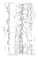
- FIGS. 4, FIG. 6 to FIG. 8, FIG. 10 to FIG. 12 and FIG. 14 to FIG. 25 are a memory region, a power feeding region (MG shunt portion and CG shunt portion), a capacitor element region and a peripheral circuit region in the manufacturing process of the semiconductor device.
- FIG. 5, FIG. 9, FIG. 13, FIG. 26 and FIG. 26 are power supply regions in the manufacturing process of a semiconductor device.
- FIG. 5, FIG. 9, FIG. 13 and FIG. 26 are cross-sectional views of main parts of the low-voltage nMIS region, low-pressure pMIS region, high-voltage nMIS region, and high-voltage pMIS region.
- a main surface of a semiconductor substrate (in this stage, a semiconductor plate having a substantially circular shape called a semiconductor wafer) 1 is surrounded by, for example, a groove-type element isolation portion STI and the same.
- the active regions ACT and the like arranged in this manner are formed. That is, after forming an isolation groove at a predetermined location on the semiconductor substrate 1, an insulating film such as silicon oxide is deposited on the main surface of the semiconductor substrate 1, and the insulating film is left only in the isolation groove.
- the insulating film is polished by a CMP (Chemical-Mechanical-Polishing) method or the like to embed the insulating film in the isolation trench. In this way, the element isolation portion STI is formed.
- This element isolation portion STI is also formed in the semiconductor substrate 1 in the power feeding region and the capacitor element region.
- a buried n-well NISO is formed by selectively ion-implanting n-type impurities into the semiconductor substrate 1 in the peripheral circuit region.
- p-type impurities are selectively ion-implanted into the semiconductor substrate 1 in the memory region and the high-voltage nMIS region to form a p-well HPW, and the n-type impurity is selectively ionized in the semiconductor substrate 1 in the high-voltage pMIS region.
- an n-well HNW is formed.
- n-well NW is formed.
- a p-type impurity such as boron is selectively ion-implanted into the semiconductor substrate 1 in the memory region.
- a p-type semiconductor region 5 for forming a channel for selection nMIS (Qnc) is formed on the semiconductor substrate 1 in the memory region.
- a predetermined impurity is ion-implanted into each semiconductor substrate 1 in the low-voltage nMIS region, the low-voltage pMIS region, the high-voltage nMIS region, and the high-voltage pMIS region in the peripheral circuit region.
- a semiconductor region Dc for channel formation is formed in each semiconductor substrate 1 of the low-voltage nMIS region, the low-voltage pMIS region, the high-voltage nMIS region, and the high-voltage pMIS region in the peripheral circuit region.
- a gate insulating film 4A made of, for example, silicon oxide and having a thickness of about 20 nm is formed on the main surface of the semiconductor substrate 1. Subsequently, after removing the gate insulating film 4A in the memory region, the low-voltage nMIS region, and the low-voltage pMIS region, the semiconductor substrate 1 is subjected to an oxidation process.
- a gate insulating film (first gate insulating film) 4 made of, for example, silicon oxide and having a thickness of about 1 to 5 nm is formed on the main surface of the semiconductor substrate 1 in the memory region, and at the same time, the low-voltage nMIS region and the low-voltage system
- a gate insulating film (third gate insulating film) 4 made of, for example, silicon oxide and having a thickness of about 1 to 5 nm is formed on the main surface of the semiconductor substrate 1 in the pMIS region.
- a conductive film 10 made of, for example, amorphous silicon is deposited on the main surface of the semiconductor substrate 1 by a CVD (Chemical Vapor Deposition) method, and then a memory region, a power supply region, and a capacitor element are deposited.
- An n-type conductive film (first conductive film) 10n is formed by introducing an n-type impurity into the conductive film 10 in the region by an ion implantation method or the like.
- the thickness of the conductive films 10 and 10n is, for example, about 140 nm.
- a cap insulating film CAP is deposited on the conductive films 10 and 10n by a CVD method.
- the cap insulating film CAP is, for example, silicon nitride, silicon oxide, silicon oxide containing nitrogen, or silicon carbide, and has a thickness of, for example, 50 nm.
- the cap insulating film CAP and the n-type conductive film 10n in the memory region, the power feeding region, and the capacitor element region are sequentially patterned by a lithography technique and a dry etching technique.
- the selection gate electrode CG of the selection nMIS (Qnc) made of the n-type conductive film 10n is formed in the memory region and the power supply region.
- the gate length of the selection gate electrode CG in the memory region is, for example, about 100 nm.
- a lower electrode 10E made of an n-type conductive film 10n is formed in the capacitive element region.
- the CG shunt portion in the power feeding region, the capacitor element region, and the cap insulating film CAP in the peripheral circuit region are removed.
- the cap insulating film CAP remaining on the selection gate electrode CG in the power feeding region is indicated by hatching.
- the cap insulating film CAP In the capacitive element region, if the cap insulating film CAP is left, the dielectric film between the lower electrode 10E and the upper electrode formed in a later process becomes too thick, and the capacitance value decreases. Therefore, it is necessary to remove the cap insulating film CAP in the capacitive element region in this step.
- n-type impurities such as arsenic or phosphorus are ion-implanted into the main surface of the semiconductor substrate 1 in the memory region using the cap insulating film CAP, the selection gate electrode CG of the selection nMIS (Qnc) and the resist pattern as a mask.
- the n-type semiconductor region 8 for forming the channel of the memory nMIS (Qnm) is formed.
- an insulating film (fourth insulating film) 6b made of silicon oxide, a charge storage layer CSL made of silicon nitride, and an insulating film made of silicon oxide ( 5th insulating film) 6t is formed sequentially.
- the insulating film 6b is formed by, for example, a thermal oxidation method or an ISSG oxidation method, and the thickness thereof is, for example, about 1 to 10 nm.
- the charge storage layer CSL is formed by a CVD method, and the thickness thereof is, for example, about 5 to 20 nm.
- the insulating film 6t is formed by, for example, a CVD method or an ISSG oxidation method, and the thickness can be exemplified by about 4 to 15 nm, for example.
- the insulating films 6b and 6t may be formed of silicon oxide containing nitrogen.
- a conductive film for forming a memory gate (second conductive film) made of low-resistance polycrystalline silicon is deposited on the main surface of the semiconductor substrate 1.
- This conductive film is formed by the CVD method, and its thickness is, for example, about 50 to 100 nm.
- the conductive film is etched back by an anisotropic dry etching method using a lithography technique and a dry etching technique.
- the insulating films 6b and 6t and the charge storage layer CSL are formed on both side surfaces of the laminated film including the cap insulating film CAP and the selection gate electrode CG of the selection nMIS (Qnc). Sidewalls 11 are formed via two gate insulating films. At the same time, in the CG shunt portion of the power supply region, the sidewalls 11 are formed on both side surfaces of the selection gate electrode CG of the selection nMIS (Qnc) via the insulating films 6b and 6t and the charge storage layer CSL. Further, in the capacitive element region, the upper electrode 11E is formed so as to cover the lower electrode 10E using the resist pattern RP as a mask.
- the sidewall 11 exposed therefrom is etched.
- the memory gate electrode MG of the memory nMIS (Qnm) is formed only on one side surface of the laminated film including the cap insulating film CAP and the selection gate electrode CG of the selection nMIS (Qnc). (Sidewall 11) is formed.
- the gate length of the memory gate electrode MG is, for example, about 65 nm.
- the memory gate electrode MG (sidewall 11) of the memory nMIS (Qnm) is formed only on one side surface of the selection gate electrode CG of the selection nMIS (Qnc) in the CG shunt portion of the power supply region.
- the height of the memory gate electrode MG from the main surface of the semiconductor substrate 1 is higher than the height of the selection gate electrode CG from the main surface of the semiconductor substrate 1 and is the same as the height of the cap insulating film CAP. It is formed lower than that.
- the insulating films 6b and 6t and the charge storage layer CSL are formed between the stacked film including the cap insulating film CAP and the selection gate electrode CG and the memory gate electrode MG, the insulating film The heights of 6b and 6t and the charge storage layer CSL are formed higher than the height of the select gate electrode CG from the main surface of the semiconductor substrate 1.
- the sidewalls 11 are formed on both side surfaces of the laminated film including the cap insulating film CAP and the selection gate electrode CG via the insulating films 6b and 6t and the charge storage layer CSL. Therefore, the height of the memory gate electrode MG from the main surface of the semiconductor substrate 1 is higher than the height of the selection gate electrode CG from the main surface of the semiconductor substrate 1 and is the same as the height of the cap insulating film CAP. It is formed lower than that.
- the insulating films 6b and 6t and the charge storage layer CSL are formed between the stacked film including the cap insulating film CAP and the selection gate electrode CG and the memory gate electrode MG, the insulating film 6b , 6t and the charge storage layer CSL are formed higher than the height of the select gate electrode CG from the main surface of the semiconductor substrate 1.
- the sidewalls 11 are formed on both side surfaces of the selection gate electrode CG via the insulating films 6b and 6t and the charge storage layer CSL.
- the height of the memory gate electrode MG from the main surface of the semiconductor substrate 1 is formed to be substantially equal to or lower than the height of the select gate electrode CG from the main surface of the semiconductor substrate 1.
- the height of the memory gate electrode MG in the CG shunt portion of the power supply region is formed to be lower than the height of the memory gate electrode MG in the memory region from the main surface of the semiconductor substrate 1.
- the insulating films 6b and 6t and the charge storage layer CSL are used as the capacitive insulating film (dielectric film), and the lower electrode 10E made of a conductive film in the same layer as the selection gate electrode CG of the selection nMIS (Qnc); A capacitor element including the memory gate electrode MG of the memory nMIS (Qmc) and the upper electrode 11E made of the same conductive film is formed.
- the capacitive element constitutes a charge pump circuit used in a power supply circuit that outputs a voltage higher than the input voltage, for example.
- the charge pump circuit can increase the voltage by switching the connection state of the plurality of capacitor elements using a switch or the like.
- the capacitive element is formed on the element isolation portion STI formed in the semiconductor substrate 1 and the parasitic capacitance formed by the substrate portion and the lower electrode 10E is negligibly small, the above operation is stably performed. It can be carried out. Further, even if the position of the contact hole reaching the upper electrode 11E and the position of the contact hole reaching the lower electrode 10E formed in a later process is shifted due to the photomask shift or the like, the position shifts on the element isolation portion STI. There is no short circuit between the wiring and the semiconductor substrate 1 through the hole.
- an n-type conductive film 10na is formed by introducing an n-type impurity into the conductive film 10 in the low-voltage nMIS region and the high-voltage nMIS region in the peripheral circuit region by an ion implantation method or the like.
- a p-type conductive film 10p is formed by introducing a p-type impurity into the conductive film 10 in the low-voltage pMIS region and the high-voltage pMIS region in the peripheral circuit region by an ion implantation method or the like.
- the conductive films 10na and 10p in the peripheral circuit region are patterned by the lithography technique and the dry etching technique to form the low-voltage nMIS gate electrode GLn and the conductive film 10p made of the conductive film 10na.
- the gate electrode GLp of the low-voltage pMIS, the gate electrode GHn of the high-voltage nMIS made of the conductive film 10na, and the gate electrode GHp of the high-voltage pMIS made of the conductive film 10p are formed.
- the gate length of the gate electrode GLn of the low voltage system nMIS and the gate electrode GLp of the low voltage system pMIS in the active region is, for example, about 100 nm
- the gate length of the gate electrode GHn of the high voltage system nMIS and the gate electrode GHp of the high voltage system pMIS is, for example, It is about 400 nm.
- an n-type impurity for example, arsenic is ion-implanted into the main surface of the semiconductor substrate 1 using the resist pattern as a mask on the main surface of the semiconductor substrate 1 in the high-voltage nMIS region of the peripheral circuit region, thereby An n ⁇ type semiconductor region 13 is formed on the main surface of the semiconductor substrate 1 in the system nMIS region in a self-aligned manner with respect to the gate electrode GHn.
- a p-type impurity such as boron fluoride is ion-implanted into the main surface of the semiconductor substrate 1 using the resist pattern as a mask on the main surface of the semiconductor substrate 1 in the high-voltage pMIS region of the peripheral circuit region.
- a p ⁇ -type semiconductor region 14 is formed in a self-aligned manner with respect to the gate electrode GHp on the main surface of the semiconductor substrate 1 in the high-voltage pMIS region.
- an insulating film made of, for example, silicon oxide and having a thickness of about 10 nm is deposited on the main surface of the semiconductor substrate 1 by the CVD method, and then the insulating film is anisotropically etched. Etch back. Accordingly, in the memory region and the power supply region, the side surface of the stacked film including the cap insulating film CAP and the selection gate electrode CG on the side opposite to the memory gate electrode MG and the side surface of the memory gate electrode MG, and in the capacitive element region, the upper electrode 11E.
- sidewalls 15 are formed on both side surfaces of the low-voltage nMIS gate electrode GLn, the low-voltage pMIS gate electrode GLp, the high-voltage nMIS gate electrode GHn, and the high-voltage pMIS gate electrode GHp, respectively.
- the spacer length of the sidewall 15 is, for example, about 6 nm.
- the sidewall 15 By forming the sidewall 15, in a step of forming an n ⁇ -type semiconductor region in a low-voltage nMIS region in a peripheral circuit region described later and a step of forming a p ⁇ -type semiconductor region in a low-pressure pMIS region,
- the effective channel length of the n ⁇ -type semiconductor region and the p ⁇ -type semiconductor region can be increased, and the short channel effect of the low-pressure nMIS and the low-pressure pMIS can be suppressed.
- a part of the selection gate electrode CG on the memory gate electrode MG side of the memory nMIS (Qnm) and the memory gate are located at the end of the selection gate electrode CG of the memory region selection nMIS (Qnc).
- an n-type impurity such as arsenic is ion-implanted into the main surface of the semiconductor substrate 1 using the selection gate electrode CG, the memory gate electrode MG, and the resist pattern 16 as a mask.
- An n ⁇ type semiconductor region 2ad is formed on the main surface of 1 in a self-aligned manner with respect to the select gate electrode CG.
- the end of the resist pattern 16 is positioned on the upper surface of the selection gate electrode CG of the memory region selection nMIS (Qnc) and the memory nMIS (Qnm) memory.
- an n-type impurity such as arsenic is used as the semiconductor substrate 1 with the selection gate electrode CG, the memory gate electrode MG, and the resist pattern 17 as a mask.
- an n ⁇ type semiconductor region 2as is formed in the main surface of the semiconductor substrate 1 in a self-aligned manner with respect to the memory gate electrode MG.
- the n ⁇ type semiconductor region 2ad is formed first, and then the n ⁇ type semiconductor region 2as is formed. However, the n ⁇ type semiconductor region 2as is formed first, and then the n ⁇ type semiconductor region 2ad is formed. May be formed. Further, following the ion implantation of the n-type impurity forming the n ⁇ -type semiconductor region 2ad, a p-type impurity, for example, boron is ion-implanted into the main surface of the semiconductor substrate 1, and the lower portion of the n ⁇ -type semiconductor region 2ad is formed. A p-type semiconductor region may be formed so as to surround it.
- n-type impurities such as arsenic are ion-implanted into the main surface of the semiconductor substrate 1 using the resist pattern as a mask on the main surface of the semiconductor substrate 1 in the low-voltage nMIS region in the peripheral circuit region.
- an n ⁇ type semiconductor region 18 is formed in a self-aligned manner with respect to the gate electrode GLn on the main surface of the semiconductor substrate 1 in the low-voltage nMIS region in the peripheral circuit region.
- a p-type impurity such as boron fluoride is ion-implanted into the main surface of the semiconductor substrate 1 using the resist pattern as a mask on the main surface of the semiconductor substrate 1 in the low-voltage pMIS region of the peripheral circuit region.
- a p ⁇ -type semiconductor region 19 is formed in a self-aligned manner with respect to the gate electrode GLp on the main surface of the semiconductor substrate 1 in the low-pressure pMIS region.
- a silicon oxide film 7b, a silicon nitride film 7m, and a silicon oxide film 7t are sequentially deposited on the main surface of the semiconductor substrate 1 by a CVD method, and these are anisotropically dry-etched. Etch back by the method. Accordingly, in the memory region and the power supply region, the side surface of the stacked film including the cap insulating film CAP and the selection gate electrode CG on the side opposite to the memory gate electrode MG and the side surface of the memory gate electrode MG, and in the capacitive element region, the upper electrode 11E.
- sidewalls SW are formed on both side surfaces of the low-voltage nMIS gate electrode GLn, the low-voltage pMIS gate electrode GLp, the high-voltage nMIS gate electrode GHn, and the high-voltage pMIS gate electrode GHp, respectively.
- the thickness of the silicon oxide film 7b is, for example, about 20 nm
- the thickness of the silicon nitride film 7m is, for example, about 25 nm
- the thickness of the silicon oxide film 7t is, for example, about 50 nm.
- a p-type impurity such as boron or boron fluoride is used as a semiconductor on the main surface of the semiconductor substrate 1 in the low-voltage pMIS region and high-voltage pMIS region in the peripheral circuit region, using the resist pattern 20 as a mask.
- a p + -type semiconductor region 21 is formed in a self-aligned manner with respect to the gate electrode GLp of the low-voltage pMIS and the gate electrode GHp of the high-voltage pMIS.
- the source / drain region SD of the high-voltage pMIS composed of the p ⁇ type semiconductor region 14 and the p + type semiconductor region 21 is formed, and the p ⁇ type semiconductor region 19 and the p + type semiconductor region 21 are formed.
- a source / drain region SD of the low-pressure pMIS consisting of is formed.
- n-type impurities such as arsenic and phosphorous are formed on the main surface of the semiconductor substrate 1 in the low-voltage nMIS region and high-voltage nMIS region in the memory region and the peripheral circuit region using the resist pattern 22 as a mask. Is implanted into the main surface of the semiconductor substrate 1 so that the n + -type semiconductor region 2b is applied to the selection gate electrode CG of the selection nMIS (Qnc) and the memory gate electrode MG of the memory nMIS (Qnm) in the memory region.
- an n + type semiconductor region 23 is formed in a self-aligned manner with respect to the gate electrode GLn of the low-voltage nMIS and the gate electrode GHn of the high-voltage nMIS.
- n - -type semiconductor regions 2ad and n + consists -type semiconductor region 2b drain region Drm, n - -type source region Srm comprising a semiconductor region 2as and the n + -type semiconductor region 2b is formed Is done.
- nMIS source / drain region SD composed of an n ⁇ type semiconductor region 13 and an n + type semiconductor region 23 is formed, and the n ⁇ type semiconductor region 18 and the n + type semiconductor region 18 are formed.
- a source / drain region SD of the low-pressure nMIS composed of the semiconductor region 23 is formed.
- the nMIS for memory of the MG shunt portion As shown in FIG. 22, in the memory region, on the upper surface of the memory gate electrode MG of the memory nMIS (Qnm) and the upper surface of the n + -type semiconductor region 2b, in the power supply region, the nMIS for memory of the MG shunt portion.
- a silicide layer 3 is formed by a salicide (Salicide: Self Align silicide) process on the upper surface of a portion that does not overlap the selection gate electrode
- the contact resistance between the silicide layer 3 and a plug or the like formed on the silicide layer 3 can be reduced.
- the resistance of the memory gate electrode MG, the source region Srm, and the drain region Drm of the memory nMIS (Qnm) can be reduced.
- the resistance of the low-voltage nMIS gate electrode GLn, the low-voltage pMIS gate electrode GLp, the high-voltage nMIS gate electrode GHn, and the high-voltage pMIS gate electrode GHp itself or the resistance of the source / drain region SD itself. Can be reduced.
- a silicon nitride film 9a is deposited as an insulating film on the main surface of the semiconductor substrate 1 by a CVD method.
- This silicon nitride film 9a functions as an etching stopper when a contact hole described later is formed.
- a silicon oxide film 9b is deposited as an insulating film by a CVD method to form an interlayer insulating film 9 composed of a silicon nitride film 9a and a silicon oxide film 9b.
- a contact hole (third contact hole) CNT reaching the silicide layer 3 on the drain region Drm is formed in the interlayer insulating film 9.
- a contact hole (second contact hole) CC reaching the silicide layer 3 on the selection gate electrode CG of the selection nMIS (Qnc) of the CG shunt portion is formed, and the memory nMIS (Qnm) of the MG shunt portion is formed.
- the contact hole (first contact hole) CM reaching the silicide layer 3 on the memory gate electrode MG is formed in the interlayer insulating film 9.
- the contact hole CM formed in the MG shunt portion has a shape that rides on the selection gate electrode CG in consideration of an alignment margin between the memory gate electrode MG and the contact hole CM, a dimensional variation margin, and the like. However, since the cap insulating film CAP is formed on the upper surface of the selection gate electrode CG, the contact hole CM is not connected to the selection gate electrode CG.
- the silicide layers 3 on the respective gate electrodes (GHn, GHp, GLn, GLp) and the source / drain regions SD are formed.
- a reaching contact hole CA is formed.
- a contact hole CA reaching the source / drain region SD of the low-voltage nMIS and the low-voltage pMIS is illustrated.
- a contact hole CB reaching the silicide layer 3 on the upper surface of each of the upper electrode 11E and the lower electrode 10E is formed in a portion where the upper electrode 11E and the lower electrode 10E do not overlap in plan view.
- FIG. 25 illustrates a contact hole CB reaching the upper electrode 11E for simplicity of explanation.
- plug PLG third plug in contact hole CNT
- plug PC second plug in contact hole CC
- plug PM first plug in contact hole CM
- plug PA in contact hole CA
- a plug PB is formed in the contact hole CB.
- the plugs PLG, PC, PM, PA, and PB are, for example, a relatively thin barrier film made of a laminated film of titanium and titanium nitride, and a relative film made of tungsten, aluminum, or the like formed so as to be surrounded by the barrier film. And a laminated film made of a thick conductive film.
- a first-layer wiring (not shown) whose main component is, for example, copper or aluminum is formed on the interlayer insulating film 9, thereby forming a low-voltage nMIS formed in the memory cell, the capacitive element, and the peripheral circuit region.
- the low-pressure pMIS, the high-pressure nMIS, and the high-pressure nMIS are almost completed.
- a semiconductor device having a nonvolatile memory is manufactured through a normal manufacturing process of the semiconductor device.
- a thermal oxide film is formed between the select gate electrode CG and the cap insulating film CAP in the MG shunt portion. That is, in the first embodiment described above, the cap insulating film CAP is formed in contact with the selection gate electrode CG of the MG shunt portion.
- the thickness of the select gate electrode CG in the MG shunt portion and the cap insulating film CAP made of, for example, silicon nitride, silicon oxide, silicon oxide containing nitrogen, or silicon carbide is 5 mm, for example.
- a thermal oxide film made of silicon oxide of about ⁇ 10 nm is formed.
- the thermal oxide film is formed by performing a thermal oxidation process on the conductive film 10n constituting the selection gate electrode CG, and the cap insulating film CAP is formed by a CVD method.
- the CAP etching rate can be different from each other. Therefore, when the contact hole CM reaching the silicide layer 3 on the memory gate electrode MG is formed in the interlayer insulating film 9 in the MG shunt portion, the cap insulating film CAP on the selection gate electrode CG is formed by overetching the silicon nitride film 9a.
- this thermal oxide film can function as an etching stopper film, so that the contact hole CM is prevented from reaching the selection gate electrode CG, and the electrical connection between the plug PM in the contact hole CM and the selection gate electrode CG is prevented. Connection can be prevented.
- the cap insulating film CAP is made of silicon nitride
- the cap insulating film CAP and the silicon nitride film 9a are made of silicon nitride, so that cap insulation is further performed by etching when forming the contact hole CM. It is assumed that the film CAP is scraped. However, even in this case, it is possible to obtain a selection ratio between silicon nitride and silicon oxide. Therefore, by forming a thermal oxide film made of silicon oxide on the selection gate electrode CG, overetching can be performed. Even when the cap insulating film CAP on the selection gate electrode CG is scraped, the thermal oxide film effectively works as an etching stopper film.
- FIGS. 28 to 32 show a memory region, a power feeding region (MG shunt portion and CG shunt portion), a capacitor element region and a peripheral circuit region (low-voltage nMIS region, low-voltage pMIS region, and high-voltage nMIS region) during the manufacturing process of the semiconductor device. And a high-pressure system pMIS region).
- the manufacturing process until the gate insulating film 4 is formed on the main surface of the semiconductor substrate 1 in the memory region and the main surface of the semiconductor substrate 1 in the low-pressure nMIS region and the low-pressure pMIS region is the same as that in the first embodiment. Since it is the same, the description is omitted.
- a conductive film 10 made of, for example, amorphous silicon is deposited on the main surface of the semiconductor substrate 1 by the CVD method, and then the conductive film 10 in the memory region, the power feeding region, and the capacitor element region.
- An n-type conductive film 10n is formed by introducing an n-type impurity into the substrate by an ion implantation method or the like.
- a thermal oxide film (sixth insulating film) 25 is formed on the surfaces of the conductive films 10 and 10 n by performing a thermal oxidation process on the semiconductor substrate 1.
- the thermal oxide film 25 is, for example, silicon oxide, and its thickness is, for example, 5 to 10 nm.
- a cap insulating film CAP is deposited on the conductive films 10 and 10n by a CVD method.
- the cap insulating film CAP is, for example, silicon nitride, silicon oxide, silicon oxide containing nitrogen, or silicon carbide, and has a thickness of, for example, 50 nm.
- the cap insulating film CAP, the thermal oxide film 25, and the n-type conductive film 10n in the memory region, the power feeding region, and the capacitive element region are sequentially patterned by lithography technology and dry etching technology.
- the selection gate electrode CG of the selection nMIS (Qnc) made of the n-type conductive film 10n is formed in the memory region and the power supply region.
- a lower electrode 10E made of an n-type conductive film 10n is formed in the capacitive element region.
- the cap insulating film CAP in the CG shunt portion in the power feeding region, the capacitor element region, and the peripheral circuit region is removed.
- the cap insulating film CAP is removed, a part of the thermal oxide film 25 in the CG shunt portion, the capacitive element region, and the peripheral circuit region in the power feeding region is removed.
- the cap insulating film CAP is formed of silicon nitride, it is difficult to obtain a selection ratio in dry etching between the conductive films 10 and 10n made of silicon nitride and amorphous or polycrystalline silicon. Therefore, when removing the cap insulating film CAP, the conductive films 10 and 10n may also be etched.
- the thermal oxide film 25 is formed on the conductive films 10 and 10n, and the silicon nitride and the silicon oxide can obtain a selection ratio at the time of dry etching.
- the thermal oxide film 25 functions as an etching stopper film when etching the cap insulating film CAP.
- n-type impurities such as arsenic or phosphorus are ion-implanted into the main surface of the semiconductor substrate 1 in the memory region using the cap insulating film CAP, the selection gate electrode CG of the selection nMIS (Qnc) and the resist pattern as a mask.
- the n-type semiconductor region 8 for forming the channel of the memory nMIS (Qnm) is formed.
- the thermal oxide film 25 remaining in the CG shunt portion, the capacitive element region, and the peripheral circuit region in the power feeding region is completely removed.
- the thermal oxide film 25 in the peripheral circuit region it is necessary to form the silicide layer 3 on the gate electrodes of the low-voltage nMIS, the low-voltage pMIS, the high-voltage nMISS, and the high-voltage pMIS that will be formed later. Therefore, it is necessary to remove the thermal oxide film 25 in the peripheral circuit region in this step.
- the thermal oxide film 25 is left in the capacitive element region, the dielectric film between the lower electrode 10E and the upper electrode formed in a later process becomes too thick, and the capacitance value decreases. Therefore, it is necessary to remove the thermal oxide film 25 in the capacitive element region in this step.
- an insulating film 6b made of, for example, silicon oxide, a charge storage layer CSL made of silicon nitride, and an insulating film 6t made of silicon oxide are sequentially formed on the main surface of the semiconductor substrate 1, and then the MGs in the memory region and the power feeding region are formed.
- sidewalls 11 are formed on both side surfaces of the laminated film including the cap insulating film CAP and the selection gate electrode CG of the selection nMIS (Qnc) via the insulating films 6b and 6t and the charge storage layer CSL.
- the sidewalls 11 are formed on both side surfaces of the selection gate electrode CG of the selection nMIS (Qnc) via the insulating films 6b and 6t and the charge storage layer CSL. Further, in the capacitive element region, the upper electrode 11E is formed so as to cover the lower electrode 10E using the resist pattern RP as a mask.
- the cap insulating film CAP and the selection gate electrode of the selection nMIS (Qnc)
- a memory gate electrode MG (sidewall 11) of a memory nMIS (Qnm) is formed only on one side surface of the laminated film made of CG, and at the same time, a selection gate electrode of a selection nMIS (Qnc) in the CG shunt portion of the power supply region
- a memory gate electrode MG (sidewall 11) of a memory nMIS (Qnm) is formed only on one side of the CG.
- the conductive film 10 in the low-voltage nMIS region and the high-voltage nMIS region in the peripheral circuit region is changed to the n-type conductive film 10na.
- the conductive films 10na and 10p in the peripheral circuit region are patterned by a lithography technique and a dry etching technique.
- An electrode GHp is formed.
- the drain region Drm, n consisting of the n ⁇ type semiconductor region 2ad and the n + type semiconductor region 2b
- a source region Srm including a ⁇ type semiconductor region 2 as and an n + type semiconductor region 2 b is formed, and a high-voltage nMIS including an n ⁇ type semiconductor region 13 and an n + type semiconductor region 23 is formed in the peripheral circuit region.
- a source / drain region SD is formed, and a source / drain region SD of a low-voltage nMIS composed of an n ⁇ type semiconductor region 18 and an n + type semiconductor region 23 is formed.
- the silicide layer 3 is formed in a predetermined region.
- a silicon nitride film 9a is deposited as an insulating film on the main surface of the semiconductor substrate 1 by the CVD method according to the same manufacturing process as that of the first embodiment (see FIGS. 23 and 24).
- This silicon nitride film 9a functions as an etching stopper when a contact hole described later is formed.
- a silicon oxide film 9b is deposited as an insulating film by a CVD method to form an interlayer insulating film 9 composed of a silicon nitride film 9a and a silicon oxide film 9b.
- the silicon oxide film 9b and the silicon nitride film 9a are sequentially etched by the lithography technique and the dry etching technique, and in the memory region, the contact hole CNT reaching the silicide layer 3 on the drain region Drm. Is formed in the interlayer insulating film 9.
- a contact hole CC reaching the silicide layer 3 on the selection gate electrode CG of the selection nMIS (Qnc) in the CG shunt portion is formed, and the memory gate electrode MG of the memory nMIS (Qnm) in the MG shunt portion.
- a contact hole CM reaching the upper silicide layer 3 is formed in the interlayer insulating film 9.
- the contact hole CM formed in the MG shunt portion has a shape that rides on the selection gate electrode CG in consideration of an alignment margin and a dimensional variation margin between the memory gate electrode MG and the contact hole CM.
- the cap insulating film CAP is formed on the upper surface of the selection gate electrode CG, the contact hole CM is not connected to the selection gate electrode CG.
- the silicon oxide film 9b and the silicon nitride film 9a constituting the interlayer insulating film 9 are sequentially etched, so that the cap insulating film CAP is etched when the silicon nitride film 9a is overetched. It is also possible.
- the thermal oxide film 25 that functions as an etching stopper film of the cap insulating film CAP is formed between the selection gate part CG of the MG shunt part and the cap insulating film CAP, the contact hole CM is formed of the selection gate electrode. There is no connection with the CG.
- the silicide layers 3 on the gate electrodes (GHn, GHp, GLn, GLp) and the source / drain regions SD are formed.
- a reaching contact hole CA is formed.
- FIG. 32 illustrates a contact hole CA reaching the source / drain region SD of the low-voltage nMIS and the low-voltage pMIS for simplification of description.
- a contact hole CB reaching the silicide layer 3 on the upper surface of each of the upper electrode 11E and the lower electrode 10E is formed in a portion where the upper electrode 11E and the lower electrode 10E do not overlap in plan view.
- FIG. 32 illustrates a contact hole CB reaching the upper electrode 11E for the sake of simplicity.
- plug PLG third plug in contact hole CNT
- plug PC second plug in contact hole CC
- plug PM first plug in contact hole CM
- plug PA in contact hole CA
- a plug PB is formed in the contact hole CB.
- a first-layer wiring (not shown) whose main component is, for example, copper or aluminum is formed on the interlayer insulating film 9, thereby forming a low-voltage nMIS formed in the memory cell, the capacitive element, and the peripheral circuit region.
- the low-pressure pMIS, the high-pressure nMIS, and the high-pressure nMIS are almost completed.
- a semiconductor device having a nonvolatile memory is manufactured through a normal manufacturing process of the semiconductor device.
- FIG. 33 is a fragmentary cross-sectional view of a nonvolatile memory cell in which the channel is cut along the direction intersecting the memory gate electrode
- FIG. 34 is a fragmentary plan view of the memory region.
- the memory cell MC2 is covered with an interlayer insulating film 9.
- the interlayer insulating film 9 is made of a third insulating film, and is composed of a laminated film made of, for example, a silicon nitride film 9a and a silicon oxide film 9b.
- a contact hole (fourth contact hole) CNTS reaching the drain region Drm is formed in the interlayer insulating film 9.
- the diameter of the contact hole CNTS formed in the interlayer insulating film 9 is larger than the distance between the adjacent select gate electrodes CG across the drain region Drm.
- the contact hole CNTS has a shape that rides on each of the adjacent selection gate electrodes CG. Therefore, for example, compared with the memory cell (memory cell in which the contact hole CNT does not run on the selection gate electrode CG) MC shown in the first embodiment, the memory cell (on the selection gate electrode CG) shown in the third embodiment.
- the memory cell MC2 which has the contact hole CNTS over the drain region Drm does not have to consider the alignment margin between the drain region Drm and the contact hole CNTS, the distance between the adjacent select gate electrodes CG across the drain region Drm Can be shortened. Thereby, the cell size of the memory cell MC2 can be reduced. Since the cap insulating film CAP is formed on the upper surface of the selection gate electrode CG, the contact hole CNTS is similar to the contact hole CM formed in the MG shunt portion of the first embodiment described above. There is no connection with the CG.
- the width of the sidewall SW is 50 nm and the contact hole CNT is connected to the drain region Drm. Is 80 nm, and the alignment margin between the drain region Drm and the contact hole CNTS is ⁇ 30 nm, the distance between the adjacent select gate electrodes CG across the drain region Drm is required to be 240 nm.
- the position of the drain region Drm and the contact hole CNTS is assumed when the width of the sidewall SW is 50 nm.
- the length in the cross-sectional direction shown in FIG. 33 of the portion where the contact hole CNTS is connected to the drain region Drm can be reduced to, for example, 50 nm, and the drain region Drm can be reduced.
- the distance between the select gate electrodes CG adjacent to each other can be set to 150 nm.
- FIG. 35 shows a first modification of the contact hole CNTS according to the third embodiment.
- FIG. 35 is a cross-sectional view of the main portion at the same position as the cross-sectional view of the main portion shown in FIG.
- the contact hole CNTS runs over the cap insulating film CAP formed on the upper surface of each select gate electrode CG of each of the two adjacent memory cells MC2 across the drain region Drm.
- one of the contact holes CNTS is formed on the upper surface of one of the select gate electrodes CG of two memory cells MC2 adjacent to each other with the drain region Drm interposed therebetween. It rides on the cap insulating film CAP. In this way, even if the contact hole CNTS has a shape that only runs on one side of the selection gate electrode CG, the other of the contact holes CNTS runs on the sidewall SW. There is no connection with the CG.
- FIG. 36 shows a second modification of the contact hole CNTS according to the third embodiment.
- 36 is a plan view of relevant parts of the same portions as the plan view of relevant parts shown in FIG. 34 described above.
- a rectangular contact hole CNTS is designed, and the planar shape of the actually formed contact hole CNTS is an ellipse.
- a square contact hole CNTS is designed, and the planar shape of the contact hole CNTS actually formed is a perfect circle. Thereby, the interval between the adjacent select gate electrodes CG can be further reduced.
- FIG. 37 shows a third modification of the contact hole CNTS according to the third embodiment.
- FIG. 37 is a fragmentary cross-sectional view of the same portion as the principal cross-sectional view shown in FIG.
- the cap insulating film CAP is formed in contact with the selection gate electrode CG.
- the thermal oxide film 25 is formed between the select gate electrode CG and the cap insulating film CAP.
- the thermal oxide film 25 is made of, for example, silicon oxide having a thickness of about 5 to 10 nm, and the etching rate of the thermal oxide film and the etching rate of the cap insulating film CAP can be different from each other.
- the contact hole CNTS is formed in the interlayer insulating film 9 composed of the laminated film of the silicon nitride film 9a and the silicon oxide film 9b, even if the cap insulating film CAP is scraped by overetching of the silicon nitride film 9a, this heat Since the oxide film 25 can function as an etching stopper film, the contact hole CNTS is prevented from reaching the selection gate electrode CG, and electrical connection between the plug PLG in the contact hole CNTS and the selection gate electrode CG is prevented. be able to.
- the present invention can be used for a semiconductor device having a semiconductor element including a first gate electrode and a second gate electrode which are formed adjacent to each other through an insulating film.
- the present invention can be used for a semiconductor device having a memory cell having a split gate structure with a two-transistor structure.
Landscapes
- Semiconductor Memories (AREA)
- Non-Volatile Memory (AREA)
Abstract
Description
本発明の実施の形態1による不揮発性メモリセルの構造の一例を図1によって説明し、不揮発性メモリセルを構成するメモリゲート電極および選択ゲート電極の給電領域の構造の一例を図2および図3によって説明する。図1はチャネルをメモリゲート電極に対して交差する方向に沿って切断した不揮発性メモリセルの要部断面図、図2は給電領域の要部平面図、図3(a)および(b)はそれぞれ図2のA-A′線に沿った要部断面図(メモリゲート電極のシャント部の要部断面図)および図2のB-B′線に沿った要部断面図(選択ゲート電極のシャント部の要部断面図)である。ここでは、サイドウォール形状のメモリゲート電極を採用したスプリットゲート構造のMONOS型不揮発性メモリセルを例示している。
前述の実施の形態1と相違する点は、MGシャント部の選択ゲート電極CGとキャップ絶縁膜CAPとの間に熱酸化膜が形成されていることである。すなわち、前述した実施の形態1では、MGシャント部の選択ゲート電極CGに接してキャップ絶縁膜CAPが形成されている。しかし、本実施の形態2では、MGシャント部の選択ゲート電極CGと、例えば窒化シリコン、酸化シリコン、窒素を含んだ酸化シリコン、炭化シリコンからなるキャップ絶縁膜CAPとの間に、例えば厚さ5~10nm程度の酸化シリコンからなる熱酸化膜が形成されている。熱酸化膜は選択ゲート電極CGを構成する導電膜10nに対して熱酸化処理を施すことにより形成され、キャップ絶縁膜CAPはCVD法により形成されるので、熱酸化膜のエッチング速度とキャップ絶縁膜CAPのエッチング速度とを互いに異なる値とすることができる。従って、MGシャント部においてメモリゲート電極MG上のシリサイド層3に達するコンタクトホールCMを層間絶縁膜9に形成する際に、窒化シリコン膜9aのオーバーエッチングにより選択ゲート電極CG上のキャップ絶縁膜CAPが削れても、この熱酸化膜をエッチングストッパ膜として機能させることができるので、コンタクトホールCMが選択ゲート電極CGに達するのを防いで、コンタクトホールCM内のプラグPMと選択ゲート電極CGとの電気的な接続を防ぐことができる。
前述の実施の形態1と相違する点は、メモリ領域のドレイン領域Drm上のシリサイド層3に達するコンタクトホールCNTが、選択ゲート電極CGの上面に形成されたキャップ絶縁膜CAP上に乗り上げた形状となっていることである。
Claims (59)
- メモリセルを有する半導体装置であって、前記メモリセルは、
半導体基板上に形成された第1絶縁膜からなる第1ゲート絶縁膜と、
前記第1ゲート絶縁膜上に形成された第1導電膜からなる選択ゲート電極と、
前記選択ゲート電極上に形成された第2絶縁膜からなるキャップ絶縁膜と、
前記キャップ絶縁膜および前記選択ゲート電極からなる積層膜の片側面にサイドウォール状に形成された第2導電膜からなるメモリゲート電極と、
前記キャップ絶縁膜および前記選択ゲート電極からなる前記積層膜と前記メモリゲート電極との間に形成され、かつ、前記メモリゲート電極と前記半導体基板との間に形成された第2ゲート絶縁膜とを有し、
前記メモリゲート電極に電圧を供給する第1プラグが形成された領域では、前記半導体基板、前記キャップ絶縁膜および前記メモリゲート電極上に第3絶縁膜からなる層間絶縁膜があり、前記層間絶縁膜に形成された第1コンタクトホールに第3導電膜を埋め込んで形成された前記第1プラグは、前記メモリゲート電極と電気的に接続し、かつ、前記キャップ絶縁膜の一部を覆うように形成されていることを特徴とする半導体装置。 - 請求項1に記載の半導体装置において、前記キャップ絶縁膜は、窒化シリコン、酸化シリコン、窒素を含んだ酸化シリコンまたは炭化シリコンであることを特徴とする半導体装置。
- 請求項1に記載の半導体装置において、前記第2ゲート絶縁膜は、第4絶縁膜、前記第4絶縁膜上に形成された電荷蓄積層および前記電荷蓄積層上に形成された第5絶縁膜からなる積層膜によって形成されていることを特徴とする半導体装置。
- 請求項3に記載の半導体装置において、前記電荷蓄積層は、窒化シリコンであることを特徴とする半導体装置。
- 請求項1に記載の半導体装置において、前記メモリセルの周辺にはMISFETが形成されており、前記MISFETは、
前記半導体基板上に形成された前記第1絶縁膜からなる第3ゲート絶縁膜と、
前記第3ゲート絶縁膜上に形成され、前記第1導電膜からなるゲート電極とを有することを特徴とする半導体装置。 - 請求項1に記載の半導体装置において、前記選択ゲート電極に電圧を供給する第2プラグが形成された領域では、前記キャップ絶縁膜は除去されており、前記層間絶縁膜に形成された第2コンタクトホールに前記第3導電膜を埋め込んで形成された前記第2プラグは、前記選択ゲート電極の上面に形成されたシリサイド層と電気的に接続していることを特徴とする半導体装置。
- 請求項1に記載の半導体装置において、前記メモリセルが形成された領域では、前記選択ゲート電極の前記半導体基板の主面からの高さは、前記メモリゲート電極の前記半導体基板の主面からの高さよりも低いことを特徴とする半導体装置。
- 請求項1に記載の半導体装置において、前記メモリセルが形成された領域および前記メモリゲート電極に電圧を供給する前記第1プラグが形成された領域における前記メモリゲート電極の前記半導体基板の主面からの高さは、前記選択ゲート電極に電圧を供給する前記第2プラグが形成された領域における前記メモリゲート電極の前記半導体基板の主面からの高さよりも高いことを特徴とする半導体装置。
- 請求項1に記載の半導体装置において、前記メモリゲート電極に電圧を供給する前記第1プラグが形成された領域および前記選択ゲート電極に電圧を供給する前記第2プラグが形成された領域では、前記半導体基板に絶縁膜からなる素子分離部が形成されていることを特徴とする半導体装置。
- 請求項1に記載の半導体装置において、さらに、前記メモリセルは、前記選択ゲート電極の前記メモリゲート電極と反対側の前記半導体基板にドレイン領域を有し、
前記メモリセルが形成された領域では、前記半導体基板、前記キャップ絶縁膜および前記メモリゲート電極上に前記第3絶縁膜からなる前記層間絶縁膜があり、前記層間絶縁膜に形成された第3コンタクトホールに前記第3導電膜を埋め込んで形成された第3プラグは、前記ドレイン領域と電気的に接続しており、
前記第3プラグは、前記キャップ絶縁膜上にも形成されていることを特徴とする半導体装置。 - 請求項10に記載の半導体装置において、前記ドレイン領域を共有して2つの前記メモリセルがチャネル方向に対称的に配置されており、
前記第3プラグは、前記2つのメモリセルのそれぞれの前記キャップ絶縁膜上に形成されていることを特徴とする半導体装置。 - 請求項10に記載の半導体装置において、前記第3コンタクトホールは平面形状が楕円形または真円であることを特徴とする半導体装置。
- 請求項10に記載の半導体装置において、前記ドレイン領域上にはシリサイド層が形成され、前記第3プラグは前記シリサイド層と接続していることを特徴とする半導体装置。
- 請求項1に記載の半導体装置において、前記メモリセルが形成された領域および前記メモリゲート電極に電圧を供給する前記第1プラグが形成された領域では、前記選択ゲート電極と前記キャップ絶縁膜との間に、第6絶縁膜からなる熱酸化膜が形成されていることを特徴とする半導体装置。
- 請求項14に記載の半導体装置において、前記第6絶縁膜は酸化シリコンであることを特徴とする半導体装置。
- メモリセルおよび容量素子を有する半導体装置において、
前記メモリセルは、
半導体基板上に形成された第1絶縁膜からなる第1ゲート絶縁膜と、
前記第1ゲート絶縁膜上に形成された第1導電膜からなる選択ゲート電極と、
前記選択ゲート電極上に形成された第2絶縁膜からなるキャップ絶縁膜と、
前記キャップ絶縁膜および前記選択ゲート電極からなる積層膜の片側面にサイドウォール状に形成された第2導電膜からなるメモリゲート電極と、
前記キャップ絶縁膜および前記選択ゲート電極からなる前記積層膜と前記メモリゲート電極との間に形成され、かつ、前記メモリゲート電極と前記半導体基板との間に形成された第2ゲート絶縁膜とを有し、
前記容量素子は、
前記第1導電膜からなる下部電極と、
前記下部電極上に形成され、前記第2ゲート絶縁膜と同一層の膜である誘電体膜と、
前記誘電体膜上に形成された前記第2導電膜からなる上部電極とを有し、
前記容量素子は前記キャップ絶縁膜を有していないことを特徴とする半導体装置。 - 請求項16に記載の半導体装置において、前記容量素子は、チャージポンプ回路に用いられることを特徴とする半導体装置。
- 請求項16に記載の半導体装置において、前記メモリゲート電極に電圧を供給する第1プラグが形成された領域では、前記半導体基板、前記キャップ絶縁膜および前記メモリゲート電極上に第3絶縁膜からなる層間絶縁膜があり、前記層間絶縁膜に形成された第1コンタクトホールに第3導電膜を埋め込んで形成された第1プラグは、前記メモリゲート電極と電気的に接続していることを特徴とする半導体装置。
- 請求項16に記載の半導体装置において、前記キャップ絶縁膜は窒化シリコン、酸化シリコン、窒素を含んだ酸化シリコンまたは炭化シリコンであることを特徴とする半導体装置。
- 請求項16に記載の半導体装置において、前記第2ゲート絶縁膜は、第4絶縁膜、前記第4絶縁膜上に形成された電荷蓄積層および前記電荷蓄積層上に形成された第5絶縁膜からなる積層膜によって形成されていることを特徴とする半導体装置。
- 請求項20に記載の半導体装置において、前記電荷蓄積層は、窒化シリコンであることを特徴とする半導体装置。
- 請求項16に記載の半導体装置において、前記メモリセルおよび容量素子が形成された領域の周辺には、MISFETが形成されており、前記MISFETは、
前記半導体基板上に形成された前記第1絶縁膜からなる第3ゲート絶縁膜と、
前記第3ゲート絶縁膜上に形成され、前記第1導電膜からなるゲート電極とを有することを特徴とする半導体装置。 - 請求項16に記載の半導体装置において、前記選択ゲート電極に電圧を供給する第2プラグが形成された領域では、前記キャップ絶縁膜は除去されおり、前記層間絶縁膜に形成された第2コンタクトホールに前記第3導電膜を埋め込んで形成された前記第2プラグは、前記選択ゲートの上面に形成されたシリサイド層と電気的に接続していることを特徴とする半導体装置。
- 請求項16に記載の半導体装置において、前記メモリセルが形成された領域では、前記選択ゲート電極の前記半導体基板の主面からの高さは、前記メモリゲート電極の前記半導体基板の主面からの高さよりも低いことを特徴とする半導体装置。
- 請求項16に記載の半導体装置において、前記メモリセルが形成された領域および前記メモリゲート電極に電圧を供給する前記第1プラグが形成された領域における前記メモリゲート電極の前記半導体基板の主面からの高さは、前記選択ゲート電極に電圧を供給する第2プラグが形成された領域における前記メモリゲート電極の前記半導体基板の主面からの高さよりも高いことを特徴とする半導体装置。
- 請求項16に記載の半導体装置において、前記メモリゲート電極に電圧を供給する前記第1プラグが形成された領域および前記選択ゲート電極に電圧を供給する前記第2プラグが形成された領域では、前記半導体基板に絶縁膜からなる素子分離部が形成されていることを特徴とする半導体装置。
- 請求項18に記載の半導体装置において、前記メモリセルが形成された領域および前記メモリゲート電極に電圧を供給する前記第1プラグが形成された領域では、前記選択ゲート電極と前記キャップ絶縁膜との間に、第6絶縁膜からなる熱酸化膜が形成されていることを特徴とする半導体装置。
- 請求項27に記載の半導体装置において、前記第6絶縁膜は酸化シリコンであることを特徴とする半導体装置。
- メモリセルを有する半導体装置であって、前記メモリセルは、
半導体基板上に形成された第1絶縁膜からなる第1ゲート絶縁膜と、
前記第1ゲート絶縁膜上に形成された第1導電膜からなる選択ゲート電極と、
前記選択ゲート電極上に形成された第2絶縁膜からなるキャップ絶縁膜と、
前記キャップ絶縁膜および前記選択ゲート電極からなる積層膜の片側面にサイドウォール状に形成された第2導電膜からなるメモリゲート電極と、
前記キャップ絶縁膜および前記選択ゲート電極からなる前記積層膜と前記メモリゲート電極との間に形成され、かつ、前記メモリゲート電極と前記半導体基板との間に形成された第2ゲート絶縁膜と、
前記選択ゲート電極の前記メモリゲート電極と反対側の前記半導体基板にドレイン領域とを有し、
前記メモリセルが形成された領域では、前記半導体基板、前記キャップ絶縁膜および前記メモリゲート電極上に第3絶縁膜からなる層間絶縁膜があり、前記層間絶縁膜に形成された第4コンタクトホールに第3導電膜を埋め込んで形成された第3プラグは、前記ドレイン領域と電気的に接続しており、
前記第3プラグは、前記キャップ絶縁膜上にも形成されていることを特徴とする半導体装置。 - 請求項29に記載の半導体装置において、前記ドレイン領域を共有して2つのメモリセルがチャネル方向に対称的に配置されており、
前記第3プラグは、前記2つのメモリセルのそれぞれの前記キャップ絶縁膜上に形成されていることを特徴とする半導体装置。 - 請求項29に記載の半導体装置において、前記第4コンタクトホールは平面形状が楕円形または真円であることを特徴とする半導体装置。
- 請求項29に記載の半導体装置において、前記ドレイン領域上にはシリサイド層が形成され、前記第3プラグは前記シリサイド層と接続していることを特徴とする半導体装置。
- 請求項29に記載の半導体装置において、前記選択ゲート電極と前記キャップ絶縁膜との間には、第6絶縁膜からなる熱酸化膜が形成されていることを特徴とする半導体装置。
- 請求項33に記載の半導体装置において、前記第6絶縁膜は酸化シリコンであることを特徴とする半導体装置。
- 第1メモリセルを有する半導体装置の製造方法であって、前記第1メモリセルを形成する工程は、
(a)半導体基板上に第1絶縁膜を堆積して、第1ゲート絶縁膜を形成する工程と、
(b)前記第1ゲート絶縁膜上に第1導電膜を形成する工程と、
(c)前記第1導電膜上に第2絶縁膜を形成する工程と、
(d)前記第2絶縁膜および前記第1導電膜を加工することによって、前記第1導電膜からなる選択ゲート電極と、前記選択ゲート電極上に前記第2絶縁膜からなるキャップ絶縁膜とを形成する工程と、
(e)前記第1メモリセルが形成される領域の前記選択ゲート電極上の前記キャップ絶縁膜は残し、前記選択ゲート電極に電圧を供給する第2プラグが形成される領域の前記選択ゲート電極上の前記キャップ絶縁膜は除去する工程と、
(f)前記(e)工程の後に、前記半導体基板上に第2ゲート絶縁膜を形成する工程と、
(g)前記第2ゲート絶縁膜上に第2導電膜を形成する工程と、
(h)前記第2導電膜に対して異方性エッチングを施すことによって、前記キャップ絶縁膜および前記選択ゲート電極からなる積層膜の側面にサイドウォール状にメモリゲート電極を形成する工程と、
(i)前記(h)工程の後に、前記第1メモリセルが形成される領域では、前記半導体基板に第1ソース領域および第1ドレイン領域を形成する工程と、
(j)前記(i)工程の後に、前記メモリゲート電極の上面、前記選択ゲート電極に電圧を供給する前記第2プラグが形成される領域の前記選択ゲート電極の上面、ならびに前記第1メモリセルが形成される領域の前記第1ソース領域および第1ドレイン領域の上面にシリサイド層を形成する工程と、
を含むことを特徴とする半導体装置の製造方法。 - 請求項35に記載の半導体装置の製造方法において、前記選択ゲート電極に電圧を供給する前記第2プラグが形成される領域では、
前記半導体基板、前記選択ゲート電極および前記メモリゲート電極上に層間絶縁膜を形成する工程と、
前記層間絶縁膜に第2コンタクトホールを形成する工程と、
前記第2コンタクトホール内に前記第3導電膜を埋め込み、前記第2プラグを形成する工程と、
を含み、前記第2プラグは前記選択ゲート電極の上面の前記シリサイド層と接続していることを特徴とする半導体装置の製造方法。 - 請求項35に記載の半導体装置の製造方法において、前記メモリゲート電極に電圧を供給する第1プラグが形成される領域では、
前記(e)工程において、前記選択ゲート電極上の前記キャップ絶縁膜を残す工程と、
前記半導体基板、前記選択ゲート電極および前記メモリゲート電極上に層間絶縁膜を形成する工程と、
前記層間絶縁膜に第1コンタクトホールを形成する工程と、
前記第1コンタクトホール内に第3導電膜を埋め込み、第1プラグを形成する工程と、
を含み、前記第1プラグは前記メモリゲート電極の上面の前記シリサイド層と接続し、かつ、前記キャップ絶縁膜の一部を覆うように形成されていることを特徴とする半導体装置の製造方法。 - 請求項35に記載の半導体装置の製造方法において、前記(f)工程における前記第2ゲート絶縁膜を形成する工程は、
前記(e)工程の後に、前記半導体基板上に第4絶縁膜を形成する工程と、
前記第4絶縁膜上に電荷蓄積層を形成する工程と、
前記電荷蓄積層上に第5絶縁膜を形成する工程と、
を含むことを特徴とする半導体装置の製造方法。 - 請求項35に記載の半導体装置の製造方法において、前記メモリゲート電極に電圧を供給する前記第1プラグが形成される領域および前記選択ゲート電極に電圧を供給する前記第2プラグが形成される領域には、前記半導体基板に絶縁膜からなる素子分離部が形成されていることを特徴とする半導体装置の製造方法。
- 半導体基板上に第1メモリセルおよび前記第1メモリセルの周辺に形成されるMISFETを有する半導体装置の製造方法であって、前記第1メモリセルおよび前記MISFETを形成する工程は、
(a)前記半導体基板上に第1絶縁膜を堆積し、前記第1メモリセルの第1ゲート絶縁膜および前記MISFETの第3ゲート絶縁膜を形成する工程と、
(b)前記第1ゲート絶縁膜上および第3ゲート絶縁膜上に第1導電膜を形成する工程と、
(c)前記第1導電膜上に第2絶縁膜を形成する工程と、
(d)前記第1メモリセルが形成される領域の前記第2絶縁膜および前記第1導電膜を加工することによって、前記第1導電膜からなる前記第1メモリセルの選択ゲート電極と、前記選択ゲート電極上に前記第2絶縁膜からなるキャップ絶縁膜とを形成する工程と、
(e)前記第1メモリセルが形成される領域の前記選択ゲート電極上の前記キャップ絶縁膜は残し、前記MISFETが形成される領域の前記第2絶縁膜は除去する工程と、
(f)前記(e)工程の後に、前記半導体基板上に第2ゲート絶縁膜を形成する工程と、
(g)前記第2ゲート絶縁膜上に第2導電膜を形成する工程と、
(h)前記第2導電膜に対して異方性エッチングを施すことによって、前記第1メモリセルの前記キャップ絶縁膜および前記選択ゲート電極からなる積層膜の側面にサイドウォール状にメモリゲート電極を形成する工程と、
(i)前記MISFETが形成される領域の前記第1導電膜を加工することによって、前記MISFETのゲート電極を形成する工程と、
(j)前記(i)工程の後に、前記第1メモリセルが形成される領域では、前記半導体基板に第1ソース領域および第1ドレイン領域を形成し、前記MISFETが形成される領域では、前記半導体基板に第2ソース領域および第2ドレイン領域を形成する工程と、
(k)前記(j)工程の後に、前記メモリゲート電極の上面および前記MISFETのゲート電極の上面にシリサイド層を形成し、かつ、前記第1ソース領域および前記第1ドレイン領域の上面、ならびに前記第2ソース領域および前記第2ドレイン領域の上面にシリサイド層を形成する工程と、
を含むことを特徴とする半導体装置の製造方法。 - 請求項40に記載の半導体装置の製造方法において、前記選択ゲート電極に電圧を供給する第2プラグが形成される領域では、
前記(e)工程において、前記選択ゲート電極上の前記キャップ絶縁膜を除去する工程と、
前記(k)工程において、前記選択ゲート電極の上面にシリサイド層を形成する工程と、
前記半導体基板、前記選択ゲート電極および前記メモリゲート電極上に層間絶縁膜を形成する工程と、
前記層間絶縁膜に第2コンタクトホールを形成する工程と、
前記第2コンタクトホール内に前記第3導電膜を埋め込み、前記第2プラグを形成する工程と、
を含み、前記第2プラグは前記選択ゲート電極の上面の前記シリサイド層と接続していることを特徴とする半導体装置の製造方法。 - 請求項40に記載の半導体装置の製造方法において、前記メモリゲート電極に電圧を供給する第1プラグが形成される領域では、
前記(e)工程において、前記選択ゲート電極上の前記キャップ絶縁膜を残す工程と、
前記半導体基板、前記選択ゲート電極および前記メモリゲート電極上に層間絶縁膜を形成する工程と、
前記層間絶縁膜に第1コンタクトホールを形成する工程と、
前記第1コンタクトホール内に第3導電膜を埋め込み、第1プラグを形成する工程と、
を含み、前記第1プラグは前記メモリゲート電極の上面の前記シリサイド層と接続し、かつ、前記キャップ絶縁膜の一部を覆うように形成されていることを特徴とする半導体装置の製造方法。 - 請求項40に記載の半導体装置の製造方法において、前記(f)工程における前記第2ゲート絶縁膜を形成する工程は、
前記(e)工程の後に、前記半導体基板上に第4絶縁膜を形成する工程と、
前記第4絶縁膜上に電荷蓄積層を形成する工程と、
前記電荷蓄積層上に第5絶縁膜を形成する工程と、
を含むことを特徴とする半導体装置の製造方法。 - 請求項40に記載の半導体装置の製造方法において、前記メモリゲート電極に電圧を供給する前記第1プラグが形成される領域および前記選択ゲート電極に電圧を供給する前記第2プラグが形成される領域には、前記半導体基板に絶縁膜からなる素子分離部が形成されていることを特徴とする半導体装置の製造方法。
- 半導体基板上に第1メモリセルおよび前記第1メモリセルの周辺に形成された容量素子を有する半導体装置の製造方法であって、前記第1メモリセルおよび前記容量素子を形成する工程は、
(a)前記半導体基板上に第1絶縁膜を堆積し、前記第1メモリセルの第1ゲート絶縁膜を形成する工程と、
(b)前記第1ゲート絶縁膜上および前記容量素子が形成される領域の半導体基板上に第1導電膜を形成する工程と、
(c)前記第1導電膜上に第2絶縁膜を形成する工程と、
(d)前記第2絶縁膜および前記第1導電膜を加工することによって、前記第1導電膜からなる第1メモリセルの選択ゲート電極と、前記選択ゲート上に前記第2絶縁膜からなるキャップ絶縁膜を形成し、前記第1導電膜からなる前記容量素子の下部電極と、前記下部電極上に前記第2絶縁膜からなるキャップ絶縁膜を形成する工程と、
(e)前記選択ゲート電極上の前記キャップ絶縁膜は残し、前記下部電極上の前記キャップ絶縁膜を除去する工程と、
(f)前記(e)工程の後に、前記半導体基板上に第2ゲート絶縁膜を形成する工程と、
(g)前記第2ゲート絶縁膜上に第2導電膜を形成する工程と、
(h)前記第2導電膜に対して異方性エッチングを施すことによって、前記第1メモリセルの前記キャップ絶縁膜および前記選択ゲート電極からなる積層膜の側面にサイドウォール状にメモリゲート電極を形成し、かつ前記下部電極を覆うように前記容量素子の上部電極を形成する工程と、
を含み、前記(f)工程で前記容量素子が形成される領域に形成された前記第2ゲート絶縁膜は、前記容量素子の容量絶縁膜として機能することを特徴とする半導体装置の製造方法。 - 請求項45に記載の半導体装置の製造方法において、前記第1メモリセルが形成される領域では、
(i)前記(h)工程の後に、前記半導体基板に第1ソース領域および第1ドレイン領域を形成する工程と、
(j)前記(i)工程の後に、前記メモリゲート電極の上面、ならびに前記第1ソース領域および前記第1ドレイン領域の上面にシリサイド層を形成する工程と、
をさらに含むことを特徴とする半導体装置の製造方法。 - 請求項45に記載の半導体装置の製造方法において、前記選択ゲート電極に電圧を供給する第2プラグが形成される領域では、
前記(e)工程において、前記選択ゲート電極上の前記キャップ絶縁膜を除去する工程と、
前記選択ゲート電極の上面にシリサイド層を形成する工程と、
前記半導体基板、前記選択ゲート電極および前記メモリゲート電極上に層間絶縁膜を形成する工程と、
前記層間絶縁膜に第2コンタクトホールを形成する工程と、
前記第2コンタクトホール内に前記第3導電膜を埋め込み、前記第2プラグを形成する工程と、
を含み、前記第2プラグは前記選択ゲート電極の上面の前記シリサイド層と接続していることを特徴とする半導体装置の製造方法。 - 請求項45に記載の半導体装置の製造方法において、前記メモリゲート電極に電圧を供給する第1プラグが形成される領域では、
前記(e)工程において、前記選択ゲート電極上の前記キャップ絶縁膜を残す工程と、
前記半導体基板、前記選択ゲート電極および前記メモリゲート電極上に層間絶縁膜を形成する工程と、
前記メモリゲート電極の上面にシリサイド層を形成する工程と、 前記層間絶縁膜に第1コンタクトホールを形成する工程と、
前記第1コンタクトホール内に第3導電膜を埋め込み、第1プラグを形成する工程と、
を含み、前記第1プラグは前記メモリゲートの上面の前記シリサイド層と接続し、かつ、前記キャップ絶縁膜の一部を覆うように形成されていることを特徴とする半導体装置の製造方法。 - 請求項45に記載の半導体装置の製造方法において、前記(f)工程における前記第2ゲート絶縁膜を形成する工程は、
前記(e)工程の後に、前記半導体基板上に第4絶縁膜を形成する工程と、
前記第4絶縁膜上に電荷蓄積層を形成する工程と、
前記電荷蓄積層上に第5絶縁膜を形成する工程と、
を含むことを特徴とする半導体装置の製造方法。 - 請求項45に記載の半導体装置の製造方法において、前記メモリゲート電極に電圧を供給する前記第1プラグが形成される領域および前記選択ゲート電極に電圧を供給する前記第2プラグが形成される領域には、前記半導体基板に絶縁膜からなる素子分離部が形成されていることを特徴とする半導体装置の製造方法。
- 請求項35に記載の半導体装置の製造方法において、
前記(c)工程において、前記第2絶縁膜を形成する前に、前記第1導電膜上に第6絶縁膜を形成する工程をさらに含み、
前記(e)工程において、前記選択ゲート電極に電圧を供給する前記第2プラグが形成される領域で、前記キャップ絶縁膜に加えて、前記第6絶縁膜を全て除去する工程をさらに含むことを特徴とする半導体装置の製造方法。 - 請求項40に記載の半導体装置の製造方法において、
前記(c)工程において、前記第2絶縁膜を形成する前に、前記第1導電膜上に第6絶縁膜を形成する工程をさらに含み、
前記(e)工程において、前記MISFETが形成される領域で、前記第2絶縁膜に加えて、前記第6絶縁膜を全て除去する工程をさらに含むことを特徴とする半導体装置の製造方法。 - 請求項45に記載の半導体装置の製造方法において、
前記(c)工程において、前記第2絶縁膜を形成する前に、前記第1導電膜上に第6絶縁膜を形成する工程をさらに含み、
前記(e)工程において、前記容量素子が形成される領域で、前記キャップ絶縁膜に加えて、前記第6絶縁膜を全て除去する工程をさらに含むことを特徴とする半導体装置の製造方法。 - メモリセルを有する半導体装置の製造方法であって、前記メモリセルを形成する工程は、
(a)半導体基板上に第1絶縁膜を堆積して、第1ゲート絶縁膜を形成する工程と、
(b)前記第1ゲート絶縁膜上に第1導電膜を形成する工程と、
(c)前記第1導電膜上に第2絶縁膜を形成する工程と、
(d)前記第2絶縁膜および前記第1導電膜を加工することによって、前記第1導電膜からなる選択ゲート電極と、前記選択ゲート電極上に前記第2絶縁膜からなるキャップ絶縁膜とを形成する工程と、
(e)前記(d)工程の後に、前記半導体基板上に第2ゲート絶縁膜を形成する工程と、
(f)前記第2ゲート絶縁膜上に第2導電膜を形成する工程と、
(g)前記第2導電膜に対して異方性エッチングを施すことによって、前記キャップ絶縁膜および前記選択ゲート電極からなる積層膜の側面にサイドウォール状にメモリゲート電極を形成する工程と、
(h)前記(g)工程の後に、前記半導体基板にソース領域およびドレイン領域を形成する工程と、
(i)前記(h)工程の後に、前記メモリゲート電極、前記ソース領域および前記ドレイン領域の上面にシリサイド層を形成する工程と、
(j)前記半導体基板、前記選択ゲート電極および前記メモリゲート電極上に層間絶縁膜を形成する工程と、
(k)前記層間絶縁膜に第4コンタクトホールを形成する工程と、
(l)前記第4コンタクトホール内に第3導電膜を埋め込み、第3プラグを形成する工程と、
を含み、前記第3プラグは、前記キャップ絶縁膜上に形成されていることを特徴とする半導体装置の製造方法。 - 請求項54に記載の半導体装置の製造方法において、前記ドレイン領域を共有して2つのメモリセルがチャネル方向に対称的に形成されており、
前記第3プラグは、前記2つのメモリセルのそれぞれの前記キャップ絶縁膜上に形成されていることを特徴とする半導体装置の製造方法。 - 請求項54に記載の半導体装置の製造方法において、前記第4コンタクトホールは平面形状が楕円形または真円であることを特徴とする半導体装置の製造方法。
- 請求項54に記載の半導体装置の製造方法において、
(m)前記(c)工程において、前記第2絶縁膜を形成する前に、前記第1導電膜上に第6絶縁膜を形成する工程をさらに含むことを特徴とする半導体装置の製造方法。 - 請求項57に記載の半導体装置の製造方法において、前記第6絶縁膜は酸化シリコンであることを特徴とする半導体装置の製造方法。
- 請求項57に記載の半導体装置の製造方法において、前記第6絶縁膜は、前記第1導電膜の熱酸化処理により形成されることを特徴とする半導体装置の製造方法。
Priority Applications (5)
| Application Number | Priority Date | Filing Date | Title |
|---|---|---|---|
| US13/144,744 US8633530B2 (en) | 2009-01-15 | 2009-10-23 | Semiconductor device and method of manufacturing the same |
| JP2010546547A JP5385307B2 (ja) | 2009-01-15 | 2009-10-23 | 半導体装置 |
| US14/138,036 US8853036B2 (en) | 2009-01-15 | 2013-12-21 | Semiconductor device and method of manufacturing the same |
| US14/479,362 US9324883B2 (en) | 2009-01-15 | 2014-09-07 | Semiconductor device and method of manufacturing the same |
| US15/062,160 US9443991B2 (en) | 2009-01-15 | 2016-03-06 | Semiconductor device and method of manufacturing the same |
Applications Claiming Priority (2)
| Application Number | Priority Date | Filing Date | Title |
|---|---|---|---|
| JPPCT/JP2009/050435 | 2009-01-15 | ||
| PCT/JP2009/050435 WO2010082328A1 (ja) | 2009-01-15 | 2009-01-15 | 半導体装置およびその製造方法 |
Related Child Applications (2)
| Application Number | Title | Priority Date | Filing Date |
|---|---|---|---|
| US13/144,744 A-371-Of-International US8633530B2 (en) | 2009-01-15 | 2009-10-23 | Semiconductor device and method of manufacturing the same |
| US14/138,036 Continuation US8853036B2 (en) | 2009-01-15 | 2013-12-21 | Semiconductor device and method of manufacturing the same |
Publications (1)
| Publication Number | Publication Date |
|---|---|
| WO2010082389A1 true WO2010082389A1 (ja) | 2010-07-22 |
Family
ID=42339597
Family Applications (2)
| Application Number | Title | Priority Date | Filing Date |
|---|---|---|---|
| PCT/JP2009/050435 Ceased WO2010082328A1 (ja) | 2009-01-15 | 2009-01-15 | 半導体装置およびその製造方法 |
| PCT/JP2009/068275 Ceased WO2010082389A1 (ja) | 2009-01-15 | 2009-10-23 | 半導体装置およびその製造方法 |
Family Applications Before (1)
| Application Number | Title | Priority Date | Filing Date |
|---|---|---|---|
| PCT/JP2009/050435 Ceased WO2010082328A1 (ja) | 2009-01-15 | 2009-01-15 | 半導体装置およびその製造方法 |
Country Status (3)
| Country | Link |
|---|---|
| US (4) | US8633530B2 (ja) |
| JP (1) | JP6122165B2 (ja) |
| WO (2) | WO2010082328A1 (ja) |
Cited By (9)
| Publication number | Priority date | Publication date | Assignee | Title |
|---|---|---|---|---|
| JP2012244008A (ja) * | 2011-05-20 | 2012-12-10 | Renesas Electronics Corp | 半導体装置およびその製造方法 |
| KR20140108105A (ko) * | 2013-02-28 | 2014-09-05 | 르네사스 일렉트로닉스 가부시키가이샤 | 반도체 장치 및 그 제조 방법 |
| JP2014229844A (ja) * | 2013-05-27 | 2014-12-08 | ルネサスエレクトロニクス株式会社 | 半導体装置 |
| CN104253032A (zh) * | 2013-06-25 | 2014-12-31 | 瑞萨电子株式会社 | 半导体器件制造方法 |
| JP2016051735A (ja) * | 2014-08-28 | 2016-04-11 | ルネサスエレクトロニクス株式会社 | 半導体装置の製造方法および半導体装置 |
| US9520504B2 (en) | 2013-02-28 | 2016-12-13 | Renesas Electronics Corporation | Semiconductor device and method of manufacturing the same |
| JP2017126796A (ja) * | 2017-04-20 | 2017-07-20 | ルネサスエレクトロニクス株式会社 | 半導体装置 |
| JP2018190757A (ja) * | 2017-04-28 | 2018-11-29 | ルネサスエレクトロニクス株式会社 | 半導体装置およびその製造方法 |
| EP3454377A1 (en) | 2017-09-08 | 2019-03-13 | Renesas Electronics Corporation | Semiconductor device and manufacturing method therefor |
Families Citing this family (29)
| Publication number | Priority date | Publication date | Assignee | Title |
|---|---|---|---|---|
| JP2010183022A (ja) * | 2009-02-09 | 2010-08-19 | Renesas Electronics Corp | 半導体装置およびその製造方法 |
| JP2010186877A (ja) * | 2009-02-12 | 2010-08-26 | Renesas Electronics Corp | 半導体装置およびその製造方法 |
| US8642448B2 (en) | 2010-06-22 | 2014-02-04 | Applied Materials, Inc. | Wafer dicing using femtosecond-based laser and plasma etch |
| JP5779068B2 (ja) * | 2011-10-03 | 2015-09-16 | ルネサスエレクトロニクス株式会社 | 半導体装置の製造方法 |
| US9331182B2 (en) * | 2012-11-07 | 2016-05-03 | Institute of Microelectronics, Chinese Academy of Sciences | Semiconductor devices with a gate conductor formed as a spacer, and methods for manufacturing the same |
| US9966477B2 (en) | 2012-12-14 | 2018-05-08 | Cypress Semiconductor Corporation | Charge trapping split gate device and method of fabricating same |
| US8853769B2 (en) * | 2013-01-10 | 2014-10-07 | Micron Technology, Inc. | Transistors and semiconductor constructions |
| US9331183B2 (en) * | 2013-06-03 | 2016-05-03 | United Microelectronics Corp. | Semiconductor device and fabrication method thereof |
| US8921947B1 (en) * | 2013-06-10 | 2014-12-30 | United Microelectronics Corp. | Multi-metal gate semiconductor device having triple diameter metal opening |
| US9390927B2 (en) * | 2013-08-16 | 2016-07-12 | Taiwan Semiconductor Manufacturing Company, Ltd. | Contact formation for split gate flash memory |
| US9048316B2 (en) * | 2013-08-29 | 2015-06-02 | Taiwan Semiconductor Manufacturing Co., Ltd. | Flash memory structure and method of forming the same |
| JP2015103698A (ja) * | 2013-11-26 | 2015-06-04 | ルネサスエレクトロニクス株式会社 | 半導体装置および半導体装置の製造方法 |
| US9412597B2 (en) * | 2013-12-05 | 2016-08-09 | Taiwan Semiconductor Manufacturing Co., Ltd. | Flash memory semiconductor device and method thereof |
| US9123563B2 (en) * | 2014-01-17 | 2015-09-01 | Taiwan Semiconductor Manufacturing Company Limited | Method of forming contact structure of gate structure |
| US9685526B2 (en) | 2014-02-12 | 2017-06-20 | International Business Machines Corporation | Side gate assist in metal gate first process |
| US20150249158A1 (en) * | 2014-03-03 | 2015-09-03 | United Microelectronics Corp. | Semiconductor structure and method for manufacturing the same |
| JP2016051740A (ja) * | 2014-08-28 | 2016-04-11 | ルネサスエレクトロニクス株式会社 | 半導体装置の製造方法 |
| WO2016060014A1 (ja) * | 2014-10-15 | 2016-04-21 | 株式会社フローディア | 半導体装置およびその製造方法 |
| KR102342079B1 (ko) | 2015-05-20 | 2021-12-21 | 삼성전자주식회사 | 반도체 장치 제조 방법 |
| JP2017041614A (ja) | 2015-08-21 | 2017-02-23 | ルネサスエレクトロニクス株式会社 | 半導体装置およびその製造方法 |
| US10032914B2 (en) * | 2015-10-20 | 2018-07-24 | Taiwan Semiconductor Manufacturing Co., Ltd. | Semiconductor device and manufacturing method thereof |
| US9633999B1 (en) | 2015-11-16 | 2017-04-25 | Taiwan Semiconductor Manufacturing Company, Ltd. | Method and structure for semiconductor mid-end-of-line (MEOL) process |
| JP6629142B2 (ja) * | 2016-06-03 | 2020-01-15 | ルネサスエレクトロニクス株式会社 | 半導体装置およびその製造方法 |
| JP2017220510A (ja) * | 2016-06-06 | 2017-12-14 | ルネサスエレクトロニクス株式会社 | 半導体装置およびその製造方法 |
| KR102472133B1 (ko) | 2016-09-22 | 2022-11-29 | 삼성전자주식회사 | 집적회로 소자 |
| KR101921627B1 (ko) * | 2017-06-16 | 2018-11-26 | 한국과학기술연구원 | 전계 효과 트랜지스터, 이를 구비한 바이오 센서, 전계 효과 트랜지스터의 제조방법 및 바이오 센서의 제조방법 |
| US10522557B2 (en) * | 2017-10-30 | 2019-12-31 | Taiwan Semiconductor Manufacturing Co., Ltd. | Surface topography by forming spacer-like components |
| TWI653712B (zh) | 2017-11-07 | 2019-03-11 | 華邦電子股份有限公司 | 半導體結構及其製造方法 |
| US10312247B1 (en) * | 2018-03-22 | 2019-06-04 | Silicon Storage Technology, Inc. | Two transistor FinFET-based split gate non-volatile floating gate flash memory and method of fabrication |
Citations (15)
| Publication number | Priority date | Publication date | Assignee | Title |
|---|---|---|---|---|
| JP2002353346A (ja) * | 2001-03-26 | 2002-12-06 | Halo Lsi Inc | 裏打ちtwinmonosメモリアレイにおける配線の裏打ち方法および選択方法 |
| JP2003045981A (ja) * | 2001-07-31 | 2003-02-14 | Seiko Epson Corp | 半導体装置 |
| JP2004235519A (ja) * | 2003-01-31 | 2004-08-19 | Renesas Technology Corp | 不揮発性半導体記憶装置 |
| JP2004247633A (ja) * | 2003-02-17 | 2004-09-02 | Renesas Technology Corp | 半導体装置 |
| JP2005277430A (ja) * | 2005-04-13 | 2005-10-06 | Renesas Technology Corp | 半導体集積回路装置及び半導体集積回路装置の製造方法 |
| JP2005294498A (ja) * | 2004-03-31 | 2005-10-20 | Renesas Technology Corp | 不揮発性半導体記憶装置 |
| JP2005347679A (ja) * | 2004-06-07 | 2005-12-15 | Renesas Technology Corp | 不揮発性半導体記憶装置の製造方法 |
| JP2007189063A (ja) * | 2006-01-13 | 2007-07-26 | Renesas Technology Corp | 半導体記憶装置およびその製造方法 |
| JP2007281092A (ja) * | 2006-04-04 | 2007-10-25 | Renesas Technology Corp | 半導体装置およびその製造方法 |
| JP2007311695A (ja) * | 2006-05-22 | 2007-11-29 | Renesas Technology Corp | 半導体装置の製造方法 |
| JP2008041832A (ja) * | 2006-08-03 | 2008-02-21 | Renesas Technology Corp | 半導体装置およびその製造方法 |
| JP2008270343A (ja) * | 2007-04-17 | 2008-11-06 | Renesas Technology Corp | 不揮発性半導体記憶装置 |
| JP2008294111A (ja) * | 2007-05-23 | 2008-12-04 | Renesas Technology Corp | 半導体装置の製造方法 |
| JP2008294088A (ja) * | 2007-05-22 | 2008-12-04 | Renesas Technology Corp | 半導体装置およびその製造方法 |
| JP2009271966A (ja) * | 2008-05-01 | 2009-11-19 | Renesas Technology Corp | 不揮発性半導体記憶装置 |
Family Cites Families (31)
| Publication number | Priority date | Publication date | Assignee | Title |
|---|---|---|---|---|
| JPH0521808A (ja) | 1991-07-09 | 1993-01-29 | Hitachi Ltd | 半導体集積回路装置の製造方法 |
| JPH09252098A (ja) | 1996-01-12 | 1997-09-22 | Hitachi Ltd | 半導体集積回路装置およびその製造方法 |
| JP4367979B2 (ja) * | 1998-01-27 | 2009-11-18 | 正気 小椋 | 不揮発性半導体記憶装置の製造方法 |
| JP2000349176A (ja) * | 1999-06-09 | 2000-12-15 | Matsushita Electric Ind Co Ltd | 不揮発性半導体記憶装置及びその製造方法 |
| CN1449585A (zh) | 2000-11-22 | 2003-10-15 | 株式会社日立制作所 | 半导体器件及其制造方法 |
| TW546840B (en) * | 2001-07-27 | 2003-08-11 | Hitachi Ltd | Non-volatile semiconductor memory device |
| JP4647175B2 (ja) | 2002-04-18 | 2011-03-09 | ルネサスエレクトロニクス株式会社 | 半導体集積回路装置 |
| JP2004186452A (ja) | 2002-12-04 | 2004-07-02 | Renesas Technology Corp | 不揮発性半導体記憶装置およびその製造方法 |
| JP2004303918A (ja) | 2003-03-31 | 2004-10-28 | Renesas Technology Corp | 半導体装置の製造方法および半導体装置 |
| JP2004349312A (ja) * | 2003-05-20 | 2004-12-09 | Sharp Corp | 半導体記憶装置 |
| KR100549269B1 (ko) * | 2003-12-31 | 2006-02-03 | 동부아남반도체 주식회사 | 스플릿 게이트형 플래쉬 메모리 소자의 제조방법 |
| JP4700295B2 (ja) | 2004-06-08 | 2011-06-15 | 富士通セミコンダクター株式会社 | 半導体装置とその製造方法 |
| KR100626378B1 (ko) * | 2004-06-25 | 2006-09-20 | 삼성전자주식회사 | 반도체 장치의 배선 구조체 및 그 형성 방법 |
| JP4758625B2 (ja) | 2004-08-09 | 2011-08-31 | ルネサスエレクトロニクス株式会社 | 半導体装置 |
| JP4773073B2 (ja) | 2004-08-11 | 2011-09-14 | ルネサスエレクトロニクス株式会社 | 半導体装置の製造方法 |
| JP4272175B2 (ja) * | 2005-03-22 | 2009-06-03 | 株式会社ルネサステクノロジ | 半導体装置 |
| JP5025140B2 (ja) * | 2005-03-23 | 2012-09-12 | ルネサスエレクトロニクス株式会社 | 半導体記憶装置の製造方法 |
| JP4659527B2 (ja) * | 2005-06-20 | 2011-03-30 | ルネサスエレクトロニクス株式会社 | 半導体装置の製造方法 |
| JP2007165361A (ja) * | 2005-12-09 | 2007-06-28 | Renesas Technology Corp | 半導体集積回路装置およびその製造方法 |
| JP2007234861A (ja) | 2006-03-01 | 2007-09-13 | Renesas Technology Corp | 半導体装置の製造方法 |
| US7700439B2 (en) * | 2006-03-15 | 2010-04-20 | Freescale Semiconductor, Inc. | Silicided nonvolatile memory and method of making same |
| JP4928825B2 (ja) | 2006-05-10 | 2012-05-09 | ルネサスエレクトロニクス株式会社 | 半導体装置の製造方法 |
| US7651915B2 (en) | 2006-10-12 | 2010-01-26 | Infineon Technologies Ag | Strained semiconductor device and method of making same |
| JP5086626B2 (ja) | 2006-12-15 | 2012-11-28 | ルネサスエレクトロニクス株式会社 | 不揮発性半導体記憶装置及びその製造方法 |
| JP5149539B2 (ja) | 2007-05-21 | 2013-02-20 | ルネサスエレクトロニクス株式会社 | 半導体装置 |
| JP4758951B2 (ja) * | 2007-06-12 | 2011-08-31 | ルネサスエレクトロニクス株式会社 | 半導体装置 |
| US7615831B2 (en) | 2007-10-26 | 2009-11-10 | International Business Machines Corporation | Structure and method for fabricating self-aligned metal contacts |
| JP2009170523A (ja) | 2008-01-11 | 2009-07-30 | Rohm Co Ltd | 半導体装置およびその製造方法 |
| JP2009200155A (ja) | 2008-02-20 | 2009-09-03 | Nec Electronics Corp | 半導体装置及びその製造方法 |
| JP2010183022A (ja) | 2009-02-09 | 2010-08-19 | Renesas Electronics Corp | 半導体装置およびその製造方法 |
| JP5734744B2 (ja) * | 2011-05-27 | 2015-06-17 | ルネサスエレクトロニクス株式会社 | 半導体装置およびその製造方法 |
-
2009
- 2009-01-15 WO PCT/JP2009/050435 patent/WO2010082328A1/ja not_active Ceased
- 2009-10-23 US US13/144,744 patent/US8633530B2/en active Active
- 2009-10-23 WO PCT/JP2009/068275 patent/WO2010082389A1/ja not_active Ceased
-
2013
- 2013-12-21 US US14/138,036 patent/US8853036B2/en active Active
-
2014
- 2014-09-07 US US14/479,362 patent/US9324883B2/en active Active
-
2016
- 2016-03-03 JP JP2016040619A patent/JP6122165B2/ja active Active
- 2016-03-06 US US15/062,160 patent/US9443991B2/en active Active
Patent Citations (15)
| Publication number | Priority date | Publication date | Assignee | Title |
|---|---|---|---|---|
| JP2002353346A (ja) * | 2001-03-26 | 2002-12-06 | Halo Lsi Inc | 裏打ちtwinmonosメモリアレイにおける配線の裏打ち方法および選択方法 |
| JP2003045981A (ja) * | 2001-07-31 | 2003-02-14 | Seiko Epson Corp | 半導体装置 |
| JP2004235519A (ja) * | 2003-01-31 | 2004-08-19 | Renesas Technology Corp | 不揮発性半導体記憶装置 |
| JP2004247633A (ja) * | 2003-02-17 | 2004-09-02 | Renesas Technology Corp | 半導体装置 |
| JP2005294498A (ja) * | 2004-03-31 | 2005-10-20 | Renesas Technology Corp | 不揮発性半導体記憶装置 |
| JP2005347679A (ja) * | 2004-06-07 | 2005-12-15 | Renesas Technology Corp | 不揮発性半導体記憶装置の製造方法 |
| JP2005277430A (ja) * | 2005-04-13 | 2005-10-06 | Renesas Technology Corp | 半導体集積回路装置及び半導体集積回路装置の製造方法 |
| JP2007189063A (ja) * | 2006-01-13 | 2007-07-26 | Renesas Technology Corp | 半導体記憶装置およびその製造方法 |
| JP2007281092A (ja) * | 2006-04-04 | 2007-10-25 | Renesas Technology Corp | 半導体装置およびその製造方法 |
| JP2007311695A (ja) * | 2006-05-22 | 2007-11-29 | Renesas Technology Corp | 半導体装置の製造方法 |
| JP2008041832A (ja) * | 2006-08-03 | 2008-02-21 | Renesas Technology Corp | 半導体装置およびその製造方法 |
| JP2008270343A (ja) * | 2007-04-17 | 2008-11-06 | Renesas Technology Corp | 不揮発性半導体記憶装置 |
| JP2008294088A (ja) * | 2007-05-22 | 2008-12-04 | Renesas Technology Corp | 半導体装置およびその製造方法 |
| JP2008294111A (ja) * | 2007-05-23 | 2008-12-04 | Renesas Technology Corp | 半導体装置の製造方法 |
| JP2009271966A (ja) * | 2008-05-01 | 2009-11-19 | Renesas Technology Corp | 不揮発性半導体記憶装置 |
Cited By (15)
| Publication number | Priority date | Publication date | Assignee | Title |
|---|---|---|---|---|
| JP2012244008A (ja) * | 2011-05-20 | 2012-12-10 | Renesas Electronics Corp | 半導体装置およびその製造方法 |
| US9520504B2 (en) | 2013-02-28 | 2016-12-13 | Renesas Electronics Corporation | Semiconductor device and method of manufacturing the same |
| US9324725B2 (en) | 2013-02-28 | 2016-04-26 | Renesas Electronics Corporation | Semiconductor device and a manufacturing method thereof |
| KR102115912B1 (ko) * | 2013-02-28 | 2020-05-27 | 르네사스 일렉트로닉스 가부시키가이샤 | 반도체 장치 및 그 제조 방법 |
| JP2014167999A (ja) * | 2013-02-28 | 2014-09-11 | Renesas Electronics Corp | 半導体装置およびその製造方法 |
| US9196748B2 (en) | 2013-02-28 | 2015-11-24 | Renesas Electronics Corporation | Semiconductor device and a manufacturing method thereof |
| KR20140108105A (ko) * | 2013-02-28 | 2014-09-05 | 르네사스 일렉트로닉스 가부시키가이샤 | 반도체 장치 및 그 제조 방법 |
| JP2014229844A (ja) * | 2013-05-27 | 2014-12-08 | ルネサスエレクトロニクス株式会社 | 半導体装置 |
| JP2015008226A (ja) * | 2013-06-25 | 2015-01-15 | ルネサスエレクトロニクス株式会社 | 半導体装置の製造方法 |
| CN104253032A (zh) * | 2013-06-25 | 2014-12-31 | 瑞萨电子株式会社 | 半导体器件制造方法 |
| JP2016051735A (ja) * | 2014-08-28 | 2016-04-11 | ルネサスエレクトロニクス株式会社 | 半導体装置の製造方法および半導体装置 |
| JP2017126796A (ja) * | 2017-04-20 | 2017-07-20 | ルネサスエレクトロニクス株式会社 | 半導体装置 |
| JP2018190757A (ja) * | 2017-04-28 | 2018-11-29 | ルネサスエレクトロニクス株式会社 | 半導体装置およびその製造方法 |
| EP3454377A1 (en) | 2017-09-08 | 2019-03-13 | Renesas Electronics Corporation | Semiconductor device and manufacturing method therefor |
| US10644017B2 (en) | 2017-09-08 | 2020-05-05 | Renesas Electronics Corporation | Semiconductor device and manufacturing method therefor |
Also Published As
| Publication number | Publication date |
|---|---|
| US8853036B2 (en) | 2014-10-07 |
| US20140106530A1 (en) | 2014-04-17 |
| US20140374816A1 (en) | 2014-12-25 |
| US20160190350A1 (en) | 2016-06-30 |
| US8633530B2 (en) | 2014-01-21 |
| JP2016105517A (ja) | 2016-06-09 |
| JP6122165B2 (ja) | 2017-04-26 |
| US9324883B2 (en) | 2016-04-26 |
| US20110272753A1 (en) | 2011-11-10 |
| US9443991B2 (en) | 2016-09-13 |
| WO2010082328A1 (ja) | 2010-07-22 |
Similar Documents
| Publication | Publication Date | Title |
|---|---|---|
| JP6122165B2 (ja) | 半導体装置 | |
| JP5613506B2 (ja) | 半導体装置 | |
| US8951860B2 (en) | Manufacturing method of semiconductor device | |
| US7968924B2 (en) | Semiconductor device and a method of manufacturing the same | |
| TWI555176B (zh) | 半導體裝置的製造方法及半導體裝置 | |
| US8829583B2 (en) | Semiconductor device and method of forming the same | |
| JP2018107176A (ja) | 半導体装置の製造方法および半導体装置 | |
| CN115939043B (zh) | 半导体结构及其制作方法 | |
| JP2018117067A (ja) | 半導体装置の製造方法 | |
| JP2009088241A (ja) | 半導体装置およびその製造方法 | |
| JP5638679B2 (ja) | 半導体装置の製造方法 | |
| JP2011124256A (ja) | 半導体装置 | |
| JP5898294B2 (ja) | 半導体装置の製造方法 | |
| JP5385307B2 (ja) | 半導体装置 | |
| JP2010205791A (ja) | 半導体装置およびその製造方法 | |
| JP2008211016A (ja) | 半導体装置およびその製造方法 | |
| JP2013021171A (ja) | 半導体装置およびその製造方法 | |
| JP2012099530A (ja) | 半導体装置およびその製造方法 | |
| JP2009076609A (ja) | 半導体装置およびその製造方法 |
Legal Events
| Date | Code | Title | Description |
|---|---|---|---|
| 121 | Ep: the epo has been informed by wipo that ep was designated in this application |
Ref document number: 09838356 Country of ref document: EP Kind code of ref document: A1 |
|
| ENP | Entry into the national phase |
Ref document number: 2010546547 Country of ref document: JP Kind code of ref document: A |
|
| NENP | Non-entry into the national phase |
Ref country code: DE |
|
| WWE | Wipo information: entry into national phase |
Ref document number: 13144744 Country of ref document: US |
|
| 122 | Ep: pct application non-entry in european phase |
Ref document number: 09838356 Country of ref document: EP Kind code of ref document: A1 |