JP5025140B2 - 半導体記憶装置の製造方法 - Google Patents
半導体記憶装置の製造方法 Download PDFInfo
- Publication number
- JP5025140B2 JP5025140B2 JP2006042255A JP2006042255A JP5025140B2 JP 5025140 B2 JP5025140 B2 JP 5025140B2 JP 2006042255 A JP2006042255 A JP 2006042255A JP 2006042255 A JP2006042255 A JP 2006042255A JP 5025140 B2 JP5025140 B2 JP 5025140B2
- Authority
- JP
- Japan
- Prior art keywords
- region
- memory cell
- conductive film
- forming
- insulating film
- Prior art date
- Legal status (The legal status is an assumption and is not a legal conclusion. Google has not performed a legal analysis and makes no representation as to the accuracy of the status listed.)
- Expired - Fee Related
Links
- 239000004065 semiconductor Substances 0.000 title claims description 302
- 238000004519 manufacturing process Methods 0.000 title claims description 112
- 239000000758 substrate Substances 0.000 claims description 134
- 239000012535 impurity Substances 0.000 claims description 126
- 230000002093 peripheral effect Effects 0.000 claims description 118
- 238000000034 method Methods 0.000 claims description 91
- 238000002955 isolation Methods 0.000 claims description 46
- VYPSYNLAJGMNEJ-UHFFFAOYSA-N Silicium dioxide Chemical compound O=[Si]=O VYPSYNLAJGMNEJ-UHFFFAOYSA-N 0.000 claims description 24
- 229910052814 silicon oxide Inorganic materials 0.000 claims description 24
- 238000000059 patterning Methods 0.000 claims description 23
- 238000005530 etching Methods 0.000 claims description 17
- 229910021332 silicide Inorganic materials 0.000 claims description 16
- FVBUAEGBCNSCDD-UHFFFAOYSA-N silicide(4-) Chemical compound [Si-4] FVBUAEGBCNSCDD-UHFFFAOYSA-N 0.000 claims description 16
- 229910052581 Si3N4 Inorganic materials 0.000 claims description 8
- HQVNEWCFYHHQES-UHFFFAOYSA-N silicon nitride Chemical compound N12[Si]34N5[Si]62N3[Si]51N64 HQVNEWCFYHHQES-UHFFFAOYSA-N 0.000 claims description 8
- 230000006870 function Effects 0.000 claims description 7
- 229910021420 polycrystalline silicon Inorganic materials 0.000 description 80
- 229920005591 polysilicon Polymers 0.000 description 78
- 238000009792 diffusion process Methods 0.000 description 50
- 239000010410 layer Substances 0.000 description 41
- 230000015572 biosynthetic process Effects 0.000 description 19
- 229910052751 metal Inorganic materials 0.000 description 17
- 239000002184 metal Substances 0.000 description 17
- 238000000926 separation method Methods 0.000 description 16
- 238000010586 diagram Methods 0.000 description 12
- 238000000206 photolithography Methods 0.000 description 12
- 239000011229 interlayer Substances 0.000 description 11
- 101150004219 MCR1 gene Proteins 0.000 description 8
- 101100206347 Schizosaccharomyces pombe (strain 972 / ATCC 24843) pmh1 gene Proteins 0.000 description 8
- 230000003647 oxidation Effects 0.000 description 8
- 238000007254 oxidation reaction Methods 0.000 description 8
- 230000004048 modification Effects 0.000 description 6
- 238000012986 modification Methods 0.000 description 6
- 238000003860 storage Methods 0.000 description 6
- OAICVXFJPJFONN-UHFFFAOYSA-N Phosphorus Chemical compound [P] OAICVXFJPJFONN-UHFFFAOYSA-N 0.000 description 5
- 229910052785 arsenic Inorganic materials 0.000 description 5
- RQNWIZPPADIBDY-UHFFFAOYSA-N arsenic atom Chemical compound [As] RQNWIZPPADIBDY-UHFFFAOYSA-N 0.000 description 5
- 229910052698 phosphorus Inorganic materials 0.000 description 5
- 239000011574 phosphorus Substances 0.000 description 5
- XUIMIQQOPSSXEZ-UHFFFAOYSA-N Silicon Chemical group [Si] XUIMIQQOPSSXEZ-UHFFFAOYSA-N 0.000 description 4
- ZOXJGFHDIHLPTG-UHFFFAOYSA-N Boron Chemical compound [B] ZOXJGFHDIHLPTG-UHFFFAOYSA-N 0.000 description 3
- 229910052796 boron Inorganic materials 0.000 description 3
- 229910017052 cobalt Inorganic materials 0.000 description 3
- 239000010941 cobalt Substances 0.000 description 3
- GUTLYIVDDKVIGB-UHFFFAOYSA-N cobalt atom Chemical compound [Co] GUTLYIVDDKVIGB-UHFFFAOYSA-N 0.000 description 3
- 230000007257 malfunction Effects 0.000 description 3
- PEUPIGGLJVUNEU-UHFFFAOYSA-N nickel silicon Chemical compound [Si].[Ni] PEUPIGGLJVUNEU-UHFFFAOYSA-N 0.000 description 3
- -1 Metal Oxide Nitride Chemical class 0.000 description 2
- BOTDANWDWHJENH-UHFFFAOYSA-N Tetraethyl orthosilicate Chemical compound CCO[Si](OCC)(OCC)OCC BOTDANWDWHJENH-UHFFFAOYSA-N 0.000 description 2
- 230000004888 barrier function Effects 0.000 description 2
- 238000005229 chemical vapour deposition Methods 0.000 description 2
- 230000007547 defect Effects 0.000 description 2
- 230000005684 electric field Effects 0.000 description 2
- 238000002513 implantation Methods 0.000 description 2
- 238000009413 insulation Methods 0.000 description 2
- 229910044991 metal oxide Inorganic materials 0.000 description 2
- 230000000149 penetrating effect Effects 0.000 description 2
- 229920002120 photoresistant polymer Polymers 0.000 description 2
- 229910052710 silicon Inorganic materials 0.000 description 2
- 239000010703 silicon Substances 0.000 description 2
- WFKWXMTUELFFGS-UHFFFAOYSA-N tungsten Chemical compound [W] WFKWXMTUELFFGS-UHFFFAOYSA-N 0.000 description 2
- 229910052721 tungsten Inorganic materials 0.000 description 2
- 239000010937 tungsten Substances 0.000 description 2
- 238000007796 conventional method Methods 0.000 description 1
- 230000007423 decrease Effects 0.000 description 1
- 238000006073 displacement reaction Methods 0.000 description 1
- 230000000694 effects Effects 0.000 description 1
- 125000001475 halogen functional group Chemical group 0.000 description 1
- 239000002784 hot electron Substances 0.000 description 1
- 238000011065 in-situ storage Methods 0.000 description 1
- 238000007373 indentation Methods 0.000 description 1
- 238000002347 injection Methods 0.000 description 1
- 239000007924 injection Substances 0.000 description 1
- 238000005468 ion implantation Methods 0.000 description 1
- 238000001459 lithography Methods 0.000 description 1
- 238000000465 moulding Methods 0.000 description 1
- 230000003472 neutralizing effect Effects 0.000 description 1
- 238000005498 polishing Methods 0.000 description 1
- 239000000126 substance Substances 0.000 description 1
- 230000005641 tunneling Effects 0.000 description 1
Images


Classifications
-
- H—ELECTRICITY
- H10—SEMICONDUCTOR DEVICES; ELECTRIC SOLID-STATE DEVICES NOT OTHERWISE PROVIDED FOR
- H10B—ELECTRONIC MEMORY DEVICES
- H10B43/00—EEPROM devices comprising charge-trapping gate insulators
- H10B43/30—EEPROM devices comprising charge-trapping gate insulators characterised by the memory core region
-
- H—ELECTRICITY
- H10—SEMICONDUCTOR DEVICES; ELECTRIC SOLID-STATE DEVICES NOT OTHERWISE PROVIDED FOR
- H10B—ELECTRONIC MEMORY DEVICES
- H10B10/00—Static random access memory [SRAM] devices
- H10B10/12—Static random access memory [SRAM] devices comprising a MOSFET load element
-
- H—ELECTRICITY
- H10—SEMICONDUCTOR DEVICES; ELECTRIC SOLID-STATE DEVICES NOT OTHERWISE PROVIDED FOR
- H10B—ELECTRONIC MEMORY DEVICES
- H10B10/00—Static random access memory [SRAM] devices
- H10B10/18—Peripheral circuit regions
-
- H—ELECTRICITY
- H10—SEMICONDUCTOR DEVICES; ELECTRIC SOLID-STATE DEVICES NOT OTHERWISE PROVIDED FOR
- H10B—ELECTRONIC MEMORY DEVICES
- H10B43/00—EEPROM devices comprising charge-trapping gate insulators
- H10B43/40—EEPROM devices comprising charge-trapping gate insulators characterised by the peripheral circuit region
-
- H—ELECTRICITY
- H10—SEMICONDUCTOR DEVICES; ELECTRIC SOLID-STATE DEVICES NOT OTHERWISE PROVIDED FOR
- H10B—ELECTRONIC MEMORY DEVICES
- H10B69/00—Erasable-and-programmable ROM [EPROM] devices not provided for in groups H10B41/00 - H10B63/00, e.g. ultraviolet erasable-and-programmable ROM [UVEPROM] devices
-
- H—ELECTRICITY
- H10—SEMICONDUCTOR DEVICES; ELECTRIC SOLID-STATE DEVICES NOT OTHERWISE PROVIDED FOR
- H10D—INORGANIC ELECTRIC SEMICONDUCTOR DEVICES
- H10D30/00—Field-effect transistors [FET]
- H10D30/60—Insulated-gate field-effect transistors [IGFET]
- H10D30/69—IGFETs having charge trapping gate insulators, e.g. MNOS transistors
- H10D30/694—IGFETs having charge trapping gate insulators, e.g. MNOS transistors characterised by the shapes, relative sizes or dispositions of the gate electrodes
-
- H—ELECTRICITY
- H10—SEMICONDUCTOR DEVICES; ELECTRIC SOLID-STATE DEVICES NOT OTHERWISE PROVIDED FOR
- H10D—INORGANIC ELECTRIC SEMICONDUCTOR DEVICES
- H10D84/00—Integrated devices formed in or on semiconductor substrates that comprise only semiconducting layers, e.g. on Si wafers or on GaAs-on-Si wafers
- H10D84/80—Integrated devices formed in or on semiconductor substrates that comprise only semiconducting layers, e.g. on Si wafers or on GaAs-on-Si wafers characterised by the integration of at least one component covered by groups H10D12/00 or H10D30/00, e.g. integration of IGFETs
Landscapes
- Semiconductor Memories (AREA)
- Non-Volatile Memory (AREA)
- Thin Film Transistor (AREA)
Description
(実施の形態1)
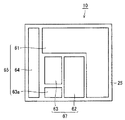
図1は、本実施の形態1に係る半導体集積回路装置(不揮発性半導体記憶装置)10を模式的に示した平面図である。この半導体集積回路装置10は、たとえば、MONOS(Metal Oxide Nitride Oxide Silicon)構造のフラッシュメモリが搭載された混載マイコンとして適用される。この半導体集積回路装置10は、基板上に周辺回路領域65と、メモリセル領域67とを備えている。
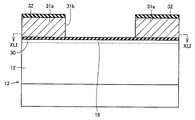
図6は、半導体集積回路装置10の製造工程の第1工程において、メモリセル領域67における断面図であり、図7は、第1工程における周辺回路領域65における断面図である。
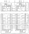
図30から図33および図39から図45を用いて、本実施の形態2に係る半導体集積回路装置10について説明する。図39は、本実施の形態2に係る半導体集積回路装置10のメモリセル領域67の平面図である。この図39に示されるように、半導体集積回路装置10は、メモリセル領域67が位置する半導体基板13の主表面上に選択的に形成された分離領域90と、この分離領域90によって規定された複数の分割メモリセル領域MCR1、MCR2と、各分割メモリセル領域MCR1、MCR2上に形成されたコントロールゲート42、メモリデート電極45同士を接続する接続領域PRとを備えている。
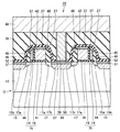
図46から図52を用いて、本実施の形態3に係る半導体集積回路装置10について説明する。なお、上記実施の形態1または実施の形態2に係る半導体集積回路装置10と同様の構成については、同一の符号を付してその説明を省略する。
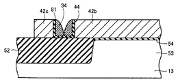
この図52に示されるように、導電膜パターン31aにパターニングを施して、コントロールゲート42を形成すると共に、他の周辺回路トランジスタのゲート電極もパターニングして形成する。
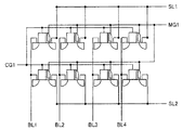
図53から図66を用いて、本実施の形態4に係る半導体集積回路装置10について、説明する。図53は、本実施の形態4に係る半導体集積回路装置10のたとえば、RAM領域62における平面図である。この図53に示されるように、RAM領域62が位置する半導体基板13の主表面上には、複数のSRAMのメモリセルM1〜M6が形成されている。
Claims (5)
- メモリセルトランジスタが形成されるメモリセル領域と、前記メモリセルトランジスタの動作制御を行なう周辺回路が形成される周辺回路領域とを有する半導体記憶装置の製造方法であって、
半導体基板の主表面上に選択的に分離領域を形成して、活性領域を規定する工程と、
前記活性領域上に第1絶縁膜を形成する工程と、
前記メモリセル領域において、第1導電膜を形成する工程と、
前記メモリセル領域において、前記第1導電膜にパターニングを施して、ソース領域として機能可能な第1不純物領域となる領域上に開口部を有する導電膜パターンを形成する工程と、
前記メモリセル領域の前記導電膜パターンをマスクとして、前記半導体基板の主表面に不純物を導入する工程と、
前記導電膜パターンを覆い、第1シリコン酸化膜とシリコン窒化膜と第2シリコン酸化膜から形成され、電荷を蓄積可能な第2絶縁膜を形成する工程と、
前記第2絶縁膜上に第2導電膜を形成する工程と、
前記メモリセル領域において、前記第2導電膜にエッチングを施して、前記導電膜パターンの開口部の側面に、2つの前記メモリセルトランジスタのサイドウォール形状のメモリゲート電極を同時に形成する工程と、
前記メモリセル領域において、前記導電膜パターンと、前記2つのメモリゲート電極をマスクとして、前記第1不純物領域を形成する工程と、
前記メモリセル領域において、前記導電膜パターンのうち、ドレイン領域として機能可能な第2不純物領域が位置する領域をエッチングし、パターニングすると同時に、前記周辺回路領域に形成されるトランジスタのゲート電極を形成する工程と、
前記半導体基板の主表面に不純物を導入して、前記メモリセルトランジスタの前記第2不純物領域と、前記周辺回路領域に形成されるトランジスタのソース領域、ドレイン領域とを形成する工程と、
を備え、
前記第1導電膜をパターニングして前記導電膜パターンを形成する工程は、前記メモリセルトランジスタの前記第1不純物領域となる領域上に、前記第1導電膜の残留部を残す工程を含み、
前記第2絶縁膜の形成工程は、前記残留部を覆うように前記第2絶縁膜を形成する工程を含み、
前記メモリゲート電極を形成する工程は、対向配置された前記メモリゲート電極を一体的に接続する接続部を、前記残留部の周囲に形成する工程を含み、
前記接続部上にコンタクト部を形成する工程をさらに備える、半導体記憶装置の製造方法。 - メモリセルトランジスタが形成されるメモリセル領域と、前記メモリセルトランジスタの動作制御を行なう周辺回路が形成される周辺回路領域とを有する半導体記憶装置の製造方法であって、
半導体基板の主表面上に選択的に分離領域を形成して、活性領域を規定する工程と、
前記活性領域上に第1絶縁膜を形成する工程と、
前記第1絶縁膜上に第1導電膜を形成する工程と、
前記メモリセル領域において、前記第1導電膜にパターニングを施して、ソース領域として機能可能な第1不純物領域となる領域上に開口部を形成すると共に、前記開口部の長手方向の両端部側に凹部を同時にパターニングして導電膜パターンを形成する工程と、
前記メモリセル領域において、前記導電膜パターンをマスクとして、前記半導体基板の主表面に不純物を導入する工程と、
前記導電膜パターンを覆い、第1シリコン酸化膜とシリコン窒化膜と第2シリコン酸化膜から形成され、電荷を蓄積可能な第2絶縁膜を形成する工程と、
前記第2絶縁膜上に第2導電膜を形成する工程と、
前記メモリセル領域において、前記第2導電膜にエッチングを施して、前記導電膜パターンの開口部の側面に、2つのメモリセルトランジスタのサイドウォール形状のメモリゲート電極を同時に形成する工程と、
前記メモリセル領域において、前記導電膜パターンと、前記2つのメモリゲート電極をマスクとして、第1不純物領域を形成する工程と、
前記メモリセル領域において、前記導電膜パターンのうち、ドレイン領域として機能可能な第2不純物領域が位置する領域をエッチングして、前記第1不純物領域の周囲を取り囲む環状のコントロールゲート電極を形成する工程と、
前記半導体基板の主表面に不純物を導入して前記第2不純物領域を形成する工程とを備え、
前記2つのメモリセルトランジスタの第1のメモリゲート電極と第2のメモリゲート電極はメモリセル領域の端部まで配線されてつながっていることを特徴とする、半導体記憶装置の製造方法。 - 前記第2絶縁膜上に第2導電膜を形成する工程は、前記凹部内に前記第2導電膜を充填することにより、前記メモリゲート電極に電圧を印加可能な電圧印加部が接続されるパッド部を形成する工程を含む、請求項2に記載の半導体記憶装置の製造方法。
- 前記コントロールゲート電極の上面にシリサイド膜を形成する工程をさらに備える、請求項2に記載の半導体記憶装置の製造方法。
- 前記第1不純物領域の周囲を取り囲む環状のコントロールゲート電極を形成すると同時に、前記周辺回路領域に形成されるトランジスタのゲート電極が形成されることを特徴とする、請求項2に記載の半導体記憶装置の製造方法。
Priority Applications (7)
| Application Number | Priority Date | Filing Date | Title |
|---|---|---|---|
| JP2006042255A JP5025140B2 (ja) | 2005-03-23 | 2006-02-20 | 半導体記憶装置の製造方法 |
| TW095109566A TWI382528B (zh) | 2005-03-23 | 2006-03-21 | 半導體記憶裝置及其製造方法 |
| US11/384,864 US7582550B2 (en) | 2005-03-23 | 2006-03-21 | Semiconductor memory device and manufacturing method thereof |
| KR1020060026177A KR101240720B1 (ko) | 2005-03-23 | 2006-03-22 | 반도체 기억 장치의 제조 방법 |
| CN2009101508015A CN101599461B (zh) | 2005-03-23 | 2006-03-23 | 半导体存储装置及其制造方法 |
| US12/504,146 US8174062B2 (en) | 2005-03-23 | 2009-07-16 | Semiconductor memory device and manufacturing method thereof |
| KR1020120090844A KR101210198B1 (ko) | 2005-03-23 | 2012-08-20 | 반도체 기억 장치 |
Applications Claiming Priority (3)
| Application Number | Priority Date | Filing Date | Title |
|---|---|---|---|
| JP2005083981 | 2005-03-23 | ||
| JP2005083981 | 2005-03-23 | ||
| JP2006042255A JP5025140B2 (ja) | 2005-03-23 | 2006-02-20 | 半導体記憶装置の製造方法 |
Related Child Applications (1)
| Application Number | Title | Priority Date | Filing Date |
|---|---|---|---|
| JP2012117181A Division JP2012191223A (ja) | 2005-03-23 | 2012-05-23 | 半導体記憶装置 |
Publications (3)
| Publication Number | Publication Date |
|---|---|
| JP2006303448A JP2006303448A (ja) | 2006-11-02 |
| JP2006303448A5 JP2006303448A5 (ja) | 2009-03-12 |
| JP5025140B2 true JP5025140B2 (ja) | 2012-09-12 |
Family
ID=37471318
Family Applications (1)
| Application Number | Title | Priority Date | Filing Date |
|---|---|---|---|
| JP2006042255A Expired - Fee Related JP5025140B2 (ja) | 2005-03-23 | 2006-02-20 | 半導体記憶装置の製造方法 |
Country Status (4)
| Country | Link |
|---|---|
| US (2) | US7582550B2 (ja) |
| JP (1) | JP5025140B2 (ja) |
| KR (2) | KR101240720B1 (ja) |
| TW (1) | TWI382528B (ja) |
Families Citing this family (15)
| Publication number | Priority date | Publication date | Assignee | Title |
|---|---|---|---|---|
| JP5190189B2 (ja) * | 2006-08-09 | 2013-04-24 | パナソニック株式会社 | 半導体装置及びその製造方法 |
| WO2008059768A1 (en) * | 2006-11-14 | 2008-05-22 | Nec Corporation | Semiconductor device |
| US8173532B2 (en) * | 2007-07-30 | 2012-05-08 | International Business Machines Corporation | Semiconductor transistors having reduced distances between gate electrode regions |
| JP2009124106A (ja) * | 2007-10-26 | 2009-06-04 | Renesas Technology Corp | 半導体装置およびその製造方法 |
| JP2009130136A (ja) | 2007-11-22 | 2009-06-11 | Renesas Technology Corp | 不揮発性半導体記憶装置およびその製造方法 |
| JP2010021465A (ja) * | 2008-07-14 | 2010-01-28 | Nec Electronics Corp | 不揮発性半導体記憶装置 |
| KR100936627B1 (ko) * | 2008-12-24 | 2010-01-13 | 주식회사 동부하이텍 | 플래시 메모리 소자 및 이의 제조 방법 |
| KR101510481B1 (ko) * | 2008-12-31 | 2015-04-10 | 주식회사 동부하이텍 | 플래시 메모리 소자 및 그 제조 방법 |
| WO2010082328A1 (ja) * | 2009-01-15 | 2010-07-22 | ルネサスエレクトロニクス株式会社 | 半導体装置およびその製造方法 |
| US8692310B2 (en) | 2009-02-09 | 2014-04-08 | Spansion Llc | Gate fringing effect based channel formation for semiconductor device |
| US8951864B2 (en) * | 2012-02-13 | 2015-02-10 | Taiwan Semiconductor Manufacturing Company, Ltd. | Split-gate device and method of fabricating the same |
| US8822289B2 (en) * | 2012-12-14 | 2014-09-02 | Spansion Llc | High voltage gate formation |
| JP5650303B2 (ja) * | 2013-10-29 | 2015-01-07 | ルネサスエレクトロニクス株式会社 | 半導体記憶装置の製造方法 |
| US9437603B2 (en) * | 2014-10-10 | 2016-09-06 | Taiwan Semiconductor Manufacturing Co., Ltd. | Wing-type projection between neighboring access transistors in memory devices |
| KR102618492B1 (ko) | 2018-05-18 | 2023-12-28 | 삼성전자주식회사 | 3차원 반도체 소자 |
Family Cites Families (20)
| Publication number | Priority date | Publication date | Assignee | Title |
|---|---|---|---|---|
| US5285093A (en) * | 1992-10-05 | 1994-02-08 | Motorola, Inc. | Semiconductor memory cell having a trench structure |
| KR970013338A (ko) * | 1995-08-21 | 1997-03-29 | 김광호 | 불휘발성 메모리 장치 및 그 제조 방법 |
| JP3621303B2 (ja) * | 1999-08-30 | 2005-02-16 | Necエレクトロニクス株式会社 | 半導体装置及びその製造方法 |
| KR100554833B1 (ko) * | 1999-10-11 | 2006-02-22 | 주식회사 하이닉스반도체 | 비휘발성 메모리 소자 및 그의 제조방법 |
| JP2002231829A (ja) * | 2001-01-22 | 2002-08-16 | Halo Lsi Design & Device Technol Inc | 不揮発性半導体メモリおよびその製造方法 |
| JP3496932B2 (ja) * | 2001-01-30 | 2004-02-16 | セイコーエプソン株式会社 | 不揮発性半導体記憶装置を含む半導体集積回路装置 |
| US7053459B2 (en) * | 2001-03-12 | 2006-05-30 | Renesas Technology Corp. | Semiconductor integrated circuit device and process for producing the same |
| JP4191975B2 (ja) * | 2001-11-01 | 2008-12-03 | イノテック株式会社 | トランジスタとそれを用いた半導体メモリ、およびトランジスタの製造方法 |
| US6894341B2 (en) * | 2001-12-25 | 2005-05-17 | Kabushiki Kaisha Toshiba | Semiconductor device and manufacturing method |
| JP4647175B2 (ja) | 2002-04-18 | 2011-03-09 | ルネサスエレクトロニクス株式会社 | 半導体集積回路装置 |
| JP2003330388A (ja) * | 2002-05-15 | 2003-11-19 | Semiconductor Energy Lab Co Ltd | 半導体装置及びその作製方法 |
| JP4134637B2 (ja) * | 2002-08-27 | 2008-08-20 | 株式会社日立製作所 | 半導体装置 |
| JP2004186452A (ja) * | 2002-12-04 | 2004-07-02 | Renesas Technology Corp | 不揮発性半導体記憶装置およびその製造方法 |
| KR100521371B1 (ko) | 2003-01-22 | 2005-10-12 | 삼성전자주식회사 | 소노스형 비휘발성 메모리 및 그 제조 방법 |
| JP2004241473A (ja) * | 2003-02-04 | 2004-08-26 | Renesas Technology Corp | 半導体記憶装置 |
| JP4718104B2 (ja) * | 2003-02-17 | 2011-07-06 | ルネサスエレクトロニクス株式会社 | 半導体装置 |
| JP2004335057A (ja) * | 2003-05-12 | 2004-11-25 | Sharp Corp | 誤作動防止装置付き半導体記憶装置とそれを用いた携帯電子機器 |
| US7214585B2 (en) * | 2003-05-16 | 2007-05-08 | Promos Technologies Inc. | Methods of fabricating integrated circuits with openings that allow electrical contact to conductive features having self-aligned edges |
| JP2004356562A (ja) | 2003-05-30 | 2004-12-16 | Renesas Technology Corp | 半導体装置の製造方法および半導体装置 |
| JP2005191489A (ja) * | 2003-12-26 | 2005-07-14 | Sharp Corp | 半導体記憶装置およびその製造方法 |
-
2006
- 2006-02-20 JP JP2006042255A patent/JP5025140B2/ja not_active Expired - Fee Related
- 2006-03-21 US US11/384,864 patent/US7582550B2/en active Active
- 2006-03-21 TW TW095109566A patent/TWI382528B/zh not_active IP Right Cessation
- 2006-03-22 KR KR1020060026177A patent/KR101240720B1/ko active IP Right Grant
-
2009
- 2009-07-16 US US12/504,146 patent/US8174062B2/en not_active Expired - Fee Related
-
2012
- 2012-08-20 KR KR1020120090844A patent/KR101210198B1/ko active IP Right Grant
Also Published As
| Publication number | Publication date |
|---|---|
| TW200717777A (en) | 2007-05-01 |
| US7582550B2 (en) | 2009-09-01 |
| US8174062B2 (en) | 2012-05-08 |
| TWI382528B (zh) | 2013-01-11 |
| KR101240720B1 (ko) | 2013-03-07 |
| JP2006303448A (ja) | 2006-11-02 |
| US20070221960A1 (en) | 2007-09-27 |
| KR20120097364A (ko) | 2012-09-03 |
| KR20060103153A (ko) | 2006-09-28 |
| US20090294827A1 (en) | 2009-12-03 |
| KR101210198B1 (ko) | 2012-12-07 |
Similar Documents
| Publication | Publication Date | Title |
|---|---|---|
| JP5025140B2 (ja) | 半導体記憶装置の製造方法 | |
| JP4928825B2 (ja) | 半導体装置の製造方法 | |
| US8084303B2 (en) | Semiconductor device and a method of manufacturing the same | |
| KR20110118752A (ko) | 반도체장치 및 그 제조방법 | |
| JP4291751B2 (ja) | 半導体記憶装置 | |
| KR100201451B1 (ko) | 불휘발성 기억장치 | |
| JP4405489B2 (ja) | 不揮発性半導体メモリ | |
| JP2012191223A (ja) | 半導体記憶装置 | |
| US8134201B2 (en) | Semiconductor memory device provided with stacked layer gate including charge accumulation layer and control gate, and manufacturing method thereof | |
| KR20070076444A (ko) | 반도체 기억 장치 및 그 제조 방법 | |
| CN101335305A (zh) | 非易失性存储器及其制造方法 | |
| JP6739327B2 (ja) | 半導体装置 | |
| JP2008187051A (ja) | 半導体記憶装置 | |
| JP2007208152A (ja) | 半導体装置およびその製造方法 | |
| JP2006344735A (ja) | 半導体装置 | |
| KR100202115B1 (ko) | 느타리 버섯 재배용 분말 종균 제조법 | |
| US20060171206A1 (en) | Non-volatile memory and fabricating method and operating method thereof | |
| JPWO2009096083A1 (ja) | 浮遊ゲート型不揮発性メモリ装置及びその製造方法 | |
| KR100201813B1 (ko) | 교환기시스템에서 이중화된 제어부의 절체회로 및 방법 | |
| JP4480541B2 (ja) | 不揮発性半導体記憶装置 | |
| JP2006080567A (ja) | 半導体集積回路装置およびその製造方法 | |
| JP2006324274A (ja) | 不揮発性半導体記憶装置およびその製造方法 | |
| JP2006228869A (ja) | 半導体記憶装置 | |
| JP2005101054A (ja) | 不揮発性半導体記憶装置およびその製造方法 |
Legal Events
| Date | Code | Title | Description |
|---|---|---|---|
| A521 | Request for written amendment filed |
Free format text: JAPANESE INTERMEDIATE CODE: A523 Effective date: 20090128 |
|
| A621 | Written request for application examination |
Free format text: JAPANESE INTERMEDIATE CODE: A621 Effective date: 20090128 |
|
| A711 | Notification of change in applicant |
Free format text: JAPANESE INTERMEDIATE CODE: A712 Effective date: 20100526 |
|
| A977 | Report on retrieval |
Free format text: JAPANESE INTERMEDIATE CODE: A971007 Effective date: 20111227 |
|
| A131 | Notification of reasons for refusal |
Free format text: JAPANESE INTERMEDIATE CODE: A131 Effective date: 20120417 |
|
| A521 | Request for written amendment filed |
Free format text: JAPANESE INTERMEDIATE CODE: A523 Effective date: 20120523 |
|
| TRDD | Decision of grant or rejection written | ||
| A01 | Written decision to grant a patent or to grant a registration (utility model) |
Free format text: JAPANESE INTERMEDIATE CODE: A01 Effective date: 20120612 |
|
| A01 | Written decision to grant a patent or to grant a registration (utility model) |
Free format text: JAPANESE INTERMEDIATE CODE: A01 |
|
| A61 | First payment of annual fees (during grant procedure) |
Free format text: JAPANESE INTERMEDIATE CODE: A61 Effective date: 20120619 |
|
| FPAY | Renewal fee payment (event date is renewal date of database) |
Free format text: PAYMENT UNTIL: 20150629 Year of fee payment: 3 |
|
| R150 | Certificate of patent or registration of utility model |
Ref document number: 5025140 Country of ref document: JP Free format text: JAPANESE INTERMEDIATE CODE: R150 Free format text: JAPANESE INTERMEDIATE CODE: R150 |
|
| S531 | Written request for registration of change of domicile |
Free format text: JAPANESE INTERMEDIATE CODE: R313531 |
|
| R350 | Written notification of registration of transfer |
Free format text: JAPANESE INTERMEDIATE CODE: R350 |
|
| LAPS | Cancellation because of no payment of annual fees |