JP6220597B2 - 半導体装置 - Google Patents
半導体装置 Download PDFInfo
- Publication number
- JP6220597B2 JP6220597B2 JP2013161530A JP2013161530A JP6220597B2 JP 6220597 B2 JP6220597 B2 JP 6220597B2 JP 2013161530 A JP2013161530 A JP 2013161530A JP 2013161530 A JP2013161530 A JP 2013161530A JP 6220597 B2 JP6220597 B2 JP 6220597B2
- Authority
- JP
- Japan
- Prior art keywords
- oxide semiconductor
- layer
- insulating layer
- film
- transistor
- Prior art date
- Legal status (The legal status is an assumption and is not a legal conclusion. Google has not performed a legal analysis and makes no representation as to the accuracy of the status listed.)
- Active
Links
Images


Classifications
-
- H—ELECTRICITY
- H10—SEMICONDUCTOR DEVICES; ELECTRIC SOLID-STATE DEVICES NOT OTHERWISE PROVIDED FOR
- H10D—INORGANIC ELECTRIC SEMICONDUCTOR DEVICES
- H10D30/00—Field-effect transistors [FET]
- H10D30/01—Manufacture or treatment
- H10D30/021—Manufacture or treatment of FETs having insulated gates [IGFET]
- H10D30/031—Manufacture or treatment of FETs having insulated gates [IGFET] of thin-film transistors [TFT]
-
- H—ELECTRICITY
- H10—SEMICONDUCTOR DEVICES; ELECTRIC SOLID-STATE DEVICES NOT OTHERWISE PROVIDED FOR
- H10B—ELECTRONIC MEMORY DEVICES
- H10B12/00—Dynamic random access memory [DRAM] devices
- H10B12/01—Manufacture or treatment
- H10B12/02—Manufacture or treatment for one transistor one-capacitor [1T-1C] memory cells
- H10B12/05—Making the transistor
-
- H—ELECTRICITY
- H10—SEMICONDUCTOR DEVICES; ELECTRIC SOLID-STATE DEVICES NOT OTHERWISE PROVIDED FOR
- H10B—ELECTRONIC MEMORY DEVICES
- H10B41/00—Electrically erasable-and-programmable ROM [EEPROM] devices comprising floating gates
- H10B41/70—Electrically erasable-and-programmable ROM [EEPROM] devices comprising floating gates the floating gate being an electrode shared by two or more components
-
- H—ELECTRICITY
- H10—SEMICONDUCTOR DEVICES; ELECTRIC SOLID-STATE DEVICES NOT OTHERWISE PROVIDED FOR
- H10D—INORGANIC ELECTRIC SEMICONDUCTOR DEVICES
- H10D30/00—Field-effect transistors [FET]
- H10D30/60—Insulated-gate field-effect transistors [IGFET]
- H10D30/67—Thin-film transistors [TFT]
- H10D30/6729—Thin-film transistors [TFT] characterised by the electrodes
- H10D30/6737—Thin-film transistors [TFT] characterised by the electrodes characterised by the electrode materials
- H10D30/6739—Conductor-insulator-semiconductor electrodes
-
- H—ELECTRICITY
- H10—SEMICONDUCTOR DEVICES; ELECTRIC SOLID-STATE DEVICES NOT OTHERWISE PROVIDED FOR
- H10D—INORGANIC ELECTRIC SEMICONDUCTOR DEVICES
- H10D30/00—Field-effect transistors [FET]
- H10D30/60—Insulated-gate field-effect transistors [IGFET]
- H10D30/751—Insulated-gate field-effect transistors [IGFET] having composition variations in the channel regions
-
- H—ELECTRICITY
- H10—SEMICONDUCTOR DEVICES; ELECTRIC SOLID-STATE DEVICES NOT OTHERWISE PROVIDED FOR
- H10D—INORGANIC ELECTRIC SEMICONDUCTOR DEVICES
- H10D62/00—Semiconductor bodies, or regions thereof, of devices having potential barriers
- H10D62/80—Semiconductor bodies, or regions thereof, of devices having potential barriers characterised by the materials
- H10D62/82—Heterojunctions
-
- H—ELECTRICITY
- H10—SEMICONDUCTOR DEVICES; ELECTRIC SOLID-STATE DEVICES NOT OTHERWISE PROVIDED FOR
- H10D—INORGANIC ELECTRIC SEMICONDUCTOR DEVICES
- H10D84/00—Integrated devices formed in or on semiconductor substrates that comprise only semiconducting layers, e.g. on Si wafers or on GaAs-on-Si wafers
- H10D84/90—Masterslice integrated circuits
- H10D84/903—Masterslice integrated circuits comprising field effect technology
- H10D84/907—CMOS gate arrays
-
- H—ELECTRICITY
- H10—SEMICONDUCTOR DEVICES; ELECTRIC SOLID-STATE DEVICES NOT OTHERWISE PROVIDED FOR
- H10D—INORGANIC ELECTRIC SEMICONDUCTOR DEVICES
- H10D86/00—Integrated devices formed in or on insulating or conducting substrates, e.g. formed in silicon-on-insulator [SOI] substrates or on stainless steel or glass substrates
- H10D86/40—Integrated devices formed in or on insulating or conducting substrates, e.g. formed in silicon-on-insulator [SOI] substrates or on stainless steel or glass substrates characterised by multiple TFTs
- H10D86/421—Integrated devices formed in or on insulating or conducting substrates, e.g. formed in silicon-on-insulator [SOI] substrates or on stainless steel or glass substrates characterised by multiple TFTs having a particular composition, shape or crystalline structure of the active layer
- H10D86/423—Integrated devices formed in or on insulating or conducting substrates, e.g. formed in silicon-on-insulator [SOI] substrates or on stainless steel or glass substrates characterised by multiple TFTs having a particular composition, shape or crystalline structure of the active layer comprising semiconductor materials not belonging to the Group IV, e.g. InGaZnO
-
- H—ELECTRICITY
- H10—SEMICONDUCTOR DEVICES; ELECTRIC SOLID-STATE DEVICES NOT OTHERWISE PROVIDED FOR
- H10D—INORGANIC ELECTRIC SEMICONDUCTOR DEVICES
- H10D86/00—Integrated devices formed in or on insulating or conducting substrates, e.g. formed in silicon-on-insulator [SOI] substrates or on stainless steel or glass substrates
- H10D86/40—Integrated devices formed in or on insulating or conducting substrates, e.g. formed in silicon-on-insulator [SOI] substrates or on stainless steel or glass substrates characterised by multiple TFTs
- H10D86/60—Integrated devices formed in or on insulating or conducting substrates, e.g. formed in silicon-on-insulator [SOI] substrates or on stainless steel or glass substrates characterised by multiple TFTs wherein the TFTs are in active matrices
-
- H—ELECTRICITY
- H10—SEMICONDUCTOR DEVICES; ELECTRIC SOLID-STATE DEVICES NOT OTHERWISE PROVIDED FOR
- H10P—GENERIC PROCESSES OR APPARATUS FOR THE MANUFACTURE OR TREATMENT OF DEVICES COVERED BY CLASS H10
- H10P95/00—Generic processes or apparatus for manufacture or treatments not covered by the other groups of this subclass
- H10P95/06—Planarisation of inorganic insulating materials
-
- H—ELECTRICITY
- H10—SEMICONDUCTOR DEVICES; ELECTRIC SOLID-STATE DEVICES NOT OTHERWISE PROVIDED FOR
- H10P—GENERIC PROCESSES OR APPARATUS FOR THE MANUFACTURE OR TREATMENT OF DEVICES COVERED BY CLASS H10
- H10P95/00—Generic processes or apparatus for manufacture or treatments not covered by the other groups of this subclass
- H10P95/90—Thermal treatments, e.g. annealing or sintering
Landscapes
- Engineering & Computer Science (AREA)
- Manufacturing & Machinery (AREA)
- Thin Film Transistor (AREA)
- Semiconductor Memories (AREA)
- Metal-Oxide And Bipolar Metal-Oxide Semiconductor Integrated Circuits (AREA)
- Electroluminescent Light Sources (AREA)
- Non-Volatile Memory (AREA)
- Physical Vapour Deposition (AREA)
Description
本実施の形態では、本発明の一態様の半導体装置について、図面を用いて詳細に説明する。図1に本発明の一態様の半導体装置を示す。
実施の形態1に示す半導体装置の一例として、論理回路であるNOR型回路の回路図の一例を図6(A)に示す。図6(B)はNAND型回路の回路図である。
本実施の形態では、実施の形態1に示す半導体装置を使用し、電力が供給されない状況でも記憶内容の保持が可能で、かつ、書き込み回数にも制限が無い半導体装置(記憶装置)の一例を、図面を用いて説明する。
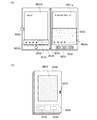
本実施の形態では、先の実施の形態で示した半導体装置を携帯電話、スマートフォン、電子書籍などの電子機器に応用した場合の例を図8乃至図11を用いて説明する。
102 素子分離絶縁層
104 絶縁層
108 ゲート絶縁層
110 ゲート電極層
112 配線層
114 配線層
115 配線層
115a 配線層
115b 配線層
115c 配線層
116 配線層
117 配線層
120 絶縁層
135 絶縁層
140 絶縁層
142a ソース電極層
142b ドレイン電極層
144 酸化物半導体積層
144a 酸化物半導体層
144b 酸化物半導体層
144c 酸化物半導体層
147 ゲート絶縁層
147a ゲート絶縁層
147b ゲート絶縁層
148 ゲート電極層
149 ゲート電極層
150 絶縁層
155 絶縁層
160 トランジスタ
162 トランジスタ
163 トランジスタ
164 トランジスタ
172 トランジスタ
173 トランジスタ
174 トランジスタ
250 メモリセル
251 メモリセルアレイ
251a メモリセルアレイ
251b メモリセルアレイ
253 周辺回路
254 容量素子
260 トランジスタ
262 トランジスタ
264 容量素子
801 トランジスタ
802 トランジスタ
803 トランジスタ
804 トランジスタ
811 トランジスタ
812 トランジスタ
813 トランジスタ
814 トランジスタ
901 RF回路
902 アナログベースバンド回路
903 デジタルベースバンド回路
904 バッテリー
905 電源回路
906 アプリケーションプロセッサ
907 CPU
908 DSP
910 フラッシュメモリ
911 ディスプレイコントローラ
912 メモリ回路
913 ディスプレイ
914 表示部
915 ソースドライバ
916 ゲートドライバ
917 音声回路
918 キーボード
919 タッチセンサ
950 メモリ回路
951 メモリコントローラ
952 メモリ
953 メモリ
954 スイッチ
955 スイッチ
956 ディスプレイコントローラ
957 ディスプレイ
1001 バッテリー
1002 電源回路
1003 マイクロプロセッサ
1004 フラッシュメモリ
1005 音声回路
1006 キーボード
1007 メモリ回路
1008 タッチパネル
1009 ディスプレイ
1010 ディスプレイコントローラ
9033 留め具
9034 スイッチ
9035 電源スイッチ
9036 スイッチ
9038 操作スイッチ
9630 筐体
9631a 表示部
9631b 表示部
9632a 領域
9632b 領域
9633 太陽電池
9634 充放電制御回路
9635 バッテリー
9636 DCDCコンバータ
9638 操作キー
9639 ボタン
Claims (3)
- 半導体基板上方の第1の酸化物絶縁層と、
前記第1の酸化物絶縁層上方の金属酸化物層と、
前記金属酸化物層上方の第2の酸化物絶縁層と、
前記第2の酸化物絶縁層を介して前記金属酸化物層と重なるゲート電極層と、を有し、
前記金属酸化物層は、第1乃至第3の金属酸化物層が順に積層された構造を有し、
前記第1乃至前記第3の金属酸化物層は少なくともインジウムを含み、
前記第2の金属酸化物層は、前記第1及び前記第3の金属酸化物層よりもインジウムの含有率が多く、
前記第2の金属酸化物層は結晶構造を有することを特徴とする半導体装置。 - 半導体基板上方の第1の窒化物絶縁層と、
前記第1の窒化物絶縁層上方の第1の酸化物絶縁層と、
前記第1の酸化物絶縁層上方の金属酸化物層と、
前記金属酸化物層上方の第2の酸化物絶縁層と、
前記第2の酸化物絶縁層上方の第2の窒化物絶縁層と、
前記第2の酸化物絶縁層及び前記第2の窒化物絶縁層を介して前記金属酸化物層と重なるゲート電極層と、を有し、
前記金属酸化物層は、第1乃至第3の金属酸化物層が順に積層された構造を有し、
前記第1乃至前記第3の金属酸化物層は少なくともインジウムを含み、
前記第2の金属酸化物層は、前記第1及び前記第3の金属酸化物層よりもインジウムの含有率が多く、
前記第2の金属酸化物層は結晶構造を有することを特徴とする半導体装置。 - 請求項1または請求項2において、
前記金属酸化物層は、局在準位による吸収係数が3×10⁻³/cm以下であること特徴とする半導体装置。
Priority Applications (1)
| Application Number | Priority Date | Filing Date | Title |
|---|---|---|---|
| JP2013161530A JP6220597B2 (ja) | 2012-08-10 | 2013-08-02 | 半導体装置 |
Applications Claiming Priority (3)
| Application Number | Priority Date | Filing Date | Title |
|---|---|---|---|
| JP2012178641 | 2012-08-10 | ||
| JP2012178641 | 2012-08-10 | ||
| JP2013161530A JP6220597B2 (ja) | 2012-08-10 | 2013-08-02 | 半導体装置 |
Related Child Applications (1)
| Application Number | Title | Priority Date | Filing Date |
|---|---|---|---|
| JP2017192493A Division JP6463434B2 (ja) | 2012-08-10 | 2017-10-02 | 半導体装置 |
Publications (3)
| Publication Number | Publication Date |
|---|---|
| JP2014057052A JP2014057052A (ja) | 2014-03-27 |
| JP2014057052A5 JP2014057052A5 (ja) | 2016-09-15 |
| JP6220597B2 true JP6220597B2 (ja) | 2017-10-25 |
Family
ID=50065527
Family Applications (7)
| Application Number | Title | Priority Date | Filing Date |
|---|---|---|---|
| JP2013161530A Active JP6220597B2 (ja) | 2012-08-10 | 2013-08-02 | 半導体装置 |
| JP2017192493A Expired - Fee Related JP6463434B2 (ja) | 2012-08-10 | 2017-10-02 | 半導体装置 |
| JP2018246562A Expired - Fee Related JP6622379B2 (ja) | 2012-08-10 | 2018-12-28 | 半導体装置 |
| JP2019210235A Active JP6840214B2 (ja) | 2012-08-10 | 2019-11-21 | 半導体装置 |
| JP2021022508A Active JP7199458B2 (ja) | 2012-08-10 | 2021-02-16 | 半導体装置 |
| JP2022203009A Active JP7403619B2 (ja) | 2012-08-10 | 2022-12-20 | 半導体装置 |
| JP2023209600A Active JP7585443B2 (ja) | 2012-08-10 | 2023-12-12 | 半導体装置 |
Family Applications After (6)
| Application Number | Title | Priority Date | Filing Date |
|---|---|---|---|
| JP2017192493A Expired - Fee Related JP6463434B2 (ja) | 2012-08-10 | 2017-10-02 | 半導体装置 |
| JP2018246562A Expired - Fee Related JP6622379B2 (ja) | 2012-08-10 | 2018-12-28 | 半導体装置 |
| JP2019210235A Active JP6840214B2 (ja) | 2012-08-10 | 2019-11-21 | 半導体装置 |
| JP2021022508A Active JP7199458B2 (ja) | 2012-08-10 | 2021-02-16 | 半導体装置 |
| JP2022203009A Active JP7403619B2 (ja) | 2012-08-10 | 2022-12-20 | 半導体装置 |
| JP2023209600A Active JP7585443B2 (ja) | 2012-08-10 | 2023-12-12 | 半導体装置 |
Country Status (2)
| Country | Link |
|---|---|
| US (2) | US9184245B2 (ja) |
| JP (7) | JP6220597B2 (ja) |
Families Citing this family (53)
| Publication number | Priority date | Publication date | Assignee | Title |
|---|---|---|---|---|
| KR102304125B1 (ko) | 2011-09-29 | 2021-09-17 | 가부시키가이샤 한도오따이 에네루기 켄큐쇼 | 반도체 장치 |
| CN103843146B (zh) * | 2011-09-29 | 2016-03-16 | 株式会社半导体能源研究所 | 半导体器件 |
| SG11201504615UA (en) | 2011-10-14 | 2015-07-30 | Semiconductor Energy Lab | Semiconductor device |
| KR20130040706A (ko) | 2011-10-14 | 2013-04-24 | 가부시키가이샤 한도오따이 에네루기 켄큐쇼 | 반도체 장치 및 반도체 장치의 제작 방법 |
| JP2014027263A (ja) | 2012-06-15 | 2014-02-06 | Semiconductor Energy Lab Co Ltd | 半導体装置およびその作製方法 |
| JP6224931B2 (ja) | 2012-07-27 | 2017-11-01 | 株式会社半導体エネルギー研究所 | 半導体装置 |
| JP6134598B2 (ja) | 2012-08-02 | 2017-05-24 | 株式会社半導体エネルギー研究所 | 半導体装置 |
| US9929276B2 (en) | 2012-08-10 | 2018-03-27 | Semiconductor Energy Laboratory Co., Ltd. | Semiconductor device and method for manufacturing the same |
| KR102171650B1 (ko) | 2012-08-10 | 2020-10-29 | 가부시키가이샤 한도오따이 에네루기 켄큐쇼 | 반도체 장치 및 그 제작 방법 |
| WO2014024808A1 (en) | 2012-08-10 | 2014-02-13 | Semiconductor Energy Laboratory Co., Ltd. | Semiconductor device and manufacturing method thereof |
| US9245958B2 (en) | 2012-08-10 | 2016-01-26 | Semiconductor Energy Laboratory Co., Ltd. | Semiconductor device and method for manufacturing the same |
| CN104584229B (zh) | 2012-08-10 | 2018-05-15 | 株式会社半导体能源研究所 | 半导体装置及其制造方法 |
| WO2014046222A1 (en) | 2012-09-24 | 2014-03-27 | Semiconductor Energy Laboratory Co., Ltd. | Display device |
| TWI671910B (zh) | 2012-09-24 | 2019-09-11 | 日商半導體能源研究所股份有限公司 | 半導體裝置 |
| WO2014061762A1 (en) | 2012-10-17 | 2014-04-24 | Semiconductor Energy Laboratory Co., Ltd. | Semiconductor device and method for manufacturing the same |
| KR102220279B1 (ko) | 2012-10-19 | 2021-02-24 | 가부시키가이샤 한도오따이 에네루기 켄큐쇼 | 산화물 반도체막을 포함하는 다층막 및 반도체 장치의 제작 방법 |
| TWI582993B (zh) | 2012-11-30 | 2017-05-11 | 半導體能源研究所股份有限公司 | 半導體裝置 |
| WO2014103901A1 (en) | 2012-12-25 | 2014-07-03 | Semiconductor Energy Laboratory Co., Ltd. | Semiconductor device and method for manufacturing the same |
| KR102495290B1 (ko) | 2012-12-28 | 2023-02-06 | 가부시키가이샤 한도오따이 에네루기 켄큐쇼 | 반도체 장치 |
| US20150008428A1 (en) | 2013-07-08 | 2015-01-08 | Semiconductor Energy Laboratory Co., Ltd. | Semiconductor device and method for manufacturing semiconductor device |
| US9455349B2 (en) | 2013-10-22 | 2016-09-27 | Semiconductor Energy Laboratory Co., Ltd. | Oxide semiconductor thin film transistor with reduced impurity diffusion |
| KR102220450B1 (ko) * | 2013-12-02 | 2021-02-25 | 가부시키가이샤 한도오따이 에네루기 켄큐쇼 | 표시 장치 |
| JP6180908B2 (ja) * | 2013-12-06 | 2017-08-16 | 富士フイルム株式会社 | 金属酸化物半導体膜、薄膜トランジスタ、表示装置、イメージセンサ及びx線センサ |
| TWI721409B (zh) | 2013-12-19 | 2021-03-11 | 日商半導體能源研究所股份有限公司 | 半導體裝置 |
| US9917110B2 (en) * | 2014-03-14 | 2018-03-13 | Semiconductor Energy Laboratory Co., Ltd. | Semiconductor device |
| JP6486712B2 (ja) * | 2014-04-30 | 2019-03-20 | 株式会社半導体エネルギー研究所 | 酸化物半導体膜 |
| TWI663726B (zh) | 2014-05-30 | 2019-06-21 | Semiconductor Energy Laboratory Co., Ltd. | 半導體裝置、模組及電子裝置 |
| JP6705663B2 (ja) * | 2015-03-06 | 2020-06-03 | 株式会社半導体エネルギー研究所 | 半導体装置およびその作製方法 |
| US10147823B2 (en) * | 2015-03-19 | 2018-12-04 | Semiconductor Energy Laboratory Co., Ltd. | Semiconductor device |
| US9842938B2 (en) | 2015-03-24 | 2017-12-12 | Semiconductor Energy Laboratory Co., Ltd. | Semiconductor device and display device including semiconductor device |
| KR20160114511A (ko) | 2015-03-24 | 2016-10-05 | 가부시키가이샤 한도오따이 에네루기 켄큐쇼 | 반도체 장치의 제작 방법 |
| US10096715B2 (en) * | 2015-03-26 | 2018-10-09 | Semiconductor Energy Laboratory Co., Ltd. | Semiconductor device, method for manufacturing the same, and electronic device |
| US9806200B2 (en) | 2015-03-27 | 2017-10-31 | Semiconductor Energy Laboratory Co., Ltd. | Semiconductor device |
| US20170063112A1 (en) * | 2015-08-31 | 2017-03-02 | Semiconductor Energy Laboratory Co., Ltd. | Power storage device with monitoring ic |
| US10714633B2 (en) | 2015-12-15 | 2020-07-14 | Semiconductor Energy Laboratory Co., Ltd. | Semiconductor device and display device |
| US9917207B2 (en) * | 2015-12-25 | 2018-03-13 | Semiconductor Energy Laboratory Co., Ltd. | Semiconductor device and method for manufacturing the same |
| JP6853663B2 (ja) * | 2015-12-28 | 2021-03-31 | 株式会社半導体エネルギー研究所 | 半導体装置 |
| JP2017143135A (ja) * | 2016-02-09 | 2017-08-17 | 株式会社ジャパンディスプレイ | 薄膜トランジスタ |
| CN115954389A (zh) | 2016-03-04 | 2023-04-11 | 株式会社半导体能源研究所 | 半导体装置以及包括该半导体装置的显示装置 |
| KR20180123028A (ko) | 2016-03-11 | 2018-11-14 | 가부시키가이샤 한도오따이 에네루기 켄큐쇼 | 반도체 장비, 상기 반도체 장치의 제작 방법, 및 상기 반도체 장치를 포함하는 표시 장치 |
| CN109075206B (zh) | 2016-04-13 | 2022-08-16 | 株式会社半导体能源研究所 | 半导体装置及包括该半导体装置的显示装置 |
| WO2017199128A1 (en) * | 2016-05-20 | 2017-11-23 | Semiconductor Energy Laboratory Co., Ltd. | Semiconductor device or display device including the same |
| DE112017004841B4 (de) * | 2016-09-27 | 2025-04-17 | Sharp Kabushiki Kaisha | Halbleitervorrichtung und Verfahren zu deren Herstellung |
| US10756118B2 (en) * | 2016-11-30 | 2020-08-25 | Semiconductor Energy Laboratory Co., Ltd. | Display device, display module, and electronic device |
| JP7200121B2 (ja) | 2017-11-09 | 2023-01-06 | 株式会社半導体エネルギー研究所 | 半導体装置 |
| JP2019114751A (ja) * | 2017-12-26 | 2019-07-11 | シャープ株式会社 | 薄膜トランジスタ基板及びそれを備えた液晶表示装置並びに薄膜トランジスタ基板の製造方法 |
| US11355082B2 (en) | 2018-02-01 | 2022-06-07 | Semiconductor Energy Laboratory Co., Ltd. | Display device and electronic device |
| JP2021150525A (ja) | 2020-03-19 | 2021-09-27 | キオクシア株式会社 | 半導体記憶装置及び半導体記憶装置の製造方法 |
| KR102753300B1 (ko) * | 2020-06-27 | 2025-01-09 | 어플라이드 머티어리얼스, 인코포레이티드 | 박막 전기-광학 도파관 변조기 디바이스 |
| US11721767B2 (en) | 2020-06-29 | 2023-08-08 | Taiwan Semiconductor Manufacturing Company Limited | Oxide semiconductor transistor structure in 3-D device and methods of forming the same |
| KR20230063666A (ko) | 2021-11-02 | 2023-05-09 | 삼성전자주식회사 | 반도체 소자 |
| KR20230133149A (ko) * | 2022-03-10 | 2023-09-19 | 삼성전자주식회사 | 반도체 메모리 소자 |
| KR20230139545A (ko) * | 2022-03-28 | 2023-10-05 | 삼성전자주식회사 | 반도체 소자 및 이를 포함하는 반도체 메모리 셀 |
Family Cites Families (165)
| Publication number | Priority date | Publication date | Assignee | Title |
|---|---|---|---|---|
| JPS60198861A (ja) | 1984-03-23 | 1985-10-08 | Fujitsu Ltd | 薄膜トランジスタ |
| JPH0244256B2 (ja) | 1987-01-28 | 1990-10-03 | Kagaku Gijutsucho Mukizaishitsu Kenkyushocho | Ingazn2o5deshimesarerurotsuhoshokeinosojokozoojusurukagobutsuoyobisonoseizoho |
| JPH0244258B2 (ja) | 1987-02-24 | 1990-10-03 | Kagaku Gijutsucho Mukizaishitsu Kenkyushocho | Ingazn3o6deshimesarerurotsuhoshokeinosojokozoojusurukagobutsuoyobisonoseizoho |
| JPS63210023A (ja) | 1987-02-24 | 1988-08-31 | Natl Inst For Res In Inorg Mater | InGaZn↓4O↓7で示される六方晶系の層状構造を有する化合物およびその製造法 |
| JPH0244260B2 (ja) | 1987-02-24 | 1990-10-03 | Kagaku Gijutsucho Mukizaishitsu Kenkyushocho | Ingazn5o8deshimesarerurotsuhoshokeinosojokozoojusurukagobutsuoyobisonoseizoho |
| JPH0244262B2 (ja) | 1987-02-27 | 1990-10-03 | Kagaku Gijutsucho Mukizaishitsu Kenkyushocho | Ingazn6o9deshimesarerurotsuhoshokeinosojokozoojusurukagobutsuoyobisonoseizoho |
| JPH0244263B2 (ja) | 1987-04-22 | 1990-10-03 | Kagaku Gijutsucho Mukizaishitsu Kenkyushocho | Ingazn7o10deshimesarerurotsuhoshokeinosojokozoojusurukagobutsuoyobisonoseizoho |
| JPH05251705A (ja) | 1992-03-04 | 1993-09-28 | Fuji Xerox Co Ltd | 薄膜トランジスタ |
| JP3479375B2 (ja) | 1995-03-27 | 2003-12-15 | 科学技術振興事業団 | 亜酸化銅等の金属酸化物半導体による薄膜トランジスタとpn接合を形成した金属酸化物半導体装置およびそれらの製造方法 |
| DE69635107D1 (de) | 1995-08-03 | 2005-09-29 | Koninkl Philips Electronics Nv | Halbleiteranordnung mit einem transparenten schaltungselement |
| JP3625598B2 (ja) | 1995-12-30 | 2005-03-02 | 三星電子株式会社 | 液晶表示装置の製造方法 |
| JP4170454B2 (ja) | 1998-07-24 | 2008-10-22 | Hoya株式会社 | 透明導電性酸化物薄膜を有する物品及びその製造方法 |
| JP2000150861A (ja) | 1998-11-16 | 2000-05-30 | Tdk Corp | 酸化物薄膜 |
| JP3276930B2 (ja) | 1998-11-17 | 2002-04-22 | 科学技術振興事業団 | トランジスタ及び半導体装置 |
| TW460731B (en) | 1999-09-03 | 2001-10-21 | Ind Tech Res Inst | Electrode structure and production method of wide viewing angle LCD |
| JP4089858B2 (ja) | 2000-09-01 | 2008-05-28 | 国立大学法人東北大学 | 半導体デバイス |
| KR20020038482A (ko) | 2000-11-15 | 2002-05-23 | 모리시타 요이찌 | 박막 트랜지스터 어레이, 그 제조방법 및 그것을 이용한표시패널 |
| JP3997731B2 (ja) | 2001-03-19 | 2007-10-24 | 富士ゼロックス株式会社 | 基材上に結晶性半導体薄膜を形成する方法 |
| JP2002289859A (ja) | 2001-03-23 | 2002-10-04 | Minolta Co Ltd | 薄膜トランジスタ |
| JP3925839B2 (ja) | 2001-09-10 | 2007-06-06 | シャープ株式会社 | 半導体記憶装置およびその試験方法 |
| JP4090716B2 (ja) | 2001-09-10 | 2008-05-28 | 雅司 川崎 | 薄膜トランジスタおよびマトリクス表示装置 |
| JP4164562B2 (ja) | 2002-09-11 | 2008-10-15 | 独立行政法人科学技術振興機構 | ホモロガス薄膜を活性層として用いる透明薄膜電界効果型トランジスタ |
| WO2003040441A1 (fr) | 2001-11-05 | 2003-05-15 | Japan Science And Technology Agency | Film mince monocristallin homologue a super-reseau naturel, procede de preparation et dispositif dans lequel est utilise ledit film mince monocristallin |
| JP4083486B2 (ja) | 2002-02-21 | 2008-04-30 | 独立行政法人科学技術振興機構 | LnCuO(S,Se,Te)単結晶薄膜の製造方法 |
| US7049190B2 (en) | 2002-03-15 | 2006-05-23 | Sanyo Electric Co., Ltd. | Method for forming ZnO film, method for forming ZnO semiconductor layer, method for fabricating semiconductor device, and semiconductor device |
| JP3933591B2 (ja) | 2002-03-26 | 2007-06-20 | 淳二 城戸 | 有機エレクトロルミネッセント素子 |
| US7339187B2 (en) | 2002-05-21 | 2008-03-04 | State Of Oregon Acting By And Through The Oregon State Board Of Higher Education On Behalf Of Oregon State University | Transistor structures |
| JP2004022625A (ja) | 2002-06-13 | 2004-01-22 | Murata Mfg Co Ltd | 半導体デバイス及び該半導体デバイスの製造方法 |
| US7105868B2 (en) | 2002-06-24 | 2006-09-12 | Cermet, Inc. | High-electron mobility transistor with zinc oxide |
| US7067843B2 (en) | 2002-10-11 | 2006-06-27 | E. I. Du Pont De Nemours And Company | Transparent oxide semiconductor thin film transistors |
| JP4166105B2 (ja) | 2003-03-06 | 2008-10-15 | シャープ株式会社 | 半導体装置およびその製造方法 |
| JP2004273732A (ja) | 2003-03-07 | 2004-09-30 | Sharp Corp | アクティブマトリクス基板およびその製造方法 |
| JP4108633B2 (ja) | 2003-06-20 | 2008-06-25 | シャープ株式会社 | 薄膜トランジスタおよびその製造方法ならびに電子デバイス |
| US7262463B2 (en) | 2003-07-25 | 2007-08-28 | Hewlett-Packard Development Company, L.P. | Transistor including a deposited channel region having a doped portion |
| US7282782B2 (en) | 2004-03-12 | 2007-10-16 | Hewlett-Packard Development Company, L.P. | Combined binary oxide semiconductor device |
| US7297977B2 (en) | 2004-03-12 | 2007-11-20 | Hewlett-Packard Development Company, L.P. | Semiconductor device |
| US7145174B2 (en) | 2004-03-12 | 2006-12-05 | Hewlett-Packard Development Company, Lp. | Semiconductor device |
| EP1737044B1 (en) | 2004-03-12 | 2014-12-10 | Japan Science and Technology Agency | Amorphous oxide and thin film transistor |
| US7211825B2 (en) | 2004-06-14 | 2007-05-01 | Yi-Chi Shih | Indium oxide-based thin film transistors and circuits |
| JP2006100760A (ja) | 2004-09-02 | 2006-04-13 | Casio Comput Co Ltd | 薄膜トランジスタおよびその製造方法 |
| US7285501B2 (en) | 2004-09-17 | 2007-10-23 | Hewlett-Packard Development Company, L.P. | Method of forming a solution processed device |
| US7298084B2 (en) | 2004-11-02 | 2007-11-20 | 3M Innovative Properties Company | Methods and displays utilizing integrated zinc oxide row and column drivers in conjunction with organic light emitting diodes |
| CN102945857B (zh) | 2004-11-10 | 2015-06-03 | 佳能株式会社 | 无定形氧化物和场效应晶体管 |
| WO2006051995A1 (en) | 2004-11-10 | 2006-05-18 | Canon Kabushiki Kaisha | Field effect transistor employing an amorphous oxide |
| US7453065B2 (en) | 2004-11-10 | 2008-11-18 | Canon Kabushiki Kaisha | Sensor and image pickup device |
| JP5138163B2 (ja) | 2004-11-10 | 2013-02-06 | キヤノン株式会社 | 電界効果型トランジスタ |
| JP5126729B2 (ja) | 2004-11-10 | 2013-01-23 | キヤノン株式会社 | 画像表示装置 |
| RU2358354C2 (ru) | 2004-11-10 | 2009-06-10 | Кэнон Кабусики Кайся | Светоизлучающее устройство |
| US7791072B2 (en) | 2004-11-10 | 2010-09-07 | Canon Kabushiki Kaisha | Display |
| US7829444B2 (en) | 2004-11-10 | 2010-11-09 | Canon Kabushiki Kaisha | Field effect transistor manufacturing method |
| US7863611B2 (en) | 2004-11-10 | 2011-01-04 | Canon Kabushiki Kaisha | Integrated circuits utilizing amorphous oxides |
| US7579224B2 (en) | 2005-01-21 | 2009-08-25 | Semiconductor Energy Laboratory Co., Ltd. | Method for manufacturing a thin film semiconductor device |
| TWI505473B (zh) | 2005-01-28 | 2015-10-21 | 半導體能源研究所股份有限公司 | 半導體裝置,電子裝置,和半導體裝置的製造方法 |
| TWI569441B (zh) | 2005-01-28 | 2017-02-01 | 半導體能源研究所股份有限公司 | 半導體裝置,電子裝置,和半導體裝置的製造方法 |
| US7858451B2 (en) | 2005-02-03 | 2010-12-28 | Semiconductor Energy Laboratory Co., Ltd. | Electronic device, semiconductor device and manufacturing method thereof |
| US7948171B2 (en) | 2005-02-18 | 2011-05-24 | Semiconductor Energy Laboratory Co., Ltd. | Light emitting device |
| US20060197092A1 (en) | 2005-03-03 | 2006-09-07 | Randy Hoffman | System and method for forming conductive material on a substrate |
| US8681077B2 (en) | 2005-03-18 | 2014-03-25 | Semiconductor Energy Laboratory Co., Ltd. | Semiconductor device, and display device, driving method and electronic apparatus thereof |
| US7544967B2 (en) | 2005-03-28 | 2009-06-09 | Massachusetts Institute Of Technology | Low voltage flexible organic/transparent transistor for selective gas sensing, photodetecting and CMOS device applications |
| US7645478B2 (en) | 2005-03-31 | 2010-01-12 | 3M Innovative Properties Company | Methods of making displays |
| US8300031B2 (en) | 2005-04-20 | 2012-10-30 | Semiconductor Energy Laboratory Co., Ltd. | Semiconductor device comprising transistor having gate and drain connected through a current-voltage conversion element |
| JP2006344849A (ja) | 2005-06-10 | 2006-12-21 | Casio Comput Co Ltd | 薄膜トランジスタ |
| US7691666B2 (en) | 2005-06-16 | 2010-04-06 | Eastman Kodak Company | Methods of making thin film transistors comprising zinc-oxide-based semiconductor materials and transistors made thereby |
| US7402506B2 (en) | 2005-06-16 | 2008-07-22 | Eastman Kodak Company | Methods of making thin film transistors comprising zinc-oxide-based semiconductor materials and transistors made thereby |
| US7507618B2 (en) | 2005-06-27 | 2009-03-24 | 3M Innovative Properties Company | Method for making electronic devices using metal oxide nanoparticles |
| KR100711890B1 (ko) | 2005-07-28 | 2007-04-25 | 삼성에스디아이 주식회사 | 유기 발광표시장치 및 그의 제조방법 |
| JP2007059128A (ja) | 2005-08-23 | 2007-03-08 | Canon Inc | 有機el表示装置およびその製造方法 |
| JP2007073705A (ja) | 2005-09-06 | 2007-03-22 | Canon Inc | 酸化物半導体チャネル薄膜トランジスタおよびその製造方法 |
| JP4280736B2 (ja) | 2005-09-06 | 2009-06-17 | キヤノン株式会社 | 半導体素子 |
| JP4850457B2 (ja) | 2005-09-06 | 2012-01-11 | キヤノン株式会社 | 薄膜トランジスタ及び薄膜ダイオード |
| JP5116225B2 (ja) | 2005-09-06 | 2013-01-09 | キヤノン株式会社 | 酸化物半導体デバイスの製造方法 |
| JP5078246B2 (ja) | 2005-09-29 | 2012-11-21 | 株式会社半導体エネルギー研究所 | 半導体装置、及び半導体装置の作製方法 |
| EP1995787A3 (en) | 2005-09-29 | 2012-01-18 | Semiconductor Energy Laboratory Co, Ltd. | Semiconductor device having oxide semiconductor layer and manufacturing method therof |
| JP5037808B2 (ja) | 2005-10-20 | 2012-10-03 | キヤノン株式会社 | アモルファス酸化物を用いた電界効果型トランジスタ、及び該トランジスタを用いた表示装置 |
| KR101050767B1 (ko) | 2005-11-15 | 2011-07-20 | 가부시키가이샤 한도오따이 에네루기 켄큐쇼 | 반도체장치 제조방법 |
| TWI292281B (en) | 2005-12-29 | 2008-01-01 | Ind Tech Res Inst | Pixel structure of active organic light emitting diode and method of fabricating the same |
| US7867636B2 (en) | 2006-01-11 | 2011-01-11 | Murata Manufacturing Co., Ltd. | Transparent conductive film and method for manufacturing the same |
| JP4977478B2 (ja) | 2006-01-21 | 2012-07-18 | 三星電子株式会社 | ZnOフィルム及びこれを用いたTFTの製造方法 |
| US7576394B2 (en) | 2006-02-02 | 2009-08-18 | Kochi Industrial Promotion Center | Thin film transistor including low resistance conductive thin films and manufacturing method thereof |
| US7977169B2 (en) | 2006-02-15 | 2011-07-12 | Kochi Industrial Promotion Center | Semiconductor device including active layer made of zinc oxide with controlled orientations and manufacturing method thereof |
| KR20070101595A (ko) | 2006-04-11 | 2007-10-17 | 삼성전자주식회사 | ZnO TFT |
| US20070252928A1 (en) | 2006-04-28 | 2007-11-01 | Toppan Printing Co., Ltd. | Structure, transmission type liquid crystal display, reflection type display and manufacturing method thereof |
| JP5028033B2 (ja) | 2006-06-13 | 2012-09-19 | キヤノン株式会社 | 酸化物半導体膜のドライエッチング方法 |
| JP4999400B2 (ja) | 2006-08-09 | 2012-08-15 | キヤノン株式会社 | 酸化物半導体膜のドライエッチング方法 |
| JP4609797B2 (ja) | 2006-08-09 | 2011-01-12 | Nec液晶テクノロジー株式会社 | 薄膜デバイス及びその製造方法 |
| JP4332545B2 (ja) | 2006-09-15 | 2009-09-16 | キヤノン株式会社 | 電界効果型トランジスタ及びその製造方法 |
| JP5164357B2 (ja) | 2006-09-27 | 2013-03-21 | キヤノン株式会社 | 半導体装置及び半導体装置の製造方法 |
| JP4274219B2 (ja) | 2006-09-27 | 2009-06-03 | セイコーエプソン株式会社 | 電子デバイス、有機エレクトロルミネッセンス装置、有機薄膜半導体装置 |
| US7622371B2 (en) | 2006-10-10 | 2009-11-24 | Hewlett-Packard Development Company, L.P. | Fused nanocrystal thin film semiconductor and method |
| US7772021B2 (en) | 2006-11-29 | 2010-08-10 | Samsung Electronics Co., Ltd. | Flat panel displays comprising a thin-film transistor having a semiconductive oxide in its channel and methods of fabricating the same for use in flat panel displays |
| JP2008140684A (ja) | 2006-12-04 | 2008-06-19 | Toppan Printing Co Ltd | カラーelディスプレイおよびその製造方法 |
| KR101303578B1 (ko) | 2007-01-05 | 2013-09-09 | 삼성전자주식회사 | 박막 식각 방법 |
| US8207063B2 (en) | 2007-01-26 | 2012-06-26 | Eastman Kodak Company | Process for atomic layer deposition |
| KR100851215B1 (ko) | 2007-03-14 | 2008-08-07 | 삼성에스디아이 주식회사 | 박막 트랜지스터 및 이를 이용한 유기 전계 발광표시장치 |
| US7795613B2 (en) | 2007-04-17 | 2010-09-14 | Toppan Printing Co., Ltd. | Structure with transistor |
| KR101325053B1 (ko) | 2007-04-18 | 2013-11-05 | 삼성디스플레이 주식회사 | 박막 트랜지스터 기판 및 이의 제조 방법 |
| KR20080094300A (ko) | 2007-04-19 | 2008-10-23 | 삼성전자주식회사 | 박막 트랜지스터 및 그 제조 방법과 박막 트랜지스터를포함하는 평판 디스플레이 |
| KR101334181B1 (ko) | 2007-04-20 | 2013-11-28 | 삼성전자주식회사 | 선택적으로 결정화된 채널층을 갖는 박막 트랜지스터 및 그제조 방법 |
| US8274078B2 (en) | 2007-04-25 | 2012-09-25 | Canon Kabushiki Kaisha | Metal oxynitride semiconductor containing zinc |
| KR101345376B1 (ko) | 2007-05-29 | 2013-12-24 | 삼성전자주식회사 | ZnO 계 박막 트랜지스터 및 그 제조방법 |
| KR101484297B1 (ko) * | 2007-08-31 | 2015-01-19 | 가부시키가이샤 한도오따이 에네루기 켄큐쇼 | 표시장치 및 표시장치의 제작방법 |
| JPWO2009034953A1 (ja) | 2007-09-10 | 2010-12-24 | 出光興産株式会社 | 薄膜トランジスタ |
| US7972898B2 (en) * | 2007-09-26 | 2011-07-05 | Eastman Kodak Company | Process for making doped zinc oxide |
| JP5215158B2 (ja) | 2007-12-17 | 2013-06-19 | 富士フイルム株式会社 | 無機結晶性配向膜及びその製造方法、半導体デバイス |
| US8586979B2 (en) | 2008-02-01 | 2013-11-19 | Samsung Electronics Co., Ltd. | Oxide semiconductor transistor and method of manufacturing the same |
| JP4555358B2 (ja) | 2008-03-24 | 2010-09-29 | 富士フイルム株式会社 | 薄膜電界効果型トランジスタおよび表示装置 |
| KR100941850B1 (ko) | 2008-04-03 | 2010-02-11 | 삼성모바일디스플레이주식회사 | 박막 트랜지스터, 그의 제조 방법 및 박막 트랜지스터를구비하는 평판 표시 장치 |
| KR100963026B1 (ko) | 2008-06-30 | 2010-06-10 | 삼성모바일디스플레이주식회사 | 박막 트랜지스터, 그의 제조 방법 및 박막 트랜지스터를구비하는 평판 표시 장치 |
| KR100963027B1 (ko) | 2008-06-30 | 2010-06-10 | 삼성모바일디스플레이주식회사 | 박막 트랜지스터, 그의 제조 방법 및 박막 트랜지스터를구비하는 평판 표시 장치 |
| JP5345456B2 (ja) | 2008-08-14 | 2013-11-20 | 富士フイルム株式会社 | 薄膜電界効果型トランジスタ |
| JP4623179B2 (ja) | 2008-09-18 | 2011-02-02 | ソニー株式会社 | 薄膜トランジスタおよびその製造方法 |
| JP5451280B2 (ja) | 2008-10-09 | 2014-03-26 | キヤノン株式会社 | ウルツ鉱型結晶成長用基板およびその製造方法ならびに半導体装置 |
| JP5606682B2 (ja) | 2009-01-29 | 2014-10-15 | 富士フイルム株式会社 | 薄膜トランジスタ、多結晶酸化物半導体薄膜の製造方法、及び薄膜トランジスタの製造方法 |
| JP4415062B1 (ja) | 2009-06-22 | 2010-02-17 | 富士フイルム株式会社 | 薄膜トランジスタ及び薄膜トランジスタの製造方法 |
| JP4571221B1 (ja) | 2009-06-22 | 2010-10-27 | 富士フイルム株式会社 | Igzo系酸化物材料及びigzo系酸化物材料の製造方法 |
| CN105070715B (zh) | 2009-10-21 | 2018-10-19 | 株式会社半导体能源研究所 | 半导体装置 |
| WO2011055769A1 (en) | 2009-11-06 | 2011-05-12 | Semiconductor Energy Laboratory Co., Ltd. | Method for manufacturing semiconductor element and semiconductor device, and deposition apparatus |
| KR20190100462A (ko) | 2009-11-28 | 2019-08-28 | 가부시키가이샤 한도오따이 에네루기 켄큐쇼 | 반도체 장치 및 그 제조 방법 |
| KR102450889B1 (ko) * | 2009-12-04 | 2022-10-06 | 가부시키가이샤 한도오따이 에네루기 켄큐쇼 | 반도체 장치 |
| JP5497417B2 (ja) | 2009-12-10 | 2014-05-21 | 富士フイルム株式会社 | 薄膜トランジスタおよびその製造方法、並びにその薄膜トランジスタを備えた装置 |
| CN105023942B (zh) | 2009-12-28 | 2018-11-02 | 株式会社半导体能源研究所 | 制造半导体装置的方法 |
| JP2011138934A (ja) | 2009-12-28 | 2011-07-14 | Sony Corp | 薄膜トランジスタ、表示装置および電子機器 |
| CN102754163B (zh) * | 2010-02-19 | 2015-11-25 | 株式会社半导体能源研究所 | 半导体器件 |
| JP2011187506A (ja) | 2010-03-04 | 2011-09-22 | Sony Corp | 薄膜トランジスタおよびその製造方法、並びに表示装置 |
| KR20130008037A (ko) | 2010-03-05 | 2013-01-21 | 가부시키가이샤 한도오따이 에네루기 켄큐쇼 | 반도체 장치를 제작하는 방법 |
| KR101391964B1 (ko) * | 2010-04-02 | 2014-05-07 | 가부시키가이샤 한도오따이 에네루기 켄큐쇼 | 반도체 장치 |
| KR101977152B1 (ko) | 2010-04-02 | 2019-05-10 | 가부시키가이샤 한도오따이 에네루기 켄큐쇼 | 반도체 장치 |
| US9537043B2 (en) | 2010-04-23 | 2017-01-03 | Semiconductor Energy Laboratory Co., Ltd. | Photoelectric conversion device and manufacturing method thereof |
| WO2011142467A1 (en) * | 2010-05-14 | 2011-11-17 | Semiconductor Energy Laboratory Co., Ltd. | Method for manufacturing semiconductor device |
| JP5606787B2 (ja) * | 2010-05-18 | 2014-10-15 | 富士フイルム株式会社 | 薄膜トランジスタの製造方法、並びに、薄膜トランジスタ、イメージセンサー、x線センサー及びx線デジタル撮影装置 |
| US8629438B2 (en) | 2010-05-21 | 2014-01-14 | Semiconductor Energy Laboratory Co., Ltd. | Semiconductor device and manufacturing method thereof |
| US8779433B2 (en) | 2010-06-04 | 2014-07-15 | Semiconductor Energy Laboratory Co., Ltd. | Semiconductor device |
| TWI562285B (en) | 2010-08-06 | 2016-12-11 | Semiconductor Energy Lab Co Ltd | Semiconductor device and method for manufacturing the same |
| US8759820B2 (en) * | 2010-08-20 | 2014-06-24 | Semiconductor Energy Laboratory Co., Ltd. | Semiconductor device |
| JP5727892B2 (ja) | 2010-08-26 | 2015-06-03 | 株式会社半導体エネルギー研究所 | 半導体装置 |
| JP2013009285A (ja) * | 2010-08-26 | 2013-01-10 | Semiconductor Energy Lab Co Ltd | 信号処理回路及びその駆動方法 |
| US8728860B2 (en) | 2010-09-03 | 2014-05-20 | Semiconductor Energy Laboratory Co., Ltd. | Method for manufacturing semiconductor device |
| TWI543166B (zh) | 2010-09-13 | 2016-07-21 | 半導體能源研究所股份有限公司 | 半導體裝置 |
| KR102130257B1 (ko) | 2010-11-05 | 2020-07-03 | 가부시키가이샤 한도오따이 에네루기 켄큐쇼 | 반도체 장치 |
| TWI562379B (en) * | 2010-11-30 | 2016-12-11 | Semiconductor Energy Lab Co Ltd | Semiconductor device and method for manufacturing semiconductor device |
| KR101995082B1 (ko) | 2010-12-03 | 2019-07-02 | 가부시키가이샤 한도오따이 에네루기 켄큐쇼 | 산화물 반도체막 및 반도체 장치 |
| KR101680768B1 (ko) * | 2010-12-10 | 2016-11-29 | 삼성전자주식회사 | 트랜지스터 및 이를 포함하는 전자장치 |
| US8883556B2 (en) | 2010-12-28 | 2014-11-11 | Semiconductor Energy Laboratory Co., Ltd. | Semiconductor device and manufacturing method thereof |
| US9443984B2 (en) | 2010-12-28 | 2016-09-13 | Semiconductor Energy Laboratory Co., Ltd. | Semiconductor device and manufacturing method thereof |
| JP2012151453A (ja) * | 2010-12-28 | 2012-08-09 | Semiconductor Energy Lab Co Ltd | 半導体装置および半導体装置の駆動方法 |
| US8421071B2 (en) * | 2011-01-13 | 2013-04-16 | Semiconductor Energy Laboratory Co., Ltd. | Memory device |
| JP5897910B2 (ja) * | 2011-01-20 | 2016-04-06 | 株式会社半導体エネルギー研究所 | 半導体装置の作製方法 |
| WO2012102314A1 (en) * | 2011-01-28 | 2012-08-02 | Semiconductor Energy Laboratory Co., Ltd. | Method for manufacturing semiconductor device and semiconductor device |
| JP2012160679A (ja) | 2011-02-03 | 2012-08-23 | Sony Corp | 薄膜トランジスタ、表示装置および電子機器 |
| KR20130007426A (ko) | 2011-06-17 | 2013-01-18 | 가부시키가이샤 한도오따이 에네루기 켄큐쇼 | 반도체 장치 및 그 제작 방법 |
| KR101810608B1 (ko) * | 2011-06-22 | 2017-12-21 | 삼성전자주식회사 | 광센싱 장치 및 그 구동 방법, 광센싱 장치를 포함하는 광터치 스크린 장치 |
| WO2013179922A1 (en) | 2012-05-31 | 2013-12-05 | Semiconductor Energy Laboratory Co., Ltd. | Semiconductor device and method for manufacturing the same |
| WO2013180040A1 (en) | 2012-05-31 | 2013-12-05 | Semiconductor Energy Laboratory Co., Ltd. | Semiconductor device |
| JP2014027263A (ja) | 2012-06-15 | 2014-02-06 | Semiconductor Energy Lab Co Ltd | 半導体装置およびその作製方法 |
| KR102161077B1 (ko) | 2012-06-29 | 2020-09-29 | 가부시키가이샤 한도오따이 에네루기 켄큐쇼 | 반도체 장치 |
| US9190525B2 (en) | 2012-07-06 | 2015-11-17 | Semiconductor Energy Laboratory Co., Ltd. | Semiconductor device including oxide semiconductor layer |
| KR20140009023A (ko) | 2012-07-13 | 2014-01-22 | 가부시키가이샤 한도오따이 에네루기 켄큐쇼 | 반도체 장치 |
| US20140027762A1 (en) | 2012-07-27 | 2014-01-30 | Semiconductor Energy Laboratory Co. Ltd. | Semiconductor device |
| JP6134598B2 (ja) | 2012-08-02 | 2017-05-24 | 株式会社半導体エネルギー研究所 | 半導体装置 |
| SG10201700805WA (en) | 2012-08-03 | 2017-02-27 | Semiconductor Energy Lab Co Ltd | Oxide semiconductor stacked film and semiconductor device |
| WO2014024808A1 (en) | 2012-08-10 | 2014-02-13 | Semiconductor Energy Laboratory Co., Ltd. | Semiconductor device and manufacturing method thereof |
| US9245958B2 (en) | 2012-08-10 | 2016-01-26 | Semiconductor Energy Laboratory Co., Ltd. | Semiconductor device and method for manufacturing the same |
| KR102171650B1 (ko) | 2012-08-10 | 2020-10-29 | 가부시키가이샤 한도오따이 에네루기 켄큐쇼 | 반도체 장치 및 그 제작 방법 |
| CN104584229B (zh) | 2012-08-10 | 2018-05-15 | 株式会社半导体能源研究所 | 半导体装置及其制造方法 |
| US9929276B2 (en) | 2012-08-10 | 2018-03-27 | Semiconductor Energy Laboratory Co., Ltd. | Semiconductor device and method for manufacturing the same |
-
2013
- 2013-08-02 JP JP2013161530A patent/JP6220597B2/ja active Active
- 2013-08-06 US US13/959,900 patent/US9184245B2/en active Active
-
2015
- 2015-11-06 US US14/934,417 patent/US10446668B2/en active Active
-
2017
- 2017-10-02 JP JP2017192493A patent/JP6463434B2/ja not_active Expired - Fee Related
-
2018
- 2018-12-28 JP JP2018246562A patent/JP6622379B2/ja not_active Expired - Fee Related
-
2019
- 2019-11-21 JP JP2019210235A patent/JP6840214B2/ja active Active
-
2021
- 2021-02-16 JP JP2021022508A patent/JP7199458B2/ja active Active
-
2022
- 2022-12-20 JP JP2022203009A patent/JP7403619B2/ja active Active
-
2023
- 2023-12-12 JP JP2023209600A patent/JP7585443B2/ja active Active
Also Published As
| Publication number | Publication date |
|---|---|
| JP6840214B2 (ja) | 2021-03-10 |
| JP7585443B2 (ja) | 2024-11-18 |
| US20140042436A1 (en) | 2014-02-13 |
| JP2021082832A (ja) | 2021-05-27 |
| US10446668B2 (en) | 2019-10-15 |
| JP7199458B2 (ja) | 2023-01-05 |
| US9184245B2 (en) | 2015-11-10 |
| JP2023024585A (ja) | 2023-02-16 |
| JP7403619B2 (ja) | 2023-12-22 |
| JP2018029195A (ja) | 2018-02-22 |
| JP2014057052A (ja) | 2014-03-27 |
| US20160064525A1 (en) | 2016-03-03 |
| JP2020031236A (ja) | 2020-02-27 |
| JP6463434B2 (ja) | 2019-02-06 |
| JP2024026350A (ja) | 2024-02-28 |
| JP2019054293A (ja) | 2019-04-04 |
| JP6622379B2 (ja) | 2019-12-18 |
Similar Documents
| Publication | Publication Date | Title |
|---|---|---|
| JP7403619B2 (ja) | 半導体装置 | |
| JP6211847B2 (ja) | 半導体装置 | |
| KR102719346B1 (ko) | 반도체 장치 및 그 제작 방법 | |
| JP6226625B2 (ja) | 半導体装置 | |
| JP6399767B2 (ja) | 半導体装置 | |
| JP6016532B2 (ja) | 半導体装置 | |
| KR20130040706A (ko) | 반도체 장치 및 반도체 장치의 제작 방법 |
Legal Events
| Date | Code | Title | Description |
|---|---|---|---|
| A521 | Request for written amendment filed |
Free format text: JAPANESE INTERMEDIATE CODE: A523 Effective date: 20160727 |
|
| A621 | Written request for application examination |
Free format text: JAPANESE INTERMEDIATE CODE: A621 Effective date: 20160727 |
|
| A977 | Report on retrieval |
Free format text: JAPANESE INTERMEDIATE CODE: A971007 Effective date: 20170426 |
|
| A131 | Notification of reasons for refusal |
Free format text: JAPANESE INTERMEDIATE CODE: A131 Effective date: 20170502 |
|
| A521 | Request for written amendment filed |
Free format text: JAPANESE INTERMEDIATE CODE: A523 Effective date: 20170627 |
|
| TRDD | Decision of grant or rejection written | ||
| A01 | Written decision to grant a patent or to grant a registration (utility model) |
Free format text: JAPANESE INTERMEDIATE CODE: A01 Effective date: 20170905 |
|
| A61 | First payment of annual fees (during grant procedure) |
Free format text: JAPANESE INTERMEDIATE CODE: A61 Effective date: 20171002 |
|
| R150 | Certificate of patent or registration of utility model |
Ref document number: 6220597 Country of ref document: JP Free format text: JAPANESE INTERMEDIATE CODE: R150 |
|
| R250 | Receipt of annual fees |
Free format text: JAPANESE INTERMEDIATE CODE: R250 |
|
| R250 | Receipt of annual fees |
Free format text: JAPANESE INTERMEDIATE CODE: R250 |
|
| R250 | Receipt of annual fees |
Free format text: JAPANESE INTERMEDIATE CODE: R250 |
|
| R250 | Receipt of annual fees |
Free format text: JAPANESE INTERMEDIATE CODE: R250 |
|
| R250 | Receipt of annual fees |
Free format text: JAPANESE INTERMEDIATE CODE: R250 |