JP6197319B2 - 半導体素子の実装方法 - Google Patents
半導体素子の実装方法 Download PDFInfo
- Publication number
- JP6197319B2 JP6197319B2 JP2013058764A JP2013058764A JP6197319B2 JP 6197319 B2 JP6197319 B2 JP 6197319B2 JP 2013058764 A JP2013058764 A JP 2013058764A JP 2013058764 A JP2013058764 A JP 2013058764A JP 6197319 B2 JP6197319 B2 JP 6197319B2
- Authority
- JP
- Japan
- Prior art keywords
- melting point
- point solder
- high melting
- bonding material
- solder ball
- Prior art date
- Legal status (The legal status is an assumption and is not a legal conclusion. Google has not performed a legal analysis and makes no representation as to the accuracy of the status listed.)
- Expired - Fee Related
Links
Images


Classifications
-
- B—PERFORMING OPERATIONS; TRANSPORTING
- B23—MACHINE TOOLS; METAL-WORKING NOT OTHERWISE PROVIDED FOR
- B23K—SOLDERING OR UNSOLDERING; WELDING; CLADDING OR PLATING BY SOLDERING OR WELDING; CUTTING BY APPLYING HEAT LOCALLY, e.g. FLAME CUTTING; WORKING BY LASER BEAM
- B23K3/00—Tools, devices or special appurtenances for soldering, e.g. brazing, or unsoldering, not specially adapted for particular methods
- B23K3/08—Auxiliary devices therefor
-
- B—PERFORMING OPERATIONS; TRANSPORTING
- B23—MACHINE TOOLS; METAL-WORKING NOT OTHERWISE PROVIDED FOR
- B23K—SOLDERING OR UNSOLDERING; WELDING; CLADDING OR PLATING BY SOLDERING OR WELDING; CUTTING BY APPLYING HEAT LOCALLY, e.g. FLAME CUTTING; WORKING BY LASER BEAM
- B23K35/00—Rods, electrodes, materials, or media, for use in soldering, welding, or cutting
- B23K35/02—Rods, electrodes, materials, or media, for use in soldering, welding, or cutting characterised by mechanical features, e.g. shape
-
- H—ELECTRICITY
- H05—ELECTRIC TECHNIQUES NOT OTHERWISE PROVIDED FOR
- H05K—PRINTED CIRCUITS; CASINGS OR CONSTRUCTIONAL DETAILS OF ELECTRIC APPARATUS; MANUFACTURE OF ASSEMBLAGES OF ELECTRICAL COMPONENTS
- H05K3/00—Apparatus or processes for manufacturing printed circuits
- H05K3/30—Assembling printed circuits with electric components, e.g. with resistors
- H05K3/32—Assembling printed circuits with electric components, e.g. with resistors electrically connecting electric components or wires to printed circuits
- H05K3/34—Assembling printed circuits with electric components, e.g. with resistors electrically connecting electric components or wires to printed circuits by soldering
- H05K3/346—Solder materials or compositions specially adapted therefor
-
- H—ELECTRICITY
- H05—ELECTRIC TECHNIQUES NOT OTHERWISE PROVIDED FOR
- H05K—PRINTED CIRCUITS; CASINGS OR CONSTRUCTIONAL DETAILS OF ELECTRIC APPARATUS; MANUFACTURE OF ASSEMBLAGES OF ELECTRICAL COMPONENTS
- H05K3/00—Apparatus or processes for manufacturing printed circuits
- H05K3/30—Assembling printed circuits with electric components, e.g. with resistors
- H05K3/32—Assembling printed circuits with electric components, e.g. with resistors electrically connecting electric components or wires to printed circuits
- H05K3/34—Assembling printed circuits with electric components, e.g. with resistors electrically connecting electric components or wires to printed circuits by soldering
- H05K3/3465—Application of solder
- H05K3/3485—Application of solder paste, slurry or powder
-
- H—ELECTRICITY
- H10—SEMICONDUCTOR DEVICES; ELECTRIC SOLID-STATE DEVICES NOT OTHERWISE PROVIDED FOR
- H10F—INORGANIC SEMICONDUCTOR DEVICES SENSITIVE TO INFRARED RADIATION, LIGHT, ELECTROMAGNETIC RADIATION OF SHORTER WAVELENGTH OR CORPUSCULAR RADIATION
- H10F55/00—Radiation-sensitive semiconductor devices covered by groups H10F10/00, H10F19/00 or H10F30/00 being structurally associated with electric light sources and electrically or optically coupled thereto
- H10F55/20—Radiation-sensitive semiconductor devices covered by groups H10F10/00, H10F19/00 or H10F30/00 being structurally associated with electric light sources and electrically or optically coupled thereto wherein the electric light source controls the radiation-sensitive semiconductor devices, e.g. optocouplers
- H10F55/25—Radiation-sensitive semiconductor devices covered by groups H10F10/00, H10F19/00 or H10F30/00 being structurally associated with electric light sources and electrically or optically coupled thereto wherein the electric light source controls the radiation-sensitive semiconductor devices, e.g. optocouplers wherein the radiation-sensitive devices and the electric light source are all semiconductor devices
-
- H—ELECTRICITY
- H01—ELECTRIC ELEMENTS
- H01S—DEVICES USING THE PROCESS OF LIGHT AMPLIFICATION BY STIMULATED EMISSION OF RADIATION [LASER] TO AMPLIFY OR GENERATE LIGHT; DEVICES USING STIMULATED EMISSION OF ELECTROMAGNETIC RADIATION IN WAVE RANGES OTHER THAN OPTICAL
- H01S5/00—Semiconductor lasers
- H01S5/02—Structural details or components not essential to laser action
- H01S5/022—Mountings; Housings
- H01S5/0235—Method for mounting laser chips
- H01S5/02355—Fixing laser chips on mounts
- H01S5/0237—Fixing laser chips on mounts by soldering
-
- H—ELECTRICITY
- H05—ELECTRIC TECHNIQUES NOT OTHERWISE PROVIDED FOR
- H05K—PRINTED CIRCUITS; CASINGS OR CONSTRUCTIONAL DETAILS OF ELECTRIC APPARATUS; MANUFACTURE OF ASSEMBLAGES OF ELECTRICAL COMPONENTS
- H05K2203/00—Indexing scheme relating to apparatus or processes for manufacturing printed circuits covered by H05K3/00
- H05K2203/04—Soldering or other types of metallurgic bonding
- H05K2203/041—Solder preforms in the shape of solder balls
-
- H—ELECTRICITY
- H05—ELECTRIC TECHNIQUES NOT OTHERWISE PROVIDED FOR
- H05K—PRINTED CIRCUITS; CASINGS OR CONSTRUCTIONAL DETAILS OF ELECTRIC APPARATUS; MANUFACTURE OF ASSEMBLAGES OF ELECTRICAL COMPONENTS
- H05K2203/00—Indexing scheme relating to apparatus or processes for manufacturing printed circuits covered by H05K3/00
- H05K2203/14—Related to the order of processing steps
- H05K2203/1476—Same or similar kind of process performed in phases, e.g. coarse patterning followed by fine patterning
-
- H—ELECTRICITY
- H05—ELECTRIC TECHNIQUES NOT OTHERWISE PROVIDED FOR
- H05K—PRINTED CIRCUITS; CASINGS OR CONSTRUCTIONAL DETAILS OF ELECTRIC APPARATUS; MANUFACTURE OF ASSEMBLAGES OF ELECTRICAL COMPONENTS
- H05K3/00—Apparatus or processes for manufacturing printed circuits
- H05K3/30—Assembling printed circuits with electric components, e.g. with resistors
- H05K3/32—Assembling printed circuits with electric components, e.g. with resistors electrically connecting electric components or wires to printed circuits
- H05K3/34—Assembling printed circuits with electric components, e.g. with resistors electrically connecting electric components or wires to printed circuits by soldering
- H05K3/341—Surface mounted components
- H05K3/3431—Leadless components
- H05K3/3436—Leadless components having an array of bottom contacts, e.g. pad grid array or ball grid array components
-
- H—ELECTRICITY
- H05—ELECTRIC TECHNIQUES NOT OTHERWISE PROVIDED FOR
- H05K—PRINTED CIRCUITS; CASINGS OR CONSTRUCTIONAL DETAILS OF ELECTRIC APPARATUS; MANUFACTURE OF ASSEMBLAGES OF ELECTRICAL COMPONENTS
- H05K3/00—Apparatus or processes for manufacturing printed circuits
- H05K3/30—Assembling printed circuits with electric components, e.g. with resistors
- H05K3/32—Assembling printed circuits with electric components, e.g. with resistors electrically connecting electric components or wires to printed circuits
- H05K3/34—Assembling printed circuits with electric components, e.g. with resistors electrically connecting electric components or wires to printed circuits by soldering
- H05K3/3494—Heating processes for reflow soldering
-
- H—ELECTRICITY
- H10—SEMICONDUCTOR DEVICES; ELECTRIC SOLID-STATE DEVICES NOT OTHERWISE PROVIDED FOR
- H10W—GENERIC PACKAGES, INTERCONNECTIONS, CONNECTORS OR OTHER CONSTRUCTIONAL DETAILS OF DEVICES COVERED BY CLASS H10
- H10W72/00—Interconnections or connectors in packages
- H10W72/01—Manufacture or treatment
- H10W72/012—Manufacture or treatment of bump connectors, dummy bumps or thermal bumps
- H10W72/01204—Manufacture or treatment of bump connectors, dummy bumps or thermal bumps using temporary auxiliary members, e.g. using sacrificial coatings or handle substrates
-
- H—ELECTRICITY
- H10—SEMICONDUCTOR DEVICES; ELECTRIC SOLID-STATE DEVICES NOT OTHERWISE PROVIDED FOR
- H10W—GENERIC PACKAGES, INTERCONNECTIONS, CONNECTORS OR OTHER CONSTRUCTIONAL DETAILS OF DEVICES COVERED BY CLASS H10
- H10W72/00—Interconnections or connectors in packages
- H10W72/01—Manufacture or treatment
- H10W72/012—Manufacture or treatment of bump connectors, dummy bumps or thermal bumps
- H10W72/01221—Manufacture or treatment of bump connectors, dummy bumps or thermal bumps using local deposition
- H10W72/01223—Manufacture or treatment of bump connectors, dummy bumps or thermal bumps using local deposition in liquid form, e.g. by dispensing droplets or by screen printing
-
- H—ELECTRICITY
- H10—SEMICONDUCTOR DEVICES; ELECTRIC SOLID-STATE DEVICES NOT OTHERWISE PROVIDED FOR
- H10W—GENERIC PACKAGES, INTERCONNECTIONS, CONNECTORS OR OTHER CONSTRUCTIONAL DETAILS OF DEVICES COVERED BY CLASS H10
- H10W72/00—Interconnections or connectors in packages
- H10W72/01—Manufacture or treatment
- H10W72/012—Manufacture or treatment of bump connectors, dummy bumps or thermal bumps
- H10W72/01221—Manufacture or treatment of bump connectors, dummy bumps or thermal bumps using local deposition
- H10W72/01225—Manufacture or treatment of bump connectors, dummy bumps or thermal bumps using local deposition in solid form, e.g. by using a powder or by stud bumping
-
- H—ELECTRICITY
- H10—SEMICONDUCTOR DEVICES; ELECTRIC SOLID-STATE DEVICES NOT OTHERWISE PROVIDED FOR
- H10W—GENERIC PACKAGES, INTERCONNECTIONS, CONNECTORS OR OTHER CONSTRUCTIONAL DETAILS OF DEVICES COVERED BY CLASS H10
- H10W72/00—Interconnections or connectors in packages
- H10W72/01—Manufacture or treatment
- H10W72/012—Manufacture or treatment of bump connectors, dummy bumps or thermal bumps
- H10W72/01251—Changing the shapes of bumps
- H10W72/01257—Changing the shapes of bumps by reflowing
-
- H—ELECTRICITY
- H10—SEMICONDUCTOR DEVICES; ELECTRIC SOLID-STATE DEVICES NOT OTHERWISE PROVIDED FOR
- H10W—GENERIC PACKAGES, INTERCONNECTIONS, CONNECTORS OR OTHER CONSTRUCTIONAL DETAILS OF DEVICES COVERED BY CLASS H10
- H10W72/00—Interconnections or connectors in packages
- H10W72/01—Manufacture or treatment
- H10W72/013—Manufacture or treatment of die-attach connectors
- H10W72/01304—Manufacture or treatment of die-attach connectors using temporary auxiliary members, e.g. using sacrificial coatings or handle substrates
-
- H—ELECTRICITY
- H10—SEMICONDUCTOR DEVICES; ELECTRIC SOLID-STATE DEVICES NOT OTHERWISE PROVIDED FOR
- H10W—GENERIC PACKAGES, INTERCONNECTIONS, CONNECTORS OR OTHER CONSTRUCTIONAL DETAILS OF DEVICES COVERED BY CLASS H10
- H10W72/00—Interconnections or connectors in packages
- H10W72/01—Manufacture or treatment
- H10W72/019—Manufacture or treatment of bond pads
-
- H—ELECTRICITY
- H10—SEMICONDUCTOR DEVICES; ELECTRIC SOLID-STATE DEVICES NOT OTHERWISE PROVIDED FOR
- H10W—GENERIC PACKAGES, INTERCONNECTIONS, CONNECTORS OR OTHER CONSTRUCTIONAL DETAILS OF DEVICES COVERED BY CLASS H10
- H10W72/00—Interconnections or connectors in packages
- H10W72/071—Connecting or disconnecting
- H10W72/072—Connecting or disconnecting of bump connectors
- H10W72/07231—Techniques
- H10W72/07236—Soldering or alloying
-
- H—ELECTRICITY
- H10—SEMICONDUCTOR DEVICES; ELECTRIC SOLID-STATE DEVICES NOT OTHERWISE PROVIDED FOR
- H10W—GENERIC PACKAGES, INTERCONNECTIONS, CONNECTORS OR OTHER CONSTRUCTIONAL DETAILS OF DEVICES COVERED BY CLASS H10
- H10W72/00—Interconnections or connectors in packages
- H10W72/071—Connecting or disconnecting
- H10W72/073—Connecting or disconnecting of die-attach connectors
- H10W72/07331—Connecting techniques
- H10W72/07337—Connecting techniques using a polymer adhesive, e.g. an adhesive based on silicone or epoxy
-
- H—ELECTRICITY
- H10—SEMICONDUCTOR DEVICES; ELECTRIC SOLID-STATE DEVICES NOT OTHERWISE PROVIDED FOR
- H10W—GENERIC PACKAGES, INTERCONNECTIONS, CONNECTORS OR OTHER CONSTRUCTIONAL DETAILS OF DEVICES COVERED BY CLASS H10
- H10W72/00—Interconnections or connectors in packages
- H10W72/20—Bump connectors, e.g. solder bumps or copper pillars; Dummy bumps; Thermal bumps
- H10W72/221—Structures or relative sizes
- H10W72/222—Multilayered bumps, e.g. a coating on top and side surfaces of a bump core
-
- H—ELECTRICITY
- H10—SEMICONDUCTOR DEVICES; ELECTRIC SOLID-STATE DEVICES NOT OTHERWISE PROVIDED FOR
- H10W—GENERIC PACKAGES, INTERCONNECTIONS, CONNECTORS OR OTHER CONSTRUCTIONAL DETAILS OF DEVICES COVERED BY CLASS H10
- H10W72/00—Interconnections or connectors in packages
- H10W72/20—Bump connectors, e.g. solder bumps or copper pillars; Dummy bumps; Thermal bumps
- H10W72/221—Structures or relative sizes
- H10W72/224—Bumps having multiple side-by-side cores
-
- H—ELECTRICITY
- H10—SEMICONDUCTOR DEVICES; ELECTRIC SOLID-STATE DEVICES NOT OTHERWISE PROVIDED FOR
- H10W—GENERIC PACKAGES, INTERCONNECTIONS, CONNECTORS OR OTHER CONSTRUCTIONAL DETAILS OF DEVICES COVERED BY CLASS H10
- H10W72/00—Interconnections or connectors in packages
- H10W72/20—Bump connectors, e.g. solder bumps or copper pillars; Dummy bumps; Thermal bumps
- H10W72/231—Shapes
- H10W72/234—Cross-sectional shape, i.e. in side view
-
- H—ELECTRICITY
- H10—SEMICONDUCTOR DEVICES; ELECTRIC SOLID-STATE DEVICES NOT OTHERWISE PROVIDED FOR
- H10W—GENERIC PACKAGES, INTERCONNECTIONS, CONNECTORS OR OTHER CONSTRUCTIONAL DETAILS OF DEVICES COVERED BY CLASS H10
- H10W72/00—Interconnections or connectors in packages
- H10W72/20—Bump connectors, e.g. solder bumps or copper pillars; Dummy bumps; Thermal bumps
- H10W72/241—Dispositions, e.g. layouts
-
- H—ELECTRICITY
- H10—SEMICONDUCTOR DEVICES; ELECTRIC SOLID-STATE DEVICES NOT OTHERWISE PROVIDED FOR
- H10W—GENERIC PACKAGES, INTERCONNECTIONS, CONNECTORS OR OTHER CONSTRUCTIONAL DETAILS OF DEVICES COVERED BY CLASS H10
- H10W72/00—Interconnections or connectors in packages
- H10W72/20—Bump connectors, e.g. solder bumps or copper pillars; Dummy bumps; Thermal bumps
- H10W72/251—Materials
- H10W72/252—Materials comprising solid metals or solid metalloids, e.g. PbSn, Ag or Cu
-
- H—ELECTRICITY
- H10—SEMICONDUCTOR DEVICES; ELECTRIC SOLID-STATE DEVICES NOT OTHERWISE PROVIDED FOR
- H10W—GENERIC PACKAGES, INTERCONNECTIONS, CONNECTORS OR OTHER CONSTRUCTIONAL DETAILS OF DEVICES COVERED BY CLASS H10
- H10W72/00—Interconnections or connectors in packages
- H10W72/20—Bump connectors, e.g. solder bumps or copper pillars; Dummy bumps; Thermal bumps
- H10W72/29—Bond pads specially adapted therefor
-
- H—ELECTRICITY
- H10—SEMICONDUCTOR DEVICES; ELECTRIC SOLID-STATE DEVICES NOT OTHERWISE PROVIDED FOR
- H10W—GENERIC PACKAGES, INTERCONNECTIONS, CONNECTORS OR OTHER CONSTRUCTIONAL DETAILS OF DEVICES COVERED BY CLASS H10
- H10W74/00—Encapsulations, e.g. protective coatings
-
- H—ELECTRICITY
- H10—SEMICONDUCTOR DEVICES; ELECTRIC SOLID-STATE DEVICES NOT OTHERWISE PROVIDED FOR
- H10W—GENERIC PACKAGES, INTERCONNECTIONS, CONNECTORS OR OTHER CONSTRUCTIONAL DETAILS OF DEVICES COVERED BY CLASS H10
- H10W74/00—Encapsulations, e.g. protective coatings
- H10W74/10—Encapsulations, e.g. protective coatings characterised by their shape or disposition
- H10W74/15—Encapsulations, e.g. protective coatings characterised by their shape or disposition on active surfaces of flip-chip devices, e.g. underfills
-
- H—ELECTRICITY
- H10—SEMICONDUCTOR DEVICES; ELECTRIC SOLID-STATE DEVICES NOT OTHERWISE PROVIDED FOR
- H10W—GENERIC PACKAGES, INTERCONNECTIONS, CONNECTORS OR OTHER CONSTRUCTIONAL DETAILS OF DEVICES COVERED BY CLASS H10
- H10W90/00—Package configurations
- H10W90/701—Package configurations characterised by the relative positions of pads or connectors relative to package parts
- H10W90/721—Package configurations characterised by the relative positions of pads or connectors relative to package parts of bump connectors
- H10W90/724—Package configurations characterised by the relative positions of pads or connectors relative to package parts of bump connectors between a chip and a stacked insulating package substrate, interposer or RDL
-
- H—ELECTRICITY
- H10—SEMICONDUCTOR DEVICES; ELECTRIC SOLID-STATE DEVICES NOT OTHERWISE PROVIDED FOR
- H10W—GENERIC PACKAGES, INTERCONNECTIONS, CONNECTORS OR OTHER CONSTRUCTIONAL DETAILS OF DEVICES COVERED BY CLASS H10
- H10W90/00—Package configurations
- H10W90/701—Package configurations characterised by the relative positions of pads or connectors relative to package parts
- H10W90/731—Package configurations characterised by the relative positions of pads or connectors relative to package parts of die-attach connectors
- H10W90/734—Package configurations characterised by the relative positions of pads or connectors relative to package parts of die-attach connectors between a chip and a stacked insulating package substrate, interposer or RDL
-
- H—ELECTRICITY
- H10—SEMICONDUCTOR DEVICES; ELECTRIC SOLID-STATE DEVICES NOT OTHERWISE PROVIDED FOR
- H10W—GENERIC PACKAGES, INTERCONNECTIONS, CONNECTORS OR OTHER CONSTRUCTIONAL DETAILS OF DEVICES COVERED BY CLASS H10
- H10W99/00—Subject matter not provided for in other groups of this subclass
-
- Y—GENERAL TAGGING OF NEW TECHNOLOGICAL DEVELOPMENTS; GENERAL TAGGING OF CROSS-SECTIONAL TECHNOLOGIES SPANNING OVER SEVERAL SECTIONS OF THE IPC; TECHNICAL SUBJECTS COVERED BY FORMER USPC CROSS-REFERENCE ART COLLECTIONS [XRACs] AND DIGESTS
- Y10—TECHNICAL SUBJECTS COVERED BY FORMER USPC
- Y10T—TECHNICAL SUBJECTS COVERED BY FORMER US CLASSIFICATION
- Y10T29/00—Metal working
- Y10T29/49—Method of mechanical manufacture
- Y10T29/49002—Electrical device making
- Y10T29/49117—Conductor or circuit manufacturing
- Y10T29/49124—On flat or curved insulated base, e.g., printed circuit, etc.
- Y10T29/4913—Assembling to base an electrical component, e.g., capacitor, etc.
Landscapes
- Engineering & Computer Science (AREA)
- Manufacturing & Machinery (AREA)
- Microelectronics & Electronic Packaging (AREA)
- Mechanical Engineering (AREA)
- Electric Connection Of Electric Components To Printed Circuits (AREA)
- Wire Bonding (AREA)
Description
以下、本件に係る半導体装置及び半導体素子の実装方法について、図面を参照しながら詳細に説明する。
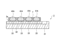
図1は、実施形態に係る半導体装置1の断面構造を概略的に示す図である。半導体装置1は、回路基板2及びこの回路基板2に実装された半導体光素子である光素子シリコンチップ3を備えた光モジュールである。本実施形態における光素子シリコンチップ3は、例えば、VCSEL(Vertical Cavity Semicondμctor Em
ission Laser)等の発光素子であり、発光部31や導波路(光伝送路)32
等を有している。また、回路基板2は、光素子シリコンチップ3の発光部31から出力された光を受光する受光部21や、受光部21によって受光した導波路(光伝送路)22等(図示省略)を備えている。半田バンプ4は、半田によって形成された突起電極である。回路基板2及び光素子シリコンチップ3は半田バンプ4を介して接合されている。回路基板2及び光素子シリコンチップ3は、それぞれ基板及び半導体素子の一例である。
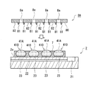
次に、光素子シリコンチップ3の実装方法について説明する。図2〜図11は、光素子シリコンチップ31の実装工程を説明する図である。
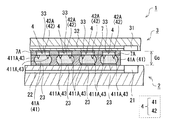
取り付けは、以下の手順で行うことができる。まず、基板側パッド23上にフラックスを供給する。基板側パッド23上へのフラックスの供給は、印刷装置を用いたスキージングによって行ってもよい。基板側パッド23に対するフラックスの塗布が終わると、フラックス上に高融点半田ボール41Aを搭載し、リフロー炉によって加熱(リフロー)を行う。ここでのリフロー温度は、高融点半田ボール41Aの溶融温度よりも高い温度(例えば、235℃程度)としてもよい。リフローを行うことにより、高融点半田ボール41Aが溶融し、各基板側パッド23に対して高融点半田ボール41Aが一体に接合される。本実施形態において、高融点半田ボール41Aは、第1半田接合材料の一例である。
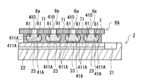
ルド樹脂7によって凹部411が覆われることを抑制することができる。以上のように、本実施形態では、高融点半田ボール41Aの頭頂部410を残して、高融点半田ボール41Aの周囲がモールド樹脂7によって被覆される。その後、モールド樹脂7を冷却することで硬化した後、高融点半田ボール41Aから凹部形成用治具6が取り外される。
を配置する。光素子シリコンチップ3の下面3aにおける適所には複数の素子側パッド33が露出形成されている。また、光素子シリコンチップ3には、発光部31や導波路32が形成されている。光素子シリコンチップ3は、素子側パッド33と基板側パッド23との平面位置が合致し、かつ、回路基板2と光素子シリコンチップ3との間に所定の接合ギャップGcが設けられるように、回路基板2との相対位置が調整される。
接合部43を形成することができる。このように、高融点半田接合部41及び低融点半田接合部42の接合境界面に凹凸接合部43を形成することで、高融点半田接合部41及び低融点半田接合部42相互の機械的噛み合い作用によって、外力に抵抗する機械的強度を大きくすることができる。
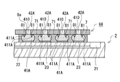
次に、光素子シリコンチップ3の実装方法の変形例について説明する。図12〜図18は、本変形例に係る光素子シリコンチップ3の実装工程を説明する図である。なお、以下では、図2〜図11を参照して説明した実装方法との相違点を中心に説明する。また、上述まで実施形態と共通する構成については同一の参照符号を付すことにより、その詳しい説明を省略する。
する(封止工程)。なお、封止工程において供給されたモールド樹脂7の上面は平坦になっていなくてもよい。
充填される。次に、図17に示すように、光素子シリコンチップ3の下面3aが回路基板2の上面2aと向き合うように光素子シリコンチップ3を配置する。光素子シリコンチップ3は、素子側パッド33と基板側パッド23との平面位置が合致し、かつ、回路基板2と光素子シリコンチップ3との間に所定の接合ギャップGcが設けられるように、回路基板2との相対位置が調整される。
でき、半導体装置1の製造効率を高めることができる。
2・・・回路基板
3・・・光素子シリコンチップ
4・・・半田バンプ
6・・・凹部形成用治具
7・・・モールド樹脂
23・・・基板側パッド
33・・・素子側パッド
41・・・高融点半田接合部
41A・・・高融点半田ボール
42・・・低融点半田接合部
42A・・・低融点半田ペースト
43・・・凹凸接合部
410・・・頭頂部
411・・・凹部
Gc・・・接合ギャップ
Claims (7)
- 基板に半導体素子を実装する実装方法であって、
前記基板に形成された基板側パッド上に第1半田接合材料を取り付ける工程と、
前記第1半田接合材料上に該第1半田接合材料よりも融点が低い第2半田接合材料を供給する工程と、
前記半導体素子に形成された素子側パッドが対応する前記基板側パッドに対向し、かつ、前記基板との間に所定の接合ギャップが設けられるように前記半導体素子を配置する工程と、
前記第1半田接合材料の融点よりも低温かつ前記第2半田接合材料の融点よりも高温のリフロー温度でリフローを行い、該第1半田接合材料及び第2半田接合材料を接合するリフロー工程と、
を有する、
半導体素子の実装方法。 - 前記第1半田接合材料の頭頂部に凹部を形成する凹部形成工程を更に有し、
前記第2半田接合材料を供給する工程においては、前記凹部に前記第2半田接合材料が充填されるように該第2半田接合材料を供給する、
請求項1に記載の半導体素子の実装方法。 - 前記第2半田接合材料を供給する前に、前記基板上に封止材料を供給し、少なくとも前記第1半田接合材料の頭頂部が露出するように該第1半田接合材料を封止する封止工程を、更に有する、
請求項2に記載の半導体素子の実装方法。 - 前記第2半田接合材料を供給する前に前記封止材料の上面を平坦にする平坦化工程、を更に有する、
請求項3に記載の半導体素子の実装方法。 - 前記封止工程を前記凹部形成工程の前に行う、
請求項3又は4に記載の半導体素子の実装方法。 - 前記凹部形成工程において、前記第1半田接合材料の頭頂部に所定の治具を押し付けることによって前記凹部を形成し、
前記封止工程において、前記頭頂部に前記治具を押し付けた状態で前記第1半田接合材料を封止する、
請求項3から5の何れか一項に記載の半導体素子の実装方法。 - 前記凹部形成工程において、前記第1半田接合材料の頭頂部を加熱しながら前記凹部を形成する、
請求項2から6の何れか一項に記載の半導体素子の実装方法。
Priority Applications (2)
| Application Number | Priority Date | Filing Date | Title |
|---|---|---|---|
| JP2013058764A JP6197319B2 (ja) | 2013-03-21 | 2013-03-21 | 半導体素子の実装方法 |
| US14/073,998 US9615464B2 (en) | 2013-03-21 | 2013-11-07 | Method of mounting semiconductor element, and semiconductor device |
Applications Claiming Priority (1)
| Application Number | Priority Date | Filing Date | Title |
|---|---|---|---|
| JP2013058764A JP6197319B2 (ja) | 2013-03-21 | 2013-03-21 | 半導体素子の実装方法 |
Publications (2)
| Publication Number | Publication Date |
|---|---|
| JP2014183301A JP2014183301A (ja) | 2014-09-29 |
| JP6197319B2 true JP6197319B2 (ja) | 2017-09-20 |
Family
ID=51568998
Family Applications (1)
| Application Number | Title | Priority Date | Filing Date |
|---|---|---|---|
| JP2013058764A Expired - Fee Related JP6197319B2 (ja) | 2013-03-21 | 2013-03-21 | 半導体素子の実装方法 |
Country Status (2)
| Country | Link |
|---|---|
| US (1) | US9615464B2 (ja) |
| JP (1) | JP6197319B2 (ja) |
Families Citing this family (11)
| Publication number | Priority date | Publication date | Assignee | Title |
|---|---|---|---|---|
| WO2012090901A1 (ja) * | 2010-12-28 | 2012-07-05 | 京セラ株式会社 | 光モジュールおよび光配線基板 |
| WO2014061085A1 (ja) * | 2012-10-15 | 2014-04-24 | 千住金属工業株式会社 | 低温ソルダペーストのはんだ付け方法 |
| JP6307131B2 (ja) * | 2015-09-08 | 2018-04-04 | エルジー エレクトロニクス インコーポレイティド | 太陽電池モジュール及びその製造方法 |
| CN109661726A (zh) * | 2017-01-20 | 2019-04-19 | 联想(新加坡)私人有限公司 | 钎焊接合方法和钎焊接头 |
| US10586782B2 (en) | 2017-07-01 | 2020-03-10 | International Business Machines Corporation | Lead-free solder joining of electronic structures |
| CN108346952B (zh) * | 2018-01-25 | 2020-11-24 | 番禺得意精密电子工业有限公司 | 电连接器固持装置 |
| CN110718524B (zh) * | 2019-08-30 | 2024-03-15 | 华为技术有限公司 | 电子组件及电子设备 |
| US11557878B2 (en) * | 2019-10-22 | 2023-01-17 | University Of Maryland, College Park | High power, narrow linewidth semiconductor laser system and method of fabrication |
| JP6767665B1 (ja) * | 2020-06-10 | 2020-10-14 | 千住金属工業株式会社 | バンプ電極基板の形成方法 |
| DE102021103360A1 (de) * | 2021-02-05 | 2022-08-11 | Few Fahrzeugelektrik Werk Gmbh & Co. Kg | Verfahren zur Herstellung einer Vorverzinnungsanordnung und derartige Vorverzinnungsanordnung |
| KR20230141813A (ko) * | 2021-02-10 | 2023-10-10 | 가부시끼가이샤 레조낙 | 땜납 범프 부착 부재의 제조 방법, 땜납 범프 부착 부재, 및 땜납 범프 형성용 부재 |
Family Cites Families (42)
| Publication number | Priority date | Publication date | Assignee | Title |
|---|---|---|---|---|
| DE3824865A1 (de) * | 1988-07-21 | 1990-01-25 | Productech Gmbh | Herstellen von loetflaechen |
| JP3049800B2 (ja) | 1991-02-28 | 2000-06-05 | 日本電気株式会社 | 半導体受光素子のバンプ電極形成方法 |
| US5203075A (en) * | 1991-08-12 | 1993-04-20 | Inernational Business Machines | Method of bonding flexible circuit to cicuitized substrate to provide electrical connection therebetween using different solders |
| US5545589A (en) * | 1993-01-28 | 1996-08-13 | Matsushita Electric Industrial Co., Ltd. | Method of forming a bump having a rugged side, a semiconductor device having the bump, and a method of mounting a semiconductor unit and a semiconductor device |
| US5477086A (en) * | 1993-04-30 | 1995-12-19 | Lsi Logic Corporation | Shaped, self-aligning micro-bump structures |
| US5470787A (en) * | 1994-05-02 | 1995-11-28 | Motorola, Inc. | Semiconductor device solder bump having intrinsic potential for forming an extended eutectic region and method for making and using the same |
| JPH0829638A (ja) * | 1994-05-12 | 1996-02-02 | Fujitsu Ltd | 光導波路・光ファイバ接続構造及び光導波路・光ファイバ接続方法並びに光導波路・光ファイバ接続に使用される光導波路基板及び同基板の製造方法並びに光導波路・光ファイバ接続に使用されるファイバ基板付き光ファイバ |
| JP3348528B2 (ja) * | 1994-07-20 | 2002-11-20 | 富士通株式会社 | 半導体装置の製造方法と半導体装置及び電子回路装置の製造方法と電子回路装置 |
| DE19511898C2 (de) * | 1995-03-31 | 1999-09-23 | Fraunhofer Ges Forschung | Verfahren zur Verbindung von Kontaktflächen eines elektronischen Bauelements und eines Substrats |
| US5889326A (en) * | 1996-02-27 | 1999-03-30 | Nec Corporation | Structure for bonding semiconductor device to substrate |
| JPH1013007A (ja) * | 1996-03-29 | 1998-01-16 | Ngk Spark Plug Co Ltd | 半田バンプを有する配線基板及びその製造方法及び平坦化治具 |
| JPH09275269A (ja) * | 1996-04-01 | 1997-10-21 | Omron Corp | 電子部品を回路基板に実装する方法,ならびにそれに用いる電子部品および回路基板 |
| JP3145331B2 (ja) * | 1996-04-26 | 2001-03-12 | 日本特殊陶業株式会社 | 中継基板、その製造方法、基板と中継基板と取付基板とからなる構造体、基板と中継基板の接続体および中継基板と取付基板の接続体の製造方法 |
| JP3180041B2 (ja) * | 1996-10-09 | 2001-06-25 | 住友金属工業株式会社 | 接続端子及びその形成方法 |
| US5872400A (en) * | 1997-06-25 | 1999-02-16 | International Business Machines Corporation | High melting point solder ball coated with a low melting point solder |
| US5984164A (en) * | 1997-10-31 | 1999-11-16 | Micron Technology, Inc. | Method of using an electrically conductive elevation shaping tool |
| DE19750073A1 (de) * | 1997-11-12 | 1999-05-20 | Bosch Gmbh Robert | Schaltungsträgerplatte |
| JP3344956B2 (ja) * | 1998-01-08 | 2002-11-18 | 日本特殊陶業株式会社 | 積層セラミック基板の製造方法 |
| US6046910A (en) * | 1998-03-18 | 2000-04-04 | Motorola, Inc. | Microelectronic assembly having slidable contacts and method for manufacturing the assembly |
| JP3975569B2 (ja) * | 1998-09-01 | 2007-09-12 | ソニー株式会社 | 実装基板及びその製造方法 |
| US6225206B1 (en) * | 1999-05-10 | 2001-05-01 | International Business Machines Corporation | Flip chip C4 extension structure and process |
| US6267650B1 (en) * | 1999-08-09 | 2001-07-31 | Micron Technology, Inc. | Apparatus and methods for substantial planarization of solder bumps |
| JP2001085470A (ja) * | 1999-09-16 | 2001-03-30 | Fujitsu Ltd | 半導体装置及びその製造方法 |
| US6683387B1 (en) * | 2000-06-15 | 2004-01-27 | Advanced Micro Devices, Inc. | Flip chip carrier package with adapted landing pads |
| JP4609617B2 (ja) * | 2000-08-01 | 2011-01-12 | 日本電気株式会社 | 半導体装置の実装方法及び実装構造体 |
| US7414319B2 (en) * | 2000-10-13 | 2008-08-19 | Bridge Semiconductor Corporation | Semiconductor chip assembly with metal containment wall and solder terminal |
| JP2002190497A (ja) * | 2000-12-21 | 2002-07-05 | Sony Corp | フリップチップ実装用の封止樹脂 |
| JP4131623B2 (ja) | 2001-09-12 | 2008-08-13 | 三洋電機株式会社 | 電極構造およびその製造方法 |
| US6583517B1 (en) * | 2002-04-09 | 2003-06-24 | International Business Machines Corporation | Method and structure for joining two substrates with a low melt solder joint |
| JP2004012803A (ja) * | 2002-06-06 | 2004-01-15 | Fujitsu Ltd | 光伝送用プリント板ユニット及び実装方法 |
| JP2004103928A (ja) * | 2002-09-11 | 2004-04-02 | Fujitsu Ltd | 基板及びハンダボールの形成方法及びその実装構造 |
| JP3905100B2 (ja) * | 2004-08-13 | 2007-04-18 | 株式会社東芝 | 半導体装置とその製造方法 |
| US7611040B2 (en) * | 2005-05-24 | 2009-11-03 | Panasonic Corporation | Method for forming solder bump and method for mounting semiconductor device using a solder powder resin composition |
| JP4251458B2 (ja) * | 2005-12-21 | 2009-04-08 | Tdk株式会社 | チップ部品の実装方法及び回路基板 |
| JP2008071792A (ja) * | 2006-09-12 | 2008-03-27 | Toshiba Corp | 半導体装置の製造方法 |
| JP5066935B2 (ja) * | 2007-02-22 | 2012-11-07 | 富士通株式会社 | 電子部品および電子装置の製造方法 |
| US8390117B2 (en) * | 2007-12-11 | 2013-03-05 | Panasonic Corporation | Semiconductor device and method of manufacturing the same |
| WO2010061428A1 (ja) * | 2008-11-28 | 2010-06-03 | 富士通株式会社 | 電子装置の製造方法、電子部品搭載用基板及びその製造方法 |
| JP5800674B2 (ja) * | 2011-10-25 | 2015-10-28 | 日本特殊陶業株式会社 | 配線基板及びその製造方法 |
| JP2013093405A (ja) * | 2011-10-25 | 2013-05-16 | Ngk Spark Plug Co Ltd | 配線基板及びその製造方法 |
| US8828860B2 (en) * | 2012-08-30 | 2014-09-09 | International Business Machines Corporation | Double solder bumps on substrates for low temperature flip chip bonding |
| US8920934B2 (en) * | 2013-03-29 | 2014-12-30 | Intel Corporation | Hybrid solder and filled paste in microelectronic packaging |
-
2013
- 2013-03-21 JP JP2013058764A patent/JP6197319B2/ja not_active Expired - Fee Related
- 2013-11-07 US US14/073,998 patent/US9615464B2/en not_active Expired - Fee Related
Also Published As
| Publication number | Publication date |
|---|---|
| US20140285989A1 (en) | 2014-09-25 |
| US9615464B2 (en) | 2017-04-04 |
| JP2014183301A (ja) | 2014-09-29 |
Similar Documents
| Publication | Publication Date | Title |
|---|---|---|
| JP6197319B2 (ja) | 半導体素子の実装方法 | |
| CN101996902B (zh) | 半导体器件的制造方法 | |
| JP4928945B2 (ja) | バンプ−オン−リードフリップチップ相互接続 | |
| JP5120342B2 (ja) | 半導体パッケージの製造方法 | |
| JP4907500B2 (ja) | 導電性バンプの形成方法 | |
| TWI397978B (zh) | 晶片結構及其製程與覆晶封裝結構及其製程 | |
| JP5160390B2 (ja) | リードピン付配線基板及びその製造方法 | |
| JP5422830B2 (ja) | リードピン付配線基板及びその製造方法 | |
| CN107078118A (zh) | 插入器到封装基板的耦合 | |
| JP2010123676A (ja) | 半導体装置の製造方法、半導体装置 | |
| JP5889160B2 (ja) | 電子機器の製造方法 | |
| CN112908873A (zh) | 半导体组件组装方法、半导体组件和电子设备 | |
| JP6877271B2 (ja) | 光モジュールの製造方法 | |
| JP5212392B2 (ja) | 半導体装置 | |
| JP2006351935A (ja) | 半導体チップ実装基板及びそれを用いた半導体装置 | |
| JP2007243106A (ja) | 半導体パッケージ構造 | |
| JP4200090B2 (ja) | 半導体装置の製造方法 | |
| JP4952527B2 (ja) | 半導体装置の製造方法及び半導体装置 | |
| CN100542380C (zh) | 电子零部件安装方法及其使用的电路板和电路板单元 | |
| JP2009110991A (ja) | 半導体装置及びその製造方法 | |
| JP2007258448A (ja) | 半導体装置 | |
| JP2008192833A (ja) | 半導体装置の製造方法 | |
| JP5576053B2 (ja) | 半導体装置の製造方法、及び回路基板シート | |
| TWI803127B (zh) | 半導體元件組裝方法、半導體元件和電子設備 | |
| JP4752717B2 (ja) | モジュールの製造方法 |
Legal Events
| Date | Code | Title | Description |
|---|---|---|---|
| A621 | Written request for application examination |
Free format text: JAPANESE INTERMEDIATE CODE: A621 Effective date: 20151106 |
|
| A977 | Report on retrieval |
Free format text: JAPANESE INTERMEDIATE CODE: A971007 Effective date: 20160907 |
|
| A131 | Notification of reasons for refusal |
Free format text: JAPANESE INTERMEDIATE CODE: A131 Effective date: 20161004 |
|
| A521 | Request for written amendment filed |
Free format text: JAPANESE INTERMEDIATE CODE: A523 Effective date: 20161130 |
|
| A131 | Notification of reasons for refusal |
Free format text: JAPANESE INTERMEDIATE CODE: A131 Effective date: 20170509 |
|
| A521 | Request for written amendment filed |
Free format text: JAPANESE INTERMEDIATE CODE: A523 Effective date: 20170630 |
|
| TRDD | Decision of grant or rejection written | ||
| A01 | Written decision to grant a patent or to grant a registration (utility model) |
Free format text: JAPANESE INTERMEDIATE CODE: A01 Effective date: 20170725 |
|
| A61 | First payment of annual fees (during grant procedure) |
Free format text: JAPANESE INTERMEDIATE CODE: A61 Effective date: 20170807 |
|
| R150 | Certificate of patent or registration of utility model |
Ref document number: 6197319 Country of ref document: JP Free format text: JAPANESE INTERMEDIATE CODE: R150 |
|
| LAPS | Cancellation because of no payment of annual fees |