JP5577075B2 - Semiconductor device - Google Patents
Semiconductor device Download PDFInfo
- Publication number
- JP5577075B2 JP5577075B2 JP2009258516A JP2009258516A JP5577075B2 JP 5577075 B2 JP5577075 B2 JP 5577075B2 JP 2009258516 A JP2009258516 A JP 2009258516A JP 2009258516 A JP2009258516 A JP 2009258516A JP 5577075 B2 JP5577075 B2 JP 5577075B2
- Authority
- JP
- Japan
- Prior art keywords
- layer
- electrode
- oxide semiconductor
- transistor
- tft
- Prior art date
- Legal status (The legal status is an assumption and is not a legal conclusion. Google has not performed a legal analysis and makes no representation as to the accuracy of the status listed.)
- Expired - Fee Related
Links
- 239000004065 semiconductor Substances 0.000 title claims description 198
- 238000000034 method Methods 0.000 claims description 52
- 230000008569 process Effects 0.000 claims description 15
- 239000004020 conductor Substances 0.000 claims description 10
- 238000012545 processing Methods 0.000 claims description 2
- 239000010410 layer Substances 0.000 description 412
- 239000010408 film Substances 0.000 description 221
- 239000010409 thin film Substances 0.000 description 146
- 239000000758 substrate Substances 0.000 description 88
- 239000000463 material Substances 0.000 description 56
- 239000004973 liquid crystal related substance Substances 0.000 description 48
- 230000001681 protective effect Effects 0.000 description 34
- 239000003990 capacitor Substances 0.000 description 33
- 238000004519 manufacturing process Methods 0.000 description 31
- 230000006870 function Effects 0.000 description 27
- 239000013078 crystal Substances 0.000 description 26
- 229910052782 aluminium Inorganic materials 0.000 description 24
- XAGFODPZIPBFFR-UHFFFAOYSA-N aluminium Chemical compound [Al] XAGFODPZIPBFFR-UHFFFAOYSA-N 0.000 description 22
- 239000010936 titanium Substances 0.000 description 19
- 229910007541 Zn O Inorganic materials 0.000 description 18
- 230000015572 biosynthetic process Effects 0.000 description 18
- 238000004544 sputter deposition Methods 0.000 description 18
- 238000005530 etching Methods 0.000 description 16
- 239000011159 matrix material Substances 0.000 description 16
- 238000000206 photolithography Methods 0.000 description 16
- 102100040862 Dual specificity protein kinase CLK1 Human genes 0.000 description 13
- 239000011521 glass Substances 0.000 description 13
- 239000000956 alloy Substances 0.000 description 12
- XLOMVQKBTHCTTD-UHFFFAOYSA-N Zinc monoxide Chemical compound [Zn]=O XLOMVQKBTHCTTD-UHFFFAOYSA-N 0.000 description 11
- 229910045601 alloy Inorganic materials 0.000 description 11
- 238000004891 communication Methods 0.000 description 11
- 239000010949 copper Substances 0.000 description 11
- 238000010586 diagram Methods 0.000 description 11
- 229920005989 resin Polymers 0.000 description 11
- 239000011347 resin Substances 0.000 description 11
- 239000000565 sealant Substances 0.000 description 11
- 239000002356 single layer Substances 0.000 description 11
- 229910052581 Si3N4 Inorganic materials 0.000 description 10
- 239000011651 chromium Substances 0.000 description 10
- 230000009977 dual effect Effects 0.000 description 10
- 229910052751 metal Inorganic materials 0.000 description 10
- HQVNEWCFYHHQES-UHFFFAOYSA-N silicon nitride Chemical compound N12[Si]34N5[Si]62N3[Si]51N64 HQVNEWCFYHHQES-UHFFFAOYSA-N 0.000 description 10
- 229910052719 titanium Inorganic materials 0.000 description 10
- 229910052750 molybdenum Inorganic materials 0.000 description 9
- XKRFYHLGVUSROY-UHFFFAOYSA-N Argon Chemical compound [Ar] XKRFYHLGVUSROY-UHFFFAOYSA-N 0.000 description 8
- ZOKXTWBITQBERF-UHFFFAOYSA-N Molybdenum Chemical compound [Mo] ZOKXTWBITQBERF-UHFFFAOYSA-N 0.000 description 8
- VYPSYNLAJGMNEJ-UHFFFAOYSA-N Silicium dioxide Chemical compound O=[Si]=O VYPSYNLAJGMNEJ-UHFFFAOYSA-N 0.000 description 8
- XUIMIQQOPSSXEZ-UHFFFAOYSA-N Silicon Chemical compound [Si] XUIMIQQOPSSXEZ-UHFFFAOYSA-N 0.000 description 8
- RTAQQCXQSZGOHL-UHFFFAOYSA-N Titanium Chemical compound [Ti] RTAQQCXQSZGOHL-UHFFFAOYSA-N 0.000 description 8
- 239000012298 atmosphere Substances 0.000 description 8
- 239000002184 metal Substances 0.000 description 8
- 239000011733 molybdenum Substances 0.000 description 8
- 229910052710 silicon Inorganic materials 0.000 description 8
- 239000010703 silicon Substances 0.000 description 8
- 229910052814 silicon oxide Inorganic materials 0.000 description 8
- 238000003860 storage Methods 0.000 description 8
- 229910052721 tungsten Inorganic materials 0.000 description 8
- RYGMFSIKBFXOCR-UHFFFAOYSA-N Copper Chemical compound [Cu] RYGMFSIKBFXOCR-UHFFFAOYSA-N 0.000 description 7
- 101000749294 Homo sapiens Dual specificity protein kinase CLK1 Proteins 0.000 description 7
- 229910052802 copper Inorganic materials 0.000 description 7
- AMGQUBHHOARCQH-UHFFFAOYSA-N indium;oxotin Chemical compound [In].[Sn]=O AMGQUBHHOARCQH-UHFFFAOYSA-N 0.000 description 7
- 239000010937 tungsten Substances 0.000 description 7
- 238000001039 wet etching Methods 0.000 description 7
- 229910052804 chromium Inorganic materials 0.000 description 6
- 230000003287 optical effect Effects 0.000 description 6
- 229910052715 tantalum Inorganic materials 0.000 description 6
- 238000012360 testing method Methods 0.000 description 6
- WFKWXMTUELFFGS-UHFFFAOYSA-N tungsten Chemical compound [W] WFKWXMTUELFFGS-UHFFFAOYSA-N 0.000 description 6
- 239000011787 zinc oxide Substances 0.000 description 6
- VYZAMTAEIAYCRO-UHFFFAOYSA-N Chromium Chemical compound [Cr] VYZAMTAEIAYCRO-UHFFFAOYSA-N 0.000 description 5
- 102100040844 Dual specificity protein kinase CLK2 Human genes 0.000 description 5
- 102100040858 Dual specificity protein kinase CLK4 Human genes 0.000 description 5
- 101000749291 Homo sapiens Dual specificity protein kinase CLK2 Proteins 0.000 description 5
- 101000749298 Homo sapiens Dual specificity protein kinase CLK4 Proteins 0.000 description 5
- 229910052779 Neodymium Inorganic materials 0.000 description 5
- 229910052786 argon Inorganic materials 0.000 description 5
- 239000000945 filler Substances 0.000 description 5
- 239000012535 impurity Substances 0.000 description 5
- 229910003437 indium oxide Inorganic materials 0.000 description 5
- PJXISJQVUVHSOJ-UHFFFAOYSA-N indium(iii) oxide Chemical compound [O-2].[O-2].[O-2].[In+3].[In+3] PJXISJQVUVHSOJ-UHFFFAOYSA-N 0.000 description 5
- 239000007788 liquid Substances 0.000 description 5
- 239000007769 metal material Substances 0.000 description 5
- 239000000203 mixture Substances 0.000 description 5
- QEFYFXOXNSNQGX-UHFFFAOYSA-N neodymium atom Chemical compound [Nd] QEFYFXOXNSNQGX-UHFFFAOYSA-N 0.000 description 5
- 239000001301 oxygen Substances 0.000 description 5
- 229910052760 oxygen Inorganic materials 0.000 description 5
- 239000002245 particle Substances 0.000 description 5
- 238000009832 plasma treatment Methods 0.000 description 5
- 229910052706 scandium Inorganic materials 0.000 description 5
- SIXSYDAISGFNSX-UHFFFAOYSA-N scandium atom Chemical compound [Sc] SIXSYDAISGFNSX-UHFFFAOYSA-N 0.000 description 5
- 239000012798 spherical particle Substances 0.000 description 5
- GUVRBAGPIYLISA-UHFFFAOYSA-N tantalum atom Chemical compound [Ta] GUVRBAGPIYLISA-UHFFFAOYSA-N 0.000 description 5
- QGZKDVFQNNGYKY-UHFFFAOYSA-N Ammonia Chemical compound N QGZKDVFQNNGYKY-UHFFFAOYSA-N 0.000 description 4
- 102100040856 Dual specificity protein kinase CLK3 Human genes 0.000 description 4
- 101000749304 Homo sapiens Dual specificity protein kinase CLK3 Proteins 0.000 description 4
- GWEVSGVZZGPLCZ-UHFFFAOYSA-N Titan oxide Chemical compound O=[Ti]=O GWEVSGVZZGPLCZ-UHFFFAOYSA-N 0.000 description 4
- 230000001413 cellular effect Effects 0.000 description 4
- 229920001940 conductive polymer Polymers 0.000 description 4
- PMHQVHHXPFUNSP-UHFFFAOYSA-M copper(1+);methylsulfanylmethane;bromide Chemical compound Br[Cu].CSC PMHQVHHXPFUNSP-UHFFFAOYSA-M 0.000 description 4
- KPUWHANPEXNPJT-UHFFFAOYSA-N disiloxane Chemical class [SiH3]O[SiH3] KPUWHANPEXNPJT-UHFFFAOYSA-N 0.000 description 4
- 229910052733 gallium Inorganic materials 0.000 description 4
- 238000010438 heat treatment Methods 0.000 description 4
- 230000007246 mechanism Effects 0.000 description 4
- QGLKJKCYBOYXKC-UHFFFAOYSA-N nonaoxidotritungsten Chemical compound O=[W]1(=O)O[W](=O)(=O)O[W](=O)(=O)O1 QGLKJKCYBOYXKC-UHFFFAOYSA-N 0.000 description 4
- 230000003071 parasitic effect Effects 0.000 description 4
- 238000005192 partition Methods 0.000 description 4
- 229920003023 plastic Polymers 0.000 description 4
- 239000004033 plastic Substances 0.000 description 4
- OGIDPMRJRNCKJF-UHFFFAOYSA-N titanium oxide Inorganic materials [Ti]=O OGIDPMRJRNCKJF-UHFFFAOYSA-N 0.000 description 4
- 229910001930 tungsten oxide Inorganic materials 0.000 description 4
- YVTHLONGBIQYBO-UHFFFAOYSA-N zinc indium(3+) oxygen(2-) Chemical compound [O--].[Zn++].[In+3] YVTHLONGBIQYBO-UHFFFAOYSA-N 0.000 description 4
- QTBSBXVTEAMEQO-UHFFFAOYSA-N Acetic acid Chemical compound CC(O)=O QTBSBXVTEAMEQO-UHFFFAOYSA-N 0.000 description 3
- 229910005191 Ga 2 O 3 Inorganic materials 0.000 description 3
- 201000005569 Gout Diseases 0.000 description 3
- DGAQECJNVWCQMB-PUAWFVPOSA-M Ilexoside XXIX Chemical compound C[C@@H]1CC[C@@]2(CC[C@@]3(C(=CC[C@H]4[C@]3(CC[C@@H]5[C@@]4(CC[C@@H](C5(C)C)OS(=O)(=O)[O-])C)C)[C@@H]2[C@]1(C)O)C)C(=O)O[C@H]6[C@@H]([C@H]([C@@H]([C@H](O6)CO)O)O)O.[Na+] DGAQECJNVWCQMB-PUAWFVPOSA-M 0.000 description 3
- NRTOMJZYCJJWKI-UHFFFAOYSA-N Titanium nitride Chemical compound [Ti]#N NRTOMJZYCJJWKI-UHFFFAOYSA-N 0.000 description 3
- NIXOWILDQLNWCW-UHFFFAOYSA-N acrylic acid group Chemical group C(C=C)(=O)O NIXOWILDQLNWCW-UHFFFAOYSA-N 0.000 description 3
- 229910021417 amorphous silicon Inorganic materials 0.000 description 3
- QVGXLLKOCUKJST-UHFFFAOYSA-N atomic oxygen Chemical compound [O] QVGXLLKOCUKJST-UHFFFAOYSA-N 0.000 description 3
- 239000000969 carrier Substances 0.000 description 3
- 239000000428 dust Substances 0.000 description 3
- 230000005611 electricity Effects 0.000 description 3
- 238000005401 electroluminescence Methods 0.000 description 3
- 230000005669 field effect Effects 0.000 description 3
- 239000007789 gas Substances 0.000 description 3
- 238000003780 insertion Methods 0.000 description 3
- 230000037431 insertion Effects 0.000 description 3
- 238000009413 insulation Methods 0.000 description 3
- 229910052742 iron Inorganic materials 0.000 description 3
- 229910052759 nickel Inorganic materials 0.000 description 3
- 150000002894 organic compounds Chemical class 0.000 description 3
- TWNQGVIAIRXVLR-UHFFFAOYSA-N oxo(oxoalumanyloxy)alumane Chemical compound O=[Al]O[Al]=O TWNQGVIAIRXVLR-UHFFFAOYSA-N 0.000 description 3
- 229910021420 polycrystalline silicon Inorganic materials 0.000 description 3
- 229920006267 polyester film Polymers 0.000 description 3
- 229920002620 polyvinyl fluoride Polymers 0.000 description 3
- 229910052708 sodium Inorganic materials 0.000 description 3
- 239000011734 sodium Substances 0.000 description 3
- 238000004528 spin coating Methods 0.000 description 3
- 230000003068 static effect Effects 0.000 description 3
- -1 tungsten nitride Chemical class 0.000 description 3
- UWCWUCKPEYNDNV-LBPRGKRZSA-N 2,6-dimethyl-n-[[(2s)-pyrrolidin-2-yl]methyl]aniline Chemical compound CC1=CC=CC(C)=C1NC[C@H]1NCCC1 UWCWUCKPEYNDNV-LBPRGKRZSA-N 0.000 description 2
- IJGRMHOSHXDMSA-UHFFFAOYSA-N Atomic nitrogen Chemical compound N#N IJGRMHOSHXDMSA-UHFFFAOYSA-N 0.000 description 2
- CURLTUGMZLYLDI-UHFFFAOYSA-N Carbon dioxide Chemical compound O=C=O CURLTUGMZLYLDI-UHFFFAOYSA-N 0.000 description 2
- VEXZGXHMUGYJMC-UHFFFAOYSA-N Hydrochloric acid Chemical compound Cl VEXZGXHMUGYJMC-UHFFFAOYSA-N 0.000 description 2
- MHAJPDPJQMAIIY-UHFFFAOYSA-N Hydrogen peroxide Chemical compound OO MHAJPDPJQMAIIY-UHFFFAOYSA-N 0.000 description 2
- NBIIXXVUZAFLBC-UHFFFAOYSA-N Phosphoric acid Chemical compound OP(O)(O)=O NBIIXXVUZAFLBC-UHFFFAOYSA-N 0.000 description 2
- 239000004642 Polyimide Substances 0.000 description 2
- 229910021529 ammonia Inorganic materials 0.000 description 2
- DQXBYHZEEUGOBF-UHFFFAOYSA-N but-3-enoic acid;ethene Chemical compound C=C.OC(=O)CC=C DQXBYHZEEUGOBF-UHFFFAOYSA-N 0.000 description 2
- 230000008859 change Effects 0.000 description 2
- 230000000593 degrading effect Effects 0.000 description 2
- 238000000151 deposition Methods 0.000 description 2
- 230000008021 deposition Effects 0.000 description 2
- 238000009792 diffusion process Methods 0.000 description 2
- 238000001312 dry etching Methods 0.000 description 2
- 239000005038 ethylene vinyl acetate Substances 0.000 description 2
- 230000005281 excited state Effects 0.000 description 2
- 230000001747 exhibiting effect Effects 0.000 description 2
- 239000000284 extract Substances 0.000 description 2
- 230000002349 favourable effect Effects 0.000 description 2
- 239000005262 ferroelectric liquid crystals (FLCs) Substances 0.000 description 2
- 239000011152 fibreglass Substances 0.000 description 2
- 238000007667 floating Methods 0.000 description 2
- 125000001153 fluoro group Chemical group F* 0.000 description 2
- 238000002347 injection Methods 0.000 description 2
- 239000007924 injection Substances 0.000 description 2
- 239000003094 microcapsule Substances 0.000 description 2
- 239000011859 microparticle Substances 0.000 description 2
- 125000000962 organic group Chemical group 0.000 description 2
- 239000011368 organic material Substances 0.000 description 2
- BPUBBGLMJRNUCC-UHFFFAOYSA-N oxygen(2-);tantalum(5+) Chemical compound [O-2].[O-2].[O-2].[O-2].[O-2].[Ta+5].[Ta+5] BPUBBGLMJRNUCC-UHFFFAOYSA-N 0.000 description 2
- 230000002093 peripheral effect Effects 0.000 description 2
- 229920001200 poly(ethylene-vinyl acetate) Polymers 0.000 description 2
- 229920002037 poly(vinyl butyral) polymer Polymers 0.000 description 2
- 229920001721 polyimide Polymers 0.000 description 2
- 229920000915 polyvinyl chloride Polymers 0.000 description 2
- 239000004800 polyvinyl chloride Substances 0.000 description 2
- 230000004044 response Effects 0.000 description 2
- 238000007650 screen-printing Methods 0.000 description 2
- 238000009751 slip forming Methods 0.000 description 2
- 239000000243 solution Substances 0.000 description 2
- 125000006850 spacer group Chemical group 0.000 description 2
- 239000000126 substance Substances 0.000 description 2
- 229910001936 tantalum oxide Inorganic materials 0.000 description 2
- 230000007704 transition Effects 0.000 description 2
- 229910052723 transition metal Inorganic materials 0.000 description 2
- 238000001771 vacuum deposition Methods 0.000 description 2
- 210000003462 vein Anatomy 0.000 description 2
- XLYOFNOQVPJJNP-UHFFFAOYSA-N water Substances O XLYOFNOQVPJJNP-UHFFFAOYSA-N 0.000 description 2
- 239000011701 zinc Substances 0.000 description 2
- 239000004925 Acrylic resin Substances 0.000 description 1
- 229920000178 Acrylic resin Polymers 0.000 description 1
- 229910017073 AlLi Inorganic materials 0.000 description 1
- 101100328957 Caenorhabditis elegans clk-1 gene Proteins 0.000 description 1
- 239000004986 Cholesteric liquid crystals (ChLC) Substances 0.000 description 1
- 239000004593 Epoxy Substances 0.000 description 1
- GYHNNYVSQQEPJS-UHFFFAOYSA-N Gallium Chemical compound [Ga] GYHNNYVSQQEPJS-UHFFFAOYSA-N 0.000 description 1
- 206010052128 Glare Diseases 0.000 description 1
- GRYLNZFGIOXLOG-UHFFFAOYSA-N Nitric acid Chemical compound O[N+]([O-])=O GRYLNZFGIOXLOG-UHFFFAOYSA-N 0.000 description 1
- OAICVXFJPJFONN-UHFFFAOYSA-N Phosphorus Chemical compound [P] OAICVXFJPJFONN-UHFFFAOYSA-N 0.000 description 1
- 239000004952 Polyamide Substances 0.000 description 1
- 229910002808 Si–O–Si Inorganic materials 0.000 description 1
- 229910006404 SnO 2 Inorganic materials 0.000 description 1
- 206010047571 Visual impairment Diseases 0.000 description 1
- 238000002441 X-ray diffraction Methods 0.000 description 1
- HCHKCACWOHOZIP-UHFFFAOYSA-N Zinc Chemical compound [Zn] HCHKCACWOHOZIP-UHFFFAOYSA-N 0.000 description 1
- GDFCWFBWQUEQIJ-UHFFFAOYSA-N [B].[P] Chemical compound [B].[P] GDFCWFBWQUEQIJ-UHFFFAOYSA-N 0.000 description 1
- 238000010521 absorption reaction Methods 0.000 description 1
- 230000001133 acceleration Effects 0.000 description 1
- 230000009471 action Effects 0.000 description 1
- 125000000217 alkyl group Chemical group 0.000 description 1
- 229910000147 aluminium phosphate Inorganic materials 0.000 description 1
- 239000005407 aluminoborosilicate glass Substances 0.000 description 1
- 238000000137 annealing Methods 0.000 description 1
- 125000003118 aryl group Chemical group 0.000 description 1
- 229910052788 barium Inorganic materials 0.000 description 1
- DSAJWYNOEDNPEQ-UHFFFAOYSA-N barium atom Chemical compound [Ba] DSAJWYNOEDNPEQ-UHFFFAOYSA-N 0.000 description 1
- 230000004888 barrier function Effects 0.000 description 1
- 230000008901 benefit Effects 0.000 description 1
- UMIVXZPTRXBADB-UHFFFAOYSA-N benzocyclobutene Chemical compound C1=CC=C2CCC2=C1 UMIVXZPTRXBADB-UHFFFAOYSA-N 0.000 description 1
- 230000002457 bidirectional effect Effects 0.000 description 1
- 239000011230 binding agent Substances 0.000 description 1
- 239000005380 borophosphosilicate glass Substances 0.000 description 1
- 239000005388 borosilicate glass Substances 0.000 description 1
- 239000001569 carbon dioxide Substances 0.000 description 1
- 229910002092 carbon dioxide Inorganic materials 0.000 description 1
- 239000000919 ceramic Substances 0.000 description 1
- 230000003098 cholesteric effect Effects 0.000 description 1
- 239000011248 coating agent Substances 0.000 description 1
- 238000000576 coating method Methods 0.000 description 1
- 238000004040 coloring Methods 0.000 description 1
- 239000000356 contaminant Substances 0.000 description 1
- 238000011109 contamination Methods 0.000 description 1
- 239000002872 contrast media Substances 0.000 description 1
- 229920001577 copolymer Polymers 0.000 description 1
- 238000002425 crystallisation Methods 0.000 description 1
- 230000008025 crystallization Effects 0.000 description 1
- 238000007872 degassing Methods 0.000 description 1
- 238000013461 design Methods 0.000 description 1
- 238000001514 detection method Methods 0.000 description 1
- 239000003989 dielectric material Substances 0.000 description 1
- 230000000694 effects Effects 0.000 description 1
- 230000005684 electric field Effects 0.000 description 1
- 238000005516 engineering process Methods 0.000 description 1
- 239000003822 epoxy resin Substances 0.000 description 1
- 239000011888 foil Substances 0.000 description 1
- 230000005283 ground state Effects 0.000 description 1
- 230000005525 hole transport Effects 0.000 description 1
- 239000001257 hydrogen Substances 0.000 description 1
- 229910052739 hydrogen Inorganic materials 0.000 description 1
- 125000004435 hydrogen atom Chemical class [H]* 0.000 description 1
- 229910052738 indium Inorganic materials 0.000 description 1
- APFVFJFRJDLVQX-UHFFFAOYSA-N indium atom Chemical compound [In] APFVFJFRJDLVQX-UHFFFAOYSA-N 0.000 description 1
- 239000011261 inert gas Substances 0.000 description 1
- 150000002484 inorganic compounds Chemical class 0.000 description 1
- 229910010272 inorganic material Inorganic materials 0.000 description 1
- 150000002500 ions Chemical class 0.000 description 1
- 238000003475 lamination Methods 0.000 description 1
- 238000005224 laser annealing Methods 0.000 description 1
- 229910052748 manganese Inorganic materials 0.000 description 1
- 239000012528 membrane Substances 0.000 description 1
- 229910021645 metal ion Inorganic materials 0.000 description 1
- 239000011259 mixed solution Substances 0.000 description 1
- 238000012986 modification Methods 0.000 description 1
- 230000004048 modification Effects 0.000 description 1
- 229910017604 nitric acid Inorganic materials 0.000 description 1
- 150000004767 nitrides Chemical class 0.000 description 1
- 229910052757 nitrogen Inorganic materials 0.000 description 1
- 239000012299 nitrogen atmosphere Substances 0.000 description 1
- 238000007645 offset printing Methods 0.000 description 1
- 239000012788 optical film Substances 0.000 description 1
- AHLBNYSZXLDEJQ-FWEHEUNISA-N orlistat Chemical compound CCCCCCCCCCC[C@H](OC(=O)[C@H](CC(C)C)NC=O)C[C@@H]1OC(=O)[C@H]1CCCCCC AHLBNYSZXLDEJQ-FWEHEUNISA-N 0.000 description 1
- 230000003647 oxidation Effects 0.000 description 1
- 238000007254 oxidation reaction Methods 0.000 description 1
- 229910052698 phosphorus Inorganic materials 0.000 description 1
- 239000011574 phosphorus Substances 0.000 description 1
- 239000000049 pigment Substances 0.000 description 1
- 229920002647 polyamide Polymers 0.000 description 1
- 229920000767 polyaniline Polymers 0.000 description 1
- 229920000647 polyepoxide Polymers 0.000 description 1
- 229920000128 polypyrrole Polymers 0.000 description 1
- 229920001296 polysiloxane Polymers 0.000 description 1
- 229920000123 polythiophene Polymers 0.000 description 1
- 239000011241 protective layer Substances 0.000 description 1
- 238000005546 reactive sputtering Methods 0.000 description 1
- 238000005215 recombination Methods 0.000 description 1
- 230000006798 recombination Effects 0.000 description 1
- 230000009467 reduction Effects 0.000 description 1
- 230000002441 reversible effect Effects 0.000 description 1
- 239000003566 sealing material Substances 0.000 description 1
- 238000005507 spraying Methods 0.000 description 1
- 239000010935 stainless steel Substances 0.000 description 1
- 229910001220 stainless steel Inorganic materials 0.000 description 1
- 239000007858 starting material Substances 0.000 description 1
- 125000001424 substituent group Chemical group 0.000 description 1
- 230000001360 synchronised effect Effects 0.000 description 1
- MZLGASXMSKOWSE-UHFFFAOYSA-N tantalum nitride Chemical compound [Ta]#N MZLGASXMSKOWSE-UHFFFAOYSA-N 0.000 description 1
- 229920001187 thermosetting polymer Polymers 0.000 description 1
- 150000003608 titanium Chemical class 0.000 description 1
- 229910000314 transition metal oxide Inorganic materials 0.000 description 1
- 150000003624 transition metals Chemical class 0.000 description 1
- 238000002834 transmittance Methods 0.000 description 1
- 239000002699 waste material Substances 0.000 description 1
- 229910052725 zinc Inorganic materials 0.000 description 1
- OYQCBJZGELKKPM-UHFFFAOYSA-N zinc indium(3+) oxygen(2-) Chemical compound [O-2].[Zn+2].[O-2].[In+3] OYQCBJZGELKKPM-UHFFFAOYSA-N 0.000 description 1
Images


Classifications
-
- H—ELECTRICITY
- H01—ELECTRIC ELEMENTS
- H01L—SEMICONDUCTOR DEVICES NOT COVERED BY CLASS H10
- H01L29/00—Semiconductor devices adapted for rectifying, amplifying, oscillating or switching, or capacitors or resistors with at least one potential-jump barrier or surface barrier, e.g. PN junction depletion layer or carrier concentration layer; Details of semiconductor bodies or of electrodes thereof ; Multistep manufacturing processes therefor
- H01L29/66—Types of semiconductor device ; Multistep manufacturing processes therefor
- H01L29/68—Types of semiconductor device ; Multistep manufacturing processes therefor controllable by only the electric current supplied, or only the electric potential applied, to an electrode which does not carry the current to be rectified, amplified or switched
- H01L29/76—Unipolar devices, e.g. field effect transistors
- H01L29/772—Field effect transistors
- H01L29/78—Field effect transistors with field effect produced by an insulated gate
- H01L29/786—Thin film transistors, i.e. transistors with a channel being at least partly a thin film
- H01L29/78645—Thin film transistors, i.e. transistors with a channel being at least partly a thin film with multiple gate
- H01L29/78648—Thin film transistors, i.e. transistors with a channel being at least partly a thin film with multiple gate arranged on opposing sides of the channel
-
- H—ELECTRICITY
- H01—ELECTRIC ELEMENTS
- H01L—SEMICONDUCTOR DEVICES NOT COVERED BY CLASS H10
- H01L29/00—Semiconductor devices adapted for rectifying, amplifying, oscillating or switching, or capacitors or resistors with at least one potential-jump barrier or surface barrier, e.g. PN junction depletion layer or carrier concentration layer; Details of semiconductor bodies or of electrodes thereof ; Multistep manufacturing processes therefor
- H01L29/66—Types of semiconductor device ; Multistep manufacturing processes therefor
- H01L29/68—Types of semiconductor device ; Multistep manufacturing processes therefor controllable by only the electric current supplied, or only the electric potential applied, to an electrode which does not carry the current to be rectified, amplified or switched
- H01L29/76—Unipolar devices, e.g. field effect transistors
- H01L29/772—Field effect transistors
- H01L29/78—Field effect transistors with field effect produced by an insulated gate
- H01L29/786—Thin film transistors, i.e. transistors with a channel being at least partly a thin film
- H01L29/7869—Thin film transistors, i.e. transistors with a channel being at least partly a thin film having a semiconductor body comprising an oxide semiconductor material, e.g. zinc oxide, copper aluminium oxide, cadmium stannate
-
- H—ELECTRICITY
- H01—ELECTRIC ELEMENTS
- H01L—SEMICONDUCTOR DEVICES NOT COVERED BY CLASS H10
- H01L27/00—Devices consisting of a plurality of semiconductor or other solid-state components formed in or on a common substrate
- H01L27/02—Devices consisting of a plurality of semiconductor or other solid-state components formed in or on a common substrate including semiconductor components specially adapted for rectifying, oscillating, amplifying or switching and having at least one potential-jump barrier or surface barrier; including integrated passive circuit elements with at least one potential-jump barrier or surface barrier
- H01L27/12—Devices consisting of a plurality of semiconductor or other solid-state components formed in or on a common substrate including semiconductor components specially adapted for rectifying, oscillating, amplifying or switching and having at least one potential-jump barrier or surface barrier; including integrated passive circuit elements with at least one potential-jump barrier or surface barrier the substrate being other than a semiconductor body, e.g. an insulating body
- H01L27/1214—Devices consisting of a plurality of semiconductor or other solid-state components formed in or on a common substrate including semiconductor components specially adapted for rectifying, oscillating, amplifying or switching and having at least one potential-jump barrier or surface barrier; including integrated passive circuit elements with at least one potential-jump barrier or surface barrier the substrate being other than a semiconductor body, e.g. an insulating body comprising a plurality of TFTs formed on a non-semiconducting substrate, e.g. driving circuits for AMLCDs
- H01L27/1222—Devices consisting of a plurality of semiconductor or other solid-state components formed in or on a common substrate including semiconductor components specially adapted for rectifying, oscillating, amplifying or switching and having at least one potential-jump barrier or surface barrier; including integrated passive circuit elements with at least one potential-jump barrier or surface barrier the substrate being other than a semiconductor body, e.g. an insulating body comprising a plurality of TFTs formed on a non-semiconducting substrate, e.g. driving circuits for AMLCDs with a particular composition, shape or crystalline structure of the active layer
- H01L27/1225—Devices consisting of a plurality of semiconductor or other solid-state components formed in or on a common substrate including semiconductor components specially adapted for rectifying, oscillating, amplifying or switching and having at least one potential-jump barrier or surface barrier; including integrated passive circuit elements with at least one potential-jump barrier or surface barrier the substrate being other than a semiconductor body, e.g. an insulating body comprising a plurality of TFTs formed on a non-semiconducting substrate, e.g. driving circuits for AMLCDs with a particular composition, shape or crystalline structure of the active layer with semiconductor materials not belonging to the group IV of the periodic table, e.g. InGaZnO
-
- H—ELECTRICITY
- H01—ELECTRIC ELEMENTS
- H01L—SEMICONDUCTOR DEVICES NOT COVERED BY CLASS H10
- H01L29/00—Semiconductor devices adapted for rectifying, amplifying, oscillating or switching, or capacitors or resistors with at least one potential-jump barrier or surface barrier, e.g. PN junction depletion layer or carrier concentration layer; Details of semiconductor bodies or of electrodes thereof ; Multistep manufacturing processes therefor
- H01L29/40—Electrodes ; Multistep manufacturing processes therefor
- H01L29/41—Electrodes ; Multistep manufacturing processes therefor characterised by their shape, relative sizes or dispositions
- H01L29/423—Electrodes ; Multistep manufacturing processes therefor characterised by their shape, relative sizes or dispositions not carrying the current to be rectified, amplified or switched
- H01L29/42312—Gate electrodes for field effect devices
- H01L29/42316—Gate electrodes for field effect devices for field-effect transistors
- H01L29/4232—Gate electrodes for field effect devices for field-effect transistors with insulated gate
- H01L29/42384—Gate electrodes for field effect devices for field-effect transistors with insulated gate for thin film field effect transistors, e.g. characterised by the thickness or the shape of the insulator or the dimensions, the shape or the lay-out of the conductor
-
- H—ELECTRICITY
- H01—ELECTRIC ELEMENTS
- H01L—SEMICONDUCTOR DEVICES NOT COVERED BY CLASS H10
- H01L29/00—Semiconductor devices adapted for rectifying, amplifying, oscillating or switching, or capacitors or resistors with at least one potential-jump barrier or surface barrier, e.g. PN junction depletion layer or carrier concentration layer; Details of semiconductor bodies or of electrodes thereof ; Multistep manufacturing processes therefor
- H01L29/66—Types of semiconductor device ; Multistep manufacturing processes therefor
- H01L29/68—Types of semiconductor device ; Multistep manufacturing processes therefor controllable by only the electric current supplied, or only the electric potential applied, to an electrode which does not carry the current to be rectified, amplified or switched
- H01L29/76—Unipolar devices, e.g. field effect transistors
- H01L29/772—Field effect transistors
- H01L29/78—Field effect transistors with field effect produced by an insulated gate
- H01L29/7801—DMOS transistors, i.e. MISFETs with a channel accommodating body or base region adjoining a drain drift region
- H01L29/7802—Vertical DMOS transistors, i.e. VDMOS transistors
- H01L29/7809—Vertical DMOS transistors, i.e. VDMOS transistors having both source and drain contacts on the same surface, i.e. Up-Drain VDMOS transistors
-
- H—ELECTRICITY
- H01—ELECTRIC ELEMENTS
- H01L—SEMICONDUCTOR DEVICES NOT COVERED BY CLASS H10
- H01L29/00—Semiconductor devices adapted for rectifying, amplifying, oscillating or switching, or capacitors or resistors with at least one potential-jump barrier or surface barrier, e.g. PN junction depletion layer or carrier concentration layer; Details of semiconductor bodies or of electrodes thereof ; Multistep manufacturing processes therefor
- H01L29/66—Types of semiconductor device ; Multistep manufacturing processes therefor
- H01L29/68—Types of semiconductor device ; Multistep manufacturing processes therefor controllable by only the electric current supplied, or only the electric potential applied, to an electrode which does not carry the current to be rectified, amplified or switched
- H01L29/76—Unipolar devices, e.g. field effect transistors
- H01L29/772—Field effect transistors
- H01L29/78—Field effect transistors with field effect produced by an insulated gate
- H01L29/7801—DMOS transistors, i.e. MISFETs with a channel accommodating body or base region adjoining a drain drift region
- H01L29/7802—Vertical DMOS transistors, i.e. VDMOS transistors
- H01L29/7813—Vertical DMOS transistors, i.e. VDMOS transistors with trench gate electrode, e.g. UMOS transistors
-
- H—ELECTRICITY
- H01—ELECTRIC ELEMENTS
- H01L—SEMICONDUCTOR DEVICES NOT COVERED BY CLASS H10
- H01L29/00—Semiconductor devices adapted for rectifying, amplifying, oscillating or switching, or capacitors or resistors with at least one potential-jump barrier or surface barrier, e.g. PN junction depletion layer or carrier concentration layer; Details of semiconductor bodies or of electrodes thereof ; Multistep manufacturing processes therefor
- H01L29/66—Types of semiconductor device ; Multistep manufacturing processes therefor
- H01L29/68—Types of semiconductor device ; Multistep manufacturing processes therefor controllable by only the electric current supplied, or only the electric potential applied, to an electrode which does not carry the current to be rectified, amplified or switched
- H01L29/76—Unipolar devices, e.g. field effect transistors
- H01L29/772—Field effect transistors
- H01L29/78—Field effect transistors with field effect produced by an insulated gate
- H01L29/786—Thin film transistors, i.e. transistors with a channel being at least partly a thin film
- H01L29/78603—Thin film transistors, i.e. transistors with a channel being at least partly a thin film characterised by the insulating substrate or support
-
- H—ELECTRICITY
- H01—ELECTRIC ELEMENTS
- H01L—SEMICONDUCTOR DEVICES NOT COVERED BY CLASS H10
- H01L29/00—Semiconductor devices adapted for rectifying, amplifying, oscillating or switching, or capacitors or resistors with at least one potential-jump barrier or surface barrier, e.g. PN junction depletion layer or carrier concentration layer; Details of semiconductor bodies or of electrodes thereof ; Multistep manufacturing processes therefor
- H01L29/66—Types of semiconductor device ; Multistep manufacturing processes therefor
- H01L29/68—Types of semiconductor device ; Multistep manufacturing processes therefor controllable by only the electric current supplied, or only the electric potential applied, to an electrode which does not carry the current to be rectified, amplified or switched
- H01L29/76—Unipolar devices, e.g. field effect transistors
- H01L29/772—Field effect transistors
- H01L29/78—Field effect transistors with field effect produced by an insulated gate
- H01L29/786—Thin film transistors, i.e. transistors with a channel being at least partly a thin film
- H01L29/78606—Thin film transistors, i.e. transistors with a channel being at least partly a thin film with supplementary region or layer in the thin film or in the insulated bulk substrate supporting it for controlling or increasing the safety of the device
- H01L29/78618—Thin film transistors, i.e. transistors with a channel being at least partly a thin film with supplementary region or layer in the thin film or in the insulated bulk substrate supporting it for controlling or increasing the safety of the device characterised by the drain or the source properties, e.g. the doping structure, the composition, the sectional shape or the contact structure
Landscapes
- Engineering & Computer Science (AREA)
- Power Engineering (AREA)
- Microelectronics & Electronic Packaging (AREA)
- Physics & Mathematics (AREA)
- Condensed Matter Physics & Semiconductors (AREA)
- General Physics & Mathematics (AREA)
- Computer Hardware Design (AREA)
- Ceramic Engineering (AREA)
- Chemical & Material Sciences (AREA)
- Crystallography & Structural Chemistry (AREA)
- Thin Film Transistor (AREA)
- Liquid Crystal (AREA)
- Devices For Indicating Variable Information By Combining Individual Elements (AREA)
- Electroluminescent Light Sources (AREA)
- Metal-Oxide And Bipolar Metal-Oxide Semiconductor Integrated Circuits (AREA)
- Shift Register Type Memory (AREA)
- Liquid Crystal Display Device Control (AREA)
- Control Of Indicators Other Than Cathode Ray Tubes (AREA)
- Control Of El Displays (AREA)
Description
酸化物半導体を用いる半導体装置及びその製造方法に関する。 The present invention relates to a semiconductor device using an oxide semiconductor and a manufacturing method thereof.
液晶表示装置に代表されるように、ガラス基板等の平板に形成される薄膜トランジスタは、アモルファスシリコン、多結晶シリコンによって作製されている。アモルファスシリコンを用いた薄膜トランジスタは、電界効果移動度が低いもののガラス基板の大面積化に対応することができ、一方、多結晶シリコンを用いた薄膜トランジスタは電界効果移動度が高いものの、レーザアニール等の結晶化工程が必要であり、ガラス基板の大面積化には必ずしも適応しないといった特性を有している。 As represented by a liquid crystal display device, a thin film transistor formed on a flat plate such as a glass substrate is made of amorphous silicon or polycrystalline silicon. A thin film transistor using amorphous silicon can cope with an increase in the area of a glass substrate although the field effect mobility is low. On the other hand, a thin film transistor using polycrystalline silicon has a high field effect mobility, but laser annealing, etc. A crystallization process is required, and it has a characteristic that it is not necessarily adapted to an increase in area of a glass substrate.
これに対し、酸化物半導体を用いて薄膜トランジスタを作製し、電子デバイスや光デバイスに応用する技術が注目されている。例えば、酸化物半導体膜として酸化亜鉛、In−Ga−Zn−O系酸化物半導体を用いて薄膜トランジスタを作製し、画像表示装置のスイッチング素子などに用いる技術が特許文献1及び特許文献2で開示されている。
In contrast, a technique in which a thin film transistor is manufactured using an oxide semiconductor and applied to an electronic device or an optical device has attracted attention. For example,
酸化物半導体にチャネル形成領域を設ける薄膜トランジスタは、アモルファスシリコンを用いた薄膜トランジスタよりも高い電界効果移動度が得られている。酸化物半導体膜はスパッタリング法などによって300℃以下の温度で膜形成が可能であり、多結晶シリコンを用いた薄膜トランジスタよりも製造工程が簡単である。 A thin film transistor provided with a channel formation region in an oxide semiconductor has higher field-effect mobility than a thin film transistor using amorphous silicon. An oxide semiconductor film can be formed at a temperature of 300 ° C. or lower by a sputtering method or the like, and the manufacturing process is simpler than that of a thin film transistor using polycrystalline silicon.
このような酸化物半導体を用いてガラス基板、プラスチック基板等に薄膜トランジスタを形成し、液晶ディスプレイ、エレクトロルミネセンスディスプレイ又は電子ペーパ等の表示装置への応用が期待されている。 A thin film transistor is formed on a glass substrate, a plastic substrate, or the like using such an oxide semiconductor, and application to a display device such as a liquid crystal display, an electroluminescence display, or electronic paper is expected.
また、表示装置の表示領域を大型化すると、画素数が増加し、ゲート線数、及び信号線数が増加する。加えて、表示装置の高精細化に伴い、画素数が増加し、ゲート線数、及び信号線数が増加する。ゲート線数、及び信号線数が増加すると、それらを駆動するための駆動回路を有するICチップをボンディング等により実装することが困難となり、製造コストが増大する。 Further, when the display area of the display device is enlarged, the number of pixels increases, and the number of gate lines and signal lines increases. In addition, as the display device has higher definition, the number of pixels increases, and the number of gate lines and signal lines increases. When the number of gate lines and the number of signal lines increase, it becomes difficult to mount an IC chip having a drive circuit for driving them by bonding or the like, and the manufacturing cost increases.
そこで、画素部を駆動する駆動回路の少なくとも一部の回路に酸化物半導体を用いる薄膜トランジスタを用い、製造コストを低減することを課題の一とする。 Thus, it is an object to reduce manufacturing costs by using a thin film transistor including an oxide semiconductor for at least part of a driver circuit that drives a pixel portion.
画素部を駆動する駆動回路の少なくとも一部の回路に酸化物半導体を用いる薄膜トランジスタを用いる場合、その薄膜トランジスタには、高い動特性(オン特性や周波数特性(f特性と呼ばれる))が要求される。高い動特性(オン特性)を有する薄膜トランジスタを提供し、高速駆動することができる駆動回路を提供することを課題の一とする。 In the case where a thin film transistor using an oxide semiconductor is used for at least part of a driver circuit that drives the pixel portion, the thin film transistor is required to have high dynamic characteristics (an on characteristic or a frequency characteristic (referred to as f characteristic)). An object is to provide a thin film transistor having high dynamic characteristics (on characteristics) and to provide a driver circuit that can be driven at high speed.
酸化物半導体層の上下にゲート電極を設け、薄膜トランジスタのオン特性及び信頼性の向上を実現する。また、酸化物半導体層の下方に設けられたゲート電極と、酸化物半導体層との間には、ソース電極層またはドレイン電極層が形成されており、ソース電極層またはドレイン電極層の少なくとも一部は、上下に低抵抗な酸化物半導体層がソース領域又はドレイン領域として設けられている。なお、ソース電極層及びドレイン電極層は上下に第1のソース領域又は第1のドレイン領域、及び第2のソース領域又は第2のドレイン領域に挟まれる構造となる。 Gate electrodes are provided above and below the oxide semiconductor layer to improve on-state characteristics and reliability of the thin film transistor. A source electrode layer or a drain electrode layer is formed between the gate electrode provided below the oxide semiconductor layer and the oxide semiconductor layer, and at least a part of the source electrode layer or the drain electrode layer is formed. Are provided with an oxide semiconductor layer having a low resistance above and below as a source region or a drain region. Note that the source electrode layer and the drain electrode layer are vertically sandwiched between the first source region or the first drain region and the second source region or the second drain region.
また、上下のゲート電極に加えるゲート電圧を制御することによって、しきい値電圧を制御することができる。上下のゲート電極を導通させて同電位としてもよいし、上下のゲート電極を別々の配線に接続させて異なる電位としてもよい。例えば、しきい値電圧をゼロまたはゼロに近づけ、駆動電圧を低減することで消費電力の低下を図ることができる。また、しきい値電圧を正としてエンハンスメント型トランジスタとして機能させることができる。また、しきい値電圧を負としてデプレッション型トランジスタとして機能させることもできる。 Further, the threshold voltage can be controlled by controlling the gate voltage applied to the upper and lower gate electrodes. The upper and lower gate electrodes may be electrically connected to have the same potential, or the upper and lower gate electrodes may be connected to different wirings to have different potentials. For example, the power consumption can be reduced by reducing the drive voltage by setting the threshold voltage to zero or close to zero. In addition, the transistor can function as an enhancement type transistor with a positive threshold voltage. Further, it can be made to function as a depletion type transistor with a negative threshold voltage.
例えば、エンハンスメント型トランジスタとデプレッション型トランジスタを組み合わせてインバータ回路(以下、EDMOS回路という)を構成し、駆動回路に用いることができる。駆動回路は、論理回路部と、スイッチ部またはバッファ部を少なくとも有する。論理回路部は上記EDMOS回路を含む回路構成とする。また、スイッチ部またはバッファ部は、オン電流を多く流すことができる薄膜トランジスタを用いることが好ましく、デプレッション型トランジスタ、または酸化物半導体層の上下にゲート電極を有する薄膜トランジスタを用いる。 For example, an enhancement type transistor and a depletion type transistor can be combined to form an inverter circuit (hereinafter referred to as an EDMOS circuit) and used for a drive circuit. The drive circuit includes at least a logic circuit portion and a switch portion or a buffer portion. The logic circuit section has a circuit configuration including the EDMOS circuit. For the switch portion or the buffer portion, a thin film transistor that can flow a large amount of on-state current is preferably used, and a depletion-type transistor or a thin film transistor having gate electrodes above and below the oxide semiconductor layer is used.
大幅に工程数を増やすことなく、同一基板上に異なる構造の薄膜トランジスタを作製することもできる。例えば、高速駆動させる駆動回路には、酸化物半導体層の上下にゲート電極を有する薄膜トランジスタを用いてEDMOS回路を構成し、画素部には、酸化物半導体層の下にのみゲート電極を有する薄膜トランジスタを用いてもよい。 Thin film transistors having different structures can be manufactured over the same substrate without greatly increasing the number of steps. For example, an EDMOS circuit is formed using thin film transistors having gate electrodes above and below an oxide semiconductor layer in a driver circuit that is driven at high speed, and a thin film transistor having a gate electrode only below the oxide semiconductor layer is formed in a pixel portion. It may be used.
なお、nチャネル型TFTのしきい値電圧が正の場合は、エンハンスメント型トランジスタと定義し、nチャネル型TFTのしきい値電圧が負の場合は、デプレッション型トランジスタと定義し、本明細書を通してこの定義に従うものとする。 Note that when the threshold voltage of the n-channel TFT is positive, it is defined as an enhancement type transistor, and when the threshold voltage of the n-channel TFT is negative, it is defined as a depletion type transistor. Follow this definition.
また、酸化物半導体層の上方に設けるゲート電極の材料としては、特に導電膜であれば限定されず、アルミニウム(Al)、銅(Cu)、チタン(Ti)、タンタル(Ta)、タングステン(W)、モリブデン(Mo)、クロム(Cr)、ネオジム(Nd)、スカンジウム(Sc)から選ばれた元素、または上述した元素を成分とする合金を用いる。また、ゲート電極は、上述した元素を含む単層に限定されず、二層以上の積層を用いることができる。 The material of the gate electrode provided above the oxide semiconductor layer is not particularly limited as long as it is a conductive film. Aluminum (Al), copper (Cu), titanium (Ti), tantalum (Ta), tungsten (W ), Molybdenum (Mo), chromium (Cr), neodymium (Nd), scandium (Sc), or an alloy containing the above-described element as a component. The gate electrode is not limited to a single layer containing any of the above elements, and a stack of two or more layers can be used.
また、酸化物半導体層の上方に設けるゲート電極の材料として、画素電極と同じ材料(透過型表示装置であれば、透明導電膜など)を用いることができる。例えば、画素部において、薄膜トランジスタと電気的に接続する画素電極を形成する工程と同じ工程で、酸化物半導体層の上方に設けるゲート電極を形成することができる。こうすることで大幅に工程数を増やすことなく、酸化物半導体層の上下にゲート電極を設けた薄膜トランジスタを形成することができる。 As the material for the gate electrode provided above the oxide semiconductor layer, the same material as the pixel electrode (a transparent conductive film or the like in the case of a transmissive display device) can be used. For example, in the pixel portion, the gate electrode provided over the oxide semiconductor layer can be formed in the same step as the step of forming the pixel electrode electrically connected to the thin film transistor. Thus, a thin film transistor in which gate electrodes are provided above and below the oxide semiconductor layer can be formed without significantly increasing the number of steps.
また、酸化物半導体層の上方にゲート電極を設けることによって、薄膜トランジスタの信頼性を調べるためのバイアス−熱ストレス試験(以下、BT試験という)において、BT試験前後における薄膜トランジスタのしきい値電圧の変化量を低減することができる。即ち、酸化物半導体層の上方にゲート電極を設けることによって、信頼性を向上することができる。 In addition, by providing a gate electrode above the oxide semiconductor layer, a change in threshold voltage of the thin film transistor before and after the BT test in a bias-thermal stress test (hereinafter referred to as a BT test) for examining the reliability of the thin film transistor. The amount can be reduced. In other words, reliability can be improved by providing the gate electrode above the oxide semiconductor layer.
また、ソース電極と酸化物半導体層とはオーミック性のコンタクトが必要であり、さらに、そのコンタクト抵抗は極力低減することが望まれる。同様に、ドレイン電極と酸化物半導体層とはオーミック性のコンタクトが必要であり、さらに、そのコンタクト抵抗は極力低減することが望まれる。そこで、ソース電極及びドレイン電極とゲート絶縁層の間、及びソース電極及びドレイン電極と酸化物半導体層の間に、酸化物半導体層よりもキャリア濃度の高いソース領域及びドレイン領域を意図的に設けることによってオーミック性のコンタクトを形成する。本明細書において、ソース領域及びドレイン領域として機能させる低抵抗な酸化物半導体層は、n型の導電型を有し、n+層ともいう。 In addition, an ohmic contact is required between the source electrode and the oxide semiconductor layer, and the contact resistance is desired to be reduced as much as possible. Similarly, an ohmic contact is necessary between the drain electrode and the oxide semiconductor layer, and it is desirable that the contact resistance be reduced as much as possible. Therefore, a source region and a drain region having a carrier concentration higher than that of the oxide semiconductor layer are intentionally provided between the source and drain electrodes and the gate insulating layer and between the source and drain electrodes and the oxide semiconductor layer. To form an ohmic contact. In this specification, a low-resistance oxide semiconductor layer functioning as a source region and a drain region has n-type conductivity and is also referred to as an n + layer.
本明細書で開示する発明の構成は、絶縁表面上に第1のゲート電極と、第1のゲート電極上方に第1の絶縁層と、第1の絶縁層上方に第1のソース領域または第1のドレイン領域と、第1のソース領域または第1のドレイン領域上方にソース電極またはドレイン電極と、ソース電極及びドレイン電極上方に第2のソース領域または第2のドレイン領域と、第2のソース領域または第2のドレイン領域上方に酸化物半導体層と、酸化物半導体層を覆う第2の絶縁層と、第2の絶縁層上方に第2のゲート電極とを有し、酸化物半導体層は、第1の絶縁層上方に形成され、第1のゲート電極と重なり、酸化物半導体層の少なくとも一部は、ソース電極とドレイン電極の間に配置され、第2のゲート電極は、酸化物半導体層及び第1のゲート電極と重なる半導体装置である。 The structure of the invention disclosed in this specification includes a first gate electrode over an insulating surface, a first insulating layer over the first gate electrode, and a first source region or a first over the first insulating layer. 1 drain region, a source electrode or drain electrode above the first source region or first drain region, a second source region or second drain region above the source electrode and drain electrode, and a second source An oxide semiconductor layer above the region or the second drain region, a second insulating layer covering the oxide semiconductor layer, and a second gate electrode above the second insulating layer, Formed over the first insulating layer, overlaps with the first gate electrode, at least part of the oxide semiconductor layer is disposed between the source electrode and the drain electrode, and the second gate electrode is formed of the oxide semiconductor Layer and first gate electrode overlap That is a semiconductor device.
上記構成は、上記課題の少なくとも一つを解決する。 The above configuration solves at least one of the above problems.
上記構成において、第2のゲート電極の幅は、第1のゲート電極の幅よりも広くすることで酸化物半導体層全体に第2のゲート電極から電圧を印加することができる。 In the above structure, the width of the second gate electrode is wider than that of the first gate electrode, so that a voltage can be applied to the entire oxide semiconductor layer from the second gate electrode.
或いは、上記構成において、第1のゲート電極の幅は、第2のゲート電極の幅よりも狭くすることで、ソース電極またはドレイン電極と重なる面積を縮小して寄生容量を小さくすることができる。さらに、前記第2のゲート電極の幅は、ソース電極とドレイン電極の間隔よりも狭くすることで、ソース電極またはドレイン電極と重ならないようにして寄生容量を更に低減する構成としてもよい。 Alternatively, in the above structure, the width of the first gate electrode is narrower than the width of the second gate electrode, so that the area overlapping with the source electrode or the drain electrode can be reduced and the parasitic capacitance can be reduced. Further, the parasitic capacitance may be further reduced by making the width of the second gate electrode narrower than the distance between the source electrode and the drain electrode so as not to overlap the source electrode or the drain electrode.
また、上記構成の作製方法も特徴を有しており、その作製方法は、絶縁表面上に第1のゲート電極を形成し、第1のゲート電極上に第1の絶縁層を形成し、第1の絶縁層上に第1のソース領域または第1のドレイン領域を形成し、第1のソース領域または第1のドレイン領域上にソース電極またはドレイン電極を形成し、ソース電極またはドレイン電極上に第2のソース領域または第2のドレイン領域を形成し、第1の絶縁層、第2のソース領域、及び第2のドレイン領域にプラズマ処理を行った後、第2のソース領域及び第2のドレイン領域上に酸化物半導体層を形成し、酸化物半導体層を覆う第2の絶縁層を形成し、第2の絶縁層上に第2のゲート電極を形成する半導体装置の作製方法である。この作製方法において、第2のゲート電極を画素電極と同じ材料および同じマスクを用いて作製することにより、大幅に工程数を増やすことなく作製することができる。 A manufacturing method having the above structure also has a feature. The manufacturing method includes forming a first gate electrode over an insulating surface, forming a first insulating layer over the first gate electrode, A first source region or a first drain region is formed over one insulating layer, a source electrode or a drain electrode is formed over the first source region or the first drain region, and over the source electrode or the drain electrode A second source region or a second drain region is formed, and after the plasma treatment is performed on the first insulating layer, the second source region, and the second drain region, the second source region and the second drain region are formed. In this method, the oxide semiconductor layer is formed over the drain region, the second insulating layer covering the oxide semiconductor layer is formed, and the second gate electrode is formed over the second insulating layer. In this manufacturing method, the second gate electrode can be manufactured using the same material and the same mask as the pixel electrode without significantly increasing the number of steps.
また、他の発明の構成は、画素部と駆動回路とを有し、画素部は、少なくとも第1の酸化物半導体層を有する第1の薄膜トランジスタを有し、駆動回路は、少なくとも第2の酸化物半導体層を有する第2の薄膜トランジスタと、第3の酸化物半導体層を有する第3の薄膜トランジスタとを有するEDMOS回路を有し、第3の薄膜トランジスタは、第3の酸化物半導体層の下方に第1のゲート電極と、第3の酸化物半導体層の上方に第2のゲート電極とを有し、第3の酸化物半導体層の少なくとも一部は、上下にソース領域が設けられたソース電極と上下にドレイン領域が設けられたドレイン電極の間に配置され、第2のゲート電極は、第3の酸化物半導体層及び第1のゲート電極と重なる半導体装置である。 Another structure of the invention includes a pixel portion and a driver circuit, the pixel portion includes a first thin film transistor including at least a first oxide semiconductor layer, and the driver circuit includes at least a second oxide film. An EDMOS circuit including a second thin film transistor having an oxide semiconductor layer and a third thin film transistor having a third oxide semiconductor layer, and the third thin film transistor is provided below the third oxide semiconductor layer. 1 gate electrode and a second gate electrode above the third oxide semiconductor layer, and at least part of the third oxide semiconductor layer includes a source electrode provided with source regions above and below The second gate electrode is a semiconductor device which overlaps with the third oxide semiconductor layer and the first gate electrode, and is disposed between drain electrodes provided with drain regions above and below.
上記構成において、画素部の第1の薄膜トランジスタは画素電極と電気的に接続し、画素電極は、駆動回路の第2のゲート電極と同じ材料とすることで、工程数を増やすことなく作製することができる。 In the above structure, the first thin film transistor in the pixel portion is electrically connected to the pixel electrode, and the pixel electrode is formed using the same material as the second gate electrode of the driver circuit so that the number of steps is not increased. Can do.
上記構成において、画素部の第1の薄膜トランジスタは画素電極と電気的に接続し、画素電極は、駆動回路の第2のゲート電極と異なる材料とし、例えば、画素電極を透明導電膜とし、第2のゲート電極をアルミニウム膜とすることで、駆動回路の第2のゲート電極の低抵抗化を図ることができる。 In the above structure, the first thin film transistor in the pixel portion is electrically connected to the pixel electrode, and the pixel electrode is made of a material different from that of the second gate electrode of the driver circuit. By using an aluminum film as the gate electrode, the resistance of the second gate electrode of the driver circuit can be reduced.
また、上記構成において、第1のゲート電極と第2のゲート電極を同電位とすることで、酸化物半導体層の上下からゲート電圧を印加することができるため、オン状態において流れる電流を大きくすることができる。 In the above structure, by setting the first gate electrode and the second gate electrode to the same potential, a gate voltage can be applied from above and below the oxide semiconductor layer, so that a current flowing in an on state is increased. be able to.
また、上記構成において、第1のゲート電極と第2のゲート電極を異なる電位とすることで、例えば、しきい値電圧をゼロまたはゼロに近づけ、駆動電圧を低減することで消費電力の低下を図ることができる。 In the above structure, the first gate electrode and the second gate electrode are set to different potentials, for example, the threshold voltage is set to zero or close to zero, and the driving voltage is reduced, thereby reducing the power consumption. Can be planned.
また、駆動回路の第3の酸化物半導体層は、第1の絶縁層を介して第1のゲート電極と重なり、且つ、第2の絶縁層を介して第2のゲート電極と重なる、所謂、デュアルゲート構造である。 In addition, the third oxide semiconductor layer of the driver circuit overlaps with the first gate electrode through the first insulating layer and also overlaps with the second gate electrode through the second insulating layer. It is a dual gate structure.
また、駆動回路を有する半導体装置としては、液晶表示装置の他に、発光素子を用いた発光表示装置や、電気泳動表示素子を用いた電子ペーパとも称される表示装置が挙げられる。 In addition to a liquid crystal display device, a semiconductor device having a driver circuit includes a light-emitting display device using a light-emitting element and a display device also called electronic paper using an electrophoretic display element.
なお、本明細書中における表示装置とは、画像表示デバイス、発光デバイス、もしくは光源(照明装置含む)を指す。また、コネクター、例えばFPC(Flexible printed circuit)もしくはTAB(Tape Automated Bonding)テープもしくはTCP(Tape Carrier Package)が取り付けられたモジュール、TABテープやTCPの先にプリント配線板が設けられたモジュール、または表示素子にCOG(Chip On Glass)方式によりIC(集積回路)が直接実装されたモジュールも全て表示装置に含むものとする。 Note that a display device in this specification means an image display device, a light-emitting device, or a light source (including a lighting device). Also, a connector, for example, a module with a FPC (Flexible printed circuit) or TAB (Tape Automated Bonding) tape or TCP (Tape Carrier Package), a module with a printed wiring board at the end of a TAB tape or TCP, or a display It is assumed that the display device includes all modules in which an IC (integrated circuit) is directly mounted on the element by a COG (Chip On Glass) method.
発光素子を用いた発光表示装置においては、画素部に複数の薄膜トランジスタを有し、画素部において、ある薄膜トランジスタのゲート電極と他のトランジスタのソース配線、或いはドレイン配線を電気的に接続させる箇所を有している。 In a light-emitting display device using a light-emitting element, a pixel portion includes a plurality of thin film transistors, and the pixel portion includes a portion where a gate electrode of a thin film transistor and a source wiring or a drain wiring of another transistor are electrically connected. doing.
また、薄膜トランジスタは静電気などにより破壊されやすいため、ゲート線またはソース線に対して、駆動回路保護用の保護回路を同一基板上に設けることが好ましい。保護回路は、酸化物半導体を用いた非線形素子を用いて構成することが好ましい。 Further, since the thin film transistor is easily broken by static electricity or the like, it is preferable to provide a protective circuit for protecting the driver circuit over the same substrate for the gate line or the source line. The protection circuit is preferably formed using a non-linear element using an oxide semiconductor.
本明細書中で用いる酸化物半導体は、InMO3(ZnO)m(m>0)で表記される薄膜を形成し、その薄膜を半導体層として用いた薄膜トランジスタを作製する。なお、Mは、Ga、Fe、Ni、Mn及びCoから選ばれた一の金属元素又は複数の金属元素を示す。例えばMとして、Gaの場合があることの他、GaとNi又はGaとFeなど、Ga以外の上記金属元素が含まれる場合がある。また、上記酸化物半導体において、Mとして含まれる金属元素の他に、不純物元素としてFe、Niその他の遷移金属元素、又は該遷移金属の酸化物が含まれているものがある。本明細書においては、この薄膜をIn−Ga−Zn−O系非単結晶膜とも呼ぶ。 As the oxide semiconductor used in this specification, a thin film represented by InMO 3 (ZnO) m (m> 0) is formed, and a thin film transistor using the thin film as a semiconductor layer is manufactured. Note that M represents one metal element or a plurality of metal elements selected from Ga, Fe, Ni, Mn, and Co. For example, M may be Ga, and may contain the above metal elements other than Ga, such as Ga and Ni or Ga and Fe. In addition to the metal element contained as M, some of the above oxide semiconductors contain Fe, Ni, other transition metal elements, or oxides of the transition metal as impurity elements. In this specification, this thin film is also referred to as an In—Ga—Zn—O-based non-single-crystal film.
In−Ga−Zn−O系非単結晶膜は、スパッタ法で成膜した後、200℃〜500℃、代表的には300〜400℃で10分〜100分加熱を行った。なお、分析したIn−Ga−Zn−O系非単結晶膜の結晶構造は、アモルファス構造がXRDの分析では観察される。 The In—Ga—Zn—O-based non-single-crystal film was formed by sputtering, and then heated at 200 ° C. to 500 ° C., typically 300 to 400 ° C. for 10 to 100 minutes. Note that an amorphous structure of the analyzed In—Ga—Zn—O-based non-single-crystal film is observed in the XRD analysis.
In−Ga−Zn−O系非単結晶膜で代表される酸化物半導体は、エネルギーギャップ(Eg)が広い材料であるため、酸化物半導体層の上下に2つのゲート電極を設けてもオフ電流の増大を抑えることができる。 An oxide semiconductor typified by an In—Ga—Zn—O-based non-single-crystal film is a material having a wide energy gap (Eg); therefore, even when two gate electrodes are provided above and below the oxide semiconductor layer, off-state current is reduced. Can be suppressed.
なお、第1、第2として付される序数詞は便宜上用いるものであり、工程順又は積層順を示すものではない。また、本明細書において発明を特定するための事項として固有の名称を示すものではない。 In addition, the ordinal numbers attached as the first and second are used for convenience and do not indicate the order of steps or the order of lamination. In addition, a specific name is not shown as a matter for specifying the invention in this specification.
ゲート線駆動回路またはソース線駆動回路などの周辺回路、または画素部に、上下を2つのゲート電極に挟まれた酸化物半導体を用いた薄膜トランジスタで形成することにより、製造コストを低減する。 Manufacturing cost is reduced by forming a thin film transistor using an oxide semiconductor sandwiched between two gate electrodes in a peripheral circuit such as a gate line driver circuit or a source line driver circuit or in a pixel portion.
また、上記の薄膜トランジスタにおいて、ソース電極またはドレイン電極の上下には、ソース領域またはドレイン領域として機能する低抵抗な酸化物半導体層が形成されている。従って、ソース電極またはドレイン電極の側面と、酸化物半導体層とが接する面積を縮小することができ、薄膜トランジスタのオン電流を大きくすることが可能となる。また、ソース電極及びドレイン電極とゲート絶縁層の間に、酸化物半導体層よりもキャリア濃度の高いソース領域及びドレイン領域を意図的に設けることによってオーミック性のコンタクトを形成することができる。 In the above thin film transistor, a low-resistance oxide semiconductor layer functioning as a source region or a drain region is formed above and below the source electrode or the drain electrode. Accordingly, the area of contact between the side surface of the source or drain electrode and the oxide semiconductor layer can be reduced, and the on-state current of the thin film transistor can be increased. Further, an ohmic contact can be formed by intentionally providing a source region and a drain region having a carrier concentration higher than that of the oxide semiconductor layer between the source and drain electrodes and the gate insulating layer.
以下では、本発明の実施形態について図面を用いて詳細に説明する。ただし、本発明は以下の説明に限定されず、その形態及び詳細を様々に変更し得ることは、当業者であれば容易に理解される。また、本発明は、以下に示す実施の形態の記載内容に限定して解釈されるものではない。 Hereinafter, embodiments of the present invention will be described in detail with reference to the drawings. However, the present invention is not limited to the following description, and it is easily understood by those skilled in the art that the modes and details can be variously changed. Further, the present invention is not construed as being limited to the description of the embodiments below.
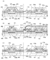
(実施の形態1)
図1(A)に駆動回路に用いる第1の薄膜トランジスタ480と、画素部に用いる第2の薄膜トランジスタ170とを同一基板上に設ける例を示す。なお、図1(A)は表示装置の断面図の一例である。
(Embodiment 1)
FIG. 1A illustrates an example in which a first
画素部と駆動回路は、同一基板上に形成し、画素部においては、マトリクス状に配置したエンハンスメント型トランジスタである第2の薄膜トランジスタ170を用いて画素電極110への電圧印加のオンオフを切り替える。この画素部に配置する第2の薄膜トランジスタ170は、酸化物半導体層103を用いており、第2の薄膜トランジスタの電気特性は、ゲート電圧±20Vにおいて、オンオフ比が109以上であるため表示のコントラストを向上させることができ、さらにリーク電流が少ないため低消費電力駆動を実現することができる。オンオフ比とは、オフ電流とオン電流の比率(ION/IOFF)であり、大きいほどスイッチング特性に優れていると言え、表示のコントラスト向上に寄与する。なお、オン電流とは、トランジスタがオン状態のときに、ソース電極とドレイン電極の間に流れる電流をいう。また、オフ電流とは、トランジスタがオフ状態のときに、ソース電極とドレイン電極の間に流れる電流をいう。例えば、n型のトランジスタの場合には、ゲート電圧がトランジスタのしきい値電圧よりも低いときにソース電極とドレイン電極との間に流れる電流である。このように、高コントラスト、及び低消費電力駆動を実現するためには、画素部にエンハンスメント型トランジスタを用いることが好ましい。
The pixel portion and the driver circuit are formed over the same substrate. In the pixel portion, voltage application to the
駆動回路においては、酸化物半導体層405の下方に第1のゲート電極401と、酸化物半導体層405の上方に第2のゲート電極470とを有する薄膜トランジスタ430を少なくとも一つ用いる。この第2のゲート電極470はバックゲート電極とも呼べる。バックゲート電極を形成することによって、薄膜トランジスタの信頼性を調べるためのバイアス−熱ストレス試験(以下、BT試験という)において、BT試験前後における薄膜トランジスタのしきい値電圧の変化量を低減することができる。
In the driver circuit, at least one
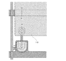
この薄膜トランジスタ430の構造を、図1(A)を用いて説明する。絶縁表面を有する基板400上に設けられた第1のゲート電極401は、第1のゲート絶縁層403に覆われ、第1のゲート電極401と重なる第1のゲート絶縁層403上には、n+層408a及びn+層408bとが設けられる。また、n+層408a及びn+層408b上には、第1配線409または第2配線410が設けられる。ソース電極またはドレイン電極として機能する第1配線409または第2配線410上には、n+層406a及びn+層406bとが設けられる。また、n+層406a及びn+層406b上には、酸化物半導体層405を有する。この酸化物半導体層405を覆う第2のゲート絶縁層412を有する。また、第2のゲート絶縁層412上に第2のゲート電極470を有する。
A structure of the
なお、n+層408a及びn+層408bは、その側面の少なくとも一部が酸化物半導体層405に接している。また、n+層406a及びn+層406bは、その上面の少なくとも一部及びその側面の少なくとも一部が酸化物半導体層405に接している。また、第1配線409及び第2配線410の上下にn+層がそれぞれ設けられているため、第1配線409及び第2配線410の側面と、酸化物半導体層405とが接する面積を縮小することができる。
Incidentally, the n +
n+層は、酸化物半導体層と比較して低抵抗な酸化物半導体層であり、ソース領域又はドレイン領域として機能する。なお、第1配線409がソース電極層として機能し、第2配線410がドレイン電極層として機能する場合、n+層408a及びn+層406aが第1及び第2のソース領域として機能し、n+層408b及びn+層406bが第1及び第2のドレイン領域として機能する。薄膜トランジスタに、複数のソース領域、複数のドレイン領域を設けることで、ソース領域またはドレイン領域が単数の場合よりもさらにトランジスタのオン電流を大きくすることができる。
The n + layer is an oxide semiconductor layer having a lower resistance than the oxide semiconductor layer and functions as a source region or a drain region. Note that when the
また、第1のゲート電極401と第2のゲート電極470とを電気的に接続して同電位としてもよい。同電位とすると、酸化物半導体層の上下からゲート電圧を印加することができるため、オン状態において流れる電流を大きくすることができる。
Alternatively, the
また、しきい値電圧をマイナスにシフトするための制御信号線を第1のゲート電極401、或いは第2のゲート電極470のいずれか一方と電気的に接続することによってデプレッション型のTFTとすることができる。
Further, a depletion type TFT is formed by electrically connecting a control signal line for shifting the threshold voltage to minus with either the
また、しきい値電圧をプラスにシフトするための制御信号線を第1のゲート電極401、或いは第2のゲート電極470のいずれか一方と電気的に接続することによってエンハンスメント型のTFTとすることができる。
Further, an enhancement type TFT is formed by electrically connecting a control signal line for shifting the threshold voltage to plus with either the
また、駆動回路に用いる2つの薄膜トランジスタの組み合わせは特に限定されず、1つのゲート電極を有する薄膜トランジスタをデプレッション型TFTとして用い、2つのゲート電極を有する薄膜トランジスタをエンハンスメント型TFTとして用いてもよい。その場合には、画素部の薄膜トランジスタとして、ゲート電極を酸化物半導体層の上下にそれぞれ有する構造とする。 A combination of two thin film transistors used for the driver circuit is not particularly limited, and a thin film transistor having one gate electrode may be used as a depletion type TFT, and a thin film transistor having two gate electrodes may be used as an enhancement type TFT. In that case, the thin film transistor in the pixel portion has a structure in which gate electrodes are provided above and below the oxide semiconductor layer.
また、画素部の薄膜トランジスタとして、ゲート電極を酸化物半導体層の上下にそれぞれ有する構造とし、駆動回路のエンハンスメント型TFTとして、ゲート電極を酸化物半導体層の上下にそれぞれ有する構造とし、駆動回路のデプレッション型TFTとしてゲート電極を酸化物半導体層の上下にそれぞれ有する構造としてもよい。その場合には、しきい値電圧を制御するための制御信号線を上下どちらか一方のゲート電極に電気的に接続させ、その接続したゲート電極がしきい値を制御する構成とする。 In addition, the thin film transistor in the pixel portion has a structure in which the gate electrode is provided above and below the oxide semiconductor layer, and the enhancement type TFT in the driver circuit has a structure in which the gate electrode is provided above and below the oxide semiconductor layer. The type TFT may have a structure having gate electrodes above and below the oxide semiconductor layer. In that case, a control signal line for controlling the threshold voltage is electrically connected to either the upper or lower gate electrode, and the connected gate electrode controls the threshold value.
なお、図1(A)においては、第2のゲート電極470は、画素部の画素電極110と同じ材料、例えば透過型の液晶表示装置であれば、透明導電膜を用いて工程数を低減しているが、特に限定されない。また、第2のゲート電極470の幅は、第1のゲート電極401の幅よりも広く、さらに酸化物半導体層の幅よりも広い例を示しているが特に限定されない。
Note that in FIG. 1A, the
第2のゲート電極の材料及び幅が図1(A)と異なる例を図1(B)に示す。また、図1(B)は有機発光素子或いは無機発光素子と接続する第2の薄膜トランジスタ170を画素部に有する表示装置の例である。
FIG. 1B shows an example in which the material and width of the second gate electrode are different from those in FIG. FIG. 1B illustrates an example of a display device including a second
図1(B)においては、薄膜トランジスタ432の第2のゲート電極として機能する電極471の材料は金属材料(アルミニウム(Al)や銅(Cu)、チタン(Ti)、タンタル(Ta)、タングステン(W)、モリブデン(Mo)、クロム(Cr)、ネオジム(Nd)、スカンジウム(Sc)から選ばれた元素、または上述した元素を成分とする合金)を用い、断面における電極471の幅は図1(A)の第2のゲート電極470よりも狭い。また、電極471の幅は酸化物半導体層405の幅よりも狭い。幅を狭くすることによって、第2のゲート電極471が、第1配線409、及び第2配線410と第2のゲート絶縁層412を介して重なる面積を低減することができ、寄生容量を小さくすることができる。
In FIG. 1B, the material of the
発光素子は、少なくとも第1の電極472と発光層475と第2の電極474とを有する。図1(B)においては、電極471は、画素部の第1の電極472と同じ材料、例えば、アルミニウムなどを用いて工程数を低減しているが、特に限定されない。また、図1(B)において絶縁層473は、隣り合う画素の第1の電極との絶縁を図るための隔壁として機能する。
The light-emitting element includes at least a first electrode 472, a light-emitting
また、第2のゲート電極の材料及び幅が図1(A)と異なる例を図1(C)に示す。図1(C)においては、薄膜トランジスタ433の第2のゲート電極として機能する電極476の材料は金属材料(アルミニウム(Al)や銅(Cu)、チタン(Ti)、タンタル(Ta)、タングステン(W)、モリブデン(Mo)、クロム(Cr)、ネオジム(Nd)、スカンジウム(Sc)から選ばれた元素、または上述した元素を成分とする合金)を用い、断面における第2のゲート電極の幅は図1(B)よりも狭い。図1(B)よりもさらに幅を狭くすることによって第1配線409、及び第2配線410と第2のゲート絶縁層412を介して重ならないようにすることができ、さらに寄生容量を小さくすることができる。図1(C)に示す電極476の幅は、第1配線409と第2配線410の間隔よりも狭い。このように狭い幅の電極476を形成する場合には、ウェットエッチングなどを用いてレジストマスク端部よりも内側に電極476の両端が位置する工程とすることが好ましい。ただし、図1(C)においては画素電極110と異なる金属材料を用いるため、電極476の形成のためのフォトリソグラフィー工程が1回増加し、マスク数も1枚追加することとなる。
FIG. 1C illustrates an example in which the material and width of the second gate electrode are different from those in FIG. In FIG. 1C, the material of the
液晶表示装置や発光表示装置や電子ペーパに用いるゲート線駆動回路またはソース線駆動回路などの周辺回路、または画素部に対して、上下を2つのゲート電極に挟まれた酸化物半導体を用いた薄膜トランジスタを用い、高速駆動や、低消費電力化を図ることができる。また、工程数を大幅に増加させることなく、同一基板上に画素部と駆動回路との両方を設けることができる。同一基板上に、画素部以外の様々な回路を設けることにより、表示装置の製造コストを低減することができる。 A thin film transistor using an oxide semiconductor sandwiched between two gate electrodes on the top and bottom of a peripheral circuit such as a gate line driver circuit or a source line driver circuit used for a liquid crystal display device, a light emitting display device, or electronic paper, or a pixel portion Can be used for high-speed driving and low power consumption. In addition, both the pixel portion and the driver circuit can be provided over the same substrate without significantly increasing the number of steps. By providing various circuits other than the pixel portion over the same substrate, the manufacturing cost of the display device can be reduced.
また、ソース電極又はドレイン電極の上下に、ソース領域またはドレイン領域を設けることにより、金属層であるソース電極またはドレイン電極と、酸化物半導体層との間を良好な接合としてショットキー接合に比べて熱的にも安定動作を有せしめる。また、チャネルのキャリアを供給する(ソース側)、またはチャネルのキャリアを安定して吸収する(ドレイン側)、またはソース電極(またはドレイン電極)との界面に抵抗成分が作られるのを抑制するためにもソース領域またはドレイン領域を設けることは重要である。また、低抵抗な酸化物半導体層(n+層)を設けることで、高いドレイン電圧でも良好な移動度を保持することができる。 In addition, by providing a source region or a drain region above and below a source electrode or a drain electrode, the source electrode or the drain electrode that is a metal layer and the oxide semiconductor layer can be favorably bonded as compared with a Schottky junction. Thermally stable operation. In addition, in order to suppress supply of channel carriers (source side), stable absorption of channel carriers (drain side), or creation of a resistance component at the interface with the source electrode (or drain electrode) In addition, it is important to provide a source region or a drain region. Further, by providing the low-resistance oxide semiconductor layer (n + layer), favorable mobility can be maintained even at a high drain voltage.
(実施の形態2)
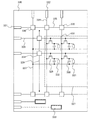
実施の形態1では駆動回路の薄膜トランジスタとして一つの薄膜トランジスタを説明したが、ここでは、2つのnチャネル型の薄膜トランジスタを用いて駆動回路のインバータ回路を構成する例を基に以下に説明する。図2(A)に示す薄膜トランジスタは、実施の形態1の図1(A)に示した薄膜トランジスタ430と同一であるため、同じ部分には同じ符号を用いて説明する。
(Embodiment 2)
In
画素部を駆動するための駆動回路は、インバータ回路、容量、抵抗などを用いて構成する。2つのnチャネル型TFTを組み合わせてインバータ回路を形成する場合、エンハンスメント型トランジスタとデプレッション型トランジスタとを組み合わせて形成する場合(以下、EDMOS回路という)と、エンハンスメント型TFT同士で形成する場合(以下、EEMOS回路という)がある。 A driver circuit for driving the pixel portion is formed using an inverter circuit, a capacitor, a resistor, and the like. When an inverter circuit is formed by combining two n-channel TFTs, an enhancement type transistor and a depletion type transistor are combined (hereinafter referred to as an EDMOS circuit), or an enhancement type TFT (hereinafter referred to as an enhancement type TFT). EEMOS circuit).
駆動回路のインバータ回路の断面構造を図2(A)に示す。なお、図2に示す薄膜トランジスタ430、第2の薄膜トランジスタ431は、ボトムゲート型薄膜トランジスタであり、半導体層下配線が設けられている薄膜トランジスタの例である。
A cross-sectional structure of the inverter circuit of the driver circuit is shown in FIG. Note that each of the
図2(A)において、基板400上に第1のゲート電極401及びゲート電極402を設ける。第1のゲート電極401及びゲート電極402の材料は、モリブデン、チタン、クロム、タンタル、タングステン、アルミニウム、銅、ネオジム、スカンジウム等の金属材料又はこれらを主成分とする合金材料を用いて、単層で又は積層して形成することができる。
In FIG. 2A, a
例えば、第1のゲート電極401及びゲート電極402の2層の積層構造としては、アルミニウム層上にモリブデン層が積層された二層の積層構造、または銅層上にモリブデン層を積層した二層構造、または銅層上に窒化チタン層若しくは窒化タンタル層を積層した二層構造、窒化チタン層とモリブデン層とを積層した二層構造とすることが好ましい。3層の積層構造としては、タングステン層または窒化タングステン層と、アルミニウムとシリコンの合金またはアルミニウムとチタンの合金と、窒化チタン層またはチタン層とを積層した積層とすることが好ましい。
For example, as a two-layer structure of the
また、第1のゲート電極401及びゲート電極402を覆う第1のゲート絶縁層403上方には、第1配線409、第2配線410、第3配線411を設ける。また、第1のゲート絶縁層403と第1配線409、第1のゲート絶縁層403と第2配線410、第1のゲート絶縁層403と第3配線411との間には、それぞれn+層420、421、422を設ける。第2の配線410は、第1のゲート絶縁層403に形成されたコンタクトホール404を介してゲート電極402と接続する。
In addition, a
第1配線409、及び第2配線410の上方には、酸化物半導体層405を設ける。また、第1配線409と酸化物半導体層405、及び第2配線410と酸化物半導体層405との間には、n+層423、424がそれぞれ設けられる。また、第2配線410、及び第3配線411の上方には第2の酸化物半導体層407を設ける。また、第2配線410と酸化物半導体層407、及び第3配線411と酸化物半導体層407との間には、n+層425、426がそれぞれ設けられる。
An
なお、n+層420乃至426は、酸化物半導体層405や酸化物半導体層407に比べて低抵抗な酸化物半導体層であり、ソース領域またはドレイン領域として機能する。配線と酸化物半導体層との間にn+層を有する構成とすることで、ショットキー接合と比べて熱的にも安定動作を有せしめる。
Note that the n + layers 420 to 426 are oxide semiconductor layers having lower resistance than the
薄膜トランジスタ430は、第1のゲート電極401と、第1のゲート絶縁層403を介して第1のゲート電極401と重なる酸化物半導体層405とを有し、第1配線409は、負の電圧VDLが印加される電源線(負電源線)である。この電源線は、接地電位の電源線(接地電源線)としてもよい。
The
また、第2の薄膜トランジスタ431は、ゲート電極402と、第1のゲート絶縁層403を介してゲート電極402と重なる第2の酸化物半導体層407とを有し、第3配線411は、正の電圧VDHが印加される電源線(正電源線)である。
The second
また、駆動回路のインバータ回路の上面図を図2(C)に示す。図2(C)において、鎖線Z1−Z2で切断した断面が図2(A)に相当する。 A top view of the inverter circuit of the driver circuit is shown in FIG. In FIG. 2C, a cross section taken along the chain line Z1-Z2 corresponds to FIG.
また、EDMOS回路の等価回路を図2(B)に示す。図2(A)に示す回路接続は、図2(B)に相当し、薄膜トランジスタ430をエンハンスメント型のnチャネル型トランジスタとし、第2の薄膜トランジスタ431をデプレッション型のnチャネル型トランジスタとする例である。
An equivalent circuit of the EDMOS circuit is shown in FIG. The circuit connection illustrated in FIG. 2A corresponds to FIG. 2B and is an example in which the
薄膜トランジスタ430をエンハンスメント型のnチャネル型トランジスタとするため、本実施の形態では、酸化物半導体層405上に第2のゲート絶縁層412と、該第2のゲート絶縁層412上に第2のゲート電極470を設け、第2のゲート電極470に印加する電圧によって薄膜トランジスタ430のしきい値制御を行う。
In order to make the
また、第2のゲート絶縁層412は、第2の酸化物半導体層407を覆う保護層としても機能する。
The second
なお、図2(A)及び図2(C)では、第2の配線410は、第1のゲート絶縁層403に形成されたコンタクトホール404を介してゲート電極402と直接接続する例を示したが、特に限定されず、接続電極を別途設けて第2の配線410とゲート電極402とを電気的に接続させてもよい。
2A and 2C illustrate an example in which the
また、本実施の形態は、実施の形態1と自由に組み合わせることができる。
Further, this embodiment mode can be freely combined with
(実施の形態3)
本実施の形態では、表示装置について、ブロック図等を参照して説明する。
(Embodiment 3)
In this embodiment, a display device is described with reference to block diagrams and the like.
図3(A)は、アクティブマトリクス型液晶表示装置のブロック図の一例を示す。図3(A)に示す液晶表示装置は、基板300上に表示素子を備えた画素を複数有する画素部301と、各画素のゲート電極に接続された走査線を制御する走査線駆動回路302と、選択された画素へのビデオ信号の入力を制御する信号線駆動回路303と、を有する。
FIG. 3A illustrates an example of a block diagram of an active matrix liquid crystal display device. A liquid crystal display device illustrated in FIG. 3A includes a pixel portion 301 including a plurality of pixels each provided with a display element over a
図3(B)は、アクティブマトリクス型発光表示装置のブロック図の一例を示す。図3(B)に示す発光表示装置は、基板310上に表示素子を備えた画素を複数有する画素部311と、各画素のゲート電極に接続された走査線を制御する第1の走査線駆動回路312及び第2の走査線駆動回路313と、選択された画素へのビデオ信号の入力を制御する信号線駆動回路314と、を有する。一つの画素にスイッチング用TFT(Thin Film Transistor。以下、TFTという。)と電流制御用TFTの2つを配置する場合、図3(B)に示す発光表示装置では、スイッチング用TFTのゲート電極に接続された第1の走査線に入力される信号を第1の走査線駆動回路312で生成し、電流制御用TFTのゲート電極に接続された第2の走査線に入力される信号を第2の走査線駆動回路313で生成する。ただし、第1の走査線に入力される信号と、第2の走査線に入力される信号とを、一の走査線駆動回路で生成する構成としても良い。また、例えば、スイッチング素子が有するTFTの数によって、スイッチング素子の動作を制御するのに用いられる第1の走査線が、各画素に複数設けられていてもよい。この場合、複数の第1の走査線に入力される信号を、全て1つの走査線駆動回路で生成しても良いし、複数の走査線駆動回路を設けてこれらの各々で生成しても良い。
FIG. 3B illustrates an example of a block diagram of an active matrix light-emitting display device. A light-emitting display device illustrated in FIG. 3B includes a pixel portion 311 including a plurality of pixels each provided with a display element over a
なお、ここでは、走査線駆動回路302、第1の走査線駆動回路312、第2の走査線駆動回路313、及び信号線駆動回路303、314を表示装置に作製する形態を示したが、走査線駆動回路302、第1の走査線駆動回路312、または第2の走査線駆動回路313の一部をIC等の半導体装置で実装してもよい。また、信号線駆動回路303、314の一部をIC等の半導体装置で実装してもよい。 Note that although the scan line driver circuit 302, the first scan line driver circuit 312, the second scan line driver circuit 313, and the signal line driver circuits 303 and 314 are formed in the display device here, scanning is performed. Part of the line driver circuit 302, the first scan line driver circuit 312, or the second scan line driver circuit 313 may be mounted using a semiconductor device such as an IC. Further, part of the signal line driver circuits 303 and 314 may be mounted using a semiconductor device such as an IC.
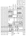
図4は、表示装置を構成する、信号入力端子322、走査線323、信号線324、非線形素子を含む保護回路及び画素部の位置関係を説明する図である。絶縁表面を有する基板320上には走査線323と信号線324が交差して配置され、画素部327が構成されている。なお、画素部327は、図3に示す画素部301と画素部311に相当する。
FIG. 4 is a diagram illustrating the positional relationship between the
画素部301は、信号線駆動回路303から列方向に伸張して配置された複数の信号線S1〜Sm(図示せず。)により信号線駆動回路303と接続され、走査線駆動回路302から行方向に伸張して配置された複数の走査線G1〜Gn(図示せず。)により走査線駆動回路302と接続され、信号線S1〜Sm並びに走査線G1〜Gnに対応してマトリクス状に配置された複数の画素(図示せず。)を有する。そして、各画素は、信号線Sj(信号線S1〜Smのうちいずれか一)、走査線Gi(走査線G1〜Gnのうちいずれか一)と接続される。 The pixel portion 301 is connected to the signal line driver circuit 303 by a plurality of signal lines S1 to Sm (not shown) arranged extending from the signal line driver circuit 303 in the column direction, and is connected to the scanning line driver circuit 302 from the row. A plurality of scanning lines G1 to Gn (not shown) arranged to extend in the direction are connected to the scanning line driving circuit 302 and arranged in a matrix corresponding to the signal lines S1 to Sm and the scanning lines G1 to Gn. A plurality of pixels (not shown). Each pixel is connected to a signal line Sj (any one of the signal lines S1 to Sm) and a scanning line Gi (any one of the scanning lines G1 to Gn).
画素部327は複数の画素328がマトリクス状に配列して構成されている。画素328は、走査線323と信号線324に接続する画素TFT329、保持容量部330、画素電極331を含んで構成されている。
The
ここで示す画素構成において、保持容量部330では、一方の電極と画素TFT329が接続され、他方の電極と容量線332が接続される場合を示している。また、画素電極331は表示素子(液晶素子、発光素子、コントラスト媒体(電子インク)等)を駆動する一方の電極を構成する。これらの表示素子の他方の電極はコモン端子333に接続されている。
In the pixel configuration shown here, in the
保護回路は、画素部327と、信号線入力端子322との間に配設されている。また、走査線駆動回路と、画素部327の間に配設されている。本実施の形態では、複数の保護回路を配設して、走査線323、信号線324及び容量バス線337に静電気等によりサージ電圧が印加され、画素TFT329等が破壊されないように構成されている。そのため、保護回路にはサージ電圧が印加されたときに、コモン配線に電荷を逃がすように構成されている。
The protection circuit is provided between the
本実施の形態では、走査線323側に保護回路334、信号線324側に保護回路335、容量バス線337に保護回路336を配設する例を示している。ただし、保護回路の配設位置はこれに限定されない。また、走査線駆動回路をIC等の半導体装置で実装しない場合は、走査線323側に保護回路334を設けなくとも良い。
In this embodiment, the
これらの回路の各々に実施の形態1または実施の形態2に示したTFTを用いることで、以下の利点がある。
By using the TFT shown in
駆動回路は、論理回路部と、スイッチ部またはバッファ部とに大別される。論理回路部に設けるTFTは閾値電圧を制御することが可能な構成であるとよい。一方で、スイッチ部またはバッファ部に設けるTFTはオン電流が大きいことが好ましい。実施の形態1または実施の形態2に示したTFTを有する駆動回路を設けることで、論理回路部に設けるTFTの閾値電圧の制御が可能となり、スイッチ部またはバッファ部に設けるTFTのオン電流を大きくすることが可能となる。更には、駆動回路が占有する面積を小さくし、狭額縁化にも寄与する。
The drive circuit is roughly divided into a logic circuit part and a switch part or a buffer part. The TFT provided in the logic circuit portion may have a structure capable of controlling the threshold voltage. On the other hand, the TFT provided in the switch portion or the buffer portion preferably has a large on-current. By providing the driver circuit including the TFT described in
また、走査線駆動回路を構成するシフトレジスタ回路について以下に説明する。 A shift register circuit included in the scan line driver circuit is described below.
図5に示すシフトレジスタ回路は、フリップフロップ回路351を複数有し、制御信号線352、制御信号線353、制御信号線354、制御信号線355、制御信号線356、及びリセット線357を有する。
The shift register circuit illustrated in FIG. 5 includes a plurality of flip-
図5のシフトレジスタ回路に示すように、フリップフロップ回路351では、初段の入力端子INに、制御信号線352を介して、スタートパルスSSPが入力され、次段以降の入力端子INに前段のフリップフロップ回路351の出力信号端子SOUTが接続されている。また、N段目(Nは自然数である。)のリセット端子RESは、(N+3)段目のフリップフロップ回路の出力信号端子Soutとリセット線357を介して接続されている。N段目のフリップフロップ回路351のクロック端子CLKには、制御信号線353を介して、第1のクロック信号CLK1が入力されると仮定すると、(N+1)段目のフリップフロップ回路351のクロック端子CLKには、制御信号線354を介して、第2のクロック信号CLK2が入力される。また、(N+2)段目のフリップフロップ回路351のクロック端子CLKには、制御信号線355を介して、第3のクロック信号CLK3が入力される。また、(N+3)段目のフリップフロップ回路351のクロック端子CLKには、制御信号線356を介して、第4のクロック信号CLK4が入力される。そして、(N+4)段目のフリップフロップ回路351のクロック端子CLKには、制御信号線353を介して、第1のクロック信号CLK1が入力される。また、N段目のフリップフロップ回路351は、ゲート出力端子Goutより、N段目のフリップフロップ回路の出力SRoutNを出力する。
As shown in the shift register circuit of FIG. 5, in the flip-
なお、フリップフロップ回路351と、電源及び電源線との接続を図示していないが、各フリップフロップ回路351には電源線を介して電源電位Vdd及び電源電位GNDが供給されている。
Note that although connection between the flip-
なお、本明細書で説明する電源電位は、基準電位を0Vとした場合の、電位差に相当する。そのため、電源電位のことを電源電圧、または電源電圧のことを電源電位と呼ぶこともある。 Note that the power supply potential described in this specification corresponds to a potential difference in a case where the reference potential is 0V. Therefore, the power supply potential may be referred to as a power supply voltage, or the power supply voltage may be referred to as a power supply potential.
なお、本明細書において、AとBとが接続されている、とは、AとBとが直接接続されているものの他、電気的に接続されているものを含むものとする。ここで、AとBとが電気的に接続されているとは、AとBとの間に何らかの電気的作用を有する対象物が存在するとき、対象物を介してAとBとが概略同一ノードとなる場合を表すものとする。具体的には、TFTのようなスイッチング素子を介してAとBとが接続され、該スイッチング素子の導通によって、AとBとが概略同電位となる場合や、抵抗素子を介してAとBとが接続され、該抵抗素子の両端に発生する電位差が、AとBとを含む回路の動作に影響しない程度となっている場合等、回路動作を考えた場合にAとBとを同一ノードとして捉えて差し支えない状態である場合を表す。 Note that in this specification, A and B are connected to each other, including A and B being directly connected, as well as those being electrically connected. Here, A and B are electrically connected when A and B have an object having some electrical action, and A and B are substantially identical through the object. It shall represent the case of becoming a node. Specifically, A and B are connected via a switching element such as a TFT, and when A and B are approximately at the same potential due to conduction of the switching element, or A and B are connected via a resistance element. Are connected to each other and A and B are connected to the same node when considering circuit operation, such as when the potential difference generated at both ends of the resistance element does not affect the operation of the circuit including A and B. It represents the case where it can be understood as.
次に、図6に、図5で示したシフトレジスタ回路が有するフリップフロップ回路351の一形態を示す。図6に示すフリップフロップ回路351は、論理回路部361と、スイッチ部362と、を有する。論理回路部361は、TFT363乃至TFT368を有する。また、スイッチ部362は、TFT369乃至TFT372を有している。なお論理回路部とは、外部より入力される信号に応じて後段の回路であるスイッチ部に出力する信号を切り替えるための回路である。また、スイッチ部とは、外部及び制御回路部から入力される信号に応じてスイッチとなるTFTのオンまたはオフの切り替え、当該TFTのサイズ及び構造に応じた電流を出力するための回路である。
Next, FIG. 6 illustrates one mode of the flip-
フリップフロップ回路351において、入力端子inはTFT364のゲート端子、及びTFT367のゲート端子に接続されている。リセット端子RESは、TFT363のゲート端子に接続されている。クロック端子CLKは、TFT369の第1端子、及びTFT371の第1端子に接続されている。電源電位Vddが供給される電源線は、TFT364の第1端子、並びにTFT366のゲート端子及び第2端子に接続されている。電源電位GNDが供給される電源線は、TFT363の第2端子、TFT365の第2端子、TFT367の第2端子、TFT368の第2端子、TFT370の第2端子、及びTFT372の第2端子に接続されている。また、TFT363の第1端子、TFT364の第2端子、TFT365の第1端子、TFT368のゲート端子、TFT369のゲート端子、及びTFT371のゲート端子は互いに接続されている。また、TFT366の第1端子は、TFT365のゲート端子、TFT367の第1端子、TFT368の第1端子、TFT370のゲート端子、及びTFT372のゲート端子に接続されている。また、ゲート出力端子Goutは、TFT369の第2端子、及びTFT370の第1端子に接続されている。出力信号端子Soutは、TFT371の第2端子、及びTFT372の第1端子に接続されている。
In the flip-
なお、ここでは、TFT363乃至TFT372が、すべてN型TFTである例についての説明を行う。
Here, an example in which the
なお、TFTは、ゲートと、ドレインと、ソースと、を含む少なくとも三つの端子を有する素子であり、ドレイン領域とソース領域の間にチャネル形成領域を有し、ドレイン領域とチャネル形成領域とソース領域とを介して電流を流すことができる。ここで、ソースとドレインは、TFTの構造や動作条件等によって入れ替わることがあるため、いずれがソースであり、いずれがドレインであるかを特定することが困難である。そこで、ソース及びドレインとして機能する領域を、ソースもしくはドレインと呼ばず、例えば、それぞれを第1端子、第2端子と表記する場合もある。また、この場合に、ゲートとして機能する端子については、ゲート端子と表記する。 Note that a TFT is an element having at least three terminals including a gate, a drain, and a source, has a channel formation region between the drain region and the source region, and the drain region, the channel formation region, and the source region. A current can be passed through. Here, since the source and the drain may be interchanged depending on the structure or operating conditions of the TFT, it is difficult to specify which is the source and which is the drain. Therefore, regions functioning as a source and a drain are not referred to as a source or a drain, but may be referred to as a first terminal and a second terminal, for example. In this case, a terminal functioning as a gate is referred to as a gate terminal.
次に、図6に示したフリップフロップ回路351のレイアウト図の一例を図7に示す。
Next, an example of a layout diagram of the flip-
図7のフリップフロップ回路は、電源電位Vddが供給される電源線381、リセット線382、制御信号線353、制御信号線354、制御信号線355、制御信号線356、制御信号線383、電源電位GNDが供給される電源線384、論理回路部361、及びスイッチ部362を有する。論理回路部361は、TFT363乃至TFT368を有する。また、スイッチ部362は、TFT369乃至TFT372を有している。また、図7では、ゲート出力端子Goutに接続される配線、出力信号端子Soutに接続される配線についても示している。
The flip-flop circuit in FIG. 7 includes a
図7中では、半導体層385、第1の配線層386、第2の配線層387、第3の配線層388、コンタクトホール389について示している。なお、第1の配線層386は、ゲート電極を形成する層により形成し、第2の配線層387は、TFTのソース電極又はドレイン電極を形成する層により形成し、第3の配線層388は、画素部における画素電極を形成する層により形成すればよい。ただし、これに限定されず、例えば第3の配線層388を、画素電極を形成する層とは別の配線層として形成しても良い。
In FIG. 7, the
なお、図7中の各回路素子間の接続関係は、図6で説明した通りである。なお、図7では、第1のクロック信号が入力されるフリップフロップ回路について示しているため、制御信号線354乃至制御信号線356との接続については図示されていない。
In addition, the connection relation between each circuit element in FIG. 7 is as having demonstrated in FIG. Note that FIG. 7 illustrates the flip-flop circuit to which the first clock signal is input; therefore, connection with the
図7のフリップフロップ回路のレイアウト図において、論理回路部361が有するTFT366またはTFT367のしきい値電圧を制御することで、EDMOS回路373を構成することができる。代表的には、TFT366をデプレッション型とし、TFT367をエンハンスメント型としたEDMOS回路373で構成し、スイッチ部362が有するTFT369乃至TFT372をデュアルゲート型のTFT、またはデプレッション型のTFTとする。なお、図6において、EDMOS回路373におけるTFT366とTFT367は図2に示したEDMOS回路とは、デプレッション型のTFTのゲート電極の接続位置が異なっている。
In the layout diagram of the flip-flop circuit in FIG. 7, the EDMOS circuit 373 can be formed by controlling the threshold voltage of the
TFT366またはTFT367をデュアルゲート型のTFTで形成し、バックゲート電極の電位を制御することで、デプレッション型のTFT、或いはエンハンスメント型のTFTとすることができる。
By forming the
図7では、TFT366のしきい値電圧を制御するためのバックゲート電極と同電位の制御信号線390を別途設けて、デプレッション型としている。TFT366はデュアルゲート型のTFTであり、バックゲート電極の電位は、ゲート電極に印加される電源電位Vddが供給される電源線381とは異なる電位である。
In FIG. 7, a
図7においては、TFT369〜372は、デュアルゲート型のTFTであり、バックゲート電極とゲート電極が同電位である例であり、バックゲート電極の電位は、ゲート電極に印加される電源電位Vddが供給される電源線と同じ電位である。
In FIG. 7,
このようにして、表示装置の画素部および駆動回路に配置するTFTを酸化物半導体層を用いたnチャネル型TFTのみで形成することができる。 In this manner, TFTs disposed in the pixel portion and the driver circuit of the display device can be formed using only n-channel TFTs using an oxide semiconductor layer.
また、論理回路部361におけるTFT366は電源電位Vddに応じて電流を流すためのTFTであり、TFT366をデュアルゲート型TFTまたはデプレッション型のTFTとして、流れる電流を大きくすることにより、性能を低下させることなく、TFTの小型化を図ることができる。
In addition, the
また、スイッチ部362を構成するTFTにおいて、TFTを流れる電流量を大きくし、且つオンとオフの切り替えを高速に行うことができるため、性能を低下させることなくTFTが占める面積を縮小することができる。従って、該TFTにより構成される回路が占める面積を縮小することもできる。なお、スイッチ部362におけるTFT369乃至TFT372は、図示するように半導体層385を第1の配線層386及び第3の配線層388で挟むようにレイアウトして、デュアルゲート型TFTを形成すればよい。
Further, in the TFT constituting the
また、図7では、デュアルゲート型TFTが、半導体層385を第1の配線層386と、コンタクトホール389により第1の配線層386に接続されて同電位となった第3の配線層388と、により挟まれて構成される例を示したが、この構成に限定されない。例えば、第3の配線層388に対して、別途制御信号線を設け、第3の配線層388の電位を第1の配線層386から独立して制御する構成としてもよい。
In FIG. 7, the dual-gate TFT includes a
なお、図7に示すフリップフロップ回路のレイアウト図において、TFT363乃至TFT372のチャネル形成領域の形状をU字型(コの字型又は馬蹄型)にしてもよい。また、図7中では、各TFTのサイズを等しくしているが、後段の負荷の大きさに応じて出力信号端子Soutまたはゲート出力端子Goutに接続される各TFTの大きさを適宜変更しても良い。
Note that in the layout diagram of the flip-flop circuit illustrated in FIG. 7, the shape of the channel formation region of the
次に、図8に示すタイミングチャートを用いて、図5に示すシフトレジスタ回路の動作について説明する。図8は、図5に示した制御信号線352乃至制御信号線356にそれぞれ供給されるスタートパルスSSP、第1のクロック信号CLK1乃至第4のクロック信号CLK4、及び1段目乃至5段目のフリップフロップ回路の出力信号端子Soutから出力されるSout1乃至Sout5について示している。なお、図8の説明では、図6及び図7において各素子に付した符号を用いる。
Next, operation of the shift register circuit illustrated in FIG. 5 is described with reference to a timing chart illustrated in FIG. 8 illustrates the start pulse SSP, the first clock signal CLK1 to the fourth clock signal CLK4, and the first to fifth stages supplied to the
なお、図8は、フリップフロップ回路が有するTFTのそれぞれが、N型TFTの場合のタイミングチャートである。また第1のクロック信号CLK1及び第4のクロック信号CLK4は図示するように1/4波長(点線にて区分けした一区間)ずつシフトした構成となっている。 FIG. 8 is a timing chart in the case where each TFT included in the flip-flop circuit is an N-type TFT. The first clock signal CLK1 and the fourth clock signal CLK4 are shifted by a quarter wavelength (one section divided by a dotted line) as shown in the figure.
まず、期間T1において、1段目のフリップフロップ回路には、スタートパルスSSPがHレベルで入力され、論理回路部361はスイッチ部のTFT369及びTFT371をオンし、TFT370及びTFT372をオフにする。このとき、第1のクロック信号CLK1はLレベルであるため、Sout1はLレベルである。
First, in the period T1, the start pulse SSP is input to the first flip-flop circuit at the H level, and the
なお、期間T1において、2段目以降のフリップフロップ回路には、IN端子に信号が入力されないため、動作することなくLレベルを出力している。なお、初期状態では、シフトレジスタ回路の各フリップフロップ回路は、Lレベルを出力するものとして説明を行う。 Note that in the period T1, since no signal is input to the IN terminal of the second and subsequent flip-flop circuits, the L level is output without being operated. In the initial state, each flip-flop circuit of the shift register circuit will be described as outputting L level.
次に、期間T2において、1段目のフリップフロップ回路では、期間T1と同様に、論理回路部361がスイッチ部362の制御を行う。期間T2では、第1のクロック信号CLK1はHレベルとなるため、Sout1はHレベルとなる。また、期間T2では、2段目のフリップフロップ回路には、Sout1がHレベルでIN端子に入力され、論理回路部361がスイッチ部のTFT369及びTFT371をオンし、TFT370及びTFT372をオフする。このとき、第2のクロック信号CLK2はLレベルであるため、Sout2はLレベルである。
Next, in the period T2, in the flip-flop circuit in the first stage, the
なお、期間T2において、3段目以降のフリップフロップ回路には、IN端子に信号が入力されないため、動作することなくLレベルを出力している。 Note that in the period T2, since no signal is input to the IN terminal in the third and subsequent flip-flop circuits, the L level is output without being operated.
次に、期間T3において、1段目のフリップフロップ回路では、期間T2の状態を保持するように論理回路部361がスイッチ部362の制御を行う。そのため、期間T3では、第1のクロック信号CLK1はHレベルであり、Sout1はHレベルとなる。また、期間T3において、2段目のフリップフロップ回路では、期間T2と同様に、論理回路部361がスイッチ部362の制御を行う。期間T3では、第2のクロック信号CLK2はHレベルであるため、Sout2はHレベルである。また、期間T3の3段目のフリップフロップ回路には、Sout2がHレベルでIN端子に入力され、論理回路部361がスイッチ部のTFT369及び371をオンし、TFT370及び372をオフにする。このとき、第3のクロック信号CLK3はLレベルであるため、Sout3はLレベルである。
Next, in the period T3, in the flip-flop circuit in the first stage, the
なお、期間T3において、4段目以降のフリップフロップ回路には、IN端子に信号が入力されないため、動作することなくLレベルを出力している。 Note that in the period T3, no signal is input to the IN terminal of the fourth and subsequent flip-flop circuits, and thus the L level is output without operation.
次に、期間T4において、1段目のフリップフロップ回路では、期間T3の状態を保持するように論理回路部361がスイッチ部362の制御を行う。そのため、期間T4において、第1のクロック信号CLK1はLレベルであり、Sout1はLレベルとなる。また、期間T4において、2段目のフリップフロップ回路では、期間T3の状態を保持するように論理回路部361がスイッチ部362の制御を行う。そのため、期間T4において、第2のクロック信号CLK2はHレベルであり、Sout2はHレベルとなる。また、期間T4において、3段目のフリップフロップ回路では、期間T3と同様に、論理回路部361がスイッチ部362の制御を行う。期間T4では、第3のクロック信号CLK3はHレベルであるため、Sout3はHレベルである。また、期間T4の4段目のフリップフロップ回路には、Sout3がHレベルでIN端子に入力され、論理回路部361がスイッチ部362のTFT369及びTFT371をオンし、TFT370及びTFT372をオフにする。このとき、第4のクロック信号CLK4はLレベルであるため、Sout4はLレベルである。
Next, in the period T4, in the flip-flop circuit in the first stage, the
なお、期間T4において、5段目以降のフリップフロップ回路には、IN端子に信号が入力されないため、動作することなくLレベルを出力している。 Note that in the period T4, since no signal is input to the IN terminal of the fifth and subsequent flip-flop circuits, the L level is output without operation.
次に、期間T5において、2段目のフリップフロップ回路では、期間T3の状態を保持するように論理回路部361がスイッチ部362の制御を行う。そのため、期間T5において、第2のクロック信号CLK2はLレベルであり、Sout2はLレベルとなる。また、期間T5において、3段目のフリップフロップ回路では、期間T4の状態を保持するように論理回路部361がスイッチ部362の制御を行う。そのため、期間T5において、第3のクロック信号CLK3はHレベルであり、Sout3はHレベルとなる。また、期間T5において4段目のフリップフロップ回路には、期間T4と同様に、論理回路部361がスイッチ部362の制御を行う。期間T5では、第4のクロック信号CLK4はHレベルであるため、Sout4はHレベルである。また、5段目以降のフリップフロップ回路は、1段目乃至4段目のフリップフロップ回路と同様の配線関係であり、入力される信号のタイミングも同様であるため、説明は省略する。
Next, in the period T5, in the flip-flop circuit at the second stage, the
図5のシフトレジスタ回路で示したように、Sout4は1段目のフリップフロップ回路のリセット信号を兼ねる。期間T5では、Sout4がHレベルとなり、この信号が1段目のフリップフロップ回路のリセット端子RESに入力される。リセット信号が入力されることにより、スイッチ部362のTFT369及びTFT371をオフし、TFT370及びTFT372をオンする。そして、1段目のフリップフロップ回路のSout1は、次のスタートパルスSSPが入力されるまで、Lレベルを出力することになる。
As shown in the shift register circuit of FIG. 5, Sout4 also serves as a reset signal for the first-stage flip-flop circuit. In the period T5, Sout4 becomes H level, and this signal is input to the reset terminal RES of the first-stage flip-flop circuit. When the reset signal is input, the
以上説明した動作により、2段目以降のフリップフロップ回路でも、後段のフリップフロップ回路から出力されるリセット信号に基づいて論理回路部のリセットが行われ、Sout1乃至Sout5に示すように、クロック信号の1/4波長分シフトした波形の信号を出力するシフトレジスタ回路とすることができる。 With the operation described above, the flip-flop circuits in the second and subsequent stages also reset the logic circuit portion based on the reset signal output from the flip-flop circuit in the subsequent stage, and as shown in Sout1 to Sout5, A shift register circuit that outputs a signal having a waveform shifted by ¼ wavelength can be obtained.
また、フリップフロップ回路として、論理回路部にエンハンスメント型とデプレッション型を組み合わせたEDMOSのTFT、スイッチ部にデュアルゲート型のTFTを具備する構成とすることにより、論理回路部361を構成するTFTを流れる電流量を大きくすることができ、性能を低下させることなく、TFTが占める面積、更には該TFTにより構成される回路が占める面積を縮小することができる。また、スイッチ部362を構成するTFTにおいては、TFTを流れる電流量を大きくし、オンとオフの切り替えを高速に行うことができるため、性能を低下させることなくTFTが占める面積、更には該TFTにより構成される回路が占める面積を縮小することができる。従って、表示装置の狭額縁化、小型化、高性能化を図ることができる。
In addition, the flip-flop circuit includes an EDMOS TFT that combines an enhancement type and a depletion type in the logic circuit portion, and a dual gate TFT in the switch portion, so that the TFT constituting the
また、図3に示す信号線駆動回路に、ラッチ回路、レベルシフタ回路等を設けることができる。信号線駆動回路から画素部に信号を送る最終段にバッファ部を設け、増幅した信号を信号線駆動回路から画素部に送る。このため、バッファ部に、オン電流が大きいTFT、代表的にはデュアルゲート型のTFTまたはデプレッション型のTFTを設けることで、TFTの面積を縮小することが可能であり、信号線駆動回路が占める面積を縮小することができる。従って、表示装置の狭額縁化、小型化、高性能化を図ることができる。なお、信号線駆動回路の一部であるシフトレジスタは、高速な動作を必要とされるため、IC等を用いて表示装置に実装することが好ましい。 In addition, a latch circuit, a level shifter circuit, or the like can be provided in the signal line driver circuit illustrated in FIG. A buffer unit is provided at the final stage for transmitting a signal from the signal line driver circuit to the pixel unit, and the amplified signal is transmitted from the signal line driver circuit to the pixel unit. Therefore, by providing a TFT having a large on-current, typically a dual gate TFT or a depletion TFT, in the buffer portion, the area of the TFT can be reduced, and the signal line driver circuit occupies it. The area can be reduced. Accordingly, it is possible to reduce the frame size, size, and performance of the display device. Note that a shift register which is part of the signal line driver circuit is required to operate at high speed, and thus is preferably mounted on a display device using an IC or the like.
また、本実施の形態は、実施の形態1または実施の形態2と自由に組み合わせることができる。
Further, this embodiment can be freely combined with
(実施の形態4)
本実施の形態では、実施の形態1に示した第2の薄膜トランジスタ170を含む表示装置の作製工程について、図9乃至図16を用いて説明する。
(Embodiment 4)
In this embodiment, a manufacturing process of a display device including the second
図9(A)において、透光性を有する基板100にはコーニング社の7059ガラスや1737ガラスなどに代表されるバリウムホウケイ酸ガラスやアルミノホウケイ酸ガラスなどのガラス基板を用いることができる。
In FIG. 9A, a glass substrate such as barium borosilicate glass or alumino borosilicate glass typified by Corning 7059 glass or 1737 glass can be used for the light-transmitting
次いで、導電層を基板100全面に形成した後、第1のフォトリソグラフィー工程を行い、レジストマスクを形成し、エッチングにより不要な部分を除去して配線及び電極(ゲート電極101を含むゲート配線、容量配線108、及び第1の端子121)を形成する。このとき少なくともゲート電極101の端部にテーパー形状が形成されるようにエッチングする。この段階での断面図を図9(A)に示した。なお、この段階での上面図が図11に相当する。なお、レジストマスクの形成にスピンコート法を用いる場合、レジスト膜の均一性の向上のため、大量のレジスト材料や、大量の現像液が使用され、余分な材料の消費量が多い。特に基板が大型化すると、スピンコート法を用いる成膜方法では、大型の基板を回転させる機構が大規模となる点、材料液のロスおよび廃液量が多い点で大量生産上、不利である。また、矩形の基板をスピンコートさせると回転軸を中心とする円形のムラが塗布膜に生じやすい。そこで、インクジェット法などの液滴吐出法やスクリーン印刷法などを用いて選択的にレジスト材料膜を形成し、露光を行ってレジストマスクを形成することが好ましい。選択的にレジスト材料膜を形成することによって、レジスト材料の使用量の削減が図れるため大幅なコストダウンが実現でき、1000mm×1200mm、1100mm×1250mm、1150mm×1300mmのような大面積基板にも対応できる。
Next, after a conductive layer is formed over the entire surface of the
ゲート電極101を含むゲート配線と容量配線108、端子部の第1の端子121は、アルミニウム(Al)や銅(Cu)などの低抵抗導電性材料で形成することが望ましいが、Al単体では耐熱性が劣り、また腐蝕しやすい等の問題点があるので耐熱性導電性材料と組み合わせて形成する。耐熱性導電性材料としては、チタン(Ti)、タンタル(Ta)、タングステン(W)、モリブデン(Mo)、クロム(Cr)、ネオジム(Nd)、スカンジウム(Sc)から選ばれた元素、または上述した元素を成分とする合金か、上述した元素を組み合わせた合金膜、または上述した元素を成分とする窒化物で形成する。
The gate wiring including the
次いで、ゲート電極101上にゲート絶縁層102を全面に成膜する。ゲート絶縁層102はスパッタ法などを用い、膜厚を50〜400nmとする。薄膜トランジスタの歩留まりを優先する場合には、ゲート絶縁層102の膜厚は厚いほうが好ましい。
Next, a
例えば、ゲート絶縁層102としてスパッタ法により酸化シリコン膜を用い、100nmの厚さで形成する。勿論、ゲート絶縁層102はこのような酸化シリコン膜に限定されるものでなく、酸化窒化シリコン膜、窒化シリコン膜、酸化アルミニウム膜、窒化アルミニウム膜、酸化窒化アルミニウム膜、酸化タンタル膜などの他の絶縁膜を用い、これらの材料から成る単層または積層構造として形成しても良い。また、ゲート絶縁層102として酸化窒化シリコン膜、または窒化シリコン膜などを用いる場合、ガラス基板からの不純物、例えばナトリウムなどが拡散し、後に形成する酸化物半導体に侵入することをブロックすることができる。
For example, the
次いで、第2のフォトリソグラフィー工程を行い、レジストマスクを形成し、エッチングにより不要な部分を除去してゲート電極と同じ材料の配線や電極に達するコンタクトホールを形成する。このコンタクトホールは後に形成する導電膜と直接接続するために設ける。例えば、駆動回路部において、ゲート電極とソース電極或いはドレイン電極と直接接する薄膜トランジスタや、端子部のゲート配線と電気的に接続する端子を形成する場合にコンタクトホールを形成する。なお、ここでは第2のフォトリソグラフィー工程を行って、後に形成する導電膜と直接接続するためのコンタクトホールを形成する例を示したが、特に限定されず、後で画素電極との接続のためのコンタクトホールと同じ工程でゲート電極層に達するコンタクトホールを形成し、画素電極と同じ材料で電気的な接続を行ってもよい。画素電極と同じ材料で電気的な接続を行う場合にはマスク数を1枚削減することができる。 Next, a second photolithography step is performed, a resist mask is formed, unnecessary portions are removed by etching, and contact holes reaching the wirings and electrodes of the same material as the gate electrode are formed. This contact hole is provided for direct connection to a conductive film to be formed later. For example, a contact hole is formed when a thin film transistor in direct contact with a gate electrode and a source electrode or a drain electrode or a terminal electrically connected to a gate wiring in a terminal portion is formed in a driver circuit portion. Note that here, an example is shown in which the second photolithography step is performed to form a contact hole for direct connection with a conductive film to be formed later; however, there is no particular limitation; for connection with a pixel electrode later A contact hole that reaches the gate electrode layer may be formed in the same process as the contact hole, and electrical connection may be made using the same material as the pixel electrode. When electrical connection is made using the same material as the pixel electrode, the number of masks can be reduced by one.
次に、ゲート絶縁層102上に、第1のn+膜(本実施の形態では、In−Ga−Zn−O系非単結晶膜)をスパッタ法で成膜する。n+膜は、In2O3:Ga2O3:ZnO=1:1:1としたターゲットを用い、成膜条件は、圧力を0.4Paとし、電力を500Wとし、成膜温度を室温とし、アルゴンガス流量40sccmを導入してスパッタ成膜を行う。In2O3:Ga2O3:ZnO=1:1:1としたターゲットを意図的に用いているにも関わらず、成膜直後で大きさ1nm〜10nmの結晶粒を含むIn−Ga−Zn−O系非単結晶膜が形成されることがある。なお、ターゲットの成分比、成膜圧力(0.1Pa〜2.0Pa)、電力(250W〜3000W:8インチφ)、温度(室温〜100℃)、反応性スパッタの成膜条件などを適宜調節することで結晶粒の有無や、結晶粒の密度や、直径サイズは、1nm〜10nmの範囲で調節されうると言える。第1のn+膜の膜厚は、5nm〜20nmとする。勿論、膜中に結晶粒が含まれる場合、含まれる結晶粒のサイズが膜厚を超える大きさとならない。本実施の形態では第1のn+膜の膜厚は、5nmとする。
Next, a first n + film (in this embodiment, an In—Ga—Zn—O-based non-single-crystal film) is formed over the
次に、第1のn+膜上に金属材料からなる導電膜をスパッタ法や真空蒸着法で形成する。ここではTi膜、Ndを含むアルミニウム膜、Ti膜の3層構造とする。導電膜の材料としては、Al、Cr、Ta、Ti、Mo、Wから選ばれた元素、または上述した元素を成分とする合金か、上述した元素を組み合わせた合金膜等が挙げられる。また、導電膜は、2層構造としてもよく、アルミニウム膜上にチタン膜を積層してもよい。また、導電膜は、シリコンを含むアルミニウム膜の単層構造や、チタン膜の単層構造としてもよい。 Next, a conductive film made of a metal material is formed over the first n + film by a sputtering method or a vacuum evaporation method. Here, a three-layer structure of a Ti film, an aluminum film containing Nd, and a Ti film is employed. Examples of the material for the conductive film include an element selected from Al, Cr, Ta, Ti, Mo, and W, an alloy containing the above-described element as a component, or an alloy film combining the above-described elements. The conductive film may have a two-layer structure, and a titanium film may be stacked over the aluminum film. The conductive film may have a single-layer structure of an aluminum film containing silicon or a single-layer structure of a titanium film.
次に、導電膜上に第2のn+膜(本実施の形態では、In−Ga−Zn−O系非単結晶膜)をスパッタ法で成膜する。この第2のn+膜は、第1のn+膜と同じ成膜条件を用いて形成することができる。第2のn+膜は、成膜直後で大きさ1nm〜10nmの結晶粒を含む場合のあるIn−Ga−Zn−O系非単結晶膜を用いる。第2のn+膜の膜厚は、5nm〜20nmとする。本実施の形態では第2のn+膜の膜厚は、5nmとする。 Next, a second n + film (in this embodiment, an In—Ga—Zn—O-based non-single-crystal film) is formed over the conductive film by a sputtering method. The second n + film can be formed using the same film formation conditions as the first n + film. As the second n + film, an In—Ga—Zn—O-based non-single-crystal film that may contain crystal grains with a size of 1 nm to 10 nm immediately after the film formation is used. The film thickness of the second n + film is 5 nm to 20 nm. In this embodiment mode, the thickness of the second n + film is 5 nm.
ゲート絶縁層102、第1のn+膜、導電膜、及び第2のn+膜は、スパッタ法で、チャンバーに導入するガスまたは設置するターゲットを適宣切り替えることにより大気に触れることなく連続成膜することができる。大気に触れることなく連続成膜すると、不純物の混入を防止することができる。大気に触れることなく連続成膜する場合、マルチチャンバー方式の製造装置を用いることが好ましい。
The
なお、本実施の形態において導電膜は上下をIn−Ga−Zn−O系非単結晶膜よりなる第1及び第2のn+膜で挟まれて形成されている。このときIn−Ga−Zn−O系非単結晶膜は、バリアメタルとして機能することが可能なため、導電膜をアルミニウム膜の単層としても良い。導電膜をアルミニウム膜の単膜とすることで、スパッタ法で、チャンバーに設置するターゲットを1種類とすることができ、コストの削減を図ることができる。 Note that in this embodiment, the conductive film is formed so that the upper and lower sides are sandwiched between first and second n + films formed of an In—Ga—Zn—O-based non-single-crystal film. At this time, since the In—Ga—Zn—O-based non-single-crystal film can function as a barrier metal, the conductive film may be a single layer of an aluminum film. When the conductive film is a single film of an aluminum film, a single target can be set in the chamber by a sputtering method, and cost can be reduced.
次に、第3のフォトリソグラフィー工程を行い、レジストマスクを形成し、エッチングにより不要な部分を除去して第1のソース領域106a及び第1のドレイン領域106b、ソース電極層105a及びドレイン電極層105b、第2のn+膜よりなるn+層141a、141bを形成する。この際のエッチング方法としてウェットエッチングまたはドライエッチングを用いる。ここでは、ITO07N(関東化学社製)を用いたウェットエッチングにより、n+層141a、141bを形成した後、Ti膜のエッチャントとしてアンモニア過水(過酸化水素:アンモニア:水=5:2:2)を用い、Ndを含むアルミニウム膜のエッチングには燐酸と酢酸と硝酸を混ぜた溶液を用いてそれぞれエッチングを行う。このウェットエッチングにより、Ti膜とAl−Nd膜とTi膜を順次積層した導電膜をエッチングしてソース電極層105a及びドレイン電極層105bを形成する。その後、同じレジストマスクを用いてITO07N(関東化学社製)を用いたウェットエッチングにより、第1のソース領域106a及び第1のドレイン領域106bを形成する。この段階での断面図を図9(B)に示した。なお、この段階での上面図が図12に相当する。
Next, a third photolithography step is performed, a resist mask is formed, unnecessary portions are removed by etching, and the
端子部において、接続電極120は、ゲート絶縁層に形成されたコンタクトホールを介して端子部の第1の端子121と直接接続される。また、接続電極120上に第2のn+膜よりなるn+層145が残存する。また、接続電極120の下方に存在し、且つ第1の端子121と重なる第1のn+膜よりなるn+層143が残存する。第2の端子122上には、第2のn+膜よりなるn+層144が残存し、第2の端子122の下方には、第1のn+膜よりなるn+層142が残存する。なお、ここでは図示しないが、上述した工程と同じ工程を経て駆動回路の薄膜トランジスタのソース配線或いはドレイン配線とゲート電極が直接接続される。また、容量部においては、容量配線108と重なる第1及び第2のn+膜は除去される。
In the terminal portion, the
次に、レジストマスクを除去した後、表面に付着するゴミなどを除去するためのプラズマ処理を行うことが好ましい。この段階での断面図を図9(C)に示す。ここではアルゴンガスを導入してRF電源によりプラズマを発生させる逆スパッタを行い、露出しているゲート絶縁層にプラズマ処理を行う。 Next, after removing the resist mask, it is preferable to perform plasma treatment for removing dust and the like attached to the surface. A cross-sectional view at this stage is illustrated in FIG. Here, reverse sputtering is performed in which argon gas is introduced and plasma is generated by an RF power source, and plasma treatment is performed on the exposed gate insulating layer.
ソース電極層105a及びドレイン電極層105b上には第2のn+膜であるn+層141a、141bが設けられているため、プラズマダメージが低減される。また、第2のn+膜であるn+層141a、141bが設けられているため、ソース電極層105a及びドレイン電極層105bの酸化による配線抵抗の増大を抑えることができる。
Since n + layers 141a and 141b which are second n + films are provided over the
次いで、プラズマ処理後、酸化物半導体膜を成膜する。プラズマ処理後、大気に曝すことなく酸化物半導体膜を成膜することは、ゲート絶縁層と酸化物半導体膜の界面にゴミなどを付着させない点で有用である。ここでは、直径8インチのIn(インジウム)、Ga(ガリウム)、及びZn(亜鉛)を含む酸化物半導体ターゲット(In2O3:Ga2O3:ZnO=1:1:1)を用いて、基板とターゲットの間との距離を170mm、圧力0.4Pa、直流(DC)電源0.5kW、アルゴン又は酸素雰囲気下で成膜する。なお、パルス直流(DC)電源を用いると、ごみが軽減でき、膜厚分布も均一となるために好ましい。酸化物半導体膜の膜厚は、5nm〜200nmとする。本実施の形態では酸化物半導体膜の膜厚は、100nmとする。 Next, after the plasma treatment, an oxide semiconductor film is formed. After the plasma treatment, forming an oxide semiconductor film without exposure to the air is useful in that dust or the like is not attached to the interface between the gate insulating layer and the oxide semiconductor film. Here, an oxide semiconductor target (In 2 O 3 : Ga 2 O 3 : ZnO = 1: 1: 1) containing In (indium), Ga (gallium), and Zn (zinc) having a diameter of 8 inches is used. The distance between the substrate and the target is 170 mm, the pressure is 0.4 Pa, the direct current (DC) power supply is 0.5 kW, and the film is formed in an argon or oxygen atmosphere. Note that a pulse direct current (DC) power source is preferable because dust can be reduced and the film thickness can be uniform. The thickness of the oxide semiconductor film is 5 nm to 200 nm. In this embodiment, the thickness of the oxide semiconductor film is 100 nm.
次に、第4のフォトリソグラフィー工程を行い、レジストマスクを形成し、エッチングにより不要な部分を除去して酸化物半導体層103を形成する。ここではITO07N(関東化学社製)を用いたウェットエッチングにより、不要な部分を除去して酸化物半導体層103を形成する。なお、第1のn+膜、第2のn+膜、及び酸化物半導体膜は同じエッチャントを用いるため、ここでのエッチングにより第1のn+膜の一部及び第2のn+膜の一部が除去される。酸化物半導体膜で覆われ、残存した第2のn+膜は、それぞれ第2のソース領域146a、及び第2のドレイン領域146bとなる。なお、ここでのエッチングは、ウェットエッチングに限定されずドライエッチングを用いてもよい。その後、レジストマスクを除去する。
Next, a fourth photolithography step is performed to form a resist mask, and unnecessary portions are removed by etching, so that the
また、この第4のフォトリソグラフィー工程において、ソース電極層又はドレイン電極層105a、105bと同じ材料である第2の端子を端子部に残す。なお、第2の端子122はソース配線(ソース電極層又はドレイン電極層105a、105bを含むソース配線)と電気的に接続されている。
In the fourth photolithography step, a second terminal which is the same material as the source or drain
次いで、200℃〜600℃、代表的には300℃〜500℃の熱処理を行うことが好ましい。例えば炉に入れ、窒素雰囲気下または大気雰囲気下で350℃、1時間の熱処理を行う。以上の工程で酸化物半導体層103をチャネル形成領域とする薄膜トランジスタ170が作製できる。この段階での断面図を図10(A)に示した。なお、この段階での上面図が図13に相当する。なお、熱処理を行うタイミングは、酸化物半導体膜の成膜後であれば特に限定されず、例えば保護絶縁膜形成後に行ってもよい。
Next, it is preferable to perform heat treatment at 200 ° C. to 600 ° C., typically 300 ° C. to 500 ° C. For example, it is placed in a furnace and heat treatment is performed at 350 ° C. for 1 hour in a nitrogen atmosphere or an air atmosphere. Through the above process, the
さらに、露出している酸化物半導体層103の表面に、酸素ラジカル処理を行ってもよい。酸素ラジカル処理を行うことにより薄膜トランジスタをノーマリーオフとすることができる。また、ラジカル処理を行うことにより、酸化物半導体層103のエッチングによるダメージを回復することができる。ラジカル処理はO2、N2O、好ましくは酸素を含むN2、He、Ar雰囲気下で行うことが好ましい。また、上記雰囲気にCl2、CF4を加えた雰囲気下で行ってもよい。なお、ラジカル処理は、無バイアスで行うことが好ましい。
Further, oxygen radical treatment may be performed on the exposed surface of the
次いで、第2の薄膜トランジスタ170を覆う保護絶縁層107を形成する。保護絶縁層107はスパッタ法などを用いて得られる窒化シリコン膜、酸化シリコン膜、酸化窒化シリコン膜、酸化アルミニウム膜、窒化アルミニウム膜、酸化窒化アルミニウム膜、酸化タンタル膜などの単層またはこれらの積層を用いることができる。駆動回路の一部の薄膜トランジスタにおいては、この保護絶縁層107を第2のゲート絶縁層として機能させ、その上に第2のゲート電極を形成する。保護絶縁層107は、膜厚を50〜400nmとする。薄膜トランジスタの歩留まりを優先する場合には、保護絶縁層107の膜厚は厚いほうが好ましい。また、保護絶縁層107として酸化窒化シリコン膜、または窒化シリコン膜などを用いる場合、保護絶縁層107形成後に何らかの原因で付着する不純物、例えばナトリウムなどが拡散し、酸化物半導体に侵入することをブロックすることができる。
Next, the protective insulating
次に、第5のフォトリソグラフィー工程を行い、レジストマスクを形成し、保護絶縁層107のエッチングによりドレイン電極層105bに達するコンタクトホール125を形成する。また、ここでのエッチングにより第2の端子122に達するコンタクトホール127、接続電極120に達するコンタクトホール126も形成する。この段階での断面図を図10(B)に示す。
Next, a fifth photolithography step is performed to form a resist mask, and the
次いで、レジストマスクを除去した後、透明導電膜を成膜する。透明導電膜の材料としては、酸化インジウム(In2O3)や酸化インジウム酸化スズ合金(In2O3―SnO2、ITOと略記する)などをスパッタ法や真空蒸着法などを用いて形成する。このような材料のエッチング処理は塩酸系の溶液により行う。しかし、特にITOのエッチングは残渣が発生しやすいので、エッチング加工性を改善するために酸化インジウム酸化亜鉛合金(In2O3―ZnO)を用いても良い。 Next, after removing the resist mask, a transparent conductive film is formed. As a material for the transparent conductive film, indium oxide (In 2 O 3 ), an indium tin oxide alloy (In 2 O 3 —SnO 2 , abbreviated as ITO), or the like is formed by a sputtering method, a vacuum evaporation method, or the like. . Etching treatment of such a material is performed with a hydrochloric acid based solution. However, in particular, since etching of ITO is likely to generate a residue, an indium oxide-zinc oxide alloy (In 2 O 3 —ZnO) may be used to improve etching processability.
次に、第6のフォトリソグラフィー工程を行い、レジストマスクを形成し、エッチングにより不要な部分を除去して画素電極110を画素部に形成する。この第6のフォトリソグラフィー工程において、駆動回路においては、回路の一部に画素電極110と同じ材料を用いて、酸化物半導体層上にしきい値を制御する電極層(バックゲート電極)を形成する。なお、バックゲート電極を有する薄膜トランジスタは、図1(A)及び実施の形態1に図示しているため、ここでは詳細な説明は省略する。
Next, a sixth photolithography step is performed to form a resist mask, and unnecessary portions are removed by etching to form
また、この第6のフォトリソグラフィー工程において、容量部におけるゲート絶縁層102及び保護絶縁層107を誘電体として、容量配線108と画素電極110とで保持容量が形成される。なお、ここでは、ゲート絶縁層102及び保護絶縁層107を誘電体として、容量配線108と画素電極110とで保持容量を形成する例を示したが、特に限定されず、ソース電極またはドレイン電極と同じ材料で構成される電極を容量配線上方に設け、その電極と、容量配線と、それらの間にゲート絶縁層102を誘電体として構成する保持容量を形成し、その電極と画素電極とを電気的に接続する構成としてもよい。
In the sixth photolithography step, a storage capacitor is formed by the
また、この第6のフォトリソグラフィー工程において、第1の端子及び第2の端子をレジストマスクで覆い端子部に形成された透明導電膜128、129を残す。透明導電膜128、129はFPCとの接続に用いられる電極または配線となる。第1の端子121と直接接続された接続電極120上に形成された透明導電膜128は、ゲート配線の入力端子として機能する接続用の端子電極となる。第2の端子122上に形成された透明導電膜129は、ソース配線の入力端子として機能する接続用の端子電極である。
In the sixth photolithography process, the first terminal and the second terminal are covered with a resist mask, and the transparent
次いで、レジストマスクを除去し、この段階での断面図を図10(C)に示す。なお、この段階での上面図が図14に相当する。 Next, the resist mask is removed, and a cross-sectional view at this stage is illustrated in FIG. Note that a top view at this stage corresponds to FIG.
また、図15(A1)、図15(A2)は、この段階でのゲート配線端子部の上面図及び断面図をそれぞれ図示している。図15(A1)は図15(A2)中のC1−C2線に沿った断面図に相当する。図15(A1)において、保護絶縁膜154上に形成される透明導電膜155は、入力端子として機能する接続用の端子電極である。また、図15(A1)において、端子部では、ゲート配線と同じ材料で形成される第1の端子151と、ソース配線と同じ材料で形成される接続電極153とがゲート絶縁層152及び第1のソース領域と同じ材料で形成されるn+層160を介して重なり、導通させている。また、接続電極153と透明導電膜155が保護絶縁膜154に設けられたコンタクトホールを介して直接接して導通させている。
15A1 and 15A2 are a top view and a cross-sectional view of the gate wiring terminal portion at this stage, respectively. FIG. 15A1 corresponds to a cross-sectional view taken along line C1-C2 in FIG. In FIG. 15A1, a transparent
また、図15(B1)、及び図15(B2)は、ソース配線端子部の上面図及び断面図をそれぞれ図示している。また、図15(B1)は図15(B2)中のD1−D2線に沿った断面図に相当する。図15(B1)において、保護絶縁膜154上に形成される透明導電膜155は、入力端子として機能する接続用の端子電極である。また、図15(B1)において、端子部では、ゲート配線と同じ材料で形成される電極156が、ソース配線と電気的に接続される第2の端子150の下方にn+層161及びゲート絶縁層152を介して重なる。電極156は第2の端子150とは電気的に接続しておらず、電極156を第2の端子150と異なる電位、例えばフローティング、GND、0Vなどに設定すれば、ノイズ対策のための容量または静電気対策のための容量を形成することができる。また、第2の端子150は、保護絶縁膜154を介して透明導電膜155と電気的に接続している。
15B1 and 15B2 are a top view and a cross-sectional view of the source wiring terminal portion, respectively. FIG. 15B1 corresponds to a cross-sectional view taken along line D1-D2 in FIG. 15B2. In FIG. 15B1, a transparent
ゲート配線、ソース配線、及び容量配線は画素密度に応じて複数本設けられるものである。また、端子部においては、ゲート配線と同電位の第1の端子、ソース配線と同電位の第2の端子、容量配線と同電位の第3の端子などが複数並べられて配置される。それぞれの端子の数は、それぞれ任意な数で設ければ良いものとし、実施者が適宣決定すれば良い。 A plurality of gate wirings, source wirings, and capacitor wirings are provided depending on the pixel density. In the terminal portion, a plurality of first terminals having the same potential as the gate wiring, second terminals having the same potential as the source wiring, third terminals having the same potential as the capacitor wiring, and the like are arranged. Any number of terminals may be provided, and the practitioner may determine the number appropriately.
こうして6回のフォトリソグラフィー工程により、6枚のフォトマスクを使用して、ボトムゲート型のnチャネル型薄膜トランジスタである第2の薄膜トランジスタ170、保持容量を完成させることができる。そして、これらを個々の画素に対応してマトリクス状に配置して画素部を構成することによりアクティブマトリクス型の表示装置を作製するための一方の基板とすることができる。本明細書では便宜上このような基板をアクティブマトリクス基板と呼ぶ。
In this manner, the second
また、画素電極と同じ材料を用いてゲート配線と電気的に接続する構成とする場合には、第3のフォトリソグラフィー工程を省略できるため、5回のフォトリソグラフィー工程により、5枚のフォトマスクを使用して、ボトムゲート型のnチャネル型薄膜トランジスタである第2の薄膜トランジスタ、保持容量を完成させることができる。 In the case where the same material as that of the pixel electrode is used for electrical connection with the gate wiring, the third photolithography process can be omitted, so that five photomasks are formed by five photolithography processes. By using the second thin film transistor, which is a bottom-gate n-channel thin film transistor, a storage capacitor can be completed.
また、図1(C)に示すように第2のゲート電極の材料を画素電極の材料と異ならせる場合には1回のフォトリソグラフィー工程が増え、1枚のフォトマスクが増加する。 In addition, as shown in FIG. 1C, when the material of the second gate electrode is different from the material of the pixel electrode, one photolithography process is increased, and one photomask is increased.
アクティブマトリクス型の液晶表示装置を作製する場合には、アクティブマトリクス基板と、対向電極が設けられた対向基板との間に液晶層を設け、アクティブマトリクス基板と対向基板とを固定する。なお、対向基板に設けられた対向電極と電気的に接続する共通電極をアクティブマトリクス基板上に設け、共通電極と電気的に接続する第4の端子を端子部に設ける。この第4の端子は、共通電極を固定電位、例えばGND、0Vなどに設定するための端子である。 In the case of manufacturing an active matrix liquid crystal display device, a liquid crystal layer is provided between an active matrix substrate and a counter substrate provided with a counter electrode, and the active matrix substrate and the counter substrate are fixed. Note that a common electrode electrically connected to the counter electrode provided on the counter substrate is provided over the active matrix substrate, and a fourth terminal electrically connected to the common electrode is provided in the terminal portion. The fourth terminal is a terminal for setting the common electrode to a fixed potential such as GND or 0V.
また、図14の画素構成に限定されず、図14とは異なる上面図の例を図16に示す。図16では容量配線を設けず、画素電極を隣り合う画素のゲート配線と保護絶縁膜及びゲート絶縁層を介して重ねて保持容量を形成する例であり、この場合、容量配線及び容量配線と接続する第3の端子は省略することができる。なお、図16において、図14と同じ部分には同じ符号を用いて説明する。 Further, the pixel configuration is not limited to the pixel configuration in FIG. 14, and an example of a top view different from that in FIG. 14 is shown in FIG. FIG. 16 illustrates an example in which a storage capacitor is formed by overlapping a pixel electrode with a gate wiring of an adjacent pixel through a protective insulating film and a gate insulating layer without providing a capacitor wiring. In this case, the capacitor wiring and the capacitor wiring are connected. The third terminal can be omitted. In FIG. 16, the same portions as those in FIG. 14 will be described using the same reference numerals.
アクティブマトリクス型の液晶表示装置においては、マトリクス状に配置された画素電極を駆動することによって、画面上に表示パターンが形成される。詳しくは選択された画素電極と該画素電極に対応する対向電極との間に電圧が印加されることによって、画素電極と対向電極との間に配置された液晶層の光学変調が行われ、この光学変調が表示パターンとして観察者に認識される。 In an active matrix liquid crystal display device, a display pattern is formed on a screen by driving pixel electrodes arranged in a matrix. Specifically, by applying a voltage between the selected pixel electrode and the counter electrode corresponding to the pixel electrode, optical modulation of the liquid crystal layer disposed between the pixel electrode and the counter electrode is performed. The optical modulation is recognized by the observer as a display pattern.
液晶表示装置の動画表示において、液晶分子自体の応答が遅いため、残像が生じる、または動画のぼけが生じるという問題がある。液晶表示装置の動画特性を改善するため、全面黒表示を1フレームおきに行う、所謂、黒挿入と呼ばれる駆動技術がある。 In moving image display of a liquid crystal display device, there is a problem that an afterimage is generated or a moving image is blurred because the response of the liquid crystal molecules themselves is slow. In order to improve the moving image characteristics of a liquid crystal display device, there is a so-called black insertion driving technique in which black display is performed every other frame.
また、通常の垂直周期を1.5倍若しくは2倍以上にすることで動画特性を改善する、所謂、倍速駆動と呼ばれる駆動技術を用いてもよい。 In addition, a so-called double speed driving technique that improves moving picture characteristics by increasing the normal vertical period by 1.5 times or 2 times or more may be used.
また、液晶表示装置の動画特性を改善するため、バックライトとして複数のLED(発光ダイオード)光源または複数のEL光源などを用いて面光源を構成し、面光源を構成している各光源を独立して1フレーム期間内で間欠点灯駆動する駆動技術もある。面光源として、3種類以上のLEDを用いてもよいし、白色発光のLEDを用いてもよい。独立して複数のLEDを制御できるため、液晶層の光学変調の切り替えタイミングに合わせてLEDの発光タイミングを同期させることもできる。この駆動技術は、LEDを部分的に消灯することができるため、特に一画面を占める黒い表示領域の割合が多い映像表示の場合には、消費電力の低減効果が図れる。 In addition, in order to improve the moving image characteristics of the liquid crystal display device, a surface light source is configured using a plurality of LED (light emitting diode) light sources or a plurality of EL light sources as a backlight, and each light source constituting the surface light source is independent. There is also a driving technique that performs intermittent lighting driving within one frame period. As the surface light source, three or more kinds of LEDs may be used, or white light emitting LEDs may be used. Since a plurality of LEDs can be controlled independently, the light emission timings of the LEDs can be synchronized with the optical modulation switching timing of the liquid crystal layer. Since this driving technique can partially turn off the LED, an effect of reducing power consumption can be achieved particularly in the case of video display in which the ratio of the black display area occupying one screen is large.
これらの駆動技術を組み合わせることによって、液晶表示装置の動画特性などの表示特性を従来よりも改善することができる。 By combining these driving techniques, the display characteristics such as the moving picture characteristics of the liquid crystal display device can be improved as compared with the related art.
本実施の形態で得られるnチャネル型のトランジスタは、In−Ga−Zn−O系非単結晶膜をチャネル形成領域に用いており、良好な動特性を有するため、これらの駆動技術を組み合わせることができる。 The n-channel transistor obtained in this embodiment uses an In—Ga—Zn—O-based non-single-crystal film for a channel formation region and has favorable dynamic characteristics; therefore, these driving technologies are combined. Can do.
また、発光表示装置を作製する場合、有機発光素子の一方の電極(カソードとも呼ぶ)は、低電源電位、例えばGND、0Vなどに設定するため、端子部に、カソードを低電源電位、例えばGND、0Vなどに設定するための第4の端子が設けられる。また、発光表示装置を作製する場合には、ソース配線、及びゲート配線に加えて電源供給線を設ける。従って、端子部には、電源供給線と電気的に接続する第5の端子を設ける。 In the case of manufacturing a light-emitting display device, one electrode (also referred to as a cathode) of an organic light-emitting element is set to a low power supply potential, for example, GND, 0 V, and the like. , A fourth terminal for setting to 0V or the like is provided. In the case of manufacturing a light-emitting display device, a power supply line is provided in addition to a source wiring and a gate wiring. Therefore, the terminal portion is provided with a fifth terminal that is electrically connected to the power supply line.
ゲート線駆動回路またはソース線駆動回路で酸化物半導体を用いた薄膜トランジスタで形成することにより、製造コストを低減する。そして駆動回路に用いる薄膜トランジスタのゲート電極とソース配線、或いはドレイン配線を直接接続させることでコンタクトホールの数を少なくし、駆動回路の占有面積を縮小化できる表示装置を提供することができる。 By forming the gate line driver circuit or the source line driver circuit with a thin film transistor using an oxide semiconductor, manufacturing cost is reduced. A display device can be provided in which the number of contact holes is reduced by directly connecting a gate electrode of a thin film transistor used for a driver circuit to a source wiring or a drain wiring, and the area occupied by the driver circuit can be reduced.
従って、本実施の形態により、電気特性が高い表示装置を低コストで提供することができる。 Therefore, according to this embodiment, a display device with high electrical characteristics can be provided at low cost.
また、本実施の形態は、実施の形態1、実施の形態2、または実施の形態3と自由に組み合わせることができる。
Further, this embodiment mode can be freely combined with
(実施の形態5)
本実施の形態では、半導体装置として電子ペーパの例を示す。
(Embodiment 5)
In this embodiment, an example of electronic paper is described as a semiconductor device.
図17は、液晶表示装置とは異なる半導体装置の例としてアクティブマトリクス型の電子ペーパを示す。半導体装置の画素部に用いられる薄膜トランジスタ581としては、実施の形態4で示す画素部の薄膜トランジスタと同様に作製でき、In−Ga−Zn−O系非単結晶膜を半導体層として含む薄膜トランジスタである。また、実施の形態1に示したように、同一基板上に画素部と駆動回路を作製することができ、製造コストを低減した電子ペーパを実現することができる。
FIG. 17 illustrates active matrix electronic paper as an example of a semiconductor device different from a liquid crystal display device. The
図17の電子ペーパは、ツイストボール表示方式を用いた表示装置の例である。ツイストボール表示方式とは、白と黒に塗り分けられた球形粒子を表示素子に用いる電極層である第1の電極層及び第2の電極層の間に配置し、第1の電極層及び第2の電極層に電位差を生じさせての球形粒子の向きを制御することにより、表示を行う方法である。 The electronic paper in FIG. 17 is an example of a display device using a twisting ball display method. The twist ball display method is a method in which spherical particles separately painted in white and black are arranged between a first electrode layer and a second electrode layer which are electrode layers used for a display element, and the first electrode layer and the second electrode layer are arranged. In this method, display is performed by controlling the orientation of spherical particles by generating a potential difference between the two electrode layers.
薄膜トランジスタ581はボトムゲート構造の薄膜トランジスタであり、ソース電極層又はドレイン電極層は、第1の電極層587と、絶縁層583、584、585に形成する開口で接しており電気的に接続している。第1の電極層587と第2の電極層588との間には黒色領域590a及び白色領域590bを有し、周りに液体で満たされているキャビティ594を含む球形粒子589が一対の基板580,596の間に設けられており、球形粒子589の周囲は樹脂等の充填材595で充填されている(図17参照。)。
The
また、ツイストボールの代わりに、電気泳動素子を用いることも可能である。透明な液体と、正に帯電した白い微粒子と負に帯電した黒い微粒子とを封入した直径10μm〜200μm程度のマイクロカプセルを用いる。第1の電極層と第2の電極層との間に設けられるマイクロカプセルは、第1の電極層と第2の電極層によって、電場が与えられると、白い微粒子と、黒い微粒子が逆の方向に移動し、白または黒を表示することができる。この原理を応用した表示素子が電気泳動表示素子であり、電子ペーパとよばれている。電気泳動表示素子は、液晶表示素子に比べて反射率が高いため、補助ライトは不要であり、また消費電力が小さく、薄暗い場所でも表示部を認識することが可能である。また、表示部に電源が供給されない場合であっても、一度表示した像を保持することが可能であるため、電波発信源から表示機能付き半導体装置(単に表示装置、又は表示装置を具備する半導体装置ともいう)を遠ざけた場合であっても、表示された像を保存しておくことが可能となる。 Further, instead of the twisting ball, an electrophoretic element can be used. A microcapsule having a diameter of about 10 μm to 200 μm in which transparent liquid, positively charged white microparticles, and negatively charged black microparticles are enclosed is used. In the microcapsule provided between the first electrode layer and the second electrode layer, when an electric field is applied by the first electrode layer and the second electrode layer, the white particles and the black particles are in opposite directions. And can display white or black. A display element to which this principle is applied is an electrophoretic display element, which is called electronic paper. Since the electrophoretic display element has higher reflectance than the liquid crystal display element, an auxiliary light is unnecessary, power consumption is small, and the display portion can be recognized even in a dim place. Further, even when power is not supplied to the display portion, an image once displayed can be held; therefore, a semiconductor device with a display function from a radio wave source (simply a display device or a semiconductor having a display device) Even when the device is also moved away, the displayed image can be stored.
以上の工程により、半導体装置として製造コストが低減された電子ペーパを作製することができる。 Through the above steps, electronic paper with reduced manufacturing costs can be manufactured as a semiconductor device.
本実施の形態は、実施の形態1、または実施の形態2に記載した構成と適宜組み合わせて実施することが可能である。
This embodiment can be implemented in combination with the structure described in
(実施の形態6)
本実施の形態では、半導体装置として発光表示装置の例を示す。表示装置の有する表示素子としては、ここではエレクトロルミネッセンスを利用する発光素子を用いて示す。エレクトロルミネッセンスを利用する発光素子は、発光材料が有機化合物であるか、無機化合物であるかによって区別され、一般的に、前者は有機EL素子、後者は無機EL素子と呼ばれている。
(Embodiment 6)
In this embodiment, an example of a light-emitting display device is described as a semiconductor device. As a display element included in the display device, a light-emitting element utilizing electroluminescence is used here. A light-emitting element using electroluminescence is distinguished depending on whether the light-emitting material is an organic compound or an inorganic compound. Generally, the former is called an organic EL element and the latter is called an inorganic EL element.
有機EL素子は、発光素子に電圧を印加することにより、一対の電極から電子および正孔がそれぞれ発光性の有機化合物を含む層に注入され、電流が流れる。そして、それらキャリア(電子および正孔)が再結合することにより、発光性の有機化合物が励起状態を形成し、その励起状態が基底状態に戻る際に発光する。このようなメカニズムから、このような発光素子は、電流励起型の発光素子と呼ばれる。 In the organic EL element, by applying a voltage to the light emitting element, electrons and holes are respectively injected from the pair of electrodes into the layer containing the light emitting organic compound, and a current flows. Then, these carriers (electrons and holes) recombine, whereby the light-emitting organic compound forms an excited state, and emits light when the excited state returns to the ground state. Due to such a mechanism, such a light-emitting element is referred to as a current-excitation light-emitting element.
無機EL素子は、その素子構成により、分散型無機EL素子と薄膜型無機EL素子とに分類される。分散型無機EL素子は、発光材料の粒子をバインダ中に分散させた発光層を有するものであり、発光メカニズムはドナー準位とアクセプター準位を利用するドナー−アクセプター再結合型発光である。薄膜型無機EL素子は、発光層を誘電体層で挟み込み、さらにそれを電極で挟んだ構造であり、発光メカニズムは金属イオンの内殻電子遷移を利用する局在型発光である。なお、ここでは、発光素子として有機EL素子を用いて説明する。 Inorganic EL elements are classified into a dispersion-type inorganic EL element and a thin-film inorganic EL element depending on the element structure. The dispersion-type inorganic EL element has a light-emitting layer in which particles of a light-emitting material are dispersed in a binder, and the light emission mechanism is donor-acceptor recombination light emission using a donor level and an acceptor level. The thin-film inorganic EL element has a structure in which a light emitting layer is sandwiched between dielectric layers and further sandwiched between electrodes, and the light emission mechanism is localized light emission utilizing inner-shell electron transition of metal ions. Note that description is made here using an organic EL element as a light-emitting element.
図18は、半導体装置の例としてデジタル時間階調駆動を適用可能な画素構成の一例を示す図である。 FIG. 18 is a diagram illustrating an example of a pixel configuration to which digital time grayscale driving can be applied as an example of a semiconductor device.
デジタル時間階調駆動を適用可能な画素の構成及び画素の動作について説明する。ここでは酸化物半導体層(In−Ga−Zn−O系非単結晶膜)をチャネル形成領域に用いるnチャネル型のトランジスタを1つの画素に2つ用いる例を示す。 A structure and operation of a pixel to which digital time gray scale driving can be applied will be described. Here, an example in which two n-channel transistors using an oxide semiconductor layer (In—Ga—Zn—O-based non-single-crystal film) for a channel formation region is used for one pixel is described.
画素6400は、スイッチング用トランジスタ6401、駆動用トランジスタ6402、発光素子6404及び容量素子6403を有している。スイッチング用トランジスタ6401はゲートが走査線6406に接続され、第1電極(ソース電極及びドレイン電極の一方)が信号線6405に接続され、第2電極(ソース電極及びドレイン電極の他方)が駆動用トランジスタ6402のゲートに接続されている。駆動用トランジスタ6402は、ゲートが容量素子6403を介して電源線6407に接続され、第1電極が電源線6407に接続され、第2電極が発光素子6404の第1電極(画素電極)に接続されている。発光素子6404の第2電極は共通電極6408に相当する。
The
なお、発光素子6404の第2電極(共通電極6408)には低電源電位が設定されている。なお、低電源電位とは、電源線6407に設定される高電源電位を基準にして低電源電位<高電源電位を満たす電位であり、低電源電位としては例えばGND、0Vなどが設定されていても良い。この高電源電位と低電源電位との電位差を発光素子6404に印加して、発光素子6404に電流を流して発光素子6404を発光させるため、高電源電位と低電源電位との電位差が発光素子6404の順方向しきい値電圧以上となるようにそれぞれの電位を設定する。
Note that a low power supply potential is set for the second electrode (the common electrode 6408) of the light-emitting
なお、容量素子6403は駆動用トランジスタ6402のゲート容量を代用して省略することも可能である。駆動用トランジスタ6402のゲート容量については、チャネル領域とゲート電極との間で容量が形成されていてもよい。
Note that the
ここで、電圧入力電圧駆動方式の場合には、駆動用トランジスタ6402のゲートには、駆動用トランジスタ6402が十分にオンするか、オフするかの二つの状態となるようなビデオ信号を入力する。つまり、駆動用トランジスタ6402は線形領域で動作させる。駆動用トランジスタ6402は線形領域で動作させるため、電源線6407の電圧よりも高い電圧を駆動用トランジスタ6402のゲートにかける。なお、信号線6405には、(電源線電圧+駆動用トランジスタ6402のVth)以上の電圧をかける。
Here, in the case of the voltage input voltage driving method, a video signal is input to the gate of the driving
また、デジタル時間階調駆動に代えて、アナログ階調駆動を行う場合、信号の入力を異ならせることで、図18と同じ画素構成を用いることができる。 Further, in the case of performing analog grayscale driving instead of digital time grayscale driving, the same pixel configuration as that in FIG. 18 can be used by changing signal input.
アナログ階調駆動を行う場合、駆動用トランジスタ6402のゲートに発光素子6404の順方向電圧+駆動用トランジスタ6402のVth以上の電圧をかける。発光素子6404の順方向電圧とは、所望の輝度とする場合の電圧を指しており、少なくとも順方向しきい値電圧を含む。なお、駆動用トランジスタ6402が飽和領域で動作するようなビデオ信号を入力することで、発光素子6404に電流を流すことができる。駆動用トランジスタ6402を飽和領域で動作させるため、電源線6407の電位は、駆動用トランジスタ6402のゲート電位よりも高くする。ビデオ信号をアナログとすることで、発光素子6404にビデオ信号に応じた電流を流し、アナログ階調駆動を行うことができる。
In the case of performing analog gradation driving, a voltage equal to or higher than the forward voltage of the
なお、図18に示す画素構成は、これに限定されない。例えば、図18に示す画素に新たにスイッチ、抵抗素子、容量素子、トランジスタ又は論理回路などを追加してもよい。 Note that the pixel structure illustrated in FIG. 18 is not limited thereto. For example, a switch, a resistor, a capacitor, a transistor, a logic circuit, or the like may be newly added to the pixel illustrated in FIG.
次に、発光素子の構成について、図19(A)、図19(B)、図19(C)を用いて説明する。ここでは、駆動用TFTが図1(B)に示す薄膜トランジスタ170の場合を例に挙げて、画素の断面構造について説明する。図19(A)、図19(B)、図19(C)の半導体装置に用いられる駆動用TFTであるTFT7001、7011、7021は、実施の形態1で示す薄膜トランジスタ170と同様に作製でき、In−Ga−Zn−O系非単結晶膜を半導体層として含む高い電気特性を有する薄膜トランジスタである。
Next, the structure of the light-emitting element is described with reference to FIGS. 19A, 19B, and 19C. Here, the cross-sectional structure of the pixel will be described by taking the case where the driving TFT is the
発光素子は発光を取り出すために少なくとも陽極又は陰極の一方が透明であればよい。そして、基板上に薄膜トランジスタ及び発光素子を形成し、基板とは逆側の面から発光を取り出す上面射出や、基板側の面から発光を取り出す下面射出や、基板側及び基板とは反対側の面から発光を取り出す両面射出構造の発光素子があり、図18に示す画素構成はどの射出構造の発光素子にも適用することができる。 In order to extract light emitted from the light-emitting element, at least one of the anode and the cathode may be transparent. Then, a thin film transistor and a light emitting element are formed on the substrate, and a top emission that extracts light from a surface opposite to the substrate, a bottom emission that extracts light from a surface on the substrate, and a surface opposite to the substrate and the substrate are provided. There is a light-emitting element having a dual emission structure in which light emission is extracted from the pixel, and the pixel structure shown in FIG. 18 can be applied to any light-emitting element having an emission structure.
上面射出構造の発光素子について図19(A)を用いて説明する。 A light-emitting element having a top emission structure will be described with reference to FIG.
図19(A)に、駆動用TFTであるTFT7001が図1(B)に示す薄膜トランジスタ170であり、発光素子7002から発せられる光が陽極7005側に抜ける場合の、画素の断面図を示す。図19(A)では、発光素子7002の陰極7003と駆動用TFTであるTFT7001が電気的に接続されており、陰極7003上に発光層7004、陽極7005が順に積層されている。陰極7003は仕事関数が小さく、なおかつ光を反射する導電膜であれば様々の材料を用いることができる。例えば、Ca、Al、CaF、MgAg、AlLi等が望ましい。そして発光層7004は、単数の層で構成されていても、複数の層が積層されるように構成されていてもどちらでも良い。複数の層で構成されている場合、陰極7003上に電子注入層、電子輸送層、発光層、ホール輸送層、ホール注入層の順に積層する。なおこれらの層を全て設ける必要はない。陽極7005は光を透過する透光性を有する導電性材料を用いて形成し、例えば酸化タングステンを含むインジウム酸化物、酸化タングステンを含むインジウム亜鉛酸化物、酸化チタンを含むインジウム酸化物、酸化チタンを含むインジウム錫酸化物、インジウム錫酸化物(以下、ITOと示す。)、インジウム亜鉛酸化物、酸化ケイ素を添加したインジウム錫酸化物などの透光性を有する導電性導電膜を用いても良い。
FIG. 19A is a cross-sectional view of a pixel in the case where a
陰極7003及び陽極7005で発光層7004を挟んでいる領域が発光素子7002に相当する。図19(A)に示した画素の場合、発光素子7002から発せられる光は、矢印で示すように陽極7005側に射出する。
A region where the light-emitting
なお、駆動回路において酸化物半導体層上に設ける第2のゲート電極は、陰極7003と同じ材料で形成すると工程を簡略化できるため好ましい。
Note that the second gate electrode provided over the oxide semiconductor layer in the driver circuit is preferably formed using the same material as the
次に、下面射出構造の発光素子について図19(B)を用いて説明する。駆動用TFT7011が図1(A)に示す薄膜トランジスタ170であり、発光素子7012から発せられる光が陰極7013側に射出する場合の、画素の断面図を示す。図19(B)では、駆動用TFT7011と電気的に接続された透光性を有する導電膜7017上に、発光素子7012の陰極7013が成膜されており、陰極7013上に発光層7014、陽極7015が順に積層されている。なお、陽極7015が透光性を有する場合、陽極上を覆うように、光を反射または遮蔽するための遮蔽膜7016が成膜されていてもよい。陰極7013は、図19(A)の場合と同様に、仕事関数が小さい導電性材料であれば様々な材料を用いることができる。ただしその膜厚は、光を透過する程度(好ましくは、5nm〜30nm程度)とする。例えば20nmの膜厚を有するアルミニウム膜を、陰極7013として用いることができる。そして発光層7014は、図19(A)と同様に、単数の層で構成されていても、複数の層が積層されるように構成されていてもどちらでも良い。陽極7015は光を透過する必要はないが、図19(A)と同様に、透光性を有する導電性材料を用いて形成することができる。そして遮蔽膜7016は、例えば光を反射する金属等を用いることができるが、金属膜に限定されない。例えば黒の顔料を添加した樹脂等を用いることもできる。
Next, a light-emitting element having a bottom emission structure will be described with reference to FIG. A cross-sectional view of a pixel in the case where the driving
陰極7013及び陽極7015で、発光層7014を挟んでいる領域が発光素子7012に相当する。図19(B)に示した画素の場合、発光素子7012から発せられる光は、矢印で示すように陰極7013側に射出する。
A region where the
なお、駆動回路において酸化物半導体層上に設ける第2のゲート電極は、陰極7013と同じ材料で形成すると工程を簡略化できるため好ましい。
Note that the second gate electrode provided over the oxide semiconductor layer in the driver circuit is preferably formed using the same material as the
次に、両面射出構造の発光素子について、図19(C)を用いて説明する。図19(C)では、駆動用TFT7021と電気的に接続された透光性を有する導電膜7027上に、発光素子7022の陰極7023が成膜されており、陰極7023上に発光層7024、陽極7025が順に積層されている。陰極7023は、図19(A)の場合と同様に、仕事関数が小さい導電性材料であれば様々な材料を用いることができる。ただしその膜厚は、光を透過する程度とする。例えば20nmの膜厚を有するAlを、陰極7023として用いることができる。そして発光層7024は、図19(A)と同様に、単数の層で構成されていても、複数の層が積層されるように構成されていてもどちらでも良い。陽極7025は、図19(A)と同様に、光を透過する透光性を有する導電性材料を用いて形成することができる。
Next, a light-emitting element having a dual emission structure will be described with reference to FIG. In FIG. 19C, a
陰極7023と、発光層7024と、陽極7025とが重なっている部分が発光素子7022に相当する。図19(C)に示した画素の場合、発光素子7022から発せられる光は、矢印で示すように陽極7025側と陰極7023側の両方に射出する。
A portion where the
なお、駆動回路において酸化物半導体層上に設ける第2のゲート電極は、導電膜7027と同じ材料で形成すると工程を簡略化できるため好ましい。また、駆動回路において酸化物半導体層上に設ける第2のゲート電極は、導電膜7027及び陰極7023と同じ材料を用いて積層させると、工程を簡略化できることに加え、積層することにより配線抵抗を低下させることができ、好ましい。
Note that the second gate electrode provided over the oxide semiconductor layer in the driver circuit is preferably formed using the same material as the
なお、ここでは、発光素子として有機EL素子について述べたが、発光素子として無機EL素子を設けることも可能である。 Note that although an organic EL element is described here as a light-emitting element, an inorganic EL element can also be provided as a light-emitting element.
なお本実施の形態では、発光素子の駆動を制御する薄膜トランジスタ(駆動用TFT)と発光素子が電気的に接続されている例を示したが、駆動用TFTと発光素子との間に電流制御用TFTが接続されている構成であってもよい。 Note that in this embodiment mode, an example in which a thin film transistor (driving TFT) that controls driving of a light emitting element is electrically connected to the light emitting element is shown, but current control is performed between the driving TFT and the light emitting element. A configuration in which TFTs are connected may be used.
なお本実施の形態で示す半導体装置は、図19(A)、図19(B)、図19(C)に示した構成に限定されるものではなく、開示した技術的思想に基づく各種の変形が可能である。 Note that the semiconductor device described in this embodiment is not limited to the structures illustrated in FIGS. 19A, 19B, and 19C, and various modifications based on the disclosed technical idea. Is possible.
次に、半導体装置の一形態に相当する発光表示パネル(発光パネルともいう)の上面及び断面について、図20(A)、図20(B)を用いて説明する。図20(A)は、第1の基板上に形成された薄膜トランジスタ及び発光素子を、第2の基板との間にシール材によって封止した、パネルの上面図であり、図20(B)は、図20(A)のH−Iにおける断面図に相当する。 Next, an upper surface and a cross section of a light-emitting display panel (also referred to as a light-emitting panel), which is one embodiment of a semiconductor device, will be described with reference to FIGS. 20A is a top view of a panel in which the thin film transistor and the light-emitting element formed over the first substrate are sealed with a sealant between the second substrate and FIG. 20B. 20A corresponds to a cross-sectional view taken along line HI in FIG.
第1の基板4501上に設けられた画素部4502、信号線駆動回路4503a、4503b、及び走査線駆動回路4504a、4504bを囲むようにして、シール材4505が設けられている。また画素部4502、信号線駆動回路4503a、4503b、及び走査線駆動回路4504a、4504bの上に第2の基板4506が設けられている。よって画素部4502、信号線駆動回路4503a、4503b、及び走査線駆動回路4504a、4504bは、第1の基板4501とシール材4505と第2の基板4506とによって、充填材4507と共に密封されている。このように外気に曝されないように気密性が高く、脱ガスの少ない保護フィルム(貼り合わせフィルム、紫外線硬化樹脂フィルム等)やカバー材でパッケージング(封入)することが好ましい。
A
また第1の基板4501上に設けられた画素部4502、信号線駆動回路4503a、4503b、及び走査線駆動回路4504a、4504bは、薄膜トランジスタを複数有しており、図20(B)では、画素部4502に含まれる薄膜トランジスタ4510と、信号線駆動回路4503aに含まれる薄膜トランジスタ4509とを例示している。
Further, the
薄膜トランジスタ4509、4510は、In−Ga−Zn−O系非単結晶膜を半導体層として含む信頼性の高い実施の形態1に示す薄膜トランジスタを適用することができる。また、薄膜トランジスタ4509は、実施の形態1及び図1(B)に示すように半導体層の上下にゲート電極を有している。
As the
また4511は発光素子に相当し、発光素子4511が有する画素電極である第1の電極層4517は、薄膜トランジスタ4510のソース電極層またはドレイン電極層と電気的に接続されている。なお発光素子4511の構成は、第1の電極層4517、電界発光層4512、第2の電極層4513の積層構造であるが、本実施の形態に示した構成に限定されない。発光素子4511から取り出す光の方向などに合わせて、発光素子4511の構成は適宜変えることができる。
4511 corresponds to a light-emitting element, and a
隔壁4520は、有機樹脂膜、無機絶縁膜または有機ポリシロキサンを用いて形成する。特に感光性の材料を用い、第1の電極層4517上に開口部を形成し、その開口部の側壁が連続した曲率を持って形成される傾斜面となるように形成することが好ましい。
A
電界発光層4512は、単数の層で構成されていても、複数の層が積層されるように構成されていてもどちらでも良い。
The
発光素子4511に酸素、水素、水分、二酸化炭素等が侵入しないように、第2の電極層4513及び隔壁4520上に保護膜を形成してもよい。保護膜としては、窒化珪素膜、窒化酸化珪素膜、DLC膜等を形成することができる。
A protective film may be formed over the
また、信号線駆動回路4503a、4503b、走査線駆動回路4504a、4504b、または画素部4502に与えられる各種信号及び電位は、FPC4518a、4518bから供給されている。
In addition, a variety of signals and potentials are supplied to the signal
本実施の形態では、接続端子電極4515が、発光素子4511が有する第1の電極層4517と同じ導電膜から形成され、端子電極4516は、薄膜トランジスタ4509、4510が有するソース電極層及びドレイン電極層と同じ導電膜から形成されている。
In this embodiment, the
接続端子電極4515は、FPC4518aが有する端子と、異方性導電膜4519を介して電気的に接続されている。
The
発光素子4511からの光の取り出し方向に位置する第2の基板4506は透光性でなければならない。その場合には、ガラス板、プラスチック板、ポリエステルフィルムまたはアクリルフィルムのような透光性を有する材料を用いる。
The
また、充填材4507としては窒素やアルゴンなどの不活性な気体の他に、紫外線硬化樹脂または熱硬化樹脂を用いることができ、PVC(ポリビニルクロライド)、アクリル、ポリイミド、エポキシ樹脂、シリコン樹脂、PVB(ポリビニルブチラル)またはEVA(エチレンビニルアセテート)を用いることができる。
In addition to inert gas such as nitrogen and argon, an ultraviolet curable resin or a thermosetting resin can be used as the
また、必要であれば、発光素子の射出面に偏光板、又は円偏光板(楕円偏光板を含む)、位相差板(λ/4板、λ/2板)、カラーフィルタなどの光学フィルムを適宜設けてもよい。また、偏光板又は円偏光板に反射防止膜を設けてもよい。例えば、表面の凹凸により反射光を拡散し、映り込みを低減できるアンチグレア処理を施すことができる。 If necessary, an optical film such as a polarizing plate, a circular polarizing plate (including an elliptical polarizing plate), a retardation plate (λ / 4 plate, λ / 2 plate), a color filter, or the like is provided on the light emitting element exit surface. You may provide suitably. Further, an antireflection film may be provided on the polarizing plate or the circularly polarizing plate. For example, anti-glare treatment can be performed that diffuses reflected light due to surface irregularities and reduces reflection.
信号線駆動回路4503a、4503b、及び走査線駆動回路4504a、4504bは、別途用意された単結晶半導体基板、或いは絶縁基板上に単結晶半導体膜又は多結晶半導体膜によって形成された駆動回路で実装されていてもよい。また、信号線駆動回路のみ、或いは一部、又は走査線駆動回路のみ、或いは一部のみを別途形成して実装しても良く、本実施の形態は図20(A)及び図20(B)の構成に限定されない。
The signal
以上の工程により、製造コストを低減した発光表示装置(表示パネル)を作製することができる。 Through the above steps, a light-emitting display device (display panel) with reduced manufacturing costs can be manufactured.
本実施の形態は、実施の形態1、または実施の形態2に記載した構成と適宜組み合わせて実施することが可能である。
This embodiment can be implemented in combination with the structure described in
(実施の形態7)
本実施の形態では、半導体装置の一形態に相当する液晶表示パネルの上面及び断面について、図21(A1)、図21(A2)、図21(B)を用いて説明する。図21(A1)、図21(A2)は、第1の基板4001上に形成された実施の形態1で示したIn−Ga−Zn−O系非単結晶膜を半導体層として含む薄膜トランジスタ4010、4011、及び液晶素子4013を、第2の基板4006との間にシール材4005によって封止した、パネルの上面図であり、図21(B)は、図21(A1)、図21(A2)のM−Nにおける断面図に相当する。
(Embodiment 7)
In this embodiment, an upper surface and a cross section of a liquid crystal display panel, which is one embodiment of a semiconductor device, will be described with reference to FIGS. 21A1, 21A2, and 21B. FIGS. 21A1 and 21A2 illustrate
第1の基板4001上に設けられた画素部4002と、走査線駆動回路4004とを囲むようにして、シール材4005が設けられている。また画素部4002と、走査線駆動回路4004の上に第2の基板4006が設けられている。よって画素部4002と、走査線駆動回路4004とは、第1の基板4001とシール材4005と第2の基板4006とによって、液晶層4008と共に封止されている。また第1の基板4001上のシール材4005によって囲まれている領域とは異なる領域に、別途用意された基板上に単結晶半導体膜又は多結晶半導体膜で形成された信号線駆動回路4003が実装されている。
A
なお、別途形成した駆動回路の接続方法は、特に限定されるものではなく、COG方法、ワイヤボンディング方法、或いはTAB方法などを用いることができる。図21(A1)は、COG方法により信号線駆動回路4003を実装する例であり、図21(A2)は、TAB方法により信号線駆動回路4003を実装する例である。
Note that a connection method of a driver circuit which is separately formed is not particularly limited, and a COG method, a wire bonding method, a TAB method, or the like can be used. FIG. 21A1 illustrates an example in which the signal
また第1の基板4001上に設けられた画素部4002と、走査線駆動回路4004は、薄膜トランジスタを複数有しており、図21(B)では、画素部4002に含まれる薄膜トランジスタ4010と、走査線駆動回路4004に含まれる薄膜トランジスタ4011とを例示している。薄膜トランジスタ4010、4011上には絶縁層4020、4021が設けられている。
The
薄膜トランジスタ4010、4011は、In−Ga−Zn−O系非単結晶膜を半導体層として含む実施の形態1に示す薄膜トランジスタを適用することができる。薄膜トランジスタ4011は、実施の形態2の図2(A)に示したバックゲート電極を有する薄膜トランジスタに相当する。
As the
また、液晶素子4013が有する画素電極層4030は、薄膜トランジスタ4010と電気的に接続されている。そして液晶素子4013の対向電極層4031は第2の基板4006上に形成されている。画素電極層4030と対向電極層4031と液晶層4008とが重なっている部分が、液晶素子4013に相当する。なお、画素電極層4030、対向電極層4031はそれぞれ配向膜として機能する絶縁層4032、4033が設けられ、絶縁層4032、4033を介して液晶層4008を挟持している。
In addition, the
なお、第1の基板4001、第2の基板4006としては、ガラス、金属(代表的にはステンレス)、セラミックス、プラスチックを用いることができる。プラスチックとしては、FRP(Fiberglass−Reinforced Plastics)板、PVF(ポリビニルフルオライド)フィルム、ポリエステルフィルムまたはアクリル樹脂フィルムを用いることができる。また、アルミニウムホイルをPVFフィルムやポリエステルフィルムで挟んだ構造のシートを用いることもできる。
Note that as the
また4035は絶縁膜を選択的にエッチングすることで得られる柱状のスペーサであり、画素電極層4030と対向電極層4031との間の距離(セルギャップ)を制御するために設けられている。なお球状のスペーサを用いていても良い。また、対向電極層4031は、薄膜トランジスタ4010と同一基板上に設けられる共通電位線と電気的に接続される。共通接続部を用いて、一対の基板間に配置される導電性粒子を介して対向電極層4031と共通電位線とを電気的に接続することができる。なお、導電性粒子はシール材4005に含有させる。
また、配向膜を用いないブルー相を示す液晶を用いてもよい。ブルー相は液晶相の一つであり、コレステリック液晶を昇温していくと、コレステリック相から等方相へ転移する直前に発現する相である。ブルー相は狭い温度範囲でしか発現しないため、温度範囲を改善するために5重量%以上のカイラル剤を混合させた液晶組成物を用いて液晶層4008に用いる。ブルー相を示す液晶とカイラル剤とを含む液晶組成物は、応答速度が10μs〜100μsと短く、光学的等方性であるため配向処理が不要であり、視野角依存性が小さい。
Alternatively, a liquid crystal exhibiting a blue phase for which an alignment film is unnecessary may be used. The blue phase is one of the liquid crystal phases. When the temperature of the cholesteric liquid crystal is increased, the blue phase appears immediately before the transition from the cholesteric phase to the isotropic phase. Since the blue phase appears only in a narrow temperature range, a liquid crystal composition mixed with 5% by weight or more of a chiral agent is used for the
なお本実施の形態は透過型液晶表示装置の例であるが、反射型液晶表示装置でも半透過型液晶表示装置でも適用できる。 Note that this embodiment is an example of a transmissive liquid crystal display device, but the present invention can also be applied to a reflective liquid crystal display device or a transflective liquid crystal display device.
また、本実施の形態の液晶表示装置では、基板の外側(視認側)に偏光板を設け、内側に着色層、表示素子に用いる電極層という順に設ける例を示すが、偏光板は基板の内側に設けてもよい。また、偏光板と着色層の積層構造も本実施の形態に限定されず、偏光板及び着色層の材料や作製工程条件によって適宜設定すればよい。また、ブラックマトリクスとして機能する遮光膜を設けてもよい。 In the liquid crystal display device of this embodiment, a polarizing plate is provided on the outer side (viewing side) of the substrate, a colored layer is provided on the inner side, and an electrode layer used for the display element is provided in this order. May be provided. In addition, the stacked structure of the polarizing plate and the colored layer is not limited to this embodiment mode, and may be set as appropriate depending on the material and manufacturing process conditions of the polarizing plate and the colored layer. Further, a light shielding film functioning as a black matrix may be provided.
また、本実施の形態では、薄膜トランジスタの表面凹凸を低減するため、及び薄膜トランジスタの信頼性を向上させるため、実施の形態1で得られた薄膜トランジスタを保護膜や平坦化絶縁膜として機能する絶縁層(絶縁層4020、絶縁層4021)で覆う構成となっている。なお、保護膜は、大気中に浮遊する有機物や金属物、水蒸気などの汚染不純物の侵入を防ぐためのものであり、緻密な膜が好ましい。保護膜は、スパッタ法を用いて、酸化珪素膜、窒化珪素膜、酸化窒化珪素膜、窒化酸化珪素膜、酸化アルミニウム膜、窒化アルミニウム膜、酸化窒化アルミニウム膜、又は窒化酸化アルミニウム膜の単層、又は積層で形成すればよい。本実施の形態では保護膜をスパッタ法で形成する例を示すが、特に限定されずPCVD法などの種々の方法で形成すればよい。駆動回路の一部においては、この保護膜が第2のゲート絶縁層として機能し、第2のゲート絶縁層上にバックゲートを有する薄膜トランジスタを含む。
In this embodiment, in order to reduce the surface unevenness of the thin film transistor and improve the reliability of the thin film transistor, the thin film transistor obtained in
ここでは、保護膜として積層構造の絶縁層4020を形成する。ここでは、絶縁層4020の一層目として、スパッタ法を用いて酸化珪素膜を形成する。保護膜として酸化珪素膜を用いると、ソース電極層及びドレイン電極層として用いるアルミニウム膜のヒロック防止に効果がある。
Here, an insulating
また、保護膜の二層目として絶縁層を形成する。ここでは、絶縁層4020の二層目として、スパッタ法を用いて窒化珪素膜を形成する。保護膜として窒化珪素膜を用いると、ナトリウム等のイオンが半導体領域中に侵入して、TFTの電気特性を変化させることを抑制することができる。
In addition, an insulating layer is formed as a second layer of the protective film. Here, as the second layer of the insulating
また、保護膜を形成した後に、半導体層のアニール(300℃〜400℃)を行ってもよい。また、保護膜を形成した後にバックゲートを形成する。 Further, after forming the protective film, the semiconductor layer may be annealed (300 ° C. to 400 ° C.). Further, the back gate is formed after the protective film is formed.
また、平坦化絶縁膜として絶縁層4021を形成する。絶縁層4021としては、ポリイミド、アクリル、ベンゾシクロブテン、ポリアミド、エポキシ等の、耐熱性を有する有機材料を用いることができる。また上記有機材料の他に、低誘電率材料(low−k材料)、シロキサン系樹脂、PSG(リンガラス)、BPSG(リンボロンガラス)等を用いることができる。なお、これらの材料で形成される絶縁膜を複数積層させることで、絶縁層4021を形成してもよい。
In addition, the insulating
なおシロキサン系樹脂とは、シロキサン系材料を出発材料として形成されたSi−O−Si結合を含む樹脂に相当する。シロキサン系樹脂は置換基としては有機基(例えばアルキル基やアリール基)やフルオロ基を用いても良い。また、有機基はフルオロ基を有していても良い。 Note that the siloxane-based resin corresponds to a resin including a Si—O—Si bond formed using a siloxane-based material as a starting material. Siloxane resins may use organic groups (for example, alkyl groups and aryl groups) and fluoro groups as substituents. The organic group may have a fluoro group.
絶縁層4021の形成法は、特に限定されず、その材料に応じて、スパッタ法、SOG法、スピンコート、ディップ、スプレー塗布、液滴吐出法(インクジェット法、スクリーン印刷、オフセット印刷等)、ドクターナイフ、ロールコーター、カーテンコーター、ナイフコーター等を用いることができる。絶縁層4021を材料液を用いて形成する場合、ベークする工程で同時に、半導体層のアニール(300℃〜400℃)を行ってもよい。絶縁層4021の焼成工程と半導体層のアニールを兼ねることで効率よく半導体装置を作製することが可能となる。
The formation method of the insulating
画素電極層4030、対向電極層4031は、酸化タングステンを含むインジウム酸化物、酸化タングステンを含むインジウム亜鉛酸化物、酸化チタンを含むインジウム酸化物、酸化チタンを含むインジウム錫酸化物、インジウム錫酸化物(以下、ITOと示す。)、インジウム亜鉛酸化物、酸化ケイ素を添加したインジウム錫酸化物などの透光性を有する導電性材料を用いることができる。
The
また、画素電極層4030、対向電極層4031として、導電性高分子(導電性ポリマーともいう)を含む導電性組成物を用いて形成することができる。導電性組成物を用いて形成した画素電極は、シート抵抗が10000Ω/□以下、波長550nmにおける透光率が70%以上であることが好ましい。また、導電性組成物に含まれる導電性高分子の抵抗率が0.1Ω・cm以下であることが好ましい。
The
導電性高分子としては、いわゆるπ電子共役系導電性高分子が用いることができる。例えば、ポリアニリンまたはその誘導体、ポリピロールまたはその誘導体、ポリチオフェンまたはその誘導体、若しくはこれらの2種以上の共重合体などがあげられる。 As the conductive polymer, a so-called π-electron conjugated conductive polymer can be used. For example, polyaniline or a derivative thereof, polypyrrole or a derivative thereof, polythiophene or a derivative thereof, or a copolymer of two or more kinds thereof can be given.
また別途形成された信号線駆動回路4003と、走査線駆動回路4004または画素部4002に与えられる各種信号及び電位は、FPC4018から供給されている。
In addition, a variety of signals and potentials are supplied to the signal
本実施の形態では、接続端子電極4015が、液晶素子4013が有する画素電極層4030と同じ導電膜から形成され、端子電極4016は、薄膜トランジスタ4010、4011のソース電極層及びドレイン電極層と同じ導電膜で形成されている。
In this embodiment, the
接続端子電極4015は、FPC4018が有する端子と、異方性導電膜4019を介して電気的に接続されている。
The
また図21(A1)、図21(A2)においては、信号線駆動回路4003を別途形成し、第1の基板4001に実装している例を示しているが、本実施の形態はこの構成に限定されない。走査線駆動回路を別途形成して実装しても良いし、信号線駆動回路の一部または走査線駆動回路の一部のみを別途形成して実装しても良い。
21A1 and 21A2 illustrate an example in which the signal
図22は、TFT基板2600を用いて半導体装置として液晶表示モジュールを構成する一例を示している。
FIG. 22 shows an example in which a liquid crystal display module is configured as a semiconductor device using a
図22は液晶表示モジュールの一例であり、TFT基板2600と対向基板2601がシール材2602により固着され、その間にTFT等を含む画素部2603、液晶層を含む表示素子2604、着色層2605が設けられ表示領域を形成している。着色層2605はカラー表示を行う場合に必要であり、RGB方式の場合は、赤、緑、青の各色に対応した着色層が各画素に対応して設けられている。TFT基板2600と対向基板2601の外側には偏光板2606、偏光板2607、拡散板2613が配設されている。光源は冷陰極管2610と反射板2611により構成され、回路基板2612は、フレキシブル配線基板2609によりTFT基板2600の配線回路部2608と接続され、コントロール回路や電源回路などの外部回路が組みこまれている。また偏光板と、液晶層との間に位相差板を有した状態で積層してもよい。
FIG. 22 illustrates an example of a liquid crystal display module. A
液晶表示モジュールには、TN(Twisted Nematic)モード、IPS(In−Plane−Switching)モード、FFS(Fringe Field Switching)モード、MVA(Multi−domain Vertical Alignment)モード、PVA(Patterned Vertical Alignment)、ASM(Axially Symmetric aligned Micro−cell)モード、OCB(Optical Compensated Birefringence)モード、FLC(Ferroelectric Liquid Crystal)モード、AFLC(AntiFerroelectric Liquid Crystal)などを用いることができる。 The liquid crystal display module includes a TN (Twisted Nematic) mode, an IPS (In-Plane-Switching) mode, an FFS (Fringe Field Switching) mode, an MVA (Multi-domain Vertical Alignment) mode, and a PVA (SMB). Axial Symmetrical Aligned Micro-cell (OCB) mode, OCB (Optical Compensated Birefringence) mode, FLC (Ferroelectric Liquid Crystal) mode, AFLC (Anti-Ferroelectric Liquid) Kill.
以上の工程により、半導体装置として製造コストを低減した液晶表示パネルを作製することができる。 Through the above steps, a liquid crystal display panel with reduced manufacturing costs can be manufactured as a semiconductor device.
本実施の形態は、実施の形態1、実施の形態2、または実施の形態3に記載した構成と適宜組み合わせて実施することが可能である。
This embodiment can be implemented in appropriate combination with the structures described in
(実施の形態8)
開示した発明に係る半導体装置は、さまざまな電子機器(遊技機も含む)に適用することができる。電子機器としては、例えば、テレビジョン装置(テレビ、またはテレビジョン受信機ともいう)、コンピュータ用などのモニタ、デジタルカメラ、デジタルビデオカメラ、デジタルフォトフレーム、携帯電話機(携帯電話、携帯電話装置ともいう)、携帯型ゲーム機、携帯情報端末、音響再生装置、パチンコ機などの大型ゲーム機などが挙げられる。
(Embodiment 8)
The semiconductor device according to the disclosed invention can be applied to a variety of electronic devices (including game machines). Examples of the electronic device include a television device (also referred to as a television or a television receiver), a monitor for a computer, a digital camera, a digital video camera, a digital photo frame, a mobile phone (also referred to as a mobile phone or a mobile phone device). ), Large game machines such as portable game machines, portable information terminals, sound reproducing devices, and pachinko machines.
図23(A)は、携帯情報端末機器9200の一例を示している。携帯情報端末機器9200は、コンピュータを内蔵しており、様々なデータ処理を行うことが可能である。このような携帯情報端末機器9200としては、PDA(Personal Digital Assistance)が挙げられる。 FIG. 23A illustrates an example of a portable information terminal device 9200. The portable information terminal device 9200 has a built-in computer and can perform various data processing. An example of such a portable information terminal device 9200 is a PDA (Personal Digital Assistance).
携帯情報端末機器9200は、筐体9201および筐体9203の2つの筐体で構成されている。筐体9201と筐体9203は、連結部9207で折りたたみ可能に連結されている。筐体9201には表示部9202が組み込まれており、筐体9203はキーボード9205を備えている。もちろん、携帯情報端末機器9200の構成は上述のものに限定されず、少なくともバックゲート電極を有する薄膜トランジスタを備えた構成であればよく、その他付属設備が適宜設けられた構成とすることができる。同一基板上に駆動回路と画素部を形成することにより製造コストが低減され、電気特性の高い薄膜トランジスタを有する携帯情報端末機器を実現できる。
A portable information terminal device 9200 includes two housings, a
図23(B)は、デジタルビデオカメラ9500の一例を示している。デジタルビデオカメラ9500は、筐体9501に表示部9503が組み込まれ、その他に各種操作部が設けられている。なお、デジタルビデオカメラ9500の構成は特に限定されず、少なくともバックゲート電極を有する薄膜トランジスタを備えた構成であればよく、その他付属設備が適宜設けられた構成とすることができる。同一基板上に駆動回路と画素部を形成することにより製造コストが低減され、電気特性の高い薄膜トランジスタを有するデジタルビデオカメラを実現できる。 FIG. 23B illustrates an example of a digital video camera 9500. A digital video camera 9500 is provided with a display portion 9503 in a housing 9501 and various operation portions. Note that there is no particular limitation on the structure of the digital video camera 9500, and any structure including at least a thin film transistor including a back gate electrode may be used. Other accessory equipment can be provided as appropriate. By forming the driver circuit and the pixel portion over the same substrate, the manufacturing cost is reduced and a digital video camera having a thin film transistor with high electrical characteristics can be realized.
図23(C)は、携帯電話機9100の一例を示している。携帯電話機9100は、筐体9102および筐体9101の2つの筐体で構成されており、連結部9103により折りたたみ可能に連結されている。筐体9102には表示部9104が組み込まれており、筐体9101には操作キー9106が設けられている。なお、携帯電話機9100の構成は特に限定されず、少なくともバックゲート電極を有する薄膜トランジスタを備えた構成であればよく、その他付属設備が適宜設けられた構成とすることができる。同一基板上に駆動回路と画素部を形成することにより製造コストが低減され、電気特性の高い薄膜トランジスタを有する携帯電話機を実現できる。
FIG. 23C illustrates an example of a mobile phone 9100. A cellular phone 9100 includes two housings, a
図23(D)は、携帯可能なコンピュータ9300の一例を示している。コンピュータ9300は、開閉可能に連結された筐体9301と筐体9302を備えている。筐体9301には表示部9303が組み込まれ、筐体9302はキーボード9304などを備えている。なお、コンピュータ9300の構成は特に限定されず、少なくともバックゲート電極を有する薄膜トランジスタを備えた構成であればよく、その他付属設備が適宜設けられた構成とすることができる。同一基板上に駆動回路と画素部を形成することにより製造コストが低減され、電気特性の高い薄膜トランジスタを有するコンピュータを実現できる。
FIG. 23D illustrates an example of a
図24(A)は、テレビジョン装置9600の一例を示している。テレビジョン装置9600は、筐体9601に表示部9603が組み込まれている。表示部9603により、映像を表示することが可能である。また、ここでは、スタンド9605により筐体9601を支持した構成を示している。
FIG. 24A illustrates an example of a
テレビジョン装置9600の操作は、筐体9601が備える操作スイッチや、別体のリモコン操作機9610により行うことができる。リモコン操作機9610が備える操作キー9609により、チャンネルや音量の操作を行うことができ、表示部9603に表示される映像を操作することができる。また、リモコン操作機9610に、当該リモコン操作機9610から出力する情報を表示する表示部9607を設ける構成としてもよい。
The
なお、テレビジョン装置9600は、受信機やモデムなどを備えた構成とする。受信機により一般のテレビ放送の受信を行うことができ、さらにモデムを介して有線または無線による通信ネットワークに接続することにより、一方向(送信者から受信者)または双方向(送信者と受信者間、あるいは受信者間同士など)の情報通信を行うことも可能である。
Note that the
図24(B)は、デジタルフォトフレーム9700の一例を示している。例えば、デジタルフォトフレーム9700は、筐体9701に表示部9703が組み込まれている。表示部9703は、各種画像を表示することが可能であり、例えばデジタルカメラなどで撮影した画像データを表示させることで、通常の写真立てと同様に機能させることができる。
FIG. 24B illustrates an example of a
なお、デジタルフォトフレーム9700は、操作部、外部接続用端子(USB端子、USBケーブルなどの各種ケーブルと接続可能な端子など)、記録媒体挿入部などを備える構成とする。これらの構成は、表示部と同一面に組み込まれていてもよいが、側面や裏面に備えるとデザイン性が向上するため好ましい。例えば、デジタルフォトフレームの記録媒体挿入部に、デジタルカメラで撮影した画像データを記憶したメモリを挿入して画像データを取り込み、取り込んだ画像データを表示部9703に表示させることができる。
Note that the
また、デジタルフォトフレーム9700は、無線で情報を送受信できる構成としてもよい。無線により、所望の画像データを取り込み、表示させる構成とすることもできる。
Further, the
図25(A)は、図23(C)の携帯電話とは異なる他の携帯電話機1000の一例を示している。携帯電話機1000は、筐体1001に組み込まれた表示部1002の他、操作ボタン1003、外部接続ポート1004、スピーカ1005、マイク1006などを備えている。
FIG. 25A illustrates an example of another
図25(A)に示す携帯電話機1000は、表示部1002を指などで触れることで、情報を入力することができる。また、電話を掛ける、或いはメールを打つ操作は、表示部1002を指などで触れることにより行うことができる。
A
表示部1002の画面は主として3つのモードがある。第1は、画像の表示を主とする表示モードであり、第2は、文字等の情報の入力を主とする入力モードである。第3は表示モードと入力モードの2つのモードが混合した表示+入力モードである。
There are mainly three screen modes of the
例えば、電話を掛ける、或いはメールを作成する場合は、表示部1002を文字の入力を主とする文字入力モードとし、画面に表示させた文字の入力操作を行えばよい。この場合、表示部1002の画面のほとんどにキーボードまたは番号ボタンを表示させることが好ましい。
For example, when making a phone call or creating an e-mail, the
また、携帯電話機1000内部に、ジャイロ、加速度センサ等の傾きを検出するセンサを有する検出装置を設けることで、携帯電話機1000の向き(縦か横か)を判断して、表示部1002の画面表示を自動的に切り替えるようにすることができる。
Further, by providing a detection device having a sensor for detecting the inclination, such as a gyroscope or an acceleration sensor, in the
また、画面モードの切り替えは、表示部1002を触れること、又は筐体1001の操作ボタン1003の操作により行われる。また、表示部1002に表示される画像の種類によって切り替えるようにすることもできる。例えば、表示部に表示する画像信号が動画のデータであれば表示モード、テキストデータであれば入力モードに切り替える。
The screen mode is switched by touching the
また、入力モードにおいて、表示部1002の光センサで検出される信号を検知し、表示部1002のタッチ操作による入力が一定期間ない場合には、画面のモードを入力モードから表示モードに切り替えるように制御してもよい。
Further, in the input mode, when a signal detected by the optical sensor of the
表示部1002は、イメージセンサとして機能させることもできる。例えば、表示部1002に掌や指を触れることで、掌紋、指紋等を撮像することで、本人認証を行うことができる。また、表示部に近赤外光を発光するバックライトまたは近赤外光を発光するセンシング用光源を用いれば、指静脈、掌静脈などを撮像することもできる。
The
図25(B)も携帯電話機の一例である。図25(B)の携帯電話機は、筐体9411に、表示部9412、及び操作ボタン9413を含む表示装置9410と、筐体9401に操作ボタン9402、外部入力端子9403、マイク9404、スピーカ9405、及び着信時に発光する発光部9406を含む通信装置9400とを有しており、表示機能を有する表示装置9410は電話機能を有する通信装置9400と矢印の2方向に脱着可能である。よって、表示装置9410と通信装置9400の短軸同士を取り付けることも、表示装置9410と通信装置9400の長軸同士を取り付けることもできる。また、表示機能のみを必要とする場合、通信装置9400より表示装置9410を取り外し、表示装置9410を単独で用いることもできる。通信装置9400と表示装置9410とは無線通信又は有線通信により画像又は入力情報を授受することができ、それぞれ充電可能なバッテリーを有する。
FIG. 25B is also an example of a mobile phone. A mobile phone in FIG. 25B includes a
100 基板
101 ゲート電極
102 ゲート絶縁層
103 酸化物半導体層
105a ソース電極層
105b ドレイン電極層
106a ソース領域
106b ドレイン領域
107 保護絶縁層
108 容量配線
110 画素電極
112 走査線駆動回路
120 接続電極
121 端子
122 端子
125 コンタクトホール
126 コンタクトホール
127 コンタクトホール
128 透明導電膜
129 透明導電膜
141a n+層
141b n+層
146a ソース領域
146b ドレイン領域
142 n+層
143 n+層
144 n+層
145 n+層
150 端子
151 端子
152 ゲート絶縁層
153 接続電極
154 保護絶縁膜
155 透明導電膜
156 電極
170 薄膜トランジスタ
300 基板
301 画素部
302 走査線駆動回路
303 信号線駆動回路
310 基板
311 画素部
312 走査線駆動回路
313 走査線駆動回路
314 信号線駆動回路
320 基板
322 信号線入力端子
323 走査線
324 信号線
327 画素部
328 画素
329 画素TFT
330 保持容量部
331 画素電極
332 容量線
333 コモン端子
334 保護回路
335 保護回路
336 保護回路
337 容量バス線
351 フリップフロップ回路
352 制御信号線
353 制御信号線
354 制御信号線
355 制御信号線
356 制御信号線
357 リセット線
361 論理回路部
362 スイッチ部
363 TFT
364 TFT
365 TFT
366 TFT
367 TFT
368 TFT
369 TFT
370 TFT
371 TFT
372 TFT
373 EDMOS回路
381 電源線
382 リセット線
383 制御信号線
384 電源線
385 半導体層
386 配線層
387 配線層
388 配線層
389 コンタクトホール
390 制御信号線
400 基板
401 ゲート電極
402 ゲート電極
403 ゲート絶縁層
404 コンタクトホール
405 酸化物半導体層
406a n+層
406b n+層
408a n+層
408b n+層
407 酸化物半導体層
409 配線
410 配線
411 配線
412 ゲート絶縁層
420 n+層
423 n+層
425 n+層
430 薄膜トランジスタ
431 薄膜トランジスタ
432 薄膜トランジスタ
433 薄膜トランジスタ
470 ゲート電極
471 電極
471 ゲート電極
472 電極
473 絶縁層
474 電極
475 発光層
476 電極
480 薄膜トランジスタ
581 薄膜トランジスタ
585 絶縁層
587 電極層
588 電極層
589 球形粒子
590a 黒色領域
590b 白色領域
594 キャビティ
595 充填材
1000 携帯電話機
1001 筐体
1002 表示部
1003 操作ボタン
1004 外部接続ポート
1005 スピーカ
1006 マイク
2600 TFT基板
2601 対向基板
2602 シール材
2603 画素部
2604 表示素子
2605 着色層
2606 偏光板
2607 偏光板
2608 配線回路部
2609 フレキシブル配線基板
2610 冷陰極管
2611 反射板
2612 回路基板
2613 拡散板
4001 基板
4002 画素部
4003 信号線駆動回路
4004 走査線駆動回路
4005 シール材
4006 基板
4008 液晶層
4010 薄膜トランジスタ
4011 薄膜トランジスタ
4013 液晶素子
4015 接続端子電極
4016 端子電極
4018 FPC
4019 異方性導電膜
4020 絶縁層
4020 絶縁層(絶縁層
4021 絶縁層
4030 画素電極層
4031 対向電極層
4032 絶縁層
4501 基板
4502 画素部
4503a 信号線駆動回路
4504a 走査線駆動回路
4518a FPC
4505 シール材
4506 基板
4507 充填材
4509 薄膜トランジスタ
4510 薄膜トランジスタ
4511 発光素子
4512 電界発光層
4513 電極層
4515 接続端子電極
4516 端子電極
4517 電極層
4519 異方性導電膜
4520 隔壁
6400 画素
6401 スイッチング用トランジスタ
6402 駆動用トランジスタ
6403 容量素子
6404 発光素子
6405 信号線
6406 走査線
6407 電源線
6408 共通電極
7001 TFT
7002 発光素子
7003 陰極
7004 発光層
7005 陽極
7011 駆動用TFT
7012 発光素子
7013 陰極
7014 発光層
7015 陽極
7016 遮蔽膜
7017 導電膜
7021 駆動用TFT
7022 発光素子
7023 陰極
7024 発光層
7025 陽極
7027 導電膜
9100 携帯電話機
9101 筐体
9102 筐体
9103 連結部
9104 表示部
9106 操作キー
9200 携帯情報端末機器
9201 筐体
9202 表示部
9203 筐体
9205 キーボード
9207 連結部
9300 コンピュータ
9301 筐体
9302 筐体
9303 表示部
9304 キーボード
9400 通信装置
9401 筐体
9402 操作ボタン
9403 外部入力端子
9404 マイク
9405 スピーカ
9406 発光部
9410 表示装置
9411 筐体
9412 表示部
9413 操作ボタン
9500 デジタルビデオカメラ
9501 筐体
9503 表示部
9600 テレビジョン装置
9601 筐体
9603 表示部
9605 スタンド
9607 表示部
9609 操作キー
9610 リモコン操作機
9700 デジタルフォトフレーム
9701 筐体
9703 表示部
100
330
364 TFT
365 TFT
366 TFT
367 TFT
368 TFT
369 TFT
370 TFT
371 TFT
372 TFT
373 EDMOS circuit 381 Power line 382 Reset line 383 Control signal line 384 Power line 385 Semiconductor layer 386 Wiring layer 387 Wiring layer 388 Wiring layer 389 Contact hole 390 Control signal line 400 Substrate 401 Gate electrode 402 Gate electrode 403 Gate insulating layer 404 Contact hole 405 Oxide semiconductor layer 406a n + layer 406b n + layer 408a n + layer 408b n + layer 407 Oxide semiconductor layer 409 wiring 410 wiring 411 wiring 412 gate insulating layer 420 n + layer 423 n + layer 425 n + layer 430 thin film transistor 431 thin film transistor 433 thin film transistor 470 thin film transistor 470 Gate electrode 471 Electrode 471 Gate electrode 472 Electrode 473 Insulating layer 474 Electrode 475 Light emitting layer 476 Electrode 480 Thin film transistor 581 Thin film transistor 585 Insulating layer 587 Electrode layer 588 Electrode layer 589 Spherical particle 590a Black region 590b White region 594 Cavity 595 Filler 1000 Mobile phone 1001 Case 1002 Display unit 1003 Operation button 1004 External connection port 1005 Speaker 1006 Microphone 2600 TFT substrate 2601 Counter substrate 2602 Sealing material 2603 Pixel portion 2604 Display element 2605 Colored layer 2606 Polarizing plate 2607 Polarizing plate 2608 Wiring circuit portion 2609 Flexible wiring board 2610 Cold cathode tube 2611 Reflecting plate 2612 Circuit board 2613 Diffusion plate 4001 Substrate 4002 Pixel portion 4003 Signal line driving circuit 4004 Scan line driver circuit 4005 Sealant 4006 Substrate 4008 Liquid crystal layer 4010 Thin film transistor 4011 Thin film transistor 4013 Liquid crystal Child 4015 connection terminal electrode 4016 terminal electrodes 4018 FPC
4019 Anisotropic
4505
7002
7012 Light-emitting
7022
Claims (6)
前記第1の導電層の上方に第1の絶縁層を有し、
前記第1の絶縁層の上方にn型の導電型を有する第1及び第2の層を有し、
前記第1の層の上方に第1の電極を有し、
前記第2の層の上方に第2の電極を有し、
前記第1の電極の上方にn型の導電型を有する第3の層を有し、
前記第2の電極の上方にn型の導電型を有する第4の層を有し、
前記第3の層と前記第4の層の間の前記第1の絶縁層の上方、前記第3の層の上方、及び前記第4の層の上方に第1の酸化物半導体層を有し、
前記第1の酸化物半導体層の上方に第2の絶縁層を有し、
前記第2の絶縁層の上方に第2の導電層を有し、
前記第1の導電層は、前記第1の酸化物半導体層と重なる領域を有し、
前記第2の導電層は、前記第1の酸化物半導体層と重なる領域を有することを特徴とする半導体装置。 Having a first conductive layer;
Having a first insulating layer above the first conductive layer;
A first layer and a second layer having n-type conductivity over the first insulating layer;
Having a first electrode above the first layer;
Having a second electrode above the second layer;
A third layer having n-type conductivity above the first electrode;
A fourth layer having n-type conductivity above the second electrode;
A first oxide semiconductor layer is provided above the first insulating layer between the third layer and the fourth layer, above the third layer, and above the fourth layer. ,
A second insulating layer above the first oxide semiconductor layer;
A second conductive layer above the second insulating layer;
The first conductive layer has a region overlapping with the first oxide semiconductor layer,
The semiconductor device, wherein the second conductive layer has a region overlapping with the first oxide semiconductor layer.
前記第1のトランジスタは、
第1の導電層を有し、
前記第1の導電層の上方に第1の絶縁層を有し、
前記第1の絶縁層の上方にn型の導電型を有する第1及び第2の層を有し、
前記第1の層の上方に第1の電極を有し、
前記第2の層の上方に第2の電極を有し、
前記第1の電極の上方にn型の導電型を有する第3の層を有し、
前記第2の電極の上方にn型の導電型を有する第4の層を有し、
前記第3の層と前記第4の層の間の前記第1の絶縁層の上方、前記第3の層の上方、及び前記第4の層の上方に第1の酸化物半導体層を有し、
前記第1の酸化物半導体層の上方に第2の絶縁層を有し、
前記第2の絶縁層の上方に第2の導電層を有し、
前記第1の導電層は、前記第1のトランジスタの第1のゲート電極として機能する領域を有し、
前記第2の導電層は、前記第1のトランジスタの第2のゲート電極として機能する領域を有し、
前記第2のトランジスタは、
第3の導電層を有し、
前記第3の導電層の上方に前記第1の絶縁層を有し、
前記第1の絶縁層の上方にn型の導電型を有する第5及び第6の層を有し、
前記第5の層の上方に第3の電極を有し、
前記第6の層の上方に第4の電極を有し、
前記第3の電極の上方にn型の導電型を有する第7の層を有し、
前記第4の電極の上方にn型の導電型を有する第8の層を有し、
前記第7の層と前記第8の層の間の前記第1の絶縁層の上方、前記第7の層の上方、及び前記第8の層の上方に第2の酸化物半導体層を有し、
前記第3の導電層は、前記第2のトランジスタのゲート電極として機能する領域を有し、
前記第1のトランジスタは駆動回路部に設けられ、
前記第2のトランジスタは画素部に設けられていることを特徴とする半導体装置。 A first transistor and a second transistor;
The first transistor includes:
Having a first conductive layer;
Having a first insulating layer above the first conductive layer;
A first layer and a second layer having n-type conductivity over the first insulating layer;
Having a first electrode above the first layer;
Having a second electrode above the second layer;
A third layer having n-type conductivity above the first electrode;
A fourth layer having n-type conductivity above the second electrode;
A first oxide semiconductor layer is provided above the first insulating layer between the third layer and the fourth layer, above the third layer, and above the fourth layer. ,
A second insulating layer above the first oxide semiconductor layer;
A second conductive layer above the second insulating layer;
The first conductive layer has a first region that acts as a gate electrode of said first transistor,
The second conductive layer has the area that acts as a second gate electrode of the first transistor,
The second transistor is
Having a third conductive layer;
Having the first insulating layer above the third conductive layer;
A fifth layer and a sixth layer having n-type conductivity over the first insulating layer;
Having a third electrode above the fifth layer;
A fourth electrode above the sixth layer;
A seventh layer having an n-type conductivity above the third electrode;
An eighth layer having an n-type conductivity is provided above the fourth electrode;
A second oxide semiconductor layer is provided above the first insulating layer, between the seventh layer, and the eighth layer, and above the eighth layer between the seventh layer and the eighth layer. ,
Said third conductive layer has a region that acts as a gate electrode of said second transistor,
The first transistor is provided in a drive circuit portion;
The semiconductor device, wherein the second transistor is provided in a pixel portion.
前記第1のトランジスタは、
第1の導電層を有し、
前記第1の導電層の上方に第1の絶縁層を有し、
前記第1の絶縁層の上方にn型の導電型を有する第1及び第2の層を有し、
前記第1の層の上方に第1の電極を有し、
前記第2の層の上方に第2の電極を有し、
前記第1の電極の上方にn型の導電型を有する第3の層を有し、
前記第2の電極の上方にn型の導電型を有する第4の層を有し、
前記第3の層と前記第4の層の間の前記第1の絶縁層の上方、前記第3の層の上方、及び前記第4の層の上方に第1の酸化物半導体層を有し、
前記第1の酸化物半導体層の上方に第2の絶縁層を有し、
前記第2の絶縁層の上方に第2の導電層を有し、
前記第1の導電層は、前記第1のトランジスタの第1のゲート電極として機能する領域を有し、
前記第2の導電層は、前記第1のトランジスタの第2のゲート電極として機能する領域を有し、
前記第2のトランジスタは、
第3の導電層を有し、
前記第3の導電層の上方に前記第1の絶縁層を有し、
前記第1の絶縁層の上方にn型の導電型を有する第5及び第6の層を有し、
前記第5の層の上方に第3の電極を有し、
前記第6の層の上方に第4の電極を有し、
前記第3の電極の上方にn型の導電型を有する第7の層を有し、
前記第4の電極の上方にn型の導電型を有する第8の層を有し、
前記第7の層と前記第8の層の間の前記第1の絶縁層の上方、前記第7の層の上方、及び前記第8の層の上方に第2の酸化物半導体層を有し、
前記第3の導電層は、前記第2のトランジスタのゲート電極として機能する領域を有し、
前記第1のトランジスタまたは前記第2のトランジスタの一方は、エンハンスメント型トランジスタとして機能させることができ、
前記第1のトランジスタまたは前記第2のトランジスタの他方は、デプレッション型トランジスタとして機能させることができることを特徴とする半導体装置。 A first transistor and a second transistor;
The first transistor includes:
Having a first conductive layer;
Having a first insulating layer above the first conductive layer;
A first layer and a second layer having n-type conductivity over the first insulating layer;
Having a first electrode above the first layer;
Having a second electrode above the second layer;
A third layer having n-type conductivity above the first electrode;
A fourth layer having n-type conductivity above the second electrode;
A first oxide semiconductor layer is provided above the first insulating layer between the third layer and the fourth layer, above the third layer, and above the fourth layer. ,
A second insulating layer above the first oxide semiconductor layer;
A second conductive layer above the second insulating layer;
The first conductive layer has a first region that acts as a gate electrode of said first transistor,
The second conductive layer has the area that acts as a second gate electrode of the first transistor,
The second transistor is
Having a third conductive layer;
Having the first insulating layer above the third conductive layer;
A fifth layer and a sixth layer having n-type conductivity over the first insulating layer;
Having a third electrode above the fifth layer;
A fourth electrode above the sixth layer;
A seventh layer having an n-type conductivity above the third electrode;
An eighth layer having an n-type conductivity is provided above the fourth electrode;
A second oxide semiconductor layer is provided above the first insulating layer, between the seventh layer, and the eighth layer, and above the eighth layer between the seventh layer and the eighth layer. ,
Said third conductive layer has a region that acts as a gate electrode of said second transistor,
One of the first transistor or the second transistor can function as an enhancement type transistor,
The other of the first transistor and the second transistor can function as a depletion type transistor.
前記第2のトランジスタと電気的に接続された画素電極を有し、
前記第2の導電層は、透光性を有する導電材料を有し、
前記第2の導電層と前記画素電極とは、同一の導電層を加工する工程を経て形成されたものであることを特徴とする半導体装置。 In claim 2 ,
A pixel electrode electrically connected to the second transistor;
The second conductive layer have a conductive material having a light transmitting property,
The semiconductor device, wherein the second conductive layer and the pixel electrode are formed through a process of processing the same conductive layer .
前記第1の層は、酸化物半導体を有し、且つ前記第1の酸化物半導体層よりもキャリア濃度の高い領域を有し、The first layer includes an oxide semiconductor and has a region having a higher carrier concentration than the first oxide semiconductor layer;
前記第2の層は、酸化物半導体を有し、且つ前記第1の酸化物半導体層よりもキャリア濃度の高い領域を有し、The second layer includes an oxide semiconductor and has a region with a higher carrier concentration than the first oxide semiconductor layer.
前記第3の層は、酸化物半導体を有し、且つ前記第1の酸化物半導体層よりもキャリア濃度の高い領域を有し、The third layer includes an oxide semiconductor and has a region with a higher carrier concentration than the first oxide semiconductor layer.
前記第4の層は、酸化物半導体を有し、且つ前記第1の酸化物半導体層よりもキャリア濃度の高い領域を有することを特徴とする半導体装置。The semiconductor device is characterized in that the fourth layer includes an oxide semiconductor and has a region with a higher carrier concentration than the first oxide semiconductor layer.
前記第3の層と前記第1の酸化物半導体層とは端部が一致しており、The ends of the third layer and the first oxide semiconductor layer coincide with each other,
前記第4の層と前記第1の酸化物半導体層とは端部が一致していることを特徴とする半導体装置。The semiconductor device is characterized in that the fourth layer and the first oxide semiconductor layer have the same end.
Priority Applications (1)
| Application Number | Priority Date | Filing Date | Title |
|---|---|---|---|
| JP2009258516A JP5577075B2 (en) | 2008-11-13 | 2009-11-12 | Semiconductor device |
Applications Claiming Priority (3)
| Application Number | Priority Date | Filing Date | Title |
|---|---|---|---|
| JP2008291329 | 2008-11-13 | ||
| JP2008291329 | 2008-11-13 | ||
| JP2009258516A JP5577075B2 (en) | 2008-11-13 | 2009-11-12 | Semiconductor device |
Related Child Applications (1)
| Application Number | Title | Priority Date | Filing Date |
|---|---|---|---|
| JP2014139800A Division JP5830584B2 (en) | 2008-11-13 | 2014-07-07 | Semiconductor device |
Publications (3)
| Publication Number | Publication Date |
|---|---|
| JP2010141308A JP2010141308A (en) | 2010-06-24 |
| JP2010141308A5 JP2010141308A5 (en) | 2012-11-29 |
| JP5577075B2 true JP5577075B2 (en) | 2014-08-20 |
Family
ID=42164365
Family Applications (12)
| Application Number | Title | Priority Date | Filing Date |
|---|---|---|---|
| JP2009258516A Expired - Fee Related JP5577075B2 (en) | 2008-11-13 | 2009-11-12 | Semiconductor device |
| JP2014139800A Active JP5830584B2 (en) | 2008-11-13 | 2014-07-07 | Semiconductor device |
| JP2015208226A Active JP6146931B2 (en) | 2008-11-13 | 2015-10-22 | Semiconductor device and display device |
| JP2017096394A Active JP6444449B2 (en) | 2008-11-13 | 2017-05-15 | Semiconductor device and display device |
| JP2018221203A Withdrawn JP2019045870A (en) | 2008-11-13 | 2018-11-27 | Semiconductor device and display device |
| JP2020077545A Active JP6905620B2 (en) | 2008-11-13 | 2020-04-24 | Semiconductor devices and display devices |
| JP2021105772A Active JP6938804B1 (en) | 2008-11-13 | 2021-06-25 | Semiconductor device |
| JP2021142290A Active JP7019088B2 (en) | 2008-11-13 | 2021-09-01 | Semiconductor device |
| JP2022014020A Active JP7183459B2 (en) | 2008-11-13 | 2022-02-01 | semiconductor equipment |
| JP2022186732A Active JP7214918B1 (en) | 2008-11-13 | 2022-11-22 | semiconductor equipment |
| JP2023005683A Active JP7390503B2 (en) | 2008-11-13 | 2023-01-18 | semiconductor equipment |
| JP2023196612A Pending JP2024022599A (en) | 2008-11-13 | 2023-11-20 | semiconductor equipment |
Family Applications After (11)
| Application Number | Title | Priority Date | Filing Date |
|---|---|---|---|
| JP2014139800A Active JP5830584B2 (en) | 2008-11-13 | 2014-07-07 | Semiconductor device |
| JP2015208226A Active JP6146931B2 (en) | 2008-11-13 | 2015-10-22 | Semiconductor device and display device |
| JP2017096394A Active JP6444449B2 (en) | 2008-11-13 | 2017-05-15 | Semiconductor device and display device |
| JP2018221203A Withdrawn JP2019045870A (en) | 2008-11-13 | 2018-11-27 | Semiconductor device and display device |
| JP2020077545A Active JP6905620B2 (en) | 2008-11-13 | 2020-04-24 | Semiconductor devices and display devices |
| JP2021105772A Active JP6938804B1 (en) | 2008-11-13 | 2021-06-25 | Semiconductor device |
| JP2021142290A Active JP7019088B2 (en) | 2008-11-13 | 2021-09-01 | Semiconductor device |
| JP2022014020A Active JP7183459B2 (en) | 2008-11-13 | 2022-02-01 | semiconductor equipment |
| JP2022186732A Active JP7214918B1 (en) | 2008-11-13 | 2022-11-22 | semiconductor equipment |
| JP2023005683A Active JP7390503B2 (en) | 2008-11-13 | 2023-01-18 | semiconductor equipment |
| JP2023196612A Pending JP2024022599A (en) | 2008-11-13 | 2023-11-20 | semiconductor equipment |
Country Status (5)
| Country | Link |
|---|---|
| US (2) | US8518739B2 (en) |
| JP (12) | JP5577075B2 (en) |
| KR (3) | KR101432764B1 (en) |
| CN (1) | CN101740583B (en) |
| TW (1) | TWI470806B (en) |
Families Citing this family (66)
| Publication number | Priority date | Publication date | Assignee | Title |
|---|---|---|---|---|
| KR20160113329A (en) | 2008-10-03 | 2016-09-28 | 가부시키가이샤 한도오따이 에네루기 켄큐쇼 | Display device |
| CN101714546B (en) | 2008-10-03 | 2014-05-14 | 株式会社半导体能源研究所 | Display device and method for producing same |
| EP2172977A1 (en) | 2008-10-03 | 2010-04-07 | Semiconductor Energy Laboratory Co., Ltd. | Display device |
| KR101310473B1 (en) | 2008-10-24 | 2013-09-24 | 가부시키가이샤 한도오따이 에네루기 켄큐쇼 | Semiconductor device |
| US8106400B2 (en) | 2008-10-24 | 2012-01-31 | Semiconductor Energy Laboratory Co., Ltd. | Semiconductor device and method for manufacturing the same |
| KR101432764B1 (en) * | 2008-11-13 | 2014-08-21 | 가부시키가이샤 한도오따이 에네루기 켄큐쇼 | Method for manufacturing semiconductor device |
| KR102556313B1 (en) | 2008-11-21 | 2023-07-18 | 가부시키가이샤 한도오따이 에네루기 켄큐쇼 | Display device |
| KR102221207B1 (en) | 2009-09-04 | 2021-03-03 | 가부시키가이샤 한도오따이 에네루기 켄큐쇼 | Light-emitting device and method for manufacturing the same |
| WO2011034012A1 (en) * | 2009-09-16 | 2011-03-24 | Semiconductor Energy Laboratory Co., Ltd. | Logic circuit, light emitting device, semiconductor device, and electronic device |
| KR20120096463A (en) | 2009-10-21 | 2012-08-30 | 가부시키가이샤 한도오따이 에네루기 켄큐쇼 | Display device and electronic device including display device |
| CN102484471B (en) * | 2009-10-30 | 2015-04-01 | 株式会社半导体能源研究所 | Driver circuit, display device including the driver circuit, and electronic device including the display device |
| KR102378013B1 (en) | 2009-11-06 | 2022-03-24 | 가부시키가이샤 한도오따이 에네루기 켄큐쇼 | Semiconductor device and manufacturing method thereof |
| US8395156B2 (en) * | 2009-11-24 | 2013-03-12 | Semiconductor Energy Laboratory Co., Ltd. | Display device |
| KR101741732B1 (en) | 2010-05-07 | 2017-05-31 | 삼성디스플레이 주식회사 | Thin film transistor panel and method of manufacturing the same |
| KR101872927B1 (en) * | 2010-05-21 | 2018-06-29 | 가부시키가이샤 한도오따이 에네루기 켄큐쇼 | Semiconductor device |
| KR101862808B1 (en) * | 2010-06-18 | 2018-05-30 | 가부시키가이샤 한도오따이 에네루기 켄큐쇼 | Semiconductor device |
| KR101845480B1 (en) * | 2010-06-25 | 2018-04-04 | 가부시키가이샤 한도오따이 에네루기 켄큐쇼 | Method for manufacturing semiconductor device |
| US20120001179A1 (en) * | 2010-07-02 | 2012-01-05 | Semiconductor Energy Laboratory Co., Ltd. | Semiconductor device |
| US8422272B2 (en) * | 2010-08-06 | 2013-04-16 | Semiconductor Energy Laboratory Co., Ltd. | Semiconductor device and driving method thereof |
| CN106298794B (en) | 2010-08-27 | 2019-07-30 | 株式会社半导体能源研究所 | Memory device and semiconductor devices |
| WO2012035984A1 (en) * | 2010-09-15 | 2012-03-22 | Semiconductor Energy Laboratory Co., Ltd. | Semiconductor device and display device |
| US8916866B2 (en) * | 2010-11-03 | 2014-12-23 | Semiconductor Energy Laboratory Co., Ltd. | Semiconductor device |
| US8816425B2 (en) | 2010-11-30 | 2014-08-26 | Semiconductor Energy Laboratory Co., Ltd. | Semiconductor device and method for manufacturing the same |
| TWI562379B (en) | 2010-11-30 | 2016-12-11 | Semiconductor Energy Lab Co Ltd | Semiconductor device and method for manufacturing semiconductor device |
| US9048327B2 (en) * | 2011-01-25 | 2015-06-02 | Semiconductor Energy Laboratory Co., Ltd. | Microcrystalline semiconductor film, method for manufacturing the same, and method for manufacturing semiconductor device |
| JP5933897B2 (en) | 2011-03-18 | 2016-06-15 | 株式会社半導体エネルギー研究所 | Semiconductor device |
| KR101952570B1 (en) * | 2011-05-13 | 2019-02-27 | 가부시키가이샤 한도오따이 에네루기 켄큐쇼 | Semiconductor device and method of manufacturing the same |
| US8643008B2 (en) * | 2011-07-22 | 2014-02-04 | Semiconductor Energy Laboratory Co., Ltd. | Semiconductor device |
| JP6116149B2 (en) | 2011-08-24 | 2017-04-19 | 株式会社半導体エネルギー研究所 | Semiconductor device |
| US9660092B2 (en) * | 2011-08-31 | 2017-05-23 | Semiconductor Energy Laboratory Co., Ltd. | Oxide semiconductor thin film transistor including oxygen release layer |
| US8698137B2 (en) | 2011-09-14 | 2014-04-15 | Semiconductor Energy Laboratory Co., Ltd. | Semiconductor device |
| JP2013084333A (en) | 2011-09-28 | 2013-05-09 | Semiconductor Energy Lab Co Ltd | Shift register circuit |
| JP2013093565A (en) * | 2011-10-07 | 2013-05-16 | Semiconductor Energy Lab Co Ltd | Semiconductor device |
| US8829528B2 (en) * | 2011-11-25 | 2014-09-09 | Semiconductor Energy Laboratory Co., Ltd. | Semiconductor device including groove portion extending beyond pixel electrode |
| CN104321967B (en) * | 2012-05-25 | 2018-01-09 | 株式会社半导体能源研究所 | Programmable logic device and semiconductor device |
| JP2014045175A (en) | 2012-08-02 | 2014-03-13 | Semiconductor Energy Lab Co Ltd | Semiconductor device |
| CN103268876B (en) * | 2012-09-27 | 2016-03-30 | 厦门天马微电子有限公司 | Static release protection circuit, display floater and display unit |
| TWI669824B (en) * | 2013-05-16 | 2019-08-21 | 日商半導體能源研究所股份有限公司 | Semiconductor device |
| CN103474472B (en) * | 2013-09-10 | 2016-05-11 | 深圳市华星光电技术有限公司 | A kind of thin film transistor (TFT), array base palte and display floater |
| CN103474473B (en) * | 2013-09-10 | 2016-02-03 | 深圳市华星光电技术有限公司 | A kind of thin film transistor switch and manufacture method thereof |
| US20150069510A1 (en) * | 2013-09-10 | 2015-03-12 | Shenzhen China Star Optoelectronics Technology Co., Ltd. | Thin film transistor, array substrate, and display panel |
| TWI656633B (en) * | 2014-02-28 | 2019-04-11 | 日商半導體能源研究所股份有限公司 | Method for manufacturing display device and method for manufacturing electronic device |
| WO2015159179A1 (en) * | 2014-04-18 | 2015-10-22 | Semiconductor Energy Laboratory Co., Ltd. | Semiconductor device and electronic device |
| KR102354008B1 (en) | 2014-05-29 | 2022-01-24 | 가부시키가이샤 한도오따이 에네루기 켄큐쇼 | Semiconductor device, method for manufacturing semiconductor device, and electronic device |
| TWI699897B (en) | 2014-11-21 | 2020-07-21 | 日商半導體能源研究所股份有限公司 | Semiconductor device |
| KR102273500B1 (en) * | 2014-12-30 | 2021-07-06 | 엘지디스플레이 주식회사 | Thin Film Transistor Substrate and Display Device Using the Same |
| CN104576658B (en) * | 2014-12-30 | 2017-11-14 | 天马微电子股份有限公司 | A kind of array base palte and preparation method thereof and display |
| KR20160096786A (en) * | 2015-02-05 | 2016-08-17 | 삼성디스플레이 주식회사 | Organic light emitting diode display |
| CN106298883B (en) * | 2015-06-04 | 2020-09-15 | 昆山工研院新型平板显示技术中心有限公司 | Thin film transistor and preparation method thereof |
| US9496415B1 (en) | 2015-12-02 | 2016-11-15 | International Business Machines Corporation | Structure and process for overturned thin film device with self-aligned gate and S/D contacts |
| JP6904730B2 (en) | 2016-03-08 | 2021-07-21 | 株式会社半導体エネルギー研究所 | Imaging device |
| SG10201701689UA (en) | 2016-03-18 | 2017-10-30 | Semiconductor Energy Lab | Semiconductor device, semiconductor wafer, and electronic device |
| WO2017187301A1 (en) * | 2016-04-28 | 2017-11-02 | Semiconductor Energy Laboratory Co., Ltd. | Transistor, semiconductor device, and electronic device |
| US10615187B2 (en) | 2016-07-27 | 2020-04-07 | Semiconductor Energy Laboratory Co., Ltd. | Transistor, semiconductor device, and electronic device |
| KR20180076832A (en) | 2016-12-28 | 2018-07-06 | 엘지디스플레이 주식회사 | Electroluminescent Display Device and Method of manufacturing the same |
| CN108255331B (en) * | 2016-12-29 | 2024-03-08 | 京东方科技集团股份有限公司 | Flexible touch screen, manufacturing method thereof, display screen, manufacturing method thereof and display equipment |
| WO2018150620A1 (en) * | 2017-02-16 | 2018-08-23 | 三菱電機株式会社 | Thin film transistor, thin film transistor substrate, liquid crystal display device, and method for manufacturing thin film transistor substrate |
| US10290665B2 (en) * | 2017-04-10 | 2019-05-14 | Shenzhen China Star Optoelectronics Technology Co., Ltd | Array substrates, display devices, and the manufacturing methods thereof |
| TWI745420B (en) * | 2017-08-25 | 2021-11-11 | 聯華電子股份有限公司 | Semiconductor structure |
| JP6782211B2 (en) * | 2017-09-08 | 2020-11-11 | 株式会社東芝 | Transparent electrodes, devices using them, and methods for manufacturing devices |
| KR102566157B1 (en) * | 2018-06-28 | 2023-08-11 | 삼성디스플레이 주식회사 | Display device |
| US10804406B2 (en) | 2018-10-30 | 2020-10-13 | Sharp Kabushiki Kaisha | Thin-film transistor substrate, liquid crystal display device including the same, and method for producing thin-film transistor substrate |
| US11488990B2 (en) | 2019-04-29 | 2022-11-01 | Sharp Kabushiki Kaisha | Active matrix substrate and production method thereof |
| CN110211974B (en) * | 2019-06-12 | 2022-05-24 | 厦门天马微电子有限公司 | Array substrate, display panel and manufacturing method of array substrate |
| CN111261108A (en) * | 2020-02-11 | 2020-06-09 | 深圳市华星光电半导体显示技术有限公司 | Gate drive circuit |
| US20240085752A1 (en) * | 2022-09-09 | 2024-03-14 | Sharp Display Technology Corporation | Active matrix substrate and liquid crystal display device |
Family Cites Families (189)
| Publication number | Priority date | Publication date | Assignee | Title |
|---|---|---|---|---|
| JPS6098680A (en) * | 1983-11-04 | 1985-06-01 | Seiko Instr & Electronics Ltd | Field effect type thin film transistor |
| JPS60198861A (en) | 1984-03-23 | 1985-10-08 | Fujitsu Ltd | Thin film transistor |
| JPH0244256B2 (en) | 1987-01-28 | 1990-10-03 | Kagaku Gijutsucho Mukizaishitsu Kenkyushocho | INGAZN2O5DESHIMESARERUROTSUHOSHOKEINOSOJOKOZOOJUSURUKAGOBUTSUOYOBISONOSEIZOHO |
| JPH0244258B2 (en) | 1987-02-24 | 1990-10-03 | Kagaku Gijutsucho Mukizaishitsu Kenkyushocho | INGAZN3O6DESHIMESARERUROTSUHOSHOKEINOSOJOKOZOOJUSURUKAGOBUTSUOYOBISONOSEIZOHO |
| JPH0244260B2 (en) | 1987-02-24 | 1990-10-03 | Kagaku Gijutsucho Mukizaishitsu Kenkyushocho | INGAZN5O8DESHIMESARERUROTSUHOSHOKEINOSOJOKOZOOJUSURUKAGOBUTSUOYOBISONOSEIZOHO |
| JPS63210023A (en) | 1987-02-24 | 1988-08-31 | Natl Inst For Res In Inorg Mater | Compound having laminar structure of hexagonal crystal system expressed by ingazn4o7 and its production |
| JPH0244262B2 (en) | 1987-02-27 | 1990-10-03 | Kagaku Gijutsucho Mukizaishitsu Kenkyushocho | INGAZN6O9DESHIMESARERUROTSUHOSHOKEINOSOJOKOZOOJUSURUKAGOBUTSUOYOBISONOSEIZOHO |
| JPS63224258A (en) * | 1987-03-12 | 1988-09-19 | Mitsubishi Electric Corp | Thin film transistor |
| JPH0244263B2 (en) | 1987-04-22 | 1990-10-03 | Kagaku Gijutsucho Mukizaishitsu Kenkyushocho | INGAZN7O10DESHIMESARERUROTSUHOSHOKEINOSOJOKOZOOJUSURUKAGOBUTSUOYOBISONOSEIZOHO |
| JPS63301565A (en) | 1987-05-30 | 1988-12-08 | Matsushita Electric Ind Co Ltd | Thin film integrated circuit |
| JPH02156676A (en) | 1988-12-09 | 1990-06-15 | Fuji Xerox Co Ltd | Thin film semiconductor device |
| KR0133536B1 (en) * | 1989-03-24 | 1998-04-22 | Lg Electronics Inc | Amorphous silicon thin film transistor with dual gates and |
| EP0445535B1 (en) | 1990-02-06 | 1995-02-01 | Sel Semiconductor Energy Laboratory Co., Ltd. | Method of forming an oxide film |
| JPH05251705A (en) | 1992-03-04 | 1993-09-28 | Fuji Xerox Co Ltd | Thin-film transistor |
| JP2572003B2 (en) | 1992-03-30 | 1997-01-16 | 三星電子株式会社 | Method of manufacturing thin film transistor having three-dimensional multi-channel structure |
| GB9208324D0 (en) * | 1992-04-15 | 1992-06-03 | British Tech Group | Semiconductor devices |
| JPH06202156A (en) | 1992-12-28 | 1994-07-22 | Sharp Corp | Driver monolithic driving element |
| JP3479375B2 (en) | 1995-03-27 | 2003-12-15 | 科学技術振興事業団 | Metal oxide semiconductor device in which a pn junction is formed with a thin film transistor made of a metal oxide semiconductor such as cuprous oxide, and methods for manufacturing the same |
| DE69635107D1 (en) | 1995-08-03 | 2005-09-29 | Koninkl Philips Electronics Nv | SEMICONDUCTOR ARRANGEMENT WITH A TRANSPARENT CIRCUIT ELEMENT |
| US5847410A (en) | 1995-11-24 | 1998-12-08 | Semiconductor Energy Laboratory Co. | Semiconductor electro-optical device |
| JP3625598B2 (en) | 1995-12-30 | 2005-03-02 | 三星電子株式会社 | Manufacturing method of liquid crystal display device |
| JPH10290012A (en) | 1997-04-14 | 1998-10-27 | Nec Corp | Active matrix liquid crystal display unit and its manufacture |
| JP4236716B2 (en) * | 1997-09-29 | 2009-03-11 | 株式会社半導体エネルギー研究所 | Semiconductor device |
| JP4170454B2 (en) | 1998-07-24 | 2008-10-22 | Hoya株式会社 | Article having transparent conductive oxide thin film and method for producing the same |
| JP2000150861A (en) | 1998-11-16 | 2000-05-30 | Tdk Corp | Oxide thin film |
| JP3276930B2 (en) | 1998-11-17 | 2002-04-22 | 科学技術振興事業団 | Transistor and semiconductor device |
| JP2001053283A (en) | 1999-08-12 | 2001-02-23 | Semiconductor Energy Lab Co Ltd | Semiconductor device and its manufacture |
| TW460731B (en) | 1999-09-03 | 2001-10-21 | Ind Tech Res Inst | Electrode structure and production method of wide viewing angle LCD |
| JP2001284592A (en) * | 2000-03-29 | 2001-10-12 | Sony Corp | Thin-film semiconductor device and driving method therefor |
| US7633471B2 (en) | 2000-05-12 | 2009-12-15 | Semiconductor Energy Laboratory Co., Ltd. | Light-emitting device and electric appliance |
| US6828587B2 (en) | 2000-06-19 | 2004-12-07 | Semiconductor Energy Laboratory Co., Ltd. | Semiconductor device |
| JP4089858B2 (en) | 2000-09-01 | 2008-05-28 | 国立大学法人東北大学 | Semiconductor device |
| US6549071B1 (en) | 2000-09-12 | 2003-04-15 | Silicon Laboratories, Inc. | Power amplifier circuitry and method using an inductance coupled to power amplifier switching devices |
| KR20020038482A (en) | 2000-11-15 | 2002-05-23 | 모리시타 요이찌 | Thin film transistor array, method for producing the same, and display panel using the same |
| JP3997731B2 (en) | 2001-03-19 | 2007-10-24 | 富士ゼロックス株式会社 | Method for forming a crystalline semiconductor thin film on a substrate |
| JP2002289859A (en) | 2001-03-23 | 2002-10-04 | Minolta Co Ltd | Thin-film transistor |
| KR100776768B1 (en) | 2001-07-21 | 2007-11-16 | 삼성전자주식회사 | Substrate for Liquid crystal display LCD panel and Method of manufacturing the same |
| JP2003037268A (en) * | 2001-07-24 | 2003-02-07 | Minolta Co Ltd | Semiconductor element and manufacturing method therefor |
| JP4090716B2 (en) | 2001-09-10 | 2008-05-28 | 雅司 川崎 | Thin film transistor and matrix display device |
| JP3925839B2 (en) | 2001-09-10 | 2007-06-06 | シャープ株式会社 | Semiconductor memory device and test method thereof |
| JP4164562B2 (en) | 2002-09-11 | 2008-10-15 | 独立行政法人科学技術振興機構 | Transparent thin film field effect transistor using homologous thin film as active layer |
| WO2003040441A1 (en) | 2001-11-05 | 2003-05-15 | Japan Science And Technology Agency | Natural superlattice homologous single crystal thin film, method for preparation thereof, and device using said single crystal thin film |
| KR20030066051A (en) | 2002-02-04 | 2003-08-09 | 일진다이아몬드(주) | Liquid crystal display for using poly tft |
| JP2003243657A (en) * | 2002-02-12 | 2003-08-29 | Seiko Epson Corp | Semiconductor device, electrooptic device, electronic equipment, method for manufacturing semiconductor device, and method for manufacturing electrooptic device |
| JP2003243658A (en) * | 2002-02-12 | 2003-08-29 | Seiko Epson Corp | Semiconductor device, electrooptic device, electronic equipment, method for manufacturing semiconductor device, and method for manufacturing electrooptic device |
| JP4083486B2 (en) | 2002-02-21 | 2008-04-30 | 独立行政法人科学技術振興機構 | Method for producing LnCuO (S, Se, Te) single crystal thin film |
| JP4338988B2 (en) * | 2002-02-22 | 2009-10-07 | 株式会社半導体エネルギー研究所 | Method for manufacturing semiconductor device |
| JP4069648B2 (en) | 2002-03-15 | 2008-04-02 | カシオ計算機株式会社 | Semiconductor device and display driving device |
| CN1445821A (en) | 2002-03-15 | 2003-10-01 | 三洋电机株式会社 | Forming method of ZnO film and ZnO semiconductor layer, semiconductor element and manufacturing method thereof |
| JP2003280034A (en) | 2002-03-20 | 2003-10-02 | Sharp Corp | Tft substrate and liquid crystal display device using the same |
| JP3933591B2 (en) | 2002-03-26 | 2007-06-20 | 淳二 城戸 | Organic electroluminescent device |
| JP4302535B2 (en) | 2002-04-08 | 2009-07-29 | サムスン エレクトロニクス カンパニー リミテッド | Gate driving circuit and liquid crystal display device having the same |
| JP2003309266A (en) | 2002-04-17 | 2003-10-31 | Konica Minolta Holdings Inc | Method for manufacturing organic thin-film transistor element |
| US7339187B2 (en) | 2002-05-21 | 2008-03-04 | State Of Oregon Acting By And Through The Oregon State Board Of Higher Education On Behalf Of Oregon State University | Transistor structures |
| KR100846464B1 (en) * | 2002-05-28 | 2008-07-17 | 삼성전자주식회사 | Amorphous silicon thin film transistor-liquid crystal display device and Method of manufacturing the same |
| JP2004022625A (en) | 2002-06-13 | 2004-01-22 | Murata Mfg Co Ltd | Manufacturing method of semiconductor device and its manufacturing method |
| US6845140B2 (en) * | 2002-06-15 | 2005-01-18 | Samsung Electronics Co., Ltd. | Method of driving a shift register, a shift register, a liquid crystal display device having the shift register |
| US7105868B2 (en) | 2002-06-24 | 2006-09-12 | Cermet, Inc. | High-electron mobility transistor with zinc oxide |
| KR100870522B1 (en) | 2002-09-17 | 2008-11-26 | 엘지디스플레이 주식회사 | Liquid Crystal Display Device and Method of Fabricating The same |
| US7067843B2 (en) | 2002-10-11 | 2006-06-27 | E. I. Du Pont De Nemours And Company | Transparent oxide semiconductor thin film transistors |
| US7271784B2 (en) * | 2002-12-18 | 2007-09-18 | Semiconductor Energy Laboratory Co., Ltd. | Display device and driving method thereof |
| JP4314843B2 (en) | 2003-03-05 | 2009-08-19 | カシオ計算機株式会社 | Image reading apparatus and personal authentication system |
| JP4166105B2 (en) | 2003-03-06 | 2008-10-15 | シャープ株式会社 | Semiconductor device and manufacturing method thereof |
| JP2004273732A (en) | 2003-03-07 | 2004-09-30 | Sharp Corp | Active matrix substrate and its producing process |
| KR100913303B1 (en) * | 2003-05-06 | 2009-08-26 | 삼성전자주식회사 | Liquid crystal display apparatus |
| JP2004070300A (en) * | 2003-06-09 | 2004-03-04 | Sharp Corp | Shift register and image display device using the same |
| JP4108633B2 (en) | 2003-06-20 | 2008-06-25 | シャープ株式会社 | THIN FILM TRANSISTOR, MANUFACTURING METHOD THEREOF, AND ELECTRONIC DEVICE |
| US7262463B2 (en) | 2003-07-25 | 2007-08-28 | Hewlett-Packard Development Company, L.P. | Transistor including a deposited channel region having a doped portion |
| JP2005064344A (en) * | 2003-08-18 | 2005-03-10 | Seiko Epson Corp | Thin film semiconductor device, method for manufacturing the same, electro-optical device, and electronic apparatus |
| JP4152857B2 (en) * | 2003-10-06 | 2008-09-17 | 株式会社半導体エネルギー研究所 | Image reading device |
| KR101019045B1 (en) | 2003-11-25 | 2011-03-04 | 엘지디스플레이 주식회사 | An array substrate of liquid crystal display and method for fabricating of the same |
| CN100385478C (en) * | 2003-12-27 | 2008-04-30 | Lg.菲利浦Lcd株式会社 | Driving circuit including shift register and flat panel display device using the same |
| US7297977B2 (en) | 2004-03-12 | 2007-11-20 | Hewlett-Packard Development Company, L.P. | Semiconductor device |
| US7282782B2 (en) * | 2004-03-12 | 2007-10-16 | Hewlett-Packard Development Company, L.P. | Combined binary oxide semiconductor device |
| US7145174B2 (en) | 2004-03-12 | 2006-12-05 | Hewlett-Packard Development Company, Lp. | Semiconductor device |
| CN102867855B (en) | 2004-03-12 | 2015-07-15 | 独立行政法人科学技术振兴机构 | Amorphous oxide and thin film transistor |
| JP4628004B2 (en) * | 2004-03-26 | 2011-02-09 | 株式会社半導体エネルギー研究所 | Method for manufacturing thin film transistor |
| US7211825B2 (en) | 2004-06-14 | 2007-05-01 | Yi-Chi Shih | Indium oxide-based thin film transistors and circuits |
| TWI280664B (en) * | 2004-06-24 | 2007-05-01 | Chunghwa Picture Tubes Ltd | Double gate thin film transistor, pixel structure, and fabrication method thereof |
| CN100444405C (en) | 2004-07-02 | 2008-12-17 | 中华映管股份有限公司 | Double grid film electric crystal and pixel structure and its producing method |
| JP2006100760A (en) | 2004-09-02 | 2006-04-13 | Casio Comput Co Ltd | Thin-film transistor and its manufacturing method |
| US7285501B2 (en) | 2004-09-17 | 2007-10-23 | Hewlett-Packard Development Company, L.P. | Method of forming a solution processed device |
| US7298084B2 (en) | 2004-11-02 | 2007-11-20 | 3M Innovative Properties Company | Methods and displays utilizing integrated zinc oxide row and column drivers in conjunction with organic light emitting diodes |
| AU2005302963B2 (en) | 2004-11-10 | 2009-07-02 | Cannon Kabushiki Kaisha | Light-emitting device |
| CA2585071A1 (en) | 2004-11-10 | 2006-05-18 | Canon Kabushiki Kaisha | Field effect transistor employing an amorphous oxide |
| RU2369940C2 (en) | 2004-11-10 | 2009-10-10 | Кэнон Кабусики Кайся | Amorphous oxide and field-effect transistor using said oxide |
| JP5053537B2 (en) * | 2004-11-10 | 2012-10-17 | キヤノン株式会社 | Semiconductor device using amorphous oxide |
| US7791072B2 (en) | 2004-11-10 | 2010-09-07 | Canon Kabushiki Kaisha | Display |
| US7863611B2 (en) | 2004-11-10 | 2011-01-04 | Canon Kabushiki Kaisha | Integrated circuits utilizing amorphous oxides |
| US7453065B2 (en) | 2004-11-10 | 2008-11-18 | Canon Kabushiki Kaisha | Sensor and image pickup device |
| US7829444B2 (en) | 2004-11-10 | 2010-11-09 | Canon Kabushiki Kaisha | Field effect transistor manufacturing method |
| US8003449B2 (en) | 2004-11-26 | 2011-08-23 | Semiconductor Energy Laboratory Co., Ltd. | Method of manufacturing a semiconductor device having a reverse staggered thin film transistor |
| JP2006164477A (en) | 2004-12-10 | 2006-06-22 | Casio Comput Co Ltd | Shift register, drive control method of same, and display driving device provided with same |
| KR101066493B1 (en) | 2004-12-31 | 2011-09-21 | 엘지디스플레이 주식회사 | Shift register |
| KR20060079043A (en) * | 2004-12-31 | 2006-07-05 | 엘지.필립스 엘시디 주식회사 | Shift register |
| KR101078454B1 (en) * | 2004-12-31 | 2011-10-31 | 엘지디스플레이 주식회사 | Shift register without noises and liquid crystal display device having thereof |
| US7579224B2 (en) | 2005-01-21 | 2009-08-25 | Semiconductor Energy Laboratory Co., Ltd. | Method for manufacturing a thin film semiconductor device |
| TWI481024B (en) | 2005-01-28 | 2015-04-11 | Semiconductor Energy Lab | Semiconductor device, electronic device, and method of manufacturing semiconductor device |
| TWI562380B (en) | 2005-01-28 | 2016-12-11 | Semiconductor Energy Lab Co Ltd | Semiconductor device, electronic device, and method of manufacturing semiconductor device |
| US7858451B2 (en) | 2005-02-03 | 2010-12-28 | Semiconductor Energy Laboratory Co., Ltd. | Electronic device, semiconductor device and manufacturing method thereof |
| US7948171B2 (en) | 2005-02-18 | 2011-05-24 | Semiconductor Energy Laboratory Co., Ltd. | Light emitting device |
| US20060197092A1 (en) | 2005-03-03 | 2006-09-07 | Randy Hoffman | System and method for forming conductive material on a substrate |
| US8681077B2 (en) | 2005-03-18 | 2014-03-25 | Semiconductor Energy Laboratory Co., Ltd. | Semiconductor device, and display device, driving method and electronic apparatus thereof |
| US7544967B2 (en) | 2005-03-28 | 2009-06-09 | Massachusetts Institute Of Technology | Low voltage flexible organic/transparent transistor for selective gas sensing, photodetecting and CMOS device applications |
| US7645478B2 (en) | 2005-03-31 | 2010-01-12 | 3M Innovative Properties Company | Methods of making displays |
| KR100724485B1 (en) * | 2005-04-19 | 2007-06-04 | 엘지.필립스 엘시디 주식회사 | Method for fabricating thin film transistor of liquid crystal display device |
| US7410842B2 (en) | 2005-04-19 | 2008-08-12 | Lg. Display Co., Ltd | Method for fabricating thin film transistor of liquid crystal display device |
| US8300031B2 (en) | 2005-04-20 | 2012-10-30 | Semiconductor Energy Laboratory Co., Ltd. | Semiconductor device comprising transistor having gate and drain connected through a current-voltage conversion element |
| JP2006344849A (en) | 2005-06-10 | 2006-12-21 | Casio Comput Co Ltd | Thin film transistor |
| US7691666B2 (en) | 2005-06-16 | 2010-04-06 | Eastman Kodak Company | Methods of making thin film transistors comprising zinc-oxide-based semiconductor materials and transistors made thereby |
| US7402506B2 (en) | 2005-06-16 | 2008-07-22 | Eastman Kodak Company | Methods of making thin film transistors comprising zinc-oxide-based semiconductor materials and transistors made thereby |
| US7507618B2 (en) | 2005-06-27 | 2009-03-24 | 3M Innovative Properties Company | Method for making electronic devices using metal oxide nanoparticles |
| NO20053351A (en) | 2005-07-11 | 2007-01-08 | Hovden Knut Reinhardt | Motion-activated device |
| TWI250654B (en) * | 2005-07-13 | 2006-03-01 | Au Optronics Corp | Amorphous silicon thin film transistor with dual gate structures and manufacturing method thereof |
| KR100711890B1 (en) | 2005-07-28 | 2007-04-25 | 삼성에스디아이 주식회사 | Organic Light Emitting Display and Fabrication Method for the same |
| CN100502049C (en) | 2005-08-03 | 2009-06-17 | 友达光电股份有限公司 | Amorphous silicon film transistor with double grid structure and manufacture method thereof |
| JP2007059128A (en) | 2005-08-23 | 2007-03-08 | Canon Inc | Organic electroluminescent display device and manufacturing method thereof |
| JP2007073705A (en) | 2005-09-06 | 2007-03-22 | Canon Inc | Oxide-semiconductor channel film transistor and its method of manufacturing same |
| JP5116225B2 (en) | 2005-09-06 | 2013-01-09 | キヤノン株式会社 | Manufacturing method of oxide semiconductor device |
| JP4850457B2 (en) | 2005-09-06 | 2012-01-11 | キヤノン株式会社 | Thin film transistor and thin film diode |
| JP4280736B2 (en) | 2005-09-06 | 2009-06-17 | キヤノン株式会社 | Semiconductor element |
| EP1995787A3 (en) | 2005-09-29 | 2012-01-18 | Semiconductor Energy Laboratory Co, Ltd. | Semiconductor device having oxide semiconductor layer and manufacturing method therof |
| JP5064747B2 (en) | 2005-09-29 | 2012-10-31 | 株式会社半導体エネルギー研究所 | Semiconductor device, electrophoretic display device, display module, electronic device, and method for manufacturing semiconductor device |
| JP5078246B2 (en) | 2005-09-29 | 2012-11-21 | 株式会社半導体エネルギー研究所 | Semiconductor device and manufacturing method of semiconductor device |
| US7982215B2 (en) | 2005-10-05 | 2011-07-19 | Idemitsu Kosan Co., Ltd. | TFT substrate and method for manufacturing TFT substrate |
| JP5037808B2 (en) | 2005-10-20 | 2012-10-03 | キヤノン株式会社 | Field effect transistor using amorphous oxide, and display device using the transistor |
| CN101577293B (en) | 2005-11-15 | 2012-09-19 | 株式会社半导体能源研究所 | Semiconductor device and method of manufacturing the same |
| JP5250929B2 (en) | 2005-11-30 | 2013-07-31 | 凸版印刷株式会社 | Transistor and manufacturing method thereof |
| WO2007063966A1 (en) | 2005-12-02 | 2007-06-07 | Idemitsu Kosan Co., Ltd. | Tft substrate and tft substrate manufacturing method |
| TWI292281B (en) | 2005-12-29 | 2008-01-01 | Ind Tech Res Inst | Pixel structure of active organic light emitting diode and method of fabricating the same |
| JP5164383B2 (en) * | 2006-01-07 | 2013-03-21 | 株式会社半導体エネルギー研究所 | Semiconductor device, display device, liquid crystal display device, display module, and electronic apparatus |
| KR101424794B1 (en) * | 2006-01-07 | 2014-08-01 | 가부시키가이샤 한도오따이 에네루기 켄큐쇼 | Semiconductor device, and display device and electronic device having the same |
| US7867636B2 (en) | 2006-01-11 | 2011-01-11 | Murata Manufacturing Co., Ltd. | Transparent conductive film and method for manufacturing the same |
| JP4977478B2 (en) | 2006-01-21 | 2012-07-18 | 三星電子株式会社 | ZnO film and method of manufacturing TFT using the same |
| US20090001374A1 (en) | 2006-01-31 | 2009-01-01 | Kazuyoshi Inoue | Tft Substrate, Reflective Tft Substrate and Method for Manufacturing These Substrates |
| TW200737526A (en) * | 2006-01-31 | 2007-10-01 | Idemitsu Kosan Co | TFT substrate, reflective TFT substrate and method for manufacturing such substrates |
| US7576394B2 (en) | 2006-02-02 | 2009-08-18 | Kochi Industrial Promotion Center | Thin film transistor including low resistance conductive thin films and manufacturing method thereof |
| JP2007212699A (en) | 2006-02-09 | 2007-08-23 | Idemitsu Kosan Co Ltd | Reflective tft substrate and method for manufacturing same |
| JP5015472B2 (en) * | 2006-02-15 | 2012-08-29 | 財団法人高知県産業振興センター | Thin film transistor and manufacturing method thereof |
| US7977169B2 (en) | 2006-02-15 | 2011-07-12 | Kochi Industrial Promotion Center | Semiconductor device including active layer made of zinc oxide with controlled orientations and manufacturing method thereof |
| TWI295855B (en) | 2006-03-03 | 2008-04-11 | Ind Tech Res Inst | Double gate thin-film transistor and method for forming the same |
| JP2007250982A (en) * | 2006-03-17 | 2007-09-27 | Canon Inc | Thin-film transistor employing nitride semiconductor, and display |
| JP5110803B2 (en) | 2006-03-17 | 2012-12-26 | キヤノン株式会社 | FIELD EFFECT TRANSISTOR USING OXIDE FILM FOR CHANNEL AND METHOD FOR MANUFACTURING THE SAME |
| KR20070101595A (en) | 2006-04-11 | 2007-10-17 | 삼성전자주식회사 | Zno thin film transistor |
| JP2007286150A (en) * | 2006-04-13 | 2007-11-01 | Idemitsu Kosan Co Ltd | Electrooptical device, and tft substrate for controlling electric current and method of manufacturing the same |
| US20070252928A1 (en) | 2006-04-28 | 2007-11-01 | Toppan Printing Co., Ltd. | Structure, transmission type liquid crystal display, reflection type display and manufacturing method thereof |
| KR100801961B1 (en) | 2006-05-26 | 2008-02-12 | 한국전자통신연구원 | Organic Inverter with Dual-Gate Organic Thin-Film Transistor |
| JP5386069B2 (en) * | 2006-06-02 | 2014-01-15 | 株式会社半導体エネルギー研究所 | Semiconductor device, display device, liquid crystal display device, display module, and electronic apparatus |
| JP5069950B2 (en) * | 2006-06-02 | 2012-11-07 | 株式会社半導体エネルギー研究所 | Semiconductor device, display device, liquid crystal display device, display module, and electronic apparatus |
| JP5028033B2 (en) | 2006-06-13 | 2012-09-19 | キヤノン株式会社 | Oxide semiconductor film dry etching method |
| KR101217555B1 (en) | 2006-06-28 | 2013-01-02 | 삼성전자주식회사 | Junction field effect thin film transistor |
| TWI342544B (en) | 2006-06-30 | 2011-05-21 | Wintek Corp | Shift register |
| JP4609797B2 (en) * | 2006-08-09 | 2011-01-12 | Nec液晶テクノロジー株式会社 | Thin film device and manufacturing method thereof |
| JP4999400B2 (en) | 2006-08-09 | 2012-08-15 | キヤノン株式会社 | Oxide semiconductor film dry etching method |
| JP4332545B2 (en) | 2006-09-15 | 2009-09-16 | キヤノン株式会社 | Field effect transistor and manufacturing method thereof |
| JP4274219B2 (en) | 2006-09-27 | 2009-06-03 | セイコーエプソン株式会社 | Electronic devices, organic electroluminescence devices, organic thin film semiconductor devices |
| JP5164357B2 (en) | 2006-09-27 | 2013-03-21 | キヤノン株式会社 | Semiconductor device and manufacturing method of semiconductor device |
| TWI585730B (en) | 2006-09-29 | 2017-06-01 | 半導體能源研究所股份有限公司 | Display device and electronic device |
| JP5468196B2 (en) * | 2006-09-29 | 2014-04-09 | 株式会社半導体エネルギー研究所 | Semiconductor device, display device, and liquid crystal display device |
| JP5116277B2 (en) | 2006-09-29 | 2013-01-09 | 株式会社半導体エネルギー研究所 | Semiconductor device, display device, liquid crystal display device, display module, and electronic apparatus |
| JP4990034B2 (en) * | 2006-10-03 | 2012-08-01 | 三菱電機株式会社 | Shift register circuit and image display apparatus including the same |
| US7622371B2 (en) | 2006-10-10 | 2009-11-24 | Hewlett-Packard Development Company, L.P. | Fused nanocrystal thin film semiconductor and method |
| US7646015B2 (en) | 2006-10-31 | 2010-01-12 | Semiconductor Energy Laboratory Co., Ltd. | Manufacturing method of semiconductor device and semiconductor device |
| US7772021B2 (en) | 2006-11-29 | 2010-08-10 | Samsung Electronics Co., Ltd. | Flat panel displays comprising a thin-film transistor having a semiconductive oxide in its channel and methods of fabricating the same for use in flat panel displays |
| JP2008140684A (en) | 2006-12-04 | 2008-06-19 | Toppan Printing Co Ltd | Color el display, and its manufacturing method |
| KR101303578B1 (en) | 2007-01-05 | 2013-09-09 | 삼성전자주식회사 | Etching method of thin film |
| US8207063B2 (en) | 2007-01-26 | 2012-06-26 | Eastman Kodak Company | Process for atomic layer deposition |
| JP5090008B2 (en) * | 2007-02-07 | 2012-12-05 | 三菱電機株式会社 | Semiconductor device and shift register circuit |
| KR101410926B1 (en) | 2007-02-16 | 2014-06-24 | 삼성전자주식회사 | Thin film transistor and method for forming the same |
| KR100858088B1 (en) * | 2007-02-28 | 2008-09-10 | 삼성전자주식회사 | Thin Film Transistor and method of manufacturing the same |
| KR100851215B1 (en) | 2007-03-14 | 2008-08-07 | 삼성에스디아이 주식회사 | Thin film transistor and organic light-emitting dislplay device having the thin film transistor |
| JP5042077B2 (en) * | 2007-04-06 | 2012-10-03 | 株式会社半導体エネルギー研究所 | Display device |
| US7795613B2 (en) | 2007-04-17 | 2010-09-14 | Toppan Printing Co., Ltd. | Structure with transistor |
| KR101325053B1 (en) | 2007-04-18 | 2013-11-05 | 삼성디스플레이 주식회사 | Thin film transistor substrate and manufacturing method thereof |
| KR20080094300A (en) | 2007-04-19 | 2008-10-23 | 삼성전자주식회사 | Thin film transistor and method of manufacturing the same and flat panel display comprising the same |
| KR101334181B1 (en) | 2007-04-20 | 2013-11-28 | 삼성전자주식회사 | Thin Film Transistor having selectively crystallized channel layer and method of manufacturing the same |
| CN101663762B (en) | 2007-04-25 | 2011-09-21 | 佳能株式会社 | Oxynitride semiconductor |
| KR101345376B1 (en) | 2007-05-29 | 2013-12-24 | 삼성전자주식회사 | Fabrication method of ZnO family Thin film transistor |
| US8202365B2 (en) | 2007-12-17 | 2012-06-19 | Fujifilm Corporation | Process for producing oriented inorganic crystalline film, and semiconductor device using the oriented inorganic crystalline film |
| TWI577027B (en) | 2008-07-31 | 2017-04-01 | 半導體能源研究所股份有限公司 | Semiconductor device and method for manufacturing the same |
| JP4623179B2 (en) | 2008-09-18 | 2011-02-02 | ソニー株式会社 | Thin film transistor and manufacturing method thereof |
| EP2172977A1 (en) | 2008-10-03 | 2010-04-07 | Semiconductor Energy Laboratory Co., Ltd. | Display device |
| CN101714546B (en) | 2008-10-03 | 2014-05-14 | 株式会社半导体能源研究所 | Display device and method for producing same |
| KR20160113329A (en) | 2008-10-03 | 2016-09-28 | 가부시키가이샤 한도오따이 에네루기 켄큐쇼 | Display device |
| JP5451280B2 (en) | 2008-10-09 | 2014-03-26 | キヤノン株式会社 | Wurtzite crystal growth substrate, manufacturing method thereof, and semiconductor device |
| US8106400B2 (en) | 2008-10-24 | 2012-01-31 | Semiconductor Energy Laboratory Co., Ltd. | Semiconductor device and method for manufacturing the same |
| KR101310473B1 (en) | 2008-10-24 | 2013-09-24 | 가부시키가이샤 한도오따이 에네루기 켄큐쇼 | Semiconductor device |
| KR101432764B1 (en) * | 2008-11-13 | 2014-08-21 | 가부시키가이샤 한도오따이 에네루기 켄큐쇼 | Method for manufacturing semiconductor device |
| KR102556313B1 (en) | 2008-11-21 | 2023-07-18 | 가부시키가이샤 한도오따이 에네루기 켄큐쇼 | Display device |
-
2009
- 2009-11-03 KR KR1020090105292A patent/KR101432764B1/en active IP Right Grant
- 2009-11-10 US US12/615,615 patent/US8518739B2/en active Active
- 2009-11-12 TW TW98138435A patent/TWI470806B/en not_active IP Right Cessation
- 2009-11-12 JP JP2009258516A patent/JP5577075B2/en not_active Expired - Fee Related
- 2009-11-13 CN CN2009102121993A patent/CN101740583B/en active Active
-
2013
- 2013-08-21 US US13/971,944 patent/US9054203B2/en active Active
-
2014
- 2014-04-11 KR KR1020140043337A patent/KR101639181B1/en active IP Right Grant
- 2014-07-07 JP JP2014139800A patent/JP5830584B2/en active Active
-
2015
- 2015-10-22 JP JP2015208226A patent/JP6146931B2/en active Active
-
2016
- 2016-06-28 KR KR1020160080636A patent/KR101684853B1/en active IP Right Grant
-
2017
- 2017-05-15 JP JP2017096394A patent/JP6444449B2/en active Active
-
2018
- 2018-11-27 JP JP2018221203A patent/JP2019045870A/en not_active Withdrawn
-
2020
- 2020-04-24 JP JP2020077545A patent/JP6905620B2/en active Active
-
2021
- 2021-06-25 JP JP2021105772A patent/JP6938804B1/en active Active
- 2021-09-01 JP JP2021142290A patent/JP7019088B2/en active Active
-
2022
- 2022-02-01 JP JP2022014020A patent/JP7183459B2/en active Active
- 2022-11-22 JP JP2022186732A patent/JP7214918B1/en active Active
-
2023
- 2023-01-18 JP JP2023005683A patent/JP7390503B2/en active Active
- 2023-11-20 JP JP2023196612A patent/JP2024022599A/en active Pending
Also Published As
Similar Documents
| Publication | Publication Date | Title |
|---|---|---|
| JP6444449B2 (en) | Semiconductor device and display device | |
| JP6577107B2 (en) | Semiconductor device | |
| JP6694015B2 (en) | Semiconductor device | |
| JP6122917B2 (en) | Semiconductor device |
Legal Events
| Date | Code | Title | Description |
|---|---|---|---|
| A521 | Request for written amendment filed |
Free format text: JAPANESE INTERMEDIATE CODE: A523 Effective date: 20121015 |
|
| A621 | Written request for application examination |
Free format text: JAPANESE INTERMEDIATE CODE: A621 Effective date: 20121015 |
|
| A977 | Report on retrieval |
Free format text: JAPANESE INTERMEDIATE CODE: A971007 Effective date: 20140116 |
|
| A131 | Notification of reasons for refusal |
Free format text: JAPANESE INTERMEDIATE CODE: A131 Effective date: 20140128 |
|
| A521 | Request for written amendment filed |
Free format text: JAPANESE INTERMEDIATE CODE: A523 Effective date: 20140313 |
|
| TRDD | Decision of grant or rejection written | ||
| A01 | Written decision to grant a patent or to grant a registration (utility model) |
Free format text: JAPANESE INTERMEDIATE CODE: A01 Effective date: 20140610 |
|
| A61 | First payment of annual fees (during grant procedure) |
Free format text: JAPANESE INTERMEDIATE CODE: A61 Effective date: 20140707 |
|
| R150 | Certificate of patent or registration of utility model |
Ref document number: 5577075 Country of ref document: JP Free format text: JAPANESE INTERMEDIATE CODE: R150 |
|
| R250 | Receipt of annual fees |
Free format text: JAPANESE INTERMEDIATE CODE: R250 |
|
| R250 | Receipt of annual fees |
Free format text: JAPANESE INTERMEDIATE CODE: R250 |
|
| R250 | Receipt of annual fees |
Free format text: JAPANESE INTERMEDIATE CODE: R250 |
|
| R250 | Receipt of annual fees |
Free format text: JAPANESE INTERMEDIATE CODE: R250 |
|
| LAPS | Cancellation because of no payment of annual fees |