JP5069950B2 - Semiconductor device, display device, liquid crystal display device, display module, and electronic apparatus - Google Patents
Semiconductor device, display device, liquid crystal display device, display module, and electronic apparatus Download PDFInfo
- Publication number
- JP5069950B2 JP5069950B2 JP2007143414A JP2007143414A JP5069950B2 JP 5069950 B2 JP5069950 B2 JP 5069950B2 JP 2007143414 A JP2007143414 A JP 2007143414A JP 2007143414 A JP2007143414 A JP 2007143414A JP 5069950 B2 JP5069950 B2 JP 5069950B2
- Authority
- JP
- Japan
- Prior art keywords
- transistor
- wiring
- capacitor
- electrode
- potential
- Prior art date
- Legal status (The legal status is an assumption and is not a legal conclusion. Google has not performed a legal analysis and makes no representation as to the accuracy of the status listed.)
- Active
Links
Images


Description
本発明は、半導体装置及び半導体装置の駆動方法に関する。また、半導体装置を具備する表示装置、特に半導体装置を具備する液晶表示装置、及び当該液晶表示装置を具備する電子機器に関する。 The present invention relates to a semiconductor device and a method for driving the semiconductor device. In addition, the present invention relates to a display device including a semiconductor device, in particular, a liquid crystal display device including a semiconductor device, and an electronic apparatus including the liquid crystal display device.
近年、液晶表示装置や発光装置などの表示装置は、液晶テレビなどの大型表示装置の増加から、活発に開発が進められている。特に絶縁体上に非結晶半導体により形成されたトランジスタを用いて、画素回路、及びシフトレジスタ回路等を含む駆動回路(以下、内部回路という)を一体形成する技術は、低消費電力化、低コスト化に大きく貢献するため、活発に開発が進められている。絶縁体上に形成された内部回路は、FPC等を介して絶縁体の外に配置されたコントローラIC等に(以下、外部回路という)と接続され、その動作が制御されている。 In recent years, display devices such as liquid crystal display devices and light-emitting devices have been actively developed due to an increase in large display devices such as liquid crystal televisions. In particular, a technology in which a driver circuit including a pixel circuit and a shift register circuit (hereinafter referred to as an internal circuit) is integrally formed using a transistor formed of an amorphous semiconductor over an insulator has low power consumption and low cost. In order to make a significant contribution to the development, development is actively underway. An internal circuit formed on the insulator is connected to a controller IC or the like (hereinafter referred to as an external circuit) disposed outside the insulator via an FPC or the like, and its operation is controlled.
また、絶縁体上に形成された内部回路として、様々なレベルシフタが考案されている(特許文献1、特許文献2参照)。
上記特許文献1、及び特許文献2に示すレベルシフタでは、入力信号の負電源側、及び正電源側を同時にレベルシフトすることができない。つまり、入力信号を負電源側及び正電源側にレベルシフトするためには、入力信号の負電源側をレベルシフトするためのレベルシフタと、入力信号の正電源側をレベルシフトするためのレベルシフタとが必要になっていた。
In the level shifters shown in
上記問題を鑑み、本発明では、入力信号を負電源側、及び正電源側に同時にレベルシフトできるレベルシフタ、及びこのようなレベルシフタを具備する半導体装置、並びに液晶表示装置等の表示装置、及び当該表示装置を具備する電子機器を提供することを目的とする。 In view of the above problems, in the present invention, a level shifter capable of simultaneously shifting the level of an input signal to the negative power supply side and the positive power supply side, a semiconductor device including such a level shifter, a display device such as a liquid crystal display device, and the display An object is to provide an electronic apparatus including the device.
本発明の一は、第1の容量素子と、第2の容量素子と、第1のトランジスタと、第2のトランジスタと、第3のトランジスタと、第4のトランジスタとを有し、前記第1の容量素子の第1電極が第3の配線に電気的に接続され、前記第2の容量素子の第1電極が第4の配線に電気的に接続され、前記第1のトランジスタのゲートが前記第1の容量素子の第2電極に電気的に接続され、前記第1のトランジスタの第1端子が第2の配線に電気的に接続され、前記第1のトランジスタの第2端子が前記第2の容量素子の第2電極に電気的に接続され、前記第2のトランジスタのゲートが前記第2の容量素子の第2電極に電気的に接続され、前記第2のトランジスタの第1端子が前記第2の配線に電気的に接続され、前記第2のトランジスタの第2端子が前記第1の容量素子の第2電極に電気的に接続され、前記第3のトランジスタのゲートが前記第2の容量素子の第2電極に電気的に接続され、前記第3のトランジスタの第1端子が前記第2の配線に電気的に接続され、前記第3のトランジスタの第2端子が第5の配線に電気的に接続され、前記第4のトランジスタのゲート及び第1の端子が第1の配線に電気的に接続され、前記前記第4のトランジスタの第2端子が第5の配線に電気的に接続されていることを特徴とする構成である。 One aspect of the present invention includes a first capacitor, a second capacitor, a first transistor, a second transistor, a third transistor, and a fourth transistor. The first electrode of the capacitor element is electrically connected to the third wiring, the first electrode of the second capacitor element is electrically connected to the fourth wiring, and the gate of the first transistor is The first capacitor is electrically connected to the second electrode, the first terminal of the first transistor is electrically connected to the second wiring, and the second terminal of the first transistor is electrically connected to the second electrode. And the gate of the second transistor is electrically connected to the second electrode of the second capacitor element, and the first terminal of the second transistor is connected to the second electrode of the capacitor element. A second wiring of the second transistor electrically connected to the second wiring; A child is electrically connected to the second electrode of the first capacitor element, a gate of the third transistor is electrically connected to a second electrode of the second capacitor element, and The first terminal is electrically connected to the second wiring, the second terminal of the third transistor is electrically connected to the fifth wiring, and the gate and the first terminal of the fourth transistor are connected to each other. It is electrically connected to a first wiring, and the second terminal of the fourth transistor is electrically connected to a fifth wiring.
なお、前記第1のトランジスタ乃至前記第4のトランジスタは同じ導電型のトランジスタであっても良い。前記第1のトランジスタ乃至前記第4のトランジスタはPチャネル型トランジスタの場合には前記第1の配線の電位は前記第2の配線の電位よりも高いことを特徴としても良い。また、前記第1のトランジスタ乃至前記第4のトランジスタはNチャネル型トランジスタの場合には、前記第1の配線の電位は前記第2の配線の電位よりも低いことを特徴としても良い。 Note that the first to fourth transistors may be transistors of the same conductivity type. In the case where the first to fourth transistors are P-channel transistors, the potential of the first wiring may be higher than the potential of the second wiring. In the case where the first to fourth transistors are N-channel transistors, the potential of the first wiring may be lower than the potential of the second wiring.
本発明の一は、第1の容量素子と、第2の容量素子と、第1のトランジスタと、第2のトランジスタと、第3のトランジスタと、第4のトランジスタと、第5のトランジスタと、第6のトランジスタとを有し、前記第1の容量素子の第1電極が第3の配線に電気的に接続され、前記第2の容量素子の第1電極が第4の配線に電気的に接続され、前記第1のトランジスタのゲートが前記第1の容量素子の第2電極に電気的に接続され、前記第1のトランジスタの第1端子が第2の配線に電気的に接続され、前記第1のトランジスタの第2端子が前記第2の容量素子の第2電極に電気的に接続され、前記第2のトランジスタのゲートが前記第2の容量素子の第2電極に電気的に接続され、前記第2のトランジスタの第1端子が前記第2の配線に電気的に接続され、前記第2のトランジスタの第2端子が前記第1の容量素子の第2電極に電気的に接続され、前記第3のトランジスタのゲートが前記第2の容量素子の第2電極に電気的に接続され、前記第3のトランジスタの第1端子が前記第2の配線に電気的に接続され、前記第3のトランジスタの第2端子が第5の配線に電気的に接続され、前記第4のトランジスタのゲート及び第1端子が第1の配線に電気的に接続され、前記第4のトランジスタの第2端子が前記第5の配線に電気的に接続され、前記第5のトランジスタのゲートが前記第1の容量素子の第2電極に電気的に接続され、前記第5のトランジスタの第1端子が前記第2の配線に電気的に接続され、前記第5のトランジスタの第2の端子が第6の配線に電気的に接続され、前記第6のトランジスタのゲート及び第1端子が前記第1の配線に電気的に接続され、前記第6のトランジスタの第2端子が前記第6の配線に電気的に接続されていることを特徴とする構成である。 According to one embodiment of the present invention, a first capacitor, a second capacitor, a first transistor, a second transistor, a third transistor, a fourth transistor, and a fifth transistor are provided. And a first electrode of the first capacitor is electrically connected to a third wiring, and a first electrode of the second capacitor is electrically connected to a fourth wiring. Connected, a gate of the first transistor is electrically connected to a second electrode of the first capacitor, a first terminal of the first transistor is electrically connected to a second wiring, and The second terminal of the first transistor is electrically connected to the second electrode of the second capacitor element, and the gate of the second transistor is electrically connected to the second electrode of the second capacitor element. , The first terminal of the second transistor is electrically connected to the second wiring. And the second terminal of the second transistor is electrically connected to the second electrode of the first capacitor, and the gate of the third transistor is the second electrode of the second capacitor. The first terminal of the third transistor is electrically connected to the second wiring, the second terminal of the third transistor is electrically connected to the fifth wiring, The gate and first terminal of the fourth transistor are electrically connected to a first wiring, the second terminal of the fourth transistor is electrically connected to the fifth wiring, and the fifth transistor And the second terminal of the fifth transistor is electrically connected to the second electrode of the first capacitor, the first terminal of the fifth transistor is electrically connected to the second wiring, Are electrically connected to the sixth wiring, The gate and first terminal of the sixth transistor are electrically connected to the first wiring, and the second terminal of the sixth transistor is electrically connected to the sixth wiring. The configuration is as follows.
なお、前記第1のトランジスタ乃至前記第6のトランジスタは同じ導電型のトランジスタであっても良い。前記第1のトランジスタ乃至前記第6のトランジスタはPチャネル型トランジスタの場合には前記第1の配線の電位は前記第2の配線の電位よりも高いことを特徴としても良い。また、前記第1のトランジスタ乃至前記第6のトランジスタはNチャネル型トランジスタの場合には、前記第1の配線の電位は前記第2の配線の電位よりも低いことを特徴としても良い。 Note that the first to sixth transistors may be transistors of the same conductivity type. In the case where the first to sixth transistors are P-channel transistors, the potential of the first wiring may be higher than the potential of the second wiring. In the case where the first to sixth transistors are N-channel transistors, the potential of the first wiring may be lower than the potential of the second wiring.
本発明の一は、第1の容量素子と、第2の容量素子と、第1のトランジスタと、第2のトランジスタと、第3のトランジスタと、第4のトランジスタと、第5のトランジスタと、第6のトランジスタとを有し、前記第1の容量素子の第1電極が第3の配線に電気的に接続され、前記第2の容量素子の第1電極が第4の配線に電気的に接続され、前記第1のトランジスタのゲートが前記第1の容量素子の第2電極に電気的に接続され、前記第1のトランジスタの第1端子が第2の配線に電気的に接続され、前記第1のトランジスタの第2端子が前記第2の容量素子の第2電極に電気的に接続され、前記第2のトランジスタのゲートが前記第2の容量素子の第2電極に電気的に接続され、前記第2のトランジスタの第1端子が前記第2の配線に電気的に接続され、前記第2のトランジスタの第2端子が前記第1の容量素子の第2電極に電気的に接続され、前記第3のトランジスタのゲートが前記第2の容量素子の第2電極に電気的に接続され、前記第3のトランジスタの第1端子が前記第2の配線に電気的に接続され、前記第4のトランジスタのゲート及び第1端子が第1の配線に電気的に接続され、前記第4のトランジスタの第2端子が前記第3のトランジスタの第2端子に電気的に接続され、前記第5のトランジスタのゲートが前記第2の容量素子の第2電極に電気的に接続され、前記第5のトランジスタの第1端子が前記第2の配線に電気的に接続され、前記第5のトランジスタの第2端子が第5の配線に電気的に接続され、前記第6のトランジスタのゲートが前記第3のトランジスタの第2端子及び前記第4のトランジスタの第2端子に電気的に接続され、前記第6のトランジスタの第1端子が前記第1の配線に電気的に接続され、前記第6のトランジスタの第2端子が前記第5の配線に電気的に接続されていることを特徴とする構成である。 According to one embodiment of the present invention, a first capacitor, a second capacitor, a first transistor, a second transistor, a third transistor, a fourth transistor, and a fifth transistor are provided. And a first electrode of the first capacitor is electrically connected to a third wiring, and a first electrode of the second capacitor is electrically connected to a fourth wiring. Connected, a gate of the first transistor is electrically connected to a second electrode of the first capacitor, a first terminal of the first transistor is electrically connected to a second wiring, and The second terminal of the first transistor is electrically connected to the second electrode of the second capacitor element, and the gate of the second transistor is electrically connected to the second electrode of the second capacitor element. , The first terminal of the second transistor is electrically connected to the second wiring. And the second terminal of the second transistor is electrically connected to the second electrode of the first capacitor, and the gate of the third transistor is the second electrode of the second capacitor. , The first terminal of the third transistor is electrically connected to the second wiring, and the gate and the first terminal of the fourth transistor are electrically connected to the first wiring. And the second terminal of the fourth transistor is electrically connected to the second terminal of the third transistor, and the gate of the fifth transistor is electrically connected to the second electrode of the second capacitor. The first terminal of the fifth transistor is electrically connected to the second wiring, the second terminal of the fifth transistor is electrically connected to a fifth wiring, and the sixth terminal The gate of the transistor is the third transistor And a second terminal of the fourth transistor is electrically connected to the second terminal of the fourth transistor, and a first terminal of the sixth transistor is electrically connected to the first wiring. The second terminal is electrically connected to the fifth wiring.
なお、前記第1のトランジスタ乃至前記第6のトランジスタは同じ導電型のトランジスタであっても良い。前記第1のトランジスタ乃至前記第6のトランジスタはPチャネル型トランジスタの場合には前記第1の配線の電位は前記第2の配線の電位よりも高いことを特徴としても良い。また、前記第1のトランジスタ乃至前記第6のトランジスタはNチャネル型トランジスタの場合には、前記第1の配線の電位は前記第2の配線の電位よりも低いことを特徴としても良い。 Note that the first to sixth transistors may be transistors of the same conductivity type. In the case where the first to sixth transistors are P-channel transistors, the potential of the first wiring may be higher than the potential of the second wiring. In the case where the first to sixth transistors are N-channel transistors, the potential of the first wiring may be lower than the potential of the second wiring.
また、本発明の一は、液晶素子を有する画素と、駆動回路とを有し、前記駆動回路は、第1の容量素子と、第2の容量素子と、第1のトランジスタと、第2のトランジスタと、第3のトランジスタと、第4のトランジスタとを有し、前記第1の容量素子の第1電極が第3の配線に電気的に接続され、前記第2の容量素子の第1電極が第4の配線に電気的に接続され、前記第1のトランジスタのゲートが前記第1の容量素子の第2電極に電気的に接続され、前記第1のトランジスタの第1端子が第2の配線に電気的に接続され、前記第1のトランジスタの第2端子が前記第2の容量素子の第2電極に電気的に接続され、前記第2のトランジスタのゲートが前記第2の容量素子の第2電極に電気的に接続され、前記第2のトランジスタの第1端子が前記第2の配線に電気的に接続され、前記第2のトランジスタの第2端子が前記第1の容量素子の第2電極に電気的に接続され、前記第3のトランジスタのゲートが前記第2の容量素子の第2電極に電気的に接続され、前記第3のトランジスタの第1端子が前記第2の配線に電気的に接続され、前記第3のトランジスタの第2端子が第5の配線に電気的に接続され、前記第4のトランジスタのゲート及び第1の端子が第1の配線に電気的に接続され、前記前記第4のトランジスタの第2端子が第5の配線に電気的に接続されていることを特徴とする液晶表示装置である。 One embodiment of the present invention includes a pixel including a liquid crystal element and a driver circuit, and the driver circuit includes a first capacitor element, a second capacitor element, a first transistor, and a second transistor. A first transistor including a transistor, a third transistor, and a fourth transistor, wherein the first electrode of the first capacitor is electrically connected to a third wiring; Is electrically connected to the fourth wiring, the gate of the first transistor is electrically connected to the second electrode of the first capacitor, and the first terminal of the first transistor is the second electrode. Electrically connected to the wiring, the second terminal of the first transistor is electrically connected to the second electrode of the second capacitor, and the gate of the second transistor is connected to the second capacitor. A first terminal of the second transistor electrically connected to the second electrode; The second wiring is electrically connected to the second wiring, the second terminal of the second transistor is electrically connected to the second electrode of the first capacitor, and the gate of the third transistor is the second wiring. The third transistor is electrically connected to the second electrode, the first terminal of the third transistor is electrically connected to the second wiring, and the second terminal of the third transistor is the fifth wiring. The gate and first terminal of the fourth transistor are electrically connected to a first wiring, and the second terminal of the fourth transistor is electrically connected to a fifth wiring. The liquid crystal display device is connected.
なお、前記第1のトランジスタ乃至前記第4のトランジスタは同じ導電型のトランジスタであっても良い。前記第1のトランジスタ乃至前記第4のトランジスタはPチャネル型トランジスタの場合には前記第1の配線の電位は前記第2の配線の電位よりも高いことを特徴としても良い。また、前記第1のトランジスタ乃至前記第4のトランジスタはNチャネル型トランジスタの場合には、前記第1の配線の電位は前記第2の配線の電位よりも低いことを特徴としても良い。 Note that the first to fourth transistors may be transistors of the same conductivity type. In the case where the first to fourth transistors are P-channel transistors, the potential of the first wiring may be higher than the potential of the second wiring. In the case where the first to fourth transistors are N-channel transistors, the potential of the first wiring may be lower than the potential of the second wiring.
また、本発明の一は、液晶素子を有する画素と、駆動回路とを有し、前記駆動回路は、第1の容量素子と、第2の容量素子と、第1のトランジスタと、第2のトランジスタと、第3のトランジスタと、第4のトランジスタと、第5のトランジスタと、第6のトランジスタとを有し、前記第1の容量素子の第1電極が第3の配線に電気的に接続され、前記第2の容量素子の第1電極が第4の配線に電気的に接続され、前記第1のトランジスタのゲートが前記第1の容量素子の第2電極に電気的に接続され、前記第1のトランジスタの第1端子が第2の配線に電気的に接続され、前記第1のトランジスタの第2端子が前記第2の容量素子の第2電極に電気的に接続され、前記第2のトランジスタのゲートが前記第2の容量素子の第2電極に電気的に接続され、前記第2のトランジスタの第1端子が前記第2の配線に電気的に接続され、前記第2のトランジスタの第2端子が前記第1の容量素子の第2電極に電気的に接続され、前記第3のトランジスタのゲートが前記第2の容量素子の第2電極に電気的に接続され、前記第3のトランジスタの第1端子が前記第2の配線に電気的に接続され、前記第3のトランジスタの第2端子が第5の配線に電気的に接続され、前記第4のトランジスタのゲート及び第1端子が第1の配線に電気的に接続され、前記第4のトランジスタの第2端子が前記第5の配線に電気的に接続され、前記第5のトランジスタのゲートが前記第1の容量素子の第2電極に電気的に接続され、前記第5のトランジスタの第1端子が前記第2の配線に電気的に接続され、前記第5のトランジスタの第2の端子が第6の配線に電気的に接続され、前記第6のトランジスタのゲート及び第1端子が前記第1の配線に電気的に接続され、前記第6のトランジスタの第2端子が前記第6の配線に電気的に接続されていることを特徴とする液晶表示装置である。 One embodiment of the present invention includes a pixel including a liquid crystal element and a driver circuit, and the driver circuit includes a first capacitor element, a second capacitor element, a first transistor, and a second transistor. A first transistor including a transistor, a third transistor, a fourth transistor, a fifth transistor, and a sixth transistor, wherein the first electrode of the first capacitor is electrically connected to the third wiring; A first electrode of the second capacitor element is electrically connected to a fourth wiring; a gate of the first transistor is electrically connected to a second electrode of the first capacitor element; The first terminal of the first transistor is electrically connected to the second wiring, the second terminal of the first transistor is electrically connected to the second electrode of the second capacitor, and the second terminal The gate of the transistor is electrically connected to the second electrode of the second capacitor element. Connected, the first terminal of the second transistor is electrically connected to the second wiring, and the second terminal of the second transistor is electrically connected to the second electrode of the first capacitor. The gate of the third transistor is electrically connected to the second electrode of the second capacitor, the first terminal of the third transistor is electrically connected to the second wiring, The second terminal of the third transistor is electrically connected to the fifth wiring, the gate and the first terminal of the fourth transistor are electrically connected to the first wiring, and the fourth terminal of the fourth transistor is electrically connected. Two terminals are electrically connected to the fifth wiring, a gate of the fifth transistor is electrically connected to a second electrode of the first capacitor, and a first terminal of the fifth transistor is Electrically connected to the second wiring; The second terminal of the fifth transistor is electrically connected to the sixth wiring, the gate and the first terminal of the sixth transistor are electrically connected to the first wiring, and the sixth transistor The liquid crystal display device is characterized in that the second terminal is electrically connected to the sixth wiring.
なお、前記第1のトランジスタ乃至前記第6のトランジスタは同じ導電型のトランジスタであっても良い。前記第1のトランジスタ乃至前記第6のトランジスタはPチャネル型トランジスタの場合には前記第1の配線の電位は前記第2の配線の電位よりも高いことを特徴としても良い。また、前記第1のトランジスタ乃至前記第6のトランジスタはNチャネル型トランジスタの場合には、前記第1の配線の電位は前記第2の配線の電位よりも低いことを特徴としても良い。 Note that the first to sixth transistors may be transistors of the same conductivity type. In the case where the first to sixth transistors are P-channel transistors, the potential of the first wiring may be higher than the potential of the second wiring. In the case where the first to sixth transistors are N-channel transistors, the potential of the first wiring may be lower than the potential of the second wiring.
また、本発明の一は液晶素子を有する画素と、駆動回路とを有し、前記駆動回路は、第1の容量素子と、第2の容量素子と、第1のトランジスタと、第2のトランジスタと、第3のトランジスタと、第4のトランジスタと、第5のトランジスタと、第6のトランジスタとを有し、前記第1の容量素子の第1電極が第3の配線に電気的に接続され、前記第2の容量素子の第1電極が第4の配線に電気的に接続され、前記第1のトランジスタのゲートが前記第1の容量素子の第2電極に電気的に接続され、前記第1のトランジスタの第1端子が第2の配線に電気的に接続され、前記第1のトランジスタの第2端子が前記第2の容量素子の第2電極に電気的に接続され、前記第2のトランジスタのゲートが前記第2の容量素子の第2電極に電気的に接続され、前記第2のトランジスタの第1端子が前記第2の配線に電気的に接続され、前記第2のトランジスタの第2端子が前記第1の容量素子の第2電極に電気的に接続され、前記第3のトランジスタのゲートが前記第2の容量素子の第2電極に電気的に接続され、前記第3のトランジスタの第1端子が前記第2の配線に電気的に接続され、前記第4のトランジスタのゲート及び第1端子が第1の配線に電気的に接続され、前記第4のトランジスタの第2端子が前記第3のトランジスタの第2端子に電気的に接続され、前記第5のトランジスタのゲートが前記第2の容量素子の第2電極に電気的に接続され、前記第5のトランジスタの第1端子が前記第2の配線に電気的に接続され、前記第5のトランジスタの第2端子が第5の配線に電気的に接続され、前記第6のトランジスタのゲートが前記第3のトランジスタの第2端子及び前記第4のトランジスタの第2端子に電気的に接続され、前記第6のトランジスタの第1端子が前記第1の配線に電気的に接続され、前記第6のトランジスタの第2端子が前記第5の配線に電気的に接続されていることを特徴とする液晶表示装置である。 One embodiment of the present invention includes a pixel including a liquid crystal element and a driver circuit, and the driver circuit includes a first capacitor element, a second capacitor element, a first transistor, and a second transistor. A third transistor, a fourth transistor, a fifth transistor, and a sixth transistor, wherein the first electrode of the first capacitor is electrically connected to the third wiring. The first electrode of the second capacitor element is electrically connected to a fourth wiring, the gate of the first transistor is electrically connected to the second electrode of the first capacitor element, and A first terminal of one transistor is electrically connected to a second wiring, a second terminal of the first transistor is electrically connected to a second electrode of the second capacitor, and the second terminal The gate of the transistor is electrically connected to the second electrode of the second capacitor element. The first terminal of the second transistor is electrically connected to the second wiring, and the second terminal of the second transistor is electrically connected to the second electrode of the first capacitor. The gate of the third transistor is electrically connected to the second electrode of the second capacitor, the first terminal of the third transistor is electrically connected to the second wiring, A gate and a first terminal of a fourth transistor are electrically connected to a first wiring; a second terminal of the fourth transistor is electrically connected to a second terminal of the third transistor; A gate of the fifth transistor is electrically connected to a second electrode of the second capacitor, a first terminal of the fifth transistor is electrically connected to the second wiring, and the fifth transistor The second terminal of the And the gate of the sixth transistor is electrically connected to the second terminal of the third transistor and the second terminal of the fourth transistor, and the first terminal of the sixth transistor is connected to the second terminal of the fourth transistor. The liquid crystal display device is characterized in that it is electrically connected to one wiring and the second terminal of the sixth transistor is electrically connected to the fifth wiring.
なお、前記第1のトランジスタ乃至前記第6のトランジスタは同じ導電型のトランジスタであっても良い。前記第1のトランジスタ乃至前記第6のトランジスタはPチャネル型トランジスタの場合には前記第1の配線の電位は前記第2の配線の電位よりも高いことを特徴としても良い。また、前記第1のトランジスタ乃至前記第6のトランジスタはNチャネル型トランジスタの場合には、前記第1の配線の電位は前記第2の配線の電位よりも低いことを特徴としても良い。 Note that the first to sixth transistors may be transistors of the same conductivity type. In the case where the first to sixth transistors are P-channel transistors, the potential of the first wiring may be higher than the potential of the second wiring. In the case where the first to sixth transistors are N-channel transistors, the potential of the first wiring may be lower than the potential of the second wiring.
なお、本発明に示すスイッチは、様々な形態のものを用いることができ、一例として、電気的スイッチや機械的なスイッチなどがある。つまり、電流の流れを制御できるものであればよく、特定のものに限定されず、様々なものを用いることができる。例えば、トランジスタでもよいし、ダイオード(例えば、PNダイオード、PINダイオード、ショットキーダイオード、ダイオード接続のトランジスタなど)でもよいし、サイリスタでもよいし、それらを組み合わせた論理回路でもよい。よって、スイッチとしてトランジスタを用いる場合、そのトランジスタは、単なるスイッチとして動作するため、トランジスタの極性(導電型)は特に限定されない。ただし、オフ電流が少ない方が望ましい場合、オフ電流が少ない方の極性のトランジスタを用いることが望ましい。オフ電流が少ないトランジスタとしては、LDD領域を設けているものやマルチゲート構造にしているもの等がある。また、スイッチとして動作させるトランジスタのソース端子の電位が、低電位側電源(Vss、GND、0Vなど)に近い状態で動作する場合はNチャネル型を、ソース端子の電位が、高電位側電源(Vddなど)に近い状態で動作する場合はPチャネル型を用いることが望ましい。なぜなら、ゲートソース間電圧の絶対値を大きくできるため、スイッチとして機能させやすいからである。 Note that various types of switches can be used as a switch shown in the present invention, and examples thereof include an electrical switch and a mechanical switch. In other words, any device can be used as long as it can control the flow of current, and it is not limited to a specific device, and various devices can be used. For example, it may be a transistor, a diode (for example, a PN diode, a PIN diode, a Schottky diode, a diode-connected transistor, or the like), a thyristor, or a logic circuit that combines them. Therefore, when a transistor is used as a switch, the transistor operates as a mere switch, and thus the polarity (conductivity type) of the transistor is not particularly limited. However, when it is desirable that the off-state current is small, it is desirable to use a transistor having a polarity with a small off-state current. As a transistor with low off-state current, there are a transistor provided with an LDD region and a transistor having a multi-gate structure. In the case where the transistor operates as a switch when the potential of the source terminal of the transistor is close to a low potential side power supply (Vss, GND, 0V, etc.), the N channel type is used. When operating in a state close to Vdd, etc., it is desirable to use a P-channel type. This is because the absolute value of the gate-source voltage can be increased, so that it can easily function as a switch.
なお、Nチャネル型とPチャネル型の両方を用いて、CMOS型のスイッチにしてもよい。CMOS型のスイッチにすると、Pチャネル型かNチャネル型かのいずれかのスイッチが導通すれば電流を流すことができるため、スイッチとして機能しやすくなる。例えば、スイッチへの入力信号の電圧が高い場合でも、低い場合でも、適切に電圧を出力させることが出来る。また、スイッチをオン・オフさせるための信号の電圧振幅値を小さくすることが出来るので、消費電力を小さくすることも出来る。 Note that both N-channel and P-channel switches may be used as CMOS switches. When a CMOS switch is used, a current can flow when either the P-channel switch or the N-channel switch is turned on, so that the switch can easily function as a switch. For example, the voltage can be appropriately output regardless of whether the voltage of the input signal to the switch is high or low. In addition, since the voltage amplitude value of the signal for turning on / off the switch can be reduced, the power consumption can be reduced.
なお、スイッチとしてトランジスタを用いる場合は、入力端子(ソース端子またはドレイン端子の一方)と、出力端子(ソース端子またはドレイン端子の他方)と、導通を制御する端子(ゲート端子)とを有している。一方、スイッチとしてダイオードを用いる場合は、導通を制御する端子を有していない場合がある。そのため、端子を制御するための配線を少なくすることが出来る。 Note that in the case where a transistor is used as a switch, the transistor has an input terminal (one of a source terminal or a drain terminal), an output terminal (the other of the source terminal or the drain terminal), and a terminal (gate terminal) that controls conduction. Yes. On the other hand, when a diode is used as a switch, it may not have a terminal for controlling conduction. Therefore, the wiring for controlling the terminals can be reduced.
なお、本発明において、接続されているとは、電気的に接続されている場合と機能的に接続されている場合と直接接続されている場合とを含むものとする。したがって、本発明が開示する構成において、所定の接続関係以外のものも含むものとする。例えば、ある部分とある部分との間に、電気的な接続を可能とする素子(例えば、スイッチやトランジスタや容量素子やインダクタや抵抗素子やダイオードなど)が1個以上配置されていてもよい。また、機能的な接続を可能とする回路(例えば、論理回路(インバータやNAND回路やNOR回路など)や信号変換回路(DA変換回路やAD変換回路やガンマ補正回路など)や電位レベル変換回路(昇圧回路や降圧回路などの電源回路やH信号やL信号の電位レベルを変えるレベルシフタ回路など)や電圧源や電流源や切り替え回路や増幅回路(オペアンプや差動増幅回路やソースフォロワ回路やバッファ回路など、信号振幅や電流量などを大きく出来る回路など)や信号生成回路や記憶回路や制御回路など)が間に1個以上配置されていてもよい。あるいは、間に他の素子や他の回路を挟まずに、直接接続されて、配置されていてもよい。 Note that in the present invention, the term “connected” includes the case of being electrically connected, the case of being functionally connected, and the case of being directly connected. Therefore, the configuration disclosed by the present invention includes other than the predetermined connection relationship. For example, one or more elements (for example, a switch, a transistor, a capacitor, an inductor, a resistor, a diode, or the like) that can be electrically connected may be arranged between a certain portion. In addition, a circuit (for example, a logic circuit (an inverter, a NAND circuit, a NOR circuit, etc.), a signal conversion circuit (a DA conversion circuit, an AD conversion circuit, a gamma correction circuit, etc.) or a potential level conversion circuit ( Power supply circuits such as booster circuits and step-down circuits, level shifter circuits that change the potential level of H and L signals, etc., voltage sources, current sources, switching circuits, and amplifier circuits (op amps, differential amplifier circuits, source follower circuits, and buffer circuits) Etc.), or a signal generation circuit, a memory circuit, a control circuit, etc.) may be disposed between them. Alternatively, they may be arranged directly connected without interposing other elements or other circuits therebetween.
なお、素子や回路を間に介さずに接続されている場合のみを含む場合は、直接接続されている、と記載するものとする。また、電気的に接続されている、と記載する場合は、電気的に接続されている場合(つまり、間に別の素子を挟んで接続されている場合)と機能的に接続されている場合(つまり、間に別の回路を挟んで接続されている場合)と直接接続されている場合(つまり、間に別の素子や別の回路を挟まずに接続されている場合)とを含むものとする。 In addition, when only including the case where it is connected without interposing an element or a circuit, it shall be described as being directly connected. In addition, when it is described as being electrically connected, when it is electrically connected (that is, when connected with another element in between) and when it is functionally connected (That is, connected with another circuit in between) and directly connected (that is, connected without another element or circuit in between). .
なお、表示素子や表示装置や発光素子や発光装置は、様々な形態を用いたり、様々な素子を有したりすることが出来る。例えば、表示素子や表示装置や発光素子や発光装置としては、EL素子(有機EL素子、無機EL素子又は有機物及び無機物を含むEL素子)、電子放出素子、液晶素子、電子インク、グレーティングライトバルブ(GLV)、プラズマディスプレイ(PDP)、デジタルマイクロミラーデバイス(DMD)、圧電セラミックディスプレイ、カーボンナノチューブ、など、電気磁気的作用によりコントラストが変化する表示媒体を適用することができる。なお、EL素子を用いた表示装置としてはELディスプレイ、電子放出素子を用いた表示装置としてはフィールドエミッションディスプレイ(FED)やSED方式平面型ディスプレイ(SED:Surface−conduction Electron−emitter Disply)など、液晶素子を用いた表示装置としては液晶ディスプレイ、透過型液晶ディスプレイ、半透過型液晶ディスプレイ、反射型液晶ディスプレイ、電子インクを用いた表示装置としては電子ペーパーがある。 Note that the display element, the display device, the light-emitting element, and the light-emitting device can have various forms or have various elements. For example, as a display element, a display device, a light emitting element, and a light emitting device, an EL element (an organic EL element, an inorganic EL element, or an EL element containing an organic substance and an inorganic substance), an electron-emitting element, a liquid crystal element, electronic ink, GLV), plasma display (PDP), digital micromirror device (DMD), piezoelectric ceramic display, carbon nanotube, and other display media whose contrast is changed by an electromagnetic action can be applied. Note that a display device using an EL element is an EL display, and a display device using an electron-emitting device is a liquid crystal display such as a field emission display (FED) or a SED type flat display (SED: Surface-conduction Electron-emitter Display) A display device using the element includes a liquid crystal display, a transmissive liquid crystal display, a transflective liquid crystal display, a reflective liquid crystal display, and a display device using electronic ink includes electronic paper.
なお、本発明において、トランジスタは、様々な形態のトランジスタを適用させることが出来る。よって、適用可能なトランジスタの種類に限定はない。したがって、例えば、非晶質シリコンや多結晶シリコンに代表される非単結晶半導体膜を有する薄膜トランジスタ(TFT)などを適用することが出来る。これらにより、製造温度が高くなくても製造できたり、低コストで製造できたり、大型基板上に製造できたり、透明基板上に製造できたり、トランジスタで光を透過させたりすることが出来る。また、半導体基板やSOI基板を用いて形成されるトランジスタ、MOS型トランジスタ、接合型トランジスタ、バイポーラトランジスタなどを適用することが出来る。これらにより、バラツキの少ないトランジスタを製造できたり、電流供給能力の高いトランジスタを製造できたり、サイズの小さいトランジスタを製造できたり、消費電力の少ない回路を構成したりすることが出来る。また、ZnO、a−InGaZnO、SiGe、GaAsなどの化合物半導体を有するトランジスタや、さらに、それらを薄膜化した薄膜トランジスタなどを適用することが出来る。これらにより、製造温度が高くなくても製造できたり、室温で製造できたり、耐熱性の低い基板、例えばプラスチック基板やフィルム基板に直接トランジスタを形成したりすることが出来る。また、インクジェットや印刷法を用いて作成したトランジスタなどを適用することが出来る。これらにより、室温で製造したり、真空度の低い状態で製造したり、大型基板で製造したりすることができる。また、マスク(レチクル)を用いなくても製造することが可能となるため、トランジスタのレイアウトを容易に変更することが出来る。また、有機半導体やカーボンナノチューブを有するトランジスタ、その他のトランジスタを適用することができる。これらにより、曲げることが可能な基板上にトランジスタを形成することが出来る。なお、非単結晶半導体膜には水素またはハロゲンが含まれていてもよい。また、トランジスタが配置されている基板の種類は、様々なものを用いることができ、特定のものに限定されることはない。従って例えば、単結晶基板、SOI基板、ガラス基板、石英基板、プラスチック基板、紙基板、セロファン基板、石材基板、ステンレス・スチル基板、ステンレス・スチル・ホイルを有する基板などに配置することが出来る。また、ある基板でトランジスタを形成し、その後、別の基板にトランジスタを移動させて、別の基板上に配置するようにしてもよい。これらの基板を用いることにより、特性のよいトランジスタを形成したり、消費電力の小さいトランジスタを形成したり、壊れにくい装置にしたり、耐熱性を持たせたりすることが出来る。 Note that in the present invention, various types of transistors can be used as a transistor. Thus, there is no limitation on the type of applicable transistor. Therefore, for example, a thin film transistor (TFT) including a non-single-crystal semiconductor film typified by amorphous silicon or polycrystalline silicon can be used. As a result, they can be manufactured even at a low manufacturing temperature, can be manufactured at low cost, can be manufactured on a large substrate, can be manufactured on a transparent substrate, and light can be transmitted through a transistor. In addition, a transistor formed using a semiconductor substrate or an SOI substrate, a MOS transistor, a junction transistor, a bipolar transistor, or the like can be used. Accordingly, a transistor with little variation can be manufactured, a transistor with high current supply capability can be manufactured, a transistor with a small size can be manufactured, and a circuit with low power consumption can be configured. In addition, a transistor including a compound semiconductor such as ZnO, a-InGaZnO, SiGe, or GaAs, or a thin film transistor obtained by thinning them can be used. Accordingly, the transistor can be manufactured even at a low manufacturing temperature, can be manufactured at room temperature, or a transistor can be directly formed on a substrate having low heat resistance, such as a plastic substrate or a film substrate. In addition, a transistor formed using an inkjet method or a printing method can be used. By these, it can manufacture at room temperature, can manufacture in a state with a low degree of vacuum, or can manufacture with a large sized board | substrate. Further, since the transistor can be manufactured without using a mask (reticle), the layout of the transistor can be easily changed. In addition, a transistor including an organic semiconductor or a carbon nanotube, or another transistor can be used. Thus, a transistor can be formed over a substrate that can be bent. Note that the non-single-crystal semiconductor film may contain hydrogen or halogen. In addition, various types of substrates on which the transistor is arranged can be used, and the substrate is not limited to a specific type. Therefore, for example, it can be disposed on a single crystal substrate, an SOI substrate, a glass substrate, a quartz substrate, a plastic substrate, a paper substrate, a cellophane substrate, a stone substrate, a stainless steel substrate, a stainless steel substrate, a foil substrate, or the like. Alternatively, a transistor may be formed using a certain substrate, and then the transistor may be moved to another substrate and placed on another substrate. By using these substrates, it is possible to form a transistor with good characteristics, to form a transistor with low power consumption, to make the device hard to break, or to have heat resistance.
トランジスタの構成は、様々な形態をとることができる。特定の構成に限定されない。例えば、ゲート電極が2個以上になっているマルチゲート構造を用いてもよい。マルチゲート構造にすると、チャネル領域が直列に接続されるような構成となるため、複数のトランジスタが直列に接続されたような構成となる。マルチゲート構造にすることにより、オフ電流を低減したり、トランジスタの耐圧を向上させて信頼性を良くしたり、飽和領域で動作する時に、ドレイン・ソース間電圧が変化しても、ドレイン・ソース間電流があまり変化せず、フラットな特性にすることなどができる。また、チャネルの上下にゲート電極が配置されている構造でもよい。チャネルの上下にゲート電極が配置されている構造にすることにより、チャネル領域が増えるため、電流値を大きくしたり、空乏層ができやすくなってS値を小さくしたりすることができる。チャネルの上下にゲート電極が配置されると、複数のトランジスタが並列に接続されたような構成となる。また、チャネルの上にゲート電極が配置されている構造でもよいし、チャネルの下にゲート電極が配置されている構造でもよいし、正スタガ構造であってもよいし、逆スタガ構造でもよいし、チャネル領域が複数の領域に分かれていてもよいし、並列に接続されていてもよいし、直列に接続されていてもよい。また、チャネル(もしくはその一部)にソース電極やドレイン電極が重なっていてもよい。チャネル(もしくはその一部)にソース電極やドレイン電極が重なっている構造にすることにより、チャネルの一部に電荷がたまって、動作が不安定になることを防ぐことができる。また、LDD領域があってもよい。LDD領域を設けることにより、オフ電流を低減したり、トランジスタの耐圧を向上させて信頼性を良くしたり、飽和領域で動作する時に、ドレイン・ソース間電圧が変化しても、ドレイン・ソース間電流があまり変化せず、フラットな特性にすることができる。 The structure of the transistor can take various forms. It is not limited to a specific configuration. For example, a multi-gate structure having two or more gate electrodes may be used. When the multi-gate structure is used, the channel regions are connected in series, so that a plurality of transistors are connected in series. The multi-gate structure reduces the off current, improves the breakdown voltage of the transistor to improve reliability, and even when the drain-source voltage changes when operating in the saturation region. The inter-current does not change so much, and flat characteristics can be achieved. Alternatively, a structure in which gate electrodes are arranged above and below the channel may be employed. By adopting a structure in which the gate electrodes are arranged above and below the channel, the channel region is increased, so that the current value can be increased or a depletion layer can be easily formed and the S value can be decreased. When gate electrodes are provided above and below a channel, a structure in which a plurality of transistors are connected in parallel is obtained. Further, a structure in which a gate electrode is disposed above a channel, a structure in which a gate electrode is disposed below a channel, a normal staggered structure, or an inverted staggered structure may be employed. The channel region may be divided into a plurality of regions, may be connected in parallel, or may be connected in series. In addition, a source electrode or a drain electrode may overlap with the channel (or a part thereof). By using a structure in which a source electrode or a drain electrode overlaps with a channel (or part of it), it is possible to prevent electric charges from being accumulated in part of the channel and unstable operation. There may also be an LDD region. By providing an LDD region, the off-current can be reduced, the breakdown voltage of the transistor can be improved to improve reliability, or the drain-source voltage can be changed even when the drain-source voltage changes when operating in the saturation region. The current does not change so much, and a flat characteristic can be obtained.
なお、本発明におけるトランジスタは、様々なタイプを用いることができ、様々な基板上に形成させることができる。したがって、回路の全てが、ガラス基板上に形成されていてもよいし、プラスチック基板に形成されていてもよいし、単結晶基板に形成されていてもよいし、SOI基板上に形成されていてもよいし、どのような基板上に形成されていてもよい。回路の全てが同じ基板上に形成されていることにより、部品点数を減らしてコストを低減したり、回路部品との接続点数を減らして信頼性を向上させたりすることができる。あるいは、回路の一部が、ある基板に形成されており、回路の別の一部が、別の基板に形成されていてもよい。つまり、回路の全てが同じ基板上に形成されていなくてもよい。例えば、回路の一部は、ガラス基板上にトランジスタを用いて形成し、回路の別の一部は、単結晶基板上に形成し、そのICチップをCOG(Chip On Glass)で接続してガラス基板上に配置してもよい。あるいは、そのICチップをTAB(Tape Automated Bonding)やプリント基板を用いてガラス基板と接続してもよい。このように、回路の一部が同じ基板に形成されていることにより、部品点数を減らしてコストを低減したり、回路部品との接続点数を減らして信頼性を向上させたりすることができる。また、駆動電圧が高い部分や駆動周波数が高い部分は、消費電力が大きくなってしまうので、そのような部分は同じ基板に形成しないようにすれば、消費電力の向上を防ぐことができる。 Note that various types of transistors can be used in the present invention and can be formed over various substrates. Therefore, the entire circuit may be formed on a glass substrate, may be formed on a plastic substrate, may be formed on a single crystal substrate, or may be formed on an SOI substrate. Alternatively, it may be formed on any substrate. Since all the circuits are formed on the same substrate, the number of parts can be reduced to reduce the cost, and the number of connection points with circuit parts can be reduced to improve the reliability. Alternatively, a part of the circuit may be formed on a certain substrate, and another part of the circuit may be formed on another substrate. That is, all of the circuits may not be formed on the same substrate. For example, part of a circuit is formed using a transistor over a glass substrate, another part of the circuit is formed over a single crystal substrate, and the IC chip is connected with COG (Chip On Glass) to form a glass. You may arrange | position on a board | substrate. Alternatively, the IC chip may be connected to the glass substrate using TAB (Tape Automated Bonding) or a printed board. As described above, since a part of the circuit is formed on the same substrate, the number of parts can be reduced to reduce the cost, and the number of connection points with the circuit parts can be reduced to improve the reliability. In addition, since the power consumption increases in a portion where the drive voltage is high or a portion where the drive frequency is high, an improvement in power consumption can be prevented if such a portion is not formed on the same substrate.
なお、本発明においては、一画素とは、明るさを制御できる要素一つ分を示すものとする。よって、一例としては、一画素とは、一つの色要素を示すものとし、その色要素一つで明るさを表現する。従って、そのときは、R(赤)G(緑)B(青)の色要素からなるカラー表示装置の場合には、画像の最小単位は、Rの画素とGの画素とBの画素との三画素から構成されるものとする。なお、色要素は、三色に限定されず、それ以上の数を用いても良いし、RGB以外の色を用いても良い。例えば、白色を加えて、RGBW(Wは白)としてもよい。また、RGBに、例えば、イエロー、シアン、マゼンタ、エメラルドグリーン、朱色などを一色以上追加したものでもよい。また、例えばRGBの中の少なくとも一色について、類似した色を追加してもよい。例えば、R、G、B1、B2としてもよい。B1とB2とは、どちらも青色であるが、少し周波数が異なっている。このような色要素を用いることにより、より実物に近い表示を行うことができたり、消費電力を低減したりすることが出来る。また、別の例としては、1つの色要素について、複数の領域を用いて明るさを制御する場合は、その領域一つ分を一画素とする。よって、一例としては、面積階調を行う場合、一つの色要素につき、明るさを制御する領域が複数あり、その全体で階調を表現するわけであるが、明るさを制御する領域の一つ分を一画素とする。よって、その場合は、一つの色要素は、複数の画素で構成されることとなる。また、その場合、画素によって、表示に寄与する領域の大きさが異なっている場合がある。また、一つの色要素につき複数ある、明るさを制御する領域において、つまり、一つの色要素を構成する複数の画素において、各々に供給する信号を僅かに異ならせるようにして、視野角を広げるようにしてもよい。なお、一画素(三色分)と記載する場合は、RとGとBの三画素分を一画素と考える場合であるとする。一画素(一色分)と記載する場合は、一つの色要素につき、複数の画素がある場合、それらをまとめて一画素と考える場合であるとする。 In the present invention, one pixel represents one element whose brightness can be controlled. Therefore, as an example, one pixel represents one color element, and brightness is expressed by one color element. Therefore, at that time, in the case of a color display device composed of R (red), G (green), and B (blue) color elements, the minimum unit of an image is an R pixel, a G pixel, and a B pixel. It is assumed to be composed of three pixels. Note that the color elements are not limited to three colors, and more than that may be used, or colors other than RGB may be used. For example, RGBW (W is white) may be added by adding white. Further, RGB may be obtained by adding one or more colors such as yellow, cyan, magenta, emerald green, vermilion, and the like. Further, for example, a similar color may be added for at least one of RGB. For example, R, G, B1, and B2 may be used. B1 and B2 are both blue, but have slightly different frequencies. By using such a color element, it is possible to perform display closer to the real thing or to reduce power consumption. As another example, in the case where brightness is controlled using a plurality of areas for one color element, one area corresponds to one pixel. Therefore, as an example, when performing area gradation, there are a plurality of areas for controlling the brightness for each color element, and the gradation is expressed as a whole. One portion is defined as one pixel. Therefore, in that case, one color element is composed of a plurality of pixels. In that case, the size of the region contributing to the display may be different depending on the pixel. Further, in a plurality of brightness control areas for one color element, that is, in a plurality of pixels constituting one color element, a signal supplied to each is slightly different to widen the viewing angle. You may do it. Note that the description of one pixel (for three colors) is a case where three pixels of R, G, and B are considered as one pixel. In the case of describing one pixel (for one color), it is assumed that when there are a plurality of pixels for one color element, they are collectively considered as one pixel.
なお、本発明において、画素は、マトリクス状に配置(配列)されている場合を含んでいる。ここで、画素がマトリクスに配置(配列)されているとは、縦方向もしくは横方向において、直線上に並んで配置されている場合や、ギザギザな線上に並んでいる場合を含んでいる。よって、例えば三色の色要素(例えばRGB)でフルカラー表示を行う場合に、ストライプ配置されている場合や、三つの色要素のドットがいわゆるデルタ配置されている場合も含むものとする。さらに、ベイヤー配置されている場合も含んでいる。なお、色要素は、三色に限定されず、それ以上でもよく、例えば、RGBW(Wは白)や、RGBに、イエロー、シアン、マゼンタなどを一色以上追加したものなどがある。また、色要素のドット毎にその表示領域の大きさが異なっていてもよい。これにより、消費電力を低下させたり、表示素子の寿命を延ばしたりすることが出来る。 In the present invention, the case where the pixels are arranged (arranged) in a matrix is included. Here, the arrangement (arrangement) of pixels in a matrix includes a case where pixels are arranged side by side in a vertical direction or a horizontal direction or a case where they are arranged on a jagged line. Therefore, for example, when full color display is performed with three color elements (for example, RGB), the case where stripes are arranged and the case where dots of three color elements are arranged in a so-called delta are also included. Furthermore, the case where a Bayer is arranged is also included. Note that the color elements are not limited to three colors, and may be more than that, for example, RGBW (W is white) or RGB in which one or more colors of yellow, cyan, magenta, and the like are added. Further, the size of the display area may be different for each dot of the color element. Thereby, power consumption can be reduced and the lifetime of the display element can be extended.
なお、トランジスタとは、それぞれ、ゲートと、ドレインと、ソースとを含む少なくとも三つの端子を有する素子であり、ドレイン領域とソース領域の間にチャネル領域を有しており、ドレイン領域とチャネル領域とソース領域とを介して電流を流すことが出来る。ここで、ソースとドレインとは、トランジスタの構造や動作条件等によって変わるため、いずれがソースまたはドレインであるかを限定することが困難である。そこで、本発明においては、ソース及びドレインとして機能する領域を、ソースもしくはドレインと呼ばない場合がある。その場合、一例としては、それぞれを第1端子、第2端子と表記する場合がある。 Note that a transistor is an element having at least three terminals including a gate, a drain, and a source, and has a channel region between the drain region and the source region. Current can flow through the source region. Here, since the source and the drain vary depending on the structure and operating conditions of the transistor, it is difficult to limit which is the source or the drain. Therefore, in the present invention, a region functioning as a source and a drain may not be called a source or a drain. In that case, as an example, there are cases where they are referred to as a first terminal and a second terminal, respectively.
なお、トランジスタは、ベースとエミッタとコレクタとを含む少なくとも三つの端子を有する素子であってもよい。この場合も同様に、エミッタとコレクタとを、第1端子、第2端子と表記する場合がある。 Note that the transistor may be an element having at least three terminals including a base, an emitter, and a collector. Similarly in this case, the emitter and the collector may be referred to as a first terminal and a second terminal.
なお、ゲートとは、ゲート電極とゲート配線(ゲート線またはゲート信号線等とも言う)とを含んだ全体、もしくは、それらの一部のことを言う。ゲート電極とは、チャネル領域やLDD(Lightly Doped Drain)領域などを形成する半導体と、ゲート絶縁膜を介してオーバーラップしている部分の導電膜のことを言う。ゲート配線とは、各画素のゲート電極の間を接続したり、ゲート電極と別の配線とを接続したりするための配線のことを言う。 Note that a gate refers to the whole or part of a gate electrode and a gate wiring (also referred to as a gate line or a gate signal line). A gate electrode refers to a conductive film which overlaps with a semiconductor that forms a channel region, an LDD (Lightly Doped Drain) region, and the like with a gate insulating film interposed therebetween. The gate wiring refers to wiring for connecting between the gate electrodes of each pixel or connecting the gate electrode to another wiring.
ただし、ゲート電極としても機能し、ゲート配線としても機能するような部分も存在する。そのような部分は、ゲート電極と呼んでも良いし、ゲート配線と呼んでも良い。つまり、ゲート電極とゲート配線とが、明確に区別できないような領域も存在する。例えば、延伸して配置されているゲート配線とオーバーラップしてチャネル領域がある場合、その領域はゲート配線として機能しているが、ゲート電極としても機能していることになる。よって、そのような領域は、ゲート電極と呼んでも良いし、ゲート配線と呼んでも良い。 However, there is a portion that functions as a gate electrode and also functions as a gate wiring. Such a portion may be called a gate electrode or a gate wiring. That is, there is a region where the gate electrode and the gate wiring cannot be clearly distinguished. For example, when there is a channel region that overlaps with an extended gate wiring, the region functions as a gate wiring, but also functions as a gate electrode. Therefore, such a region may be called a gate electrode or a gate wiring.
また、ゲート電極と同じ材料で形成され、ゲート電極とつながっている領域も、ゲート電極と呼んでも良い。同様に、ゲート配線と同じ材料で形成され、ゲート配線とつながっている領域も、ゲート配線と呼んでも良い。このような領域は、厳密な意味では、チャネル領域とオーバーラップしていなかったり、別のゲート電極と接続させる機能を有してなかったりする場合がある。しかし、製造工程の関係上、ゲート電極やゲート配線と同じ材料で形成され、ゲート電極やゲート配線とつながっている領域がある。よって、そのような領域もゲート電極やゲート配線と呼んでも良い。 A region formed of the same material as the gate electrode and connected to the gate electrode may also be called a gate electrode. Similarly, a region formed of the same material as the gate wiring and connected to the gate wiring may be called a gate wiring. In a strict sense, such a region may not overlap with the channel region or may not have a function of being connected to another gate electrode. However, due to the manufacturing process, there is a region formed of the same material as the gate electrode and the gate wiring and connected to the gate electrode and the gate wiring. Therefore, such a region may also be called a gate electrode or a gate wiring.
また、例えば、マルチゲートのトランジスタにおいて、1つのトランジスタのゲート電極と、別のトランジスタのゲート電極とは、ゲート電極と同じ材料で形成された導電膜で接続される場合が多い。そのような領域は、ゲート電極とゲート電極とを接続させるための領域であるため、ゲート配線と呼んでも良いが、マルチゲートのトランジスタを1つのトランジスタであると見なすことも出来るため、ゲート電極と呼んでも良い。つまり、ゲート電極やゲート配線と同じ材料で形成され、それらとつながって配置されているものは、ゲート電極やゲート配線と呼んでも良い。
また、例えば、ゲート電極とゲート配線とを接続してさせている部分の導電膜も、ゲート電極と呼んでも良いし、ゲート配線と呼んでも良い。
For example, in a multi-gate transistor, the gate electrode of one transistor and the gate electrode of another transistor are often connected by a conductive film formed using the same material as the gate electrode. Such a region is a region for connecting the gate electrode and the gate electrode, and may be referred to as a gate wiring. However, a multi-gate transistor can be regarded as a single transistor, and thus the gate electrode You can call it. That is, what is formed of the same material as the gate electrode and the gate wiring and is connected to the gate electrode and the gate wiring may be called a gate electrode and a gate wiring.
For example, a portion of the conductive film where the gate electrode and the gate wiring are connected may be called a gate electrode or a gate wiring.
なお、ゲート端子とは、ゲート電極の領域や、ゲート電極と電気的に接続されている領域について、その一部分のことを言う。 Note that a gate terminal refers to a part of a region of a gate electrode or a region electrically connected to the gate electrode.
なお、ソースとは、ソース領域とソース電極とソース配線(ソース線またはソース信号線等とも言う)とを含んだ全体、もしくは、それらの一部のことを言う。ソース領域とは、P型不純物(ボロンやガリウムなど)やN型不純物(リンやヒ素など)が多く含まれる半導体領域のことを言う。従って、少しだけP型不純物やN型不純物が含まれる領域、いわゆる、LDD(Lightly Doped Drain)領域は、ソース領域には含まれない。ソース電極とは、ソース領域とは別の材料で形成され、ソース領域と電気的に接続されて配置されている部分の導電層のことを言う。ただし、ソース電極は、ソース領域も含んでソース電極と呼ぶこともある。ソース配線とは、各画素のソース電極の間を接続したり、ソース電極と別の配線とを接続したりするための配線のことを言う。 Note that a source refers to the whole or part of a source region, a source electrode, and a source wiring (also referred to as a source line, a source signal line, or the like). The source region refers to a semiconductor region containing a large amount of P-type impurities (such as boron and gallium) and N-type impurities (such as phosphorus and arsenic). Therefore, a region containing a little P-type impurity or N-type impurity, that is, a so-called LDD (Lightly Doped Drain) region is not included in the source region. A source electrode refers to a portion of a conductive layer which is formed using a material different from that of a source region and is electrically connected to the source region. However, the source electrode may be referred to as a source electrode including the source region. The source wiring is a wiring for connecting between the source electrodes of each pixel or connecting the source electrode and another wiring.
しかしながら、ソース電極としても機能し、ソース配線としても機能するような部分も存在する。そのような部分は、ソース電極と呼んでも良いし、ソース配線と呼んでも良い。つまり、ソース電極とソース配線とが、明確に区別できないような領域も存在する。例えば、延伸して配置されているソース配線とオーバーラップしてソース領域がある場合、その領域はソース配線として機能しているが、ソース電極としても機能していることになる。よって、そのような領域は、ソース電極と呼んでも良いし、ソース配線と呼んでも良い。 However, there is a portion that functions as a source electrode and also functions as a source wiring. Such a portion may be called a source electrode or a source wiring. That is, there is a region where the source electrode and the source wiring cannot be clearly distinguished. For example, when there is a source region that overlaps with an extended source wiring, the region functions as a source wiring, but also functions as a source electrode. Therefore, such a region may be called a source electrode or a source wiring.
また、ソース電極と同じ材料で形成され、ソース電極とつながっている領域や、ソース電極とソース電極とを接続する部分も、ソース電極と呼んでも良い。また、ソース領域とオーバーラップしている部分も、ソース電極と呼んでも良い。同様に、ソース配線と同じ材料で形成され、ソース配線とつながっている領域も、ソース配線と呼んでも良い。このような領域は、厳密な意味では、別のソース電極と接続させる機能を有していたりすることがない場合がある。しかし、製造工程の関係上、ソース電極やソース配線と同じ材料で形成され、ソース電極やソース配線とつながっている領域がある。よって、そのような領域もソース電極やソース配線と呼んでも良い。 A region formed of the same material as the source electrode and connected to the source electrode, or a portion connecting the source electrode and the source electrode may also be referred to as a source electrode. A portion overlapping with the source region may also be called a source electrode. Similarly, a region formed of the same material as the source wiring and connected to the source wiring may be called a source wiring. In a strict sense, such a region may not have a function of connecting to another source electrode. However, due to the manufacturing process, there is a region formed of the same material as the source electrode and the source wiring and connected to the source electrode and the source wiring. Therefore, such a region may also be called a source electrode or a source wiring.
また、例えば、ソース電極とソース配線とを接続させている部分の導電膜も、ソース電極と呼んでも良いし、ソース配線と呼んでも良い。 Further, for example, a conductive film in a portion where the source electrode and the source wiring are connected may be called a source electrode or a source wiring.
なお、ソース端子とは、ソース領域の領域や、ソース電極や、ソース電極と電気的に接続されている領域について、その一部分のことを言う。 Note that a source terminal refers to a part of a source region, a source electrode, or a region electrically connected to the source electrode.
なお、ドレインについては、ソースと同様である。 The drain is the same as the source.
なお、本発明において、半導体装置とは半導体素子(トランジスタやダイオードなど)を含む回路を有する装置をいう。また、半導体特性を利用することで機能しうる装置全般でもよい。 Note that in the present invention, a semiconductor device refers to a device having a circuit including a semiconductor element (such as a transistor or a diode). In addition, any device that can function by utilizing semiconductor characteristics may be used.
また、表示装置とは、表示素子(液晶素子や発光素子など)を有する装置のことを言う。なお、液晶素子やEL素子などの表示素子を含む複数の画素やそれらの画素を駆動させる周辺駆動回路が同一基板上に形成された表示パネル本体のことでもよい。また、ワイヤボンディングやバンプなどによって基板上に配置された周辺駆動回路、いわゆるチップオングラス(COG)を含んでいても良い。さらに、フレキシブルプリントサーキット(FPC)やプリント配線基盤(PWB)が取り付けられたもの(ICや抵抗素子や容量素子やインダクタやトランジスタなど)も含んでもよい。さらに、偏光板や位相差板などの光学シートを含んでいても良い。さらに、バックライトユニット(導光板やプリズムシートや拡散シートや反射シートや光源(LEDや冷陰極管など)を含んでいても良い)を含んでいても良い。 A display device refers to a device having a display element (such as a liquid crystal element or a light-emitting element). Note that a display panel body in which a plurality of pixels including display elements such as a liquid crystal element and an EL element and peripheral drive circuits for driving these pixels are formed over the same substrate may be used. Further, it may include a peripheral drive circuit, so-called chip on glass (COG), which is disposed on the substrate by wire bonding or bumps. Furthermore, a device to which a flexible printed circuit (FPC) or a printed wiring board (PWB) is attached (such as an IC, a resistor, a capacitor, an inductor, or a transistor) may also be included. Furthermore, an optical sheet such as a polarizing plate or a retardation plate may be included. Furthermore, a backlight unit (which may include a light guide plate, a prism sheet, a diffusion sheet, a reflection sheet, and a light source (such as an LED or a cold cathode tube)) may be included.
また、発光装置とは、特にEL素子やFEDで用いる素子などの自発光型の表示素子を有している表示装置をいう。液晶表示装置とは、液晶素子を有している表示装置をいう。 A light-emitting device refers to a display device including a self-luminous display element such as an EL element or an element used in an FED. A liquid crystal display device refers to a display device having a liquid crystal element.
なお、本発明において、ある物の上に形成されている、あるいは、〜上に形成されている、というように、〜の上に、あるいは、〜上に、という記載については、ある物の上に直接接していることに限定されない。直接接してはいない場合、つまり、間に別のものが挟まっている場合も含むものとする。従って例えば、層Aの上に(もしくは層A上に)、層Bが形成されている、という場合は、層Aの上に直接接して層Bが形成されている場合と、層Aの上に直接接して別の層(例えば層Cや層Dなど)が形成されていて、その上に直接接して層Bが形成されている場合とを含むものとする。また、〜の上方に、という記載についても同様であり、ある物の上に直接接していることに限定されず、間に別のものが挟まっている場合も含むものとする。従って例えば、層Aの上方に、層Bが形成されている、という場合は、層Aの上に直接接して層Bが形成されている場合と、層Aの上に直接接して別の層(例えば層Cや層Dなど)が形成されていて、その上に直接接して層Bが形成されている場合とを含むものとする。なお、〜の下に、あるいは、〜の下方に、の場合についても、同様であり、直接接している場合と、接していない場合とを含むこととする。 In addition, in the present invention, it is formed on a certain object, or is formed on the top. It is not limited to being in direct contact with. This includes cases where they are not in direct contact, that is, cases where another object is sandwiched between them. Therefore, for example, when the layer B is formed on the layer A (or on the layer A), the case where the layer B is formed in direct contact with the layer A and the case where the layer B is formed In which another layer (for example, layer C or layer D) is formed in direct contact with layer B and layer B is formed in direct contact therewith. The same applies to the description of “above”, and it is not limited to being in direct contact with a certain object, and includes a case where another object is sandwiched therebetween. Therefore, for example, when the layer B is formed above the layer A, the case where the layer B is formed in direct contact with the layer A and the case where another layer is formed in direct contact with the layer A. (For example, the layer C or the layer D) is formed, and the layer B is formed in direct contact therewith. It should be noted that the same applies to the case of below or below, and includes the case of direct contact and the case of no contact.
本発明により、入力信号を負電源側、及び正電源側に同時にレベルシフトできるレベルシフタを有する表示装置を提供することができる。また、本発明の表示装置は全て同じ導電型のトランジスタで構成することができるため、低コストな表示装置を提供することができる。 According to the present invention, it is possible to provide a display device having a level shifter capable of simultaneously shifting the level of an input signal to a negative power source side and a positive power source side. In addition, since all the display devices of the present invention can be formed using transistors having the same conductivity type, a low-cost display device can be provided.
以下、本発明の実施の形態について図面を参照しながら説明する。但し、本発明は多くの異なる態様で実施することが可能であり、本発明の趣旨及びその範囲から逸脱することなくその形態及び詳細を様々に変更し得ることは当業者であれば容易に理解される。従って本実施の形態の記載内容に限定して解釈されるものではない。なお、以下に説明する本発明の構成において同様のものに関しては共通の符号を用いて示し、同一部分又は同様な機能を有する部分の詳細な説明は省略する。 Hereinafter, embodiments of the present invention will be described with reference to the drawings. However, the present invention can be implemented in many different modes, and those skilled in the art can easily understand that the modes and details can be variously changed without departing from the spirit and scope of the present invention. Is done. Therefore, the present invention is not construed as being limited to the description of this embodiment mode. In addition, in the structure of this invention demonstrated below, regarding the same thing, it shows using a common code | symbol and detailed description of the part which has the same part or the same function is abbreviate | omitted.
(第1の実施形態)
本実施形態では、本発明に係るレベルシフタの基本構成について、図1(a)を参照して説明する。
(First embodiment)
In the present embodiment, the basic configuration of the level shifter according to the present invention will be described with reference to FIG.
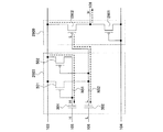
図1(a)に示すレベルシフタは、回路101、回路102を有している。 The level shifter illustrated in FIG. 1A includes a circuit 101 and a circuit 102.
図1(a)のレベルシフタに示すように、回路101は、配線103、配線104、配線105、配線106、配線107、配線108に接続されている。回路102は、配線103、配線104、配線107、配線108、配線109に接続されている。
As shown in the level shifter of FIG. 1A, the circuit 101 is connected to a
なお、配線103及び配線104には、正電源VDD及び負電源VSSがそれぞれ供給されている。また、電源電位VDDは、電源電位VSSよりも高い電圧である。
Note that a positive power supply VDD and a negative power supply VSS are supplied to the
また、配線105及び配線106には、信号(以下、入力信号ともいう)が供給されている。なお、回路101は、配線105及び配線106に供給される信号によって制御されている。
In addition, a signal (hereinafter also referred to as an input signal) is supplied to the
また、配線107及び配線108には、回路101からの信号(以下、オフセット信号ともいう)が供給されている。なお、回路102は、配線107及び配線108に供給される信号によって制御されている。
A signal from the circuit 101 (hereinafter also referred to as an offset signal) is supplied to the
また、配線109には、回路102からの信号(以下、出力信号ともいう)が供給されている。
Further, a signal from the circuit 102 (hereinafter also referred to as an output signal) is supplied to the
なお、配線105及び配線106に供給される信号は、2値の値を持つデジタル信号である。これらのデジタル信号の電位は、H信号(以下、Hレベルともいう)のときには電位VHであり、L信号(以下、Lレベルともいう)のときには電位VLである。なお、電位VHは、電源電位VDDよりも低く、電位VLよりも高い電圧である。なお、電位VLは、電源電位VSSよりも高く、電位VHよりも低い電位である。つまり、各電源電位と信号の電位の関係は、電源電位VDD>電位VH>電位VL>電源電位VSSとなっている。
Note that signals supplied to the
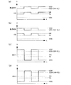
次に、図1(a)で示したレベルシフタの動作について、図2(a)のタイミングチャートを参照して説明する。なお、図2(a)のタイミングチャートは、配線105の信号、配線107の信号、及び配線108の信号を示している。なお、図示はしないが、配線106の信号は、配線105の信号に対して、Hレベル、Lレベルが反転したものと同様である。
Next, the operation of the level shifter shown in FIG. 1A will be described with reference to the timing chart of FIG. Note that the timing chart in FIG. 2A shows a signal of the
ここで、回路101は、オフセット動作をする機能を有する。具体的には、回路101は、配線105及び配線106に供給されている入力信号をオフセットして、配線107、及び配線108にオフセット信号を供給する。このオフセット信号は、配線105に供給されている信号と同じタイミング(若しくは反転)であり、おおむね等しい振幅電圧である。そして、配線107に供給するオフセット信号は、入力信号に対して電位がH側にシフトしている。また、配線108に供給するオフセット信号は、入力信号に対して電位がL側にシフトしている。なお、回路101をオフセット回路ともいう。
Here, the circuit 101 has a function of performing an offset operation. Specifically, the circuit 101 offsets an input signal supplied to the
よって、図2(a)のタイミングチャートに示すように、配線107の信号は、配線105の信号と比較して、タイミング、及び振幅電圧が配線105の信号とおおむね等しく、電位がH側にシフトしている。具体的には、配線107の信号は、L信号の電位がVDDであり、H信号の電位がVDD+(VH−VL)である。つまり、配線107の信号の振幅電圧はVH−VLであり、配線105の信号の振幅電圧とおおむね同じである。
Therefore, as shown in the timing chart of FIG. 2A, the signal of the
配線107の信号と同様に、配線108の信号は、配線105の信号と比較して、タイミング、及び振幅電圧が配線105の信号とおおむね同じであり、電位がL側にシフトしている。具体的には、配線108の信号は、L信号の電位がVSSであり、H信号の電位がVSS+(VH−VL)である。つまり、配線108の信号の振幅電圧はVH−VLであり、配線105の信号の振幅電圧とおおむね同じである。
Similar to the signal of the
なお、すでに述べたように、配線107の信号、及び配線108の信号は、配線105の信号と比較して、H信号、L信号が反転していてもよい。
Note that as described above, the signal of the
なお、図2(b)に示すように、配線107の信号は、L信号をVDD−(VH−VL)、H信号をVDDとしてもよい。また、配線108の信号は、L信号をVSS−(VH−VL)としてもよい。図2(b)に示す場合でも、配線107の信号の振幅電圧、及び配線108の信号の振幅電圧は、VH−VLであり、配線105の信号の振幅電圧とおおむね同じである。
2B, the signal of the
なお、図2(b)に示す配線107の信号、及び配線108の信号も、配線105の信号と比較して、H信号・L信号が反転していてもよい。
Note that the signal of the
ここで、回路102は、インバータ、NAND回路、NOR回路などの論理回路である。具体的には、回路102は、オフセット信号によって制御され、配線109に出力信号を供給する。また、出力信号の電位は、H信号のときには電源電位VDDと等しく、L信号のときには電源電位VSSと等しい。
Here, the circuit 102 is a logic circuit such as an inverter, a NAND circuit, or a NOR circuit. Specifically, the circuit 102 is controlled by the offset signal and supplies an output signal to the
なお、配線107の信号、及び配線108の信号は振幅電圧が小さいため、回路102は貫通電流が少なくなるため省電力化を実現できる。また、回路102は、入力される信号の振幅電圧が小さいためノイズを低減できる。
Note that since the amplitude voltage of the signal of the
以上説明したように、本発明のレベルシフタは、オフセット信号によって、論理回路を駆動することで、レベルシフタとしての機能を実現する。また、本発明のレベルシフタは、省電力であり、低ノイズである。また、本発明のレベルシフタは、1つのレベルシフタによって、入力信号のHレベル、及びLレベルを同時にレベルシフトできる。 As described above, the level shifter of the present invention realizes a function as a level shifter by driving a logic circuit with an offset signal. In addition, the level shifter of the present invention is power saving and low noise. The level shifter of the present invention can simultaneously shift the H level and the L level of the input signal with one level shifter.
なお、図1(b)に示すように、回路102は、配線105の信号、及び配線106の信号をH側にシフトした信号(配線107の信号)だけで、制御されていてもよい。また、回路102が配線107の信号だけで制御される場合、回路101には、電源電位VSSを供給しなくてもよい。
Note that as illustrated in FIG. 1B, the circuit 102 may be controlled only by a signal of the
同様に、図1(c)に示すように、回路102は、配線105の信号、及び配線106の信号をL側だけにシフトした信号(配線108の信号)だけで、制御されていてもよい。また、回路102が配線108の信号だけで制御される場合、回路101には、電源電位VDDを供給しなくてもよい。
Similarly, as illustrated in FIG. 1C, the circuit 102 may be controlled only by the signal of the
また、回路102が配線107の信号、若しくは配線108の信号だけで制御されることによって、図1(b)、及び図1(c)のレベルシフタは回路101を簡単な構成にできる。
Further, when the circuit 102 is controlled only by the signal of the
なお、本実施形態は、本明細書中の他の実施形態のいかなる記載とも自由に組み合わせて実施することができる。また、本実施形態中のいかなる記載も自由に組み合わせて実施することができる。 Note that this embodiment mode can be freely combined with any description in other embodiment modes in this specification. In addition, any description in the present embodiment can be implemented in any combination.
(第2の実施形態)
本実施形態では、第1の実施形態に示したレベルシフタが有する回路101(オフセット回路)の構成例について説明する。なお、本実施形態では、配線105、及び配線106に供給される信号を、同じタイミング(若しくは反転)、及びおおむね等しい振幅電圧のまま、電位をH側にシフトさせて、配線107に供給する場合の構成例について説明する。
(Second Embodiment)
In this embodiment, a configuration example of the circuit 101 (offset circuit) included in the level shifter shown in the first embodiment will be described. In this embodiment, the signal supplied to the
なお、実施の形態1と同様のものに関しては共通の符号を用いて示し、同一部分又は同様な機能を有する部分の詳細な説明は省略する。
Note that components similar to those in
まず、オフセット回路の構成例を図3(a)を参照して説明する。 First, a configuration example of the offset circuit will be described with reference to FIG.
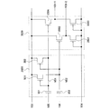
図3(a)に示すオフセット回路は、容量素子301、容量素子302、トランジスタ303、及びトランジスタ304を有している。
The offset circuit illustrated in FIG. 3A includes a
図3(a)のオフセット回路に示すように、容量素子301の第1電極が配線105に接続されている。容量素子302の第1電極が配線106に接続されている。トランジスタ303のゲートが容量素子301の第2電極に接続され、第1端子が配線103に接続され、第2端子が容量素子302の第2電極に接続されている。トランジスタ304のゲートが容量素子302の第2電極に接続され、第1端子が配線103に接続され、第2端子が容量素子301の第2電極に接続されている。なお、容量素子301の第2電極、トランジスタ303のゲート、及びトランジスタ304の第2端子の接続点を節点N31とする。なお、容量素子302の第2電極、トランジスタ303の第2端子、及びトランジスタ304のゲートの接続点を節点N32とする。なお、節点N31と節点N32のうちのどちらかが、図1に示す配線107(a)に接続されている。
As shown in the offset circuit in FIG. 3A, the first electrode of the
次に、図3(a)で示したオフセット回路の動作について、図3(b)、及び図3(c)を参照して説明する。 Next, the operation of the offset circuit shown in FIG. 3A will be described with reference to FIGS. 3B and 3C.
なお、図3(b)は、配線105の信号がH信号からL信号、配線106の信号がL信号からH信号に変化した場合の図3(a)のオフセット回路の動作を示している。
3B shows the operation of the offset circuit in FIG. 3A when the signal of the
また、図3(c)は、配線105の信号がL信号からH信号、配線106の信号がH信号からL信号に変化した場合の図3(a)のオフセット回路の動作を示している。つまり、図3(a)のオフセット回路は、図3(b)の動作と図3(c)の動作を任意のタイミングで繰り返している。また、図3(b)の動作を第1の動作とし、図3(c)の動作を第2の動作とする。
FIG. 3C shows the operation of the offset circuit in FIG. 3A when the signal of the
なお、VH−VLは、トランジスタ303、及びトランジスタ304のしきい値電圧以上である。
Note that VH−VL is higher than or equal to the threshold voltages of the
まず、図3(a)のオフセット回路の第1の動作について、図3(b)を参照して説明する。なお、節点N32の初期値の電位をVDDとする。 First, the first operation of the offset circuit of FIG. 3A will be described with reference to FIG. Note that the initial potential of the node N32 is VDD.
初期状態として、容量素子302には、配線106の電位VL(L信号)と、節点N32の電位VDDとの電位差VDD−VLが保持されている。そして、配線106の電位がVLからVHに変化すると、節点N32の電位は容量素子302の容量結合によってVDD+(VH−VL)となる。したがって、トランジスタ304がオンする。
As an initial state, the
また、トランジスタ304がオンすることによって、節点N31には電源電位VDDが供給され、節点N31の電位がVDDになる。したがって、容量素子301は、配線105の電位VL(L信号)と、節点N31の電位VDDとの電位差VDD−VLを保持する。また、トランジスタ303がオフする。
When the
また、トランジスタ303がオフすることで、節点N32はフローティング状態になり、節点N32は電位をVDD+(VH−VL)に維持する。
Further, when the
次に、図3(a)のオフセット回路の第2の動作について、図3(c)を参照して説明する。 Next, the second operation of the offset circuit of FIG. 3A will be described with reference to FIG.
すでに述べたように、容量素子301には、第1の動作によって、VDD−VLが保持されている。そして、配線105の電位がVLからVHに変化すると、節点N31の電位は容量素子301の容量結合によって、VDD+(VH−VL)となる。したがって、トランジスタ303がオンする。
As already described, VDD-VL is held in the
また、トランジスタ303がオンすることによって、節点N32には電源電位VDDが供給され、節点N32の電位がVDDになる。したがって、容量素子302は、配線106の電位VL(L信号)と、節点N32の電位VDDとの電位差VDD−VLを保持する。また、トランジスタ304がオフする。
When the
また、トランジスタ304がオフすることで、節点N31はフローティング状態になり、節点N31は電位をVDD+(VH−VL)に維持する。
Further, when the
ここで、容量素子301、容量素子302、トランジスタ303、及びトランジスタ304が有する機能について説明する。
Here, functions of the
まず、容量素子301は、第1の動作において、配線105の電位VLと、節点N31の電位VDDとの電位差を保持する。そして、容量素子301は、第2の動作において、容量結合によって、配線105の電位の上昇にしたがって、節点N31の電位を上昇させる機能を有する。
First, in the first operation, the
また、容量素子302は、第2の動作において、配線106の電位VLと、節点N32の電位VDDとの電位差を保持する。そして、容量素子302は、第1の動作において、容量結合によって、配線106の電位の上昇にしたがって、節点N32の電位を上昇させる機能を有する。
Further, in the second operation, the
また、トランジスタ303は、節点N31の電位によって、配線103と節点N32とを接続するかしないかを選択するスイッチとしての機能を有する。また、トランジスタ303は、第1の動作において、オフし、節点N32をフローティング状態にする。また、トランジスタ303は、第2の動作において、オンし、節点N32に電源電位VDDを供給する。
The
また、トランジスタ304は、節点N32の電位によって、配線103と節点N31とを接続するかしないかを選択するスイッチとしての機能を有する。また、トランジスタ304は、第1の動作において、オンし、節点N31に電源電位VDDを供給する。また、トランジスタ304は、第2の動作において、オフし、節点N31をフローティング状態にする。
The
以上説明した第1の動作、及び第2の動作によって、図3(a)のオフセット回路は、第1の動作において、節点N31には電源電位VDDを供給し、節点N32をフローティング状態にし、節点N32の電位をVDD+(VH−VL)に維持するように動作する。また、図3(a)のオフセット回路は、第2の動作において、節点N31をフローティング状態にし、節点N31の電位をVDD+(VH−VL)に維持し、節点N32には電源電位VDDを供給するように動作する。 By the first operation and the second operation described above, in the first operation, the offset circuit in FIG. 3A supplies the power supply potential VDD to the node N31, sets the node N32 in a floating state, and It operates so as to maintain the potential of N32 at VDD + (VH−VL). Further, in the second operation, the offset circuit of FIG. 3A places the node N31 in a floating state, maintains the potential of the node N31 at VDD + (VH−VL), and supplies the power supply potential VDD to the node N32. To work.
したがって、図3(a)のオフセット回路が生成する信号は、H信号がVDD+(VH−VL)であり、L信号がVDDである。つまり、図3(a)のオフセット回路は、電源電位VDDを基準とした信号を生成することができる。 Therefore, in the signal generated by the offset circuit of FIG. 3A, the H signal is VDD + (VH−VL) and the L signal is VDD. That is, the offset circuit in FIG. 3A can generate a signal based on the power supply potential VDD.
なお、第1の動作における節点N32の電位、及び第2の動作における節点N31の電位は、VDD+(VH−VL)を維持するとした。しかし、実際には、第1の動作における節点N32の電位、及び第2の動作における節点N31の電位は、配線容量や寄生容量の影響などによって、VDD+(VH−VL)よりも低くなる。したがって、配線容量や寄生容量の影響を少なくするために、容量素子301、及び容量素子302の容量値は、配線容量や寄生容量の容量値よりも十分大きくしておけばよい。
Note that the potential of the node N32 in the first operation and the potential of the node N31 in the second operation are maintained at VDD + (VH−VL). However, in reality, the potential of the node N32 in the first operation and the potential of the node N31 in the second operation are lower than VDD + (VH−VL) due to the influence of wiring capacitance and parasitic capacitance. Therefore, in order to reduce the influence of the wiring capacitance and the parasitic capacitance, the capacitance values of the
なお、節点N31を図1(a)に示す配線107に接続すれば、配線105に供給されている信号とHレベル、Lレベルが同じ信号を配線107に供給することができる。同様に、節点N32を図1に示す配線107に接続すれば、配線105に供給されている信号とH信号、L信号が反転した信号を配線107に供給することができる。
Note that if the node N31 is connected to the
また、節点N31を配線107に接続する場合には、容量素子302の容量値は、容量素子301の容量値よりも小さいことが好ましい。なぜなら、すでに述べたように、容量素子301の容量値は、配線容量や寄生容量の容量値よりも十分大きくしておけばよいと説明したが、節点N32の電位はトランジスタ304をオンできれば、節点N32の電位はVDD+(VH−VL)にならなくてもよいからである。したがって、容量素子302の容量値を容量素子301の容量値よりも小さくできるため、容量素子302の素子領域を小さくできる。
In the case where the node N31 is connected to the
また、節点N32を配線107に接続する場合には、節点N31を配線107に接続する場合と同様の理由で、容量素子301の容量値は容量素子302の容量値よりも小さくすることが好ましい。
In addition, when the node N32 is connected to the
なお、容量素子301、及び容量素子302は、絶縁層を2つの電極層で挟持した構成でもよい。容量素子301、及び容量素子302を絶縁層を2つの電極層で挟持した構成にすることで、容量素子301、及び容量素子302は印加される電圧に関係なく容量値を一定に保つことができるため、本発明のレベルシフタは安定して動作できる。
Note that the
また、容量素子301、及び容量素子302の絶縁層は、ゲート絶縁膜であることが好ましい。なぜなら、ゲート絶縁膜の膜厚は、一般的に他の絶縁膜(例えば、層間膜、平坦化膜など)に比べ薄いため、容量素子301、及び容量素子302は効率的に容量値を得ることができるからである。
The insulating layer of the
なお、容量素子301、及び容量素子302は、MOS構造の容量素子としてもよい。容量素子301、及び容量素子302をMOS構造の容量素子とした場合の構成を図4(a)に示す。図4(a)に示すオフセット回路は、容量素子301の代わりにNチャネル型のトランジスタ401を用い、容量素子302の代わりにNチャネル型のトランジスタ402を用いている。また、トランジスタ401は、ゲートが節点N31に接続され、第1端子、及び第2端子が配線105に接続されていることを特徴とする。なぜなら、節点N31の電位は配線105の電位よりも高いため、トランジスタ401がオンして、チャネルがトランジスタ401のチャネル領域に形成されるため、トランジスタ401は容量素子として動作できるからである。同様に、トランジスタ402は、ゲートが節点N32に接続され、第1端子、及び第2端子が配線106に接続されていることを特徴とする。なぜなら、節点N32電位は配線106の電位よりも高いため、トランジスタ402がオンして、チャネルがトランジスタ402のチャネル領域に形成されるため、トランジスタ402は容量素子として動作できるからである。
Note that the
また、図4(b)のように、容量素子として、Pチャネル型のトランジスタを容量素子として用いることもできる。図4(b)に示すオフセット回路は、容量素子301の代わりにPチャネル型のトランジスタ403を用い、容量素子302の代わりにPチャネル型のトランジスタ404を用いている。また、トランジスタ403は、ゲートが配線105に接続され、第1端子、及び第2端子が節点N31に接続されていることを特徴とする。なぜなら、節点N31の電位は、配線105の電位よりも高いため、トランジスタ403がオンして、チャネルがトランジスタ403のチャネル領域に形成されるため、トランジスタ403が容量素子として動作できるからである。同様に、トランジスタ404は、ゲートが配線106に接続され、第1端子、及び第2端子が節点N32に接続されていることを特徴とする。なぜなら、節点N32の電位は配線106の電位よりも高いため、トランジスタ404がオンして、チャネルがトランジスタ404のチャネル領域に形成されるため、トランジスタ404は容量素子として動作できるからである。
As shown in FIG. 4B, a P-channel transistor can be used as the capacitor as the capacitor. The offset circuit illustrated in FIG. 4B uses a P-
なお、すでに述べたように、図4(a)において、節点N31を配線107に接続する場合には、トランジスタ401のチャネル領域(L:チャネル長×W:チャネル幅)よりも、トランジスタ402のチャネル領域のほうが小さいことが好ましい。また、節点N32を配線107に接続する場合には、トランジスタ401のチャネル領域よりも、トランジスタ402のチャネル領域のほうが大きいほうが好ましい。
4A, when the node N31 is connected to the
また、同様に、図4(b)において、節点N31を配線107に接続する場合には、トランジスタ403のチャネル領域(L:チャネル長×W:チャネル幅)よりも、トランジスタ404のチャネル領域のほうが小さいことが好ましい。また、節点N32を配線107に接続する場合には、トランジスタ403のチャネル領域よりも、トランジスタ404のチャネル領域のほうが大きいほうが好ましい。
Similarly, in FIG. 4B, when the node N31 is connected to the
ここで、図3(a)に示したオフセット回路は、Nチャネル型のトランジスタと容量素子とで構成したが、Pチャネル型のトランジスタと容量素子とで構成されていてもよい。Pチャネル型のトランジスタと容量素子とで構成した場合のオフセット回路を図5(a)に示す。 Here, the offset circuit illustrated in FIG. 3A is configured with an N-channel transistor and a capacitor, but may be configured with a P-channel transistor and a capacitor. FIG. 5A shows an offset circuit in the case where it is configured by a P-channel transistor and a capacitor.
図5(a)に示すオフセット回路は、容量素子301、容量素子302、トランジスタ501、及びトランジスタ502を有している。
The offset circuit illustrated in FIG. 5A includes a
なお、トランジスタ501、及びトランジスタ502は、図3(a)のトランジスタ303、及びトランジスタ304に、それぞれ対応し、それぞれ同様な機能を有する。また、節点N51、及び節点N52は、図3(a)のトランジスタ節点N31、及び節点N32に、それぞれ対応している。
Note that the
図5(a)のオフセット回路に示すように、容量素子301の第1電極が配線105に接続されている。容量素子302の第1電極が配線106に接続されている。トランジスタ501のゲートが容量素子301の第2電極に接続され、第1端子が配線103に接続され、第2端子が容量素子302の第2電極に接続されている。トランジスタ502のゲートが容量素子302の第2電極に接続され、第1端子が配線103に接続され、第2端子が容量素子301の第2電極に接続されている。なお、容量素子301の第2電極、トランジスタ501のゲート、及びトランジスタ502の第2端子の接続点を節点N51とする。なお、容量素子302の第2電極、トランジスタ501の第2端子、及びトランジスタ502のゲートの接続点を節点N52とする。なお、節点N51と節点N52のうちのどちらかが、図1(a)に示す配線107に接続されている。
As shown in the offset circuit of FIG. 5A, the first electrode of the
次に、図5(a)で示したオフセット回路の動作について、図5(b)、及び図5(c)を参照して説明する。 Next, the operation of the offset circuit shown in FIG. 5A will be described with reference to FIGS. 5B and 5C.
なお、図5(b)は、配線105の信号がH信号からL信号、配線106の信号がL信号からH信号に変化した場合の図5(a)のオフセット回路の動作を示している。
FIG. 5B shows the operation of the offset circuit in FIG. 5A when the signal of the
また、図5(c)は、配線105の信号がL信号からH信号、配線106の信号がH信号からL信号に変化した場合の図5(a)のオフセット回路の動作を示している。つまり、図5(a)のオフセット回路は、図5(b)の動作と図5(c)の動作を任意のタイミングで繰り返している。また、図5(b)の動作を第1の動作とし、図5(c)の動作を第2の動作とする。
5C shows the operation of the offset circuit in FIG. 5A when the signal of the
まず、図5(a)のオフセット回路の第1の動作について、図5(b)を参照して説明する。なお、節点N51の初期値の電位をVDDとする。 First, the first operation of the offset circuit of FIG. 5A will be described with reference to FIG. Note that the initial potential of the node N51 is VDD.
初期状態として、容量素子301には、配線105の電位VH(H信号)と、節点N51の電位VDDとの電位差VDD−VHが保持されている。そして、配線105の電位がVHからVLに変化すると、節点N51の電位は容量素子301の容量結合によってVDD−(VH−VL)となる。したがって、トランジスタ501がオンする。
As an initial state, the
また、トランジスタ501がオンするとによって、節点N52には電源電位VDDが供給され、節点N52の電位がVDDになる。したがって、容量素子302は、配線106の電位VH(H信号)と、節点N52の電位VDDとの電位差VDD−VHを保持する。また、トランジスタ502がオフする。
When the
また、トランジスタ502がオフすることによって、節点N51はフローティング状態になり、節点N51は電位VDD−(VH−VL)を維持する。
Further, when the
次に、図5(a)のオフセット回路の第2の動作について、図5(c)を参照して説明する。 Next, the second operation of the offset circuit of FIG. 5A will be described with reference to FIG.
すでに述べたように、容量素子302には、第1の動作によって、VDD−VHが保持されている。そして、配線106の電位がVHからVLに変化すると、節点N52の電位は容量素子302の容量結合によって、VDD−(VH−VL)となる。したがって、トランジスタ502がオンする。
As already described, VDD-VH is held in the
また、トランジスタ502がオンすることによって、節点N51には電源電位VDDが供給され、節点N51の電位がVDDになる。したがって、容量素子301は、配線105の電位VH(H信号)と、節点N51の電位VDDとの電位差VDD−VHを保持する。また、トランジスタ501がオフする。
When the
また、トランジスタ501がオフすることで、節点N52がフローティング状態になり、節点N52は電位をVDD−(VH−VL)に維持する。
Further, when the
以上説明した第1の動作、及び第2の動作によって、図5(a)のオフセット回路は、第1の動作において、節点N51をフローティング状態にし、節点N51の電位をVDD−(VH−VL)に維持し、節点N52には電源電位VDDを供給するように動作する。また、図5(a)のオフセット回路は、第2の動作において、節点N51には電源電位VDDを供給し、節点N52をフローティング状態にし、節点N52の電位をVDD−(VH−VL)に維持するように動作する。 By the first operation and the second operation described above, the offset circuit in FIG. 5A causes the node N51 to be in a floating state and the potential of the node N51 to be VDD− (VH−VL) in the first operation. And the node N52 operates to supply the power supply potential VDD. In the second operation, the offset circuit in FIG. 5A supplies the power supply potential VDD to the node N51, sets the node N52 in a floating state, and maintains the potential of the node N52 at VDD− (VH−VL). To work.
したがって、図5(a)のオフセット回路が生成する信号は、H信号がVDDであり、L信号がVDD−(VH−VL)である。つまり、図5(a)の回路101は、電源電位VDDを基準とした信号を生成することができる。 Therefore, in the signal generated by the offset circuit of FIG. 5A, the H signal is VDD and the L signal is VDD− (VH−VL). That is, the circuit 101 in FIG. 5A can generate a signal based on the power supply potential VDD.
なお、図3(a)のオフセット回路と同様に、図5(a)のオフセット回路が生成する信号は、L信号の電位をVDD−(VH−VL)としたが、実際には、VDD−(VH−VL)よりも少し高くなっている。 As in the offset circuit of FIG. 3A, the signal generated by the offset circuit of FIG. 5A has the L signal potential VDD− (VH−VL). It is slightly higher than (VH-VL).
なお、図3(a)のオフセット回路と同様に、節点N51を図1(a)に示す配線107に接続すれば、配線105に供給されている信号とHレベルLレベルが同じ信号を配線107に供給することができる。同様に、節点N52を図1(a)に示す配線107に接続すれば、配線105に供給されている信号とH信号、L信号が反転した信号を配線107に供給することができる。
3A, if the node N51 is connected to the
また、図3(a)のオフセット回路と同様に、節点N51を配線107に接続する場合には、容量素子302の容量値は、容量素子301の容量値よりも小さいことが好ましい。
3A, in the case where the node N51 is connected to the
また、図3(a)のオフセット回路と同様に、節点N52を配線107に接続する場合には、容量素子301の容量値は容量素子302の容量値よりも小さくすることが好ましい。
3A, when the node N52 is connected to the
なお、図4のオフセット回路と同様に、容量素子301、及び容量素子302はMOS構造の容量素子としてもよい。図6(a)に示すように、容量素子301の代わりにPチャネル型のトランジスタ601を用い、容量素子302の代わりにPチャネル型のトランジスタ602を用いてもよい。また、トランジスタ601のゲートが配線105に接続され、第1端子、及び第2端子が節点N51に接続されていることを特徴とする。同様に、トランジスタ602のゲートが配線106に接続され、第1端子、及び第2端子が節点N52に接続されていることを特徴とする。
Note that as in the offset circuit in FIG. 4, the
また、図4のオフセット回路と同様に、図6(b)のように、容量素子301、及び容量素子302として、Nチャネル型のトランジスタ603、及びNチャネル型のトランジスタ604を、それぞれ用いることもできる。また、トランジスタ603のゲートが節点N51に接続され、第1端子、及び第2端子が配線105に接続されていることを特徴とする。同様に、トランジスタ604のゲートが節点N52に接続され、第1端子、及び第2端子が配線106に接続されていることを特徴とする。
Similarly to the offset circuit in FIG. 4, an N-
なお、図4と同様に、図6(a)において、節点N51を配線107に接続する場合には、トランジスタ601のチャネル領域よりも、トランジスタ602のチャネル領域のほうが小さいことが好ましい。また、節点N52を配線107に接続する場合には、トランジスタ601のチャネル領域よりも、トランジスタ602のチャンネル領域のほうが大きいことが好ましい。
4A, in the case where the node N51 is connected to the
また、同様に、図6(b)において、節点N51を配線107に接続する場合には、トランジスタ603のチャネル領域よりも、トランジスタ604のチャネル領域のほうが小さいことが好ましい。また、節点N52を配線107に接続する場合には、トランジスタ603のチャネル領域よりも、トランジスタ604のチャンネル領域のほうが大きいことが好ましい。
Similarly, in FIG. 6B, in the case where the node N51 is connected to the
なお、本実施形態は、本明細書中の他の実施形態のいかなる記載とも自由に組み合わせて実施することができる。また、本実施形態中のいかなる記載も自由に組み合わせて実施することができる。 Note that this embodiment mode can be freely combined with any description in other embodiment modes in this specification. In addition, any description in the present embodiment can be implemented in any combination.
(第3の実施形態)
本実施形態では、第1の実施形態に示したレベルシフタが有する回路101(オフセット回路)の構成例について説明する。なお、本実施形態では、配線105、及び配線106に供給される信号を、同じタイミング(若しくは反転)、及びおおむね等しい振幅電圧のまま、電位をL側にシフトさせて、配線108に供給する場合の構成例について説明する。
(Third embodiment)
In this embodiment, a configuration example of the circuit 101 (offset circuit) included in the level shifter shown in the first embodiment will be described. Note that in this embodiment, the signal supplied to the
なお、第1の実施形態、及び第2の実施形態と同様のものに関しては共通の符号を用いて示し、同一部分又は同様な機能を有する部分の詳細な説明は省略する。 Note that components similar to those in the first embodiment and the second embodiment are denoted by common reference numerals, and detailed description of the same portions or portions having similar functions is omitted.
まず、オフセット回路の構成例を図7(a)を参照して説明する。 First, a configuration example of the offset circuit will be described with reference to FIG.
図7(a)に示すオフセット回路は、容量素子701、容量素子702、トランジスタ703、及びトランジスタ704を有している。
The offset circuit illustrated in FIG. 7A includes a
図7(a)のオフセット回路に示すように、容量素子701の第1電極が配線105に接続されている。容量素子702の第1電極が配線106に接続されている。トランジスタ703のゲートが容量素子701の第2電極に接続され、第1端子が配線104に接続され、第2端子が容量素子702の第2電極に接続されている。トランジスタ704のゲートが容量素子702の第2電極に接続され、第1端子が配線104に接続され、第2端子が容量素子701の第2電極に接続されている。なお、容量素子701の第2電極、トランジスタ703のゲート、及びトランジスタ704の第2端子の接続点を節点N71とする。なお、容量素子702の第2電極、トランジスタ703の第2端子、及びトランジスタ704のゲートの接続点を節点N72とする。なお、節点N71と節点N72のうちどちらかが、図1(a)に示す配線108に接続されている。
As shown in the offset circuit in FIG. 7A, the first electrode of the
次に、図7(a)で示したオフセット回路の動作について、図7(b)、及び図7(c)を参照して説明する。 Next, the operation of the offset circuit shown in FIG. 7A will be described with reference to FIGS. 7B and 7C.
なお、図7(b)は、配線105の信号がH信号からL信号、配線106の信号がL信号からH信号に変化した場合の図7(a)の動作を示している。
FIG. 7B shows the operation of FIG. 7A when the signal of the
また、図7(c)は、配線105の信号がL信号からH信号、配線106の信号がH信号からL信号に変化した場合の図7(a)のオフセット回路の動作を示している。つまり、図7(a)のオフセット回路は、図7(b)の動作と図7(c)の動作を任意のタイミングで繰り返している。また、図7(b)の動作を第1の動作とし、図7(c)の動作を第3の動作とする。
FIG. 7C shows the operation of the offset circuit in FIG. 7A when the signal of the
なお、VH−VLは、トランジスタ703、及びトランジスタ704のしきい値電圧以上である。
Note that VH−VL is higher than or equal to the threshold voltage of the
まず、図7(a)のオフセット回路の第1の動作について、図7(b)を参照して説明する。なお、節点N72の初期値の電位をVSSとする。 First, the first operation of the offset circuit of FIG. 7A will be described with reference to FIG. Note that the initial potential of the node N72 is VSS.
初期状態として、容量素子702には、配線106の電位VL(L信号)と、節点N72の電位VSSとの電位差VL−VSSが保持されている。そして、配線106の電位がVLからVHに変化すると、節点N72の電位は容量素子702の容量結合によって、VSS+(VH−VL)となる。したがって、トランジスタ704がオンする。
As an initial state, the
また、トランジスタ704がオンすることによって、節点N71には電源電位VSSが供給され、節点N71の電位がVSSになる。したがって、容量素子701は、配線105の電位VL(L信号)と、節点N71の電位VSSとの電位差VL−VSSを保持する。また、トランジスタ703がオフする。
Further, when the
また、トランジスタ703がオフすることで、節点N72はフローティング状態になり、節点N72は電位をVSS+(VH−VL)に維持する。
Further, when the
次に、図7(a)のオフセット回路の第2の動作について、図7(c)を参照して説明する。 Next, the second operation of the offset circuit of FIG. 7A will be described with reference to FIG.
すでに述べたように、容量素子701には、第1の動作によって、VL−VSSが保持されている。そして、配線105の電位がVLからVHに変化すると、節点N71の電位は容量素子701の容量結合によって、VSS+(VH−VL)となる。したがって、トランジスタ703がオンする。
As already described, VL-VSS is held in the
また、トランジスタ703がオンすることによって、節点N72には電源電位VSSが供給され、節点N72の電位がVSSになる。したがって、容量素子702は、配線106の電位VL(L信号)と、節点N72の電位VSSとの電位差VL−VSSを保持する。また、トランジスタ704がオフする。
Further, when the
また、トランジスタ704がオフすることで、節点N71はフローティング状態になり、節点N71は電位をVSS+(VH−VL)に維持する。
Further, when the
ここで、容量素子701、容量素子702、トランジスタ703、及びトランジスタ704が有する機能について説明する。
Here, functions of the
まず、容量素子701は、第1の動作において、配線105の電位VLと、節点N71の電位VSSとの電位差を保持する。そして、容量素子701は、第2の動作において、容量結合によって、配線105の電位の上昇にしたがって、節点N71の電位を上昇させる機能を有する。
First, in the first operation, the
また、容量素子702は、第2の動作において、配線106の電位VLと、節点N72の電位VSSとの電位差を保持する。そして、容量素子702は、第1の動作において、容量結合によって、配線106の電位の上昇にしたがって、節点N72の電位を上昇させる機能を有する。
In the second operation, the
また、トランジスタ703は、節点N71の電位によって、配線104と節点N72とを接続するかしないかを選択するスイッチとしての機能を有する。また、トランジスタ703は、第1の動作において、オフし、節点N72をフローティング状態にする。また、トランジスタ703は、第2の動作において、オンし、節点N72に電源電位VSSを供給する。
The
また、トランジスタ704は、節点N72の電位によって、配線104と節点N71とを接続するかしないかを選択するスイッチとしての機能を有する。また、トランジスタ704は、第1の動作において、オンし、節点N71に電源電位VSSを供給する。また、トランジスタ704は、第2の動作において、オフし、節点N71をフローティング状態にする。
The
以上説明した第1の動作、及び第2の動作によって、図7(a)のオフセット回路は、第1の動作において、節点N71には電源電位VSSを供給し、節点N72をフローティング状態にし、節点N72の電位をVSS+(VH−VL)に維持するように動作する。また、図7(a)の回路101は、第2の動作において、節点N71をフローティング状態にし、節点N71の電位をVSS+(VH−VL)に維持し、節点N72には電源電位VSSを供給するように動作する。 By the first operation and the second operation described above, in the first operation, the offset circuit in FIG. 7A supplies the power supply potential VSS to the node N71, sets the node N72 in a floating state, and It operates so as to maintain the potential of N72 at VSS + (VH−VL). In the second operation, the circuit 101 in FIG. 7A places the node N71 in a floating state, maintains the potential of the node N71 at VSS + (VH−VL), and supplies the power supply potential VSS to the node N72. To work.
したがって、図7(a)のオフセット回路が生成する信号は、H信号がVSS+(VH−VL)であり、L信号がVSSである。つまり、図7(a)のオフセット回路は、電源電位VSSを基準とした信号を生成することができる。 Therefore, in the signal generated by the offset circuit in FIG. 7A, the H signal is VSS + (VH−VL) and the L signal is VSS. That is, the offset circuit in FIG. 7A can generate a signal based on the power supply potential VSS.
なお、第1の動作における節点N72の電位、及び第2の動作における節点N71の電位は、VSS+(VH−VL)を維持するとした。しかし、実際には、第1の動作における節点N72の電位、及び第2の動作における節点N71の電位は、配線容量や寄生容量の影響などによって、VSS+(VH−VL)よりも低くなる。したがって、配線容量や寄生容量の影響を少なくするために、容量素子701、及び容量素子702の容量値は、配線容量や寄生容量の容量値よりも十分大きくしておけばよい。
Note that the potential of the node N72 in the first operation and the potential of the node N71 in the second operation are maintained at VSS + (VH−VL). However, in reality, the potential of the node N72 in the first operation and the potential of the node N71 in the second operation are lower than VSS + (VH−VL) due to the influence of wiring capacitance and parasitic capacitance. Therefore, in order to reduce the influence of the wiring capacitance and the parasitic capacitance, the capacitance values of the
なお、節点N71を図1(a)に示す配線108に接続すれば、配線105に供給されている信号とH信号、L信号が同じ信号を配線108に供給することができる。同様に、節点N72を図1(a)に示す配線108に接続すれば、配線105に供給されている信号とH信号、L信号が反転した信号を配線108に供給することができる。
Note that if the node N71 is connected to the
また、節点N71を配線108に接続する場合には、容量素子702の容量値は、容量素子701の容量値よりも小さいことが好ましい。なぜなら、すでに述べたように、容量素子701の容量値は、配線容量や寄生容量の容量値よりも十分大きくしておけばよいと説明したが、節点N72の電位はトランジスタ704をオンできれば、節点N72の電位はVSS+(VH−VL)にならなくてもよいからである。したがって、容量素子702の容量値を容量素子701の容量値よりも小さくできるため、容量素子702の素子領域を小さくできる。
In the case where the node N71 is connected to the
また、節点N72を配線108に接続する場合には、節点N71を配線108に接続する場合と同様の理由で、容量素子701の容量値は容量素子702の容量値よりも小さくすることが好ましい。
In the case where the node N72 is connected to the
なお、容量素子701、及び容量素子702は、絶縁層を2つの電極層で挟持した構成でもよい。容量素子701、及び容量素子702を絶縁層を2つの電極層で挟持した構成にすることで、容量素子701、及び容量素子702は印加される電圧に関係なく容量値を一定に保つことができるため、本発明のレベルシフタは安定して動作できる。
Note that the
また、容量素子701、及び容量素子702の絶縁層は、ゲート絶縁膜であることが好ましい。なぜなら、ゲート絶縁膜の膜厚は、一般的に他の絶縁膜(例えば、層間膜、平坦化膜など)に比べ薄いため、容量素子701、及び容量素子702は効率的に容量値を得ることができるからである。
The insulating layers of the
なお、容量素子701、及び容量素子702は、MOS構造の容量素子としてもよい。容量素子701、及び容量素子702をMOS構造の容量素子とした場合の構成を図8(a)に示す。図8(a)に示すオフセット回路は、容量素子701の代わりにNチャネル型のトランジスタ801を用い、容量素子702の代わりにNチャネル型のトランジスタ802を用いている。また、トランジスタ801は、ゲートが配線105に接続され、第1端子、及び第2端子が節点N71に接続されていることを特徴とする。なぜなら、配線105の電位は節点N71の電位よりも高いため、トランジスタ801がオンして、チャネルがトランジスタ901のチャネル領域に形成されるため、トランジスタ801は容量素子として動作できるからである。同様に、トランジスタ802は、ゲートが配線106に接続され、第1端子、及び第2端子が節点N72に接続されていることを特徴とする。なぜなら、配線N106の電位は節点N72の電位よりも高いため、トランジスタ802がオンして、チャネルがトランジスタ802のチャネル領域に形成されるため、トランジスタ802は容量素子として動作できるからである。
Note that the
また、図8(b)のように、容量素子として、Pチャネル型のトランジスタを容量素子として用いることもできる。図8(b)に示すオフセット回路は、容量素子701の代わりにPチャネル型のトランジスタ803を用い、容量素子702の代わりにPチャネル型のトランジスタ804を用いている。また、トランジスタ803は、ゲートが節点N71に接続され、第1端子、及び第2端子が配線105に接続されていることを特徴とする。なぜなら、節点N71の電位は、配線105の電位よりも低いため、トランジスタ803がオンして、チャネルがトランジスタ803のチャネル領域に形成されるため、トランジスタ803が容量素子として動作する。同様に、トランジスタ804は、ゲートが節点N72に接続され、第1端子、及び第2端子が配線106に接続されていることを特徴とする。なぜなら、節点N72の電位は配線106の電位よりも低いため、トランジスタ804がオンして、チャネルがトランジスタ804のチャネル領域に形成されるため、トランジスタ804は容量素子として動作できるからである。
As shown in FIG. 8B, a P-channel transistor can be used as the capacitor as the capacitor. In the offset circuit illustrated in FIG. 8B, a P-
なお、すでに述べたように、図8(a)において、節点N71を配線108に接続する場合には、トランジスタ801のチャネル領域(L:チャネル長×W:チャネル幅)よりも、トランジスタ802のチャネル領域のほうが小さいことが好ましい。また、節点N72を配線108に接続する場合には、トランジスタ801のチャネル領域よりも、トランジスタ802のチャネル領域のほうが大きいほうが好ましい。
Note that as described above, in FIG. 8A, when the node N71 is connected to the
また、同様に、図8(b)において、節点N71を配線108に接続する場合には、トランジスタ803のチャネル領域(L:チャネル長×W:チャネル幅)よりも、トランジスタ804のチャネル領域のほうが小さいことが好ましい。また、節点N72を配線108に接続する場合には、トランジスタ803のチャネル領域よりも、トランジスタ804のチャネル領域のほうが大きいほうが好ましい。
Similarly, in FIG. 8B, when the node N71 is connected to the
ここで、図7(a)に示したオフセット回路は、Nチャネル型のトランジスタと容量素子とで構成したが、Pチャネル型のトランジスタと容量素子とで構成されていてもよい。Pチャネル型のトランジスタと容量素子とで構成した場合のオフセット回路を図9(a)に示す。 Here, the offset circuit illustrated in FIG. 7A is configured with an N-channel transistor and a capacitor, but may be configured with a P-channel transistor and a capacitor. FIG. 9A shows an offset circuit in the case of being constituted by a P-channel transistor and a capacitor.
図9(a)に示すオフセット回路は、容量素子701、容量素子702、トランジスタ901、及びトランジスタ902を有している。
The offset circuit illustrated in FIG. 9A includes a
なお、トランジスタ901、及びトランジスタ902は、図7(a)のトランジスタ703、及びトランジスタ704に、それぞれ対応し、それぞれ同様な機能を有する。また、節点N91、及び節点N92は、図7(a)のトランジスタ節点N71、及び節点N72に、それぞれ対応している。
Note that the
図9(a)のオフセット回路に示すように、容量素子701の第1電極が配線105に接続されている。容量素子702の第1電極が配線106に接続されている。トランジスタ901のゲートが容量素子701の第2電極に接続され、第1端子が配線104に接続され、第2端子が容量素子702の第2電極に接続されている。トランジスタ902のゲートが容量素子702の第2電極に接続され、第1端子が配線104に接続され、第2端子が容量素子701の第2電極に接続されている。なお、容量素子701の第2電極、トランジスタ901のゲート、及びトランジスタ902の第2端子の接続点を節点N91とする。なお、容量素子702の第2電極、トランジスタ901の第2端子、及びトランジスタ902のゲートの接続点を節点N92とする。なお、節点N91と節点N92のうちのどちらかが、図1(a)に示す配線108に接続されている。
As shown in the offset circuit of FIG. 9A, the first electrode of the
次に、図9(a)で示したオフセット回路の動作について、図9(b)、及び図9(c)を参照して説明する。 Next, the operation of the offset circuit shown in FIG. 9A will be described with reference to FIGS. 9B and 9C.
なお、図9(b)は、配線105の信号がH信号からL信号、配線106の信号がL信号からH信号に変化した場合の図9(a)のオフセット回路の動作を示している。
Note that FIG. 9B shows the operation of the offset circuit in FIG. 9A when the signal of the
また、図9(c)は、配線105の信号がL信号からH信号、配線106の信号がH信号からL信号に変化した場合の図9(a)のオフセット回路の動作を示している。つまり、図9(a)のオフセット回路は、図9(b)の動作と図9(c)の動作を任意のタイミングで繰り返している。また、図9(b)の動作を第1の動作とし、図9(c)の動作を第2の動作とする。
FIG. 9C shows the operation of the offset circuit in FIG. 9A when the signal of the
まず、図9(a)のオフセット回路の第1の動作について、図9(b)を参照して説明する。なお、節点N91の初期値の電位をVSSとする。 First, the first operation of the offset circuit of FIG. 9A will be described with reference to FIG. Note that the initial potential of the node N91 is VSS.
初期状態として、容量素子701には、配線105の電位VH(H信号)と、節点N91の電位VSSとの電位差VH−VSSが保持されている。そして、配線105の電位がVHからVLに変化すると、節点N91の電位は容量素子701の容量結合によってVSS−(VH−VL)となる。したがって、トランジスタ901がオンする。
As an initial state, the
また、トランジスタ901がオンするとによって、節点N92には電源電位VSSが供給され、節点N92の電位がVSSになる。したがって、容量素子702は、配線106の電位VH(H信号)と、節点N92の電位VSSとの電位差VH−VSSを保持する。また、トランジスタ902がオフする。
Further, when the
また、トランジスタ902がオフすることによって、節点N91はフローティング状態になり、節点N91は電位VSS−(VH−VL)を維持する。
Further, when the
次に、図9(a)のオフセット回路の第2の動作について、図9(c)を参照して説明する。 Next, the second operation of the offset circuit of FIG. 9A will be described with reference to FIG.
すでに述べたように、容量素子702には、第1の動作によって、VH−VSSが保持されている。そして、配線106の電位がVHからVLに変化すると、節点N92の電位は容量素子702の容量結合によって、VSS−(VH−VL)となる。したがって、トランジスタ902がオンする。
As already described, VH-VSS is held in the
また、トランジスタ902がオンすることによって、節点N91には電源電位VSSが供給され、節点N91の電位がVSSになる。したがって、容量素子701は、配線105の電位VH(H信号)と、節点N91の電位VSSとの電位差VH−VSSを保持する。また、トランジスタ901がオフする。
Further, when the
また、トランジスタ901がオフすることで、節点N92がフローティング状態になり、節点N92は電位をVSS−(VH−VL)に維持する。
Further, when the
以上説明した第1の動作、及び第2の動作によって、図9(a)のオフセット回路は、第1の動作において、節点N91をフローティング状態にし、節点N91の電位をVSS−(VH−VL)に維持し、節点N92には電源電位VSSを供給するように動作する。また、図9(a)のオフセット回路は、第2の動作において、節点N91には電源電位VSSを供給し、節点N92をフローティング状態にし、節点N92の電位をVSS−(VH−VL)に維持するように動作する。 By the first operation and the second operation described above, the offset circuit of FIG. 9A causes the node N91 to be in a floating state and the potential of the node N91 to be VSS− (VH−VL) in the first operation. And the node N92 operates to supply the power supply potential VSS. In the second operation, the offset circuit in FIG. 9A supplies the power supply potential VSS to the node N91, sets the node N92 in a floating state, and maintains the potential of the node N92 at VSS− (VH−VL). To work.
したがって、図9(a)のオフセット回路が生成する信号は、H信号がVSSであり、L信号がVSS−(VH−VL)である。つまり、図9(a)のオフセット回路は、電源電位VSSを基準とした信号を生成することができる。 Therefore, in the signal generated by the offset circuit in FIG. 9A, the H signal is VSS and the L signal is VSS− (VH−VL). That is, the offset circuit in FIG. 9A can generate a signal based on the power supply potential VSS.
なお、図7(a)のオフセット回路と同様に、図9(a)のオフセット回路が生成する信号は、L信号の電位をVSS−(VH−VL)としたが、実際には、VSS−(VH−VL)よりも少し高くなっている。 As in the offset circuit of FIG. 7A, the signal generated by the offset circuit of FIG. 9A has the potential of the L signal VSS− (VH−VL). It is slightly higher than (VH-VL).
なお、図7(a)のオフセット回路と同様に、節点N91を図1(a)に示す配線108に接続すれば、配線105に供給されている信号とH信号、L信号が同じ信号を配線108に供給することができる。同様に、節点N92を図1(a)に示す配線108に接続すれば、配線105に供給されている信号とH信号、L信号が反転した信号を配線108に供給することができる。
Similarly to the offset circuit of FIG. 7A, if the node N91 is connected to the
また、図7(a)のオフセット回路と同様に、節点N91を配線108に接続する場合には、容量素子702の容量値は、容量素子701の容量値よりも小さいことが好ましい。
7A, when the node N91 is connected to the
また、図7(a)のオフセット回路と同様に、節点N92を配線108に接続する場合には、容量素子701の容量値は容量素子702の容量値よりも小さくすることが好ましい。
7A, when the node N92 is connected to the
なお、図8のオフセット回路と同様に、容量素子701、及び容量素子702はMOS構造の容量素子としてもよい。図10(a)に示すように、容量素子701の代わりにPチャネル型のトランジスタ1091を用い、容量素子702の代わりにPチャネル型のトランジスタ1092を用いてもよい。また、トランジスタ1091のゲートが節点N91に接続され、第1端子、及び第2端子が配線105に接続されていることを特徴とする。同様に、トランジスタ1092のゲートが節点N92に接続され、第1端子、及び第2端子が配線106に接続されていることを特徴とする。
Note that as in the offset circuit in FIG. 8, the
また、図8のオフセット回路と同様に、図10(b)のように、容量素子701、及び容量素子702として、Nチャネル型のトランジスタ1093、及びNチャネル型のトランジスタ1094を、それぞれ用いることもできる。また、トランジスタ1093のゲートが配線105に接続され、第1端子、及び第2端子が節点N91に接続されていることを特徴とする。同様に、トランジスタ1094のゲートが配線106に接続され、第1端子、及び第2端子が節点N92に接続されていることを特徴とする。
Similarly to the offset circuit in FIG. 8, as shown in FIG. 10B, an N-
なお、図8のオフセット回路と同様に、図10(a)において、節点N91を配線108に接続する場合には、トランジスタ1091のチャネル領域よりも、トランジスタ1092のチャネル領域のほうが小さいことが好ましい。また、節点N92を配線108に接続する場合には、トランジスタ1091のチャネル領域よりも、トランジスタ1092のチャンネル領域のほうが大きいことが好ましい。
8A, when the node N91 is connected to the
また、同様に、図10(b)において、節点N91を配線108に接続する場合には、トランジスタ1093のチャネル領域よりも、トランジスタ1094のチャネル領域のほうが小さいことが好ましい。また、節点N92を配線108に接続する場合には、トランジスタ1093のチャネル領域よりも、トランジスタ1094のチャンネル領域のほうが大きいことが好ましい。
Similarly, in FIG. 10B, when the node N91 is connected to the
なお、本実施形態は、本明細書中の他の実施形態のいかなる記載とも自由に組み合わせて実施することができる。また、本実施形態中のいかなる記載も自由に組み合わせて実施することができる。 Note that this embodiment mode can be freely combined with any description in other embodiment modes in this specification. In addition, any description in the present embodiment can be implemented in any combination.
(第4の実施形態)
本実施形態では、第1の実施形態に示したレベルシフタが有する回路101(オフセット回路)の構成例について説明する。なお、本実施形態では、配線105、及び配線106に供給される信号を、同じタイミング(若しくは反転)、及びおおむね等しい振幅電圧のまま、電位をH側、及びL側にシフトさせて、配線107、及び配線108に、それぞれ供給する場合の構成例について説明する。
(Fourth embodiment)
In this embodiment, a configuration example of the circuit 101 (offset circuit) included in the level shifter shown in the first embodiment will be described. Note that in this embodiment, the potential supplied to the
なお、第1の実施形態〜第3の実施形態と同様のものに関しては共通の符号を用いて示し、同一部分又は同様な機能を有する部分の詳細な説明は省略する。 Note that components similar to those in the first to third embodiments are denoted by common reference numerals, and detailed description of the same portions or portions having similar functions is omitted.
まず、オフセット回路の構成例を図11を参照して説明する。 First, a configuration example of the offset circuit will be described with reference to FIG.
図11に示すオフセット回路は、容量素子301、容量素子302、トランジスタ303、トランジスタ304、容量素子701、容量素子702、トランジスタ703、及びトランジスタ704を有している。
The offset circuit illustrated in FIG. 11 includes a
図11のオフセット回路に示すように、容量素子301の第1電極が配線105に接続されている。容量素子302の第1電極が配線106に接続されている。トランジスタ303のゲートが容量素子301の第2電極に接続され、第1端子が配線103に接続され、第2端子が容量素子302の第2電極に接続されている。トランジスタ304のゲートが容量素子302の第2電極に接続され、第1端子が配線103に接続され、第2端子が容量素子301の第2電極に接続されている。容量素子702の第1電極が配線106に接続されている。トランジスタ703のゲートが容量素子701の第2電極に接続され、第1端子が配線104に接続され、第2端子が容量素子702の第2電極に接続されている。トランジスタ704のゲートが容量素子702の第2電極に接続され、第1端子が配線104に接続され、第2端子が容量素子701の第2電極に接続されている。
As shown in the offset circuit in FIG. 11, the first electrode of the
なお、容量素子301の第2電極、トランジスタ303のゲート、及びトランジスタ304の第2端子の接続点を節点N31とする。なお、容量素子302の第2電極、トランジスタ303の第2端子、及びトランジスタ304のゲートの接続点を節点N32とする。なお、容量素子701の第2電極、トランジスタ703のゲート、及びトランジスタ704の第2端子の接続点を節点N71とする。なお、容量素子702の第2電極、トランジスタ703の第2端子、及びトランジスタ704のゲートの接続点を節点N72とする。
Note that a connection point of the second electrode of the
なお、節点N31と節点N32のうちのどちらかが、図1に示す配線107に接続されている。なお、節点N71と節点N72のうちどちらかが、図1に示す配線108に接続されている。
One of the node N31 and the node N32 is connected to the
なお、容量素子301、容量素子302、トランジスタ303、及びトランジスタ304によって、図3(a)に示したオフセット回路を構成している。また、容量素子701、容量素子702、トランジスタ703、及びトランジスタ704によって、図7(a)に示したオフセット回路を構成している。
Note that the
なお、すでに述べたように、配線103、及び配線104には、それぞれ電源電位VDD、及び電源電位VSSが供給されている。また、配線105の信号は、配線106の信号に対してHレベル、Lレベルが反転している。
Note that as described above, the power supply potential VDD and the power supply potential VSS are supplied to the
なお、図11に示したオフセット回路の動作については、図3(a)、及び図7(a)と同様なので、省略する。 Note that the operation of the offset circuit shown in FIG. 11 is the same as in FIG. 3A and FIG.
なお、すでに述べたように、容量素子301、容量素子302、容量素子701、及び容量素子702は、MOS構造の容量素子としてもよい。容量素子301、容量素子302、容量素子701、及び容量素子702をMOS構造にした場合の構成を図12に示す。
Note that as described above, the
図12のオフセット回路に示すように、容量素子301、容量素子302、容量素子701、及び容量素子702は、トランジスタ401、トランジスタ402、トランジスタ801、トランジスタ802に、それぞれ置き換えることができる。なお、トランジスタ401、トランジスタ402、トランジスタ801、トランジスタ802は、それぞれNチャネル型である。
As illustrated in the offset circuit in FIG. 12, the
また、トランジスタ401のゲートが節点N31に接続され、第1端子、及び第2端子が配線105に接続されている。トランジスタ402のゲートが節点N32に接続され、第1端子、及び第2端子が配線106に接続されている。トランジスタ801のゲートが配線105に接続され、第1端子、及び第2端子が節点N71に接続されている。トランジスタ802のゲートが配線106に接続され、第1端子、及び第2端子が節点N72に接続されている。
Further, the gate of the
ここで、図11に示したオフセット回路は、Nチャネル型のトランジスタと容量素子とで構成したが、Pチャネル型のトランジスタを容量素子とで構成していてもよい。Pチャネル型のトランジスタと容量素子とで構成した場合のオフセット回路を図13に示す。 Here, the offset circuit illustrated in FIG. 11 includes the N-channel transistor and the capacitor, but the P-channel transistor may include the capacitor. FIG. 13 shows an offset circuit in the case where a P-channel transistor and a capacitor are used.
図13に示すオフセット回路は、容量素子301、容量素子302、トランジスタ501、トランジスタ502、容量素子701、容量素子702、トランジスタ901、及びトランジスタ902を有している。
The offset circuit illustrated in FIG. 13 includes a
図13のオフセット回路に示すように、容量素子301の第1電極が配線105に接続されている。容量素子302の第1電極が配線106に接続されている。トランジスタ501のゲートが容量素子301の第2電極に接続され、第1端子が配線103に接続され、第2端子が容量素子302の第2電極に接続されている。トランジスタ502のゲートが容量素子302の第2電極に接続され、第1端子が配線103に接続され、第2端子が容量素子301の第2電極に接続されている。容量素子702の第1電極が配線106に接続されている。トランジスタ901のゲートが容量素子701の第2電極に接続され、第1端子が配線104に接続され、第2端子が容量素子702の第2電極に接続されている。トランジスタ902のゲートが容量素子702の第2電極に接続され、第1端子が配線104に接続され、第2端子が容量素子701の第2電極に接続されている。
As shown in the offset circuit in FIG. 13, the first electrode of the
なお、容量素子301の第2電極、トランジスタ501のゲート、及びトランジスタ502の第2端子の接続点を節点N51とする。なお、容量素子302の第2電極、トランジスタ501の第2端子、及びトランジスタ502のゲートの接続点を節点N52とする。なお、容量素子701の第2電極、トランジスタ901のゲート、及びトランジスタ902の第2端子の接続点を節点N91とする。なお、容量素子702の第2電極、トランジスタ901の第2端子、及びトランジスタ902のゲートの接続点を節点N92とする。
Note that a connection point of the second electrode of the
なお、節点N51と節点N52のうちのどちらかが、図1(a)に示す配線107に接続されている。なお、節点N91と節点N92のうちどちらかが、図1(a)に示す配線108に接続されている。
Note that one of the node N51 and the node N52 is connected to the
なお、容量素子301、容量素子302、トランジスタ501、及びトランジスタ502によって、図5(a)に示したオフセット回路を構成している。また、容量素子701、容量素子702、トランジスタ901、及びトランジスタ902によって、図9(a)に示したオフセット回路を構成している。
Note that the
なお、すでに述べたように、配線103、及び配線104には、それぞれ電源電位VDD、及び電源電位VSSが供給されている。また、配線105の信号は、配線106の信号に対してHレベル、Lレベルが反転している。
Note that as described above, the power supply potential VDD and the power supply potential VSS are supplied to the
なお、図13に示したオフセット回路の動作については、図5(a)、及び図9(a)と同様なので、省略する。 Note that the operation of the offset circuit shown in FIG. 13 is the same as that in FIGS. 5A and 9A, and is omitted.
なお、すでに述べたように、容量素子301、容量素子302、容量素子701、及び容量素子702は、MOS構造の容量素子としてもよい。容量素子301、容量素子302、容量素子701、及び容量素子702をMOS構造にした場合の構成を図14に示す。
Note that as described above, the
図14のオフセット回路に示すように、容量素子301、容量素子302、容量素子701、及び容量素子702は、トランジスタ601、トランジスタ602、トランジスタ1091、トランジスタ1092に、それぞれ置き換えることができる。なお、トランジスタ601、トランジスタ602、トランジスタ1091、トランジスタ1092は、それぞれPチャネル型である。
As illustrated in the offset circuit in FIG. 14, the
また、トランジスタ601のゲートが配線105に接続され、第1端子、及び第2端子が節点N51に接続されている。トランジスタ602のゲートが配線106に接続され、第1端子、及び第2端子が節点N52に接続されている。トランジスタ1091のゲートが節点N91に接続され、第1端子、及び第2端子が配線105に接続されている。トランジスタ1092のゲートが節点N92に接続され、第1端子、及び第2端子が配線106に接続されている。
The gate of the
なお、本実施形態は、本明細書中の他の実施形態のいかなる記載とも自由に組み合わせて実施することができる。また、本実施形態中のいかなる記載も自由に組み合わせて実施することができる。 Note that this embodiment mode can be freely combined with any description in other embodiment modes in this specification. In addition, any description in the present embodiment can be implemented in any combination.
(第5の実施形態)
本実施形態では、第1の実施形態に示したレベルシフタの具体的な構成について説明する。
(Fifth embodiment)
In this embodiment, a specific configuration of the level shifter shown in the first embodiment will be described.
なお、第1の実施形態〜第4の実施形態と同様のものに関しては共通の符号を用いて示し、同一部分又は同様な機能を有する部分の詳細な説明は省略する。 In addition, about the thing similar to 1st Embodiment-4th Embodiment, it shows using a common code | symbol and detailed description of the part which has the same part or the same function is abbreviate | omitted.
まず、本発明のレベルシフタの具体的な構成例を図15を参照して説明する。 First, a specific configuration example of the level shifter of the present invention will be described with reference to FIG.
図15に示すレベルシフタは、容量素子701、容量素子702、トランジスタ703、トランジスタ704、トランジスタ1501、及びトランジスタ1502を有している。
The level shifter illustrated in FIG. 15 includes a
図15のレベルシフタに示すように、容量素子701の第1電極が配線105に接続されている。容量素子702の第1電極が配線106に接続されている。トランジスタ703のゲートが容量素子701の第2電極に接続され、第1端子が配線104に接続され、第2端子が容量素子702の第2電極に接続されている。トランジスタ704のゲートが容量素子702の第2電極に接続され、第1端子が配線104に接続され、第2端子が容量素子701の第2電極に接続されている。なお、容量素子701の第2電極、トランジスタ703のゲート、及びトランジスタ704の第2端子の接続点を節点N71とする。なお、容量素子702の第2電極、トランジスタ703の第2端子、及びトランジスタ704のゲートの接続点を節点N72とする。トランジスタ1502のゲートが節点N72に接続され、第1端子が配線104に接続され、第2端子が配線109に接続されている。トランジスタ1501のゲートが配線103に接続され、第1端子が配線103に接続され、第2端子が配線109に接続されている。
As shown in the level shifter of FIG. 15, the first electrode of the
なお、容量素子701、容量素子702、トランジスタ703、及びトランジスタ704によって、オフセット回路1503が構成されている。オフセット回路1503は、図7(a)に示したオフセット回路と同様である。
Note that the
なお、トランジスタ1501、及びトランジスタ1502によって、論理回路1500が構成されている。論理回路1500は、図1の回路102に相当する。
Note that a
なお、トランジスタ1501、及びトランジスタ1502は、Nチャネル型である。したがって、図15に示すレベルシフタはすべてNチャネル型のトランジスタで構成することができため、図15に示すレベルシフタは、半導体層にアモルファスシリコンを用いることができ、製造工程の簡略化を図ることができる。したがって、製造コストの削減や歩留まりの向上を図ることができる。さらに、大型の半導体装置を作製することも可能となる。
Note that the
また、図15に示すレベルシフタは、半導体層にポリシリコンや単結晶シリコンを用いても製造工程の簡略化を図ることができる。 The level shifter shown in FIG. 15 can simplify the manufacturing process even if polysilicon or single crystal silicon is used for the semiconductor layer.
次に、図15に示すレベルシフタの動作について、図16のタイミングチャートを参照して説明する。ただし、図16に示すタイミングチャートの電位の変化のタイミングは、任意であり、図16のタイミングチャートに限定されない。 Next, the operation of the level shifter shown in FIG. 15 will be described with reference to the timing chart of FIG. However, the timing of potential change in the timing chart shown in FIG. 16 is arbitrary, and is not limited to the timing chart in FIG.
なお、図16(a)のタイミングチャートは、配線105に供給される信号(電位)、及び節点N71の電位を示している。図16(b)のタイミングチャートは、配線106に供給される信号(電位)、及び節点N72の電位を示している。図16(c)のタイミングチャートは、配線109に供給される信号(電位)を示している。
Note that the timing chart in FIG. 16A shows the signal (potential) supplied to the
なお、配線105にL信号が供給され、配線106にH信号が供給されるときの図15のレベルシフタの動作を図17に示す。配線105にH信号が供給され、配線106にL信号が供給されいるときの図15のレベルシフタの動作を図18に示す。また、図17の動作を第1の動作とし、図18の動作を第2の動作とする。
Note that FIG. 17 shows the operation of the level shifter in FIG. 15 when the L signal is supplied to the
なお、オフセット回路1503の動作は図7(a)のオフセット回路と同様なので、オフセット回路1503の詳細な動作の説明は省略する。
Since the operation of the offset
まず、図15のレベルシフタの第1の動作について、図16のタイミングチャート、及び図17を参照して説明する。 First, the first operation of the level shifter of FIG. 15 will be described with reference to the timing chart of FIG. 16 and FIG.
配線105がLレベルになると、節点N71の電位がVSSになる。一方、配線106がHレベルになると、節点N72の電位がVSS+(VH−VL)になる。したがって、トランジスタ1502がオンして、配線109に電源電位VSSが供給され、配線109からL信号が出力される。なお、配線109の電位は、トランジスタ1501とトランジスタ1502との動作点によって決定され、電源電位VSSよりも少し高くなる。
When the
次に、図15のレベルシフタの第2の動作について、図16のタイミングチャート、及び図18を参照して説明する。 Next, the second operation of the level shifter of FIG. 15 will be described with reference to the timing chart of FIG. 16 and FIG.
配線105がHレベルになると、節点N71の電位がVSS+(VH−VL)になる。一方、配線106がLレベルになると、節点N72の電位がVSSになる。したがって、トランジスタ1502がオフして、配線109に電源電位VDDが供給され、配線109の電位が上昇する。この配線109の電位の上昇は、配線109の電位が電源電位VDDからトランジスタ1501のしきい値電圧Vth1501を引いた電位(VDD−Vth1501)になって、トランジスタ1501がオフするまで続く。よって、配線109の電位はVDD−Vth1501になり、配線109からH信号が出力される。
When the
ここで、論理回路1500、及びオフセット回路1503が有する機能について説明する。
Here, functions of the
まず、オフセット回路1503は、図7(a)に示したオフセット回路と同様な機能を有する。また、オフセット回路1503は、H信号の電位がVHでありL信号の電位がVLである制御信号から、H信号の電位がVSS+(VH−VL)でありL信号の電位がVSSであるオフセット信号を生成し、そのオフセット信号を論理回路1500に供給する機能を有する。
First, the offset
また、論理回路1500は、H信号の電位がVSS+(VH−VL)でありL信号の電位がVSSであるオフセット信号から、H信号の電位がVDD−Vth1501でありL信号の電位がおよそVSSの出力信号を生成し、出力信号を配線109に供給する機能を有する。
In addition, the
ここで、トランジスタ1501、及びトランジスタ1502が有する機能について説明する。
Here, functions of the
まず、トランジスタ1501は、ダイオードとしての機能を有している。また、入力端子がゲート、及び第1端子であり、出力端子が第2端子である。なお、トランジスタ1501は、抵抗成分を持つ素子であればよい。なお、トランジスタ1501の代わりに抵抗素子を用いることで、論理回路1500は、第2の動作において、配線109の電位を電源電位VDDと等しくできる。
First, the
また、トランジスタ1502は、節点N72の電位によって、配線104と配線109とを接続するかしないかを選択するスイッチとしての機能を有する。また、トランジスタ1502は、第1の動作において、オンし、電源電位VSSを配線109に供給する。
In addition, the
以上説明した第1の動作、及び第2の動作によって、図15のレベルシフタは、配線105、及び配線106に供給される制御信号を、H信号の電位をVHからVDDにし、L信号の電位をVLからVSSにして、配線109から出力することができる。
By the first operation and the second operation described above, the level shifter in FIG. 15 changes the control signal supplied to the
なお、トランジスタ1502のゲート電圧が第1の動作においてVSS+(VH−VL)であり、第2の動作においてVSSであるため、論理回路1500の貫通電流が小さくなる。なぜなら、トランジスタ1502のゲートの振幅電圧が小さい(VH−VL)からである。したがって、論理回路1500の貫通電流が小さいことで、図15のレベルシフタを有する半導体装置の消費電力が少なくなる。
Note that since the gate voltage of the
また、トランジスタ1502のゲートの振幅電圧が小さいことで、論理回路1500に発生するノイズが小さくなる。なぜなら、トランジスタ1502のゲートと、第2端子(配線109)との間の寄生容量を介して発生するノイズが小さくなるからである。
In addition, since the amplitude voltage of the gate of the
なお、すでに述べたように、容量素子701、及び容量素子702は、MOS構造にすることができる。なお、図15のレベルシフタの場合は、図8(a)のオフセット回路のように、Nチャネル型のトランジスタによって容量素子を形成することが好ましい。なぜなら、容量素子をNチャネル型のトランジスタによって形成することによって、図15に示すレベルシフタは、半導体層にアモルファスシリコンを用いることができ、製造工程の簡略化を図ることができる。したがって、製造コストの削減や歩留まりの向上を図ることができる。さらに、大型の半導体装置を作製することも可能となる。
Note that as described above, the
また、図15に示すレベルシフタは、半導体層にポリシリコンや単結晶シリコンを用いて製造工程の簡略化を図ることができる。 The level shifter shown in FIG. 15 can simplify the manufacturing process by using polysilicon or single crystal silicon for the semiconductor layer.
なお、図19に示すように、図15のレベルシフタは、トランジスタ1502のゲートが節点N71に接続されていてもよい。トランジスタ1502のゲートが節点N71に接続されている場合(図19)には、図20のタイミングチャートに示すように、配線109の信号(電位)がトランジスタ1502のゲートが節点N72に接続されている場合(図15)に比べて、Hレベル、Lレベルが反転している。また、図19のレベルシフタの動作は、図15のレベルシフタと同様である。したがって、トランジスタ1502のゲートの接続先を節点N71にするか、節点N72にするかは、必要に応じて使い分ければよい。
As shown in FIG. 19, in the level shifter of FIG. 15, the gate of the
ここで、図15に示したレベルシフタは、Nチャネル型のトランジスタと容量素子とで構成したが、Pチャネル型のトランジスタと容量素子とで構成されていもよい。Pチャネル型のトランジスタと容量素子とで構成した場合のレベルシフタを図29に示す。 Here, the level shifter illustrated in FIG. 15 includes an N-channel transistor and a capacitor, but may include a P-channel transistor and a capacitor. FIG. 29 shows a level shifter in the case where a P-channel transistor and a capacitor are used.
図29に示すレベルシフタは、容量素子301、容量素子302、トランジスタ501、トランジスタ502、トランジスタ2901、及びトランジスタ2902を有している。
The level shifter illustrated in FIG. 29 includes a
なお、容量素子301、容量素子302、トランジスタ501、トランジスタ502、トランジスタ2901、及びトランジスタ2902は、図15の容量素子701、容量素子702、トランジスタ703、トランジスタ704、トランジスタ1501、及びトランジスタ1502に、それぞれ対応し、同様な機能を有する。また、論理回路2900、及びオフセット回路2903は、図15の論理回路1500、及びオフセット回路1503に、それぞれ対応し、同様な機能を有する。また、節点N51、及び節点N52は、図15の節点N71、及び節点N72に、それぞれ対応している。
Note that the
図29のレベルシフタに示すように、容量素子301の第1電極が配線105に接続されている。容量素子302の第1電極が配線106に接続されている。トランジスタ501のゲートが容量素子301の第2電極に接続され、第1端子が配線103に接続され、第2端子が容量素子302の第2電極に接続されている。トランジスタ502のゲートが容量素子302の第2電極に接続され、第1端子が配線103に接続され、第2端子が容量素子301の第2電極に接続されている。なお、容量素子301の第2電極、トランジスタ501のゲート、及びトランジスタ502の第2端子の接続点を節点N51とする。なお、容量素子302の第2電極、トランジスタ501の第2端子、及びトランジスタ502のゲートの接続点を節点N52とする。トランジスタ2902のゲートが節点N52に接続され、第1端子が配線103に接続され、第2端子が配線109に接続されている。トランジスタ2901のゲートが配線104に接続され、第1端子が配線104に接続され、第2端子が配線109に接続されている。
As shown in the level shifter of FIG. 29, the first electrode of the
次に、図29で示したレベルシフタの動作について、図30のタイミングチャートを参照して説明する。ただし、図30に示すタイミングチャートの電位の変化のタイミングは、任意であり、図30のタイミングチャートに限定されない。 Next, the operation of the level shifter shown in FIG. 29 will be described with reference to the timing chart of FIG. However, the timing of potential change in the timing chart shown in FIG. 30 is arbitrary, and is not limited to the timing chart in FIG.
なお、図30(a)のタイミングチャートは、配線105に供給される信号(電位)、及び節点N51の電位を示している。図30(b)のタイミングチャートは、配線106に供給される信号(電位)、及び節点N52の電位を示している。図30(c)のタイミングチャートは、配線109に供給される信号(電位)を示している。
Note that the timing chart in FIG. 30A shows a signal (potential) supplied to the
なお、配線105にL信号が供給され、配線106にH信号が供給されるときの図29のレベルシフタの動作を図31に示す。配線105にH信号が供給され、配線106にL信号が供給されるときの図29のレベルシフタの動作を図32に示す。また、図31の動作を第1の動作とし、図32の動作を第2の動作とする。
Note that FIG. 31 shows the operation of the level shifter in FIG. 29 when the L signal is supplied to the
なお、オフセット回路2903の動作は図5(a)のオフセット回路と同様なので、オフセット回路2903の詳細な動作の説明は省略する。
Since the operation of the offset
まず、図29のレベルシフタの第1の動作について、図30のタイミングチャート、及び図31を参照して説明する。 First, the first operation of the level shifter of FIG. 29 will be described with reference to the timing chart of FIG. 30 and FIG.
配線105がLレベルになると、節点N51の電位がVDD−(VH−VL)になる。一方、配線106がHレベルになると、節点N52の電位がVDDになる。したがって、トランジスタ2902がオフして、配線109に電源電位VSSが供給され、配線109の電位が減少する。この配線109の電位の減少は、配線109の電位が電源電位VSSとトランジスタ2901のしきい値電圧Vth2901の絶対値とを足した値(VSS+|Vth2901|)になって、トランジスタ2901がオフするまで続く。よって、配線109の電位はVSS+|Vth2901|になり、配線109からL信号が出力される。
When the
次に、図29のレベルシフタの第2の動作について、図30のタイミングチャート、及び図32を参照して説明する。 Next, the second operation of the level shifter of FIG. 29 will be described with reference to the timing chart of FIG. 30 and FIG.
配線105がHレベルになると、節点N51の電位がVDDになる。一方、配線106がLレベルになると、節点N52の電位がVDD−(VH−VL)になる。したがって、トランジスタ2902がオンして、配線109に電源電位VDDが供給され、配線109からH信号が出力される。なお、配線109の電位は、トランジスタ2901とトランジスタ2902との動作点によって決定され、電源電位VDDよりも少し低くなる。
When the
以上説明した第1の動作、及び第2の動作によって、図29のレベルシフタは、配線105、及び配線106に供給される制御信号を、H信号の電位をVHからVDDにし、L信号の電位をVLからVSSにして、配線109から出力することができる。
By the first operation and the second operation described above, the level shifter in FIG. 29 changes the control signal supplied to the
なお、トランジスタ2902のゲート電圧が第1の動作においてVDDであり、第2の動作においてVDD−(VH−VL)であるため、論理回路2900の貫通電流が小さくなる。なぜなら、トランジスタ2902のゲートの振幅電圧が小さい(VH−VL)からである。したがって、論理回路2900の貫通電流が小さいことで、図29のレベルシフタを有する半導体装置の消費電力が少なくなる。
Note that since the gate voltage of the
また、トランジスタ2902のゲートの振幅電圧が小さいことで、論理回路2900に発生するノイズが小さくなる。なぜなら、トランジスタ2902のゲートと、第2端子(配線109)との間の寄生容量を介して発生するノイズが小さくなるからである。
In addition, since the amplitude voltage of the gate of the
なお、すでに述べたように、容量素子301、及び容量素子302は、MOS構造にすることができる。なお、図29のレベルシフタの場合は、図6(a)のオフセット回路のように、Pチャネル型のトランジスタによって容量素子を形成することが好ましい。
Note that as described above, the
なお、図33に示すように、図29のレベルシフタは、トランジスタ2902のゲートが節点N51に接続されていてもよい。また、トランジスタ2902のゲートが節点N51に接続されている場合のタイミングチャートを図34に示す。
As shown in FIG. 33, in the level shifter of FIG. 29, the gate of the
なお、本実施形態は、本明細書中の他の実施形態のいかなる記載とも自由に組み合わせて実施することができる。また、本実施形態中のいかなる記載も自由に組み合わせて実施することができる。 Note that this embodiment mode can be freely combined with any description in other embodiment modes in this specification. In addition, any description in the present embodiment can be implemented in any combination.
(第6の実施形態)
本実施形態では、第5の実施形態とは別の第1の実施形態に示したレベルシフタの具体的な構成について説明する。
(Sixth embodiment)
In this embodiment, a specific configuration of the level shifter shown in the first embodiment different from the fifth embodiment will be described.
なお、第1の実施形態〜第5の実施形態と同様のものに関しては共通の符号を用いて示し、同一部分又は同様な機能を有する部分の詳細な説明は省略する。 In addition, about the thing similar to 1st Embodiment-5th Embodiment, it shows using a common code | symbol and detailed description of the part which has the same part or the same function is abbreviate | omitted.
まず、本発明のレベルシフタの具体的な構成例を図21を参照して説明する。 First, a specific configuration example of the level shifter of the present invention will be described with reference to FIG.
図21に示すレベルシフタは、容量素子701、容量素子702、トランジスタ703、トランジスタ704、トランジスタ2101、トランジスタ2102、トランジスタ2103、及びトランジスタ2104を有している。
The level shifter illustrated in FIG. 21 includes a
図21のレベルシフタに示すように、トランジスタ2101のゲートが配線103に接続され、第1端子が配線103に接続され、第2端子が配線109−2に接続されている。トランジスタ2102のゲートが節点N72に接続され、第1端子が配線104に接続され、第2端子が配線109−2に接続されている。トランジスタ2103のゲートが配線103に接続され、第1端子が配線103に接続され、第2端子が配線109−1に接続されている。トランジスタ2104のゲートが節点N71に接続され、第1端子が配線104に接続され、第2端子が配線109−1に接続されている。
As shown in the level shifter of FIG. 21, the gate of the
なお、トランジスタ2101、及びトランジスタ2102によって、図15の論理回路1500が構成されている。また、トランジスタ2103、及びトランジスタ2104によっても、図15の論理回路1500が構成されている。また、トランジスタ2101、トランジスタ2102、トランジスタ2103、及びトランジスタ2104によって、論理回路2100が構成されている。
Note that the
なお、トランジスタ2101、トランジスタ2102、トランジスタ2103、及びトランジスタ2104は、Nチャネル型である。したがって、図21に示すレベルシフタはすべてNチャネル型のトランジスタで構成することができため、図21に示すレベルシフタは、半導体層にアモルファスシリコンを用いることができ、製造工程の簡略化を図ることができる。したがって、製造コストの削減や歩留まりの向上を図ることができる。さらに、大型の半導体装置を作製することも可能となる。
Note that the
また、図21に示すレベルシフタは、半導体層にポリシリコンや単結晶シリコンを用いて製造工程の簡略化を図ることができる。 Further, the level shifter shown in FIG. 21 can simplify the manufacturing process by using polysilicon or single crystal silicon for the semiconductor layer.
次に、図21に示すレベルシフタの動作について、図22のタイミングチャートを参照して説明する。ただし、図22に示すタイミングチャートの電位の変化のタイミングは、任意であり、図22のタイミングチャートに限定されない。 Next, the operation of the level shifter shown in FIG. 21 will be described with reference to the timing chart of FIG. Note that the potential change timing in the timing chart illustrated in FIG. 22 is arbitrary and is not limited to the timing chart in FIG.
なお、配線105にL信号が供給され、配線106にH信号が供給されるときの図21のレベルシフタの動作を図23に示す。配線105にH信号が供給され、配線106にL信号が供給されるときの図21のレベルシフタの動作を図24に示す。また、図23の動作を第1の動作とし、図24の動作を第2の動作とする。
Note that FIG. 23 shows the operation of the level shifter in FIG. 21 when the L signal is supplied to the
なお、オフセット回路1503の動作は図7(a)のオフセット回路と同様なので、オフセット回路1503の詳細な動作の説明は省略する。
Since the operation of the offset
なお、トランジスタ2101とトランジスタ2102とによって構成される回路と、トランジスタ2103とトランジスタ2104とによって構成される回路の動作は、図15の論理回路1500の動作と同様なので、詳細な動作の説明は省略する。
Note that the operation of the circuit configured by the
まず、図21のレベルシフタの第1の動作につて、図22のタイミングチャート、及び図23を参照して説明する。 First, the first operation of the level shifter of FIG. 21 will be described with reference to the timing chart of FIG. 22 and FIG.
第1の動作では、図23に示すように、配線109−1からH信号が出力され、配線109−2からL信号が出力される。なお、配線109−1の電位は、図15の論理回路1500と同様に、電源電位VDDからトランジスタ2103のしきい値電圧Vth2103を引いた電位(VDD−Vth2103)である。また、配線109−2の電位は、図15の論理回路1500と同様に、トランジスタ2101とトランジスタ2102との動作点によって決まり、電源電位VSSよりも少し高い電位である。
In the first operation, as shown in FIG. 23, the H signal is output from the wiring 109-1, and the L signal is output from the wiring 109-2. Note that the potential of the wiring 109-1 is a potential (VDD−Vth2103) obtained by subtracting the threshold voltage Vth2103 of the
次に、図21のレベルシフタの第2の動作について、図22のタイミングチャート、及び図24を参照して説明する。 Next, the second operation of the level shifter of FIG. 21 will be described with reference to the timing chart of FIG. 22 and FIG.
第2の動作では、図24に示すように、配線109−1からL信号が出力され、配線109−2からH信号が出力される。なお、配線109−1の電位は、図15の論理回路1500と同様に、トランジスタ2103とトランジスタ2104との動作点によって決まり、電源電位VSSよりも少し高い電位である。また、配線109−2の電位は、図15の論理回路1500と同様に、電源電位VDDからトランジスタ2101のしきい値電圧Vth2101を引いた電位(VDD−Vth2101)である。
In the second operation, as shown in FIG. 24, an L signal is output from the wiring 109-1, and an H signal is output from the wiring 109-2. Note that the potential of the wiring 109-1 is determined by the operating point of the
ここで、論理回路2100が有する機能について説明する。
Here, functions of the
論理回路2100は、2つの図15の論理回路1500を有しており、反転した2つの信号を配線109−1、及び配線109−2から、それぞれ出力する。
The
ここで、トランジスタ2101、トランジスタ2102、トランジスタ2103、及びトランジスタ2104が有する機能について説明する。
Here, functions of the
まず、トランジスタ2101は、ダイオードとしての機能を有している。また、入力端子がゲート、及び第1端子であり、出力端子が第2端子である。なお、トランジスタ2101は、抵抗成分を持つ素子であればよい。なお、トランジスタ2101の代わりに抵抗素子を用いることで、論理回路2100は、第2の動作において、配線109−2の電位を電源電位VDDと等しくできる。
First, the
また、トランジスタ2102は、節点N72の電位によって、配線104と配線109−2とを接続するかしないかを選択するスイッチとしての機能を有する。また、トランジスタ2102は、第1の動作において、オンし、電源電位VSSを配線109−2に供給する。
In addition, the
また、トランジスタ2103は、ダイオードとしての機能を有している。また、入力端子がゲート、及び第1端子であり、出力端子が第2端子である。なお、トランジスタ2103は、抵抗成分を持つ素子であればよい。なお、トランジスタ2103の代わりに抵抗素子を用いることで、論理回路2100は、第1の動作において、配線109−1の電位を電源電位VDDと等しくできる。
The
また、トランジスタ2104は、節点N71の電位によって、配線104と配線109−1とを接続するかしないかを選択するスイッチとしての機能を有する。また、トランジスタ2104は、第1の動作において、オンし、電源電位VSSを配線109−1に供給する。
In addition, the
以上説明した第1の動作、及び第2の動作によって、図21のレベルシフタは、配線105、及び配線106に供給される制御信号を、H信号の電位をVHからVDDにし、L信号の電位をVLからVSSにして、配線109−1、及び配線109−2から、それぞれ出力することができる。
By the first operation and the second operation described above, the level shifter in FIG. 21 changes the control signal supplied to the
また、図21のレベルシフタは、Hレベル、Lレベルが反転した2つの信号を配線109−1、及び配線109−2から、それぞれ出力することができる。 Further, the level shifter in FIG. 21 can output two signals in which the H level and the L level are inverted from the wiring 109-1 and the wiring 109-2, respectively.
なお、トランジスタ2102のゲート電圧が第1の動作においてVSS+(VH−VL)であり、第2の動作においてVSSであるため、論理回路2100の貫通電流が小さくなる。なぜなら、トランジスタ2102のゲートの振幅電圧が小さい(VH−VL)からである。したがって、論理回路2100の貫通電流が小さいことで、図21のレベルシフタを有する半導体装置の消費電力が少なくなる。
Note that since the gate voltage of the
また、トランジスタ2102と同様に、トランジスタ2104のゲート電圧が第1の動作においてVSSであり、第2の動作においてVSS+(VH−VL)であるため、論理回路2100の貫通電流が小さくなる。なぜなら、トランジスタ2104のゲートの振幅電圧が小さい(VH−VL)からである。したがって、論理回路2100の貫通電流が小さいことで、図21のレベルシフタを有する半導体装置の消費電力が少なくなる。
Similarly to the
また、トランジスタ2102のゲートの振幅電圧が小さいことで、論理回路2100に発生するノイズが小さくなる。なぜなら、トランジスタ2102のゲートと、第2端子(配線109−2)との間の寄生容量を介して発生するノイズが小さくなるからである。
In addition, since the amplitude voltage of the gate of the
また、トランジスタ2102と同様に、トランジスタ2104のゲートの振幅電圧が小さいことで、論理回路2100に発生するノイズが小さくなる。なぜなら、トランジスタ2104のゲートと、第2端子(配線109−1)との間の寄生容量を介して発生するノイズが小さくなるからである。
Similarly to the
なお、容量素子701の容量値、及び容量素子702の容量値は、おおむね等しくすることが好ましい。なぜなら、容量素子701の容量値と容量素子702の容量値を等しくすることで、配線109−1、及び配線109−2の出力信号の遅延などのタイミングのずれを等しくすることができるからである。
Note that the capacitance value of the
なお、すでに述べたように、容量素子701、及び容量素子702は、MOS構造にすることができる。なお、図21のレベルシフタの場合は、図8(a)のオフセット回路のように、Nチャネル型のトランジスタによって容量素子を形成することが好ましい。なぜなら、容量素子をNチャネル型のトランジスタによって形成することによって、図21に示すレベルシフタは、半導体層にアモルファスシリコンを用いることができ、製造工程の簡略化を図ることができる。したがって、製造コストの削減や歩留まりの向上を図ることができる。さらに、大型の半導体装置を作製することも可能となる。
Note that as described above, the
また、図21に示すレベルシフタは、半導体層にポリシリコンや単結晶シリコンを設けても製造工程の簡略化を図ることができる。 The level shifter shown in FIG. 21 can simplify the manufacturing process even if polysilicon or single crystal silicon is provided in the semiconductor layer.
ここで、図21に示したレベルシフタは、Nチャネル型のトランジスタと容量素子とで構成したが、Pチャネル型のトランジスタと容量素子とで構成されていもよい。Pチャネル型のトランジスタと容量素子とで構成した場合のレベルシフタを図35に示す。 Here, the level shifter illustrated in FIG. 21 includes an N-channel transistor and a capacitor, but may include a P-channel transistor and a capacitor. FIG. 35 shows a level shifter in the case where a P-channel transistor and a capacitor are used.
図35に示すレベルシフタは、容量素子301、容量素子302、トランジスタ503、トランジスタ504、トランジスタ3501、トランジスタ3502、トランジスタ3503、及びトランジスタ3504を有している。
The level shifter illustrated in FIG. 35 includes a
なお、容量素子301、容量素子302、トランジスタ501、トランジスタ502、トランジスタ3501、トランジスタ3502、トランジスタ3503、及びトランジスタ3504は、図21の容量素子701、容量素子702、トランジスタ703、トランジスタ704、トランジスタ2101、トランジスタ2102、トランジスタ2103、及びトランジスタ2104に、それぞれ対応し、同様な機能を有する。また、オフセット回路2903、及び論理回路3500は、図21のオフセット回路1503、及び論理回路2100に、それぞれ対応し、同様な機能を有する。また、節点N51、節点N52は、図21の節点N71、及び節点N72に、それぞれ対応している。
Note that the
図35のレベルシフタに示すように、トランジスタ3501のゲートが配線104に接続され、第1端子が配線104に接続され、第2端子が配線109−2に接続されている。トランジスタ3502のゲートが節点N52に接続され、第1端子が配線103に接続され、第2端子が配線109−2に接続されている。トランジスタ3503のゲートが配線104に接続され、第1端子が配線104に接続され、第2端子が配線109−1に接続されている。トランジスタ3504のゲートが節点N51に接続され、第1端子が配線103に接続され、第2端子が配線109−1に接続されている。
As shown in the level shifter of FIG. 35, the gate of the
次に、図35に示すレベルシフタの動作について、図36のタイミングチャートを参照して説明する。ただし、図36に示すタイミングチャートの電位の変化のタイミングは、任意であり、図35のタイミングチャートに限定されない。 Next, the operation of the level shifter shown in FIG. 35 will be described with reference to the timing chart of FIG. However, the timing of potential change in the timing chart shown in FIG. 36 is arbitrary and is not limited to the timing chart in FIG.
なお、配線105にL信号が供給され、配線106にH信号が供給されるときの図35のレベルシフタの動作を図37に示す。配線105にH信号が供給され、配線106にL信号が供給されいるときの図35のレベルシフタの動作を図38に示す。また、図37の動作を第1の動作とし、図38の動作を第2の動作とする。
Note that FIG. 37 shows the operation of the level shifter in FIG. 35 when the L signal is supplied to the
なお、オフセット回路2903の動作は図5(a)のオフセット回路と同様なので、オフセット回路2903の詳細な動作の説明は省略する。
Since the operation of the offset
なお、トランジスタ3501とトランジスタ3502とによって構成される回路と、トランジスタ3503とトランジスタ3504とによって構成される回路の動作は、図29の論理回路2900の動作と同様なので、詳細な動作の説明は省略する。
Note that the operation of the circuit formed of the
まず、図35のレベルシフタの第1の動作について、図36のタイミングチャート、及び図37を参照して説明する。 First, the first operation of the level shifter of FIG. 35 will be described with reference to the timing chart of FIG. 36 and FIG.
第1の動作では、図37に示すように、配線109−1からH信号が出力され、配線109−2からL信号が出力される。なお、配線109−1の電位は、図29の論理回路2900と同様に、トランジスタ3503とトランジスタ3504との動作点によって決まり、電源電位VDDよりも少し低い電位である。また、配線109−2の電位は、図29の論理回路2900と同様に、電源電位VSSとトランジスタ3501のしきい値電圧Vth3501の絶対値とを足した値(VSS+|Vth3501|)である。
In the first operation, as shown in FIG. 37, the H signal is output from the wiring 109-1, and the L signal is output from the wiring 109-2. Note that as in the
次に、図35のレベルシフタの第2の動作について、図36のタイミングチャート、及び図38を参照して説明する。 Next, the second operation of the level shifter of FIG. 35 will be described with reference to the timing chart of FIG. 36 and FIG.
第2の動作では、図38に示すように、配線109−1からL信号が出力され、配線109−2からH信号が出力される。なお、配線109−1の電位は、図29の論理回路2900と同様に、電源電位VSSとトランジスタ3503のしきい値電圧Vth3503の絶対値とを足した値(VSS+|Vth3503|)である。また、配線109−2の電位は、図29の論理回路2900と同様に、トランジスタ3501とトランジスタ3502との動作点によって決まり、電源電位VDDよりも少し低い電位である。
In the second operation, as shown in FIG. 38, the L signal is output from the wiring 109-1, and the H signal is output from the wiring 109-2. Note that the potential of the wiring 109-1 is a value (VSS + | Vth3503 |) obtained by adding the power supply potential VSS and the absolute value of the threshold voltage Vth3503 of the
以上説明した第1の動作、及び第2の動作によって、図35のレベルシフタは、配線105、及び配線106に供給される制御信号を、H信号の電位をVHからVDDにし、L信号の電位をVLからVSSにして、配線109−1、及び配線109−2から、それぞれ出力することができる。
By the first operation and the second operation described above, the level shifter in FIG. 35 changes the control signal supplied to the
また、図35のレベルシフタは、Hレベル、Lレベルが反転した2つの信号を配線109−1、及び配線109−2から、それぞれ出力することができる。 In addition, the level shifter in FIG. 35 can output two signals in which the H level and the L level are inverted from the wiring 109-1 and the wiring 109-2, respectively.
なお、トランジスタ3502のゲート電圧が第1の動作においてVDDであり、第2の動作においてVDD−(VH+VL)であるため、論理回路3500の貫通電流が小さくなる。なぜなら、トランジスタ3502のゲートの振幅電圧が小さい(VH−VL)からである。したがって、論理回路3500の貫通電流が小さいことで、図35のレベルシフタを有する半導体装置の消費電力が少なくなる。
Note that since the gate voltage of the
また、トランジスタ3502と同様に、トランジスタ3504のゲート電圧が第1の動作においてVDD−(VH−VL)であり、第2の動作においてVDDであるため、論理回路350の貫通電流が小さくなる。なぜなら、トランジスタ3504のゲートの振幅電圧が小さい(VH−VL)からである。したがって、論理回路3500の貫通電流が小さいことで、図35のレベルシフタを有する半導体装置の消費電力が少なくなる。
Similarly to the
また、トランジスタ3502のゲートの振幅電圧が小さいことで、論理回路3500に発生するノイズが小さくなる。なぜなら、トランジスタ3502のゲートと、第2端子(配線109−2)との間の寄生容量を介して発生するノイズが小さくなるからである。
In addition, since the amplitude voltage of the gate of the
また、トランジスタ3502と同様に、トランジスタ3504のゲートの振幅電圧が小さいことで、論理回路3500に発生するノイズが小さくなる。なぜなら、トランジスタ3504のゲートと、第2端子(配線109−1)との間の寄生容量を介して発生するノイズが小さくなるからである。
Similarly to the
なお、容量素子301の容量値、及び容量素子302の容量値は、おおむね等しくすることが好ましい。なぜなら、容量素子301の容量値と容量素子302の容量値を等しくすることで、配線109−1、及び配線109−2の出力信号の遅延などのタイミングのずれを等しくすることができるからである。
Note that the capacitance value of the
なお、すでに述べたように、容量素子301、及び容量素子302は、MOS構造にすることができる。なお、図35のレベルシフタの場合は、図6(a)のオフセット回路のように、Pチャネル型のトランジスタによって容量素子を形成することが好ましい。
Note that as described above, the
なお、本実施形態は、本明細書中の他の実施形態のいかなる記載とも自由に組み合わせて実施することができる。また、本実施形態中のいかなる記載も自由に組み合わせて実施することができる。 Note that this embodiment mode can be freely combined with any description in other embodiment modes in this specification. In addition, any description in the present embodiment can be implemented in any combination.
(第7の実施形態)
本実施形態では、第5の実施形態、及び第6の実施形態とは別の第1の実施形態に示したレベルシフタの具体的な構成について説明する。
(Seventh embodiment)
In this embodiment, a specific configuration of the level shifter shown in the first embodiment different from the fifth embodiment and the sixth embodiment will be described.
なお、第1の実施形態〜第6の実施形態と同様のものに関しては共通の符号を用いて示し、同一部分又は同様な機能を有する部分の詳細な説明は省略する。 In addition, about the thing similar to 1st Embodiment-6th Embodiment, it shows using a common code | symbol and detailed description of the part which has the same part or the same function is abbreviate | omitted.
まず、本発明のレベルシフタの具体的な構成例を図25を参照して説明する。 First, a specific configuration example of the level shifter of the present invention will be described with reference to FIG.
図25に示すレベルシフタは、容量素子701、容量素子702、トランジスタ703、トランジスタ703、トランジスタ2501、トランジスタ2502、トランジスタ2503、及びトランジスタ2504を有している。
The level shifter illustrated in FIG. 25 includes a
図25のレベルシフタに示すように、トランジスタ2501の第1端子が配線103に接続され、第2端子が配線109に接続されている。トランジスタ2502のゲートが節点N72に接続され、第1端子が配線104に接続され、第2端子が配線109に接続されている。トランジスタ2503のゲートが配線103に接続され、第1端子が配線103に接続され、第2端子がトランジスタ2501のゲートに接続されている。トランジスタ2504のゲートが節点N72に接続され、第1端子が配線104に接続され、第2端子がトランジスタ2501のゲートに接続されている。なお、トランジスタ2501のゲート、トランジスタ2503の第2端子、及びトランジスタ2504の第2端子との接続点を節点N251とする。
As shown in the level shifter in FIG. 25, the first terminal of the
なお、トランジスタ2501、トランジスタ2502、トランジスタ2503、及びトランジスタ2504によって、論理回路2500が構成されている。論理回路2500は、図1の回路102に相当する。
Note that the
なお、トランジスタ2501〜トランジスタ2504は、それぞれNチャネル型である。したがって、図25に示すレベルシフタはすべてNチャネル型のトランジスタで構成することができため、図25に示すレベルシフタは、半導体層にアモルファスシリコンを用いることができ、製造工程の簡略化を図ることができる。したがって、製造コストの削減や歩留まりの向上を図ることができる。さらに、大型の半導体装置を作製することも可能となる。
Note that the
また、図25に示すレベルシフタは、半導体層にポリシリコンや単結晶シリコンを用いても製造工程の簡略化を図ることができる。 The level shifter shown in FIG. 25 can simplify the manufacturing process even if polysilicon or single crystal silicon is used for the semiconductor layer.
次に、図25に示すレベルシフタの動作について、図15と同様に、図16のタイミングチャートを参照して説明する。ただし、図16に示すタイミングチャートの電位の変化のタイミングは、任意であり、図16のタイミングチャートに限定されない。 Next, the operation of the level shifter shown in FIG. 25 will be described with reference to the timing chart of FIG. 16, similarly to FIG. However, the timing of potential change in the timing chart shown in FIG. 16 is arbitrary, and is not limited to the timing chart in FIG.
なお、配線105にL信号が供給され、配線106にH信号が供給されるときの図25のレベルシフタの動作を図26に示す。配線105にH信号が供給され、配線106にL信号が供給されるときの図25のレベルシフタの動作を図27に示す。また、図26の動作を第1の動作とし、図27の動作を第2の動作とする。
Note that FIG. 26 shows the operation of the level shifter in FIG. 25 when the L signal is supplied to the
オフセット回路1503の動作は図7(a)のオフセット回路と同様なので、オフセット回路1503の詳細な動作の説明は省略する。
Since the operation of the offset
まず、図25のレベルシフタの第1の動作について、図16のタイミングチャート、及び図26を参照して説明する。 First, the first operation of the level shifter of FIG. 25 will be described with reference to the timing chart of FIG. 16 and FIG.
配線105がLレベルになると、節点N71の電位がVSSになる。一方、配線106がHレベルになると、節点N72の電位がVSS+(VH−VL)になる。したがって、トランジスタ2502、及びトランジスタ2504がオンする。トランジスタ2504がオンすると、節点N251に電源電位VSSが供給され、節点N251の電位が減少する。なお、節点N251の電位は、トランジスタ2503とトランジスタ2504との動作点によって決定し、電源電位VSSよりも少し高くなる。節点N251はLレベルになるため、トランジスタ2501がオフする。また、トランジスタ2502がオンすると、配線109に電源電位VSSが供給され、配線109の電位が減少する。なお、配線109の電位は、電源電位VSSまで減少し、配線109からL信号が出力される。
When the
次に、図25のレベルシフタの第2の動作について、図16のタイミングチャート、及び図27を参照して説明する。 Next, the second operation of the level shifter of FIG. 25 will be described with reference to the timing chart of FIG. 16 and FIG.
配線105がHレベルになると、節点N71の電位がVSS+(VH−VL)になる。一方、配線106がLレベルになると、節点N72の電位がVSSになる。したがって、トランジスタ2502、及びトランジスタ2504がオフする。トランジスタ2504がオフすると、節点N251に電源電位VDDが供給され、節点N251の電位が上昇する。また、節点N251の電位の上昇と同時に、トランジスタ2501がオンして、配線109に電源電位VDDが供給され、配線109の電位も上昇する。ここで、節点N251の電位が電源電位VDDからトランジスタ2503のしきい値電圧Vth2503を引いた値(VDD−Vth2503)になると、トランジスタ2503がオフして、節点N251がフローティング状態になる。ただし、節点N251の電位がVDD−Vth2503になっても、配線109の電位は上昇を続けている。したがって、節点N251の電位はトランジスタ2501のゲート(節点N251)と第2端子(配線109)との間の寄生容量による容量結合によって上昇を続ける。また、節点N251の電位の上昇は、配線109の電位の上昇が止まるまで続き、節点N251の電位が電源電位VDDとトランジスタ2501のしきい値電圧Vth2501との和(VDD+Vth2501)以上の値となる。なお、配線109の電位の上昇は、配線109の電位が電源電位VDDと等しくなると止まる。いわいる、ブートストラップ動作である。したがって、配線109の電位は電源電位VDDと等しくなり、配線109からH信号が出力される。
When the
ここで、論理回路2500が有する機能について説明する。
Here, functions of the
論理回路2500は、節点N72の電位によって、電源電位VDDを配線109に供給するか、電源電位VSSを配線109に供給するかを選択する機能を有する。また、電源電位VDDを配線109に供給する場合には、ブートストラップ動作によって、トランジスタ2501のゲート電位をVDD+Vth2501以上にすることで、配線109の電位を電源電位VDDと等しくする。
The
ここで、トランジスタ2501〜トランジスタ2504が有する機能について説明する。
Here, functions of the
まず、トランジスタ2501は、節点N251の電位によって、配線103と配線109とを接続するかしないかを選択するスイッチとしての機能を有する。また、トランジスタ2501は、第2の動作において、オンし、電源電位VDDを配線109に供給する。
First, the
また、トランジスタ2502は、節点N72の電位によって、配線104と配線109とを接続するかしないかを選択するスイッチとしての機能を有する。また、トランジスタ2502は、第1の動作において、電源電位VSSを配線109に供給する。
In addition, the
また、トランジスタ2503は、ダイオードとしての機能を有している。また、入力端子がゲート、及び第1端子であり、出力端子が第2端子である。
The
また、トランジスタ2504は、節点N72の電位によって、配線104と節点N251とを接続するかしないかを選択するスイッチとしての機能を有する。また、トランジスタ2504は、第1の動作において、電源電位VSSを節点N251に供給する。
The
以上説明した、第1の動作、及び第2の動作によって、図25のレベルシフタは、第1の動作において、配線109の電位を電源電位VSSと等しくでき、第2の動作において、配線109の電位を電源電位VDDと等しくできる。
With the first operation and the second operation described above, the level shifter in FIG. 25 can make the potential of the
また、図15の論理回路1500と同様に、トランジスタ2502のゲート、及びトランジスタ2504のゲートの振幅電圧が小さいため、論理回路2500の貫通電流を小さくできる。
Similarly to the
また、図15の論理回路1500と同様に、トランジスタ2502のゲート、及びトランジスタ2504のゲートの振幅電圧が小さいため、論理回路2500に発生するノイズが小さくなる。
Similarly to the
なお、すでに述べたように、容量素子701、及び容量素子702は、MOS構造にすることができる。なお、図25のレベルシフタの場合は、図8(a)のオフセット回路のように、Nチャネル型のトランジスタによって容量素子を形成することが好ましい。なぜなら、容量素子をNチャネル型のトランジスタによって形成することによって、図25に示すレベルシフタは、半導体層にアモルファスシリコンを用いることができ、製造工程の簡略化を図ることができる。したがって、製造コストの削減や歩留まりの向上を図ることができる。さらに、大型の半導体装置を作製することも可能となる。
Note that as described above, the
また、図25に示すレベルシフタは、半導体層にポリシリコンや単結晶シリコンを用いて製造工程の簡略化を図ることができる。 The level shifter shown in FIG. 25 can simplify the manufacturing process by using polysilicon or single crystal silicon for the semiconductor layer.
なお、図28に示すように、図25のレベルシフタは、トランジスタ2502のゲート、及びトランジスタ2504のゲートが節点N71に接続されていてもよい。トランジスタ2502のゲート、及びトランジスタ2504のゲートが節点N71に接続されている場合(図28)には、図20のタイミングチャートに示すように、配線109の信号(電位)がトランジスタ2502のゲート、及びトランジスタ2504のゲートが節点N72に接続されている場合(図25)に比べて、Hレベル、Lレベルが反転している。また、図28のレベルシフタの動作は、図25のレベルシフタと同様である。したがって、トランジスタ2502のゲート、及びトランジスタ2504のゲートの接続先を節点N71にするか、節点N72にするかは、必要に応じて使い分ければよい。
As shown in FIG. 28, in the level shifter of FIG. 25, the gate of the
なお、図示はしないが、2つの論理回路を節点N71、及び節点N72にそれぞれ接続してもよい。2つの論理回路2500を用いることで、Hレベル、Lレベルが反転した2つの信号を出力することができる。また、2つの論理回路を節点N71、及び節点N72にそれぞれ接続する場合、図21と同様に、容量素子701の容量値、及び容量素子702の容量値をおおむね等しくすることが好ましい。
Although not shown, two logic circuits may be connected to the node N71 and the node N72, respectively. By using the two
ここで、図25に示したレベルシフタは、Nチャネル型のトランジスタと容量素子とで構成したが、Pチャネル型のトランジスタと容量素子とで構成されていもよい。Pチャネル型のトランジスタと容量素子とで構成した場合のレベルシフタを図39に示す。 Here, the level shifter illustrated in FIG. 25 includes an N-channel transistor and a capacitor, but may include a P-channel transistor and a capacitor. FIG. 39 shows a level shifter in the case where a P-channel transistor and a capacitor are used.
図39に示すレベルシフタは、容量素子301、容量素子302、トランジスタ501、トランジスタ502、トランジスタ3901、トランジスタ3902、トランジスタ3903、及びトランジスタ3904を有している。
The level shifter illustrated in FIG. 39 includes a
なお、容量素子301、容量素子302、トランジスタ501、トランジスタ502、トランジスタ3901、トランジスタ3902、トランジスタ3903、及びトランジスタ3904は、図25の容量素子701、容量素子702、トランジスタ703、トランジスタ703、トランジスタ2501、トランジスタ2502、トランジスタ2503、及びトランジスタ2504に、それぞれ対応し、同様な機能を有する。また、論理回路3900、及びオフセット回路2903は、図25の論理回路2500、及びオフセット回路1503に、それぞれ対応し、同様な機能を有する。また、節点N51、及び節点N52は、図25の節点N71、及び節点N72に、それぞれ対応している。
Note that the
トランジスタ3902のゲートが節点N52に接続され、第1端子が配線103に接続され、第2端子が配線109に接続されている。トランジスタ3901の第1端子が配線104に接続され、第2端子が配線109に接続されている。トランジスタ3903のゲートが配線104に接続され、第1端子が配線104に接続され、第2端子がトランジスタ3901のゲートに接続されている。トランジスタ3904のゲートが接点N52に接続され、第1端子が配線103に接続され、第2端子がトランジスタ3901のゲートに接続されている。なお、トランジスタ3901のゲート、トランジスタ3903の第2端子、及びトランジスタ3904の第2端子の接続点を節点N391とする。
A gate of the
次に、図39に示すレベルシフタの動作について、図29と同様に、図30のタイミングチャートを参照して説明する。ただし、図30に示すタイミングチャートの電位の変化のタイミングは、任意であり、図30のタイミングチャートに限定されない。 Next, the operation of the level shifter shown in FIG. 39 will be described with reference to the timing chart of FIG. However, the timing of potential change in the timing chart shown in FIG. 30 is arbitrary, and is not limited to the timing chart in FIG.
なお、配線105にL信号が供給され、配線106にH信号が供給されいるときの図39のレベルシフタの動作を図40に示す。配線105にH信号が供給され、配線106にL信号が供給されいるときの図39のレベルシフタの動作を図41に示す。また、図40の動作を第1の動作とし、図41の動作を第2の動作とする。
Note that FIG. 40 shows the operation of the level shifter in FIG. 39 when the L signal is supplied to the
オフセット回路2903の動作は図5(a)のオフセット回路と同様なので、オフセット回路2903の詳細な動作の説明は省略する。
Since the operation of the offset
まず、図39のレベルシフタの第1の動作について、図30のタイミングチャート、及び図40を参照して説明する。 First, the first operation of the level shifter of FIG. 39 will be described with reference to the timing chart of FIG. 30 and FIG.
配線105がLレベルになると、節点N51の電位がVDD−(VH−VL)になる。一方、配線106がHレベルになると、節点N52の電位がVDDになる。したがって、トランジスタ3902、及びトランジスタ3904がオフする。トランジスタ3904がオフすると、節点N391に電源電位VSSが供給され、節点N391の電位が減少する。また、節点N391の電位の減少と同時に、トランジスタ3901がオンして、配線109に電源電位VSSが供給され、配線109の電位も減少する。ここで、節点N391の電位が電源電位VSSとトランジスタ3903のしきい値電圧Vth3903の絶対値とを足した値(VSS+|Vth3903|)になると、トランジスタ3903がオフして、節点N391がフローティング状態になる。ただし、節点N391の電位がVSS+|Vth3903|になっても、配線109の電位は減少を続けている。したがって、節点N391の電位はトランジスタ3901のゲート(節点N391)と第2端子(配線109)との間の寄生容量による容量結合によって減少を続ける。また、節点N391の電位の減少は、配線109の電位の減少が止まるまで続き、節点N391の電位が電源電位VSSとトランジスタ3901のしきい値電圧Vth3901の絶対値とを足した値(VSS+|Vth3901|)以下の値となる。なお、配線109の電位の減少は、配線109の電位が電源電位VSSと等しくなると止まる。いわゆる、ブートストラップ動作である。したがって、配線109の電位は電源電位VSSと等しくなり、配線109からL信号が出力される。
When the
次に、図39のレベルシフタの第2の動作について、図30のタイミングチャート、及び図41を参照して説明する。 Next, the second operation of the level shifter of FIG. 39 will be described with reference to the timing chart of FIG. 30 and FIG.
配線105がHレベルになると、節点N51の電位がVDDになる。一方、配線106がLレベルになると、節点N52の電位がVDD−(VH−VL)になる。したがって、トランジスタ3902、及びトランジスタ3904がオンする。トランジスタ3904がオンすると、節点N391に電源電位VDDが供給され、節点N391の電位が上昇する。なお、節点N391の電位は、トランジスタ3903とトランジスタ3904との動作点によって決定し、電源電位VDDよりも少し低くなる。節点N391はLレベルになるため、トランジスタ3901がオフする。また、トランジスタ3902がオンすると、配線109に電源電位VDDが供給され、配線109の電位が上昇する。なお、配線109の電位は、電源電位VDDまで上昇し、配線109からH信号が出力される。
When the
以上説明した、第1の動作、及び第2の動作によって、図39のレベルシフタは、第1の動作において、配線109の電位を電源電位VSSと等しくでき、第2の動作において、配線109の電位を電源電位VDDと等しくできる。
With the first operation and the second operation described above, the level shifter in FIG. 39 can make the potential of the
また、図39の論理回路3900と同様に、トランジスタ3902のゲート、及びトランジスタ3904のゲートの振幅電圧が小さいため、論理回路3900の貫通電流を小さくできる。
Similarly to the
また、図39の論理回路3900と同様に、トランジスタ3902のゲート、及びトランジスタ3904のゲートの振幅電圧が小さいため、論理回路3900に発生するノイズが小さくなる。
Similarly to the
なお、すでに述べたように、容量素子301、及び容量素子302は、MOS構造にすることができる。なお、図39のレベルシフタの場合は、図6(a)のオフセット回路のように、Pチャネル型のトランジスタによって容量素子を形成することが好ましい。
Note that as described above, the
なお、図42に示すように、図39のレベルシフタは、トランジスタ3902のゲート、及びトランジスタ3904のゲートが節点N51に接続されていてもよい。また、トランジスタ3902のゲート、及びトランジスタ3904のゲートが節点N51に接続されている場合のタイミングチャートを図36に示す。
42, in the level shifter of FIG. 39, the gate of the
なお、本実施形態は、本明細書中の他の実施形態のいかなる記載とも自由に組み合わせて実施することができる。また、本実施形態中のいかなる記載も自由に組み合わせて実施することができる。 Note that this embodiment mode can be freely combined with any description in other embodiment modes in this specification. In addition, any description in the present embodiment can be implemented in any combination.
(第8の実施形態)
本実施形態では、本発明のレベルシフタのレイアウト図について説明する。
(Eighth embodiment)
In the present embodiment, a layout diagram of the level shifter of the present invention will be described.
まず、図15に示したレベルシフタのレイアウト図について、図43を参照して説明する。 First, the layout diagram of the level shifter shown in FIG. 15 will be described with reference to FIG.
また、図43のレイアウト図は、半導体層4301、第1の導電層4302、第2の導電層4303が形成されている場合について示している。なお、第1の導電層4302は、ゲート電極として機能する。第2の導電層4303は、配線層として機能する。
43 shows the case where the
なお、図43は、各々のトランジスタの半導体層4301として多結晶半導体(ポリシリコン)を用いた場合のレイアウト図である。
FIG. 43 is a layout diagram in the case where a polycrystalline semiconductor (polysilicon) is used as the
図43のレイアウト図には、容量素子701、容量素子702、トランジスタ703、トランジスタ704、トランジスタ1501、及びトランジスタ1502が配置されている。また、配線103、配線104、配線105、配線106、及び配線109は、図15で説明したものと同様である。
In the layout diagram of FIG. 43, a
また、トランジスタ703、トランジスタ704、トランジスタ1501、及びトランジスタ1502は、Nチャネル型である。
In addition, the
なお、容量素子702は、半導体層4301と第1の導電層4302(ゲート電極)によって構成されていることを特徴とする。つまり、容量素子702はMOS容量として機能する。また、すでに述べたように、容量素子702の第1の導電層4302の電位は容量素子702の半導体層4301の電位よりも高いため、半導体層4301のチャネル領域にチャネルが形成される。したがって、容量素子702は大きな容量を得ることができる。
Note that the
また、容量素子701は、容量素子702と同様に、半導体層4301と第1の導電層4302(ゲート電極)によって構成されていることを特徴とする。つまり、容量素子701もMOS容量として機能する。また、すでに述べたように、容量素子701の第1の導電層4302の電位は容量素子702の半導体層4301の電位よりも高いため、半導体層4301のチャネル領域にチャネルが形成される。したがって、容量素子701は大きな容量を得ることができる。
Further, like the
次に、図29に示したレベルシフタのレイアウト図について、図44を参照して説明する。 Next, a layout diagram of the level shifter shown in FIG. 29 will be described with reference to FIG.
また、図44のレイアウト図は、半導体層4401、第1の導電層4402、第2の導電層4403が形成されている場合について示しいている。なお、第1の導電層4402は、ゲート電極として機能する。第2の導電層4403は、配線層として機能する。
The layout diagram in FIG. 44 illustrates the case where the
なお、図44は、各々のトランジスタの半導体層4401として多結晶半導体(ポリシリコン)を用いた場合のレイアウト図である。
FIG. 44 is a layout diagram in the case where a polycrystalline semiconductor (polysilicon) is used as the
図44のレイアウト図には、容量素子301、容量素子302、トランジスタ501、トランジスタ502、トランジスタ2901、及びトランジスタ2902が配置されている。また、配線103、配線104、配線105、配線106、及び配線109は、図29で説明したものと同様である。
44, a
また、トランジスタ501、トランジスタ502、トランジスタ2901、及びトランジスタ2902は、Pチャネル型である。
In addition, the
なお、容量素子301は、半導体層4401と第1の導電層4402(ゲート電極)によって構成されていることを特徴とする。つまり、容量素子301はMOS容量として機能する。また、すでに述べたように、容量素子301の第1の導電層4402の電位は容量素子301の半導体層4401の電位よりも低いため、半導体層4401のチャネル領域にチャネルが形成される。したがって、容量素子301は大きな容量を得ることができる。
Note that the
なお、容量素子302は、容量素子301と同様に、半導体層4401と第1の導電層4402(ゲート電極)によって構成されていることを特徴とする。つまり、容量素子302もMOS容量として機能する。また、すでに述べたように、容量素子302の第1の導電層4402の電位は容量素子302の半導体層4401の電位よりも低いため、半導体層4401のチャネル領域にチャネルが形成される。したがって、容量素子302は大きな容量を得ることができる。
Note that as in the
次に、図15に示したレベルシフタのレイアウト図について図43とは別の例について、図45を参照して説明する。 Next, another example of the layout diagram of the level shifter shown in FIG. 15 different from FIG. 43 will be described with reference to FIG.
また、図45のレイアウト図は、半導体層4301、第1の導電層4302、第2の導電層4303が形成されている場合について示している。なお、第1の導電層4302は、ゲート電極として機能する。第2の導電層4303は、配線層として機能する。
The layout diagram of FIG. 45 illustrates the case where the
なお、図45は、各々のトランジスタの半導体層4301として多結晶半導体(ポリシリコン)を用いた場合のレイアウト図である。
45 is a layout diagram in the case where a polycrystalline semiconductor (polysilicon) is used as the
図45のレイアウト図には、容量素子701、容量素子702、トランジスタ703、トランジスタ704、トランジスタ1501、及びトランジスタ1502が配置されている。また、配線103、配線104、配線105、配線106、及び配線109は、図15で説明したものと同様である。
45, a
また、トランジスタ703、トランジスタ704、トランジスタ1501、及びトランジスタ1502は、Nチャネル型である。
In addition, the
なお、容量素子702は、第1の導電層4302と第2の導電層4303によって構成されていることを特徴とする。なぜなら、第1の導電層4302と第2の導電層4303とは導電性の材料で形成されているため、容量素子702の容量値は印加される電圧に関係なく一定となる。したがって、図45に示すレベルシフタは安定して動作することができるからである。
Note that the
なお、容量素子701は、第1の導電層4302と第2の導電層4303によって構成されていることを特徴とする。なぜなら、第1の導電層4302と第2の導電層4303とは導電性の材料で形成されているため、容量素子701の容量値は印加される電圧に関係なく一定となる。したがって、図45に示すレベルシフタは安定して動作することができるからである。
Note that the
また、容量素子701の第1電極と容量素子702の第2電極は、第2の導電層4303によって形成され、容量素子701の第2電極と容量素子702の第1電極は、第1の導電層4302によって形成されていることを特徴とする。なぜなら、図45のレベルシフタのレイアウト面積が小さくなるからである。具体的には、図45のレベルシフタのレイアウト面積は、容量素子701の第2電極がトランジスタ703のゲートと接続されているため、第2の導電層4303で形成されるよりも、第1の導電層4302で形成されていたほうが、小さくできる。同様に、図45のレベルシフタのレイアウト面積は、容量素子702の第2電極がトランジスタ703の第2端子に接続されているため、第1の導電層4302で形成されるよりも、第2の導電層4303で形成されるほうが、小さくできる。
In addition, the first electrode of the
次に、図29に示したレベルシフタのレイアウト図について図44とは別の例について、図46を参照して説明する。 Next, another example of the layout diagram of the level shifter shown in FIG. 29 different from FIG. 44 will be described with reference to FIG.
また、図46のレイアウト図は、半導体層4401、第1の導電層4402、第2の導電層4403が形成されている場合について示している。なお、第1の導電層4402は、ゲート電極として機能する。第2の導電層4403は、配線層として機能する。
The layout diagram of FIG. 46 illustrates the case where the
なお、図46は、各々のトランジスタの半導体層4401として多結晶半導体(ポリシリコン)を用いた場合のレイアウト図である。
46 is a layout diagram in the case where a polycrystalline semiconductor (polysilicon) is used as the
図46のレイアウト図には、容量素子301、容量素子302、トランジスタ501、トランジスタ502、トランジスタ2901、及びトランジスタ2902が配置されている。また、配線103、配線104、配線105、配線106、及び配線109は、図29で説明したものと同様である。
In the layout diagram of FIG. 46, a
また、トランジスタ501、トランジスタ502、トランジスタ2901、及びトランジスタ2902は、Pチャネル型である。
In addition, the
なお、容量素子302は、第1の導電層4402と第2の導電層4403によって構成されていることを特徴とする。なぜなら、第1の導電層4402と第2の導電層4403とは導電性の材料で形成されているため、容量素子302の容量値は印加される電圧に関係なく一定となる。したがって、図46に示すレベルシフタは安定して動作することができるからである。
Note that the
なお、容量素子301は、第1の導電層4402と第2の導電層4403によって構成されていることを特徴とする。なぜなら、第1の導電層4402と第2の導電層4403とは導電性の材料で形成されているため、容量素子301の容量値は印加される電圧に関係なく一定となる。したがって、図46に示すレベルシフタは安定して動作することができるからである。
Note that the
また、容量素子301の第1電極と容量素子302の第2電極は、第2の導電層4403によって形成され、容量素子301の第2電極と容量素子302の第1電極は、第1の導電層4402によって形成されていることを特徴とする。なぜなら、図46のレベルシフタのレイアウト面積が小さくなるからである。具体的には、図46のレベルシフタのレイアウト面積は、容量素子301の第2電極がトランジスタ501のゲートと接続されているため、第2の導電層4403で形成されるよりも、第1の導電層4402で形成されていたほうが、小さくできる。同様に、図46のレベルシフタのレイアウト面積は、容量素子302の第2電極がトランジスタ501の第2端子に接続されているため、第1の導電層4402で形成されるよりも、第2の導電層4403で形成されるほうが、小さくできる。
In addition, the first electrode of the
次に、図15に示したレベルシフタのレイアウト図について、図47(a)を参照して説明する。 Next, a layout diagram of the level shifter shown in FIG. 15 will be described with reference to FIG.
また、図47(a)のレイアウト図は、半導体層4701、第1の導電層4702、第2の導電層4703、第3の導電層4704が形成されている場合について示しいている。なお、第1の導電層4702は、ゲート電極として機能する。第2の導電層4703は、配線層として機能する。第3の導電層4704は、高抵抗の配線層として機能する。
The layout diagram of FIG. 47A shows the case where a
なお、図47(a)は、各々のトランジスタの半導体層4701として非結晶半導体(アモルファスシリコン)を用いた場合のレイアウト図である。
FIG. 47A is a layout diagram in the case where an amorphous semiconductor (amorphous silicon) is used as the
図47(a)のレイアウト図には、容量素子701、容量素子702、トランジスタ703、トランジスタ704、トランジスタ1501、及びトランジスタ1502が配置されている。また、配線103、配線104、配線105、配線106、及び配線109は、図15で説明したものと同様である。
In the layout diagram of FIG. 47A, a
なお、容量素子702は、半導体層4701と第1の導電層4302(ゲート電極)によって構成されていることを特徴とする。つまり、容量素子702はMOS容量として機能する。また、すでに述べたように、容量素子702の第1の導電層4702の電位は容量素子702の半導体層4701の電位よりも高いため、半導体層4701のチャネル領域にチャネルが形成される。したがって、容量素子702は大きな容量を得ることができる。
Note that the
また、容量素子701は、容量素子702と同様に、半導体層4701と第1の導電層4702(ゲート電極)によって構成されていることを特徴とする。つまり、容量素子701もMOS容量として機能する。また、すでに述べたように、容量素子701の第1の導電層4702の電位は容量素子702の半導体層4701の電位よりも高いため、半導体層4701のチャネル領域にチャネルが形成される。したがって、容量素子701は大きな容量を得ることができる。
Further, like the
次に、図15に示したレベルシフタのレイアウト図について図47(a)とは別の例について、図47(b)を参照して説明する。 Next, another example of the layout diagram of the level shifter shown in FIG. 15 that is different from FIG. 47A will be described with reference to FIG.
また、図47(b)のレイアウト図は、半導体層4701、第1の導電層4702、第2の導電層4703、第3の導電層4704が形成されている場合について示している。なお、第1の導電層4702は、ゲート電極として機能する。第2の導電層4703は、配線層として機能する。第3の導電層4704は、高抵抗の配線層として機能する。
The layout diagram of FIG. 47B shows the case where a
なお、図47(b)は、各々のトランジスタの半導体層4701として非結晶半導体(アモルファスシリコン)を用いた場合のレイアウト図である。
Note that FIG. 47B is a layout diagram in the case where an amorphous semiconductor (amorphous silicon) is used as the
図47(b)のレイアウト図には、容量素子701、容量素子702、トランジスタ703、トランジスタ704、トランジスタ1501、及びトランジスタ1502が配置されている。また、配線103、配線104、配線105、配線106、及び配線109は、図15で説明したものと同様である。
In the layout diagram of FIG. 47B, a
なお、容量素子702は、第1の導電層4702と第2の導電層4703によって構成されていることを特徴とする。なぜなら、第1の導電層4702と第2の導電層4703とは導電性の材料で形成されているため、容量素子702の容量値は印加される電圧に関係なく一定となる。したがって、図47(b)に示すレベルシフタは安定して動作することができるからである。
Note that the
なお、容量素子701は、第1の導電層4702と第2の導電層4703によって構成されていることを特徴とする。なぜなら、第1の導電層4702と第2の導電層4703とは導電性の材料で形成されているため、容量素子701の容量値は印加される電圧に関係なく一定となる。したがって、図47(b)に示すレベルシフタは安定して動作することができるからである。
Note that the
また、容量素子701の第1電極と容量素子702の第2電極は、第2の導電層4703によって形成され、容量素子701の第2電極と容量素子702の第1電極は、第1の導電層4702によって形成されていることを特徴とする。なぜなら、図47(b)のレベルシフタのレイアウト面積が小さくなるからである。具体的には、図47(b)のレベルシフタのレイアウト面積は、容量素子701の第2電極がトランジスタ703のゲートと接続されているため、第2の導電層4303で形成されるよりも、第1の導電層4302で形成されていたほうが、小さくできる。同様に、図47(b)のレベルシフタのレイアウト面積は、容量素子702の第2電極がトランジスタ703の第2端子に接続されているため、第1の導電層4302で形成されるよりも、第2の導電層4403で形成されるほうが、小さくできる。
In addition, the first electrode of the
なお、本実施形態は、本明細書中の他の実施形態のいかなる記載とも自由に組み合わせて実施することができる。また、本実施形態中のいかなる記載も自由に組み合わせて実施することができる。 Note that this embodiment mode can be freely combined with any description in other embodiment modes in this specification. In addition, any description in the present embodiment can be implemented in any combination.
(第9の実施形態)
第9の実施の形態では、複数の画素が形成されたパネルの例について図62を用いて説明する。図62(A)において、パネル191は、マトリクス状に配置された複数の画素590よりなる画素部591を有する。画素部591は、画素590毎に薄膜トランジスタ等のスイッチング素子を配置したアクティブマトリクス方式の構成とすることができる。画素590の表示媒体として、エレクトロルミネッセンス素子等の発光素子を設けても良いし、液晶素子を設けても良い。
(Ninth embodiment)
In the ninth embodiment, an example of a panel in which a plurality of pixels is formed will be described with reference to FIG. 62A, the
なお、図62(B)に示すように、画素部591が形成された基板と同じ基板上に画素部591を駆動する駆動回路を設けても良い。図62(B)において図62(A)と同じ部分は同じ符号を用いて示し説明は省略する。図62(B)では、駆動回路としてソースドライバ593及びゲートドライバ594を示した。なおこれに限定されず、ソースドライバ593、ゲートドライバ594の他に更に駆動回路を設けても良い。駆動回路は、別基板上に形成され画素部591が形成された基板上に実装されていても良い。例えば、画素部591はガラス基板上に薄膜トランジスタを用いて形成し、駆動回路は単結晶基板上に形成しそのICチップをCOG(ChipOnGlass)によって当該ガラス基板上に接続してもよい。あるいは、そのICチップをTAB(Tape Automated Bonding)によって当該ガラス基板上に接続してもよいし、プリント基板を用いて当該ガラス基板と接続してもよい。
Note that as illustrated in FIG. 62B, a driver circuit for driving the
また、駆動回路は、画素部591が形成された基板と同一基板上に画素590の有する薄膜トランジスタと同じ工程で形成された薄膜トランジスタを用いて形成されていても良い。薄膜トランジスタのチャネル形成領域は、多結晶半導体で形成されていてもよいし非晶質半導体で形成されていても良い。
The driver circuit may be formed using a thin film transistor formed in the same process as the thin film transistor included in the
なお、本実施形態は、本明細書中の他の実施形態のいかなる記載とも自由に組み合わせて実施することができる。また、本実施形態中のいかなる記載も自由に組み合わせて実施することができる。 Note that this embodiment mode can be freely combined with any description in other embodiment modes in this specification. In addition, any description in the present embodiment can be implemented in any combination.
(第10の実施形態)
図63(A)に、図62(A)や図62(B)で示した画素部591の構成例(以下、第1の画素構成という)を示す。画素部591は、複数のソース信号線S1乃至Sp(pは自然数)と、複数のソース信号線S1乃至Spと交差するように設けられた複数の走査線G1乃至Gq(qは自然数)と、ソース信号線S1乃至Spと走査線G1乃至Gqの交差部毎に設けられた画素690とを有する。
(Tenth embodiment)
FIG. 63A shows a configuration example (hereinafter referred to as a first pixel configuration) of the
図63(A)の画素690の構成を図63(B)に示す。図63(B)では、複数のソース信号線S1乃至Spのうちの1本Sx(xはp以下の自然数)と、複数の走査線G1乃至Gqのうちの1本Gy(yはq以下の自然数)との交差部に形成された画素690を示す。画素690は、第1のトランジスタ691と、第2のトランジスタ692と、容量素子693と、発光素子694とを有する。なお、本実施の形態では、発光素子694として一対の電極を有し、当該一対の電極間に電流が流れることによって発光する素子を用いた例を示す。また、容量素子693として、第2のトランジスタ692の寄生容量等を積極的に利用してもよい。第1のトランジスタ691及び第2のトランジスタ692は、nチャネル型のトランジスタであってもpチャネル型のトランジスタであっても良い。画素690を構成するトランジスタとして、薄膜トランジスタを用いることができる。
A structure of the
第1のトランジスタ691のゲートは走査線Gyに接続され、第1のトランジスタ691のソース及びドレインの一方はソース信号線Sxに接続され、他方は第2のトランジスタ692のゲート及び容量素子693の一方の電極に接続される。容量素子693の他方の電極は、電位V3が与えられる端子695に接続される。第2のトランジスタ692のソース及びドレインの一方は発光素子694の一方の電極に接続され、他方は電位V2が与えられる端子696に接続される。発光素子694の他方の電極は、電位V1が与えられる端子697に接続される。
The gate of the
図63(A)及び図63(B)に示した画素部591の表示方法について説明する。
A display method of the
複数の走査線G1乃至Gqのうち1本を選択し、当該走査線が選択されている間に複数のソース信号線S1乃至Sp全てに画像信号を入力する。こうして、画素部591の1行の画素に画像信号を入力する。複数の走査線G1乃至Gqを順に選択し同様の動作を行って、画素部591の全ての画素690に画像信号を入力する。
One of the plurality of scanning lines G1 to Gq is selected, and an image signal is input to all of the plurality of source signal lines S1 to Sp while the scanning line is selected. Thus, an image signal is input to one row of pixels in the
複数の走査線G1乃至Gqのうちの1本Gyが選択され、複数のソース信号線S1乃至Spのうちの1本Sxから画像信号が入力された画素690の動作について説明する。走査線Gyが選択されると、第1のトランジスタ691がオン状態となる。トランジスタのオン状態とはソースとドレインが導通状態であることを言い、トランジスタのオフ状態とはソースとドレインが非導通状態であることを言うものとする。第1のトランジスタ691がオン状態となると、ソース信号線Sxに入力された画像信号は、第1のトランジスタ691を介して第2のトランジスタ692のゲートに入力される。第2のトランジスタ692は入力された画像信号に応じてオン状態またはオフ状態を選択される。第2のトランジスタ692のオン状態が選択されると、第2のトランジスタ692のドレイン電流が発光素子694に流れ、発光素子694は発光する。
An operation of the
電位V2と電位V3とは、第2のトランジスタ692がオン状態となった際に電位差が常に一定となるように保たれる。電位V2と電位V3とを同じ電位としてもよい。電位V2と電位V3とを同じ電位とする場合は、端子695と端子696とを同じ配線に接続しても良い。電位V1と電位V2とは、発光素子694の発光を選択された際に所定の電位差を有するように設定される。こうして、発光素子694に電流を流し、発光素子694を発光させる。
The potential V2 and the potential V3 are kept so that the potential difference is always constant when the
なお、配線や電極は、アルミニウム(Al)、タンタル(Ta)、チタン(Ti)、モリブデン(Mo)、タングステン(W)、ネオジウム(Nd)、クロム(Cr)、ニッケル(Ni)、白金(Pt)、金(Au)、銀(Ag)、銅(Cu)、マグネシウム (Mg)、スカンジウム(Sc)、コバルト(Co)、亜鉛(Zn)、ニオブ(Nb)、シリコン(Si)、リン(P)、ボロン(B)、ヒ素(As)、ガリウム(Ga)、インジウム(In)、錫(Sn)、酸素(O)で構成された群から選ばれた一つ又は複数の元素、もしくは、前記群から選ばれた一つ又は複数の元素を成分とする化合物や合金材料(例えば、インジウム錫酸化物(ITO、Indium Tin Oxide)、インジウム亜鉛酸化物(IZO、Indium Zinc Oxide)、酸化珪素を含むインジウム錫酸化物(ITSO)、酸化亜鉛(ZnO)、アルミネオジウム(Al−Nd)、マグネシウム銀(Mg−Ag)など)、もしくは、これらの化合物を組み合わせた物質などを有して形成される。もしくは、それらとシリコンの化合物(シリサイド)(例えば、アルミシリコン、モリブデンシリコン、ニッケルシリサイドなど)や、それらと窒素の化合物(例えば、窒化チタン、窒化タンタル、窒化モリブデン等)を有して形成される。なお、シリコン(Si)には、n型不純物(リンなど)やp型不純物(ボロンなど)を多く含んでいてもよい。これらの不純物を含むことにより、導電率が向上したり、通常の導体と同様な振る舞いをするので、配線や電極として利用しやすくなったりする。なお、シリコンは、単結晶でもよいし、多結晶(ポリシリコン)でもよいし、非晶質(アモルファスシリコン)でもよい。単結晶シリコンや多結晶シリコンを用いることにより、抵抗を小さくすることが出来る。非晶質シリコンを用いることにより、簡単な製造工程で作ることが出来る。なお、アルミニウムや銀は、導電率が高いため、信号遅延を低減することができ、エッチングしやすいので、パターニングしやすく、微細加工を行うことが出来る。なお、銅は、導電率が高いため、信号遅延を低減することが出来る。なお、モリブデンは、ITOやIZOなどの酸化物半導体や、シリコンと接触しても、材料が不良を起こすなどの問題が生じることなく製造できたり、パターニングやエッチングがしやすいかったり、耐熱性が高いため、望ましい。なお、チタンは、ITOやIZOなどの酸化物半導体や、シリコンと接触しても、材料が不良を起こすなどの問題が生じることなく製造できたり、耐熱性が高いため、望ましい。なお、タングステンは、耐熱性が高いため、望ましい。なお、ネオジウムは、耐熱性が高いため、望ましい。特に、ネオジウムとアルミニウムとの合金にすると、耐熱性が向上し、アルミニウムがヒロックをおこしにくくなるため、望ましい。なお、シリコンは、トランジスタが有する半導体層と同時に形成できたり、耐熱性が高いため、望ましい。なお、インジウム錫酸化物(ITO)、インジウム亜鉛酸化物(IZO)、酸化珪素を添加したインジウム錫酸化物(ITSO)、酸化亜鉛(ZnO)、シリコン(Si)は、透光性を有しているため、光を透過させるような部分に用いることができるため、望ましい。たとえば、画素電極や共通電極として用いることができる。 The wiring and electrodes are made of aluminum (Al), tantalum (Ta), titanium (Ti), molybdenum (Mo), tungsten (W), neodymium (Nd), chromium (Cr), nickel (Ni), platinum (Pt ), Gold (Au), silver (Ag), copper (Cu), magnesium (Mg), scandium (Sc), cobalt (Co), zinc (Zn), niobium (Nb), silicon (Si), phosphorus (P ), Boron (B), arsenic (As), gallium (Ga), indium (In), tin (Sn), oxygen (O), or one or more elements selected from the group consisting of Compounds or alloy materials containing one or more elements selected from the group (for example, indium tin oxide (ITO), indium zinc oxide (IZO, Indium)) Zinc Oxide), indium tin oxide containing silicon oxide (ITSO), zinc oxide (ZnO), aluminum neodymium (Al—Nd), magnesium silver (Mg—Ag), etc.), or a combination of these compounds Formed. Alternatively, a silicon compound (silicide) (for example, aluminum silicon, molybdenum silicon, nickel silicide, or the like) or a nitrogen compound (for example, titanium nitride, tantalum nitride, molybdenum nitride, or the like) is formed. . Note that silicon (Si) may contain a large amount of n-type impurities (such as phosphorus) and p-type impurities (such as boron). By containing these impurities, the conductivity is improved or the same behavior as that of a normal conductor is obtained, so that it can be easily used as a wiring or an electrode. Silicon may be single crystal, polycrystalline (polysilicon), or amorphous (amorphous silicon). The resistance can be reduced by using single crystal silicon or polycrystalline silicon. By using amorphous silicon, it can be manufactured by a simple manufacturing process. Note that since aluminum and silver have high conductivity, signal delay can be reduced and etching is easy, so that patterning is easy and microfabrication can be performed. Note that since copper has high conductivity, signal delay can be reduced. Molybdenum can be manufactured without causing problems such as defective materials even when it comes in contact with oxide semiconductors such as ITO and IZO, and silicon, and is easy to pattern and etch, and has high heat resistance. Desirable because it is expensive. Titanium is desirable because it can be manufactured without causing problems such as failure of the material even when it comes into contact with an oxide semiconductor such as ITO or IZO or silicon, and has high heat resistance. Tungsten is desirable because of its high heat resistance. Neodymium is desirable because of its high heat resistance. In particular, an alloy of neodymium and aluminum is preferable because the heat resistance is improved and aluminum does not easily cause hillocks. Silicon is preferable because it can be formed at the same time as a semiconductor layer included in the transistor and has high heat resistance. Note that indium tin oxide (ITO), indium zinc oxide (IZO), indium tin oxide added with silicon oxide (ITSO), zinc oxide (ZnO), and silicon (Si) have translucency. Therefore, it is desirable because it can be used for a portion that transmits light. For example, it can be used as a pixel electrode or a common electrode.
なお、これらが単層で配線や電極を形成していてもよいし、多層構造になっていてもよい。単層構造で形成することにより、製造工程を簡略化することができ、工程日数を少なくでき、コストを低減することが出来る。また、多層構造にすることにより、それぞれの材料のメリットを生かし、デメリットを低減させ、性能の良い配線や電極を形成することが出来る。たとえば、抵抗の低い材料(アルミニウムなど)を多層構造の中に含むようにすることにより、配線の低抵抗化を図ることができる。また、耐熱性が高い材料を含むようにすれば、例えば、耐熱性が弱いが、別のメリットを有する材料を、耐熱性が高い材料で挟むような積層構造にすることにより、配線や電極全体として、耐熱性を高くすることが出来る。例えば、アルミニウムを含む層を、モリブデンやチタンを含む層で挟んだような形にした積層構造にすると望ましい。また、別の材料の配線や電極などと直接接するような部分がある場合、お互いに悪影響を及ぼすことがある。例えば、一方の材料が他方の材料の中に入っていって、性質を変えてしまい、本来の目的を果たせなくなったり、製造するときに、問題が生じて、正常に製造できなくなったりすることがある。そのような場合、ある層を別の層で挟んだり、覆ったりすることにより、問題を解決することが出来る。例えば、インジウム錫酸化物(ITO)と、アルミニウムを接触させたい場合は、間に、チタンやモリブデンを挟むことが望ましい。また、シリコンとアルミニウムを接触させたい場合は、間に、チタンやモリブデンを挟むことが望ましい。 In addition, these may form wiring and an electrode with a single layer, and may have a multilayer structure. By forming with a single layer structure, the manufacturing process can be simplified, the number of process days can be reduced, and the cost can be reduced. In addition, by using a multilayer structure, it is possible to take advantage of each material, reduce demerits, and form wiring and electrodes with good performance. For example, by including a low-resistance material (such as aluminum) in the multilayer structure, the resistance of the wiring can be reduced. In addition, if a material having high heat resistance is included, for example, a wiring or electrode as a whole can be obtained by forming a laminated structure in which a material having low merit is sandwiched between materials having another merit. As a result, the heat resistance can be increased. For example, it is preferable to form a layered structure in which a layer containing aluminum is sandwiched between layers containing molybdenum or titanium. In addition, if there is a portion that is in direct contact with a wiring or electrode of another material, it may adversely affect each other. For example, one material may be contained in the other material, changing its properties and failing to fulfill its original purpose, or producing a problem and making it impossible to manufacture normally. is there. In such a case, the problem can be solved by sandwiching or covering one layer with another layer. For example, when indium tin oxide (ITO) and aluminum are in contact with each other, it is desirable to sandwich titanium or molybdenum between them. In addition, when silicon and aluminum are to be brought into contact with each other, it is desirable to sandwich titanium or molybdenum between them.
なお、本実施形態は、本明細書中の他の実施形態のいかなる記載とも自由に組み合わせて実施することができる。また、本実施形態中のいかなる記載も自由に組み合わせて実施することができる。 Note that this embodiment mode can be freely combined with any description in other embodiment modes in this specification. In addition, any description in the present embodiment can be implemented in any combination.
(第11の実施形態)
図64(A)に、図62(A)や図62(B)で示した画素部591の構成例を示す。図64(A)では、第11の実施の形態で示した第1の画素構成とは異なる例(以下、第2の画素構成という)を示す。画素部591は、複数のソース信号線S1乃至Sp(pは自然数)と、複数のソース信号線S1乃至Spと交差するように設けられた複数の走査線G1乃至Gq(qは自然数)及び複数の走査線R1乃至Rqと、ソース信号線S1乃至Spと走査線G1乃至Gqの交差部毎に設けられた画素790とを有する。
(Eleventh embodiment)
FIG. 64A illustrates a configuration example of the
図64(A)の画素790の構成を図64(B)に示す。図64(B)では、複数のソース信号線S1乃至Spのうちの1本Sx(xはp以下の自然数)と、複数の走査線G1乃至Gqのうちの1本Gy(yはq以下の自然数)及び複数の走査線R1乃至Rqのうちの1本Ryとの交差部に形成された画素790を示す。なお、図64(B)に示す構成の画素において、図63(B)と同じ部分は同じ符号を用いて示し、説明は省略する。図64(B)では、図63(B)で示した画素690において、第3のトランジスタ791とを有する点で異なる。第3のトランジスタ791は、nチャネル型のトランジスタであってもpチャネル型のトランジスタであっても良い。画素790を構成するトランジスタとして、薄膜トランジスタを用いることができる。
A structure of the
第3のトランジスタ791のゲートは走査線Ryに接続され、第3のトランジスタ791のソース及びドレインの一方は第2のトランジスタ692のゲート及び容量素子693の一方の電極に接続され、他方は電位V4が与えられる端子792に接続される。
The gate of the
図64(A)及び図64(B)に示した画素部591の表示方法について説明する。
A display method of the
発光素子694を発光させる方法は、第10の実施の形態で説明した方法と同じである。図64(A)及び図64(B)で示す構成の画素では、走査線Ry及び第3のトランジスタ791を有することによって、ソース信号線Sxから入力される画像信号に関わらず、画素790の発光素子694を非発光とすることができる点に特徴がある。走査線Ryに入力される信号によって、画素790の発光素子694が発光する時間を設定することができる。こうして、走査線G1乃至Gqを順に選択し全ての走査線G1乃至Gqを選択する期間よりも短い発光期間を設定することができる。こうして、時分割階調方式で表示を行う場合に、短いサブフレーム期間を設定することができるので、高階調を表現することができる。
The method for causing the
電位V4は、第3のトランジスタ791がオン状態となった際に第2のトランジスタ692がオフ状態となるように設定すれば良い。例えば、第3のトランジスタ791がオン状態となった際に、電位V3と同じ電位になるように電位V4を設定することができる。電位V3と電位V4とを同じ電位とすることによって、容量素子693に保持された電荷を放電し、第2のトランジスタ692のソースとゲート間の電圧をゼロとして第2のトランジスタ692をオフ状態とすることができる。なお、電位V3と電位V4とを同じ電位とする場合は、端子695と端子792とを同じ配線に接続しても良い。
The potential V4 may be set so that the
なお、第3のトランジスタ791は、図64(B)に示した配置に限定されない。例えば、第2のトランジスタ692と直列に第3のトランジスタ791を配置してもよい。この構成では、走査線Ryに入力される信号により、第3のトランジスタ791をオフ状態にすることによって、発光素子694に流れる電流を遮断し、発光素子694を非発光とすることができる。
Note that the
図64(B)で示した第3のトランジスタ791の代わりにダイオードを用いることもできる。第3のトランジスタ791の代わりにダイオードを用いた画素の構成を図64(C)に示す。なお、図64(C)において図64(B)と同じ部分は同じ符号を用いて示し説明は省略する。ダイオード781の一方の電極は走査線Ryに接続され、他方の電極は第2のトランジスタ692のゲート及び容量素子693の一方の電極に接続されている。
A diode can be used instead of the
ダイオード781は一方の電極から他方の電極に電流を流す。第2のトランジスタ692をpチャネル型のトランジスタとする。ダイオード781の一方の電極の電位を上昇させることによって、第2のトランジスタ692のゲートの電位を上昇させ、第2のトランジスタ692をオフ状態とすることができる。
The
図64(C)では、ダイオード781は、走査線Ryに接続された一方の電極から第2のトランジスタ692のゲートに接続された他方の電極に電流を流すとし、第2のトランジスタ692をpチャネル型のトランジスタとした構成を示したがこれに限定されない。ダイオード781は、第2のトランジスタ692のゲートに接続された他方の電極から走査線Ryに接続された一方の電極に電流を流すとし、第2のトランジスタ692をnチャネル型のトランジスタとした構成としてもよい。第2のトランジスタ692がnチャネル型のトランジスタのときは、ダイオード781の一方の電極の電位を下降させることによって、第2のトランジスタ692のゲートの電位を下降させ、第2のトランジスタ692をオフ状態とすることができる。
In FIG. 64C, the
ダイオード781としては、ダイオード接続されたトランジスタを用いてもよい。ダイオード接続されたトランジスタとは、ドレインとゲートが接続されたトランジスタを示すものとする。ダイオード接続されたトランジスタとしては、pチャネル型のトランジスタを用いても良いしnチャネル型のトランジスタを用いても良い。
As the
なお、本実施形態は、本明細書中の他の実施形態のいかなる記載とも自由に組み合わせて実施することができる。また、本実施形態中のいかなる記載も自由に組み合わせて実施することができる。 Note that this embodiment mode can be freely combined with any description in other embodiment modes in this specification. In addition, any description in the present embodiment can be implemented in any combination.
(第12の実施形態)
図65(A)に、図62(A)や図62(B)で示した画素部591の構成例(以下、第3の画素構成という)を示す。画素部591は、複数のソース信号線S1乃至Sp(pは自然数)と、複数のソース信号線S1乃至Spと交差するように設けられた複数の走査線G1乃至Gq(qは自然数)と、ソース信号線S1乃至Spと走査線G1乃至Gqの交差部毎に設けられた画素690とを有する。
(Twelfth embodiment)
FIG. 65A shows an example of a structure of the
図65(A)の画素690の構成を図65(B)に示す。図65(B)では、複数のソース信号線S1乃至Spのうちの1本Sx(xはp以下の自然数)と、複数の走査線G1乃至Gqのうちの1本Gy(yはq以下の自然数)との交差部に形成された画素690を示す。また、各行に対応して容量線C0が設けられている。画素690は、トランジスタ4691と、液晶素子4692と、容量素子4693とを有する。トランジスタ4691は、nチャネル型のトランジスタであってもpチャネル型のトランジスタであっても良い。画素690を構成するトランジスタとして、薄膜トランジスタを用いることができる。
A structure of the
トランジスタ4691のゲートは走査線Gyに接続され、トランジスタ4691のソース及びドレインの一方はソース信号線Sxに接続され、他方は液晶素子4692の一方の電極及び容量素子4693の一方の電極に接続される。液晶素子4692の他方の電極は、電位V0が与えられる端子4694に接続される。容量素子4693の他方の電極は、容量線C0に接続される。容量線C0には、端子4694に与えられる電位V0と同じ電位が与えられる。
A gate of the
図65(A)及び図65(B)に示した画素部591の表示方法について説明する。
A display method of the
複数の走査線G1乃至Gqのうち1本を選択し、当該走査線が選択されている間に複数のソース信号線S1乃至Sp全てに画像信号を入力する。こうして、画素部591の1行の画素に画像信号を入力する。複数の走査線G1乃至Gqを順に選択し同様の動作を行って、画素部591の全ての画素690に画像信号を入力する。
One of the plurality of scanning lines G1 to Gq is selected, and an image signal is input to all of the plurality of source signal lines S1 to Sp while the scanning line is selected. Thus, an image signal is input to one row of pixels in the
複数の走査線G1乃至Gqのうちの1本Gyが選択され、複数のソース信号線S1乃至Spのうちの1本Sxから画像信号が入力された画素690の動作について説明する。走査線Gyが選択されると、トランジスタ4691がオン状態となる。トランジスタのオン状態とはソースとドレインが導通状態であることを言い、トランジスタのオフ状態とはソースとドレインが非導通状態であることを言うものとする。トランジスタ4691がオン状態となると、ソース信号線Sxに入力された画像信号は、トランジスタ4691を介して液晶素子4692の一方の電極及び容量素子4693の一方の電極に入力される。こうして、液晶素子4692の一対の電極間に電圧(入力された画像信号の電位と端子4694の電位V0の電位差に相当)が印加され、液晶素子4692の透過率が変化する。
An operation of the
なお、本実施形態は、本明細書中の他の実施形態のいかなる記載とも自由に組み合わせて実施することができる。また、本実施形態中のいかなる記載も自由に組み合わせて実施することができる。 Note that this embodiment mode can be freely combined with any description in other embodiment modes in this specification. In addition, any description in the present embodiment can be implemented in any combination.
(第13の実施形態)
本実施形態では、画素を実際に作製した例について説明する。図48(A)及び図48(B)は、第11の実施の形態乃至第12の実施の形態で説明したパネルの画素の断面図である。画素に配置されるスイッチング素子としてTFTを用い、画素に配置される表示媒体として発光素子を用いた発光装置の例を示す。
(13th Embodiment)
In this embodiment, an example in which a pixel is actually manufactured will be described. 48A and 48B are cross-sectional views of the pixels of the panel described in the eleventh to twelfth embodiments. An example of a light-emitting device using a TFT as a switching element arranged in a pixel and using a light-emitting element as a display medium arranged in the pixel will be described.
図48(A)及び図48(B)において、1000は基板、1001は下地膜、1002は半導体層、1102は半導体層、1003は第1の絶縁膜、1004はゲート電極、1104は電極、1005は第2の絶縁膜、1006は電極、1007は第1の電極、1008は第3の絶縁膜、1009は発光層、1010は第2の電極である。1100はTFT、1011は発光素子、1101は容量素子である。図48では、画素を構成する素子として、TFT1100と、容量素子1101とを代表で示した。図48(A)の構成について説明する。
48A and 48B, 1000 is a substrate, 1001 is a base film, 1002 is a semiconductor layer, 1102 is a semiconductor layer, 1003 is a first insulating film, 1004 is a gate electrode, 1104 is an electrode, 1005 Is a second insulating film, 1006 is an electrode, 1007 is a first electrode, 1008 is a third insulating film, 1009 is a light emitting layer, and 1010 is a second electrode.
基板1000としては、例えばバリウムホウケイ酸ガラスや、アルミノホウケイ酸ガラスなどのガラス基板、石英基板、セラミック基板等を用いることができる。また、ステンレスを含む金属基板または半導体基板の表面に絶縁膜を形成したものを用いても良い。プラスチック等の可撓性を有する合成樹脂からなる基板を用いても良い。基板1000の表面を、CMP法などの研磨により平坦化しておいても良い。
As the
下地膜1001としては、酸化珪素や、窒化珪素または窒化酸化珪素などの絶縁膜を用いることができる。下地膜1001によって、基板1000に含まれるNaなどのアルカリ金属やアルカリ土類金属が半導体層1002に拡散しTFT1100の特性に悪影響をおよぼすのを防ぐことができる。図48では、下地膜1001を単層の構造としているが、2層あるいはそれ以上の複数層で形成してもよい。なお、石英基板など不純物の拡散がさして問題とならない場合は、下地膜1001を必ずしも設ける必要はない。
As the
半導体層1002及び半導体層1102としては、所定の形状に加工された結晶性半導体膜や非晶質半導体膜を用いることができる。結晶性半導体膜は非晶質半導体膜を結晶化して得ることができる。結晶化方法としては、レーザ結晶化法、RTA又はファーネスアニール炉を用いる熱結晶化法、結晶化を助長する金属元素を用いる熱結晶化法等を用いることができる。半導体層1002は、チャネル形成領域と、導電型を付与する不純物元素が添加された一対の不純物領域とを有する。なお、チャネル形成領域と一対の不純物領域との間に、前記不純物元素が低濃度で添加された不純物領域(LDD領域)を有していてもよい。半導体層1102には、全体に導電型を付与する不純物元素が添加された構成とすることができる。
As the
第1の絶縁膜1003としては、酸化珪素、窒化珪素または窒化酸化珪素等を用い、単層または複数の膜を積層させて形成することができる。
As the first insulating
なお、第1の絶縁膜1003として水素を含む膜を用い、半導体層1002を水素化してもよい。
Note that a film containing hydrogen may be used as the first insulating
ゲート電極1004及び電極1104としては、Ta、W、Ti、Mo、Al、Cu、Cr、Ndから選ばれた一種の元素または該元素を複数含む合金若しくは化合物を用いることができる。更に、これらの単層または積層構造を用いることができる。
As the
TFT1100は、半導体層1002と、ゲート電極1004と、半導体層1002とゲート電極1004との間の第1の絶縁膜1003とによって構成される。図48では、画素を構成するTFTとして、発光素子1011の第1の電極1007に接続されたTFT1100のみを示したが、複数のTFTを有する構成としてもよい。また、本実施形態では、TFT1100をトップゲート型のトランジスタとして示したが、半導体層の下方にゲート電極を有するボトムゲート型のトランジスタであっても良いし、半導体層の上下にゲート電極を有するデュアルゲート型のトランジスタであっても良い。
The
容量素子1101は、第1の絶縁膜1003を誘電体とし、第1の絶縁膜1003を挟んで対向する半導体層1102と電極1104とを一対の電極として構成される。なお、図48では、画素の有する容量素子として、一対の電極の一方をTFT1100の半導体層1002と同時に形成される半導体層1102とし、他方の電極をTFT1100のゲート電極1004と同時に形成される電極1104とした例を示したが、この構成に限定されない。
The
第2の絶縁膜1005としては、無機絶縁膜や有機絶縁膜の単層または積層を用いることができる。無機絶縁膜としては、CVD法により形成された酸化シリコン膜や、SOG(SpinOnGlass)法により形成された酸化シリコン膜などを用いることができ、有機絶縁膜としてはポリイミド、ポリアミド、BCB(ベンゾシクロブテン)、アクリルまたはポジ型感光性有機樹脂、ネガ型感光性有機樹脂等の膜を用いることができる。
As the second
また、第2の絶縁膜1005として、シリコン(Si)と酸素(O)との結合で骨格構造が構成される材料を用いることができる。この材料の置換基として、少なくとも水素を含む有機基(例えばアルキル基、芳香族炭化水素)が用いられる。置換基としてフルオロ基を用いてもよい。または置換基として少なくとも水素を含む有機基とフルオロ基とを用いてもよい。
For the second
なお、第2の絶縁膜1005の表面を高密度プラズマによって処理し、窒化させてもよい。高密度プラズマは、高い周波数のマイクロ波、例えば2.45GHzを使うことによって生成される。なお、高密度プラズマとしては電子密度が1011cm−3以上かつ電子温度が0.2eV以上2.0eV以下(より好ましくは0.5eV以上1.5eV以下)であるものを用いる。このように低電子温度が特徴である高密度プラズマは、活性種の運動エネルギーが低いため、従来のプラズマ処理に比べプラズマダメージが少なく欠陥が少ない膜を形成することができる。高密度プラズマ処理の際、基板1000は350℃から450℃の温度とする。また、高密度プラズマを発生させる装置において、マイクロ波を発生するアンテナから基板1000までの距離を20mm以上80mm以下(好ましくは20mm以上60mm以下)とする。
Note that the surface of the second
窒素(N)と希ガス(He、Ne、Ar、Kr、Xeの少なくとも一つを含む)雰囲気下、または窒素と水素(H)と希ガス雰囲気下、またはNH3と希ガス雰囲気下において、上記高密度プラズマ処理を行い第2の絶縁膜1005表面を窒化する。高密度プラズマにより窒化処理により形成された第2の絶縁膜1005表面にはHや、He、Ne、Ar、Kr、Xeの元素が混入している。例えば、第2の絶縁膜1005として酸化シリコン膜や酸化窒化シリコン膜を用い、当該膜の表面を高密度プラズマで処理することによって窒化シリコン膜を形成する。こうして形成した窒化シリコン膜に含まれる水素を用いて、TFT1100の半導体層1002の水素化を行ってもよい。なお当該水素化処理は、前述した第1の絶縁膜1003中の水素を用いた水素化処理と組み合わせてもよい。
In an atmosphere of nitrogen (N) and a rare gas (including at least one of He, Ne, Ar, Kr, and Xe), nitrogen and hydrogen (H) and a rare gas atmosphere, or NH 3 and a rare gas atmosphere The surface of the second
なお、上記高密度プラズマ処理によって形成された窒化膜の上に更に絶縁膜を形成して、第2の絶縁膜1005としてもよい。
Note that an insulating film may be further formed over the nitride film formed by the high-density plasma treatment to form the second
電極1006としては、Al、W、Mo、Ti、Pt、Cu、Ta、Au、Mnから選ばれた一種の元素、またはAl、Ni、C、W、Mo、Ti、Pt、Cu、Ta、Au、Mnから選ばれ元素を二種以上含む合金を用いることができる。更に、これらの単層または積層構造を用いることができる。
As the
第1の電極1007及び第2の電極1010の一方もしくは両方を透明電極とすることができる。透明電極としては、酸化タングステンを含むインジウム酸化物(IWO)、酸化タングステンと酸化亜鉛を含む酸化インジウム(IWZO)、酸化チタンを含むインジウム酸化物(ITiO)、酸化チタンを含むインジウム錫酸化物(ITTiO)などを用いることができる。勿論、インジウム錫酸化物(ITO)、インジウム亜鉛酸化物(IZO)、酸化ケイ素を添加したインジウム錫酸化物(ITSO)なども用いることができる。
One or both of the
また、発光素子は、直流電圧を印加することによって発光する発光素子(以下、直流駆動発光素子という)と、交流電圧を印加することによって発光する発光素子(以下、交流駆動発光素子という)に分けられる。 The light emitting element is divided into a light emitting element that emits light when a DC voltage is applied (hereinafter referred to as a DC driving light emitting element) and a light emitting element that emits light when an AC voltage is applied (hereinafter referred to as an AC driven light emitting element). It is done.
直流駆動発光素子では、発光層は、正孔注入輸送層、発光層、電子注入輸送層など、機能の異なる複数の層を用いて構成することが好ましい。 In the direct current drive light emitting device, the light emitting layer is preferably configured using a plurality of layers having different functions such as a hole injection transport layer, a light emission layer, and an electron injection transport layer.
正孔注入輸送層は、ホール輸送性の有機化合物材料と、その有機化合物材料に対して電子受容性を示す無機化合物材料とを含む複合材料で形成することが好ましい。このような構成とすることで、本来内在的なキャリアをほとんど有さない有機化合物に多くのホールキャリアが発生し、極めて優れたホール注入性・輸送性が得られる。この効果により、従来よりも駆動電圧を低くすることができる。また、駆動電圧の上昇を招くことなく正孔注入輸送層を厚くすることができるため、ゴミ等に起因する発光素子の短絡も抑制することができる。 The hole injecting and transporting layer is preferably formed of a composite material including a hole transporting organic compound material and an inorganic compound material that exhibits an electron accepting property with respect to the organic compound material. By adopting such a configuration, many hole carriers are generated in an organic compound that has essentially no intrinsic carrier, and extremely excellent hole injecting and transporting properties can be obtained. Due to this effect, the drive voltage can be made lower than in the prior art. In addition, since the hole injecting and transporting layer can be thickened without causing an increase in driving voltage, a short circuit of the light emitting element due to dust or the like can be suppressed.
ホール輸送性の有機化合物材料としては、4,4’,4’’−トリス[N−(3−メチルフェニル)−N−フェニルアミノ]トリフェニルアミン(略称:MTDATA)、1,3,5−トリス[N,N−ジ(m−トリル)アミノ]ベンゼン(略称:m−MTDAB)、N,N’−ジフェニル−N,N’−ビス(3−メチルフェニル)−1,1’−ビフェニル−4,4’−ジアミン(略称:TPD)、4,4’−ビス[N−(1−ナフチル)−N−フェニルアミノ]ビフェニル(略称:NPB)などが挙げられるが、これらに限定されることはない。 As a hole-transporting organic compound material, 4,4 ′, 4 ″ -tris [N- (3-methylphenyl) -N-phenylamino] triphenylamine (abbreviation: MTDATA), 1,3,5- Tris [N, N-di (m-tolyl) amino] benzene (abbreviation: m-MTDAB), N, N′-diphenyl-N, N′-bis (3-methylphenyl) -1,1′-biphenyl- 4,4′-diamine (abbreviation: TPD), 4,4′-bis [N- (1-naphthyl) -N-phenylamino] biphenyl (abbreviation: NPB), and the like, but are not limited thereto. There is no.
電子受容性を示す無機化合物材料としては、酸化チタン、酸化ジルコニウム、酸化バナジウム、酸化モリブデン、酸化タングステン、酸化レニウム、酸化ルテニウム、酸化亜鉛などが挙げられる。特に酸化バナジウム、酸化モリブデン、酸化タングステン、酸化レニウムは真空蒸着が可能で扱いやすいため、好適である。 Examples of the inorganic compound material that exhibits electron acceptability include titanium oxide, zirconium oxide, vanadium oxide, molybdenum oxide, tungsten oxide, rhenium oxide, ruthenium oxide, and zinc oxide. Vanadium oxide, molybdenum oxide, tungsten oxide, and rhenium oxide are particularly preferable because they can be vacuum-deposited and are easy to handle.
電子注入輸送層は、電子輸送性の有機化合物材料を用いて形成する。具体的には、トリス(8−キノリノラト)アルミニウム(略称:Alq3)、トリス(4−メチル−8−キノリノラト)アルミニウム(略称:Almq3)などが挙げられるが、これらに限定されることはない。 The electron injecting and transporting layer is formed using an organic compound material having an electron transporting property. Specific examples include tris (8-quinolinolato) aluminum (abbreviation: Alq 3 ), tris (4-methyl-8-quinolinolato) aluminum (abbreviation: Almq 3 ), and the like, but are not limited thereto. .
直流駆動発光素子では、発光層は、9,10−ジ(2−ナフチル)アントラセン(略称:DNA)、9,10−ジ(2−ナフチル)−2−tert−ブチルアントラセン(略称:t−BuDNA)、4,4’−ビス(2,2−ジフェニルビニル)ビフェニル(略称:DPVBi)、クマリン30、クマリン6、クマリン545、クマリン545T、ペリレン、ルブレン、ペリフランテン、2,5,8,11−テトラ(tert−ブチル)ペリレン(略称:TBP)、9,10−ジフェニルアントラセン(略称:DPA)、5,12−ジフェニルテトラセン、4−(ジシアノメチレン)−2−メチル−[p−(ジメチルアミノ)スチリル]−4H−ピラン(略称:DCM1)、4−(ジシアノメチレン)−2−メチル−6−[2−(ジュロリジン−9−イル)エテニル]−4H−ピラン(略称:DCM2)、4−(ジシアノメチレン)−2,6−ビス[p−(ジメチルアミノ)スチリル]−4H−ピラン(略称:BisDCM)等が挙げられる。また、ビス[2−(4’,6’−ジフルオロフェニル)ピリジナト−N,C2’]イリジウム(ピコリナート)(略称:FIrpic)、ビス{2−[3’,5’−ビス(トリフルオロメチル)フェニル]ピリジナト−N,C2’}イリジウム(ピコリナート)(略称:Ir(CF3ppy)2(pic))、トリス(2−フェニルピリジナト−N,C2’)イリジウム(略称:Ir(ppy)3)、ビス(2−フェニルピリジナト−N,C2’)イリジウム(アセチルアセトナート)(略称:Ir(ppy)2(acac))、ビス[2−(2’−チエニル)ピリジナト−N,C3’]イリジウム(アセチルアセトナート)(略称:Ir(thp)2(acac))、ビス(2−フェニルキノリナト−N,C2’)イリジウム(アセチルアセトナート)(略称:Ir(pq)2(acac))、ビス[2−(2’−ベンゾチエニル)ピリジナト−N,C3’]イリジウム(アセチルアセトナート)(略称:Ir(btp)2(acac))などの燐光を放出できる化合物用いることもできる。
In the direct current drive light emitting element, the light emitting layer has 9,10-di (2-naphthyl) anthracene (abbreviation: DNA), 9,10-di (2-naphthyl) -2-tert-butylanthracene (abbreviation: t-BuDNA). ), 4,4′-bis (2,2-diphenylvinyl) biphenyl (abbreviation: DPVBi),
その他に、発光層の形成に用いることができる高分子系の電界発光材料は、ポリパラフェニレンビニレン系、ポリパラフェニレン系、ポリチオフェン系、ポリフルオレン系が挙げられる。 In addition, examples of the polymer electroluminescent material that can be used for forming the light emitting layer include polyparaphenylene vinylene, polyparaphenylene, polythiophene, and polyfluorene.
第1の電極1007及び第2の電極1010の他方は、透光性を有さない材料で形成されていてもよい。例えば、LiやCs等のアルカリ金属、およびMg、Ca、Sr等のアルカリ土類金属、これらを含む合金(Mg:Ag、Al:Li、Mg:Inなど)、およびこれらの化合物(CaF2、窒化カルシウム)の他、YbやEr等の希土類金属を用いることができる。
The other of the
第3の絶縁膜1008としては、第2の絶縁膜1005と同様の材料を用いて形成することができる。第3の絶縁膜1008は、第1の電極1007の端部を覆うように第1の電極1007の周辺に形成され、隣り合う画素において発光層1009を分離する機能を有する。
The third
発光層1009は、単数または複数の層で構成されている。複数の層で構成されている場合、これらの層は、キャリア輸送特性の観点から正孔注入層、正孔輸送層、発光層、電子輸送層、電子注入層などに分類することができる。なお各層の境目は必ずしも明確である必要はなく、互いの層を構成している材料が一部混合し、界面が不明瞭になっている場合もある。各層には、有機系の材料、無機系の材料を用いることが可能である。有機系の材料として、高分子系、低分子系のいずれの材料も用いることが可能である。
The
発光素子1011は、発光層1009と、発光層1009を介して重なる第1の電極1007及び第2の電極1010とによって構成される。第1の電極1007及び第2の電極1010の一方が陽極に相当し、他方が陰極に相当する。発光素子1011は、陽極と陰極の間にしきい値電圧より大きい電圧が順バイアスで印加されると、陽極から陰極に電流が流れて発光する。
The light-emitting
一方、交流駆動発光素子は、一対の電極間に2つの絶縁膜で挟まれた発光層を有する絶縁二重構造を有しており、一対の電極の間に交流電圧を印加することにより発光が得られる。交流駆動発光素子において、発光層は、ZnS、SrS、BaAl2S4などを用いることができる。発光層を挟む絶縁膜は、Ta2O5、SiO2、Y2O3、BaTiO3、SrTiO3、窒化珪素などを用いることができる。 On the other hand, an AC drive light emitting element has an insulating double structure having a light emitting layer sandwiched between two insulating films between a pair of electrodes, and emits light when an AC voltage is applied between the pair of electrodes. can get. In the AC drive light-emitting element, ZnS, SrS, BaAl 2 S 4 or the like can be used for the light-emitting layer. As the insulating film sandwiching the light emitting layer, Ta 2 O 5 , SiO 2 , Y 2 O 3 , BaTiO 3 , SrTiO 3 , silicon nitride, or the like can be used.
図48(B)の構成について説明する。なお、図48(A)と同じ部分は同じ符号を用いて示し、説明は省略する。 The structure in FIG. 48B will be described. Note that the same portions as those in FIG. 48A are denoted by the same reference numerals, and description thereof is omitted.
図48(B)は、図48(A)において、第2の絶縁膜1005と第3の絶縁膜1008の間に絶縁膜1108を有する構成である。電極1006と第1の電極1007とは、絶縁膜1108に設けられたコンタクトホールにおいて、電極1106によって接続されている。
FIG. 48B illustrates a structure in which the insulating
なお、電極1106は、必ずしも必要ではない。つまり、第1の電極1007は、電極1106を介さずに電極1006に直接接続されていてもよい。こうして、電極1106を形成するための工程数を減らすことができ、コストを低減することができる。
Note that the
また、電極1106を介さず第1の電極1007を電極1006に直接接続する場合、第1の電極1007の材料や作製方法によっては、第1の電極1007の被覆性が悪化し断線することがある。このような場合は、図48(B)のように、絶縁膜1108に設けられたコンタクトホールにおいて、電極1106によって電極1006と第1の電極1007とを接続したほうが有利である。
Further, in the case where the
絶縁膜1108は、第2の絶縁膜1005と同様の構成とすることができる。電極1106は、電極1006と同様の構成とすることができる。
The insulating
なお、本実施形態は、本明細書中の他の実施形態のいかなる記載とも自由に組み合わせて実施することができる。また、本実施形態中のいかなる記載も自由に組み合わせて実施することができる。 Note that this embodiment mode can be freely combined with any description in other embodiment modes in this specification. In addition, any description in the present embodiment can be implemented in any combination.
(第14の実施形態)
本実施形態では、画素を実際に作製した例について説明する。図49は、第9の実施の形態乃至第11の実施の形態で説明したパネルの画素の断面図である。画素に配置されるスイッチング素子としてTFTを用い、画素に配置される表示媒体として発光素子を用いた発光装置の例を示す。なお、第13の実施形態に示した図48と同じ部分は同じ符号を用いて示し、説明は省略する。
(Fourteenth embodiment)
In this embodiment, an example in which a pixel is actually manufactured will be described. FIG. 49 is a cross-sectional view of a pixel of the panel described in the ninth to eleventh embodiments. An example of a light-emitting device using a TFT as a switching element arranged in a pixel and using a light-emitting element as a display medium arranged in the pixel will be described. In addition, the same part as FIG. 48 shown in 13th Embodiment is shown using the same code | symbol, and description is abbreviate | omitted.
図49で示した画素は、第13の実施形態において図48(A)で示した構成において、TFT1100と容量素子1101の構成が異なる。TFT1100としてボトムゲート型のTFTを用いた例である。TFT1100は、ゲート電極2703と、チャネル形成領域2706、LDD領域2707及び不純物領域2708を有する半導体層と、ゲート電極2703と、当該半導体層との間の第1の絶縁膜2705とによって構成される。第1の絶縁膜2705はTFT1100のゲート絶縁膜として機能する。不純物領域2708はTFT1100のソース領域及びドレイン領域となる。
The pixel shown in FIG. 49 differs from the configuration shown in FIG. 48A in the thirteenth embodiment in the configuration of the
容量素子1101は、第1の絶縁膜2705を誘電体とし、第1の絶縁膜2705を挟んで対向する半導体層と電極2704とを一対の電極として構成される。当該半導体層は、チャネル形成領域2709、LDD領域2710及び不純物領域2711を有する。なお、図49では、画素の有する容量素子として、一対の電極の一方をTFT1100の活性層となる半導体層と同時に形成される半導体層とし、他方の電極をTFT1100のゲート電極2703と同時に形成される電極2704とした例を示したが、この構成に限定されない。
The
チャネル形成領域2706、LDD領域2707及び不純物領域2708を有する半導体層や、チャネル形成領域2709、LDD領域2710及び不純物領域2711を有する半導体層としては、図48における半導体層1002や半導体層1102と同様の材料を用いることができる。第1の絶縁膜2705としては、図48における第1の絶縁膜1003と同様の材料を用いることができる。ゲート電極2703や電極2704としては、図48におけるゲート電極1004と同様の材料を用いることができる。
A semiconductor layer including the
チャネル形成領域2706及びチャネル形成領域2709は導電型を付与する不純物元素が添加されていてもよい。
An impurity element imparting a conductivity type may be added to the
なお、本実施形態は、本明細書中の他の実施形態のいかなる記載とも自由に組み合わせて実施することができる。また、本実施形態中のいかなる記載も自由に組み合わせて実施することができる。 Note that this embodiment mode can be freely combined with any description in other embodiment modes in this specification. In addition, any description in the present embodiment can be implemented in any combination.
(第15の実施形態)
本実施形態では、画素を実際に作製した例について説明する。図50は、第11の実施の形態で説明したパネルの画素の断面図である。画素に配置されるスイッチング素子としてTFTを用い、画素に配置される表示媒体として発光素子を用いた発光装置の例を示す。なお、第13の実施形態に示した図48と同じ部分は同じ符号を用いて示し、説明は省略する。
(Fifteenth embodiment)
In this embodiment, an example in which a pixel is actually manufactured will be described. FIG. 50 is a cross-sectional view of a pixel of the panel described in the eleventh embodiment. An example of a light-emitting device using a TFT as a switching element arranged in a pixel and using a light-emitting element as a display medium arranged in the pixel will be described. In addition, the same part as FIG. 48 shown in 13th Embodiment is shown using the same code | symbol, and description is abbreviate | omitted.
図50(A)及び図50(B)で示した画素は、第13の実施形態において図48(A)で示した構成において、TFT1100と容量素子1101の構成が異なる。図50(A)は、TFT1100としてボトムゲート型でチャネルエッチ構造のTFTを用いた例である。図50(B)は、TFT1100としてボトムゲート型でチャネル保護構造のTFTを用いた例である。図50(B)に示したチャネル保護構造のTFT1100は、図50(A)に示したチャネルエッチ構造のTFT1100において半導体層2906のチャネルが形成される領域上にエッチングのマスクとなる絶縁物3001が設けられている点が異なる。
The pixels shown in FIGS. 50A and 50B are different in the configuration of the
図50(A)及び図50(B)において、TFT1100は、ゲート電極2993と、ゲート電極2993上の第1の絶縁膜2905と、第1の絶縁膜2905上の半導体層2906と、半導体層2906上のN型半導体層2908及びN型半導体層2909とによって構成される。第1の絶縁膜2905はTFT1100のゲート絶縁膜として機能する。N型半導体層2908及びN型半導体層2909がTFT1100のソース及びドレインとなる。N型半導体層2908及びN型半導体層2909の上にはそれぞれ電極2911、電極2912が形成される。電極2911の一方の端部は半導体層2906が無い領域まで延びて存在し、半導体層2906が無い領域において電極2911の上部に接して電極1006が形成されている。
50A and 50B, the
容量素子1101は、第1の絶縁膜2905を誘電体とし、電極2904を一方の電極とし、第1の絶縁膜2905を挟んで電極2904と対向する半導体層2907、半導体層2907上のN型半導体層2910、及びN型半導体層2910上の電極2913とを他方の電極として構成される。電極2904はゲート電極2993と同時に形成することができる。半導体層2907は半導体層2906と同時に形成することができる。N型半導体層2910はN型半導体層2908及びN型半導体層2909と同時に形成することができる。電極2913は電極2911及び電極2912と同時に形成することができる。
The
ゲート電極2993や電極2904としては、図48におけるゲート電極1004と同様の材料を用いることができる。半導体層2906や半導体層2907としては、非晶質半導体膜を用いることができる。第1の絶縁膜2905としては、図48における第1の絶縁膜1003と同様の材料を用いることができる。電極2911、電極2912及び電極2913としては、電極1006と同様の材料を用いることができる。N型半導体層2910、N型半導体層2908及びN型半導体層2909としては、N型の不純物元素を含む半導体膜を用いることができる。
As the
なお、本実施形態は、本明細書中の他の実施形態のいかなる記載とも自由に組み合わせて実施することができる。また、本実施形態中のいかなる記載も自由に組み合わせて実施することができる。 Note that this embodiment mode can be freely combined with any description in other embodiment modes in this specification. In addition, any description in the present embodiment can be implemented in any combination.
(第16の実施形態)
本実施形態では、画素を実際に作製した例について説明する。図51は、第11の実施の形態で説明したパネルの画素の断面図である。画素に配置されるスイッチング素子としてTFTを用い、画素に配置される表示媒体として液晶素子を用いた例を示す。
(Sixteenth embodiment)
In this embodiment, an example in which a pixel is actually manufactured will be described. FIG. 51 is a cross-sectional view of a pixel of the panel described in the eleventh embodiment. An example in which a TFT is used as a switching element arranged in a pixel and a liquid crystal element is used as a display medium arranged in the pixel is shown.
図51(A)、図51(B)及び図51(C)で示した画素は、第13の実施形態において図48(A)及び図48(B)で示した構成、第14の実施形態において図49で示した構成において、発光素子1011の代わりに液晶素子を設けた例である。図48、図49と同じ部分は同じ符号を用いて示し、説明は省略する。
The pixels shown in FIGS. 51A, 51B, and 51C are the same as those shown in FIGS. 48A and 48B in the thirteenth embodiment, and the fourteenth embodiment. 49 is an example in which a liquid crystal element is provided instead of the
液晶素子は、第1の電極4000と、第1の電極4000上に形成された配向膜4001と、液晶4002と、配向膜4003と、第2の電極4004とによって構成される。第1の電極4000と第2の電極4004の間に電圧が印加されることによって、液晶の配向状態が変化し、液晶素子の透過率が変化する。第2の電極4004及び配向膜4003は、対向基板4005に形成されている。
The liquid crystal element includes a
第1の電極4000及び第2の電極4004の一方もしくは両方を透明電極とすることができる。透明電極としては、酸化タングステンを含むインジウム酸化物(IWO)、酸化タングステンと酸化亜鉛を含む酸化インジウム(IWZO)、酸化チタンを含むインジウム酸化物(ITiO)、酸化チタンを含むインジウム錫酸化物(ITTiO)などを用いることができる。勿論、インジウム錫酸化物(ITO)、インジウム亜鉛酸化物(IZO)、酸化ケイ素を添加したインジウム錫酸化物(ITSO)なども用いることができる。第1の電極4000及び第2の電極4004の他方は、透光性を有さない材料で形成されていてもよい。例えば、LiやCs等のアルカリ金属、およびMg、Ca、Sr等のアルカリ土類金属、これらを含む合金(Mg:Ag、Al:Li、Mg:Inなど)、およびこれらの化合物(CaF2、窒化カルシウム)の他、YbやEr等の希土類金属を用いることができる。
One or both of the
液晶4002としては公知の液晶を自由に用いることができる。例えば、液晶4002として強誘電性の液晶を用いてもよいし反強誘電性の液晶を用いてもよい。また、液晶の駆動方式は、TN(TwistedNematic)モード、MVA(Multi−domain Vertical Alignment)モード、ASM(Axially Symmetricaligned Micro−cell)モード、OCB(Optically Compensated Bend)モード等を自由に用いることができる。
As the
本実施形態では、液晶4002に電圧を印加する一対の電極(第1の電極4000及び第2の電極4004)を異なる基板上に形成した例を示したがこれに限定されない。第2の電極4004を基板1000上に設けてもよい。こうして、液晶の駆動方式として、IPS(In−Plane−Switching)モードを用いてもよい。また、液晶4002によっては、配向膜4001及び配向膜4003の一方または両方が設けられていなくても良い。
In this embodiment mode, an example in which a pair of electrodes (a
なお、本実施形態は、本明細書中の他の実施形態のいかなる記載とも自由に組み合わせて実施することができる。また、本実施形態中のいかなる記載も自由に組み合わせて実施することができる。 Note that this embodiment mode can be freely combined with any description in other embodiment modes in this specification. In addition, any description in the present embodiment can be implemented in any combination.
(第17の実施形態)
本実施形態では、画素を実際に作製した例について説明する。図52は、第13の実施の形態で説明したパネルの画素の断面図である。画素に配置されるスイッチング素子としてTFTを用い、画素に配置される表示媒体として液晶素子を用いた例を示す。
(Seventeenth embodiment)
In this embodiment, an example in which a pixel is actually manufactured will be described. FIG. 52 is a cross-sectional view of a pixel of the panel described in the thirteenth embodiment. An example in which a TFT is used as a switching element arranged in a pixel and a liquid crystal element is used as a display medium arranged in the pixel is shown.
図52(A)及び図52(B)で示した画素は、第15の実施形態において図50(A)及び図50(B)で示した構成において、発光素子1011の代わりに液晶素子を設けた例である。図50と同じ部分は同じ符号を用いて示し、説明は省略する。また、液晶素子の構成等については、第16の実施形態において図51で示した構成と同様であるので説明は省略する。
The pixel shown in FIGS. 52A and 52B is provided with a liquid crystal element instead of the
なお、本実施形態は、本明細書中の他の実施形態のいかなる記載とも自由に組み合わせて実施することができる。また、本実施形態中のいかなる記載も自由に組み合わせて実施することができる。 Note that this embodiment mode can be freely combined with any description in other embodiment modes in this specification. In addition, any description in the present embodiment can be implemented in any combination.
(第18の実施形態)
本実施形態では、画素の形成された基板の封止を行った構成について、図53を用いて説明する。図53(A)は、画素の形成された基板を封止することによって形成されたパネルの上面図であり、図53(B)、図53(C)はそれぞれ図53(A)のA−A’における断面図である。図53(B)と図53(C)とは、異なる方法で封止を行った例である。
(Eighteenth embodiment)
In this embodiment, a structure in which a substrate on which pixels are formed is sealed will be described with reference to FIG. FIG. 53A is a top view of a panel formed by sealing a substrate on which pixels are formed. FIGS. 53B and 53C are cross-sectional views of FIGS. It is sectional drawing in A '. FIG. 53B and FIG. 53C are examples in which sealing is performed by different methods.
図53(A)乃至図53(C)において、基板1301上には、複数の画素を有する画素部1302が配置され、画素部1302を囲むようにしてシール材1306が設けられシーリング材1307が貼り付けられている。画素の構造については、上述の発明を実施するための最良に形態、第14の実施形態、第15の実施形態、第16の実施形態で示した構成を用いることができる。
53A to 53C, a
図53(B)の表示パネルでは、図53(A)のシーリング材1307は、対向基板1321に相当する。シール材1306を接着層として用いて透明な対向基板1321が貼り付けられ、基板1301、対向基板1321及びシール材1306によって密閉空間1322が形成される。対向基板1321には、カラーフィルタ1320と該カラーフィルタを保護する保護膜1323が設けられる。画素部1302に配置された発光素子から発せられる光は、該カラーフィルタ1320を介して外部に放出される。密閉空間1322は、不活性な樹脂もしくは液体などで充填される。なお、密閉空間1322に充填する樹脂として、吸湿材を分散させた透光性を有する樹脂を用いても良い。また、シール材1306と密閉空間1322に充填される材料とを同一の材料として、対向基板1321の接着と画素部1302の封止とを同時に行っても良い。
In the display panel in FIG. 53B, the sealing
図53(C)に示した表示パネルでは、図53(A)のシーリング材1307は、シーリング材1324に相当する。シール材1306を接着層として用いてシーリング材1324が貼り付けられ、基板1301、シール材1306及びシーリング材1324によって密閉空間1308が形成される。シーリング材1324には予め凹部の中に吸湿剤1309が設けられ、上記密閉空間1308の内部において、水分や酸素等を吸着して清浄な雰囲気に保ち、発光素子の劣化を抑制する役割を果たす。この凹部は目の細かいメッシュ状のカバー材1310で覆われている。カバー材1310は空気や水分は通すが、吸湿剤1309は通さない。なお、密閉空間1308は、窒素もしくはアルゴン等の希ガスで充填しておけばよく、不活性であれば樹脂もしくは液体で充填することも可能である。
In the display panel shown in FIG. 53C, the sealing
基板1301上には、画素部1302等に信号を伝達するための入力端子部1311が設けられ、該入力端子部1311へはFPC(フレキシブルプリントサーキット)1312を介して映像信号等の信号が伝達される。入力端子部1311では、基板1301上に形成された配線とFPC1312に設けられた配線とを、導電体を分散させた樹脂(異方性導電樹脂:ACF)を用いて電気的に接続してある。
An
画素部1302が形成された基板1301上に、画素部1302に信号を入力する駆動回路が一体形成されていても良い。画素部1302に信号を入力する駆動回路をICチップで形成し、基板1301上にCOG(ChipOnGlass)で接続しても良いし、ICチップをTAB(Tape Automated Bonding)やプリント基板を用いて基板1301上に配置しても良い。
A driver circuit that inputs a signal to the
なお、本実施形態は、本明細書中の他の実施形態のいかなる記載とも自由に組み合わせて実施することができる。また、本実施形態中のいかなる記載も自由に組み合わせて実施することができる。 Note that this embodiment mode can be freely combined with any description in other embodiment modes in this specification. In addition, any description in the present embodiment can be implemented in any combination.
(第19の実施形態)
本発明は、パネルに、パネルに信号を入力する回路を実装した表示モジュールに適用することができる。
(Nineteenth embodiment)
The present invention can be applied to a display module in which a circuit for inputting a signal to the panel is mounted on the panel.
図54はパネル1900と回路基板1904を組み合わせた表示モジュールを示している。図54では、回路基板1904上にコントローラ1905や信号分割回路1906などが形成されている例を示した。回路基板1904上に形成される回路はこれに限定されない。パネルを制御する信号を生成する回路であればどのような回路が形成されていてもよい。
FIG. 54 shows a display module in which a
回路基板1904上に形成されたこれらの回路から出力された信号は、接続配線1907によってパネル1900に入力される。
Signals output from these circuits formed on the
パネル1900は、画素部1901と、ソースドライバ1902と、ゲートドライバ1903とを有する。パネル1900の構成は、第9の実施形態乃至第12の実施形態で示した構成と同様とすることができる。図54では、画素部1901が形成された基板と同一基板上に、ソースドライバ1902及びゲートドライバ1903が形成されている例を示した。しかし、本発明の表示モジュールはこれに限定されない。画素部1901が形成された基板と同一基板上にゲートドライバ1903のみが形成され、ソースドライバは回路基板上に形成されていても良い。ソースドライバ及びゲートドライバの両方が回路基板上に形成されていても良い。
The
このような表示モジュールを組み込んで、様々な電子機器の表示部を形成することができる。 By incorporating such a display module, display portions of various electronic devices can be formed.
なお、本実施形態は、本明細書中の他の実施形態のいかなる記載とも自由に組み合わせて実施することができる。また、本実施形態中のいかなる記載も自由に組み合わせて実施することができる。 Note that this embodiment mode can be freely combined with any description in other embodiment modes in this specification. In addition, any description in the present embodiment can be implemented in any combination.
(第20の実施形態)
本発明は、様々な電子機器に適用することができる。電子機器としては、カメラ(ビデオカメラ、デジタルカメラ等)、プロジェクター、ヘッドマウントディスプレイ(ゴーグル型ディスプレイ)、ナビゲーションシステム、カーステレオ、パーソナルコンピュータ、ゲーム機器、携帯情報端末(モバイルコンピュータ、携帯電話または電子書籍等)、記録媒体を備えた画像再生装置などが挙げられる。記録媒体を備えた画像再生装置としては、具体的にはDigitalVersatileDisc(DVD)等の記録媒体を再生し、その画像を表示しうるディスプレイを備えた装置などが挙げられる。電子機器の例を図55に示す。
(20th embodiment)
The present invention can be applied to various electronic devices. Electronic devices include cameras (video cameras, digital cameras, etc.), projectors, head-mounted displays (goggles-type displays), navigation systems, car stereos, personal computers, game machines, personal digital assistants (mobile computers, mobile phones or electronic books) Etc.), and an image reproducing apparatus provided with a recording medium. Specific examples of the image reproducing apparatus provided with the recording medium include an apparatus provided with a display capable of reproducing a recording medium such as Digital Versatile Disc (DVD) and displaying the image. An example of the electronic device is illustrated in FIG.
図55(A)は、ノート型パーソナルコンピュータであり、本体911、筐体912、表示部913、キーボード914、外部接続ポート915、ポインティングデバイス916等を含む。本発明は、表示部913に適用される。本発明を用いることによって、表示部の消費電力を低減することができる。
FIG. 55A illustrates a laptop personal computer, which includes a
図55(B)は記録媒体を備えた画像再生装置(具体的にはDVD再生装置)であり、本体921、筐体922、第1の表示部923、第2の表示部924、記録媒体(DVD等)読み込み部925、操作キー926、スピーカー部927等を含む。第1の表示部923は主として画像情報を表示し、第2の表示部924は主として文字情報を表示する。本発明は、第1の表示部923、第2の表示部924に適用される。本発明を用いることによって、表示部の消費電力を低減することができる。
FIG. 55B shows an image reproducing device (specifically, a DVD reproducing device) provided with a recording medium, which includes a
図55(C)は携帯電話であり、本体931、音声出力部932、音声入力部933、表示部934、操作スイッチ935、アンテナ936等を含む。本発明は、表示部934に適用される。本発明を用いることによって、表示部の消費電力を低減することができる。
FIG. 55C illustrates a cellular phone, which includes a
図55(D)はカメラであり、本体941、表示部942、筐体943、外部接続ポート944、リモコン受信部945、受像部946、バッテリー947、音声入力部948、操作キー949等を含む。本発明は、表示部942に適用される。本発明を用いることによって、表示部の消費電力を低減することができる。
FIG. 55D shows a camera, which includes a
なお、本実施形態は、本明細書中の他の実施形態のいかなる記載とも自由に組み合わせて実施することができる。また、本実施形態中のいかなる記載も自由に組み合わせて実施することができる。 Note that this embodiment mode can be freely combined with any description in other embodiment modes in this specification. In addition, any description in the present embodiment can be implemented in any combination.
(第21の実施形態)
本実施の形態については、本発明の画素構成を用いた表示装置を表示部に用いた表示パネルを用いた応用例について、応用形態を図示し説明する。本発明の画素構成を用いた表示装置を表示部に用いた表示パネルは、移動体や建造物等と一体に設けられた構成をとることもできる。
(21st Embodiment)
In this embodiment mode, an application mode is shown and described for an application example using a display panel in which a display device using the pixel configuration of the present invention is used as a display portion. A display panel in which a display device using the pixel configuration of the present invention is used as a display portion can be configured to be provided integrally with a moving body, a building, or the like.
本発明の画素構成を用いた表示装置を表示部に有する表示パネルの例について、表示装置一体型の移動体をその一例として、図56に示す。図56(a)は、表示装置一体型の移動体の例として電車車両本体9701におけるドアのガラス戸のガラスに表示パネル9702を用いた例について示す。図56(a)に示す本発明の画素構成を用いた表示装置を表示部に有する表示パネル9702は、外部からの信号により表示部で表示される画像の切り替えが容易である。そのため、電車の乗降客の客層が入れ替わる時間帯ごとに表示パネルの画像を切り替え、より効果的な広告効果が期待できる。
An example of a display panel having a display device using the pixel structure of the present invention in a display portion is shown in FIG. FIG. 56A shows an example in which the
なお、本発明の画素構成を用いた表示装置を表示部に有する表示パネルは、図56(a)で示した電車車両本体におけるドアのガラスにのみ適用可能であることに限定されることなく、その形状を異ならせることにより、ありとあらゆる場所に適用可能である。図56(b)にその一例について説明する。 In addition, the display panel having the display device using the pixel configuration of the present invention in the display unit is not limited to being applicable only to the door glass in the train car body shown in FIG. By changing the shape, it can be applied to any place. An example thereof will be described with reference to FIG.
図56(b)は、電車車両本体における車内の様子について図示したものである。図56(b)において、図56(a)で示したドアのガラス戸の表示パネル9702の他に、ガラス窓に設けられた表示パネル9703、及び天井より吊り下げられた表示パネル9704を示す。本発明の画素構成を具備する表示パネル9703は、自発光型の表示素子を具備するため、混雑時には広告用の画像を表示し、混雑時以外には表示を行わないことで、電車からの外観をも見ることもできる。また、本発明の画素構成を具備する表示パネル9704はフィルム状の基板に有機トランジスタなどのスイッチング素子を設け、自発光型の表示素子を駆動することで、表示パネル自体を湾曲させて表示を行うことも可能である。
FIG. 56 (b) illustrates the interior of the train car body. FIG. 56B shows a
また、本発明の画素構成を用いた表示装置を表示部に有する表示パネルを用いた表示装置一体型の移動体の応用例について、別の応用形態を図57にて説明する。 Another application example of a display device-integrated moving body using a display panel having a display device using the pixel structure of the present invention in a display portion will be described with reference to FIG.
本発明の画素構成を用いた表示装置を表示部に有する表示パネルの例について、表示装置一体型の移動体をその一例として、図57に示す。図57は、表示装置一体型の移動体の例として自動車の車体9901に一体に取り付けられた表示パネル9902の例について示す。図57に示す本発明の画素構成を用いた表示装置を表示部に有する表示パネル9902は、自動車の車体と一体に取り付けられており、車体の動作や車体内外から入力される情報をオンデマンドに表示したり、自動車の目的地までのナビゲーション機能をも有する。
As an example of a display panel having a display device using the pixel structure of the present invention in a display portion, a moving body integrated with a display device is shown in FIG. FIG. 57 shows an example of a
なお、本発明の画素構成を用いた表示装置を表示部に有する表示パネルは、図57で示した車体のフロント部にのみ適用可能であることに限定されることなく、その形状を異ならせることにより、ガラス窓、ドアなどありとあらゆる場所に適用可能である。 Note that the display panel having the display device using the pixel configuration of the present invention in the display portion is not limited to being applicable only to the front portion of the vehicle body shown in FIG. Therefore, it can be applied to any place such as a glass window and a door.
また、本発明の画素構成を用いた表示装置を表示部に有する表示パネルを用いた表示装置一体型の移動体の応用例について、別の応用形態を図58にて説明する。 Another application example of an application example of a display device-integrated moving body using a display panel having a display device using the pixel structure of the present invention in a display portion will be described with reference to FIG.
本発明の画素構成を用いた表示装置を表示部に有する表示パネルの例について、表示装置一体型の移動体をその一例として、図58に示す。図58(a)は、表示装置一体型の移動体の例として飛行機車体10101内の客席天井部に一体に取り付けられた表示パネル10102の例について示す。図58(a)に示す本発明の画素構成を用いた表示装置を表示部に有する表示パネル10102は、飛行機車体10101とヒンジ部10103を介して一体に取り付けられており、ヒンジ部10103の伸縮により乗客は表示パネル10102の視聴が可能になる。表示パネル10102は乗客が操作することで情報を表示したり、広告や娯楽手段として利用できる機能を有する。また、図58(b)に示すように、ヒンジ部を折り曲げて飛行機車体10101に格納することにより、離着陸時の安全に配慮することができる。なお、緊急時に表示パネルの表示素子を点灯させることで、飛行機車体10101の誘導灯としても利用可能である。
An example of a display panel having a display device using the pixel configuration of the present invention in a display portion is shown in FIG. FIG. 58A shows an example of a
なお、本発明の画素構成を用いた表示装置を表示部に有する表示パネルは、図58で示した飛行機車体10101の天井部にのみ適用可能であることに限定されることなく、その形状を異ならせることにより、座席やドアなどありとあらゆる場所に適用可能である。例えば座席前の座席後方に表示パネルを設け、操作・視聴を行う構成であってもよい。
Note that the display panel having the display device using the pixel structure of the present invention in the display portion is not limited to being applicable only to the ceiling portion of the
なお、本実施の形態において、移動体としては電車車両本体、自動車車体、飛行機車体について例示したがこれに限定されず、自動二輪車、自動四輪車(自動車、バス等を含む)、電車(モノレール、鉄道等を含む)、船舶等、多岐に渡る。本発明の画素構成を用いた表示部を有する表示パネルを適用することにより、表示パネルの小型化、低消費電力化を達成し、且つ動作が良好である表示媒体を具備する移動体を提供することができる。また特に、外部からの信号により、移動体内における表示パネルの表示を一斉に切り替えることが容易であるため、不特定多数の顧客を対象といた広告表示盤、また緊急災害時の情報表示板としても極めて有用であるといえる。 In this embodiment, examples of the moving body include a train car body, an automobile body, and an airplane body. However, the present invention is not limited to this, but a motorcycle, an automobile (including an automobile, a bus, etc.), a train (monorail) , Including railways), ships, etc. By applying a display panel having a display portion using the pixel structure of the present invention, a moving body including a display medium that achieves miniaturization and low power consumption of the display panel and has good operation is provided. be able to. In particular, it is easy to switch the display panel display in the moving body at the same time by an external signal, so it can be used as an advertising display board for an unspecified number of customers, or as an information display board for emergency disasters. It can be said that it is extremely useful.
また、本発明の画素構成を用いた表示装置を表示部に有する表示パネルを用いた応用例について、建造物に用いた応用形態を図59にて用いて説明する。 An application example using a display panel having a display device using the pixel structure of the present invention in a display portion will be described with reference to FIG.
図59は本発明の画素構成を用いた表示装置を表示部に有する表示パネルとして、フィルム状の基板に有機トランジスタなどのスイッチング素子を設け、自発光型の表示素子を駆動することにより表示パネル自身を湾曲させて表示可能な表示パネルとし、その応用例について説明する。図59においては、建造物として電柱等の屋外に設けられた柱状体の有する曲面に表示パネルを具備し、ここでは柱状体として電柱9801に表示パネル9802を具備する構成について示す。
FIG. 59 shows a display panel having a display device using the pixel structure of the present invention in a display portion. The display panel itself is formed by providing a switching element such as an organic transistor on a film-like substrate and driving a self-luminous display element. A display panel that can be displayed by curving is described, and an application example thereof will be described. FIG. 59 illustrates a structure in which a display panel is provided on a curved surface of a columnar body provided outdoors such as a utility pole as a building, and here, a structure in which the
図59に示す表示パネル9802は、電柱の高さの真ん中あたりに位置させ、人間の視点より高い位置に設ける。そして移動体9803から表示パネルを視認することにより、表示パネル9802における画像を認識することができる。電柱のように屋外で繰り返し林立し、林立した電柱に設けた表示パネル9802において同じ映像を表示させることにより、視認者は情報表示、広告表示を視認することができる。図59において電柱9801に設けられた表示パネル9802は、外部より同じ画像を表示させることが容易であるため、極めて効率的な情報表示、及び広告効果が期待できる。また、本発明の表示パネルには、表示素子として自発光型の表示素子を設けることで、夜間であっても、視認性の高い表示媒体として有用であるといえる。
The
また、本発明の画素構成を用いた表示装置を表示部に有する表示パネルを用いた応用例について、図59とは別の建造物の応用形態を図60にて説明する。 In addition, an application example of a building different from that in FIG. 59 will be described with reference to FIGS. 60A and 60B as an application example using a display panel having a display device using the pixel structure of the present invention in a display portion.
本発明の画素構成を用いた表示装置を表示部に有する表示パネルの応用例として、図60に示す。図60は、表示装置一体型の例としてユニットバス10001内の側壁に一体に取り付けられた表示パネル10002の例について示す。図60に示す本発明の画素構成を用いた表示装置を表示部に有する表示パネル10002は、ユニットバス10001と一体に取り付けられており、入浴者は表示パネル10002の視聴が可能になる。表示パネル10002は入浴者が操作することで情報を表示したり、広告や娯楽手段として利用できる機能を有する。
FIG. 60 shows an application example of a display panel having a display device using the pixel structure of the present invention in a display portion. FIG. 60 shows an example of a
なお、本発明の画素構成を用いた表示装置を表示部に有する表示パネルは、図60で示したユニットバス10001の側壁にのみ適用可能であることに限定されることなく、その形状を異ならせることにより、鏡面の一部や浴槽自体と一体にするなどありとあらゆる場所に適用可能である。
Note that the display panel having the display device using the pixel structure of the present invention in the display portion is not limited to being applicable only to the side wall of the
また図61に建造物内に大型の表示部を有するテレビジョン装置を設けた例について示す。図61は、筐体8010、表示部8011、操作部であるリモコン装置8012、スピーカー部8013等を含む。本発明の画素構成を用いた表示装置を表示部に有する表示パネルは、表示部8011の作製に適用される。図61のテレビジョン装置は、壁かけ型として建物と一体となっており、設置するスペースを広く必要とすることなく設置可能である。
FIG. 61 shows an example in which a television device having a large display portion is provided in a building. FIG. 61 includes a
なお、本実施の形態において、建造物として、柱状体として電柱、ユニットバス等を例としたが、本実施の形態は、表示パネルを備えることのできる建造物であれば特に限定されない。本発明の画素構成を用いた表示部を有する表示装置を適用することにより、表示装置の小型化、低消費電力化を達成し、且つ動作が良好である表示媒体を具備す建造物を提供することができる。 Note that in this embodiment, as a building, a utility pole, a unit bus, or the like is used as a columnar body, but this embodiment is not particularly limited as long as the building can include a display panel. By applying a display device having a display portion using the pixel structure of the present invention, a building having a display medium that achieves miniaturization and low power consumption of the display device and operates well is provided. be able to.
なお、本実施形態は、本明細書中の他の実施形態のいかなる記載とも自由に組み合わせて実施することができる。また、本実施形態中のいかなる記載も自由に組み合わせて実施することができる。 Note that this embodiment mode can be freely combined with any description in other embodiment modes in this specification. In addition, any description in the present embodiment can be implemented in any combination.
101 回路
102 回路
103 配線
104 配線
105 配線
106 配線
107 配線
108 配線
109 配線
191 パネル
301 容量素子
302 容量素子
303 トランジスタ
304 トランジスタ
350 論理回路
401 トランジスタ
402 トランジスタ
403 トランジスタ
404 トランジスタ
501 トランジスタ
502 トランジスタ
590 画素
591 画素部
593 ソースドライバ
594 ゲートドライバ
601 トランジスタ
602 トランジスタ
603 トランジスタ
604 トランジスタ
690 画素
691 トランジスタ
692 トランジスタ
693 容量素子
694 発光素子
695 端子
696 端子
697 端子
701 容量素子
702 容量素子
703 トランジスタ
704 トランジスタ
781 ダイオード
790 画素
791 トランジスタ
792 端子
801 トランジスタ
802 トランジスタ
803 トランジスタ
804 トランジスタ
901 トランジスタ
902 トランジスタ
911 本体
912 筐体
913 表示部
914 キーボード
915 外部接続ポート
916 ポインティングマウス
921 本体
922 筐体
923 表示部
924 表示部
925 部
926 操作キー
927 スピーカー部
931 本体
932 音声出力部
933 音声入力部
934 表示部
935 操作スイッチ
936 アンテナ
941 本体
942 表示部
943 筐体
944 外部接続ポート
945 リモコン受信部
946 受像部
947 バッテリー
948 音声入力部
949 操作キー
1000 基板
1001 下地膜
1002 半導体層
1003 絶縁膜
1004 ゲート電極
1005 絶縁膜
1006 電極
1007 電極
1008 絶縁膜
1009 発光層
1010 電極
1011 発光素子
1091 トランジスタ
1092 トランジスタ
1093 トランジスタ
1094 トランジスタ
1100 TFT
1101 容量素子
1102 半導体層
1104 電極
1106 電極
1108 絶縁膜
1301 基板
1302 画素部
1306 シール材
1307 シーリング材
1308 密閉空間
1309 吸湿剤
1310 カバー材
1311 入力端子部
1312 FPC(フレキシブルプリントサーキット)
1320 カラーフィルタ
1321 対向基板
1322 密閉空間
1323 保護膜
1324 シーリング材
1500 論理回路
1501 トランジスタ
1502 トランジスタ
1503 オフセット回路
1900 パネル
1901 画素部
1902 ソースドライバ
1903 ゲートドライバ
1904 回路基板
1905 コントローラ
1906 信号分割回路
1907 接続配線
2100 論理回路
2101 トランジスタ
2102 トランジスタ
2103 トランジスタ
2104 トランジスタ
2500 論理回路
2501 トランジスタ
2502 トランジスタ
2503 トランジスタ
2504 トランジスタ
2703 ゲート電極
2704 電極
2705 絶縁膜
2706 チャネル形成領域
2707 LDD領域
2708 不純物領域
2709 チャネル形成領域
2710 LDD領域
2711 不純物領域
2900 論理回路
2901 トランジスタ
2902 トランジスタ
2903 オフセット回路
2904 電極
2905 絶縁膜
2906 半導体層
2907 半導体層
2908 N型半導体層
2909 N型半導体層
2910 N型半導体層
2911 電極
2912 電極
2913 電極
2993 ゲート電極
3001 絶縁物
3500 論理回路
3501 トランジスタ
3502 トランジスタ
3503 トランジスタ
3504 トランジスタ
3900 論理回路
3901 トランジスタ
3902 トランジスタ
3903 トランジスタ
3904 トランジスタ
4000 電極
4001 配向膜
4002 液晶
4003 配向膜
4004 電極
4005 対向基板
4301 半導体層
4302 導電層
4303 導電層
4401 半導体層
4402 導電層
4403 導電層
4691 トランジスタ
4692 液晶素子
4693 容量素子
4694 端子
4701 半導体層
4702 導電層
4703 導電層
4704 導電層
8010 筐体
8011 表示部
8012 リモコン装置
8013 スピーカー部
9701 電車車両本体
9702 表示パネル
9703 表示パネル
9704 表示パネル
9801 電柱
9802 表示パネル
9803 移動体
9901 車体
9902 表示パネル
10001 ユニットバス
10002 表示パネル
10101 飛行機車体
10102 表示パネル
10103 ヒンジ部
101 circuit 102
1101
1320 Color filter 1321 Counter substrate 1322 Sealed space 1323 Protective film 1324 Sealing material 1500 Logic circuit 1501 Transistor 1502 Transistor 1503 Offset circuit 1900 Panel 1901 Pixel portion 1902 Source driver 1903 Gate driver 1904 Circuit board 1905 Controller 1906 Signal division circuit 1907 Connection wiring 2100 Logic Circuit 2101 Transistor 2102 Transistor 2103 Transistor 2104 Transistor 2500 Logic circuit 2501 Transistor 2502 Transistor 2503 Transistor 2504 Transistor 2703 Gate electrode 2704 Electrode 2705 Insulating film 2706 Channel formation region 2707 LDD region 2708 Impurity region 2709 Channel formation region 2710 LD Region 2711 Impurity region 2900 Logic circuit 2901 Transistor 2902 Transistor 2903 Offset circuit 2904 Electrode 2905 Insulating film 2906 Semiconductor layer 2907 Semiconductor layer 2908 N-type semiconductor layer 2909 N-type semiconductor layer 2910 N-type semiconductor layer 2911 Electrode 2912 Electrode 2913 Electrode 2993 Gate electrode 3001 Insulator 3500 logic circuit 3501 transistor 3502 transistor 3503 transistor 3504 transistor 3900 logic circuit 3901 transistor 3902 transistor 3903 transistor 3904 transistor 4000 electrode 4001 alignment film 4002 liquid crystal 4003 alignment film 4004 electrode 4005 counter substrate 4301 semiconductor layer 4302 conductive layer 4303 conductive layer 4401 semiconductor Layer 4402 Conductive layer 4403 Conductive layer 4691 Transistor 4692 Liquid crystal element 4693 Capacitance element 4694 Terminal 4701 Semiconductor layer 4702 Conductive layer 4703 Conductive layer 4704 Conductive layer 8010 Housing 8011 Display unit 8012 Remote control device 8013 Speaker unit 9701 Train vehicle body 9702 Display panel 9703 Display panel 9704 Display panel 9801 Telephone pole 9802 Display panel 9803 Moving body 9901 Car body 9902 Display panel 10001 Unit bus 10002 Display panel 10101 Aircraft body 10102 Display panel 10103 Hinge portion
Claims (13)
前記第1の容量素子の第1の電極は、第1の配線と電気的に接続され、
前記第2の容量素子の第1の電極は、第2の配線と電気的に接続され、
前記第1のトランジスタのソース及びドレインの一方は、第3の配線と電気的に接続され、
前記第1のトランジスタのソース及びドレインの他方は、前記第2の容量素子の第2の電極と電気的に接続され、
前記第1のトランジスタのゲートは、前記第1の容量素子の第2の電極と電気的に接続され、
前記第2のトランジスタのソース及びドレインの一方は、前記第3の配線と電気的に接続され、
前記第2のトランジスタのソース及びドレインの他方は、前記第1の容量素子の第2の電極と電気的に接続され、
前記第2のトランジスタのゲートは、前記第2の容量素子の第2の電極と電気的に接続され、
前記第3のトランジスタのソース及びドレインの一方は、前記第3の配線と電気的に接続され、
前記第3のトランジスタのソース及びドレインの他方は、第4の配線と電気的に接続され、
前記第3のトランジスタのゲートは、前記第2の容量素子の第2の電極と電気的に接続され、
前記第4のトランジスタのソース及びドレインの一方は、第5の配線と電気的に接続され、
前記第4のトランジスタのソース及びドレインの他方は、前記第4の配線と電気的に接続され、
前記第4のトランジスタのゲートは、前記第5の配線と電気的に接続され、
前記第1乃至第4のトランジスタのそれぞれは、同じ極性であることを特徴とする半導体装置。 Having first and second capacitor elements and first to fourth transistors;
A first electrode of the first capacitor is electrically connected to the first wiring;
A first electrode of the second capacitor element is electrically connected to a second wiring;
One of a source and a drain of the first transistor is electrically connected to a third wiring;
The other of the source and the drain of the first transistor is electrically connected to the second electrode of the second capacitor,
A gate of the first transistor is electrically connected to a second electrode of the first capacitor;
One of a source and a drain of the second transistor is electrically connected to the third wiring;
The other of the source and the drain of the second transistor is electrically connected to the second electrode of the first capacitor,
A gate of the second transistor is electrically connected to a second electrode of the second capacitor;
One of a source and a drain of the third transistor is electrically connected to the third wiring;
The other of the source and the drain of the third transistor is electrically connected to a fourth wiring;
A gate of the third transistor is electrically connected to a second electrode of the second capacitor;
One of a source and a drain of the fourth transistor is electrically connected to a fifth wiring;
The other of the source and the drain of the fourth transistor is electrically connected to the fourth wiring;
A gate of the fourth transistor is electrically connected to the fifth wiring;
Each of the first to fourth transistors has the same polarity.
前記第1の容量素子の第1の電極は、第1の配線と電気的に接続され、
前記第2の容量素子の第1の電極は、第2の配線と電気的に接続され、
前記第1のトランジスタのソース及びドレインの一方は、第3の配線と電気的に接続され、
前記第1のトランジスタのソース及びドレインの他方は、前記第2の容量素子の第2の電極と電気的に接続され、
前記第1のトランジスタのゲートは、前記第1の容量素子の第2の電極と電気的に接続され、
前記第2のトランジスタのソース及びドレインの一方は、前記第3の配線と電気的に接続され、
前記第2のトランジスタのソース及びドレインの他方は、前記第1の容量素子の第2の電極と電気的に接続され、
前記第2のトランジスタのゲートは、前記第2の容量素子の第2の電極と電気的に接続され、
前記第3のトランジスタのソース及びドレインの一方は、前記第3の配線と電気的に接続され、
前記第3のトランジスタのソース及びドレインの他方は、第4の配線と電気的に接続され、
前記第3のトランジスタのゲートは、前記第2の容量素子の第2の電極と電気的に接続され、
前記第4のトランジスタのソース及びドレインの一方は、第5の配線と電気的に接続され、
前記第4のトランジスタのソース及びドレインの他方は、前記第4の配線と電気的に接続され、
前記第4のトランジスタのゲートは、前記第5の配線と電気的に接続され、
前記第1乃至第4のトランジスタのそれぞれは、Nチャネル型であることを特徴とする半導体装置。 Having first and second capacitor elements and first to fourth transistors;
A first electrode of the first capacitor is electrically connected to the first wiring;
A first electrode of the second capacitor element is electrically connected to a second wiring;
One of a source and a drain of the first transistor is electrically connected to a third wiring;
The other of the source and the drain of the first transistor is electrically connected to the second electrode of the second capacitor,
A gate of the first transistor is electrically connected to a second electrode of the first capacitor;
One of a source and a drain of the second transistor is electrically connected to the third wiring;
The other of the source and the drain of the second transistor is electrically connected to the second electrode of the first capacitor,
A gate of the second transistor is electrically connected to a second electrode of the second capacitor;
One of a source and a drain of the third transistor is electrically connected to the third wiring;
The other of the source and the drain of the third transistor is electrically connected to a fourth wiring;
A gate of the third transistor is electrically connected to a second electrode of the second capacitor;
One of a source and a drain of the fourth transistor is electrically connected to a fifth wiring;
The other of the source and the drain of the fourth transistor is electrically connected to the fourth wiring;
A gate of the fourth transistor is electrically connected to the fifth wiring;
Each of the first to fourth transistors is an n-channel transistor.
前記第1の容量素子の第1の電極は、第1の配線と電気的に接続され、
前記第2の容量素子の第1の電極は、第2の配線と電気的に接続され、
前記第1のトランジスタのソース及びドレインの一方は、第3の配線と電気的に接続され、
前記第1のトランジスタのソース及びドレインの他方は、前記第2の容量素子の第2の電極と電気的に接続され、
前記第1のトランジスタのゲートは、前記第1の容量素子の第2の電極と電気的に接続され、
前記第2のトランジスタのソース及びドレインの一方は、前記第3の配線と電気的に接続され、
前記第2のトランジスタのソース及びドレインの他方は、前記第1の容量素子の第2の電極と電気的に接続され、
前記第2のトランジスタのゲートは、前記第2の容量素子の第2の電極と電気的に接続され、
前記第3のトランジスタのソース及びドレインの一方は、前記第3の配線と電気的に接続され、
前記第3のトランジスタのソース及びドレインの他方は、第4の配線と電気的に接続され、
前記第3のトランジスタのゲートは、前記第2の容量素子の第2の電極と電気的に接続され、
前記第4のトランジスタのソース及びドレインの一方は、第5の配線と電気的に接続され、
前記第4のトランジスタのソース及びドレインの他方は、前記第4の配線と電気的に接続され、
前記第4のトランジスタのゲートは、前記第5の配線と電気的に接続され、
前記第1乃至第4のトランジスタのそれぞれは、Pチャネル型であることを特徴とする半導体装置。 Having first and second capacitor elements and first to fourth transistors;
A first electrode of the first capacitor is electrically connected to the first wiring;
A first electrode of the second capacitor element is electrically connected to a second wiring;
One of a source and a drain of the first transistor is electrically connected to a third wiring;
The other of the source and the drain of the first transistor is electrically connected to the second electrode of the second capacitor,
A gate of the first transistor is electrically connected to a second electrode of the first capacitor;
One of a source and a drain of the second transistor is electrically connected to the third wiring;
The other of the source and the drain of the second transistor is electrically connected to the second electrode of the first capacitor,
A gate of the second transistor is electrically connected to a second electrode of the second capacitor;
One of a source and a drain of the third transistor is electrically connected to the third wiring;
The other of the source and the drain of the third transistor is electrically connected to a fourth wiring;
A gate of the third transistor is electrically connected to a second electrode of the second capacitor;
One of a source and a drain of the fourth transistor is electrically connected to a fifth wiring;
The other of the source and the drain of the fourth transistor is electrically connected to the fourth wiring;
A gate of the fourth transistor is electrically connected to the fifth wiring;
Each of the first to fourth transistors is a P-channel type.
前記第1乃至第4のトランジスタのそれぞれは、化合物半導体を含むことを特徴とする半導体装置。 In any one of Claims 1 thru | or 3,
Each of the first to fourth transistors includes a compound semiconductor.
前記第1乃至第4のトランジスタのそれぞれは、a−InGaZnOを含むことを特徴とする半導体装置。 In any one of Claims 1 thru | or 3,
Each of the first to fourth transistors includes a-InGaZnO.
前記第1の容量素子の容量値は、前記第2の容量素子の容量値よりも小さい値を有することを特徴とする半導体装置。 In any one of Claims 1 thru | or 5 ,
The semiconductor device is characterized in that a capacitance value of the first capacitor element is smaller than a capacitance value of the second capacitor element.
前記第1の容量素子の第1の電極と第2の電極とが重なる面積は、前記第2の容量素子の第1の電極と第2の電極とが重なる面積よりも小さい値を有することを特徴とする半導体装置。 In any one of Claims 1 thru | or 6 ,
The area where the first electrode and the second electrode of the first capacitor element overlap has a smaller value than the area where the first electrode and the second electrode of the second capacitor element overlap. A featured semiconductor device.
画素と、を有し、
前記画素は、表示素子を有し、
前記画素は、前記駆動回路と電気的に接続されていることを特徴とする表示装置。 A drive circuit including the semiconductor device according to any one of claims 1 to 7 ,
Pixels, and
The pixel has a display element,
The display device is characterized in that the pixel is electrically connected to the driving circuit.
画素と、を有し、
前記画素は、発光素子を有し、
前記画素は、前記駆動回路と電気的に接続されていることを特徴とする表示装置。 A drive circuit including the semiconductor device according to any one of claims 1 to 7 ,
Pixels, and
The pixel has a light emitting element,
The display device is characterized in that the pixel is electrically connected to the driving circuit.
画素と、を有し、
前記画素は、液晶素子を有し、
前記画素は、前記駆動回路と電気的に接続されていることを特徴とする液晶表示装置。 A drive circuit including the semiconductor device according to any one of claims 1 to 7 ,
Pixels, and
The pixel has a liquid crystal element,
The liquid crystal display device, wherein the pixel is electrically connected to the driving circuit.
FPCと、を有する表示モジュール。 A semiconductor equipment according to any one of claims 1 to 7,
And a display module.
操作スイッチと、を有する電子機器。 A semiconductor equipment according to any one of claims 1 to 7,
An electronic device having an operation switch, the.
Priority Applications (1)
| Application Number | Priority Date | Filing Date | Title |
|---|---|---|---|
| JP2007143414A JP5069950B2 (en) | 2006-06-02 | 2007-05-30 | Semiconductor device, display device, liquid crystal display device, display module, and electronic apparatus |
Applications Claiming Priority (3)
| Application Number | Priority Date | Filing Date | Title |
|---|---|---|---|
| JP2006155460 | 2006-06-02 | ||
| JP2006155460 | 2006-06-02 | ||
| JP2007143414A JP5069950B2 (en) | 2006-06-02 | 2007-05-30 | Semiconductor device, display device, liquid crystal display device, display module, and electronic apparatus |
Related Child Applications (1)
| Application Number | Title | Priority Date | Filing Date |
|---|---|---|---|
| JP2012181665A Division JP5394550B2 (en) | 2006-06-02 | 2012-08-20 | Semiconductor device, display module, and electronic device |
Publications (3)
| Publication Number | Publication Date |
|---|---|
| JP2008009418A JP2008009418A (en) | 2008-01-17 |
| JP2008009418A5 JP2008009418A5 (en) | 2010-07-08 |
| JP5069950B2 true JP5069950B2 (en) | 2012-11-07 |
Family
ID=39067629
Family Applications (1)
| Application Number | Title | Priority Date | Filing Date |
|---|---|---|---|
| JP2007143414A Active JP5069950B2 (en) | 2006-06-02 | 2007-05-30 | Semiconductor device, display device, liquid crystal display device, display module, and electronic apparatus |
Country Status (1)
| Country | Link |
|---|---|
| JP (1) | JP5069950B2 (en) |
Families Citing this family (6)
| Publication number | Priority date | Publication date | Assignee | Title |
|---|---|---|---|---|
| KR101432764B1 (en) * | 2008-11-13 | 2014-08-21 | 가부시키가이샤 한도오따이 에네루기 켄큐쇼 | Method for manufacturing semiconductor device |
| JP5484109B2 (en) * | 2009-02-09 | 2014-05-07 | 三菱電機株式会社 | Electro-optic device |
| WO2011033915A1 (en) * | 2009-09-16 | 2011-03-24 | Semiconductor Energy Laboratory Co., Ltd. | Semiconductor device and manufacturing method thereof |
| WO2011070929A1 (en) | 2009-12-11 | 2011-06-16 | Semiconductor Energy Laboratory Co., Ltd. | Semiconductor device and electronic device |
| TWI587306B (en) * | 2011-05-13 | 2017-06-11 | 半導體能源研究所股份有限公司 | Semiconductor device |
| CN111742408A (en) * | 2018-01-25 | 2020-10-02 | 株式会社半导体能源研究所 | Semiconductor material and semiconductor device |
Family Cites Families (7)
| Publication number | Priority date | Publication date | Assignee | Title |
|---|---|---|---|---|
| JPS63267011A (en) * | 1987-04-24 | 1988-11-04 | Oki Electric Ind Co Ltd | Semiconductor integrated circuit |
| JP3017133B2 (en) * | 1997-06-26 | 2000-03-06 | 日本電気アイシーマイコンシステム株式会社 | Level shifter circuit |
| JP4133371B2 (en) * | 2002-06-10 | 2008-08-13 | 株式会社ルネサステクノロジ | Level conversion circuit |
| DE10297630T5 (en) * | 2002-11-20 | 2005-01-13 | Mitsubishi Denki K.K. | Image display device |
| KR20060054418A (en) * | 2003-08-04 | 2006-05-22 | 코닌클리즈케 필립스 일렉트로닉스 엔.브이. | Track-and-hold circuit |
| JP4417693B2 (en) * | 2003-11-12 | 2010-02-17 | 東芝モバイルディスプレイ株式会社 | DC-DC conversion circuit |
| JP2006058770A (en) * | 2004-08-23 | 2006-03-02 | Toshiba Matsushita Display Technology Co Ltd | Driving circuit for display apparatus |
-
2007
- 2007-05-30 JP JP2007143414A patent/JP5069950B2/en active Active
Also Published As
| Publication number | Publication date |
|---|---|
| JP2008009418A (en) | 2008-01-17 |
Similar Documents
| Publication | Publication Date | Title |
|---|---|---|
| JP6330010B2 (en) | Semiconductor device | |
| US11189647B2 (en) | Liquid crystal display device and electronic device | |
| JP5386069B2 (en) | Semiconductor device, display device, liquid crystal display device, display module, and electronic apparatus | |
| JP5069950B2 (en) | Semiconductor device, display device, liquid crystal display device, display module, and electronic apparatus |
Legal Events
| Date | Code | Title | Description |
|---|---|---|---|
| A521 | Request for written amendment filed |
Free format text: JAPANESE INTERMEDIATE CODE: A523 Effective date: 20100520 |
|
| A621 | Written request for application examination |
Free format text: JAPANESE INTERMEDIATE CODE: A621 Effective date: 20100520 |
|
| A977 | Report on retrieval |
Free format text: JAPANESE INTERMEDIATE CODE: A971007 Effective date: 20120501 |
|
| A131 | Notification of reasons for refusal |
Free format text: JAPANESE INTERMEDIATE CODE: A131 Effective date: 20120529 |
|
| A521 | Request for written amendment filed |
Free format text: JAPANESE INTERMEDIATE CODE: A523 Effective date: 20120613 |
|
| A131 | Notification of reasons for refusal |
Free format text: JAPANESE INTERMEDIATE CODE: A131 Effective date: 20120703 |
|
| A521 | Request for written amendment filed |
Free format text: JAPANESE INTERMEDIATE CODE: A523 Effective date: 20120712 |
|
| TRDD | Decision of grant or rejection written | ||
| A01 | Written decision to grant a patent or to grant a registration (utility model) |
Free format text: JAPANESE INTERMEDIATE CODE: A01 Effective date: 20120807 |
|
| A01 | Written decision to grant a patent or to grant a registration (utility model) |
Free format text: JAPANESE INTERMEDIATE CODE: A01 |
|
| A61 | First payment of annual fees (during grant procedure) |
Free format text: JAPANESE INTERMEDIATE CODE: A61 Effective date: 20120820 |
|
| FPAY | Renewal fee payment (event date is renewal date of database) |
Free format text: PAYMENT UNTIL: 20150824 Year of fee payment: 3 |
|
| R150 | Certificate of patent or registration of utility model |
Free format text: JAPANESE INTERMEDIATE CODE: R150 Ref document number: 5069950 Country of ref document: JP Free format text: JAPANESE INTERMEDIATE CODE: R150 |
|
| FPAY | Renewal fee payment (event date is renewal date of database) |
Free format text: PAYMENT UNTIL: 20150824 Year of fee payment: 3 |
|
| R250 | Receipt of annual fees |
Free format text: JAPANESE INTERMEDIATE CODE: R250 |
|
| R250 | Receipt of annual fees |
Free format text: JAPANESE INTERMEDIATE CODE: R250 |
|
| R250 | Receipt of annual fees |
Free format text: JAPANESE INTERMEDIATE CODE: R250 |
|
| R250 | Receipt of annual fees |
Free format text: JAPANESE INTERMEDIATE CODE: R250 |
|
| R250 | Receipt of annual fees |
Free format text: JAPANESE INTERMEDIATE CODE: R250 |
|
| R250 | Receipt of annual fees |
Free format text: JAPANESE INTERMEDIATE CODE: R250 |
|
| R250 | Receipt of annual fees |
Free format text: JAPANESE INTERMEDIATE CODE: R250 |
|
| R250 | Receipt of annual fees |
Free format text: JAPANESE INTERMEDIATE CODE: R250 |
|
| R250 | Receipt of annual fees |
Free format text: JAPANESE INTERMEDIATE CODE: R250 |