JP5426318B2 - 論理回路 - Google Patents
論理回路 Download PDFInfo
- Publication number
- JP5426318B2 JP5426318B2 JP2009244086A JP2009244086A JP5426318B2 JP 5426318 B2 JP5426318 B2 JP 5426318B2 JP 2009244086 A JP2009244086 A JP 2009244086A JP 2009244086 A JP2009244086 A JP 2009244086A JP 5426318 B2 JP5426318 B2 JP 5426318B2
- Authority
- JP
- Japan
- Prior art keywords
- transistor
- oxide semiconductor
- electrode
- type transistor
- semiconductor layer
- Prior art date
- Legal status (The legal status is an assumption and is not a legal conclusion. Google has not performed a legal analysis and makes no representation as to the accuracy of the status listed.)
- Expired - Fee Related
Links
- 239000004065 semiconductor Substances 0.000 claims description 301
- 239000001301 oxygen Substances 0.000 claims description 57
- 229910052760 oxygen Inorganic materials 0.000 claims description 57
- QVGXLLKOCUKJST-UHFFFAOYSA-N atomic oxygen Chemical compound [O] QVGXLLKOCUKJST-UHFFFAOYSA-N 0.000 claims description 54
- 239000004973 liquid crystal related substance Substances 0.000 claims description 51
- 230000006870 function Effects 0.000 claims description 33
- 230000009467 reduction Effects 0.000 claims description 16
- 229910052733 gallium Inorganic materials 0.000 claims description 9
- 230000002265 prevention Effects 0.000 claims description 7
- GYHNNYVSQQEPJS-UHFFFAOYSA-N Gallium Chemical compound [Ga] GYHNNYVSQQEPJS-UHFFFAOYSA-N 0.000 claims description 6
- 229910052738 indium Inorganic materials 0.000 claims description 6
- 229910052725 zinc Inorganic materials 0.000 claims description 6
- 239000011701 zinc Substances 0.000 claims description 6
- HCHKCACWOHOZIP-UHFFFAOYSA-N Zinc Chemical compound [Zn] HCHKCACWOHOZIP-UHFFFAOYSA-N 0.000 claims description 5
- APFVFJFRJDLVQX-UHFFFAOYSA-N indium atom Chemical compound [In] APFVFJFRJDLVQX-UHFFFAOYSA-N 0.000 claims description 5
- 239000010410 layer Substances 0.000 description 444
- 239000010408 film Substances 0.000 description 157
- 239000000758 substrate Substances 0.000 description 93
- 238000000034 method Methods 0.000 description 82
- 239000000463 material Substances 0.000 description 43
- 238000010586 diagram Methods 0.000 description 42
- 238000004544 sputter deposition Methods 0.000 description 39
- 239000013078 crystal Substances 0.000 description 32
- 238000004519 manufacturing process Methods 0.000 description 24
- 229910007541 Zn O Inorganic materials 0.000 description 22
- 238000009832 plasma treatment Methods 0.000 description 22
- 239000010409 thin film Substances 0.000 description 22
- 239000003990 capacitor Substances 0.000 description 21
- 238000005401 electroluminescence Methods 0.000 description 21
- 230000008569 process Effects 0.000 description 21
- XKRFYHLGVUSROY-UHFFFAOYSA-N Argon Chemical compound [Ar] XKRFYHLGVUSROY-UHFFFAOYSA-N 0.000 description 20
- 230000015572 biosynthetic process Effects 0.000 description 15
- 238000005530 etching Methods 0.000 description 14
- 239000000123 paper Substances 0.000 description 14
- 239000002245 particle Substances 0.000 description 14
- XAGFODPZIPBFFR-UHFFFAOYSA-N aluminium Chemical compound [Al] XAGFODPZIPBFFR-UHFFFAOYSA-N 0.000 description 13
- 239000007789 gas Substances 0.000 description 13
- 239000011159 matrix material Substances 0.000 description 13
- 230000001681 protective effect Effects 0.000 description 13
- 239000011241 protective layer Substances 0.000 description 13
- 229910052782 aluminium Inorganic materials 0.000 description 12
- 238000004891 communication Methods 0.000 description 12
- 229910052814 silicon oxide Inorganic materials 0.000 description 12
- VYPSYNLAJGMNEJ-UHFFFAOYSA-N Silicium dioxide Chemical compound O=[Si]=O VYPSYNLAJGMNEJ-UHFFFAOYSA-N 0.000 description 11
- XLOMVQKBTHCTTD-UHFFFAOYSA-N Zinc monoxide Chemical compound [Zn]=O XLOMVQKBTHCTTD-UHFFFAOYSA-N 0.000 description 11
- 229910052786 argon Inorganic materials 0.000 description 11
- 229920005989 resin Polymers 0.000 description 11
- 239000011347 resin Substances 0.000 description 11
- 239000012298 atmosphere Substances 0.000 description 10
- 239000011521 glass Substances 0.000 description 10
- 229910052581 Si3N4 Inorganic materials 0.000 description 9
- 238000010438 heat treatment Methods 0.000 description 9
- 229910052751 metal Inorganic materials 0.000 description 9
- 239000003094 microcapsule Substances 0.000 description 9
- 239000000565 sealant Substances 0.000 description 9
- HQVNEWCFYHHQES-UHFFFAOYSA-N silicon nitride Chemical compound N12[Si]34N5[Si]62N3[Si]51N64 HQVNEWCFYHHQES-UHFFFAOYSA-N 0.000 description 9
- 238000003860 storage Methods 0.000 description 9
- AMGQUBHHOARCQH-UHFFFAOYSA-N indium;oxotin Chemical compound [In].[Sn]=O AMGQUBHHOARCQH-UHFFFAOYSA-N 0.000 description 8
- 238000012545 processing Methods 0.000 description 8
- 239000002356 single layer Substances 0.000 description 8
- 239000004020 conductor Substances 0.000 description 7
- 239000002184 metal Substances 0.000 description 7
- 229910052719 titanium Inorganic materials 0.000 description 7
- 239000010936 titanium Substances 0.000 description 7
- IJGRMHOSHXDMSA-UHFFFAOYSA-N Atomic nitrogen Chemical compound N#N IJGRMHOSHXDMSA-UHFFFAOYSA-N 0.000 description 6
- XUIMIQQOPSSXEZ-UHFFFAOYSA-N Silicon Chemical compound [Si] XUIMIQQOPSSXEZ-UHFFFAOYSA-N 0.000 description 6
- RTAQQCXQSZGOHL-UHFFFAOYSA-N Titanium Chemical compound [Ti] RTAQQCXQSZGOHL-UHFFFAOYSA-N 0.000 description 6
- 230000005684 electric field Effects 0.000 description 6
- 239000000945 filler Substances 0.000 description 6
- 238000003780 insertion Methods 0.000 description 6
- 230000037431 insertion Effects 0.000 description 6
- 230000002441 reversible effect Effects 0.000 description 6
- 229910052710 silicon Inorganic materials 0.000 description 6
- 239000010703 silicon Substances 0.000 description 6
- 239000012798 spherical particle Substances 0.000 description 6
- 239000011787 zinc oxide Substances 0.000 description 6
- KZBUYRJDOAKODT-UHFFFAOYSA-N Chlorine Chemical compound ClCl KZBUYRJDOAKODT-UHFFFAOYSA-N 0.000 description 5
- RYGMFSIKBFXOCR-UHFFFAOYSA-N Copper Chemical compound [Cu] RYGMFSIKBFXOCR-UHFFFAOYSA-N 0.000 description 5
- MYMOFIZGZYHOMD-UHFFFAOYSA-N Dioxygen Chemical compound O=O MYMOFIZGZYHOMD-UHFFFAOYSA-N 0.000 description 5
- ZOKXTWBITQBERF-UHFFFAOYSA-N Molybdenum Chemical compound [Mo] ZOKXTWBITQBERF-UHFFFAOYSA-N 0.000 description 5
- PXHVJJICTQNCMI-UHFFFAOYSA-N Nickel Chemical compound [Ni] PXHVJJICTQNCMI-UHFFFAOYSA-N 0.000 description 5
- 239000004642 Polyimide Substances 0.000 description 5
- 101100112673 Rattus norvegicus Ccnd2 gene Proteins 0.000 description 5
- 229910052802 copper Inorganic materials 0.000 description 5
- 239000010949 copper Substances 0.000 description 5
- 229910001882 dioxygen Inorganic materials 0.000 description 5
- KPUWHANPEXNPJT-UHFFFAOYSA-N disiloxane Chemical class [SiH3]O[SiH3] KPUWHANPEXNPJT-UHFFFAOYSA-N 0.000 description 5
- 229910003437 indium oxide Inorganic materials 0.000 description 5
- PJXISJQVUVHSOJ-UHFFFAOYSA-N indium(iii) oxide Chemical compound [O-2].[O-2].[O-2].[In+3].[In+3] PJXISJQVUVHSOJ-UHFFFAOYSA-N 0.000 description 5
- 239000000203 mixture Substances 0.000 description 5
- 229910052750 molybdenum Inorganic materials 0.000 description 5
- 239000011733 molybdenum Substances 0.000 description 5
- 230000003287 optical effect Effects 0.000 description 5
- 229920003023 plastic Polymers 0.000 description 5
- 239000004033 plastic Substances 0.000 description 5
- 229920001721 polyimide Polymers 0.000 description 5
- 229910000838 Al alloy Inorganic materials 0.000 description 4
- GWEVSGVZZGPLCZ-UHFFFAOYSA-N Titan oxide Chemical compound O=[Ti]=O GWEVSGVZZGPLCZ-UHFFFAOYSA-N 0.000 description 4
- NIXOWILDQLNWCW-UHFFFAOYSA-N acrylic acid group Chemical group C(C=C)(=O)O NIXOWILDQLNWCW-UHFFFAOYSA-N 0.000 description 4
- 229910021417 amorphous silicon Inorganic materials 0.000 description 4
- 239000012300 argon atmosphere Substances 0.000 description 4
- 229920001940 conductive polymer Polymers 0.000 description 4
- 238000000151 deposition Methods 0.000 description 4
- 230000008021 deposition Effects 0.000 description 4
- 230000000694 effects Effects 0.000 description 4
- 238000007667 floating Methods 0.000 description 4
- 230000007246 mechanism Effects 0.000 description 4
- QGLKJKCYBOYXKC-UHFFFAOYSA-N nonaoxidotritungsten Chemical compound O=[W]1(=O)O[W](=O)(=O)O[W](=O)(=O)O1 QGLKJKCYBOYXKC-UHFFFAOYSA-N 0.000 description 4
- TWNQGVIAIRXVLR-UHFFFAOYSA-N oxo(oxoalumanyloxy)alumane Chemical compound O=[Al]O[Al]=O TWNQGVIAIRXVLR-UHFFFAOYSA-N 0.000 description 4
- 238000005192 partition Methods 0.000 description 4
- 230000004044 response Effects 0.000 description 4
- 239000000126 substance Substances 0.000 description 4
- OGIDPMRJRNCKJF-UHFFFAOYSA-N titanium oxide Inorganic materials [Ti]=O OGIDPMRJRNCKJF-UHFFFAOYSA-N 0.000 description 4
- 238000002834 transmittance Methods 0.000 description 4
- 229910052721 tungsten Inorganic materials 0.000 description 4
- 239000010937 tungsten Substances 0.000 description 4
- -1 tungsten nitride Chemical class 0.000 description 4
- 229910001930 tungsten oxide Inorganic materials 0.000 description 4
- YVTHLONGBIQYBO-UHFFFAOYSA-N zinc indium(3+) oxygen(2-) Chemical compound [O--].[Zn++].[In+3] YVTHLONGBIQYBO-UHFFFAOYSA-N 0.000 description 4
- QTBSBXVTEAMEQO-UHFFFAOYSA-N Acetic acid Chemical compound CC(O)=O QTBSBXVTEAMEQO-UHFFFAOYSA-N 0.000 description 3
- 229910005191 Ga 2 O 3 Inorganic materials 0.000 description 3
- XEEYBQQBJWHFJM-UHFFFAOYSA-N Iron Chemical compound [Fe] XEEYBQQBJWHFJM-UHFFFAOYSA-N 0.000 description 3
- NRTOMJZYCJJWKI-UHFFFAOYSA-N Titanium nitride Chemical compound [Ti]#N NRTOMJZYCJJWKI-UHFFFAOYSA-N 0.000 description 3
- 239000000956 alloy Substances 0.000 description 3
- 238000000137 annealing Methods 0.000 description 3
- 239000000460 chlorine Substances 0.000 description 3
- 150000001875 compounds Chemical class 0.000 description 3
- 239000000428 dust Substances 0.000 description 3
- 230000002349 favourable effect Effects 0.000 description 3
- 230000005669 field effect Effects 0.000 description 3
- 229910052734 helium Inorganic materials 0.000 description 3
- 239000012535 impurity Substances 0.000 description 3
- 238000009413 insulation Methods 0.000 description 3
- 239000007788 liquid Substances 0.000 description 3
- 229910052759 nickel Inorganic materials 0.000 description 3
- 229910052757 nitrogen Inorganic materials 0.000 description 3
- 150000002894 organic compounds Chemical class 0.000 description 3
- 239000011368 organic material Substances 0.000 description 3
- 229910021420 polycrystalline silicon Inorganic materials 0.000 description 3
- 229920006267 polyester film Polymers 0.000 description 3
- 229920002620 polyvinyl fluoride Polymers 0.000 description 3
- 238000007650 screen-printing Methods 0.000 description 3
- 239000000243 solution Substances 0.000 description 3
- 125000006850 spacer group Chemical group 0.000 description 3
- WFKWXMTUELFFGS-UHFFFAOYSA-N tungsten Chemical compound [W] WFKWXMTUELFFGS-UHFFFAOYSA-N 0.000 description 3
- 238000001039 wet etching Methods 0.000 description 3
- UWCWUCKPEYNDNV-LBPRGKRZSA-N 2,6-dimethyl-n-[[(2s)-pyrrolidin-2-yl]methyl]aniline Chemical compound CC1=CC=CC(C)=C1NC[C@H]1NCCC1 UWCWUCKPEYNDNV-LBPRGKRZSA-N 0.000 description 2
- CURLTUGMZLYLDI-UHFFFAOYSA-N Carbon dioxide Chemical compound O=C=O CURLTUGMZLYLDI-UHFFFAOYSA-N 0.000 description 2
- VYZAMTAEIAYCRO-UHFFFAOYSA-N Chromium Chemical compound [Cr] VYZAMTAEIAYCRO-UHFFFAOYSA-N 0.000 description 2
- VEXZGXHMUGYJMC-UHFFFAOYSA-N Hydrochloric acid Chemical compound Cl VEXZGXHMUGYJMC-UHFFFAOYSA-N 0.000 description 2
- 229910052779 Neodymium Inorganic materials 0.000 description 2
- NBIIXXVUZAFLBC-UHFFFAOYSA-N Phosphoric acid Chemical compound OP(O)(O)=O NBIIXXVUZAFLBC-UHFFFAOYSA-N 0.000 description 2
- 239000004952 Polyamide Substances 0.000 description 2
- 238000002441 X-ray diffraction Methods 0.000 description 2
- 230000001133 acceleration Effects 0.000 description 2
- 229910045601 alloy Inorganic materials 0.000 description 2
- 150000001408 amides Chemical class 0.000 description 2
- UMIVXZPTRXBADB-UHFFFAOYSA-N benzocyclobutene Chemical compound C1=CC=C2CCC2=C1 UMIVXZPTRXBADB-UHFFFAOYSA-N 0.000 description 2
- DQXBYHZEEUGOBF-UHFFFAOYSA-N but-3-enoic acid;ethene Chemical compound C=C.OC(=O)CC=C DQXBYHZEEUGOBF-UHFFFAOYSA-N 0.000 description 2
- 230000001413 cellular effect Effects 0.000 description 2
- 230000008859 change Effects 0.000 description 2
- 229910052804 chromium Inorganic materials 0.000 description 2
- 239000011651 chromium Substances 0.000 description 2
- PMHQVHHXPFUNSP-UHFFFAOYSA-M copper(1+);methylsulfanylmethane;bromide Chemical compound Br[Cu].CSC PMHQVHHXPFUNSP-UHFFFAOYSA-M 0.000 description 2
- 238000007599 discharging Methods 0.000 description 2
- 239000005038 ethylene vinyl acetate Substances 0.000 description 2
- 230000005281 excited state Effects 0.000 description 2
- 230000001747 exhibiting effect Effects 0.000 description 2
- 239000000284 extract Substances 0.000 description 2
- 239000005262 ferroelectric liquid crystals (FLCs) Substances 0.000 description 2
- 239000011152 fibreglass Substances 0.000 description 2
- 239000010419 fine particle Substances 0.000 description 2
- 125000001153 fluoro group Chemical group F* 0.000 description 2
- 239000001307 helium Substances 0.000 description 2
- SWQJXJOGLNCZEY-UHFFFAOYSA-N helium atom Chemical compound [He] SWQJXJOGLNCZEY-UHFFFAOYSA-N 0.000 description 2
- 239000001257 hydrogen Substances 0.000 description 2
- 229910052739 hydrogen Inorganic materials 0.000 description 2
- 125000004435 hydrogen atom Chemical class [H]* 0.000 description 2
- 238000002347 injection Methods 0.000 description 2
- 239000007924 injection Substances 0.000 description 2
- 229910010272 inorganic material Inorganic materials 0.000 description 2
- 229910052742 iron Inorganic materials 0.000 description 2
- 239000011572 manganese Substances 0.000 description 2
- 239000011859 microparticle Substances 0.000 description 2
- 239000002159 nanocrystal Substances 0.000 description 2
- QEFYFXOXNSNQGX-UHFFFAOYSA-N neodymium atom Chemical compound [Nd] QEFYFXOXNSNQGX-UHFFFAOYSA-N 0.000 description 2
- 238000007645 offset printing Methods 0.000 description 2
- 125000000962 organic group Chemical group 0.000 description 2
- 239000000049 pigment Substances 0.000 description 2
- 238000005268 plasma chemical vapour deposition Methods 0.000 description 2
- 229920001200 poly(ethylene-vinyl acetate) Polymers 0.000 description 2
- 229920002037 poly(vinyl butyral) polymer Polymers 0.000 description 2
- 229920002647 polyamide Polymers 0.000 description 2
- 229920000915 polyvinyl chloride Polymers 0.000 description 2
- 239000004800 polyvinyl chloride Substances 0.000 description 2
- 238000001552 radio frequency sputter deposition Methods 0.000 description 2
- 238000005546 reactive sputtering Methods 0.000 description 2
- 229910052706 scandium Inorganic materials 0.000 description 2
- SIXSYDAISGFNSX-UHFFFAOYSA-N scandium atom Chemical compound [Sc] SIXSYDAISGFNSX-UHFFFAOYSA-N 0.000 description 2
- 239000002904 solvent Substances 0.000 description 2
- 238000004528 spin coating Methods 0.000 description 2
- GUVRBAGPIYLISA-UHFFFAOYSA-N tantalum atom Chemical compound [Ta] GUVRBAGPIYLISA-UHFFFAOYSA-N 0.000 description 2
- 229910001936 tantalum oxide Inorganic materials 0.000 description 2
- 230000007704 transition Effects 0.000 description 2
- 229910052723 transition metal Inorganic materials 0.000 description 2
- 238000001771 vacuum deposition Methods 0.000 description 2
- 210000003462 vein Anatomy 0.000 description 2
- 239000004925 Acrylic resin Substances 0.000 description 1
- 229920000178 Acrylic resin Polymers 0.000 description 1
- 229910017073 AlLi Inorganic materials 0.000 description 1
- ZAMOUSCENKQFHK-UHFFFAOYSA-N Chlorine atom Chemical compound [Cl] ZAMOUSCENKQFHK-UHFFFAOYSA-N 0.000 description 1
- 239000004986 Cholesteric liquid crystals (ChLC) Substances 0.000 description 1
- 239000004593 Epoxy Substances 0.000 description 1
- PXGOKWXKJXAPGV-UHFFFAOYSA-N Fluorine Chemical compound FF PXGOKWXKJXAPGV-UHFFFAOYSA-N 0.000 description 1
- 206010052128 Glare Diseases 0.000 description 1
- DGAQECJNVWCQMB-PUAWFVPOSA-M Ilexoside XXIX Chemical compound C[C@@H]1CC[C@@]2(CC[C@@]3(C(=CC[C@H]4[C@]3(CC[C@@H]5[C@@]4(CC[C@@H](C5(C)C)OS(=O)(=O)[O-])C)C)[C@@H]2[C@]1(C)O)C)C(=O)O[C@H]6[C@@H]([C@H]([C@@H]([C@H](O6)CO)O)O)O.[Na+] DGAQECJNVWCQMB-PUAWFVPOSA-M 0.000 description 1
- PWHULOQIROXLJO-UHFFFAOYSA-N Manganese Chemical compound [Mn] PWHULOQIROXLJO-UHFFFAOYSA-N 0.000 description 1
- GRYLNZFGIOXLOG-UHFFFAOYSA-N Nitric acid Chemical compound O[N+]([O-])=O GRYLNZFGIOXLOG-UHFFFAOYSA-N 0.000 description 1
- OAICVXFJPJFONN-UHFFFAOYSA-N Phosphorus Chemical compound [P] OAICVXFJPJFONN-UHFFFAOYSA-N 0.000 description 1
- 238000006124 Pilkington process Methods 0.000 description 1
- 229910000676 Si alloy Inorganic materials 0.000 description 1
- BQCADISMDOOEFD-UHFFFAOYSA-N Silver Chemical compound [Ag] BQCADISMDOOEFD-UHFFFAOYSA-N 0.000 description 1
- 229910002808 Si–O–Si Inorganic materials 0.000 description 1
- 229910006404 SnO 2 Inorganic materials 0.000 description 1
- 229910001069 Ti alloy Inorganic materials 0.000 description 1
- 206010047571 Visual impairment Diseases 0.000 description 1
- GDFCWFBWQUEQIJ-UHFFFAOYSA-N [B].[P] Chemical compound [B].[P] GDFCWFBWQUEQIJ-UHFFFAOYSA-N 0.000 description 1
- 230000004913 activation Effects 0.000 description 1
- 239000003513 alkali Substances 0.000 description 1
- 125000000217 alkyl group Chemical group 0.000 description 1
- 229910000147 aluminium phosphate Inorganic materials 0.000 description 1
- 239000005407 aluminoborosilicate glass Substances 0.000 description 1
- 239000005354 aluminosilicate glass Substances 0.000 description 1
- 238000004458 analytical method Methods 0.000 description 1
- 125000003118 aryl group Chemical group 0.000 description 1
- 229910052788 barium Inorganic materials 0.000 description 1
- DSAJWYNOEDNPEQ-UHFFFAOYSA-N barium atom Chemical compound [Ba] DSAJWYNOEDNPEQ-UHFFFAOYSA-N 0.000 description 1
- 230000008901 benefit Effects 0.000 description 1
- 230000002457 bidirectional effect Effects 0.000 description 1
- 239000011230 binding agent Substances 0.000 description 1
- 239000005380 borophosphosilicate glass Substances 0.000 description 1
- 239000005388 borosilicate glass Substances 0.000 description 1
- 239000001569 carbon dioxide Substances 0.000 description 1
- 229910002092 carbon dioxide Inorganic materials 0.000 description 1
- 239000000969 carrier Substances 0.000 description 1
- 239000000919 ceramic Substances 0.000 description 1
- 229910052801 chlorine Inorganic materials 0.000 description 1
- 230000003098 cholesteric effect Effects 0.000 description 1
- 229910017052 cobalt Inorganic materials 0.000 description 1
- 239000010941 cobalt Substances 0.000 description 1
- GUTLYIVDDKVIGB-UHFFFAOYSA-N cobalt atom Chemical compound [Co] GUTLYIVDDKVIGB-UHFFFAOYSA-N 0.000 description 1
- 239000002131 composite material Substances 0.000 description 1
- 239000000356 contaminant Substances 0.000 description 1
- 229920001577 copolymer Polymers 0.000 description 1
- 230000008878 coupling Effects 0.000 description 1
- 238000010168 coupling process Methods 0.000 description 1
- 238000005859 coupling reaction Methods 0.000 description 1
- 238000002425 crystallisation Methods 0.000 description 1
- 230000008025 crystallization Effects 0.000 description 1
- 230000007547 defect Effects 0.000 description 1
- 238000007872 degassing Methods 0.000 description 1
- 238000013461 design Methods 0.000 description 1
- 238000001514 detection method Methods 0.000 description 1
- 238000007598 dipping method Methods 0.000 description 1
- 238000006073 displacement reaction Methods 0.000 description 1
- 238000001312 dry etching Methods 0.000 description 1
- 230000009977 dual effect Effects 0.000 description 1
- 230000005611 electricity Effects 0.000 description 1
- 230000005686 electrostatic field Effects 0.000 description 1
- 238000005516 engineering process Methods 0.000 description 1
- 239000003822 epoxy resin Substances 0.000 description 1
- 239000004744 fabric Substances 0.000 description 1
- 229910052731 fluorine Inorganic materials 0.000 description 1
- 239000011737 fluorine Substances 0.000 description 1
- 239000011888 foil Substances 0.000 description 1
- PCHJSUWPFVWCPO-UHFFFAOYSA-N gold Chemical compound [Au] PCHJSUWPFVWCPO-UHFFFAOYSA-N 0.000 description 1
- 229910052737 gold Inorganic materials 0.000 description 1
- 239000010931 gold Substances 0.000 description 1
- 230000005283 ground state Effects 0.000 description 1
- 229910000449 hafnium oxide Inorganic materials 0.000 description 1
- WIHZLLGSGQNAGK-UHFFFAOYSA-N hafnium(4+);oxygen(2-) Chemical compound [O-2].[O-2].[Hf+4] WIHZLLGSGQNAGK-UHFFFAOYSA-N 0.000 description 1
- 229910052736 halogen Inorganic materials 0.000 description 1
- 150000002367 halogens Chemical class 0.000 description 1
- 239000003779 heat-resistant material Substances 0.000 description 1
- 230000005525 hole transport Effects 0.000 description 1
- 239000011261 inert gas Substances 0.000 description 1
- 150000002484 inorganic compounds Chemical class 0.000 description 1
- 239000011147 inorganic material Substances 0.000 description 1
- 239000012212 insulator Substances 0.000 description 1
- 150000002500 ions Chemical class 0.000 description 1
- 238000005224 laser annealing Methods 0.000 description 1
- 239000000696 magnetic material Substances 0.000 description 1
- 230000005389 magnetism Effects 0.000 description 1
- 238000000838 magnetophoresis Methods 0.000 description 1
- 238000001755 magnetron sputter deposition Methods 0.000 description 1
- 229910052748 manganese Inorganic materials 0.000 description 1
- 238000005259 measurement Methods 0.000 description 1
- 239000012528 membrane Substances 0.000 description 1
- 229910021645 metal ion Inorganic materials 0.000 description 1
- 239000011259 mixed solution Substances 0.000 description 1
- 229910017604 nitric acid Inorganic materials 0.000 description 1
- 150000004767 nitrides Chemical class 0.000 description 1
- 239000012299 nitrogen atmosphere Substances 0.000 description 1
- 239000012788 optical film Substances 0.000 description 1
- AHLBNYSZXLDEJQ-FWEHEUNISA-N orlistat Chemical compound CCCCCCCCCCC[C@H](OC(=O)[C@H](CC(C)C)NC=O)C[C@@H]1OC(=O)[C@H]1CCCCCC AHLBNYSZXLDEJQ-FWEHEUNISA-N 0.000 description 1
- 238000007500 overflow downdraw method Methods 0.000 description 1
- BPUBBGLMJRNUCC-UHFFFAOYSA-N oxygen(2-);tantalum(5+) Chemical compound [O-2].[O-2].[O-2].[O-2].[O-2].[Ta+5].[Ta+5] BPUBBGLMJRNUCC-UHFFFAOYSA-N 0.000 description 1
- 229910052698 phosphorus Inorganic materials 0.000 description 1
- 239000011574 phosphorus Substances 0.000 description 1
- 229920000767 polyaniline Polymers 0.000 description 1
- 229920000647 polyepoxide Polymers 0.000 description 1
- 229920000128 polypyrrole Polymers 0.000 description 1
- 229920001296 polysiloxane Polymers 0.000 description 1
- 229920000123 polythiophene Polymers 0.000 description 1
- 238000005381 potential energy Methods 0.000 description 1
- 238000007639 printing Methods 0.000 description 1
- 230000005855 radiation Effects 0.000 description 1
- 230000008707 rearrangement Effects 0.000 description 1
- 230000006798 recombination Effects 0.000 description 1
- 238000005215 recombination Methods 0.000 description 1
- 229910052709 silver Inorganic materials 0.000 description 1
- 239000004332 silver Substances 0.000 description 1
- 239000011734 sodium Substances 0.000 description 1
- 229910052708 sodium Inorganic materials 0.000 description 1
- 238000005507 spraying Methods 0.000 description 1
- 239000007858 starting material Substances 0.000 description 1
- 230000003068 static effect Effects 0.000 description 1
- 125000001424 substituent group Chemical group 0.000 description 1
- 230000001360 synchronised effect Effects 0.000 description 1
- 229910052715 tantalum Inorganic materials 0.000 description 1
- MZLGASXMSKOWSE-UHFFFAOYSA-N tantalum nitride Chemical compound [Ta]#N MZLGASXMSKOWSE-UHFFFAOYSA-N 0.000 description 1
- 239000013077 target material Substances 0.000 description 1
- 238000002230 thermal chemical vapour deposition Methods 0.000 description 1
- 229920001187 thermosetting polymer Polymers 0.000 description 1
- 150000003608 titanium Chemical class 0.000 description 1
- 229910000314 transition metal oxide Inorganic materials 0.000 description 1
- 150000003624 transition metals Chemical class 0.000 description 1
- 238000007740 vapor deposition Methods 0.000 description 1
- XLYOFNOQVPJJNP-UHFFFAOYSA-N water Chemical compound O XLYOFNOQVPJJNP-UHFFFAOYSA-N 0.000 description 1
- 229910052727 yttrium Inorganic materials 0.000 description 1
- VWQVUPCCIRVNHF-UHFFFAOYSA-N yttrium atom Chemical compound [Y] VWQVUPCCIRVNHF-UHFFFAOYSA-N 0.000 description 1
- OYQCBJZGELKKPM-UHFFFAOYSA-N zinc indium(3+) oxygen(2-) Chemical compound [O-2].[Zn+2].[O-2].[In+3] OYQCBJZGELKKPM-UHFFFAOYSA-N 0.000 description 1
Images


Classifications
-
- G—PHYSICS
- G02—OPTICS
- G02F—OPTICAL DEVICES OR ARRANGEMENTS FOR THE CONTROL OF LIGHT BY MODIFICATION OF THE OPTICAL PROPERTIES OF THE MEDIA OF THE ELEMENTS INVOLVED THEREIN; NON-LINEAR OPTICS; FREQUENCY-CHANGING OF LIGHT; OPTICAL LOGIC ELEMENTS; OPTICAL ANALOGUE/DIGITAL CONVERTERS
- G02F1/00—Devices or arrangements for the control of the intensity, colour, phase, polarisation or direction of light arriving from an independent light source, e.g. switching, gating or modulating; Non-linear optics
- G02F1/01—Devices or arrangements for the control of the intensity, colour, phase, polarisation or direction of light arriving from an independent light source, e.g. switching, gating or modulating; Non-linear optics for the control of the intensity, phase, polarisation or colour
- G02F1/13—Devices or arrangements for the control of the intensity, colour, phase, polarisation or direction of light arriving from an independent light source, e.g. switching, gating or modulating; Non-linear optics for the control of the intensity, phase, polarisation or colour based on liquid crystals, e.g. single liquid crystal display cells
- G02F1/133—Constructional arrangements; Operation of liquid crystal cells; Circuit arrangements
- G02F1/136—Liquid crystal cells structurally associated with a semi-conducting layer or substrate, e.g. cells forming part of an integrated circuit
- G02F1/1362—Active matrix addressed cells
- G02F1/1368—Active matrix addressed cells in which the switching element is a three-electrode device
-
- H—ELECTRICITY
- H03—ELECTRONIC CIRCUITRY
- H03K—PULSE TECHNIQUE
- H03K19/00—Logic circuits, i.e. having at least two inputs acting on one output; Inverting circuits
- H03K19/02—Logic circuits, i.e. having at least two inputs acting on one output; Inverting circuits using specified components
- H03K19/08—Logic circuits, i.e. having at least two inputs acting on one output; Inverting circuits using specified components using semiconductor devices
- H03K19/094—Logic circuits, i.e. having at least two inputs acting on one output; Inverting circuits using specified components using semiconductor devices using field-effect transistors
-
- G—PHYSICS
- G02—OPTICS
- G02F—OPTICAL DEVICES OR ARRANGEMENTS FOR THE CONTROL OF LIGHT BY MODIFICATION OF THE OPTICAL PROPERTIES OF THE MEDIA OF THE ELEMENTS INVOLVED THEREIN; NON-LINEAR OPTICS; FREQUENCY-CHANGING OF LIGHT; OPTICAL LOGIC ELEMENTS; OPTICAL ANALOGUE/DIGITAL CONVERTERS
- G02F1/00—Devices or arrangements for the control of the intensity, colour, phase, polarisation or direction of light arriving from an independent light source, e.g. switching, gating or modulating; Non-linear optics
- G02F1/01—Devices or arrangements for the control of the intensity, colour, phase, polarisation or direction of light arriving from an independent light source, e.g. switching, gating or modulating; Non-linear optics for the control of the intensity, phase, polarisation or colour
- G02F1/13—Devices or arrangements for the control of the intensity, colour, phase, polarisation or direction of light arriving from an independent light source, e.g. switching, gating or modulating; Non-linear optics for the control of the intensity, phase, polarisation or colour based on liquid crystals, e.g. single liquid crystal display cells
- G02F1/133—Constructional arrangements; Operation of liquid crystal cells; Circuit arrangements
- G02F1/136—Liquid crystal cells structurally associated with a semi-conducting layer or substrate, e.g. cells forming part of an integrated circuit
- G02F1/1362—Active matrix addressed cells
- G02F1/1368—Active matrix addressed cells in which the switching element is a three-electrode device
- G02F1/13685—Top gates
-
- H—ELECTRICITY
- H01—ELECTRIC ELEMENTS
- H01L—SEMICONDUCTOR DEVICES NOT COVERED BY CLASS H10
- H01L27/00—Devices consisting of a plurality of semiconductor or other solid-state components formed in or on a common substrate
- H01L27/02—Devices consisting of a plurality of semiconductor or other solid-state components formed in or on a common substrate including semiconductor components specially adapted for rectifying, oscillating, amplifying or switching and having potential barriers; including integrated passive circuit elements having potential barriers
- H01L27/12—Devices consisting of a plurality of semiconductor or other solid-state components formed in or on a common substrate including semiconductor components specially adapted for rectifying, oscillating, amplifying or switching and having potential barriers; including integrated passive circuit elements having potential barriers the substrate being other than a semiconductor body, e.g. an insulating body
- H01L27/1214—Devices consisting of a plurality of semiconductor or other solid-state components formed in or on a common substrate including semiconductor components specially adapted for rectifying, oscillating, amplifying or switching and having potential barriers; including integrated passive circuit elements having potential barriers the substrate being other than a semiconductor body, e.g. an insulating body comprising a plurality of TFTs formed on a non-semiconducting substrate, e.g. driving circuits for AMLCDs
- H01L27/1222—Devices consisting of a plurality of semiconductor or other solid-state components formed in or on a common substrate including semiconductor components specially adapted for rectifying, oscillating, amplifying or switching and having potential barriers; including integrated passive circuit elements having potential barriers the substrate being other than a semiconductor body, e.g. an insulating body comprising a plurality of TFTs formed on a non-semiconducting substrate, e.g. driving circuits for AMLCDs with a particular composition, shape or crystalline structure of the active layer
- H01L27/1225—Devices consisting of a plurality of semiconductor or other solid-state components formed in or on a common substrate including semiconductor components specially adapted for rectifying, oscillating, amplifying or switching and having potential barriers; including integrated passive circuit elements having potential barriers the substrate being other than a semiconductor body, e.g. an insulating body comprising a plurality of TFTs formed on a non-semiconducting substrate, e.g. driving circuits for AMLCDs with a particular composition, shape or crystalline structure of the active layer with semiconductor materials not belonging to the group IV of the periodic table, e.g. InGaZnO
-
- H—ELECTRICITY
- H03—ELECTRONIC CIRCUITRY
- H03K—PULSE TECHNIQUE
- H03K19/00—Logic circuits, i.e. having at least two inputs acting on one output; Inverting circuits
- H03K19/02—Logic circuits, i.e. having at least two inputs acting on one output; Inverting circuits using specified components
- H03K19/08—Logic circuits, i.e. having at least two inputs acting on one output; Inverting circuits using specified components using semiconductor devices
- H03K19/094—Logic circuits, i.e. having at least two inputs acting on one output; Inverting circuits using specified components using semiconductor devices using field-effect transistors
- H03K19/09403—Logic circuits, i.e. having at least two inputs acting on one output; Inverting circuits using specified components using semiconductor devices using field-effect transistors using junction field-effect transistors
- H03K19/09407—Logic circuits, i.e. having at least two inputs acting on one output; Inverting circuits using specified components using semiconductor devices using field-effect transistors using junction field-effect transistors of the same canal type
-
- H—ELECTRICITY
- H03—ELECTRONIC CIRCUITRY
- H03K—PULSE TECHNIQUE
- H03K19/00—Logic circuits, i.e. having at least two inputs acting on one output; Inverting circuits
- H03K19/02—Logic circuits, i.e. having at least two inputs acting on one output; Inverting circuits using specified components
- H03K19/08—Logic circuits, i.e. having at least two inputs acting on one output; Inverting circuits using specified components using semiconductor devices
- H03K19/094—Logic circuits, i.e. having at least two inputs acting on one output; Inverting circuits using specified components using semiconductor devices using field-effect transistors
- H03K19/09421—Diode field-effect transistor logic
-
- H—ELECTRICITY
- H03—ELECTRONIC CIRCUITRY
- H03K—PULSE TECHNIQUE
- H03K19/00—Logic circuits, i.e. having at least two inputs acting on one output; Inverting circuits
- H03K19/02—Logic circuits, i.e. having at least two inputs acting on one output; Inverting circuits using specified components
- H03K19/08—Logic circuits, i.e. having at least two inputs acting on one output; Inverting circuits using specified components using semiconductor devices
- H03K19/094—Logic circuits, i.e. having at least two inputs acting on one output; Inverting circuits using specified components using semiconductor devices using field-effect transistors
- H03K19/096—Synchronous circuits, i.e. using clock signals
-
- H—ELECTRICITY
- H01—ELECTRIC ELEMENTS
- H01L—SEMICONDUCTOR DEVICES NOT COVERED BY CLASS H10
- H01L27/00—Devices consisting of a plurality of semiconductor or other solid-state components formed in or on a common substrate
- H01L27/02—Devices consisting of a plurality of semiconductor or other solid-state components formed in or on a common substrate including semiconductor components specially adapted for rectifying, oscillating, amplifying or switching and having potential barriers; including integrated passive circuit elements having potential barriers
- H01L27/04—Devices consisting of a plurality of semiconductor or other solid-state components formed in or on a common substrate including semiconductor components specially adapted for rectifying, oscillating, amplifying or switching and having potential barriers; including integrated passive circuit elements having potential barriers the substrate being a semiconductor body
- H01L27/08—Devices consisting of a plurality of semiconductor or other solid-state components formed in or on a common substrate including semiconductor components specially adapted for rectifying, oscillating, amplifying or switching and having potential barriers; including integrated passive circuit elements having potential barriers the substrate being a semiconductor body including only semiconductor components of a single kind
- H01L27/085—Devices consisting of a plurality of semiconductor or other solid-state components formed in or on a common substrate including semiconductor components specially adapted for rectifying, oscillating, amplifying or switching and having potential barriers; including integrated passive circuit elements having potential barriers the substrate being a semiconductor body including only semiconductor components of a single kind including field-effect components only
- H01L27/088—Devices consisting of a plurality of semiconductor or other solid-state components formed in or on a common substrate including semiconductor components specially adapted for rectifying, oscillating, amplifying or switching and having potential barriers; including integrated passive circuit elements having potential barriers the substrate being a semiconductor body including only semiconductor components of a single kind including field-effect components only the components being field-effect transistors with insulated gate
- H01L27/0883—Combination of depletion and enhancement field effect transistors
Landscapes
- Engineering & Computer Science (AREA)
- Physics & Mathematics (AREA)
- Power Engineering (AREA)
- Computer Hardware Design (AREA)
- Mathematical Physics (AREA)
- Computing Systems (AREA)
- General Engineering & Computer Science (AREA)
- General Physics & Mathematics (AREA)
- Microelectronics & Electronic Packaging (AREA)
- Crystallography & Structural Chemistry (AREA)
- Chemical & Material Sciences (AREA)
- Condensed Matter Physics & Semiconductors (AREA)
- Nonlinear Science (AREA)
- Optics & Photonics (AREA)
- Thin Film Transistor (AREA)
- Liquid Crystal (AREA)
- Metal-Oxide And Bipolar Metal-Oxide Semiconductor Integrated Circuits (AREA)
- Electroluminescent Light Sources (AREA)
- Electrodes Of Semiconductors (AREA)
- Shift Register Type Memory (AREA)
Description
本実施の形態では、論理回路の一形態について説明する。
本実施の形態では、上記実施の形態1の図3に示す論理回路を単位順序論理回路として用いたシフトレジスタについて説明する。なお本実施の形態では、一例として図3に示す論理回路を単位順序論理回路として説明する。
本実施の形態では、上記実施の形態とは異なる構成のトランジスタを用いた論理回路について説明する。
本実施の形態では、上記実施の形態とは異なる構造のトランジスタを用いた論理回路について説明する。
本実施の形態では、論理回路の作製方法について説明する。なお、本実施の形態では、一例として、図9(A)及び図9(B)に示す論理回路の作製方法について説明する。
本実施の形態では、上記実施の形態に示した論理回路を適用可能なデバイスの一例として表示装置について説明する。
本実施の形態では、上記実施の形態6に示した表示装置の一例として液晶表示装置について説明する。
本実施の形態では、上記実施の形態6に示した表示装置の一例として発光表示装置について説明する。また、本実施の形態では、一例としてエレクトロルミネッセンスを発光素子として利用した発光表示装置について説明する。
本実施の形態では、上記実施の形態6に示す表示装置の一例として電子ペーパについて説明する。
本実施の形態では、上記実施の形態6における表示装置の一形態としてシステムオンパネル型の表示装置について説明する。
上記実施の形態6乃至実施の形態10に示す表示装置は、さまざまな電子機器(遊技機も含む)に適用することができる。電子機器としては、例えば、テレビジョン装置(テレビ、またはテレビジョン受信機ともいう)、コンピュータ用などのモニタ、デジタルカメラ、デジタルビデオカメラ、デジタルフォトフレーム、携帯電話機(携帯電話、携帯電話装置ともいう)、携帯型ゲーム機、携帯情報端末、音響再生装置、パチンコ機などの大型ゲーム機などが挙げられる。
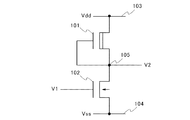
102 トランジスタ
103 電源線
104 電源線
105 ノード
106 トランジスタ
107 トランジスタ
108 容量素子
109 容量素子
110 ノード
111 トランジスタ
113 トランジスタ
114 ノード
115 ノード
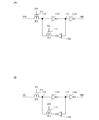
201 トランジスタ
202 トランジスタ
210 基板
212 ゲート絶縁層
215 電極
216 電極
217 電極
218 還元防止層
250 酸素空孔制御領域
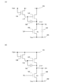
321 トランジスタ
322 トランジスタ
323 トランジスタ
324 電源線
325 電源線
326 ノード
580 基板
581 TFT
583 絶縁層
584 絶縁層
585 絶縁層
587 電極
588 電極
589 球形粒子
594 キャビティ
595 充填剤
596 基板
701 画素部
702 走査線駆動回路
703 信号線駆動回路
704 画素
804 走査線
805 信号線
821 トランジスタ
822 液晶素子
823 保持容量素子
851 トランジスタ
852 保持容量素子
853 トランジスタ
854 発光素子
855 走査線
856 信号線
900 シフトレジスタ
901 レベルシフタ
902 バッファ
903 シフトレジスタ
904 ラッチ回路
905 ラッチ回路
906 レベルシフタ
907 バッファ
1111 ノード
1121 インバータ
1122 インバータ
1123 インバータ
2000 基板
2001 ゲート電極
2002 ゲート絶縁層
2003 酸化物半導体層
2004a 酸化物半導体層
2004b 酸化物半導体層
2005a 電極
2005b 電極
2007 保護絶縁層
2008 電極
2020 電極
2022 電極
2023 電極
2024 電極
2028 電極
2029 電極
2050 端子
2051 端子
2052 ゲート絶縁層
2053 接続電極
2054 保護絶縁膜
2055 透明導電膜
2056 電極
2111 ゲート電極
2112 ゲート電極
2131 酸化物半導体層
2132 酸化物半導体層
2141a 酸化物半導体層
2141b 酸化物半導体層
2142a 酸化物半導体層
2142b 酸化物半導体層
2191 バッファ層
2192 バッファ層
2700 電子書籍
2701 筐体
2703 筐体
2705 表示部
2707 表示部
2711 軸部
2721 電源
2723 操作キー
2725 スピーカ
3011 論理回路
3012 論理回路
3013 論理回路
3111 トランジスタ
3112 トランジスタ
3113 トランジスタ
3121A インバータ
3121B インバータ
3121C インバータ
3122A インバータ
3122B インバータ
3122C インバータ
3123A インバータ
3123B インバータ
3123C インバータ
3131 トランジスタ
3132 トランジスタ
3133 トランジスタ
3140 NAND回路
3141 NAND回路
3142 NAND回路
3143 NAND回路
3171 ノード
3172 ノード
3173 ノード
4001 基板
4002 画素部
4003 信号線駆動回路
4004 走査線駆動回路
4005 シール材
4006 基板
4008 液晶層
4010 TFT
4011 TFT
4013 液晶素子
4015 接続端子電極
4016 端子電極
4018 FPC
4019 異方性導電膜
4020 絶縁層
4021 絶縁層
4030 画素電極
4031 対向電極
4032 絶縁層
4035 スペーサ
4501 基板
4502 画素部
4503a 信号線駆動回路
4504a 走査線駆動回路
4505 シール材
4506 基板
4507 充填材
4509 TFT
4510 TFT
4511 発光素子
4512 電界発光層
4513 電極
4515 接続端子電極
4516 端子電極
4517 電極
4518a FPC
4519 異方性導電膜
4520 隔壁
5001 基板
5002 ゲート電極
5003 ゲート絶縁層
5004 酸化物半導体層
5005a 電極
5005b 電極
5006 曲線
5007 曲線
590a 黒色領域
590b 白色領域
7001 TFT
7002 発光素子
7003 陰極
7004 発光層
7005 陽極
7011 駆動用TFT
7012 発光素子
7013 導電膜
7014 発光層
7015 陽極
7016 遮蔽膜
7017 陰極
7021 駆動用TFT
7022 発光素子
7023 導電膜
7024 発光層
7025 陽極
7027 陰極
9000 携帯電話機
9001 筐体
9002 表示部
9003 操作ボタン
9004 外部接続ポート
9005 スピーカ
9006 マイク
9400 通信装置
9401 筐体
9402 操作ボタン
9403 外部入力端子
9404 マイク
9405 スピーカ
9406 発光部
9410 表示装置
9411 筐体
9412 表示部
9413 操作ボタン
9600 テレビジョン装置
9601 筐体
9603 表示部
9605 スタンド
9607 表示部
9609 操作キー
9610 リモコン操作機
9700 デジタルフォトフレーム
9701 筐体
9703 表示部
9881 筐体
9882 表示部
9883 表示部
9884 スピーカ部
9885 入力手段(操作キー
9886 記録媒体挿入部
9887 接続端子
9888 センサ
9889 マイクロフォン
9890 LEDランプ
9891 筐体
9893 連結部
9900 スロットマシン
9901 筐体
9903 表示部
Claims (12)
- デプレッション型トランジスタと、
エンハンスメント型トランジスタと、を有し、
前記デプレッション型トランジスタのソース及びドレインの一方に、高電源電圧が与えられ、
前記デプレッション型トランジスタのゲートは、前記デプレッション型トランジスタのソース及びドレインの他方と電気的に接続され、
前記エンハンスメント型トランジスタのゲートに、第1の信号が入力され、
前記エンハンスメント型トランジスタのソース及びドレインの一方は、前記デプレッション型トランジスタのソース及びドレインの他方と電気的に接続され、
前記エンハンスメント型トランジスタのソース及びドレインの他方に、低電源電圧が与えられ、
前記デプレッション型トランジスタと前記エンハンスメント型トランジスタの接続箇所の電圧が、第2の信号として出力され、
前記デプレッション型トランジスタ及び前記エンハンスメント型トランジスタは、
ゲート電極と、
前記ゲート電極上に設けられたゲート絶縁層と、
前記ゲート絶縁層上に設けられた第1の酸化物半導体層と、
前記第1の酸化物半導体層の一部に接する一対の第2の酸化物半導体層と、
前記一対の第2の酸化物半導体層の一方に接するソース電極と、
前記一対の第2の酸化物半導体層の他方に接するドレイン電極と、を有し、
前記エンハンスメント型トランジスタは、前記第1の酸化物半導体層上で且つ前記ソース電極及び前記ドレイン電極の間の領域に還元防止層を有し、
前記デプレッション型トランジスタは、前記第1の酸化物半導体層上で且つ前記ソース電極及び前記ドレイン電極の間の領域に前記還元防止層を有さず、
前記エンハンスメント型トランジスタは、前記第1の酸化物半導体層における前記ゲート絶縁層との接触面と反対側の面であって前記ソース電極及び前記ドレイン電極の間に、酸素イオン照射処理によって形成された酸素空孔制御領域を有し、
前記酸素空孔制御領域は、前記デプレッション型トランジスタより、酸素空孔密度が低いことを特徴とする論理回路。 - 請求項1において、
前記一対の第2の酸化物半導体層は、ソース領域及びドレイン領域としての機能を有することを特徴とする論理回路。 - 請求項1または請求項2において、
前記第1の酸化物半導体層または前記第2の酸化物半導体層の少なくとも一方は、インジウム、ガリウム、及び亜鉛を有することを特徴とする論理回路。 - デプレッション型トランジスタと、
エンハンスメント型トランジスタと、を有し、
前記デプレッション型トランジスタのソース及びドレインの一方に、高電源電圧が与えられ、
前記デプレッション型トランジスタのゲートは、前記デプレッション型トランジスタのソース及びドレインの他方と電気的に接続され、
前記エンハンスメント型トランジスタのゲートに、第1の信号が入力され、
前記エンハンスメント型トランジスタのソース及びドレインの一方は、前記デプレッション型トランジスタのソース及びドレインの他方と電気的に接続され、
前記エンハンスメント型トランジスタのソース及びドレインの他方に、低電源電圧が与えられ、
前記デプレッション型トランジスタと前記エンハンスメント型トランジスタの接続箇所の電圧が、第2の信号として出力され、
前記デプレッション型トランジスタ及び前記エンハンスメント型トランジスタは、
ゲート電極と、
前記ゲート電極上に設けられたゲート絶縁層と、
前記ゲート絶縁層上に設けられた酸化物半導体層と、
前記酸化物半導体層の一部に接するソース電極及びドレイン電極と、を有し、
前記エンハンスメント型トランジスタは、前記酸化物半導体層上で且つ前記ソース電極及び前記ドレイン電極の間の領域に還元防止層を有し、
前記デプレッション型トランジスタは、前記酸化物半導体層上で且つ前記ソース電極及び前記ドレイン電極の間の領域に還元防止層を有さず、
前記エンハンスメント型トランジスタは、前記酸化物半導体層における前記ゲート絶縁層との接触面と反対側の面であって前記ソース電極及び前記ドレイン電極の間に、酸素イオン照射処理によって形成された酸素空孔制御領域を有し、
前記酸素空孔制御領域は、前記デプレッション型トランジスタより、酸素空孔密度が低いことを特徴とする論理回路。 - 請求項4において、
前記酸化物半導体層は、インジウム、ガリウム、及び亜鉛を有することを特徴とする論理回路。 - 請求項1乃至請求項5のいずれか一項において、
前記デプレッション型トランジスタ及び前記エンハンスメント型トランジスタを有する第1のインバータ回路並びに第2のインバータ回路と、
第3のインバータ回路と、
第1のトランジスタと、
第2のトランジスタと、を有し、
前記第1のトランジスタのゲートに、第1のクロック信号が入力され、
前記第1のトランジスタのソース及びドレインの一方に、入力信号が入力され、
前記第1のトランジスタのソース及びドレインの他方は、前記第1のインバータ回路の入力端子と電気的に接続され、
前記第1のインバータ回路の出力端子は、前記第2のインバータ回路の入力端子と電気的に接続され、
前記第1のインバータ回路の出力端子は、前記第3のインバータ回路の入力端子と電気的に接続され、
前記第3のインバータ回路の出力端子から出力信号が出力され、
前記第2のトランジスタのゲートに、第2のクロック信号が入力され、
前記第2のトランジスタのソース及びドレインの一方は、前記第1のトランジスタのソース及びドレインの他方と電気的に接続され、
前記第2のトランジスタのソース及びドレインの他方は、前記第2のインバータ回路の出力端子と電気的に接続されることを特徴とする論理回路。 - 請求項1乃至請求項6のいずれか一項において、
前記デプレッション型トランジスタ及び前記エンハンスメント型トランジスタは、同じ導電型を有することを特徴とする論理回路。 - 請求項1乃至請求項7のいずれか一項において、
前記エンハンスメント型トランジスタの前記ソース電極または前記ドレイン電極は、前記ゲート絶縁層に設けられた開口部を介して前記デプレッション型トランジスタのゲート電極に接することを特徴とする論理回路。 - 請求項1乃至請求項8のいずれか一項に記載の論理回路を用いることを特徴とする表示装置。
- 請求項9に記載の表示装置は、発光表示装置、液晶表示装置、または電気泳動表示装置としての機能を有することを特徴とする表示装置。
- 請求項1乃至請求項8のいずれか一項に記載の論理回路を有することを特徴とする電子機器。
- 請求項11に記載の電子機器は、テレビジョン装置、モニタ、カメラ、デジタルフォトフレーム、携帯電話機、携帯型ゲーム機、携帯情報端末、音響再生装置、または大型ゲーム機としての機能を有することを特徴とする電子機器。
Priority Applications (1)
| Application Number | Priority Date | Filing Date | Title |
|---|---|---|---|
| JP2009244086A JP5426318B2 (ja) | 2008-10-31 | 2009-10-23 | 論理回路 |
Applications Claiming Priority (3)
| Application Number | Priority Date | Filing Date | Title |
|---|---|---|---|
| JP2008281647 | 2008-10-31 | ||
| JP2008281647 | 2008-10-31 | ||
| JP2009244086A JP5426318B2 (ja) | 2008-10-31 | 2009-10-23 | 論理回路 |
Related Child Applications (1)
| Application Number | Title | Priority Date | Filing Date |
|---|---|---|---|
| JP2013246499A Division JP5732123B2 (ja) | 2008-10-31 | 2013-11-28 | 半導体装置 |
Publications (3)
| Publication Number | Publication Date |
|---|---|
| JP2010135760A JP2010135760A (ja) | 2010-06-17 |
| JP2010135760A5 JP2010135760A5 (ja) | 2012-02-09 |
| JP5426318B2 true JP5426318B2 (ja) | 2014-02-26 |
Family
ID=42130624
Family Applications (3)
| Application Number | Title | Priority Date | Filing Date |
|---|---|---|---|
| JP2009244086A Expired - Fee Related JP5426318B2 (ja) | 2008-10-31 | 2009-10-23 | 論理回路 |
| JP2013246499A Active JP5732123B2 (ja) | 2008-10-31 | 2013-11-28 | 半導体装置 |
| JP2015079968A Active JP6246156B2 (ja) | 2008-10-31 | 2015-04-09 | 半導体装置及び半導体装置の作製方法 |
Family Applications After (2)
| Application Number | Title | Priority Date | Filing Date |
|---|---|---|---|
| JP2013246499A Active JP5732123B2 (ja) | 2008-10-31 | 2013-11-28 | 半導体装置 |
| JP2015079968A Active JP6246156B2 (ja) | 2008-10-31 | 2015-04-09 | 半導体装置及び半導体装置の作製方法 |
Country Status (5)
| Country | Link |
|---|---|
| US (3) | US7952392B2 (ja) |
| JP (3) | JP5426318B2 (ja) |
| KR (2) | KR101631454B1 (ja) |
| CN (1) | CN101728383B (ja) |
| TW (2) | TWI550827B (ja) |
Cited By (1)
| Publication number | Priority date | Publication date | Assignee | Title |
|---|---|---|---|---|
| KR101863366B1 (ko) | 2010-07-30 | 2018-05-31 | 소니 세미컨덕터 솔루션즈 가부시키가이샤 | 고체 촬상 장치 및 그 구동 방법 및 전자 기기 |
Families Citing this family (67)
| Publication number | Priority date | Publication date | Assignee | Title |
|---|---|---|---|---|
| CN102197490B (zh) | 2008-10-24 | 2013-11-06 | 株式会社半导体能源研究所 | 半导体器件和用于制造该半导体器件的方法 |
| US8106400B2 (en) | 2008-10-24 | 2012-01-31 | Semiconductor Energy Laboratory Co., Ltd. | Semiconductor device and method for manufacturing the same |
| JP5590868B2 (ja) * | 2008-12-11 | 2014-09-17 | 株式会社半導体エネルギー研究所 | 半導体装置 |
| WO2011027661A1 (en) | 2009-09-04 | 2011-03-10 | Semiconductor Energy Laboratory Co., Ltd. | Light-emitting device and method for manufacturing the same |
| WO2011034012A1 (en) * | 2009-09-16 | 2011-03-24 | Semiconductor Energy Laboratory Co., Ltd. | Logic circuit, light emitting device, semiconductor device, and electronic device |
| KR20170024130A (ko) * | 2009-10-21 | 2017-03-06 | 가부시키가이샤 한도오따이 에네루기 켄큐쇼 | 반도체 장치 및 그 제조 방법 |
| KR101750982B1 (ko) | 2009-11-06 | 2017-06-26 | 가부시키가이샤 한도오따이 에네루기 켄큐쇼 | 반도체 장치 및 반도체 장치의 제작 방법 |
| JP5581677B2 (ja) * | 2009-12-04 | 2014-09-03 | セイコーエプソン株式会社 | 電気泳動表示装置及び電子機器 |
| WO2011070929A1 (en) | 2009-12-11 | 2011-06-16 | Semiconductor Energy Laboratory Co., Ltd. | Semiconductor device and electronic device |
| WO2011074407A1 (en) * | 2009-12-18 | 2011-06-23 | Semiconductor Energy Laboratory Co., Ltd. | Semiconductor device and method for manufacturing the same |
| CN102822884A (zh) * | 2010-03-26 | 2012-12-12 | 夏普株式会社 | 显示装置和显示装置用阵列基板的制造方法 |
| JP5714973B2 (ja) | 2010-05-21 | 2015-05-07 | 株式会社半導体エネルギー研究所 | 半導体装置 |
| US8610180B2 (en) * | 2010-06-11 | 2013-12-17 | Semiconductor Energy Laboratory Co., Ltd. | Gas sensor and method for manufacturing the gas sensor |
| WO2012002236A1 (en) | 2010-06-29 | 2012-01-05 | Semiconductor Energy Laboratory Co., Ltd. | Wiring board, semiconductor device, and manufacturing methods thereof |
| US8785241B2 (en) * | 2010-07-16 | 2014-07-22 | Semiconductor Energy Laboratory Co., Ltd. | Semiconductor device and manufacturing method thereof |
| CN103069717B (zh) | 2010-08-06 | 2018-01-30 | 株式会社半导体能源研究所 | 半导体集成电路 |
| WO2012029612A1 (en) * | 2010-09-03 | 2012-03-08 | Semiconductor Energy Laboratory Co., Ltd. | Sputtering target and method for manufacturing semiconductor device |
| US8766253B2 (en) * | 2010-09-10 | 2014-07-01 | Semiconductor Energy Laboratory Co., Ltd. | Semiconductor device |
| TWI624878B (zh) | 2011-03-11 | 2018-05-21 | 半導體能源研究所股份有限公司 | 半導體裝置的製造方法 |
| TWI568181B (zh) * | 2011-05-06 | 2017-01-21 | 半導體能源研究所股份有限公司 | 邏輯電路及半導體裝置 |
| US8581625B2 (en) | 2011-05-19 | 2013-11-12 | Semiconductor Energy Laboratory Co., Ltd. | Programmable logic device |
| KR101922397B1 (ko) * | 2011-05-20 | 2018-11-28 | 가부시키가이샤 한도오따이 에네루기 켄큐쇼 | 반도체 장치 |
| TWI616873B (zh) * | 2011-05-20 | 2018-03-01 | 半導體能源研究所股份有限公司 | 儲存裝置及信號處理電路 |
| TWI559683B (zh) * | 2011-05-20 | 2016-11-21 | 半導體能源研究所股份有限公司 | 半導體積體電路 |
| JP2013084333A (ja) | 2011-09-28 | 2013-05-09 | Semiconductor Energy Lab Co Ltd | シフトレジスタ回路 |
| TWI497689B (zh) * | 2011-12-02 | 2015-08-21 | Ind Tech Res Inst | 半導體元件及其製造方法 |
| TWI470809B (zh) * | 2011-12-29 | 2015-01-21 | E Ink Holdings Inc | 薄膜電晶體陣列基板及其製造方法與使用在其製造方法之退火爐 |
| CN102636678B (zh) * | 2012-04-10 | 2015-01-21 | 北京大学 | 阈值电压退化测量电路 |
| CN103474467B (zh) | 2012-06-05 | 2016-04-13 | 元太科技工业股份有限公司 | 薄膜晶体管结构及其阵列基板 |
| US8933461B2 (en) * | 2012-08-09 | 2015-01-13 | Texas Instruments Incorporated | III-nitride enhancement mode transistors with tunable and high gate-source voltage rating |
| JPWO2014034346A1 (ja) * | 2012-08-28 | 2016-08-08 | シャープ株式会社 | 複合型半導体装置 |
| US20150214374A1 (en) * | 2012-08-30 | 2015-07-30 | Sharp Kabushiki Kaisha | Circuit board and display device |
| KR102042483B1 (ko) * | 2012-09-24 | 2019-11-12 | 한국전자통신연구원 | 박막 트랜지스터 및 그 제조 방법 |
| WO2014054563A1 (ja) * | 2012-10-03 | 2014-04-10 | シャープ株式会社 | 半導体装置及び表示装置 |
| EP2768141A1 (en) | 2013-02-15 | 2014-08-20 | Technische Universität Darmstadt | Active loads, especially for use in inverter circuits |
| DE102014208859B4 (de) * | 2013-05-20 | 2021-03-11 | Semiconductor Energy Laboratory Co., Ltd. | Halbleitervorrichtung |
| KR102050447B1 (ko) * | 2013-06-28 | 2019-12-02 | 엘지디스플레이 주식회사 | 인버터, 그를 가지는 액정 표시 장치 및 그 액정 표시 장치의 제조 방법 |
| CN103412449B (zh) * | 2013-07-23 | 2015-11-18 | 合肥京东方光电科技有限公司 | 一种阵列基板及其制作方法、显示装置 |
| KR102169861B1 (ko) * | 2013-11-07 | 2020-10-26 | 엘지디스플레이 주식회사 | 어레이기판 및 이의 제조방법 |
| KR101536174B1 (ko) * | 2014-02-11 | 2015-07-14 | 연세대학교 산학협력단 | 산소 확산을 억제할 수 있는 반도체 소자 제조 방법 |
| KR102354008B1 (ko) * | 2014-05-29 | 2022-01-24 | 가부시키가이샤 한도오따이 에네루기 켄큐쇼 | 반도체 장치, 반도체 장치의 제작 방법 및 전자 기기 |
| JP2016029719A (ja) * | 2014-07-17 | 2016-03-03 | 出光興産株式会社 | 薄膜トランジスタ |
| TWI691088B (zh) | 2014-11-21 | 2020-04-11 | 日商半導體能源研究所股份有限公司 | 半導體裝置 |
| US9852248B2 (en) * | 2014-12-22 | 2017-12-26 | Wallace W Lin | Transistor plasma charging eliminator |
| US9996654B2 (en) * | 2014-12-22 | 2018-06-12 | Wallace W Lin | Transistor plasma charging evaluator |
| CN104575425B (zh) * | 2015-01-09 | 2017-04-12 | 深圳市华星光电技术有限公司 | 扫描驱动电路及其与非门逻辑运算电路 |
| FI20150334A (fi) | 2015-01-14 | 2016-07-15 | Artto Mikael Aurola | Paranneltu puolijohdekokoonpano |
| WO2016113468A1 (en) * | 2015-01-14 | 2016-07-21 | Aurola Artto Mikael | A semiconductor logic element and a logic circuitry |
| US9633710B2 (en) | 2015-01-23 | 2017-04-25 | Semiconductor Energy Laboratory Co., Ltd. | Method for operating semiconductor device |
| TWI691512B (zh) | 2015-02-20 | 2020-04-21 | 日商橘生藥品工業股份有限公司 | Fc融合高親和性IgE受體α鏈 |
| RU2613853C2 (ru) * | 2015-03-04 | 2017-03-21 | Федеральное государственное бюджетное учреждение науки Институт проблем управления им. В.А. Трапезникова Российской академии наук | Многовходовый логический элемент И |
| KR101596377B1 (ko) * | 2015-04-08 | 2016-02-22 | 실리콘 디스플레이 (주) | 정전용량 지문센서 |
| CN105140271B (zh) * | 2015-07-16 | 2019-03-26 | 深圳市华星光电技术有限公司 | 薄膜晶体管、薄膜晶体管的制造方法及显示装置 |
| US9935127B2 (en) * | 2015-07-29 | 2018-04-03 | Wuhan China Star Optoelectronics Technology Co., Ltd. | Control circuit of thin film transistor |
| SG10201607278TA (en) * | 2015-09-18 | 2017-04-27 | Semiconductor Energy Lab Co Ltd | Semiconductor device and electronic device |
| WO2017064590A1 (en) * | 2015-10-12 | 2017-04-20 | Semiconductor Energy Laboratory Co., Ltd. | Method for manufacturing semiconductor device |
| US10043917B2 (en) | 2016-03-03 | 2018-08-07 | United Microelectronics Corp. | Oxide semiconductor device and method of manufacturing the same |
| FI20160183L (fi) * | 2016-07-14 | 2016-07-15 | Artto Mikael Aurola | Parannettu puolijohdekokoonpano |
| WO2019066872A1 (en) * | 2017-09-28 | 2019-04-04 | Intel Corporation | MONOLITHIC INTEGRATION OF A THIN FILM TRANSISTOR ON A COMPLEMENTARY TRANSISTOR |
| EP3588780B1 (en) * | 2018-06-28 | 2021-03-03 | IMEC vzw | Low power logic circuit |
| US10700683B1 (en) * | 2018-08-28 | 2020-06-30 | Qualcomm Incorporated | Dynamic power supply shifting |
| KR102130322B1 (ko) * | 2019-01-03 | 2020-07-06 | 청주대학교 산학협력단 | 박막 트랜지스터 논리회로 및 그 제조방법 |
| US11379231B2 (en) | 2019-10-25 | 2022-07-05 | Semiconductor Energy Laboratory Co., Ltd. | Data processing system and operation method of data processing system |
| US11127719B2 (en) | 2020-01-23 | 2021-09-21 | Nvidia Corporation | Face-to-face dies with enhanced power delivery using extended TSVS |
| US11699662B2 (en) * | 2020-01-23 | 2023-07-11 | Nvidia Corporation | Face-to-face dies with probe pads for pre-assembly testing |
| US11616023B2 (en) | 2020-01-23 | 2023-03-28 | Nvidia Corporation | Face-to-face dies with a void for enhanced inductor performance |
| CN112290931A (zh) * | 2020-12-07 | 2021-01-29 | 南京元络芯科技有限公司 | 基于化合物半导体的逻辑控制电路 |
Family Cites Families (140)
| Publication number | Priority date | Publication date | Assignee | Title |
|---|---|---|---|---|
| US757966A (en) * | 1903-02-28 | 1904-04-19 | John Madden | Machine for sewing corsets. |
| JPS60198861A (ja) | 1984-03-23 | 1985-10-08 | Fujitsu Ltd | 薄膜トランジスタ |
| US4615102A (en) * | 1984-05-01 | 1986-10-07 | Fujitsu Limited | Method of producing enhancement mode and depletion mode FETs |
| JPH0244256B2 (ja) | 1987-01-28 | 1990-10-03 | Kagaku Gijutsucho Mukizaishitsu Kenkyushocho | Ingazn2o5deshimesarerurotsuhoshokeinosojokozoojusurukagobutsuoyobisonoseizoho |
| JPH0244258B2 (ja) | 1987-02-24 | 1990-10-03 | Kagaku Gijutsucho Mukizaishitsu Kenkyushocho | Ingazn3o6deshimesarerurotsuhoshokeinosojokozoojusurukagobutsuoyobisonoseizoho |
| JPS63210023A (ja) | 1987-02-24 | 1988-08-31 | Natl Inst For Res In Inorg Mater | InGaZn↓4O↓7で示される六方晶系の層状構造を有する化合物およびその製造法 |
| JPH0244260B2 (ja) | 1987-02-24 | 1990-10-03 | Kagaku Gijutsucho Mukizaishitsu Kenkyushocho | Ingazn5o8deshimesarerurotsuhoshokeinosojokozoojusurukagobutsuoyobisonoseizoho |
| JPH0244262B2 (ja) | 1987-02-27 | 1990-10-03 | Kagaku Gijutsucho Mukizaishitsu Kenkyushocho | Ingazn6o9deshimesarerurotsuhoshokeinosojokozoojusurukagobutsuoyobisonoseizoho |
| JPH0244263B2 (ja) | 1987-04-22 | 1990-10-03 | Kagaku Gijutsucho Mukizaishitsu Kenkyushocho | Ingazn7o10deshimesarerurotsuhoshokeinosojokozoojusurukagobutsuoyobisonoseizoho |
| EP0445535B1 (en) | 1990-02-06 | 1995-02-01 | Sel Semiconductor Energy Laboratory Co., Ltd. | Method of forming an oxide film |
| JP2585118B2 (ja) | 1990-02-06 | 1997-02-26 | 株式会社半導体エネルギー研究所 | 薄膜トランジスタの作製方法 |
| JP3057787B2 (ja) * | 1991-03-13 | 2000-07-04 | 日本電気株式会社 | Lsiのテスト回路 |
| JPH05251705A (ja) | 1992-03-04 | 1993-09-28 | Fuji Xerox Co Ltd | 薄膜トランジスタ |
| JP3479375B2 (ja) | 1995-03-27 | 2003-12-15 | 科学技術振興事業団 | 亜酸化銅等の金属酸化物半導体による薄膜トランジスタとpn接合を形成した金属酸化物半導体装置およびそれらの製造方法 |
| DE69635107D1 (de) | 1995-08-03 | 2005-09-29 | Koninkl Philips Electronics Nv | Halbleiteranordnung mit einem transparenten schaltungselement |
| GB9520888D0 (en) * | 1995-10-12 | 1995-12-13 | Philips Electronics Nv | Electronic devices comprising thin-film circuitry |
| US5847410A (en) | 1995-11-24 | 1998-12-08 | Semiconductor Energy Laboratory Co. | Semiconductor electro-optical device |
| JP3625598B2 (ja) | 1995-12-30 | 2005-03-02 | 三星電子株式会社 | 液晶表示装置の製造方法 |
| JP4170454B2 (ja) | 1998-07-24 | 2008-10-22 | Hoya株式会社 | 透明導電性酸化物薄膜を有する物品及びその製造方法 |
| JP2000150861A (ja) | 1998-11-16 | 2000-05-30 | Tdk Corp | 酸化物薄膜 |
| JP3276930B2 (ja) | 1998-11-17 | 2002-04-22 | 科学技術振興事業団 | トランジスタ及び半導体装置 |
| TW460731B (en) | 1999-09-03 | 2001-10-21 | Ind Tech Res Inst | Electrode structure and production method of wide viewing angle LCD |
| US7633471B2 (en) * | 2000-05-12 | 2009-12-15 | Semiconductor Energy Laboratory Co., Ltd. | Light-emitting device and electric appliance |
| JP4089858B2 (ja) | 2000-09-01 | 2008-05-28 | 国立大学法人東北大学 | 半導体デバイス |
| KR20020038482A (ko) * | 2000-11-15 | 2002-05-23 | 모리시타 요이찌 | 박막 트랜지스터 어레이, 그 제조방법 및 그것을 이용한표시패널 |
| JP4115841B2 (ja) * | 2001-03-16 | 2008-07-09 | ノバルティス アクチエンゲゼルシャフト | 眼科用レンズを注型成形するための型及び方法 |
| JP3997731B2 (ja) * | 2001-03-19 | 2007-10-24 | 富士ゼロックス株式会社 | 基材上に結晶性半導体薄膜を形成する方法 |
| JP2002289859A (ja) | 2001-03-23 | 2002-10-04 | Minolta Co Ltd | 薄膜トランジスタ |
| JP3925839B2 (ja) | 2001-09-10 | 2007-06-06 | シャープ株式会社 | 半導体記憶装置およびその試験方法 |
| JP4090716B2 (ja) | 2001-09-10 | 2008-05-28 | 雅司 川崎 | 薄膜トランジスタおよびマトリクス表示装置 |
| US7061014B2 (en) | 2001-11-05 | 2006-06-13 | Japan Science And Technology Agency | Natural-superlattice homologous single crystal thin film, method for preparation thereof, and device using said single crystal thin film |
| JP4164562B2 (ja) | 2002-09-11 | 2008-10-15 | 独立行政法人科学技術振興機構 | ホモロガス薄膜を活性層として用いる透明薄膜電界効果型トランジスタ |
| JP4083486B2 (ja) | 2002-02-21 | 2008-04-30 | 独立行政法人科学技術振興機構 | LnCuO(S,Se,Te)単結晶薄膜の製造方法 |
| CN1445821A (zh) | 2002-03-15 | 2003-10-01 | 三洋电机株式会社 | ZnO膜和ZnO半导体层的形成方法、半导体元件及其制造方法 |
| JP3933591B2 (ja) | 2002-03-26 | 2007-06-20 | 淳二 城戸 | 有機エレクトロルミネッセント素子 |
| US7339187B2 (en) * | 2002-05-21 | 2008-03-04 | State Of Oregon Acting By And Through The Oregon State Board Of Higher Education On Behalf Of Oregon State University | Transistor structures |
| JP2004022625A (ja) | 2002-06-13 | 2004-01-22 | Murata Mfg Co Ltd | 半導体デバイス及び該半導体デバイスの製造方法 |
| US7105868B2 (en) | 2002-06-24 | 2006-09-12 | Cermet, Inc. | High-electron mobility transistor with zinc oxide |
| US7067843B2 (en) | 2002-10-11 | 2006-06-27 | E. I. Du Pont De Nemours And Company | Transparent oxide semiconductor thin film transistors |
| US6788567B2 (en) * | 2002-12-02 | 2004-09-07 | Rohm Co., Ltd. | Data holding device and data holding method |
| JP2004235180A (ja) * | 2003-01-28 | 2004-08-19 | Sanyo Electric Co Ltd | 半導体装置及びその製造方法 |
| JP4166105B2 (ja) | 2003-03-06 | 2008-10-15 | シャープ株式会社 | 半導体装置およびその製造方法 |
| JP2004273732A (ja) | 2003-03-07 | 2004-09-30 | Sharp Corp | アクティブマトリクス基板およびその製造方法 |
| JP4108633B2 (ja) | 2003-06-20 | 2008-06-25 | シャープ株式会社 | 薄膜トランジスタおよびその製造方法ならびに電子デバイス |
| US7262463B2 (en) | 2003-07-25 | 2007-08-28 | Hewlett-Packard Development Company, L.P. | Transistor including a deposited channel region having a doped portion |
| JP2005191821A (ja) * | 2003-12-25 | 2005-07-14 | Seiko Epson Corp | コンパレータ回路及び電源回路 |
| WO2005088726A1 (ja) | 2004-03-12 | 2005-09-22 | Japan Science And Technology Agency | アモルファス酸化物及び薄膜トランジスタ |
| US7297977B2 (en) | 2004-03-12 | 2007-11-20 | Hewlett-Packard Development Company, L.P. | Semiconductor device |
| US7145174B2 (en) | 2004-03-12 | 2006-12-05 | Hewlett-Packard Development Company, Lp. | Semiconductor device |
| US7282782B2 (en) | 2004-03-12 | 2007-10-16 | Hewlett-Packard Development Company, L.P. | Combined binary oxide semiconductor device |
| US7211825B2 (en) * | 2004-06-14 | 2007-05-01 | Yi-Chi Shih | Indium oxide-based thin film transistors and circuits |
| JP4286738B2 (ja) | 2004-07-14 | 2009-07-01 | 株式会社半導体エネルギー研究所 | 絶縁ゲイト型電界効果半導体装置の作製方法 |
| JP2006100760A (ja) * | 2004-09-02 | 2006-04-13 | Casio Comput Co Ltd | 薄膜トランジスタおよびその製造方法 |
| US7285501B2 (en) | 2004-09-17 | 2007-10-23 | Hewlett-Packard Development Company, L.P. | Method of forming a solution processed device |
| US7298084B2 (en) | 2004-11-02 | 2007-11-20 | 3M Innovative Properties Company | Methods and displays utilizing integrated zinc oxide row and column drivers in conjunction with organic light emitting diodes |
| BRPI0517560B8 (pt) | 2004-11-10 | 2018-12-11 | Canon Kk | transistor de efeito de campo |
| JP5053537B2 (ja) * | 2004-11-10 | 2012-10-17 | キヤノン株式会社 | 非晶質酸化物を利用した半導体デバイス |
| RU2358354C2 (ru) | 2004-11-10 | 2009-06-10 | Кэнон Кабусики Кайся | Светоизлучающее устройство |
| US7791072B2 (en) | 2004-11-10 | 2010-09-07 | Canon Kabushiki Kaisha | Display |
| CA2585190A1 (en) | 2004-11-10 | 2006-05-18 | Canon Kabushiki Kaisha | Amorphous oxide and field effect transistor |
| US7829444B2 (en) | 2004-11-10 | 2010-11-09 | Canon Kabushiki Kaisha | Field effect transistor manufacturing method |
| JP5126730B2 (ja) * | 2004-11-10 | 2013-01-23 | キヤノン株式会社 | 電界効果型トランジスタの製造方法 |
| US7453065B2 (en) | 2004-11-10 | 2008-11-18 | Canon Kabushiki Kaisha | Sensor and image pickup device |
| US7863611B2 (en) | 2004-11-10 | 2011-01-04 | Canon Kabushiki Kaisha | Integrated circuits utilizing amorphous oxides |
| US8003449B2 (en) * | 2004-11-26 | 2011-08-23 | Semiconductor Energy Laboratory Co., Ltd. | Method of manufacturing a semiconductor device having a reverse staggered thin film transistor |
| EP1834360A2 (en) | 2004-12-30 | 2007-09-19 | Koninklijke Philips Electronics N.V. | Enhancement - depletion semiconductor structure and method for making it |
| US7579224B2 (en) | 2005-01-21 | 2009-08-25 | Semiconductor Energy Laboratory Co., Ltd. | Method for manufacturing a thin film semiconductor device |
| TWI390735B (zh) | 2005-01-28 | 2013-03-21 | Semiconductor Energy Lab | 半導體裝置,電子裝置,和半導體裝置的製造方法 |
| TWI505473B (zh) | 2005-01-28 | 2015-10-21 | Semiconductor Energy Lab | 半導體裝置,電子裝置,和半導體裝置的製造方法 |
| US7858451B2 (en) | 2005-02-03 | 2010-12-28 | Semiconductor Energy Laboratory Co., Ltd. | Electronic device, semiconductor device and manufacturing method thereof |
| US7492028B2 (en) * | 2005-02-18 | 2009-02-17 | Semiconductor Energy Laboratory Co., Ltd. | Photoelectric conversion device and manufacturing method of the same, and a semiconductor device |
| US7948171B2 (en) | 2005-02-18 | 2011-05-24 | Semiconductor Energy Laboratory Co., Ltd. | Light emitting device |
| US20060197092A1 (en) | 2005-03-03 | 2006-09-07 | Randy Hoffman | System and method for forming conductive material on a substrate |
| US8681077B2 (en) | 2005-03-18 | 2014-03-25 | Semiconductor Energy Laboratory Co., Ltd. | Semiconductor device, and display device, driving method and electronic apparatus thereof |
| WO2006105077A2 (en) | 2005-03-28 | 2006-10-05 | Massachusetts Institute Of Technology | Low voltage thin film transistor with high-k dielectric material |
| US7645478B2 (en) | 2005-03-31 | 2010-01-12 | 3M Innovative Properties Company | Methods of making displays |
| US8300031B2 (en) | 2005-04-20 | 2012-10-30 | Semiconductor Energy Laboratory Co., Ltd. | Semiconductor device comprising transistor having gate and drain connected through a current-voltage conversion element |
| JP2006344849A (ja) | 2005-06-10 | 2006-12-21 | Casio Comput Co Ltd | 薄膜トランジスタ |
| US7402506B2 (en) | 2005-06-16 | 2008-07-22 | Eastman Kodak Company | Methods of making thin film transistors comprising zinc-oxide-based semiconductor materials and transistors made thereby |
| US7691666B2 (en) | 2005-06-16 | 2010-04-06 | Eastman Kodak Company | Methods of making thin film transistors comprising zinc-oxide-based semiconductor materials and transistors made thereby |
| US7507618B2 (en) | 2005-06-27 | 2009-03-24 | 3M Innovative Properties Company | Method for making electronic devices using metal oxide nanoparticles |
| KR100711890B1 (ko) | 2005-07-28 | 2007-04-25 | 삼성에스디아이 주식회사 | 유기 발광표시장치 및 그의 제조방법 |
| JP2007059128A (ja) | 2005-08-23 | 2007-03-08 | Canon Inc | 有機el表示装置およびその製造方法 |
| JP4280736B2 (ja) | 2005-09-06 | 2009-06-17 | キヤノン株式会社 | 半導体素子 |
| JP2007073705A (ja) | 2005-09-06 | 2007-03-22 | Canon Inc | 酸化物半導体チャネル薄膜トランジスタおよびその製造方法 |
| JP4850457B2 (ja) | 2005-09-06 | 2012-01-11 | キヤノン株式会社 | 薄膜トランジスタ及び薄膜ダイオード |
| JP5116225B2 (ja) | 2005-09-06 | 2013-01-09 | キヤノン株式会社 | 酸化物半導体デバイスの製造方法 |
| EP1998373A3 (en) | 2005-09-29 | 2012-10-31 | Semiconductor Energy Laboratory Co, Ltd. | Semiconductor device having oxide semiconductor layer and manufacturing method thereof |
| JP5064747B2 (ja) | 2005-09-29 | 2012-10-31 | 株式会社半導体エネルギー研究所 | 半導体装置、電気泳動表示装置、表示モジュール、電子機器、及び半導体装置の作製方法 |
| JP5078246B2 (ja) | 2005-09-29 | 2012-11-21 | 株式会社半導体エネルギー研究所 | 半導体装置、及び半導体装置の作製方法 |
| JP5037808B2 (ja) | 2005-10-20 | 2012-10-03 | キヤノン株式会社 | アモルファス酸化物を用いた電界効果型トランジスタ、及び該トランジスタを用いた表示装置 |
| CN101667544B (zh) | 2005-11-15 | 2012-09-05 | 株式会社半导体能源研究所 | 半导体器件及其制造方法 |
| JP5250929B2 (ja) * | 2005-11-30 | 2013-07-31 | 凸版印刷株式会社 | トランジスタおよびその製造方法 |
| JP2007158105A (ja) * | 2005-12-06 | 2007-06-21 | Matsushita Electric Ind Co Ltd | 集積回路およびその製造方法 |
| US8212953B2 (en) * | 2005-12-26 | 2012-07-03 | Semiconductor Energy Laboratory Co., Ltd. | Semiconductor device and method for manufacturing the same |
| TWI292281B (en) | 2005-12-29 | 2008-01-01 | Ind Tech Res Inst | Pixel structure of active organic light emitting diode and method of fabricating the same |
| US7867636B2 (en) | 2006-01-11 | 2011-01-11 | Murata Manufacturing Co., Ltd. | Transparent conductive film and method for manufacturing the same |
| JP4977478B2 (ja) | 2006-01-21 | 2012-07-18 | 三星電子株式会社 | ZnOフィルム及びこれを用いたTFTの製造方法 |
| US7576394B2 (en) | 2006-02-02 | 2009-08-18 | Kochi Industrial Promotion Center | Thin film transistor including low resistance conductive thin films and manufacturing method thereof |
| US7977169B2 (en) | 2006-02-15 | 2011-07-12 | Kochi Industrial Promotion Center | Semiconductor device including active layer made of zinc oxide with controlled orientations and manufacturing method thereof |
| JP5110803B2 (ja) | 2006-03-17 | 2012-12-26 | キヤノン株式会社 | 酸化物膜をチャネルに用いた電界効果型トランジスタ及びその製造方法 |
| JP4761458B2 (ja) * | 2006-03-27 | 2011-08-31 | セイコーインスツル株式会社 | カスコード回路および半導体装置 |
| KR20070101595A (ko) | 2006-04-11 | 2007-10-17 | 삼성전자주식회사 | ZnO TFT |
| US20070252928A1 (en) | 2006-04-28 | 2007-11-01 | Toppan Printing Co., Ltd. | Structure, transmission type liquid crystal display, reflection type display and manufacturing method thereof |
| JP5135709B2 (ja) * | 2006-04-28 | 2013-02-06 | 凸版印刷株式会社 | 薄膜トランジスタ及びその製造方法 |
| KR100801961B1 (ko) | 2006-05-26 | 2008-02-12 | 한국전자통신연구원 | 듀얼 게이트 유기트랜지스터를 이용한 인버터 |
| JP5028033B2 (ja) | 2006-06-13 | 2012-09-19 | キヤノン株式会社 | 酸化物半導体膜のドライエッチング方法 |
| JP4609797B2 (ja) * | 2006-08-09 | 2011-01-12 | Nec液晶テクノロジー株式会社 | 薄膜デバイス及びその製造方法 |
| JP4999400B2 (ja) | 2006-08-09 | 2012-08-15 | キヤノン株式会社 | 酸化物半導体膜のドライエッチング方法 |
| JP5127183B2 (ja) * | 2006-08-23 | 2013-01-23 | キヤノン株式会社 | アモルファス酸化物半導体膜を用いた薄膜トランジスタの製造方法 |
| JP5128792B2 (ja) * | 2006-08-31 | 2013-01-23 | 財団法人高知県産業振興センター | 薄膜トランジスタの製法 |
| JP4332545B2 (ja) | 2006-09-15 | 2009-09-16 | キヤノン株式会社 | 電界効果型トランジスタ及びその製造方法 |
| JP5164357B2 (ja) | 2006-09-27 | 2013-03-21 | キヤノン株式会社 | 半導体装置及び半導体装置の製造方法 |
| JP4274219B2 (ja) | 2006-09-27 | 2009-06-03 | セイコーエプソン株式会社 | 電子デバイス、有機エレクトロルミネッセンス装置、有機薄膜半導体装置 |
| KR100790761B1 (ko) * | 2006-09-29 | 2008-01-03 | 한국전자통신연구원 | 인버터 |
| US7622371B2 (en) | 2006-10-10 | 2009-11-24 | Hewlett-Packard Development Company, L.P. | Fused nanocrystal thin film semiconductor and method |
| US7772021B2 (en) | 2006-11-29 | 2010-08-10 | Samsung Electronics Co., Ltd. | Flat panel displays comprising a thin-film transistor having a semiconductive oxide in its channel and methods of fabricating the same for use in flat panel displays |
| JP2008140684A (ja) | 2006-12-04 | 2008-06-19 | Toppan Printing Co Ltd | カラーelディスプレイおよびその製造方法 |
| JP5305630B2 (ja) * | 2006-12-05 | 2013-10-02 | キヤノン株式会社 | ボトムゲート型薄膜トランジスタの製造方法及び表示装置の製造方法 |
| KR101303578B1 (ko) | 2007-01-05 | 2013-09-09 | 삼성전자주식회사 | 박막 식각 방법 |
| US8207063B2 (en) | 2007-01-26 | 2012-06-26 | Eastman Kodak Company | Process for atomic layer deposition |
| JP5121254B2 (ja) | 2007-02-28 | 2013-01-16 | キヤノン株式会社 | 薄膜トランジスタおよび表示装置 |
| KR100858088B1 (ko) | 2007-02-28 | 2008-09-10 | 삼성전자주식회사 | 박막 트랜지스터 및 그 제조 방법 |
| KR100851215B1 (ko) | 2007-03-14 | 2008-08-07 | 삼성에스디아이 주식회사 | 박막 트랜지스터 및 이를 이용한 유기 전계 발광표시장치 |
| US8530891B2 (en) * | 2007-04-05 | 2013-09-10 | Idemitsu Kosan Co., Ltd | Field-effect transistor, and process for producing field-effect transistor |
| US7795613B2 (en) | 2007-04-17 | 2010-09-14 | Toppan Printing Co., Ltd. | Structure with transistor |
| KR101325053B1 (ko) | 2007-04-18 | 2013-11-05 | 삼성디스플레이 주식회사 | 박막 트랜지스터 기판 및 이의 제조 방법 |
| KR20080094300A (ko) | 2007-04-19 | 2008-10-23 | 삼성전자주식회사 | 박막 트랜지스터 및 그 제조 방법과 박막 트랜지스터를포함하는 평판 디스플레이 |
| KR101334181B1 (ko) | 2007-04-20 | 2013-11-28 | 삼성전자주식회사 | 선택적으로 결정화된 채널층을 갖는 박막 트랜지스터 및 그제조 방법 |
| CN101663762B (zh) * | 2007-04-25 | 2011-09-21 | 佳能株式会社 | 氧氮化物半导体 |
| JP5294651B2 (ja) | 2007-05-18 | 2013-09-18 | キヤノン株式会社 | インバータの作製方法及びインバータ |
| KR101345376B1 (ko) | 2007-05-29 | 2013-12-24 | 삼성전자주식회사 | ZnO 계 박막 트랜지스터 및 그 제조방법 |
| JP5215158B2 (ja) | 2007-12-17 | 2013-06-19 | 富士フイルム株式会社 | 無機結晶性配向膜及びその製造方法、半導体デバイス |
| KR101490112B1 (ko) | 2008-03-28 | 2015-02-05 | 삼성전자주식회사 | 인버터 및 그를 포함하는 논리회로 |
| TWI413260B (zh) | 2008-07-31 | 2013-10-21 | Semiconductor Energy Lab | 半導體裝置及其製造方法 |
| JP4623179B2 (ja) * | 2008-09-18 | 2011-02-02 | ソニー株式会社 | 薄膜トランジスタおよびその製造方法 |
| EP2172977A1 (en) * | 2008-10-03 | 2010-04-07 | Semiconductor Energy Laboratory Co., Ltd. | Display device |
| JP5451280B2 (ja) * | 2008-10-09 | 2014-03-26 | キヤノン株式会社 | ウルツ鉱型結晶成長用基板およびその製造方法ならびに半導体装置 |
| CN102197490B (zh) | 2008-10-24 | 2013-11-06 | 株式会社半导体能源研究所 | 半导体器件和用于制造该半导体器件的方法 |
| US8106400B2 (en) * | 2008-10-24 | 2012-01-31 | Semiconductor Energy Laboratory Co., Ltd. | Semiconductor device and method for manufacturing the same |
-
2009
- 2009-10-20 KR KR1020090099623A patent/KR101631454B1/ko active IP Right Grant
- 2009-10-22 TW TW104129343A patent/TWI550827B/zh active
- 2009-10-22 TW TW098135779A patent/TWI509775B/zh active
- 2009-10-23 JP JP2009244086A patent/JP5426318B2/ja not_active Expired - Fee Related
- 2009-10-26 US US12/605,607 patent/US7952392B2/en active Active
- 2009-10-30 CN CN200910209087.2A patent/CN101728383B/zh not_active Expired - Fee Related
-
2011
- 2011-05-26 US US13/116,372 patent/US8373443B2/en active Active
-
2013
- 2013-02-07 US US13/761,302 patent/US9083334B2/en active Active
- 2013-11-28 JP JP2013246499A patent/JP5732123B2/ja active Active
-
2014
- 2014-12-12 KR KR1020140178946A patent/KR101633698B1/ko active IP Right Grant
-
2015
- 2015-04-09 JP JP2015079968A patent/JP6246156B2/ja active Active
Cited By (1)
| Publication number | Priority date | Publication date | Assignee | Title |
|---|---|---|---|---|
| KR101863366B1 (ko) | 2010-07-30 | 2018-05-31 | 소니 세미컨덕터 솔루션즈 가부시키가이샤 | 고체 촬상 장치 및 그 구동 방법 및 전자 기기 |
Also Published As
| Publication number | Publication date |
|---|---|
| KR101631454B1 (ko) | 2016-06-17 |
| KR20100048886A (ko) | 2010-05-11 |
| JP2014082504A (ja) | 2014-05-08 |
| US9083334B2 (en) | 2015-07-14 |
| US20130147519A1 (en) | 2013-06-13 |
| TW201547003A (zh) | 2015-12-16 |
| JP2015165579A (ja) | 2015-09-17 |
| US20100109708A1 (en) | 2010-05-06 |
| KR20150005495A (ko) | 2015-01-14 |
| TWI509775B (zh) | 2015-11-21 |
| CN101728383A (zh) | 2010-06-09 |
| US8373443B2 (en) | 2013-02-12 |
| JP2010135760A (ja) | 2010-06-17 |
| TWI550827B (zh) | 2016-09-21 |
| JP6246156B2 (ja) | 2017-12-13 |
| CN101728383B (zh) | 2014-12-24 |
| US20110221475A1 (en) | 2011-09-15 |
| JP5732123B2 (ja) | 2015-06-10 |
| KR101633698B1 (ko) | 2016-06-27 |
| TW201110322A (en) | 2011-03-16 |
| US7952392B2 (en) | 2011-05-31 |
Similar Documents
| Publication | Publication Date | Title |
|---|---|---|
| JP6246156B2 (ja) | 半導体装置及び半導体装置の作製方法 | |
| JP7038182B2 (ja) | 表示装置 | |
| JP6600761B1 (ja) | 表示装置 | |
| JP6730393B2 (ja) | 表示装置 | |
| US10181481B2 (en) | Display device | |
| JP2020115552A (ja) | 半導体装置 | |
| JP2022023094A (ja) | 半導体装置 | |
| JP5288625B2 (ja) | 表示装置 |
Legal Events
| Date | Code | Title | Description |
|---|---|---|---|
| A521 | Written amendment |
Free format text: JAPANESE INTERMEDIATE CODE: A523 Effective date: 20111216 |
|
| A621 | Written request for application examination |
Free format text: JAPANESE INTERMEDIATE CODE: A621 Effective date: 20111216 |
|
| A977 | Report on retrieval |
Free format text: JAPANESE INTERMEDIATE CODE: A971007 Effective date: 20130809 |
|
| A131 | Notification of reasons for refusal |
Free format text: JAPANESE INTERMEDIATE CODE: A131 Effective date: 20130910 |
|
| A521 | Written amendment |
Free format text: JAPANESE INTERMEDIATE CODE: A523 Effective date: 20131023 |
|
| TRDD | Decision of grant or rejection written | ||
| A01 | Written decision to grant a patent or to grant a registration (utility model) |
Free format text: JAPANESE INTERMEDIATE CODE: A01 Effective date: 20131112 |
|
| A61 | First payment of annual fees (during grant procedure) |
Free format text: JAPANESE INTERMEDIATE CODE: A61 Effective date: 20131128 |
|
| R150 | Certificate of patent or registration of utility model |
Free format text: JAPANESE INTERMEDIATE CODE: R150 Ref document number: 5426318 Country of ref document: JP Free format text: JAPANESE INTERMEDIATE CODE: R150 |
|
| R250 | Receipt of annual fees |
Free format text: JAPANESE INTERMEDIATE CODE: R250 |
|
| R250 | Receipt of annual fees |
Free format text: JAPANESE INTERMEDIATE CODE: R250 |
|
| R250 | Receipt of annual fees |
Free format text: JAPANESE INTERMEDIATE CODE: R250 |
|
| R250 | Receipt of annual fees |
Free format text: JAPANESE INTERMEDIATE CODE: R250 |
|
| LAPS | Cancellation because of no payment of annual fees |