JP4679106B2 - 半導体装置 - Google Patents
半導体装置 Download PDFInfo
- Publication number
- JP4679106B2 JP4679106B2 JP2004292650A JP2004292650A JP4679106B2 JP 4679106 B2 JP4679106 B2 JP 4679106B2 JP 2004292650 A JP2004292650 A JP 2004292650A JP 2004292650 A JP2004292650 A JP 2004292650A JP 4679106 B2 JP4679106 B2 JP 4679106B2
- Authority
- JP
- Japan
- Prior art keywords
- substrate
- film
- electrode
- optical sensor
- semiconductor device
- Prior art date
- Legal status (The legal status is an assumption and is not a legal conclusion. Google has not performed a legal analysis and makes no representation as to the accuracy of the status listed.)
- Expired - Fee Related
Links
- 239000004065 semiconductor Substances 0.000 title claims description 106
- 239000000758 substrate Substances 0.000 claims description 96
- 230000003287 optical effect Effects 0.000 claims description 54
- 239000000853 adhesive Substances 0.000 claims description 32
- 230000001070 adhesive effect Effects 0.000 claims description 32
- 239000010408 film Substances 0.000 description 93
- 238000000034 method Methods 0.000 description 32
- PXHVJJICTQNCMI-UHFFFAOYSA-N Nickel Chemical compound [Ni] PXHVJJICTQNCMI-UHFFFAOYSA-N 0.000 description 30
- BASFCYQUMIYNBI-UHFFFAOYSA-N platinum Chemical compound [Pt] BASFCYQUMIYNBI-UHFFFAOYSA-N 0.000 description 30
- 239000004033 plastic Substances 0.000 description 24
- 229920003023 plastic Polymers 0.000 description 24
- XUIMIQQOPSSXEZ-UHFFFAOYSA-N Silicon Chemical compound [Si] XUIMIQQOPSSXEZ-UHFFFAOYSA-N 0.000 description 21
- 229910052710 silicon Inorganic materials 0.000 description 21
- 239000010703 silicon Substances 0.000 description 21
- KDLHZDBZIXYQEI-UHFFFAOYSA-N Palladium Chemical compound [Pd] KDLHZDBZIXYQEI-UHFFFAOYSA-N 0.000 description 19
- 229910052751 metal Inorganic materials 0.000 description 18
- 239000002184 metal Substances 0.000 description 18
- 239000010931 gold Substances 0.000 description 17
- 239000010410 layer Substances 0.000 description 17
- 239000010949 copper Substances 0.000 description 16
- 229920005989 resin Polymers 0.000 description 16
- 239000011347 resin Substances 0.000 description 16
- 239000002245 particle Substances 0.000 description 15
- BQCADISMDOOEFD-UHFFFAOYSA-N Silver Chemical compound [Ag] BQCADISMDOOEFD-UHFFFAOYSA-N 0.000 description 11
- 239000000956 alloy Substances 0.000 description 11
- 229910052697 platinum Inorganic materials 0.000 description 11
- 229910052709 silver Inorganic materials 0.000 description 11
- 239000004332 silver Substances 0.000 description 11
- RYGMFSIKBFXOCR-UHFFFAOYSA-N Copper Chemical compound [Cu] RYGMFSIKBFXOCR-UHFFFAOYSA-N 0.000 description 10
- 229910052802 copper Inorganic materials 0.000 description 10
- PCHJSUWPFVWCPO-UHFFFAOYSA-N gold Chemical compound [Au] PCHJSUWPFVWCPO-UHFFFAOYSA-N 0.000 description 10
- 229910052737 gold Inorganic materials 0.000 description 10
- 229910052759 nickel Inorganic materials 0.000 description 10
- 238000004519 manufacturing process Methods 0.000 description 8
- -1 polyphenylene vinylene Polymers 0.000 description 8
- 229910045601 alloy Inorganic materials 0.000 description 7
- 229910052763 palladium Inorganic materials 0.000 description 7
- 229910021417 amorphous silicon Inorganic materials 0.000 description 6
- 238000007650 screen-printing Methods 0.000 description 6
- 238000004544 sputter deposition Methods 0.000 description 6
- 238000010438 heat treatment Methods 0.000 description 5
- 229910010272 inorganic material Inorganic materials 0.000 description 5
- 239000011147 inorganic material Substances 0.000 description 5
- 239000011368 organic material Substances 0.000 description 5
- 230000035945 sensitivity Effects 0.000 description 5
- GYHNNYVSQQEPJS-UHFFFAOYSA-N Gallium Chemical compound [Ga] GYHNNYVSQQEPJS-UHFFFAOYSA-N 0.000 description 4
- 238000006243 chemical reaction Methods 0.000 description 4
- 238000000605 extraction Methods 0.000 description 4
- 229910052733 gallium Inorganic materials 0.000 description 4
- 239000011521 glass Substances 0.000 description 4
- 239000011229 interlayer Substances 0.000 description 4
- HBMJWWWQQXIZIP-UHFFFAOYSA-N silicon carbide Chemical compound [Si+]#[C-] HBMJWWWQQXIZIP-UHFFFAOYSA-N 0.000 description 4
- 229910010271 silicon carbide Inorganic materials 0.000 description 4
- 239000004642 Polyimide Substances 0.000 description 3
- 238000009125 cardiac resynchronization therapy Methods 0.000 description 3
- 239000003822 epoxy resin Substances 0.000 description 3
- 238000005304 joining Methods 0.000 description 3
- 239000000463 material Substances 0.000 description 3
- 229920003207 poly(ethylene-2,6-naphthalate) Polymers 0.000 description 3
- 229920000647 polyepoxide Polymers 0.000 description 3
- 239000011112 polyethylene naphthalate Substances 0.000 description 3
- 229920001721 polyimide Polymers 0.000 description 3
- 229910000679 solder Inorganic materials 0.000 description 3
- JBQYATWDVHIOAR-UHFFFAOYSA-N tellanylidenegermanium Chemical compound [Te]=[Ge] JBQYATWDVHIOAR-UHFFFAOYSA-N 0.000 description 3
- 229920000265 Polyparaphenylene Polymers 0.000 description 2
- 239000004721 Polyphenylene oxide Substances 0.000 description 2
- 239000004743 Polypropylene Substances 0.000 description 2
- VYPSYNLAJGMNEJ-UHFFFAOYSA-N Silicium dioxide Chemical compound O=[Si]=O VYPSYNLAJGMNEJ-UHFFFAOYSA-N 0.000 description 2
- 229910000577 Silicon-germanium Inorganic materials 0.000 description 2
- UCKMPCXJQFINFW-UHFFFAOYSA-N Sulphide Chemical compound [S-2] UCKMPCXJQFINFW-UHFFFAOYSA-N 0.000 description 2
- XBDYBAVJXHJMNQ-UHFFFAOYSA-N Tetrahydroanthracene Natural products C1=CC=C2C=C(CCCC3)C3=CC2=C1 XBDYBAVJXHJMNQ-UHFFFAOYSA-N 0.000 description 2
- ATJFFYVFTNAWJD-UHFFFAOYSA-N Tin Chemical compound [Sn] ATJFFYVFTNAWJD-UHFFFAOYSA-N 0.000 description 2
- LEVVHYCKPQWKOP-UHFFFAOYSA-N [Si].[Ge] Chemical compound [Si].[Ge] LEVVHYCKPQWKOP-UHFFFAOYSA-N 0.000 description 2
- 238000004378 air conditioning Methods 0.000 description 2
- 230000003321 amplification Effects 0.000 description 2
- 230000005540 biological transmission Effects 0.000 description 2
- 239000011651 chromium Substances 0.000 description 2
- 238000000576 coating method Methods 0.000 description 2
- 229920000547 conjugated polymer Polymers 0.000 description 2
- 229920001577 copolymer Polymers 0.000 description 2
- 238000001514 detection method Methods 0.000 description 2
- 230000006870 function Effects 0.000 description 2
- RBTKNAXYKSUFRK-UHFFFAOYSA-N heliogen blue Chemical compound [Cu].[N-]1C2=C(C=CC=C3)C3=C1N=C([N-]1)C3=CC=CC=C3C1=NC([N-]1)=C(C=CC=C3)C3=C1N=C([N-]1)C3=CC=CC=C3C1=N2 RBTKNAXYKSUFRK-UHFFFAOYSA-N 0.000 description 2
- AMGQUBHHOARCQH-UHFFFAOYSA-N indium;oxotin Chemical compound [In].[Sn]=O AMGQUBHHOARCQH-UHFFFAOYSA-N 0.000 description 2
- 239000000203 mixture Substances 0.000 description 2
- 229910021421 monocrystalline silicon Inorganic materials 0.000 description 2
- ORQBXQOJMQIAOY-UHFFFAOYSA-N nobelium Chemical compound [No] ORQBXQOJMQIAOY-UHFFFAOYSA-N 0.000 description 2
- 238000003199 nucleic acid amplification method Methods 0.000 description 2
- 230000010355 oscillation Effects 0.000 description 2
- SLIUAWYAILUBJU-UHFFFAOYSA-N pentacene Chemical compound C1=CC=CC2=CC3=CC4=CC5=CC=CC=C5C=C4C=C3C=C21 SLIUAWYAILUBJU-UHFFFAOYSA-N 0.000 description 2
- 125000002080 perylenyl group Chemical class C1(=CC=C2C=CC=C3C4=CC=CC5=CC=CC(C1=C23)=C45)* 0.000 description 2
- 239000012071 phase Substances 0.000 description 2
- IEQIEDJGQAUEQZ-UHFFFAOYSA-N phthalocyanine Chemical class N1C(N=C2C3=CC=CC=C3C(N=C3C4=CC=CC=C4C(=N4)N3)=N2)=C(C=CC=C2)C2=C1N=C1C2=CC=CC=C2C4=N1 IEQIEDJGQAUEQZ-UHFFFAOYSA-N 0.000 description 2
- 238000007747 plating Methods 0.000 description 2
- 229920000553 poly(phenylenevinylene) Polymers 0.000 description 2
- 229910021420 polycrystalline silicon Inorganic materials 0.000 description 2
- 229920000139 polyethylene terephthalate Polymers 0.000 description 2
- 239000005020 polyethylene terephthalate Substances 0.000 description 2
- 229920002098 polyfluorene Polymers 0.000 description 2
- 229920000642 polymer Polymers 0.000 description 2
- 229920001155 polypropylene Polymers 0.000 description 2
- 229920005591 polysilicon Polymers 0.000 description 2
- 229920000123 polythiophene Polymers 0.000 description 2
- 238000005096 rolling process Methods 0.000 description 2
- 229910052814 silicon oxide Inorganic materials 0.000 description 2
- 239000002356 single layer Substances 0.000 description 2
- 238000001228 spectrum Methods 0.000 description 2
- 239000000126 substance Substances 0.000 description 2
- IFLREYGFSNHWGE-UHFFFAOYSA-N tetracene Chemical compound C1=CC=CC2=CC3=CC4=CC=CC=C4C=C3C=C21 IFLREYGFSNHWGE-UHFFFAOYSA-N 0.000 description 2
- 239000010409 thin film Substances 0.000 description 2
- 239000010936 titanium Substances 0.000 description 2
- 238000007740 vapor deposition Methods 0.000 description 2
- 239000012808 vapor phase Substances 0.000 description 2
- 238000009423 ventilation Methods 0.000 description 2
- XLOMVQKBTHCTTD-UHFFFAOYSA-N zinc oxide Inorganic materials [Zn]=O XLOMVQKBTHCTTD-UHFFFAOYSA-N 0.000 description 2
- VYZAMTAEIAYCRO-UHFFFAOYSA-N Chromium Chemical compound [Cr] VYZAMTAEIAYCRO-UHFFFAOYSA-N 0.000 description 1
- ZOKXTWBITQBERF-UHFFFAOYSA-N Molybdenum Chemical compound [Mo] ZOKXTWBITQBERF-UHFFFAOYSA-N 0.000 description 1
- 239000004952 Polyamide Substances 0.000 description 1
- 239000004697 Polyetherimide Substances 0.000 description 1
- 239000004734 Polyphenylene sulfide Substances 0.000 description 1
- 239000004954 Polyphthalamide Substances 0.000 description 1
- 229910052581 Si3N4 Inorganic materials 0.000 description 1
- RTAQQCXQSZGOHL-UHFFFAOYSA-N Titanium Chemical compound [Ti] RTAQQCXQSZGOHL-UHFFFAOYSA-N 0.000 description 1
- NIXOWILDQLNWCW-UHFFFAOYSA-N acrylic acid group Chemical group C(C=C)(=O)O NIXOWILDQLNWCW-UHFFFAOYSA-N 0.000 description 1
- 239000004840 adhesive resin Substances 0.000 description 1
- 229920006223 adhesive resin Polymers 0.000 description 1
- 229910052782 aluminium Inorganic materials 0.000 description 1
- XAGFODPZIPBFFR-UHFFFAOYSA-N aluminium Chemical compound [Al] XAGFODPZIPBFFR-UHFFFAOYSA-N 0.000 description 1
- PNEYBMLMFCGWSK-UHFFFAOYSA-N aluminium oxide Inorganic materials [O-2].[O-2].[O-2].[Al+3].[Al+3] PNEYBMLMFCGWSK-UHFFFAOYSA-N 0.000 description 1
- 150000001408 amides Chemical class 0.000 description 1
- UMIVXZPTRXBADB-UHFFFAOYSA-N benzocyclobutene Chemical compound C1=CC=C2CCC2=C1 UMIVXZPTRXBADB-UHFFFAOYSA-N 0.000 description 1
- 230000015572 biosynthetic process Effects 0.000 description 1
- 230000001413 cellular effect Effects 0.000 description 1
- 239000000919 ceramic Substances 0.000 description 1
- 229910052804 chromium Inorganic materials 0.000 description 1
- 239000011248 coating agent Substances 0.000 description 1
- 238000004891 communication Methods 0.000 description 1
- 239000004020 conductor Substances 0.000 description 1
- PMHQVHHXPFUNSP-UHFFFAOYSA-M copper(1+);methylsulfanylmethane;bromide Chemical compound Br[Cu].CSC PMHQVHHXPFUNSP-UHFFFAOYSA-M 0.000 description 1
- 230000006866 deterioration Effects 0.000 description 1
- 238000007599 discharging Methods 0.000 description 1
- 238000005516 engineering process Methods 0.000 description 1
- 239000010954 inorganic particle Substances 0.000 description 1
- 238000009413 insulation Methods 0.000 description 1
- 150000002739 metals Chemical class 0.000 description 1
- 229910052750 molybdenum Inorganic materials 0.000 description 1
- 239000011733 molybdenum Substances 0.000 description 1
- 239000005011 phenolic resin Substances 0.000 description 1
- 229920002492 poly(sulfone) Polymers 0.000 description 1
- 229920002647 polyamide Polymers 0.000 description 1
- 239000004417 polycarbonate Substances 0.000 description 1
- 229920000515 polycarbonate Polymers 0.000 description 1
- 229920001690 polydopamine Polymers 0.000 description 1
- 229920000570 polyether Polymers 0.000 description 1
- 229920001601 polyetherimide Polymers 0.000 description 1
- 229920006380 polyphenylene oxide Polymers 0.000 description 1
- 229920000069 polyphenylene sulfide Polymers 0.000 description 1
- 229920006375 polyphtalamide Polymers 0.000 description 1
- 238000007639 printing Methods 0.000 description 1
- HQVNEWCFYHHQES-UHFFFAOYSA-N silicon nitride Chemical compound N12[Si]34N5[Si]62N3[Si]51N64 HQVNEWCFYHHQES-UHFFFAOYSA-N 0.000 description 1
- 238000005476 soldering Methods 0.000 description 1
- 239000004071 soot Substances 0.000 description 1
- 229910052715 tantalum Inorganic materials 0.000 description 1
- GUVRBAGPIYLISA-UHFFFAOYSA-N tantalum atom Chemical compound [Ta] GUVRBAGPIYLISA-UHFFFAOYSA-N 0.000 description 1
- 229910052719 titanium Inorganic materials 0.000 description 1
- 238000002834 transmittance Methods 0.000 description 1
- WFKWXMTUELFFGS-UHFFFAOYSA-N tungsten Chemical compound [W] WFKWXMTUELFFGS-UHFFFAOYSA-N 0.000 description 1
- 229910052721 tungsten Inorganic materials 0.000 description 1
- 239000010937 tungsten Substances 0.000 description 1
- 230000000007 visual effect Effects 0.000 description 1
- YVTHLONGBIQYBO-UHFFFAOYSA-N zinc indium(3+) oxygen(2-) Chemical compound [O--].[Zn++].[In+3] YVTHLONGBIQYBO-UHFFFAOYSA-N 0.000 description 1
- 239000011787 zinc oxide Substances 0.000 description 1
Images


Classifications
-
- H—ELECTRICITY
- H01—ELECTRIC ELEMENTS
- H01L—SEMICONDUCTOR DEVICES NOT COVERED BY CLASS H10
- H01L31/00—Semiconductor devices sensitive to infrared radiation, light, electromagnetic radiation of shorter wavelength or corpuscular radiation and specially adapted either for the conversion of the energy of such radiation into electrical energy or for the control of electrical energy by such radiation; Processes or apparatus specially adapted for the manufacture or treatment thereof or of parts thereof; Details thereof
- H01L31/02—Details
- H01L31/0203—Containers; Encapsulations, e.g. encapsulation of photodiodes
-
- H—ELECTRICITY
- H01—ELECTRIC ELEMENTS
- H01L—SEMICONDUCTOR DEVICES NOT COVERED BY CLASS H10
- H01L21/00—Processes or apparatus adapted for the manufacture or treatment of semiconductor or solid state devices or of parts thereof
- H01L21/02—Manufacture or treatment of semiconductor devices or of parts thereof
- H01L21/04—Manufacture or treatment of semiconductor devices or of parts thereof the devices having at least one potential-jump barrier or surface barrier, e.g. PN junction, depletion layer or carrier concentration layer
- H01L21/50—Assembly of semiconductor devices using processes or apparatus not provided for in a single one of the subgroups H01L21/06 - H01L21/326, e.g. sealing of a cap to a base of a container
- H01L21/60—Attaching or detaching leads or other conductive members, to be used for carrying current to or from the device in operation
-
- H—ELECTRICITY
- H01—ELECTRIC ELEMENTS
- H01L—SEMICONDUCTOR DEVICES NOT COVERED BY CLASS H10
- H01L2224/00—Indexing scheme for arrangements for connecting or disconnecting semiconductor or solid-state bodies and methods related thereto as covered by H01L24/00
- H01L2224/01—Means for bonding being attached to, or being formed on, the surface to be connected, e.g. chip-to-package, die-attach, "first-level" interconnects; Manufacturing methods related thereto
- H01L2224/26—Layer connectors, e.g. plate connectors, solder or adhesive layers; Manufacturing methods related thereto
- H01L2224/28—Structure, shape, material or disposition of the layer connectors prior to the connecting process
- H01L2224/29—Structure, shape, material or disposition of the layer connectors prior to the connecting process of an individual layer connector
- H01L2224/29001—Core members of the layer connector
- H01L2224/29099—Material
- H01L2224/29198—Material with a principal constituent of the material being a combination of two or more materials in the form of a matrix with a filler, i.e. being a hybrid material, e.g. segmented structures, foams
- H01L2224/29199—Material of the matrix
- H01L2224/2929—Material of the matrix with a principal constituent of the material being a polymer, e.g. polyester, phenolic based polymer, epoxy
-
- H—ELECTRICITY
- H01—ELECTRIC ELEMENTS
- H01L—SEMICONDUCTOR DEVICES NOT COVERED BY CLASS H10
- H01L2224/00—Indexing scheme for arrangements for connecting or disconnecting semiconductor or solid-state bodies and methods related thereto as covered by H01L24/00
- H01L2224/01—Means for bonding being attached to, or being formed on, the surface to be connected, e.g. chip-to-package, die-attach, "first-level" interconnects; Manufacturing methods related thereto
- H01L2224/26—Layer connectors, e.g. plate connectors, solder or adhesive layers; Manufacturing methods related thereto
- H01L2224/28—Structure, shape, material or disposition of the layer connectors prior to the connecting process
- H01L2224/29—Structure, shape, material or disposition of the layer connectors prior to the connecting process of an individual layer connector
- H01L2224/29001—Core members of the layer connector
- H01L2224/29099—Material
- H01L2224/29198—Material with a principal constituent of the material being a combination of two or more materials in the form of a matrix with a filler, i.e. being a hybrid material, e.g. segmented structures, foams
- H01L2224/29298—Fillers
- H01L2224/29299—Base material
- H01L2224/293—Base material with a principal constituent of the material being a metal or a metalloid, e.g. boron [B], silicon [Si], germanium [Ge], arsenic [As], antimony [Sb], tellurium [Te] and polonium [Po], and alloys thereof
-
- H—ELECTRICITY
- H01—ELECTRIC ELEMENTS
- H01L—SEMICONDUCTOR DEVICES NOT COVERED BY CLASS H10
- H01L2224/00—Indexing scheme for arrangements for connecting or disconnecting semiconductor or solid-state bodies and methods related thereto as covered by H01L24/00
- H01L2224/80—Methods for connecting semiconductor or other solid state bodies using means for bonding being attached to, or being formed on, the surface to be connected
- H01L2224/83—Methods for connecting semiconductor or other solid state bodies using means for bonding being attached to, or being formed on, the surface to be connected using a layer connector
- H01L2224/838—Bonding techniques
- H01L2224/8385—Bonding techniques using a polymer adhesive, e.g. an adhesive based on silicone, epoxy, polyimide, polyester
- H01L2224/83851—Bonding techniques using a polymer adhesive, e.g. an adhesive based on silicone, epoxy, polyimide, polyester being an anisotropic conductive adhesive
-
- H—ELECTRICITY
- H01—ELECTRIC ELEMENTS
- H01L—SEMICONDUCTOR DEVICES NOT COVERED BY CLASS H10
- H01L23/00—Details of semiconductor or other solid state devices
- H01L23/48—Arrangements for conducting electric current to or from the solid state body in operation, e.g. leads, terminal arrangements ; Selection of materials therefor
- H01L23/488—Arrangements for conducting electric current to or from the solid state body in operation, e.g. leads, terminal arrangements ; Selection of materials therefor consisting of soldered or bonded constructions
- H01L23/498—Leads, i.e. metallisations or lead-frames on insulating substrates, e.g. chip carriers
- H01L23/49805—Leads, i.e. metallisations or lead-frames on insulating substrates, e.g. chip carriers the leads being also applied on the sidewalls or the bottom of the substrate, e.g. leadless packages for surface mounting
-
- H—ELECTRICITY
- H01—ELECTRIC ELEMENTS
- H01L—SEMICONDUCTOR DEVICES NOT COVERED BY CLASS H10
- H01L24/00—Arrangements for connecting or disconnecting semiconductor or solid-state bodies; Methods or apparatus related thereto
- H01L24/01—Means for bonding being attached to, or being formed on, the surface to be connected, e.g. chip-to-package, die-attach, "first-level" interconnects; Manufacturing methods related thereto
- H01L24/26—Layer connectors, e.g. plate connectors, solder or adhesive layers; Manufacturing methods related thereto
- H01L24/28—Structure, shape, material or disposition of the layer connectors prior to the connecting process
- H01L24/29—Structure, shape, material or disposition of the layer connectors prior to the connecting process of an individual layer connector
-
- H—ELECTRICITY
- H01—ELECTRIC ELEMENTS
- H01L—SEMICONDUCTOR DEVICES NOT COVERED BY CLASS H10
- H01L24/00—Arrangements for connecting or disconnecting semiconductor or solid-state bodies; Methods or apparatus related thereto
- H01L24/01—Means for bonding being attached to, or being formed on, the surface to be connected, e.g. chip-to-package, die-attach, "first-level" interconnects; Manufacturing methods related thereto
- H01L24/26—Layer connectors, e.g. plate connectors, solder or adhesive layers; Manufacturing methods related thereto
- H01L24/31—Structure, shape, material or disposition of the layer connectors after the connecting process
- H01L24/32—Structure, shape, material or disposition of the layer connectors after the connecting process of an individual layer connector
-
- H—ELECTRICITY
- H01—ELECTRIC ELEMENTS
- H01L—SEMICONDUCTOR DEVICES NOT COVERED BY CLASS H10
- H01L24/00—Arrangements for connecting or disconnecting semiconductor or solid-state bodies; Methods or apparatus related thereto
- H01L24/80—Methods for connecting semiconductor or other solid state bodies using means for bonding being attached to, or being formed on, the surface to be connected
- H01L24/83—Methods for connecting semiconductor or other solid state bodies using means for bonding being attached to, or being formed on, the surface to be connected using a layer connector
-
- H—ELECTRICITY
- H01—ELECTRIC ELEMENTS
- H01L—SEMICONDUCTOR DEVICES NOT COVERED BY CLASS H10
- H01L2924/00—Indexing scheme for arrangements or methods for connecting or disconnecting semiconductor or solid-state bodies as covered by H01L24/00
- H01L2924/01—Chemical elements
- H01L2924/01078—Platinum [Pt]
-
- H—ELECTRICITY
- H01—ELECTRIC ELEMENTS
- H01L—SEMICONDUCTOR DEVICES NOT COVERED BY CLASS H10
- H01L2924/00—Indexing scheme for arrangements or methods for connecting or disconnecting semiconductor or solid-state bodies as covered by H01L24/00
- H01L2924/01—Chemical elements
- H01L2924/01079—Gold [Au]
-
- H—ELECTRICITY
- H01—ELECTRIC ELEMENTS
- H01L—SEMICONDUCTOR DEVICES NOT COVERED BY CLASS H10
- H01L2924/00—Indexing scheme for arrangements or methods for connecting or disconnecting semiconductor or solid-state bodies as covered by H01L24/00
- H01L2924/06—Polymers
- H01L2924/078—Adhesive characteristics other than chemical
- H01L2924/0781—Adhesive characteristics other than chemical being an ohmic electrical conductor
- H01L2924/07811—Extrinsic, i.e. with electrical conductive fillers
-
- H—ELECTRICITY
- H01—ELECTRIC ELEMENTS
- H01L—SEMICONDUCTOR DEVICES NOT COVERED BY CLASS H10
- H01L2924/00—Indexing scheme for arrangements or methods for connecting or disconnecting semiconductor or solid-state bodies as covered by H01L24/00
- H01L2924/095—Indexing scheme for arrangements or methods for connecting or disconnecting semiconductor or solid-state bodies as covered by H01L24/00 with a principal constituent of the material being a combination of two or more materials provided in the groups H01L2924/013 - H01L2924/0715
- H01L2924/097—Glass-ceramics, e.g. devitrified glass
- H01L2924/09701—Low temperature co-fired ceramic [LTCC]
-
- H—ELECTRICITY
- H01—ELECTRIC ELEMENTS
- H01L—SEMICONDUCTOR DEVICES NOT COVERED BY CLASS H10
- H01L2924/00—Indexing scheme for arrangements or methods for connecting or disconnecting semiconductor or solid-state bodies as covered by H01L24/00
- H01L2924/10—Details of semiconductor or other solid state devices to be connected
- H01L2924/11—Device type
- H01L2924/12—Passive devices, e.g. 2 terminal devices
- H01L2924/1203—Rectifying Diode
- H01L2924/12036—PN diode
-
- H—ELECTRICITY
- H01—ELECTRIC ELEMENTS
- H01L—SEMICONDUCTOR DEVICES NOT COVERED BY CLASS H10
- H01L2924/00—Indexing scheme for arrangements or methods for connecting or disconnecting semiconductor or solid-state bodies as covered by H01L24/00
- H01L2924/10—Details of semiconductor or other solid state devices to be connected
- H01L2924/11—Device type
- H01L2924/12—Passive devices, e.g. 2 terminal devices
- H01L2924/1204—Optical Diode
- H01L2924/12042—LASER
-
- H—ELECTRICITY
- H01—ELECTRIC ELEMENTS
- H01L—SEMICONDUCTOR DEVICES NOT COVERED BY CLASS H10
- H01L2924/00—Indexing scheme for arrangements or methods for connecting or disconnecting semiconductor or solid-state bodies as covered by H01L24/00
- H01L2924/10—Details of semiconductor or other solid state devices to be connected
- H01L2924/11—Device type
- H01L2924/14—Integrated circuits
Description
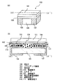
本発明の光センサについて、図1を用いて説明する。
本実施形態では、第1実施形態で示した光センサを配線基板へ搭載する方法について図2を用いて説明する。
本実施形態では、第1実施形態および第2実施形態で示される半導体素子である光セ ンサの受光部について、図3及び図4を用いて説明する。
Claims (7)
- 光センサと、前記光センサに電気的に接続される第1の接続端子とが形成された光透過性及び可とう性を有する第1の基板と、
側面から表面及び裏面に延在するように第2の接続端子が形成された第2の基板と、
第3の接続端子が形成された第3の基板とを有し、
前記光センサと前記第2の基板は第1の接着部材で、向かい合う全面で接着され、かつ前記第1の接着部材によって前記第1の接続端子と前記第2の接続端子が電気的に接続され、
前記第2の基板と前記第3の基板は第2の接着部材で、前記側面及び前記裏面で接着され、かつ前記第2の接着部材によって前記第2の接続端子と前記第3の接続端子が電気的に接続されていることを特徴とする半導体装置。 - 請求項1において、
前記第2の接着部材は、異方性導電接着剤または異方性導電膜であることを特徴とする半導体装置。 - 光センサと、前記光センサに電気的に接続される第1の接続端子とが形成された光透過性及び可とう性を有する第1の基板と、
側面から表面及び裏面に延在するように第2の接続端子が形成された第2の基板と、
第3の接続端子が形成された第3の基板とを有し、
前記光センサと前記第2の基板は第1の接着部材で、向かい合う全面で接着され、かつ前記第1の接着部材によって前記第1の接続端子と前記第2の接続端子が電気的に接続され、
前記第2の基板と前記第3の基板は第2の接着部材で、前記側面及び前記裏面で接着され、かつ前記第2の接着部材によって前記第2の接続端子と前記第3の接続端子が電気的に接続され、
前記第2の接着部材は導電性ペーストであることを特徴とする半導体装置。 - 請求項1乃至請求項3のいずれか一において、
前記第1の接着部材は、異方性導電接着剤または異方性導電膜であることを特徴とする半導体装置。 - 請求項1乃至請求項4のいずれか一において、
前記第1の基板は、フィルム状の基板、又はシート状の基板であることを特徴とする半導体装置。 - 請求項1乃至請求項5のいずれか一において、
前記光センサは、コンタクト部を有する受光部と、前記受光部と接する第1の電極端子及び第1の電極と、前記第1の電極に電気的に接続する第2の電極端子と、からなり、
前記受光部と前記第1の電極端子は、前記コンタクト部において接していることを特徴とする半導体装置。 - 請求項6において、
前記コンタクト部を複数有することを特徴とする半導体装置。
Priority Applications (1)
| Application Number | Priority Date | Filing Date | Title |
|---|---|---|---|
| JP2004292650A JP4679106B2 (ja) | 2003-10-06 | 2004-10-05 | 半導体装置 |
Applications Claiming Priority (2)
| Application Number | Priority Date | Filing Date | Title |
|---|---|---|---|
| JP2003347678 | 2003-10-06 | ||
| JP2004292650A JP4679106B2 (ja) | 2003-10-06 | 2004-10-05 | 半導体装置 |
Publications (3)
| Publication Number | Publication Date |
|---|---|
| JP2005175436A JP2005175436A (ja) | 2005-06-30 |
| JP2005175436A5 JP2005175436A5 (ja) | 2007-10-11 |
| JP4679106B2 true JP4679106B2 (ja) | 2011-04-27 |
Family
ID=34509704
Family Applications (1)
| Application Number | Title | Priority Date | Filing Date |
|---|---|---|---|
| JP2004292650A Expired - Fee Related JP4679106B2 (ja) | 2003-10-06 | 2004-10-05 | 半導体装置 |
Country Status (5)
| Country | Link |
|---|---|
| US (2) | US7180197B2 (ja) |
| EP (1) | EP1542272B1 (ja) |
| JP (1) | JP4679106B2 (ja) |
| KR (2) | KR20050033434A (ja) |
| CN (1) | CN100499175C (ja) |
Families Citing this family (36)
| Publication number | Priority date | Publication date | Assignee | Title |
|---|---|---|---|---|
| JP2005340647A (ja) * | 2004-05-28 | 2005-12-08 | Nec Compound Semiconductor Devices Ltd | インターポーザ基板、半導体パッケージ及び半導体装置並びにそれらの製造方法 |
| JP2006202938A (ja) * | 2005-01-20 | 2006-08-03 | Kojiro Kobayashi | 半導体装置及びその製造方法 |
| JP4399005B2 (ja) * | 2005-02-03 | 2010-01-13 | パナソニック株式会社 | フリップチップ実装方法及びバンプ形成方法 |
| US7994021B2 (en) | 2006-07-28 | 2011-08-09 | Semiconductor Energy Laboratory Co., Ltd. | Method of manufacturing semiconductor device |
| US7943287B2 (en) * | 2006-07-28 | 2011-05-17 | Semiconductor Energy Laboratory Co., Ltd. | Method for manufacturing display device |
| WO2008023630A1 (en) | 2006-08-24 | 2008-02-28 | Semiconductor Energy Laboratory Co., Ltd. | Method for manufacturing display device |
| US7795154B2 (en) | 2006-08-25 | 2010-09-14 | Semiconductor Energy Laboratory Co., Ltd. | Method for manufacturing semiconductor device that uses laser ablation, to selectively remove one or more material layers |
| US8563431B2 (en) * | 2006-08-25 | 2013-10-22 | Semiconductor Energy Laboratory Co., Ltd. | Method for manufacturing semiconductor device |
| US7651896B2 (en) | 2006-08-30 | 2010-01-26 | Semiconductor Energy Laboratory Co., Ltd. | Method for manufacturing semiconductor device |
| JP5110830B2 (ja) * | 2006-08-31 | 2012-12-26 | 株式会社半導体エネルギー研究所 | 半導体装置の作製方法 |
| US7960261B2 (en) * | 2007-03-23 | 2011-06-14 | Semiconductor Energy Laboratory Co., Ltd. | Method for manufacturing crystalline semiconductor film and method for manufacturing thin film transistor |
| KR101423055B1 (ko) * | 2007-04-18 | 2014-07-25 | 가부시키가이샤 한도오따이 에네루기 켄큐쇼 | 반도체 장치를 갖는 광전 변환 소자 및 이것을 사용한반도체 장치 |
| KR101441346B1 (ko) * | 2007-04-27 | 2014-09-18 | 가부시키가이샤 한도오따이 에네루기 켄큐쇼 | 반도체 장치 및 그 제작 방법 |
| JP4989549B2 (ja) * | 2007-08-24 | 2012-08-01 | 三洋電機株式会社 | 太陽電池及び太陽電池モジュール |
| KR100898503B1 (ko) | 2007-09-04 | 2009-05-20 | 주식회사 아이에스시테크놀러지 | 고주파 인터포저 |
| JP5252472B2 (ja) | 2007-09-28 | 2013-07-31 | シャープ株式会社 | 太陽電池、太陽電池の製造方法、太陽電池モジュールの製造方法および太陽電池モジュール |
| US20100263718A1 (en) | 2007-11-09 | 2010-10-21 | Yoshiya Abiko | Solar cell module and method for manufacturing solar cell module |
| DE102007055017B4 (de) * | 2007-11-14 | 2010-11-04 | Fraunhofer-Gesellschaft zur Förderung der angewandten Forschung e.V. | Verfahren zum Verbinden zweier Fügeflächen und Bauteil mit zwei verbundenen Fügeflächen |
| KR20100093590A (ko) * | 2007-12-17 | 2010-08-25 | 퀄컴 엠이엠스 테크놀로지스, 인크. | 후방 측 간섭계 마스크를 구비한 광전변환장치 |
| US20090278213A1 (en) * | 2008-05-08 | 2009-11-12 | International Business Machines Corporation | Electrode arrays and methods of fabricating the same using printing plates to arrange particles in an array |
| US8207487B2 (en) * | 2008-06-25 | 2012-06-26 | Semiconductor Energy Laboratory Co., Ltd. | Photoelectric conversion device including charge/discharge circuit |
| EP2448008A1 (en) * | 2009-06-22 | 2012-05-02 | Sharp Kabushiki Kaisha | Solar cell, solar cell with wiring sheet attached, and solar cell module |
| CN102804393B (zh) | 2009-06-29 | 2015-04-01 | 夏普株式会社 | 布线板、带有布线板的太阳能电池单元、太阳能电池模块以及布线板卷筒 |
| EP2790230A3 (en) * | 2009-08-27 | 2015-01-14 | National Institute of Advanced Industrial Science and Technology | Integrated multi-junction photovoltaic device, and processes for producing same |
| JP5660122B2 (ja) * | 2010-03-02 | 2015-01-28 | コニカミノルタ株式会社 | 放射線検出パネル、放射線画像検出器、放射線検出パネルの製造方法および放射線画像検出器の製造方法 |
| DE102010027953A1 (de) * | 2010-04-20 | 2011-12-01 | Robert Bosch Gmbh | Verfahren zur Herstellung eines Photovoltaikmoduls mit rückseitenkontaktierten Halbleiterzellen und Photovoltaik-Modul |
| JP2012080085A (ja) | 2010-09-10 | 2012-04-19 | Nichia Chem Ind Ltd | 支持体及びそれを用いた発光装置 |
| CN102810574A (zh) * | 2011-05-31 | 2012-12-05 | 联景光电股份有限公司 | 太阳能电池的电极 |
| CN102569247A (zh) * | 2012-01-17 | 2012-07-11 | 华为终端有限公司 | 集成模块、集成系统板和电子设备 |
| KR102091687B1 (ko) | 2012-07-05 | 2020-03-20 | 가부시키가이샤 한도오따이 에네루기 켄큐쇼 | 발광 장치 및 발광 장치의 제작 방법 |
| KR102173801B1 (ko) | 2012-07-12 | 2020-11-04 | 가부시키가이샤 한도오따이 에네루기 켄큐쇼 | 표시 장치, 및 표시 장치의 제작 방법 |
| US11074025B2 (en) | 2012-09-03 | 2021-07-27 | Semiconductor Energy Laboratory Co., Ltd. | Display device and method for manufacturing the same |
| US11581446B2 (en) * | 2015-10-08 | 2023-02-14 | The Boeing Company | Semiconductor device including an electrically conductive adhesive layer and a bypass diode in a carrier |
| US10879211B2 (en) | 2016-06-30 | 2020-12-29 | R.S.M. Electron Power, Inc. | Method of joining a surface-mount component to a substrate with solder that has been temporarily secured |
| JP2018098487A (ja) * | 2016-12-14 | 2018-06-21 | 株式会社村田製作所 | 半導体モジュール |
| KR102423292B1 (ko) * | 2021-09-07 | 2022-07-20 | 한국기계연구원 | 식각 장치 및 이를 포함하는 인터포저 제조 시스템 |
Citations (12)
| Publication number | Priority date | Publication date | Assignee | Title |
|---|---|---|---|---|
| JPS63122133A (ja) * | 1986-11-11 | 1988-05-26 | Matsushita Electric Ind Co Ltd | 半導体チツプの電気的接続方法 |
| JPH0287558A (ja) * | 1988-09-24 | 1990-03-28 | Murata Mfg Co Ltd | Icチップ |
| JPH0766313A (ja) * | 1993-08-27 | 1995-03-10 | Murata Mfg Co Ltd | 複合電子部品 |
| JPH08201540A (ja) * | 1995-01-31 | 1996-08-09 | Citizen Watch Co Ltd | 太陽電池付き時計の構造 |
| JPH1022329A (ja) * | 1996-07-01 | 1998-01-23 | Mitsui High Tec Inc | 半導体装置 |
| JPH10303464A (ja) * | 1997-04-23 | 1998-11-13 | Citizen Electron Co Ltd | Smd型led |
| JP2000216199A (ja) * | 1999-01-21 | 2000-08-04 | Ricoh Co Ltd | 異方性導電ペ―ストを用いた電子部品の接続方法およびそのためのコレット |
| JP2000323472A (ja) * | 1999-05-06 | 2000-11-24 | Canon Inc | 半導体装置、光電変換装置、及びこれらの製造方法 |
| JP2001358437A (ja) * | 2000-06-15 | 2001-12-26 | Seiko Epson Corp | 半導体装置の実装方法 |
| JP2002313979A (ja) * | 2001-04-09 | 2002-10-25 | Sony Corp | インタポーザおよび電子回路装置 |
| JP2003116066A (ja) * | 2001-10-04 | 2003-04-18 | Sony Corp | 固体撮像装置および固体撮像装置の製造方法 |
| JP2004266271A (ja) * | 2003-02-12 | 2004-09-24 | Matsushita Electric Ind Co Ltd | 電子部品の実装体及びその製造方法 |
Family Cites Families (29)
| Publication number | Priority date | Publication date | Assignee | Title |
|---|---|---|---|---|
| US4423435A (en) * | 1980-10-27 | 1983-12-27 | Texas Instruments Incorporated | Assembly of an electronic device on an insulative substrate |
| DE68926448T2 (de) * | 1988-10-14 | 1996-12-12 | Matsushita Electric Ind Co Ltd | Bildsensor und verfahren zu dessen herstellung |
| US5272376A (en) * | 1990-06-01 | 1993-12-21 | Clarion Co., Ltd. | Electrode structure for a semiconductor device |
| JPH04107955A (ja) * | 1990-08-28 | 1992-04-09 | Matsushita Electric Ind Co Ltd | 電子回路素子の封止方法 |
| US5501989A (en) | 1993-03-22 | 1996-03-26 | Semiconductor Energy Laboratory Co., Ltd. | Method of making semiconductor device/circuit having at least partially crystallized semiconductor layer |
| JP3329512B2 (ja) | 1993-03-22 | 2002-09-30 | 株式会社半導体エネルギー研究所 | 半導体回路およびその作製方法 |
| JP3150840B2 (ja) * | 1994-03-11 | 2001-03-26 | 株式会社半導体エネルギー研究所 | 半導体装置の作製方法 |
| US6700133B1 (en) * | 1994-03-11 | 2004-03-02 | Semiconductor Energy Laboratory Co., Ltd. | Method for producing semiconductor device |
| US5672545A (en) * | 1994-08-08 | 1997-09-30 | Santa Barbara Research Center | Thermally matched flip-chip detector assembly and method |
| JP2900229B2 (ja) * | 1994-12-27 | 1999-06-02 | 株式会社半導体エネルギー研究所 | 半導体装置およびその作製方法および電気光学装置 |
| JP3825475B2 (ja) * | 1995-06-30 | 2006-09-27 | 株式会社 東芝 | 電子部品の製造方法 |
| JPH0945805A (ja) * | 1995-07-31 | 1997-02-14 | Fujitsu Ltd | 配線基板、半導体装置及び半導体装置を配線基板から取り外す方法並びに半導体装置の製造方法 |
| JP3183390B2 (ja) * | 1995-09-05 | 2001-07-09 | キヤノン株式会社 | 光電変換装置及びそれを用いた撮像装置 |
| US6461890B1 (en) * | 1996-12-27 | 2002-10-08 | Rohm Co., Ltd. | Structure of semiconductor chip suitable for chip-on-board system and methods of fabricating and mounting the same |
| US5783465A (en) * | 1997-04-03 | 1998-07-21 | Lucent Technologies Inc. | Compliant bump technology |
| US5965064A (en) * | 1997-10-28 | 1999-10-12 | Sony Chemicals Corporation | Anisotropically electroconductive adhesive and adhesive film |
| SG71734A1 (en) * | 1997-11-21 | 2000-04-18 | Inst Materials Research & Eng | Area array stud bump flip chip and assembly process |
| JP4085459B2 (ja) * | 1998-03-02 | 2008-05-14 | セイコーエプソン株式会社 | 3次元デバイスの製造方法 |
| US6879014B2 (en) * | 2000-03-20 | 2005-04-12 | Aegis Semiconductor, Inc. | Semitransparent optical detector including a polycrystalline layer and method of making |
| JP3597754B2 (ja) * | 2000-04-24 | 2004-12-08 | Necエレクトロニクス株式会社 | 半導体装置及びその製造方法 |
| JP2002094082A (ja) * | 2000-07-11 | 2002-03-29 | Seiko Epson Corp | 光素子及びその製造方法並びに電子機器 |
| US6624921B1 (en) * | 2001-03-12 | 2003-09-23 | Amkor Technology, Inc. | Micromirror device package fabrication method |
| JP2003045236A (ja) | 2001-08-03 | 2003-02-14 | Nec Kagoshima Ltd | 異方性導電フイルムおよびこれを用いた集積回路デバイスの接続方法 |
| JP2003060744A (ja) | 2001-08-21 | 2003-02-28 | Sanyo Electric Co Ltd | 携帯機器 |
| US6555917B1 (en) * | 2001-10-09 | 2003-04-29 | Amkor Technology, Inc. | Semiconductor package having stacked semiconductor chips and method of making the same |
| JP5030360B2 (ja) * | 2002-12-25 | 2012-09-19 | オリンパス株式会社 | 固体撮像装置の製造方法 |
| JP3972825B2 (ja) | 2003-01-28 | 2007-09-05 | セイコーエプソン株式会社 | アクティブマトリクス型表示装置の製造方法 |
| US20040156177A1 (en) * | 2003-02-12 | 2004-08-12 | Matsushita Electric Industrial Co., Ltd. | Package of electronic components and method for producing the same |
| JP3693060B2 (ja) * | 2003-09-24 | 2005-09-07 | セイコーエプソン株式会社 | 半導体装置及びその製造方法、回路基板並びに電子機器 |
-
2004
- 2004-09-15 EP EP04021934.7A patent/EP1542272B1/en not_active Not-in-force
- 2004-09-29 US US10/951,811 patent/US7180197B2/en active Active
- 2004-09-30 KR KR1020040077760A patent/KR20050033434A/ko active Search and Examination
- 2004-10-05 JP JP2004292650A patent/JP4679106B2/ja not_active Expired - Fee Related
- 2004-10-08 CN CNB2004100874789A patent/CN100499175C/zh not_active Expired - Fee Related
-
2006
- 2006-08-03 US US11/498,164 patent/US8481370B2/en active Active
-
2009
- 2009-09-02 KR KR1020090082612A patent/KR20090114343A/ko active Search and Examination
Patent Citations (12)
| Publication number | Priority date | Publication date | Assignee | Title |
|---|---|---|---|---|
| JPS63122133A (ja) * | 1986-11-11 | 1988-05-26 | Matsushita Electric Ind Co Ltd | 半導体チツプの電気的接続方法 |
| JPH0287558A (ja) * | 1988-09-24 | 1990-03-28 | Murata Mfg Co Ltd | Icチップ |
| JPH0766313A (ja) * | 1993-08-27 | 1995-03-10 | Murata Mfg Co Ltd | 複合電子部品 |
| JPH08201540A (ja) * | 1995-01-31 | 1996-08-09 | Citizen Watch Co Ltd | 太陽電池付き時計の構造 |
| JPH1022329A (ja) * | 1996-07-01 | 1998-01-23 | Mitsui High Tec Inc | 半導体装置 |
| JPH10303464A (ja) * | 1997-04-23 | 1998-11-13 | Citizen Electron Co Ltd | Smd型led |
| JP2000216199A (ja) * | 1999-01-21 | 2000-08-04 | Ricoh Co Ltd | 異方性導電ペ―ストを用いた電子部品の接続方法およびそのためのコレット |
| JP2000323472A (ja) * | 1999-05-06 | 2000-11-24 | Canon Inc | 半導体装置、光電変換装置、及びこれらの製造方法 |
| JP2001358437A (ja) * | 2000-06-15 | 2001-12-26 | Seiko Epson Corp | 半導体装置の実装方法 |
| JP2002313979A (ja) * | 2001-04-09 | 2002-10-25 | Sony Corp | インタポーザおよび電子回路装置 |
| JP2003116066A (ja) * | 2001-10-04 | 2003-04-18 | Sony Corp | 固体撮像装置および固体撮像装置の製造方法 |
| JP2004266271A (ja) * | 2003-02-12 | 2004-09-24 | Matsushita Electric Ind Co Ltd | 電子部品の実装体及びその製造方法 |
Also Published As
| Publication number | Publication date |
|---|---|
| EP1542272A2 (en) | 2005-06-15 |
| CN100499175C (zh) | 2009-06-10 |
| EP1542272B1 (en) | 2016-07-20 |
| KR20050033434A (ko) | 2005-04-12 |
| US20050082655A1 (en) | 2005-04-21 |
| EP1542272A3 (en) | 2012-03-07 |
| JP2005175436A (ja) | 2005-06-30 |
| US8481370B2 (en) | 2013-07-09 |
| US7180197B2 (en) | 2007-02-20 |
| US20060270114A1 (en) | 2006-11-30 |
| KR20090114343A (ko) | 2009-11-03 |
| CN1606169A (zh) | 2005-04-13 |
Similar Documents
| Publication | Publication Date | Title |
|---|---|---|
| JP4679106B2 (ja) | 半導体装置 | |
| US7851278B2 (en) | Semiconductor device and method for manufacturing the same | |
| US20210227061A1 (en) | Light-emitting device | |
| JP4481135B2 (ja) | 半導体装置及びその作製方法 | |
| US7923800B2 (en) | Semiconductor device and electronic device | |
| CN101233624B (zh) | 交流发光器件 | |
| CN104115266A (zh) | 转移并键合微型器件阵列的方法 | |
| TW201605038A (zh) | 顯示模組、顯示裝置及製造顯示模組的方法 | |
| US10141537B2 (en) | Display panel and manufacturing method therefor, and display apparatus | |
| TW200824152A (en) | Electronic component, manufacturing method of the electronic component, electronic component assembly body, and electronic device | |
| TW201212303A (en) | LED packaging structure and packaging method thereof | |
| TW200406894A (en) | Semiconductor device and optoelectronic device | |
| KR101441346B1 (ko) | 반도체 장치 및 그 제작 방법 | |
| KR20210108526A (ko) | 표시 장치 | |
| TW202350022A (zh) | 電子裝置 | |
| CN117012799A (zh) | 驱动背板及显示面板 | |
| JP2007304299A (ja) | 薄膜回路装置およびその製造方法、並びに電子機器 | |
| KR20220142938A (ko) | 반도체장치, 표시장치, 촬상장치, 및 전자기기 | |
| CN113990884A (zh) | 驱动基板及其制备方法和显示装置 |
Legal Events
| Date | Code | Title | Description |
|---|---|---|---|
| A521 | Request for written amendment filed |
Free format text: JAPANESE INTERMEDIATE CODE: A523 Effective date: 20070829 |
|
| A621 | Written request for application examination |
Free format text: JAPANESE INTERMEDIATE CODE: A621 Effective date: 20070829 |
|
| A977 | Report on retrieval |
Free format text: JAPANESE INTERMEDIATE CODE: A971007 Effective date: 20080201 |
|
| A131 | Notification of reasons for refusal |
Free format text: JAPANESE INTERMEDIATE CODE: A131 Effective date: 20100817 |
|
| A521 | Request for written amendment filed |
Free format text: JAPANESE INTERMEDIATE CODE: A523 Effective date: 20101007 |
|
| A131 | Notification of reasons for refusal |
Free format text: JAPANESE INTERMEDIATE CODE: A131 Effective date: 20101102 |
|
| A521 | Request for written amendment filed |
Free format text: JAPANESE INTERMEDIATE CODE: A523 Effective date: 20101223 |
|
| TRDD | Decision of grant or rejection written | ||
| A01 | Written decision to grant a patent or to grant a registration (utility model) |
Free format text: JAPANESE INTERMEDIATE CODE: A01 Effective date: 20110125 |
|
| A01 | Written decision to grant a patent or to grant a registration (utility model) |
Free format text: JAPANESE INTERMEDIATE CODE: A01 |
|
| A61 | First payment of annual fees (during grant procedure) |
Free format text: JAPANESE INTERMEDIATE CODE: A61 Effective date: 20110201 |
|
| R150 | Certificate of patent or registration of utility model |
Free format text: JAPANESE INTERMEDIATE CODE: R150 |
|
| FPAY | Renewal fee payment (event date is renewal date of database) |
Free format text: PAYMENT UNTIL: 20140210 Year of fee payment: 3 |
|
| FPAY | Renewal fee payment (event date is renewal date of database) |
Free format text: PAYMENT UNTIL: 20140210 Year of fee payment: 3 |
|
| R250 | Receipt of annual fees |
Free format text: JAPANESE INTERMEDIATE CODE: R250 |
|
| R250 | Receipt of annual fees |
Free format text: JAPANESE INTERMEDIATE CODE: R250 |
|
| R250 | Receipt of annual fees |
Free format text: JAPANESE INTERMEDIATE CODE: R250 |
|
| R250 | Receipt of annual fees |
Free format text: JAPANESE INTERMEDIATE CODE: R250 |
|
| LAPS | Cancellation because of no payment of annual fees |