JP4481135B2 - 半導体装置及びその作製方法 - Google Patents
半導体装置及びその作製方法 Download PDFInfo
- Publication number
- JP4481135B2 JP4481135B2 JP2004292643A JP2004292643A JP4481135B2 JP 4481135 B2 JP4481135 B2 JP 4481135B2 JP 2004292643 A JP2004292643 A JP 2004292643A JP 2004292643 A JP2004292643 A JP 2004292643A JP 4481135 B2 JP4481135 B2 JP 4481135B2
- Authority
- JP
- Japan
- Prior art keywords
- semiconductor
- semiconductor device
- substrate
- electrode
- insulating film
- Prior art date
- Legal status (The legal status is an assumption and is not a legal conclusion. Google has not performed a legal analysis and makes no representation as to the accuracy of the status listed.)
- Expired - Fee Related
Links
Images


Classifications
-
- H—ELECTRICITY
- H01—ELECTRIC ELEMENTS
- H01L—SEMICONDUCTOR DEVICES NOT COVERED BY CLASS H10
- H01L2224/00—Indexing scheme for arrangements for connecting or disconnecting semiconductor or solid-state bodies and methods related thereto as covered by H01L24/00
- H01L2224/01—Means for bonding being attached to, or being formed on, the surface to be connected, e.g. chip-to-package, die-attach, "first-level" interconnects; Manufacturing methods related thereto
- H01L2224/10—Bump connectors; Manufacturing methods related thereto
- H01L2224/15—Structure, shape, material or disposition of the bump connectors after the connecting process
- H01L2224/16—Structure, shape, material or disposition of the bump connectors after the connecting process of an individual bump connector
- H01L2224/161—Disposition
- H01L2224/16151—Disposition the bump connector connecting between a semiconductor or solid-state body and an item not being a semiconductor or solid-state body, e.g. chip-to-substrate, chip-to-passive
- H01L2224/16221—Disposition the bump connector connecting between a semiconductor or solid-state body and an item not being a semiconductor or solid-state body, e.g. chip-to-substrate, chip-to-passive the body and the item being stacked
- H01L2224/16225—Disposition the bump connector connecting between a semiconductor or solid-state body and an item not being a semiconductor or solid-state body, e.g. chip-to-substrate, chip-to-passive the body and the item being stacked the item being non-metallic, e.g. insulating substrate with or without metallisation
Description
本実施形態では、プラスチック基板に形成され、側面に凹部を有する光セン サについて、図1を用いて説明する。
ここでは、受光部で検出した電流を増幅する回路を有する光センサについて図2を用いて説明する。なお、ここでは、増幅回路を構成する素子として薄膜トランジスタ(以下、TFT(Thin Film Transistor)と示す。)を用いたものを示すが、これに限定されるものではなく、演算増幅器(オペアンプ)等を用いることができる。
次に、第2実施形態における光センサの駆動回路の一例を図3を用いて示す。本実施形態では、光センサは増幅回路としてカレントミレラー回路を用いている。
本実施形態では、第1実施形態乃至第3実施形態で示される光センサの作製工程を、図4を用いて示す。
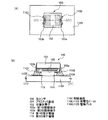
本実施形態では、第1実施形態乃至第4実施形態で形成された光センサを配線基板へ搭載する方法について図5を用いて説明する。
Claims (12)
- プラスチック、ガラス、又は有機樹脂でなる基板上に形成される半導体素子、前記半導体素子を覆う絶縁膜、及び前記半導体素子と電気的に接続される導電膜を有し、
前記基板および前記絶縁膜の側面は凹部を有し、
前記導電膜は、前記凹部に形成されていることを特徴とする半導体装置。 - プラスチック、ガラス、又は有機樹脂でなる基板上に形成される半導体素子、前記半導体素子と電気的に接続する電極端子、前記半導体素子及び前記電極端子を覆う絶縁膜、及び前記電極端子と電気的に接続する接続端子を有し、
前記基板および前記絶縁膜の側面は凹部を有し、
前記接続端子は、前記凹部に形成されていることを特徴とする半導体装置。 - プラスチック、ガラス、又は有機樹脂でなる基板上に形成される半導体素子、前記半導体素子を覆う絶縁膜、及び前記半導体素子と電気的に接続される導電膜を有し、
前記基板および前記絶縁膜の側面は凹部を有し、
前記導電膜は、前記側面に隣接する面に接し、かつ、前記凹部に形成されていることを特徴とする半導体装置。 - プラスチック、ガラス、又は有機樹脂でなる基板上に形成される半導体素子、前記半導体素子と電気的に接続される電極端子、前記半導体素子及び前記電極端子を覆う絶縁膜、及び前記絶縁膜を介して前記電極端子と電気的に接続する接続端子を有し、
前記基板および前記絶縁膜の側面は凹部を有し、
前記接続端子は、前記側面に隣接する面に接し、かつ、前記凹部に形成されていることを特徴とする半導体装置。 - 請求項1乃至請求項4のいずれか一項において、前記凹部を有する前記側面は傾斜を有することを特徴とする半導体装置。
- 請求項1乃至請求項5のいずれか一項において、前記凹部は曲面又は平面を有することを特徴とする半導体装置。
- 請求項1乃至請求項6のいずれか一項において、前記半導体素子は、半導体薄膜を有し、前記半導体薄膜は微結晶でなることを特徴とする半導体装置。
- 請求項1乃至請求項7のいずれか一項において、前記導電膜又は前記接続端子は、ニッケル、銅、亜鉛、パラジウム、銀、スズ、白金、又は金から選ばれた一元素、又は該元素を含む合金で形成されていることを特徴とする半導体装置。
- 請求項1乃至請求項8のいずれか一項において、前記半導体素子は、薄膜トランジスタ、又はダイオードを有することを特徴とする半導体装置。
- 請求項1乃至請求項9のいずれか一項において、前記半導体装置は、光センサ、光電変換装置、太陽電池、又は薄膜トランジスタを用いて形成された集積回路であることを特徴とする半導体装置。
- プラスチック、ガラス、又は有機樹脂でなる基板上に半導体素子を形成し、
前記半導体素子を覆う絶縁膜を形成し、
前記基板、及び前記絶縁膜に、前記半導体素子の両脇に側面が凹部となる開口部を形成し、
前記開口部に前記半導体素子と電気的に接続される導電膜を形成し、
前記基板を前記開口部が形成されている領域と前記半導体素子が形成されていない領域で切断することを特徴とする半導体装置の作製方法。 - 請求項11において、前記基板にレーザ光を照射して前記開口部を形成することを特徴とする半導体装置の作製方法。
Priority Applications (1)
| Application Number | Priority Date | Filing Date | Title |
|---|---|---|---|
| JP2004292643A JP4481135B2 (ja) | 2003-10-06 | 2004-10-05 | 半導体装置及びその作製方法 |
Applications Claiming Priority (2)
| Application Number | Priority Date | Filing Date | Title |
|---|---|---|---|
| JP2003347676 | 2003-10-06 | ||
| JP2004292643A JP4481135B2 (ja) | 2003-10-06 | 2004-10-05 | 半導体装置及びその作製方法 |
Publications (3)
| Publication Number | Publication Date |
|---|---|
| JP2005136394A JP2005136394A (ja) | 2005-05-26 |
| JP2005136394A5 JP2005136394A5 (ja) | 2007-08-16 |
| JP4481135B2 true JP4481135B2 (ja) | 2010-06-16 |
Family
ID=34655940
Family Applications (1)
| Application Number | Title | Priority Date | Filing Date |
|---|---|---|---|
| JP2004292643A Expired - Fee Related JP4481135B2 (ja) | 2003-10-06 | 2004-10-05 | 半導体装置及びその作製方法 |
Country Status (1)
| Country | Link |
|---|---|
| JP (1) | JP4481135B2 (ja) |
Families Citing this family (15)
| Publication number | Priority date | Publication date | Assignee | Title |
|---|---|---|---|---|
| US7492028B2 (en) | 2005-02-18 | 2009-02-17 | Semiconductor Energy Laboratory Co., Ltd. | Photoelectric conversion device and manufacturing method of the same, and a semiconductor device |
| JP4532418B2 (ja) * | 2005-02-18 | 2010-08-25 | 株式会社半導体エネルギー研究所 | 光センサ及びその作製方法 |
| EP1724844A2 (en) | 2005-05-20 | 2006-11-22 | Semiconductor Energy Laboratory Co., Ltd. | Photoelectric conversion device, manufacturing method thereof and semiconductor device |
| EP1727120B1 (en) | 2005-05-23 | 2008-07-09 | Semiconductor Energy Laboratory Co., Ltd. | Photoelectric conversion device and manufacturing method thereof |
| JP5082036B2 (ja) * | 2005-10-31 | 2012-11-28 | 株式会社リキッド・デザイン・システムズ | 半導体装置の製造方法および半導体装置 |
| WO2007125977A1 (en) * | 2006-04-27 | 2007-11-08 | Semiconductor Energy Laboratory Co., Ltd. | Semiconductor device and electronic appliance using the same |
| US8514165B2 (en) | 2006-12-28 | 2013-08-20 | Semiconductor Energy Laboratory Co., Ltd. | Semiconductor device |
| US8207589B2 (en) * | 2007-02-15 | 2012-06-26 | Semiconductor Energy Laboratory Co., Ltd. | Photoelectric conversion device and electronic device, and method for manufacturing photoelectric conversion device |
| US8354724B2 (en) | 2007-03-26 | 2013-01-15 | Semiconductor Energy Laboratory Co., Ltd. | Semiconductor device and electronic device |
| JP5355915B2 (ja) * | 2007-04-18 | 2013-11-27 | 株式会社半導体エネルギー研究所 | 半導体装置 |
| WO2009014155A1 (en) | 2007-07-25 | 2009-01-29 | Semiconductor Energy Laboratory Co., Ltd. | Photoelectric conversion device and electronic device having the same |
| WO2015049852A1 (ja) | 2013-10-01 | 2015-04-09 | パナソニックIpマネジメント株式会社 | 半導体装置 |
| TWI656631B (zh) * | 2014-03-28 | 2019-04-11 | 日商半導體能源研究所股份有限公司 | 攝像裝置 |
| CN107112315B (zh) * | 2015-01-16 | 2019-03-29 | 雫石诚 | 半导体器件及其制造方法 |
| JP2021072583A (ja) | 2019-10-31 | 2021-05-06 | 株式会社村田製作所 | 高周波モジュール及び通信装置 |
Citations (6)
| Publication number | Priority date | Publication date | Assignee | Title |
|---|---|---|---|---|
| JPH05326618A (ja) * | 1992-05-15 | 1993-12-10 | Rohm Co Ltd | 半導体装置 |
| JPH09129780A (ja) * | 1995-09-01 | 1997-05-16 | Canon Inc | Icパッケージ、光センサicパッケージおよびこれらの組立方法 |
| JPH10189481A (ja) * | 1996-11-07 | 1998-07-21 | Semiconductor Energy Lab Co Ltd | 半導体装置の作製方法 |
| JP2000196117A (ja) * | 1992-09-11 | 2000-07-14 | Semiconductor Energy Lab Co Ltd | 光電変換装置の作製方法 |
| JP2001036097A (ja) * | 2000-01-01 | 2001-02-09 | Semiconductor Energy Lab Co Ltd | 半導体装置 |
| JP2001068513A (ja) * | 1999-08-30 | 2001-03-16 | Sharp Corp | 半導体装置 |
-
2004
- 2004-10-05 JP JP2004292643A patent/JP4481135B2/ja not_active Expired - Fee Related
Patent Citations (6)
| Publication number | Priority date | Publication date | Assignee | Title |
|---|---|---|---|---|
| JPH05326618A (ja) * | 1992-05-15 | 1993-12-10 | Rohm Co Ltd | 半導体装置 |
| JP2000196117A (ja) * | 1992-09-11 | 2000-07-14 | Semiconductor Energy Lab Co Ltd | 光電変換装置の作製方法 |
| JPH09129780A (ja) * | 1995-09-01 | 1997-05-16 | Canon Inc | Icパッケージ、光センサicパッケージおよびこれらの組立方法 |
| JPH10189481A (ja) * | 1996-11-07 | 1998-07-21 | Semiconductor Energy Lab Co Ltd | 半導体装置の作製方法 |
| JP2001068513A (ja) * | 1999-08-30 | 2001-03-16 | Sharp Corp | 半導体装置 |
| JP2001036097A (ja) * | 2000-01-01 | 2001-02-09 | Semiconductor Energy Lab Co Ltd | 半導体装置 |
Also Published As
| Publication number | Publication date |
|---|---|
| JP2005136394A (ja) | 2005-05-26 |
Similar Documents
| Publication | Publication Date | Title |
|---|---|---|
| US7851278B2 (en) | Semiconductor device and method for manufacturing the same | |
| US8481370B2 (en) | Semiconductor device and method for manufacturing the same | |
| JP4481135B2 (ja) | 半導体装置及びその作製方法 | |
| KR101273971B1 (ko) | 반도체장치 및 그 제조방법 | |
| JP5784096B2 (ja) | 半導体装置の作製方法 | |
| KR101467973B1 (ko) | 반도체 장치 및 표시 장치 | |
| TWI392102B (zh) | 半導體裝置 | |
| KR101232663B1 (ko) | 광전 변환 장치, 그 제조 방법 및 반도체 장치 | |
| US7888714B2 (en) | Semiconductor device and method of manufacturing the same | |
| US7923800B2 (en) | Semiconductor device and electronic device | |
| KR20040045354A (ko) | 반도체 디바이스, 디스플레이 디바이스, 및 발광디바이스와 그 제조 방법 | |
| JP4809715B2 (ja) | 光電変換装置及びその作製方法、並びに半導体装置 | |
| JP2005136392A (ja) | 半導体装置およびその作製方法 |
Legal Events
| Date | Code | Title | Description |
|---|---|---|---|
| A521 | Request for written amendment filed |
Free format text: JAPANESE INTERMEDIATE CODE: A523 Effective date: 20070704 |
|
| A621 | Written request for application examination |
Free format text: JAPANESE INTERMEDIATE CODE: A621 Effective date: 20070704 |
|
| A977 | Report on retrieval |
Free format text: JAPANESE INTERMEDIATE CODE: A971007 Effective date: 20090519 |
|
| A131 | Notification of reasons for refusal |
Free format text: JAPANESE INTERMEDIATE CODE: A131 Effective date: 20090526 |
|
| A521 | Request for written amendment filed |
Free format text: JAPANESE INTERMEDIATE CODE: A523 Effective date: 20090723 |
|
| TRDD | Decision of grant or rejection written | ||
| A01 | Written decision to grant a patent or to grant a registration (utility model) |
Free format text: JAPANESE INTERMEDIATE CODE: A01 Effective date: 20100316 |
|
| A01 | Written decision to grant a patent or to grant a registration (utility model) |
Free format text: JAPANESE INTERMEDIATE CODE: A01 |
|
| A61 | First payment of annual fees (during grant procedure) |
Free format text: JAPANESE INTERMEDIATE CODE: A61 Effective date: 20100317 |
|
| FPAY | Renewal fee payment (event date is renewal date of database) |
Free format text: PAYMENT UNTIL: 20130326 Year of fee payment: 3 |
|
| R150 | Certificate of patent or registration of utility model |
Ref document number: 4481135 Country of ref document: JP Free format text: JAPANESE INTERMEDIATE CODE: R150 Free format text: JAPANESE INTERMEDIATE CODE: R150 |
|
| FPAY | Renewal fee payment (event date is renewal date of database) |
Free format text: PAYMENT UNTIL: 20130326 Year of fee payment: 3 |
|
| FPAY | Renewal fee payment (event date is renewal date of database) |
Free format text: PAYMENT UNTIL: 20130326 Year of fee payment: 3 |
|
| FPAY | Renewal fee payment (event date is renewal date of database) |
Free format text: PAYMENT UNTIL: 20140326 Year of fee payment: 4 |
|
| R250 | Receipt of annual fees |
Free format text: JAPANESE INTERMEDIATE CODE: R250 |
|
| R250 | Receipt of annual fees |
Free format text: JAPANESE INTERMEDIATE CODE: R250 |
|
| R250 | Receipt of annual fees |
Free format text: JAPANESE INTERMEDIATE CODE: R250 |
|
| R250 | Receipt of annual fees |
Free format text: JAPANESE INTERMEDIATE CODE: R250 |
|
| R250 | Receipt of annual fees |
Free format text: JAPANESE INTERMEDIATE CODE: R250 |
|
| R250 | Receipt of annual fees |
Free format text: JAPANESE INTERMEDIATE CODE: R250 |
|
| LAPS | Cancellation because of no payment of annual fees |