JP4453702B2 - 複合型電子部品及びその製造方法 - Google Patents
複合型電子部品及びその製造方法 Download PDFInfo
- Publication number
- JP4453702B2 JP4453702B2 JP2006527819A JP2006527819A JP4453702B2 JP 4453702 B2 JP4453702 B2 JP 4453702B2 JP 2006527819 A JP2006527819 A JP 2006527819A JP 2006527819 A JP2006527819 A JP 2006527819A JP 4453702 B2 JP4453702 B2 JP 4453702B2
- Authority
- JP
- Japan
- Prior art keywords
- electronic component
- chip
- block
- type electronic
- multilayer
- Prior art date
- Legal status (The legal status is an assumption and is not a legal conclusion. Google has not performed a legal analysis and makes no representation as to the accuracy of the status listed.)
- Expired - Fee Related
Links
Images


Classifications
-
- H—ELECTRICITY
- H01—ELECTRIC ELEMENTS
- H01L—SEMICONDUCTOR DEVICES NOT COVERED BY CLASS H10
- H01L23/00—Details of semiconductor or other solid state devices
- H01L23/48—Arrangements for conducting electric current to or from the solid state body in operation, e.g. leads, terminal arrangements ; Selection of materials therefor
- H01L23/488—Arrangements for conducting electric current to or from the solid state body in operation, e.g. leads, terminal arrangements ; Selection of materials therefor consisting of soldered or bonded constructions
- H01L23/498—Leads, i.e. metallisations or lead-frames on insulating substrates, e.g. chip carriers
- H01L23/49822—Multilayer substrates
-
- H—ELECTRICITY
- H01—ELECTRIC ELEMENTS
- H01L—SEMICONDUCTOR DEVICES NOT COVERED BY CLASS H10
- H01L23/00—Details of semiconductor or other solid state devices
- H01L23/52—Arrangements for conducting electric current within the device in operation from one component to another, i.e. interconnections, e.g. wires, lead frames
- H01L23/538—Arrangements for conducting electric current within the device in operation from one component to another, i.e. interconnections, e.g. wires, lead frames the interconnection structure between a plurality of semiconductor chips being formed on, or in, insulating substrates
- H01L23/5385—Assembly of a plurality of insulating substrates
-
- H—ELECTRICITY
- H01—ELECTRIC ELEMENTS
- H01L—SEMICONDUCTOR DEVICES NOT COVERED BY CLASS H10
- H01L23/00—Details of semiconductor or other solid state devices
- H01L23/552—Protection against radiation, e.g. light or electromagnetic waves
-
- H—ELECTRICITY
- H01—ELECTRIC ELEMENTS
- H01L—SEMICONDUCTOR DEVICES NOT COVERED BY CLASS H10
- H01L25/00—Assemblies consisting of a plurality of individual semiconductor or other solid state devices ; Multistep manufacturing processes thereof
- H01L25/16—Assemblies consisting of a plurality of individual semiconductor or other solid state devices ; Multistep manufacturing processes thereof the devices being of types provided for in two or more different main groups of groups H01L27/00 - H01L33/00, or in a single subclass of H10K, H10N, e.g. forming hybrid circuits
-
- H—ELECTRICITY
- H05—ELECTRIC TECHNIQUES NOT OTHERWISE PROVIDED FOR
- H05K—PRINTED CIRCUITS; CASINGS OR CONSTRUCTIONAL DETAILS OF ELECTRIC APPARATUS; MANUFACTURE OF ASSEMBLAGES OF ELECTRICAL COMPONENTS
- H05K1/00—Printed circuits
- H05K1/02—Details
- H05K1/14—Structural association of two or more printed circuits
- H05K1/141—One or more single auxiliary printed circuits mounted on a main printed circuit, e.g. modules, adapters
-
- H—ELECTRICITY
- H05—ELECTRIC TECHNIQUES NOT OTHERWISE PROVIDED FOR
- H05K—PRINTED CIRCUITS; CASINGS OR CONSTRUCTIONAL DETAILS OF ELECTRIC APPARATUS; MANUFACTURE OF ASSEMBLAGES OF ELECTRICAL COMPONENTS
- H05K1/00—Printed circuits
- H05K1/02—Details
- H05K1/14—Structural association of two or more printed circuits
- H05K1/142—Arrangements of planar printed circuit boards in the same plane, e.g. auxiliary printed circuit insert mounted in a main printed circuit
-
- H—ELECTRICITY
- H05—ELECTRIC TECHNIQUES NOT OTHERWISE PROVIDED FOR
- H05K—PRINTED CIRCUITS; CASINGS OR CONSTRUCTIONAL DETAILS OF ELECTRIC APPARATUS; MANUFACTURE OF ASSEMBLAGES OF ELECTRICAL COMPONENTS
- H05K1/00—Printed circuits
- H05K1/18—Printed circuits structurally associated with non-printed electric components
- H05K1/182—Printed circuits structurally associated with non-printed electric components associated with components mounted in the printed circuit board, e.g. insert mounted components [IMC]
- H05K1/185—Components encapsulated in the insulating substrate of the printed circuit or incorporated in internal layers of a multilayer circuit
- H05K1/186—Components encapsulated in the insulating substrate of the printed circuit or incorporated in internal layers of a multilayer circuit manufactured by mounting on or connecting to patterned circuits before or during embedding
- H05K1/187—Components encapsulated in the insulating substrate of the printed circuit or incorporated in internal layers of a multilayer circuit manufactured by mounting on or connecting to patterned circuits before or during embedding the patterned circuits being prefabricated circuits, which are not yet attached to a permanent insulating substrate, e.g. on a temporary carrier
-
- H—ELECTRICITY
- H05—ELECTRIC TECHNIQUES NOT OTHERWISE PROVIDED FOR
- H05K—PRINTED CIRCUITS; CASINGS OR CONSTRUCTIONAL DETAILS OF ELECTRIC APPARATUS; MANUFACTURE OF ASSEMBLAGES OF ELECTRICAL COMPONENTS
- H05K3/00—Apparatus or processes for manufacturing printed circuits
- H05K3/46—Manufacturing multilayer circuits
- H05K3/4688—Composite multilayer circuits, i.e. comprising insulating layers having different properties
- H05K3/4694—Partitioned multilayer circuits having adjacent regions with different properties, e.g. by adding or inserting locally circuit layers having a higher circuit density
-
- H—ELECTRICITY
- H01—ELECTRIC ELEMENTS
- H01L—SEMICONDUCTOR DEVICES NOT COVERED BY CLASS H10
- H01L2224/00—Indexing scheme for arrangements for connecting or disconnecting semiconductor or solid-state bodies and methods related thereto as covered by H01L24/00
- H01L2224/01—Means for bonding being attached to, or being formed on, the surface to be connected, e.g. chip-to-package, die-attach, "first-level" interconnects; Manufacturing methods related thereto
- H01L2224/10—Bump connectors; Manufacturing methods related thereto
- H01L2224/15—Structure, shape, material or disposition of the bump connectors after the connecting process
- H01L2224/16—Structure, shape, material or disposition of the bump connectors after the connecting process of an individual bump connector
- H01L2224/161—Disposition
- H01L2224/16151—Disposition the bump connector connecting between a semiconductor or solid-state body and an item not being a semiconductor or solid-state body, e.g. chip-to-substrate, chip-to-passive
- H01L2224/16221—Disposition the bump connector connecting between a semiconductor or solid-state body and an item not being a semiconductor or solid-state body, e.g. chip-to-substrate, chip-to-passive the body and the item being stacked
- H01L2224/16225—Disposition the bump connector connecting between a semiconductor or solid-state body and an item not being a semiconductor or solid-state body, e.g. chip-to-substrate, chip-to-passive the body and the item being stacked the item being non-metallic, e.g. insulating substrate with or without metallisation
-
- H—ELECTRICITY
- H01—ELECTRIC ELEMENTS
- H01L—SEMICONDUCTOR DEVICES NOT COVERED BY CLASS H10
- H01L2924/00—Indexing scheme for arrangements or methods for connecting or disconnecting semiconductor or solid-state bodies as covered by H01L24/00
- H01L2924/095—Indexing scheme for arrangements or methods for connecting or disconnecting semiconductor or solid-state bodies as covered by H01L24/00 with a principal constituent of the material being a combination of two or more materials provided in the groups H01L2924/013 - H01L2924/0715
- H01L2924/097—Glass-ceramics, e.g. devitrified glass
- H01L2924/09701—Low temperature co-fired ceramic [LTCC]
-
- H—ELECTRICITY
- H01—ELECTRIC ELEMENTS
- H01L—SEMICONDUCTOR DEVICES NOT COVERED BY CLASS H10
- H01L2924/00—Indexing scheme for arrangements or methods for connecting or disconnecting semiconductor or solid-state bodies as covered by H01L24/00
- H01L2924/15—Details of package parts other than the semiconductor or other solid state devices to be connected
- H01L2924/151—Die mounting substrate
- H01L2924/1517—Multilayer substrate
- H01L2924/15192—Resurf arrangement of the internal vias
-
- H—ELECTRICITY
- H01—ELECTRIC ELEMENTS
- H01L—SEMICONDUCTOR DEVICES NOT COVERED BY CLASS H10
- H01L2924/00—Indexing scheme for arrangements or methods for connecting or disconnecting semiconductor or solid-state bodies as covered by H01L24/00
- H01L2924/19—Details of hybrid assemblies other than the semiconductor or other solid state devices to be connected
- H01L2924/191—Disposition
- H01L2924/19101—Disposition of discrete passive components
- H01L2924/19105—Disposition of discrete passive components in a side-by-side arrangement on a common die mounting substrate
-
- H—ELECTRICITY
- H05—ELECTRIC TECHNIQUES NOT OTHERWISE PROVIDED FOR
- H05K—PRINTED CIRCUITS; CASINGS OR CONSTRUCTIONAL DETAILS OF ELECTRIC APPARATUS; MANUFACTURE OF ASSEMBLAGES OF ELECTRICAL COMPONENTS
- H05K2201/00—Indexing scheme relating to printed circuits covered by H05K1/00
- H05K2201/10—Details of components or other objects attached to or integrated in a printed circuit board
- H05K2201/10613—Details of electrical connections of non-printed components, e.g. special leads
- H05K2201/10621—Components characterised by their electrical contacts
- H05K2201/10636—Leadless chip, e.g. chip capacitor or resistor
-
- H—ELECTRICITY
- H05—ELECTRIC TECHNIQUES NOT OTHERWISE PROVIDED FOR
- H05K—PRINTED CIRCUITS; CASINGS OR CONSTRUCTIONAL DETAILS OF ELECTRIC APPARATUS; MANUFACTURE OF ASSEMBLAGES OF ELECTRICAL COMPONENTS
- H05K3/00—Apparatus or processes for manufacturing printed circuits
- H05K3/22—Secondary treatment of printed circuits
- H05K3/28—Applying non-metallic protective coatings
- H05K3/284—Applying non-metallic protective coatings for encapsulating mounted components
-
- Y—GENERAL TAGGING OF NEW TECHNOLOGICAL DEVELOPMENTS; GENERAL TAGGING OF CROSS-SECTIONAL TECHNOLOGIES SPANNING OVER SEVERAL SECTIONS OF THE IPC; TECHNICAL SUBJECTS COVERED BY FORMER USPC CROSS-REFERENCE ART COLLECTIONS [XRACs] AND DIGESTS
- Y02—TECHNOLOGIES OR APPLICATIONS FOR MITIGATION OR ADAPTATION AGAINST CLIMATE CHANGE
- Y02P—CLIMATE CHANGE MITIGATION TECHNOLOGIES IN THE PRODUCTION OR PROCESSING OF GOODS
- Y02P70/00—Climate change mitigation technologies in the production process for final industrial or consumer products
- Y02P70/50—Manufacturing or production processes characterised by the final manufactured product
-
- Y—GENERAL TAGGING OF NEW TECHNOLOGICAL DEVELOPMENTS; GENERAL TAGGING OF CROSS-SECTIONAL TECHNOLOGIES SPANNING OVER SEVERAL SECTIONS OF THE IPC; TECHNICAL SUBJECTS COVERED BY FORMER USPC CROSS-REFERENCE ART COLLECTIONS [XRACs] AND DIGESTS
- Y10—TECHNICAL SUBJECTS COVERED BY FORMER USPC
- Y10T—TECHNICAL SUBJECTS COVERED BY FORMER US CLASSIFICATION
- Y10T29/00—Metal working
- Y10T29/49—Method of mechanical manufacture
- Y10T29/49002—Electrical device making
- Y10T29/49117—Conductor or circuit manufacturing
- Y10T29/49124—On flat or curved insulated base, e.g., printed circuit, etc.
- Y10T29/49126—Assembling bases
-
- Y—GENERAL TAGGING OF NEW TECHNOLOGICAL DEVELOPMENTS; GENERAL TAGGING OF CROSS-SECTIONAL TECHNOLOGIES SPANNING OVER SEVERAL SECTIONS OF THE IPC; TECHNICAL SUBJECTS COVERED BY FORMER USPC CROSS-REFERENCE ART COLLECTIONS [XRACs] AND DIGESTS
- Y10—TECHNICAL SUBJECTS COVERED BY FORMER USPC
- Y10T—TECHNICAL SUBJECTS COVERED BY FORMER US CLASSIFICATION
- Y10T29/00—Metal working
- Y10T29/49—Method of mechanical manufacture
- Y10T29/49002—Electrical device making
- Y10T29/49117—Conductor or circuit manufacturing
- Y10T29/49124—On flat or curved insulated base, e.g., printed circuit, etc.
- Y10T29/4913—Assembling to base an electrical component, e.g., capacitor, etc.
- Y10T29/49131—Assembling to base an electrical component, e.g., capacitor, etc. by utilizing optical sighting device
-
- Y—GENERAL TAGGING OF NEW TECHNOLOGICAL DEVELOPMENTS; GENERAL TAGGING OF CROSS-SECTIONAL TECHNOLOGIES SPANNING OVER SEVERAL SECTIONS OF THE IPC; TECHNICAL SUBJECTS COVERED BY FORMER USPC CROSS-REFERENCE ART COLLECTIONS [XRACs] AND DIGESTS
- Y10—TECHNICAL SUBJECTS COVERED BY FORMER USPC
- Y10T—TECHNICAL SUBJECTS COVERED BY FORMER US CLASSIFICATION
- Y10T29/00—Metal working
- Y10T29/49—Method of mechanical manufacture
- Y10T29/49002—Electrical device making
- Y10T29/49117—Conductor or circuit manufacturing
- Y10T29/49124—On flat or curved insulated base, e.g., printed circuit, etc.
- Y10T29/4913—Assembling to base an electrical component, e.g., capacitor, etc.
- Y10T29/49133—Assembling to base an electrical component, e.g., capacitor, etc. with component orienting
-
- Y—GENERAL TAGGING OF NEW TECHNOLOGICAL DEVELOPMENTS; GENERAL TAGGING OF CROSS-SECTIONAL TECHNOLOGIES SPANNING OVER SEVERAL SECTIONS OF THE IPC; TECHNICAL SUBJECTS COVERED BY FORMER USPC CROSS-REFERENCE ART COLLECTIONS [XRACs] AND DIGESTS
- Y10—TECHNICAL SUBJECTS COVERED BY FORMER USPC
- Y10T—TECHNICAL SUBJECTS COVERED BY FORMER US CLASSIFICATION
- Y10T29/00—Metal working
- Y10T29/49—Method of mechanical manufacture
- Y10T29/49002—Electrical device making
- Y10T29/49117—Conductor or circuit manufacturing
- Y10T29/49124—On flat or curved insulated base, e.g., printed circuit, etc.
- Y10T29/49155—Manufacturing circuit on or in base
- Y10T29/49165—Manufacturing circuit on or in base by forming conductive walled aperture in base
Description
11 多層配線ブロック
11B 配線パターン
12 チップ型電子部品内蔵多層ブロック
12C 配線パターン
13 第2のチップ型電子部品
14 支持基板
18 チップ型電子部品ブロック
18A 熱硬化性樹脂
19、20、21、22 樹脂ブロック
以下、図1〜図14に示す実施形態に基づいて本発明を説明する。
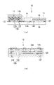
本実施形態の複合型電子部品10は、例えば図1の(a)、(b)に示すように、多層配線ブロック11と、第1のチップ型電子部品12Aを内蔵するチップ型電子部品内蔵多層ブロック12と、第2のチップ型電子部品13と、これら三者11、12、13が実装されてこれら三者を支持する支持基板14と、支持基板14上で多層配線ブロック11、チップ型電子部品内蔵多層ブロック12及び第2のチップ型電子部品13の三者を被覆して一体化する樹脂部15と、を備え、多層配線ブロック11、チップ型電子部品内蔵多層ブロック12及び第2のチップ型電子部品13の三者は支持基板14上でその表面に形成された表面配線パターン14Aを介して互いに電気的に接続されている。
本実施形態の複合型電子部品10Dは、例えば図7に示すようにシールド電極及びビアホール導体を有する以外は上記実施形態に準じて構成されている。即ち、本実施形態の複合型電子部品10Dは、同図に示すように、多層配線ブロック11、チップ型電子部品内蔵多層ブロック12、第2のチップ型電子部品13及び支持基板14を備え、多層配線ブロック11、チップ型電子部品内蔵多層ブロック12及び第2チップ型電子部品13が支持基板14上でプリプレグシートからなる樹脂部15を介して一体化されている。樹脂部15の上面は平坦化されており、且つ、その上面にはシールド電極16が形成され、このシールド電極16と支持基板14は断面形状が例えば円形、楕円形状等に形成されたビアホール導体17によって電気的に接続されている。
本実施形態の複合型電子部品10Eは、図7に示す複合型電子部品10Dから支持基板14を除いた以外は複合型電子部品10Dと同様に構成されている。本実施形態の複合型電子部品10Eは、図8に示すように、例えば剥離可能な転写用シート上または転写用フィルム(図示せず)上に形成することができる。複合型電子部品10Eをマザーボード等の実装基板に実装する場合には、複合型電子部品10Eから転写用シートまたは転写用フィルムを剥離して実装基板上に実装する。即ち、例えば銅箔等の金属箔を転写用シート上に剥離可能に貼り付ける。そして、フォトリソグラフィ技術及びエッチング技術を用いて所定のパターンで表面配線パターン14Aを形成した後、この表面配線パターン14Aに合わせて、多層配線ブロック11、チップ型電子部品内蔵多層ブロック12及び第2のチップ型電子部品13を実装する。次いで、樹脂プリプレグシートを圧着して多層配線ブロック11、チップ型電子部品内蔵多層ブロック12及び第2のチップ型電子部品13を一体化することによって複合型電子部品10Eを得ることができる。つまり、複合型電子部品10Eにおいては、マザーボード等の実装基板への実装は、各ブロックの外部端子電極に直接接続された配線パターン14Aによって行われる。
本実施形態においても上記各実施形態と同一または相当部分には同一符号を付して本実施形態について説明する。
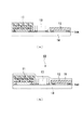
本実施形態の複合型電子部品10Fは、図9の(a)、(b)に示すように、多層配線ブロック11、チップ型電子部品内蔵多層ブロック12及び第2のチップ型電子部品13と、を備え、これら多層配線ブロック11及びチップ型電子部品内蔵多層ブロック12の絶縁層がそれぞれ熱硬化性樹脂によって形成されている。多層配線ブロック11、チップ型電子部品内蔵多層ブロック12及び第2のチップ型電子部品13は、いずれも下面に外部端子電極11E、12F、13Aが形成され、上記各実施形態に用いられたものに準じた構成を有している。本実施形態では第2のチップ型電子部品13は予め熱硬化性樹脂18Aによって封止されてブロック状を呈するチップ型電子部品ブロック18として構成されている。そして、本実施形態の複合型電子部品10Fは、同図の(b)に示すように、それぞれ同一高さに形成された多層配線ブロック11、チップ型電子部品内蔵多層ブロック12及びチップ型電子部品ブロック18がそれぞれ第1、第2樹脂ブロック19、20を介して電気的に接続されて一体化している。第1、第2樹脂ブロック19、20も他のブロックと同一高さに形成されている。
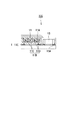
本実施形態の複合型電子部品10Jは、図13に示すように、高さ、幅、長さがそれぞれ略同一大きさに形成された多層配線ブロック11、チップ型電子部品内蔵多層ブロック12、チップ型電子部品ブロック18、及び隣接するブロックを電気的、機械的に接続する樹脂ブロック21を備え、これらのブロックが目的に応じた配列で配置されて全体として矩形状に形成されている。
本実施形態の複合型電子部品10Kは、図14に示すに示すように、多層配線ブロック11、チップ型電子部品内蔵多層ブロック12及びチップ型電子部品ブロック18のいずれか2つが同一大きさに形成され、他の一つがその略倍の面積を持つ大きさに形成されて、全体として矩形状を呈している。そして、これらのブロック11、12、18が樹脂ブロック22を介して互いに電気的、機械的に接続されて一体化している。
Claims (5)
- 複数の絶縁層が積層され且つ配線パターンを有する多層配線ブロック、複数の絶縁層が積層され且つ配線パターンを有すると共に第1のチップ型電子部品を内蔵するチップ型電子部品内蔵多層ブロック、及び受動部品または能動部品からなる第2のチップ型電子部品が樹脂封止されたチップ型電子部品ブロックの少なくともいずれか2つを備え、上記多層配線ブロック、上記チップ型電子部品内蔵型多層ブロック、及び第2のチップ型電子部品が樹脂封止されたチップ型電子部品ブロックの少なくともいずれか2つは、接続用配線を有する樹脂ブロックを介して互いに電気的に接続されて一体化して同一平面上に配置されていることを特徴とする複合型電子部品。
- 上記多層配線ブロック、上記チップ型電子部品内蔵多層ブロック、及び上記チップ型電子部品ブロックは、上記樹脂ブロックを介して一体化していることを特徴とする請求項1に記載の複合型電子部品。
- 上記多層配線ブロックと上記チップ型電子部品内蔵多層ブロックとは、互いに異なる材料で形成されていることを特徴とする請求項1または請求項2に記載の複合型電子部品。
- 複数の絶縁層が積層され且つ配線パターンを有する多層配線ブロック、複数の絶縁層が積層され且つ配線パターンを有すると共に第1のチップ型電子部品を内蔵するチップ型電子部品内蔵多層ブロック、及び第2のチップ型電子部品が樹脂封止されたチップ型電子部品ブロックの少なくともいずれか2つと、配線パターンを有する樹脂ブロックと、をそれぞれ同一平面上に配置する工程と、上記多層配線ブロック、上記チップ型電子部品内蔵多層ブロック、及び上記チップ型電子部品ブロックの少なくともいずれか2つを、上記樹脂ブロックを介して互いに圧着して電気的に接続する工程と、を備えたことを特徴とする複合型電子部品の製造方法。
- 上記多層配線ブロック、上記チップ型電子部品内蔵多層ブロック、上記チップ型電子部品ブロック、及び上記樹脂ブロックをそれぞれ配置する工程と、上記多層配線ブロック、上記チップ型電子部品内蔵多層ブロック、及び上記チップ型電子部品ブロックを、上記樹脂ブロックを介して互いに圧着して電気的に接続する工程と、を備えたことを特徴とする請求項4に記載の複合型電子部品の製造方法。
Applications Claiming Priority (5)
| Application Number | Priority Date | Filing Date | Title |
|---|---|---|---|
| JP2004224922 | 2004-07-30 | ||
| JP2004224922 | 2004-07-30 | ||
| JPPCT/JP2005/011358 | 2005-06-21 | ||
| PCT/JP2005/011358 WO2006011320A1 (ja) | 2004-07-30 | 2005-06-21 | 複合型電子部品及びその製造方法 |
| PCT/JP2005/013724 WO2006011508A1 (ja) | 2004-07-30 | 2005-07-27 | 複合型電子部品及びその製造方法 |
Publications (2)
| Publication Number | Publication Date |
|---|---|
| JPWO2006011508A1 JPWO2006011508A1 (ja) | 2008-05-01 |
| JP4453702B2 true JP4453702B2 (ja) | 2010-04-21 |
Family
ID=35786072
Family Applications (1)
| Application Number | Title | Priority Date | Filing Date |
|---|---|---|---|
| JP2006527819A Expired - Fee Related JP4453702B2 (ja) | 2004-07-30 | 2005-07-27 | 複合型電子部品及びその製造方法 |
Country Status (5)
| Country | Link |
|---|---|
| US (3) | US7684207B2 (ja) |
| JP (1) | JP4453702B2 (ja) |
| CN (1) | CN100556234C (ja) |
| AT (1) | ATE535138T1 (ja) |
| WO (1) | WO2006011320A1 (ja) |
Families Citing this family (25)
| Publication number | Priority date | Publication date | Assignee | Title |
|---|---|---|---|---|
| EP1699277A4 (en) * | 2003-12-26 | 2007-08-15 | Murata Manufacturing Co | CERAMIC MULTILAYER SUBSTRATE |
| JP2007266544A (ja) * | 2006-03-30 | 2007-10-11 | Koa Corp | 複合電子部品の製造法および複合電子部品 |
| JP5167671B2 (ja) * | 2006-10-31 | 2013-03-21 | ソニー株式会社 | 半導体素子 |
| EP2141972B1 (en) * | 2007-05-02 | 2014-04-02 | Murata Manufacturing Co. Ltd. | Component-incorporating module and its manufacturing method |
| US20080298023A1 (en) * | 2007-05-28 | 2008-12-04 | Matsushita Electric Industrial Co., Ltd. | Electronic component-containing module and manufacturing method thereof |
| WO2008155957A1 (ja) * | 2007-06-19 | 2008-12-24 | Murata Manufacturing Co., Ltd. | 部品内蔵基板の製造方法および部品内蔵基板 |
| CN101690434B (zh) * | 2007-06-26 | 2011-08-17 | 株式会社村田制作所 | 元器件内置基板的制造方法 |
| TWI363585B (en) * | 2008-04-02 | 2012-05-01 | Advanced Semiconductor Eng | Method for manufacturing a substrate having embedded component therein |
| US20100139967A1 (en) * | 2008-12-08 | 2010-06-10 | Ibiden Co., Ltd. | Wiring board and fabrication method therefor |
| KR101038234B1 (ko) * | 2009-02-24 | 2011-06-01 | 삼성전기주식회사 | 전자기 밴드갭 구조를 이용한 emi 노이즈 저감 기판 |
| TWI456715B (zh) * | 2009-06-19 | 2014-10-11 | Advanced Semiconductor Eng | 晶片封裝結構及其製造方法 |
| TWI392066B (zh) * | 2009-12-28 | 2013-04-01 | 矽品精密工業股份有限公司 | 封裝結構及其製法 |
| AT12737U1 (de) * | 2010-09-17 | 2012-10-15 | Austria Tech & System Tech | Verfahren zum herstellen einer aus mehreren leiterplattenbereichen bestehenden leiterplatte sowie leiterplatte |
| JP5737478B2 (ja) * | 2012-07-05 | 2015-06-17 | 株式会社村田製作所 | 部品内蔵基板 |
| JP6151724B2 (ja) * | 2013-01-30 | 2017-06-21 | 京セラ株式会社 | 実装構造体の製造方法 |
| US9190389B2 (en) | 2013-07-26 | 2015-11-17 | Infineon Technologies Ag | Chip package with passives |
| US9070568B2 (en) * | 2013-07-26 | 2015-06-30 | Infineon Technologies Ag | Chip package with embedded passive component |
| KR101666757B1 (ko) * | 2015-07-13 | 2016-10-24 | 앰코 테크놀로지 코리아 주식회사 | 반도체 패키지 |
| CN105451434B (zh) * | 2015-12-24 | 2018-03-27 | 广东欧珀移动通信有限公司 | 电路板、终端及电路板制作方法 |
| JP6191808B1 (ja) * | 2016-04-20 | 2017-09-06 | 株式会社村田製作所 | 多層基板および電子機器 |
| CN109892023B (zh) * | 2016-10-25 | 2022-03-22 | 株式会社村田制作所 | 电路模块 |
| WO2020189560A1 (ja) * | 2019-03-15 | 2020-09-24 | 株式会社村田製作所 | モジュール |
| US11289453B2 (en) | 2020-02-27 | 2022-03-29 | Qualcomm Incorporated | Package comprising a substrate and a high-density interconnect structure coupled to the substrate |
| US11605594B2 (en) * | 2020-03-23 | 2023-03-14 | Qualcomm Incorporated | Package comprising a substrate and a high-density interconnect integrated device coupled to the substrate |
| CN112071811A (zh) * | 2020-09-18 | 2020-12-11 | 环维电子(上海)有限公司 | 半导体封装件及其制作方法 |
Family Cites Families (22)
| Publication number | Priority date | Publication date | Assignee | Title |
|---|---|---|---|---|
| US4635356A (en) * | 1984-12-28 | 1987-01-13 | Kabushiki Kaisha Toshiba | Method of manufacturing a circuit module |
| US5111278A (en) * | 1991-03-27 | 1992-05-05 | Eichelberger Charles W | Three-dimensional multichip module systems |
| JP3229525B2 (ja) * | 1995-07-26 | 2001-11-19 | 株式会社日立製作所 | Lsi内蔵型多層回路板およびその製法 |
| US6038133A (en) | 1997-11-25 | 2000-03-14 | Matsushita Electric Industrial Co., Ltd. | Circuit component built-in module and method for producing the same |
| JP3375555B2 (ja) | 1997-11-25 | 2003-02-10 | 松下電器産業株式会社 | 回路部品内蔵モジュールおよびその製造方法 |
| US6370013B1 (en) * | 1999-11-30 | 2002-04-09 | Kyocera Corporation | Electric element incorporating wiring board |
| JP3547423B2 (ja) | 2000-12-27 | 2004-07-28 | 松下電器産業株式会社 | 部品内蔵モジュール及びその製造方法 |
| JP3553043B2 (ja) | 2001-01-19 | 2004-08-11 | 松下電器産業株式会社 | 部品内蔵モジュールとその製造方法 |
| DE10295940B4 (de) * | 2001-01-31 | 2013-04-04 | Sony Corp. | Verfahren zur Herstellung einer Halbleitereinrichtung mit einem plattenförmigen Schaltungsblock |
| JP2002271038A (ja) | 2001-03-12 | 2002-09-20 | Matsushita Electric Ind Co Ltd | 複合多層基板およびその製造方法ならびに電子部品 |
| MXPA02005829A (es) * | 2001-06-13 | 2004-12-13 | Denso Corp | Tablero de cableados impresos con dispositivo electrico incrustado y metodo para la manufactura de tablero de cableados impresos con dispositivo electrico incrustado. |
| JP2003100937A (ja) | 2001-09-26 | 2003-04-04 | Hitachi Ltd | 高周波モジュール |
| TW550997B (en) * | 2001-10-18 | 2003-09-01 | Matsushita Electric Ind Co Ltd | Module with built-in components and the manufacturing method thereof |
| JP2003163459A (ja) | 2001-11-26 | 2003-06-06 | Sony Corp | 高周波回路ブロック体及びその製造方法、高周波モジュール装置及びその製造方法。 |
| JP2003188338A (ja) * | 2001-12-13 | 2003-07-04 | Sony Corp | 回路基板装置及びその製造方法 |
| TW200302685A (en) * | 2002-01-23 | 2003-08-01 | Matsushita Electric Ind Co Ltd | Circuit component built-in module and method of manufacturing the same |
| JP2003249763A (ja) * | 2002-02-25 | 2003-09-05 | Fujitsu Ltd | 多層配線基板及びその製造方法 |
| JP2003249510A (ja) | 2002-02-26 | 2003-09-05 | Asuriito Fa Kk | 半導体封止方法 |
| JP2004056155A (ja) * | 2002-07-19 | 2004-02-19 | Matsushita Electric Ind Co Ltd | モジュール部品 |
| EP1416532A4 (en) | 2002-07-19 | 2005-08-17 | Matsushita Electric Ind Co Ltd | MODULE COMPONENT |
| JP4178880B2 (ja) * | 2002-08-29 | 2008-11-12 | 松下電器産業株式会社 | モジュール部品 |
| JP4552524B2 (ja) * | 2004-06-10 | 2010-09-29 | パナソニック株式会社 | 複合型電子部品 |
-
2005
- 2005-06-21 WO PCT/JP2005/011358 patent/WO2006011320A1/ja active Application Filing
- 2005-07-27 JP JP2006527819A patent/JP4453702B2/ja not_active Expired - Fee Related
- 2005-07-27 AT AT05780155T patent/ATE535138T1/de active
- 2005-07-27 CN CNB2005800210761A patent/CN100556234C/zh active Active
-
2006
- 2006-12-13 US US11/609,989 patent/US7684207B2/en active Active
-
2007
- 2007-03-27 US US11/691,666 patent/US7594316B2/en active Active
-
2010
- 2010-02-01 US US12/697,451 patent/US7929316B2/en active Active
Also Published As
| Publication number | Publication date |
|---|---|
| US7929316B2 (en) | 2011-04-19 |
| CN1973587A (zh) | 2007-05-30 |
| CN100556234C (zh) | 2009-10-28 |
| US7594316B2 (en) | 2009-09-29 |
| ATE535138T1 (de) | 2011-12-15 |
| US20100134990A1 (en) | 2010-06-03 |
| US7684207B2 (en) | 2010-03-23 |
| US20070081312A1 (en) | 2007-04-12 |
| US20070188998A1 (en) | 2007-08-16 |
| WO2006011320A1 (ja) | 2006-02-02 |
| JPWO2006011508A1 (ja) | 2008-05-01 |
Similar Documents
| Publication | Publication Date | Title |
|---|---|---|
| JP4453702B2 (ja) | 複合型電子部品及びその製造方法 | |
| JP4310467B2 (ja) | 複合多層基板及びその製造方法 | |
| JP3709882B2 (ja) | 回路モジュールとその製造方法 | |
| JP4367414B2 (ja) | 部品内蔵モジュールおよびその製造方法 | |
| JP4111239B2 (ja) | 複合セラミック基板 | |
| JP4329884B2 (ja) | 部品内蔵モジュール | |
| WO2005067359A1 (ja) | セラミック多層基板 | |
| EP1776002B1 (en) | Composite electronic component and method for manufacturing the same | |
| JP4821424B2 (ja) | セラミック多層基板及びその製造方法 | |
| JP4158798B2 (ja) | 複合セラミック基板 | |
| JP4160923B2 (ja) | 電子部品 | |
| JP2006128229A (ja) | 複合多層基板 | |
| JP2004056115A (ja) | 多層配線基板 | |
| JP2005235807A (ja) | 積層型電子部品およびその製造方法 | |
| JP4403820B2 (ja) | 積層型電子部品およびその製造方法 | |
| WO2005101934A1 (ja) | 複合型電子部品及びその製造方法 | |
| KR100828925B1 (ko) | 복합형 전자부품 및 그 제조방법 | |
| JP2007305631A (ja) | 樹脂多層基板、複合型電子部品及びそれぞれの製造方法 | |
| WO2013099360A1 (ja) | モジュールおよびこれを備えるモジュール搭載部品 | |
| JP2008135483A (ja) | 電子部品内蔵基板およびその製造方法 | |
| JP4558004B2 (ja) | 電子部品、シールドカバー、多数個取り用母基板、配線基板及び電子機器 | |
| JP4276284B2 (ja) | 電子部品の製造方法および電子部品用母基板 | |
| JP4511513B2 (ja) | 電子部品及びその製造方法 | |
| JP4511573B2 (ja) | 電子部品およびこれを備えた電子機器 | |
| JP4558058B2 (ja) | 電子部品 |
Legal Events
| Date | Code | Title | Description |
|---|---|---|---|
| A131 | Notification of reasons for refusal |
Free format text: JAPANESE INTERMEDIATE CODE: A131 Effective date: 20090818 |
|
| A521 | Request for written amendment filed |
Free format text: JAPANESE INTERMEDIATE CODE: A523 Effective date: 20091015 |
|
| TRDD | Decision of grant or rejection written | ||
| A01 | Written decision to grant a patent or to grant a registration (utility model) |
Free format text: JAPANESE INTERMEDIATE CODE: A01 Effective date: 20100112 |
|
| A01 | Written decision to grant a patent or to grant a registration (utility model) |
Free format text: JAPANESE INTERMEDIATE CODE: A01 |
|
| A61 | First payment of annual fees (during grant procedure) |
Free format text: JAPANESE INTERMEDIATE CODE: A61 Effective date: 20100125 |
|
| FPAY | Renewal fee payment (event date is renewal date of database) |
Free format text: PAYMENT UNTIL: 20130212 Year of fee payment: 3 |
|
| R150 | Certificate of patent or registration of utility model |
Free format text: JAPANESE INTERMEDIATE CODE: R150 |
|
| LAPS | Cancellation because of no payment of annual fees |