JP3896112B2 - 半導体集積回路装置 - Google Patents
半導体集積回路装置 Download PDFInfo
- Publication number
- JP3896112B2 JP3896112B2 JP2003428888A JP2003428888A JP3896112B2 JP 3896112 B2 JP3896112 B2 JP 3896112B2 JP 2003428888 A JP2003428888 A JP 2003428888A JP 2003428888 A JP2003428888 A JP 2003428888A JP 3896112 B2 JP3896112 B2 JP 3896112B2
- Authority
- JP
- Japan
- Prior art keywords
- dram
- integrated circuit
- interposer
- semiconductor integrated
- circuit device
- Prior art date
- Legal status (The legal status is an assumption and is not a legal conclusion. Google has not performed a legal analysis and makes no representation as to the accuracy of the status listed.)
- Expired - Fee Related
Links
Images


Classifications
-
- H—ELECTRICITY
- H01—ELECTRIC ELEMENTS
- H01L—SEMICONDUCTOR DEVICES NOT COVERED BY CLASS H10
- H01L23/00—Details of semiconductor or other solid state devices
- H01L23/58—Structural electrical arrangements for semiconductor devices not otherwise provided for, e.g. in combination with batteries
- H01L23/64—Impedance arrangements
- H01L23/66—High-frequency adaptations
-
- G—PHYSICS
- G06—COMPUTING OR CALCULATING; COUNTING
- G06F—ELECTRIC DIGITAL DATA PROCESSING
- G06F1/00—Details not covered by groups G06F3/00 - G06F13/00 and G06F21/00
- G06F1/16—Constructional details or arrangements
- G06F1/18—Packaging or power distribution
- G06F1/183—Internal mounting support structures, e.g. for printed circuit boards, internal connecting means
- G06F1/184—Mounting of motherboards
-
- G—PHYSICS
- G06—COMPUTING OR CALCULATING; COUNTING
- G06F—ELECTRIC DIGITAL DATA PROCESSING
- G06F1/00—Details not covered by groups G06F3/00 - G06F13/00 and G06F21/00
- G06F1/16—Constructional details or arrangements
- G06F1/18—Packaging or power distribution
- G06F1/183—Internal mounting support structures, e.g. for printed circuit boards, internal connecting means
- G06F1/185—Mounting of expansion boards
-
- G—PHYSICS
- G06—COMPUTING OR CALCULATING; COUNTING
- G06F—ELECTRIC DIGITAL DATA PROCESSING
- G06F1/00—Details not covered by groups G06F3/00 - G06F13/00 and G06F21/00
- G06F1/16—Constructional details or arrangements
- G06F1/18—Packaging or power distribution
- G06F1/183—Internal mounting support structures, e.g. for printed circuit boards, internal connecting means
- G06F1/186—Securing of expansion boards in correspondence to slots provided at the computer enclosure
-
- G—PHYSICS
- G11—INFORMATION STORAGE
- G11C—STATIC STORES
- G11C5/00—Details of stores covered by group G11C11/00
- G11C5/02—Disposition of storage elements, e.g. in the form of a matrix array
- G11C5/025—Geometric lay-out considerations of storage- and peripheral-blocks in a semiconductor storage device
-
- H—ELECTRICITY
- H01—ELECTRIC ELEMENTS
- H01L—SEMICONDUCTOR DEVICES NOT COVERED BY CLASS H10
- H01L21/00—Processes or apparatus adapted for the manufacture or treatment of semiconductor or solid state devices or of parts thereof
- H01L21/67—Apparatus specially adapted for handling semiconductor or electric solid state devices during manufacture or treatment thereof; Apparatus specially adapted for handling wafers during manufacture or treatment of semiconductor or electric solid state devices or components ; Apparatus not specifically provided for elsewhere
- H01L21/683—Apparatus specially adapted for handling semiconductor or electric solid state devices during manufacture or treatment thereof; Apparatus specially adapted for handling wafers during manufacture or treatment of semiconductor or electric solid state devices or components ; Apparatus not specifically provided for elsewhere for supporting or gripping
- H01L21/6835—Apparatus specially adapted for handling semiconductor or electric solid state devices during manufacture or treatment thereof; Apparatus specially adapted for handling wafers during manufacture or treatment of semiconductor or electric solid state devices or components ; Apparatus not specifically provided for elsewhere for supporting or gripping using temporarily an auxiliary support
-
- H—ELECTRICITY
- H01—ELECTRIC ELEMENTS
- H01L—SEMICONDUCTOR DEVICES NOT COVERED BY CLASS H10
- H01L23/00—Details of semiconductor or other solid state devices
- H01L23/48—Arrangements for conducting electric current to or from the solid state body in operation, e.g. leads, terminal arrangements ; Selection of materials therefor
- H01L23/488—Arrangements for conducting electric current to or from the solid state body in operation, e.g. leads, terminal arrangements ; Selection of materials therefor consisting of soldered or bonded constructions
- H01L23/498—Leads, i.e. metallisations or lead-frames on insulating substrates, e.g. chip carriers
- H01L23/49822—Multilayer substrates
-
- H—ELECTRICITY
- H01—ELECTRIC ELEMENTS
- H01L—SEMICONDUCTOR DEVICES NOT COVERED BY CLASS H10
- H01L23/00—Details of semiconductor or other solid state devices
- H01L23/48—Arrangements for conducting electric current to or from the solid state body in operation, e.g. leads, terminal arrangements ; Selection of materials therefor
- H01L23/488—Arrangements for conducting electric current to or from the solid state body in operation, e.g. leads, terminal arrangements ; Selection of materials therefor consisting of soldered or bonded constructions
- H01L23/498—Leads, i.e. metallisations or lead-frames on insulating substrates, e.g. chip carriers
- H01L23/49833—Leads, i.e. metallisations or lead-frames on insulating substrates, e.g. chip carriers the chip support structure consisting of a plurality of insulating substrates
-
- H—ELECTRICITY
- H01—ELECTRIC ELEMENTS
- H01L—SEMICONDUCTOR DEVICES NOT COVERED BY CLASS H10
- H01L23/00—Details of semiconductor or other solid state devices
- H01L23/48—Arrangements for conducting electric current to or from the solid state body in operation, e.g. leads, terminal arrangements ; Selection of materials therefor
- H01L23/50—Arrangements for conducting electric current to or from the solid state body in operation, e.g. leads, terminal arrangements ; Selection of materials therefor for integrated circuit devices, e.g. power bus, number of leads
-
- H—ELECTRICITY
- H01—ELECTRIC ELEMENTS
- H01L—SEMICONDUCTOR DEVICES NOT COVERED BY CLASS H10
- H01L2221/00—Processes or apparatus adapted for the manufacture or treatment of semiconductor or solid state devices or of parts thereof covered by H01L21/00
- H01L2221/67—Apparatus for handling semiconductor or electric solid state devices during manufacture or treatment thereof; Apparatus for handling wafers during manufacture or treatment of semiconductor or electric solid state devices or components; Apparatus not specifically provided for elsewhere
- H01L2221/683—Apparatus for handling semiconductor or electric solid state devices during manufacture or treatment thereof; Apparatus for handling wafers during manufacture or treatment of semiconductor or electric solid state devices or components; Apparatus not specifically provided for elsewhere for supporting or gripping
- H01L2221/68304—Apparatus for handling semiconductor or electric solid state devices during manufacture or treatment thereof; Apparatus for handling wafers during manufacture or treatment of semiconductor or electric solid state devices or components; Apparatus not specifically provided for elsewhere for supporting or gripping using temporarily an auxiliary support
- H01L2221/6834—Apparatus for handling semiconductor or electric solid state devices during manufacture or treatment thereof; Apparatus for handling wafers during manufacture or treatment of semiconductor or electric solid state devices or components; Apparatus not specifically provided for elsewhere for supporting or gripping using temporarily an auxiliary support used to protect an active side of a device or wafer
-
- H—ELECTRICITY
- H01—ELECTRIC ELEMENTS
- H01L—SEMICONDUCTOR DEVICES NOT COVERED BY CLASS H10
- H01L2221/00—Processes or apparatus adapted for the manufacture or treatment of semiconductor or solid state devices or of parts thereof covered by H01L21/00
- H01L2221/67—Apparatus for handling semiconductor or electric solid state devices during manufacture or treatment thereof; Apparatus for handling wafers during manufacture or treatment of semiconductor or electric solid state devices or components; Apparatus not specifically provided for elsewhere
- H01L2221/683—Apparatus for handling semiconductor or electric solid state devices during manufacture or treatment thereof; Apparatus for handling wafers during manufacture or treatment of semiconductor or electric solid state devices or components; Apparatus not specifically provided for elsewhere for supporting or gripping
- H01L2221/68304—Apparatus for handling semiconductor or electric solid state devices during manufacture or treatment thereof; Apparatus for handling wafers during manufacture or treatment of semiconductor or electric solid state devices or components; Apparatus not specifically provided for elsewhere for supporting or gripping using temporarily an auxiliary support
- H01L2221/68368—Apparatus for handling semiconductor or electric solid state devices during manufacture or treatment thereof; Apparatus for handling wafers during manufacture or treatment of semiconductor or electric solid state devices or components; Apparatus not specifically provided for elsewhere for supporting or gripping using temporarily an auxiliary support used in a transfer process involving at least two transfer steps, i.e. including an intermediate handle substrate
-
- H—ELECTRICITY
- H01—ELECTRIC ELEMENTS
- H01L—SEMICONDUCTOR DEVICES NOT COVERED BY CLASS H10
- H01L2224/00—Indexing scheme for arrangements for connecting or disconnecting semiconductor or solid-state bodies and methods related thereto as covered by H01L24/00
- H01L2224/01—Means for bonding being attached to, or being formed on, the surface to be connected, e.g. chip-to-package, die-attach, "first-level" interconnects; Manufacturing methods related thereto
- H01L2224/10—Bump connectors; Manufacturing methods related thereto
- H01L2224/15—Structure, shape, material or disposition of the bump connectors after the connecting process
- H01L2224/16—Structure, shape, material or disposition of the bump connectors after the connecting process of an individual bump connector
-
- H—ELECTRICITY
- H01—ELECTRIC ELEMENTS
- H01L—SEMICONDUCTOR DEVICES NOT COVERED BY CLASS H10
- H01L2924/00—Indexing scheme for arrangements or methods for connecting or disconnecting semiconductor or solid-state bodies as covered by H01L24/00
- H01L2924/01—Chemical elements
- H01L2924/01004—Beryllium [Be]
-
- H—ELECTRICITY
- H01—ELECTRIC ELEMENTS
- H01L—SEMICONDUCTOR DEVICES NOT COVERED BY CLASS H10
- H01L2924/00—Indexing scheme for arrangements or methods for connecting or disconnecting semiconductor or solid-state bodies as covered by H01L24/00
- H01L2924/01—Chemical elements
- H01L2924/0102—Calcium [Ca]
-
- H—ELECTRICITY
- H01—ELECTRIC ELEMENTS
- H01L—SEMICONDUCTOR DEVICES NOT COVERED BY CLASS H10
- H01L2924/00—Indexing scheme for arrangements or methods for connecting or disconnecting semiconductor or solid-state bodies as covered by H01L24/00
- H01L2924/01—Chemical elements
- H01L2924/01068—Erbium [Er]
-
- H—ELECTRICITY
- H01—ELECTRIC ELEMENTS
- H01L—SEMICONDUCTOR DEVICES NOT COVERED BY CLASS H10
- H01L2924/00—Indexing scheme for arrangements or methods for connecting or disconnecting semiconductor or solid-state bodies as covered by H01L24/00
- H01L2924/10—Details of semiconductor or other solid state devices to be connected
- H01L2924/11—Device type
- H01L2924/13—Discrete devices, e.g. 3 terminal devices
- H01L2924/1304—Transistor
- H01L2924/1306—Field-effect transistor [FET]
- H01L2924/13091—Metal-Oxide-Semiconductor Field-Effect Transistor [MOSFET]
-
- H—ELECTRICITY
- H01—ELECTRIC ELEMENTS
- H01L—SEMICONDUCTOR DEVICES NOT COVERED BY CLASS H10
- H01L2924/00—Indexing scheme for arrangements or methods for connecting or disconnecting semiconductor or solid-state bodies as covered by H01L24/00
- H01L2924/15—Details of package parts other than the semiconductor or other solid state devices to be connected
- H01L2924/151—Die mounting substrate
- H01L2924/153—Connection portion
- H01L2924/1531—Connection portion the connection portion being formed only on the surface of the substrate opposite to the die mounting surface
- H01L2924/15311—Connection portion the connection portion being formed only on the surface of the substrate opposite to the die mounting surface being a ball array, e.g. BGA
-
- H—ELECTRICITY
- H01—ELECTRIC ELEMENTS
- H01L—SEMICONDUCTOR DEVICES NOT COVERED BY CLASS H10
- H01L2924/00—Indexing scheme for arrangements or methods for connecting or disconnecting semiconductor or solid-state bodies as covered by H01L24/00
- H01L2924/19—Details of hybrid assemblies other than the semiconductor or other solid state devices to be connected
- H01L2924/1901—Structure
- H01L2924/1904—Component type
- H01L2924/19041—Component type being a capacitor
-
- H—ELECTRICITY
- H01—ELECTRIC ELEMENTS
- H01L—SEMICONDUCTOR DEVICES NOT COVERED BY CLASS H10
- H01L2924/00—Indexing scheme for arrangements or methods for connecting or disconnecting semiconductor or solid-state bodies as covered by H01L24/00
- H01L2924/30—Technical effects
- H01L2924/301—Electrical effects
- H01L2924/30105—Capacitance
-
- H—ELECTRICITY
- H01—ELECTRIC ELEMENTS
- H01L—SEMICONDUCTOR DEVICES NOT COVERED BY CLASS H10
- H01L2924/00—Indexing scheme for arrangements or methods for connecting or disconnecting semiconductor or solid-state bodies as covered by H01L24/00
- H01L2924/30—Technical effects
- H01L2924/301—Electrical effects
- H01L2924/3011—Impedance
-
- H—ELECTRICITY
- H05—ELECTRIC TECHNIQUES NOT OTHERWISE PROVIDED FOR
- H05K—PRINTED CIRCUITS; CASINGS OR CONSTRUCTIONAL DETAILS OF ELECTRIC APPARATUS; MANUFACTURE OF ASSEMBLAGES OF ELECTRICAL COMPONENTS
- H05K1/00—Printed circuits
- H05K1/02—Details
- H05K1/14—Structural association of two or more printed circuits
- H05K1/141—One or more single auxiliary printed circuits mounted on a main printed circuit, e.g. modules, adapters
Landscapes
- Engineering & Computer Science (AREA)
- Computer Hardware Design (AREA)
- Power Engineering (AREA)
- Physics & Mathematics (AREA)
- General Physics & Mathematics (AREA)
- Theoretical Computer Science (AREA)
- Microelectronics & Electronic Packaging (AREA)
- Condensed Matter Physics & Semiconductors (AREA)
- General Engineering & Computer Science (AREA)
- Human Computer Interaction (AREA)
- Manufacturing & Machinery (AREA)
- Dram (AREA)
- Semiconductor Memories (AREA)
- Internal Circuitry In Semiconductor Integrated Circuit Devices (AREA)
- Memory System (AREA)
- Semiconductor Integrated Circuits (AREA)
Description
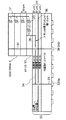
2a,2b,92,94−1,94−2 バッファ
3a,3b,6−1,6−2,70,91−1,91−2 DRAMチップ
4,102,103,143,230,240 チップセット
5,142,233 マザーボード
6,6a,6b,140,140a,140b,231,241d COC DRAM
7a,7b,141,141a,141b,264 インタポーザ
8,8a,8b Si基板部
9,9a,9b,31 絶縁層部
10,10a,10b、30 Si(シリコン)部
11,11a,11b,191a,191b PCB部
12,12a,12b,90,256 I/F LSI
14a,14b,100a,100b,144a,144a1,144a8,144b,144b1,144b8,193a,193a1,193a8,193b,193b1,193b8,234a,234a1,234a2,234b,234c,234d,234d1,234d2,244a,244a1,244a2,244b,244c,244d,244d1,244d2 DRAM積層体
15a,15b,34,42,45,150,151 配線
16,16a,16b,38 GNDレファレンスプレーン
17,17a,17b,17−1,17−1a,17−2,17−2a,22,26,33,35,37,43,48,52,53,56,76,85,86,246a,252,258,259,262,263 貫通電極
20,24,40,44,46,50,54,59,75,77,160,161,162,163 半田ボール
21,25,41,47,51,55,60 ビア
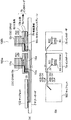
23 論理回路
32,36 フリップチップ電極
49 GNDレファレンス線
57 VDDプレーン
58 VDD線
71 メモリセルアレイ
72 周辺回路領域
73 チップ周辺領域
78 カップリングコンデンサ
80 小型高周波コネクタ
85、86 信号群
93−1,93−2 CLK分配回路
95−1,95−2 フリップフロップ群
130 端子
190,190a,190b,232,242 Siインタポーザ兼I/F LSI
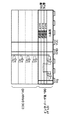
250 支持体
251 接着物
253−1,253−2,253−3,253−4 DRAMコア
254 貫通電極端子
257 フリップチップ接続端子
260 貫通電極端子
Claims (19)
- チップセットが搭載されたマザーボードと、当該マザーボードに実装され、かつ前記チップセットに接続されるメモリ部とを備える半導体集積回路装置において、
前記メモリ部として複数のDRAMチップを互いに積層した積層DRAMを用い、
前記積層DRAMを前記マザーボードに実装するためにインタポーザを用い、
当該前記インタポーザは、前記積層DRAMと前記チップセットとを電気的に接続する配線を含むシリコン部と、当該シリコン部の下側に設けられた当該シリコン部と実質上同じサイズの印刷回路基板とを有し、
当該印刷回路基板に前記配線に対して電位基準を与えるレファレンスプレーンが設けられていることを特徴とする半導体集積回路装置。 - 請求項1に記載の半導体集積回路装置において、
前記積層DRAMと前記インタポーザとの間に前記積層DRAMと前記チップセットとの間の信号授受を仲介するインタフェースLSIをさらに備え、
該インタフェースLSIと前記チップセットとが、前記インタポーザ及び前記マザーボードを介してポイント・トゥ・ポイント接続されていることを特徴とする半導体集積回路装置。 - 請求項2に記載の半導体集積回路装置において、
前記積層DRAM、前記インタフェースLSI及び前記インタポーザからなる組を複数備え、
互いに隣接する組同士が前記マザーボードを介してポイント・トゥ・ポイント接続されていることを特徴とする半導体集積回路装置。 - 請求項1、2または3に記載の半導体集積回路装置において、
前記印刷回路基板と前記マザーボードとが同軸タイプのコネクタで接続されていることを特徴とする半導体集積回路装置。 - 請求項2に記載の半導体集積回路装置において、
前記インタフェースLSIが貫通電極を有し、かつフェースアップであることを特徴とする半導体集積回路装置。 - 請求項2記載の半導体集積回路装置において、
前記積層DRAMに必要とされる共通論理回路を前記インタフェースLSIに設けたことを特徴とする半導体集積回路装置。 - 請求項1に記載の半導体集積回路装置において、
前記積層DRAMと前記インタポーザとの組を複数備え、
これら複数の組が前記チップセットにポイント・トゥ・ポイント接続又は共通接続されていることを特徴とする半導体集積回路装置。 - 請求項7に記載の半導体集積回路装置において、
前記積層DRAMと前記チップセットとの間で授受される信号の前記インタポーザが備える入出力端子への割り振りを、同一属性の信号毎に、前記積層DRAMの中心軸を中心とする同心円状に行うようにしたことを特徴とする半導体集積回路装置。 - 請求項1に記載の半導体集積回路装置において、
前記積層DRAM及び前記インタポーザからなる組を複数備え、
これら複数の組が前記チップセットにフライ・バイ接続されるように、コマンドアドレス信号用メインバスとデータ信号用メインバスとが、各組の直下で直交するよう前記マザーボードに設けられ、
前記コマンドアドレス信号用メインバス及びデータ信号用メインバスのそれぞれから各組の前記積層DRAMまでのスタブ長が2mm以下にされている、
ことを特徴とする半導体集積回路装置。 - 請求項1に記載の半導体集積回路装置において、
前記インタポーザが、前記集積DRAMと前記チップセットとの間の信号の授受を仲介するSiインタポーザ兼インタフェースLSIであることを特徴とする半導体集積回路装置。 - 請求項10に記載の半導体集積回路装置において、
前記積層DRAM及び前記Siインタポーザ兼インタフェースLSIからなる組を複数備え、
これら複数の組が行列配置され、前記チップセットにフライ・バイ接続されるように、コマンドアドレス信号用メインバスとデータ信号用メインバスとが、各組が搭載される領域において直交するよう前記マザーボードに格子状に設けられている、
ことを特徴とする半導体集積回路装置。 - 請求項10に記載の半導体集積回路装置において、
前記積層DRAM及び前記Siインタポーザ兼インタフェースLSIからなる組を複数備え、
これら複数の組が行列配置され、前記チップセットにフライ・バイ接続されるように、コマンドアドレス信号用メインバスとデータ信号用メインバスとが、各組の直下で平行となるよう前記マザーボードに平行に設けられている、
ことを特徴とする半導体集積回路装置。 - 請求項10に記載の半導体集積回路装置において、
前記積層DRAM及び前記Siインタポーザ兼インタフェースLSIからなる組を複数備え、
これら複数の組が行列配置され、前記チップセットにもっとも近い行に属する組はそれぞれ前記チップセットにポイント・トゥ・ポイント接続され、
残りの行に属する組は、各列毎に、互いに隣り合う組とポイント・トゥ・ポイント接続されている、
ことを特徴とする半導体集積回路装置。 - 請求項10乃至13のいずれか一つに記載の半導体集積回路装置において、
積層DRAMとSiインタポーザ兼インタフェースLSIの平面サイズが実質上同一である、
ことを特徴とする半導体集積回路装置。 - 請求項10乃至14のいずれか一つに記載の半導体集積回路装置において、
Siインタポーザ兼インタフェースLSIが貫通電極を備えていない、
ことを特徴とする半導体集積回路装置。 - 請求項15に記載の半導体集積回路装置において、
複数のDRAMチップを積層して前記積層DRAMを作成する際に、前記Siインタポーザ兼インタフェースLSIを支持体として利用するようにした、
ことを特徴とする半導体集積回路装置。 - 請求項1乃至16のいずれかに記載の半導体集積回路装置において、
前記積層DRAMが貫通電極を有し、当該貫通電極が前記複数のDRAMチップにおける周辺回路領域に設けられていることを特徴とする半導体集積回路装置。 - 請求項2,3,5,6,及び10乃至16のいずれかに記載の半導体集積回路装置において、
前記インタフェースLSI又は前記Siインタポーザ兼インタフェースLSIと前記積層DRAMとの間の接続が無終端接続により行われている、
ことを特徴とする半導体集積回路装置。 - 請求項1乃至14のいずれか一つに記載の半導体集積回路装置において、前記インタポーザの上面に電源線と接地線との間に接続されたデカップリングコンデンサを備える、
ことを特徴とする半導体集積回路装置。
Priority Applications (6)
| Application Number | Priority Date | Filing Date | Title |
|---|---|---|---|
| JP2003428888A JP3896112B2 (ja) | 2003-12-25 | 2003-12-25 | 半導体集積回路装置 |
| DE102004062194A DE102004062194A1 (de) | 2003-12-25 | 2004-12-23 | Integrierte Halbleiterschaltungs-Vorrichtung |
| US11/019,553 US7385281B2 (en) | 2003-12-25 | 2004-12-23 | Semiconductor integrated circuit device |
| CN200810170330.XA CN101419966A (zh) | 2003-12-25 | 2004-12-24 | 半导体集成电路装置 |
| CNB2004100615407A CN100442503C (zh) | 2003-12-25 | 2004-12-24 | 半导体集成电路装置 |
| US12/113,414 US8064222B2 (en) | 2003-12-25 | 2008-05-01 | Semiconductor integrated circuit device |
Applications Claiming Priority (1)
| Application Number | Priority Date | Filing Date | Title |
|---|---|---|---|
| JP2003428888A JP3896112B2 (ja) | 2003-12-25 | 2003-12-25 | 半導体集積回路装置 |
Publications (2)
| Publication Number | Publication Date |
|---|---|
| JP2005191172A JP2005191172A (ja) | 2005-07-14 |
| JP3896112B2 true JP3896112B2 (ja) | 2007-03-22 |
Family
ID=34697542
Family Applications (1)
| Application Number | Title | Priority Date | Filing Date |
|---|---|---|---|
| JP2003428888A Expired - Fee Related JP3896112B2 (ja) | 2003-12-25 | 2003-12-25 | 半導体集積回路装置 |
Country Status (4)
| Country | Link |
|---|---|
| US (2) | US7385281B2 (ja) |
| JP (1) | JP3896112B2 (ja) |
| CN (2) | CN100442503C (ja) |
| DE (1) | DE102004062194A1 (ja) |
Cited By (1)
| Publication number | Priority date | Publication date | Assignee | Title |
|---|---|---|---|---|
| US10820419B2 (en) | 2018-05-30 | 2020-10-27 | Samsung Electronics Co., Ltd. | Memory system and storage device including printed circuit board where channel groups have both point to point topology and daisy chain topology |
Families Citing this family (106)
| Publication number | Priority date | Publication date | Assignee | Title |
|---|---|---|---|---|
| JP4745697B2 (ja) * | 2005-03-29 | 2011-08-10 | 富士通セミコンダクター株式会社 | 複数の配線層を有する半導体回路の端子層設定方法、端子層設定プログラム、配線端子延長処理プログラム、および、その端子層を設定に用いられる端子延長用コンポーネント |
| US8244971B2 (en) | 2006-07-31 | 2012-08-14 | Google Inc. | Memory circuit system and method |
| US9507739B2 (en) | 2005-06-24 | 2016-11-29 | Google Inc. | Configurable memory circuit system and method |
| US8359187B2 (en) | 2005-06-24 | 2013-01-22 | Google Inc. | Simulating a different number of memory circuit devices |
| US7590796B2 (en) | 2006-07-31 | 2009-09-15 | Metaram, Inc. | System and method for power management in memory systems |
| US20080082763A1 (en) | 2006-10-02 | 2008-04-03 | Metaram, Inc. | Apparatus and method for power management of memory circuits by a system or component thereof |
| WO2007002324A2 (en) | 2005-06-24 | 2007-01-04 | Metaram, Inc. | An integrated memory core and memory interface circuit |
| US8386722B1 (en) | 2008-06-23 | 2013-02-26 | Google Inc. | Stacked DIMM memory interface |
| US10013371B2 (en) | 2005-06-24 | 2018-07-03 | Google Llc | Configurable memory circuit system and method |
| US8089795B2 (en) | 2006-02-09 | 2012-01-03 | Google Inc. | Memory module with memory stack and interface with enhanced capabilities |
| US8397013B1 (en) | 2006-10-05 | 2013-03-12 | Google Inc. | Hybrid memory module |
| US8438328B2 (en) * | 2008-02-21 | 2013-05-07 | Google Inc. | Emulation of abstracted DIMMs using abstracted DRAMs |
| US8041881B2 (en) | 2006-07-31 | 2011-10-18 | Google Inc. | Memory device with emulated characteristics |
| US8055833B2 (en) | 2006-10-05 | 2011-11-08 | Google Inc. | System and method for increasing capacity, performance, and flexibility of flash storage |
| US7580312B2 (en) | 2006-07-31 | 2009-08-25 | Metaram, Inc. | Power saving system and method for use with a plurality of memory circuits |
| US8111566B1 (en) | 2007-11-16 | 2012-02-07 | Google, Inc. | Optimal channel design for memory devices for providing a high-speed memory interface |
| US9171585B2 (en) | 2005-06-24 | 2015-10-27 | Google Inc. | Configurable memory circuit system and method |
| US8090897B2 (en) | 2006-07-31 | 2012-01-03 | Google Inc. | System and method for simulating an aspect of a memory circuit |
| US8060774B2 (en) | 2005-06-24 | 2011-11-15 | Google Inc. | Memory systems and memory modules |
| US20080028136A1 (en) | 2006-07-31 | 2008-01-31 | Schakel Keith R | Method and apparatus for refresh management of memory modules |
| US7386656B2 (en) | 2006-07-31 | 2008-06-10 | Metaram, Inc. | Interface circuit system and method for performing power management operations in conjunction with only a portion of a memory circuit |
| US8796830B1 (en) | 2006-09-01 | 2014-08-05 | Google Inc. | Stackable low-profile lead frame package |
| US8335894B1 (en) | 2008-07-25 | 2012-12-18 | Google Inc. | Configurable memory system with interface circuit |
| US8081474B1 (en) | 2007-12-18 | 2011-12-20 | Google Inc. | Embossed heat spreader |
| US9542352B2 (en) | 2006-02-09 | 2017-01-10 | Google Inc. | System and method for reducing command scheduling constraints of memory circuits |
| US7609567B2 (en) | 2005-06-24 | 2009-10-27 | Metaram, Inc. | System and method for simulating an aspect of a memory circuit |
| US8130560B1 (en) | 2006-11-13 | 2012-03-06 | Google Inc. | Multi-rank partial width memory modules |
| US8077535B2 (en) | 2006-07-31 | 2011-12-13 | Google Inc. | Memory refresh apparatus and method |
| US8327104B2 (en) | 2006-07-31 | 2012-12-04 | Google Inc. | Adjusting the timing of signals associated with a memory system |
| US7392338B2 (en) | 2006-07-31 | 2008-06-24 | Metaram, Inc. | Interface circuit system and method for autonomously performing power management operations in conjunction with a plurality of memory circuits |
| JP2007036104A (ja) * | 2005-07-29 | 2007-02-08 | Nec Electronics Corp | 半導体装置およびその製造方法 |
| GB2444663B (en) * | 2005-09-02 | 2011-12-07 | Metaram Inc | Methods and apparatus of stacking drams |
| JP4819639B2 (ja) * | 2005-10-12 | 2011-11-24 | キヤノン株式会社 | プリント回路板 |
| JP4790386B2 (ja) * | 2005-11-18 | 2011-10-12 | エルピーダメモリ株式会社 | 積層メモリ |
| DK2005303T3 (da) * | 2006-02-09 | 2012-07-23 | Google Inc | Hukommelseskredsløbssystem samt - fremgangsmåde |
| US9632929B2 (en) | 2006-02-09 | 2017-04-25 | Google Inc. | Translating an address associated with a command communicated between a system and memory circuits |
| JP4828251B2 (ja) | 2006-02-22 | 2011-11-30 | エルピーダメモリ株式会社 | 積層型半導体記憶装置及びその制御方法 |
| JP2008004853A (ja) * | 2006-06-26 | 2008-01-10 | Hitachi Ltd | 積層半導体装置およびモジュール |
| US7724589B2 (en) | 2006-07-31 | 2010-05-25 | Google Inc. | System and method for delaying a signal communicated from a system to at least one of a plurality of memory circuits |
| JP2008091638A (ja) | 2006-10-02 | 2008-04-17 | Nec Electronics Corp | 電子装置およびその製造方法 |
| JP4345798B2 (ja) | 2006-10-12 | 2009-10-14 | エルピーダメモリ株式会社 | 積層型半導体装置及びそのテスト方法 |
| JP4800898B2 (ja) * | 2006-10-27 | 2011-10-26 | 日本電信電話株式会社 | 配線基板、電子回路装置およびその製造方法 |
| EP2509075B1 (en) | 2006-12-14 | 2019-05-15 | Rambus Inc. | Multi-die memory device |
| US20080168257A1 (en) * | 2007-01-05 | 2008-07-10 | Glenn Lawrence Marks | Interface assembly for coupling a host to multiple storage devices |
| KR100875955B1 (ko) * | 2007-01-25 | 2008-12-26 | 삼성전자주식회사 | 스택 패키지 및 그의 제조 방법 |
| US8209479B2 (en) | 2007-07-18 | 2012-06-26 | Google Inc. | Memory circuit system and method |
| US8080874B1 (en) | 2007-09-14 | 2011-12-20 | Google Inc. | Providing additional space between an integrated circuit and a circuit board for positioning a component therebetween |
| JP4484923B2 (ja) * | 2007-12-27 | 2010-06-16 | 株式会社日立製作所 | プロセッサ |
| US7745920B2 (en) | 2008-06-10 | 2010-06-29 | Micron Technology, Inc. | Packaged microelectronic devices and methods for manufacturing packaged microelectronic devices |
| US8031505B2 (en) * | 2008-07-25 | 2011-10-04 | Samsung Electronics Co., Ltd. | Stacked memory module and system |
| US8049319B2 (en) * | 2008-10-24 | 2011-11-01 | Electronics And Telecommunications Research Institute | Ultra wideband system-on-package |
| KR20100048610A (ko) * | 2008-10-31 | 2010-05-11 | 삼성전자주식회사 | 반도체 패키지 및 그 형성 방법 |
| US8032804B2 (en) * | 2009-01-12 | 2011-10-04 | Micron Technology, Inc. | Systems and methods for monitoring a memory system |
| DE202010017690U1 (de) | 2009-06-09 | 2012-05-29 | Google, Inc. | Programmierung von Dimm-Abschlusswiderstandswerten |
| US9305606B2 (en) * | 2009-08-17 | 2016-04-05 | Micron Technology, Inc. | High-speed wireless serial communication link for a stacked device configuration using near field coupling |
| US8242384B2 (en) | 2009-09-30 | 2012-08-14 | International Business Machines Corporation | Through hole-vias in multi-layer printed circuit boards |
| JP5559507B2 (ja) | 2009-10-09 | 2014-07-23 | ピーエスフォー ルクスコ エスエイアールエル | 半導体装置及びこれを備える情報処理システム |
| US8432027B2 (en) * | 2009-11-11 | 2013-04-30 | International Business Machines Corporation | Integrated circuit die stacks with rotationally symmetric vias |
| US8258619B2 (en) | 2009-11-12 | 2012-09-04 | International Business Machines Corporation | Integrated circuit die stacks with translationally compatible vias |
| US8315068B2 (en) | 2009-11-12 | 2012-11-20 | International Business Machines Corporation | Integrated circuit die stacks having initially identical dies personalized with fuses and methods of manufacturing the same |
| US8310841B2 (en) | 2009-11-12 | 2012-11-13 | International Business Machines Corporation | Integrated circuit die stacks having initially identical dies personalized with switches and methods of making the same |
| US9646947B2 (en) * | 2009-12-22 | 2017-05-09 | Lenovo Enterprise Solutions (Singapore) Pte. Ltd. | Integrated circuit with inductive bond wires |
| US8612809B2 (en) | 2009-12-31 | 2013-12-17 | Intel Corporation | Systems, methods, and apparatuses for stacked memory |
| KR101710658B1 (ko) | 2010-06-18 | 2017-02-27 | 삼성전자 주식회사 | 관통 전극을 갖는 3차원 적층 구조의 반도체 장치 및 그 반도체 장치의 시그널링 방법 |
| TWI422009B (zh) * | 2010-07-08 | 2014-01-01 | 國立清華大學 | 多晶片堆疊結構 |
| WO2012061633A2 (en) | 2010-11-03 | 2012-05-10 | Netlist, Inc. | Method and apparatus for optimizing driver load in a memory package |
| JP5647014B2 (ja) * | 2011-01-17 | 2014-12-24 | ピーエスフォー ルクスコ エスエイアールエルPS4 Luxco S.a.r.l. | 半導体装置 |
| KR101263663B1 (ko) * | 2011-02-09 | 2013-05-22 | 에스케이하이닉스 주식회사 | 반도체 장치 |
| JP5872773B2 (ja) * | 2011-02-10 | 2016-03-01 | 新光電気工業株式会社 | 多層配線基板 |
| JP6006920B2 (ja) * | 2011-07-04 | 2016-10-12 | ピーエスフォー ルクスコ エスエイアールエルPS4 Luxco S.a.r.l. | 半導体モジュール及びモジュール基板 |
| US9201834B2 (en) | 2011-10-11 | 2015-12-01 | Etron Technology, Inc. | Reconfigurable high speed memory chip module and electronic device with a reconfigurable high speed memory chip module |
| US9164942B2 (en) | 2011-10-11 | 2015-10-20 | Etron Technology, Inc. | High speed memory chip module and electronics system device with a high speed memory chip module |
| KR20130071884A (ko) | 2011-12-21 | 2013-07-01 | 삼성전자주식회사 | 다이 패키지 및 이를 포함하는 시스템 |
| US20130219097A1 (en) * | 2012-02-21 | 2013-08-22 | Qualcomm Atheros, Inc. | Module on board form factor for expansion boards |
| US9343449B2 (en) * | 2012-07-06 | 2016-05-17 | Nvidia Corporation | Alternative 3D stacking scheme for DRAMs atop GPUs |
| KR20140006587A (ko) | 2012-07-06 | 2014-01-16 | 삼성전자주식회사 | 반도체 패키지 |
| US8546955B1 (en) * | 2012-08-16 | 2013-10-01 | Xilinx, Inc. | Multi-die stack package |
| JP5607692B2 (ja) * | 2012-08-22 | 2014-10-15 | ルネサスエレクトロニクス株式会社 | 電子装置 |
| CN102800644B (zh) * | 2012-09-05 | 2014-12-24 | 无锡江南计算技术研究所 | Ddr信号布线封装基板以及ddr信号布线封装方法 |
| US20140090034A1 (en) * | 2012-09-25 | 2014-03-27 | Blackberry Limited | Smart plug or cradle |
| KR102032887B1 (ko) * | 2012-12-10 | 2019-10-16 | 삼성전자 주식회사 | 반도체 패키지 및 반도체 패키지의 라우팅 방법 |
| US9378793B2 (en) * | 2012-12-20 | 2016-06-28 | Qualcomm Incorporated | Integrated MRAM module |
| US9087846B2 (en) * | 2013-03-13 | 2015-07-21 | Apple Inc. | Systems and methods for high-speed, low-profile memory packages and pinout designs |
| US9679615B2 (en) | 2013-03-15 | 2017-06-13 | Micron Technology, Inc. | Flexible memory system with a controller and a stack of memory |
| JP6312377B2 (ja) * | 2013-07-12 | 2018-04-18 | キヤノン株式会社 | 半導体装置 |
| JP6200236B2 (ja) * | 2013-08-09 | 2017-09-20 | ルネサスエレクトロニクス株式会社 | 電子装置 |
| JP2015099890A (ja) * | 2013-11-20 | 2015-05-28 | 株式会社東芝 | 半導体装置、及び半導体パッケージ |
| US9287240B2 (en) * | 2013-12-13 | 2016-03-15 | Micron Technology, Inc. | Stacked semiconductor die assemblies with thermal spacers and associated systems and methods |
| JP2014096609A (ja) * | 2014-02-14 | 2014-05-22 | Renesas Electronics Corp | 電子装置 |
| US9237670B2 (en) | 2014-02-26 | 2016-01-12 | Samsung Electronics Co., Ltd. | Socket interposer and computer system using the socket |
| US8947931B1 (en) * | 2014-06-13 | 2015-02-03 | Sandisk Technologies Inc. | Memory module |
| US9958897B1 (en) * | 2014-06-20 | 2018-05-01 | Western Digital Technologies, Inc. | Controller board having expandable memory |
| US20160179733A1 (en) * | 2014-12-23 | 2016-06-23 | Intel Corporation | Two-part electrical connector |
| US9298228B1 (en) * | 2015-02-12 | 2016-03-29 | Rambus Inc. | Memory capacity expansion using a memory riser |
| KR20160102770A (ko) | 2015-02-23 | 2016-08-31 | 삼성전자주식회사 | 메모리 모듈, 이를 포함하는 메모리 시스템, 및 이를 포함하는 데이터 저장 시스템 |
| JP2015146467A (ja) * | 2015-05-08 | 2015-08-13 | ルネサスエレクトロニクス株式会社 | 電子装置 |
| US10403572B2 (en) | 2016-11-02 | 2019-09-03 | Samsung Electronics Co., Ltd. | Semiconductor device and semiconductor package including the same |
| JP6785649B2 (ja) * | 2016-12-27 | 2020-11-18 | ルネサスエレクトロニクス株式会社 | 半導体装置 |
| US11500576B2 (en) | 2017-08-26 | 2022-11-15 | Entrantech Inc. | Apparatus and architecture of non-volatile memory module in parallel configuration |
| US10831963B1 (en) * | 2017-08-26 | 2020-11-10 | Kong-Chen Chen | Apparatus and method of parallel architecture for NVDIMM |
| CN107658307B (zh) * | 2017-08-28 | 2020-02-25 | 长江存储科技有限责任公司 | 3d存储器 |
| JP6989426B2 (ja) * | 2018-03-22 | 2022-01-05 | キオクシア株式会社 | 半導体装置およびその製造方法 |
| CN109075170B (zh) * | 2018-06-29 | 2021-02-02 | 长江存储科技有限责任公司 | 具有使用内插器的堆叠器件芯片的三维存储器件 |
| KR102693213B1 (ko) * | 2018-11-30 | 2024-08-09 | 에스케이하이닉스 주식회사 | 메모리 시스템 |
| JP7602902B2 (ja) * | 2020-12-03 | 2024-12-19 | 株式会社日立製作所 | 制御装置 |
| KR102783558B1 (ko) * | 2024-08-22 | 2025-03-19 | 코싸인온 주식회사 | 칩렛 구조의 메모리 허브(memory hub)를 포함하는 반도체 소자 및 반도체 설계 구조 |
Family Cites Families (21)
| Publication number | Priority date | Publication date | Assignee | Title |
|---|---|---|---|---|
| JPH0715969B2 (ja) | 1991-09-30 | 1995-02-22 | インターナショナル・ビジネス・マシーンズ・コーポレイション | マルチチツプ集積回路パツケージ及びそのシステム |
| US5347428A (en) * | 1992-12-03 | 1994-09-13 | Irvine Sensors Corporation | Module comprising IC memory stack dedicated to and structurally combined with an IC microprocessor chip |
| JP2605968B2 (ja) | 1993-04-06 | 1997-04-30 | 日本電気株式会社 | 半導体集積回路およびその形成方法 |
| EP0713609B1 (en) | 1993-08-13 | 2003-05-07 | Irvine Sensors Corporation | Stack of ic chips as substitute for single ic chip |
| CN1037134C (zh) | 1994-07-04 | 1998-01-21 | 松下电器产业株式会社 | 集成电路装置 |
| US7149095B2 (en) * | 1996-12-13 | 2006-12-12 | Tessera, Inc. | Stacked microelectronic assemblies |
| US5915167A (en) | 1997-04-04 | 1999-06-22 | Elm Technology Corporation | Three dimensional structure memory |
| US6617681B1 (en) | 1999-06-28 | 2003-09-09 | Intel Corporation | Interposer and method of making same |
| JP2001102479A (ja) | 1999-09-27 | 2001-04-13 | Toshiba Corp | 半導体集積回路装置およびその製造方法 |
| JP3768761B2 (ja) * | 2000-01-31 | 2006-04-19 | 株式会社日立製作所 | 半導体装置およびその製造方法 |
| US7104804B2 (en) | 2000-07-03 | 2006-09-12 | Advanced Interconnect Solutions | Method and apparatus for memory module circuit interconnection |
| JP2002076267A (ja) * | 2000-08-22 | 2002-03-15 | Hitachi Ltd | 無線送受信装置 |
| JP2002176137A (ja) * | 2000-09-28 | 2002-06-21 | Toshiba Corp | 積層型半導体デバイス |
| JP4608763B2 (ja) * | 2000-11-09 | 2011-01-12 | 日本電気株式会社 | 半導体装置 |
| CN1284082C (zh) * | 2001-01-19 | 2006-11-08 | 株式会社日立制作所 | 电子电路装置 |
| JP2003014819A (ja) * | 2001-07-03 | 2003-01-15 | Matsushita Electric Ind Co Ltd | 半導体配線基板,半導体デバイス,半導体デバイスのテスト方法及びその実装方法 |
| JP2003258189A (ja) | 2002-03-01 | 2003-09-12 | Toshiba Corp | 半導体装置及びその製造方法 |
| US7435912B1 (en) * | 2002-05-14 | 2008-10-14 | Teradata Us, Inc. | Tailoring via impedance on a circuit board |
| JP4110992B2 (ja) * | 2003-02-07 | 2008-07-02 | セイコーエプソン株式会社 | 半導体装置、電子デバイス、電子機器、半導体装置の製造方法および電子デバイスの製造方法 |
| JP4419049B2 (ja) * | 2003-04-21 | 2010-02-24 | エルピーダメモリ株式会社 | メモリモジュール及びメモリシステム |
| JP4205553B2 (ja) * | 2003-11-06 | 2009-01-07 | エルピーダメモリ株式会社 | メモリモジュール及びメモリシステム |
-
2003
- 2003-12-25 JP JP2003428888A patent/JP3896112B2/ja not_active Expired - Fee Related
-
2004
- 2004-12-23 DE DE102004062194A patent/DE102004062194A1/de not_active Withdrawn
- 2004-12-23 US US11/019,553 patent/US7385281B2/en not_active Expired - Fee Related
- 2004-12-24 CN CNB2004100615407A patent/CN100442503C/zh not_active Expired - Fee Related
- 2004-12-24 CN CN200810170330.XA patent/CN101419966A/zh active Pending
-
2008
- 2008-05-01 US US12/113,414 patent/US8064222B2/en not_active Expired - Fee Related
Cited By (2)
| Publication number | Priority date | Publication date | Assignee | Title |
|---|---|---|---|---|
| US10820419B2 (en) | 2018-05-30 | 2020-10-27 | Samsung Electronics Co., Ltd. | Memory system and storage device including printed circuit board where channel groups have both point to point topology and daisy chain topology |
| US11277916B2 (en) | 2018-05-30 | 2022-03-15 | Samsung Electronics Co., Ltd. | Memory system and storage device including printed circuit board with subset of channels arranged in point-to-point topology and subset of channels arranged in daisy-chain topology |
Also Published As
| Publication number | Publication date |
|---|---|
| JP2005191172A (ja) | 2005-07-14 |
| US20080203554A1 (en) | 2008-08-28 |
| CN101419966A (zh) | 2009-04-29 |
| US20050139977A1 (en) | 2005-06-30 |
| DE102004062194A1 (de) | 2005-08-11 |
| CN1638121A (zh) | 2005-07-13 |
| US8064222B2 (en) | 2011-11-22 |
| US7385281B2 (en) | 2008-06-10 |
| CN100442503C (zh) | 2008-12-10 |
Similar Documents
| Publication | Publication Date | Title |
|---|---|---|
| JP3896112B2 (ja) | 半導体集積回路装置 | |
| US10770124B2 (en) | Memory device comprising programmable command-and-address and/or data interfaces | |
| CN100474433C (zh) | 堆栈式存储器、存储器模块和存储器系统 | |
| US8183688B2 (en) | Semiconductor device | |
| US7999367B2 (en) | Stacked memory device | |
| US8462535B2 (en) | Memory module and layout method therefor | |
| CN202758883U (zh) | 堆叠的半导体器件组件 | |
| CN102089826B (zh) | 邻近光存储器模块 | |
| CN103715183B (zh) | 半导体器件 | |
| CN102598255A (zh) | 层叠的半导体器件 | |
| JP4707446B2 (ja) | 半導体装置 | |
| JP2012104707A (ja) | 半導体パッケージ | |
| CN114121873A (zh) | 具有球栅阵列的设备和系统及相关微电子装置和装置封装 | |
| CN111508921B (zh) | 具有双面对外接点的半导体芯片组 | |
| CN115360159B (zh) | 集成电路封装体、协处理器芯片、印制电路板、板卡和电子设备 | |
| WO1999024896A1 (en) | Information processor | |
| WO2024244927A1 (zh) | 一种封装结构和半导体结构 |
Legal Events
| Date | Code | Title | Description |
|---|---|---|---|
| A977 | Report on retrieval |
Free format text: JAPANESE INTERMEDIATE CODE: A971007 Effective date: 20060602 |
|
| A131 | Notification of reasons for refusal |
Free format text: JAPANESE INTERMEDIATE CODE: A131 Effective date: 20060607 |
|
| A521 | Request for written amendment filed |
Free format text: JAPANESE INTERMEDIATE CODE: A523 Effective date: 20060804 |
|
| A131 | Notification of reasons for refusal |
Free format text: JAPANESE INTERMEDIATE CODE: A131 Effective date: 20060830 |
|
| A521 | Request for written amendment filed |
Free format text: JAPANESE INTERMEDIATE CODE: A523 Effective date: 20061027 |
|
| TRDD | Decision of grant or rejection written | ||
| A01 | Written decision to grant a patent or to grant a registration (utility model) |
Free format text: JAPANESE INTERMEDIATE CODE: A01 Effective date: 20061206 |
|
| A61 | First payment of annual fees (during grant procedure) |
Free format text: JAPANESE INTERMEDIATE CODE: A61 Effective date: 20061215 |
|
| R150 | Certificate of patent or registration of utility model |
Free format text: JAPANESE INTERMEDIATE CODE: R150 |
|
| FPAY | Renewal fee payment (event date is renewal date of database) |
Free format text: PAYMENT UNTIL: 20091222 Year of fee payment: 3 |
|
| FPAY | Renewal fee payment (event date is renewal date of database) |
Free format text: PAYMENT UNTIL: 20101222 Year of fee payment: 4 |
|
| FPAY | Renewal fee payment (event date is renewal date of database) |
Free format text: PAYMENT UNTIL: 20101222 Year of fee payment: 4 |
|
| FPAY | Renewal fee payment (event date is renewal date of database) |
Free format text: PAYMENT UNTIL: 20111222 Year of fee payment: 5 |
|
| FPAY | Renewal fee payment (event date is renewal date of database) |
Free format text: PAYMENT UNTIL: 20111222 Year of fee payment: 5 |
|
| FPAY | Renewal fee payment (event date is renewal date of database) |
Free format text: PAYMENT UNTIL: 20121222 Year of fee payment: 6 |
|
| FPAY | Renewal fee payment (event date is renewal date of database) |
Free format text: PAYMENT UNTIL: 20121222 Year of fee payment: 6 |
|
| FPAY | Renewal fee payment (event date is renewal date of database) |
Free format text: PAYMENT UNTIL: 20131222 Year of fee payment: 7 |
|
| S111 | Request for change of ownership or part of ownership |
Free format text: JAPANESE INTERMEDIATE CODE: R313113 |
|
| R350 | Written notification of registration of transfer |
Free format text: JAPANESE INTERMEDIATE CODE: R350 |
|
| R250 | Receipt of annual fees |
Free format text: JAPANESE INTERMEDIATE CODE: R250 |
|
| LAPS | Cancellation because of no payment of annual fees |