EP2919258B1 - Lichtemittierendes halbleiterbauelement und verfahren zur herstellung davon - Google Patents
Lichtemittierendes halbleiterbauelement und verfahren zur herstellung davon Download PDFInfo
- Publication number
- EP2919258B1 EP2919258B1 EP13853036.5A EP13853036A EP2919258B1 EP 2919258 B1 EP2919258 B1 EP 2919258B1 EP 13853036 A EP13853036 A EP 13853036A EP 2919258 B1 EP2919258 B1 EP 2919258B1
- Authority
- EP
- European Patent Office
- Prior art keywords
- epitaxial
- substrate
- semiconductor light
- units
- semiconductor
- Prior art date
- Legal status (The legal status is an assumption and is not a legal conclusion. Google has not performed a legal analysis and makes no representation as to the accuracy of the status listed.)
- Active
Links
Images












Classifications
-
- H—ELECTRICITY
- H10—SEMICONDUCTOR DEVICES; ELECTRIC SOLID-STATE DEVICES NOT OTHERWISE PROVIDED FOR
- H10H—INORGANIC LIGHT-EMITTING SEMICONDUCTOR DEVICES HAVING POTENTIAL BARRIERS
- H10H20/00—Individual inorganic light-emitting semiconductor devices having potential barriers, e.g. light-emitting diodes [LED]
- H10H20/80—Constructional details
- H10H20/81—Bodies
- H10H20/811—Bodies having quantum effect structures or superlattices, e.g. tunnel junctions
-
- H—ELECTRICITY
- H10—SEMICONDUCTOR DEVICES; ELECTRIC SOLID-STATE DEVICES NOT OTHERWISE PROVIDED FOR
- H10H—INORGANIC LIGHT-EMITTING SEMICONDUCTOR DEVICES HAVING POTENTIAL BARRIERS
- H10H20/00—Individual inorganic light-emitting semiconductor devices having potential barriers, e.g. light-emitting diodes [LED]
- H10H20/01—Manufacture or treatment
- H10H20/011—Manufacture or treatment of bodies, e.g. forming semiconductor layers
- H10H20/013—Manufacture or treatment of bodies, e.g. forming semiconductor layers having light-emitting regions comprising only Group III-V materials
-
- H—ELECTRICITY
- H10—SEMICONDUCTOR DEVICES; ELECTRIC SOLID-STATE DEVICES NOT OTHERWISE PROVIDED FOR
- H10H—INORGANIC LIGHT-EMITTING SEMICONDUCTOR DEVICES HAVING POTENTIAL BARRIERS
- H10H20/00—Individual inorganic light-emitting semiconductor devices having potential barriers, e.g. light-emitting diodes [LED]
- H10H20/01—Manufacture or treatment
- H10H20/011—Manufacture or treatment of bodies, e.g. forming semiconductor layers
- H10H20/018—Bonding of wafers
-
- H—ELECTRICITY
- H10—SEMICONDUCTOR DEVICES; ELECTRIC SOLID-STATE DEVICES NOT OTHERWISE PROVIDED FOR
- H10H—INORGANIC LIGHT-EMITTING SEMICONDUCTOR DEVICES HAVING POTENTIAL BARRIERS
- H10H20/00—Individual inorganic light-emitting semiconductor devices having potential barriers, e.g. light-emitting diodes [LED]
- H10H20/80—Constructional details
- H10H20/81—Bodies
- H10H20/819—Bodies characterised by their shape, e.g. curved or truncated substrates
-
- H—ELECTRICITY
- H10—SEMICONDUCTOR DEVICES; ELECTRIC SOLID-STATE DEVICES NOT OTHERWISE PROVIDED FOR
- H10H—INORGANIC LIGHT-EMITTING SEMICONDUCTOR DEVICES HAVING POTENTIAL BARRIERS
- H10H20/00—Individual inorganic light-emitting semiconductor devices having potential barriers, e.g. light-emitting diodes [LED]
- H10H20/80—Constructional details
- H10H20/81—Bodies
- H10H20/819—Bodies characterised by their shape, e.g. curved or truncated substrates
- H10H20/82—Roughened surfaces, e.g. at the interface between epitaxial layers
-
- H—ELECTRICITY
- H10—SEMICONDUCTOR DEVICES; ELECTRIC SOLID-STATE DEVICES NOT OTHERWISE PROVIDED FOR
- H10H—INORGANIC LIGHT-EMITTING SEMICONDUCTOR DEVICES HAVING POTENTIAL BARRIERS
- H10H20/00—Individual inorganic light-emitting semiconductor devices having potential barriers, e.g. light-emitting diodes [LED]
- H10H20/80—Constructional details
- H10H20/81—Bodies
- H10H20/822—Materials of the light-emitting regions
- H10H20/824—Materials of the light-emitting regions comprising only Group III-V materials, e.g. GaP
-
- H—ELECTRICITY
- H10—SEMICONDUCTOR DEVICES; ELECTRIC SOLID-STATE DEVICES NOT OTHERWISE PROVIDED FOR
- H10H—INORGANIC LIGHT-EMITTING SEMICONDUCTOR DEVICES HAVING POTENTIAL BARRIERS
- H10H20/00—Individual inorganic light-emitting semiconductor devices having potential barriers, e.g. light-emitting diodes [LED]
- H10H20/80—Constructional details
- H10H20/83—Electrodes
- H10H20/831—Electrodes characterised by their shape
- H10H20/8312—Electrodes characterised by their shape extending at least partially through the bodies
-
- H—ELECTRICITY
- H10—SEMICONDUCTOR DEVICES; ELECTRIC SOLID-STATE DEVICES NOT OTHERWISE PROVIDED FOR
- H10H—INORGANIC LIGHT-EMITTING SEMICONDUCTOR DEVICES HAVING POTENTIAL BARRIERS
- H10H20/00—Individual inorganic light-emitting semiconductor devices having potential barriers, e.g. light-emitting diodes [LED]
- H10H20/80—Constructional details
- H10H20/83—Electrodes
- H10H20/831—Electrodes characterised by their shape
- H10H20/8316—Multi-layer electrodes comprising at least one discontinuous layer
-
- H—ELECTRICITY
- H10—SEMICONDUCTOR DEVICES; ELECTRIC SOLID-STATE DEVICES NOT OTHERWISE PROVIDED FOR
- H10H—INORGANIC LIGHT-EMITTING SEMICONDUCTOR DEVICES HAVING POTENTIAL BARRIERS
- H10H20/00—Individual inorganic light-emitting semiconductor devices having potential barriers, e.g. light-emitting diodes [LED]
- H10H20/80—Constructional details
- H10H20/84—Coatings, e.g. passivation layers or antireflective coatings
- H10H20/841—Reflective coatings, e.g. dielectric Bragg reflectors
-
- H—ELECTRICITY
- H10—SEMICONDUCTOR DEVICES; ELECTRIC SOLID-STATE DEVICES NOT OTHERWISE PROVIDED FOR
- H10H—INORGANIC LIGHT-EMITTING SEMICONDUCTOR DEVICES HAVING POTENTIAL BARRIERS
- H10H20/00—Individual inorganic light-emitting semiconductor devices having potential barriers, e.g. light-emitting diodes [LED]
- H10H20/80—Constructional details
- H10H20/85—Packages
- H10H20/857—Interconnections, e.g. lead-frames, bond wires or solder balls
-
- H—ELECTRICITY
- H10—SEMICONDUCTOR DEVICES; ELECTRIC SOLID-STATE DEVICES NOT OTHERWISE PROVIDED FOR
- H10P—GENERIC PROCESSES OR APPARATUS FOR THE MANUFACTURE OR TREATMENT OF DEVICES COVERED BY CLASS H10
- H10P95/00—Generic processes or apparatus for manufacture or treatments not covered by the other groups of this subclass
-
- H—ELECTRICITY
- H10—SEMICONDUCTOR DEVICES; ELECTRIC SOLID-STATE DEVICES NOT OTHERWISE PROVIDED FOR
- H10W—GENERIC PACKAGES, INTERCONNECTIONS, CONNECTORS OR OTHER CONSTRUCTIONAL DETAILS OF DEVICES COVERED BY CLASS H10
- H10W90/00—Package configurations
-
- H—ELECTRICITY
- H10—SEMICONDUCTOR DEVICES; ELECTRIC SOLID-STATE DEVICES NOT OTHERWISE PROVIDED FOR
- H10H—INORGANIC LIGHT-EMITTING SEMICONDUCTOR DEVICES HAVING POTENTIAL BARRIERS
- H10H20/00—Individual inorganic light-emitting semiconductor devices having potential barriers, e.g. light-emitting diodes [LED]
- H10H20/01—Manufacture or treatment
-
- Y—GENERAL TAGGING OF NEW TECHNOLOGICAL DEVELOPMENTS; GENERAL TAGGING OF CROSS-SECTIONAL TECHNOLOGIES SPANNING OVER SEVERAL SECTIONS OF THE IPC; TECHNICAL SUBJECTS COVERED BY FORMER USPC CROSS-REFERENCE ART COLLECTIONS [XRACs] AND DIGESTS
- Y02—TECHNOLOGIES OR APPLICATIONS FOR MITIGATION OR ADAPTATION AGAINST CLIMATE CHANGE
- Y02P—CLIMATE CHANGE MITIGATION TECHNOLOGIES IN THE PRODUCTION OR PROCESSING OF GOODS
- Y02P70/00—Climate change mitigation technologies in the production process for final industrial or consumer products
- Y02P70/50—Manufacturing or production processes characterised by the final manufactured product
Definitions
- the application is related to a method of fabricating a semiconductor light-emitting device, and especially is related to a fabricating method of forming two different semiconductor epitaxial stacks on a single substrate.
- the semiconductor light-emitting device has significantly contributed to information, communications, and energy conversion applications.
- the semiconductor light-emitting device can be applied to fiber-optic communications, optical storage and military systems.
- the semiconductor light-emitting device generally has three types: a device for converting electrical energy into light, such as light-emitting diode; a device for converting light signal into electrical signal, such as optical detector; and a device for converting light radiation energy into electrical energy, such as solar cell.
- Growth substrate is very important for the semiconductor light-emitting device.
- Semiconductor epitaxial structure which is necessary for forming the semiconductor light-emitting device, is formed on the growth substrate and is also supported by the growth substrate. Therefore, it is important to choose a suitable growth substrate for growing a high quality semiconductor epitaxial structure of the semiconductor light-emitting device.
- GaAs substrate which is opaque to red light
- the opaque growth substrate reduces the light-emitting efficiency of the light -emitting device, as the light -emitting device is operated for emitting light.
- the technology of transferring substrate is developed. Namely, the semiconductor epitaxial structure grows on the growth substrate firstly, and then the semiconductor epitaxial structure is transferred to the support substrate for the following fabricating process.
- the steps of transferring the semiconductor epitaxial structure from the growth substrate to the support substrate include removing the growth substrate and bonding the semiconductor epitaxial structure and the support substrate, wherein removing the growth substrate is one of the key steps.
- the method of removing the growth substrate from the semiconductor epitaxial structure includes dissolving the growth substrate by etchant, grinding the growth substrate, or forming a sacrificial layer between the growth substrate and the semiconductor epitaxial structure in advance and removing the sacrificial layer by etching process to separate the growth substrate and the semiconductor epitaxial structure.
- the growth substrate is going to be discarded no matter in the process of dissolving the growth substrate by etchant or the process of grinding the growth substrate.
- the growth substrate that cannot be reused means a waste in the environmentally-oriented era. So, for fabricating the semiconductor light-emitting device, if the growth substrate and the semiconductor epitaxial structure are separated by using the sacrificial layer, how to effectively implement the process of selectively transferring the semiconductor epitaxial structure is one of the research topics.
- US 2011/0151602 A1 is concerned with a method of manufacturing transferrable elements incorporating radiation enabled lift off for allowing transfer from host substrate and discloses a method of manufacturing a semiconductor light emitting diode device.
- the method comprises the steps of providing a host substrate and providing a semiconductor epitaxial stack, which is processed to be formed into semiconductor dies.
- An interfacial GaN layer is provided on the host substrate under the semiconductor dies.
- the interfacial GaN layer is decomposed into Ga and N 2 to form a metallic Gallium layer for holding the semiconductor dies in place.
- surfaces of a stamp can be aligned and brought into contact with some of the semiconductor dies.
- others of the semiconductor dies are not in contact with the stamp.
- To transfer the selected semiconductor dies to the stamp the adhesion of metallic Gallium layer is decreased by heat applied through the stamp so that the Gallium layer is melted below the semiconductor dies to be transferred.
- the object underlying the present invention is to provide a method of manufacturing a semiconductor light-emitting diode device that effectively implements the process of selectively transferring the semiconductor epitaxial structure.
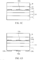
- FIGS. 1A to 1H show a method of manufacturing a semiconductor light-emitting device in accordance with an embodiment of the application.
- FIG. 1A shows a semiconductor epitaxial stack 110 including an n-type semiconductor layer 112, an active layer 114, and a p-type semiconductor layer 116 on a growth substrate 10.
- the n-type semiconductor layer 112, the active layer 114, and the p-type semiconductor layer 116 can be sequentially formed on the growth substrate 10 by conventional epitaxial growth process.
- the material of the growth substrate 10 comprises GaAs, germanium (Ge), indium phosphide (InP), sapphire (Al 2 O 3 ), silicon carbide (SiC), silicon (Si), lithium aluminum oxide (LiAlO 2 ), zinc oxide (ZnO), gallium nitride (GaN), or aluminum nitride (AlN).
- the n-type semiconductor layer 112 can be aluminum gallium indium phosphide (AlGaInP) series material or other materials; the material of the p-type semiconductor layer 116 can be GaP or other materials; the material of the active layer 114 comprises aluminum gallium indium phosphide (AlGaInP) series material, aluminum gallium indium nitride (AlGaInN) series material or zinc oxide (ZnO) series material, and the structure of the active layer 114 comprises single heterostructure (SH), double heterostructure (DH), double-side double heterostructure (DDH), or multi-quantum well (MWQ) structure. Specifically, the active layer 114 can be made of intrinsic, p-type or, n-type semiconductor material.
- the active layer 114 While an electrical current flows through the semiconductor epitaxial stack 110, the active layer 114 is able to emit a light.
- the active layer 114 is made of aluminum gallium indium phosphide (AlGaInP) series material, the active layer 114 is able to emit an amber series of light, such as a red light, an orange light and a yellow light.
- AlGaInN aluminum gallium indium nitride
- the active layer 114 is able to emit a blue or a green light.
- the semiconductor epitaxial stack 110 can include more semiconductor layers with different functions.
- FIG. 1B shows that the p-side electrodes 120a, 120b are patterned on the p-type semiconductor layer 116 by lithography process with sputtering, thermal deposition, or electroplating method.
- the material of the p-side electrodes 120a, 120b can be metal, such as Au, Ag, Cu, Al, Pt, Ni, Ti, Sn, and the alloy thereof or the stacking layers thereof.
- a first support substrate 20 is prepared, and a first adhesive layer 135 is formed on the first support substrate 20 by spin coating or deposition. And, the semiconductor epitaxial stack 110 is adhered to the first support substrate 20 with the first adhesive layer 135. Then, the growth substrate 10 can be removed by wet etching or laser lift-off.
- the first support substrate 20 can be made from single material and can be composite substrate which is made from combination of different materials.
- the first support substrate 20 can include a first substrate and a second substrate which is bonded with the first substrate (not shown).
- the material of the support substrate 20 comprises inorganic material, such as sapphire (Al 2 O 3 ), lithium aluminum oxide (LiAlO 2 ), zinc oxide (ZnO), gallium nitride (GaP), glass and aluminum nitride (AlN), or organic polymer material.
- a transferring structure is formed by the semiconductor epitaxial stack 110 transferred to the first support substrate 20 and the first support substrate 20.
- a portion of the surface of the p-type semiconductor layer 116 can be roughened by wet etching or dry etching.
- the patterned n-side electrodes 130a, 130b are formed on the exposed surface of the n-type semiconductor layer 112 by lithography process with sputtering, thermal deposition, or electroplating as shown in FIG. 1D .
- the material of the n-side electrodes 130a, 130b can be metal, such as Au, Ag, Cu, Al, Pt, Ni, Ti, Sn, and the alloy thereof or the stacking layers thereof.
- FIG. 1E shows that, in order to fit different processes of fabricating different semiconductor light-emitting devices, the following processes on the n-side electrodes 130a, 130b can be the same or different.
- a metal oxide transparent conductive layer 140 is formed on the surface of the semiconductor epitaxial stack 110 by CVD or PVD. Then, a reflective layer 150 is formed on a portion of the metal oxide transparent conductive layer 140.
- the material of the metal oxide transparent conductive layer 140 comprises ITO, IZO, InO, SnO, FTO, ATO, CTO, AZO, GZO or the combination thereof;
- the material of the reflective layer 150 comprises metal, such as Au, Ag, Cu, Cr, Al, Pt, Ni, Ti, Sn, Be or the alloy or the stacking layers thereof or Distributed Bragg Reflector (DBR), wherein DBR is made from the stacking layers comprising Al 2 O 3 , SiO 2 , TiO 2 or AlN.
- DBR Distributed Bragg Reflector
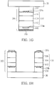
- FIG. 1F shows a side view of multiple first epitaxial units 201 and multiple second epitaxial units 202 above the first substrate 20 disclosed in the embodiment, which are totally divided by using dry etching in order to break off the electrical connection through the semiconductor epitaxial stack 110.
- the semiconductor epitaxial stack 110 is divided into the first epitaxial units 201 and the second epitaxial units 202 by forming a patterned photoresist layer (not shown) on the surface of the n-type semiconductor layer 112 and then using the dry etching, such as Inductively Coupled Plasma (ICP) and Plasma Etching (PE), to etch from the n-type semiconductor layer 112.
- the first epitaxial units 201 and the second epitaxial units 202 have different geometric shapes and areas, wherein each of the first epitaxial units 201 has the p-side electrode 120a and the n-side electrode 130a as shown in FIG. 1G , and each of the second epitaxial units 202 has the p-side electrode 120b and the n-side electrode 130b as shown in FIG.1H .
- the second epitaxial unit 202 is about around the first epitaxial unit 201 from the top view.
- FIG. 1F shows, in order to increase the light-emitting efficiency of the semiconductor light-emitting device, a portion of the surface of the n-type semiconductor layer 112 of the first epitaxial unit 201 or/and the second epitaxial unit 202 can be roughened by wet etching or dry etching.
- a patterned second adhesive layer 230 is formed on a portion of the surface of the semiconductor epitaxial stack 110, which is corresponding to the position of the second epitaxial units 202, by spin coating or deposition through a patterned mask, such as patterned photoresist.
- the portion of the semiconductor epitaxial stack 110 corresponding to the second epitaxial units 202 is prepared for being transferred again.
- the next step is to prepare a second support substrate 30.
- the second support substrate 30 is adhered to the second epitaxial units 202 with the patterned second adhesive layer 230 by heating or pressing.
- a laser is irradiated through the first support substrate 20 to dissolve the first adhesive layer 135 between the first support substrate 20 and the p-type semiconductor layer 116, and then the second epitaxial units 202 are transferred to the second support substrate 30.
- the remaining first adhesive layer 135 on the surface of the second epitaxial units 202 on the second support substrate 30 is removed by dry or wet etching.
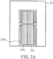
- FIGS. 3A and 4A show the first support substrate 20 with the first epitaxial units 201 and the second support substrate 30 with the second epitaxial units 202, wherein the top views thereof are respectively shown in FIGS. 3A and 4A .
- FIG. 4A show a top view of the second epitaxial units 202, wherein the second epitaxial units 202 are arranged in a U-shape.
- the first support substrate 20 and one of the first epitaxial units 201 are formed as a semiconductor light-emitting device 200
- the second support substrate 30 and the second epitaxial units 202 are formed as a semiconductor light-emitting device 300, wherein the top views thereof are respectively shown in FIGS. 3C and 4C .
- the second epitaxial units 202 and the first support substrate 20 are separated by the laser to dissolve the first adhesive layer 135.
- a material which has low adhesion with the first support substrate 20, such as SiO 2 can be used as the first adhesive layer 135.
- the second epitaxial units 202 can be separated from the first support substrate 20 by physical mechanical force after the second epitaxial units 202 are selectively adhered to the second substrate 30 through the patterned second adhesive layer 230.
- FIGS. 2A to 2H show a method of manufacturing a semiconductor light-emitting device in accordance with another embodiment of present application.
- FIG. 2A shows a semiconductor epitaxial stack 2110 including an n-type semiconductor layer 2112, an active layer 2114, and a p-type semiconductor layer 2116 on a growth substrate 210.
- the n-type semiconductor layer 2112, the active layer 2114, and the p-type semiconductor layer 2116 can be sequentially formed on the growth substrate 210 by conventional epitaxial growth process.
- the material of the growth substrate 210 comprises GaAs, germanium (Ge), indium phosphide (InP), sapphire, (Al 2 O 3 ), silicon carbide (SiC), silicon (Si), lithium aluminum oxide (LiAlO 2 ), zinc oxide (ZnO), gallium nitride (GaN) or aluminum nitride (AlN).
- the n-type semiconductor layer 2112 can be aluminum gallium indium phosphide (AlGaInP) series material or other materials; the material of the p-type semiconductor layer 2116 can be GaP or other materials; the material of the active layer 2114 comprises aluminum gallium indium phosphide (AlGaInP) series material, aluminum gallium indium nitride (AlGaInN) series material or zinc oxide (ZnO) series material, and the structure of the active layer 2114 comprises single heterostructure (SH), double heterostructure (DH), double-side double heterostructure (DDH), or multi-quantum well (MWQ) structure. Specifically, the active layer 2114 can be made of intrinsic, p-type, or n-type semiconductor material.
- the active layer 2114 While an electrical current flows through the semiconductor epitaxial stack 2110, the active layer 2114 is able to emit a light.
- the active layer 2114 is made of aluminum gallium indium phosphide (AlGaInP) series material, the active layer 2114 is able to emit an amber series of light, such as a red light, an orange light, and a yellow light.
- AlGaInN aluminum gallium indium nitride
- the active layer 2114 is able to emit a blue or a green light.
- the semiconductor epitaxial stack 2110 can include more semiconductor layers with different functions.
- FIG. 2B shows that the p-side electrodes 2120a, 2120b are patterned on the p-type semiconductor layer 2116 by lithography process with sputtering, thermal deposition, or electroplating.
- the material of the p-side electrodes 2120a, 2120b can be metal, such as Au, Ag, Cu, Al, Pt, Ni, Ti, Sn, and the alloy thereof or the stacking layers thereof.
- FIG. 2C shows, after the p-side electrodes 2120a, 2120b are formed, a support substrate 220 is provided, and a patterned sacrificial layer 2123 is formed on a surface of the support substrate 220 by lithography process.
- the position of the patterned sacrificial layer 2123 is corresponding to multiple second epitaxial units which are prepared to be transferred in the later step.
- a first adhesive layer 2135 is formed by spin coating or deposition.
- the semiconductor epitaxial stack 2110 is adhered to the first support substrate 220 by the first adhesive layer 2135.
- the first adhesive layer 2135 can be coated on the surface of the first support substrate 220 for covering the patterned sacrificial layer 2123.
- the first adhesive layer 2135 can also be coated on the surface of the p-type semiconductor layer 2116 and cover the p-side electrodes 2120a, 2120b. Then, the semiconductor epitaxial stack 2110 and the first support substrate 220 are bonded by heating and/or pressing. Finally, the growth substrate 210 is removed by wet etching or laser lift-off to form the structure shown in FIG. 2C .
- the first support substrate 220 is not limited to a single material and can be composite substrate which is made from combination of different materials.
- the first support substrate 220 can include a first substrate and a second substrate which is bonded with the first substrate (not shown).
- the material of the support substrate 220 comprises inorganic material, such as sapphire (Al 2 O 3 ), lithium aluminum oxide (LiAlO 2 ), zinc oxide (ZnO), gallium nitride (GaP), glass and aluminum nitride (AlN), or organic polymer material.
- sapphire Al 2 O 3
- LiAlO 2 lithium aluminum oxide
- ZnO zinc oxide
- GaP gallium nitride
- AlN aluminum nitride
- FIG. 2C shows, in order to increase the light-emitting efficiency of the semiconductor light-emitting device made from the semiconductor epitaxial stack 2110, a portion of the surface of the p-type semiconductor layer 2116 can be roughened by wet etching or dry etching.
- the patterned n-side electrodes 2130a, 2130b are formed on the exposed surface of the n-type semiconductor layer 2112 by lithography process with sputtering, thermal deposition, or electroplating as shown in FIG. 2D .
- the material of the n-side electrodes 2130a, 2130b can be metal, such as Au, Ag, Cu, Al, Pt, Ni, Ti, Sn, and the alloy thereof or the stacking layers thereof.
- FIG. 2E shows that, in order to fit different processes of fabricating different semiconductor light-emitting devices, the following processes on the n-side electrodes 2130a, 2130b can be the same or different.
- a metal oxide transparent conductive layer 2140 and/or a reflective layer 2150 can be formed on the surface of the n-type semiconductor layer 2112 by CVD or PVD.
- the material of the metal oxide transparent conductive layer 2140 comprises ITO, IZO, InO, SnO, FTO, ATO, CTO, AZO, GZO, or the combination thereof;
- the material of the reflective layer 2150 comprises metal, such as Au, Ag, Cu, Cr, Al, Pt, Ni, Ti, Sn, Be, or the alloy or the stacking layers thereof.
- FIG. 2F shows a side view of multiple first epitaxial units 2201 and multiple second epitaxial units 2202 above the first substrate 220 disclosed in the embodiment, which are divided by dry etching. And, the first adhesive layer 2135 and the patterned sacrificial layer 2123 are also divided.
- the semiconductor epitaxial stack 2110 is divided into the first epitaxial units 2201 and the second epitaxial units 2202 by forming a patterned photoresist layer (not shown) on the surface of the n-type semiconductor layer 2112 and then the dry etching, such as Inductively Coupled Plasma (ICP) and Plasma Etching (PE), to etch from the n-type semiconductor layer 2112.
- ICP Inductively Coupled Plasma
- PE Plasma Etching
- the first epitaxial units 2201 and the second epitaxial units 2202 have different geometric shapes and areas, wherein each of the first epitaxial units 2201 has the p-side electrode 2120a and the n-side electrode 2130a, and each of the second epitaxial units 2202 has the p-side electrode 2120b and the n-side electrode 2130b.
- a portion of the surface of the n-type semiconductor layer 2112 of the first epitaxial unit 2201 or/and the second epitaxial unit 2202 can be roughened by wet etching or dry etching. Then, a patterned second adhesive layer 2230 is formed on a portion of the surface of the semiconductor epitaxial stack 2110 prepared for being transferred again, which is corresponding to the portion of the surface of the n-type semiconductor layer 2112 of the second epitaxial units 2202, by spin coating or deposition through a patterned mask, such as patterned photoresist.
- the material of the patterned second adhesive layer 2230 comprises organic material, such as Acrylic acid, Unsaturated polyester, Epoxy, Oxetane, Vinyl ether, Nylon, PP, PBT, PPO, PC, ABS, and PVC; metal, such as Ti, Au, Be, W, Al, Ge, Cu, and the alloy thereof; oxide, such as ITO, CTO, ATO, IZO, AZO, ZTO, ZnO, and SiO x ; or nitride, such as SiN x .
- organic material such as Acrylic acid, Unsaturated polyester, Epoxy, Oxetane, Vinyl ether, Nylon, PP, PBT, PPO, PC, ABS, and PVC
- metal such as Ti, Au, Be, W, Al, Ge, Cu, and the alloy thereof
- oxide such as ITO, CTO, ATO, IZO, AZO, ZTO, ZnO, and SiO x
- nitride such as SiN x .
- the next step is to prepare a second support substrate 230.
- the second epitaxial units 2202 are adhered on the second support substrate 230 with the patterned second adhesive layer 2230 by heating or pressing.
- the adhesion of the patterned sacrificing layer 2123 is decreased by wet etching, dry etching, mechanical force separating, illuminating UV, or heating, the second epitaxial units 2202 are transferred to the second support substrate 230.
- FIGS. 2G and 2H show the first support substrate 220 with the first epitaxial units 2201 and the second support substrate 230 with the second epitaxial units 2202, wherein the top views thereof are respectively shown in FIGS. 3A and 4A .
- the first support substrate 220 and one of the first epitaxial units 2201 are formed as a semiconductor light-emitting device 200
- the second support substrate 230 and the second epitaxial units 2202 are formed as a semiconductor light-emitting device 300, wherein the top views thereof are respectively shown in FIGS. 3C and 4C .
- the material of the patterned sacrificial layer 2123 comprises metal, such as Ti, Au, Ag, W, Al, Cr, Cu, Pt, and the combination thereof; UV dissociating glue; or dielectric material, such as SiO x and SiN x .
- the patterned sacrificial layer 2123 can be removed by wet etching, dry etching or illuminating UV, or the adhesion between the patterned sacrificial layer 2123 and the first support substrate 220 can be decreased by heating, and then the second epitaxial unit 2202 and the first support substrate 220 is separated by mechanical force separating.
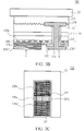
- the side view and the top view of the semiconductor light-emitting device 200 which can be a flip-chip light-emitting device, are respectively shown in FIGS. 3B and 3C .
- a conductive through hole 134 is formed by etching the semiconductor epitaxial stack 110(2110) along a direction perpendicular to the surface of the first support substrate 20 from the n-type semiconductor layer 112(2112) to the p-side electrode 120a(2120a).
- An insulative layer 132 is formed on the side wall of the conductive through hole 134 by CVD or PVD to electrically insulate from the semiconductor epitaxial stack 110(2110), and then a metal conductive structure is formed in the conductive through hole 134 to form a p-type extension 130a' which extends to the surface of the n-type semiconductor layer 112(2112).
- the p-type extension 130a' and the n-type extension 130a" on the n-side electrodes 130a(2130a) are formed at the same step and are able to constitute the two extensional electrodes of the flip-chip type semiconductor light-emitting device 200.
- the surface a of the n-type extension 130a" and the surface b of the p-type extension 130a' on the same side of the first epitaxial unit 201 can be designed to be in the same high level for forming a more reliable and more stable connecting structure.
- FIGS. 4B and 4C respectively show the side view and the top view of the semiconductor light-emitting device 300, which is a high-voltage single chip LED device, being transferred to the second support substrate 30.
- the process steps and the structure are shown in FIGS. 4A , 5A , 5B , 4B and 4C .
- the second epitaxial unit 202(2202) is transferred to the second substrate 30(230), wherein the p-side electrodes 120b(2120b) are directly formed on the p-type semiconductor layer 116(2116) after the semiconductor epitaxial stack 110 is formed on the growth substrate 10(210), and the n-side electrodes 130b(2130b) are directly formed on the n-type semiconductor layer 112(2112) after the first substrate transferring process. Therefore, the n-side electrodes 130b(2130b) are buried under the n-type semiconductor layer 112(2112) (indicated by dotted line) after the second epitaxial unit 202(2202) is transferred to the second support substrate 30(230).
- the second epitaxial unit 202(2202) has the p-side electrodes 120b(2120b) on the surface thereof, and the patterned second adhesive layer 230(2230) covers the second epitaxial unit 202(2202) and the surface of the p-side electrodes 120b(2120b).
- the second epitaxial unit 202(2202) is divided into multiple third epitaxial units 202' by dry etching, such as Reactive Ion Etching (RIE), Inductively Coupled Plasma (ICP), and Plasma Etching (PE).
- RIE Reactive Ion Etching
- ICP Inductively Coupled Plasma
- PE Plasma Etching
- an insulative layer 232 is patterned and formed on a portion of the surface of each of the third epitaxial units 202' and the side wall between the neighboring third epitaxial units 202' by PVD or CVD and patterning process.
- FIG. 5B shows a side view of the two neighboring third epitaxial units 202' during the process.
- the material of the insulative layer 232 is SiO 2 .
- the material of the insulative layer 232 comprises SiN x , Al 2 O 3 , AlN or the combination thereof.
- a metal conductive connection structure 125 is formed between the neighboring third epitaxial units 202' by lithography process to electrically connect the n-side electrode 130b' of one of the third epitaxial units 202' and the p-side electrode 120b of the other one in an electrical series connection to form a high-voltage single chip semiconductor light-emitting device 300 shown in FIGS. 4B and 4C .
- the p-side electrode 120b(2120b) and the n-side electrode 130b' are respectively on the opposite sides of the third epitaxial units 202'.
- the p-side electrode 120b(2120b) and the n-side electrode 130b' of the two of the third epitaxial units 202' at the ends of the semiconductor light-emitting device 300 are respectively connected to a p-type electrode pad 102b' and an n-type electrode pad 120b", wherein the p-side electrodes 120b(2120b), the n-side electrodes 130b', the p-type electrode pad 102b' and the n-type electrode pad 120b" can be formed with the metal conductive connection structure 125 in the same step. As shown in FIG.
- the p-type electrode pad 102b' and the n-type electrode pad 120b" are formed on the surface of the second support substrate 30(230) beyond the third epitaxial units 202' and do not overlap with the surface of the third epitaxial units 202' for increasing the light extracting efficiency of the semiconductor light-emitting device 300.
- the third epitaxial units 202' can also be connected to an electrical parallel structure between the neighboring third epitaxial units 202'.
- the method of electrically connecting the third epitaxial units 202' further comprises forming a patterned electrically conductive structure on the surface of the second support substrate 30(230), and then bonding each of the third epitaxial units 202' in flip-chip type on the second support substrate 30(230) and electrically connecting to the patterned electrically conductive structure.
- the third epitaxial units 202' can also be connected in series or parallel to form the semiconductor light-emitting device.
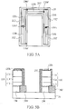
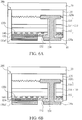
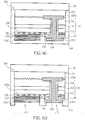
- the semiconductor light-emitting device 200 can be produced as an encapsulated semiconductor light-emitting device 400 by subsequent processes, and the side view and the top view are respectively shown in FIGS. 6C and 6D .
- FIGS. 6A to 6C show the process and the structure of manufacturing the semiconductor light-emitting device 400 for clearly presenting the encapsulated semiconductor light-emitting device 400.
- FIG. 6A shows a transparent structure 40 covering and surrounding the semiconductor light-emitting device 200 and the side wall of each of the epitaxial units thereof by spin coating and deposition, wherein the transparent structure 40 is transparent to the light emitted from the semiconductor light-emitting device 200, and the transparent structure 40 is used to encapsulate the semiconductor light-emitting device 200 for increasing the mechanical strength the semiconductor light-emitting device 200, disclosed in the embodiment.
- the material of the transparent structure 40 comprises Epoxy, Polyimide, Benzocyclobutene, Perfluorocyclobutane, SU8 photoresist, Acrylic Resin, Palymethylmethacrylate, Poly ethylene terephthalate, Polycarbonate, Polyetherimide, Fluorocarbon Polymer, Glass, Al 2 O 3 , SINR, SOG, Teflon, or the combination thereof.
- FIG. 6B shows that a portion of the transparent structure 40 is removed to expose the p-type extension 130a' and the n-type extension 130a".
- an insulative scattering layer 410 is formed to cover the surface of the transparent structure 40 and a portion of the surface and side surface of the p-type extensions 130a' and the n-type extension 130a" by spin coating, deposition, stencil printing, or screen printing.
- the insulative scattering layer 410 can be used to scatter and reflect light and insulate against electrical current so the use of scattering material, reflective material, and insulative material can be reduced.
- the material of the insulative scattering layer 410 comprises Epoxy, SiO x , Al 2 O 3 , TiO 2 , Silicone, Resin, or the combination thereof.
- a portion of the insulative scattering layer 410 which is corresponding to the position of the p-type extensions 130a' and the n-type extension 130a", is removed by lithography process to form openings 411, 412 corresponding to the position of the p-type extensions 130a' and the n-type extension 130a".
- the insulative scattering layer 410 covers the side wall and a portion surface of the p-type extensions 130a' and the n-type extension 130a" in order to increase the light extracting efficiency.
- a p-type bonding pad 1310 and an n-type bonding pad 1320 are respectively formed in the openings 411, 412 above the transparent structure 40 and the insulative scattering layer 410 for wire bonding by chemical plating, electroplating, or sputtering with mask.
- the encapsulated semiconductor light-emitting device 400 is completed as shown in FIG. 6E . Because the semiconductor epitaxial stack 110 is surrounded by encapsulating structure, the semiconductor light-emitting device 400 has better heat resistance, moisture resistance and oxidative stability. The semiconductor light-emitting device 400 is able to electrically connect to the printed circuit board by wire bonding or flip-chip bonding to form a light-emitting device, such as light bulb, back light unit, and vehicle lamp.
- FIG. 8 shows a top view of the semiconductor light-emitting device 400.
- the view along the direction D (shown in FIG. 6E ) perpendicular to the first support substrate 20 shows that the first epitaxial unit 201 of the semiconductor light-emitting device 200 is surrounded by the transparent structure 40, wherein and the transparent structure 40 is covered by an insulative scattering layer (not shown).
- a portion of the insulative scattering layer is removed to form the openings 411, 412 on the first epitaxial unit 201, wherein the openings 411, 412 are overlapped by the p-type bonding pad 1310 and the n-type bonding pad 1320 which electrically connect the first epitaxial unit 201.
- the p-type bonding pad 1310 and the n-type bonding pad 1320 are out of the range of the first epitaxial unit 201. Namely, the view along the direction perpendicular to the first support substrate 20 shows that a portion of the p-type bonding pad 1310 and a portion of the n-type bonding pad 1320 do not overlap with the first epitaxial unit 201.
- the aforementioned structure is able to increase the area of the metal bonding pad.
- the semiconductor light-emitting device 400 electrically connects the external substrate, such as printed circuit board, the connection between the devices is more reliable and more stable.
- the exposed surface of the p-type bonding pad 1310 and the exposed surface of the n-type bonding pad 1320 on the same side of the first epitaxial unit 201 are in the same high level.
- the p-type bonding pad 1310 and the n-type bonding pad 1320 are used for inducing an external electrical current, and the material thereof comprises Cu, Sn, Au, Ni, Ti, Pb, Cu-Sn, Cu-Zn, Cu-Cd, Sn-Pb-Sb, Sn-Pb-Zn, Ni-Sn, Ni-Co, Au alloy, Au-Cu-Ni-Au, or the combination thereof.
- the view along the direction perpendicular to the substrate shows that the epitaxial unit can be formed to different shapes for meeting different demands.
- FIG. 9 shows that the epitaxial unit can be cut into square or cross disclosed in the embodiment.
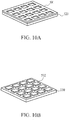
- the semiconductor epitaxial stack 5110 on the growth substrate 510 is divided into a first epitaxial unit 501 and a second epitaxial unit 502, and then the first epitaxial unit 501 and the second epitaxial unit 502 are respectively transferred to the first support substrate 520 and the second support substrate 530 as shown in FIGS. 10A and 10B .
- an electrically conductive layer can fully contact the surface of the support substrate, or be patterned to partially contact the support substrate for electrically connecting the epitaxial units on the support substrate, wherein the electrically conductive layer is made of transparent metal oxide conductive layer which is pervious to the light emitted from the epitaxial units.
- the transparent metal oxide conductive layer can be made by CVD or PVD, and the material of the transparent metal oxide conductive layer comprises ITO, IZO, InO, SnO, FTO, ATO, CTO, AZO, GZO or the combination thereof.
- the transparent metal oxide conductive layer can also be used for the material of the adhesive layer and formed with the substrate transferring process as mentioned above.
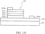
- FIGS. 11A to 11E show a method of manufacturing a semiconductor light-emitting device by using a transparent metal oxide conductive layer as an adhesive material in accordance with another embodiment.
- a semiconductor epitaxial stack is transferred from the growth substrate 510 to a first support substrate 520 with a first adhesive layer 5130 on thereof by the above mentioned method or a conventional method. And then, the semiconductor epitaxial stack is patterned and divided into a first epitaxial unit 501 and a second epitaxial unit 502.
- the first adhesive layer 5130 comprises organic material, such as Acrylic acid, Unsaturated polyester, Epoxy, Oxetane, Vinyl ether, Nylon, PP, PBT, PPO, PC, ABS, and PVC; metal, such as Ti, Au, Be, W, Al, Ge, Cu, and the alloy thereof; oxide, such as ITO, CTO, ATO, IZO, AZO, ZTO, ZnO, and SiO x ; or nitride, such as SiN x .
- organic material such as Acrylic acid, Unsaturated polyester, Epoxy, Oxetane, Vinyl ether, Nylon, PP, PBT, PPO, PC, ABS, and PVC
- metal such as Ti, Au, Be, W, Al, Ge, Cu, and the alloy thereof
- oxide such as ITO, CTO, ATO, IZO, AZO, ZTO, ZnO, and SiO x
- nitride such as SiN x .
- a semiconductor epitaxial stack includes an n-type semiconductor layer 5112, an active layer 5114 and a p-type semiconductor layer 5116.
- the semiconductor epitaxial stack is patterned and divided into a first epitaxial unit 501 and multiple second epitaxial units 502.
- two second adhesive layers 5230 are respectively formed on the surface of each second epitaxial unit 502 and on the surface of a second support substrate 530, wherein the two second adhesive layers 5230 are made of the transparent metal oxide conductive layer.
- the two second adhesive layers 5230 are connected by heating or pressing.
- the second adhesive layers 5230 can be formed on the full surface of the second support substrate 530 or patterned on the partial surface of the second support substrate 530.
- the first adhesive layer 5130 between the first support substrate 520 and the second epitaxial units 502 can be melted by illuminating laser or UV, and then the second epitaxial units 502 are transferred to the second support substrate 530. After the second epitaxial units 502 are adhered to the second support substrate 530, the remaining first adhesive layer 5130 on the surface of the each second epitaxial unit 502 on the second support substrate 530 can be removed by dry or wet etching. Finally, the first epitaxial unit 501 and the multiple second epitaxial units 502 are respectively on the first support substrate 520 and the second support substrate 530 as shown in FIGS. 10A and 10B .
- the method to separate the first support substrate 520 and the second epitaxial units 502 includes melting the first adhesive layer 5130 by illuminating laser as mentioned above.
- a material with low adhesion force with the first support substrate 520 such as SiO 2 , is used as the first adhesive layer 5130 so a mechanical force can be applied to separate the first support substrate 520 and the second epitaxial units 502 after the second epitaxial units 502 are adhered to the second support substrate 530 by forming a patterned second adhesive layer 5230 on the surfaces of the second epitaxial units 502 which are chosen to be transferred again.
- the second support substrate 530 After the second epitaxial units 502 and the first support substrate 520 are separated, the second support substrate 530 has the second epitaxial units 502 thereon which are transferred again. Next, the second support substrate 530 can be patterned and divided into multiple second support substrate units (not shown) for forming light-emitting devices, wherein each of the second support substrate units has one or multiple second epitaxial units 502 thereon.
- FIG. 11E shows that a single second support substrate unit 530' supports one second epitaxial unit 502 thereon.
- the patterned second adhesive layer 5230 is made of transparent metal oxide conductive layer, the patterned second adhesive layer 5230 is able to electrically connect the n-type semiconductor layer 5112 and extend to the surface of the second support substrate unit 530' beyond the second epitaxial unit 502.
- an n-side electrode 5120a and a p-side electrode 5120b are respectively patterned on the surface of the second support substrate unit 530' beyond the second epitaxial unit 502 and on the surface of the p-type semiconductor layer 5116 by lithography process with sputtering, thermal deposition, or electroplating.
- the n-side electrode 5120a produced by the aforementioned process is not on the surface of the second epitaxial unit 502 for avoiding shading the light and increasing the light extracting efficiency.
- the first epitaxial unit 501 which remains on the first support substrate 520, can be divided from the first support substrate 520 to form different semiconductor devices by subsequent different processes.
- FIG. 13 shows that the remaining first epitaxial unit 501 can further form multiple semiconductor light-emitting devices with cross-shaped epitaxial units 501' represented by the dotted line 510 by the cutting method disclosed in the embodiments.
- FIGS. 14A to 14D indicate, the process disclosed in the embodiment can efficiently utilize the entire semiconductor epitaxial stack on the substrate.
- FIG. 14A shows a top view of the semiconductor light-emitting device 500 comprising the cross epitaxial unit 501'
- FIG. 14B shows an oblique side view thereof.
- FIG. 14A shows a top view of the semiconductor light-emitting device 500 comprising the cross epitaxial unit 501'
- FIG. 14B shows an oblique side view thereof.
- a transparent metal oxide conductive layer 5280 is formed on the whole top surface of the second support substrate unit 530', and the patterned n-side electrode 5120a and the p-side electrode 5120b are respectively formed on the surface of the transparent metal oxide conductive layer 5280 extending out from the second epitaxial unit 502 and on the surface of the p-type semiconductor layer 5116, wherein the patterned n-side electrode 5120a and the p-side electrode 5120b respectively and electrically contact the n-type semiconductor layer 5112 and the p-type semiconductor layer 5116.
- FIGS. 14C and 14D respectively show a top view and an oblique side view of the semiconductor light-emitting device 600 comprising the cross epitaxial unit 501' in accordance with another embodiment.
- the partially patterned transparent metal oxide conductive layer 5280 which is used as an adhesion layer, is disposed on the surface of the second support substrate unit 530', wherein the second support substrate unit 530' is an insulative substrate, such as sapphire (Al 2 O 3 ).
- the p-side electrode 5120b is disposed on the region of the surface of the second support substrate unit 530' not covered by the transparent metal oxide conductive layer 5280, and a p-type extension 5120b', which extends from the p-side electrode 5120b, electrically contacts the p-type semiconductor layer 5116.
- the patterned n-side electrode 5120a is disposed on the surface of the patterned second adhesive layer 5230 beyond the second epitaxial unit 502 and electrically contacts the n-type semiconductor layer 5112 through the patterned second adhesive layer 5230.
- the cross epitaxial unit 501' is made from the first epitaxial unit 501, which has symmetrical shape and has two different symmetrical surfaces A' and B' perpendicular to the substrate, and the end portions of the cross epitaxial unit 501' are near the edges of the second support substrate unit 530'. Therefore, the portion of the second support substrate unit 530' uncovered by the cross epitaxial unit 501' can be partitioned into four regions.
- the first epitaxial unit 501 can be made to L-shape epitaxial units or irregular polygon epitaxial units, and the second support substrate unit 530' can also be partitioned into multiple regions, not limited to 4 regions.
- the second support substrate 530 is an insulative substrate, such as sapphire (Al 2 O 3 ) substrate, aluminum nitride (AlN) substrate, glass substrate, and organic polymer substrate. And, the second support substrate 530 can also be an electrically conductive substrate, such as lithium aluminum oxide (LiAlO 2 ) substrate, zinc oxide (ZnO) substrate and gallium nitride (GaP) substrate. And, the second support substrate 530 can be a transparent substrate or a reflective substrate.
- the material of the second support substrate 530 can also be made of a high thermal dissipation material with a thermal conductivity coefficient larger than 24W/m*k, such as Cu, Wu, AlN, Metal Matrix Composite (MMC), Ceramic Matrix Composite (CMC), SiC, Al, Si, Diamond, or the combination thereof.
- MMC Metal Matrix Composite
- CMC Ceramic Matrix Composite
- the area of each of the transparent support substrates (20, 30) is larger than the area of the surface of the active layer 114 of the semiconductor epitaxial stack 110. While the light enters the transparent support substrates (20, 30) of which the refractivity is lower than the refractivity of the semiconductor epitaxial stack 110, since the transparent support substrates (20, 30) have larger area, more light can depart from the transparent support substrates (20, 30). As shown in FIGS. 12A and 12B , for the conventional flip-chip type light-emitting devices, the conventional flip-chip type light-emitting device and the active layer 114 thereof have the same areas.
- the area of the first support substrate 20 of the flip-chip type semiconductor light-emitting device 200 (shown in FIG. 3C ) is larger than twice the area of the surface of the active layer 114 thereof, which is different from the conventional flip-chip type light-emitting devices.
- the light-emitting devices 5000, 2000 are respectively formed by respectively connecting the light-emitting diodes to the corresponding circuits of the submounts 50', 20' through the tin solders 560, 260. In the meantime, there is more light L emitted from the active layer 114 which can be extracted from large support substrate 20 and not be absorbed again by the active layer 114.
- the light-emitting device 2000 has better light extracting efficiency than the light-emitting device 5000. Namely, as the large support substrate 20 is applied to the high-voltage semiconductor light-emitting device 300, the encapsulated semiconductor light-emitting device 400, or the semiconductor light-emitting devices 500, 600 made from the single second epitaxial units 502, the light extracting efficiencies thereof can also be improved.
- the number of the semiconductor epitaxial stack(s) on a single support substrate is not limited to one.
- a semiconductor epitaxial stack is formed on a larger first support substrate 20
- multiple the same first epitaxial units 201 and second epitaxial units 202 as shown in FIG. 7 can be formed by lithography process and transferring process.
- the multiple second epitaxial units 202 formed on the first support substrate 20 are transferred to the larger second support substrate 30 (such as a wafer) at the same time, and the first epitaxial units 201 remain on the first support substrate 20.
- the multiple semiconductor light-emitting devices 200 comprising the first epitaxial units 201, of which the size is the same as the size of the substrate shown in FIG. 3C , can be formed by cutting the first support substrate 20; and similarly, the multiple semiconductor light-emitting devices 300 comprising the third epitaxial units 202', of which the size is the same as the size of the substrate shown in FIG. 4C , can be formed by cutting the second support substrate 30.
- One of the semiconductor light-emitting devices 200 matches one of the semiconductor light-emitting devices 300, and one unit of a single semiconductor epitaxial stack 110 on a single substrate can form one semiconductor light-emitting devices 200 and one semiconductor light-emitting devices 300. Therefore, the semiconductor light-emitting devices 200, 300 should have approximately the same sizes. In other words, the areas of the substrates thereof are approximately the same as shown in FIGS. 3C and 4C .
Landscapes
- Led Devices (AREA)
- Led Device Packages (AREA)
- Physics & Mathematics (AREA)
- Engineering & Computer Science (AREA)
- Condensed Matter Physics & Semiconductors (AREA)
- General Physics & Mathematics (AREA)
- Manufacturing & Machinery (AREA)
Claims (16)
- Verfahren zum Herstellen einer Licht emittierenden Halbleiter-Diodenvorrichtung, das folgende Schritte umfasst:- Bereitstellen eines ersten Substrats (220);- Bereitstellen eines epitaktischen Halbleiterstapels (2110);- Bilden einer gemusterten Opferschicht (2123) zwischen dem ersten Substrat (220) und dem epitaktischen Halbleiterstapel (2110);- Kleben des ersten Substrats (220) an den epitaktischen Halbleiterstapel (2110) durch eine erste Klebeschicht (2135), wobei die erste Klebeschicht (2135) die Opferschicht (2123) abdeckt;- Mustern des epitaktischen Halbleiterstapel (2110) in mehrere epitaktische Einheiten (2201, 2202), wobei die Vielzahl epitaktischer Einheiten umfasst:mehrere erste epitaktische Einheiten (2201), wobei jede der ersten epitaktischen Einheiten (2201) eine erste geometrische Form und eine erste Fläche hat, undmehrere zweite epitaktische Einheiten (2202), wobei jede der zweiten epitaktischen Einheiten (2202) eine zweite geometrische Form und eine zweite Fläche hat, und die mehreren zweiten epitaktischen Einheiten (2202) der Position der gemusterten Opferschicht (2123) entsprechen;- Bereitstellen eines zweiten Substrats (230) mit einer Oberfläche;- Verringern des Haftens der gemusterten Opferschicht (2123);- danach Übertragen der mehreren zweiten epitaktischen Einheiten (2202) zu der Oberfläche des zweiten Substrats (230), und- Aufteilen des ersten Substrats (220), um mehrere erste Licht emittierende Halbleiter-Diodenvorrichtungen zu bilden, wobei jede der ersten Licht emittierenden Halbleiter-Diodenvorrichtungen eine der ersten epitaktischen Einheiten (2201) hat;wobei die erste geometrische Form von der zweiten geometrischen Form oder die erste Fläche von der zweiten Fläche unterschiedlich ist.
- Verfahren zum Herstellen einer Licht emittierenden Halbleiter-Diodenvorrichtung nach Anspruch 1, wobei der Schritt des Übertragens der mehreren zweiten epitaktischen Einheiten (2202) zu der Oberfläche des zweiten Substrats (230) ferner Folgendes umfasst:- Trennen der mehreren zweiten epitaktischen Einheiten (2202) von dem ersten Substrat (220), und- Kleben der mehreren zweiten epitaktischen Einheiten (2202) an das zweite Substrat (230).
- Verfahren zum Herstellen einer Licht emittierenden Halbleiter-Diodenvorrichtung nach Anspruch 1 oder 2, wobei der Schritt des Übertragens der mehreren zweiten epitaktischen Einheiten (2202) zu der Oberfläche des zweiten Substrats (230) ferner Folgendes umfasst:- Entfernen eines Abschnitts der ersten Klebeschicht (2135) auf den mehreren zweiten epitaktischen Einheiten (2202), nachdem die mehreren zweiten epitaktischen Einheiten (2202) zu dem zweiten Substrat (230) übertragen wurden.
- Verfahren zum Herstellen einer Licht emittierenden Halbleiter-Diodenvorrichtung nach Anspruch 3, das ferner das Bilden einer zweiten Klebeschicht (2230) auf einem Abschnitt der Oberfläche des zweiten Substrats (230) umfasst, wobei der Abschnitt der Oberfläche des zweiten Substrats (230) den Positionen der mehreren zweiten epitaktischen Einheiten (2202) entspricht.
- Verfahren zum Herstellen einer Licht emittierenden Halbleiter-Diodenvorrichtung nach Anspruch 1, wobei die erste geometrische Form und/oder die zweite geometrische Form ein Quadrat, Rechteck oder Kreuz umfasst.
- Verfahren zum Herstellen einer Licht emittierenden Halbleiter-Diodenvorrichtung nach Anspruch 1, wobei die erste Licht emittierende Halbleiter-Diodenvorrichtung nur eine der ersten epitaktischen Einheiten (2201) und eine erste Substrateinheit zum Tragen der ersten epitaktischen Einheit (2201) umfasst.
- Verfahren zum Herstellen einer Licht emittierenden Halbleiter-Diodenvorrichtung nach Anspruch 1, das ferner das Schneiden des zweiten Substrats (230, 530) umfasst, um mehrere zweite Licht emittierende Vorrichtungen zu bilden, wobei jede der mehreren zweiten Licht emittierenden Vorrichtungen mindestens eine der epitaktischen Einheiten (202, 2202) umfasst.
- Verfahren zum Herstellen einer Licht emittierenden Halbleiter-Diodenvorrichtung nach Anspruch 7, das ferner das Aufteilen jeder der zweiten epitaktischen Einheiten (202) in mehrere dritte epitaktische Einheiten (202') und das Aufteilen des zweiten Substrats (230, 530) in mehrere zweite Substrateinheiten umfasst, wobei jede der mehreren zweiten Licht emittierenden Halbleiter-Vorrichtungen die mehreren dritten epitaktischen Einheiten (202') umfasst und die zweite Substrateinheit die mehreren dritten epitaktischen Einheiten (202') trägt.
- Verfahren zum Herstellen einer Licht emittierenden Halbleiter-Diodenvorrichtung nach Anspruch 7, wobei jede der zweiten Licht emittierenden Halbleiter-Vorrichtungen zwei der mehreren zweiten epitaktischen Einheiten (202, 2202) umfasst, und eine zweite Substrateinheit, die von dem zweiten Substrat (230) getrennt ist, um die mehreren zweiten epitaktischen Einheiten (202, 2202) zu tragen.
- Verfahren zum Herstellen einer Licht emittierenden Halbleiter-Diodenvorrichtung nach Anspruch 8, das ferner das Bilden einer leitfähigen Verbindungsstruktur (125) umfasst, um die mehreren dritten epitaktischen Einheiten (202') in Reihe oder parallel zu schalten.
- Verfahren zum Herstellen einer Licht emittierenden Halbleiter-Diodenvorrichtung nach Anspruch 8, wobei die mehreren zweiten epitaktischen Einheiten (202, 2202) in U-Form eingerichtet sind.
- Verfahren zum Herstellen einer Licht emittierenden Halbleiter-Diodenvorrichtung nach Anspruch 1, das ferner das Entfernen der gemusterten Opferschicht (2123) umfasst.
- Verfahren zum Herstellen einer Licht emittierenden Halbleiter-Diodenvorrichtung nach Anspruch 8, das ferner das Bilden eines ersten Klebepads und eines zweiten Klebepads auf dem zweiten Substrat umfasst, wobei das erste Klebepad und das zweite Klebepad elektrisch mit mindestens einer der dritten epitaktischen Einheiten (202') verbunden sind.
- Verfahren zum Herstellen einer Licht emittierenden Halbleiter-Diodenvorrichtung nach Anspruch 13, wobei das erste Klebepad und das zweite Klebepad auf dem zweiten Substrat über eine Fläche des zweiten Substrats (230) hinaus, wo die dritten epitaktischen Einheiten gebildet sind, gebildet werden.
- Verfahren zum Herstellen einer Licht emittierenden Halbleiter-Diodenvorrichtung nach Anspruch 1, das ferner das Bilden einer leitfähigen Metalloxidschicht auf der Oberfläche des zweiten Substrats (530) umfasst.
- Verfahren zum Herstellen einer Licht emittierenden Halbleiter-Diodenvorrichtung nach Anspruch 15, das ferner das Bilden einer ersten Elektrode auf einer Fläche des zweiten Substrats, die mit der leitfähigen Metalloxidschicht abgedeckt ist, umfasst, wobei die erste Elektrode elektrisch mit der zweiten epitaktischen Einheit verbunden ist.
Priority Applications (2)
| Application Number | Priority Date | Filing Date | Title |
|---|---|---|---|
| EP17185339.3A EP3267467B1 (de) | 2012-11-12 | 2013-07-03 | Lichtemittierendes halbleiterelement |
| EP22150103.4A EP4016583A1 (de) | 2012-11-12 | 2013-07-03 | Lichtemittierendes halbleiterbauelement und verfahren zur herstellung davon |
Applications Claiming Priority (2)
| Application Number | Priority Date | Filing Date | Title |
|---|---|---|---|
| CN201210451045.1A CN103811593B (zh) | 2012-11-12 | 2012-11-12 | 半导体光电元件的制作方法 |
| PCT/CN2013/078766 WO2014071745A1 (zh) | 2012-11-12 | 2013-07-03 | 半导体发光元件及其制作方法 |
Related Child Applications (3)
| Application Number | Title | Priority Date | Filing Date |
|---|---|---|---|
| EP17185339.3A Division EP3267467B1 (de) | 2012-11-12 | 2013-07-03 | Lichtemittierendes halbleiterelement |
| EP17185339.3A Division-Into EP3267467B1 (de) | 2012-11-12 | 2013-07-03 | Lichtemittierendes halbleiterelement |
| EP22150103.4A Division EP4016583A1 (de) | 2012-11-12 | 2013-07-03 | Lichtemittierendes halbleiterbauelement und verfahren zur herstellung davon |
Publications (3)
| Publication Number | Publication Date |
|---|---|
| EP2919258A1 EP2919258A1 (de) | 2015-09-16 |
| EP2919258A4 EP2919258A4 (de) | 2016-04-27 |
| EP2919258B1 true EP2919258B1 (de) | 2017-10-25 |
Family
ID=50684012
Family Applications (3)
| Application Number | Title | Priority Date | Filing Date |
|---|---|---|---|
| EP13853036.5A Active EP2919258B1 (de) | 2012-11-12 | 2013-07-03 | Lichtemittierendes halbleiterbauelement und verfahren zur herstellung davon |
| EP17185339.3A Active EP3267467B1 (de) | 2012-11-12 | 2013-07-03 | Lichtemittierendes halbleiterelement |
| EP22150103.4A Pending EP4016583A1 (de) | 2012-11-12 | 2013-07-03 | Lichtemittierendes halbleiterbauelement und verfahren zur herstellung davon |
Family Applications After (2)
| Application Number | Title | Priority Date | Filing Date |
|---|---|---|---|
| EP17185339.3A Active EP3267467B1 (de) | 2012-11-12 | 2013-07-03 | Lichtemittierendes halbleiterelement |
| EP22150103.4A Pending EP4016583A1 (de) | 2012-11-12 | 2013-07-03 | Lichtemittierendes halbleiterbauelement und verfahren zur herstellung davon |
Country Status (6)
| Country | Link |
|---|---|
| US (6) | US9735312B2 (de) |
| EP (3) | EP2919258B1 (de) |
| JP (5) | JP6068672B2 (de) |
| KR (3) | KR101732992B1 (de) |
| CN (4) | CN108447855B (de) |
| WO (1) | WO2014071745A1 (de) |
Families Citing this family (23)
| Publication number | Priority date | Publication date | Assignee | Title |
|---|---|---|---|---|
| DE102013103079A1 (de) * | 2013-03-26 | 2014-10-02 | Osram Opto Semiconductors Gmbh | Optoelektronischer Halbleiterchip und Verfahren zur Herstellung eines optoelektronischen Halbleiterchips |
| DE102014102029A1 (de) * | 2014-02-18 | 2015-08-20 | Osram Opto Semiconductors Gmbh | Verfahren zur Herstellung von Halbleiterbauelementen und Halbleiterbauelement |
| CN105336706A (zh) * | 2014-08-06 | 2016-02-17 | 晶能光电(江西)有限公司 | 一种高压led芯片的制备方法 |
| GB201418772D0 (en) | 2014-10-22 | 2014-12-03 | Infiniled Ltd | Display |
| GB201418810D0 (en) | 2014-10-22 | 2014-12-03 | Infiniled Ltd | Display |
| CN105826355B (zh) * | 2016-05-03 | 2017-03-08 | 京东方科技集团股份有限公司 | 一种显示面板的制作方法 |
| US10153401B2 (en) * | 2016-12-16 | 2018-12-11 | Intel Corporation | Passivated micro LED structures suitable for energy efficient displays |
| TWI607558B (zh) * | 2017-01-10 | 2017-12-01 | 錼創科技股份有限公司 | 微型發光二極體晶片 |
| US11056614B2 (en) * | 2017-01-10 | 2021-07-06 | PlayNitride Inc. | Micro light-emitting diode chip |
| US10353243B2 (en) * | 2017-08-01 | 2019-07-16 | Innolux Corporation | Display device |
| US11955574B2 (en) * | 2017-10-05 | 2024-04-09 | International Business Machines Corporation | Photovoltaic cell form ultra-small IOT device with multi-level voltage output |
| JP6431631B1 (ja) | 2018-02-28 | 2018-11-28 | 株式会社フィルネックス | 半導体素子の製造方法 |
| CN109148652B (zh) * | 2018-08-23 | 2020-08-25 | 上海天马微电子有限公司 | 无机发光二极管显示面板及其制作方法和显示装置 |
| US11664363B2 (en) * | 2018-10-17 | 2023-05-30 | Seoul Viosys Co., Ltd. | Light emitting device and method of manufacturing the same |
| US10796928B1 (en) * | 2019-06-27 | 2020-10-06 | Advanced Semiconductor Engineering, Inc. | Wiring structure and method for manufacturing the same |
| US12106980B2 (en) * | 2019-07-22 | 2024-10-01 | Osram Opto Semiconductors Gmbh | Adhesive transfer stamp and method for transferring a semiconductor chip using an adhesive transfer stamp |
| CN114080677B (zh) * | 2019-10-15 | 2026-01-16 | 三星电子株式会社 | 显示模块及其制造方法 |
| KR102906048B1 (ko) * | 2020-10-07 | 2026-01-02 | 삼성디스플레이 주식회사 | 표시 장치 및 그 제조 방법 |
| CN112993223B (zh) * | 2021-02-07 | 2022-04-12 | 西南科技大学 | 一种双层包覆结构的锂离子电池负极材料及其制备方法 |
| JP7367743B2 (ja) * | 2021-10-18 | 2023-10-24 | 信越半導体株式会社 | 接合型半導体ウェーハの製造方法 |
| JP7450158B2 (ja) * | 2021-12-23 | 2024-03-15 | 日亜化学工業株式会社 | 発光装置の製造方法 |
| US20250316541A1 (en) * | 2022-06-15 | 2025-10-09 | Shin-Etsu Handotai Co., Ltd. | Method for producing bonded light-emitting device wafer and method for transferring micro led |
| TWI827271B (zh) * | 2022-09-23 | 2023-12-21 | 國立清華大學 | 光電元件 |
Family Cites Families (63)
| Publication number | Priority date | Publication date | Assignee | Title |
|---|---|---|---|---|
| US5606572A (en) | 1994-03-24 | 1997-02-25 | Vixel Corporation | Integration of laser with photodiode for feedback control |
| JP3906653B2 (ja) * | 2000-07-18 | 2007-04-18 | ソニー株式会社 | 画像表示装置及びその製造方法 |
| JP3906654B2 (ja) * | 2000-07-18 | 2007-04-18 | ソニー株式会社 | 半導体発光素子及び半導体発光装置 |
| US6888171B2 (en) * | 2000-12-22 | 2005-05-03 | Dallan Luming Science & Technology Group Co., Ltd. | Light emitting diode |
| JP3748779B2 (ja) * | 2001-02-16 | 2006-02-22 | 松下電器産業株式会社 | 半導体素子の実装方法、及び熱可塑性若しくは熱硬化性のシート |
| JP2002314053A (ja) * | 2001-04-19 | 2002-10-25 | Sony Corp | チップ部品の転写方法及びこれを用いた素子の配列方法、画像表示装置の製造方法 |
| TW522534B (en) * | 2001-09-11 | 2003-03-01 | Hsiu-Hen Chang | Light source of full color LED using die bonding and packaging technology |
| JP2003158296A (ja) * | 2001-11-22 | 2003-05-30 | Sharp Corp | 窒化物半導体発光デバイスチップとその製造方法 |
| JP2003174041A (ja) | 2001-12-06 | 2003-06-20 | Seiko Epson Corp | 素子の実装方法、電子機器、フラットパネルディスプレイ、システムインパッケージ型icおよびオプティカルエレクトリカルic |
| JP3776824B2 (ja) * | 2002-04-05 | 2006-05-17 | 株式会社東芝 | 半導体発光素子およびその製造方法 |
| JP4005001B2 (ja) * | 2002-07-24 | 2007-11-07 | Tdk株式会社 | 機能性層を有する転写用機能性フィルム、その機能性層が付与された物体及びその製造方法 |
| JP5022552B2 (ja) * | 2002-09-26 | 2012-09-12 | セイコーエプソン株式会社 | 電気光学装置の製造方法及び電気光学装置 |
| US7180099B2 (en) * | 2002-11-11 | 2007-02-20 | Oki Data Corporation | Semiconductor apparatus with thin semiconductor film |
| JP2004319538A (ja) * | 2003-04-10 | 2004-11-11 | Seiko Epson Corp | 半導体装置の製造方法、集積回路、電子光学装置及び電子機器 |
| US6913985B2 (en) * | 2003-06-20 | 2005-07-05 | Oki Data Corporation | Method of manufacturing a semiconductor device |
| JP2005093649A (ja) * | 2003-09-17 | 2005-04-07 | Oki Data Corp | 半導体複合装置、ledプリントヘッド、及び、それを用いた画像形成装置 |
| TWI223460B (en) * | 2003-09-23 | 2004-11-01 | United Epitaxy Co Ltd | Light emitting diodes in series connection and method of making the same |
| FR2864970B1 (fr) * | 2004-01-09 | 2006-03-03 | Soitec Silicon On Insulator | Substrat a support a coefficient de dilatation thermique determine |
| CN100350643C (zh) * | 2004-03-29 | 2007-11-21 | 晶元光电股份有限公司 | 具有欧姆金属凸块的有机粘结发光元件 |
| JP2005302889A (ja) * | 2004-04-08 | 2005-10-27 | Sharp Corp | 半導体製造装置およびそれを用いた半導体装置の製造方法 |
| JP2005347647A (ja) * | 2004-06-04 | 2005-12-15 | Sony Corp | 素子および素子転写方法 |
| JP2006093466A (ja) * | 2004-09-24 | 2006-04-06 | Toshiba Corp | 多波長半導体レーザ素子および多波長半導体レーザ装置 |
| TWI320294B (en) * | 2005-02-23 | 2010-02-01 | Organic semiconductor light-emitting element and display device | |
| CN100449806C (zh) * | 2005-04-12 | 2009-01-07 | 夏普株式会社 | 氮化物基半导体发光装置及其制造方法 |
| JP4767035B2 (ja) * | 2005-04-12 | 2011-09-07 | シャープ株式会社 | 窒化物系半導体発光素子およびその製造方法 |
| TWI260800B (en) * | 2005-05-12 | 2006-08-21 | Epitech Technology Corp | Structure of light-emitting diode and manufacturing method thereof |
| CN100454592C (zh) * | 2005-07-06 | 2009-01-21 | 晶元光电股份有限公司 | 半导体发光元件 |
| KR100714589B1 (ko) | 2005-10-05 | 2007-05-07 | 삼성전기주식회사 | 수직구조 발광 다이오드의 제조 방법 |
| FR2892594B1 (fr) * | 2005-10-21 | 2007-12-07 | Saint Gobain | Structure lumineuse comportant au moins une diode electroluminescente, sa fabrication et ses applications |
| KR100640497B1 (ko) * | 2005-11-24 | 2006-11-01 | 삼성전기주식회사 | 수직 구조 질화갈륨계 발광다이오드 소자 |
| TWI335088B (en) | 2005-12-22 | 2010-12-21 | Showa Denko Kk | Light-emitting diode and method for fabrication thereof |
| US7777240B2 (en) * | 2006-10-17 | 2010-08-17 | Epistar Corporation | Optoelectronic device |
| EP2104954B1 (de) * | 2007-01-17 | 2022-03-16 | The Board of Trustees of the University of Illinois | Durch montage auf druckbasis hergestellte optische systeme |
| JP2008252069A (ja) * | 2007-03-06 | 2008-10-16 | Sanyo Electric Co Ltd | 半導体レーザ素子の製造方法および半導体レーザ素子 |
| CN100508186C (zh) | 2007-05-23 | 2009-07-01 | 广州南科集成电子有限公司 | 贴片式发光二极管及制造方法 |
| JP5162979B2 (ja) * | 2007-06-28 | 2013-03-13 | 日亜化学工業株式会社 | 発光装置 |
| CN101345277B (zh) | 2007-07-12 | 2011-08-24 | 台达电子工业股份有限公司 | 发光二极管装置的制造方法 |
| JP2009059883A (ja) * | 2007-08-31 | 2009-03-19 | Toyoda Gosei Co Ltd | 発光装置 |
| DE102008021402B4 (de) * | 2008-04-29 | 2023-08-10 | OSRAM Opto Semiconductors Gesellschaft mit beschränkter Haftung | Oberflächenmontierbares Leuchtdioden-Modul und Verfahren zur Herstellung eines oberflächenmontierbaren Leuchtdioden-Moduls |
| US20100001312A1 (en) * | 2008-07-01 | 2010-01-07 | Epistar Corporation | Light-emitting device and method for manufacturing the same |
| US10147843B2 (en) | 2008-07-24 | 2018-12-04 | Lumileds Llc | Semiconductor light emitting device including a window layer and a light-directing structure |
| JP5123269B2 (ja) * | 2008-09-30 | 2013-01-23 | ソウル オプト デバイス カンパニー リミテッド | 発光素子及びその製造方法 |
| JP2010114106A (ja) * | 2008-11-04 | 2010-05-20 | Canon Inc | 機能性領域の移設方法、ledアレイ、ledプリンタヘッド、及びledプリンタ |
| JP5377985B2 (ja) * | 2009-01-13 | 2013-12-25 | 株式会社東芝 | 半導体発光素子 |
| JP2010177390A (ja) * | 2009-01-29 | 2010-08-12 | Sony Corp | 素子の移載方法および表示装置の製造方法 |
| JP5444798B2 (ja) * | 2009-04-10 | 2014-03-19 | ソニー株式会社 | 素子の移載方法 |
| KR101706915B1 (ko) * | 2009-05-12 | 2017-02-15 | 더 보드 오브 트러스티즈 오브 더 유니버시티 오브 일리노이 | 변형가능 및 반투과 디스플레이를 위한 초박형, 미세구조 무기발광다이오드의 인쇄 어셈블리 |
| TWI398966B (zh) * | 2009-06-08 | 2013-06-11 | 晶元光電股份有限公司 | 發光元件及其製造方法 |
| US8338837B2 (en) * | 2009-06-08 | 2012-12-25 | Epistar Corporation | Light emitting device |
| US8173456B2 (en) * | 2009-07-05 | 2012-05-08 | Industrial Technology Research Institute | Method of manufacturing a light emitting diode element |
| US8153475B1 (en) * | 2009-08-18 | 2012-04-10 | Sorra, Inc. | Back-end processes for substrates re-use |
| US8334152B2 (en) * | 2009-12-18 | 2012-12-18 | Cooledge Lighting, Inc. | Method of manufacturing transferable elements incorporating radiation enabled lift off for allowing transfer from host substrate |
| US9165833B2 (en) * | 2010-01-18 | 2015-10-20 | Semiconductor Components Industries, Llc | Method of forming a semiconductor die |
| KR100999784B1 (ko) * | 2010-02-23 | 2010-12-08 | 엘지이노텍 주식회사 | 발광 소자, 발광 소자 제조방법 및 발광 소자 패키지 |
| KR101423722B1 (ko) * | 2010-04-27 | 2014-08-01 | 서울바이오시스 주식회사 | 복수개의 발광셀들을 갖는 발광 소자 및 그것을 제조하는 방법 |
| TWI446527B (zh) | 2010-07-02 | 2014-07-21 | 晶元光電股份有限公司 | 光電元件 |
| TWI427829B (zh) * | 2010-07-26 | 2014-02-21 | Epistar Corp | 一種半導體光電元件及其製作方法 |
| WO2012014448A1 (ja) * | 2010-07-30 | 2012-02-02 | Dowaエレクトロニクス株式会社 | 半導体素子と半導体素子の製造方法 |
| CN102376826B (zh) * | 2010-08-06 | 2014-08-06 | 晶元光电股份有限公司 | 半导体光电元件及其制作方法 |
| US9012948B2 (en) * | 2010-10-04 | 2015-04-21 | Epistar Corporation | Light-emitting element having a plurality of contact parts |
| JP5739698B2 (ja) * | 2011-03-22 | 2015-06-24 | スタンレー電気株式会社 | 半導体素子の製造方法 |
| TWI489656B (zh) * | 2011-03-25 | 2015-06-21 | 三星電子股份有限公司 | 發光二極體、發光二極體之製造方法、發光二極體模組及發光二極體模組之製造方法 |
| CN102214749A (zh) * | 2011-06-20 | 2011-10-12 | 云峰 | 一种垂直结构发光二极管及其薄膜与衬底剥离的方法 |
-
2012
- 2012-11-12 CN CN201810510295.5A patent/CN108447855B/zh active Active
- 2012-11-12 CN CN201210451045.1A patent/CN103811593B/zh active Active
-
2013
- 2013-07-03 CN CN201710418059.6A patent/CN107256860B/zh active Active
- 2013-07-03 KR KR1020157015365A patent/KR101732992B1/ko active Active
- 2013-07-03 CN CN201380059691.6A patent/CN104798175B/zh active Active
- 2013-07-03 JP JP2015540992A patent/JP6068672B2/ja active Active
- 2013-07-03 KR KR1020187004470A patent/KR102040748B1/ko active Active
- 2013-07-03 WO PCT/CN2013/078766 patent/WO2014071745A1/zh not_active Ceased
- 2013-07-03 EP EP13853036.5A patent/EP2919258B1/de active Active
- 2013-07-03 KR KR1020177011398A patent/KR101831321B1/ko active Active
- 2013-07-03 US US14/442,319 patent/US9735312B2/en active Active
- 2013-07-03 EP EP17185339.3A patent/EP3267467B1/de active Active
- 2013-07-03 EP EP22150103.4A patent/EP4016583A1/de active Pending
-
2016
- 2016-12-22 JP JP2016248825A patent/JP6342981B2/ja active Active
-
2017
- 2017-07-07 US US15/643,807 patent/US10283669B2/en active Active
-
2018
- 2018-05-17 JP JP2018095304A patent/JP6833760B2/ja active Active
-
2019
- 2019-05-07 US US16/405,240 patent/US10651335B2/en active Active
-
2020
- 2020-05-11 US US16/871,303 patent/US11251328B2/en active Active
-
2021
- 2021-02-03 JP JP2021015943A patent/JP7384848B2/ja active Active
-
2022
- 2022-01-06 US US17/570,206 patent/US11791436B2/en active Active
-
2023
- 2023-10-17 US US18/488,637 patent/US12471412B2/en active Active
- 2023-11-09 JP JP2023191763A patent/JP7695044B2/ja active Active
Non-Patent Citations (1)
| Title |
|---|
| None * |
Also Published As
Similar Documents
| Publication | Publication Date | Title |
|---|---|---|
| US12471412B2 (en) | Semiconductor light emitting device and method of fabricating the same | |
| US10559717B2 (en) | Light-emitting device and manufacturing method thereof | |
| TWI590302B (zh) | 半導體發光元件及其製作方法 | |
| TWI764528B (zh) | 發光元件及其製造方法 | |
| CN116137307A (zh) | 半导体光电元件 | |
| TW202230832A (zh) | 發光元件及其製造方法 |
Legal Events
| Date | Code | Title | Description |
|---|---|---|---|
| PUAI | Public reference made under article 153(3) epc to a published international application that has entered the european phase |
Free format text: ORIGINAL CODE: 0009012 |
|
| 17P | Request for examination filed |
Effective date: 20150609 |
|
| AK | Designated contracting states |
Kind code of ref document: A1 Designated state(s): AL AT BE BG CH CY CZ DE DK EE ES FI FR GB GR HR HU IE IS IT LI LT LU LV MC MK MT NL NO PL PT RO RS SE SI SK SM TR |
|
| AX | Request for extension of the european patent |
Extension state: BA ME |
|
| DAX | Request for extension of the european patent (deleted) | ||
| RA4 | Supplementary search report drawn up and despatched (corrected) |
Effective date: 20160401 |
|
| RIC1 | Information provided on ipc code assigned before grant |
Ipc: H01L 21/00 20060101AFI20160324BHEP Ipc: H01L 33/00 20100101ALI20160324BHEP |
|
| GRAP | Despatch of communication of intention to grant a patent |
Free format text: ORIGINAL CODE: EPIDOSNIGR1 |
|
| STAA | Information on the status of an ep patent application or granted ep patent |
Free format text: STATUS: GRANT OF PATENT IS INTENDED |
|
| RIC1 | Information provided on ipc code assigned before grant |
Ipc: H01L 25/075 20060101ALN20170323BHEP Ipc: H01L 33/00 20100101AFI20170323BHEP Ipc: H01L 33/22 20100101ALN20170323BHEP Ipc: H01L 33/38 20100101ALN20170323BHEP |
|
| INTG | Intention to grant announced |
Effective date: 20170413 |
|
| GRAS | Grant fee paid |
Free format text: ORIGINAL CODE: EPIDOSNIGR3 |
|
| GRAJ | Information related to disapproval of communication of intention to grant by the applicant or resumption of examination proceedings by the epo deleted |
Free format text: ORIGINAL CODE: EPIDOSDIGR1 |
|
| GRAL | Information related to payment of fee for publishing/printing deleted |
Free format text: ORIGINAL CODE: EPIDOSDIGR3 |
|
| STAA | Information on the status of an ep patent application or granted ep patent |
Free format text: STATUS: REQUEST FOR EXAMINATION WAS MADE |
|
| REG | Reference to a national code |
Ref country code: DE Ref legal event code: R079 Ref document number: 602013028569 Country of ref document: DE Free format text: PREVIOUS MAIN CLASS: H01L0021000000 Ipc: H01L0033000000 |
|
| GRAR | Information related to intention to grant a patent recorded |
Free format text: ORIGINAL CODE: EPIDOSNIGR71 |
|
| STAA | Information on the status of an ep patent application or granted ep patent |
Free format text: STATUS: GRANT OF PATENT IS INTENDED |
|
| GRAA | (expected) grant |
Free format text: ORIGINAL CODE: 0009210 |
|
| STAA | Information on the status of an ep patent application or granted ep patent |
Free format text: STATUS: THE PATENT HAS BEEN GRANTED |
|
| INTC | Intention to grant announced (deleted) | ||
| RIC1 | Information provided on ipc code assigned before grant |
Ipc: H01L 33/22 20100101ALN20170911BHEP Ipc: H01L 33/00 20100101AFI20170911BHEP Ipc: H01L 25/075 20060101ALN20170911BHEP Ipc: H01L 33/38 20100101ALN20170911BHEP |
|
| AK | Designated contracting states |
Kind code of ref document: B1 Designated state(s): AL AT BE BG CH CY CZ DE DK EE ES FI FR GB GR HR HU IE IS IT LI LT LU LV MC MK MT NL NO PL PT RO RS SE SI SK SM TR |
|
| INTG | Intention to grant announced |
Effective date: 20170919 |
|
| REG | Reference to a national code |
Ref country code: GB Ref legal event code: FG4D |
|
| REG | Reference to a national code |
Ref country code: CH Ref legal event code: EP |
|
| REG | Reference to a national code |
Ref country code: AT Ref legal event code: REF Ref document number: 940673 Country of ref document: AT Kind code of ref document: T Effective date: 20171115 |
|
| REG | Reference to a national code |
Ref country code: IE Ref legal event code: FG4D |
|
| REG | Reference to a national code |
Ref country code: DE Ref legal event code: R096 Ref document number: 602013028569 Country of ref document: DE |
|
| REG | Reference to a national code |
Ref country code: NL Ref legal event code: MP Effective date: 20171025 |
|
| REG | Reference to a national code |
Ref country code: LT Ref legal event code: MG4D |
|
| REG | Reference to a national code |
Ref country code: AT Ref legal event code: MK05 Ref document number: 940673 Country of ref document: AT Kind code of ref document: T Effective date: 20171025 |
|
| PG25 | Lapsed in a contracting state [announced via postgrant information from national office to epo] |
Ref country code: NL Free format text: LAPSE BECAUSE OF FAILURE TO SUBMIT A TRANSLATION OF THE DESCRIPTION OR TO PAY THE FEE WITHIN THE PRESCRIBED TIME-LIMIT Effective date: 20171025 |
|
| PG25 | Lapsed in a contracting state [announced via postgrant information from national office to epo] |
Ref country code: FI Free format text: LAPSE BECAUSE OF FAILURE TO SUBMIT A TRANSLATION OF THE DESCRIPTION OR TO PAY THE FEE WITHIN THE PRESCRIBED TIME-LIMIT Effective date: 20171025 Ref country code: SE Free format text: LAPSE BECAUSE OF FAILURE TO SUBMIT A TRANSLATION OF THE DESCRIPTION OR TO PAY THE FEE WITHIN THE PRESCRIBED TIME-LIMIT Effective date: 20171025 Ref country code: NO Free format text: LAPSE BECAUSE OF FAILURE TO SUBMIT A TRANSLATION OF THE DESCRIPTION OR TO PAY THE FEE WITHIN THE PRESCRIBED TIME-LIMIT Effective date: 20180125 Ref country code: LT Free format text: LAPSE BECAUSE OF FAILURE TO SUBMIT A TRANSLATION OF THE DESCRIPTION OR TO PAY THE FEE WITHIN THE PRESCRIBED TIME-LIMIT Effective date: 20171025 Ref country code: ES Free format text: LAPSE BECAUSE OF FAILURE TO SUBMIT A TRANSLATION OF THE DESCRIPTION OR TO PAY THE FEE WITHIN THE PRESCRIBED TIME-LIMIT Effective date: 20171025 |
|
| PG25 | Lapsed in a contracting state [announced via postgrant information from national office to epo] |
Ref country code: BG Free format text: LAPSE BECAUSE OF FAILURE TO SUBMIT A TRANSLATION OF THE DESCRIPTION OR TO PAY THE FEE WITHIN THE PRESCRIBED TIME-LIMIT Effective date: 20180125 Ref country code: HR Free format text: LAPSE BECAUSE OF FAILURE TO SUBMIT A TRANSLATION OF THE DESCRIPTION OR TO PAY THE FEE WITHIN THE PRESCRIBED TIME-LIMIT Effective date: 20171025 Ref country code: IS Free format text: LAPSE BECAUSE OF FAILURE TO SUBMIT A TRANSLATION OF THE DESCRIPTION OR TO PAY THE FEE WITHIN THE PRESCRIBED TIME-LIMIT Effective date: 20180225 Ref country code: RS Free format text: LAPSE BECAUSE OF FAILURE TO SUBMIT A TRANSLATION OF THE DESCRIPTION OR TO PAY THE FEE WITHIN THE PRESCRIBED TIME-LIMIT Effective date: 20171025 Ref country code: AT Free format text: LAPSE BECAUSE OF FAILURE TO SUBMIT A TRANSLATION OF THE DESCRIPTION OR TO PAY THE FEE WITHIN THE PRESCRIBED TIME-LIMIT Effective date: 20171025 Ref country code: GR Free format text: LAPSE BECAUSE OF FAILURE TO SUBMIT A TRANSLATION OF THE DESCRIPTION OR TO PAY THE FEE WITHIN THE PRESCRIBED TIME-LIMIT Effective date: 20180126 Ref country code: LV Free format text: LAPSE BECAUSE OF FAILURE TO SUBMIT A TRANSLATION OF THE DESCRIPTION OR TO PAY THE FEE WITHIN THE PRESCRIBED TIME-LIMIT Effective date: 20171025 |
|
| REG | Reference to a national code |
Ref country code: DE Ref legal event code: R097 Ref document number: 602013028569 Country of ref document: DE |
|
| PG25 | Lapsed in a contracting state [announced via postgrant information from national office to epo] |
Ref country code: DK Free format text: LAPSE BECAUSE OF FAILURE TO SUBMIT A TRANSLATION OF THE DESCRIPTION OR TO PAY THE FEE WITHIN THE PRESCRIBED TIME-LIMIT Effective date: 20171025 Ref country code: SK Free format text: LAPSE BECAUSE OF FAILURE TO SUBMIT A TRANSLATION OF THE DESCRIPTION OR TO PAY THE FEE WITHIN THE PRESCRIBED TIME-LIMIT Effective date: 20171025 Ref country code: CY Free format text: LAPSE BECAUSE OF FAILURE TO SUBMIT A TRANSLATION OF THE DESCRIPTION OR TO PAY THE FEE WITHIN THE PRESCRIBED TIME-LIMIT Effective date: 20171025 Ref country code: EE Free format text: LAPSE BECAUSE OF FAILURE TO SUBMIT A TRANSLATION OF THE DESCRIPTION OR TO PAY THE FEE WITHIN THE PRESCRIBED TIME-LIMIT Effective date: 20171025 Ref country code: CZ Free format text: LAPSE BECAUSE OF FAILURE TO SUBMIT A TRANSLATION OF THE DESCRIPTION OR TO PAY THE FEE WITHIN THE PRESCRIBED TIME-LIMIT Effective date: 20171025 |
|
| PG25 | Lapsed in a contracting state [announced via postgrant information from national office to epo] |
Ref country code: IT Free format text: LAPSE BECAUSE OF FAILURE TO SUBMIT A TRANSLATION OF THE DESCRIPTION OR TO PAY THE FEE WITHIN THE PRESCRIBED TIME-LIMIT Effective date: 20171025 Ref country code: PL Free format text: LAPSE BECAUSE OF FAILURE TO SUBMIT A TRANSLATION OF THE DESCRIPTION OR TO PAY THE FEE WITHIN THE PRESCRIBED TIME-LIMIT Effective date: 20171025 Ref country code: SM Free format text: LAPSE BECAUSE OF FAILURE TO SUBMIT A TRANSLATION OF THE DESCRIPTION OR TO PAY THE FEE WITHIN THE PRESCRIBED TIME-LIMIT Effective date: 20171025 Ref country code: RO Free format text: LAPSE BECAUSE OF FAILURE TO SUBMIT A TRANSLATION OF THE DESCRIPTION OR TO PAY THE FEE WITHIN THE PRESCRIBED TIME-LIMIT Effective date: 20171025 |
|
| PLBE | No opposition filed within time limit |
Free format text: ORIGINAL CODE: 0009261 |
|
| STAA | Information on the status of an ep patent application or granted ep patent |
Free format text: STATUS: NO OPPOSITION FILED WITHIN TIME LIMIT |
|
| 26N | No opposition filed |
Effective date: 20180726 |
|
| PG25 | Lapsed in a contracting state [announced via postgrant information from national office to epo] |
Ref country code: SI Free format text: LAPSE BECAUSE OF FAILURE TO SUBMIT A TRANSLATION OF THE DESCRIPTION OR TO PAY THE FEE WITHIN THE PRESCRIBED TIME-LIMIT Effective date: 20171025 |
|
| REG | Reference to a national code |
Ref country code: CH Ref legal event code: PL |
|
| PG25 | Lapsed in a contracting state [announced via postgrant information from national office to epo] |
Ref country code: LU Free format text: LAPSE BECAUSE OF NON-PAYMENT OF DUE FEES Effective date: 20180703 Ref country code: MC Free format text: LAPSE BECAUSE OF FAILURE TO SUBMIT A TRANSLATION OF THE DESCRIPTION OR TO PAY THE FEE WITHIN THE PRESCRIBED TIME-LIMIT Effective date: 20171025 |
|
| REG | Reference to a national code |
Ref country code: BE Ref legal event code: MM Effective date: 20180731 |
|
| REG | Reference to a national code |
Ref country code: IE Ref legal event code: MM4A |
|
| PG25 | Lapsed in a contracting state [announced via postgrant information from national office to epo] |
Ref country code: FR Free format text: LAPSE BECAUSE OF NON-PAYMENT OF DUE FEES Effective date: 20180731 Ref country code: LI Free format text: LAPSE BECAUSE OF NON-PAYMENT OF DUE FEES Effective date: 20180731 Ref country code: IE Free format text: LAPSE BECAUSE OF NON-PAYMENT OF DUE FEES Effective date: 20180703 Ref country code: CH Free format text: LAPSE BECAUSE OF NON-PAYMENT OF DUE FEES Effective date: 20180731 |
|
| PG25 | Lapsed in a contracting state [announced via postgrant information from national office to epo] |
Ref country code: BE Free format text: LAPSE BECAUSE OF NON-PAYMENT OF DUE FEES Effective date: 20180731 |
|
| PG25 | Lapsed in a contracting state [announced via postgrant information from national office to epo] |
Ref country code: MT Free format text: LAPSE BECAUSE OF NON-PAYMENT OF DUE FEES Effective date: 20180703 |
|
| PG25 | Lapsed in a contracting state [announced via postgrant information from national office to epo] |
Ref country code: TR Free format text: LAPSE BECAUSE OF FAILURE TO SUBMIT A TRANSLATION OF THE DESCRIPTION OR TO PAY THE FEE WITHIN THE PRESCRIBED TIME-LIMIT Effective date: 20171025 |
|
| PG25 | Lapsed in a contracting state [announced via postgrant information from national office to epo] |
Ref country code: PT Free format text: LAPSE BECAUSE OF FAILURE TO SUBMIT A TRANSLATION OF THE DESCRIPTION OR TO PAY THE FEE WITHIN THE PRESCRIBED TIME-LIMIT Effective date: 20171025 |
|
| PG25 | Lapsed in a contracting state [announced via postgrant information from national office to epo] |
Ref country code: HU Free format text: LAPSE BECAUSE OF FAILURE TO SUBMIT A TRANSLATION OF THE DESCRIPTION OR TO PAY THE FEE WITHIN THE PRESCRIBED TIME-LIMIT; INVALID AB INITIO Effective date: 20130703 Ref country code: MK Free format text: LAPSE BECAUSE OF NON-PAYMENT OF DUE FEES Effective date: 20171025 |
|
| PG25 | Lapsed in a contracting state [announced via postgrant information from national office to epo] |
Ref country code: AL Free format text: LAPSE BECAUSE OF FAILURE TO SUBMIT A TRANSLATION OF THE DESCRIPTION OR TO PAY THE FEE WITHIN THE PRESCRIBED TIME-LIMIT Effective date: 20171025 |
|
| P01 | Opt-out of the competence of the unified patent court (upc) registered |
Effective date: 20230523 |
|
| REG | Reference to a national code |
Ref country code: DE Ref legal event code: R079 Ref document number: 602013028569 Country of ref document: DE Free format text: PREVIOUS MAIN CLASS: H01L0033000000 Ipc: H10H0020000000 |
|
| PGFP | Annual fee paid to national office [announced via postgrant information from national office to epo] |
Ref country code: GB Payment date: 20250515 Year of fee payment: 13 |
|
| PGFP | Annual fee paid to national office [announced via postgrant information from national office to epo] |
Ref country code: DE Payment date: 20250507 Year of fee payment: 13 |
|
| REG | Reference to a national code |
Ref country code: DE Ref legal event code: R081 Ref document number: 602013028569 Country of ref document: DE Owner name: ENNOSTAR CORPORATION, TW Free format text: FORMER OWNER: EPISTAR CORP., HSINCHU, TW |