EP2630663B1 - Improved Schottky rectifier and method of fabricating thereof - Google Patents
Improved Schottky rectifier and method of fabricating thereof Download PDFInfo
- Publication number
- EP2630663B1 EP2630663B1 EP11835119.6A EP11835119A EP2630663B1 EP 2630663 B1 EP2630663 B1 EP 2630663B1 EP 11835119 A EP11835119 A EP 11835119A EP 2630663 B1 EP2630663 B1 EP 2630663B1
- Authority
- EP
- European Patent Office
- Prior art keywords
- layer
- trenches
- forming
- type
- substrate
- Prior art date
- Legal status (The legal status is an assumption and is not a legal conclusion. Google has not performed a legal analysis and makes no representation as to the accuracy of the status listed.)
- Active
Links
Images


Classifications
-
- H—ELECTRICITY
- H10—SEMICONDUCTOR DEVICES; ELECTRIC SOLID-STATE DEVICES NOT OTHERWISE PROVIDED FOR
- H10D—INORGANIC ELECTRIC SEMICONDUCTOR DEVICES
- H10D8/00—Diodes
- H10D8/60—Schottky-barrier diodes
-
- H—ELECTRICITY
- H10—SEMICONDUCTOR DEVICES; ELECTRIC SOLID-STATE DEVICES NOT OTHERWISE PROVIDED FOR
- H10D—INORGANIC ELECTRIC SEMICONDUCTOR DEVICES
- H10D62/00—Semiconductor bodies, or regions thereof, of devices having potential barriers
- H10D62/10—Shapes, relative sizes or dispositions of the regions of the semiconductor bodies; Shapes of the semiconductor bodies
- H10D62/102—Constructional design considerations for preventing surface leakage or controlling electric field concentration
- H10D62/103—Constructional design considerations for preventing surface leakage or controlling electric field concentration for increasing or controlling the breakdown voltage of reverse-biased devices
- H10D62/105—Constructional design considerations for preventing surface leakage or controlling electric field concentration for increasing or controlling the breakdown voltage of reverse-biased devices by having particular doping profiles, shapes or arrangements of PN junctions; by having supplementary regions, e.g. junction termination extension [JTE]
- H10D62/106—Constructional design considerations for preventing surface leakage or controlling electric field concentration for increasing or controlling the breakdown voltage of reverse-biased devices by having particular doping profiles, shapes or arrangements of PN junctions; by having supplementary regions, e.g. junction termination extension [JTE] having supplementary regions doped oppositely to or in rectifying contact with regions of the semiconductor bodies, e.g. guard rings with PN or Schottky junctions
-
- H—ELECTRICITY
- H10—SEMICONDUCTOR DEVICES; ELECTRIC SOLID-STATE DEVICES NOT OTHERWISE PROVIDED FOR
- H10D—INORGANIC ELECTRIC SEMICONDUCTOR DEVICES
- H10D8/00—Diodes
- H10D8/01—Manufacture or treatment
- H10D8/051—Manufacture or treatment of Schottky diodes
-
- H—ELECTRICITY
- H10—SEMICONDUCTOR DEVICES; ELECTRIC SOLID-STATE DEVICES NOT OTHERWISE PROVIDED FOR
- H10D—INORGANIC ELECTRIC SEMICONDUCTOR DEVICES
- H10D8/00—Diodes
- H10D8/50—PIN diodes
-
- H—ELECTRICITY
- H10—SEMICONDUCTOR DEVICES; ELECTRIC SOLID-STATE DEVICES NOT OTHERWISE PROVIDED FOR
- H10D—INORGANIC ELECTRIC SEMICONDUCTOR DEVICES
- H10D8/00—Diodes
- H10D8/60—Schottky-barrier diodes
- H10D8/605—Schottky-barrier diodes of the trench conductor-insulator-semiconductor barrier type, e.g. trench MOS barrier Schottky rectifiers [TMBS]
-
- H—ELECTRICITY
- H10—SEMICONDUCTOR DEVICES; ELECTRIC SOLID-STATE DEVICES NOT OTHERWISE PROVIDED FOR
- H10P—GENERIC PROCESSES OR APPARATUS FOR THE MANUFACTURE OR TREATMENT OF DEVICES COVERED BY CLASS H10
- H10P10/00—Bonding of wafers, substrates or parts of devices
-
- H—ELECTRICITY
- H10—SEMICONDUCTOR DEVICES; ELECTRIC SOLID-STATE DEVICES NOT OTHERWISE PROVIDED FOR
- H10P—GENERIC PROCESSES OR APPARATUS FOR THE MANUFACTURE OR TREATMENT OF DEVICES COVERED BY CLASS H10
- H10P30/00—Ion implantation into wafers, substrates or parts of devices
- H10P30/20—Ion implantation into wafers, substrates or parts of devices into semiconductor materials, e.g. for doping
-
- H—ELECTRICITY
- H10—SEMICONDUCTOR DEVICES; ELECTRIC SOLID-STATE DEVICES NOT OTHERWISE PROVIDED FOR
- H10P—GENERIC PROCESSES OR APPARATUS FOR THE MANUFACTURE OR TREATMENT OF DEVICES COVERED BY CLASS H10
- H10P32/00—Diffusion of dopants within, into or out of wafers, substrates or parts of devices
Definitions
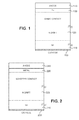
- FIGs. 1 and 2 show a conventional PIN diode and a conventional Schottky rectifier, respectively.
- the PIN diode includes a highly doped semiconductor substrate 110 that is heavily doped with a dopant of a first conductivity type (e.g., n+ type).
- An epitaxial drift layer 120 is formed on the substrate 110 and is more lightly doped with a dopant of the first conductivity type (e.g., n- type).
- a heavily doped ohmic contact layer 130 is formed on the drift layer 120.
- the contact layer 130 is heavily doped with a dopant of the second conductivity type (e.g., p+ type).
- a cathode electrode 150 is formed on the backside of the substrate 110 and an anode metal 140 is formed over the ohmic contact layer 130.
- the conventional Schottky rectifier shown in FIG. 2 includes a highly doped substrate 210 that is heavily doped with a dopant of a first conductivity type (e.g., n+ type). Similar to the PIN diode, a drift layer 220 is formed on the substrate 210 and is more lightly doped with a dopant of the first conductivity type (e.g., n- type). Then, instead of an ohmic contact layer, a metal layer 230 is formed over the drift layer 230. A Schottky contact is formed at the interface between the metal layer 230 and the drift layer 220. A cathode electrode 250 is formed on the backside of the substrate 210 and an anode metal 240 is formed over the metal layer 230.
- a first conductivity type e.g., n+ type
- a drift layer 220 is formed on the substrate 210 and is more lightly doped with a dopant of the first conductivity type (e.g., n- type).
- TMBS Trench MOS Barrier Schottky
- This device features multiple trench MOS cells in its active region to reduce the surface electric field and create a lateral barrier which opposes the flow of the leakage currents. As a result the off-state leakage currents are significantly reduced.
- the MOS trenches also act as field plates and thus allow for a slight increase in the doping of the drift region without compromising the breakdown.
- the on-state voltage drop of the TMBS device remains an issue in high voltage applications, where the breakdown is in excess of 300V. This is because the unipolar conduction mechanism of the Schottky rectifier is not as effective as the bipolar conduction specific to PIN type diodes.
- EP2187441 discloses a switching device comprising a Schottky barrier.
- a semiconductor rectifier according to claim 1 is provided.
- a Schottky diode or rectifier device which, like conventional Schottky diodes, offers fast speed and low switching losses, but with a higher current capability and considerably lower on-state losses.
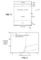
- FIG. 3 shows one example of a Schottky diode constructed not in accordance with the present invention.
- the Schottky diode 300 includes a highly doped substrate 310 that is heavily doped with a dopant of a first conductivity type (e.g., n+ type).
- An epitaxial drift layer 320 is formed on the substrate 310 and is more lightly doped with a dopant of the first conductivity type (e.g., n- type).
- a lightly doped layer 330 of the second conductivity type (e.g., p- type) is formed over the drift layer 320.
- the lightly doped layer from time to time will be referred to as a transparent layer.
- a metal layer 340 which is formed from a metal (e.g., nickel) capable of forming a silicide is deposited. Once the silicide has been formed, the metal which has not reacted with the semiconductor material is removed by a selective etch.
- a cathode electrode 350 is formed on the backside of the substrate 310 and an anode metal 360 is formed over the metal layer 340.
- the so-called transparent layer 330 forms a Schottky contact with the metallization at its surface and a low injection efficiency junction at the interface with the n-type drift layer 320.
- this device has a mixed bipolar and unipolar conduction controlled by the p- transparent layer/n- drift layer injection and the Schottky barrier, respectively.
- the diode 300 has a substantially lower on-state resistance and leakage current compared to a conventional Schottky rectifier, while offering significantly faster speed and lower losses during the reverse recovery of the diode.
- FIG. 4 shows graphs of the typical on-state characteristics of (a) conventional PIN diode, (b) a conventional Schottky rectifier and (c) the Schottky diode 300 not in accordance with the present invention.
- the graphs demonstrate that the diode 300 has different bends in its characteristics (due to different areas where the bipolar conduction and the Schottky limited conduction take place) and offers a significantly improved on-state capability compared to a conventional Schottky rectifier.
- FIG. 5 shows a schematic of the typical reverse recovery characteristics of (a) a conventional PIN diode, (b) a conventional Schottky rectifier and (c) the Schottky diode 300 not in accordance with the present invention.
- the PIN diode which features a p+ injection layer and an anode Ohmic contact, suffers from exceedingly high reverse leakage current, high losses and slow speeds.
- the Schottky diode on the other hand, being a unipolar device, offers fast speed and low switching losses.
- the device 300 not according to this invention is closer to the Schottky diode in terms of speed and losses but (as shown in FIG. 4 ) still preserves higher current capability and considerably lower on-state losses than the Schottky rectifier.
- the transparent layer 330 which injects minority carriers (holes) in the drift region and allows formation of a plasma (excess of electrons and holes in quasi-neutrality equilibrium, in concentrations above the doping level).
- the injection of the plasma is limited by the Schottky contact and further controlled by the 'transparency' of the transparent layer 330.
- the transparent layer 300 By making the transparent layer 300 more lightly doped, the transparency increases, allowing a higher fraction of electron current to penetrate through it and reach the anode contact. This results in less plasma formation in the on-state and, as a result, a faster reverse recovery response.
- the plasma level can be increased with a further increase in the on-state performance, though at the expense of increased switching losses. This trade-off will be further discussed at a later point below.
- a Schottky rectifier is provided which is based on the previously mentioned Trench MOS Barrier Schottky (TMBS) design.
- TMBS Trench MOS Barrier Schottky
- This device features multiple trench MOS cells in its active region to reduce the surface electric field and create a lateral barrier which opposes the flow of the leakage currents.
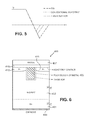
- FIG. 6 One example of this example is shown in FIG. 6 .
- the TMBS diode 400 of FIG. 6 includes a heavily-doped n-type semiconductor wafer 401 on which is formed a lightly-doped n-type epitaxial layer 402. Openings are formed in this epitaxial layer, which may be, for example, trench-shaped. Conductive regions 403 are formed in the openings, which are made, for example, of doped polysilicon. An insulating layer 404 is interposed between each conductive region and the walls of the corresponding opening (e.g., trench). The insulating layer 404 may be formed, for example, by thermal oxidation and the opening may be filled with polysilicon by conformal deposition, followed by a planarization step.
- Transparent regions 410 can then be formed by using, for example, an implantation or diffusion technique.
- the transparent regions are formed by implantation, followed by rapid annealing and possibly a light drive-in to control the dosage and junction depth of the transparent regions 410.
- the doping concentration (or the charge dosage) of the transparent regions 410 can be suitably adjusted to determine the appropriate trade-off between the on-state voltage and the turn-off energy losses.
- a metal for example, nickel, capable of forming a silicide layer 415 above the epitaxial layer 402 and above the polysilicon filled areas in the trench, is deposited. Once the silicide has been formed, the metal which has not reacted with the semiconductor material is removed by selective etch. After this, an anode metal 407 is formed on the upper surface side over the metal layer 415 and a cathode metal 408 is formed on the lower surface side of the substrate 401.
- FIG. 7 shows the simulated output characteristics of the p-TMBS device for different implantation dosages in the transparent regions 410.
- the on-state voltage drop at a current density of 250 A/cm 2 i.e. the operating current density
- the effect of increasing the doping level or the dosage in the transparent layer is that the injection efficiency of the p- transparent layer/n-drift region is increased, or the transparency is reduced.
- V bi KT q ln N d N a n i 2
- K Bolztmann constant
- T temperature on the Kelvin scale
- q electron charge
- N d electron density on the N side
- N a the hole density on the P side.
- the excess minority carrier (excess hole) distribution profiles of the p-TMBS device for different p-type implantation dosages are shown in FIG. 8 .
- the excess hole concentration (equivalent to plasma) increases with the p-type implantation dosage in the transparent layer, and this is the reason why the on-state voltage varies with the dosage level.
- case D whose p-type dosage is the highest, has the largest excess hole concentration, in particular in the middle of the drift region. It has been known that the excess carriers in the middle area are the last to be removed during transient operation, and hence the fewer holes in this area, the faster the turn-off switching speed.
- the implantation dosage is 1x10 15 cm -2 for case D, and this should be regarded as a p+ implant, rather than p- implant.
- the device is virtually a PIN diode, since, due to tunnelling, the contact is no longer Schottky but Ohmic.
- FIG. 9 is a schematic diagram of the current waveforms at turn-off transient. It shows that the higher the implantation dosage, the longer the turn-off time. However, if the carrier concentration in the drift region is very low (as in case A, for example) then the conductivity modulation effect is trivial and the on-state voltage is found to be more than 1.5 V at a current density 250 A/cm 2 (see FIG. 7 ).
- the presence of the p-transparent layer under the Schottky contact also helps to reduce the reverse leakage currents, as shown in FIG. 10 , which illustrates the off-state blocking characteristics of the device.
- FIG. 10 illustrates the off-state blocking characteristics of the device.
- the existence of a PN junction at the anode electrode enhances the immunity of the Schottky contact against the barrier lowering effect at high electric field. Therefore, it can be seen that the device without any p-type implantation has the highest leakage current.
- the other devices even when the p-transparent layer implantation dosage is the lowest, show the advantage of reducing reverse leakage current significantly.
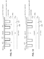
- FIG. 11 shows that the transparent layer 410 (doped p- type in this example) is only inserted in some parts (e.g. sections/areas/cells) of the device.
- the transparent layer 410 is only located between some pairs of adjacent MOS trenches, but not other pairs.
- a conventional TMBS is present in other parts of the device that do not include the transparent layer.
- the structure is effectively an integrated transparent Schottky diode in parallel with a conventional TMBS.
- FIG. 12 is a variation of FIG. 11 where the trenches are only present in the conventional TMBS cells, while the transparent layer 410 is present as a planar structure in the rest of the active area of the device.
- the transparent layer shown in the embodiment of FIG. 6 is arranged as regions around the trenches.
- the transparent layer can be formed by ion implantation and/or diffusion techniques using a suitable p-type dopant.
- the implantation energy may be kept low (e.g., 25 KeV).
- the implantation step may be followed by an annealing step (e.g., for 60 minutes at a temperature of 950°C so that the semiconductor surface remains sufficiently smooth to form a quality Schottky contact.
- an annealing step e.g., for 60 minutes at a temperature of 950°C so that the semiconductor surface remains sufficiently smooth to form a quality Schottky contact.
- geometrical dimensions and conductivities of the main layers in the structure are given below:
Landscapes
- Electrodes Of Semiconductors (AREA)
Applications Claiming Priority (3)
| Application Number | Priority Date | Filing Date | Title |
|---|---|---|---|
| US40529310P | 2010-10-21 | 2010-10-21 | |
| US13/222,249 US8816468B2 (en) | 2010-10-21 | 2011-08-31 | Schottky rectifier |
| PCT/US2011/057012 WO2012054682A2 (en) | 2010-10-21 | 2011-10-20 | Improved schottky rectifier |
Publications (3)
| Publication Number | Publication Date |
|---|---|
| EP2630663A2 EP2630663A2 (en) | 2013-08-28 |
| EP2630663A4 EP2630663A4 (en) | 2014-10-01 |
| EP2630663B1 true EP2630663B1 (en) | 2016-10-19 |
Family
ID=45972289
Family Applications (1)
| Application Number | Title | Priority Date | Filing Date |
|---|---|---|---|
| EP11835119.6A Active EP2630663B1 (en) | 2010-10-21 | 2011-10-20 | Improved Schottky rectifier and method of fabricating thereof |
Country Status (7)
| Country | Link |
|---|---|
| US (2) | US8816468B2 (enExample) |
| EP (1) | EP2630663B1 (enExample) |
| JP (2) | JP5989652B2 (enExample) |
| KR (1) | KR101987009B1 (enExample) |
| CN (1) | CN103180961B (enExample) |
| TW (1) | TWI566422B (enExample) |
| WO (1) | WO2012054682A2 (enExample) |
Families Citing this family (32)
| Publication number | Priority date | Publication date | Assignee | Title |
|---|---|---|---|---|
| CN103378177B (zh) * | 2012-04-30 | 2017-04-26 | 朱江 | 一种具有沟槽肖特基半导体装置及其制备方法 |
| JP5787853B2 (ja) * | 2012-09-12 | 2015-09-30 | 株式会社東芝 | 電力用半導体装置 |
| CN103681877A (zh) * | 2012-09-26 | 2014-03-26 | 比亚迪股份有限公司 | 一种快恢复二极管的结构及其制造方法 |
| US8981381B2 (en) | 2012-11-16 | 2015-03-17 | Vishay General Semiconductor Llc | GaN-based Schottky diode having dual metal, partially recessed electrode |
| US8981528B2 (en) | 2012-11-16 | 2015-03-17 | Vishay General Semiconductor Llc | GaN-based Schottky diode having partially recessed anode |
| US9018698B2 (en) * | 2012-11-16 | 2015-04-28 | Vishay General Semiconductor Llc | Trench-based device with improved trench protection |
| US9716151B2 (en) * | 2013-09-24 | 2017-07-25 | Semiconductor Components Industries, Llc | Schottky device having conductive trenches and a multi-concentration doping profile therebetween |
| CN104795452B (zh) * | 2014-01-16 | 2018-04-27 | 上海韦尔半导体股份有限公司 | 肖特基整流器及其制作方法 |
| CN103943688B (zh) * | 2014-04-21 | 2017-06-13 | 中航(重庆)微电子有限公司 | 一种肖特基势垒二极管器件结构及其制作方法 |
| DE102015204138A1 (de) * | 2015-03-09 | 2016-09-15 | Robert Bosch Gmbh | Halbleitervorrichtung mit einer Trench-MOS-Barrier-Schottky-Diode |
| DE102015204137A1 (de) * | 2015-03-09 | 2016-09-15 | Robert Bosch Gmbh | Halbleitervorrichtung mit einer Trench-Schottky-Barrier-Schottky-Diode |
| EP3067935A1 (en) * | 2015-03-10 | 2016-09-14 | ABB Technology AG | Power semiconductor rectifier with controllable on-state voltage |
| CN107591318B (zh) * | 2016-07-07 | 2020-08-07 | 北大方正集团有限公司 | 沟槽肖特基器件的制作方法 |
| CN106024915B (zh) * | 2016-07-25 | 2019-01-01 | 电子科技大学 | 一种超级结肖特基二极管 |
| JP6742925B2 (ja) * | 2017-01-18 | 2020-08-19 | 株式会社 日立パワーデバイス | 半導体装置、及びそれを用いた電力変換装置 |
| CN107946371B (zh) * | 2017-01-24 | 2024-04-05 | 重庆中科渝芯电子有限公司 | 一种肖特基势垒接触的超势垒整流器及其制造方法 |
| CN107946301A (zh) * | 2017-02-24 | 2018-04-20 | 重庆中科渝芯电子有限公司 | 一种肖特基势垒接触的沟槽型超势垒整流器及其制造方法 |
| CN109148605B (zh) * | 2017-06-19 | 2022-02-18 | 比亚迪半导体股份有限公司 | 快恢复二极管及制备方法、电子设备 |
| WO2019013136A1 (ja) | 2017-07-08 | 2019-01-17 | 株式会社Flosfia | 半導体装置 |
| US10424677B2 (en) * | 2017-08-31 | 2019-09-24 | Littelfuse, Inc. | Charge carrier extraction inverse diode |
| CN108010910A (zh) * | 2017-11-21 | 2018-05-08 | 重庆大学 | 一种沟槽型肖特基接触超级势垒整流器及其制作方法 |
| CN109962097A (zh) * | 2017-12-26 | 2019-07-02 | 比亚迪股份有限公司 | 二极管器件及其制造工艺 |
| CN111656532B (zh) * | 2018-02-09 | 2023-05-09 | 三菱电机株式会社 | 电力用半导体装置 |
| US10608122B2 (en) | 2018-03-13 | 2020-03-31 | Semicondutor Components Industries, Llc | Schottky device and method of manufacture |
| US10692988B2 (en) | 2018-11-26 | 2020-06-23 | Infineon Technologies Austria Ag | Semiconductor device having integrated MOS-gated or Schottky diodes |
| CN109786472A (zh) * | 2019-03-01 | 2019-05-21 | 重庆平伟实业股份有限公司 | 一种功率半导体器件 |
| CN111816693A (zh) * | 2019-04-10 | 2020-10-23 | 台湾茂矽电子股份有限公司 | 二极管结构及其制造方法 |
| TW202038473A (zh) * | 2019-04-10 | 2020-10-16 | 台灣茂矽電子股份有限公司 | 二極體結構及其製造方法 |
| US11532758B2 (en) | 2019-09-24 | 2022-12-20 | Texas Instruments Incorporated | Low leakage Schottky diode |
| CN114300543B (zh) * | 2022-03-10 | 2022-06-07 | 安建科技(深圳)有限公司 | 一种电子抽取型续流二极管器件及其制备方法 |
| CN115312591B (zh) * | 2022-10-10 | 2022-12-23 | 深圳市威兆半导体股份有限公司 | 一种快恢复二极管及其制备方法 |
| KR102905044B1 (ko) | 2023-11-15 | 2025-12-29 | 주식회사 웨이브트랙 | 고출력 고주파 입력 신호 내성을 갖는 고주파 신호 직류 정류 회로 |
Family Cites Families (26)
| Publication number | Priority date | Publication date | Assignee | Title |
|---|---|---|---|---|
| JPS51120674A (en) * | 1975-04-16 | 1976-10-22 | Hitachi Ltd | Semiconductor device |
| JP2590284B2 (ja) | 1990-02-28 | 1997-03-12 | 株式会社日立製作所 | 半導体装置及びその製造方法 |
| JPH0590565A (ja) | 1991-09-25 | 1993-04-09 | Shindengen Electric Mfg Co Ltd | 整流用半導体装置 |
| JP2835544B2 (ja) * | 1991-10-15 | 1998-12-14 | 新電元工業株式会社 | 整流用半導体装置 |
| JPH0878702A (ja) * | 1994-09-01 | 1996-03-22 | Fuji Electric Co Ltd | 半導体装置 |
| FR2764117B1 (fr) * | 1997-05-30 | 1999-08-13 | Sgs Thomson Microelectronics | Contact sur une region de type p |
| JP3618517B2 (ja) * | 1997-06-18 | 2005-02-09 | 三菱電機株式会社 | 半導体装置およびその製造方法 |
| US6252288B1 (en) | 1999-01-19 | 2001-06-26 | Rockwell Science Center, Llc | High power trench-based rectifier with improved reverse breakdown characteristic |
| JP2000216410A (ja) * | 1999-01-22 | 2000-08-04 | Hitachi Ltd | ショットキ―バリアダイオ―ドの製造方法 |
| US6191447B1 (en) | 1999-05-28 | 2001-02-20 | Micro-Ohm Corporation | Power semiconductor devices that utilize tapered trench-based insulating regions to improve electric field profiles in highly doped drift region mesas and methods of forming same |
| JP4118459B2 (ja) * | 1999-07-09 | 2008-07-16 | 富士電機デバイステクノロジー株式会社 | ショットキーバリアダイオード |
| JP2001068688A (ja) * | 1999-08-26 | 2001-03-16 | Fuji Electric Co Ltd | ショットキーバリアダイオードの製造方法およびショットキーバリアダイオード |
| JP3691736B2 (ja) * | 2000-07-31 | 2005-09-07 | 新電元工業株式会社 | 半導体装置 |
| US6846729B2 (en) | 2001-10-01 | 2005-01-25 | International Rectifier Corporation | Process for counter doping N-type silicon in Schottky device Ti silicide barrier |
| JP3858693B2 (ja) * | 2001-12-28 | 2006-12-20 | サンケン電気株式会社 | 半導体素子の製造方法 |
| US6998694B2 (en) | 2003-08-05 | 2006-02-14 | Shye-Lin Wu | High switching speed two mask Schottky diode with high field breakdown |
| JP2005243717A (ja) * | 2004-02-24 | 2005-09-08 | Sanyo Electric Co Ltd | 半導体装置 |
| US7078780B2 (en) * | 2004-04-19 | 2006-07-18 | Shye-Lin Wu | Schottky barrier diode and method of making the same |
| DE102004059640A1 (de) | 2004-12-10 | 2006-06-22 | Robert Bosch Gmbh | Halbleitereinrichtung und Verfahren zu deren Herstellung |
| JP4793905B2 (ja) * | 2005-03-24 | 2011-10-12 | 日本碍子株式会社 | 半導体装置およびその製造方法 |
| JP5351519B2 (ja) | 2005-12-27 | 2013-11-27 | パワー・インテグレーションズ・インコーポレーテッド | 高速回復整流器構造体の装置および方法 |
| US7709864B2 (en) * | 2006-04-07 | 2010-05-04 | Diodes Fabtech Inc | High-efficiency Schottky rectifier and method of manufacturing same |
| JP4930904B2 (ja) * | 2007-09-07 | 2012-05-16 | サンケン電気株式会社 | 電気回路のスイッチング装置 |
| US20090309181A1 (en) * | 2008-06-12 | 2009-12-17 | Force Mos Technology Co. Ltd. | Trench schottky with multiple epi structure |
| US7750412B2 (en) * | 2008-08-06 | 2010-07-06 | Fairchild Semiconductor Corporation | Rectifier with PN clamp regions under trenches |
| US8049276B2 (en) * | 2009-06-12 | 2011-11-01 | Fairchild Semiconductor Corporation | Reduced process sensitivity of electrode-semiconductor rectifiers |
-
2011
- 2011-08-31 US US13/222,249 patent/US8816468B2/en active Active
- 2011-10-18 TW TW100137738A patent/TWI566422B/zh active
- 2011-10-20 CN CN201180050938.9A patent/CN103180961B/zh active Active
- 2011-10-20 KR KR1020137012458A patent/KR101987009B1/ko active Active
- 2011-10-20 WO PCT/US2011/057012 patent/WO2012054682A2/en not_active Ceased
- 2011-10-20 JP JP2013535073A patent/JP5989652B2/ja active Active
- 2011-10-20 EP EP11835119.6A patent/EP2630663B1/en active Active
-
2014
- 2014-08-14 US US14/459,599 patent/US20140357059A1/en not_active Abandoned
-
2016
- 2016-08-08 JP JP2016155375A patent/JP6471126B2/ja active Active
Non-Patent Citations (1)
| Title |
|---|
| None * |
Also Published As
| Publication number | Publication date |
|---|---|
| EP2630663A2 (en) | 2013-08-28 |
| JP5989652B2 (ja) | 2016-09-07 |
| KR20130093126A (ko) | 2013-08-21 |
| CN103180961A (zh) | 2013-06-26 |
| JP2013545295A (ja) | 2013-12-19 |
| TWI566422B (zh) | 2017-01-11 |
| WO2012054682A2 (en) | 2012-04-26 |
| EP2630663A4 (en) | 2014-10-01 |
| US20140357059A1 (en) | 2014-12-04 |
| TW201238059A (en) | 2012-09-16 |
| US8816468B2 (en) | 2014-08-26 |
| JP6471126B2 (ja) | 2019-02-13 |
| US20120098082A1 (en) | 2012-04-26 |
| JP2016197753A (ja) | 2016-11-24 |
| KR101987009B1 (ko) | 2019-06-10 |
| WO2012054682A3 (en) | 2012-06-21 |
| CN103180961B (zh) | 2016-02-17 |
Similar Documents
| Publication | Publication Date | Title |
|---|---|---|
| EP2630663B1 (en) | Improved Schottky rectifier and method of fabricating thereof | |
| US8198687B2 (en) | Structure with PN clamp regions under trenches | |
| EP2920816B1 (en) | Method of manufacturing trench-based schottky diode with improved trench protection | |
| US7186609B2 (en) | Method of fabricating trench junction barrier rectifier | |
| US6710418B1 (en) | Schottky rectifier with insulation-filled trenches and method of forming the same | |
| EP4500597A1 (en) | Support shield structures for trenched semiconductor devices | |
| JP3895402B2 (ja) | 半導体デバイス | |
| CN107403830A (zh) | 半导体器件及其制造 | |
| CN105810754A (zh) | 一种具有积累层的金属氧化物半导体二极管 | |
| US10304971B2 (en) | High speed Schottky rectifier | |
| GB2622268A (en) | Silicon carbide lateral power semiconductor device | |
| US10177232B2 (en) | Methods for manufacturing a Schottky device with mesa regions in-between conductive trenches and having multi-concentration doping profiles | |
| KR20140092209A (ko) | 반도체 전력 정류 장치 | |
| WO2025066130A1 (zh) | 一种SiC功率MOS器件及其制备方法 | |
| CN105957900A (zh) | 一种具有高耐压低导通压降特性的金属氧化物二极管 |
Legal Events
| Date | Code | Title | Description |
|---|---|---|---|
| PUAI | Public reference made under article 153(3) epc to a published international application that has entered the european phase |
Free format text: ORIGINAL CODE: 0009012 |
|
| 17P | Request for examination filed |
Effective date: 20130521 |
|
| AK | Designated contracting states |
Kind code of ref document: A2 Designated state(s): AL AT BE BG CH CY CZ DE DK EE ES FI FR GB GR HR HU IE IS IT LI LT LU LV MC MK MT NL NO PL PT RO RS SE SI SK SM TR |
|
| DAX | Request for extension of the european patent (deleted) | ||
| A4 | Supplementary search report drawn up and despatched |
Effective date: 20140828 |
|
| RIC1 | Information provided on ipc code assigned before grant |
Ipc: H01L 29/872 20060101AFI20140822BHEP Ipc: H01L 21/329 20060101ALI20140822BHEP Ipc: H01L 29/868 20060101ALI20140822BHEP |
|
| GRAP | Despatch of communication of intention to grant a patent |
Free format text: ORIGINAL CODE: EPIDOSNIGR1 |
|
| INTG | Intention to grant announced |
Effective date: 20160803 |
|
| GRAS | Grant fee paid |
Free format text: ORIGINAL CODE: EPIDOSNIGR3 |
|
| GRAA | (expected) grant |
Free format text: ORIGINAL CODE: 0009210 |
|
| AK | Designated contracting states |
Kind code of ref document: B1 Designated state(s): AL AT BE BG CH CY CZ DE DK EE ES FI FR GB GR HR HU IE IS IT LI LT LU LV MC MK MT NL NO PL PT RO RS SE SI SK SM TR |
|
| REG | Reference to a national code |
Ref country code: GB Ref legal event code: FG4D |
|
| REG | Reference to a national code |
Ref country code: CH Ref legal event code: EP |
|
| REG | Reference to a national code |
Ref country code: AT Ref legal event code: REF Ref document number: 838989 Country of ref document: AT Kind code of ref document: T Effective date: 20161115 |
|
| REG | Reference to a national code |
Ref country code: IE Ref legal event code: FG4D |
|
| REG | Reference to a national code |
Ref country code: FR Ref legal event code: PLFP Year of fee payment: 6 |
|
| REG | Reference to a national code |
Ref country code: DE Ref legal event code: R096 Ref document number: 602011031559 Country of ref document: DE |
|
| REG | Reference to a national code |
Ref country code: NL Ref legal event code: MP Effective date: 20161019 |
|
| REG | Reference to a national code |
Ref country code: LT Ref legal event code: MG4D |
|
| PG25 | Lapsed in a contracting state [announced via postgrant information from national office to epo] |
Ref country code: BE Free format text: LAPSE BECAUSE OF NON-PAYMENT OF DUE FEES Effective date: 20161031 Ref country code: LV Free format text: LAPSE BECAUSE OF FAILURE TO SUBMIT A TRANSLATION OF THE DESCRIPTION OR TO PAY THE FEE WITHIN THE PRESCRIBED TIME-LIMIT Effective date: 20161019 |
|
| REG | Reference to a national code |
Ref country code: AT Ref legal event code: MK05 Ref document number: 838989 Country of ref document: AT Kind code of ref document: T Effective date: 20161019 |
|
| PG25 | Lapsed in a contracting state [announced via postgrant information from national office to epo] |
Ref country code: NO Free format text: LAPSE BECAUSE OF FAILURE TO SUBMIT A TRANSLATION OF THE DESCRIPTION OR TO PAY THE FEE WITHIN THE PRESCRIBED TIME-LIMIT Effective date: 20170119 Ref country code: SE Free format text: LAPSE BECAUSE OF FAILURE TO SUBMIT A TRANSLATION OF THE DESCRIPTION OR TO PAY THE FEE WITHIN THE PRESCRIBED TIME-LIMIT Effective date: 20161019 Ref country code: GR Free format text: LAPSE BECAUSE OF FAILURE TO SUBMIT A TRANSLATION OF THE DESCRIPTION OR TO PAY THE FEE WITHIN THE PRESCRIBED TIME-LIMIT Effective date: 20170120 Ref country code: LT Free format text: LAPSE BECAUSE OF FAILURE TO SUBMIT A TRANSLATION OF THE DESCRIPTION OR TO PAY THE FEE WITHIN THE PRESCRIBED TIME-LIMIT Effective date: 20161019 |
|
| PG25 | Lapsed in a contracting state [announced via postgrant information from national office to epo] |
Ref country code: FI Free format text: LAPSE BECAUSE OF FAILURE TO SUBMIT A TRANSLATION OF THE DESCRIPTION OR TO PAY THE FEE WITHIN THE PRESCRIBED TIME-LIMIT Effective date: 20161019 Ref country code: AT Free format text: LAPSE BECAUSE OF FAILURE TO SUBMIT A TRANSLATION OF THE DESCRIPTION OR TO PAY THE FEE WITHIN THE PRESCRIBED TIME-LIMIT Effective date: 20161019 Ref country code: NL Free format text: LAPSE BECAUSE OF FAILURE TO SUBMIT A TRANSLATION OF THE DESCRIPTION OR TO PAY THE FEE WITHIN THE PRESCRIBED TIME-LIMIT Effective date: 20161019 Ref country code: BE Free format text: LAPSE BECAUSE OF FAILURE TO SUBMIT A TRANSLATION OF THE DESCRIPTION OR TO PAY THE FEE WITHIN THE PRESCRIBED TIME-LIMIT Effective date: 20161019 Ref country code: ES Free format text: LAPSE BECAUSE OF FAILURE TO SUBMIT A TRANSLATION OF THE DESCRIPTION OR TO PAY THE FEE WITHIN THE PRESCRIBED TIME-LIMIT Effective date: 20161019 Ref country code: PT Free format text: LAPSE BECAUSE OF FAILURE TO SUBMIT A TRANSLATION OF THE DESCRIPTION OR TO PAY THE FEE WITHIN THE PRESCRIBED TIME-LIMIT Effective date: 20170220 Ref country code: RS Free format text: LAPSE BECAUSE OF FAILURE TO SUBMIT A TRANSLATION OF THE DESCRIPTION OR TO PAY THE FEE WITHIN THE PRESCRIBED TIME-LIMIT Effective date: 20161019 Ref country code: PL Free format text: LAPSE BECAUSE OF FAILURE TO SUBMIT A TRANSLATION OF THE DESCRIPTION OR TO PAY THE FEE WITHIN THE PRESCRIBED TIME-LIMIT Effective date: 20161019 Ref country code: HR Free format text: LAPSE BECAUSE OF FAILURE TO SUBMIT A TRANSLATION OF THE DESCRIPTION OR TO PAY THE FEE WITHIN THE PRESCRIBED TIME-LIMIT Effective date: 20161019 Ref country code: IS Free format text: LAPSE BECAUSE OF FAILURE TO SUBMIT A TRANSLATION OF THE DESCRIPTION OR TO PAY THE FEE WITHIN THE PRESCRIBED TIME-LIMIT Effective date: 20170219 |
|
| REG | Reference to a national code |
Ref country code: CH Ref legal event code: PL |
|
| REG | Reference to a national code |
Ref country code: DE Ref legal event code: R097 Ref document number: 602011031559 Country of ref document: DE |
|
| REG | Reference to a national code |
Ref country code: IE Ref legal event code: MM4A |
|
| PG25 | Lapsed in a contracting state [announced via postgrant information from national office to epo] |
Ref country code: RO Free format text: LAPSE BECAUSE OF FAILURE TO SUBMIT A TRANSLATION OF THE DESCRIPTION OR TO PAY THE FEE WITHIN THE PRESCRIBED TIME-LIMIT Effective date: 20161019 Ref country code: MC Free format text: LAPSE BECAUSE OF FAILURE TO SUBMIT A TRANSLATION OF THE DESCRIPTION OR TO PAY THE FEE WITHIN THE PRESCRIBED TIME-LIMIT Effective date: 20161019 Ref country code: CH Free format text: LAPSE BECAUSE OF NON-PAYMENT OF DUE FEES Effective date: 20161031 Ref country code: CZ Free format text: LAPSE BECAUSE OF FAILURE TO SUBMIT A TRANSLATION OF THE DESCRIPTION OR TO PAY THE FEE WITHIN THE PRESCRIBED TIME-LIMIT Effective date: 20161019 Ref country code: LI Free format text: LAPSE BECAUSE OF NON-PAYMENT OF DUE FEES Effective date: 20161031 Ref country code: DK Free format text: LAPSE BECAUSE OF FAILURE TO SUBMIT A TRANSLATION OF THE DESCRIPTION OR TO PAY THE FEE WITHIN THE PRESCRIBED TIME-LIMIT Effective date: 20161019 Ref country code: SK Free format text: LAPSE BECAUSE OF FAILURE TO SUBMIT A TRANSLATION OF THE DESCRIPTION OR TO PAY THE FEE WITHIN THE PRESCRIBED TIME-LIMIT Effective date: 20161019 Ref country code: EE Free format text: LAPSE BECAUSE OF FAILURE TO SUBMIT A TRANSLATION OF THE DESCRIPTION OR TO PAY THE FEE WITHIN THE PRESCRIBED TIME-LIMIT Effective date: 20161019 |
|
| PLBE | No opposition filed within time limit |
Free format text: ORIGINAL CODE: 0009261 |
|
| STAA | Information on the status of an ep patent application or granted ep patent |
Free format text: STATUS: NO OPPOSITION FILED WITHIN TIME LIMIT |
|
| PG25 | Lapsed in a contracting state [announced via postgrant information from national office to epo] |
Ref country code: BG Free format text: LAPSE BECAUSE OF FAILURE TO SUBMIT A TRANSLATION OF THE DESCRIPTION OR TO PAY THE FEE WITHIN THE PRESCRIBED TIME-LIMIT Effective date: 20170119 Ref country code: SM Free format text: LAPSE BECAUSE OF FAILURE TO SUBMIT A TRANSLATION OF THE DESCRIPTION OR TO PAY THE FEE WITHIN THE PRESCRIBED TIME-LIMIT Effective date: 20161019 Ref country code: LU Free format text: LAPSE BECAUSE OF NON-PAYMENT OF DUE FEES Effective date: 20161020 |
|
| 26N | No opposition filed |
Effective date: 20170720 |
|
| PG25 | Lapsed in a contracting state [announced via postgrant information from national office to epo] |
Ref country code: IE Free format text: LAPSE BECAUSE OF NON-PAYMENT OF DUE FEES Effective date: 20161020 Ref country code: SI Free format text: LAPSE BECAUSE OF FAILURE TO SUBMIT A TRANSLATION OF THE DESCRIPTION OR TO PAY THE FEE WITHIN THE PRESCRIBED TIME-LIMIT Effective date: 20161019 |
|
| REG | Reference to a national code |
Ref country code: FR Ref legal event code: PLFP Year of fee payment: 7 |
|
| PG25 | Lapsed in a contracting state [announced via postgrant information from national office to epo] |
Ref country code: CY Free format text: LAPSE BECAUSE OF FAILURE TO SUBMIT A TRANSLATION OF THE DESCRIPTION OR TO PAY THE FEE WITHIN THE PRESCRIBED TIME-LIMIT Effective date: 20161019 Ref country code: HU Free format text: LAPSE BECAUSE OF FAILURE TO SUBMIT A TRANSLATION OF THE DESCRIPTION OR TO PAY THE FEE WITHIN THE PRESCRIBED TIME-LIMIT; INVALID AB INITIO Effective date: 20111020 |
|
| PG25 | Lapsed in a contracting state [announced via postgrant information from national office to epo] |
Ref country code: MK Free format text: LAPSE BECAUSE OF FAILURE TO SUBMIT A TRANSLATION OF THE DESCRIPTION OR TO PAY THE FEE WITHIN THE PRESCRIBED TIME-LIMIT Effective date: 20161019 Ref country code: MT Free format text: LAPSE BECAUSE OF NON-PAYMENT OF DUE FEES Effective date: 20161031 |
|
| REG | Reference to a national code |
Ref country code: FR Ref legal event code: PLFP Year of fee payment: 8 |
|
| PG25 | Lapsed in a contracting state [announced via postgrant information from national office to epo] |
Ref country code: TR Free format text: LAPSE BECAUSE OF FAILURE TO SUBMIT A TRANSLATION OF THE DESCRIPTION OR TO PAY THE FEE WITHIN THE PRESCRIBED TIME-LIMIT Effective date: 20161019 |
|
| PG25 | Lapsed in a contracting state [announced via postgrant information from national office to epo] |
Ref country code: AL Free format text: LAPSE BECAUSE OF FAILURE TO SUBMIT A TRANSLATION OF THE DESCRIPTION OR TO PAY THE FEE WITHIN THE PRESCRIBED TIME-LIMIT Effective date: 20161019 |
|
| REG | Reference to a national code |
Ref country code: DE Ref legal event code: R079 Ref document number: 602011031559 Country of ref document: DE Free format text: PREVIOUS MAIN CLASS: H01L0029872000 Ipc: H10D0008600000 |
|
| PGFP | Annual fee paid to national office [announced via postgrant information from national office to epo] |
Ref country code: IT Payment date: 20250926 Year of fee payment: 15 |
|
| PGFP | Annual fee paid to national office [announced via postgrant information from national office to epo] |
Ref country code: GB Payment date: 20250925 Year of fee payment: 15 |
|
| PGFP | Annual fee paid to national office [announced via postgrant information from national office to epo] |
Ref country code: FR Payment date: 20250930 Year of fee payment: 15 |
|
| PGFP | Annual fee paid to national office [announced via postgrant information from national office to epo] |
Ref country code: DE Payment date: 20250930 Year of fee payment: 15 |