EP2320482A2 - Hocheffiziente Leuchtdioden auf Galliumnitridbasis mit Oberflächenaufrauhung - Google Patents
Hocheffiziente Leuchtdioden auf Galliumnitridbasis mit Oberflächenaufrauhung Download PDFInfo
- Publication number
- EP2320482A2 EP2320482A2 EP11154566A EP11154566A EP2320482A2 EP 2320482 A2 EP2320482 A2 EP 2320482A2 EP 11154566 A EP11154566 A EP 11154566A EP 11154566 A EP11154566 A EP 11154566A EP 2320482 A2 EP2320482 A2 EP 2320482A2
- Authority
- EP
- European Patent Office
- Prior art keywords
- light emitting
- emitting diode
- light
- gan
- led
- Prior art date
- Legal status (The legal status is an assumption and is not a legal conclusion. Google has not performed a legal analysis and makes no representation as to the accuracy of the status listed.)
- Granted
Links
Images




Classifications
-
- H—ELECTRICITY
- H10—SEMICONDUCTOR DEVICES; ELECTRIC SOLID-STATE DEVICES NOT OTHERWISE PROVIDED FOR
- H10H—INORGANIC LIGHT-EMITTING SEMICONDUCTOR DEVICES HAVING POTENTIAL BARRIERS
- H10H20/00—Individual inorganic light-emitting semiconductor devices having potential barriers, e.g. light-emitting diodes [LED]
- H10H20/80—Constructional details
- H10H20/81—Bodies
- H10H20/822—Materials of the light-emitting regions
- H10H20/824—Materials of the light-emitting regions comprising only Group III-V materials, e.g. GaP
-
- H—ELECTRICITY
- H10—SEMICONDUCTOR DEVICES; ELECTRIC SOLID-STATE DEVICES NOT OTHERWISE PROVIDED FOR
- H10H—INORGANIC LIGHT-EMITTING SEMICONDUCTOR DEVICES HAVING POTENTIAL BARRIERS
- H10H20/00—Individual inorganic light-emitting semiconductor devices having potential barriers, e.g. light-emitting diodes [LED]
- H10H20/80—Constructional details
- H10H20/81—Bodies
- H10H20/819—Bodies characterised by their shape, e.g. curved or truncated substrates
- H10H20/82—Roughened surfaces, e.g. at the interface between epitaxial layers
-
- H—ELECTRICITY
- H10—SEMICONDUCTOR DEVICES; ELECTRIC SOLID-STATE DEVICES NOT OTHERWISE PROVIDED FOR
- H10H—INORGANIC LIGHT-EMITTING SEMICONDUCTOR DEVICES HAVING POTENTIAL BARRIERS
- H10H20/00—Individual inorganic light-emitting semiconductor devices having potential barriers, e.g. light-emitting diodes [LED]
- H10H20/01—Manufacture or treatment
- H10H20/011—Manufacture or treatment of bodies, e.g. forming semiconductor layers
- H10H20/013—Manufacture or treatment of bodies, e.g. forming semiconductor layers having light-emitting regions comprising only Group III-V materials
- H10H20/0133—Manufacture or treatment of bodies, e.g. forming semiconductor layers having light-emitting regions comprising only Group III-V materials with a substrate not being Group III-V materials
- H10H20/01335—Manufacture or treatment of bodies, e.g. forming semiconductor layers having light-emitting regions comprising only Group III-V materials with a substrate not being Group III-V materials the light-emitting regions comprising nitride materials
-
- H—ELECTRICITY
- H10—SEMICONDUCTOR DEVICES; ELECTRIC SOLID-STATE DEVICES NOT OTHERWISE PROVIDED FOR
- H10H—INORGANIC LIGHT-EMITTING SEMICONDUCTOR DEVICES HAVING POTENTIAL BARRIERS
- H10H20/00—Individual inorganic light-emitting semiconductor devices having potential barriers, e.g. light-emitting diodes [LED]
- H10H20/01—Manufacture or treatment
- H10H20/011—Manufacture or treatment of bodies, e.g. forming semiconductor layers
- H10H20/018—Bonding of wafers
-
- H—ELECTRICITY
- H10—SEMICONDUCTOR DEVICES; ELECTRIC SOLID-STATE DEVICES NOT OTHERWISE PROVIDED FOR
- H10H—INORGANIC LIGHT-EMITTING SEMICONDUCTOR DEVICES HAVING POTENTIAL BARRIERS
- H10H20/00—Individual inorganic light-emitting semiconductor devices having potential barriers, e.g. light-emitting diodes [LED]
- H10H20/80—Constructional details
- H10H20/81—Bodies
- H10H20/822—Materials of the light-emitting regions
- H10H20/824—Materials of the light-emitting regions comprising only Group III-V materials, e.g. GaP
- H10H20/825—Materials of the light-emitting regions comprising only Group III-V materials, e.g. GaP containing nitrogen, e.g. GaN
-
- H—ELECTRICITY
- H10—SEMICONDUCTOR DEVICES; ELECTRIC SOLID-STATE DEVICES NOT OTHERWISE PROVIDED FOR
- H10H—INORGANIC LIGHT-EMITTING SEMICONDUCTOR DEVICES HAVING POTENTIAL BARRIERS
- H10H20/00—Individual inorganic light-emitting semiconductor devices having potential barriers, e.g. light-emitting diodes [LED]
- H10H20/80—Constructional details
- H10H20/85—Packages
- H10H20/855—Optical field-shaping means, e.g. lenses
- H10H20/856—Reflecting means
-
- H—ELECTRICITY
- H10—SEMICONDUCTOR DEVICES; ELECTRIC SOLID-STATE DEVICES NOT OTHERWISE PROVIDED FOR
- H10H—INORGANIC LIGHT-EMITTING SEMICONDUCTOR DEVICES HAVING POTENTIAL BARRIERS
- H10H20/00—Individual inorganic light-emitting semiconductor devices having potential barriers, e.g. light-emitting diodes [LED]
- H10H20/80—Constructional details
-
- H—ELECTRICITY
- H10—SEMICONDUCTOR DEVICES; ELECTRIC SOLID-STATE DEVICES NOT OTHERWISE PROVIDED FOR
- H10H—INORGANIC LIGHT-EMITTING SEMICONDUCTOR DEVICES HAVING POTENTIAL BARRIERS
- H10H20/00—Individual inorganic light-emitting semiconductor devices having potential barriers, e.g. light-emitting diodes [LED]
- H10H20/80—Constructional details
- H10H20/81—Bodies
- H10H20/811—Bodies having quantum effect structures or superlattices, e.g. tunnel junctions
- H10H20/812—Bodies having quantum effect structures or superlattices, e.g. tunnel junctions within the light-emitting regions, e.g. having quantum confinement structures
-
- H—ELECTRICITY
- H10—SEMICONDUCTOR DEVICES; ELECTRIC SOLID-STATE DEVICES NOT OTHERWISE PROVIDED FOR
- H10H—INORGANIC LIGHT-EMITTING SEMICONDUCTOR DEVICES HAVING POTENTIAL BARRIERS
- H10H20/00—Individual inorganic light-emitting semiconductor devices having potential barriers, e.g. light-emitting diodes [LED]
- H10H20/80—Constructional details
- H10H20/85—Packages
- H10H20/851—Wavelength conversion means
-
- H—ELECTRICITY
- H10—SEMICONDUCTOR DEVICES; ELECTRIC SOLID-STATE DEVICES NOT OTHERWISE PROVIDED FOR
- H10H—INORGANIC LIGHT-EMITTING SEMICONDUCTOR DEVICES HAVING POTENTIAL BARRIERS
- H10H20/00—Individual inorganic light-emitting semiconductor devices having potential barriers, e.g. light-emitting diodes [LED]
- H10H20/80—Constructional details
- H10H20/85—Packages
- H10H20/852—Encapsulations
- H10H20/853—Encapsulations characterised by their shape
-
- H—ELECTRICITY
- H10—SEMICONDUCTOR DEVICES; ELECTRIC SOLID-STATE DEVICES NOT OTHERWISE PROVIDED FOR
- H10W—GENERIC PACKAGES, INTERCONNECTIONS, CONNECTORS OR OTHER CONSTRUCTIONAL DETAILS OF DEVICES COVERED BY CLASS H10
- H10W90/00—Package configurations
- H10W90/701—Package configurations characterised by the relative positions of pads or connectors relative to package parts
- H10W90/721—Package configurations characterised by the relative positions of pads or connectors relative to package parts of bump connectors
- H10W90/724—Package configurations characterised by the relative positions of pads or connectors relative to package parts of bump connectors between a chip and a stacked insulating package substrate, interposer or RDL
Definitions
- the invention is related to light emitting diodes, and more particularly, to highly efficient gallium nitride based light emitting diodes via surface roughening.
- Gallium nitride (GaN) based wide band gap semiconductor light emitting diodes have been available for about 10 years. The progress of LED development has brought about great changes in LED technology, with the realization of full-color LED displays, LED traffic signals, white LEDs and so on
- the first approach is increasing the internal quantum efficiency ( ⁇ i ), which is determined by crystal quality and epitaxial layer structure, while the second approach is increasing the light extraction efficiency ( ⁇ extraction ).
- a typical ⁇ i value for blue LEDs is more than 70% [2] and an ultraviolet (UV) LED grown on a low-dislocation GaN substrate has recently exhibited an ⁇ i of about 80% [3]. There is little room for improvement of these values.
- the critical angle for the light escape cone is about 23°. Assuming that light emitted from sidewalls and the backside is neglected, it is expected that approximately only 4% of the internal light can be extracted. The light outside the escape cone is reflected into the substrate and is reflected repeatedly or absorbed by active layers or electrodes, unless it escapes through the sidewalls.
- the LED structure affects how much light is emitted.
- the impact of LED structure on light extraction efficiency is best described by example. The following examples describe several types of LED structures.
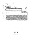
- FIG. 1 is a schematic cross-section of a conventional LED structure, which includes a p-type pad electrode 10, semitransparent electrode 12, p-type layer 14, active region 16, n-type layer 18, n-type electrode 20, and substrate 22.
- GaN is usually grown on an insulator substrate, such as sapphire
- p-type and n-type electrodes 10, 20 need to be fabricated on the same plane and the resulting device structure of the electrodes 10, 20 imposes a lateral current flow.
- the transparency of the semitransparent electrode 12 should be 100%; however, its' value for the thin metal electrodes used in GaN based LEDs is 70% at most.
- the pad electrode 10 should be formed for wire bonding, which obscures the light emitted from the inside of the LED; consequently, the extraction efficiency is expected to be quite low.
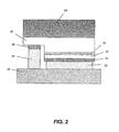
- FIG. 2 is a schematic cross-section of a flip-chip type LED structure, which includes a transparent sapphire substrate 24, n-type layer 26, n-type electrode 28, active region 30, p-type layer 32, p-type electrode 34, solder 36, and host submount 38.
- a transparent sapphire substrate 24 In order to improve the external efficiency, light can be extracted though the transparent sapphire substrate 24 of the flip-chip type LED structure.
- This method has an advantage over conventional LEDs with respect to a reduction of the light absorption by the thin metal film and the pad electrode. However, most of the light emitted from the active region would be reflected at the interface between the substrate 24 and n-type layer 26, and the interface between the substrate 24 and the air.
- LLO laser lift off'
- typical GaN-based LEDs are comprised of a thin p-GaN/active layer/n-GaN film on a sapphire or silicon carbide (SiC) substrate.
- SiC silicon carbide
- MOCVD metalorganic chemical vapor deposition
- LLO laser lift off
- a substrate-free nitrogen (N) side-up GaN-based LED structure can be made. Thereafter, an anisotropic etching process can be used to roughen the surface of the N-side-up GaN-based LED. This results in a hexagonal "cone-like" surface, which is beneficial for light extraction. Extraction efficiency of an optimally roughened surface LED shows an increase by more than 100% compared to an LED before roughening.
- GaN has been believed to be difficult to anisotropically etch. This is true because GaN is a chemically stable material compared with other semiconductor materials. The use of dry etching to make a textured surface is possible, but requires extra processing, such as photolithography, and it is impossible to make a fine cone-like surface on the GaN.
- the present invention describes a gallium nitride (GaN) based light emitting diode (LED), wherein light is extracted through a nitrogen face (N-face) of the LED and a surface of the N-face is roughened into one or more hexagonal shaped cones.
- the roughened surface reduces light reflections occurring repeatedly inside the LED, and thus extracts more light out of the LED.
- the surface of the N-face is roughened by an anisotropic etching.
- the anisotropic etching may comprise a dry etching or a photo-enhanced chemical (PEC) etching.
- the N-face GaN is prepared by a laser lift off (LLO) technique.
- the LED is grown on a c-plane GaN wafer, a p-type layer's surface is a gallium face (Ga-face), and the n-type layer's surface is a nitrogen face (N-face).
- the present invention provides a means of increasing the extraction efficiency by roughening the surface of GaN based LEDs. Specifically, applying an anisotropic PEC etching method to an N-face c-plane GaN surface results in the fabrication of cone-shaped surface features. This roughened surface reduces light reflections occurring repeatedly inside the LED, and thus extracts more light out of the LED. Moreover, the method of the present invention is simple, repeatable and should not damage the material, in contrast to other methods of surface roughening that may compromise the material's quality, all of which renders the present invention more suitable for manufacturing LEDs.
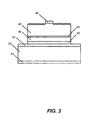
- FIG. 3 is a schematic of a surface roughened LED, which includes an n-type electrode 40, n-type layer 42, active region 44, p-type layer 46 and p-type electrode 48 which has been flip-chip bonded via a solder layer 50 to a silicon (Si) submount 52 that includes an n-type electrode 54.
- the n-type layer 42, active region 44 and p-type layer 46 are comprised of a (B, Al, Ga, In)N alloy.
- a dry or PEC etching method is used to roughen the surface of the n-type layer 42.
- Appropriate conditions such as plasma chemistries and plasma power for dry etching, and electrolytes and lamp power for PEC etching, need to be set so that a desirable surface can be obtained. It is important that this GaN based LED should be grown along its c-axis and this n-type GaN surface should be N-face because anisotropic etching can be observed on N-face GaN much more readily than Ga-face GaN.
- c-plane GaN is the structure where the plane that contains only Ga atoms and the plane that contains only N atoms are piled or stacked up alternately. If one surface is Ga-face, then the opposing surface is N-face. Due to the fact that Ga-face c-plane GaN is generally preferred from the point of view of crystal growth and device performance, N-face GaN needs to be prepared by the LLO technique, or alternatively, the LED structure could be grown on the c-plane bulk GaN wafer.
- the light emitted from the active region 44 toward the roughened n-type GaN surface 42 is scattered by the surface, which does not reflect the light back to the active region. It is desired that the p-type electrode 48 have a property of high reflection to decrease light absorption and to increase light reflection toward the n-type GaN surface 42. In experimental results, it has been determined that the present invention increases the upward light output power for the LED with a roughened surface two or three times as compared with an LED with a flat surface.
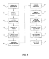
- FIG. 4 is a flowchart that illustrates the processing steps used in the preferred embodiment of the present invention.
- Block 56 represents the step of growing Ga-face epitaxial layers on a c-plane sapphire substrate by MOCVD, thereby creating a sample.
- Block 58 represents the step of annealing the sample for p-type activation, after the MOCVD.
- Block 60 represents the step of performing a p-type metallization process on the sample, including, but not limited to, silver (Ag) or aluminum (Al), to create a highly reflective p-GaN contact.
- a p-type metallization process including, but not limited to, silver (Ag) or aluminum (Al), to create a highly reflective p-GaN contact.
- Block 62 represents the step of depositing thick gold (Au) layers on the sample, followed by tin (Sn) layers as a solder metal by Sn evaporation in a thermal evaporator.
- Block 64 represents the step of flipping the sample and bonding it to an Au-coated Si substrate/submount at a temperature above 280°C, wherein an Au/Sn alloy forms that contributions to the adhesion of the sample to the Si substrate.
- Block 66 represents the step of performing an LLO process by irradiating the transparent sapphire substrate of the sample using a krypton fluoride (KrF) eximer laser light (248nm) through the backside of the sapphire substrate, resulting in local decomposition of the GaN at the GaN/sapphire substrate interface. Specifically, by rastering the KrF eximer laser spot over the sample, the GaN-based LED membrane is transferred to the Si substrate/submount.
- KrF krypton fluoride
- Block 68 represents the step of debonding the sapphire substrate from the sample, after rastering the KrF laser over the sample.
- Block 70 represents the step of removing any residual Ga droplets on the detached GaN surface of the sample using an hydrochloride (HCl) solution.
- HCl hydrochloride
- Block 72 represents the step of thinning the transferred GaN until the Si-doped N-face GaN is exposed on the sample.
- Block 74 represents the step of depositing a titanium/ aluminum/titanium/ gold (Ti/Al/Ti/Au) electrode as an n-type contact or electrode on the exposed N-face GaN of the sample.
- Block 76 represents the step of PEC etching by immersing the sample in an electrolyte solution of potassium hydroxide (KOH) and irradiating the N-face GaN surface using a xenon/mercury (Xe/Hg) lamp, in such a way that the top surface is roughened.
- KOH potassium hydroxide
- Xe/Hg xenon/mercury
- Block 78 represents the step of separating each device on the Si substrate of the sample using a dry etching, dicing or cleaving method.
- FIGS. 5(a)-(f) further illustrate the fabrication steps for the LEDs with surface roughening, wherein the LED structure includes a p-type electrode 80, GaN-based LED membrane 82, sapphire substrate 84, solder metal 86, submount (carrier) 88 and n-type electrode 90.
- FIG. 5(a) shows the results after the p-type electrode 80 deposition
- FIG. 5(b) shows the results after the LED is bonded onto the host submount 88
- FIG. 5(c) shows the results after the sapphire substrate 84 removal by LLO
- FIG. 5(d) shows the results after n-type electrode 90 deposition
- FIG. 5(e) shows the results after the roughening of the GaN surface 82
- FIG. 5(f) shows the results after device isolation.
- FIG. 6(a) shows an LED with a current-blocking layer
- FIG. 6(b) shows an LED with a current-confining frame
- the LEDs include an n-type electrode 92, n-type layer 94, active layer 96, p-type layer 98, p-type electrode 100, current-blocking layer 102, and current confining frame 104.
- the LED has a current-blocking layer 102 aligned under the n-type electrode 92.
- This current-blocking layer 102 keeps the current from concentrating below the n-type electrode 92 so that absorption of light emission under the electrode 92 can be avoided and the extraction efficiency can be increased.
- an insulator such as SiO 2 is located on the p-GaN layer 98 because the current spreading hardly occurs in the resistive p-GaN layer 98.
- the LED has a current-confining frame 104 made of an insulator. If a dry-etching or a dicing method is used to separate the devices, the sidewalls of the devices might conduct a leakage current, if the surfaces are damaged. Such leakage current decreases both the efficiency and lifetime of the LED.
- the current-confinement frame 104 contributes to the restraint of leakage current through the sidewalls of the LED and does not significantly decrease the emitting area, if the width of the frame is chosen appropriately.
- Si substrate has been described as a host submount in the LLO process, alternative substrate materials may be used to practice this invention. Although Si is cheaper and has a higher thermal conductivity than sapphire, other substrates, such as SiC, diamond, AlN, or various metals such as CuW, may be fit for use from the point of view of thermal conductivity.
- GaN devices can be also grown directly on SiC and Si substrate. If a GaN-based LED is grown on SiC or Si, conventional dry etching or wet etching can remove the substrate. By utilizing a bulk GaN substrate, the LLO process can be eliminated.
- Sample size is also an important point for LED fabrication.
- LEDs with a large size are attracting attention to meet demand for high-power LEDs.
- the resistivity of the n-type GaN is lower than that of p-GaN, the size affects the n-type electrode geometry for the purpose of current spreading.
- Ga-face epitaxial layers were grown on a c-plane sapphire substrate by MOCVD.
- the structure was comprised of 4 ⁇ m-thick undoped and Si-doped GaN layers, a 5-period GaN/InGaN multi-quantum-well (MQW), a 20nm-thick Mg-doped Al 0.2 Ga 0.8 N layer, and 0.3 ⁇ m-thick Mg-doped GaN.
- MOCVD the sample was annealed for p-type activation and then a p-type metallization process was performed.
- An Ag-based electrode was adopted as a highly reflective p-GaN contact.
- Thick Au was deposited on the sample followed by Sn evaporation in a thermal evaporator.
- the wafer was flipped and bonded to an Au-coated Si submount at a temperature of 280 °C, resulting in an alloy of Au and Sn, which contributes to firm adhesion of the wafer to the submount.
- a KrF laser (248nm) was used for the LLO process, in which the laser was shone through the transparent sapphire substrate, causing local decomposition of GaN at the boundary between GaN and sapphire. After rastering the KrF laser over the sample, the sapphire substrate was debonded. The remaining Ga droplets on the transferred GaN surface were removed by an HCl solution.
- the transferred GaN was thinned until the Si-doped GaN was exposed.
- An n-contact was formed on the exposed N-face n-GaN and each device was divided from its neighbors by reactive ion etching (RIE).
- RIE reactive ion etching
- PEC etching was used.
- a KOH solution and Xe/Hg lamp were used as electrolyte and light source, respectively.
- the output power of the LED was measured with an Si-detector set at a height of 7mm over the LED chips.
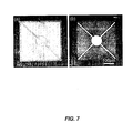
- FIGS. 7(a) and 7(b) are plan-view micrographs of an LLO-LED with a cross-shaped n-electrode, wherein the LED is bonded on an Si substrate.
- FIG. 7(a) shows the surface before roughening
- FIG. 7(b) shows the surface after roughening. Because the n-electrode blocks UV light during PEC etching, the GaN beneath it is not etched and the electrode remains on the GaN after roughening.
- a transparent electrode such as indium tin oxide (ITO) can be employed as a current spreading electrode.
- ITO indium tin oxide
- FIGS. 8(a) and 8(b) are scanning electron micrograph (SEM) images of the N-face of GaN after PEC etching for different etching times. Notice that the PEC-etched N-face GaN surfaces include a plurality of hexagonal shaped cones, which are distinct from the PEC-etched GaN surfaces reported by Youtsey, et al. [16]. This difference is considered to be due to the surface polarity of GaN. In comparing the 2 minute (min) etched surface of FIG. 8(a) and the 10 min etched surface of FIG. 8(b) , the size of the features increases and the facets of the hexagonal cones become more defined.
- SEM scanning electron micrograph
- the cone-shaped surface appears very effective for light extraction from the LED. Moreover, experimental results suggest that a cone shape can extract more light. For example, the wavelength of a blue LED in a GaN crystal is about 200 nm. If the size of the cone shape is much smaller than that value, then the light might not be affected by the roughness. On the other hand, if the size of the cone shape is close to that value, the light might be scattered or diffracted.
- the roughened surface is comprised of many hexagonal shaped cones that have an angle equal to or smaller than: 2 ⁇ sin - 1 n air / n s ⁇ 47.2 ⁇ ° for GaN, where n air is a refractive index of air and n s is a refractive index of GaN.
- the roughened surface is comprised of many hexagonal shaped cones that have an angle equal to or smaller than: 2 ⁇ sin - 1 n enc / n s for epoxy, where n enc is a refractive index of epoxy and n s is a refractive index of GaN.
- the surface may not have to be cone shaped, and a grating structure and photonic crystal should be considered. These might be better structures for light extraction.
- the fabrication of photonic crystals requires precise design and processing, which is more costly than fabricating a cone-shaped surface roughness.
- the "mirror-like" surface before PEC etching becomes discolored as the etching time increases. If a highly reflective metal is deposited on the other side of GaN film, the surface appears white; otherwise, it is darker. This is believed to be due to the light-reflection restraint at the air/GaN boundary, and if there is a highly reflective metal on the backside of the GaN, the light passing into GaN comes out again, scattering at the roughened surface.
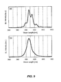
- Electroluminescence (EL) spectra from a flat-surface LED and a roughened-surface LED are shown in FIGS. 9(a) and 9(b) , respectively.
- the measurement was performed at a forward current density of 25 A/cm 2 DC at room temperature (RT).
- the spectrum of the flat-surface LED had multi-peaked emission, as shown in FIG. 9(a) , suggesting that the light emitted from the active region was interfered in the vertical GaN cavity sandwiched between mirrors made of GaN/metal and GaN/air.
- no longitudinal mode was observed on the roughened surface LED. This means that the roughened GaN/air interface scattered the light, resulting in suppression of the resonance.
- FIG. 10 is a graph of upward EL output power vs. DC injection current (L-I) characteristics for the LEDs with different etching times at room temperature. These data were obtained from the same device before and after PEC etching, so that any factor causing this difference except the surface morphology could be neglected. Any L-I curves showed linear characteristics up to 50 mA. Because of the relatively higher thermal conductivity of Si than that of sapphire, these devices are advantageous for high power operation. The output power at a given current increased with increasing PEC etching time. As compared with the output power for a flat-surface LED and the 10 min etched surface LED, this roughening treatment resulted in an increase of output power by a factor of 2.3.
- L-I DC injection current
- the power also showed a two to three-fold increase after the roughening process. Because a flat-surface LED tends to emit more light from the sidewalls of the LED chip than a roughened surface LED due to the lateral propagation of light, the difference of output power would be less if the total power were measured in an integrating sphere. Nevertheless this enhancement of extraction efficiency by anisotropic etching technique shows significant improvement.
- substrates other than sapphire or silicon carbide could be employed.
- LED structures may be created.
- RCLEDs resonant cavity LEDs
- MCLEDs micro cavity LEDs
Landscapes
- Led Devices (AREA)
- Weting (AREA)
- Drying Of Semiconductors (AREA)
Priority Applications (2)
| Application Number | Priority Date | Filing Date | Title |
|---|---|---|---|
| ES11154566.1T ES2615209T3 (es) | 2003-12-09 | 2003-12-09 | Diodos emisores de luz basados en nitruro de galio altamente eficientes por medio de una superficie convertida en rugosa |
| EP11154566.1A EP2320482B1 (de) | 2003-12-09 | 2003-12-09 | Hocheffiziente Leuchtdioden auf Galliumnitridbasis mit Oberflächenaufrauhung |
Applications Claiming Priority (3)
| Application Number | Priority Date | Filing Date | Title |
|---|---|---|---|
| EP11154566.1A EP2320482B1 (de) | 2003-12-09 | 2003-12-09 | Hocheffiziente Leuchtdioden auf Galliumnitridbasis mit Oberflächenaufrauhung |
| PCT/US2003/039211 WO2005064666A1 (en) | 2003-12-09 | 2003-12-09 | Highly efficient gallium nitride based light emitting diodes via surface roughening |
| EP03819251A EP1697983B1 (de) | 2003-12-09 | 2003-12-09 | Hocheffiziente leuchtdioden auf galliumnitridbasis mit oberflächenaufrauhung |
Related Parent Applications (2)
| Application Number | Title | Priority Date | Filing Date |
|---|---|---|---|
| EP03819251A Division EP1697983B1 (de) | 2003-12-09 | 2003-12-09 | Hocheffiziente leuchtdioden auf galliumnitridbasis mit oberflächenaufrauhung |
| EP03819251.4 Division | 2003-12-09 |
Publications (3)
| Publication Number | Publication Date |
|---|---|
| EP2320482A2 true EP2320482A2 (de) | 2011-05-11 |
| EP2320482A3 EP2320482A3 (de) | 2011-09-07 |
| EP2320482B1 EP2320482B1 (de) | 2016-11-16 |
Family
ID=34738256
Family Applications (2)
| Application Number | Title | Priority Date | Filing Date |
|---|---|---|---|
| EP03819251A Expired - Lifetime EP1697983B1 (de) | 2003-12-09 | 2003-12-09 | Hocheffiziente leuchtdioden auf galliumnitridbasis mit oberflächenaufrauhung |
| EP11154566.1A Expired - Lifetime EP2320482B1 (de) | 2003-12-09 | 2003-12-09 | Hocheffiziente Leuchtdioden auf Galliumnitridbasis mit Oberflächenaufrauhung |
Family Applications Before (1)
| Application Number | Title | Priority Date | Filing Date |
|---|---|---|---|
| EP03819251A Expired - Lifetime EP1697983B1 (de) | 2003-12-09 | 2003-12-09 | Hocheffiziente leuchtdioden auf galliumnitridbasis mit oberflächenaufrauhung |
Country Status (9)
| Country | Link |
|---|---|
| US (6) | US7704763B2 (de) |
| EP (2) | EP1697983B1 (de) |
| JP (1) | JP5719493B2 (de) |
| KR (2) | KR101154494B1 (de) |
| CN (1) | CN100521120C (de) |
| AU (1) | AU2003296426A1 (de) |
| DE (1) | DE60341314C5 (de) |
| ES (1) | ES2615209T3 (de) |
| WO (1) | WO2005064666A1 (de) |
Cited By (1)
| Publication number | Priority date | Publication date | Assignee | Title |
|---|---|---|---|---|
| EP1759424B1 (de) * | 2004-05-06 | 2019-05-01 | Cree, Inc. | Abhebeprozess für auf siliziumkarbid-substraten ausgebildete gan-filme |
Families Citing this family (242)
| Publication number | Priority date | Publication date | Assignee | Title |
|---|---|---|---|---|
| US8545629B2 (en) | 2001-12-24 | 2013-10-01 | Crystal Is, Inc. | Method and apparatus for producing large, single-crystals of aluminum nitride |
| US7638346B2 (en) * | 2001-12-24 | 2009-12-29 | Crystal Is, Inc. | Nitride semiconductor heterostructures and related methods |
| US20060005763A1 (en) * | 2001-12-24 | 2006-01-12 | Crystal Is, Inc. | Method and apparatus for producing large, single-crystals of aluminum nitride |
| US7344903B2 (en) * | 2003-09-17 | 2008-03-18 | Luminus Devices, Inc. | Light emitting device processes |
| US7341880B2 (en) * | 2003-09-17 | 2008-03-11 | Luminus Devices, Inc. | Light emitting device processes |
| WO2005029573A1 (en) | 2003-09-19 | 2005-03-31 | Tinggi Technologies Private Limited | Fabrication of semiconductor devices |
| US7704763B2 (en) | 2003-12-09 | 2010-04-27 | The Regents Of The University Of California | Highly efficient group-III nitride based light emitting diodes via fabrication of structures on an N-face surface |
| JP2007535804A (ja) | 2004-03-15 | 2007-12-06 | ティンギ テクノロジーズ プライベート リミテッド | 半導体デバイスの製造 |
| US20050205883A1 (en) * | 2004-03-19 | 2005-09-22 | Wierer Jonathan J Jr | Photonic crystal light emitting device |
| KR100568297B1 (ko) * | 2004-03-30 | 2006-04-05 | 삼성전기주식회사 | 질화물 반도체 발광 소자 및 그 제조 방법 |
| WO2005098974A1 (en) | 2004-04-07 | 2005-10-20 | Tinggi Technologies Private Limited | Fabrication of reflective layer on semiconductor light emitting diodes |
| US8035113B2 (en) | 2004-04-15 | 2011-10-11 | The Trustees Of Boston University | Optical devices featuring textured semiconductor layers |
| EP1735838B1 (de) | 2004-04-15 | 2011-10-05 | Trustees of Boston University | Optische bauelemente mit texturierten halbleiterschichten |
| US7791061B2 (en) | 2004-05-18 | 2010-09-07 | Cree, Inc. | External extraction light emitting diode based upon crystallographic faceted surfaces |
| US8227820B2 (en) | 2005-02-09 | 2012-07-24 | The Regents Of The University Of California | Semiconductor light-emitting device |
| US7345298B2 (en) | 2005-02-28 | 2008-03-18 | The Regents Of The University Of California | Horizontal emitting, vertical emitting, beam shaped, distributed feedback (DFB) lasers by growth over a patterned substrate |
| US7768024B2 (en) * | 2005-12-02 | 2010-08-03 | The Regents Of The University Of California | Horizontal emitting, vertical emitting, beam shaped, distributed feedback (DFB) lasers fabricated by growth over a patterned substrate with multiple overgrowth |
| US20090023239A1 (en) * | 2004-07-22 | 2009-01-22 | Luminus Devices, Inc. | Light emitting device processes |
| US7223998B2 (en) | 2004-09-10 | 2007-05-29 | The Regents Of The University Of California | White, single or multi-color light emitting diodes by recycling guided modes |
| EP1836879A2 (de) | 2004-12-27 | 2007-09-26 | Quantum Paper, Inc. | Adressierbares und druckbares emissives display |
| US8685764B2 (en) * | 2005-01-11 | 2014-04-01 | SemiLEDs Optoelectronics Co., Ltd. | Method to make low resistance contact |
| US8871547B2 (en) * | 2005-01-11 | 2014-10-28 | SemiLEDs Optoelectronics Co., Ltd. | Method for fabricating vertical light emitting diode (VLED) structure using a laser pulse to remove a carrier substrate |
| US7335920B2 (en) * | 2005-01-24 | 2008-02-26 | Cree, Inc. | LED with current confinement structure and surface roughening |
| KR100638730B1 (ko) * | 2005-04-14 | 2006-10-30 | 삼성전기주식회사 | 수직구조 3족 질화물 발광 소자의 제조 방법 |
| JP5043835B2 (ja) * | 2005-06-17 | 2012-10-10 | ザ リージェンツ オブ ザ ユニバーシティ オブ カリフォルニア | 光電子応用のための(Al,Ga,In)NとZnOの直接ウェーハ・ボンディング構造とその作製方法 |
| KR100599012B1 (ko) * | 2005-06-29 | 2006-07-12 | 서울옵토디바이스주식회사 | 열전도성 기판을 갖는 발광 다이오드 및 그것을 제조하는방법 |
| US8674375B2 (en) * | 2005-07-21 | 2014-03-18 | Cree, Inc. | Roughened high refractive index layer/LED for high light extraction |
| JP2007067290A (ja) * | 2005-09-01 | 2007-03-15 | Matsushita Electric Ind Co Ltd | 窒化物半導体素子の製造方法及び窒化物半導体素子製造装置 |
| SG130975A1 (en) | 2005-09-29 | 2007-04-26 | Tinggi Tech Private Ltd | Fabrication of semiconductor devices for light emission |
| SG131803A1 (en) | 2005-10-19 | 2007-05-28 | Tinggi Tech Private Ltd | Fabrication of transistors |
| JP2007150259A (ja) * | 2005-11-02 | 2007-06-14 | Sharp Corp | 窒化物半導体発光素子およびその製造方法 |
| JP2009515344A (ja) | 2005-11-04 | 2009-04-09 | ザ リージェンツ オブ ザ ユニバーシティ オブ カリフォルニア | 高い光抽出効率の発光ダイオード(led) |
| KR100640497B1 (ko) * | 2005-11-24 | 2006-11-01 | 삼성전기주식회사 | 수직 구조 질화갈륨계 발광다이오드 소자 |
| US7641735B2 (en) * | 2005-12-02 | 2010-01-05 | Crystal Is, Inc. | Doped aluminum nitride crystals and methods of making them |
| JP2007165409A (ja) * | 2005-12-09 | 2007-06-28 | Rohm Co Ltd | 半導体発光素子及び半導体発光素子の製造方法 |
| KR100661602B1 (ko) * | 2005-12-09 | 2006-12-26 | 삼성전기주식회사 | 수직 구조 질화갈륨계 led 소자의 제조방법 |
| SG133432A1 (en) | 2005-12-20 | 2007-07-30 | Tinggi Tech Private Ltd | Localized annealing during semiconductor device fabrication |
| JP2007207981A (ja) * | 2006-02-01 | 2007-08-16 | Rohm Co Ltd | 窒化物半導体発光素子の製造方法 |
| KR100844722B1 (ko) | 2006-03-07 | 2008-07-07 | 엘지전자 주식회사 | 나노콘 성장방법 및 이를 이용한 발광 다이오드의제조방법 |
| CN101454487B (zh) * | 2006-03-30 | 2013-01-23 | 晶体公司 | 氮化铝块状晶体的可控掺杂方法 |
| US9034103B2 (en) | 2006-03-30 | 2015-05-19 | Crystal Is, Inc. | Aluminum nitride bulk crystals having high transparency to ultraviolet light and methods of forming them |
| JP2007300069A (ja) * | 2006-04-04 | 2007-11-15 | Toyoda Gosei Co Ltd | 発光素子、この発光素子を用いた発光装置及びこの発光素子の製造方法 |
| US7674639B2 (en) * | 2006-08-14 | 2010-03-09 | Bridgelux, Inc | GaN based LED with etched exposed surface for improved light extraction efficiency and method for making the same |
| SG140473A1 (en) * | 2006-08-16 | 2008-03-28 | Tinggi Tech Private Ltd | Improvements in external light efficiency of light emitting diodes |
| JP2008053685A (ja) * | 2006-08-23 | 2008-03-06 | Samsung Electro Mech Co Ltd | 垂直構造窒化ガリウム系発光ダイオード素子及びその製造方法 |
| SG140512A1 (en) | 2006-09-04 | 2008-03-28 | Tinggi Tech Private Ltd | Electrical current distribution in light emitting devices |
| US9111950B2 (en) * | 2006-09-28 | 2015-08-18 | Philips Lumileds Lighting Company, Llc | Process for preparing a semiconductor structure for mounting |
| KR100815225B1 (ko) * | 2006-10-23 | 2008-03-19 | 삼성전기주식회사 | 수직구조 발광다이오드 소자 및 그 제조방법 |
| TW200830593A (en) * | 2006-11-15 | 2008-07-16 | Univ California | Transparent mirrorless light emitting diode |
| EP2843716A3 (de) | 2006-11-15 | 2015-04-29 | The Regents of The University of California | Leuchtdiode mit strukturierter Phosphorumwandlungsschicht |
| US20090121250A1 (en) * | 2006-11-15 | 2009-05-14 | Denbaars Steven P | High light extraction efficiency light emitting diode (led) using glass packaging |
| WO2008060584A2 (en) * | 2006-11-15 | 2008-05-22 | The Regents Of The University Of California | High light extraction efficiency sphere led |
| JP4980701B2 (ja) * | 2006-12-01 | 2012-07-18 | 住友電工デバイス・イノベーション株式会社 | 半導体装置の製造方法 |
| TWI533351B (zh) | 2006-12-11 | 2016-05-11 | 美國加利福尼亞大學董事會 | 高效能非極性第三族氮化物光學裝置之金屬有機化學氣相沈積生長 |
| JP2010512660A (ja) * | 2006-12-11 | 2010-04-22 | ザ リージェンツ オブ ザ ユニバーシティ オブ カリフォルニア | 無極性および半極性の発光デバイス |
| WO2008073400A1 (en) | 2006-12-11 | 2008-06-19 | The Regents Of The University Of California | Transparent light emitting diodes |
| WO2008088838A1 (en) | 2007-01-17 | 2008-07-24 | Crystal Is, Inc. | Defect reduction in seeded aluminum nitride crystal growth |
| US9771666B2 (en) | 2007-01-17 | 2017-09-26 | Crystal Is, Inc. | Defect reduction in seeded aluminum nitride crystal growth |
| WO2008094464A2 (en) * | 2007-01-26 | 2008-08-07 | Crystal Is, Inc. | Thick pseudomorphic nitride epitaxial layers |
| US8080833B2 (en) * | 2007-01-26 | 2011-12-20 | Crystal Is, Inc. | Thick pseudomorphic nitride epitaxial layers |
| JP5346443B2 (ja) * | 2007-04-16 | 2013-11-20 | ローム株式会社 | 半導体発光素子およびその製造方法 |
| US20080283503A1 (en) * | 2007-05-14 | 2008-11-20 | Cheng-Yi Liu | Method of Processing Nature Pattern on Expitaxial Substrate |
| US8088220B2 (en) | 2007-05-24 | 2012-01-03 | Crystal Is, Inc. | Deep-eutectic melt growth of nitride crystals |
| US9425357B2 (en) | 2007-05-31 | 2016-08-23 | Nthdegree Technologies Worldwide Inc. | Diode for a printable composition |
| US8674593B2 (en) | 2007-05-31 | 2014-03-18 | Nthdegree Technologies Worldwide Inc | Diode for a printable composition |
| US8877101B2 (en) | 2007-05-31 | 2014-11-04 | Nthdegree Technologies Worldwide Inc | Method of manufacturing a light emitting, power generating or other electronic apparatus |
| US8809126B2 (en) | 2007-05-31 | 2014-08-19 | Nthdegree Technologies Worldwide Inc | Printable composition of a liquid or gel suspension of diodes |
| US9018833B2 (en) | 2007-05-31 | 2015-04-28 | Nthdegree Technologies Worldwide Inc | Apparatus with light emitting or absorbing diodes |
| US8889216B2 (en) | 2007-05-31 | 2014-11-18 | Nthdegree Technologies Worldwide Inc | Method of manufacturing addressable and static electronic displays |
| US8852467B2 (en) | 2007-05-31 | 2014-10-07 | Nthdegree Technologies Worldwide Inc | Method of manufacturing a printable composition of a liquid or gel suspension of diodes |
| US9534772B2 (en) | 2007-05-31 | 2017-01-03 | Nthdegree Technologies Worldwide Inc | Apparatus with light emitting diodes |
| US8456393B2 (en) * | 2007-05-31 | 2013-06-04 | Nthdegree Technologies Worldwide Inc | Method of manufacturing a light emitting, photovoltaic or other electronic apparatus and system |
| US9419179B2 (en) | 2007-05-31 | 2016-08-16 | Nthdegree Technologies Worldwide Inc | Diode for a printable composition |
| US8415879B2 (en) | 2007-05-31 | 2013-04-09 | Nthdegree Technologies Worldwide Inc | Diode for a printable composition |
| US9343593B2 (en) | 2007-05-31 | 2016-05-17 | Nthdegree Technologies Worldwide Inc | Printable composition of a liquid or gel suspension of diodes |
| US8846457B2 (en) | 2007-05-31 | 2014-09-30 | Nthdegree Technologies Worldwide Inc | Printable composition of a liquid or gel suspension of diodes |
| US8133768B2 (en) | 2007-05-31 | 2012-03-13 | Nthdegree Technologies Worldwide Inc | Method of manufacturing a light emitting, photovoltaic or other electronic apparatus and system |
| US8124991B2 (en) * | 2007-07-26 | 2012-02-28 | The Regents Of The University Of California | Light emitting diodes with a P-type surface bonded to a transparent submount to increase light extraction efficiency |
| JP2009076694A (ja) * | 2007-09-20 | 2009-04-09 | Panasonic Corp | 窒化物半導体装置およびその製造方法 |
| KR20100097179A (ko) | 2007-11-30 | 2010-09-02 | 더 리전트 오브 더 유니버시티 오브 캘리포니아 | 표면을 거칠게하여 높은 광 추출 효율을 갖는 질화물계 발광 다이오드 |
| KR20100097177A (ko) * | 2007-11-30 | 2010-09-02 | 더 리전트 오브 더 유니버시티 오브 캘리포니아 | 향상된 광 출력을 가지는 질화 갈륨 기반의 얇은 발광 다이오드 |
| US20100295075A1 (en) * | 2007-12-10 | 2010-11-25 | 3M Innovative Properties Company | Down-converted light emitting diode with simplified light extraction |
| DE102008019268A1 (de) * | 2008-02-29 | 2009-09-03 | Osram Opto Semiconductors Gmbh | Optoelektronisches Bauelement und Verfahren zur Herstellung eines optoelektronischen Bauelements |
| US8637883B2 (en) * | 2008-03-19 | 2014-01-28 | Cree, Inc. | Low index spacer layer in LED devices |
| KR101507129B1 (ko) * | 2008-03-28 | 2015-03-31 | 서울바이오시스 주식회사 | 발광 다이오드 및 그 제조방법 |
| US8343824B2 (en) * | 2008-04-29 | 2013-01-01 | International Rectifier Corporation | Gallium nitride material processing and related device structures |
| CN102089864A (zh) * | 2008-05-12 | 2011-06-08 | 加利福尼亚大学董事会 | P型半导体异质结构的光电化学刻蚀 |
| WO2009140285A1 (en) * | 2008-05-12 | 2009-11-19 | The Regents Of The University Of California | Photoelectrochemical roughening of p-side-up gan-based light emitting diodes |
| US7992332B2 (en) | 2008-05-13 | 2011-08-09 | Nthdegree Technologies Worldwide Inc. | Apparatuses for providing power for illumination of a display object |
| US8127477B2 (en) | 2008-05-13 | 2012-03-06 | Nthdegree Technologies Worldwide Inc | Illuminating display systems |
| US20090301388A1 (en) * | 2008-06-05 | 2009-12-10 | Soraa Inc. | Capsule for high pressure processing and method of use for supercritical fluids |
| US8097081B2 (en) | 2008-06-05 | 2012-01-17 | Soraa, Inc. | High pressure apparatus and method for nitride crystal growth |
| US8871024B2 (en) * | 2008-06-05 | 2014-10-28 | Soraa, Inc. | High pressure apparatus and method for nitride crystal growth |
| US9157167B1 (en) | 2008-06-05 | 2015-10-13 | Soraa, Inc. | High pressure apparatus and method for nitride crystal growth |
| US20090320745A1 (en) * | 2008-06-25 | 2009-12-31 | Soraa, Inc. | Heater device and method for high pressure processing of crystalline materials |
| WO2011044554A1 (en) | 2009-10-09 | 2011-04-14 | Soraa, Inc. | Method for synthesis of high quality large area bulk gallium based crystals |
| WO2010005914A1 (en) * | 2008-07-07 | 2010-01-14 | Soraa, Inc. | High quality large area bulk non-polar or semipolar gallium based substrates and methods |
| CN101625971B (zh) * | 2008-07-09 | 2010-12-08 | 中国科学院半导体研究所 | 利用光辅助氧化湿法刻蚀ⅲ族氮化物的方法 |
| US8430958B2 (en) * | 2008-08-07 | 2013-04-30 | Soraa, Inc. | Apparatus and method for seed crystal utilization in large-scale manufacturing of gallium nitride |
| US10036099B2 (en) | 2008-08-07 | 2018-07-31 | Slt Technologies, Inc. | Process for large-scale ammonothermal manufacturing of gallium nitride boules |
| US8979999B2 (en) * | 2008-08-07 | 2015-03-17 | Soraa, Inc. | Process for large-scale ammonothermal manufacturing of gallium nitride boules |
| US8021481B2 (en) | 2008-08-07 | 2011-09-20 | Soraa, Inc. | Process and apparatus for large-scale manufacturing of bulk monocrystalline gallium-containing nitride |
| US8633501B2 (en) | 2008-08-12 | 2014-01-21 | Epistar Corporation | Light-emitting device having a patterned surface |
| JP2010045156A (ja) * | 2008-08-12 | 2010-02-25 | Toshiba Corp | 半導体装置の製造方法 |
| US7976630B2 (en) | 2008-09-11 | 2011-07-12 | Soraa, Inc. | Large-area seed for ammonothermal growth of bulk gallium nitride and method of manufacture |
| US20100295088A1 (en) * | 2008-10-02 | 2010-11-25 | Soraa, Inc. | Textured-surface light emitting diode and method of manufacture |
| KR20110067046A (ko) * | 2008-10-09 | 2011-06-20 | 더 리전츠 오브 더 유니버시티 오브 캘리포니아 | 발광 다이오드의 칩 형상화를 위한 광전기화학 식각 |
| US8455894B1 (en) | 2008-10-17 | 2013-06-04 | Soraa, Inc. | Photonic-crystal light emitting diode and method of manufacture |
| US8878230B2 (en) * | 2010-03-11 | 2014-11-04 | Soraa, Inc. | Semi-insulating group III metal nitride and method of manufacture |
| USRE47114E1 (en) | 2008-12-12 | 2018-11-06 | Slt Technologies, Inc. | Polycrystalline group III metal nitride with getter and method of making |
| US20100147210A1 (en) * | 2008-12-12 | 2010-06-17 | Soraa, Inc. | high pressure apparatus and method for nitride crystal growth |
| US8461071B2 (en) * | 2008-12-12 | 2013-06-11 | Soraa, Inc. | Polycrystalline group III metal nitride with getter and method of making |
| US9543392B1 (en) | 2008-12-12 | 2017-01-10 | Soraa, Inc. | Transparent group III metal nitride and method of manufacture |
| US8987156B2 (en) | 2008-12-12 | 2015-03-24 | Soraa, Inc. | Polycrystalline group III metal nitride with getter and method of making |
| CN101771115B (zh) * | 2009-01-06 | 2011-11-09 | 北京大学 | 氮化镓基材料激光剥离后氮面的处理方法 |
| TW201029218A (en) * | 2009-01-16 | 2010-08-01 | Univ Nat Central | Optical diode structure and manufacturing method |
| US20110100291A1 (en) * | 2009-01-29 | 2011-05-05 | Soraa, Inc. | Plant and method for large-scale ammonothermal manufacturing of gallium nitride boules |
| US8247886B1 (en) | 2009-03-09 | 2012-08-21 | Soraa, Inc. | Polarization direction of optical devices using selected spatial configurations |
| US8299473B1 (en) | 2009-04-07 | 2012-10-30 | Soraa, Inc. | Polarized white light devices using non-polar or semipolar gallium containing materials and transparent phosphors |
| US8791499B1 (en) | 2009-05-27 | 2014-07-29 | Soraa, Inc. | GaN containing optical devices and method with ESD stability |
| US8207547B2 (en) * | 2009-06-10 | 2012-06-26 | Brudgelux, Inc. | Thin-film LED with P and N contacts electrically isolated from the substrate |
| US20100314551A1 (en) * | 2009-06-11 | 2010-12-16 | Bettles Timothy J | In-line Fluid Treatment by UV Radiation |
| US9000466B1 (en) | 2010-08-23 | 2015-04-07 | Soraa, Inc. | Methods and devices for light extraction from a group III-nitride volumetric LED using surface and sidewall roughening |
| US8400064B2 (en) * | 2009-09-09 | 2013-03-19 | Koninklijke Philips Electronics N.V. | Zener diode protection network in submount for LEDs connected in series |
| US9583678B2 (en) | 2009-09-18 | 2017-02-28 | Soraa, Inc. | High-performance LED fabrication |
| US9293644B2 (en) | 2009-09-18 | 2016-03-22 | Soraa, Inc. | Power light emitting diode and method with uniform current density operation |
| CN107256915A (zh) | 2009-09-18 | 2017-10-17 | 天空公司 | 发光二极管器件 |
| US8933644B2 (en) | 2009-09-18 | 2015-01-13 | Soraa, Inc. | LED lamps with improved quality of light |
| CN101673792B (zh) * | 2009-09-25 | 2011-09-21 | 厦门市三安光电科技有限公司 | 一种基于无掩模转移光子晶体结构的GaN基薄膜LED的制造方法 |
| US8435347B2 (en) | 2009-09-29 | 2013-05-07 | Soraa, Inc. | High pressure apparatus with stackable rings |
| JP5281536B2 (ja) * | 2009-10-09 | 2013-09-04 | スタンレー電気株式会社 | 半導体発光装置の製造方法 |
| WO2011056675A1 (en) * | 2009-11-03 | 2011-05-12 | The Regents Of The University Of California | Superluminescent diodes by crystallographic etching |
| TWI531088B (zh) * | 2009-11-13 | 2016-04-21 | 首爾偉傲世有限公司 | 具有分散式布拉格反射器的發光二極體晶片 |
| US8963178B2 (en) | 2009-11-13 | 2015-02-24 | Seoul Viosys Co., Ltd. | Light emitting diode chip having distributed bragg reflector and method of fabricating the same |
| EP2341558B1 (de) | 2009-12-30 | 2019-04-24 | IMEC vzw | Verfahren zur herstellung eines halbleiterbauelements |
| KR100993094B1 (ko) * | 2010-02-01 | 2010-11-08 | 엘지이노텍 주식회사 | 발광소자 및 발광소자 패키지 |
| US10147850B1 (en) | 2010-02-03 | 2018-12-04 | Soraa, Inc. | System and method for providing color light sources in proximity to predetermined wavelength conversion structures |
| US8905588B2 (en) | 2010-02-03 | 2014-12-09 | Sorra, Inc. | System and method for providing color light sources in proximity to predetermined wavelength conversion structures |
| US8740413B1 (en) | 2010-02-03 | 2014-06-03 | Soraa, Inc. | System and method for providing color light sources in proximity to predetermined wavelength conversion structures |
| US20110186874A1 (en) * | 2010-02-03 | 2011-08-04 | Soraa, Inc. | White Light Apparatus and Method |
| BR112012019877A2 (pt) * | 2010-02-10 | 2016-04-26 | Tenneco Automotive Operating | injetor de fluxo em redemoinho por pressão com variabilidade de fluxo reduzido e fluxo de retorno |
| JP4886869B2 (ja) * | 2010-03-03 | 2012-02-29 | 株式会社東芝 | 半導体発光素子およびその製造方法 |
| KR100969131B1 (ko) * | 2010-03-05 | 2010-07-07 | 엘지이노텍 주식회사 | 발광 소자 제조방법 |
| US8642368B2 (en) * | 2010-03-12 | 2014-02-04 | Applied Materials, Inc. | Enhancement of LED light extraction with in-situ surface roughening |
| US8618565B2 (en) * | 2010-03-22 | 2013-12-31 | Seoul Opto Device Co., Ltd. | High efficiency light emitting diode |
| US8772805B2 (en) | 2010-03-31 | 2014-07-08 | Seoul Viosys Co., Ltd. | High efficiency light emitting diode and method for fabricating the same |
| JP6012597B2 (ja) * | 2010-05-11 | 2016-10-25 | ウルトラ ハイ バキューム ソリューションズ リミテッド ティー/エー ナインズ エンジニアリング | 光起電力電池素子のためのシリコンウエハの表面テクスチャ修飾を制御する方法および装置 |
| CN101866996B (zh) * | 2010-05-21 | 2011-11-23 | 山东大学 | 基于激光器的led大面积可控表面粗化及刻蚀方法 |
| US9450143B2 (en) | 2010-06-18 | 2016-09-20 | Soraa, Inc. | Gallium and nitrogen containing triangular or diamond-shaped configuration for optical devices |
| US9564320B2 (en) | 2010-06-18 | 2017-02-07 | Soraa, Inc. | Large area nitride crystal and method for making it |
| WO2011162479A2 (en) | 2010-06-24 | 2011-12-29 | Seoul Opto Device Co., Ltd. | Light emitting diode |
| JP5806734B2 (ja) | 2010-06-30 | 2015-11-10 | クリスタル アイエス, インコーポレーテッドCrystal Is, Inc. | 熱勾配制御による窒化アルミニウム大単結晶成長 |
| US9389408B2 (en) | 2010-07-23 | 2016-07-12 | Zeta Instruments, Inc. | 3D microscope and methods of measuring patterned substrates |
| WO2012015153A2 (en) | 2010-07-28 | 2012-02-02 | Seoul Opto Device Co., Ltd. | Light emitting diode having distributed bragg reflector |
| TW201208143A (en) * | 2010-08-06 | 2012-02-16 | Semileds Optoelectronics Co | White LED device and manufacturing method thereof |
| CN102374466B (zh) * | 2010-08-24 | 2016-03-09 | 斯坦雷电气株式会社 | 灯具 |
| US8502244B2 (en) * | 2010-08-31 | 2013-08-06 | Micron Technology, Inc. | Solid state lighting devices with current routing and associated methods of manufacturing |
| WO2012031092A2 (en) | 2010-09-01 | 2012-03-08 | Nthdegree Technologies Worldwide Inc. | Diodes, printable compositions of a liquid or gel suspension of diodes or other two-terminal integrated circuits, and methods of making same |
| CN103594461B (zh) | 2010-09-01 | 2016-10-05 | 无限科技全球公司 | 二极管、二极管或其他二端集成电路的液体或胶体悬浮液的可印组成物及其制备方法 |
| CN102130254B (zh) * | 2010-09-29 | 2015-03-11 | 映瑞光电科技(上海)有限公司 | 发光装置及其制造方法 |
| US8729559B2 (en) | 2010-10-13 | 2014-05-20 | Soraa, Inc. | Method of making bulk InGaN substrates and devices thereon |
| KR101591991B1 (ko) | 2010-12-02 | 2016-02-05 | 삼성전자주식회사 | 발광소자 패키지 및 그 제조 방법 |
| US8796053B2 (en) | 2010-12-21 | 2014-08-05 | Ultratech, Inc. | Photolithographic LED fabrication using phase-shift mask |
| US8786053B2 (en) | 2011-01-24 | 2014-07-22 | Soraa, Inc. | Gallium-nitride-on-handle substrate materials and devices and method of manufacture |
| JP5702165B2 (ja) * | 2011-01-26 | 2015-04-15 | ザ リージェンツ オブ ザ ユニバーシティ オブ カリフォルニア | 表面粗化による高効率窒化ガリウムベースの発光ダイオード |
| CN102169930B (zh) * | 2011-03-07 | 2012-09-19 | 山东大学 | 一种金属纳米颗粒辅助实现发光二极管表面粗化的方法 |
| JP5679869B2 (ja) | 2011-03-07 | 2015-03-04 | スタンレー電気株式会社 | 光半導体素子の製造方法 |
| US8409965B2 (en) * | 2011-04-26 | 2013-04-02 | Taiwan Semiconductor Manufacturing Company, Ltd. | Method and structure for LED with nano-patterned substrate |
| JP2012231000A (ja) * | 2011-04-26 | 2012-11-22 | Toshiba Corp | 半導体発光装置 |
| US9142741B2 (en) | 2011-06-15 | 2015-09-22 | Sensor Electronic Technology, Inc. | Emitting device with improved extraction |
| US10522714B2 (en) | 2011-06-15 | 2019-12-31 | Sensor Electronic Technology, Inc. | Device with inverted large scale light extraction structures |
| US9337387B2 (en) | 2011-06-15 | 2016-05-10 | Sensor Electronic Technology, Inc. | Emitting device with improved extraction |
| EP2721653A4 (de) | 2011-06-15 | 2014-11-19 | Sensor Electronic Tech Inc | Vorrichtung mit umgekehrten grossflächigen lichtextraktionsstrukturen |
| US10319881B2 (en) | 2011-06-15 | 2019-06-11 | Sensor Electronic Technology, Inc. | Device including transparent layer with profiled surface for improved extraction |
| US9741899B2 (en) | 2011-06-15 | 2017-08-22 | Sensor Electronic Technology, Inc. | Device with inverted large scale light extraction structures |
| US8492185B1 (en) | 2011-07-14 | 2013-07-23 | Soraa, Inc. | Large area nonpolar or semipolar gallium and nitrogen containing substrate and resulting devices |
| US8962359B2 (en) | 2011-07-19 | 2015-02-24 | Crystal Is, Inc. | Photon extraction from nitride ultraviolet light-emitting devices |
| US8686431B2 (en) | 2011-08-22 | 2014-04-01 | Soraa, Inc. | Gallium and nitrogen containing trilateral configuration for optical devices |
| US9324560B2 (en) | 2011-09-06 | 2016-04-26 | Sensor Electronic Technology, Inc. | Patterned substrate design for layer growth |
| US10032956B2 (en) | 2011-09-06 | 2018-07-24 | Sensor Electronic Technology, Inc. | Patterned substrate design for layer growth |
| WO2013033841A1 (en) | 2011-09-06 | 2013-03-14 | Trilogy Environmental Systems Inc. | Hybrid desalination system |
| CN104040735B (zh) | 2011-10-06 | 2017-08-25 | 皇家飞利浦有限公司 | 半导体发光器件的表面处理 |
| US9694158B2 (en) | 2011-10-21 | 2017-07-04 | Ahmad Mohamad Slim | Torque for incrementally advancing a catheter during right heart catheterization |
| US10029955B1 (en) | 2011-10-24 | 2018-07-24 | Slt Technologies, Inc. | Capsule for high pressure, high temperature processing of materials and methods of use |
| TWI466323B (zh) | 2011-11-07 | 2014-12-21 | Ind Tech Res Inst | 發光二極體 |
| US8912025B2 (en) | 2011-11-23 | 2014-12-16 | Soraa, Inc. | Method for manufacture of bright GaN LEDs using a selective removal process |
| US8482104B2 (en) | 2012-01-09 | 2013-07-09 | Soraa, Inc. | Method for growth of indium-containing nitride films |
| EP2803093B1 (de) | 2012-01-10 | 2019-06-26 | Lumileds Holding B.V. | Gesteuerte led-lichtausgabe durch selektive bereichsaufrauung |
| WO2013105015A1 (en) | 2012-01-12 | 2013-07-18 | Koninklijke Philips N.V. | Sidewall etching of led die to improve light extraction |
| KR101286211B1 (ko) * | 2012-02-16 | 2013-07-15 | 고려대학교 산학협력단 | 발광 소자 제조 방법 및 이를 이용하여 제조된 발광 소자 |
| EP2823515A4 (de) | 2012-03-06 | 2015-08-19 | Soraa Inc | Lichtemittierende dioden mit materialschichten mit niedrigem brechungsindex zur reduzierung von lichtleitungseffekten |
| US8971368B1 (en) | 2012-08-16 | 2015-03-03 | Soraa Laser Diode, Inc. | Laser devices having a gallium and nitrogen containing semipolar surface orientation |
| US8814376B2 (en) | 2012-09-26 | 2014-08-26 | Apogee Translite, Inc. | Lighting devices |
| US9978904B2 (en) | 2012-10-16 | 2018-05-22 | Soraa, Inc. | Indium gallium nitride light emitting devices |
| JP5460831B1 (ja) * | 2012-11-22 | 2014-04-02 | 株式会社東芝 | 半導体発光素子 |
| US8802471B1 (en) | 2012-12-21 | 2014-08-12 | Soraa, Inc. | Contacts for an n-type gallium and nitrogen substrate for optical devices |
| EP2973664B1 (de) | 2013-03-15 | 2020-10-14 | Crystal Is, Inc. | Ultraviolet-lichtemittierende vorrichtung und herstellungsverfahren eines kontaktes zu einer ultraviolet-lichtemittierenden vorrichtung |
| US8896008B2 (en) | 2013-04-23 | 2014-11-25 | Cree, Inc. | Light emitting diodes having group III nitride surface features defined by a mask and crystal planes |
| KR101471608B1 (ko) * | 2013-06-12 | 2014-12-11 | 광주과학기술원 | 나노로드를 포함하는 질화물계 발광다이오드 및 이의 제조방법 |
| US9964266B2 (en) | 2013-07-05 | 2018-05-08 | DMF, Inc. | Unified driver and light source assembly for recessed lighting |
| US11255497B2 (en) | 2013-07-05 | 2022-02-22 | DMF, Inc. | Adjustable electrical apparatus with hangar bars for installation in a building |
| US10139059B2 (en) | 2014-02-18 | 2018-11-27 | DMF, Inc. | Adjustable compact recessed lighting assembly with hangar bars |
| US10551044B2 (en) | 2015-11-16 | 2020-02-04 | DMF, Inc. | Recessed lighting assembly |
| US11435064B1 (en) | 2013-07-05 | 2022-09-06 | DMF, Inc. | Integrated lighting module |
| US11060705B1 (en) | 2013-07-05 | 2021-07-13 | DMF, Inc. | Compact lighting apparatus with AC to DC converter and integrated electrical connector |
| US10563850B2 (en) | 2015-04-22 | 2020-02-18 | DMF, Inc. | Outer casing for a recessed lighting fixture |
| US10753558B2 (en) | 2013-07-05 | 2020-08-25 | DMF, Inc. | Lighting apparatus and methods |
| US8994033B2 (en) * | 2013-07-09 | 2015-03-31 | Soraa, Inc. | Contacts for an n-type gallium and nitrogen substrate for optical devices |
| CN103367577B (zh) * | 2013-07-25 | 2016-02-03 | 圆融光电科技有限公司 | 一种高亮度GaN基发光二极管外延片及其制备方法 |
| US9419189B1 (en) | 2013-11-04 | 2016-08-16 | Soraa, Inc. | Small LED source with high brightness and high efficiency |
| EP2881982B1 (de) * | 2013-12-05 | 2019-09-04 | IMEC vzw | Verfahren zur Herstellung CMOS-kompatibler Kontaktschichten in Halbleitervorrichtungen |
| CA2931588C (en) | 2015-05-29 | 2021-09-14 | DMF, Inc. | Lighting module for recessed lighting systems |
| USD851046S1 (en) | 2015-10-05 | 2019-06-11 | DMF, Inc. | Electrical Junction Box |
| WO2017127461A1 (en) | 2016-01-18 | 2017-07-27 | Sensor Electronic Technology, Inc. | Semiconductor device with improved light propagation |
| CN107464859A (zh) * | 2016-06-03 | 2017-12-12 | 光宝光电(常州)有限公司 | 发光二极管结构、组件及其制造方法 |
| US10174438B2 (en) | 2017-03-30 | 2019-01-08 | Slt Technologies, Inc. | Apparatus for high pressure reaction |
| US10488000B2 (en) | 2017-06-22 | 2019-11-26 | DMF, Inc. | Thin profile surface mount lighting apparatus |
| USD905327S1 (en) | 2018-05-17 | 2020-12-15 | DMF, Inc. | Light fixture |
| WO2018237294A2 (en) | 2017-06-22 | 2018-12-27 | DMF, Inc. | Thin profile surface mount lighting apparatus |
| US11067231B2 (en) | 2017-08-28 | 2021-07-20 | DMF, Inc. | Alternate junction box and arrangement for lighting apparatus |
| CN111670322B (zh) | 2017-11-28 | 2022-04-26 | Dmf股份有限公司 | 可调整的吊架杆组合件 |
| WO2019133669A1 (en) | 2017-12-27 | 2019-07-04 | DMF, Inc. | Methods and apparatus for adjusting a luminaire |
| CN110034216A (zh) * | 2018-01-12 | 2019-07-19 | 中国科学院苏州纳米技术与纳米仿生研究所 | Iii-v族氮化物深紫外发光二极管结构及其制作方法 |
| USD877957S1 (en) | 2018-05-24 | 2020-03-10 | DMF Inc. | Light fixture |
| CA3103255A1 (en) | 2018-06-11 | 2019-12-19 | DMF, Inc. | A polymer housing for a recessed lighting system and methods for using same |
| USD903605S1 (en) | 2018-06-12 | 2020-12-01 | DMF, Inc. | Plastic deep electrical junction box |
| CA3115146A1 (en) | 2018-10-02 | 2020-04-09 | Ver Lighting Llc | A bar hanger assembly with mating telescoping bars |
| USD864877S1 (en) | 2019-01-29 | 2019-10-29 | DMF, Inc. | Plastic deep electrical junction box with a lighting module mounting yoke |
| USD1012864S1 (en) | 2019-01-29 | 2024-01-30 | DMF, Inc. | Portion of a plastic deep electrical junction box |
| USD901398S1 (en) | 2019-01-29 | 2020-11-10 | DMF, Inc. | Plastic deep electrical junction box |
| USD966877S1 (en) | 2019-03-14 | 2022-10-18 | Ver Lighting Llc | Hanger bar for a hanger bar assembly |
| CN110690327B (zh) * | 2019-09-11 | 2021-11-16 | 佛山市国星半导体技术有限公司 | 一种高亮度紫光led芯片的制备方法及led芯片 |
| CA3154491A1 (en) | 2019-09-12 | 2021-03-18 | DMF, Inc. | Miniature lighting module and lighting fixtures using same |
| KR102792643B1 (ko) | 2020-01-08 | 2025-04-09 | 삼성디스플레이 주식회사 | 표시 장치 및 그의 제조 방법 |
| US11592166B2 (en) | 2020-05-12 | 2023-02-28 | Feit Electric Company, Inc. | Light emitting device having improved illumination and manufacturing flexibility |
| US12203631B2 (en) | 2020-07-16 | 2025-01-21 | DMF, Inc. | Round metal housing for a lighting system |
| CA3124976A1 (en) | 2020-07-17 | 2022-01-17 | DMF, Inc. | Polymer housing for a lighting system and methods for using same |
| USD990030S1 (en) | 2020-07-17 | 2023-06-20 | DMF, Inc. | Housing for a lighting system |
| CA3124987A1 (en) | 2020-07-17 | 2022-01-17 | DMF, Inc. | Bar hanger assembly with crossmembers and housing assemblies using same |
| CA3125954A1 (en) | 2020-07-23 | 2022-01-23 | DMF, Inc. | Lighting module having field-replaceable optics, improved cooling, and tool-less mounting features |
| US11876042B2 (en) | 2020-08-03 | 2024-01-16 | Feit Electric Company, Inc. | Omnidirectional flexible light emitting device |
| JP7491769B2 (ja) | 2020-08-04 | 2024-05-28 | 株式会社ジャパンディスプレイ | 回路基板、ledモジュール及び表示装置、並びにledモジュールの作製方法及び表示装置の作製方法 |
Citations (1)
| Publication number | Priority date | Publication date | Assignee | Title |
|---|---|---|---|---|
| US3739217A (en) | 1969-06-23 | 1973-06-12 | Bell Telephone Labor Inc | Surface roughening of electroluminescent diodes |
Family Cites Families (53)
| Publication number | Priority date | Publication date | Assignee | Title |
|---|---|---|---|---|
| FR1585451A (de) * | 1968-07-30 | 1970-01-23 | ||
| FR2527934A1 (fr) * | 1982-06-03 | 1983-12-09 | Elf Aquitaine | Procede de fractionnement de melanges par chromatographie d'elution avec fluide en etat supercritique et installation pour sa mise en oeuvre |
| FR2584618B1 (fr) * | 1985-07-09 | 1989-11-24 | Elf Aquitaine | Dispositif pour la mise en oeuvre de procedes d'extraction-separation-fractionnement par fluides supercritiques |
| JPH06177432A (ja) | 1992-12-03 | 1994-06-24 | Rohm Co Ltd | 発光ダイオードランプおよびその製造方法 |
| EP0695647B1 (de) * | 1994-08-05 | 1999-01-20 | Fuji Photo Film Co., Ltd. | Träger aus einer Aluminium-Legierung für eine Hochdruckplatte und Verfahren zur Herstellung dieser Gegenstände |
| JPH08288544A (ja) * | 1995-04-14 | 1996-11-01 | Toshiba Corp | 半導体発光素子 |
| JP3259811B2 (ja) | 1995-06-15 | 2002-02-25 | 日亜化学工業株式会社 | 窒化物半導体素子の製造方法及び窒化物半導体素子 |
| JP3905935B2 (ja) * | 1995-09-01 | 2007-04-18 | 株式会社東芝 | 半導体素子及び半導体素子の製造方法 |
| US5779924A (en) | 1996-03-22 | 1998-07-14 | Hewlett-Packard Company | Ordered interface texturing for a light emitting device |
| US5773369A (en) | 1996-04-30 | 1998-06-30 | The Regents Of The University Of California | Photoelectrochemical wet etching of group III nitrides |
| JP3764792B2 (ja) | 1997-02-20 | 2006-04-12 | シャープ株式会社 | 窒化物半導体のエッチング方法 |
| US6784463B2 (en) | 1997-06-03 | 2004-08-31 | Lumileds Lighting U.S., Llc | III-Phospide and III-Arsenide flip chip light-emitting devices |
| US5895223A (en) | 1997-12-10 | 1999-04-20 | Industrial Technology Research Institute | Method for etching nitride |
| US6091085A (en) * | 1998-02-19 | 2000-07-18 | Agilent Technologies, Inc. | GaN LEDs with improved output coupling efficiency |
| US6294475B1 (en) | 1998-06-23 | 2001-09-25 | Trustees Of Boston University | Crystallographic wet chemical etching of III-nitride material |
| US6169294B1 (en) * | 1998-09-08 | 2001-01-02 | Epistar Co. | Inverted light emitting diode |
| FR2795087B1 (fr) * | 1999-06-18 | 2002-08-02 | Vittori Carlo De | Procede de fractionnement d'une huile de cuisson |
| DE19947030A1 (de) | 1999-09-30 | 2001-04-19 | Osram Opto Semiconductors Gmbh | Oberflächenstrukturierte Lichtemissionsdiode mit verbesserter Stromeinkopplung |
| US6410942B1 (en) | 1999-12-03 | 2002-06-25 | Cree Lighting Company | Enhanced light extraction through the use of micro-LED arrays |
| HK1048709A1 (zh) | 1999-12-03 | 2003-04-11 | Cree, Inc. | 透过使用内置及外置光元件提高发光二极管(led)中的抽光效果 |
| US6903376B2 (en) | 1999-12-22 | 2005-06-07 | Lumileds Lighting U.S., Llc | Selective placement of quantum wells in flipchip light emitting diodes for improved light extraction |
| US6514782B1 (en) | 1999-12-22 | 2003-02-04 | Lumileds Lighting, U.S., Llc | Method of making a III-nitride light-emitting device with increased light generating capability |
| JP2001246216A (ja) * | 1999-12-28 | 2001-09-11 | Denso Corp | 気液分離装置 |
| US6277665B1 (en) | 2000-01-10 | 2001-08-21 | United Epitaxy Company, Ltd. | Fabrication process of semiconductor light-emitting device with enhanced external quantum efficiency |
| US6596079B1 (en) * | 2000-03-13 | 2003-07-22 | Advanced Technology Materials, Inc. | III-V nitride substrate boule and method of making and using the same |
| EP1277240B1 (de) * | 2000-04-26 | 2015-05-20 | OSRAM Opto Semiconductors GmbH | Verfahren zur Herstellung eines lichtmittierenden Halbleiterbauelements |
| TW472400B (en) * | 2000-06-23 | 2002-01-11 | United Epitaxy Co Ltd | Method for roughing semiconductor device surface to increase the external quantum efficiency |
| US6420732B1 (en) * | 2000-06-26 | 2002-07-16 | Luxnet Corporation | Light emitting diode of improved current blocking and light extraction structure |
| JP3968968B2 (ja) * | 2000-07-10 | 2007-08-29 | 住友電気工業株式会社 | 単結晶GaN基板の製造方法 |
| JP4431925B2 (ja) | 2000-11-30 | 2010-03-17 | 信越半導体株式会社 | 発光素子の製造方法 |
| JP4098568B2 (ja) | 2001-06-25 | 2008-06-11 | 株式会社東芝 | 半導体発光素子及びその製造方法 |
| TW564584B (en) | 2001-06-25 | 2003-12-01 | Toshiba Corp | Semiconductor light emitting device |
| JP4055503B2 (ja) | 2001-07-24 | 2008-03-05 | 日亜化学工業株式会社 | 半導体発光素子 |
| US6884740B2 (en) | 2001-09-04 | 2005-04-26 | The Regents Of The University Of California | Photoelectrochemical undercut etching of semiconductor material |
| JP3801125B2 (ja) * | 2001-10-09 | 2006-07-26 | 住友電気工業株式会社 | 単結晶窒化ガリウム基板と単結晶窒化ガリウムの結晶成長方法および単結晶窒化ガリウム基板の製造方法 |
| JP3864870B2 (ja) | 2001-09-19 | 2007-01-10 | 住友電気工業株式会社 | 単結晶窒化ガリウム基板およびその成長方法並びにその製造方法 |
| EP1437776B1 (de) | 2001-10-12 | 2011-09-21 | Nichia Corporation | Lichtemittierendes bauelement und verfahren zu seiner herstellung |
| JP3782357B2 (ja) | 2002-01-18 | 2006-06-07 | 株式会社東芝 | 半導体発光素子の製造方法 |
| TWI278995B (en) * | 2002-01-28 | 2007-04-11 | Nichia Corp | Nitride semiconductor element with a supporting substrate and a method for producing a nitride semiconductor element |
| US6791120B2 (en) * | 2002-03-26 | 2004-09-14 | Sanyo Electric Co., Ltd. | Nitride-based semiconductor device and method of fabricating the same |
| JP4932121B2 (ja) | 2002-03-26 | 2012-05-16 | 日本電気株式会社 | Iii−v族窒化物系半導体基板の製造方法 |
| JP3889662B2 (ja) | 2002-05-10 | 2007-03-07 | 三菱電線工業株式会社 | GaN系半導体発光素子の製造方法 |
| US20030222263A1 (en) * | 2002-06-04 | 2003-12-04 | Kopin Corporation | High-efficiency light-emitting diodes |
| WO2004023486A1 (en) * | 2002-09-04 | 2004-03-18 | Sae Magnetics (H.K.) Ltd. | A construction method and design for a magnetic head actuator mechanism |
| DE10245628A1 (de) | 2002-09-30 | 2004-04-15 | Osram Opto Semiconductors Gmbh | Elektromagnetische Strahlung emittierender Halbleiterchip und Verfahren zu dessen Herstellung |
| DE10308866A1 (de) | 2003-02-28 | 2004-09-09 | Osram Opto Semiconductors Gmbh | Beleuchtungsmodul und Verfahren zu dessen Herstellung |
| US7098589B2 (en) * | 2003-04-15 | 2006-08-29 | Luminus Devices, Inc. | Light emitting devices with high light collimation |
| US6847057B1 (en) | 2003-08-01 | 2005-01-25 | Lumileds Lighting U.S., Llc | Semiconductor light emitting devices |
| US7012279B2 (en) * | 2003-10-21 | 2006-03-14 | Lumileds Lighting U.S., Llc | Photonic crystal light emitting device |
| JP2005191530A (ja) | 2003-12-03 | 2005-07-14 | Sumitomo Electric Ind Ltd | 発光装置 |
| US7704763B2 (en) | 2003-12-09 | 2010-04-27 | The Regents Of The University Of California | Highly efficient group-III nitride based light emitting diodes via fabrication of structures on an N-face surface |
| US7808011B2 (en) * | 2004-03-19 | 2010-10-05 | Koninklijke Philips Electronics N.V. | Semiconductor light emitting devices including in-plane light emitting layers |
| US7291864B2 (en) * | 2005-02-28 | 2007-11-06 | The Regents Of The University Of California | Single or multi-color high efficiency light emitting diode (LED) by growth over a patterned substrate |
-
2003
- 2003-12-09 US US10/581,940 patent/US7704763B2/en not_active Expired - Lifetime
- 2003-12-09 KR KR1020117004218A patent/KR101154494B1/ko not_active Expired - Lifetime
- 2003-12-09 DE DE60341314.5A patent/DE60341314C5/de not_active Expired - Lifetime
- 2003-12-09 EP EP03819251A patent/EP1697983B1/de not_active Expired - Lifetime
- 2003-12-09 EP EP11154566.1A patent/EP2320482B1/de not_active Expired - Lifetime
- 2003-12-09 JP JP2005512858A patent/JP5719493B2/ja not_active Expired - Lifetime
- 2003-12-09 KR KR1020067013748A patent/KR101156146B1/ko not_active Expired - Lifetime
- 2003-12-09 AU AU2003296426A patent/AU2003296426A1/en not_active Abandoned
- 2003-12-09 ES ES11154566.1T patent/ES2615209T3/es not_active Expired - Lifetime
- 2003-12-09 CN CNB2003801109459A patent/CN100521120C/zh not_active Expired - Lifetime
- 2003-12-09 WO PCT/US2003/039211 patent/WO2005064666A1/en not_active Ceased
-
2009
- 2009-10-08 US US12/576,122 patent/US8766296B2/en not_active Expired - Lifetime
-
2014
- 2014-05-19 US US14/281,535 patent/US10446714B2/en not_active Expired - Lifetime
-
2019
- 2019-09-05 US US16/561,366 patent/US10985293B2/en not_active Expired - Fee Related
-
2021
- 2021-03-18 US US17/205,249 patent/US11677044B2/en not_active Expired - Lifetime
-
2023
- 2023-05-02 US US18/310,963 patent/US20230275185A1/en not_active Abandoned
Patent Citations (1)
| Publication number | Priority date | Publication date | Assignee | Title |
|---|---|---|---|---|
| US3739217A (en) | 1969-06-23 | 1973-06-12 | Bell Telephone Labor Inc | Surface roughening of electroluminescent diodes |
Non-Patent Citations (14)
| Title |
|---|
| A. BILLEB; W. GRIESHABER; D. STOCKER; E. F. SCHUBERT; R. F. KARLICEK, JR., APPL. PHYS. LETT., vol. 70, 1997, pages 2790 |
| C. F. CHU; C. C. YU; H. C. CHENG; C. F. LIN; S. C. WANG, JPN. J. APPL. PHYS., vol. 42, 2003, pages L147 |
| C. YOUTSEY; L. T. ROMANO; I. ADESIDA, APPL. PHYS. LETT., vol. 73, 1998, pages 797 |
| CHUL HUH ET AL., APPL. PHYS. LETT., vol. 93, 2003, pages 9383 |
| J. J. WIERER; D. A. STEIGERWALD; M. R. KRAMES; J. J. O'SHEA; M. J. LUDOWISE; N. F. GARDNER; R. S. KERN; S. A. STOCKMAN, APPL. PHYS. LETT., vol. 78, 2001, pages 3379 |
| M. S. MINSKY; M. WHITE; E. L. HU, APPL. PHYS. LETT., vol. 68, 1996, pages 1531 |
| P. R. TAVERNIER; D. R. CLARKE, J. APPL. PHYS., vol. 89, 2001, pages 1527 |
| T. NISHIDA; H. SAITO; N. KOBAYASHI, APPL. PHYS. LETT., vol. 79, 2001, pages 711 |
| W. S. WONG; T. SANDS; N.W. CHEUNG; M. KNEISSL; D. P. BOUR; P. MEI; L. T. ROMANO; N. M. JOHNSON, APPL. PHYS. LETT., vol. 72, 1998, pages 1999 |
| W.S. WONG; T. SANDS; N. W. CHEUNG; M. KNEISSL; D. P. BOUR; P. MEI; L. T. ROMANO; N. M. JOHNSON: "Fabrication of thin-film InGaN light-emitting diode membranes by laser lift off", APPL. PHYS. LETT., vol. 75, no. 10, 1999, pages 1360, XP000868239, DOI: doi:10.1063/1.124693 |
| W.S. WONG; T. SANDS; N. W. CHEUNG; M. KNEISSL; D. P. BOUR; P. MEI; L. T. ROMANO; N. M. JOHNSON: "InXGal-XN light emitting diodes on Si substrates fabricated by Pd-In metal bonding and laser lift-off", APPL. PHYS. LETT., vol. 77, no. 18, 2000, pages 2822 |
| X. A. CAO; S. J. PEARTON; A. P. ZHANG; G. T. DANG; F. REN; R. J. SHUL; L. ZHANG; R. HICKMAN; J. M. VAN HOVE, APPL. PHYS. LETT., vol. 75, 1999, pages 2569 |
| Y. KAWAKAMI; Y. NARUKAWA; K. OMAE; S. FUJITA; S. NAKAMURA, PHYS. STAT. SOL. (A), vol. 178, 2000, pages 331 |
| Y. OHBA; A. HATANO, J. CRYSTAL. GROWTH, vol. 145, 1994, pages 214 |
Cited By (1)
| Publication number | Priority date | Publication date | Assignee | Title |
|---|---|---|---|---|
| EP1759424B1 (de) * | 2004-05-06 | 2019-05-01 | Cree, Inc. | Abhebeprozess für auf siliziumkarbid-substraten ausgebildete gan-filme |
Also Published As
| Publication number | Publication date |
|---|---|
| US20070121690A1 (en) | 2007-05-31 |
| US20230275185A1 (en) | 2023-08-31 |
| KR20110031248A (ko) | 2011-03-24 |
| EP1697983A1 (de) | 2006-09-06 |
| EP1697983A4 (de) | 2008-04-23 |
| KR101154494B1 (ko) | 2012-06-13 |
| ES2615209T3 (es) | 2017-06-05 |
| CN1886827A (zh) | 2006-12-27 |
| US20100025717A1 (en) | 2010-02-04 |
| US10985293B2 (en) | 2021-04-20 |
| US11677044B2 (en) | 2023-06-13 |
| US10446714B2 (en) | 2019-10-15 |
| US7704763B2 (en) | 2010-04-27 |
| US20140252396A1 (en) | 2014-09-11 |
| JP2007521641A (ja) | 2007-08-02 |
| US20210210657A1 (en) | 2021-07-08 |
| WO2005064666A1 (en) | 2005-07-14 |
| EP2320482B1 (de) | 2016-11-16 |
| CN100521120C (zh) | 2009-07-29 |
| US8766296B2 (en) | 2014-07-01 |
| KR101156146B1 (ko) | 2012-06-18 |
| US20200212258A1 (en) | 2020-07-02 |
| KR20060131799A (ko) | 2006-12-20 |
| EP2320482A3 (de) | 2011-09-07 |
| AU2003296426A1 (en) | 2005-07-21 |
| EP1697983B1 (de) | 2012-06-13 |
| JP5719493B2 (ja) | 2015-05-20 |
| DE60341314C5 (de) | 2023-03-23 |
Similar Documents
| Publication | Publication Date | Title |
|---|---|---|
| US20230275185A1 (en) | Highly efficient gallium nitride based light emitting diodes via surface roughening | |
| Fujii et al. | Increase in the extraction efficiency of GaN-based light-emitting diodes via surface roughening | |
| US8368109B2 (en) | Light emitting diodes with a p-type surface bonded to a transparent submount to increase light extraction efficiency | |
| US20090045431A1 (en) | Semiconductor light-emitting device having a current-blocking layer formed between a semiconductor multilayer film and a metal film and located at the periphery. , method for fabricating the same and method for bonding the same | |
| US20110012155A1 (en) | Semiconductor Optoelectronics Structure with Increased Light Extraction Efficiency and Fabrication Method Thereof | |
| US20100187565A1 (en) | Semiconductor light emitting element and wafer | |
| TW201324860A (zh) | 發光二極體結構及製作方法 | |
| US20040115845A1 (en) | Light-emitting diode and the manufacturing method of the same | |
| US7652299B2 (en) | Nitride semiconductor light-emitting device and method for fabrication thereof | |
| US20050079642A1 (en) | Manufacturing method of nitride semiconductor device | |
| KR100926319B1 (ko) | 광추출 효율이 개선된 발광다이오드 소자 및 이의 제조방법 | |
| US20040169185A1 (en) | High luminescent light emitting diode | |
| CN101604721B (zh) | 经表面粗化的高效(B,Al,Ga,In)N基发光二极管 | |
| JP2005142532A (ja) | 窒化物半導体素子の製造方法 | |
| JP5702165B2 (ja) | 表面粗化による高効率窒化ガリウムベースの発光ダイオード | |
| JP2006253670A (ja) | 窒化物半導体発光素子及びその製造方法 | |
| RU2819047C1 (ru) | Светоизлучающий диод | |
| JP2006135222A (ja) | エッチング方法及び半導体素子の製造方法 | |
| Lee et al. | Fabricating GaN-based LEDs with V-shape sapphire facet mirror by double transferred scheme | |
| JP2012231087A (ja) | 窒化物系ledの製造方法 |
Legal Events
| Date | Code | Title | Description |
|---|---|---|---|
| PUAI | Public reference made under article 153(3) epc to a published international application that has entered the european phase |
Free format text: ORIGINAL CODE: 0009012 |
|
| AC | Divisional application: reference to earlier application |
Ref document number: 1697983 Country of ref document: EP Kind code of ref document: P |
|
| AK | Designated contracting states |
Kind code of ref document: A2 Designated state(s): AT BE BG CH CY CZ DE DK EE ES FI FR GB GR HU IE IT LI LU MC NL PT RO SE SI SK TR |
|
| RAP1 | Party data changed (applicant data changed or rights of an application transferred) |
Owner name: JAPAN SCIENCE AND TECHNOLOGY AGENCY Owner name: THE REGENTS OF THE UNIVERSITY OF CALIFORNIA |
|
| PUAL | Search report despatched |
Free format text: ORIGINAL CODE: 0009013 |
|
| RIN1 | Information on inventor provided before grant (corrected) |
Inventor name: GAO, YAN Inventor name: NAKAMURA, SHUJI Inventor name: FUJII, TETSUO Inventor name: HU, EVELYN |
|
| AK | Designated contracting states |
Kind code of ref document: A3 Designated state(s): AT BE BG CH CY CZ DE DK EE ES FI FR GB GR HU IE IT LI LU MC NL PT RO SE SI SK TR |
|
| RIC1 | Information provided on ipc code assigned before grant |
Ipc: H01L 33/32 20100101ALI20110801BHEP Ipc: H01L 33/00 20100101ALI20110801BHEP Ipc: H01L 33/22 20100101AFI20110801BHEP |
|
| 17P | Request for examination filed |
Effective date: 20120302 |
|
| 17Q | First examination report despatched |
Effective date: 20130614 |
|
| GRAP | Despatch of communication of intention to grant a patent |
Free format text: ORIGINAL CODE: EPIDOSNIGR1 |
|
| INTG | Intention to grant announced |
Effective date: 20160512 |
|
| GRAJ | Information related to disapproval of communication of intention to grant by the applicant or resumption of examination proceedings by the epo deleted |
Free format text: ORIGINAL CODE: EPIDOSDIGR1 |
|
| GRAR | Information related to intention to grant a patent recorded |
Free format text: ORIGINAL CODE: EPIDOSNIGR71 |
|
| GRAS | Grant fee paid |
Free format text: ORIGINAL CODE: EPIDOSNIGR3 |
|
| GRAA | (expected) grant |
Free format text: ORIGINAL CODE: 0009210 |
|
| INTC | Intention to grant announced (deleted) | ||
| AC | Divisional application: reference to earlier application |
Ref document number: 1697983 Country of ref document: EP Kind code of ref document: P |
|
| AK | Designated contracting states |
Kind code of ref document: B1 Designated state(s): AT BE BG CH CY CZ DE DK EE ES FI FR GB GR HU IE IT LI LU MC NL PT RO SE SI SK TR |
|
| INTG | Intention to grant announced |
Effective date: 20161011 |
|
| REG | Reference to a national code |
Ref country code: GB Ref legal event code: FG4D |
|
| REG | Reference to a national code |
Ref country code: CH Ref legal event code: EP |
|
| REG | Reference to a national code |
Ref country code: IE Ref legal event code: FG4D |
|
| REG | Reference to a national code |
Ref country code: AT Ref legal event code: REF Ref document number: 846655 Country of ref document: AT Kind code of ref document: T Effective date: 20161215 |
|
| REG | Reference to a national code |
Ref country code: DE Ref legal event code: R096 Ref document number: 60349628 Country of ref document: DE |
|
| REG | Reference to a national code |
Ref country code: NL Ref legal event code: FP |
|
| REG | Reference to a national code |
Ref country code: AT Ref legal event code: MK05 Ref document number: 846655 Country of ref document: AT Kind code of ref document: T Effective date: 20161116 |
|
| REG | Reference to a national code |
Ref country code: FR Ref legal event code: PLFP Year of fee payment: 14 |
|
| PG25 | Lapsed in a contracting state [announced via postgrant information from national office to epo] |
Ref country code: SE Free format text: LAPSE BECAUSE OF FAILURE TO SUBMIT A TRANSLATION OF THE DESCRIPTION OR TO PAY THE FEE WITHIN THE PRESCRIBED TIME-LIMIT Effective date: 20161116 Ref country code: GR Free format text: LAPSE BECAUSE OF FAILURE TO SUBMIT A TRANSLATION OF THE DESCRIPTION OR TO PAY THE FEE WITHIN THE PRESCRIBED TIME-LIMIT Effective date: 20170217 |
|
| PG25 | Lapsed in a contracting state [announced via postgrant information from national office to epo] |
Ref country code: FI Free format text: LAPSE BECAUSE OF FAILURE TO SUBMIT A TRANSLATION OF THE DESCRIPTION OR TO PAY THE FEE WITHIN THE PRESCRIBED TIME-LIMIT Effective date: 20161116 Ref country code: AT Free format text: LAPSE BECAUSE OF FAILURE TO SUBMIT A TRANSLATION OF THE DESCRIPTION OR TO PAY THE FEE WITHIN THE PRESCRIBED TIME-LIMIT Effective date: 20161116 Ref country code: BE Free format text: LAPSE BECAUSE OF NON-PAYMENT OF DUE FEES Effective date: 20161231 Ref country code: PT Free format text: LAPSE BECAUSE OF FAILURE TO SUBMIT A TRANSLATION OF THE DESCRIPTION OR TO PAY THE FEE WITHIN THE PRESCRIBED TIME-LIMIT Effective date: 20170316 |
|
| REG | Reference to a national code |
Ref country code: ES Ref legal event code: FG2A Ref document number: 2615209 Country of ref document: ES Kind code of ref document: T3 Effective date: 20170605 |
|
| PG25 | Lapsed in a contracting state [announced via postgrant information from national office to epo] |
Ref country code: RO Free format text: LAPSE BECAUSE OF FAILURE TO SUBMIT A TRANSLATION OF THE DESCRIPTION OR TO PAY THE FEE WITHIN THE PRESCRIBED TIME-LIMIT Effective date: 20161116 Ref country code: EE Free format text: LAPSE BECAUSE OF FAILURE TO SUBMIT A TRANSLATION OF THE DESCRIPTION OR TO PAY THE FEE WITHIN THE PRESCRIBED TIME-LIMIT Effective date: 20161116 Ref country code: SK Free format text: LAPSE BECAUSE OF FAILURE TO SUBMIT A TRANSLATION OF THE DESCRIPTION OR TO PAY THE FEE WITHIN THE PRESCRIBED TIME-LIMIT Effective date: 20161116 Ref country code: CZ Free format text: LAPSE BECAUSE OF FAILURE TO SUBMIT A TRANSLATION OF THE DESCRIPTION OR TO PAY THE FEE WITHIN THE PRESCRIBED TIME-LIMIT Effective date: 20161116 Ref country code: DK Free format text: LAPSE BECAUSE OF FAILURE TO SUBMIT A TRANSLATION OF THE DESCRIPTION OR TO PAY THE FEE WITHIN THE PRESCRIBED TIME-LIMIT Effective date: 20161116 |
|
| REG | Reference to a national code |
Ref country code: CH Ref legal event code: PL |
|
| REG | Reference to a national code |
Ref country code: DE Ref legal event code: R097 Ref document number: 60349628 Country of ref document: DE |
|
| PG25 | Lapsed in a contracting state [announced via postgrant information from national office to epo] |
Ref country code: BG Free format text: LAPSE BECAUSE OF FAILURE TO SUBMIT A TRANSLATION OF THE DESCRIPTION OR TO PAY THE FEE WITHIN THE PRESCRIBED TIME-LIMIT Effective date: 20170216 Ref country code: BE Free format text: LAPSE BECAUSE OF FAILURE TO SUBMIT A TRANSLATION OF THE DESCRIPTION OR TO PAY THE FEE WITHIN THE PRESCRIBED TIME-LIMIT Effective date: 20161116 |
|
| PLBE | No opposition filed within time limit |
Free format text: ORIGINAL CODE: 0009261 |
|
| STAA | Information on the status of an ep patent application or granted ep patent |
Free format text: STATUS: NO OPPOSITION FILED WITHIN TIME LIMIT |
|
| PG25 | Lapsed in a contracting state [announced via postgrant information from national office to epo] |
Ref country code: MC Free format text: LAPSE BECAUSE OF FAILURE TO SUBMIT A TRANSLATION OF THE DESCRIPTION OR TO PAY THE FEE WITHIN THE PRESCRIBED TIME-LIMIT Effective date: 20161116 |
|
| REG | Reference to a national code |
Ref country code: IE Ref legal event code: MM4A |
|
| 26N | No opposition filed |
Effective date: 20170817 |
|
| PG25 | Lapsed in a contracting state [announced via postgrant information from national office to epo] |
Ref country code: CH Free format text: LAPSE BECAUSE OF NON-PAYMENT OF DUE FEES Effective date: 20161231 Ref country code: LU Free format text: LAPSE BECAUSE OF NON-PAYMENT OF DUE FEES Effective date: 20161209 Ref country code: LI Free format text: LAPSE BECAUSE OF NON-PAYMENT OF DUE FEES Effective date: 20161231 |
|
| PG25 | Lapsed in a contracting state [announced via postgrant information from national office to epo] |
Ref country code: IE Free format text: LAPSE BECAUSE OF NON-PAYMENT OF DUE FEES Effective date: 20161209 Ref country code: SI Free format text: LAPSE BECAUSE OF FAILURE TO SUBMIT A TRANSLATION OF THE DESCRIPTION OR TO PAY THE FEE WITHIN THE PRESCRIBED TIME-LIMIT Effective date: 20161116 |
|
| REG | Reference to a national code |
Ref country code: FR Ref legal event code: PLFP Year of fee payment: 15 |
|
| PG25 | Lapsed in a contracting state [announced via postgrant information from national office to epo] |
Ref country code: HU Free format text: LAPSE BECAUSE OF FAILURE TO SUBMIT A TRANSLATION OF THE DESCRIPTION OR TO PAY THE FEE WITHIN THE PRESCRIBED TIME-LIMIT; INVALID AB INITIO Effective date: 20031209 Ref country code: CY Free format text: LAPSE BECAUSE OF FAILURE TO SUBMIT A TRANSLATION OF THE DESCRIPTION OR TO PAY THE FEE WITHIN THE PRESCRIBED TIME-LIMIT Effective date: 20161116 |
|
| PGFP | Annual fee paid to national office [announced via postgrant information from national office to epo] |
Ref country code: TR Payment date: 20221104 Year of fee payment: 20 Ref country code: NL Payment date: 20221107 Year of fee payment: 20 Ref country code: IT Payment date: 20221102 Year of fee payment: 20 Ref country code: GB Payment date: 20221116 Year of fee payment: 20 Ref country code: FR Payment date: 20221115 Year of fee payment: 20 Ref country code: DE Payment date: 20221108 Year of fee payment: 20 |
|
| PGFP | Annual fee paid to national office [announced via postgrant information from national office to epo] |
Ref country code: ES Payment date: 20230116 Year of fee payment: 20 |
|
| REG | Reference to a national code |
Ref country code: DE Ref legal event code: R071 Ref document number: 60349628 Country of ref document: DE |
|
| REG | Reference to a national code |
Ref country code: NL Ref legal event code: MK Effective date: 20231208 |
|
| REG | Reference to a national code |
Ref country code: GB Ref legal event code: PE20 Expiry date: 20231208 Ref country code: ES Ref legal event code: FD2A Effective date: 20240103 |
|
| PG25 | Lapsed in a contracting state [announced via postgrant information from national office to epo] |
Ref country code: GB Free format text: LAPSE BECAUSE OF EXPIRATION OF PROTECTION Effective date: 20231208 |
|
| PG25 | Lapsed in a contracting state [announced via postgrant information from national office to epo] |
Ref country code: ES Free format text: LAPSE BECAUSE OF EXPIRATION OF PROTECTION Effective date: 20231210 |
|
| PG25 | Lapsed in a contracting state [announced via postgrant information from national office to epo] |
Ref country code: GB Free format text: LAPSE BECAUSE OF EXPIRATION OF PROTECTION Effective date: 20231208 Ref country code: ES Free format text: LAPSE BECAUSE OF EXPIRATION OF PROTECTION Effective date: 20231210 |