EP2803093B1 - Gesteuerte led-lichtausgabe durch selektive bereichsaufrauung - Google Patents
Gesteuerte led-lichtausgabe durch selektive bereichsaufrauung Download PDFInfo
- Publication number
- EP2803093B1 EP2803093B1 EP13705009.2A EP13705009A EP2803093B1 EP 2803093 B1 EP2803093 B1 EP 2803093B1 EP 13705009 A EP13705009 A EP 13705009A EP 2803093 B1 EP2803093 B1 EP 2803093B1
- Authority
- EP
- European Patent Office
- Prior art keywords
- light emitting
- light
- areas
- roughened
- emitting device
- Prior art date
- Legal status (The legal status is an assumption and is not a legal conclusion. Google has not performed a legal analysis and makes no representation as to the accuracy of the status listed.)
- Active
Links
Images

Classifications
-
- H—ELECTRICITY
- H10—SEMICONDUCTOR DEVICES; ELECTRIC SOLID-STATE DEVICES NOT OTHERWISE PROVIDED FOR
- H10H—INORGANIC LIGHT-EMITTING SEMICONDUCTOR DEVICES HAVING POTENTIAL BARRIERS
- H10H20/00—Individual inorganic light-emitting semiconductor devices having potential barriers, e.g. light-emitting diodes [LED]
- H10H20/80—Constructional details
- H10H20/81—Bodies
- H10H20/819—Bodies characterised by their shape, e.g. curved or truncated substrates
- H10H20/82—Roughened surfaces, e.g. at the interface between epitaxial layers
-
- H—ELECTRICITY
- H10—SEMICONDUCTOR DEVICES; ELECTRIC SOLID-STATE DEVICES NOT OTHERWISE PROVIDED FOR
- H10H—INORGANIC LIGHT-EMITTING SEMICONDUCTOR DEVICES HAVING POTENTIAL BARRIERS
- H10H20/00—Individual inorganic light-emitting semiconductor devices having potential barriers, e.g. light-emitting diodes [LED]
- H10H20/01—Manufacture or treatment
-
- H—ELECTRICITY
- H10—SEMICONDUCTOR DEVICES; ELECTRIC SOLID-STATE DEVICES NOT OTHERWISE PROVIDED FOR
- H10H—INORGANIC LIGHT-EMITTING SEMICONDUCTOR DEVICES HAVING POTENTIAL BARRIERS
- H10H20/00—Individual inorganic light-emitting semiconductor devices having potential barriers, e.g. light-emitting diodes [LED]
- H10H20/01—Manufacture or treatment
- H10H20/011—Manufacture or treatment of bodies, e.g. forming semiconductor layers
- H10H20/018—Bonding of wafers
-
- H—ELECTRICITY
- H10—SEMICONDUCTOR DEVICES; ELECTRIC SOLID-STATE DEVICES NOT OTHERWISE PROVIDED FOR
- H10H—INORGANIC LIGHT-EMITTING SEMICONDUCTOR DEVICES HAVING POTENTIAL BARRIERS
- H10H20/00—Individual inorganic light-emitting semiconductor devices having potential barriers, e.g. light-emitting diodes [LED]
- H10H20/80—Constructional details
- H10H20/81—Bodies
-
- H—ELECTRICITY
- H10—SEMICONDUCTOR DEVICES; ELECTRIC SOLID-STATE DEVICES NOT OTHERWISE PROVIDED FOR
- H10H—INORGANIC LIGHT-EMITTING SEMICONDUCTOR DEVICES HAVING POTENTIAL BARRIERS
- H10H20/00—Individual inorganic light-emitting semiconductor devices having potential barriers, e.g. light-emitting diodes [LED]
- H10H20/80—Constructional details
- H10H20/81—Bodies
- H10H20/822—Materials of the light-emitting regions
- H10H20/824—Materials of the light-emitting regions comprising only Group III-V materials, e.g. GaP
- H10H20/825—Materials of the light-emitting regions comprising only Group III-V materials, e.g. GaP containing nitrogen, e.g. GaN
-
- H—ELECTRICITY
- H10—SEMICONDUCTOR DEVICES; ELECTRIC SOLID-STATE DEVICES NOT OTHERWISE PROVIDED FOR
- H10H—INORGANIC LIGHT-EMITTING SEMICONDUCTOR DEVICES HAVING POTENTIAL BARRIERS
- H10H20/00—Individual inorganic light-emitting semiconductor devices having potential barriers, e.g. light-emitting diodes [LED]
- H10H20/80—Constructional details
- H10H20/83—Electrodes
-
- H—ELECTRICITY
- H10—SEMICONDUCTOR DEVICES; ELECTRIC SOLID-STATE DEVICES NOT OTHERWISE PROVIDED FOR
- H10H—INORGANIC LIGHT-EMITTING SEMICONDUCTOR DEVICES HAVING POTENTIAL BARRIERS
- H10H20/00—Individual inorganic light-emitting semiconductor devices having potential barriers, e.g. light-emitting diodes [LED]
- H10H20/80—Constructional details
- H10H20/84—Coatings, e.g. passivation layers or antireflective coatings
-
- H—ELECTRICITY
- H10—SEMICONDUCTOR DEVICES; ELECTRIC SOLID-STATE DEVICES NOT OTHERWISE PROVIDED FOR
- H10P—GENERIC PROCESSES OR APPARATUS FOR THE MANUFACTURE OR TREATMENT OF DEVICES COVERED BY CLASS H10
- H10P76/00—Manufacture or treatment of masks on semiconductor bodies, e.g. by lithography or photolithography
- H10P76/20—Manufacture or treatment of masks on semiconductor bodies, e.g. by lithography or photolithography of masks comprising organic materials
- H10P76/204—Manufacture or treatment of masks on semiconductor bodies, e.g. by lithography or photolithography of masks comprising organic materials of organic photoresist masks
- H10P76/2041—Photolithographic processes
Definitions
- This invention relates to the field of light emitting devices (LEDs), and in particular to a light emitting device having a selectively roughened light emitting surface that enhances the light extraction efficiency of the device.
- LEDs light emitting devices
- Roughening may be applied to different types of LED structures including InGaN, AlInGaP systems, and in flip chip bonded, and vertical thin film device architectures, and others.
- USP 7,875,533 "PACKAGE INTEGRATED THIN FILM LED, AND DEVICES", issued to John Epler, Paul Martin and Michael Krames on 25 January 2011, discloses roughening of the GaN light emitting surface of an LED to enhance the light extraction efficiency using a photo-electrochemical etch process using a KOH solution. The depth of the etching is controlled using an etch stop layer that is grown during the formation of the light emitting device.
- USPA 2010/0025717 , USPA 2009/0146170 , USPA 2008/0113463 , and USP 7,749782 also disclose techniques for improving light extraction efficiency by roughening the light emitting surface.
- Each of the above referenced methods creates a substantially uniformly roughened surface that allows for maximum light extraction, often allowing for the extraction of twice as much light as the original unroughened surface.
- a doubling of the light extraction efficiency may be undesirable in certain applications. For example, it may be desirable to limit the total light output to a customer's maximum-flux specification, to conform to a particular standard, or to achieve a particular lighting effect.
- the light extraction efficiency may be changed by changing the characteristics of the roughening, such as by changing the parameters of the roughening process to increase or reduce the coarseness or other aspect of the resultant roughened surface.
- the cost of developing customized processes may be excessive, and the achievable range of controllable efficiency may be limited or subject to variances in the process.
- EP 1 965 444 A1 discloses a semiconductor light-emitting device comprising a substrate, an n-type semiconductor layer, a light-emitting layer, and a p-type semiconductor layer, a positive electrode which is provided so as to contact the p-type semiconductor layer, and a negative electrode which is provided so as to contact the n-type semiconductor layer.
- the positive electrode has openings and the surface of the p-type semiconductor layer corresponding to the openings is roughened.
- US 2011/012154 A1 discloses a LED element comprising a semiconductor laminated structure with an n-type semiconductor layer, a p-type semiconductor, a light emitting semiconductor interposed between the layers, a p-side electrode formed on the surface of the p-type semiconductor layer and an n-side electrode connected to the n-type semiconductor layer.
- the p-side electrode comprises a transparent conductive film comprising a window region serving as a window for extracting light generated in the light emitting part.
- a flat section and a rough surface section formed by a roughening treatment are arranged to form a predetermined mixed pattern on the upper surface of the p-type semiconductor layer. The flat and rough surface sections are covered with the transparent conductive film of the p-side electrode.
- conventional techniques are used to roughen the surface of a light emitting device to enhance the light extraction efficiency, but the amount of roughened area is selected to achieve a desired level of light extraction efficiency.
- Photo-lithographic techniques may be used to create a mask that limits the roughening to select areas of the light emitting surface. Because the amount of roughened area can be precisely controlled, the light extraction efficiency can be precisely controlled, substantially independent of the particular process used to roughen the surface. Additionally, the selective roughening of the surface may be used to achieve a desired light emission output pattern.
- FIGs. 1A-1C illustrate an example prior art process for enhancing the light extraction efficiency of a light emitting device 110 by roughening the light emitting surface 115 of the light emitting device.
- the light emitting surface 115 of the device is considered to be the portions of the surface of the device that are able to emit the light generated within the device. Portions of the surface of the device that are unable to emit the light, such as portions covered by contacts or other structures are not light emitting surfaces.
- the light emitting surface 115 is illustrated as being the entire upper surface of the device 110, although there are likely to be regions of the upper surface through which no light is emitted, and are thus not part of the light emitting surface, per se.
- FIG. 1A illustrates an example flow diagram for the process.
- the light emitting device 110 may be created by any of a variety of processes known in the art, and includes an upper surface that may include GaN, AlInGaP, or other material. Due to a difference in the index of refraction between the surface material and the material exterior to the device 110, which may be air, or a subsequently applied epoxy or other material, the substantially flat upper surface, a substantial amount of the light generated within the device 110 is internally reflected from the surface 115, and subsequently absorbed within the device 110.
- the light emitting surface 115 is roughened to improve the light extraction efficiency.
- Any number of processes 150 may be used to produce a device 180 with a roughened surface 185, including, for example, plasma etching, wet chemical, photo electrochemical (PEC), laser, and other methods.
- An example etching process may include, for example, an inductively coupled plasma etching system with high bias power 100-1000W and introduction of etching gasses such as Ar, O2, HBr, C12, BC13, SiC4, SF6.
- the term 'etching' is used hereinafter to refer to any method that introduces a roughened surface 185 to the light emitting device 110, producing a light emitting device 180 having a roughened surface.
- FIGs. 1B and 1C illustrate images of an example roughened surface 185 of a plasma etched light emitting device 180.
- the irregular interface between the light emitting surface 185 and the material exterior to the device 180 reduces the likelihood that light beams become 'trapped' within the device 180 due to internal reflection, thereby increasing the amount of light that is extracted from the roughened surface 185.
- a doubling in light extraction by roughening the flat light emitting surface 115 of a device 110 is not uncommon.
- the light emitting surface 115 is illustrated as extending across the upper surface of the device 110 for ease of illustration, although the upper surface may include regions that are not part of the light emitting surface 115, such as contact areas.
- the roughened surface 185 is illustrated as extending across the upper surface of the device 180, although for the purposes of this disclosure, the roughened surface 185 corresponds to a roughening of the light emitting surface 115. That is, the aforementioned portions of the upper surface of the device 110 that are not included in the light emitting surface 115 are not included in the roughened surface 185, regardless of whether these portions are roughened by the etching process 150.
- the parameters of one or more of the manufacturing processes may be adjusted to produce less than the maximum achievable light output. For example, the amount of light reaching the surface 115 of the device 180 may be reduced by allowing more of the generated light to be absorbed within the device 180, or by allowing more of the light reaching the surface 185 to be internally reflected, or by a combination of both.
- the duration of exposure to the etching chemicals, or the concentration or intensity of the etching chemicals may be adjusted to reduce the degree of roughening, thereby increasing the likelihood of light being absorbed within the device before it is able to escape through the light emitting surface of the device.
- the growth of the etch-stop layer may be controlled to reduce the degree of surface roughening.
- the parameters of the etching process may be adjusted to be 'sub-optimal' to reduce the efficiency of the light extraction from the device.
- the degree of precision and/or the range of control that is/are achievable by a sub-optimized etching process may not be sufficient to provide the desired level of light output, and modifying process parameters for different levels of light output for different applications may introduce additional tasks and costs associated with such process control.
- the proportion of the surface area that is roughened is controlled to achieve a desired level of light extraction efficiency.
- the process parameters may be maintained at their optimal levels, and a wide range of precise control can be achieved. That is, the control will range from the minimal extraction efficiency provided by a completely un-roughened surface to the maximum extraction efficiency provided by a completely roughened surface, with the precision of the process being controlled by the precision with which areas of the surface are selected to be roughened or un-roughened.
- FIG. 2 illustrates an example process for controlling the light output of a light emitting device based on the amount of area that is roughened on the surface of the device.
- a masking process 230 is used to apply an etching-preventing or etching-inhibiting pattern 235 on the light emitting device 110.
- techniques are available to precisely create a pattern of material 235 upon a surface 115, including, for example, photo-lithography, screen-printing, and so on.
- the material selected for creating the pattern 235 will be dependent upon the particular etching process 150 that is subsequently applied.
- conventional photo-resist material may be used.
- the etching-inhibiting pattern 235 may also be created by creating a 'negative' pattern of etching-producing or etching-enhancing material in the areas where the etching is to be produced.
- other processes such as laser etching may be used to selectively roughen the surface.
- the surface area that is not masked by the etching-inhibiting material 235 is roughened by applying a surface etch process 150.
- This process does not require modifications to the conventional etch process 150, per se.
- This etch process 150 produces a light emitting device 280 having roughened surfaces 285 only in the areas defined by the pattern 235.
- a finishing process 270 may be applied to remove any residual material from the selectively roughened light emitting device 280.
- the photo-resist material may be removed to produce a light emitting device having areas of the original un-roughened surface 115 and areas of roughened surface 285.
- This removal process may include using a conventional wet-resist stripping process or O2 ash process.
- the light extraction efficiency will be determined by the relative proportions of these areas 115, 285.
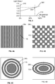
- the extraction efficiency has been found to be substantially linear with respect to the proportion of roughened surface area, as illustrated by the line 350 in FIG. 3 .
- the light output is normalized to the amount of light that the original light emitting device 110 with an un-roughened surface 115.
- a fully roughened surface 285 provides about twice the light output as an un-roughened surface 115.
- the light output is about 1.75 times the light output of the un-roughened surface 115.
- FIGs. 4A-4D illustrate example patterns of selective roughened light emitting surfaces.
- One of skill in the art will recognize that any of a variety of roughened patterns may be used to achieve different optical effects while also controlling the amount of light being emitted from the surface.
- FIG. 4A illustrates an example surface area of a device having roughened areas 285 and un-roughened areas 115 arranged in vertical bands.
- the proportion of roughened area is about 75%, which, in the example of a linear relationship 350 between light output 320 and roughened area 310 of FIG. 3 , will provide for a light output that is about 1.75 times the amount of light provided by the light emitting device before roughening.
- bands of brighter light from the roughened areas 285 will be produced, and may be objectionable.
- alternative patterns may be defined having the desired proportion of roughened area with less noticeable patterns. For example, instead of the nine bright roughened bands 285 of FIG. 4A , with clearly distinguishable dimmer un-roughened bands 115, hundreds of roughened bands 285 could be provided, with correspondingly smaller dimmer bands 115 that are indistinguishable by the human eye.
- FIG. 4B illustrates a checker-board like arrangement of roughened areas 285 and un-roughened areas 115.
- the example pattern provides for a proportion of roughened area of about 50%, which, in the example of FIG. 3 , will provide a light output of about 1.5 times the amount of light provided by the light emitting device before roughening.
- the contrast between the brighter light over the areas 285 and dimmer light over the areas 115 will be less noticeable than a pattern of bands having the same proportion of roughened areas 285.
- the number of distinct areas 285, 115 may be increased to reduce any noticeable optical anomalies.
- the roughened areas 285 are arranged to provide a light output pattern that will be brighter in the center region, and progressively dimmer as the distance from the center increases, providing a spotlight-like pattern.
- the rings 285, 115 will be sized to provide the desired amount of light output based on the proportion of these roughened 285 and un-roughened 115 areas.
- the roughened areas 285 are arranged to provide a bright-center pattern with an elliptical light output pattern.
- patterns 4A-4D are provided merely to illustrate that virtually any pattern may be used to create a desired optical effect while at the same time controlling the amount of light that will be emitted from the light emitting surface.
- Other patterns will be evident to one of skill in the art.
- the un-roughened pattern 285 at the center of the surface may be as illustrated, while the area beyond this center may be a less noticeable pattern, such as the checker-board arrangement of FIG. 4B .
- the mask may also define a graphic or decorative image.
- the invention in an embodiment wherein a greater range of control is provided by further limiting the amount of light that is emitted from the un-roughened surface 115. That is, in FIG. 3 , the relation 350 between the light output 320 and the roughened area 310 is assumed to range from totally flat surface 115 to a totally roughened surface 185. However, if regions of the un-roughened surface are opaque, the light output may be reduced below the amount of light that is produced by a (non-opaque) totally flat surface 115. Such opacity may be achieved by leaving some or all of the mask material 235 on the surface of the selectively etched device 280 of FIG. 2 .
- a forced Gaussian profile may be produced, for example, by creating a bulls-eye pattern wherein a center section is roughened completely and other sections are roughened at lower percentages.
- the variation in roughening may be produced by selectively applying multiple stages of the roughening process, by using different roughen-inhibiting materials, by growing etch-stop layers at different depths, and so on.
- a computer program may be stored/distributed on a suitable medium, such as an optical storage medium or a solid-state medium supplied together with or as part of other hardware, but may also be distributed in other forms, such as via the Internet or other wired or wireless telecommunication systems. Any reference signs in the claims should not be construed as limiting the scope.
Landscapes
- Led Devices (AREA)
- Drying Of Semiconductors (AREA)
- Led Device Packages (AREA)
- Non-Portable Lighting Devices Or Systems Thereof (AREA)
Claims (15)
- Verfahren, Folgendes umfassend:Erzeugen einer lichtemittierenden Vorrichtung (280) mit einer Oberfläche, wobei die lichtemittierende Vorrichtung dafür strukturiert ist, Licht durch eine definierte lichtemittierende Oberfläche zu emittieren,wobei die definierte lichtemittierende Oberfläche ein Abschnitt der Oberfläche der Vorrichtung ist, der in der Lage ist, das in der Vorrichtung erzeugt Licht zu emittieren, undwobei die definierte lichtemittierende Oberfläche keine Abschnitte der Oberfläche der Vorrichtung beinhaltet, die nicht in der Lage sind, das Licht zu emittieren, insbesondere die Abschnitte der Oberfläche der Vorrichtung, die durch einen Kontakt oder eine andere Struktur bedeckt sind,Identifizieren eines oder mehrerer Auswahlbereiche in der definierten lichtemittierenden Oberfläche und Umgestalten der definierten lichtemittierenden Oberfläche, um ein Muster aus aufgerauten Oberflächenbereichen (285), die den Auswahlbereichen entsprechen, und nicht aufgerauten Oberflächenbereichen (115) zu erzeugen.
- Verfahren nach Anspruch 1, wobei das Identifizieren das Aufbringen eines Maskierungsmaterials beinhaltet, das die Auswahlbereiche definiert.
- Verfahren nach Anspruch 2, wobei das Aufbringen des Maskierungsmaterials einen fotolithografischen Prozess beinhaltet.
- Verfahren nach Anspruch 1, wobei die lichtemittierende Vorrichtung (280) Licht von den aufgerauten Oberflächenbereichen (285) mit einem ersten Lichtausgabepegel und von den nicht aufgerauten Oberflächenbereichen (115) mit einem zweiten Lichtausgabepegel emittiert, der kleiner als der erste Lichtausgabepegel ist.
- Verfahren nach Anspruch 4, wobei der erste Lichtausgabepegel ungefähr das Doppelte des zweiten Lichtausgabepegels beträgt.
- Verfahren nach Anspruch 1, wobei die Auswahlbereiche gemustert sind, um einen erkennbaren optischen Effekt bereitzustellen.
- Verfahren nach Anspruch 1, wobei das Umgestalten das Aufrauen von mindestens einem der Auswahlbereiche auf einen Rauigkeitsgrad umfasst, der sich von einem Rauigkeitsgrad eines anderen der Auswahlbereiche unterscheidet.
- Lichtemittierende Vorrichtung (280), Folgendes umfassend:eine lichtemittierende Struktur mit einer Oberfläche, wobei die lichtemittierende Struktur dafür strukturiert ist, Licht durch eine definierte lichtemittierende Oberfläche zu emittieren,wobei die definierte lichtemittierende Oberfläche ein Abschnitt der Oberfläche der Vorrichtung ist, der in der Lage ist, in der Vorrichtung erzeugtes Licht zu emittieren, undwobei die definierte lichtemittierende Oberfläche keine Abschnitte der Oberfläche der Vorrichtung beinhaltet, die nicht in der Lage sind, das Licht zu emittieren, insbesondere die Abschnitte der Oberfläche der Vorrichtung, die durch einen Kontakt oder eine andere Struktur bedeckt sind,wobei die definierte lichtemittierende Oberfläche ein Muster aus ausgerauten Oberflächenbereichen (285) und nicht aufgerauten Oberflächenbereichen (115) umfasst.
- Lichtemittierende Vorrichtung nach Anspruch 9, wobei die aufgerauten Oberflächenbereiche (285) gemustert sind, um einen erkennbaren optischen Effekt bereitzustellen.
- Lichtemittierende Vorrichtung nach Anspruch 9, wobei die lichtemittierende Vorrichtung Licht von den aufgerauten Oberflächenbereichen (285) mit einem ersten Lichtausgabepegel und von den nicht aufgerauten Oberflächenbereichen (115) mit einem zweiten Lichtausgabepegel emittiert, der kleiner als der erste Lichtausgabepegel ist.
- Lichtemittierende Vorrichtung nach Anspruch 11, wobei der erste Lichtausgabepegel ungefähr das Doppelte des zweiten Lichtausgabepegels beträgt.
- Lichtemittierende Vorrichtung nach Anspruch 9, wobei die aufgerauten Oberflächenbereiche (285) mehrere Auswahlbereiche beinhalten und mindestens einer der Auswahlbereiche auf einen Rauigkeitsgrad aufgeraut ist, der sich von einem Rauigkeitsgrad eines anderen der ausgewählten Bereiche unterscheidet.
- Lichtemittierende Vorrichtung nach Anspruch 9, wobei das Muster eine schachbrettartige Anordnung aufgerauter Oberflächenbereiche (285) und nicht aufgerauter Oberflächenbereiche (115) ist.
- Lichtemittierende Vorrichtung nach Anspruch 9, wobei die aufgerauten Oberflächenbereiche (285) dafür angeordnet sind, ein Lichtausgabemuster bereitzustellen, das in einer mittleren Region der lichtemittierenden Oberfläche heller ist und mit einem größer werdenden Abstand zur mittleren Region zunehmend dunkler wird.
- Lichtemittierende Vorrichtung nach Anspruch 9, wobei die aufgerauten Oberflächenbereiche (285) dafür angeordnet sind, ein Muster mit heller Mitte und einem elliptischen Lichtausgabemuster bereitzustellen.
Applications Claiming Priority (2)
| Application Number | Priority Date | Filing Date | Title |
|---|---|---|---|
| US201261584836P | 2012-01-10 | 2012-01-10 | |
| PCT/IB2013/050055 WO2013105004A1 (en) | 2012-01-10 | 2013-01-03 | Controlled led light output by selective area roughening |
Publications (2)
| Publication Number | Publication Date |
|---|---|
| EP2803093A1 EP2803093A1 (de) | 2014-11-19 |
| EP2803093B1 true EP2803093B1 (de) | 2019-06-26 |
Family
ID=47739410
Family Applications (1)
| Application Number | Title | Priority Date | Filing Date |
|---|---|---|---|
| EP13705009.2A Active EP2803093B1 (de) | 2012-01-10 | 2013-01-03 | Gesteuerte led-lichtausgabe durch selektive bereichsaufrauung |
Country Status (7)
| Country | Link |
|---|---|
| US (2) | US10074772B2 (de) |
| EP (1) | EP2803093B1 (de) |
| JP (1) | JP6535465B2 (de) |
| KR (2) | KR20140117515A (de) |
| CN (2) | CN104040734B (de) |
| TW (2) | TWI646703B (de) |
| WO (1) | WO2013105004A1 (de) |
Families Citing this family (2)
| Publication number | Priority date | Publication date | Assignee | Title |
|---|---|---|---|---|
| DE102014201885A1 (de) * | 2014-02-03 | 2015-08-06 | Johnson Controls Automotive Electronics Gmbh | Abdeckscheibe für mindestens ein Anzeigeinstrument in einem Fahrzeug |
| KR101630799B1 (ko) * | 2014-11-12 | 2016-06-16 | 주식회사 레이토피아 | 발광 소자 및 그의 제조방법 |
Family Cites Families (44)
| Publication number | Priority date | Publication date | Assignee | Title |
|---|---|---|---|---|
| JPH0738146A (ja) * | 1993-07-20 | 1995-02-07 | Victor Co Of Japan Ltd | 半導体発光装置 |
| KR20030052060A (ko) * | 2001-12-20 | 2003-06-26 | 엘지전자 주식회사 | 발광 소자 및 그의 제조방법 |
| US7102175B2 (en) * | 2003-04-15 | 2006-09-05 | Matsushita Electric Industrial Co., Ltd. | Semiconductor light-emitting device and method for fabricating the same |
| US6847057B1 (en) | 2003-08-01 | 2005-01-25 | Lumileds Lighting U.S., Llc | Semiconductor light emitting devices |
| JP4124102B2 (ja) * | 2003-11-12 | 2008-07-23 | 松下電工株式会社 | 多重反射防止構造を備えた発光素子とその製造方法 |
| US7704763B2 (en) * | 2003-12-09 | 2010-04-27 | The Regents Of The University Of California | Highly efficient group-III nitride based light emitting diodes via fabrication of structures on an N-face surface |
| KR100649494B1 (ko) | 2004-08-17 | 2006-11-24 | 삼성전기주식회사 | 레이저를 이용하여 발광 다이오드 기판을 표면 처리하는발광 다이오드 제조 방법 및 이 방법에 의해 제조된 발광다이오드 |
| US7256483B2 (en) | 2004-10-28 | 2007-08-14 | Philips Lumileds Lighting Company, Llc | Package-integrated thin film LED |
| KR100638666B1 (ko) | 2005-01-03 | 2006-10-30 | 삼성전기주식회사 | 질화물 반도체 발광소자 |
| US20060204865A1 (en) * | 2005-03-08 | 2006-09-14 | Luminus Devices, Inc. | Patterned light-emitting devices |
| JP2006253298A (ja) | 2005-03-09 | 2006-09-21 | Toshiba Corp | 半導体発光素子及び半導体発光装置 |
| KR100691177B1 (ko) * | 2005-05-31 | 2007-03-09 | 삼성전기주식회사 | 백색 발광소자 |
| KR100640497B1 (ko) | 2005-11-24 | 2006-11-01 | 삼성전기주식회사 | 수직 구조 질화갈륨계 발광다이오드 소자 |
| JP4986445B2 (ja) * | 2005-12-13 | 2012-07-25 | 昭和電工株式会社 | 窒化ガリウム系化合物半導体発光素子 |
| JP2007220865A (ja) * | 2006-02-16 | 2007-08-30 | Sumitomo Chemical Co Ltd | 3族窒化物半導体発光素子およびその製造方法 |
| TWI288979B (en) | 2006-02-23 | 2007-10-21 | Arima Optoelectronics Corp | Light emitting diode bonded with metal diffusion and manufacturing method thereof |
| JP2007273975A (ja) * | 2006-03-10 | 2007-10-18 | Matsushita Electric Works Ltd | 発光素子 |
| CN101395728B (zh) * | 2006-03-10 | 2011-04-13 | 松下电工株式会社 | 发光元件及其制造方法 |
| CN101079460B (zh) * | 2006-05-23 | 2010-05-12 | 台达电子工业股份有限公司 | 发光装置 |
| JP2008066557A (ja) * | 2006-09-08 | 2008-03-21 | Matsushita Electric Ind Co Ltd | 半導体発光装置および半導体発光装置の製造方法 |
| KR101262226B1 (ko) | 2006-10-31 | 2013-05-15 | 삼성전자주식회사 | 반도체 발광 소자의 제조방법 |
| TW200822788A (en) | 2006-11-09 | 2008-05-16 | Univ Nat Central | Method of using laser in fabricating GaN device |
| TW200905928A (en) * | 2007-03-29 | 2009-02-01 | Univ California | Dual surface-roughened N-face high-brightness LED |
| KR20100097179A (ko) | 2007-11-30 | 2010-09-02 | 더 리전트 오브 더 유니버시티 오브 캘리포니아 | 표면을 거칠게하여 높은 광 추출 효율을 갖는 질화물계 발광 다이오드 |
| CN101226977A (zh) | 2007-12-18 | 2008-07-23 | 西安电子科技大学 | GaN基发光二极管表面粗化的处理方法 |
| RU2436195C1 (ru) | 2007-12-28 | 2011-12-10 | Нития Корпорейшн | Полупроводниковый светоизлучающий прибор и способ его изготовления |
| JP5343860B2 (ja) * | 2007-12-28 | 2013-11-13 | 三菱化学株式会社 | GaN系LED素子用電極およびGaN系LED素子ならびにそれらの製造方法。 |
| US8105853B2 (en) * | 2008-06-27 | 2012-01-31 | Bridgelux, Inc. | Surface-textured encapsulations for use with light emitting diodes |
| TWI384651B (zh) | 2008-08-20 | 2013-02-01 | Au Optronics Corp | 發光二極體結構及其製造方法 |
| JP2010056459A (ja) * | 2008-08-29 | 2010-03-11 | Kyocera Corp | 発光素子の製造方法 |
| US7749782B1 (en) * | 2008-12-17 | 2010-07-06 | Palo Alto Research Center Incorporated | Laser roughening to improve LED emissions |
| US8471288B2 (en) * | 2009-09-15 | 2013-06-25 | Toyoda Gosei Co., Ltd. | Group III nitride semiconductor light-emitting device including an auxiliary electrode in contact with a back surface of an n-type layer |
| JP5304563B2 (ja) * | 2009-09-15 | 2013-10-02 | 豊田合成株式会社 | Iii族窒化物半導体発光素子 |
| JP2011100829A (ja) | 2009-11-05 | 2011-05-19 | Toshiba Corp | 半導体発光装置の製造方法および半導体発光装置 |
| TWI412161B (zh) | 2009-11-06 | 2013-10-11 | Semileds Optoelectronics Co | 發光二極體裝置 |
| TWI411135B (zh) | 2009-12-24 | 2013-10-01 | Walsin Lihwa Corp | 發光裝置及增益發光裝置的電注入效率和出光效率的方法 |
| KR101039880B1 (ko) * | 2010-04-28 | 2011-06-09 | 엘지이노텍 주식회사 | 발광소자 및 발광소자 패키지 |
| US8154042B2 (en) | 2010-04-29 | 2012-04-10 | Koninklijke Philips Electronics N V | Light emitting device with trenches and a top contact |
| TW201145579A (en) * | 2010-06-08 | 2011-12-16 | Epileds Technologies Inc | Substrate for light-emitting diode |
| US20120023516A1 (en) * | 2010-07-21 | 2012-01-26 | Robert Wolinsky | System and method for verifying home television audience viewership via a set-top box |
| JP2011066453A (ja) | 2010-12-27 | 2011-03-31 | Toshiba Corp | 半導体発光素子及び半導体発光装置 |
| CN102169936A (zh) * | 2011-02-16 | 2011-08-31 | 亚威朗光电(中国)有限公司 | 图形衬底和led芯片 |
| JP5050109B2 (ja) * | 2011-03-14 | 2012-10-17 | 株式会社東芝 | 半導体発光素子 |
| CN104160520A (zh) * | 2012-02-01 | 2014-11-19 | 松下电器产业株式会社 | 半导体发光元件、其制造方法和光源装置 |
-
2013
- 2013-01-03 EP EP13705009.2A patent/EP2803093B1/de active Active
- 2013-01-03 WO PCT/IB2013/050055 patent/WO2013105004A1/en not_active Ceased
- 2013-01-03 CN CN201380005153.9A patent/CN104040734B/zh not_active Expired - Fee Related
- 2013-01-03 KR KR1020147022241A patent/KR20140117515A/ko not_active Ceased
- 2013-01-03 JP JP2014550792A patent/JP6535465B2/ja not_active Expired - Fee Related
- 2013-01-03 KR KR1020197031019A patent/KR102158440B1/ko not_active Expired - Fee Related
- 2013-01-03 US US14/363,354 patent/US10074772B2/en active Active
- 2013-01-03 CN CN201810745910.0A patent/CN108767076B/zh not_active Expired - Fee Related
- 2013-01-10 TW TW102100977A patent/TWI646703B/zh not_active IP Right Cessation
- 2013-01-10 TW TW106122206A patent/TWI646704B/zh not_active IP Right Cessation
-
2018
- 2018-03-28 US US15/938,826 patent/US20180219128A1/en not_active Abandoned
Non-Patent Citations (1)
| Title |
|---|
| None * |
Also Published As
| Publication number | Publication date |
|---|---|
| TWI646704B (zh) | 2019-01-01 |
| EP2803093A1 (de) | 2014-11-19 |
| CN108767076B (zh) | 2021-10-15 |
| CN108767076A (zh) | 2018-11-06 |
| US20140327030A1 (en) | 2014-11-06 |
| CN104040734B (zh) | 2018-07-20 |
| KR20190122271A (ko) | 2019-10-29 |
| KR102158440B1 (ko) | 2020-09-23 |
| WO2013105004A1 (en) | 2013-07-18 |
| US20180219128A1 (en) | 2018-08-02 |
| KR20140117515A (ko) | 2014-10-07 |
| TW201340393A (zh) | 2013-10-01 |
| TWI646703B (zh) | 2019-01-01 |
| JP2015503849A (ja) | 2015-02-02 |
| JP6535465B2 (ja) | 2019-06-26 |
| US10074772B2 (en) | 2018-09-11 |
| TW201826562A (zh) | 2018-07-16 |
| CN104040734A (zh) | 2014-09-10 |
Similar Documents
| Publication | Publication Date | Title |
|---|---|---|
| US7419912B2 (en) | Laser patterning of light emitting devices | |
| CN104638078B (zh) | 发光二极管及其制作方法 | |
| TWI538251B (zh) | 用於形成超微型發光二極體之方法 | |
| EP2856522B1 (de) | Verbesserte lichtextraktion mittels grössen- und formkontrolle während der led-oberflächenaufrauung | |
| US20170148952A1 (en) | Thin-film flip-chip light emitting diode having roughening surface and method for manufacturing the same | |
| EP2803093B1 (de) | Gesteuerte led-lichtausgabe durch selektive bereichsaufrauung | |
| JP2005116615A (ja) | 半導体発光素子及びその製造方法 | |
| EP2846365A1 (de) | Leuchtdioden und Herstellungsverfahren dafür | |
| KR100499131B1 (ko) | 고효율 광방출 다이오드 및 그 제조방법 | |
| JP2009010060A (ja) | 発光ダイオード及びその製造方法 | |
| TWI596799B (zh) | 控制發光裝置之方法 | |
| KR20210005175A (ko) | 자외선 레이저를 사용한 led 표면 개질 | |
| CN111048633A (zh) | 一种倒装led芯片的制作方法 | |
| CN117438515B (zh) | 一种led芯片粗化方法及led芯片 | |
| US12622095B2 (en) | Optical device and method for producing an optical device | |
| KR100664981B1 (ko) | III-V 족 GaN 계 화합물 반도체 발광소자의 제조방법 | |
| WO2013105015A1 (en) | Sidewall etching of led die to improve light extraction | |
| CN104377276A (zh) | 覆晶led芯片的制作方法 | |
| KR20150058603A (ko) | 발광다이오드 제조방법 및 이를 통해 제조된 발광다이오드 |
Legal Events
| Date | Code | Title | Description |
|---|---|---|---|
| PUAI | Public reference made under article 153(3) epc to a published international application that has entered the european phase |
Free format text: ORIGINAL CODE: 0009012 |
|
| 17P | Request for examination filed |
Effective date: 20140811 |
|
| AK | Designated contracting states |
Kind code of ref document: A1 Designated state(s): AL AT BE BG CH CY CZ DE DK EE ES FI FR GB GR HR HU IE IS IT LI LT LU LV MC MK MT NL NO PL PT RO RS SE SI SK SM TR |
|
| DAX | Request for extension of the european patent (deleted) | ||
| STAA | Information on the status of an ep patent application or granted ep patent |
Free format text: STATUS: EXAMINATION IS IN PROGRESS |
|
| 17Q | First examination report despatched |
Effective date: 20180130 |
|
| RAP1 | Party data changed (applicant data changed or rights of an application transferred) |
Owner name: LUMILEDS HOLDING B.V. |
|
| RAP1 | Party data changed (applicant data changed or rights of an application transferred) |
Owner name: LUMILEDS HOLDING B.V. |
|
| GRAP | Despatch of communication of intention to grant a patent |
Free format text: ORIGINAL CODE: EPIDOSNIGR1 |
|
| STAA | Information on the status of an ep patent application or granted ep patent |
Free format text: STATUS: GRANT OF PATENT IS INTENDED |
|
| INTG | Intention to grant announced |
Effective date: 20190301 |
|
| GRAS | Grant fee paid |
Free format text: ORIGINAL CODE: EPIDOSNIGR3 |
|
| GRAA | (expected) grant |
Free format text: ORIGINAL CODE: 0009210 |
|
| STAA | Information on the status of an ep patent application or granted ep patent |
Free format text: STATUS: THE PATENT HAS BEEN GRANTED |
|
| AK | Designated contracting states |
Kind code of ref document: B1 Designated state(s): AL AT BE BG CH CY CZ DE DK EE ES FI FR GB GR HR HU IE IS IT LI LT LU LV MC MK MT NL NO PL PT RO RS SE SI SK SM TR |
|
| REG | Reference to a national code |
Ref country code: GB Ref legal event code: FG4D |
|
| REG | Reference to a national code |
Ref country code: CH Ref legal event code: EP |
|
| REG | Reference to a national code |
Ref country code: DE Ref legal event code: R096 Ref document number: 602013057056 Country of ref document: DE |
|
| REG | Reference to a national code |
Ref country code: AT Ref legal event code: REF Ref document number: 1149311 Country of ref document: AT Kind code of ref document: T Effective date: 20190715 |
|
| REG | Reference to a national code |
Ref country code: IE Ref legal event code: FG4D |
|
| REG | Reference to a national code |
Ref country code: NL Ref legal event code: MP Effective date: 20190626 |
|
| PG25 | Lapsed in a contracting state [announced via postgrant information from national office to epo] |
Ref country code: FI Free format text: LAPSE BECAUSE OF FAILURE TO SUBMIT A TRANSLATION OF THE DESCRIPTION OR TO PAY THE FEE WITHIN THE PRESCRIBED TIME-LIMIT Effective date: 20190626 Ref country code: SE Free format text: LAPSE BECAUSE OF FAILURE TO SUBMIT A TRANSLATION OF THE DESCRIPTION OR TO PAY THE FEE WITHIN THE PRESCRIBED TIME-LIMIT Effective date: 20190626 Ref country code: LT Free format text: LAPSE BECAUSE OF FAILURE TO SUBMIT A TRANSLATION OF THE DESCRIPTION OR TO PAY THE FEE WITHIN THE PRESCRIBED TIME-LIMIT Effective date: 20190626 Ref country code: AL Free format text: LAPSE BECAUSE OF FAILURE TO SUBMIT A TRANSLATION OF THE DESCRIPTION OR TO PAY THE FEE WITHIN THE PRESCRIBED TIME-LIMIT Effective date: 20190626 Ref country code: HR Free format text: LAPSE BECAUSE OF FAILURE TO SUBMIT A TRANSLATION OF THE DESCRIPTION OR TO PAY THE FEE WITHIN THE PRESCRIBED TIME-LIMIT Effective date: 20190626 Ref country code: NO Free format text: LAPSE BECAUSE OF FAILURE TO SUBMIT A TRANSLATION OF THE DESCRIPTION OR TO PAY THE FEE WITHIN THE PRESCRIBED TIME-LIMIT Effective date: 20190926 |
|
| REG | Reference to a national code |
Ref country code: LT Ref legal event code: MG4D |
|
| PG25 | Lapsed in a contracting state [announced via postgrant information from national office to epo] |
Ref country code: LV Free format text: LAPSE BECAUSE OF FAILURE TO SUBMIT A TRANSLATION OF THE DESCRIPTION OR TO PAY THE FEE WITHIN THE PRESCRIBED TIME-LIMIT Effective date: 20190626 Ref country code: GR Free format text: LAPSE BECAUSE OF FAILURE TO SUBMIT A TRANSLATION OF THE DESCRIPTION OR TO PAY THE FEE WITHIN THE PRESCRIBED TIME-LIMIT Effective date: 20190927 Ref country code: RS Free format text: LAPSE BECAUSE OF FAILURE TO SUBMIT A TRANSLATION OF THE DESCRIPTION OR TO PAY THE FEE WITHIN THE PRESCRIBED TIME-LIMIT Effective date: 20190626 Ref country code: BG Free format text: LAPSE BECAUSE OF FAILURE TO SUBMIT A TRANSLATION OF THE DESCRIPTION OR TO PAY THE FEE WITHIN THE PRESCRIBED TIME-LIMIT Effective date: 20190926 |
|
| REG | Reference to a national code |
Ref country code: AT Ref legal event code: MK05 Ref document number: 1149311 Country of ref document: AT Kind code of ref document: T Effective date: 20190626 |
|
| PG25 | Lapsed in a contracting state [announced via postgrant information from national office to epo] |
Ref country code: PT Free format text: LAPSE BECAUSE OF FAILURE TO SUBMIT A TRANSLATION OF THE DESCRIPTION OR TO PAY THE FEE WITHIN THE PRESCRIBED TIME-LIMIT Effective date: 20191028 Ref country code: RO Free format text: LAPSE BECAUSE OF FAILURE TO SUBMIT A TRANSLATION OF THE DESCRIPTION OR TO PAY THE FEE WITHIN THE PRESCRIBED TIME-LIMIT Effective date: 20190626 Ref country code: NL Free format text: LAPSE BECAUSE OF FAILURE TO SUBMIT A TRANSLATION OF THE DESCRIPTION OR TO PAY THE FEE WITHIN THE PRESCRIBED TIME-LIMIT Effective date: 20190626 Ref country code: CZ Free format text: LAPSE BECAUSE OF FAILURE TO SUBMIT A TRANSLATION OF THE DESCRIPTION OR TO PAY THE FEE WITHIN THE PRESCRIBED TIME-LIMIT Effective date: 20190626 Ref country code: EE Free format text: LAPSE BECAUSE OF FAILURE TO SUBMIT A TRANSLATION OF THE DESCRIPTION OR TO PAY THE FEE WITHIN THE PRESCRIBED TIME-LIMIT Effective date: 20190626 Ref country code: AT Free format text: LAPSE BECAUSE OF FAILURE TO SUBMIT A TRANSLATION OF THE DESCRIPTION OR TO PAY THE FEE WITHIN THE PRESCRIBED TIME-LIMIT Effective date: 20190626 Ref country code: SK Free format text: LAPSE BECAUSE OF FAILURE TO SUBMIT A TRANSLATION OF THE DESCRIPTION OR TO PAY THE FEE WITHIN THE PRESCRIBED TIME-LIMIT Effective date: 20190626 |
|
| PG25 | Lapsed in a contracting state [announced via postgrant information from national office to epo] |
Ref country code: IT Free format text: LAPSE BECAUSE OF FAILURE TO SUBMIT A TRANSLATION OF THE DESCRIPTION OR TO PAY THE FEE WITHIN THE PRESCRIBED TIME-LIMIT Effective date: 20190626 Ref country code: ES Free format text: LAPSE BECAUSE OF FAILURE TO SUBMIT A TRANSLATION OF THE DESCRIPTION OR TO PAY THE FEE WITHIN THE PRESCRIBED TIME-LIMIT Effective date: 20190626 Ref country code: SM Free format text: LAPSE BECAUSE OF FAILURE TO SUBMIT A TRANSLATION OF THE DESCRIPTION OR TO PAY THE FEE WITHIN THE PRESCRIBED TIME-LIMIT Effective date: 20190626 Ref country code: IS Free format text: LAPSE BECAUSE OF FAILURE TO SUBMIT A TRANSLATION OF THE DESCRIPTION OR TO PAY THE FEE WITHIN THE PRESCRIBED TIME-LIMIT Effective date: 20191026 |
|
| PG25 | Lapsed in a contracting state [announced via postgrant information from national office to epo] |
Ref country code: TR Free format text: LAPSE BECAUSE OF FAILURE TO SUBMIT A TRANSLATION OF THE DESCRIPTION OR TO PAY THE FEE WITHIN THE PRESCRIBED TIME-LIMIT Effective date: 20190626 |
|
| PG25 | Lapsed in a contracting state [announced via postgrant information from national office to epo] |
Ref country code: DK Free format text: LAPSE BECAUSE OF FAILURE TO SUBMIT A TRANSLATION OF THE DESCRIPTION OR TO PAY THE FEE WITHIN THE PRESCRIBED TIME-LIMIT Effective date: 20190626 Ref country code: PL Free format text: LAPSE BECAUSE OF FAILURE TO SUBMIT A TRANSLATION OF THE DESCRIPTION OR TO PAY THE FEE WITHIN THE PRESCRIBED TIME-LIMIT Effective date: 20190626 |
|
| PG25 | Lapsed in a contracting state [announced via postgrant information from national office to epo] |
Ref country code: IS Free format text: LAPSE BECAUSE OF FAILURE TO SUBMIT A TRANSLATION OF THE DESCRIPTION OR TO PAY THE FEE WITHIN THE PRESCRIBED TIME-LIMIT Effective date: 20200224 |
|
| REG | Reference to a national code |
Ref country code: DE Ref legal event code: R097 Ref document number: 602013057056 Country of ref document: DE |
|
| PLBE | No opposition filed within time limit |
Free format text: ORIGINAL CODE: 0009261 |
|
| STAA | Information on the status of an ep patent application or granted ep patent |
Free format text: STATUS: NO OPPOSITION FILED WITHIN TIME LIMIT |
|
| PG2D | Information on lapse in contracting state deleted |
Ref country code: IS |
|
| 26N | No opposition filed |
Effective date: 20200603 |
|
| PG25 | Lapsed in a contracting state [announced via postgrant information from national office to epo] |
Ref country code: MC Free format text: LAPSE BECAUSE OF FAILURE TO SUBMIT A TRANSLATION OF THE DESCRIPTION OR TO PAY THE FEE WITHIN THE PRESCRIBED TIME-LIMIT Effective date: 20190626 Ref country code: SI Free format text: LAPSE BECAUSE OF FAILURE TO SUBMIT A TRANSLATION OF THE DESCRIPTION OR TO PAY THE FEE WITHIN THE PRESCRIBED TIME-LIMIT Effective date: 20190626 |
|
| REG | Reference to a national code |
Ref country code: CH Ref legal event code: PL |
|
| REG | Reference to a national code |
Ref country code: BE Ref legal event code: MM Effective date: 20200131 |
|
| PG25 | Lapsed in a contracting state [announced via postgrant information from national office to epo] |
Ref country code: LU Free format text: LAPSE BECAUSE OF NON-PAYMENT OF DUE FEES Effective date: 20200103 |
|
| PG25 | Lapsed in a contracting state [announced via postgrant information from national office to epo] |
Ref country code: LI Free format text: LAPSE BECAUSE OF NON-PAYMENT OF DUE FEES Effective date: 20200131 Ref country code: CH Free format text: LAPSE BECAUSE OF NON-PAYMENT OF DUE FEES Effective date: 20200131 Ref country code: BE Free format text: LAPSE BECAUSE OF NON-PAYMENT OF DUE FEES Effective date: 20200131 |
|
| PG25 | Lapsed in a contracting state [announced via postgrant information from national office to epo] |
Ref country code: IE Free format text: LAPSE BECAUSE OF NON-PAYMENT OF DUE FEES Effective date: 20200103 |
|
| PG25 | Lapsed in a contracting state [announced via postgrant information from national office to epo] |
Ref country code: MT Free format text: LAPSE BECAUSE OF FAILURE TO SUBMIT A TRANSLATION OF THE DESCRIPTION OR TO PAY THE FEE WITHIN THE PRESCRIBED TIME-LIMIT Effective date: 20190626 Ref country code: CY Free format text: LAPSE BECAUSE OF FAILURE TO SUBMIT A TRANSLATION OF THE DESCRIPTION OR TO PAY THE FEE WITHIN THE PRESCRIBED TIME-LIMIT Effective date: 20190626 |
|
| PG25 | Lapsed in a contracting state [announced via postgrant information from national office to epo] |
Ref country code: MK Free format text: LAPSE BECAUSE OF FAILURE TO SUBMIT A TRANSLATION OF THE DESCRIPTION OR TO PAY THE FEE WITHIN THE PRESCRIBED TIME-LIMIT Effective date: 20190626 |
|
| PGFP | Annual fee paid to national office [announced via postgrant information from national office to epo] |
Ref country code: FR Payment date: 20230124 Year of fee payment: 11 |
|
| PGFP | Annual fee paid to national office [announced via postgrant information from national office to epo] |
Ref country code: GB Payment date: 20230124 Year of fee payment: 11 Ref country code: DE Payment date: 20230127 Year of fee payment: 11 |
|
| P01 | Opt-out of the competence of the unified patent court (upc) registered |
Effective date: 20230530 |
|
| REG | Reference to a national code |
Ref country code: DE Ref legal event code: R119 Ref document number: 602013057056 Country of ref document: DE |
|
| GBPC | Gb: european patent ceased through non-payment of renewal fee |
Effective date: 20240103 |
|
| PG25 | Lapsed in a contracting state [announced via postgrant information from national office to epo] |
Ref country code: DE Free format text: LAPSE BECAUSE OF NON-PAYMENT OF DUE FEES Effective date: 20240801 |
|
| PG25 | Lapsed in a contracting state [announced via postgrant information from national office to epo] |
Ref country code: GB Free format text: LAPSE BECAUSE OF NON-PAYMENT OF DUE FEES Effective date: 20240103 |
|
| PG25 | Lapsed in a contracting state [announced via postgrant information from national office to epo] |
Ref country code: FR Free format text: LAPSE BECAUSE OF NON-PAYMENT OF DUE FEES Effective date: 20240131 |
|
| PG25 | Lapsed in a contracting state [announced via postgrant information from national office to epo] |
Ref country code: GB Free format text: LAPSE BECAUSE OF NON-PAYMENT OF DUE FEES Effective date: 20240103 Ref country code: FR Free format text: LAPSE BECAUSE OF NON-PAYMENT OF DUE FEES Effective date: 20240131 Ref country code: DE Free format text: LAPSE BECAUSE OF NON-PAYMENT OF DUE FEES Effective date: 20240801 |