EP2259285B1 - High efficiency multi-color electro-phosphorescent OLEDs. - Google Patents
High efficiency multi-color electro-phosphorescent OLEDs. Download PDFInfo
- Publication number
- EP2259285B1 EP2259285B1 EP10181013.3A EP10181013A EP2259285B1 EP 2259285 B1 EP2259285 B1 EP 2259285B1 EP 10181013 A EP10181013 A EP 10181013A EP 2259285 B1 EP2259285 B1 EP 2259285B1
- Authority
- EP
- European Patent Office
- Prior art keywords
- layer
- emissive
- emission
- doped
- phosphorescent
- Prior art date
- Legal status (The legal status is an assumption and is not a legal conclusion. Google has not performed a legal analysis and makes no representation as to the accuracy of the status listed.)
- Expired - Lifetime
Links
- 239000000463 material Substances 0.000 claims abstract description 102
- 239000002019 doping agent Substances 0.000 claims abstract description 69
- 230000000903 blocking effect Effects 0.000 claims description 24
- 238000002347 injection Methods 0.000 claims description 6
- 239000007924 injection Substances 0.000 claims description 6
- 150000002902 organometallic compounds Chemical class 0.000 claims description 3
- 239000010410 layer Substances 0.000 description 186
- VFUDMQLBKNMONU-UHFFFAOYSA-N 9-[4-(4-carbazol-9-ylphenyl)phenyl]carbazole Chemical group C12=CC=CC=C2C2=CC=CC=C2N1C1=CC=C(C=2C=CC(=CC=2)N2C3=CC=CC=C3C3=CC=CC=C32)C=C1 VFUDMQLBKNMONU-UHFFFAOYSA-N 0.000 description 48
- UEEXRMUCXBPYOV-UHFFFAOYSA-N iridium;2-phenylpyridine Chemical compound [Ir].C1=CC=CC=C1C1=CC=CC=N1.C1=CC=CC=C1C1=CC=CC=N1.C1=CC=CC=C1C1=CC=CC=N1 UEEXRMUCXBPYOV-UHFFFAOYSA-N 0.000 description 36
- CUJRVFIICFDLGR-UHFFFAOYSA-N acetylacetonate Chemical compound CC(=O)[CH-]C(C)=O CUJRVFIICFDLGR-UHFFFAOYSA-N 0.000 description 31
- 238000012546 transfer Methods 0.000 description 31
- 238000000034 method Methods 0.000 description 23
- 238000009792 diffusion process Methods 0.000 description 19
- 230000015572 biosynthetic process Effects 0.000 description 17
- 239000000758 substrate Substances 0.000 description 17
- 238000000151 deposition Methods 0.000 description 14
- PQXKHYXIUOZZFA-UHFFFAOYSA-M lithium fluoride Chemical compound [Li+].[F-] PQXKHYXIUOZZFA-UHFFFAOYSA-M 0.000 description 14
- OAICVXFJPJFONN-UHFFFAOYSA-N Phosphorus Chemical compound [P] OAICVXFJPJFONN-UHFFFAOYSA-N 0.000 description 13
- -1 benzthiazole compound Chemical class 0.000 description 13
- IBHBKWKFFTZAHE-UHFFFAOYSA-N n-[4-[4-(n-naphthalen-1-ylanilino)phenyl]phenyl]-n-phenylnaphthalen-1-amine Chemical compound C1=CC=CC=C1N(C=1C2=CC=CC=C2C=CC=1)C1=CC=C(C=2C=CC(=CC=2)N(C=2C=CC=CC=2)C=2C3=CC=CC=C3C=CC=2)C=C1 IBHBKWKFFTZAHE-UHFFFAOYSA-N 0.000 description 13
- 230000006870 function Effects 0.000 description 12
- 235000019557 luminance Nutrition 0.000 description 12
- 229910052751 metal Inorganic materials 0.000 description 11
- 239000002184 metal Substances 0.000 description 11
- 239000012044 organic layer Substances 0.000 description 11
- 230000008569 process Effects 0.000 description 11
- 230000005281 excited state Effects 0.000 description 10
- 230000008021 deposition Effects 0.000 description 9
- 230000037230 mobility Effects 0.000 description 9
- 229920000642 polymer Polymers 0.000 description 9
- 229920000144 PEDOT:PSS Polymers 0.000 description 8
- 230000005540 biological transmission Effects 0.000 description 8
- 230000006798 recombination Effects 0.000 description 8
- 238000005215 recombination Methods 0.000 description 8
- 238000001228 spectrum Methods 0.000 description 7
- 238000004519 manufacturing process Methods 0.000 description 6
- 230000003287 optical effect Effects 0.000 description 6
- POILWHVDKZOXJZ-ARJAWSKDSA-M (z)-4-oxopent-2-en-2-olate Chemical compound C\C([O-])=C\C(C)=O POILWHVDKZOXJZ-ARJAWSKDSA-M 0.000 description 5
- STTGYIUESPWXOW-UHFFFAOYSA-N 2,9-dimethyl-4,7-diphenyl-1,10-phenanthroline Chemical compound C=12C=CC3=C(C=4C=CC=CC=4)C=C(C)N=C3C2=NC(C)=CC=1C1=CC=CC=C1 STTGYIUESPWXOW-UHFFFAOYSA-N 0.000 description 5
- 230000008901 benefit Effects 0.000 description 5
- 239000011521 glass Substances 0.000 description 5
- 238000005286 illumination Methods 0.000 description 5
- 229910052741 iridium Inorganic materials 0.000 description 5
- 238000004020 luminiscence type Methods 0.000 description 5
- IJGRMHOSHXDMSA-UHFFFAOYSA-N Atomic nitrogen Chemical compound N#N IJGRMHOSHXDMSA-UHFFFAOYSA-N 0.000 description 4
- 230000007423 decrease Effects 0.000 description 4
- 238000013461 design Methods 0.000 description 4
- ZUOUZKKEUPVFJK-UHFFFAOYSA-N diphenyl Chemical compound C1=CC=CC=C1C1=CC=CC=C1 ZUOUZKKEUPVFJK-UHFFFAOYSA-N 0.000 description 4
- 238000001194 electroluminescence spectrum Methods 0.000 description 4
- AMGQUBHHOARCQH-UHFFFAOYSA-N indium;oxotin Chemical compound [In].[Sn]=O AMGQUBHHOARCQH-UHFFFAOYSA-N 0.000 description 4
- GKOZUEZYRPOHIO-UHFFFAOYSA-N iridium atom Chemical compound [Ir] GKOZUEZYRPOHIO-UHFFFAOYSA-N 0.000 description 4
- 229910052757 nitrogen Inorganic materials 0.000 description 4
- 239000000523 sample Substances 0.000 description 4
- 239000002904 solvent Substances 0.000 description 4
- TVIVIEFSHFOWTE-UHFFFAOYSA-K tri(quinolin-8-yloxy)alumane Chemical compound [Al+3].C1=CN=C2C([O-])=CC=CC2=C1.C1=CN=C2C([O-])=CC=CC2=C1.C1=CN=C2C([O-])=CC=CC2=C1 TVIVIEFSHFOWTE-UHFFFAOYSA-K 0.000 description 4
- DIVZFUBWFAOMCW-UHFFFAOYSA-N 4-n-(3-methylphenyl)-1-n,1-n-bis[4-(n-(3-methylphenyl)anilino)phenyl]-4-n-phenylbenzene-1,4-diamine Chemical compound CC1=CC=CC(N(C=2C=CC=CC=2)C=2C=CC(=CC=2)N(C=2C=CC(=CC=2)N(C=2C=CC=CC=2)C=2C=C(C)C=CC=2)C=2C=CC(=CC=2)N(C=2C=CC=CC=2)C=2C=C(C)C=CC=2)=C1 DIVZFUBWFAOMCW-UHFFFAOYSA-N 0.000 description 3
- 230000007547 defect Effects 0.000 description 3
- 230000008020 evaporation Effects 0.000 description 3
- 238000001704 evaporation Methods 0.000 description 3
- 229910052737 gold Inorganic materials 0.000 description 3
- 239000010931 gold Substances 0.000 description 3
- 238000004770 highest occupied molecular orbital Methods 0.000 description 3
- 230000005525 hole transport Effects 0.000 description 3
- MILUBEOXRNEUHS-UHFFFAOYSA-N iridium(3+) Chemical compound [Ir+3] MILUBEOXRNEUHS-UHFFFAOYSA-N 0.000 description 3
- 239000011159 matrix material Substances 0.000 description 3
- SIOXPEMLGUPBBT-UHFFFAOYSA-M picolinate Chemical compound [O-]C(=O)C1=CC=CC=N1 SIOXPEMLGUPBBT-UHFFFAOYSA-M 0.000 description 3
- BASFCYQUMIYNBI-UHFFFAOYSA-N platinum Chemical compound [Pt] BASFCYQUMIYNBI-UHFFFAOYSA-N 0.000 description 3
- 238000002207 thermal evaporation Methods 0.000 description 3
- 125000001544 thienyl group Chemical group 0.000 description 3
- OGGKVJMNFFSDEV-UHFFFAOYSA-N 3-methyl-n-[4-[4-(n-(3-methylphenyl)anilino)phenyl]phenyl]-n-phenylaniline Chemical compound CC1=CC=CC(N(C=2C=CC=CC=2)C=2C=CC(=CC=2)C=2C=CC(=CC=2)N(C=2C=CC=CC=2)C=2C=C(C)C=CC=2)=C1 OGGKVJMNFFSDEV-UHFFFAOYSA-N 0.000 description 2
- HCHKCACWOHOZIP-UHFFFAOYSA-N Zinc Chemical compound [Zn] HCHKCACWOHOZIP-UHFFFAOYSA-N 0.000 description 2
- 229910052782 aluminium Inorganic materials 0.000 description 2
- XAGFODPZIPBFFR-UHFFFAOYSA-N aluminium Chemical compound [Al] XAGFODPZIPBFFR-UHFFFAOYSA-N 0.000 description 2
- 239000010405 anode material Substances 0.000 description 2
- QVGXLLKOCUKJST-UHFFFAOYSA-N atomic oxygen Chemical compound [O] QVGXLLKOCUKJST-UHFFFAOYSA-N 0.000 description 2
- 235000010290 biphenyl Nutrition 0.000 description 2
- 239000004305 biphenyl Substances 0.000 description 2
- 239000003086 colorant Substances 0.000 description 2
- 230000003247 decreasing effect Effects 0.000 description 2
- 238000010586 diagram Methods 0.000 description 2
- 238000005566 electron beam evaporation Methods 0.000 description 2
- 238000000295 emission spectrum Methods 0.000 description 2
- 238000005516 engineering process Methods 0.000 description 2
- 239000007850 fluorescent dye Substances 0.000 description 2
- 238000003780 insertion Methods 0.000 description 2
- 230000037431 insertion Effects 0.000 description 2
- 239000004973 liquid crystal related substance Substances 0.000 description 2
- 229910052749 magnesium Inorganic materials 0.000 description 2
- 239000011777 magnesium Substances 0.000 description 2
- BLFVVZKSHYCRDR-UHFFFAOYSA-N n-[4-[4-(n-naphthalen-2-ylanilino)phenyl]phenyl]-n-phenylnaphthalen-2-amine Chemical group C1=CC=CC=C1N(C=1C=C2C=CC=CC2=CC=1)C1=CC=C(C=2C=CC(=CC=2)N(C=2C=CC=CC=2)C=2C=C3C=CC=CC3=CC=2)C=C1 BLFVVZKSHYCRDR-UHFFFAOYSA-N 0.000 description 2
- 239000012299 nitrogen atmosphere Substances 0.000 description 2
- 125000002524 organometallic group Chemical group 0.000 description 2
- 229910052760 oxygen Inorganic materials 0.000 description 2
- 239000001301 oxygen Substances 0.000 description 2
- 229920003023 plastic Polymers 0.000 description 2
- 239000004033 plastic Substances 0.000 description 2
- 125000002924 primary amino group Chemical group [H]N([H])* 0.000 description 2
- 230000001737 promoting effect Effects 0.000 description 2
- 238000009877 rendering Methods 0.000 description 2
- 150000003384 small molecules Chemical class 0.000 description 2
- 238000001947 vapour-phase growth Methods 0.000 description 2
- 238000001429 visible spectrum Methods 0.000 description 2
- 229910052725 zinc Inorganic materials 0.000 description 2
- 239000011701 zinc Substances 0.000 description 2
- 150000000183 1,3-benzoxazoles Chemical class 0.000 description 1
- GKWLILHTTGWKLQ-UHFFFAOYSA-N 2,3-dihydrothieno[3,4-b][1,4]dioxine Chemical compound O1CCOC2=CSC=C21 GKWLILHTTGWKLQ-UHFFFAOYSA-N 0.000 description 1
- ATKYPLNPUMJYCQ-UHFFFAOYSA-N 2-(2-hydroxyphenyl)-3H-1,3-benzothiazole-2-carboxylic acid Chemical compound N1C2=CC=CC=C2SC1(C(=O)O)C1=CC=CC=C1O ATKYPLNPUMJYCQ-UHFFFAOYSA-N 0.000 description 1
- IGFDHFHBTKRPJC-UHFFFAOYSA-N 2-(2-hydroxyphenyl)-3H-1,3-benzoxazole-2-carboxylic acid Chemical compound N1C2=CC=CC=C2OC1(C(=O)O)C1=CC=CC=C1O IGFDHFHBTKRPJC-UHFFFAOYSA-N 0.000 description 1
- FQJQNLKWTRGIEB-UHFFFAOYSA-N 2-(4-tert-butylphenyl)-5-[3-[5-(4-tert-butylphenyl)-1,3,4-oxadiazol-2-yl]phenyl]-1,3,4-oxadiazole Chemical compound C1=CC(C(C)(C)C)=CC=C1C1=NN=C(C=2C=C(C=CC=2)C=2OC(=NN=2)C=2C=CC(=CC=2)C(C)(C)C)O1 FQJQNLKWTRGIEB-UHFFFAOYSA-N 0.000 description 1
- DRGMQKFBFLKDOX-UHFFFAOYSA-N 2-methyl-4-[3-methyl-4-(4-methyl-n-(4-methylphenyl)anilino)phenyl]-n,n-bis(4-methylphenyl)aniline Chemical compound C1=CC(C)=CC=C1N(C=1C(=CC(=CC=1)C=1C=C(C)C(N(C=2C=CC(C)=CC=2)C=2C=CC(C)=CC=2)=CC=1)C)C1=CC=C(C)C=C1 DRGMQKFBFLKDOX-UHFFFAOYSA-N 0.000 description 1
- DGAQECJNVWCQMB-PUAWFVPOSA-M Ilexoside XXIX Chemical compound C[C@@H]1CC[C@@]2(CC[C@@]3(C(=CC[C@H]4[C@]3(CC[C@@H]5[C@@]4(CC[C@@H](C5(C)C)OS(=O)(=O)[O-])C)C)[C@@H]2[C@]1(C)O)C)C(=O)O[C@H]6[C@@H]([C@H]([C@@H]([C@H](O6)CO)O)O)O.[Na+] DGAQECJNVWCQMB-PUAWFVPOSA-M 0.000 description 1
- FYYHWMGAXLPEAU-UHFFFAOYSA-N Magnesium Chemical compound [Mg] FYYHWMGAXLPEAU-UHFFFAOYSA-N 0.000 description 1
- 229920001609 Poly(3,4-ethylenedioxythiophene) Polymers 0.000 description 1
- 241001085205 Prenanthella exigua Species 0.000 description 1
- GQKHTSORWJMTES-UHFFFAOYSA-N S1C(=CC2=C1C=CC=C2)C2=NC=CC=C2.S2C(=CC1=C2C=CC=C1)C1=NC=CC=C1.[Ir+3] Chemical compound S1C(=CC2=C1C=CC=C2)C2=NC=CC=C2.S2C(=CC1=C2C=CC=C1)C1=NC=CC=C1.[Ir+3] GQKHTSORWJMTES-UHFFFAOYSA-N 0.000 description 1
- BQCADISMDOOEFD-UHFFFAOYSA-N Silver Chemical compound [Ag] BQCADISMDOOEFD-UHFFFAOYSA-N 0.000 description 1
- 239000007983 Tris buffer Substances 0.000 description 1
- 238000000862 absorption spectrum Methods 0.000 description 1
- XEPMXWGXLQIFJN-UHFFFAOYSA-K aluminum;2-carboxyquinolin-8-olate Chemical compound [Al+3].C1=C(C([O-])=O)N=C2C(O)=CC=CC2=C1.C1=C(C([O-])=O)N=C2C(O)=CC=CC2=C1.C1=C(C([O-])=O)N=C2C(O)=CC=CC2=C1 XEPMXWGXLQIFJN-UHFFFAOYSA-K 0.000 description 1
- 239000012298 atmosphere Substances 0.000 description 1
- 230000004888 barrier function Effects 0.000 description 1
- 125000000319 biphenyl-4-yl group Chemical group [H]C1=C([H])C([H])=C([H])C([H])=C1C1=C([H])C([H])=C([*])C([H])=C1[H] 0.000 description 1
- 239000010406 cathode material Substances 0.000 description 1
- 239000002800 charge carrier Substances 0.000 description 1
- 229910052804 chromium Inorganic materials 0.000 description 1
- 239000011248 coating agent Substances 0.000 description 1
- 238000000576 coating method Methods 0.000 description 1
- 238000004891 communication Methods 0.000 description 1
- 150000001875 compounds Chemical class 0.000 description 1
- 239000004020 conductor Substances 0.000 description 1
- IOJUPLGTWVMSFF-UHFFFAOYSA-N cyclobenzothiazole Natural products C1=CC=C2SC=NC2=C1 IOJUPLGTWVMSFF-UHFFFAOYSA-N 0.000 description 1
- 230000001419 dependent effect Effects 0.000 description 1
- 239000000975 dye Substances 0.000 description 1
- 230000000694 effects Effects 0.000 description 1
- 238000001017 electron-beam sputter deposition Methods 0.000 description 1
- 239000010408 film Substances 0.000 description 1
- 229920002457 flexible plastic Polymers 0.000 description 1
- 239000011888 foil Substances 0.000 description 1
- 230000009477 glass transition Effects 0.000 description 1
- PCHJSUWPFVWCPO-UHFFFAOYSA-N gold Chemical compound [Au] PCHJSUWPFVWCPO-UHFFFAOYSA-N 0.000 description 1
- RBTKNAXYKSUFRK-UHFFFAOYSA-N heliogen blue Chemical compound [Cu].[N-]1C2=C(C=CC=C3)C3=C1N=C([N-]1)C3=CC=CC=C3C1=NC([N-]1)=C(C=CC=C3)C3=C1N=C([N-]1)C3=CC=CC=C3C1=N2 RBTKNAXYKSUFRK-UHFFFAOYSA-N 0.000 description 1
- 238000010348 incorporation Methods 0.000 description 1
- 229910052738 indium Inorganic materials 0.000 description 1
- APFVFJFRJDLVQX-UHFFFAOYSA-N indium atom Chemical compound [In] APFVFJFRJDLVQX-UHFFFAOYSA-N 0.000 description 1
- 239000003446 ligand Substances 0.000 description 1
- QSHDDOUJBYECFT-UHFFFAOYSA-N mercury Chemical compound [Hg] QSHDDOUJBYECFT-UHFFFAOYSA-N 0.000 description 1
- 229910052753 mercury Inorganic materials 0.000 description 1
- 229910001092 metal group alloy Inorganic materials 0.000 description 1
- 238000001465 metallisation Methods 0.000 description 1
- 150000002739 metals Chemical class 0.000 description 1
- 238000012986 modification Methods 0.000 description 1
- 230000004048 modification Effects 0.000 description 1
- 239000011368 organic material Substances 0.000 description 1
- 150000004866 oxadiazoles Chemical class 0.000 description 1
- KYKLWYKWCAYAJY-UHFFFAOYSA-N oxotin;zinc Chemical compound [Zn].[Sn]=O KYKLWYKWCAYAJY-UHFFFAOYSA-N 0.000 description 1
- 230000008447 perception Effects 0.000 description 1
- 150000005041 phenanthrolines Chemical class 0.000 description 1
- IEQIEDJGQAUEQZ-UHFFFAOYSA-N phthalocyanine Chemical class N1C(N=C2C3=CC=CC=C3C(N=C3C4=CC=CC=C4C(=N4)N3)=N2)=C(C=CC=C2)C2=C1N=C1C2=CC=CC=C2C4=N1 IEQIEDJGQAUEQZ-UHFFFAOYSA-N 0.000 description 1
- 229910052697 platinum Inorganic materials 0.000 description 1
- 150000003057 platinum Chemical class 0.000 description 1
- 229920002098 polyfluorene Polymers 0.000 description 1
- 229920002959 polymer blend Polymers 0.000 description 1
- 239000010453 quartz Substances 0.000 description 1
- 238000010791 quenching Methods 0.000 description 1
- 230000000171 quenching effect Effects 0.000 description 1
- 230000009467 reduction Effects 0.000 description 1
- 238000002165 resonance energy transfer Methods 0.000 description 1
- 230000004044 response Effects 0.000 description 1
- 238000012552 review Methods 0.000 description 1
- 229910052594 sapphire Inorganic materials 0.000 description 1
- 239000010980 sapphire Substances 0.000 description 1
- 229910052710 silicon Inorganic materials 0.000 description 1
- 239000010703 silicon Substances 0.000 description 1
- VYPSYNLAJGMNEJ-UHFFFAOYSA-N silicon dioxide Inorganic materials O=[Si]=O VYPSYNLAJGMNEJ-UHFFFAOYSA-N 0.000 description 1
- 229910052709 silver Inorganic materials 0.000 description 1
- 239000004332 silver Substances 0.000 description 1
- 229910052708 sodium Inorganic materials 0.000 description 1
- 239000011734 sodium Substances 0.000 description 1
- 238000004528 spin coating Methods 0.000 description 1
- 239000000126 substance Substances 0.000 description 1
- 239000010409 thin film Substances 0.000 description 1
- 125000005259 triarylamine group Chemical group 0.000 description 1
- 150000003852 triazoles Chemical class 0.000 description 1
- ODHXBMXNKOYIBV-UHFFFAOYSA-N triphenylamine Chemical compound C1=CC=CC=C1N(C=1C=CC=CC=1)C1=CC=CC=C1 ODHXBMXNKOYIBV-UHFFFAOYSA-N 0.000 description 1
- 238000007740 vapor deposition Methods 0.000 description 1
- XLYOFNOQVPJJNP-UHFFFAOYSA-N water Substances O XLYOFNOQVPJJNP-UHFFFAOYSA-N 0.000 description 1
- 238000009736 wetting Methods 0.000 description 1
Images


Classifications
-
- H—ELECTRICITY
- H05—ELECTRIC TECHNIQUES NOT OTHERWISE PROVIDED FOR
- H05B—ELECTRIC HEATING; ELECTRIC LIGHT SOURCES NOT OTHERWISE PROVIDED FOR; CIRCUIT ARRANGEMENTS FOR ELECTRIC LIGHT SOURCES, IN GENERAL
- H05B33/00—Electroluminescent light sources
- H05B33/12—Light sources with substantially two-dimensional radiating surfaces
- H05B33/18—Light sources with substantially two-dimensional radiating surfaces characterised by the nature or concentration of the activator
-
- C—CHEMISTRY; METALLURGY
- C09—DYES; PAINTS; POLISHES; NATURAL RESINS; ADHESIVES; COMPOSITIONS NOT OTHERWISE PROVIDED FOR; APPLICATIONS OF MATERIALS NOT OTHERWISE PROVIDED FOR
- C09K—MATERIALS FOR MISCELLANEOUS APPLICATIONS, NOT PROVIDED FOR ELSEWHERE
- C09K11/00—Luminescent, e.g. electroluminescent, chemiluminescent materials
- C09K11/06—Luminescent, e.g. electroluminescent, chemiluminescent materials containing organic luminescent materials
-
- H—ELECTRICITY
- H10—SEMICONDUCTOR DEVICES; ELECTRIC SOLID-STATE DEVICES NOT OTHERWISE PROVIDED FOR
- H10K—ORGANIC ELECTRIC SOLID-STATE DEVICES
- H10K50/00—Organic light-emitting devices
- H10K50/10—OLEDs or polymer light-emitting diodes [PLED]
- H10K50/11—OLEDs or polymer light-emitting diodes [PLED] characterised by the electroluminescent [EL] layers
- H10K50/125—OLEDs or polymer light-emitting diodes [PLED] characterised by the electroluminescent [EL] layers specially adapted for multicolour light emission, e.g. for emitting white light
-
- C—CHEMISTRY; METALLURGY
- C09—DYES; PAINTS; POLISHES; NATURAL RESINS; ADHESIVES; COMPOSITIONS NOT OTHERWISE PROVIDED FOR; APPLICATIONS OF MATERIALS NOT OTHERWISE PROVIDED FOR
- C09K—MATERIALS FOR MISCELLANEOUS APPLICATIONS, NOT PROVIDED FOR ELSEWHERE
- C09K2211/00—Chemical nature of organic luminescent or tenebrescent compounds
- C09K2211/10—Non-macromolecular compounds
- C09K2211/1018—Heterocyclic compounds
- C09K2211/1025—Heterocyclic compounds characterised by ligands
- C09K2211/1029—Heterocyclic compounds characterised by ligands containing one nitrogen atom as the heteroatom
-
- C—CHEMISTRY; METALLURGY
- C09—DYES; PAINTS; POLISHES; NATURAL RESINS; ADHESIVES; COMPOSITIONS NOT OTHERWISE PROVIDED FOR; APPLICATIONS OF MATERIALS NOT OTHERWISE PROVIDED FOR
- C09K—MATERIALS FOR MISCELLANEOUS APPLICATIONS, NOT PROVIDED FOR ELSEWHERE
- C09K2211/00—Chemical nature of organic luminescent or tenebrescent compounds
- C09K2211/10—Non-macromolecular compounds
- C09K2211/1018—Heterocyclic compounds
- C09K2211/1025—Heterocyclic compounds characterised by ligands
- C09K2211/1092—Heterocyclic compounds characterised by ligands containing sulfur as the only heteroatom
-
- C—CHEMISTRY; METALLURGY
- C09—DYES; PAINTS; POLISHES; NATURAL RESINS; ADHESIVES; COMPOSITIONS NOT OTHERWISE PROVIDED FOR; APPLICATIONS OF MATERIALS NOT OTHERWISE PROVIDED FOR
- C09K—MATERIALS FOR MISCELLANEOUS APPLICATIONS, NOT PROVIDED FOR ELSEWHERE
- C09K2211/00—Chemical nature of organic luminescent or tenebrescent compounds
- C09K2211/18—Metal complexes
- C09K2211/185—Metal complexes of the platinum group, i.e. Os, Ir, Pt, Ru, Rh or Pd
-
- H—ELECTRICITY
- H10—SEMICONDUCTOR DEVICES; ELECTRIC SOLID-STATE DEVICES NOT OTHERWISE PROVIDED FOR
- H10K—ORGANIC ELECTRIC SOLID-STATE DEVICES
- H10K2101/00—Properties of the organic materials covered by group H10K85/00
- H10K2101/10—Triplet emission
-
- H—ELECTRICITY
- H10—SEMICONDUCTOR DEVICES; ELECTRIC SOLID-STATE DEVICES NOT OTHERWISE PROVIDED FOR
- H10K—ORGANIC ELECTRIC SOLID-STATE DEVICES
- H10K50/00—Organic light-emitting devices
- H10K50/10—OLEDs or polymer light-emitting diodes [PLED]
- H10K50/14—Carrier transporting layers
- H10K50/15—Hole transporting layers
- H10K50/157—Hole transporting layers between the light-emitting layer and the cathode
-
- H—ELECTRICITY
- H10—SEMICONDUCTOR DEVICES; ELECTRIC SOLID-STATE DEVICES NOT OTHERWISE PROVIDED FOR
- H10K—ORGANIC ELECTRIC SOLID-STATE DEVICES
- H10K50/00—Organic light-emitting devices
- H10K50/10—OLEDs or polymer light-emitting diodes [PLED]
- H10K50/17—Carrier injection layers
-
- H—ELECTRICITY
- H10—SEMICONDUCTOR DEVICES; ELECTRIC SOLID-STATE DEVICES NOT OTHERWISE PROVIDED FOR
- H10K—ORGANIC ELECTRIC SOLID-STATE DEVICES
- H10K50/00—Organic light-emitting devices
- H10K50/10—OLEDs or polymer light-emitting diodes [PLED]
- H10K50/18—Carrier blocking layers
-
- Y—GENERAL TAGGING OF NEW TECHNOLOGICAL DEVELOPMENTS; GENERAL TAGGING OF CROSS-SECTIONAL TECHNOLOGIES SPANNING OVER SEVERAL SECTIONS OF THE IPC; TECHNICAL SUBJECTS COVERED BY FORMER USPC CROSS-REFERENCE ART COLLECTIONS [XRACs] AND DIGESTS
- Y10—TECHNICAL SUBJECTS COVERED BY FORMER USPC
- Y10S—TECHNICAL SUBJECTS COVERED BY FORMER USPC CROSS-REFERENCE ART COLLECTIONS [XRACs] AND DIGESTS
- Y10S428/00—Stock material or miscellaneous articles
- Y10S428/917—Electroluminescent
-
- Y—GENERAL TAGGING OF NEW TECHNOLOGICAL DEVELOPMENTS; GENERAL TAGGING OF CROSS-SECTIONAL TECHNOLOGIES SPANNING OVER SEVERAL SECTIONS OF THE IPC; TECHNICAL SUBJECTS COVERED BY FORMER USPC CROSS-REFERENCE ART COLLECTIONS [XRACs] AND DIGESTS
- Y10—TECHNICAL SUBJECTS COVERED BY FORMER USPC
- Y10T—TECHNICAL SUBJECTS COVERED BY FORMER US CLASSIFICATION
- Y10T428/00—Stock material or miscellaneous articles
- Y10T428/24—Structurally defined web or sheet [e.g., overall dimension, etc.]
- Y10T428/24942—Structurally defined web or sheet [e.g., overall dimension, etc.] including components having same physical characteristic in differing degree
Definitions
- the present invention relates to efficient organic light emitting devices (OLEDs) emitting white light and comprising an emissive region, wherein the emissive region comprises a host material and a plurality of emissive dopants, wherein the emissive region comprises a plurality of bands and each emissive dopant is doped in to a band within the emissive region, wherein the bands are separate or overlapping, and wherein each emissive dopant emits by phosphorescence.
- OLEDs organic light emitting devices
- One object of the invention is to fabricate inexpensive, white-light-emitting organic light emitting devices.
- Another object of the invention is to tune the color of monochrome displays.
- OLEDs Organic light emitting devices
- LCDs liquid crystal displays Due to their high luminous efficiencies, electrophosphorescent OLEDs are seen as having the potential to replace incandescent, and perhaps even fluorescent, lamps for certain types of applications.
- Light emission from OLEDs is typically via fluorescence or phosphorescence.
- phosphorescence refers to emission from a triplet excited state of an organic molecule and the term “fluorescence” refers to emission from a singlet excited state of an organic molecule.
- an advantage of phosphorescence is that all excitons (formed by the recombination of holes and electrons in an EL), which are formed either as a singlet or triplet excited state, may participate in luminescence. This is because the lowest singlet excited state of an organic molecule is typically at a slightly higher energy than the lowest triplet excited state. This means that, for typical phosphorescent organometallic compounds, the lowest singlet excited state may rapidly decay to the lowest triplet excited state from which the phosphorescence is produced. In contrast, only a small percentage (about 25%) of excitons in fluorescent devices are capable of producing the fluorescent luminescence that is obtained from a singlet excited state.
- WOLEDs White organic light-emitting devices
- CIE Commission Internationale d'Eclairage
- an ideal white light source has coordinates of (0.33, 0.33).
- CRI Color Rendering Index
- White light sources are referenced to daylight, with fluorescent bulbs typically having ratings between 60 and 90, mercury lamps near 50, and high pressure sodium lamps can have a CRI of 20.
- Typical luminous power efficiencies for white light sources are 15 lm/W for an incandescent light bulb and about 80 lm/W for a fluorescent lamp, not including system losses.
- Electrophosphorescent OLEDs have been shown to have very high ⁇ ext when used in single emissive layer devices.
- OLEDs organic light emitting devices
- fac tris(2-phenylpyridine)iridium Ir(ppy) 3
- M. A. Baldo et al. Nature, vol. 395, 151 (1998 ); D. F. O'Brien et al., Appl. Phys. Lett., vol. 74, 442 (1999 ); M. A. Baldo et al., Appl. Phys. Lett., vol. 75, 4 (1999 ); T. Tsutsui et al., Japanese. J. Appl. Phys., Part 2, vol. 38, L1502 (1999 ); C.
- the triplet level of the metal-ligand charge transfer state of the green-emitting Ir(ppy) 3 is between 2.5 eV and 3.0 eV
- deep blue fluorophores with a peak wavelength at about 400 nm such as 4,4'- N , N '-dicarbazole-biphenyl (CBP)
- CBP 4,4'- N , N '-dicarbazole-biphenyl
- Using 6% to 10%-Ir(ppy) 3 in CBP leads to efficient Ir(ppy) 3 phosphorescence.
- the control of charge carrier injection and transport in the host layers is believed to be necessary for achieving efficient formation of radiative excitons.
- Electrophosphorescent OLEDs are typically comprised of several layers so as to achieve the desired combination of OLED performance characteristics.
- OLEDs organic light emitting devices
- a suitable host material may act as a good transporter of charge, as well as efficiently transferring energy to a highly luminescent guest.
- fluorescent devices light may be obtained from singlet excitons formed on the host and rapidly transferred to the guest by Forster energy transfer. Partly owing to this rapid energy transfer, singlet excitons do not diffuse significantly within the host before transferring to the guest material.
- OLEDs doped with fluorescent dyes may possess very thin emitting layers, typically approximately 5 nm thick. Tang et al., J. Appl. Phys., vol. 65 (1989) p. 3610 .
- singlet energy transfer may either be retarded, so that some excitons remain on the host material until they relax and emit light; or a multiple-stage energy transfer process, involving several fluorescent dyes, may be employed.
- Retarded energy transfer is typically an inefficient process and relies on emission from the host.
- Multiple-stage energy transfer is also possible; however, it may require very precise control over doping concentrations within the about-5-nm-thick luminescent region.
- WO 01/08230 A1 describes organic light emitting devices wherein the emissive layer comprises a host material containing a fluorescent or phosphorescent emissive molecule, which molecule is adapted to luminescence when a voltage is applied across the heterostructure, wherein an intersystem crossing molecule of optical absorption spectrum matched to the emission spectrum of the emissive molecule enhances emission efficiency.
- WO 00/57676 A1 relates to organic light emitting devices wherein the emissive layer comprises a host material containing an emissive molecule, which molecule is adapted to luminescence when a voltage is applied across the heterostructure, and the emissive molecule is selected from the group of phosphorescent organometallic complexes, including cyclometallated platinum complexes.
- the present invention is directed to an organic light emitting device, the device emitting white light and comprising an emissive region, wherein the emissive region comprises a host material and a plurality of emissive dopants, wherein the emissive region comprises a plurality of bands and each emissive dopant is doped in to a band within the emissive region, wherein the bands are separate or overlapping, and wherein each emissive dopant emits by phosphorescence.
- One object of the present invention is to provide a multi-emissive layer electrophosphorescent OLED that can take advantage of the diffusion of triplet excitons to produce bright white devices with high power and quantum efficiencies.
- the device color can be tuned by varying the thickness and the dopant concentrations in each layer, or band, and by introducing exciton blocking layers between emissive layers.
- Another object of the present invention is to produce white light emitting OLEDs that exhibit high external quantum efficiency ( ⁇ ext ) and brightness compared to other white light emitting devices.
- white-light-emitting organic light emitting devices can be fabricated that have CIE chromaticity coordinates of about (0.33, 0.33).
- the emission spectrum produced by the devices of the present invention can be tuned to sufficiently span the visible spectrum so as to appear substantially white, for example, a CIE x-co ordinate of about 0.30 to about 0.40 in combination with a CIE y-coordinate of about 0.30 to about 0.45.
- the CIE x,y-coordinates are about (0.33, 0.33).
- the devices of the present invention are preferably capable of producing white emission having a CIE (Commission Internationale de l'Eclairage) color rendering index (CRI) of at least about 70. More preferably, the CRI is higher than about 80.
- CIE Commission Internationale de l'Eclairage
- the method might be used to produce a selected colored emission having prescribed CIE coordinates.
- Another object of the invention is to make use of the very long diffusion lengths of triplet excitons that are responsible for phosphorescence to facilitate the emission from several stacked emission layers, as compared to singlet excitons that are responsible for fluorescence, which have a maximum diffusion length of less than about 10nm or so.
- the long diffusion length of triplet excitons permits phosphorescent emission from a width as wide as several stacked 10nm-thick layers and up to a combined thickness of more than 100 nm.
- the present invention provides a multi-emissive layer electrophosphorescent OLED as defined in claim 1 that can take advantage of the diffusion of triplet excitons to produce devices with high power and quantum efficiencies.
- the device color can be tuned by varying the thickness and the dopant concentrations in each layer or band, and by introducing exciton blocking layers between emissive layers.
- Phosphorescent light emission is obtained from triplet excitons, which typically have long diffusion lengths, often greater than 140 nm.
- several phosphorescent emitters doped in a host material can generate different colored light from each of the different phosphorescent emitters.
- fac -tris(2-phenylpyridine)iridium (“Ir(ppy) 3 ”) is a green-emitting phosphor and may be combined with a red-emitting compound, such as iridium (III) bis(benzothienylpyridine) acetylacetonate (“Btp 2 Ir(acac)”), in a suitable host material to produce a white-light-emitting emissive layer.
- the host material of the emissive region may be selected to have a wide energy gap to impede cascade energy transfer between or among the various phosphorescent dopants.
- Cascade energy transfer is a term used to describe transfer in a stepwise process from higher energy excitons to lower energy excitons, for example, from higher energy triplet excitons to the lowest energy triplet excitons.
- Cascade energy transfer between the phosphorescent dopants can occur when a plurality of phosphorescent dopants are mixed together in the same band or region within a common host material, and can be avoided or minimized either by choosing a host material that impedes cascade energy transfer or by doping the phosphorescent dopants in separate bands within the host material of the emissive region.
- cascade energy transfer can cause high-energy excitons that would emit visible light to transfer their energy to other lower-energy excitons that emit only non-visible heat, decreasing the efficiency of an OLED. Therefore, impeding or avoiding cascade energy transfer is important in fabricating efficient OLEDs.
- triplet excitons provide a means for obtaining the desired color balance.
- Triplets have lifetimes that are several orders of magnitude longer than singlet excitons, hence they have longer diffusion lengths, allowing emissive layers to be >10 nm thick.
- the thickness of each layer doped with a different phosphor can be adjusted to serve as a recombination zone of the appropriate fraction of excitons initially formed at the HTL/EMR interface.
- the color of light emission from an emissive region can be tuned by varying the concentration of each phosphorescent dopant.
- the phosphorescent dopants may be stratified in bands within the emission region, allowing the thickness of each phosphorescent dopant band to be varied independently from the other phosphorescent dopant bands, providing a method of controlling the intensity of light emission from each phosphorescent dopant independently.
- phosphorescent dopants may be combined with fluorescent light emitting dyes or with a fluorescent emission from a separate fluorescent emission layer.
- the CIE coordinates of the OLED emission can be tuned over a wide range.
- the phosphors that trap excitons most readily should be positioned farthest from the exciton formation region. Typically, this may be accomplished by positioning the phosphors with the lowest triplet energy farthest from the exciton formation region.
- the efficiency of the energy transfer from the host material to an emitter may also be an important consideration.
- the band containing that emitter may be placed farther from the exciton formation region. Conversely, if the efficiency of the energy transfer from the host material to a particular emitter is low, then the band containing that emitter may be placed closer to the exciton formation region. Thus, it may be important to consider both the triplet energy for the various emitters as well as the efficieny of the energy transfer from the host material to the various emitters.
- the bands of emitters may in the order of highest triplet energy, lowest triplet energy, intermediate triplet energy if the emitter with the intermediate triplet energy shows a high efficiency for the energy transfer from the host material. This ensures that the excitons can diffuse throughout the luminescent region, producing the desired output color balance.
- An emissive region with two or more phosphorescent dopants can be tuned to produce any color of light, including white light.
- the low cost, high efficiency and brightness of such a white-light OLED make it suitable for use as backlight for a typical liquid crystal display, as a source of lighting in a home or office, or for a thin, flexible monochrome display.
- a monochrome OLED could be developed that would achieve a distinctive color for advertising purposes.
- a transparent, color-selectable OLED could be used as one of the OLEDs in a full-color display having several stacked, individually addressable organic light emitting devices, providing a method for achieving an inexpensive but efficient full-color organic display or transparent organic display.
- At least one phosphorescent dopant and at least one fluorescent material can be used.
- the phosphorescent dopants can be intermixed within the same region in the emissive layer. More preferably, the emissive materials are doped into stratified layers or bands within the emission region. The long diffusion lengths and lifetimes of triplet excitons allow the thickness of the stratified layers to be adjusted, so as to control the intensity of the light emitted from each of the stratified phosphorescent bands within the emissive region.
- the use of multiple phosphorescent emitters in an emissive region offers greater flexibility in the choice of color compared to a single fluorescent emission layer.
- Multiple fluorescent organic light emitting devices could be stacked to achieve flexibility in color, but this would result typically in reduced efficiency and greater fabrication cost than the use of multiple phosphorescent emitters in an emissive region.
- the hole transporting materials, the exciton blocking layers, the electron transporting materials and the phosphorescent dopant materials may each be selected from a vast array of materials known in the art, provided that the relative energy levels of these materials, when used in combination, have relative values as described herein.
- Representative materials, for example, of the hole injecting materials, the electron transporting materials, and the phosphorescent materials include the types of materials such as disclosed in M. A. Baldo et al., Nature, vol. 395, 151 (1998 ); D. F. O'Brien et al., Appl. Phys. Lett., vol. 74, 442 (1999 ); M. A. Baldo et al., Appl. Phys. Lett., vol.
- the phosphorescent materials for use in the present device are typically organo-metallic compounds.
- the organo-metallic phosphorescent materials may be selected from those taught in co-pending applications U.S. Serial Nos. 08/980,986, filed Jun. 18, 2001 and 09/978455, filed Oct. 16, 2001 .
- the ETL materials may include, in particular, an aryl-substituted oxadiazole, an aryl-substituted triazole, an aryl-substituted phenanthroline, a benzoxazoles or a benzthiazole compound, for example, 1,3-bis(N,N-t-butyl-phenyl)-1,3,4-oxadiazole ("OXD-7"); 3-phenyl-4-(1'-naphthyl)-5-phenyl-1,2,4-triazole (“TAZ”); 2,9-dimethyl-4,7-diphenyl-phenanthroline (“BCP"), bis(2-(2-hydroxyphenyl)-benzoxazolate)zinc; or bis(2-(2-hydroxyphenyl)-benzthiazolate)zinc; such as disclosed in C.
- an aryl-substituted oxadiazole an aryl-substituted triazole
- the material of a hole transporting layer is selected to transport holes from an anode to an emission region of the device.
- a preferred class of materials for use in the HTL are triaryl amines in various forms which show high hole mobilities ( ⁇ 10 -3 cm 2 /Vs).
- An example of a material suitable as a hole transporting layer is 4,4'-bis[N-(naplathyl)-N-phenyl-amino]biphenyl ( ⁇ -NPD) with a hole mobility of about 5 x 10 -4 cm 2 /V sec.
- N,N'-bis(3-methylphenyl) -N,N'-diphenyl-[1,1'-biphenyl]4,4'-diamine with a hole mobility of about 9 x 10 4 cm 2 /V sec
- TPD 4,4'-bis[N-(2-naphthyl)-N-phenyl-amino]biphenyl
- M14 4,4'-bis[N,N'-(3-tolyl)amino]-3,3'- dimethylbiphenyl (M14), 4,4',4"-tris(30methylphenylphenylamino)triphenylamine (MTDATA), 4,4'-bis[N,N'-(3 - tolyl)amino]-3,3'-dimethylbiphenyl (HMTPD), 3,3'-Dimethyl- N 4 , N 4 , N 4' , N 4' -tetra- p -tolyl
- the matrix may comprise a polymer or polymer blend.
- the emissive material(s) are added as a free molecule, i.e. not bound to the polymer, but dissolved in a polymer "solvent".
- a preferred polymer for use as a matrix material is poly(9-vinylcalbazole) (PVK).
- the emitter is part of the repeating unit of the polymer, for example Dow's polyfluorene materials. Both fluorescent and phosphorescent emitters may be appended to polymer chains and used to make OLEDs. Layers in a device comprising a polymeric matrix are typically deposited by spin-coating.
- the devices of the present invention may comprise additional layers, such as an exciton blocking layer (EBL), a hole blocking layer (HBL) or a hole injection layer (HIL).
- EBL exciton blocking layer
- HBL hole blocking layer
- HIL hole injection layer
- One embodiment of the invention uses an exciton blocking layer that blocks exciton diffusion so as to improve overall device efficiency, such as disclosed in U.S. Patent No. 6,097,147 .
- Such an exciton blocking layer confines electrically-generated excitons within an emissive layer.
- a hole injecting layer may be present between the anode layer and the hole transporting layer.
- the hole injecting materials of the present invention may be characterized as materials that planarize or wet the anode surface so as to provide efficient hole injection from the anode into the hole injecting material.
- the hole injecting materials of the present invention are further characterized as having HOMO (Highest Occupied Molecular Orbital) energy levels that favorably match up, as defined by their herein-described relative IP energies, with the adjacent anode layer on one side of the HIL layer and the phosphorescent-doped electron transporting layer on the opposite side of the HIL.
- HOMO Highest Occupied Molecular Orbital
- the HIL material preferably has an IP not more than about 0.7 eV greater that the IP of the anode material. More preferably, the HIL material has an IP not more than about 0.5 eV greater than the anode material.
- the HIL materials while still being hole transporting materials, are distinguished from conventional hole transporting materials that are typically used in the hole transporting layer of an OLED in that such HIL materials have a hole mobility that may be substantially less than the hole mobility of conventional hole transporting materials.
- m-MTDATA has been identified as effective in promoting injection of holes from ITO into the HTL consisting of, for example ⁇ -NPD or TPD.
- the HIL effectively injects holes due to a reduction of the HTL HOMO level/ITO offset energy, or to wetting of the ITO surface.
- the HTL material m-MTDATA is believed to have a hole mobility of about 3 x 10 -5 cm 2 /Vsec as compared with a hole mobility of about 5 x 10 -4 cm 2 /V sec and 9 x 10 -4 cm 2 /V sec of ⁇ -NPD and TPD, respectively.
- the m-MTDATA material has a hole mobility more than an order of magnitude less than the commonly used HTL materials ⁇ -NPD and TPD.
- HIL materials include phthalocyanine compounds, such as copper phthalocyanine, or still other materials, including polymeric materials such as poly-3,4-ethylenedioxythiophene (“PEDOT”) or poly(ethene-dioxythiophene):poly(styrene sulphonic acid) (PEDOT:PSS), which are effective in promoting injection of holes from the anode into the HIL material and subsequently into the HTL.
- PEDOT poly-3,4-ethylenedioxythiophene
- PES poly(ethene-dioxythiophene):poly(styrene sulphonic acid)
- the thickness of the HIL of the present invention needs to be thick enough to help planarize or wet the surface of the anode layer.
- an HIL thickness of as little as 10 nm may be acceptable for a very smooth anode surface.
- a thickness for the HIL of up to 50 nm may be desired in some cases.
- Suitable electrode (i.e., anode and cathode) materials include conductive materials such as a metal, a metal alloy or an electrically conductive oxide such as ITO, which are connected to electrical contacts.
- the deposition of electrical contacts may be accomplished by vapor deposition or other suitable metal deposition techniques. These electrical contacts may be made, for example, from indium, magnesium, platinum, gold, silver or combinations such as Ti/Pt/Au, Cr/Au or Mg/Ag.
- top electrode layer i.e., the cathode or the anode, typically the cathode
- the cathode the electrode on the side of the OLED furthest from the substrate
- damage to the organic layers should be avoided.
- organic layers should not be heated above their glass transition temperature.
- Top electrodes are preferably deposited from a direction substantially perpendicular to the substrate.
- the electrode that functions as the anode preferably comprises high work function metals ( ⁇ 4.5 eV), or a transparent electrically conductive oxide, such as indium tin oxide (ITO), zinc tin oxide, or the like.
- high work function metals ⁇ 4.5 eV
- a transparent electrically conductive oxide such as indium tin oxide (ITO), zinc tin oxide, or the like.
- the cathode may have a low work function, electron-injecting material, such as a metal layer.
- the cathode material may have a work function that is less than about 4 electron volts.
- the metal cathode layer may be comprised of a substantially thicker metal layer if the cathode layer is opaque. If the cathode is intended to be transparent, a thin low-work function metal may be used in combination with a transparent electrically conductive oxide, such as ITO.
- Such transparent cathodes may have a metal layer with a thickness of 50-400 ⁇ , preferably about 100 ⁇ .
- a transparent cathode, such as LiF/Al may also be used.
- a transparent cathode such as disclosed in U.S. Patent No. 5,703,436 , or co-pending patent applications U.S. Serial Nos. 08/964,863 and 09/054,707 may be used.
- a transparent cathode has light transmission characteristics such that the OLED has an optical transmission of at least about 50%.
- the transparent cathode has light transmission characteristics that permit the OLED to have an optical transmission of at least about 70%, more preferably, at least about 85%.
- Substrates according to the present invention may be opaque or substantially transparent, rigid or flexible, and/or plastic, metal or glass.
- the substrate may be as thin as 10 ⁇ m if present as a flexible plastic or metal foil substrate, or substantially thicker if present as a rigid, transparent or opaque substrate, or if the substrate is made of silicon.
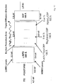
- the device includes a glass substrate, an anode layer (ITO), a hole transporting layer ( ⁇ -NPD), a hole blocking layer (BCP), an emission layer comprising a host (TAZ) and two phosphorescent dopants in separate bands or layers within the emission layer (Ir(ppy) 3 and Btp 2 Ir(acac)), an electron transporting layer comprising tris(8-hydroxyquinoline)aluminum ("Alq 3 "), and a cathode layer, wherein the cathode layer comprises a layer of lithium fluoride (“LiF”) and a layer of aluminum (“Al").
- Light emission from the emissive layer occurs when a voltage is applied across the cathode layer and the anode layer.
- the materials used in the device are an example of one embodiment of the invention, and may include any suitable materials which fulfill the function(s) of the respective layer(s).
- region may be used in some cases herein to refer to a region comprised of multiple layers or comprised of differently doped layers, alternatively referred to as bands, within the same region.
- the emissive region may be comprised of a single host material doped by a plurality of phosphorescent dopants with each phosphorescent dopant contained in a separate and distinct band, wherein the doped band within the emission region may be considered as a separate and distinct layer of host material with each separate and distinct layer being doped by a different phosphorescent dopant.
- the host material in one or more of these bands may be different from one band to the next.
- the emissive region may be comprised of a separate fluorescent layer and a host layer doped by one or more phosphorescent dopants.
- the emission region may comprise a host material doped by phosphorescent dopants, but the phosphorescent dopants may not be doped into separate and distinct bands. Rather, the doped region of one phosphorescent dopant may overlap the doped region of another phosphorescent dopant or the doped region of one phosphorescent dopant may be contained in its entirety within the doped region of another phosphorescent dopant. In fact, multiple layers may be used to achieve a combination of benefits, improving overall device efficiency.
- the materials listed below are provided for illustrative purposes only.
- the device is typically manufactured upon a substrate that may be a transparent or opaque material, such as glass, quartz, sapphire or plastic.
- the substrate may be, for example, rigid, flexible, conformable, and/or shaped to a desired configuration.
- a transparent cathode such as disclosed in U.S. Patent No. 5,703,436 , or co-pending U.S. Patent applications SIN 08/964,863 and 09/054,707 , may be used.
- a transparent cathode has light transmission characteristics such that the OLED has an optical transmission of at least about 50%.
- the transparent cathode has optical transmission characteristics that permit the OLED to have an optical transmission of at least about 70%, more preferably, at least about 85%.
- a top-emitting device is one for which light is produced only out of the top of the device and not through the substrate.
- the substrate and bottom electrode of such top-emitting devices may each be comprised of opaque and/or reflective materials, for example, with the electrode being a reflective thick metal layer.
- the substrate is typically referred to as being at the bottom of the device.
- a representative method of depositing the OLED layers is by thermal evaporation or organic vapor phase deposition (OVPD) such as disclosed in Baldo et al., "Organic Vapor Phase Deposition," Advanced Materials, vol. 10, no. 18 (1998) pp. 1505-1514 . If a polymer layer is used, the polymer may be spin coated.
- One representative method of depositing metal layers is by thermal or electron-beam evaporation.
- a representative method of depositing indium tin oxide is by electron-beam evaporation or sputtering.
- an electrophosphorescent OLED comprises an emissive region including a plurality of phosphorescent dopants, wherein each phosphorescent dopant is present in a band within the host emissive region, with the thickness of each band, the location of each band, and the concentration of each phosphorescent dopant within each band is adjusted such that a desired color and brightness of light are emitted from the OLED.
- the bands may be separate or overlapping.
- overlapping bands may employ a host material which impedes cascade energy transfer, improving device efficiency.
- the excitons may form, in an exciton formation zone, on one side of a hole blocking layer and diffuse through the hole blocking layer and into the emission region.
- the excitons may form either on the anode side of the emission layer or on the cathode side of the emission layer.
- the invention embodies efficient design and fabrication of devices that optimize the brightness, efficiency, color or a combination of these characteristics of the device by layering and ordering the layers within the emission region with respect to the location of the exciton formation zone.
- An alternative embodiment of the present invention comprises an emissive region including a plurality of phosphorescent dopants, wherein each of the phosphorescent dopants is mixed in at least a portion of the host material with one or more other phosphorescent dopants, wherein the host material is chosen to reduce cascade energy transfer, and the band thickness and concentration for each phosphorescent dopant is independently selected such that a desired color of light is emitted from the electrophosphorescent OLED.
- the present invention may be used to provide stable, efficient, high brightness, monochromatic, multicolor, or full-color, flat panel.displays of any size.
- the images created on such displays could be text or illustrations in full-color, in any resolution depending on the size of the individual OLEDs.
- Display devices of the present invention are therefore appropriate for an extremely wide variety of applications including billboards and signs, computer monitors or computer displays, and communications devices such as telephones, televisions, large area wall screens, theater screens and stadium screens.
- the structures described herein are included, for example, in a plurality of pixels in a light emitting device or as part of a single-pixel, flat panel backlight device or general light source for a room or office. Moreover, the structures described herein may be used as part of a laser device.
- the OLED would be incorporated into the laser as a light source.
- the present invention both has high efficiency and is capable of being tuned to transmit a specifically desired wavelength of light, which are both desirable characteristics for a laser light source.
- the light source could be incorporated into an organic laser inexpensively as a vacuum-deposited OLED.
- the phosphorescent-based OLEDs of the present invention may also be used as a light source for illumination applications.
- Such light sources could replace conventional incandescent or fluorescent lamps for certain types of illumination applications.
- Such phosphorescence-based OLEDs could be used, for example, in large backplane light sources that produce illumination of a desired color, including white light.
- Patent Application Nos. 08/779,141 ; 08/821,380 ; 08/977,205 ; 08/865,491 ; and 08/928,800 may also be used to prepare the OLEDs of the present invention.
- organic layers were deposited by high vacuum (10 -6 Torr) thermal evaporation onto a clean glass substrate precoated with indium tin oxide (ITO), which was used as the anode of the device and which had a sheet resistance of 20 ⁇ /square.
- ITO indium tin oxide
- the substrate Prior to film deposition, the substrate was solvent degreased and cleaned in a UV-ozone chamber before it was loaded into the deposition system.
- PEDOT:PSS poly(styrene sulphonic acid)
- One example of the invention is an efficient, organic white-light-emitting device, comprising, in sequence from the top (cathode side), an aluminum cathode layer (500 nm), a thin LiF electron injecting layer (0.5 nm), an Alq 3 electron transporting layer (50 nm), a vacuum-deposited emissive region of TAZ (30 nm), doped with a 20 nm thick band of phosphorescent red-emitting Btp 2 Ir(acac) at a concentration of 8 wt %, and a 10 nm thick band of phosphorescent green-emitting Ir(ppy) 3 at a concentration of 8 wt %.
- the emissive region was separated from the hole transporting layer by a hole-blocking layer of 2,9-dimethyl-4,7-diphenyl-1,10-phenanthroline (BCP) (6 nm), and a layer of ⁇ -NPD (50 nm), which had been vacuum-deposited onto the solvent degreased and cleaned layer of ITO.
- BCP 2,9-dimethyl-4,7-diphenyl-1,10-phenanthroline
- CIE Commission Internationale d'Eclairage
- the BCP layer substantially forces the hole-electron recombination to take place in the ⁇ -NPD layer with insignificant loss of holes through the BCP layer.
- the BCP layer then allows a large fraction of the triplet excitons thus formed to diffuse into the TAZ layer, so as to produce triplet excitons on the Btp 2 Ir(acac) and Ir(ppy) 3 molecules, which then emit visible light by phosphorescence.
- the BCP layer thus functions simultaneously as a hole blocking layer and as an exciton transporting layer, which is present between the phosphorescent zone of the device and the hole transporting region of the device where substantially all hole-electron recombination occurs, but where only a small fraction of the luminescence is produced as fluorescent emission.
- the emission may be tuned to produce substantially any desired color.
- the relative emissive contribution of each phosphorescent dopant, each producing a different color of light emission maybe controlled by adjusting the thickness of each layer and concentration of dopant in each layer, as required to generate a desired color of light emission from the electrophosphorescent OLED.
- triplet excitons that are responsible for phosphorescence have diffusion lengths of a hundred nanometers or more, whereas fluorescent, singlet excitons have diffusion lengths that seldom exceed ten nanometers. Therefore, a device using triplet excitons can achieve the brightness and efficiency necessary for a commercially useful device.
- blue, green and red phosphorescent emissive layers were combined in a multi-emissive-layer, organic light-emitting device to produce efficient white light.
- a blue phosphor iridium(III)bis(4,6-di-fluorophenyl)-pyridinato-N,C 2 ) picolinate (“FIrpic”) doped into 4,4'-N,N'-dicarbazole-biphenyl (CBP) was used as the blue emissive band, fac tris(2-phenylpyridine)iridium (Ir(ppy) 3 ) doped into CBP as the green emissive band and bis(2-(2'-benzo[4,5-a]thienyl)pyridinato-N,C 3 )iridium(acetylacetonate) (Btp 2 Ir(acac)) doped into CBP as the red emissive band.
- Another embodiment of this invention includes the process for fabricating a white light emitting OLED, having blue, green and red phosphorescent emissive layers combined in a multi-emissive-layer.
- OLEDs were grown on a glass substrate pre-coated with an indium-tin-oxide (ITO) layer having a sheet resistance of 20- ⁇ /sq. Prior to any organic layer deposition or coating, the substrate was degreased with solvents and then treated with an oxygen plasma for 8 minutes with 20W at 150 mTorr. Poly(ethylene-dioxythiophene)/poly(styrene sulphonic acid) (PEDOT:PSS) was spun onto the ITO at 4000 rpm for 40s and then baked for 10 mins.
- PEDOT:PSS Poly(ethylene-dioxythiophene)/poly(styrene sulphonic acid)
- an emissive region consisting of a 10nm-thick layer of 4,4'-N,N'-dicarbazole-biphenyl (CBP) doped with 8 wt.% of iridium(III)bis(4,6-di-fluorophenyl)-pyridinato-N,C 2 ) picolinate (FIrpic), followed by a 10nm-thick CBP layer doped with 8 wt.% bis(2-(2'-benzo[4,5-a]thienyl)pyrxdinato-N,C 3 )iridium(acetylacetonate) Btp 2 Ir(acac) layer and then by a 10-nm-thick layer of CBP doped with 8 wt.% fac tris(2-phenylpyridine)iridium (Ir(ppy) 3 ) was grown.
- EMR emissive region
- the emission color and device efficiency was found to depend on the order in which the layers were doped, and white emission was obtained using the process described here.
- a 10nm-thick 2,9-dimethyl-4,7-diphenyl-1,10-phenanthroline (BCP) electron transporting/hole blocking layer (ETL) was the final organic layer deposited.
- BCP 2,9-dimethyl-4,7-diphenyl-1,10-phenanthroline
- ETL electron transporting/hole blocking layer
- the evaporation chamber was vented with nitrogen and the sample was transferred under a nitrogen atmosphere containing ⁇ 1 ppm of water and oxygen to a nitrogen glove box in which a shadow mask with Imm-diameter openings was affixed to the sample.
- a cathode consisting of a 5 ⁇ -thick LiF layer followed by 100nm of A1 was deposited. The sample was only exposed to air when it was being tested.
- the device structure is shown in Figure 9 .
- the device in Figure 9 can effectively produce white light.
- the rates of radiative (k r ) and non-radiative (k nr ) recombination, diffusivity constants, and resonance energy transfer rates (k tr ) between hosts and guests are variables to consider for each layer in the device.
- concentration of the dopants By varying the concentration of the dopants, by varying the location of the different color regions with respect to the interface where exciton formation occurs, and by independently changing the thickness of each of the layers, the inventors were able to tune the color/CIE coordinates of a multi-emissive layer OLED.
- the concentration of the phosphorescent dopants were kept approximately constant at about (8 ⁇ 2) wt.% in order to achieve both an efficient and thin device.
- k r and the rate of transfer between the host and phosphor is maximized at doping levels between about 6 wt.% and 9 wt.%.
- Lower doping levels have lower k tr and concentration quenching decreases k r at higher doping levels.
- excitons form at the interface between two materials where a build up of excess charge occurs in one of the materials. Excess charge is usually present in one of the materials due to order of magnitude differences in mobility between the materials or large energy barriers to charge transfer at interfaces.
- the location of the exciton zone of formation (EZF) for the multi-emissive layer structure affects the color and efficiency of the device; therefore, it is important to the device design.
- the ratio of k nr to k r or its reciprocal for each of the individual emissive layers can be used to determine the placement of each of the emissive layers with respect to the EZF.
- the emissive layers were ordered in such a manner that the ratio of k nr to k r was highest near the EZF and lowest far from the EZF. It is believed that this layer arrangement improved the device efficiency of the white light emitting, electrophosphorescent OLED.
- a preferred embodiment of the invention placed an FIrpic:CBP layer with a concentration of about 8 wt.% at this interface to improve the efficiency of the white light emitting OLED.
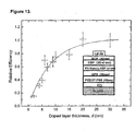
- Results for this preferred embodiment of the present invention having a layer thickness of about 10 nm for each of the emissive layers and stacked in the order shown in Figure 9 , had a CIE coordinate of (0.31, 0.35).
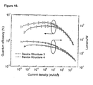
- the external quantum efficiency of the device is shown as a function of its current density in Figure 12 .
- ⁇ p yields a value of ⁇ p equal to (4.0 ⁇ 0.4) % and a luminance of (3.3 ⁇ 0.3) lm/W or (36 000 ⁇ 4 000) cd/m 2 at 15.8 V.
- the external quantum efficiency was at least 3.0% over a corresponding current density of three orders of magnitude, as shown in Figure 12 .
- the inventors believe that the comparatively low external efficiency at low values of current density might be caused by current leakage; whereas, at high current densities J > 10 mA/cm 2 , the roll-off has been previously ascribed to triplet-triplet annihilation.
- the break in vacuum which was in this embodiment of the invention to add the cathode, also limited the device efficiency, because the vacuum break would tend to introduce non-radiative defect states during exposure to the nitrogen atmosphere.
- the inventors would expect even higher device efficiencies using ultrahigh vacuum conditions throughout the fabrication process.
- the cathode layer is deposited without any break in the ultrahigh vacuum environment.
- PDOT:PSS Poly(ethylene-dioxythiophene):poly(styrene sulphonic acid)
- PEDOT:PSS Poly(styrene sulphonic acid)
- ITO ITO
- PSS poly(styrene sulphonic acid)
- Deposition began with a 30 nm-thick 4,4'-bis[N-(1-napthyl)-N-pbenyl-amino]biphenyl ( ⁇ -NPD) hole transport layer (HTL).
- an emissive region was grown consisting of a 20 nm-thick layer of the primarily electron conducting host 4,4'-N,N'-dicarbazole-biphenyl (CBP) doped with 6 wt% of the blue emitting phosphor, iridium(III)bis(4,6-di-fluorophenyl)-pyridinato-N,C 2 ) picolinate (FIrpic), followed by a 2 nm-thick CBP layer doped at 8 wt% with the red phosphor; bis(2-(2'-beozo[4,5-a]thienyl)pyridinato-N,C 3 ) iridium(acetylacetonate) (Btp 2 Ir(acac)), and a 2 nm-thick CBP layer doped at 8 wt% with the yellow phosphor; bis(2-phenyl benzothiozolato-N,C 2 )iridium(
- BCP was the final organic layer deposited on all devices and served as both a hole/exciton blocker and an electron transport layer (ETL).
- ETL electron transport layer
- the samples were transferred from the evaporation chamber into a N 2 filled glove box containing ⁇ 1 ppm of H 2 O and O 2 .
- the cathode consisted of 5 ⁇ of LiF followed by 100 nm of Al.
- PDOT:PSS Poly(ethylene-dioxythiophene):poly(styrene sulphonic acid)
- PEDOT:PSS Poly(styrene sulphonic acid)
- ITO ITO
- PSS poly(styrene sulphonic acid)
- Deposition began with a 30 nm-thick 4,4'-bis[N-(1-napthyl)-N-phenyl-amino]biphenyl ( ⁇ -NPD) hole transport layer (HTL).
- the EMR consisted of a 20 nm-thick layer of CBP doped with 6 wt% of FIrpic, followed by a 3 nm-thick 2,9-dimethyl-4,7-diphenyl-1,10-phenanthroline (BCP) exciton blocking layer, and a 10 nm-thick CBP layer doped with 8 wt% Btp 2 Ir(acac).
- BCP was the final organic layer deposited on all devices and served as both a hole/exciton blocker and an electron transport layer (ETL). After deposition of the organic layers, the samples were transferred from the evaporation chamber into a N 2 filled glove box containing ⁇ 1 ppm of H 2 O and O 2 .
- the cathode consisted of 5 ⁇ of LiF followed by 100 nm of Al.
- triplet excitons provide a means for obtaining the desired color balance.
- Triplets have lifetimes that are several orders of magnitude longer than singlets, hence they have longer diffusion lengths, allowing emissive layers to be >10 nm thick.
- the thickness of each layer doped with a different phosphor can be adjusted to serve as a recombination zone of the appropriate fraction of excitons initially formed at the HTL/EMR interface.
- the CBP triplet exciton diffusion length, L D is first determined. This is done by varying the thickness ( d ) of a fac tris(2-phenylpyridine)iridium (Ir(ppy) 3 ) phosphor doped region within a 30 nm thick CBP layer in the structure shown in Figure 13 . The efficiencies of the various devices are then compared to the efficiency of a device with the entire CBP region doped with Ir(ppy) 3 .
- ⁇ ( d ) is the efficiency of a device with a doped CBP layer of thickness d
- the CIE coordinates of the OLED emission can be tuned over a wide range.
- the phosphors with lower triplet energy and which therefore trap excitons most readily should be positioned farthest from the exciton formation region. This ensures that the excitons can diffuse throughout the luminescent region, producing the desired output color balance.
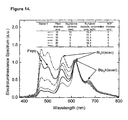
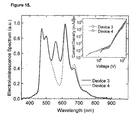
- Figure 14 shows the dependence of electrophosphorescent spectrum of Device 3 on layer thickness, phosphor doping concentration, and the insertion of a blocking layer between the Flrpic and Btp 2 Ir(acac) doped regions. All spectra were recorded at 10 mA/cm 2 , corresponding to luminances ranging between 400- and 800 cd/m 2 .
- Flrpic emission does not increase relative to Btp 2 Ir(acac) emission for FIrpic doped layer thicknesses exceeding 30 nm.
- the color balance can be improved by inserting a thin BCP, hole/exciton blocking layer between the FIrpic and Btp 2 Ir(acac) doped layers in Device 4.
- This layer retards the flow of holes from the Flrpic doped layer towards the cathode and thereby forces more excitons to form in the FIrpic layer, and it prevents excitons from diffusing towards the cathode after forming in the FIrpic doped layer.
- the transfer of triplets between the host and guest molecules is hindered because fewer guest molecules are within the Förster transfer radius ( ⁇ 30 ⁇ ) of the host, decreasing proportionately the fraction of Bt 2 Ir(acac) emission.
- ⁇ (2) ⁇ ⁇ (10) because the dopant can capture more of the CBP triplets for thicker doped regions.
- the emission from a 2 nm thick Bt 2 Ir(acac) doped layer should be lower than for a 10 nm thick layer because it captures fewer CBP excitons.
- Device 3 and 4 electroluminescent spectra are compared in Figure 15 .
- the enhancement of the yellow region of the spectrum for Device 3 increases the CRI from 50 to 83 and shifts the CIE from (0.35,0.36) to (0.37,0.40) relative to Device 4.
- the x and y CIE coordinates of all the devices varied by ⁇ 10% between 1 mA/cm 2 and 500 mA/cm 2 , corresponding to luminances in the range from 60- to 20 000 cd/m 2 .
- Device 4 is useful for flat-panel displays since the human perception of white from the display will be unaffected by the lack of emission in the yellow region of the spectrum.
- the best white that can be made with FIirpic and Btp 2 Ir(acac) doped into CBP is at (0.33, 0.32), close to that of Device 4 of (0.35,0.36).
- Device 3 With a CRI of 83, Device 3 can be used in flat-panel displays, but it can also be used as an illumination source, since at this high a CRI value, objects will appear as they would under daylight conditions.
- the CRI of Device 4 can be theoretically improved to a maximum value of 88, however, the CIE of such an optimized device is (0.47,0.40).
- the additional doped layer also improves the efficiency of Device 4 as compared to Device 3 by boosting the yellow emission where the human eye has the highest photopic efficiency, and by the use of Bt 2 Ir(acac) which has a higher ⁇ ext than FIrpic.
Landscapes
- Chemical & Material Sciences (AREA)
- Physics & Mathematics (AREA)
- Optics & Photonics (AREA)
- Engineering & Computer Science (AREA)
- Materials Engineering (AREA)
- Organic Chemistry (AREA)
- Electroluminescent Light Sources (AREA)
- Electrochromic Elements, Electrophoresis, Or Variable Reflection Or Absorption Elements (AREA)
- Luminescent Compositions (AREA)
- Optical Filters (AREA)
Priority Applications (2)
| Application Number | Priority Date | Filing Date | Title |
|---|---|---|---|
| EP14186883.6A EP2822019B1 (en) | 2001-05-16 | 2002-05-13 | High efficiency multi-color electro-phosphorescent OLEDs |
| EP18151943.0A EP3333876A1 (en) | 2001-05-16 | 2002-05-13 | High efficiency multi-color electro-phosphorescent oleds |
Applications Claiming Priority (2)
| Application Number | Priority Date | Filing Date | Title |
|---|---|---|---|
| US29149601P | 2001-05-16 | 2001-05-16 | |
| EP02734378.9A EP1390962B2 (en) | 2001-05-16 | 2002-05-13 | High efficiency multi-color electro-phosphorescent oleds |
Related Parent Applications (3)
| Application Number | Title | Priority Date | Filing Date |
|---|---|---|---|
| EP02734378.9 Division | 2002-05-13 | ||
| EP02734378.9A Division EP1390962B2 (en) | 2001-05-16 | 2002-05-13 | High efficiency multi-color electro-phosphorescent oleds |
| EP02734378.9A Division-Into EP1390962B2 (en) | 2001-05-16 | 2002-05-13 | High efficiency multi-color electro-phosphorescent oleds |
Related Child Applications (2)
| Application Number | Title | Priority Date | Filing Date |
|---|---|---|---|
| EP18151943.0A Division EP3333876A1 (en) | 2001-05-16 | 2002-05-13 | High efficiency multi-color electro-phosphorescent oleds |
| EP14186883.6A Division EP2822019B1 (en) | 2001-05-16 | 2002-05-13 | High efficiency multi-color electro-phosphorescent OLEDs |
Publications (3)
| Publication Number | Publication Date |
|---|---|
| EP2259285A2 EP2259285A2 (en) | 2010-12-08 |
| EP2259285A3 EP2259285A3 (en) | 2011-03-23 |
| EP2259285B1 true EP2259285B1 (en) | 2014-10-22 |
Family
ID=23120527
Family Applications (4)
| Application Number | Title | Priority Date | Filing Date |
|---|---|---|---|
| EP10181013.3A Expired - Lifetime EP2259285B1 (en) | 2001-05-16 | 2002-05-13 | High efficiency multi-color electro-phosphorescent OLEDs. |
| EP18151943.0A Ceased EP3333876A1 (en) | 2001-05-16 | 2002-05-13 | High efficiency multi-color electro-phosphorescent oleds |
| EP02734378.9A Expired - Lifetime EP1390962B2 (en) | 2001-05-16 | 2002-05-13 | High efficiency multi-color electro-phosphorescent oleds |
| EP14186883.6A Expired - Lifetime EP2822019B1 (en) | 2001-05-16 | 2002-05-13 | High efficiency multi-color electro-phosphorescent OLEDs |
Family Applications After (3)
| Application Number | Title | Priority Date | Filing Date |
|---|---|---|---|
| EP18151943.0A Ceased EP3333876A1 (en) | 2001-05-16 | 2002-05-13 | High efficiency multi-color electro-phosphorescent oleds |
| EP02734378.9A Expired - Lifetime EP1390962B2 (en) | 2001-05-16 | 2002-05-13 | High efficiency multi-color electro-phosphorescent oleds |
| EP14186883.6A Expired - Lifetime EP2822019B1 (en) | 2001-05-16 | 2002-05-13 | High efficiency multi-color electro-phosphorescent OLEDs |
Country Status (9)
| Country | Link |
|---|---|
| US (2) | US7009338B2 (ja) |
| EP (4) | EP2259285B1 (ja) |
| JP (1) | JP4493915B2 (ja) |
| KR (1) | KR100888424B1 (ja) |
| CN (1) | CN1302565C (ja) |
| AT (1) | ATE498898T1 (ja) |
| AU (1) | AU2002305548A1 (ja) |
| DE (1) | DE60239198D1 (ja) |
| WO (1) | WO2002091814A2 (ja) |
Families Citing this family (217)
| Publication number | Priority date | Publication date | Assignee | Title |
|---|---|---|---|---|
| KR100721656B1 (ko) | 2005-11-01 | 2007-05-23 | 주식회사 엘지화학 | 유기 전기 소자 |
| JP4048521B2 (ja) * | 2000-05-02 | 2008-02-20 | 富士フイルム株式会社 | 発光素子 |
| US7306856B2 (en) | 2000-07-17 | 2007-12-11 | Fujifilm Corporation | Light-emitting element and iridium complex |
| ATE482476T1 (de) * | 2000-07-17 | 2010-10-15 | Fujifilm Corp | Lichtemittierendes element und azolverbindung |
| US6893743B2 (en) * | 2000-10-04 | 2005-05-17 | Mitsubishi Chemical Corporation | Organic electroluminescent device |
| AU2002222565A1 (en) * | 2000-11-30 | 2002-06-11 | Canon Kabushiki Kaisha | Luminescent element and display |
| WO2002091814A2 (en) * | 2001-05-16 | 2002-11-21 | The Trustees Of Princeton University | High efficiency multi-color electro-phosphorescent oleds |
| US7102632B2 (en) * | 2001-06-05 | 2006-09-05 | Eastman Kodak Company | Method for saving power in an organic electroluminescent display |
| EP1399002A4 (en) * | 2001-06-15 | 2007-11-21 | Canon Kk | ORGANIC ELECTROLUMINESCENCE DEVICE |
| JP2003123982A (ja) * | 2001-08-07 | 2003-04-25 | Fuji Photo Film Co Ltd | 発光素子及び新規イリジウム錯体 |
| US6869695B2 (en) * | 2001-12-28 | 2005-03-22 | The Trustees Of Princeton University | White light emitting OLEDs from combined monomer and aggregate emission |
| US6863997B2 (en) * | 2001-12-28 | 2005-03-08 | The Trustees Of Princeton University | White light emitting OLEDs from combined monomer and aggregate emission |
| US6951694B2 (en) | 2002-03-29 | 2005-10-04 | The University Of Southern California | Organic light emitting devices with electron blocking layers |
| JP3902981B2 (ja) * | 2002-06-04 | 2007-04-11 | キヤノン株式会社 | 有機発光素子及び表示装置 |
| US7332739B2 (en) * | 2002-06-20 | 2008-02-19 | Samsung Sdi Co., Ltd. | Organic electroluminescent device using mixture of phosphorescent material as light-emitting substance |
| KR100478524B1 (ko) * | 2002-06-28 | 2005-03-28 | 삼성에스디아이 주식회사 | 고분자 및 저분자 발광 재료의 혼합물을 발광 재료로사용하는 유기 전계 발광 소자 |
| US7265378B2 (en) | 2002-07-10 | 2007-09-04 | E. I. Du Pont De Nemours And Company | Electronic devices made with electron transport and/or anti-quenching layers |
| KR100650046B1 (ko) * | 2002-11-20 | 2006-11-27 | 엘지전자 주식회사 | 고효율의 유기 전계 발광 소자 |
| JP5104816B2 (ja) * | 2002-11-26 | 2012-12-19 | コニカミノルタホールディングス株式会社 | 有機エレクトロルミネッセンス素子及びそれを有する表示装置 |
| US7063900B2 (en) * | 2002-12-23 | 2006-06-20 | General Electric Company | White light-emitting organic electroluminescent devices |
| AU2003290341A1 (en) * | 2002-12-24 | 2004-07-22 | Elam-T Limited | Electroluminescent materials and devices |
| JP4942934B2 (ja) * | 2002-12-25 | 2012-05-30 | 富士フイルム株式会社 | 有機エレクトロルミネッセンス素子及び有機エレクトロルミネッセンスディスプレイ |
| WO2004060026A1 (ja) | 2002-12-26 | 2004-07-15 | Semiconductor Energy Laboratory Co., Ltd. | 有機発光素子 |
| KR100543478B1 (ko) | 2002-12-31 | 2006-01-20 | 엘지.필립스 엘시디 주식회사 | 유기전계 발광소자와 그 제조방법 |
| JP2004227814A (ja) * | 2003-01-20 | 2004-08-12 | Korai Kagi Kofun Yugenkoshi | 有機発光装置及びその製造方法 |
| JP3966283B2 (ja) * | 2003-01-28 | 2007-08-29 | セイコーエプソン株式会社 | 発光体とその製造方法及び製造装置、電気光学装置並びに電子機器 |
| US6900458B2 (en) | 2003-02-21 | 2005-05-31 | Universal Display Corporation | Transflective display having an OLED backlight |
| JP4526776B2 (ja) * | 2003-04-02 | 2010-08-18 | 株式会社半導体エネルギー研究所 | 発光装置及び電子機器 |
| US20040209116A1 (en) * | 2003-04-21 | 2004-10-21 | Xiaofan Ren | Organic light emitting devices with wide gap host materials |
| EP1617710B1 (en) * | 2003-04-23 | 2015-05-20 | Konica Minolta Holdings, Inc. | Material for organic electroluminescent device, organic electroluminescent device, illuminating device and display |
| DE10326725A1 (de) * | 2003-06-10 | 2005-01-13 | Samsung SDI Co., Ltd., Suwon | OLED-Bauelement und Display auf Basis von OLED-Bauelementen mit verbesserter Effizienz |
| US6987355B2 (en) * | 2003-06-11 | 2006-01-17 | Eastman Kodak Company | Stacked OLED display having improved efficiency |
| US6903378B2 (en) * | 2003-06-26 | 2005-06-07 | Eastman Kodak Company | Stacked OLED display having improved efficiency |
| US7211823B2 (en) * | 2003-07-10 | 2007-05-01 | Universal Display Corporation | Organic light emitting device structure for obtaining chromaticity stability |
| DE10333232A1 (de) * | 2003-07-21 | 2007-10-11 | Merck Patent Gmbh | Organisches Elektrolumineszenzelement |
| CN1820548A (zh) * | 2003-07-28 | 2006-08-16 | 出光兴产株式会社 | 白色系有机电致发光元件 |
| JP2005100921A (ja) | 2003-08-22 | 2005-04-14 | Sony Corp | 有機el素子および表示装置 |
| KR100544126B1 (ko) * | 2003-08-26 | 2006-01-23 | 삼성에스디아이 주식회사 | 유기 전계 발광 소자 및 그 제조방법 |
| KR100560783B1 (ko) * | 2003-09-03 | 2006-03-13 | 삼성에스디아이 주식회사 | 도핑된 발광층을 갖는 유기전계발광소자 |
| DE10340711A1 (de) * | 2003-09-04 | 2005-04-07 | Covion Organic Semiconductors Gmbh | Elektronische Vorrichtung enthaltend organische Halbleiter |
| DE112004001737B4 (de) * | 2003-09-17 | 2016-08-11 | The Regents Of The University Of California | Verfahren umfassend lösliche, konjugierte Polymere zur Ausbildung benachbarter Schichten auf einem Substrat oder zum Hinzufügen einer Polymerschicht zu einem Substrat, mehrschichtige elektronische Vorrichtung und Verwendung in elektronischen Bauteilen |
| US6881502B2 (en) * | 2003-09-24 | 2005-04-19 | Eastman Kodak Company | Blue organic electroluminescent devices having a non-hole-blocking layer |
| US7830085B2 (en) * | 2003-10-06 | 2010-11-09 | The Regents Of The University Of California | White electrophosphorescence from semiconducting polymer blends |
| WO2005053051A1 (de) * | 2003-11-25 | 2005-06-09 | Merck Patent Gmbh | Organisches elektrolumineszenzelement |
| US7374828B2 (en) * | 2003-12-05 | 2008-05-20 | Eastman Kodak Company | Organic electroluminescent devices with additive |
| US7084425B2 (en) * | 2003-12-05 | 2006-08-01 | Eastman Kodak Company | Organic electroluminescent devices |
| US20050123791A1 (en) * | 2003-12-05 | 2005-06-09 | Deaton Joseph C. | Organic electroluminescent devices |
| US20050158582A1 (en) * | 2004-01-15 | 2005-07-21 | Fuji Photo Film Co., Ltd. | Organic electroluminescent element |
| US7629061B2 (en) * | 2004-01-16 | 2009-12-08 | Osram Opto Semiconductors Gmbh | Heterostructure devices using cross-linkable polymers |
| KR100657892B1 (ko) * | 2004-02-11 | 2006-12-14 | 삼성에스디아이 주식회사 | 유기 전계 발광 소자 |
| TW200541401A (en) | 2004-02-13 | 2005-12-16 | Idemitsu Kosan Co | Organic electroluminescent device |
| WO2005081587A1 (ja) * | 2004-02-19 | 2005-09-01 | Idemitsu Kosan Co., Ltd. | 白色系有機エレクトロルミネッセンス素子 |
| JP2005310742A (ja) * | 2004-03-25 | 2005-11-04 | Sanyo Electric Co Ltd | 有機エレクトロルミネッセンス素子 |
| JP4621201B2 (ja) * | 2004-03-25 | 2011-01-26 | 出光興産株式会社 | 有機エレクトロルミネッセンス素子 |
| KR101110890B1 (ko) * | 2004-04-02 | 2012-03-13 | 이데미쓰 고산 가부시키가이샤 | 전자 장벽층을 개재시킨 2개의 발광층을 갖는 유기전기발광 소자 |
| KR100647598B1 (ko) * | 2004-04-06 | 2006-11-23 | 삼성에스디아이 주식회사 | 유기 전계 발광 소자 및 그 제조방법 |
| US7361415B2 (en) * | 2004-04-16 | 2008-04-22 | The University Of Hong Kong | System and method for producing light with organic light-emitting devices |
| JP4429067B2 (ja) * | 2004-04-21 | 2010-03-10 | 富士フイルム株式会社 | 有機電界発光素子 |
| US20050244672A1 (en) * | 2004-04-30 | 2005-11-03 | Chi-Ming Che | Organic light-emitting devices |
| JP4737086B2 (ja) * | 2004-05-31 | 2011-07-27 | 株式会社豊田自動織機 | 有機el素子 |
| JP4631316B2 (ja) * | 2004-06-07 | 2011-02-16 | パナソニック株式会社 | エレクトロルミネセンス素子 |
| JP2006054422A (ja) * | 2004-07-15 | 2006-02-23 | Fuji Photo Film Co Ltd | 有機電界発光素子及び表示素子 |
| WO2006008977A1 (ja) * | 2004-07-16 | 2006-01-26 | Konica Minolta Holdings, Inc. | 有機エレクトロルミネッセンス素子、画像表示素子および照明装置 |
| WO2006009024A1 (ja) * | 2004-07-23 | 2006-01-26 | Konica Minolta Holdings, Inc. | 有機エレクトロルミネッセンス素子、表示装置及び照明装置 |
| US7316756B2 (en) | 2004-07-27 | 2008-01-08 | Eastman Kodak Company | Desiccant for top-emitting OLED |
| EP1789994A1 (de) * | 2004-08-13 | 2007-05-30 | Novaled AG | Schichtanordnung für ein lichtemittierendes bauelement |
| US20060042685A1 (en) * | 2004-08-25 | 2006-03-02 | Ying Wang | Electronic devices having a charge transport layer that has defined triplet energy level |
| EP1825532B1 (en) * | 2004-08-27 | 2013-04-24 | Showa Denko K.K. | Organic electroliminescent device and production method thereof |
| WO2006029231A1 (en) * | 2004-09-03 | 2006-03-16 | The Regents Of The University Of California | Soluble conjugated polymers |
| US9040170B2 (en) * | 2004-09-20 | 2015-05-26 | Global Oled Technology Llc | Electroluminescent device with quinazoline complex emitter |
| GB0422391D0 (en) * | 2004-10-08 | 2004-11-10 | Cambridge Display Tech Ltd | Light emitting device |
| US7776456B2 (en) * | 2004-12-03 | 2010-08-17 | Universal Display Corporation | Organic light emitting devices with an emissive region having emissive and non-emissive layers and method of making |
| KR100700641B1 (ko) * | 2004-12-03 | 2007-03-27 | 삼성에스디아이 주식회사 | 레이저 조사 장치, 패터닝 방법 및 그를 이용한 레이저열전사 패터닝 방법과 이를 이용한 유기 전계 발광 소자의제조 방법 |
| JP4496949B2 (ja) * | 2004-12-13 | 2010-07-07 | 株式会社豊田自動織機 | 有機el素子 |
| US20060145599A1 (en) * | 2005-01-04 | 2006-07-06 | Reza Stegamat | OLEDs with phosphors |
| US7564180B2 (en) * | 2005-01-10 | 2009-07-21 | Cree, Inc. | Light emission device and method utilizing multiple emitters and multiple phosphors |
| KR20060084733A (ko) * | 2005-01-20 | 2006-07-25 | 삼성에스디아이 주식회사 | 유기 전계 발광 소자 및 이의 제조 방법 |
| JP5030798B2 (ja) * | 2005-03-01 | 2012-09-19 | エージェンシー フォー サイエンス、テクノロジー アンド リサーチ | 溶液加工した有機金属錯体および電界発光素子における溶液加工した有機金属錯体の使用 |
| GB2472526B (en) * | 2005-03-02 | 2011-03-23 | Konica Minolta Holdings Inc | Organic electroluminescence element, image display unit and lighting device |
| US7554257B2 (en) * | 2005-03-02 | 2009-06-30 | Osram Opto Semiconductors Gmbh | Method to generate high efficient devices which emit high quality light for illumination |
| US20090051273A1 (en) * | 2005-03-02 | 2009-02-26 | Konica Minolta Holdings, Inc. | Organic Electroluminescence Element, Image Display Device and Lighting Device |
| WO2006095553A1 (ja) * | 2005-03-04 | 2006-09-14 | Konica Minolta Holdings, Inc. | 有機エレクトロルミネッセンス素子、表示装置、液晶表示装置及び照明装置 |
| EP1705727B1 (de) | 2005-03-15 | 2007-12-26 | Novaled AG | Lichtemittierendes Bauelement |
| US20060216544A1 (en) * | 2005-03-23 | 2006-09-28 | Fuji Photo Film Co. Ltd | Organic electroluminescent device |
| US8017251B2 (en) | 2005-03-28 | 2011-09-13 | Fujifilm Corporation | Organic electroluminescent device |
| JP2006310748A (ja) * | 2005-03-28 | 2006-11-09 | Fuji Photo Film Co Ltd | 有機電界発光素子 |
| US7560729B2 (en) | 2005-03-30 | 2009-07-14 | Fujifilm Corporation | Organic electroluminescent device for improved luminous efficiency and chromaticity |
| US9070884B2 (en) | 2005-04-13 | 2015-06-30 | Universal Display Corporation | Hybrid OLED having phosphorescent and fluorescent emitters |
| US8057916B2 (en) | 2005-04-20 | 2011-11-15 | Global Oled Technology, Llc. | OLED device with improved performance |
| US7511418B2 (en) * | 2005-05-20 | 2009-03-31 | Semiconductor Energy Laboratory Co., Ltd. | Light emitting element, light emitting device and manufacturing method of light emitting element |
| US7474048B2 (en) * | 2005-06-01 | 2009-01-06 | The Trustees Of Princeton University | Fluorescent filtered electrophosphorescence |
| TWI471058B (zh) * | 2005-06-01 | 2015-01-21 | Univ Princeton | 螢光之經過濾電磷光作用 |
| CN100421278C (zh) * | 2005-06-02 | 2008-09-24 | 友达光电股份有限公司 | 有机发光二极管的发光层及应用其的有机发光二极管显示面板 |
| KR101330672B1 (ko) | 2005-06-10 | 2013-11-18 | 톰슨 라이센싱 | 서로 다른 유기 물질의 2개 이하의 층을 포함하는 발광 유기 다이오드 |
| KR20080025393A (ko) * | 2005-07-06 | 2008-03-20 | 이데미쓰 고산 가부시키가이샤 | 유기 전계 발광 소자 |
| KR20070009306A (ko) * | 2005-07-15 | 2007-01-18 | 삼성에스디아이 주식회사 | 백색 유기 발광 소자의 제조 방법 |
| JP4959961B2 (ja) * | 2005-07-29 | 2012-06-27 | 株式会社ジャパンディスプレイセントラル | 有機el素子の製造方法 |
| TWI279165B (en) * | 2005-08-09 | 2007-04-11 | Au Optronics Corp | White organic light emitting diode |
| KR20070019496A (ko) * | 2005-08-12 | 2007-02-15 | 삼성에스디아이 주식회사 | 백색 유기 발광 소자 및 그의 제조방법 |
| JP2007088251A (ja) * | 2005-09-22 | 2007-04-05 | Toshiba Matsushita Display Technology Co Ltd | 有機el素子及び有機el表示装置 |
| US8148891B2 (en) * | 2005-10-04 | 2012-04-03 | Universal Display Corporation | Electron impeding layer for high efficiency phosphorescent OLEDs |
| EP1936714A1 (en) * | 2005-10-11 | 2008-06-25 | Konica Minolta Holdings, Inc. | Organic electroluminescent device, liquid crystal display and illuminating device |
| US8956738B2 (en) | 2005-10-26 | 2015-02-17 | Global Oled Technology Llc | Organic element for low voltage electroluminescent devices |
| US8310146B2 (en) * | 2005-10-27 | 2012-11-13 | Konica Minolta Holdings, Inc. | Organic electroluminescent device, liquid crystal display and illuminating device |
| US9666826B2 (en) | 2005-11-30 | 2017-05-30 | Global Oled Technology Llc | Electroluminescent device including an anthracene derivative |
| US20070122657A1 (en) * | 2005-11-30 | 2007-05-31 | Eastman Kodak Company | Electroluminescent device containing a phenanthroline derivative |
| JP4251331B2 (ja) * | 2005-12-27 | 2009-04-08 | カシオ計算機株式会社 | 表示装置の製造装置及び表示装置の製造方法 |
| JP4904821B2 (ja) * | 2006-01-12 | 2012-03-28 | コニカミノルタホールディングス株式会社 | 有機エレクトロルミネッセンス素子および有機エレクトロルミネッセンスディスプレイ |
| WO2007083918A1 (en) | 2006-01-18 | 2007-07-26 | Lg Chem. Ltd. | Oled having stacked organic light-emitting units |
| US8518556B2 (en) * | 2006-01-27 | 2013-08-27 | Konica Minolta Holdings, Inc. | Electroluminescent element |
| US8008856B2 (en) * | 2006-04-19 | 2011-08-30 | Massachusetts Institute Of Technology | Light emitting devices with agent to increase the fraction of excitons formed as a singlet |
| EP2016633A1 (en) | 2006-05-08 | 2009-01-21 | Eastman Kodak Company | Oled electron-injecting layer |
| US7579773B2 (en) * | 2006-06-05 | 2009-08-25 | The Trustees Of Princeton University | Organic light-emitting device with a phosphor-sensitized fluorescent emission layer |
| US8105161B2 (en) * | 2006-07-17 | 2012-01-31 | Wms Gaming Inc. | Wagering game machine with OLED transmissive LCD |
| JP5205584B2 (ja) | 2006-09-06 | 2013-06-05 | ユー・ディー・シー アイルランド リミテッド | 有機電界発光素子および表示装置 |
| US7800295B2 (en) * | 2006-09-15 | 2010-09-21 | Universal Display Corporation | Organic light emitting device having a microcavity |
| US9012034B2 (en) * | 2006-09-28 | 2015-04-21 | Udc Ireland Limited | Organic electroluminescence element |
| DE102006048202A1 (de) * | 2006-10-11 | 2008-04-17 | Universität Regensburg | Lanthanoid-Emitter für OLED-Anwendungen |
| US8945722B2 (en) * | 2006-10-27 | 2015-02-03 | The University Of Southern California | Materials and architectures for efficient harvesting of singlet and triplet excitons for white light emitting OLEDs |
| WO2008069153A1 (en) * | 2006-12-04 | 2008-06-12 | Semiconductor Energy Laboratory Co., Ltd. | Light-emitting element, light-emitting device, and electronic device |
| JP4254856B2 (ja) * | 2006-12-22 | 2009-04-15 | ソニー株式会社 | 有機電界発光素子および表示装置 |
| WO2009030981A2 (en) * | 2006-12-28 | 2009-03-12 | Universal Display Corporation | Long lifetime phosphorescent organic light emitting device (oled) structures |
| KR101407574B1 (ko) * | 2007-01-12 | 2014-06-17 | 삼성디스플레이 주식회사 | 백색 유기 발광 소자 |
| KR101359632B1 (ko) * | 2007-01-19 | 2014-02-19 | 삼성디스플레이 주식회사 | 백색 유기 발광 소자 |
| CN101247297B (zh) * | 2007-02-16 | 2010-07-14 | 华为技术有限公司 | 对家庭网络中应用终端进行自动配置的装置、系统和方法 |
| KR20080083881A (ko) | 2007-03-13 | 2008-09-19 | 삼성전자주식회사 | 색 조절층을 구비한 백색 유기발광소자 |
| TW200908777A (en) | 2007-03-23 | 2009-02-16 | Idemitsu Kosan Co | Organic el device |
| US20090001875A1 (en) * | 2007-06-29 | 2009-01-01 | Yun Chi | Organic light-emitting device incorporating multifunctional osmium complexes |
| JP2009037981A (ja) * | 2007-08-03 | 2009-02-19 | Idemitsu Kosan Co Ltd | 有機el素子および有機el素子の製造方法 |
| DE102007053396A1 (de) * | 2007-08-07 | 2009-02-12 | Osram Opto Semiconductors Gmbh | Strahlungsemittierende Vorrichtung |
| JP5530608B2 (ja) * | 2007-09-13 | 2014-06-25 | 株式会社半導体エネルギー研究所 | 発光素子および発光装置 |
| JP5669580B2 (ja) * | 2007-09-20 | 2015-02-12 | ビーエーエスエフ ソシエタス・ヨーロピアBasf Se | エレクトロルミネセンスデバイス |
| CN102655223B (zh) * | 2007-10-19 | 2015-07-22 | 株式会社半导体能源研究所 | 发光元件、发光设备和电子设备 |
| US8815411B2 (en) * | 2007-11-09 | 2014-08-26 | The Regents Of The University Of Michigan | Stable blue phosphorescent organic light emitting devices |
| CN101170852B (zh) * | 2007-11-14 | 2010-05-19 | 电子科技大学 | 一种具有超薄层结构的有机电致发光器件 |
| US8143613B2 (en) * | 2007-11-27 | 2012-03-27 | The Regents Of The University Of Michigan | Organic light emitting device having multiple separate emissive layers |
| JP2008085363A (ja) * | 2007-11-30 | 2008-04-10 | Idemitsu Kosan Co Ltd | 白色系有機エレクトロルミネッセンス素子 |
| US20090162612A1 (en) * | 2007-12-19 | 2009-06-25 | Hatwar Tukaram K | Oled device having two electron-transport layers |
| US20090235974A1 (en) * | 2008-01-14 | 2009-09-24 | Massachusetts Institute Of Technology | Solar concentrator and devices and methods using them |
| JP2009187681A (ja) * | 2008-02-01 | 2009-08-20 | Tokyo Electron Ltd | 有機薄膜の形成方法及び有機デバイス |
| US8040053B2 (en) | 2008-02-09 | 2011-10-18 | Universal Display Corporation | Organic light emitting device architecture for reducing the number of organic materials |
| WO2009142030A1 (ja) * | 2008-05-19 | 2009-11-26 | シャープ株式会社 | 有機エレクトロルミネセンス素子、表示装置及び照明装置 |
| US8324800B2 (en) * | 2008-06-12 | 2012-12-04 | Global Oled Technology Llc | Phosphorescent OLED device with mixed hosts |
| US8247088B2 (en) * | 2008-08-28 | 2012-08-21 | Global Oled Technology Llc | Emitting complex for electroluminescent devices |
| JP5329342B2 (ja) * | 2008-09-01 | 2013-10-30 | 株式会社半導体エネルギー研究所 | 発光素子 |
| JP5325707B2 (ja) * | 2008-09-01 | 2013-10-23 | 株式会社半導体エネルギー研究所 | 発光素子 |
| JP5698135B2 (ja) * | 2008-09-04 | 2015-04-08 | ユニバーサル ディスプレイ コーポレイション | 白色燐光有機発光装置 |
| EP2161272A1 (en) | 2008-09-05 | 2010-03-10 | Basf Se | Phenanthrolines |
| JP2010114070A (ja) * | 2008-10-10 | 2010-05-20 | Canon Inc | 白色有機el素子 |
| US8766291B2 (en) * | 2008-10-28 | 2014-07-01 | The Regents Of The University Of Michigan | Stacked white OLED having separate red, green and blue sub-elements |
| DE102008054052A1 (de) | 2008-10-30 | 2010-05-06 | Osram Opto Semiconductors Gmbh | Organisches, strahlungsemittierendes Bauelement und Verfahren zur Herstellung eines solchen |
| DE102008063470A1 (de) * | 2008-12-17 | 2010-07-01 | Merck Patent Gmbh | Organische Elektrolumineszenzvorrichtung |
| KR100994118B1 (ko) * | 2009-01-13 | 2010-11-15 | 삼성모바일디스플레이주식회사 | 유기 발광 소자 및 그 제조 방법 |
| US20100139749A1 (en) * | 2009-01-22 | 2010-06-10 | Covalent Solar, Inc. | Solar concentrators and materials for use therein |
| US8062770B2 (en) * | 2009-02-03 | 2011-11-22 | Nitto Denko Corporation | Ambipolar host in organic light emitting diode |
| DE102009012346B4 (de) * | 2009-03-09 | 2024-02-15 | Merck Patent Gmbh | Organische Elektrolumineszenzvorrichtung und Verfahren zu deren Herstellung |
| JP2010225563A (ja) | 2009-03-25 | 2010-10-07 | Panasonic Electric Works Co Ltd | 有機el素子 |
| KR101761223B1 (ko) | 2009-06-18 | 2017-07-25 | 유디씨 아일랜드 리미티드 | 전계 발광 소자를 위한 정공 수송 물질로서의 페난트로아졸 화합물 |
| US20120261652A1 (en) * | 2009-10-14 | 2012-10-18 | Novaled Ag | Electro-Optical, Organic Semiconductor Component and Method for the Production Thereof |
| US20120235132A1 (en) * | 2009-11-30 | 2012-09-20 | Takashi Terashima | Iridium complex compound, organic electroluminescent element, and uses thereof |
| WO2011071169A1 (ja) * | 2009-12-11 | 2011-06-16 | 三菱化学株式会社 | 有機電界発光素子、有機el表示装置及び有機el照明 |
| US8242489B2 (en) | 2009-12-17 | 2012-08-14 | Global Oled Technology, Llc. | OLED with high efficiency blue light-emitting layer |
| US8288187B2 (en) * | 2010-01-20 | 2012-10-16 | Universal Display Corporation | Electroluminescent devices for lighting applications |
| JP5934656B2 (ja) * | 2010-02-05 | 2016-06-15 | 日東電工株式会社 | 効率が向上した有機発光ダイオード |
| JP2011199174A (ja) | 2010-03-23 | 2011-10-06 | Fujifilm Corp | 発光層形成用固形材料、並びに有機電界発光素子及びその製造方法 |
| US8564001B2 (en) * | 2010-05-21 | 2013-10-22 | Universal Display Corporation | Organic light emitting device lighting panel |
| WO2012008493A1 (ja) * | 2010-07-16 | 2012-01-19 | 住友化学株式会社 | 高分子化合物を含む組成物及びそれを用いる発光素子 |
| KR101753172B1 (ko) * | 2010-08-20 | 2017-07-04 | 유니버셜 디스플레이 코포레이션 | Oled를 위한 바이카르바졸 화합물 |
| CN103209975B (zh) | 2010-09-16 | 2016-01-13 | 日东电工株式会社 | 用于有机发光装置的取代的联吡啶 |
| WO2012041851A1 (en) | 2010-09-29 | 2012-04-05 | Basf Se | Security element |
| US9079872B2 (en) | 2010-10-07 | 2015-07-14 | Basf Se | Phenanthro[9, 10-B]furans for electronic applications |
| KR102001685B1 (ko) | 2010-10-07 | 2019-07-18 | 유디씨 아일랜드 리미티드 | 전자 응용을 위한 페난트로[9,10-b]푸란 |
| JP5852855B2 (ja) | 2010-11-24 | 2016-02-03 | 株式会社半導体エネルギー研究所 | 発光素子、発光装置、照明装置、及び電子機器 |
| EP2645445A4 (en) * | 2010-11-26 | 2014-12-10 | Oceans King Lighting Science | ORGANIC ELECTROLUMINESCENZING DEVICE AND METHOD OF MANUFACTURING THEREOF |
| JP5167380B2 (ja) * | 2011-03-24 | 2013-03-21 | パナソニック株式会社 | 有機エレクトロルミネッセンス素子 |
| CN103477714A (zh) | 2011-03-24 | 2013-12-25 | 松下电器产业株式会社 | 有机电致发光元件 |
| JP2012204164A (ja) * | 2011-03-25 | 2012-10-22 | Sony Corp | 有機el表示装置およびその製造方法 |
| US10079349B2 (en) * | 2011-05-27 | 2018-09-18 | Universal Display Corporation | Organic electroluminescent materials and devices |
| US10158089B2 (en) | 2011-05-27 | 2018-12-18 | Universal Display Corporation | Organic electroluminescent materials and devices |
| US9493613B2 (en) | 2011-07-04 | 2016-11-15 | Cambridge Display Technology, Ltd. | Organic light emitting composition, device and method |
| KR20130009619A (ko) * | 2011-07-06 | 2013-01-23 | 가부시키가이샤 한도오따이 에네루기 켄큐쇼 | 발광 소자, 발광 장치, 표시 장치, 조명 장치 및 전자 기기 |
| KR102417945B1 (ko) * | 2012-03-14 | 2022-07-06 | 가부시키가이샤 한도오따이 에네루기 켄큐쇼 | 발광 소자 |
| JP6158543B2 (ja) * | 2012-04-13 | 2017-07-05 | 株式会社半導体エネルギー研究所 | 発光素子、発光装置、電子機器、および照明装置 |
| JP6367386B2 (ja) * | 2012-04-20 | 2018-08-01 | 株式会社半導体エネルギー研究所 | 発光素子、照明装置、発光装置、表示装置、電子機器 |
| JP6076153B2 (ja) | 2012-04-20 | 2017-02-08 | 株式会社半導体エネルギー研究所 | 発光素子、発光装置、表示装置、電子機器及び照明装置 |
| US8916897B2 (en) | 2012-05-31 | 2014-12-23 | Semiconductor Energy Laboratory Co., Ltd. | Light-emitting element, light-emitting device, display device, electronic device, and lighting device |
| WO2014019090A1 (en) | 2012-07-31 | 2014-02-06 | Oti Lumionics Inc. | Organic electroluminescent device with multiple phosphorescent emitters |
| TWI587557B (zh) | 2012-08-03 | 2017-06-11 | 半導體能源研究所股份有限公司 | 發光元件、發光裝置、顯示裝置、電子裝置及照明設備 |
| KR102579507B1 (ko) | 2012-08-03 | 2023-09-19 | 가부시키가이샤 한도오따이 에네루기 켄큐쇼 | 발광 소자, 발광 장치, 표시 장치, 전자 기기, 및 조명 장치 |
| US9142710B2 (en) | 2012-08-10 | 2015-09-22 | Semiconductor Energy Laboratory Co., Ltd. | Light-emitting element, light-emitting device, display device, electronic device, and lighting device |
| US10957870B2 (en) * | 2012-09-07 | 2021-03-23 | Universal Display Corporation | Organic light emitting device |
| US9859517B2 (en) | 2012-09-07 | 2018-01-02 | Nitto Denko Corporation | White organic light-emitting diode |
| EP2917382A4 (en) | 2012-11-06 | 2016-07-06 | Oti Lumionics Inc | METHOD OF DEPOSITING A CONDUCTIVE COATING ON A SURFACE |
| JP2013069702A (ja) * | 2012-12-14 | 2013-04-18 | Panasonic Corp | 有機エレクトロルミネッセンス素子 |
| US20140284580A1 (en) * | 2013-03-22 | 2014-09-25 | E-Ray Optoelectronics Techonology Co., Ltd. | Electron transporting compounds and organic electroluminescent devices using the same |
| KR102230139B1 (ko) | 2013-05-17 | 2021-03-18 | 가부시키가이샤 한도오따이 에네루기 켄큐쇼 | 발광 소자, 조명 장치, 발광 장치, 및 전자 기기 |
| WO2014199637A1 (ja) * | 2013-06-11 | 2014-12-18 | 出光興産株式会社 | 有機エレクトロルミネッセンス素子用材料、これを用いた有機エレクトロルミネッセンス素子及び電子機器 |
| KR102103959B1 (ko) * | 2013-07-11 | 2020-04-28 | 삼성디스플레이 주식회사 | 이리듐 착물 및 이를 포함한 유기 발광 소자 |
| CN105474749B (zh) | 2013-08-26 | 2018-01-19 | 株式会社半导体能源研究所 | 发光元件、显示模块、照明模块、发光装置、显示装置、电子设备及照明装置 |
| WO2015083025A1 (en) | 2013-12-02 | 2015-06-11 | Semiconductor Energy Laboratory Co., Ltd. | Light-emitting element, display module, lighting module, light-emitting device, display device, electronic appliance, and lighting device |
| CN110071219B (zh) | 2013-12-02 | 2022-04-29 | 株式会社半导体能源研究所 | 发光元件以及发光装置 |
| GB201407606D0 (en) * | 2014-04-30 | 2014-06-11 | Cambridge Entpr Ltd | Electroluminescent device |
| KR20150130224A (ko) | 2014-05-13 | 2015-11-23 | 가부시키가이샤 한도오따이 에네루기 켄큐쇼 | 발광 소자, 발광 장치, 표시 장치, 전자 기기, 및 조명 장치 |
| TWI777568B (zh) | 2014-05-30 | 2022-09-11 | 日商半導體能源研究所股份有限公司 | 發光元件,發光裝置,電子裝置以及照明裝置 |
| KR102377360B1 (ko) | 2014-08-08 | 2022-03-21 | 가부시키가이샤 한도오따이 에네루기 켄큐쇼 | 발광 소자, 발광 장치, 조명 장치, 표시 장치, 디스플레이 패널, 전자 기기 |
| JP2017212024A (ja) | 2014-08-28 | 2017-11-30 | 出光興産株式会社 | 有機エレクトロルミネッセンス素子および電子機器 |
| GB2533268A (en) * | 2014-12-02 | 2016-06-22 | Cambridge Display Tech Ltd | Organic light-emitting device |
| US10177126B2 (en) | 2014-12-16 | 2019-01-08 | Universal Display Corporation | Tunable OLED lighting source |
| US10903440B2 (en) | 2015-02-24 | 2021-01-26 | Semiconductor Energy Laboratory Co., Ltd. | Light-emitting element, light-emitting device, electronic device, and lighting device |
| US10062861B2 (en) | 2015-02-24 | 2018-08-28 | Semiconductor Energy Laboratory Co., Ltd. | Light-emitting element, display device, electronic device, and lighting device |
| JP2019016614A (ja) * | 2015-10-20 | 2019-01-31 | 出光興産株式会社 | 有機エレクトロルミネッセンス素子 |
| CN114975823A (zh) | 2015-12-16 | 2022-08-30 | Oti领英有限公司 | 包含屏障涂层的光电子器件 |
| WO2018033860A1 (en) | 2016-08-15 | 2018-02-22 | Oti Lumionics Inc. | Light transmissive electrode for light emitting devices |
| KR102582884B1 (ko) * | 2016-12-02 | 2023-09-26 | 오티아이 루미오닉스 인크. | 방출 영역 위에 배치된 전도성 코팅을 포함하는 디바이스 및 이를 위한 방법 |
| US20190013370A1 (en) * | 2017-07-07 | 2019-01-10 | Shenzhen China Star Optoelectronics Semiconductor Display Technology Co., Ltd. | Woled display panel and display device |
| GB2564490A (en) * | 2017-07-14 | 2019-01-16 | Sumitomo Chemical Co | Light-emitting compound |
| CN108321307B (zh) * | 2018-05-07 | 2020-09-04 | 山西绿普光电新材料科技有限公司 | 一种新型显示设备用oled发光材料及其制备方法 |
Family Cites Families (40)
| Publication number | Priority date | Publication date | Assignee | Title |
|---|---|---|---|---|
| US570774A (en) * | 1896-11-03 | sanderson | ||
| CA2017719C (en) | 1990-05-29 | 1999-01-19 | Zarlink Semiconductor Inc. | Moisture-free sog process |
| JP2717454B2 (ja) * | 1990-07-16 | 1998-02-18 | 日本石油株式会社 | 有機薄膜エレクトロルミネッセンス素子 |
| JP3534445B2 (ja) * | 1993-09-09 | 2004-06-07 | 隆一 山本 | ポリチオフェンを用いたel素子 |
| WO1996005607A1 (en) * | 1994-08-11 | 1996-02-22 | Philips Electronics N.V. | Solid-stage image intensifier and x-ray examination apparatus comprising a solid-state image intensifier |
| US5707745A (en) * | 1994-12-13 | 1998-01-13 | The Trustees Of Princeton University | Multicolor organic light emitting devices |
| US5703436A (en) | 1994-12-13 | 1997-12-30 | The Trustees Of Princeton University | Transparent contacts for organic devices |
| JP2000504488A (ja) | 1996-01-11 | 2000-04-11 | ザ トラスティーズ オブ プリンストン ユニバーシティ | 光検知器のための有機発光性被膜 |
| JP4477150B2 (ja) * | 1996-01-17 | 2010-06-09 | 三星モバイルディスプレイ株式會社 | 有機薄膜el素子 |
| US5844363A (en) | 1997-01-23 | 1998-12-01 | The Trustees Of Princeton Univ. | Vacuum deposited, non-polymeric flexible organic light emitting devices |
| US5986401A (en) | 1997-03-20 | 1999-11-16 | The Trustee Of Princeton University | High contrast transparent organic light emitting device display |
| US5998803A (en) | 1997-05-29 | 1999-12-07 | The Trustees Of Princeton University | Organic light emitting device containing a hole injection enhancement layer |
| US5811833A (en) | 1996-12-23 | 1998-09-22 | University Of So. Ca | Electron transporting and light emitting layers based on organic free radicals |
| US6013982A (en) | 1996-12-23 | 2000-01-11 | The Trustees Of Princeton University | Multicolor display devices |
| US5861219A (en) | 1997-04-15 | 1999-01-19 | The Trustees Of Princeton University | Organic light emitting devices containing a metal complex of 5-hydroxy-quinoxaline as a host material |
| US5874803A (en) | 1997-09-09 | 1999-02-23 | The Trustees Of Princeton University | Light emitting device with stack of OLEDS and phosphor downconverter |
| US5834893A (en) | 1996-12-23 | 1998-11-10 | The Trustees Of Princeton University | High efficiency organic light emitting devices with light directing structures |
| US5981306A (en) | 1997-09-12 | 1999-11-09 | The Trustees Of Princeton University | Method for depositing indium tin oxide layers in organic light emitting devices |
| US5917280A (en) | 1997-02-03 | 1999-06-29 | The Trustees Of Princeton University | Stacked organic light emitting devices |
| US5757139A (en) | 1997-02-03 | 1998-05-26 | The Trustees Of Princeton University | Driving circuit for stacked organic light emitting devices |
| US5932895A (en) | 1997-05-20 | 1999-08-03 | The Trustees Of Princeton University | Saturated full color stacked organic light emitting devices |
| US6420031B1 (en) | 1997-11-03 | 2002-07-16 | The Trustees Of Princeton University | Highly transparent non-metallic cathodes |
| US6469437B1 (en) | 1997-11-03 | 2002-10-22 | The Trustees Of Princeton University | Highly transparent organic light emitting device employing a non-metallic cathode |
| US6303238B1 (en) | 1997-12-01 | 2001-10-16 | The Trustees Of Princeton University | OLEDs doped with phosphorescent compounds |
| US5953587A (en) | 1997-11-24 | 1999-09-14 | The Trustees Of Princeton University | Method for deposition and patterning of organic thin film |
| US6013538A (en) | 1997-11-24 | 2000-01-11 | The Trustees Of Princeton University | Method of fabricating and patterning OLEDs |
| US6097147A (en) | 1998-09-14 | 2000-08-01 | The Trustees Of Princeton University | Structure for high efficiency electroluminescent device |
| EP1181842B1 (en) * | 1999-03-23 | 2016-05-25 | University Of Southern California | Cyclometallated metal complexes as phosphorescent dopants in organic leds |
| EP1729327B2 (en) * | 1999-05-13 | 2022-08-10 | The Trustees Of Princeton University | Use of a phosphorescent iridium compound as emissive molecule in an organic light emitting device |
| US6310360B1 (en) * | 1999-07-21 | 2001-10-30 | The Trustees Of Princeton University | Intersystem crossing agents for efficient utilization of excitons in organic light emitting devices |
| US6580213B2 (en) * | 2000-01-31 | 2003-06-17 | Semiconductor Energy Laboratory Co., Ltd. | Light-emitting device and method of manufacturing the same |
| JP4048521B2 (ja) * | 2000-05-02 | 2008-02-20 | 富士フイルム株式会社 | 発光素子 |
| US6864628B2 (en) * | 2000-08-28 | 2005-03-08 | Semiconductor Energy Laboratory Co., Ltd. | Light emitting device comprising light-emitting layer having triplet compound and light-emitting layer having singlet compound |
| JP2002184581A (ja) * | 2000-12-13 | 2002-06-28 | Sanyo Electric Co Ltd | 有機発光素子 |
| US7294849B2 (en) * | 2001-03-14 | 2007-11-13 | The Trustees Of Princeton University | Materials and devices for blue phosphorescence based organic light emitting diodes |
| WO2002091814A2 (en) * | 2001-05-16 | 2002-11-21 | The Trustees Of Princeton University | High efficiency multi-color electro-phosphorescent oleds |
| US6872472B2 (en) * | 2002-02-15 | 2005-03-29 | Eastman Kodak Company | Providing an organic electroluminescent device having stacked electroluminescent units |
| DE10224021B4 (de) * | 2002-05-24 | 2006-06-01 | Novaled Gmbh | Phosphoreszentes lichtemittierendes Bauelement mit organischen Schichten |
| KR101711214B1 (ko) | 2010-11-12 | 2017-02-28 | 심천 워트 어드밴스드 머티리얼즈 주식회사 | 반사체 및 이를 구비하는 발광장치 |
| JP2017174481A (ja) | 2016-03-24 | 2017-09-28 | ルネサスエレクトロニクス株式会社 | 半導体装置 |
-
2002
- 2002-05-13 WO PCT/US2002/014956 patent/WO2002091814A2/en active Application Filing
- 2002-05-13 DE DE60239198T patent/DE60239198D1/de not_active Expired - Lifetime
- 2002-05-13 US US10/144,419 patent/US7009338B2/en not_active Expired - Lifetime
- 2002-05-13 AU AU2002305548A patent/AU2002305548A1/en not_active Abandoned
- 2002-05-13 EP EP10181013.3A patent/EP2259285B1/en not_active Expired - Lifetime
- 2002-05-13 JP JP2002588742A patent/JP4493915B2/ja not_active Expired - Lifetime
- 2002-05-13 CN CNB028117832A patent/CN1302565C/zh not_active Expired - Lifetime
- 2002-05-13 EP EP18151943.0A patent/EP3333876A1/en not_active Ceased
- 2002-05-13 EP EP02734378.9A patent/EP1390962B2/en not_active Expired - Lifetime
- 2002-05-13 EP EP14186883.6A patent/EP2822019B1/en not_active Expired - Lifetime
- 2002-05-13 KR KR1020037014984A patent/KR100888424B1/ko active IP Right Grant
- 2002-05-13 AT AT02734378T patent/ATE498898T1/de not_active IP Right Cessation
-
2005
- 2005-08-24 US US11/211,385 patent/US7285907B2/en not_active Expired - Lifetime
Also Published As
| Publication number | Publication date |
|---|---|
| KR20040012843A (ko) | 2004-02-11 |
| US7009338B2 (en) | 2006-03-07 |
| CN1543659A (zh) | 2004-11-03 |
| CN1302565C (zh) | 2007-02-28 |
| US20050282036A1 (en) | 2005-12-22 |
| US7285907B2 (en) | 2007-10-23 |
| EP1390962B2 (en) | 2023-07-05 |
| EP2822019B1 (en) | 2018-01-17 |
| AU2002305548A1 (en) | 2002-11-25 |
| EP3333876A1 (en) | 2018-06-13 |
| EP2259285A2 (en) | 2010-12-08 |
| KR100888424B1 (ko) | 2009-03-11 |
| EP1390962A2 (en) | 2004-02-25 |
| EP2259285A3 (en) | 2011-03-23 |
| EP1390962B1 (en) | 2011-02-16 |
| DE60239198D1 (de) | 2011-03-31 |
| JP2004522276A (ja) | 2004-07-22 |
| JP4493915B2 (ja) | 2010-06-30 |
| EP2822019A1 (en) | 2015-01-07 |
| WO2002091814A3 (en) | 2003-03-27 |
| WO2002091814A2 (en) | 2002-11-21 |
| ATE498898T1 (de) | 2011-03-15 |
| EP1390962A4 (en) | 2007-12-26 |
| US20020197511A1 (en) | 2002-12-26 |
Similar Documents
| Publication | Publication Date | Title |
|---|---|---|
| EP2259285B1 (en) | High efficiency multi-color electro-phosphorescent OLEDs. | |
| US6869695B2 (en) | White light emitting OLEDs from combined monomer and aggregate emission | |
| EP1472908B1 (en) | White light emitting oleds from combined monomer and aggregate emission | |
| EP1374641B1 (en) | Double doped-layer, phosphorescent organic light emitting devices | |
| EP1374320B1 (en) | Materials and devices for blue phosphorescence based organic light emitting diodes | |
| JP5722042B2 (ja) | 複数の分離した発光層を有する有機発光装置 | |
| US20020113545A1 (en) | Highly efficient oleds using doped ambipolar conductive molecular organic thin films | |
| KR100928236B1 (ko) | 단량체와 집합체로부터의 방사가 혼합된 백색광 발광 유기발광장치 |
Legal Events
| Date | Code | Title | Description |
|---|---|---|---|
| PUAI | Public reference made under article 153(3) epc to a published international application that has entered the european phase |
Free format text: ORIGINAL CODE: 0009012 |
|
| 17P | Request for examination filed |
Effective date: 20100928 |
|
| AC | Divisional application: reference to earlier application |
Ref document number: 1390962 Country of ref document: EP Kind code of ref document: P |
|
| AK | Designated contracting states |
Kind code of ref document: A2 Designated state(s): AT BE CH CY DE DK ES FI FR GB GR IE IT LI LU MC NL PT SE TR |
|
| AX | Request for extension of the european patent |
Extension state: AL LT LV MK RO SI |
|
| PUAL | Search report despatched |
Free format text: ORIGINAL CODE: 0009013 |
|
| AK | Designated contracting states |
Kind code of ref document: A3 Designated state(s): AT BE CH CY DE DK ES FI FR GB GR IE IT LI LU MC NL PT SE TR |
|
| AX | Request for extension of the european patent |
Extension state: AL LT LV MK RO SI |
|
| RIN1 | Information on inventor provided before grant (corrected) |
Inventor name: FORREST, STEPHEN, R. Inventor name: THOMPSON, MARK, E. Inventor name: D'ANDRADE, BRIAN |
|
| 17Q | First examination report despatched |
Effective date: 20120113 |
|
| REG | Reference to a national code |
Ref country code: DE Ref legal event code: R079 Ref document number: 60246726 Country of ref document: DE Free format text: PREVIOUS MAIN CLASS: H01J0001620000 Ipc: C09K0011060000 |
|
| GRAP | Despatch of communication of intention to grant a patent |
Free format text: ORIGINAL CODE: EPIDOSNIGR1 |
|
| RIC1 | Information provided on ipc code assigned before grant |
Ipc: H01J 63/04 20060101AFI20131016BHEP Ipc: H01L 51/50 20060101ALI20131016BHEP Ipc: H05B 33/14 20060101ALI20131016BHEP Ipc: H01J 1/74 20060101ALI20131016BHEP Ipc: C09K 11/06 20060101ALI20131016BHEP Ipc: H01J 1/62 20060101ALI20131016BHEP Ipc: H01J 29/32 20060101ALI20131016BHEP |
|
| RIC1 | Information provided on ipc code assigned before grant |
Ipc: C09K 11/06 20060101AFI20131022BHEP Ipc: H05B 33/14 20060101ALI20131022BHEP Ipc: H01L 51/50 20060101ALI20131022BHEP |
|
| INTG | Intention to grant announced |
Effective date: 20131107 |
|
| RIN1 | Information on inventor provided before grant (corrected) |
Inventor name: THOMPSON, MARK, E. Inventor name: D'ANDRADE, BRIAN, WENDELL Inventor name: FORREST, STEPHEN, R. |
|
| GRAS | Grant fee paid |
Free format text: ORIGINAL CODE: EPIDOSNIGR3 |
|
| GRAA | (expected) grant |
Free format text: ORIGINAL CODE: 0009210 |
|
| AC | Divisional application: reference to earlier application |
Ref document number: 1390962 Country of ref document: EP Kind code of ref document: P |
|
| AK | Designated contracting states |
Kind code of ref document: B1 Designated state(s): AT BE CH CY DE DK ES FI FR GB GR IE IT LI LU MC NL PT SE TR |
|
| AX | Request for extension of the european patent |
Extension state: AL LT LV MK RO SI |
|
| REG | Reference to a national code |
Ref country code: GB Ref legal event code: FG4D |
|
| REG | Reference to a national code |
Ref country code: CH Ref legal event code: EP |
|
| REG | Reference to a national code |
Ref country code: AT Ref legal event code: REF Ref document number: 692658 Country of ref document: AT Kind code of ref document: T Effective date: 20141115 |
|
| REG | Reference to a national code |
Ref country code: IE Ref legal event code: FG4D |
|
| REG | Reference to a national code |
Ref country code: DE Ref legal event code: R096 Ref document number: 60246726 Country of ref document: DE Effective date: 20141204 |
|
| REG | Reference to a national code |
Ref country code: NL Ref legal event code: T3 |
|
| REG | Reference to a national code |
Ref country code: AT Ref legal event code: MK05 Ref document number: 692658 Country of ref document: AT Kind code of ref document: T Effective date: 20141022 |
|
| REG | Reference to a national code |
Ref country code: LT Ref legal event code: MG9D |
|
| PG25 | Lapsed in a contracting state [announced via postgrant information from national office to epo] |
Ref country code: ES Free format text: LAPSE BECAUSE OF FAILURE TO SUBMIT A TRANSLATION OF THE DESCRIPTION OR TO PAY THE FEE WITHIN THE PRESCRIBED TIME-LIMIT Effective date: 20141022 Ref country code: PT Free format text: LAPSE BECAUSE OF FAILURE TO SUBMIT A TRANSLATION OF THE DESCRIPTION OR TO PAY THE FEE WITHIN THE PRESCRIBED TIME-LIMIT Effective date: 20150223 Ref country code: FI Free format text: LAPSE BECAUSE OF FAILURE TO SUBMIT A TRANSLATION OF THE DESCRIPTION OR TO PAY THE FEE WITHIN THE PRESCRIBED TIME-LIMIT Effective date: 20141022 |
|
| PG25 | Lapsed in a contracting state [announced via postgrant information from national office to epo] |
Ref country code: CY Free format text: LAPSE BECAUSE OF FAILURE TO SUBMIT A TRANSLATION OF THE DESCRIPTION OR TO PAY THE FEE WITHIN THE PRESCRIBED TIME-LIMIT Effective date: 20141022 Ref country code: SE Free format text: LAPSE BECAUSE OF FAILURE TO SUBMIT A TRANSLATION OF THE DESCRIPTION OR TO PAY THE FEE WITHIN THE PRESCRIBED TIME-LIMIT Effective date: 20141022 Ref country code: GR Free format text: LAPSE BECAUSE OF FAILURE TO SUBMIT A TRANSLATION OF THE DESCRIPTION OR TO PAY THE FEE WITHIN THE PRESCRIBED TIME-LIMIT Effective date: 20150123 Ref country code: AT Free format text: LAPSE BECAUSE OF FAILURE TO SUBMIT A TRANSLATION OF THE DESCRIPTION OR TO PAY THE FEE WITHIN THE PRESCRIBED TIME-LIMIT Effective date: 20141022 |
|
| REG | Reference to a national code |
Ref country code: DE Ref legal event code: R097 Ref document number: 60246726 Country of ref document: DE |
|
| PG25 | Lapsed in a contracting state [announced via postgrant information from national office to epo] |
Ref country code: DK Free format text: LAPSE BECAUSE OF FAILURE TO SUBMIT A TRANSLATION OF THE DESCRIPTION OR TO PAY THE FEE WITHIN THE PRESCRIBED TIME-LIMIT Effective date: 20141022 |
|
| PLBE | No opposition filed within time limit |
Free format text: ORIGINAL CODE: 0009261 |
|
| STAA | Information on the status of an ep patent application or granted ep patent |
Free format text: STATUS: NO OPPOSITION FILED WITHIN TIME LIMIT |
|
| PG25 | Lapsed in a contracting state [announced via postgrant information from national office to epo] |
Ref country code: IT Free format text: LAPSE BECAUSE OF FAILURE TO SUBMIT A TRANSLATION OF THE DESCRIPTION OR TO PAY THE FEE WITHIN THE PRESCRIBED TIME-LIMIT Effective date: 20141022 |
|
| 26N | No opposition filed |
Effective date: 20150723 |
|
| REG | Reference to a national code |
Ref country code: CH Ref legal event code: PL |
|
| GBPC | Gb: european patent ceased through non-payment of renewal fee |
Effective date: 20150513 |
|
| PG25 | Lapsed in a contracting state [announced via postgrant information from national office to epo] |
Ref country code: LI Free format text: LAPSE BECAUSE OF NON-PAYMENT OF DUE FEES Effective date: 20150531 Ref country code: MC Free format text: LAPSE BECAUSE OF FAILURE TO SUBMIT A TRANSLATION OF THE DESCRIPTION OR TO PAY THE FEE WITHIN THE PRESCRIBED TIME-LIMIT Effective date: 20141022 Ref country code: CH Free format text: LAPSE BECAUSE OF NON-PAYMENT OF DUE FEES Effective date: 20150531 Ref country code: LU Free format text: LAPSE BECAUSE OF FAILURE TO SUBMIT A TRANSLATION OF THE DESCRIPTION OR TO PAY THE FEE WITHIN THE PRESCRIBED TIME-LIMIT Effective date: 20150513 |
|
| REG | Reference to a national code |
Ref country code: IE Ref legal event code: MM4A |
|
| REG | Reference to a national code |
Ref country code: FR Ref legal event code: PLFP Year of fee payment: 15 |
|
| PG25 | Lapsed in a contracting state [announced via postgrant information from national office to epo] |
Ref country code: GB Free format text: LAPSE BECAUSE OF NON-PAYMENT OF DUE FEES Effective date: 20150513 Ref country code: IE Free format text: LAPSE BECAUSE OF NON-PAYMENT OF DUE FEES Effective date: 20150513 |
|
| REG | Reference to a national code |
Ref country code: FR Ref legal event code: PLFP Year of fee payment: 16 |
|
| PG25 | Lapsed in a contracting state [announced via postgrant information from national office to epo] |
Ref country code: TR Free format text: LAPSE BECAUSE OF FAILURE TO SUBMIT A TRANSLATION OF THE DESCRIPTION OR TO PAY THE FEE WITHIN THE PRESCRIBED TIME-LIMIT Effective date: 20141022 |
|
| PG25 | Lapsed in a contracting state [announced via postgrant information from national office to epo] |
Ref country code: BE Free format text: LAPSE BECAUSE OF FAILURE TO SUBMIT A TRANSLATION OF THE DESCRIPTION OR TO PAY THE FEE WITHIN THE PRESCRIBED TIME-LIMIT Effective date: 20141022 |
|
| REG | Reference to a national code |
Ref country code: FR Ref legal event code: PLFP Year of fee payment: 17 |
|
| PGFP | Annual fee paid to national office [announced via postgrant information from national office to epo] |
Ref country code: FR Payment date: 20210412 Year of fee payment: 20 Ref country code: DE Payment date: 20210413 Year of fee payment: 20 Ref country code: NL Payment date: 20210512 Year of fee payment: 20 |
|
| REG | Reference to a national code |
Ref country code: DE Ref legal event code: R071 Ref document number: 60246726 Country of ref document: DE |
|
| REG | Reference to a national code |
Ref country code: NL Ref legal event code: MK Effective date: 20220512 |