EP2093041A1 - Procédé d'adhésion d'élément optique et appareil utilisant le procédé - Google Patents
Procédé d'adhésion d'élément optique et appareil utilisant le procédé Download PDFInfo
- Publication number
- EP2093041A1 EP2093041A1 EP07829703A EP07829703A EP2093041A1 EP 2093041 A1 EP2093041 A1 EP 2093041A1 EP 07829703 A EP07829703 A EP 07829703A EP 07829703 A EP07829703 A EP 07829703A EP 2093041 A1 EP2093041 A1 EP 2093041A1
- Authority
- EP
- European Patent Office
- Prior art keywords
- optical element
- strip
- cutting
- laminating
- releasable liner
- Prior art date
- Legal status (The legal status is an assumption and is not a legal conclusion. Google has not performed a legal analysis and makes no representation as to the accuracy of the status listed.)
- Granted
Links
Images


Classifications
-
- B—PERFORMING OPERATIONS; TRANSPORTING
- B29—WORKING OF PLASTICS; WORKING OF SUBSTANCES IN A PLASTIC STATE IN GENERAL
- B29C—SHAPING OR JOINING OF PLASTICS; SHAPING OF MATERIAL IN A PLASTIC STATE, NOT OTHERWISE PROVIDED FOR; AFTER-TREATMENT OF THE SHAPED PRODUCTS, e.g. REPAIRING
- B29C65/00—Joining or sealing of preformed parts, e.g. welding of plastics materials; Apparatus therefor
- B29C65/78—Means for handling the parts to be joined, e.g. for making containers or hollow articles, e.g. means for handling sheets, plates, web-like materials, tubular articles, hollow articles or elements to be joined therewith; Means for discharging the joined articles from the joining apparatus
-
- G—PHYSICS
- G02—OPTICS
- G02F—OPTICAL DEVICES OR ARRANGEMENTS FOR THE CONTROL OF LIGHT BY MODIFICATION OF THE OPTICAL PROPERTIES OF THE MEDIA OF THE ELEMENTS INVOLVED THEREIN; NON-LINEAR OPTICS; FREQUENCY-CHANGING OF LIGHT; OPTICAL LOGIC ELEMENTS; OPTICAL ANALOGUE/DIGITAL CONVERTERS
- G02F1/00—Devices or arrangements for the control of the intensity, colour, phase, polarisation or direction of light arriving from an independent light source, e.g. switching, gating or modulating; Non-linear optics
- G02F1/01—Devices or arrangements for the control of the intensity, colour, phase, polarisation or direction of light arriving from an independent light source, e.g. switching, gating or modulating; Non-linear optics for the control of the intensity, phase, polarisation or colour
- G02F1/13—Devices or arrangements for the control of the intensity, colour, phase, polarisation or direction of light arriving from an independent light source, e.g. switching, gating or modulating; Non-linear optics for the control of the intensity, phase, polarisation or colour based on liquid crystals, e.g. single liquid crystal display cells
- G02F1/133—Constructional arrangements; Operation of liquid crystal cells; Circuit arrangements
- G02F1/1333—Constructional arrangements; Manufacturing methods
- G02F1/133305—Flexible substrates, e.g. plastics, organic film
-
- B—PERFORMING OPERATIONS; TRANSPORTING
- B23—MACHINE TOOLS; METAL-WORKING NOT OTHERWISE PROVIDED FOR
- B23K—SOLDERING OR UNSOLDERING; WELDING; CLADDING OR PLATING BY SOLDERING OR WELDING; CUTTING BY APPLYING HEAT LOCALLY, e.g. FLAME CUTTING; WORKING BY LASER BEAM
- B23K26/00—Working by laser beam, e.g. welding, cutting or boring
- B23K26/08—Devices involving relative movement between laser beam and workpiece
- B23K26/083—Devices involving movement of the workpiece in at least one axial direction
- B23K26/0838—Devices involving movement of the workpiece in at least one axial direction by using an endless conveyor belt
- B23K26/0846—Devices involving movement of the workpiece in at least one axial direction by using an endless conveyor belt for moving elongated workpieces longitudinally, e.g. wire or strip material
-
- B—PERFORMING OPERATIONS; TRANSPORTING
- B23—MACHINE TOOLS; METAL-WORKING NOT OTHERWISE PROVIDED FOR
- B23K—SOLDERING OR UNSOLDERING; WELDING; CLADDING OR PLATING BY SOLDERING OR WELDING; CUTTING BY APPLYING HEAT LOCALLY, e.g. FLAME CUTTING; WORKING BY LASER BEAM
- B23K26/00—Working by laser beam, e.g. welding, cutting or boring
- B23K26/36—Removing material
- B23K26/40—Removing material taking account of the properties of the material involved
-
- B—PERFORMING OPERATIONS; TRANSPORTING
- B29—WORKING OF PLASTICS; WORKING OF SUBSTANCES IN A PLASTIC STATE IN GENERAL
- B29D—PRODUCING PARTICULAR ARTICLES FROM PLASTICS OR FROM SUBSTANCES IN A PLASTIC STATE
- B29D11/00—Producing optical elements, e.g. lenses or prisms
- B29D11/0073—Optical laminates
-
- B—PERFORMING OPERATIONS; TRANSPORTING
- B32—LAYERED PRODUCTS
- B32B—LAYERED PRODUCTS, i.e. PRODUCTS BUILT-UP OF STRATA OF FLAT OR NON-FLAT, e.g. CELLULAR OR HONEYCOMB, FORM
- B32B38/00—Ancillary operations in connection with laminating processes
- B32B38/0004—Cutting, tearing or severing, e.g. bursting; Cutter details
-
- B—PERFORMING OPERATIONS; TRANSPORTING
- B32—LAYERED PRODUCTS
- B32B—LAYERED PRODUCTS, i.e. PRODUCTS BUILT-UP OF STRATA OF FLAT OR NON-FLAT, e.g. CELLULAR OR HONEYCOMB, FORM
- B32B41/00—Arrangements for controlling or monitoring lamination processes; Safety arrangements
-
- G—PHYSICS
- G02—OPTICS
- G02B—OPTICAL ELEMENTS, SYSTEMS OR APPARATUS
- G02B5/00—Optical elements other than lenses
- G02B5/30—Polarising elements
-
- G—PHYSICS
- G02—OPTICS
- G02F—OPTICAL DEVICES OR ARRANGEMENTS FOR THE CONTROL OF LIGHT BY MODIFICATION OF THE OPTICAL PROPERTIES OF THE MEDIA OF THE ELEMENTS INVOLVED THEREIN; NON-LINEAR OPTICS; FREQUENCY-CHANGING OF LIGHT; OPTICAL LOGIC ELEMENTS; OPTICAL ANALOGUE/DIGITAL CONVERTERS
- G02F1/00—Devices or arrangements for the control of the intensity, colour, phase, polarisation or direction of light arriving from an independent light source, e.g. switching, gating or modulating; Non-linear optics
- G02F1/01—Devices or arrangements for the control of the intensity, colour, phase, polarisation or direction of light arriving from an independent light source, e.g. switching, gating or modulating; Non-linear optics for the control of the intensity, phase, polarisation or colour
- G02F1/13—Devices or arrangements for the control of the intensity, colour, phase, polarisation or direction of light arriving from an independent light source, e.g. switching, gating or modulating; Non-linear optics for the control of the intensity, phase, polarisation or colour based on liquid crystals, e.g. single liquid crystal display cells
- G02F1/1303—Apparatus specially adapted to the manufacture of LCDs
-
- G—PHYSICS
- G02—OPTICS
- G02F—OPTICAL DEVICES OR ARRANGEMENTS FOR THE CONTROL OF LIGHT BY MODIFICATION OF THE OPTICAL PROPERTIES OF THE MEDIA OF THE ELEMENTS INVOLVED THEREIN; NON-LINEAR OPTICS; FREQUENCY-CHANGING OF LIGHT; OPTICAL LOGIC ELEMENTS; OPTICAL ANALOGUE/DIGITAL CONVERTERS
- G02F1/00—Devices or arrangements for the control of the intensity, colour, phase, polarisation or direction of light arriving from an independent light source, e.g. switching, gating or modulating; Non-linear optics
- G02F1/01—Devices or arrangements for the control of the intensity, colour, phase, polarisation or direction of light arriving from an independent light source, e.g. switching, gating or modulating; Non-linear optics for the control of the intensity, phase, polarisation or colour
- G02F1/13—Devices or arrangements for the control of the intensity, colour, phase, polarisation or direction of light arriving from an independent light source, e.g. switching, gating or modulating; Non-linear optics for the control of the intensity, phase, polarisation or colour based on liquid crystals, e.g. single liquid crystal display cells
- G02F1/133—Constructional arrangements; Operation of liquid crystal cells; Circuit arrangements
- G02F1/1333—Constructional arrangements; Manufacturing methods
- G02F1/1335—Structural association of cells with optical devices, e.g. polarisers or reflectors
-
- B—PERFORMING OPERATIONS; TRANSPORTING
- B23—MACHINE TOOLS; METAL-WORKING NOT OTHERWISE PROVIDED FOR
- B23K—SOLDERING OR UNSOLDERING; WELDING; CLADDING OR PLATING BY SOLDERING OR WELDING; CUTTING BY APPLYING HEAT LOCALLY, e.g. FLAME CUTTING; WORKING BY LASER BEAM
- B23K2101/00—Articles made by soldering, welding or cutting
- B23K2101/16—Bands or sheets of indefinite length
-
- B—PERFORMING OPERATIONS; TRANSPORTING
- B23—MACHINE TOOLS; METAL-WORKING NOT OTHERWISE PROVIDED FOR
- B23K—SOLDERING OR UNSOLDERING; WELDING; CLADDING OR PLATING BY SOLDERING OR WELDING; CUTTING BY APPLYING HEAT LOCALLY, e.g. FLAME CUTTING; WORKING BY LASER BEAM
- B23K2103/00—Materials to be soldered, welded or cut
- B23K2103/16—Composite materials, e.g. fibre reinforced
- B23K2103/166—Multilayered materials
- B23K2103/172—Multilayered materials wherein at least one of the layers is non-metallic
-
- B—PERFORMING OPERATIONS; TRANSPORTING
- B32—LAYERED PRODUCTS
- B32B—LAYERED PRODUCTS, i.e. PRODUCTS BUILT-UP OF STRATA OF FLAT OR NON-FLAT, e.g. CELLULAR OR HONEYCOMB, FORM
- B32B41/00—Arrangements for controlling or monitoring lamination processes; Safety arrangements
- B32B2041/04—Detecting wrong registration, misalignment, deviation, failure
-
- B—PERFORMING OPERATIONS; TRANSPORTING
- B32—LAYERED PRODUCTS
- B32B—LAYERED PRODUCTS, i.e. PRODUCTS BUILT-UP OF STRATA OF FLAT OR NON-FLAT, e.g. CELLULAR OR HONEYCOMB, FORM
- B32B2305/00—Condition, form or state of the layers or laminate
- B32B2305/55—Liquid crystals
-
- B—PERFORMING OPERATIONS; TRANSPORTING
- B32—LAYERED PRODUCTS
- B32B—LAYERED PRODUCTS, i.e. PRODUCTS BUILT-UP OF STRATA OF FLAT OR NON-FLAT, e.g. CELLULAR OR HONEYCOMB, FORM
- B32B2307/00—Properties of the layers or laminate
- B32B2307/40—Properties of the layers or laminate having particular optical properties
- B32B2307/42—Polarizing, birefringent, filtering
-
- B—PERFORMING OPERATIONS; TRANSPORTING
- B32—LAYERED PRODUCTS
- B32B—LAYERED PRODUCTS, i.e. PRODUCTS BUILT-UP OF STRATA OF FLAT OR NON-FLAT, e.g. CELLULAR OR HONEYCOMB, FORM
- B32B2310/00—Treatment by energy or chemical effects
- B32B2310/08—Treatment by energy or chemical effects by wave energy or particle radiation
- B32B2310/0806—Treatment by energy or chemical effects by wave energy or particle radiation using electromagnetic radiation
- B32B2310/0843—Treatment by energy or chemical effects by wave energy or particle radiation using electromagnetic radiation using laser
-
- B—PERFORMING OPERATIONS; TRANSPORTING
- B32—LAYERED PRODUCTS
- B32B—LAYERED PRODUCTS, i.e. PRODUCTS BUILT-UP OF STRATA OF FLAT OR NON-FLAT, e.g. CELLULAR OR HONEYCOMB, FORM
- B32B2457/00—Electrical equipment
- B32B2457/20—Displays, e.g. liquid crystal displays, plasma displays
- B32B2457/202—LCD, i.e. liquid crystal displays
-
- B—PERFORMING OPERATIONS; TRANSPORTING
- B32—LAYERED PRODUCTS
- B32B—LAYERED PRODUCTS, i.e. PRODUCTS BUILT-UP OF STRATA OF FLAT OR NON-FLAT, e.g. CELLULAR OR HONEYCOMB, FORM
- B32B37/00—Methods or apparatus for laminating, e.g. by curing or by ultrasonic bonding
- B32B37/14—Methods or apparatus for laminating, e.g. by curing or by ultrasonic bonding characterised by the properties of the layers
- B32B37/16—Methods or apparatus for laminating, e.g. by curing or by ultrasonic bonding characterised by the properties of the layers with all layers existing as coherent layers before laminating
- B32B37/18—Methods or apparatus for laminating, e.g. by curing or by ultrasonic bonding characterised by the properties of the layers with all layers existing as coherent layers before laminating involving the assembly of discrete sheets or panels only
- B32B37/182—Methods or apparatus for laminating, e.g. by curing or by ultrasonic bonding characterised by the properties of the layers with all layers existing as coherent layers before laminating involving the assembly of discrete sheets or panels only one or more of the layers being plastic
-
- B—PERFORMING OPERATIONS; TRANSPORTING
- B32—LAYERED PRODUCTS
- B32B—LAYERED PRODUCTS, i.e. PRODUCTS BUILT-UP OF STRATA OF FLAT OR NON-FLAT, e.g. CELLULAR OR HONEYCOMB, FORM
- B32B38/00—Ancillary operations in connection with laminating processes
- B32B38/10—Removing layers, or parts of layers, mechanically or chemically
-
- G—PHYSICS
- G01—MEASURING; TESTING
- G01N—INVESTIGATING OR ANALYSING MATERIALS BY DETERMINING THEIR CHEMICAL OR PHYSICAL PROPERTIES
- G01N21/00—Investigating or analysing materials by the use of optical means, i.e. using sub-millimetre waves, infrared, visible or ultraviolet light
- G01N21/84—Systems specially adapted for particular applications
- G01N21/8422—Investigating thin films, e.g. matrix isolation method
-
- G—PHYSICS
- G02—OPTICS
- G02B—OPTICAL ELEMENTS, SYSTEMS OR APPARATUS
- G02B5/00—Optical elements other than lenses
- G02B5/30—Polarising elements
- G02B5/3016—Polarising elements involving passive liquid crystal elements
-
- G—PHYSICS
- G02—OPTICS
- G02F—OPTICAL DEVICES OR ARRANGEMENTS FOR THE CONTROL OF LIGHT BY MODIFICATION OF THE OPTICAL PROPERTIES OF THE MEDIA OF THE ELEMENTS INVOLVED THEREIN; NON-LINEAR OPTICS; FREQUENCY-CHANGING OF LIGHT; OPTICAL LOGIC ELEMENTS; OPTICAL ANALOGUE/DIGITAL CONVERTERS
- G02F1/00—Devices or arrangements for the control of the intensity, colour, phase, polarisation or direction of light arriving from an independent light source, e.g. switching, gating or modulating; Non-linear optics
- G02F1/01—Devices or arrangements for the control of the intensity, colour, phase, polarisation or direction of light arriving from an independent light source, e.g. switching, gating or modulating; Non-linear optics for the control of the intensity, phase, polarisation or colour
- G02F1/13—Devices or arrangements for the control of the intensity, colour, phase, polarisation or direction of light arriving from an independent light source, e.g. switching, gating or modulating; Non-linear optics for the control of the intensity, phase, polarisation or colour based on liquid crystals, e.g. single liquid crystal display cells
- G02F1/133—Constructional arrangements; Operation of liquid crystal cells; Circuit arrangements
- G02F1/1333—Constructional arrangements; Manufacturing methods
- G02F1/1335—Structural association of cells with optical devices, e.g. polarisers or reflectors
- G02F1/133528—Polarisers
-
- Y—GENERAL TAGGING OF NEW TECHNOLOGICAL DEVELOPMENTS; GENERAL TAGGING OF CROSS-SECTIONAL TECHNOLOGIES SPANNING OVER SEVERAL SECTIONS OF THE IPC; TECHNICAL SUBJECTS COVERED BY FORMER USPC CROSS-REFERENCE ART COLLECTIONS [XRACs] AND DIGESTS
- Y10—TECHNICAL SUBJECTS COVERED BY FORMER USPC
- Y10T—TECHNICAL SUBJECTS COVERED BY FORMER US CLASSIFICATION
- Y10T156/00—Adhesive bonding and miscellaneous chemical manufacture
- Y10T156/10—Methods of surface bonding and/or assembly therefor
- Y10T156/1052—Methods of surface bonding and/or assembly therefor with cutting, punching, tearing or severing
- Y10T156/1056—Perforating lamina
- Y10T156/1057—Subsequent to assembly of laminae
-
- Y—GENERAL TAGGING OF NEW TECHNOLOGICAL DEVELOPMENTS; GENERAL TAGGING OF CROSS-SECTIONAL TECHNOLOGIES SPANNING OVER SEVERAL SECTIONS OF THE IPC; TECHNICAL SUBJECTS COVERED BY FORMER USPC CROSS-REFERENCE ART COLLECTIONS [XRACs] AND DIGESTS
- Y10—TECHNICAL SUBJECTS COVERED BY FORMER USPC
- Y10T—TECHNICAL SUBJECTS COVERED BY FORMER US CLASSIFICATION
- Y10T156/00—Adhesive bonding and miscellaneous chemical manufacture
- Y10T156/12—Surface bonding means and/or assembly means with cutting, punching, piercing, severing or tearing
Definitions
- the present invention relates to a method for laminating optical elements configured to automatically laminate optical elements, such as a polarizing film, a brightness enhancement film (reflecting polarizer film) or a phase difference film (retardation film), to a sheet-shaped body, such as a liquid-crystal panel, in a quick and accurate manner, and a system for carrying out the method.
- optical elements such as a polarizing film, a brightness enhancement film (reflecting polarizer film) or a phase difference film (retardation film)
- a sheet-shaped body such as a liquid-crystal panel
- a conventional system for laminating an optical element to a substrate in the form of a sheet-shaped body has been implemented as follows.
- a plurality of substrates are sequentially delivered at a given intervals on one hand, and on the other hand, a continuous-strip-shaped photosensitive laminate film comprising a photosensitive resin layer and a base film with a protective film laminated thereon is unwound from a stock roll while the protective film is removed from the photosensitive laminate film when the photosensitive laminate film is unwound, and thereafter the photosensitive laminate film is delivered together with the substrate into a nip between a pair of heat rollers where the photosensitive film and the substrate are bonded together under heat and pressure.
- the substrate having the photosensitive laminate film strip adhered thereto is cooled, and then only the photosensitive resin layer strip is cut (hereinafter referred as "half-cut") along leading and trailing edges of the substrate in a transfer direction of the substrate, the continuous strip of the base film being removed from the substrate and collected, and the substrate having the photosensitive resin layer laminated thereon is transferred to a subsequent processing station (refer to the following Patent Document 1).
- the aforementioned conventional system have problems in that the process treatment is complicated and time consuming, since the process for laminating an optical element to the substrate is carried out separately from the process of transferring a photosensitive layer to the substrate. Moreover, the photosensitive resin layer strip is cut with the cutting means in contact with the edges of the substrate in order to make the photosensitive resin layer to be of a size conforming to that of the substrate, which gives rise to the need for the post-process of finishing the contact edges. Further, in the conventional system, the substrate is conveyed to a subsequent station and handled under a condition that the photosensitive resin layer is exposed, which causes another problem of dust being adhered onto the exposed surface resulting in degradation in quality.
- the present invention has been made in view of the above circumstances, and has a primary object of providing an optical element laminating method capable of automatically laminating an optical element to a sheet-shaped body in a quick and accurate manner, and a system for carrying out the method.
- a method of laminating an optical element to a sheet-shaped body which comprises the steps of: providing an optical element strip which has a releasable liner conformably attached on a first one of opposite surfaces thereof; cutting the optical element strip at given intervals in a feed direction of the optical element strip with the releasable liner being intact; peeling off the releasable liner from a forwardmost one of the optical elements in a sequential manner; and laminating the forwardmost optical element to the sheet-shaped body through the exposed first surface thereof.
- the optical element strip is cut while leaving the releasable liner intact, so that the optical elements serially arrayed on the strip-shaped releasable liner and each formed in a desired sheet shape can be fed to a laminating position where the forwardmost one of the optical elements is laminated to the sheet-shaped body.
- the laminating process can be performed automatically and continuously, by peeling the releasable liner from a forwardmost one of optical elements in a sequential manner at the laminating station.
- the optical element strip further has a protective film strip conformably attached to the other, second surface thereof, wherein the step of cutting includes cutting a lamination of the protective film strip and the optical element strip at the given intervals in the feed direction with the releasable liner being left intact.
- the lamination of the protective film strip and the optical element strip is cut while leaving the releasable liner intact, so that cut sheets of laminations are formed in the state that they are serially arrayed on the strip-shaped releasable liner whereby the cut sheets can be fed to the laminating station.
- the succeeding laminating process can be performed automatically and continuously, by peeling the releasable liner from a forwardmost one of the cut sheets of laminations in a sequential manner at the laminating position.
- the protective film is kept attached on the optical element until the optical element is transported to a final station, to prevent dust from directly adhering to the surface of the optical element. This makes it possible to suppress occurrence of a defect due to dust being adhered the surface of the optical element and to maintain quality at a high level.
- the cutting of the optical element strip or the lamination of the protective film strip and the optical element strip is performed by means of a laser beam.
- the cutting process is free of which may otherwise be formed when cutting operation is carried out by using other type of cutting means, such as a cutting edge.
- other type of cutting means such as a cutting edge.
- the optical element strip is not subjected to a pressing force which is generally applied thereto when the cutting operation is made using a cutter blade, so that it is possible to prevent any crack produced in the edge of the optical element cut by the cutting edge so as to eliminate a need for a post-process (finishing) for the cut edge.
- the cutting of the optical element strip or the lamination of the protective film strip and the optical element strip by means of a laser beam is performed in such a manner that the optical axis of the laser beam is inclined with respect to a vertical direction from the forward side toward the backward side of a lateral scanning line of the laser beam as seen in the direction of movement of the strip.
- the optical element strip or the lamination is vaporized through thermal decomposition to cause a phenomenon similar to explosion. During this phenomenon, smoke is generated and spread out. For example, if a laser beam is emitted in a direction perpendicular to the surface of the optical element strip or the protective film strip, smoke is spread along the surface of the optical element strip or the protective film strip, to contaminate the surface.
- an angle between the optical axis of the laser beam and a reference axis perpendicular to the cutting position of the optical element strip should preferably be in the range of 10 to 45 degrees.
- the above described advantage of the method can be effectively obtained by setting the angle to fall within this range.
- the step of cutting includes, in the course of cutting the optical element strip or the lamination of the protective film strip and the optical element strip, a further step of blowing warm air toward a cutting position, simultaneously collecting and removing smoke generated during the cutting.
- the inventors have obtained knowledge that, while the optical element strip or the lamination of the protective film strip and the optical element strip is vaporized in the form of smoke by heat during irradiation of the laser beam, the smoke is cooled and liquidized under the influence of a surrounding member, for example, if a member for holding the sheet-shaped body during the cutting is made of a material, such as a metal, which is kept at a relatively low temperature even during the cutting at normal temperature, and the liquidized substances will be deposited again on the cutting position and the surrounding region to cause an adverse effect on quality.
- a surrounding member for example, if a member for holding the sheet-shaped body during the cutting is made of a material, such as a metal, which is kept at a relatively low temperature even during the cutting at normal temperature, and the liquidized substances will be deposited again on the cutting position and the surrounding region to cause an adverse effect on quality.
- the method further comprises, before the step of cutting, a step of inspecting the presence or absence of a defect in the optical element strip, wherein the releasable liner is detached from a portion of the optical element strip shortly before the inspection step is carried out, and the detached releasable liner or a new releasable liner is adhered to the portion of the optical element strip shortly after the portion of the optical element strip has subjected to the inspection step.
- the defect in the optical element strip is detected in the inspecting step in advance of the cutting step. This makes it possible to adjustably prevent a defective portion of the optical element strip from being laminated to the sheet-shaped body.
- the defect in the optical element strip is likely to be unable to be accurately detected, due to the influences of variation in orientation angle of the releasable liner, and reflected light from the releasable liner, in addition to the influence of variation in orientation angle of the optical element strip itself.
- the releasable liner is detached shortly before the inspecting step. This makes it possible to eliminate an adverse effect of the releasable liner on the inspection so as to obtain a highly-accurate inspection result.
- the step of cutting includes, when the defect in the optical element strip is detected through the step of inspecting, cutting a portion of the optical element strip including the defect, by a minimum distance, and the step of laminating includes peeling off the releasable liner from the defective optical element, and laminating the defective optical element to a strip-shaped collecting member, whereafter the collecting member is wound up to collect the defective optical element.
- a region of the optical element strip including the defect can be cut by a minimum distance and collected. This makes it possible to effectively utilize the strip-shaped optical element.
- the optical element in the present invention may be one selected from the group consisting of a film, a polarizing film for a liquid-crystal panel, and a reflecting polarizer film for a liquid-crystal panel.
- the sheet-shaped body in the present invention may be a liquid-crystal panel. Even if the optical element is a thin and flexible member, it can be laminated to the sheet-shaped body while preventing formation of crimp and trapping of air, because it is handled in a strip shape under a tension.
- the present invention provides a system for laminating an optical element to a sheet-shaped body, which comprises: optical element feeding means operable to feed an optical element strip which has a releasable liner conformably adhered to a first one of opposite surfaces thereof; cutting means operable to cut the optical element strip at given intervals in a feed direction of the optical element strip with the releasable liner being left intact; peeling means operable to reverse the feed direction of the releasable liner along a knife-edged member to peel off the releasable liner from a forwardmost one of the optical elements in a sequential manner; transporting means operable to convey the sheet-shaped body to a position for laminating thereto the forwardmost one of the optical elements in a state after the releasable liner is peeled off therefrom; and laminating means operable to laminate the forwardmost optical element to the sheet-shaped body conveyed by the transporting means, through the exposed first surface thereof.
- the optical element strip fed by the optical element feeding means is cut into the array of optical elements with the releasable liner being left intact.
- This makes it possible to successively feed the optical elements each formed in a sheet shape conforming to that of the sheet-shaped body, to a laminating station through the medium of the strip-shaped releasable liner, and automatically laminate a forwardmost one of the optical elements to the sheet-shaped body in a sequential manner.
- this system can desirably implement the above method.
- the optical element strip may further have a protective film strip conformably adhered to the other, second, surface thereof.
- the cutting means may be designed to cut a lamination of the protective film strip and the optical element strip at the given intervals in the feed direction to form an array of laminations each consisting of a protective film and the optical element, with the releasable liner being left intact.
- the cutting means is a laser unit.
- the cutting means based on the laser unit is free of risk of formation of debris which may otherwise be formed when the optical element strip is cut by means of other cutting means, such as a cutter blade or cutting edge.
- other cutting means such as a cutter blade or cutting edge.
- the optical element strip becomes free from a pressing force which is otherwise applied thereto during an operation of cutting the optical element strip by pressing a cutter blade onto the strip. This makes it possible to prevent occurrence of crack in the edge of the optical element cut by the cutting means so as to eliminate a need for a post-process (finishing) for the cut edge.
- the laser unit is installed in an inclined posture to emit a laser beam in such a manner that an optical axis of the laser beam is inclined to extend from the forward side with respect to the scanning line of the laser beam toward the cutting position. More preferably, an angle between the optical axis of the laser beam and a reference axis perpendicular to the cutting position is in the range of 10 to 45 degrees. According to this feature, the previously described method can be desirably implemented.
- the system further includes air-blowing means operable, in the course of cutting the optical element strip or the lamination of the protective film strip and the optical element strip by the laser unit, to blow warm air toward the cutting position, and smoke-collecting/removing means operable to collect and remove smoke generated at the cutting position during the cutting.
- warm air is blown from the air-blowing means toward the cutting position which is being cut by the laser unit, to prevent cooling of smoke generated from the cutting position.
- the generated gas or smoke is collected and removed by the smoke-collecting/removing means, to prevent liquidized substances from depositing on the surface of the optical element strip or the protective film.
- the system may further comprise: detaching means operable to detach the releasable liner from a portion of the optical element strip before the optical element strip is cut by the cutting means; inspection means operable to inspect the presence or absence of a defect in the portion of the optical element strip shortly after the releasable liner is detached from the portion of the optical element strip; and attaching means operable to attach the detached releasable liner or a new releasable liner onto the exposed first surface of the portion of the optical element strip shortly after the portion of the optical element strip has been inspected by the inspection means.
- the releasable liner is detached from a portion of the optical element strip shortly before the portion of the optical element strip is inspected by the inspection means, so that the optical element strip can be inspected in a state wherein any adverse effect, such as variation in orientation angle and reflected light of the releasable liner, on the result of the inspection can be eliminated.
- the detached releasable liner or a new releasable liner is attached to the portion of the optical element strip shortly after the portion of the optical element strip has been inspected, so that the array of sheet-shaped optical elements cut by the cutting means can be successively fed to the laminating means through the medium of the strip-shaped releasable liner.
- the aforementioned method can be desirably implemented.
- the laminating means may include: a laminating roller adapted to press a polarizing plate in the state after the releasable liner is peeled off therefrom; a first guide roller disposed in opposed relation to the laminating roller, and adapted to guide the sheet-shaped body conveyed by the transporting means and to be moved between a guide position for guiding the sheet-shaped body and a retracted position located below the guide position; and a second guide roller wound by a strip-shaped releasable member, and adapted to be moved to the guide position when the first guide roller is moved to the retracted position, wherein the system includes control means operable, when the defect in the portion of the optical element strip is detected by the inspection means, to control the cutting means to partially cut the optical element strip by a minimum distance including the defect, and, when the defective optical element is fed to the laminating means, to control the transporting means to stop transporting the sheet-shaped body, and control the laminating
- a region of the polarizing plate including the defect can be cut by a minimum distance and collected. This makes it possible to effectively utilize the strip-shaped polarizing plate.
- optical element laminating method and the system for carrying out the method in accordance with the present invention it is possible to perform the process including the step of cutting the optical element strip and laminating thus obtained optical element to the sheet-shaped body automatically in an efficient and accurate manner.
- optical element is not intended to be limited to a specific type, but it is intended to encompass any functional film of a flexible strip form, such as a polarizing film, a retardation film or a reflecting polarizer film, and an embodiment of the present invention will be described by way of example where a polarizing film is used as the optical element.
- sheet-shaped body is not intended to be limited to a specific type, but it is intended to encompass a liquid-crystal panel, a polarizing plate and any other sheet-shaped functional film, such as a polarizing film, a retardation film or a reflecting polarizer film.
- a liquid-crystal panel is used as the sheet-shaped body.
- each of the terms “releasable liner” and “protective film” is intended to mean a material having a function of covering for protection an optical element to prevent damage of its surface.
- the releasable liner is of such a type capable of being peeled and removed from an interface with an adhesive attached to an optical element
- the protective film is of such a type that is capable of being peeled and removed from an optical element strip together with an adhesive.
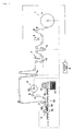
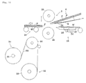
- FIG 1 schematically shows a configuration of an optical element laminating system implementing the optical element laminating method according to one embodiment of the present invention.
- the system according to this embodiment is designed to feed a continuous strip of a polarizing film F to a laminating mechanism 5 for laminating a forwardmost one of the polarizing film sheets F to a liquid-crystal panel W in a sequential manner, and convey the liquid-crystal panel W to the laminating mechanism 5 via a first path which is provided separately from a second path through which the strip of the polarizing film F is passed.
- the feed path for the polarizing film F is provided with a film feeding section 1 from which the polarizing film F is unwound and delivered, the polarizing film strip F comprising a protective film P conformably adhered or attached to a first one of the opposite surfaces thereof and a releasable liner S conformably adhered or attached to the other, second surface thereof, an inspection unit 2 for carrying out an appearance inspection for the polarizing film F, a cutting mechanism 3 for cutting the polarizing film F to a given length in a feed direction to form an array of polarizing film sheets F, and a peeling mechanism 4 for peeling off the releasable liner S from a forwardmost one of the polarizing film sheets F while guiding a leading edge of the forwardmost polarizing film sheet F to the laminating mechanism 5, wherein the peeling mechanism 4 is located in a terminal end of the feed path for the polarizing film F.
- a releasable-liner collecting section 6 is associated with the peeling mechanism 4 to wind up and collect the peeled releasable liner S.
- a plurality of guide rollers g and two dancer rollers 7a, 7b are appropriately interposed between respective ones of the above unit/sections/mechanisms.
- the film feeding section 1, the inspection unit 2, the cutting mechanism 3, the peeling mechanism 4, and the laminating mechanism 5 correspond to, but are not limited to, the optical element feeding means, the inspection means, the cutting means, the peeling means, and the laminating means, respectively.
- the film feeding section 1 is loaded with a roll a continuous strip of a polarization film F prepared by longitudinally slitting a wider strip of polarization film F derived from a stock roll 8 into strips of a given width, the slit strip being wound into a roll.
- the inspection unit 2 is designed to detect defects in the polarizing film F of the strip and foreign substances adhered to the surface of or existing in the polarizing film F, and in this embodiment, a CCD camera as an optical system is employed as the inspection unit 2.
- the CCD camera is disposed directly above the polarizing film strip F to image a portion of the polarizing film strip F passing therebeneath, continuously or intermittently.
- a result of the imaging is converted to a digital signal, and the digital signal is sent to a control unit 9 which will be described in detail later.
- a processing section built in the control unit 9 is operable to perform a matching processing using a reference image acquired from a reference sample identical to an inspection target to detect crack/chip of the polarizing film strip F and attachment of foreign debris.
- the cutting mechanism 3 comprises a holding table 10 for holding a portion of the polarizing film strip F under a suction pressure applied from a back surface thereof, and a laser unit 11 disposed directly above the portion of the polarizing film strip F.
- the laser unit 11 is adapted to be moved horizontally so as to scan a laser beam in a widthwise direction of the polarizing film strip F to cut the lamination of the polarizing film strip F and the protective film strip P at a given pitch in the feed direction, with the lowermost releasable liner being left intact (this cutting will hereinafter be referred as "half-cutting" when appropriate).
- the laser unit 11 is integrally assembled with an air nozzle 12 for blowing warm air toward a cutting position of the polarizing film strip F, and a smoke collection duct 13 for collecting gas (smoke) generated from the cutting position and carried with a stream of the warm air, in such a manner that the air nozzle 12 and the smoke collection duct 13 are disposed on respective ones of opposite sides of the laser unit 11 in the widthwise direction of the polarizing film strip F and in opposed relation to each other.
- the air nozzle 12 and the smoke collection duct 13 correspond to, but are not limited to, the air-blowing means and the smoke-collecting/removing means, respectively.
- the peeling mechanism 4 is provided at an end with a sharp-pointed knife-edged portion 14 which is adapted to provide a path of an acute angle for the releasable liner S by having the releasable liner S passed around the knife-edged portion 14, so as to peel the releasable liner S from the forwardmost one of the sheets of the polarizing film F while guiding the forwardmost polarizing film sheet F toward the laminating mechanism 5. Subsequently, the peeled apart releasable liner S is taken up by a collection bobbin 14 in the releasable-liner collecting section 6.
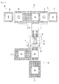
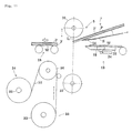
- a plurality of liquid-crystal panels W to be conveyed via the second path are prepared by cutting a wide substrate into sheet-shaped pieces each having a given size, and loaded and stored as a stack in a liquid-crystal panel supply magazine 16 provided in a liquid-crystal panel supply section 17.
- a dummy-substrate supply section 20 is provided in opposed relation to the liquid-crystal panel supply magazine 16 across a panel transport apparatus 18 for receiving and transporting the liquid-crystal panels W, wherein a plurality of dummy substrates DW are loaded and stored as a stack in a dummy-substrate supply magazine 19 provided in the dummy-substrate supply section 20.
- Two vacuum suction-type pickup units 21 are disposed above the liquid-crystal panel supply section 17 and the dummy-substrate supply section 20, respectively, and each of the pickup units 21 is movable in a vertical direction and capable of reciprocating movement in a horizontal direction.
- Each of the pickup units 21 is adapted to hold under suction pressure the liquid-crystal panels W (dummy substrates DW) stored as a stack in the supply magazine 16 (19), one-by-one from the uppermost one.
- the pickup unit 21 in the liquid-crystal panel supply section 17 is adapted to be moved upwardly and then forwardly while holding under suction pressure the liquid-crystal panel W, so as to transfer the liquid-crystal panel W to the panel transport apparatus 18 at a given position between the laminating mechanism 5 and the liquid-crystal panel supply section 17.
- the liquid-crystal panel supply magazine 16 is adapted to be controllably moved upwardly in conjunction with the unloading of the liquid-crystal panel W.
- the pickup unit 21 in the dummy-substrate supply section 20 is adapted to be moved upwardly and then forwardly while holding under suction pressure the dummy substrate DW, so as to transfer the dummy substrate DW to the panel transport apparatus 18 at a given position between the laminating mechanism 5 and the dummy-substrate supply section 20.
- the dummy-substrate supply magazine 20 is adapted to be controllably moved upwardly in conjunction with the unloading of the dummy substrate DW.
- the panel transport apparatus 18 is designed to provide an upstream transport path for transporting the liquid-crystal panels W or the dummy substrates DW to the laminating mechanism 5, and a downstream transport path located downstream of the laminating mechanism 5 to convey the liquid-crystal panels W and the dummy substrate DW each subjected to a laminating operation.
- the upstream transport path is disposed beneath and in overlapped relation with a part of the feed path for feeding the polarizing films F half-cut by the cutting mechanism 3 to the laminating mechanism 5.
- the downstream transport path is divided into two sub-paths to separate the liquid-crystal panel W and the dummy substrate DW from each other.
- the panel transport apparatus 18 is formed as a roller conveyer in both the upstream and downstream transport paths.
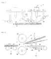
- the feed device 22 is adapted to draw the liquid crystal panel W under a suction pressure and hold it with an appropriate suction force when a liquid crystal panel W is placed on its upper surface, by means of a sucking mechanism 23 through a rectangular opening formed in a central region of the feed plate 22, the sucking mechanism 23 being slidable forwardly and backwardly in a transport direction of the liquid-crystal panels W.
- a cylinder 24 connected to a lower portion of the sucking mechanism 23 is activated to slidingly move the sucking mechanism 23 by a given stroke according to an extending or retracting movement thereof, so that the liquid-crystal panel W (dummy substrate DW) is fed forwardly along the upper surface of the support plate 22.
- the liquid-crystal panel W can be moved forwardly beyond a forward edge of the knife-edged portion 14 and fed to a laminating position.
- the support plate 22 is fixedly installed such that its upper surface is located at a height position higher than an uppermost portion of an after-mentioned first guide roller 25 of the laminating mechanism 5 by an appropriate distance.
- the stroke of the cylinder 24 for slidingly moving the sucking mechanism 23 to feed the liquid-crystal panel W (dummy substrate DW) to the laminating position, and the height position of the upper surface of the feed plate 22, are appropriately determined depending on a size (including a thickness dimension), shape and material of the liquid-crystal panel W.
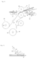
- the laminating mechanism 5 comprises a guide roller 25 and a laminating roller 26.
- the guide roller 25 is comprised of a motor-driven rubber roller
- the laminating roller 26 comprised of a motor-driven metal roller is disposed immediately above the guide roller 25 for movement in the upward and downward directions, whereby, when the feed plate 22 is advanced to feed the liquid-crystal panel W to the laminating position, the laminating roller 26 is moved upwardly to a position higher than the upper surface of the feed plate 22 so as to provide an increased inter-roller gap.
- each of the guide roller 25 and the laminating roller 26 may be comprised of a rubber roller or may be comprised of a metal roller.
- the control unit 9 is provided as a means to generally control a drive mechanism of the system according to this embodiment. Details of the control will be specifically described later in connection with a description about an operation of the system according to this embodiment.
- the structure and function of each of the major components of the optical element laminating system according to this embodiment are just like those described above. The following description will be made about a process of laminating each of the polarizing films F to a respective one of the liquid-crystal panels W, using the above system, with reference to FIGS. 1 to 7 .
- the polarizing film F in the form of a continuous strip is fed out from the stock roll 8 loaded in the film feeding section 1, and fed to the inspection section 2 by being guided with a guide roll g.
- the inspection section 2 an image of the polarizing film strip F is taken and digitized image data is sent to the control unit 9.
- the control unit 9 functions to check the presence or absence of a defect or adhered foreign substance in the polarizing film strip F, based on a matching processing using the received image data and pre-acquired reference image data. After completion of the inspection, the polarizing film strip F is fed to the cutting mechanism 3 via the dancing roller 7a.
- the delivered polarizing film F is held by the holding table 10 under a suction applied from a back surface of the table 10.
- the control unit 9 controls the upstream dancer roller 7a to adequately maintain an operation of feeding the polarizing film strip F from the film feeding section 1.
- the laser unit 11 is moved horizontally in a widthwise direction of the polarizing film strip F to cut the lamination of the polarizing film strip F and the protective film strip P, with the lowermost releasable liner being left intact.
- warm air is blown from the air nozzle 12 toward the cutting position of the lamination of the polarizing film strip F and the protective film strip P, and gas generated from the cutting position is collected and removed through the smoke collection duct 13.
- the holding effort by the holding table 10 is temporarily released to allow the polarizing film strip F to be fed in the feed direction by a given distance, and then the polarizing film strip F is held again under a suction by the holding table 10. Then, the laser unit 11 performs a half-cutting operation for forming a trailing edge of the one polarizing film sheet F.
- the polarizing film F is cut to a size equal to or less than that of the liquid-crystal panel W to which the polarizing film F is to be laminated, the cut sheet of the polarizing film being held adhered to the strip-shaped releasable liner S and feed to the peeling mechanism 4 by being guided by the guide rollers g and according to a movement of the dancer roller 7b.
- the pickup unit 21 picks up an uppermost one of the liquid-crystal panels W from the liquid-crystal panel supply magazine 16 and transfers it to the panel transport apparatus 18.
- the liquid-crystal panel W is then conveyed by means of a conveyor to the laminating mechanism 5.
- the liquid-crystal panel W is transferred to the feed plate 22, and held under a suction pressure applied by the sucking mechanism 23 from the back surface thereof approximately at the same timing of the transfer operation.
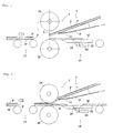
- the control unit 9 controls the operation of the cylinder 24 to feed the liquid-crystal panel W from the feed plate 22 to the guide roller 25, in a manner synchronized with the operation of feeding the leading edge of the forwardmost polarizing film F toward the gap between the laminating roller 26 in the retracted position and the first guide roller 25 in a fixed position, while reversing the feed direction of the releasable liner S along the knife-edged portion 14 of the peeling mechanism 4 to peel the releasable liner S off the forwardmost polarizing film sheet F.
- the laminating roller 26 is moved upwardly to a position apart from the guide roller 25 by a given distance to increase the inter-roll gap, as mentioned above.
- the control unit 9 controls the laminating mechanism 5 to move the laminating roller 26 toward the guide roller 25 by a given distance so as to press the forward portion of the forwardmost polarizing film F against the liquid-crystal panel W to allow the forwardmost polarizing film F to be laminated to the liquid-crystal panel W, as shown in FIG 6 .
- the forwardmost polarizing film F is likely to be bendingly deformed in a chevron shape, due to a residual stress accumulated during the attachment of the releasable liner S and the protective film strip P and a peeling stress caused during the peeling of the releasable liner S.
- the forwardmost polarizing film F is correctively returned to its original flat shape while being pressed by the laminating roller 26, and pressed against and in parallel relation to an upper surface of the liquid-crystal panel W.
- the polarizing film F detached from the strip-shaped releasable liner S will be continuously fed between the first guide roller 25 and the laminating roller 26 and laminated to the upper surface of the liquid-crystal panel W.
- the control unit 9 also controls the dancer roller 7b in synchronization with the laminating roller 26, the wind-up operation of the releasable-liner collecting section 6, and an activation and deactivation of the laminating mechanism 5, to allow the above series of operations to be adequately performed.
- the liquid-crystal panel W with the polarizing film F laminated thereto is conveyed to a next station via the downstream transport path of the panel transport apparatus 18. In this manner, one cycle of laminating operation for the polarizing film F having no defect is completed.
- a processing section built in the control unit 9 calculates a position coordinate of the defect based on image data acquired by the inspection unit 2, and controls to allow a defective polarizing film F including this defect to be laminated to the dummy substrate DW instead of being laminated to the liquid-crystal panel W, based on the calculated position coordinate.
- a distance between a position of the polarizing film strip F at a timing of the detection of a defect, such as crack/chip, and the laminating mechanism 5, is known.
- the control unit 9 activates an encoder to count a rotational amount of a drive mechanism for feeding the polarizing film strip (polarizing films) F.
- control unit 9 calculates a timing when the defective polarizing film F reaches the laminating mechanism 5, and then operates to allow the dummy substrate DW to be transferred from the dummy-substrate supply section 20 to the panel transport apparatus 18, based on the calculation result. Then, when each of the defective polarizing film F and the dummy substrate DW reaches the laminating mechanism 5, a laminating operation is performed in the same manner as that for the non-defective polarizing film F, and the dummy substrate DW with the defective polarizing film F laminated thereto is conveyed via the downstream path in the panel transport apparatus 18.
- the dummy substrate DW with the defective polarizing film F, laminated thereto is conveyed in a direction different from that for the non-defective polarizing film F at a branched position of the downstream path, and collected. In this manner, one cycle of a laminating operation using the dummy substrate DW is completed.
- the following process may be performed.
- the polarizing film sheet F to be laminated to the liquid-crystal panel W has a width Y of 476 mm and a length H of 836 mm
- the position coordinate of the defect is calculated based on image data acquired by the inspection unit 2, and a trailing cut position is determined for defining a trailing edge of a defective polarizing film sheet to be formed at a position apart from the calculated position of the defect by a given length (in this example, 100 mm).
- an inspection is conducted to determine if there is no defect within the distance (836 mm) from the trailing cut position for ensuring a non-defective sheet size of the polarizing film F.
- a further half-cut position X3 is determined if it is possible to ensure a length of a non-defective sheet of the polarizing film F.
- the area between the position X3 to the next cut position X7 is divided into a plurality of areas so that each divided area is within the size of the dummy substrate DW.
- the lamination of the protective film strip P and the polarizing film strip F is half-cut by the laser unit 11 while leaving the releasable liner S intact, so that it is made possible to deliver sequentially arranged sheets of polarizing films F each having a size equal to or less than that of the liquid-crystal panel W, on the strip-shaped releasable liner S.
- the releasable liner S is peeled off from a forwardmost one of the polarizing film sheet F by reversing the feed direction of the releasable liner S along the knife-edged portion 14 of the peeling mechanism 4, while allowing the forwardmost polarizing film F to be fed to the laminating mechanism 5 and laminated to the liquid-crystal panel W.
- the array of polarizing film sheets F each having approximately the same shape of that of the liquid-crystal panel can be fed substantially in the form of a strip and automatically laminated to respective ones of the liquid-crystal panels. Further, during this operation, the opposite surfaces of the polarizing film sheets F are covered respectively by the releasable liner S and the protective film strip, until the polarizing film sheet F is laminated to the corresponding liquid-crystal panel W, so that it is made possible to prevent contamination, such as dust, from attaching to the top and bottom surfaces of the polarizing film strip F. In addition, even after the laminating operation, the protective film P is still adhered to the surface of the polarizing film F to prevent dust from being adhered thereto.
- the mechanism for blowing warm air against a cutting position during the half-cutting of the polarizing film strip F by the laser unit 11 and collecting/removing generated gas in the system according to the above embodiment will be more specifically described based on the following examples.
- Example 1 warm air at 60°C was blown from the air nozzle 12 against the cutting position of the polarizing film strip F while collecting and removing generated gas through the smoke collection dust 13.
- Example 2 the half-cutting operation based on the laser unit 11 was performed at an ambient air temperature without air-blowing and without collection/removal of generated gas.
- Example 3 the half-cutting operation based on the laser unit 11 was performed at an ambient air temperature with only collecting and removing generated gas.
- Example 4 under a condition that a room temperature is maintained at constant value of 25°C, warm air at the same temperature as the room temperature, i.e., 25°C, was blown against the cutting position while collecting and removing generated gas.
- Example 1 As a result, as shown in Table 1, in Example 1, adherence of foreign substances was not observed in the cutting position and its surrounding region. In contrast, in Examples 2 to 4, adherence of foreign substances in a strip pattern with a certain width was observed around and on both sides of the cutting position. The widths of the adhered foreign substances in Example 2, Example 3 and Example 4 were 9 mm, 8 mm and 2 mm, respectively. That is, in either case devoid of blowing of warm air, adherence of foreign substances was observed on both sides of the cutting position.
- the above embodiment of the present invention may be modified as follows.
- the inspection unit 2 in the above embodiment may be designed such that a light source and a light-receiving element or a line sensor are disposed on respective ones of upper and lower sides of the polarizing film strip and in opposed relation to each other, to detect crack/chip of the polarizing film strip and attachment of foreign substance thereon, based on a change in intensity of light transmitted through the polarizing film strip being passing therebetween.
- the inspection unit 2 having an optical system described above to detect defects such as loss of specific optical feature with a high accuracy, by eliminating any adverse effect caused by for example variations in orientation of the releasable liner S and influence of reflected light.
- a laminate film has been prepared using films of T-VEGQ1724DU ARC15T-AC manufactured by Nitto Denko Corporation for the protective film strip P, the polarizing film strip F and the releasable liner S.
- This laminate film had a width of 1500 mm.
- the feed speed of the polarizing film strip F was set at 50 m/min.
- inspection has been conducted to detect respectively adherence of foreign substances on the surface of the polarizing film strip F or other film, and a knick which is a defect of a particular shape causing an optical distortion and having a dent-like configuration created by foreign debris being caught in or on the film during manufacturing process.
- the inspection has been conducted to detect a defect having a size of 100 ⁇ m or greater in a unit area of 560 mm ⁇ 600 mm.
- the defects were detected at 380 locations in the case of the polarizing film strip F having the releasable liner strip S removed, and detected at 354 locations in the case of the polarizing film strip F with the releasable liner strip S attached thereto.
- FIG 9 shows the above results. It should be noted that, a detection accuracy of foreign substances and the knick could be improved through the inspection of the polarizing film strip F after temporarily removing the releasable liner strip S therefrom. This makes it possible to laminate a high-quality polarizing film F to a liquid-crystal panel W.
- the defective polarizing film strip F is collected by being laminated on the dummy substrate DW, however, in an alternative way, the defective polarizing film may be collected by being laminated on a strip-shaped member.
- the first guide roller 25 in the laminating mechanism 5 may be designed to be selectively moved in a vertical direction so as to increase a space for the laminating operation.
- a second guide roller 36 may be disposed obliquely below the first guide roller 25 for bringing a strip-shaped member S3 unrolled from a stock roll 33 of the member S3 and passed around a collection bobbin 35 in a collecting section 34 to a position opposed to the laminating roller 26 for laminating the defective polarizing film F to the strip-shaped member S3.
- the first guide roller 25 is moved downwardly to increase the space below the laminating roller 26, as shown in FIG 11
- the second guide roller 36 is moved upwardly to the laminating position where the first guide roller 25 has been previously located, as shown in FIG 12 .
- the laminating roller 26 is moved downwardly to press and laminate the defective polarizing film F to the releasable member S3, as shown in FIG 13 .
- the releasable-liner collecting section 6 and the strip-shaped member collecting section 34 are operable to wind and collect the releasable liner S and the strip-shaped member S3, respectively.
- the second guide roller 36 is moved downwardly to return to a retracted position, and the first guide roller 25 is moved upwardly to return to the laminating position.
- the present invention is not limited to such a mechanism, but any other suitable mechanism may be adopted as long as it is capable of accurately feeding the liquid-crystal panel W to the first guide roller 25.
- the mechanism may be designed to convey the liquid-crystal panel W directly from the roller conveyer toward the first guide roller 25.
- the optical axis of the laser beam when a laser beam is moved to scan in the widthwise direction of the polarizing film strip F, the optical axis of the laser beam is set to be perpendicular to the cutting position, however, in an alternative arrangement, the optical axis of the laser beam may be set as follows.
- the laser unit 11 may be installed in an inclined posture in such a manner that an optical axis R of the laser beam emitted from the unit is inclined to extend from the forward side of the transverse scanning line of the laser beam as seen in the longitudinal traveling direction of the polarizing film F toward the cutting position.
- an installation angle of the laser unit 11 is set such that an angle ⁇ between the optical axis R of the laser beam and a reference axis perpendicular to the cutting position is in the range of 10 to 45 degrees.
- the installation angle ⁇ is more preferably set in the range of 20 to 45 degrees, particularly preferably in the range of 30 to 45 degrees.
- the installation angle ⁇ is less than 10 degrees, for example zero degree as shown in FIG 16 , smoke generated during the cutting operation flows backwardly with respect to the scanning line of the laser beam in the traveling direction of the polarizing film F along the surface of the protective film strip P, so that the smoke is liable to cover the surface of the protective film strip P to cause adherence of foreign substances, resulting in a higher degree of contamination.
- the laser unit 11 is installed in an inclined posture to emit the laser beam in such a manner that the optical axis R of the laser beam is inclined to extend from the rearward side of the laser scanning line as seen in the traveling direction toward the cutting position, smoke generated during the cutting operation flows along the surface of the protective film strip P, in the same manner as that in FIG 16 .
- the width (as measured in the traveling direction) of the area where foreign substances are adhered around the cutting position was 0.9 mm in the Example 6 and it has been observed that the width becomes smaller as the angle ⁇ is increased in the order from the Example 7 to the Example 11. Particularly, in the Examples 10 and 11, no adherence of foreign substances was observed. In contrast, as seen in Table 2, the width of the area having foreign substances adhered thereon in the Example 5 is 1.65 mm, and it has been recognized that the degree of contamination is almost two times greater than that in the other Examples 6 to 11.
- the adherence of foreign substances at the cutting position and the surrounding region due to smoke generated during the cutting operation can be suppressed by installing the laser unit in an inclined posture in such a manner that the optical axis R of the laser beam is inclined to extend from a forward side in the traveling direction of the film relative to and toward the cutting position.
- a carbon dioxide laser beam any other suitable laser beam may be appropriately adopted depending on an intended purpose.
- a YAG laser beam or a UV laser beam may be used.
- the present invention is suitable for use in automatically laminating an optical element cut to a given length, to a sheet-shaped body.
Priority Applications (2)
| Application Number | Priority Date | Filing Date | Title |
|---|---|---|---|
| PL07829703T PL2093041T3 (pl) | 2006-10-17 | 2007-10-12 | Sposób przyklejania elementu optycznego i urządzenie wykorzystujące ten sposób |
| EP11182532A EP2437049A1 (fr) | 2006-10-17 | 2007-10-12 | Procédé et système de stratification d'éléments optiques |
Applications Claiming Priority (4)
| Application Number | Priority Date | Filing Date | Title |
|---|---|---|---|
| JP2006282378 | 2006-10-17 | ||
| JP2007211001 | 2007-08-13 | ||
| JP2007266200A JP4361103B2 (ja) | 2006-10-17 | 2007-10-12 | 光学部材貼合せ方法およびそれを用いた装置 |
| PCT/JP2007/069967 WO2008047712A1 (fr) | 2006-10-17 | 2007-10-12 | Procédé d'adhésion d'élément optique et appareil utilisant le procédé |
Related Child Applications (1)
| Application Number | Title | Priority Date | Filing Date |
|---|---|---|---|
| EP11182532.9 Division-Into | 2011-09-23 |
Publications (3)
| Publication Number | Publication Date |
|---|---|
| EP2093041A1 true EP2093041A1 (fr) | 2009-08-26 |
| EP2093041A4 EP2093041A4 (fr) | 2011-06-08 |
| EP2093041B1 EP2093041B1 (fr) | 2013-02-20 |
Family
ID=40556587
Family Applications (2)
| Application Number | Title | Priority Date | Filing Date |
|---|---|---|---|
| EP07829703A Expired - Fee Related EP2093041B1 (fr) | 2006-10-17 | 2007-10-12 | Procédé d'adhésion d'élément optique et appareil utilisant le procédé |
| EP11182532A Ceased EP2437049A1 (fr) | 2006-10-17 | 2007-10-12 | Procédé et système de stratification d'éléments optiques |
Family Applications After (1)
| Application Number | Title | Priority Date | Filing Date |
|---|---|---|---|
| EP11182532A Ceased EP2437049A1 (fr) | 2006-10-17 | 2007-10-12 | Procédé et système de stratification d'éléments optiques |
Country Status (8)
| Country | Link |
|---|---|
| US (2) | US7922843B2 (fr) |
| EP (2) | EP2093041B1 (fr) |
| JP (1) | JP4361103B2 (fr) |
| KR (1) | KR101010990B1 (fr) |
| CN (2) | CN102837437B (fr) |
| PL (1) | PL2093041T3 (fr) |
| TW (1) | TWI332434B (fr) |
| WO (1) | WO2008047712A1 (fr) |
Cited By (9)
| Publication number | Priority date | Publication date | Assignee | Title |
|---|---|---|---|---|
| EP2267516A1 (fr) * | 2008-04-15 | 2010-12-29 | Nitto Denko Corporation | Rouleau stratifié de film optique, et son procédé et appareil de production |
| EP2246835A4 (fr) * | 2008-04-08 | 2011-03-16 | Nitto Denko Corp | Système de fabrication d un dispositif d affichage optique, procédé de fabrication d un dispositif d affichage optique, dispositif d enlèvement et procédé d enlèvement |
| EP2312381A1 (fr) * | 2009-10-13 | 2011-04-20 | Nitto Denko Corporation | Rouleau d'un film optique stratifié pourvu de fentes prédéfinies, et procédé et appareil pour la fabrication dudit rouleau |
| EP2315071A1 (fr) * | 2009-10-13 | 2011-04-27 | Nitto Denko Corporation | Procédé et système pour fabriquer de manière continue un élément d'affichage à cristaux liquides |
| EP2325007A1 (fr) * | 2009-10-13 | 2011-05-25 | Nitto Denko Corporation | Procédé et système pour fabriquer de manière continue un élément d'affichage à cristaux liquides |
| EP2426526A1 (fr) * | 2010-09-03 | 2012-03-07 | Nitto Denko Corporation | Procédé et appareil de stratification séquentielle d'un film optique, incluant un film de polarisation, sur un panneau en forme rectangulaire |
| US20120097325A1 (en) * | 2010-10-21 | 2012-04-26 | Nitto Denko Corporation | System and method for continuously manufacturing liquid crystal display device |
| EP2476553A1 (fr) * | 2011-01-14 | 2012-07-18 | Nitto Denko Corporation | Procédé pour fabriquer en continu un dispositif d'affichage à cristaux liquides |
| CN103153526A (zh) * | 2010-10-06 | 2013-06-12 | 住友化学株式会社 | 激光切割装置及具有该装置的切条机 |
Families Citing this family (105)
| Publication number | Priority date | Publication date | Assignee | Title |
|---|---|---|---|---|
| PL2093041T3 (pl) | 2006-10-17 | 2013-08-30 | Nitto Denko Corp | Sposób przyklejania elementu optycznego i urządzenie wykorzystujące ten sposób |
| WO2009025210A1 (fr) * | 2007-08-23 | 2009-02-26 | Nitto Denko Corporation | Procédé et appareil pour inspecter un défaut d'un film stratifié |
| JP2009069142A (ja) | 2007-08-23 | 2009-04-02 | Nitto Denko Corp | 積層フィルムの欠陥検査方法およびその装置 |
| JP2009157361A (ja) * | 2007-12-06 | 2009-07-16 | Nitto Denko Corp | 偏光板及び画像表示装置 |
| WO2009072470A1 (fr) * | 2007-12-06 | 2009-06-11 | Nitto Denko Corporation | Procédé de fabrication d'un dispositif d'affichage d'images |
| JP5261681B2 (ja) * | 2008-07-01 | 2013-08-14 | 日東電工株式会社 | 光学フィルムを有する積層フィルムの切断方法および光学表示装置の製造方法 |
| JP2010053310A (ja) * | 2008-08-29 | 2010-03-11 | Nitto Denko Corp | レーザーハーフカット加工品の製造方法 |
| TWI406053B (zh) * | 2008-12-25 | 2013-08-21 | Nitto Denko Corp | A layering method of polarizing plate and a laminated system of polarizing plate |
| KR101179071B1 (ko) | 2009-03-10 | 2012-09-03 | 주식회사 엘지화학 | 사각형 단위체의 제조방법 |
| JP4673414B2 (ja) * | 2009-03-18 | 2011-04-20 | 日東電工株式会社 | 液晶表示素子の製造方法 |
| JP2010262265A (ja) | 2009-04-10 | 2010-11-18 | Nitto Denko Corp | 光学フィルムロール原反、およびそれを用いた画像表示装置の製造方法 |
| CN102067021B (zh) * | 2009-05-15 | 2014-03-26 | 日东电工株式会社 | 光学显示装置的制造系统及制造方法、辊状卷料组件及其制造方法 |
| JP2011006648A (ja) * | 2009-06-29 | 2011-01-13 | Nitto Denko Corp | 光学シート部材の巻回体および液晶表示装置の連続製造方法 |
| JP2011008195A (ja) * | 2009-06-29 | 2011-01-13 | Nitto Denko Corp | 光学シート部材の巻回体および液晶表示装置の連続製造方法 |
| WO2011016572A1 (fr) * | 2009-08-06 | 2011-02-10 | 住友化学株式会社 | Procédé de fabrication de plaques polarisantes |
| JP4503692B1 (ja) | 2009-10-13 | 2010-07-14 | 日東電工株式会社 | 液晶表示素子を連続製造する装置において用いられる情報格納読出演算システム及び情報格納読出演算システムの製造方法 |
| JP4503690B1 (ja) | 2009-10-13 | 2010-07-14 | 日東電工株式会社 | 液晶表示素子を連続製造する装置に用いられる情報格納読出システム、及び、前記情報格納読出システムを製造する方法及び装置 |
| KR101255497B1 (ko) * | 2009-12-09 | 2013-04-16 | 수미토모 케미칼 컴퍼니 리미티드 | 광학표시장치의 제조시스템 |
| KR101704556B1 (ko) * | 2010-02-12 | 2017-02-08 | 동우 화인켐 주식회사 | 편광판의 커팅 장치 및 방법 |
| JP4751997B1 (ja) * | 2010-02-17 | 2011-08-17 | 住友化学株式会社 | 偏光フィルムの貼合装置およびこれを備える液晶表示装置の製造システム |
| WO2011105273A1 (fr) * | 2010-02-24 | 2011-09-01 | 住友化学株式会社 | Procédé de fabrication d'un dispositif d'affichage à cristaux liquides |
| JP4977257B2 (ja) * | 2010-06-24 | 2012-07-18 | 日東電工株式会社 | 液晶パネルの製造方法及び製造システム |
| JP5481300B2 (ja) * | 2010-07-29 | 2014-04-23 | 住友化学株式会社 | 偏光板切断方法および当該方法によって切断された偏光板 |
| JP4972198B2 (ja) | 2010-08-27 | 2012-07-11 | 日東電工株式会社 | 光学機能フィルム連続ロール、およびそれを用いた液晶表示素子の製造方法、ならびに光学機能フィルム貼り合せ装置 |
| JP4972197B2 (ja) | 2010-08-27 | 2012-07-11 | 日東電工株式会社 | 光学機能フィルム連続ロール、およびそれを用いた液晶表示素子の製造方法、ならびに光学機能フィルム貼り合せ装置 |
| JP5167319B2 (ja) | 2010-09-01 | 2013-03-21 | 日東電工株式会社 | 光学機能フィルム、及びこれを用いた液晶表示装置の製造方法 |
| JP5478553B2 (ja) | 2010-09-03 | 2014-04-23 | 日東電工株式会社 | 連続ウェブ状光学フィルム積層体ロール及びその製造方法 |
| JP5511730B2 (ja) | 2010-09-03 | 2014-06-04 | 日東電工株式会社 | 光学的パネル組立体の連続的製造方法及び装置 |
| JP5474869B2 (ja) * | 2010-09-03 | 2014-04-16 | 日東電工株式会社 | 偏光膜を有する積層体ストリップロールの製造方法 |
| JP5704173B2 (ja) * | 2010-09-17 | 2015-04-22 | コニカミノルタ株式会社 | 光学表示装置の製造システム及び製造方法 |
| JP4689763B1 (ja) * | 2010-09-29 | 2011-05-25 | 日東電工株式会社 | 液晶表示素子の連続製造システムおよび液晶表示素子の連続製造方法 |
| JP5197708B2 (ja) | 2010-10-13 | 2013-05-15 | 日東電工株式会社 | 液晶表示素子の連続製造方法および液晶表示素子の連続製造システム |
| JP2012093985A (ja) | 2010-10-27 | 2012-05-17 | Nitto Denko Corp | タッチ入力機能を有する表示パネル装置と該表示パネル装置のための光学ユニット、並びにその製造方法 |
| JP4878070B2 (ja) * | 2010-10-29 | 2012-02-15 | 日東電工株式会社 | 液晶表示素子の製造方法 |
| JP5243514B2 (ja) | 2010-11-12 | 2013-07-24 | 日東電工株式会社 | 液晶表示装置の製造方法 |
| JP5140788B2 (ja) * | 2010-11-22 | 2013-02-13 | 日東電工株式会社 | 液晶表示素子の連続製造システムおよび液晶表示素子の連続製造方法 |
| JP5461371B2 (ja) * | 2010-11-25 | 2014-04-02 | 日東電工株式会社 | 液晶表示素子の製造方法および液晶表示素子の製造システム |
| KR20120070339A (ko) * | 2010-12-21 | 2012-06-29 | 제일모직주식회사 | 액정 디스플레이 및 편광판 제조방법 |
| JP4844857B1 (ja) * | 2011-02-23 | 2011-12-28 | 住友化学株式会社 | 回収装置、貼合システム及び回収方法 |
| JP5667522B2 (ja) | 2011-06-09 | 2015-02-12 | 住友化学株式会社 | 光学表示装置の製造システムおよび光学表示装置の製造方法 |
| JP5068876B1 (ja) * | 2011-06-10 | 2012-11-07 | 日東電工株式会社 | 液晶表示素子の連続製造方法及び装置 |
| KR101860597B1 (ko) * | 2011-06-29 | 2018-05-23 | 수미토모 케미칼 컴퍼니 리미티드 | 나이프 엣지 및 이것을 포함하는 액정 표시 장치의 제조 시스템 |
| US8853591B2 (en) * | 2011-07-14 | 2014-10-07 | Cheng Uei Precision Industry Co., Ltd. | Surface treatment equipment including a laser engraving system for treatment of a strip |
| JP5572193B2 (ja) * | 2011-09-21 | 2014-08-13 | 住友化学株式会社 | 偏光板の製造方法 |
| JP2013128966A (ja) * | 2011-12-22 | 2013-07-04 | Sumitomo Chemical Co Ltd | レーザー光照射装置、フィルム切断装置、レーザー光照射方法及びフィルム切断方法 |
| CN104115209B (zh) * | 2012-02-29 | 2018-04-24 | 住友化学株式会社 | 光学显示设备的生产系统以及光学显示设备的生产方法 |
| WO2013129256A1 (fr) * | 2012-02-29 | 2013-09-06 | 住友化学株式会社 | Système de fabrication de dispositif d'affichage optique et procédé de fabrication de dispositif d'affichage optique |
| KR101436806B1 (ko) | 2012-03-08 | 2014-09-03 | 엘지디스플레이 주식회사 | 디스플레이 장치 및 그의 제조 방법 |
| JP5307947B1 (ja) | 2012-03-30 | 2013-10-02 | 日東電工株式会社 | 液晶表示装置の製造方法 |
| JPWO2013151035A1 (ja) * | 2012-04-03 | 2015-12-17 | 住友化学株式会社 | 光学表示デバイスの生産システム |
| JP6101431B2 (ja) * | 2012-04-16 | 2017-03-22 | 日東電工株式会社 | 光学表示パネルの連続製造方法および光学表示パネルの連続製造システム |
| JP5828961B2 (ja) * | 2012-08-08 | 2015-12-09 | 住友化学株式会社 | 光学表示デバイスの生産方法および光学表示デバイスの生産システム |
| CN104541318B (zh) * | 2012-08-08 | 2016-11-23 | 住友化学株式会社 | 光学显示器件的生产系统以及光学显示器件的生产方法 |
| JP5946362B2 (ja) | 2012-08-10 | 2016-07-06 | 日東電工株式会社 | 光学表示パネルの製造方法および光学表示パネルの製造システム |
| CN104583847B (zh) * | 2012-09-07 | 2018-04-13 | 住友化学株式会社 | 光学构件贴合体的制造装置 |
| JP5452761B1 (ja) | 2012-10-10 | 2014-03-26 | 日東電工株式会社 | 光学的表示装置を製造する方法及び装置 |
| JP5452762B1 (ja) | 2012-10-10 | 2014-03-26 | 日東電工株式会社 | 光学表示装置を製造する方法及び装置 |
| JP5782010B2 (ja) * | 2012-11-09 | 2015-09-24 | 日東電工株式会社 | 光学表示パネルの連続製造方法および光学表示パネルの連続製造システム |
| JP5458212B1 (ja) | 2012-11-19 | 2014-04-02 | 日東電工株式会社 | 光学的表示装置を製造する方法及び装置 |
| JP5458211B1 (ja) * | 2012-11-19 | 2014-04-02 | 日東電工株式会社 | 光学的表示装置を製造する方法及び装置 |
| JP2014186287A (ja) * | 2013-02-20 | 2014-10-02 | Sumitomo Chemical Co Ltd | 光学表示デバイスの生産システム及び生産方法 |
| JP6120161B2 (ja) * | 2013-04-08 | 2017-04-26 | 住友化学株式会社 | レーザー加工装置及び光学表示デバイスの生産システム |
| CN103264503B (zh) * | 2013-06-03 | 2015-12-09 | 深圳市发得快科技有限公司 | 一种发泡塑胶自动化粘接设备 |
| JP5616494B1 (ja) * | 2013-07-04 | 2014-10-29 | 日東電工株式会社 | 積層体基板の形成方法および装置 |
| JP5452760B1 (ja) * | 2013-09-25 | 2014-03-26 | 日東電工株式会社 | 光学的表示装置を製造する方法および装置 |
| KR102128396B1 (ko) * | 2013-10-22 | 2020-07-01 | 삼성디스플레이 주식회사 | 필름 박리 장치 |
| JP6247899B2 (ja) * | 2013-11-01 | 2017-12-13 | 花王株式会社 | シート融着体の製造装置及び製造方法 |
| JP2015108664A (ja) * | 2013-12-03 | 2015-06-11 | 住友化学株式会社 | 光学部材貼合体の製造装置 |
| WO2015105240A1 (fr) * | 2014-01-08 | 2015-07-16 | 주식회사 엘지화학 | Système pour stratifier un film optique et procédé de fabrication d'une unité d'affichage l'utilisant |
| US9694571B2 (en) | 2014-01-08 | 2017-07-04 | Lg Chem, Ltd. | System for laminating optical film and method for manufacturing display unit using the same |
| WO2015105242A1 (fr) * | 2014-01-08 | 2015-07-16 | 주식회사 엘지화학 | Système pour stratifier un film optique et procédé de fabrication d'unité d'affichage l'utilisant |
| KR101540431B1 (ko) * | 2014-01-08 | 2015-07-30 | 주식회사 엘지화학 | 광학 필름 라미네이팅 시스템 및 이를 이용한 디스플레이 유닛 제조방법 |
| US9682543B2 (en) | 2014-01-08 | 2017-06-20 | Lg Chem, Ltd. | System for laminating optical film and method for manufacturing display unit using the same |
| US9498942B2 (en) | 2014-02-28 | 2016-11-22 | Lg Chem, Ltd. | System for laminating optical film and method for manufacturing display unit using the same |
| KR101495763B1 (ko) * | 2014-02-28 | 2015-02-25 | 주식회사 엘지화학 | 광학 필름 라미네이팅 시스템 및 이를 이용한 디스플레이 유닛 제조방법 |
| JP5711833B2 (ja) * | 2014-03-11 | 2015-05-07 | 日東電工株式会社 | タッチ入力機能を有する表示パネル装置と該表示パネル装置のための光学ユニット、並びにその製造方法 |
| CN105269608A (zh) | 2014-06-24 | 2016-01-27 | 日东电工株式会社 | 层积型光学膜切割装置及层积型光学膜切割方法 |
| JP6401526B2 (ja) * | 2014-07-09 | 2018-10-10 | 住友化学株式会社 | 貼合装置、貼合方法、光学表示デバイスの生産システム及び光学表示デバイスの生産方法 |
| KR101713880B1 (ko) * | 2014-08-14 | 2017-03-22 | 주식회사 엘지화학 | 필름 텐션 조절 시스템 및 이를 포함하는 편광판 제조 시스템 |
| JP6305884B2 (ja) * | 2014-09-09 | 2018-04-04 | 株式会社日立プラントメカニクス | フィルムのラミネート装置及びその動作方法 |
| CN104589776B (zh) * | 2014-12-26 | 2016-11-30 | 东莞市智澳通用机械设备有限公司 | 一种遮光膜供料机构 |
| JP6403159B2 (ja) * | 2015-02-26 | 2018-10-10 | 株式会社日立プラントメカニクス | フィルムの真空ラミネート装置 |
| CN106469767B (zh) * | 2015-08-18 | 2017-12-01 | 江苏诚睿达光电有限公司 | 一种基于串联滚压的有机硅树脂光转换体贴合封装led的装备系统 |
| JP6543152B2 (ja) * | 2015-09-30 | 2019-07-10 | リンテック株式会社 | シート貼付装置および貼付方法並びに接着シート原反 |
| CN105242419A (zh) * | 2015-11-08 | 2016-01-13 | 温州智信机电科技有限公司 | 一种贴片可靠的手机偏光片贴合机 |
| JP6188868B1 (ja) * | 2016-05-26 | 2017-08-30 | 住友化学株式会社 | 偏光板、及び液晶表示装置 |
| KR101674352B1 (ko) * | 2016-05-30 | 2016-11-08 | 주식회사 엘지화학 | 광학 표시 소자의 제조 시스템 및 제조 방법 |
| KR101704973B1 (ko) * | 2016-05-31 | 2017-02-08 | 주식회사 엘지화학 | 디스플레이 유닛 제조 시스템 |
| JP6538014B2 (ja) * | 2016-09-06 | 2019-07-03 | 日東電工株式会社 | 光学的表示ユニットの連続製造装置及び連続製造方法 |
| SE540604C2 (en) * | 2016-12-01 | 2018-10-02 | Stora Enso Oyj | Method and arrangement for laser-based processing of fibrous material |
| JP6870974B2 (ja) * | 2016-12-08 | 2021-05-12 | 株式会社ディスコ | 被加工物の分割方法 |
| TWI685905B (zh) * | 2017-07-12 | 2020-02-21 | 日商新川股份有限公司 | 接合裝置和接合方法 |
| KR102124184B1 (ko) | 2017-09-26 | 2020-06-17 | 주식회사 엘지화학 | 광학필름 부착시스템 |
| JP7028607B2 (ja) * | 2017-11-06 | 2022-03-02 | 株式会社ディスコ | 切削装置 |
| EP3488960B1 (fr) * | 2017-11-23 | 2020-11-25 | Dallan S.p.A. | Appareil de découpe au laser ou au plasma de pièces de matériau laminaire enroulées en bobine |
| US11370212B2 (en) | 2018-02-13 | 2022-06-28 | Lg Chem, Ltd. | System and apparatus for laminating optical film |
| KR101893901B1 (ko) * | 2018-06-01 | 2018-08-31 | 주식회사 에이엘텍 | 알루미늄 박 검품 및 절단 장치와 이의 제어 방법 |
| CN109397673A (zh) * | 2018-10-31 | 2019-03-01 | 江苏赛诺格兰医疗科技有限公司 | 一种esr膜折叠方法 |
| TWI710288B (zh) * | 2020-01-22 | 2020-11-11 | 頎邦科技股份有限公司 | 電路板的散熱片貼合方法及其貼合裝置 |
| KR102121825B1 (ko) * | 2020-02-28 | 2020-06-12 | 주식회사알메탈 | 금속판 보호필름 부착장치 |
| CN111413759A (zh) * | 2020-03-25 | 2020-07-14 | 深圳同兴达科技股份有限公司 | 一种偏光片的制作方法 |
| CN114080149A (zh) * | 2020-08-20 | 2022-02-22 | 三赢科技(深圳)有限公司 | 剥离装置 |
| JP7476141B2 (ja) | 2021-07-05 | 2024-04-30 | 日本ピストンリング株式会社 | ワーク加工装置 |
| CN113547749A (zh) * | 2021-07-26 | 2021-10-26 | 重庆凯丰医疗器械有限公司 | 具有除杂功能的tdp灸疗贴的粉料装填装置 |
| JP7471559B1 (ja) | 2023-06-15 | 2024-04-22 | 株式会社エヌ・シー・ティ | シート真空ラミネート装置 |
Citations (3)
| Publication number | Priority date | Publication date | Assignee | Title |
|---|---|---|---|---|
| DE3232060A1 (de) * | 1981-09-09 | 1983-03-24 | Fis Organisation GmbH, 2000 Hamburg | Verfahren und zwischenprodukt fuer die herstellung eines einstueckigen maschinenlesbaren informationstraegers |
| US5062340A (en) * | 1990-06-21 | 1991-11-05 | Richard Greven | Cutting and positioning apparatus |
| WO2006100818A2 (fr) * | 2005-03-23 | 2006-09-28 | Fujifilm Corporation | Appareil et procede permettant de fabriquer un corps lamine photosensible |
Family Cites Families (23)
| Publication number | Priority date | Publication date | Assignee | Title |
|---|---|---|---|---|
| JPS6054641B2 (ja) | 1979-03-09 | 1985-11-30 | 日東電工株式会社 | 粘着偏光板のセルへの自動的連続貼着方法 |
| JPS5752018A (en) | 1980-08-08 | 1982-03-27 | Sharp Corp | Tacky-polarizing-plate sticking device of automatic tacky-polarizing-plate sticking machine |
| JPS5752017A (en) | 1980-08-08 | 1982-03-27 | Sharp Corp | Tacky-polarizing-plate defective removing device automatic tacky-polarizing-plate sticking machine |
| JPS5752019A (en) | 1980-08-08 | 1982-03-27 | Sharp Corp | Automatic sticking method for tacky polarizing plate |
| JPH07157186A (ja) | 1993-12-08 | 1995-06-20 | Sharp Corp | 連続ラミネート装置 |
| US6592693B1 (en) * | 2000-08-11 | 2003-07-15 | Greydon Wesley Nedblake | Method and apparatus for laser cutting of adhesive-bearing webs separate from liner webs |
| US20030061947A1 (en) * | 2001-10-01 | 2003-04-03 | Hohberger Clive P. | Method and apparatus for associating on demand certain selected media and value-adding elements |
| JP2005037417A (ja) | 2002-06-28 | 2005-02-10 | Fuji Photo Film Co Ltd | 偏光板貼合方法及び装置 |
| JP4376558B2 (ja) | 2002-07-04 | 2009-12-02 | 富士フイルム株式会社 | 偏光板貼合方法及び装置 |
| JP2004338408A (ja) * | 2003-04-24 | 2004-12-02 | Mitsui Chemicals Inc | フィルムのラミネート方法および装置 |
| JP2004345354A (ja) * | 2003-04-24 | 2004-12-09 | Mitsui Chemicals Inc | フィルムのラミネート方法および装置 |
| JP4342829B2 (ja) | 2003-05-01 | 2009-10-14 | 富士フイルム株式会社 | 光学フィルム貼付装置、方法及び基板 |
| JP4346971B2 (ja) | 2003-05-16 | 2009-10-21 | 富士フイルム株式会社 | 偏光板貼合方法及び装置 |
| JP4371709B2 (ja) | 2003-06-05 | 2009-11-25 | 富士フイルム株式会社 | 光学フィルム貼付装置及び方法 |
| JP2005062165A (ja) * | 2003-07-28 | 2005-03-10 | Nitto Denko Corp | シート状製品の検査方法、検査システム、シート状製品、及び、画像表示装置 |
| JP2005114624A (ja) | 2003-10-09 | 2005-04-28 | Nitto Denko Corp | シート状製品の検査方法及びシート状製品の検査システム及びシート状製品及び枚葉物 |
| TWI278386B (en) | 2003-10-17 | 2007-04-11 | Jin Taiwan Entpr Co Ltd | Method of manufacturing light diffusion plate and the light diffusion plate thereof |
| JP4302042B2 (ja) | 2004-03-26 | 2009-07-22 | 富士フイルム株式会社 | フイルム剥離装置 |
| JP4620433B2 (ja) * | 2004-03-26 | 2011-01-26 | 富士フイルム株式会社 | 光学フイルム貼着装置及び方法 |
| JP2005305999A (ja) | 2004-03-26 | 2005-11-04 | Fuji Photo Film Co Ltd | フイルム貼着装置及びフイルム貼着方法 |
| JP2005347618A (ja) | 2004-06-04 | 2005-12-15 | Fuji Photo Film Co Ltd | 感光性ウエブユニット、感光性積層体の製造装置及び製造方法 |
| JP4775948B2 (ja) | 2005-11-17 | 2011-09-21 | 日東電工株式会社 | 光学表示装置の製造システム及びその製造方法 |
| PL2093041T3 (pl) | 2006-10-17 | 2013-08-30 | Nitto Denko Corp | Sposób przyklejania elementu optycznego i urządzenie wykorzystujące ten sposób |
-
2007
- 2007-10-12 PL PL07829703T patent/PL2093041T3/pl unknown
- 2007-10-12 WO PCT/JP2007/069967 patent/WO2008047712A1/fr active Application Filing
- 2007-10-12 CN CN201210349545.4A patent/CN102837437B/zh active Active
- 2007-10-12 EP EP07829703A patent/EP2093041B1/fr not_active Expired - Fee Related
- 2007-10-12 JP JP2007266200A patent/JP4361103B2/ja active Active
- 2007-10-12 KR KR1020097007897A patent/KR101010990B1/ko active IP Right Grant
- 2007-10-12 EP EP11182532A patent/EP2437049A1/fr not_active Ceased
- 2007-10-12 CN CN200780038717.3A patent/CN101528445B/zh active Active
- 2007-10-17 TW TW096138784A patent/TWI332434B/zh active
-
2009
- 2009-04-13 US US12/422,907 patent/US7922843B2/en not_active Expired - Fee Related
-
2010
- 2010-07-26 US US12/843,430 patent/US7913734B2/en not_active Expired - Fee Related
Patent Citations (3)
| Publication number | Priority date | Publication date | Assignee | Title |
|---|---|---|---|---|
| DE3232060A1 (de) * | 1981-09-09 | 1983-03-24 | Fis Organisation GmbH, 2000 Hamburg | Verfahren und zwischenprodukt fuer die herstellung eines einstueckigen maschinenlesbaren informationstraegers |
| US5062340A (en) * | 1990-06-21 | 1991-11-05 | Richard Greven | Cutting and positioning apparatus |
| WO2006100818A2 (fr) * | 2005-03-23 | 2006-09-28 | Fujifilm Corporation | Appareil et procede permettant de fabriquer un corps lamine photosensible |
Non-Patent Citations (1)
| Title |
|---|
| See also references of WO2008047712A1 * |
Cited By (25)
| Publication number | Priority date | Publication date | Assignee | Title |
|---|---|---|---|---|
| EP2246835A4 (fr) * | 2008-04-08 | 2011-03-16 | Nitto Denko Corp | Système de fabrication d un dispositif d affichage optique, procédé de fabrication d un dispositif d affichage optique, dispositif d enlèvement et procédé d enlèvement |
| US8259263B2 (en) | 2008-04-15 | 2012-09-04 | Nitto Denko Corporation | Roll of optical film laminate, and method and system for manufacturing the same |
| US8277587B2 (en) | 2008-04-15 | 2012-10-02 | Nitto Denko Corporation | Continuous method and system for manufacturing liquid-crystal display elements |
| US8248558B2 (en) | 2008-04-15 | 2012-08-21 | Nitto Denko Corportation | Roll of optical film laminate, and method and system for manufacturing the same |
| EP2267516A1 (fr) * | 2008-04-15 | 2010-12-29 | Nitto Denko Corporation | Rouleau stratifié de film optique, et son procédé et appareil de production |
| EP2687899A1 (fr) * | 2008-04-15 | 2014-01-22 | Nitto Denko Corporation | Procédé et système de fabrication d'un rouleau de film stratifié optique |
| EP2267516A4 (fr) * | 2008-04-15 | 2011-06-29 | Nitto Denko Corp | Rouleau stratifié de film optique, et son procédé et appareil de production |
| EP2264516A4 (fr) * | 2008-04-15 | 2011-03-16 | Nitto Denko Corp | Procédé et appareillage pour la fabrication continue d'un élément d'affichage à cristaux liquides |
| US7993476B2 (en) | 2009-10-13 | 2011-08-09 | Nitto Denko Corporation | Method and system for continuously manufacturing liquid-crystal display element |
| EP2325007A1 (fr) * | 2009-10-13 | 2011-05-25 | Nitto Denko Corporation | Procédé et système pour fabriquer de manière continue un élément d'affichage à cristaux liquides |
| EP2312381A1 (fr) * | 2009-10-13 | 2011-04-20 | Nitto Denko Corporation | Rouleau d'un film optique stratifié pourvu de fentes prédéfinies, et procédé et appareil pour la fabrication dudit rouleau |
| EP2315071A1 (fr) * | 2009-10-13 | 2011-04-27 | Nitto Denko Corporation | Procédé et système pour fabriquer de manière continue un élément d'affichage à cristaux liquides |
| US9091881B2 (en) | 2009-10-13 | 2015-07-28 | Nitto Denko Corporation | Roll of continuous web of optical film laminate with predefined slit lines, and method and system for manufacturing the same |
| US8460490B2 (en) | 2009-10-13 | 2013-06-11 | Nitto Denko Corporation | Roll of continuous web of optical film laminate with predefined slit lines, and method and system for manufacturing the same |
| US8414993B2 (en) | 2009-10-13 | 2013-04-09 | Nitto Denko Corporation | Roll of continuous web of optical film laminate with predefined slit lines, and method and system for manufacturing the same |
| EP2426526A1 (fr) * | 2010-09-03 | 2012-03-07 | Nitto Denko Corporation | Procédé et appareil de stratification séquentielle d'un film optique, incluant un film de polarisation, sur un panneau en forme rectangulaire |
| TWI453475B (zh) * | 2010-09-03 | 2014-09-21 | Nitto Denko Corp | 矩形形狀之面板依序黏貼具有偏光膜之光學薄膜的方法 |
| US9283740B2 (en) | 2010-09-03 | 2016-03-15 | Nitto Denko Corporation | Method and apparatus for sequentially laminating optical film including polarizing film, to rectangular-shaped panel |
| CN103153526A (zh) * | 2010-10-06 | 2013-06-12 | 住友化学株式会社 | 激光切割装置及具有该装置的切条机 |
| TWI501829B (zh) * | 2010-10-06 | 2015-10-01 | Sumitomo Chemical Co | 雷射切割裝置、及具備該雷射切割裝置之切條機、及雷射切割方法 |
| CN103153526B (zh) * | 2010-10-06 | 2016-01-20 | 住友化学株式会社 | 激光切割装置及具有该装置的切条机 |
| US20120097325A1 (en) * | 2010-10-21 | 2012-04-26 | Nitto Denko Corporation | System and method for continuously manufacturing liquid crystal display device |
| US8888937B2 (en) | 2011-01-14 | 2014-11-18 | Nitto Denko Corporation | Method for continuously manufacturing liquid crystal display device |
| TWI465792B (zh) * | 2011-01-14 | 2014-12-21 | Nitto Denko Corp | A continuous manufacturing system of a liquid crystal display device, and a continuous manufacturing method of a liquid crystal display device |
| EP2476553A1 (fr) * | 2011-01-14 | 2012-07-18 | Nitto Denko Corporation | Procédé pour fabriquer en continu un dispositif d'affichage à cristaux liquides |
Also Published As
| Publication number | Publication date |
|---|---|
| KR101010990B1 (ko) | 2011-01-26 |
| JP2009061498A (ja) | 2009-03-26 |
| US7913734B2 (en) | 2011-03-29 |
| EP2093041B1 (fr) | 2013-02-20 |
| JP4361103B2 (ja) | 2009-11-11 |
| TWI332434B (en) | 2010-11-01 |
| KR20090060347A (ko) | 2009-06-11 |
| CN101528445A (zh) | 2009-09-09 |
| WO2008047712A1 (fr) | 2008-04-24 |
| US20090199950A1 (en) | 2009-08-13 |
| US7922843B2 (en) | 2011-04-12 |
| CN102837437B (zh) | 2015-02-18 |
| TW200844029A (en) | 2008-11-16 |
| CN101528445B (zh) | 2016-08-17 |
| EP2437049A1 (fr) | 2012-04-04 |
| CN102837437A (zh) | 2012-12-26 |
| US20100288441A1 (en) | 2010-11-18 |
| PL2093041T3 (pl) | 2013-08-30 |
| EP2093041A4 (fr) | 2011-06-08 |
Similar Documents
| Publication | Publication Date | Title |
|---|---|---|
| US7922843B2 (en) | Method and system for laminating optical elements | |
| CN105717671B (zh) | 光学显示面板的制造方法及光学显示面板的制造系统 | |
| WO2009096388A1 (fr) | Procédé de fabrication d'une unité d'affichage optique et système de fabrication d'unité d'affichage optique | |
| WO2009128241A1 (fr) | Stratifié de film optique avec une bande continue de lignes de découpe, et procédé et appareil pour sa fabrication | |
| TWI352662B (en) | Method of and apparatus for laminated substrate as | |
| JP2011085630A (ja) | 液層表示素子の連続製造方法及び装置 | |
| KR101674357B1 (ko) | 디스플레이 유닛의 제조 시스템 및 제조 방법 | |
| JP5724152B1 (ja) | 光学表示デバイスの生産システム | |
| KR102189770B1 (ko) | 접합 장치, 접합 방법, 광학 표시 장치의 생산 시스템 및 광학 표시 장치의 생산 방법 | |
| KR101410335B1 (ko) | 적층체 필름의 부착 방법 | |
| JP2019109532A (ja) | 光学表示パネルの製造方法および光学表示パネルの製造システム | |
| KR20080080002A (ko) | 감광성 적층체의 제조 장치 및 제조 방법 | |
| WO2015029998A1 (fr) | Dispositif de pelliculage, système et procédé de production de dispositif d'affichage optique | |
| KR101551367B1 (ko) | 제품 패널의 연속 제조 방법 및 필름 전단부 검출 시스템 및 방법 | |
| JPH07157186A (ja) | 連続ラミネート装置 | |
| TW200916316A (en) | Apparatus and method for manufacturing a photosensitive laminated body | |
| WO2015030141A1 (fr) | Procédé de production pour un élément optique stratifié | |
| CN108538742B (zh) | 虚拟端子单元 | |
| CN110018582B (zh) | 光学显示面板连续检查方法和装置、连续制造方法和系统 | |
| CN111383983A (zh) | 片状粘合材料的粘贴方法和片状粘合材料的粘贴装置 | |
| JP2007145497A (ja) | 積層体の剥離方法及び剥離装置 | |
| JP2016012009A (ja) | 貼合装置、貼合方法、光学表示デバイスの生産システムおよび光学表示デバイスの生産方法 | |
| CN111383982A (zh) | 片状粘合材料的粘贴方法和片状粘合材料的粘贴装置 | |
| CN111383984A (zh) | 片状粘合材料的粘贴方法和片状粘合材料的粘贴装置 | |
| JP2012149897A (ja) | 積層体の全数外観検査装置及び全数外観検査方法 |
Legal Events
| Date | Code | Title | Description |
|---|---|---|---|
| PUAI | Public reference made under article 153(3) epc to a published international application that has entered the european phase |
Free format text: ORIGINAL CODE: 0009012 |
|
| 17P | Request for examination filed |
Effective date: 20090330 |
|
| AK | Designated contracting states |
Kind code of ref document: A1 Designated state(s): CZ PL SK |
|
| DAX | Request for extension of the european patent (deleted) | ||
| A4 | Supplementary search report drawn up and despatched |
Effective date: 20110510 |
|
| 17Q | First examination report despatched |
Effective date: 20111206 |
|
| GRAP | Despatch of communication of intention to grant a patent |
Free format text: ORIGINAL CODE: EPIDOSNIGR1 |
|
| RIC1 | Information provided on ipc code assigned before grant |
Ipc: B29D 11/00 20060101AFI20120625BHEP Ipc: B32B 38/00 20060101ALN20120625BHEP Ipc: B23K 26/40 20060101ALI20120625BHEP Ipc: B23K 26/00 20060101ALN20120625BHEP |
|
| GRAS | Grant fee paid |
Free format text: ORIGINAL CODE: EPIDOSNIGR3 |
|
| GRAP | Despatch of communication of intention to grant a patent |
Free format text: ORIGINAL CODE: EPIDOSNIGR1 |
|
| RIC1 | Information provided on ipc code assigned before grant |
Ipc: B23K 26/00 20060101ALN20121129BHEP Ipc: B32B 38/00 20060101ALN20121129BHEP Ipc: B29D 11/00 20060101AFI20121129BHEP Ipc: B23K 26/40 20060101ALI20121129BHEP |
|
| GRAA | (expected) grant |
Free format text: ORIGINAL CODE: 0009210 |
|
| AK | Designated contracting states |
Kind code of ref document: B1 Designated state(s): CZ PL SK |
|
| REG | Reference to a national code |
Ref country code: SK Ref legal event code: T3 Ref document number: E 13848 Country of ref document: SK |
|
| REG | Reference to a national code |
Ref country code: PL Ref legal event code: T3 |
|
| PLBE | No opposition filed within time limit |
Free format text: ORIGINAL CODE: 0009261 |
|
| STAA | Information on the status of an ep patent application or granted ep patent |
Free format text: STATUS: NO OPPOSITION FILED WITHIN TIME LIMIT |
|
| 26N | No opposition filed |
Effective date: 20131121 |
|
| PGFP | Annual fee paid to national office [announced via postgrant information from national office to epo] |
Ref country code: CZ Payment date: 20170913 Year of fee payment: 11 Ref country code: SK Payment date: 20170918 Year of fee payment: 11 |
|
| PGFP | Annual fee paid to national office [announced via postgrant information from national office to epo] |
Ref country code: PL Payment date: 20170911 Year of fee payment: 11 |
|
| REG | Reference to a national code |
Ref country code: SK Ref legal event code: MM4A Ref document number: E 13848 Country of ref document: SK Effective date: 20181012 |
|
| PG25 | Lapsed in a contracting state [announced via postgrant information from national office to epo] |
Ref country code: CZ Free format text: LAPSE BECAUSE OF NON-PAYMENT OF DUE FEES Effective date: 20181012 |
|
| PG25 | Lapsed in a contracting state [announced via postgrant information from national office to epo] |
Ref country code: SK Free format text: LAPSE BECAUSE OF NON-PAYMENT OF DUE FEES Effective date: 20181012 |
|
| PG25 | Lapsed in a contracting state [announced via postgrant information from national office to epo] |
Ref country code: PL Free format text: LAPSE BECAUSE OF NON-PAYMENT OF DUE FEES Effective date: 20181012 |