EP1993155B1 - Electroluminescent devices - Google Patents
Electroluminescent devices Download PDFInfo
- Publication number
- EP1993155B1 EP1993155B1 EP08162422.3A EP08162422A EP1993155B1 EP 1993155 B1 EP1993155 B1 EP 1993155B1 EP 08162422 A EP08162422 A EP 08162422A EP 1993155 B1 EP1993155 B1 EP 1993155B1
- Authority
- EP
- European Patent Office
- Prior art keywords
- layer
- component
- light
- emissive
- charge carrier
- Prior art date
- Legal status (The legal status is an assumption and is not a legal conclusion. Google has not performed a legal analysis and makes no representation as to the accuracy of the status listed.)
- Expired - Lifetime
Links
- 239000002800 charge carrier Substances 0.000 claims description 104
- 239000004065 semiconductor Substances 0.000 claims description 29
- 238000004768 lowest unoccupied molecular orbital Methods 0.000 claims description 25
- 230000003287 optical effect Effects 0.000 claims description 18
- 238000000151 deposition Methods 0.000 claims description 16
- 238000000034 method Methods 0.000 claims description 16
- 229920000547 conjugated polymer Polymers 0.000 claims description 10
- 229920001577 copolymer Polymers 0.000 claims description 10
- 229920002098 polyfluorene Polymers 0.000 claims description 6
- 125000003277 amino group Chemical group 0.000 claims description 3
- 239000010410 layer Substances 0.000 description 247
- 239000000463 material Substances 0.000 description 66
- 229920000642 polymer Polymers 0.000 description 38
- 239000000203 mixture Substances 0.000 description 36
- 238000004770 highest occupied molecular orbital Methods 0.000 description 33
- 229920000553 poly(phenylenevinylene) Polymers 0.000 description 30
- 238000004803 parallel plate viscometry Methods 0.000 description 28
- 230000005525 hole transport Effects 0.000 description 21
- 238000010586 diagram Methods 0.000 description 14
- 239000000243 solution Substances 0.000 description 12
- 238000005424 photoluminescence Methods 0.000 description 11
- 229920000144 PEDOT:PSS Polymers 0.000 description 10
- 238000002347 injection Methods 0.000 description 10
- 239000007924 injection Substances 0.000 description 10
- 238000000295 emission spectrum Methods 0.000 description 7
- 239000011159 matrix material Substances 0.000 description 7
- YXFVVABEGXRONW-UHFFFAOYSA-N Toluene Chemical compound CC1=CC=CC=C1 YXFVVABEGXRONW-UHFFFAOYSA-N 0.000 description 6
- 238000007792 addition Methods 0.000 description 6
- 230000008021 deposition Effects 0.000 description 6
- 239000002904 solvent Substances 0.000 description 6
- 238000012546 transfer Methods 0.000 description 6
- IJGRMHOSHXDMSA-UHFFFAOYSA-N Atomic nitrogen Chemical compound N#N IJGRMHOSHXDMSA-UHFFFAOYSA-N 0.000 description 5
- 229910010199 LiAl Inorganic materials 0.000 description 5
- ZMXDDKWLCZADIW-UHFFFAOYSA-N N,N-Dimethylformamide Chemical compound CN(C)C=O ZMXDDKWLCZADIW-UHFFFAOYSA-N 0.000 description 5
- 239000002019 doping agent Substances 0.000 description 5
- 230000000694 effects Effects 0.000 description 5
- 229910052751 metal Inorganic materials 0.000 description 5
- 239000002184 metal Substances 0.000 description 5
- 150000002739 metals Chemical class 0.000 description 5
- 238000005191 phase separation Methods 0.000 description 5
- -1 poly(paraphenylene) Polymers 0.000 description 5
- 238000000926 separation method Methods 0.000 description 5
- 229920000109 alkoxy-substituted poly(p-phenylene vinylene) Polymers 0.000 description 4
- 238000004020 luminiscence type Methods 0.000 description 4
- 238000005259 measurement Methods 0.000 description 4
- 239000011368 organic material Substances 0.000 description 4
- 239000000126 substance Substances 0.000 description 4
- OKKJLVBELUTLKV-UHFFFAOYSA-N Methanol Chemical compound OC OKKJLVBELUTLKV-UHFFFAOYSA-N 0.000 description 3
- 229920001609 Poly(3,4-ethylenedioxythiophene) Polymers 0.000 description 3
- 230000015572 biosynthetic process Effects 0.000 description 3
- 230000005284 excitation Effects 0.000 description 3
- NIHNNTQXNPWCJQ-UHFFFAOYSA-N fluorene Chemical compound C1=CC=C2CC3=CC=CC=C3C2=C1 NIHNNTQXNPWCJQ-UHFFFAOYSA-N 0.000 description 3
- 239000011521 glass Substances 0.000 description 3
- 238000010438 heat treatment Methods 0.000 description 3
- 230000006872 improvement Effects 0.000 description 3
- 229910052757 nitrogen Inorganic materials 0.000 description 3
- 230000006798 recombination Effects 0.000 description 3
- 238000005215 recombination Methods 0.000 description 3
- 238000001228 spectrum Methods 0.000 description 3
- HEDRZPFGACZZDS-UHFFFAOYSA-N Chloroform Chemical compound ClC(Cl)Cl HEDRZPFGACZZDS-UHFFFAOYSA-N 0.000 description 2
- RTZKZFJDLAIYFH-UHFFFAOYSA-N Diethyl ether Chemical compound CCOCC RTZKZFJDLAIYFH-UHFFFAOYSA-N 0.000 description 2
- CTQNGGLPUBDAKN-UHFFFAOYSA-N O-Xylene Chemical compound CC1=CC=CC=C1C CTQNGGLPUBDAKN-UHFFFAOYSA-N 0.000 description 2
- 239000004698 Polyethylene Substances 0.000 description 2
- 229920000265 Polyparaphenylene Polymers 0.000 description 2
- 241000702619 Porcine parvovirus Species 0.000 description 2
- CDBYLPFSWZWCQE-UHFFFAOYSA-L Sodium Carbonate Chemical compound [Na+].[Na+].[O-]C([O-])=O CDBYLPFSWZWCQE-UHFFFAOYSA-L 0.000 description 2
- 230000002776 aggregation Effects 0.000 description 2
- 238000004220 aggregation Methods 0.000 description 2
- 239000000956 alloy Substances 0.000 description 2
- 229910045601 alloy Inorganic materials 0.000 description 2
- 229910052782 aluminium Inorganic materials 0.000 description 2
- 238000013459 approach Methods 0.000 description 2
- 230000008901 benefit Effects 0.000 description 2
- 229920001400 block copolymer Polymers 0.000 description 2
- 229920005605 branched copolymer Polymers 0.000 description 2
- QARVLSVVCXYDNA-UHFFFAOYSA-N bromobenzene Chemical compound BrC1=CC=CC=C1 QARVLSVVCXYDNA-UHFFFAOYSA-N 0.000 description 2
- 239000003795 chemical substances by application Substances 0.000 description 2
- 238000002484 cyclic voltammetry Methods 0.000 description 2
- 230000002349 favourable effect Effects 0.000 description 2
- 239000012535 impurity Substances 0.000 description 2
- 230000003993 interaction Effects 0.000 description 2
- 230000007246 mechanism Effects 0.000 description 2
- 238000002156 mixing Methods 0.000 description 2
- 230000004048 modification Effects 0.000 description 2
- 238000012986 modification Methods 0.000 description 2
- 239000000178 monomer Substances 0.000 description 2
- 239000012044 organic layer Substances 0.000 description 2
- WCPAKWJPBJAGKN-UHFFFAOYSA-N oxadiazole Chemical compound C1=CON=N1 WCPAKWJPBJAGKN-UHFFFAOYSA-N 0.000 description 2
- 230000003647 oxidation Effects 0.000 description 2
- 238000007254 oxidation reaction Methods 0.000 description 2
- NFHFRUOZVGFOOS-UHFFFAOYSA-N palladium;triphenylphosphane Chemical compound [Pd].C1=CC=CC=C1P(C=1C=CC=CC=1)C1=CC=CC=C1.C1=CC=CC=C1P(C=1C=CC=CC=1)C1=CC=CC=C1.C1=CC=CC=C1P(C=1C=CC=CC=1)C1=CC=CC=C1.C1=CC=CC=C1P(C=1C=CC=CC=1)C1=CC=CC=C1 NFHFRUOZVGFOOS-UHFFFAOYSA-N 0.000 description 2
- HXITXNWTGFUOAU-UHFFFAOYSA-N phenylboronic acid Chemical compound OB(O)C1=CC=CC=C1 HXITXNWTGFUOAU-UHFFFAOYSA-N 0.000 description 2
- 239000006069 physical mixture Substances 0.000 description 2
- 229920000573 polyethylene Polymers 0.000 description 2
- 229920002959 polymer blend Polymers 0.000 description 2
- 238000010791 quenching Methods 0.000 description 2
- 229920005604 random copolymer Polymers 0.000 description 2
- 230000009467 reduction Effects 0.000 description 2
- 239000000523 sample Substances 0.000 description 2
- 150000003384 small molecules Chemical class 0.000 description 2
- 239000011877 solvent mixture Substances 0.000 description 2
- 241000894007 species Species 0.000 description 2
- 239000000758 substrate Substances 0.000 description 2
- 229920001897 terpolymer Polymers 0.000 description 2
- TVIVIEFSHFOWTE-UHFFFAOYSA-K tri(quinolin-8-yloxy)alumane Chemical compound [Al+3].C1=CN=C2C([O-])=CC=CC2=C1.C1=CN=C2C([O-])=CC=CC2=C1.C1=CN=C2C([O-])=CC=CC2=C1 TVIVIEFSHFOWTE-UHFFFAOYSA-K 0.000 description 2
- 239000008096 xylene Substances 0.000 description 2
- UHXOHPVVEHBKKT-UHFFFAOYSA-N 1-(2,2-diphenylethenyl)-4-[4-(2,2-diphenylethenyl)phenyl]benzene Chemical compound C=1C=C(C=2C=CC(C=C(C=3C=CC=CC=3)C=3C=CC=CC=3)=CC=2)C=CC=1C=C(C=1C=CC=CC=1)C1=CC=CC=C1 UHXOHPVVEHBKKT-UHFFFAOYSA-N 0.000 description 1
- RTZLUCKTESKFRR-UHFFFAOYSA-N 2,7-dibromo-3h-1,2,3-benzothiadiazole Chemical compound C1=CC(Br)=C2SN(Br)NC2=C1 RTZLUCKTESKFRR-UHFFFAOYSA-N 0.000 description 1
- CYKLQIOPIMZZBZ-UHFFFAOYSA-N 2,7-dibromo-9,9-dioctylfluorene Chemical compound C1=C(Br)C=C2C(CCCCCCCC)(CCCCCCCC)C3=CC(Br)=CC=C3C2=C1 CYKLQIOPIMZZBZ-UHFFFAOYSA-N 0.000 description 1
- RXACYPFGPNTUNV-UHFFFAOYSA-N 9,9-dioctylfluorene Chemical compound C1=CC=C2C(CCCCCCCC)(CCCCCCCC)C3=CC=CC=C3C2=C1 RXACYPFGPNTUNV-UHFFFAOYSA-N 0.000 description 1
- 239000005964 Acibenzolar-S-methyl Substances 0.000 description 1
- 229910017073 AlLi Inorganic materials 0.000 description 1
- PAYRUJLWNCNPSJ-UHFFFAOYSA-N Aniline Chemical compound NC1=CC=CC=C1 PAYRUJLWNCNPSJ-UHFFFAOYSA-N 0.000 description 1
- 239000004593 Epoxy Substances 0.000 description 1
- KRHYYFGTRYWZRS-UHFFFAOYSA-M Fluoride anion Chemical compound [F-] KRHYYFGTRYWZRS-UHFFFAOYSA-M 0.000 description 1
- SIKJAQJRHWYJAI-UHFFFAOYSA-N Indole Chemical class C1=CC=C2NC=CC2=C1 SIKJAQJRHWYJAI-UHFFFAOYSA-N 0.000 description 1
- 229910052772 Samarium Inorganic materials 0.000 description 1
- 229910052771 Terbium Inorganic materials 0.000 description 1
- 229910052769 Ytterbium Inorganic materials 0.000 description 1
- 238000010521 absorption reaction Methods 0.000 description 1
- 238000000862 absorption spectrum Methods 0.000 description 1
- 239000004411 aluminium Substances 0.000 description 1
- XAGFODPZIPBFFR-UHFFFAOYSA-N aluminium Chemical compound [Al] XAGFODPZIPBFFR-UHFFFAOYSA-N 0.000 description 1
- 238000004458 analytical method Methods 0.000 description 1
- 239000012298 atmosphere Substances 0.000 description 1
- QVGXLLKOCUKJST-UHFFFAOYSA-N atomic oxygen Chemical compound [O] QVGXLLKOCUKJST-UHFFFAOYSA-N 0.000 description 1
- 230000004888 barrier function Effects 0.000 description 1
- 229910052791 calcium Inorganic materials 0.000 description 1
- 125000002843 carboxylic acid group Chemical group 0.000 description 1
- 239000003086 colorant Substances 0.000 description 1
- 229910052802 copper Inorganic materials 0.000 description 1
- 230000007423 decrease Effects 0.000 description 1
- 238000005137 deposition process Methods 0.000 description 1
- 229910001873 dinitrogen Inorganic materials 0.000 description 1
- TUJWIYZCAPMHSA-UHFFFAOYSA-N dipentylphosphoryloxybenzene Chemical compound CCCCCP(=O)(CCCCC)OC1=CC=CC=C1 TUJWIYZCAPMHSA-UHFFFAOYSA-N 0.000 description 1
- 239000006185 dispersion Substances 0.000 description 1
- 230000005684 electric field Effects 0.000 description 1
- 238000002848 electrochemical method Methods 0.000 description 1
- 238000005401 electroluminescence Methods 0.000 description 1
- 239000008393 encapsulating agent Substances 0.000 description 1
- 238000001704 evaporation Methods 0.000 description 1
- 230000008020 evaporation Effects 0.000 description 1
- 125000003983 fluorenyl group Chemical group C1(=CC=CC=2C3=CC=CC=C3CC12)* 0.000 description 1
- 230000005524 hole trap Effects 0.000 description 1
- 229910052738 indium Inorganic materials 0.000 description 1
- AMGQUBHHOARCQH-UHFFFAOYSA-N indium;oxotin Chemical compound [In].[Sn]=O AMGQUBHHOARCQH-UHFFFAOYSA-N 0.000 description 1
- 239000011229 interlayer Substances 0.000 description 1
- 229910052745 lead Inorganic materials 0.000 description 1
- 229910052749 magnesium Inorganic materials 0.000 description 1
- 229910052748 manganese Inorganic materials 0.000 description 1
- 238000004519 manufacturing process Methods 0.000 description 1
- 230000007935 neutral effect Effects 0.000 description 1
- 150000004767 nitrides Chemical class 0.000 description 1
- AHLBNYSZXLDEJQ-FWEHEUNISA-N orlistat Chemical compound CCCCCCCCCCC[C@H](OC(=O)[C@H](CC(C)C)NC=O)C[C@@H]1OC(=O)[C@H]1CCCCCC AHLBNYSZXLDEJQ-FWEHEUNISA-N 0.000 description 1
- 239000001301 oxygen Substances 0.000 description 1
- 229910052760 oxygen Inorganic materials 0.000 description 1
- 125000001997 phenyl group Chemical group [H]C1=C([H])C([H])=C(*)C([H])=C1[H] 0.000 description 1
- 229920000767 polyaniline Polymers 0.000 description 1
- 150000004032 porphyrins Chemical class 0.000 description 1
- 229910052700 potassium Inorganic materials 0.000 description 1
- 230000008569 process Effects 0.000 description 1
- 238000012545 processing Methods 0.000 description 1
- 230000000171 quenching effect Effects 0.000 description 1
- 239000011541 reaction mixture Substances 0.000 description 1
- 238000001953 recrystallisation Methods 0.000 description 1
- 238000010992 reflux Methods 0.000 description 1
- 230000027756 respiratory electron transport chain Effects 0.000 description 1
- 238000010079 rubber tapping Methods 0.000 description 1
- 238000007789 sealing Methods 0.000 description 1
- 238000005204 segregation Methods 0.000 description 1
- 239000005266 side chain polymer Substances 0.000 description 1
- 229910052709 silver Inorganic materials 0.000 description 1
- 239000002356 single layer Substances 0.000 description 1
- 229910000029 sodium carbonate Inorganic materials 0.000 description 1
- 238000004528 spin coating Methods 0.000 description 1
- 238000003756 stirring Methods 0.000 description 1
- 229910052712 strontium Inorganic materials 0.000 description 1
- 238000012360 testing method Methods 0.000 description 1
- 238000002207 thermal evaporation Methods 0.000 description 1
- 229910052718 tin Inorganic materials 0.000 description 1
- XOLBLPGZBRYERU-UHFFFAOYSA-N tin dioxide Chemical compound O=[Sn]=O XOLBLPGZBRYERU-UHFFFAOYSA-N 0.000 description 1
- 229910001887 tin oxide Inorganic materials 0.000 description 1
- 229910052719 titanium Inorganic materials 0.000 description 1
- 229910052721 tungsten Inorganic materials 0.000 description 1
- 238000001429 visible spectrum Methods 0.000 description 1
- 229910052725 zinc Inorganic materials 0.000 description 1
- 229910052726 zirconium Inorganic materials 0.000 description 1
Images


Classifications
-
- C—CHEMISTRY; METALLURGY
- C09—DYES; PAINTS; POLISHES; NATURAL RESINS; ADHESIVES; COMPOSITIONS NOT OTHERWISE PROVIDED FOR; APPLICATIONS OF MATERIALS NOT OTHERWISE PROVIDED FOR
- C09K—MATERIALS FOR MISCELLANEOUS APPLICATIONS, NOT PROVIDED FOR ELSEWHERE
- C09K11/00—Luminescent, e.g. electroluminescent, chemiluminescent materials
- C09K11/06—Luminescent, e.g. electroluminescent, chemiluminescent materials containing organic luminescent materials
-
- H—ELECTRICITY
- H10—SEMICONDUCTOR DEVICES; ELECTRIC SOLID-STATE DEVICES NOT OTHERWISE PROVIDED FOR
- H10K—ORGANIC ELECTRIC SOLID-STATE DEVICES
- H10K85/00—Organic materials used in the body or electrodes of devices covered by this subclass
- H10K85/10—Organic polymers or oligomers
- H10K85/111—Organic polymers or oligomers comprising aromatic, heteroaromatic, or aryl chains, e.g. polyaniline, polyphenylene or polyphenylene vinylene
- H10K85/115—Polyfluorene; Derivatives thereof
-
- H—ELECTRICITY
- H05—ELECTRIC TECHNIQUES NOT OTHERWISE PROVIDED FOR
- H05B—ELECTRIC HEATING; ELECTRIC LIGHT SOURCES NOT OTHERWISE PROVIDED FOR; CIRCUIT ARRANGEMENTS FOR ELECTRIC LIGHT SOURCES, IN GENERAL
- H05B33/00—Electroluminescent light sources
- H05B33/12—Light sources with substantially two-dimensional radiating surfaces
- H05B33/14—Light sources with substantially two-dimensional radiating surfaces characterised by the chemical or physical composition or the arrangement of the electroluminescent material, or by the simultaneous addition of the electroluminescent material in or onto the light source
-
- H—ELECTRICITY
- H10—SEMICONDUCTOR DEVICES; ELECTRIC SOLID-STATE DEVICES NOT OTHERWISE PROVIDED FOR
- H10K—ORGANIC ELECTRIC SOLID-STATE DEVICES
- H10K50/00—Organic light-emitting devices
- H10K50/10—OLEDs or polymer light-emitting diodes [PLED]
- H10K50/11—OLEDs or polymer light-emitting diodes [PLED] characterised by the electroluminescent [EL] layers
- H10K50/12—OLEDs or polymer light-emitting diodes [PLED] characterised by the electroluminescent [EL] layers comprising dopants
-
- H—ELECTRICITY
- H10—SEMICONDUCTOR DEVICES; ELECTRIC SOLID-STATE DEVICES NOT OTHERWISE PROVIDED FOR
- H10K—ORGANIC ELECTRIC SOLID-STATE DEVICES
- H10K85/00—Organic materials used in the body or electrodes of devices covered by this subclass
- H10K85/10—Organic polymers or oligomers
- H10K85/111—Organic polymers or oligomers comprising aromatic, heteroaromatic, or aryl chains, e.g. polyaniline, polyphenylene or polyphenylene vinylene
-
- H—ELECTRICITY
- H10—SEMICONDUCTOR DEVICES; ELECTRIC SOLID-STATE DEVICES NOT OTHERWISE PROVIDED FOR
- H10K—ORGANIC ELECTRIC SOLID-STATE DEVICES
- H10K85/00—Organic materials used in the body or electrodes of devices covered by this subclass
- H10K85/10—Organic polymers or oligomers
- H10K85/151—Copolymers
-
- C—CHEMISTRY; METALLURGY
- C08—ORGANIC MACROMOLECULAR COMPOUNDS; THEIR PREPARATION OR CHEMICAL WORKING-UP; COMPOSITIONS BASED THEREON
- C08G—MACROMOLECULAR COMPOUNDS OBTAINED OTHERWISE THAN BY REACTIONS ONLY INVOLVING UNSATURATED CARBON-TO-CARBON BONDS
- C08G2261/00—Macromolecular compounds obtained by reactions forming a carbon-to-carbon link in the main chain of the macromolecule
- C08G2261/30—Monomer units or repeat units incorporating structural elements in the main chain
- C08G2261/31—Monomer units or repeat units incorporating structural elements in the main chain incorporating aromatic structural elements in the main chain
- C08G2261/314—Condensed aromatic systems, e.g. perylene, anthracene or pyrene
- C08G2261/3142—Condensed aromatic systems, e.g. perylene, anthracene or pyrene fluorene-based, e.g. fluorene, indenofluorene, or spirobifluorene
-
- C—CHEMISTRY; METALLURGY
- C08—ORGANIC MACROMOLECULAR COMPOUNDS; THEIR PREPARATION OR CHEMICAL WORKING-UP; COMPOSITIONS BASED THEREON
- C08G—MACROMOLECULAR COMPOUNDS OBTAINED OTHERWISE THAN BY REACTIONS ONLY INVOLVING UNSATURATED CARBON-TO-CARBON BONDS
- C08G2261/00—Macromolecular compounds obtained by reactions forming a carbon-to-carbon link in the main chain of the macromolecule
- C08G2261/30—Monomer units or repeat units incorporating structural elements in the main chain
- C08G2261/31—Monomer units or repeat units incorporating structural elements in the main chain incorporating aromatic structural elements in the main chain
- C08G2261/316—Monomer units or repeat units incorporating structural elements in the main chain incorporating aromatic structural elements in the main chain bridged by heteroatoms, e.g. N, P, Si or B
- C08G2261/3162—Arylamines
-
- C—CHEMISTRY; METALLURGY
- C08—ORGANIC MACROMOLECULAR COMPOUNDS; THEIR PREPARATION OR CHEMICAL WORKING-UP; COMPOSITIONS BASED THEREON
- C08G—MACROMOLECULAR COMPOUNDS OBTAINED OTHERWISE THAN BY REACTIONS ONLY INVOLVING UNSATURATED CARBON-TO-CARBON BONDS
- C08G2261/00—Macromolecular compounds obtained by reactions forming a carbon-to-carbon link in the main chain of the macromolecule
- C08G2261/30—Monomer units or repeat units incorporating structural elements in the main chain
- C08G2261/32—Monomer units or repeat units incorporating structural elements in the main chain incorporating heteroaromatic structural elements in the main chain
- C08G2261/324—Monomer units or repeat units incorporating structural elements in the main chain incorporating heteroaromatic structural elements in the main chain condensed
- C08G2261/3246—Monomer units or repeat units incorporating structural elements in the main chain incorporating heteroaromatic structural elements in the main chain condensed containing nitrogen and sulfur as heteroatoms
-
- C—CHEMISTRY; METALLURGY
- C08—ORGANIC MACROMOLECULAR COMPOUNDS; THEIR PREPARATION OR CHEMICAL WORKING-UP; COMPOSITIONS BASED THEREON
- C08G—MACROMOLECULAR COMPOUNDS OBTAINED OTHERWISE THAN BY REACTIONS ONLY INVOLVING UNSATURATED CARBON-TO-CARBON BONDS
- C08G73/00—Macromolecular compounds obtained by reactions forming a linkage containing nitrogen with or without oxygen or carbon in the main chain of the macromolecule, not provided for in groups C08G12/00 - C08G71/00
- C08G73/02—Polyamines
- C08G73/026—Wholly aromatic polyamines
- C08G73/0266—Polyanilines or derivatives thereof
-
- C—CHEMISTRY; METALLURGY
- C09—DYES; PAINTS; POLISHES; NATURAL RESINS; ADHESIVES; COMPOSITIONS NOT OTHERWISE PROVIDED FOR; APPLICATIONS OF MATERIALS NOT OTHERWISE PROVIDED FOR
- C09K—MATERIALS FOR MISCELLANEOUS APPLICATIONS, NOT PROVIDED FOR ELSEWHERE
- C09K2211/00—Chemical nature of organic luminescent or tenebrescent compounds
- C09K2211/14—Macromolecular compounds
- C09K2211/1408—Carbocyclic compounds
- C09K2211/1425—Non-condensed systems
-
- C—CHEMISTRY; METALLURGY
- C09—DYES; PAINTS; POLISHES; NATURAL RESINS; ADHESIVES; COMPOSITIONS NOT OTHERWISE PROVIDED FOR; APPLICATIONS OF MATERIALS NOT OTHERWISE PROVIDED FOR
- C09K—MATERIALS FOR MISCELLANEOUS APPLICATIONS, NOT PROVIDED FOR ELSEWHERE
- C09K2211/00—Chemical nature of organic luminescent or tenebrescent compounds
- C09K2211/14—Macromolecular compounds
- C09K2211/1408—Carbocyclic compounds
- C09K2211/1433—Carbocyclic compounds bridged by heteroatoms, e.g. N, P, Si or B
-
- H—ELECTRICITY
- H10—SEMICONDUCTOR DEVICES; ELECTRIC SOLID-STATE DEVICES NOT OTHERWISE PROVIDED FOR
- H10K—ORGANIC ELECTRIC SOLID-STATE DEVICES
- H10K2101/00—Properties of the organic materials covered by group H10K85/00
- H10K2101/40—Interrelation of parameters between multiple constituent active layers or sublayers, e.g. HOMO values in adjacent layers
-
- H—ELECTRICITY
- H10—SEMICONDUCTOR DEVICES; ELECTRIC SOLID-STATE DEVICES NOT OTHERWISE PROVIDED FOR
- H10K—ORGANIC ELECTRIC SOLID-STATE DEVICES
- H10K2101/00—Properties of the organic materials covered by group H10K85/00
- H10K2101/90—Multiple hosts in the emissive layer
-
- H—ELECTRICITY
- H10—SEMICONDUCTOR DEVICES; ELECTRIC SOLID-STATE DEVICES NOT OTHERWISE PROVIDED FOR
- H10K—ORGANIC ELECTRIC SOLID-STATE DEVICES
- H10K50/00—Organic light-emitting devices
- H10K50/10—OLEDs or polymer light-emitting diodes [PLED]
- H10K50/14—Carrier transporting layers
- H10K50/15—Hole transporting layers
-
- H—ELECTRICITY
- H10—SEMICONDUCTOR DEVICES; ELECTRIC SOLID-STATE DEVICES NOT OTHERWISE PROVIDED FOR
- H10K—ORGANIC ELECTRIC SOLID-STATE DEVICES
- H10K50/00—Organic light-emitting devices
- H10K50/10—OLEDs or polymer light-emitting diodes [PLED]
- H10K50/14—Carrier transporting layers
- H10K50/16—Electron transporting layers
-
- H—ELECTRICITY
- H10—SEMICONDUCTOR DEVICES; ELECTRIC SOLID-STATE DEVICES NOT OTHERWISE PROVIDED FOR
- H10K—ORGANIC ELECTRIC SOLID-STATE DEVICES
- H10K71/00—Manufacture or treatment specially adapted for the organic devices covered by this subclass
- H10K71/10—Deposition of organic active material
- H10K71/12—Deposition of organic active material using liquid deposition, e.g. spin coating
-
- Y—GENERAL TAGGING OF NEW TECHNOLOGICAL DEVELOPMENTS; GENERAL TAGGING OF CROSS-SECTIONAL TECHNOLOGIES SPANNING OVER SEVERAL SECTIONS OF THE IPC; TECHNICAL SUBJECTS COVERED BY FORMER USPC CROSS-REFERENCE ART COLLECTIONS [XRACs] AND DIGESTS
- Y10—TECHNICAL SUBJECTS COVERED BY FORMER USPC
- Y10S—TECHNICAL SUBJECTS COVERED BY FORMER USPC CROSS-REFERENCE ART COLLECTIONS [XRACs] AND DIGESTS
- Y10S428/00—Stock material or miscellaneous articles
- Y10S428/917—Electroluminescent
Definitions
- This invention relates to electroluminescent devices, especially those that employ an organic material for light emission.
- Electroluminescent devices that employ an organic material for light emission are described in PCT/WO90/13148 and US 4,539,507 .
- the basic structure of these devices is a light-emissive organic layer, for instance a film of a poly(p-phenylenevinylene (“PPV”), sandwiched between two electrodes.
- One of the electrodes (the cathode) injects negative charge carriers (electrons) and the other electrode (the anode) injects positive charge carriers (holes).
- the electrons and holes combine in the organic layer generating photons.
- the organic light-emissive material is a polymer.
- the organic light-emissive material is of the class known as small molecule materials, such as (8-hydroxyquinolino)aluminium ("Alq").
- Alq (8-hydroxyquinolino)aluminium
- one of the electrodes is typically transparent, to allow the photons to escape the device.
- Figure 1 a shows a cross section of a typical device for emitting green light.
- Figure 1 b shows the energy levels across the device.
- the anode 1 is a layer of transparent indium-tin oxide ("IT0") with a workfunction of 4.8 eV.
- the cathode 2 is a LiAl layer of with a workfunction of 2.4 eV.
- Between the electrodes is a light-emissive layer 3 of PPV, having a LUMO energy level 5 at around 2.7 eV and a HOMO energy level 6 at around 5.2 eV. Holes and electrons that are injected into the device recombine radiatively in the PPV layer.
- a helpful but not essential feature of the device is the hole transport layer 4 of doped polyethylene dioxythiophene ("PEDOT”) (see EP 0 686 662 and Bayer AG's Provisional Product Information Sheet for Trial Product Al 4071).
- PEDOT polyethylene dioxythiophene
- This provides an intermediate energy level at 4.8 eV, which helps the holes injected from the ITO to reach the HOMO level in the PPV.
- heterojunctions are classified into classes which include: type I, in which the LUMO and HOMO levels of one material (material A) lie within the LUMO-HOMO energy gap of the second material (material B), as illustrated in figure 2a , and type II, in which the minimum energy difference between the highest HOMO state and the lowest LUMO state is between levels on different sides of the heterojunction, as illustrated in figure 2b .
- the paper emphasises that "it is a necessary but not sufficient requirement that the HOMO-LUMO gap of the light-emitting (guest) polymer be smaller than that of the host polymer.
- An additional condition is that ... the HOMO energy level of the guest polymer must be at a lower binding energy than that of the host polymer, and the LUMO energy level of the guest polymer must be at a higher binding energy than that of the host polymer.
- Other devices having type I interfaces at the emissive layer are described in EP 0 532 798 A1 (Mori et al. ) and US 5,378,519 (Kikuchi et al. ).
- Oxadiazole-Containing Conjugated Polymers for Light-Emitting Diodes Peng et al., Adv. Mater. 1998, 10, No. 9 describes a light-emitting device in which the emissive layer comprises an oxadiazole-containing PPV polymer.
- the oxadiazole is present to aid electron transport. It is noted that "the PPV segment can function as both the hole transporter and the emitter”.
- a light-emissive device has an emissive layer in which Si-PPV is diluted with PVK to reduce aggregation. The photoluminescent efficiency of the device is observed to increase when aggregation is reduced.
- US5645948 describes organic electroluminescent devices comprising an anode and a cathode and at least one organic luminescent medium containing linked benzazoles.
- an electroluminescent device comprising: a first charge carrier injecting layer for injecting positive charge carriers; a second charge carrier injecting layer for injecting negative charge carriers; and a light-emissive layer located between the charge carrier injecting layers and comprising a mixture of: a first component for accepting positive charge carriers from the first charge carrier injecting layer; a second component for accepting negative charge carriers from the second charge carrier injecting layer; and a third, organic light-emissive component for generating light as a result of combination of charge carriers from the first and second components; at least one of the first, second and third components forming a type II semiconductor interface with another of the first, second and third components.
- the process of accepting and combining charge carriers may include acceptance of an exciton from another component and/or acceptance of separate positive and negative charge carriers which subsequently form an exciton.
- one or all of the said components of the light-emissive layer is/are phase separated to some extent (e.g. partially or fully) in the light-emissive layer.
- the light-emissive layer suitably comprises regions of each of the said components, which are preferably dispersed through the light-emissive layer. Each of those regions suitably comprises substantially only one of the said components, and preferably has the electronic characteristics provided by that component.
- the components may be evenly or unevenly distributed in the light-emissive layer.
- One or more of the components may be concentrated near the interfaces of the light-emissive layer with the first or second charge carrier. injecting layer. The concentration may be such that near that interface that component is substantially undiluted by another component of the mixture.
- That component may suitably approach or reach full concentration at that interface. It is preferred that near the interface with the first charge carrier injecting layer there is a greater concentration of the first component than in the central region of the light-emissive layer and/or near the interface with the second charge carrier injecting layer. It is preferred that near the interface with the second charge carrier injecting layer there is a greater concentration of the second component than in the central region of the light-emissive layer and/or near the interface with the first charge carrier injecting layer. The concentration of the first component in the light-emissive layer may increase towards the first charge carrier injecting layer. The concentration of the second component in the light-emissive layer may increase towards the second charge carrier injecting layer.
- the layer on to which the light-emissive layer is deposited may be treated in order to influence the said concentrations. If the light-emissive layer is deposited directly or indirectly on to the first injecting layer then the first layer may be treated to encourage a greater concentration of the first component near it. If the light-emissive layer is deposited directly or indirectly on to the second injecting layer then the first layer may be treated to encourage a greater concentration of the first component near it.
- the treatment could, for example, be surface modification (e.g. the application of an oxygen plasma) or depositing of another layer of a material, for example a material for which the first component has a greater affinity than does the second component or for which the second component has a greater affinity than does the first component. That material may be or comprise the first component or the second component.
- the surface modification suitably affects the surface free energy of the surface on to which the light-emissive layer is to be deposited.
- Two or more of the components of the emissive layer may be provided as functional chemical units or moieties of a single molecule. Any further components of the layer may be provided by one or more further molecules physically mixed with the said single molecule. Alternatively, all the components of the emissive layer may be provided by respective different molecules physically mixed together. Where a single molecule provides more than one component those components could be combined as a copolymer (e.g. in main chain, side chain, block or random form). One or more of the components could be provided as a pendant group of a polymer chain of another one or more of the components. Where a single molecule provides more than one component the components provided by that molecule preferably include the third component.
- the third component and at least one of the first and second components are provided as a copolymer.
- the third component is provided as a pendant group of a polymer chain of the first and/or second components.
- the first and/or second components are provided as one or more pendant groups of a polymer chain of the third component.
- the light-emissive layer is preferably formed by deposition of the first, second and third components together.
- Preferably all the components of the emissive layer are soluble, and most preferably all are soluble in the same solvent or in the same solvent mixture. This may permit the components to be conveniently co-deposited from solution.
- the light-emissive layer may comprise two or more sublayers each comprising the first, second and third components.
- first, second and third components form a type II semiconductor interface with the others of the first, second and third components.
- type II interfaces which do not lead to charge separation which may be referred to a "luminescent type II interfaces"
- non-luminescent type II interfaces those that do lead to charge separation and which, by this or another mechanism, tend to quench luminescence
- the type II interfaces referred to herein are suitably of the luminescent type.
- Luminescent and non-luminescent interfaces can easily be characterised by forming suitable interfaces (as bi-layers or as mixtures formed from solution) and measuring their luminescence behaviour under optical excitation. Methods for measuring the absolute luminescence efficiency are referred to in the paper by Halls et al. cited above.
- inventions of the present invention as providing one or more of the first, second and third components - than in inorganic semiconductors such as III-V materials.
- the exciton binding energy may act to keep both electron and hole on the same side of a heterojunction. Therefore, in order to achieve charge separation, the energy offsets at the heterojunction as illustrated for the type II case in figure 2b ) between HOMO and LUMO (as appropriate) levels may be preferred to be greater than the exciton binding energy.
- first, second and third components form type II semiconductor interfaces with the others of the first, second and third components.
- the first component forms a type II semiconductor interface with the second component.
- the second component forms a type II semiconductor interface with the third component.
- the first component forms a type II semiconductor interface with the third component.
- any or all these are suitably "luminescent type II interfaces".
- One potential physical structure of such an interface may be that it is a type II interface in which it is more energetically favourable for an exciton to form on one of the components (preferably but not necessarily a luminescent component) than for an electron/hole pair to dissociate onto separate components.
- the light-emissive layer may comprise other materials, or may consist (or essentially consist) of the first, second and third components, together optionally with any impurities.
- the third component is preferably a material that is emissive in the visible (e.g. the red, green or blue) and/or near infrared and/or near ultraviolet regions of the spectrum.
- the optical gap of the third component is preferably greater than 1.8 eV.
- the third component may suitably have an optical gap smaller than the optical gaps of the first and second components.
- the "optical gap" of a material may be measured as the photon energy at which the material exhibits strong optical absorption.
- the third material is preferably a highly efficient luminescent material.
- the first component may have a LUMO energy level between the LUMO energy levels of the second and third components, suitably to assist the movement of negative charge carriers between the second and third components.
- the first component suitably has a HOMO energy level between the HOMO energy levels of the second and third components, suitably to assist the movement of positive charge carriers to the second and/or the third components.
- the first component suitably has a HOMO energy level greater than or equal to the energy level of the first charge injecting layer.
- the first, second and third components may each be an organic material, suitably a polymer, preferably a conjugated or partially conjugated polymer. Suitable materials include PPV, poly(2-methoxy-5(2'-ethyl)hexyloxyphenylene-vinylene) ("MEH-PPV”), a PPV-derivative (e.g. a di-alkoxy or di-alkyl derivative), a polyfluorene and/or a co-polymer incorporating polyfluorene segments, PPVs and/or related co-polymers.
- the first and second components may be of light-emissive materials.
- the first component is suitably a conjugated polymer capable of accepting positive charge carriers from the first charge carrier injecting layer and containing amine groups in the main chain and/or as pendant groups.
- Alternative materials include organic molecular light-emitting materials, e.g. Alq 3 , or any other small sublimed molecule or conjugated polymer electroluminescent material as known in the prior art.
- the first component may be poly (2,7-(9,9-di- n -octylfluorene)-(1,4-phenylene-((4-secbutylphenyl)imino)-1,4-phenylene)) ("TFB").
- the second component may be poly (2,7-(9,9-di- n -octylfluorene) ("F8").
- the third component may be poly(2,7-(9,9-di- n -octylfluorene) - (1,4-phenylene-((4-methylphenyl)imino)-1,4-phenylene-((4 - methylphenyl)imino) - 1,4-phenylene)) ("PFM”), poly(2,7 - (9,9 - di- n- octylfluorene) - (1,4-phenylene-((4-methoxyphenyl)imino)-1,4-phenylene- ((4-methoxyphenyl)imino)-1,4-phenylene)) ("PFMO”) or poly (2,7-(9,9-di-n-octylfluorene)-3,6-Benzothiadia
- the first charge carrier injecting layer is a positive charge carrier transport layer which may be located between the light-emissive layer and an anode electrode layer, or may be an anode electrode layer.
- the second charge carrier injecting layer is a negative charge carrier transport layer which may be located between the light-emissive layer and a cathode electrode layer, or may be a cathode electrode layer.
- Any electrode layer and/or charge transport layer is suitably light transmissive, and preferably transparent, suitably at the frequency of light emission from the device.
- the anode electrode layer suitably has a workfunction greater than 4.0 eV.
- the cathode electrode layer suitably has a workfunction less than 3.5 eV.
- an electroluminescent device comprising: a first charge carrier injecting layer for injecting positive charge carriers; a second charge carrier injecting layer for injecting negative charge carriers; and a light-emissive layer located between the charge carrier injecting layers and comprising a mixture of: a first organic light-emissive component for accepting and combining positive charge carriers from the first charge carrier injecting layer and negative charge carriers from the second light-emissive component to generate light; a second organic light-emissive component for accepting and combining negative charge carriers from the second charge carrier injecting layer and positive charge carriers from the first light-emissive component to generate light; the first and second components forming a type II semiconductor interface with each other.
- the said type II semiconductor interface is preferably a luminescent type II interface.
- the said components of the light-emissive layer may be phase separated to some extent (e.g. partially or fully) in the light-emissive layer.
- the light-emissive layer suitably comprises regions of each of the said components, which are preferably dispersed through the light-emissive layer. Each of those regions suitably comprises substantially only one of the said components, and preferably has the electronic characteristics provided by that component.
- the components may be evenly or unevenly distributed in the light-emissive layer.
- One of the components may be concentrated near one or both of the interfaces of the light-emissive layer with the first or second charge carrier injecting layer. That component is preferably the first component.
- the concentration of that component may be such that near one or both of those interfaces it is substantially undiluted by the other component of the mixture. Thus, that component may suitably approach or reach full concentration at one or both of those that interfaces.
- the components of the emissive layer may be provided as functional chemical units or moieties of a single molecule, or as a physically mixture or different molecules. Where a single molecule provides more than one component those components could be combined as a copolymer (e.g. in main chain, side chain, block or random form). One of the components (either the first component or the second component) could be provided as a pendant group of a polymer chain of the other component (ether the second component or the first component).
- both the components of the emissive layer are soluble, and most preferably both are soluble in the same solvent or in the same solvent mixture. This may permit the components to be conveniently co-deposited from solution.
- the first component suitably has a HOMO energy level above that of the second component.
- the second component suitably has a LUMO energy level above that of the third component.
- the light-emissive layer may comprise other materials, or may consist (or essentially consist) of the first and second components, together optionally with any impurities.
- first and second components are preferably materials that are emissive in the visible (e.g. the red, green or blue) and/or near infrared and/or near ultraviolet regions of the spectrum.
- the optical gap of either or both of the first and second components is preferably greater than 1.8 eV.
- the first and second components may each be an organic material, suitably a polymer, preferably a conjugated or partially conjugated polymer.
- Suitable materials include PPV, poly(2-methoxy-5(2'-ethyl)hexyloxyphenylene-vinylene) ("MEH-PPV”), a PPV-derivative (e.g. a di-alkoxy or di-alkyl derivative), a polyfluorene and/or a co-polymer incorporating polyfluorene segments, PPVs and/or related co-polymers.
- Alternative materials include organic molecular light-emitting materials, e.g.
- the second component may, for example, be F8 or a porphyrin.
- the first component may, for example, be TFB.
- the first component could be a conjugated polymer capable of accepting positive charge carriers from the first charge carrier injecting layer and containing amine groups in the main chain and/or as pendant groups. Other materials could be used.
- the first charge carrier injecting layer may be a positive charge carrier transport layer which is located between the light-emissive layer and an anode electrode layer, or may be an anode electrode layer.
- the second charge carrier injecting layer may be a negative charge carrier transport layer which is located between the light-emissive layer and a cathode electrode layer, or may be a cathode electrode layer.
- Any electrode layer and/or charge transport layer is suitably light transmissive, and preferably transparent, suitably at the frequency of light emission from the device.
- the anode electrode layer suitably has a workfunction greater than 4.0 eV.
- the cathode electrode layer suitably has a workfunction less than 3.0 eV.
- an electroluminescent device comprising: a first charge carrier injecting layer for injecting positive charge carriers; a second charge carrier injecting layer for injecting negative charge carriers; an organic light-emissive layer located between the charge carrier injecting layers; and an organic charge transport layer located between the light-emissive layer and one of the charge carrier injecting layers, wherein the heterojunction formed between the transport layer and the light-emissive layer is a luminescent type II heterojunction.
- the present invention provides a method according to claim 16. Also provided is a method for forming an electroluminescent device, comprising: depositing a first charge carrier injecting layer for injecting charge carriers of a first polarity; depositing a light-emissive layer over the first charge carrier injecting layer, the light-emissive layer comprising a mixture of: a first component for accepting charge carriers from the first charge carrier injecting layer; a second component for accepting charge carriers of the opposite polarity from a second charge carrier injecting layer; and a third, organic light-emissive component for generating light as a result of combination of charge carriers from the first and second components; at least one of the first, second and third components forming a type II semiconductor interface with another of the first, second and third components; and depositing the second charge carrier injecting layer over the light-emissive layer for injecting charge carriers of the said opposite polarity.
- Also provided is a method for forming an electroluminescent device comprising: depositing a first charge carrier injecting layer for injecting charge carriers of a first polarity; depositing a light-emissive layer comprising a mixture of: a first organic light-emissive component for accepting and combining charge carriers of the first polarity from the first charge carrier injecting layer and charge carriers of the other polarity from a second light-emissive component to generate light; and the second organic light-emissive component for accepting and combining charge carriers of the said opposite polarity from the second charge carrier injecting layer and charge carriers of the first polarity from the first light-emissive component to generate light; the first and second components forming a type II semiconductor interface with each other; and depositing the second charge carrier injecting layer for injecting charge carriers of the said opposite polarity.
- the first, second and (where present) third components are preferably deposited together.
- the said first polarity is preferably positive, but could be negative.
- the said opposite polarity is preferably negative, but could be positive.
- the said methods preferably comprise the step of treating the first charge carrier injecting layer prior to deposition of the light-emissive layer to influence the phase structure of the light-emissive layer. This may be to encourage a greater concentration of the first component near the first charge carrier injecting layer.
- the applied voltage at which the device has maximum power efficiency or external efficiency is below 10 V, preferably below 7 V and most preferably below 4 V.
- the device has a peak power efficiency equivalent to devices emitting in the green of greater than 1 lm/W, preferably greater than 2 Im/W and most preferably greater than 6 lm/W.
- the device has a peak external efficiency equivalent to devices emitting in the green of greater than 2 Cd/A, preferably greater than 5 Cd/A and preferably greater than 7 Cd/A.
- the thickness of the emissive layer is below 400nm, and most preferably in the range from 40 to 160nm.
- a device according to the present invention may have a photoluminescence efficiency that is not substantially less than the photoluminescence efficiency of the emissive component of the emissive layer (e.g. the third component) in unblended form. That photoluminescence efficiency may suitably greater than 30%.
- Table 1 gives material properties of some light-emissive materials: Table 1 Material % PL Efficiency 1 % PL Efficiency 2 HOMO Level (eV) LUMO Level (eV) Optical gap (eV) Emission Colour F8 80 50 5.8 2.8 3.0 Blue TFB 40 15 5.3 2.3 3.0 Blue PFMO 40 13 5.0 2.0 3.0 Blue PFM 20 5 5.0 2.1 2.9 Blue 5F8BT 95 80 5.9 3.5 2.4 Green Bis-DMOS PPV 5.7 3.5 2.2 Green PPV A 3 5.6 3.2 2.6 Green Notes to table 1: 1. Photoluminescence (PL) efficiencies measured using the technique of Halls et al. (see above). 2. Measured using a refined technique based on that of Halls et al. 3. See discussion of figure 25 below.
- PL Photoluminescence
- the HOMO positions were estimated from electrochemical measurement.
- the optical gaps were determined from the UV/visible absorbance spectrum.
- the LUMO positions were estimated from the HOMO position and the optical gap.
- 5F8BT is an abbreviation for a blend of 5% F8BT with 95% F8 w/w.
- FIG. 4 is a band diagram for a device in which the emissive layer is F8.
- a layer of poly(2,7-(9,9-di- n -octylfluorene)-(1,4-phenylene-(4-imino(benzoic acid))-1,4-phenylene-(4-imino(benzoic acid))-1,4-phenylene)) (“BFA") is included as an intermediate hole transport layer.
- BFA BFA
- PEDOT-PSS polyethylene dioxythiophene doped with polystyrene-sulphonate to modify its conductivity - available from Bayer AG and described in UK patent application number 9703172.8
- the hole transport layer also serves to block the passage of electrons to the anode.
- Figure 5 shows the power efficiency and the external efficiency of the device against drive voltage. Because of the deep HOMO level (5.8 eV) of the F8 relative to the corresponding energy level in the ITO (4.8 eV) the device needs a high drive voltage and has low power efficiency, even with the intermediate layer of BFA.
- the power efficiency peaks at about 0.03 lm/W, which is well below what would be acceptable in a practical device. And because the power efficiency is low there is severe heating in the device and its lifetime is short (a matter of minutes). Even during the measurement period for the data for figure 5 it was found that the device suffered rapid decay, believed to be due to recrystallisation resulting from heating. This causes a shift in the emission spectrum of the device, with lower energy emissions increasing relative to high energy emissions.
- Figure 6 is a band diagram for a second device, (according to the invention) in which the emissive layer is 84% F8 mixed with 16% PFM.
- a layer of BFA is again included as an intermediate hole transport layer.
- Figure 7 shows the power efficiency and the external efficiency of the device against drive voltage. Compared to the device of figures 4 and 5 the peak power efficiency of this device is increased (0.33 lm/W compared to 0.03 lm/W), but the voltage at which the power efficiency peaks is not reduced.
- Figure 8 shows the emission spectrum from the device (line 10) compared to the spectrum of F8 (line 11).
- Figure 8 indicates that sufficient recombination does occur on the F8 to suggest that holes are injected into the F8 from the hole transport layer of BFA, but shows that most of the recombination of holes and electrons occurs on the PFM rather than the F8.
- the peak external efficiency of this device is around 1 Cd/A which is around a factor of 10 better than the device of figures 4 and 5 .
- Figure 9 is a band diagram for a third device, in which the emissive layer is 84% F8 mixed with 16% TFB. A layer of BFA is again included as an intermediate hole transport layer. There are type II semiconductor interfaces between at least the BFA and the F8, and the TFB and the F8.
- Figure 10 shows the power efficiency and the external efficiency of the device against drive voltage. Compared to the device of figures 4 and 5 there is a smaller increase in peak external efficiency (to 0.38 Cd/A) and hence a lower peak power efficiency (around 0.15 lm/W).
- FIG. 11 shows the emission spectrum from the device, which indicates that emission from the device, and therefore radiative recombination within the device, is split roughly equally between the TFB and the F8 polymers.
- Figure 12 is a band diagram for a fourth device, in which the emissive layer is 78% F8 mixed with 15% TFB and 7% PFM.
- a layer of BFA is again included as an intermediate hole transport layer.
- Figure 13 shows the power efficiency and the external efficiency of the device against drive voltage. This device shows remarkable improvements in performance. The peak external efficiency is around 2.4 Cd/A and the peak power efficiency is around 1.05 lm/W. Peak power efficiency occurs at only around 6.5 V.
- Figure 14 shows the emission spectrum from the device, which indicates that all of the emission is from the PFM.
- the high efficiency of the device of figures 12 to 14 is especially surprising since its emission is from PFM which, as table 1 shows, has by far the lowest PL efficiency of any of the materials used.
- the TFB acts to accept holes from the hole transport layer into the polymer matrix of the emissive layer, the holes then being localised on PFM segments, Thus the TFB acts to promote injection of holes into the emissive layer.
- the LUMO level of the TFB is roughly half way between those of the F8 and the PFM, so it is believed that the TFB LUMO level also provides an intermediate energy step which enhances the rate of transfer of electrons to the PFM when the device is under bias.
- PFM has a slightly lower optical gap than F8 or TFB, making it energetically favourable for the excitons to form on the PFM regions.
- PFMO has a PL efficiency of 40% (see table 1) and the resulting device has a power efficiency of up to 1.5 Im/W, with emission being from the PFMO. Since PFMO has the same optical gap as F8 and TFB (see table 1) this result suggests that Forster transfer is not the dominant mechanism by which the exciton is confined to the PFMO polymer, although it can be envisaged that it could enhance efficiency. Instead, it is believed that under bias the energy line-up between the hole transport layer and the TFB promotes hole injection into the matrix of the emissive layer. This is followed by transfer to the lower energy HOMO level of the PFMO.
- Figure 15 is a band diagram for a green emitting device in which the emissive layer is another two-component polymer mixture.
- the emissive layer is 95% F8 mixed with 5% F8BT.
- the F8BT dopant forms a type I semiconductor interface with the host F8, but both form type II semiconductor interfaces with the BFA.
- Figure 16 shows the power efficiency and the external efficiency of the device against drive voltage. The power efficiency is around 2.0 to 2.5 Im/W.
- Figure 17 shows the power efficiency and the external efficiency against drive voltage for a device similar to that of figures 15 and 16 but in which the emissive layer is a three-component mixture: of first F8 mixed with F8BT in the ratio 19:1, and then that mixture mixed with TFB in the ratio 4:1 (i.e.
- FIG. 18 is a band diagram for such a device.
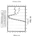
- Figure 19 shows the power efficiency and the external efficiency against drive voltage for a device similar to that of figures 15 and 16 but in which the emissive layer is mixed as (F8:F8BT [0.95:0.05]):TFB[0.5:0.5].
- Table 3 Amount of TFB in emissive layer (%) Peak power efficiency (Im/W) Voltage at peak power efficiency (V) Peak external efficiency (Cd/A) Voltage at peak external efficiency (V) 0 2.4 6.8 5.2 Approx. 8.5 25 6 3.8 8 4.5 50 6.7 3.5 7.8 3.8
- Efficiencies of greater than 20Im/W may be achieved using these 5FBBT:TFB 80:20 structures with PEDOT:PSS as the hole-transport layer. (See figure 22 ).
- the TFB promotes hole injection into the polymer matrix of the emissive layer, allowing exciplexes to form.
- the exciplexes have a relatively high probability of forming excitons on the F8BT polymer because of the higher internal field and because by doing so they can reduce energy by Forster transfer (F8BT having the narrowest optical gap in the matrix). This leads to an improvement in the external efficiency and the power efficiency.
- the efficiency of this device may be further improved by including in the emissive layer one or more other polymers whose HOMO levels are between those of the TFB and the F8 (e.g. around 5.5 eV). This should promote excitation of holes from the TFB to the emissive material, and at higher bias fields promote hole injection into the matrix of the emissive layer itself.
- PFM in the green-emissive blend substantially reduces device efficiency. This is believed to be due to its relatively shallow HOMO level, which acts as a deep hole trap, rather than as an intermediary, and thus inhibits formation of excitons on the F8BT polymer.
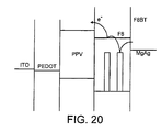
- FIGS 20 to 27 illustrate some other embodiments of the principles discussed above.
- the emissive layer is a mixture of F8BT, F8 and PPV.
- the F8BT:F8 blend is coated over the PPV and acts as an electron transport layer allowing electron transport between the cathode and the conduction band in the PPV.
- the addition of the F8BT and F8 to the PPV allows the use of a cathode that is more stable than the usual AlLi cathodes, even though it has a higher workfunction.
- the cathode is Mg, whose workfunction is 3.5 eV.
- An alternative is Al, whose workfunction is 4.2 eV.
- a further improvement could be made by including in the blend a third polymer with a LUMO level between those of F8BT (3.4 eV) and F8 (2.8 eV).
- the emissive layer is a mixture of poly(paraphenylene) ("PPP"), TFB and F8 with a CaAl cathode.
- PPP poly(paraphenylene)
- TFB poly(paraphenylene)
- F8 poly(paraphenylene)
- CaAl cathode a poly(paraphenylene)
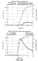
- Figure 22 illustrates the effect of the addition of TFB to a fluorene-based emitter system.
- the upper panel of figure 22 shows the luminance and luminous intensity at a range of voltages for a device in which the emissive layer is 5F8BT.
- the lower panel of figure 22 shows equivalent data for a device in which the emissive layer is 5F8BT with 20% TFB.
- Both devices have a PEDOT:PSS hole transport layer.
- the results show that the addition of TFB to the emissive layer improves peak efficiency from around 3.5lm/W to around 20lm/W. It has been found that PEDOT:PSS is superior to BFA as a hole transport layer in such devices, especially when "electronic grade" PEDOT:PSS is used.
- Figures 23 to 25 show data for devices in which the emissive component is not fluorene-based.
- Figure 23 shows a set of plots of luminance (Cd/m 2 ), current density (mA/CM 2 ), luminous efficiency (lm/W) and external efficiency (Cd/A) at a range of voltages for an 8 pixel device in which the emissive layer is the soluble PPV emitter Bis-DMOS PPV (bis dimethyl octyl silyl poly phenylene vinylene, with two side units of the formula being SiMe 2 C 8 H 17 on the phenyl ring, see figure 27 ).
- the emissive layer was spun on to hole transport layers of PEDOT:PSS.
- Figure 24 shows equivalent data for devices in which the emissive layer is Bis-DMOS PPV with 25% TFB.
- the addition of the TFB was found to improve turn-on voltage from around 3.5 to around 2.5V and to increase the efficiency to around 2.0lm/W.
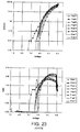
- Figure 25 shows plots of the characteristics of a series of devices in which the emissive layer is formed from another soluble PPV (PPV A of table 1) with additions of 0%, 2%, 10% or 20% TFB.
- the upper panel of figure 25 plots the current density of such devices against voltage.
- the middle panel of figure 25 plots the luminance of such devices against voltage.
- the lower panel of figure 25 shows the luminance of such devices at a constant voltage of 5.6V. The luminance and current density was found to increase with increasing TFB content.
- Figure 26 shows a set of plots of luminance (Cd/m 2 ), current density (mA/cm 2 ), luminous efficiency (lm/W) and external efficiency (Cd/A) at a range of voltages for a 4 pixel device in which the emissive layer was formed from a mixture of 70% 5F8BT and 30% of a polyethylene-based polymer with TPD-based side-chains.
- the maximum efficiency was found to be 8lm/W whereas similar devices in which the emissive layer was of 5F8BT alone were found to have maximum efficiencies of 2lm/W.
- Figure 29 shows a cyclic voltammetry oxidation sweep of the polyethylene-based polymer with TPD-based side-chains, showing that its HOMO level is in the region of 5.25eV, i.e. between that of the emissive component and that of the hole-injecting layer.
- a degree of surface phase separation will occur, with one or more of the components of the light-emissive layer increasing in concentration near a surface of the emissive layer due to the interactions of the material(s) of the emissive layer with the adjacent surfaces.
- Methods that could be used for detecting such separation include an atomic force microscope in tapping mode, and other similar techniques.
- Figure 28 shows plots of luminance at a range of voltages for a pair of devices in which the emissive layer is formed from a blend of 5F8BT:TFB (4:1) deposited over a hole transport layer of PEDOT:PSS.
- the emissive blend was deposited directly on to the PEDOT:PSS.
- line B a thin intermediate layer of TFB was deposited directly on to the PEDOT:PSS and the emissive blend was then deposited over that layer.
- Figure 28 shows that the device having the intermediate layer of TFB was found to show significantly increased luminance at fixed voltage.
- TFB concentration gradient of the TFB component in the blend as a result of greater attraction of that component to the intermediate TFB layer than of the 5F8BT. Since the TFB is capable of acting as a hole transport/capture component in the blend it may be expected to be advantageous for that component to be more concentrated towards the hole-injecting side of the emissive layer, i.e. nearer to the interface with the PEDOT:PSS. Similar results could be expected from other methods of encouraging such a concentration gradient and from the creation of an analogous concentration gradient of any electron transport/capture component towards the electron-injecting side of the emissive layer.
- table 4 shows the peak luminous efficiencies found for four device types under test: Table 4 Composition of emissive layer Intermediate layer of TFB? Peak luminous efficiency (lm/W) 5F8BT No 6 5F8BT Yes 8 5F8BT:TFB (4:1) No 9 5F8BT:TFB (4:1) Yes 12
- a multi-component layer of the types described above is preferably deposited as a single layer.
- the components that are to make up the layer are preferably combined together before or during deposition.
- Such combination suitably involves forming a material that includes the components, for example by physically mixing the components together or by forming a chemical mixture by (for instance) forming molecules that incorporate one or more of the components.
- One example of a material in which the components are combined chemically is a terpolymer of F8, F8BT and TFB, for example (5F8BT):TFB [80:20].
- a material may be formed by the following method. A 500ml r.b.
- the mixture is stirred rapidly and heated at 115 °C (oil bath temperature) for up to 18 hours.
- a further 100ml of toluene is added along with bromobenzene (1ml), the mixture is then allowed to stir at temperature (115°C oil bath temperature) for a further three hours.
- Phenyl boronic acid (1.5g) is then added and the mixture is stirred at temperature for one hour and then allowed to cool to room temperature.
- the reaction mixture is then poured slowly into 4 of methanol to precipitate the polymer.
- the polymer may then be deposited (for instance from solution) to form an emissive layer of a light-emissive device.
- one route for formation of suitable terpolmers may be to partially react monomers providing two of the components and then to add monomers providing a third component and allow the polymerisation to continue.
- the copolymers could be of any appropriate form, for example random, block or branched copolymers.
- Molecules containing both hole transporting and light emitting components may be physically combined with an electron transporting species to produce an efficient light-emitting layer.
- molecules containing both electron transporting and light emitting components may be physically combined with a hole transporting species. If one of the electrodes is especially effective then an efficient LED structure may be produced by omitting the charge transporting component corresponding to that electrode and using for the emissive layer a two component molecule, comprising a suitable opposite charge transporting component and a light emitting component.
- Two components of the emissive layer could be mixed chemically into a single molecule, and that material mixed physically with a third component provided by a second molecule.
- the devices described above can be fabricated in the conventional way, by deposition of the polymer layers from solution on to a commercially-available glass/ITO substrate, followed by evaporative deposition of the cathode.
- the fabrication of the device of figures 4 and 5 will be described in detail.
- the BFA is deposited by spin-coating from a 0.8% concentration solution with N,N- Dimethylformamide ("DMF") as the solvent.
- DMF N,N- Dimethylformamide
- the polymer layer is then dried by heating the sample to 80°C under nitrogen gas for 30 minutes.
- the emissive layer is spin-coated from a 1.6% concentration solution with mixed xylene as the solvent.
- Targets for the thicknesses of the BFA layer and the emissive layer are 10 to 80nm and 60 to 200nm respectively; typical thicknesses are 65nm and 95nm respectively.
- the cathode is deposited by evaporation to form a 20nm thick layer of Li, followed by a 200nm layer of Al.
- an inert atmosphere such as nitrogen the device is encapsulated by sealing within a glass/epoxy encapsulant.
- alternative materials for the anode include tin oxide ("TO") and flurinated TO; alternative materials for the hole transport layer include PEDOT:PSS and poly-aniline; alternative materials for the emissive layer include PPV and MEH-PPV; and alternative materials for the cathode include Li, Ba, Mg, Ca, Ce, Cs, Eu, Rb, K, Sm, Na, Sm, Sr, Tb and Yb; an alloy of two or more of such metals; a fluoride, carbide, oxide or nitride of one or more of such metals (e.g.
- the cathode could be transparent.
- the hole transport layer could be omitted, or there could be more than one hole transport layer.
- the hole transport layer could be of a mixture of materials. For instance, it could be of BFA blended with a PFM-like polymer but with solution solvency as for the BFA adjusted by the inclusion of carboxylic acid groups. Any electron transport layer could also comprise a mixture of materials, such as F8 and F8BT.
- the principles described above could be used for longer wavelength (e.g. red) emissive devices.
- red e.g.
- polymers that are highly desirable for such devices because they have deep LUMO levels, which would allow higher workfunction and more stable metals to be used for the cathode, and high PL efficiency.
- those polymers have correspondingly deep HOMO levels. The principles described above would allow those polymers to be used despite their deep HOMO levels.
- the components can suitably be mixed together before deposition.
- the components in the emissive layer are partially or fully phase-separated, so that within the emissive layer there are dispersed regions of each component (see US 5,760,791 ).
- the structure of the mixed layer should preferably provide for adequate interfaces between those components.
- each component could be dispersed evenly through the layer or it may be advantageous for one or more of the components to be concentrated near one or other of the interfaces of the light-emissive layer with the charge carrier injection layers. It may be found desirable for there to be a greater concentration of a hole-injecting material at the side of the emissive layer nearer the anode (and less at the side nearer the cathode). It may be found desirable for there to be a greater concentration of an electron-injecting material at the side of the emissive layer nearer the cathode (and less at the side nearer the anode).
- the mixed layer including the profile of the various components through the layer
- a number of techniques may be used.
- the surface interactions between one or more of the components and other layers of the device may be employed to promote some degree of phase separation in the emissive layer.
- the deposition conditions may be arranged so that the appropriate one of the hole- or electron-transport materials is preferentially attracted to or repelled from the layer on which the emissive layer is deposited.
- the hole-injecting material is preferentially attracted to that surface and/or the electron-injecting material is preferentially repelled from the surface.
- the emissive layer is deposited on an electron-injecting cathode layer.
- the material of the surface on to which the emissive layer is to be deposited may be treated or selected to give rise to such preferential effects. Where two or more of the components of the emissive layer are combined in the same molecule the way in which they are combined may be used to promote a desired state of phase separation (or segregation) or uniformity.
- the combined molecules could be synthesised as suitable random, block or branched copolymers to achieve the desired effect.
- Other factors relevant for phase separation include the solvent used (e.g. chloroform or xylene), the solvent vapour pressure, the molecular weight, component surface energies (relative to each other and/or to the free surface on to which the emissive layer is deposited), poly dispersity, component volume fractions, structural features etc.
Landscapes
- Chemical & Material Sciences (AREA)
- Physics & Mathematics (AREA)
- Optics & Photonics (AREA)
- Engineering & Computer Science (AREA)
- Materials Engineering (AREA)
- Organic Chemistry (AREA)
- Electroluminescent Light Sources (AREA)
Applications Claiming Priority (2)
| Application Number | Priority Date | Filing Date | Title |
|---|---|---|---|
| GBGB9805476.0A GB9805476D0 (en) | 1998-03-13 | 1998-03-13 | Electroluminescent devices |
| EP99907774A EP1062703B1 (en) | 1998-03-13 | 1999-03-12 | Electroluminescent devices |
Related Parent Applications (2)
| Application Number | Title | Priority Date | Filing Date |
|---|---|---|---|
| EP99907774.6 Division | 1999-03-12 | ||
| EP99907774A Division EP1062703B1 (en) | 1998-03-13 | 1999-03-12 | Electroluminescent devices |
Publications (3)
| Publication Number | Publication Date |
|---|---|
| EP1993155A2 EP1993155A2 (en) | 2008-11-19 |
| EP1993155A3 EP1993155A3 (en) | 2012-05-02 |
| EP1993155B1 true EP1993155B1 (en) | 2016-05-11 |
Family
ID=10828566
Family Applications (5)
| Application Number | Title | Priority Date | Filing Date |
|---|---|---|---|
| EP10184247.4A Withdrawn EP2267819A3 (en) | 1998-03-13 | 1999-03-12 | Electroluminescent devices |
| EP08162422.3A Expired - Lifetime EP1993155B1 (en) | 1998-03-13 | 1999-03-12 | Electroluminescent devices |
| EP99907774A Expired - Lifetime EP1062703B1 (en) | 1998-03-13 | 1999-03-12 | Electroluminescent devices |
| EP10167983.5A Expired - Lifetime EP2228847B1 (en) | 1998-03-13 | 1999-03-12 | Electroluminescent devices |
| EP06075642A Withdrawn EP1672719A3 (en) | 1998-03-13 | 1999-03-12 | Electroluminescent devices |
Family Applications Before (1)
| Application Number | Title | Priority Date | Filing Date |
|---|---|---|---|
| EP10184247.4A Withdrawn EP2267819A3 (en) | 1998-03-13 | 1999-03-12 | Electroluminescent devices |
Family Applications After (3)
| Application Number | Title | Priority Date | Filing Date |
|---|---|---|---|
| EP99907774A Expired - Lifetime EP1062703B1 (en) | 1998-03-13 | 1999-03-12 | Electroluminescent devices |
| EP10167983.5A Expired - Lifetime EP2228847B1 (en) | 1998-03-13 | 1999-03-12 | Electroluminescent devices |
| EP06075642A Withdrawn EP1672719A3 (en) | 1998-03-13 | 1999-03-12 | Electroluminescent devices |
Country Status (10)
| Country | Link |
|---|---|
| US (6) | US6897473B1 (enExample) |
| EP (5) | EP2267819A3 (enExample) |
| JP (5) | JP2002507825A (enExample) |
| KR (6) | KR100977302B1 (enExample) |
| CN (5) | CN100589259C (enExample) |
| AU (1) | AU2740299A (enExample) |
| DE (1) | DE69939815D1 (enExample) |
| GB (1) | GB9805476D0 (enExample) |
| TW (1) | TW525409B (enExample) |
| WO (1) | WO1999048160A1 (enExample) |
Families Citing this family (237)
| Publication number | Priority date | Publication date | Assignee | Title |
|---|---|---|---|---|
| US6309763B1 (en) * | 1997-05-21 | 2001-10-30 | The Dow Chemical Company | Fluorene-containing polymers and electroluminescent devices therefrom |
| GB9805476D0 (en) | 1998-03-13 | 1998-05-13 | Cambridge Display Tech Ltd | Electroluminescent devices |
| KR100697861B1 (ko) * | 1998-03-13 | 2007-03-22 | 캠브리지 디스플레이 테크놀로지 리미티드 | 전장 발광 디바이스들 |
| DE19846768A1 (de) * | 1998-10-10 | 2000-04-20 | Aventis Res & Tech Gmbh & Co | Konjugierte Polymere enthaltend 2,7-Fluorenyleinheiten mit verbesserten Eigenschaften |
| EP1155096B1 (en) * | 1999-02-04 | 2005-03-09 | Dow Global Technologies Inc. | Fluorene copolymers and devices made therefrom |
| EP2267816A1 (en) * | 1999-03-12 | 2010-12-29 | Sumitomo Chemical Company, Limited | Polymers, their preparation and uses |
| KR20010090848A (ko) * | 1999-10-05 | 2001-10-19 | 모리시타 요이찌 | 발광소자와 그 제조방법, 및 그것을 이용한 표시장치,조명장치 |
| JP5069393B2 (ja) * | 2000-09-26 | 2012-11-07 | ケンブリッジ ディスプレイ テクノロジー リミテッド | ポリマーおよびその使用方法 |
| ATE333481T1 (de) | 2000-09-26 | 2006-08-15 | Cambridge Display Tech Ltd | Tordierte polymere, verwendung und verfahren zur herstellung statistischer polymere |
| ATE358170T1 (de) | 2000-10-03 | 2007-04-15 | Cambridge Display Tech Ltd | Lichtemittierende polymermischungen und daraus hergestellte lichtemittierende anordnungen |
| US6803720B2 (en) * | 2000-12-15 | 2004-10-12 | Universal Display Corporation | Highly stable and efficient OLEDs with a phosphorescent-doped mixed layer architecture |
| EP1366046B1 (en) | 2001-01-24 | 2006-10-18 | Cambridge Display Technology Limited | Monomer for use in preparation of a polymer to be used in optical devices |
| GB0109108D0 (en) | 2001-04-11 | 2001-05-30 | Cambridge Display Tech Ltd | Polymer, its preparation and uses |
| GB0109295D0 (en) * | 2001-04-12 | 2001-05-30 | Univ Cambridge Tech | Optoelectronic devices and a method for producing the same |
| US7632908B2 (en) | 2001-05-11 | 2009-12-15 | Cambridge Display Technology Limited | Substituted fluorene polymers, their preparation and use in optical devices |
| EP1388180A2 (en) | 2001-05-18 | 2004-02-11 | Cambridge University Technical Services Limited | Electroluminescent device |
| US7351788B2 (en) * | 2001-06-22 | 2008-04-01 | Cambridge Display Technology Limited | Polymer containing substituted triphenylamine units |
| EP1921688B1 (en) | 2001-07-10 | 2011-03-30 | Dow Global Technologies Inc. | Electroactive polymers and devices made therefrom |
| GB2379317A (en) | 2001-08-30 | 2003-03-05 | Cambridge Display Tech Ltd | Optoelectronic display operating by photoluminescence quenching |
| GB0125620D0 (en) | 2001-10-25 | 2001-12-19 | Cambridge Display Tech Ltd | Monomers and low band gap polymers formed therefrom |
| GB2381643A (en) | 2001-10-31 | 2003-05-07 | Cambridge Display Tech Ltd | Display drivers |
| GB2381644A (en) | 2001-10-31 | 2003-05-07 | Cambridge Display Tech Ltd | Display drivers |
| GB2386462A (en) | 2002-03-14 | 2003-09-17 | Cambridge Display Tech Ltd | Display driver circuits |
| SG128438A1 (en) | 2002-03-15 | 2007-01-30 | Sumitomo Chemical Co | Polymer compound and polymer light emitting deviceusing the same |
| GB0209502D0 (en) | 2002-04-25 | 2002-06-05 | Cambridge Display Tech Ltd | Display driver circuits |
| GB2388236A (en) | 2002-05-01 | 2003-11-05 | Cambridge Display Tech Ltd | Display and driver circuits |
| US7696303B2 (en) | 2002-05-10 | 2010-04-13 | Cambridge Display Technology Limited | Polymers their preparation and uses |
| DE10224021B4 (de) * | 2002-05-24 | 2006-06-01 | Novaled Gmbh | Phosphoreszentes lichtemittierendes Bauelement mit organischen Schichten |
| GB2389952A (en) | 2002-06-18 | 2003-12-24 | Cambridge Display Tech Ltd | Driver circuits for electroluminescent displays with reduced power consumption |
| GB2389951A (en) | 2002-06-18 | 2003-12-24 | Cambridge Display Tech Ltd | Display driver circuits for active matrix OLED displays |
| SG119187A1 (en) | 2002-06-28 | 2006-02-28 | Semiconductor Energy Lab | Light emitting device and manufacturing method therefor |
| US7265378B2 (en) | 2002-07-10 | 2007-09-04 | E. I. Du Pont De Nemours And Company | Electronic devices made with electron transport and/or anti-quenching layers |
| JP5073151B2 (ja) * | 2002-07-22 | 2012-11-14 | 住友化学株式会社 | 共重合体およびそれを用いた高分子発光素子 |
| US7531377B2 (en) | 2002-09-03 | 2009-05-12 | Cambridge Display Technology Limited | Optical device |
| KR101002822B1 (ko) | 2002-10-30 | 2010-12-21 | 스미또모 가가꾸 가부시키가이샤 | 고분자 화합물 및 이를 이용한 고분자 발광 소자 |
| GB0225869D0 (en) | 2002-11-06 | 2002-12-11 | Cambridge Display Tech Ltd | Polymer |
| GB0226010D0 (en) | 2002-11-08 | 2002-12-18 | Cambridge Display Tech Ltd | Polymers for use in organic electroluminescent devices |
| JP4152173B2 (ja) * | 2002-11-18 | 2008-09-17 | 出光興産株式会社 | 有機エレクトロルミネッセンス素子 |
| GB0227778D0 (en) | 2002-11-28 | 2003-01-08 | Cambridge Display Tech Ltd | Droplet-deposition related methods and apparatus |
| US6916902B2 (en) * | 2002-12-19 | 2005-07-12 | Dow Global Technologies Inc. | Tricyclic arylamine containing polymers and electronic devices therefrom |
| CN100479628C (zh) * | 2002-12-27 | 2009-04-15 | 富士胶片株式会社 | 有机电致发光设备 |
| GB0300105D0 (en) * | 2003-01-03 | 2003-02-05 | Cambridge Display Tech Ltd | Ablation methods & apparatus |
| GB0306409D0 (en) | 2003-03-20 | 2003-04-23 | Cambridge Display Tech Ltd | Electroluminescent device |
| GB0306414D0 (en) * | 2003-03-20 | 2003-04-23 | Cambridge Display Tech Ltd | Polymers,their preparations and uses |
| JP2007504342A (ja) | 2003-05-30 | 2007-03-01 | メルク パテント ゲーエムベーハー | ポリマー |
| EP1491568A1 (en) | 2003-06-23 | 2004-12-29 | Covion Organic Semiconductors GmbH | Semiconductive Polymers |
| US20050019607A1 (en) * | 2003-06-30 | 2005-01-27 | Franky So | OLED device with mixed emissive layer |
| GB0321781D0 (en) | 2003-09-17 | 2003-10-15 | Toppan Printing Company Ltd | Electroluminescent device |
| US20050069727A1 (en) * | 2003-09-30 | 2005-03-31 | Rahul Gupta | Oled emissive polymer layer |
| WO2005049695A1 (en) | 2003-10-28 | 2005-06-02 | Ciba Specialty Chemicals Holding Inc. | Novel diketopyrrolopyrrole polymers |
| EP1682600B1 (en) | 2003-11-10 | 2013-01-23 | Cambridge Display Technology Limited | Dibenzosilol polymers, their preparation and uses |
| GB0326853D0 (en) * | 2003-11-19 | 2003-12-24 | Cambridge Display Tech Ltd | Optical device |
| JP5230942B2 (ja) * | 2003-12-13 | 2013-07-10 | メルク パテント ゲーエムベーハー | オリゴマーおよびポリマー |
| GB0329364D0 (en) * | 2003-12-19 | 2004-01-21 | Cambridge Display Tech Ltd | Optical device |
| GB0401613D0 (en) | 2004-01-26 | 2004-02-25 | Cambridge Display Tech Ltd | Organic light emitting diode |
| GB2410600A (en) | 2004-01-30 | 2005-08-03 | Cambridge Display Tech Ltd | Organic light emitting diode display device |
| JP5092199B2 (ja) * | 2004-02-02 | 2012-12-05 | 住友化学株式会社 | 有機エレクトロルミネッセンス素子 |
| TWI270318B (en) * | 2004-03-30 | 2007-01-01 | Osram Opto Semiconductors Gmbh | Device structure to improve OLED reliability |
| US7737632B2 (en) * | 2004-04-27 | 2010-06-15 | Fujifilm Corporation | Organic EL element with lamination structure and its manufacturing method |
| US9136504B2 (en) | 2004-08-04 | 2015-09-15 | Cambridge Display Technology Limited | Organic electroluminescent device |
| US7540978B2 (en) | 2004-08-05 | 2009-06-02 | Novaled Ag | Use of an organic matrix material for producing an organic semiconductor material, organic semiconductor material and electronic component |
| EP1627891A1 (en) | 2004-08-11 | 2006-02-22 | Covion Organic Semiconductors GmbH | Polymers for use in organic electroluminescent devices |
| KR101027896B1 (ko) | 2004-08-13 | 2011-04-07 | 테크니셰 유니베르시테트 드레스덴 | 발광 컴포넌트를 위한 층 어셈블리 |
| JP4238194B2 (ja) * | 2004-09-17 | 2009-03-11 | セイコーエプソン株式会社 | 有機エレクトロルミネッセンス装置、有機エレクトロルミネッセンス装置の製造方法、電子機器 |
| JP4916102B2 (ja) * | 2004-09-24 | 2012-04-11 | シャープ株式会社 | 有機el素子 |
| GB0421712D0 (en) * | 2004-09-30 | 2004-11-03 | Cambridge Display Tech Ltd | Multi-line addressing methods and apparatus |
| GB0421711D0 (en) * | 2004-09-30 | 2004-11-03 | Cambridge Display Tech Ltd | Multi-line addressing methods and apparatus |
| GB0421710D0 (en) * | 2004-09-30 | 2004-11-03 | Cambridge Display Tech Ltd | Multi-line addressing methods and apparatus |
| GB0428191D0 (en) | 2004-12-23 | 2005-01-26 | Cambridge Display Tech Ltd | Digital signal processing methods and apparatus |
| BRPI0516867A (pt) * | 2004-09-30 | 2008-09-23 | Cambridge Display Tech Ltd | métodos e aparelhos de endereçamento de linha múltipla |
| DE602004006275T2 (de) | 2004-10-07 | 2007-12-20 | Novaled Ag | Verfahren zur Dotierung von einem Halbleitermaterial mit Cäsium |
| DE112005002495B4 (de) | 2004-10-11 | 2016-11-17 | Cambridge Display Technology Ltd. | Polares halbleitendes Lochtransportmaterial |
| JP4653469B2 (ja) | 2004-12-01 | 2011-03-16 | 出光興産株式会社 | 有機電界発光素子 |
| GB0427965D0 (en) | 2004-12-22 | 2005-01-26 | Cambridge Display Technology O | Process for the synthesis of arylfluorenes and analogues thereof |
| US9179518B2 (en) | 2004-12-24 | 2015-11-03 | Cambridge Display Technology Limited | Light emissive device |
| GB0428444D0 (en) | 2004-12-29 | 2005-02-02 | Cambridge Display Tech Ltd | Conductive polymer compositions in opto-electrical devices |
| GB0428445D0 (en) | 2004-12-29 | 2005-02-02 | Cambridge Display Tech Ltd | Blue-shifted triarylamine polymer |
| GB2436996B8 (en) | 2004-12-29 | 2013-12-11 | Cambridge Display Tech Ltd | Rigid amines |
| KR101074786B1 (ko) * | 2004-12-31 | 2011-10-19 | 삼성모바일디스플레이주식회사 | 트리페닐아민 유도체 구조를 함유한 폴리이미드를 포함한 전자차단층을 채용한 유기 전계 발광 소자 |
| JP4450207B2 (ja) * | 2005-01-14 | 2010-04-14 | セイコーエプソン株式会社 | 発光素子の製造方法 |
| EP1705727B1 (de) * | 2005-03-15 | 2007-12-26 | Novaled AG | Lichtemittierendes Bauelement |
| US7683536B2 (en) | 2005-03-31 | 2010-03-23 | The Trustees Of Princeton University | OLEDs utilizing direct injection to the triplet state |
| EP1818996A1 (de) | 2005-04-13 | 2007-08-15 | Novaled AG | Anordnung für eine organische Leuchtdiode vom pin-Typ und Verfahren zum Herstellen |
| GB0507684D0 (en) | 2005-04-15 | 2005-05-25 | Cambridge Display Tech Ltd | Pulsed driven displays |
| GB0510382D0 (en) | 2005-05-20 | 2005-06-29 | Cambridge Display Tech Ltd | Ink jet printing compositions in opto-electrical devices |
| EP1727221B1 (de) * | 2005-05-27 | 2010-04-14 | Novaled AG | Transparente organische Leuchtdiode |
| EP1729346A1 (de) * | 2005-06-01 | 2006-12-06 | Novaled AG | Lichtemittierendes Bauteil mit einer Elektrodenanordnung |
| JP5119611B2 (ja) * | 2005-06-01 | 2013-01-16 | 住友化学株式会社 | 高分子組成物および高分子発光素子 |
| EP1739765A1 (de) * | 2005-07-01 | 2007-01-03 | Novaled AG | Organische Leuchtdiode und Anordnung mit mehreren organischen Leuchtdioden |
| GB0514476D0 (en) * | 2005-07-14 | 2005-08-17 | Cambridge Display Tech Ltd | Conductive polymer compositions in opto-electrical devices |
| TW200718726A (en) | 2005-08-12 | 2007-05-16 | Sumitomo Chemical Co | Polymer and polymer light-emitting element using the same |
| GB0517195D0 (en) | 2005-08-23 | 2005-09-28 | Cambridge Display Tech Ltd | Molecular electronic device structures and fabrication methods |
| DE112006002220B4 (de) | 2005-08-23 | 2018-05-24 | Cambridge Display Technology Ltd. | Organische elektronische Vorrichtungsstrukturen und Herstellungsverfahren |
| KR101193179B1 (ko) * | 2005-08-26 | 2012-10-19 | 삼성디스플레이 주식회사 | 오가노실록산 화합물 및 이를 구비한 유기 발광 소자 |
| GB2430069A (en) | 2005-09-12 | 2007-03-14 | Cambridge Display Tech Ltd | Active matrix display drive control systems |
| GB0518968D0 (en) | 2005-09-16 | 2005-10-26 | Cdt Oxford Ltd | Organic light-emitting device |
| US7982212B2 (en) | 2005-10-07 | 2011-07-19 | Sumitomo Chemical Company, Limited | Copolymer and polymer light emitting device using the same |
| GB2431276B (en) | 2005-10-14 | 2008-11-12 | Cambridge Display Tech Ltd | Display monitoring systems |
| KR20080066084A (ko) | 2005-11-11 | 2008-07-15 | 스미또모 가가꾸 가부시키가이샤 | 공액 고분자 화합물 및 이를 이용한 고분자 발광 소자 |
| KR101193180B1 (ko) * | 2005-11-14 | 2012-10-19 | 삼성디스플레이 주식회사 | 전도성 고분자 조성물 및 이로부터 얻은 막을 구비한 전자소자 |
| KR20080068134A (ko) | 2005-11-18 | 2008-07-22 | 스미또모 가가꾸 가부시키가이샤 | 고분자 화합물 및 이를 이용한 고분자 발광 소자 |
| KR101243917B1 (ko) * | 2005-12-19 | 2013-03-14 | 삼성디스플레이 주식회사 | 전도성 고분자 조성물 및 이로부터 얻은 막을 구비한 전자소자 |
| EP1806795B1 (de) * | 2005-12-21 | 2008-07-09 | Novaled AG | Organisches Bauelement |
| GB0526185D0 (en) | 2005-12-22 | 2006-02-01 | Cambridge Display Tech Ltd | Electronic device |
| GB2433638B (en) | 2005-12-22 | 2011-06-29 | Cambridge Display Tech Ltd | Passive matrix display drivers |
| GB2433509A (en) | 2005-12-22 | 2007-06-27 | Cambridge Display Tech Ltd | Arylamine polymer |
| GB0526393D0 (en) | 2005-12-23 | 2006-02-08 | Cdt Oxford Ltd | Light emissive device |
| EP1804308B1 (en) * | 2005-12-23 | 2012-04-04 | Novaled AG | An organic light emitting device with a plurality of organic electroluminescent units stacked upon each other |
| DE602006001930D1 (de) * | 2005-12-23 | 2008-09-04 | Novaled Ag | tur von organischen Schichten |
| GB2448098B (en) | 2005-12-28 | 2011-07-06 | Sumitomo Chemical Co | Block copolymer |
| EP1808909A1 (de) | 2006-01-11 | 2007-07-18 | Novaled AG | Elekrolumineszente Lichtemissionseinrichtung |
| US7968904B2 (en) * | 2006-02-06 | 2011-06-28 | Fujifilm Corporation | Organic electroluminescence device |
| JP2007220772A (ja) * | 2006-02-15 | 2007-08-30 | Idemitsu Kosan Co Ltd | 有機エレクトロルミネッセンス用高分子化合物及びその製造方法 |
| GB2437113B (en) | 2006-04-12 | 2008-11-26 | Cambridge Display Tech Ltd | Light-emissive display and method of manufacturing the same |
| KR20070101984A (ko) * | 2006-04-13 | 2007-10-18 | 삼성에스디아이 주식회사 | 전하분리층을 구비한 유기 전기발광 소자 |
| EP1848049B1 (de) * | 2006-04-19 | 2009-12-09 | Novaled AG | Lichtemittierendes Bauelement |
| GB2440934B (en) | 2006-04-28 | 2009-12-16 | Cdt Oxford Ltd | Opto-electrical polymers and devices |
| US20070275265A1 (en) * | 2006-05-25 | 2007-11-29 | Au Optronics Corporation | Organic light emitting layer with a reduced phosphorescent dopant concentration and applications of same |
| GB2439358B (en) | 2006-06-19 | 2010-12-15 | Cambridge Display Tech Ltd | Organic electroluminescent optocouplers |
| JP5461181B2 (ja) * | 2006-07-25 | 2014-04-02 | メルク パテント ゲーエムベーハー | ポリマーブレンドとその有機発光素子での使用 |
| CA2657126A1 (en) | 2006-07-28 | 2008-01-31 | Ciba Holding Inc. | Novel polymers |
| WO2008015422A2 (en) | 2006-08-01 | 2008-02-07 | Cambridge Display Technology Limited | Methods of manufacturing opto-electrical devices |
| TW200818981A (en) | 2006-08-30 | 2008-04-16 | Sumitomo Chemical Co | Organic electroluminescence device |
| GB2441355B (en) | 2006-08-31 | 2009-05-20 | Cambridge Display Tech Ltd | Organic electronic device |
| GB0617167D0 (en) | 2006-08-31 | 2006-10-11 | Cdt Oxford Ltd | Compounds for use in opto-electrical devices |
| GB2441354B (en) | 2006-08-31 | 2009-07-29 | Cambridge Display Tech Ltd | Display drive systems |
| US20100038658A1 (en) * | 2006-09-11 | 2010-02-18 | Vanderbilt University | Polymer light-emitting diode and fabrication of same by resonant infrared laser vapor deposition |
| US8927115B2 (en) | 2006-09-14 | 2015-01-06 | Sumitomo Chemical Company, Limited | Organic electroluminescent device |
| JP2008098619A (ja) * | 2006-09-14 | 2008-04-24 | Sumitomo Chemical Co Ltd | 有機エレクトロルミネッセンス素子 |
| GB0618698D0 (en) | 2006-09-22 | 2006-11-01 | Cambridge Display Tech Ltd | Molecular electronic device fabrication methods and structures |
| CN101517034A (zh) * | 2006-09-26 | 2009-08-26 | 住友化学株式会社 | 高分子吸附膜及其制造方法 |
| GB0620045D0 (en) | 2006-10-10 | 2006-11-22 | Cdt Oxford Ltd | Otpo-electrical devices and methods of making the same |
| DE102006059509B4 (de) * | 2006-12-14 | 2012-05-03 | Novaled Ag | Organisches Leuchtbauelement |
| GB2448175B (en) | 2007-04-04 | 2009-07-22 | Cambridge Display Tech Ltd | Thin film transistor |
| DE102007019260B4 (de) * | 2007-04-17 | 2020-01-16 | Novaled Gmbh | Nichtflüchtiges organisches Speicherelement |
| JP5374908B2 (ja) | 2007-04-27 | 2013-12-25 | 住友化学株式会社 | ピレン系高分子化合物及びそれを用いてなる発光素子 |
| JP5248910B2 (ja) | 2007-05-30 | 2013-07-31 | 住友化学株式会社 | 有機エレクトロルミネッセンス素子および該素子を用いた表示装置 |
| JP2009021104A (ja) | 2007-07-12 | 2009-01-29 | Sumitomo Chemical Co Ltd | 有機発光素子の製造方法 |
| GB2453374A (en) | 2007-10-05 | 2009-04-08 | Cambridge Display Tech Ltd | Matching multiple current sources/sinks |
| GB2453375A (en) | 2007-10-05 | 2009-04-08 | Cambridge Display Tech Ltd | Driving a display using an effective analogue drive signal generated from a modulated digital signal |
| GB0721567D0 (en) | 2007-11-02 | 2007-12-12 | Cambridge Display Tech Ltd | Pixel driver circuits |
| GB2454867B (en) | 2007-11-09 | 2010-02-03 | Cambridge Display Tech Ltd | Electroluminescent devices comprising bus bar |
| GB2454890B (en) | 2007-11-21 | 2010-08-25 | Limited Cambridge Display Technology | Light-emitting device and materials therefor |
| JP5217931B2 (ja) | 2007-11-29 | 2013-06-19 | 住友化学株式会社 | 有機エレクトロルミネッセンス素子及びその製造方法 |
| DE102008046857B4 (de) | 2007-12-17 | 2025-03-27 | Pictiva Displays International Limited | OLED für Betrieb mit Wechselspannung und Herstellungsverfahren |
| GB2455747B (en) | 2007-12-19 | 2011-02-09 | Cambridge Display Tech Ltd | Electronic devices and methods of making the same using solution processing techniques |
| CN101911833A (zh) | 2007-12-28 | 2010-12-08 | 住友化学株式会社 | 高分子发光元件、制造方法以及高分子发光显示装置 |
| GB2456788B (en) | 2008-01-23 | 2011-03-09 | Cambridge Display Tech Ltd | White light emitting material |
| GB0803950D0 (en) | 2008-03-03 | 2008-04-09 | Cambridge Display Technology O | Solvent for printing composition |
| KR101626994B1 (ko) | 2008-03-07 | 2016-06-03 | 스미또모 가가꾸 가부시끼가이샤 | 적층 구조체 |
| GB2458454B (en) | 2008-03-14 | 2011-03-16 | Cambridge Display Tech Ltd | Electronic devices and methods of making the same using solution processing techniques |
| GB2460018B (en) | 2008-05-07 | 2013-01-30 | Cambridge Display Tech Ltd | Active matrix displays |
| GB2459895B (en) | 2008-05-09 | 2011-04-27 | Cambridge Display Technology Limited | Organic light emissive device |
| GB2462410B (en) | 2008-07-21 | 2011-04-27 | Cambridge Display Tech Ltd | Compositions and methods for manufacturing light-emissive devices |
| GB2462122B (en) | 2008-07-25 | 2013-04-03 | Cambridge Display Tech Ltd | Electroluminescent materials |
| US9318706B2 (en) | 2008-07-30 | 2016-04-19 | Sumitomo Chemical Company, Limited | Laminated structure, method for producing same, and electronic element comprising same |
| GB0814161D0 (en) | 2008-08-01 | 2008-09-10 | Cambridge Display Tech Ltd | Blue-light emitting material |
| GB2462314B (en) | 2008-08-01 | 2011-03-16 | Cambridge Display Tech Ltd | Organic light-emiting materials and devices |
| GB2462296A (en) | 2008-08-01 | 2010-02-03 | Cambridge Display Tech Ltd | Pixel driver circuits |
| DE102008036063B4 (de) * | 2008-08-04 | 2017-08-31 | Novaled Gmbh | Organischer Feldeffekt-Transistor |
| DE102008036062B4 (de) | 2008-08-04 | 2015-11-12 | Novaled Ag | Organischer Feldeffekt-Transistor |
| GB2462646B (en) | 2008-08-15 | 2011-05-11 | Cambridge Display Tech Ltd | Active matrix displays |
| GB0814971D0 (en) | 2008-08-15 | 2008-09-24 | Cambridge Display Tech Ltd | Opto-electrical devices and methods of manufacturing the same |
| GB2462844B (en) | 2008-08-21 | 2011-04-20 | Cambridge Display Tech Ltd | Organic electroluminescent device |
| GB2462688B (en) | 2008-08-22 | 2012-03-07 | Cambridge Display Tech Ltd | Opto-electrical devices and methods of manufacturing the same |
| GB2463040B (en) | 2008-08-28 | 2012-10-31 | Cambridge Display Tech Ltd | Light-emitting material |
| GB2463077B (en) | 2008-09-02 | 2012-11-07 | Sumitomo Chemical Co | Electroluminescent material and device |
| GB2463493B (en) | 2008-09-15 | 2012-11-14 | Cambridge Display Tech Ltd | An improved method for ink jet printing organic electronic devices |
| WO2010036805A2 (en) * | 2008-09-24 | 2010-04-01 | Massachusetts Institute Of Technology | Photon processing with nanopatterned materials |
| GB2464111B (en) | 2008-10-02 | 2011-06-15 | Cambridge Display Tech Ltd | Organic electroluminescent device |
| JP5515542B2 (ja) | 2008-10-06 | 2014-06-11 | 住友化学株式会社 | 含窒素複素環構造を含む高分子化合物 |
| GB2466843A (en) | 2009-01-12 | 2010-07-14 | Cambridge Display Tech Ltd | Interlayer formulation for flat films |
| GB2466842B (en) | 2009-01-12 | 2011-10-26 | Cambridge Display Tech Ltd | Interlayer formulation for flat films |
| JP5691177B2 (ja) | 2009-01-29 | 2015-04-01 | 住友化学株式会社 | 高分子化合物及びそれを用いる発光素子 |
| GB2469497B (en) | 2009-04-16 | 2012-04-11 | Cambridge Display Tech Ltd | Polymers comprising fluorene derivative repeat units and their preparation |
| GB2469498B (en) | 2009-04-16 | 2012-03-07 | Cambridge Display Tech Ltd | Polymer and polymerisation method |
| GB2469500B (en) | 2009-04-16 | 2012-06-06 | Cambridge Display Tech Ltd | Method of forming a polymer |
| GB0906554D0 (en) | 2009-04-16 | 2009-05-20 | Cambridge Display Tech Ltd | Organic electroluminescent device |
| DE102009030848A1 (de) * | 2009-06-26 | 2011-02-03 | Merck Patent Gmbh | Polymere enthaltend Struktureinheiten, die Alkylalkoxygruppen aufweisen, Blends enthaltend diese Polymere sowie optoelektronische Vorrichtungen enthaltend diese Polymere und Blends |
| GB0912041D0 (en) * | 2009-07-10 | 2009-08-19 | Cambridge Entpr Ltd | Optoelectronic devices |
| WO2011013488A1 (ja) | 2009-07-31 | 2011-02-03 | 住友化学株式会社 | 高分子発光素子 |
| GB2473240A (en) | 2009-09-04 | 2011-03-09 | Cambridge Display Tech Ltd | A touch screen device using correlated emitter-detector pairs |
| GB2473239B (en) | 2009-09-04 | 2014-07-09 | Cambridge Display Tech Ltd | Touch screen display device |
| KR101704090B1 (ko) | 2009-09-30 | 2017-02-07 | 스미또모 가가꾸 가부시키가이샤 | 적층 구조체, 중합체, 전계 발광 소자 및 광전 변환 소자 |
| TWI538561B (zh) * | 2009-10-22 | 2016-06-11 | 住友化學股份有限公司 | 有機電激發光元件 |
| GB2475247B (en) | 2009-11-10 | 2012-06-13 | Cambridge Display Tech Ltd | Organic optoelectronic device and method |
| GB2475246B (en) | 2009-11-10 | 2012-02-29 | Cambridge Display Tech Ltd | Organic opto-electronic device and method |
| JP2011146307A (ja) | 2010-01-15 | 2011-07-28 | Sumitomo Chemical Co Ltd | 高分子発光素子 |
| KR101769173B1 (ko) | 2010-01-28 | 2017-08-17 | 스미또모 가가꾸 가부시키가이샤 | 고분자 화합물 및 그것을 이용하여 이루어지는 발광 소자 |
| GB2479120A (en) | 2010-03-26 | 2011-10-05 | Cambridge Display Tech Ltd | Organic electrolumunescent device having conductive layer connecting metal over well defining layer and cathode |
| GB2487342B (en) * | 2010-05-14 | 2013-06-19 | Cambridge Display Tech Ltd | Host polymer comprising conjugated repeat units and non-conjugated repeat units for light-emitting compositions, and organic light-emitting devices |
| GB2499969A (en) | 2010-06-25 | 2013-09-11 | Cambridge Display Tech Ltd | Composition comprising an organic semiconducting material and a triplet-accepting material |
| CN102959758B (zh) | 2010-06-25 | 2016-03-23 | 剑桥显示技术有限公司 | 有机发光材料、器件和方法 |
| GB2482110B (en) | 2010-07-05 | 2014-08-27 | Cambridge Display Tech Ltd | Lighting elements |
| US9184388B2 (en) | 2010-07-29 | 2015-11-10 | Sumitomo Chemical Company, Limited | Layered structure, electronic device using same, aromatic compound, and method for manufacturing said compound |
| US20120049168A1 (en) | 2010-08-31 | 2012-03-01 | Universal Display Corporation | Cross-Linked Charge Transport Layer Containing an Additive Compound |
| GB2483269A (en) | 2010-09-02 | 2012-03-07 | Cambridge Display Tech Ltd | Organic Electroluminescent Device containing Fluorinated Compounds |
| GB2485001A (en) | 2010-10-19 | 2012-05-02 | Cambridge Display Tech Ltd | OLEDs |
| US9187600B2 (en) * | 2010-11-01 | 2015-11-17 | Basf Se | Polyimides as dielectric |
| JP5753854B2 (ja) * | 2010-11-02 | 2015-07-22 | 株式会社日立製作所 | 有機発光素子、有機発光素子形成用塗液、有機発光素子形成用材料及び当該有機発光素子を用いた光源装置並びに当該有機発光素子の製造方法 |
| GB2486202A (en) | 2010-12-06 | 2012-06-13 | Cambridge Display Tech Ltd | Adhesion layer for solution-processed transition metal oxides on inert metal contacts of organic thin film transistors. |
| GB2486203A (en) | 2010-12-06 | 2012-06-13 | Cambridge Display Tech Ltd | Transition metal oxide doped interface by deposition and drying of precursor |
| GB2487207B (en) | 2011-01-12 | 2013-07-31 | Cambridge Display Tech Ltd | Electroluminescence |
| US9783734B2 (en) | 2011-02-28 | 2017-10-10 | Kyulux, Inc. | Delayed fluorescence material and organic electroluminescence device |
| TW201245359A (en) | 2011-03-17 | 2012-11-16 | Sumitomo Chemical Co | Metal complex composition and its mixture |
| GB201105364D0 (en) | 2011-03-30 | 2011-05-11 | Cambridge Display Tech Ltd | Surface planarisation |
| GB201105582D0 (en) | 2011-04-01 | 2011-05-18 | Cambridge Display Tech Ltd | Organic light-emitting device and method |
| GB201110564D0 (en) | 2011-06-22 | 2011-08-03 | Cambridge Display Tech Ltd | Polymer and optoelectronic device |
| GB201110770D0 (en) | 2011-06-24 | 2011-08-10 | Cambridge Display Tech Ltd | Process for controlling the acceptor strength of solution-processed transition metal oxides for OLED applications |
| US9493613B2 (en) | 2011-07-04 | 2016-11-15 | Cambridge Display Technology, Ltd. | Organic light emitting composition, device and method |
| GB201111742D0 (en) | 2011-07-08 | 2011-08-24 | Cambridge Display Tech Ltd | Solution |
| GB201113563D0 (en) | 2011-08-05 | 2011-09-21 | Cambridge Display Tech Ltd | Light emitting polymers and devices |
| GB2495107A (en) | 2011-09-28 | 2013-04-03 | Cambridge Display Tech Ltd | Organic light emitting diode display device with further small-area sacrificial diodes |
| GB201210131D0 (en) | 2011-11-02 | 2012-07-25 | Cambridge Display Tech Ltd | Light emitting composition and device |
| GB201118997D0 (en) | 2011-11-03 | 2011-12-14 | Cambridge Display Tech Ltd | Electronic device and method |
| GB201200619D0 (en) | 2012-01-16 | 2012-02-29 | Cambridge Display Tech Ltd | Polymer |
| CN104093689A (zh) | 2012-01-31 | 2014-10-08 | 剑桥显示技术有限公司 | 聚合物 |
| GB201204670D0 (en) | 2012-03-16 | 2012-05-02 | Cambridge Display Tech Ltd | Optoelectronic device |
| JPWO2013190847A1 (ja) * | 2012-06-20 | 2016-02-08 | 株式会社Joled | 有機発光素子およびその製造方法 |
| GB2505893A (en) | 2012-09-13 | 2014-03-19 | Cambridge Display Tech Ltd | Compounds for use in organic optoelectronic devices |
| GB2515503A (en) | 2013-06-25 | 2014-12-31 | Cambridge Display Tech Ltd | Organic light emitting diode fabrication |
| JP2016525781A (ja) * | 2013-07-29 | 2016-08-25 | メルク、パテント、ゲゼルシャフト、ミット、ベシュレンクテル、ハフツングMerck Patent GmbH | 電気光学素子およびその使用 |
| GB201314793D0 (en) | 2013-08-19 | 2013-10-02 | Cambridge Display Tech Ltd | Lighting tiles |
| US9837624B2 (en) * | 2014-03-05 | 2017-12-05 | Colorado School Of Mines | Tailoring the optical gap and absorption strength of silicon quantum dots by surface modification with conjugated organic moieties |
| JP6403108B2 (ja) * | 2014-03-10 | 2018-10-10 | Jxtgエネルギー株式会社 | 有機エレクトロルミネッセンス素子及び該素子を有する発光装置 |
| CN103937292B (zh) * | 2014-03-27 | 2015-11-25 | 中南大学 | 聚(三苯胺-吩噻嗪)染料及其应用 |
| CN107004777B (zh) * | 2014-12-04 | 2019-03-26 | 广州华睿光电材料有限公司 | 聚合物,包含其的混合物、组合物、有机电子器件,及其单体 |
| EP3241250B1 (de) | 2014-12-30 | 2022-01-05 | Merck Patent GmbH | Zusammensetzungen umfassend mindestens ein polymer und mindestens ein salz sowie elektrolumineszenzvorrichtungen enthaltend diese zusammensetzungen |
| US20210126206A1 (en) * | 2017-04-28 | 2021-04-29 | Merck Patent Gmbh | Organic electroluminescence element, optical sensor, and biometric sensor |
| US11038136B2 (en) | 2018-09-07 | 2021-06-15 | Samsung Electronics Co., Ltd. | Electroluminescent device, and display device comprising thereof |
| KR102718893B1 (ko) * | 2018-09-07 | 2024-10-16 | 삼성전자주식회사 | 전계 발광 소자 및 이를 포함하는 표시 장치 |
| EP3894657B1 (en) | 2018-12-12 | 2023-11-01 | FMC Technologies, Inc. | Rotating indexing coupling (ric) assembly for installation and orientation of a subsea production tree |
| US11774342B2 (en) | 2019-04-05 | 2023-10-03 | Apple Inc. | Particulate matter sensors based on split beam self-mixing interferometry sensors |
| US11112235B2 (en) | 2019-04-05 | 2021-09-07 | Apple Inc. | Handling obstructions and transmission element contamination for self-mixing particulate matter sensors |
| US11692809B2 (en) | 2019-09-18 | 2023-07-04 | Apple Inc. | Self-mixing interferometry-based absolute distance measurement with distance reference |
| US12376763B2 (en) | 2022-06-29 | 2025-08-05 | Apple Inc. | Non-contact respiration sensing |
| KR102817358B1 (ko) * | 2023-04-07 | 2025-06-10 | 한국화학연구원 | 고투과도 페로브스카이트 태양전지 및 이의 제조방법 |
Citations (1)
| Publication number | Priority date | Publication date | Assignee | Title |
|---|---|---|---|---|
| US20110108821A1 (en) * | 2008-07-29 | 2011-05-12 | Merck Patent Gmbh | Organic electroluminescent device |
Family Cites Families (63)
| Publication number | Priority date | Publication date | Assignee | Title |
|---|---|---|---|---|
| US4539507A (en) | 1983-03-25 | 1985-09-03 | Eastman Kodak Company | Organic electroluminescent devices having improved power conversion efficiencies |
| JP2879080B2 (ja) * | 1989-03-23 | 1999-04-05 | 株式会社リコー | 電界発光素子 |
| JPH02261889A (ja) | 1989-03-31 | 1990-10-24 | Toshiba Corp | 有機電界発光素子 |
| JP2991450B2 (ja) | 1990-02-06 | 1999-12-20 | 株式会社東芝 | 有機膜発光素子 |
| DE69027697T2 (de) * | 1989-03-31 | 1997-01-23 | Toshiba Kawasaki Kk | Organische elektrolumineszente Vorrichtung |
| GB8909011D0 (en) | 1989-04-20 | 1989-06-07 | Friend Richard H | Electroluminescent devices |
| JP2773297B2 (ja) | 1989-09-28 | 1998-07-09 | 日本電気株式会社 | 有機薄膜el素子 |
| DE69110922T2 (de) * | 1990-02-23 | 1995-12-07 | Sumitomo Chemical Co | Organisch elektrolumineszente Vorrichtung. |
| JP3069139B2 (ja) | 1990-03-16 | 2000-07-24 | 旭化成工業株式会社 | 分散型電界発光素子 |
| JPH04334894A (ja) | 1991-05-10 | 1992-11-20 | Ricoh Co Ltd | 有機薄膜型電界発光素子 |
| JPH04357694A (ja) | 1991-06-03 | 1992-12-10 | Denki Kagaku Kogyo Kk | 有機薄膜el素子 |
| JPH05295359A (ja) * | 1992-04-17 | 1993-11-09 | Sumitomo Chem Co Ltd | 有機エレクトロルミネッセンス素子 |
| US5378519A (en) | 1992-04-28 | 1995-01-03 | Canon Kabushiki Kaisha | Electroluminescent device |
| GB9215928D0 (en) | 1992-07-27 | 1992-09-09 | Cambridge Display Tech Ltd | Manufacture of electroluminescent devices |
| EP1056140B1 (en) * | 1992-08-28 | 2005-07-06 | Idemitsu Kosan Company Limited | Charge injection auxiliary material |
| JP3287503B2 (ja) * | 1992-11-11 | 2002-06-04 | 凸版印刷株式会社 | 有機薄膜el素子 |
| US5514878A (en) | 1994-03-18 | 1996-05-07 | Holmes; Andrew B. | Polymers for electroluminescent devices |
| AU7256594A (en) * | 1993-07-09 | 1995-02-06 | Regents Of The University Of California, The | Electroluminescent diodes utilizing blends of polymers |
| GB9317932D0 (en) * | 1993-08-26 | 1993-10-13 | Cambridge Display Tech Ltd | Electroluminescent devices |
| JP3332491B2 (ja) * | 1993-08-27 | 2002-10-07 | 三洋電機株式会社 | 有機el素子 |
| JP3534445B2 (ja) | 1993-09-09 | 2004-06-07 | 隆一 山本 | ポリチオフェンを用いたel素子 |
| JPH0785972A (ja) | 1993-09-20 | 1995-03-31 | Toshiba Corp | 有機el素子 |
| JPH07126330A (ja) * | 1993-11-04 | 1995-05-16 | Chisso Corp | 共重合体、その製造法及びそれを用いた電界発光素子 |
| KR970004346B1 (ko) | 1994-01-26 | 1997-03-27 | 삼성전자 주식회사 | 듀얼포트를 가지는 그래픽램 및 그래픽램의 시리얼데이타 액세스방법 |
| ATE228545T1 (de) | 1994-05-06 | 2002-12-15 | Bayer Ag | Leitfähige beschichtungen |
| JP3459687B2 (ja) * | 1994-07-29 | 2003-10-20 | キヤノン株式会社 | 電界発光素子 |
| EP0723701B1 (en) | 1994-08-11 | 2000-01-12 | Koninklijke Philips Electronics N.V. | Solid-state image intensifier and x-ray examination apparatus comprising a solid-state image intensifier |
| GB9423692D0 (en) | 1994-11-23 | 1995-01-11 | Philips Electronics Uk Ltd | A photoresponsive device |
| DE69533731T2 (de) | 1994-12-28 | 2005-10-27 | Cambridge Display Technology Ltd. | Polymere für optische Vorrichtungen |
| WO1996022273A1 (en) * | 1995-01-19 | 1996-07-25 | Idemitsu Kosan Co., Ltd. | Organic electroluminescent element, organic thin film, and triamine compounds |
| JPH08279628A (ja) * | 1995-04-05 | 1996-10-22 | Casio Comput Co Ltd | 電界発光素子 |
| JP3529543B2 (ja) * | 1995-04-27 | 2004-05-24 | パイオニア株式会社 | 有機エレクトロルミネッセンス素子 |
| JP3712760B2 (ja) * | 1995-05-17 | 2005-11-02 | Tdk株式会社 | 有機el素子 |
| JPH08325564A (ja) * | 1995-06-05 | 1996-12-10 | Nec Corp | 有機薄膜el素子 |
| WO1997005184A1 (en) * | 1995-07-28 | 1997-02-13 | The Dow Chemical Company | 2,7-aryl-9-substituted fluorenes and 9-substituted fluorene oligomers and polymers |
| JPH0959614A (ja) * | 1995-08-25 | 1997-03-04 | Sumitomo Chem Co Ltd | 有機エレクトロルミネッセンス素子 |
| CN1125865C (zh) * | 1995-09-04 | 2003-10-29 | 联邦德国赫彻斯特研究技术两合公司 | 作为电致发光材料的含有三芳基胺单元的聚合物 |
| US5834894A (en) * | 1995-09-14 | 1998-11-10 | Casio Computer Co., Ltd. | Carrier injection type organic electro-luminescent device which emits light in response to an application of a voltage |
| JPH0982473A (ja) * | 1995-09-14 | 1997-03-28 | Casio Comput Co Ltd | 有機電界発光素子 |
| US5804322A (en) | 1995-11-17 | 1998-09-08 | Motorola, Inc. | Organic electroluminescence device with mixed hole transporting materials |
| JP4112007B2 (ja) * | 1996-03-04 | 2008-07-02 | デュポン ディスプレイズ, インコーポレイテッド | フォトルミネセンスおよびエレクトロルミネセンス用材料としてのポリフルオレン |
| KR980005265A (ko) * | 1996-06-06 | 1998-03-30 | 빈센트 비. 인그라시아 | 정공수송층으로 부터 방출되는 유기 전자발광장치 |
| US5767624A (en) * | 1996-06-26 | 1998-06-16 | International Business Machines Corporation | Light emitting device |
| DE19627070A1 (de) * | 1996-07-05 | 1998-01-08 | Bayer Ag | Elektrolumineszierende Anordnungen unter Verwendung von Blendsystemen |
| DE19627071A1 (de) * | 1996-07-05 | 1998-01-08 | Bayer Ag | Elektrolumineszierende Anordnungen |
| CN1130956C (zh) | 1996-07-29 | 2003-12-10 | 剑桥显示技术有限公司 | 具有电极保护的场致发光元件 |
| US5645948A (en) * | 1996-08-20 | 1997-07-08 | Eastman Kodak Company | Blue organic electroluminescent devices |
| US5766779A (en) * | 1996-08-20 | 1998-06-16 | Eastman Kodak Company | Electron transporting materials for organic electroluminescent devices |
| DE19634387A1 (de) | 1996-08-26 | 1998-03-05 | Bayer Ag | Oligomere Pyrrol-Verbindungen in elektrolumineszierenden Anordnungen |
| US6309763B1 (en) * | 1997-05-21 | 2001-10-30 | The Dow Chemical Company | Fluorene-containing polymers and electroluminescent devices therefrom |
| GB9713074D0 (en) * | 1997-06-21 | 1997-08-27 | Cambridge Display Tech Ltd | Electrically-conducting colour filters for use in organic light-emitting displays |
| US5998045A (en) | 1997-07-03 | 1999-12-07 | International Business Machines Corporation | Polymeric light-emitting device |
| GB9718516D0 (en) * | 1997-09-01 | 1997-11-05 | Cambridge Display Tech Ltd | Methods of Increasing the Efficiency of Organic Electroluminescent Devices |
| US5777070A (en) * | 1997-10-23 | 1998-07-07 | The Dow Chemical Company | Process for preparing conjugated polymers |
| IT1296642B1 (it) * | 1997-12-15 | 1999-07-14 | Bitron Spa | Sistema di alimentazione di un motore elettrico a commutazione elettronica per dispositivi climatizzatori da installare all'interno |
| WO1999039394A1 (en) * | 1998-02-02 | 1999-08-05 | Uniax Corporation | X-y addressable electric microswitch arrays and sensor matrices employing them |
| GB9803441D0 (en) * | 1998-02-18 | 1998-04-15 | Cambridge Display Tech Ltd | Electroluminescent devices |
| GB9805476D0 (en) * | 1998-03-13 | 1998-05-13 | Cambridge Display Tech Ltd | Electroluminescent devices |
| WO1999048337A1 (en) * | 1998-03-13 | 1999-09-23 | Cambridge Display Technology Ltd. | Electroluminescent devices |
| JP2000252077A (ja) | 1999-02-26 | 2000-09-14 | Matsushita Electric Ind Co Ltd | 有機エレクトロルミネッセンス素子 |
| US6970490B2 (en) * | 2002-05-10 | 2005-11-29 | The Trustees Of Princeton University | Organic light emitting devices based on the formation of an electron-hole plasma |
| JP4363365B2 (ja) * | 2004-07-20 | 2009-11-11 | 株式会社デンソー | カラー有機elディスプレイおよびその製造方法 |
| WO2008131750A2 (de) * | 2007-04-30 | 2008-11-06 | Novaled Ag | Licht emittierendes bauelement und verfahren zum herstellen |
-
1998
- 1998-03-13 GB GBGB9805476.0A patent/GB9805476D0/en not_active Ceased
-
1999
- 1999-03-12 KR KR1020097005680A patent/KR100977302B1/ko not_active Expired - Lifetime
- 1999-03-12 CN CN200710143738A patent/CN100589259C/zh not_active Expired - Lifetime
- 1999-03-12 KR KR1020077018541A patent/KR100891368B1/ko not_active Expired - Lifetime
- 1999-03-12 DE DE69939815T patent/DE69939815D1/de not_active Expired - Lifetime
- 1999-03-12 AU AU27402/99A patent/AU2740299A/en not_active Abandoned
- 1999-03-12 CN CNB998039810A patent/CN1331247C/zh not_active Expired - Lifetime
- 1999-03-12 WO PCT/GB1999/000741 patent/WO1999048160A1/en not_active Ceased
- 1999-03-12 CN CN2007101437398A patent/CN101136455B/zh not_active Expired - Lifetime
- 1999-03-12 KR KR1020077004430A patent/KR20070044034A/ko not_active Withdrawn
- 1999-03-12 EP EP10184247.4A patent/EP2267819A3/en not_active Withdrawn
- 1999-03-12 KR KR1020087025872A patent/KR100904067B1/ko not_active Expired - Lifetime
- 1999-03-12 EP EP08162422.3A patent/EP1993155B1/en not_active Expired - Lifetime
- 1999-03-12 KR KR1020067015143A patent/KR100796042B1/ko not_active Expired - Lifetime
- 1999-03-12 CN CN200610071989A patent/CN100576601C/zh not_active Expired - Lifetime
- 1999-03-12 EP EP99907774A patent/EP1062703B1/en not_active Expired - Lifetime
- 1999-03-12 JP JP2000537271A patent/JP2002507825A/ja active Pending
- 1999-03-12 CN CN2007101290957A patent/CN101106182B/zh not_active Expired - Lifetime
- 1999-03-12 EP EP10167983.5A patent/EP2228847B1/en not_active Expired - Lifetime
- 1999-03-12 US US09/508,367 patent/US6897473B1/en not_active Expired - Lifetime
- 1999-03-12 EP EP06075642A patent/EP1672719A3/en not_active Withdrawn
- 1999-05-27 TW TW088108773A patent/TW525409B/zh not_active IP Right Cessation
-
2000
- 2000-03-13 KR KR1020017011613A patent/KR100835128B1/ko not_active Expired - Lifetime
-
2003
- 2003-10-10 US US10/682,204 patent/US7078251B2/en not_active Expired - Lifetime
-
2004
- 2004-03-30 JP JP2004098825A patent/JP5514387B2/ja not_active Expired - Lifetime
-
2005
- 2005-01-26 JP JP2005018771A patent/JP4292162B2/ja not_active Expired - Lifetime
- 2005-04-22 US US11/113,283 patent/US7227180B2/en not_active Expired - Lifetime
- 2005-11-07 US US11/268,177 patent/US7393704B2/en not_active Expired - Fee Related
-
2006
- 2006-04-05 US US11/398,258 patent/US7449714B2/en not_active Expired - Fee Related
- 2006-05-26 JP JP2006146302A patent/JP4732236B2/ja not_active Expired - Lifetime
-
2008
- 2008-10-07 US US12/246,729 patent/US8115199B2/en not_active Expired - Fee Related
-
2009
- 2009-10-07 JP JP2009233821A patent/JP5518420B2/ja not_active Expired - Lifetime
Patent Citations (1)
| Publication number | Priority date | Publication date | Assignee | Title |
|---|---|---|---|---|
| US20110108821A1 (en) * | 2008-07-29 | 2011-05-12 | Merck Patent Gmbh | Organic electroluminescent device |
Non-Patent Citations (4)
| Title |
|---|
| "Organic Light-Emitting Materials and Devices", 1 January 2006, CRC PRESS, ISBN: 978-1-42-001706-9, article HONG MENG ET AL: "Chapter 3: Organic Small Molecule Materials for Organic Light-Emitting Diodes", pages: 296 - 414, XP055116595 * |
| SHIH H-T ET AL: "HIGH-PERFORMANCE BLUE ELECTROLUMINESCENT DEVICES BASED ON A BIARYL", ADVANCED MATERIALS, WILEY - V C H VERLAG GMBH & CO. KGAA, DE, vol. 14, no. 19, 2 October 2002 (2002-10-02), pages 1409 - 1412, XP001131355, ISSN: 0935-9648, DOI: 10.1002/1521-4095(20021002)14:19<1409::AID-ADMA1409>3.0.CO;2-O * |
| TSE S ET AL: "Single-layer organic light-emitting diodes using naphthyl diamine", APPLIED PHYSICS LETTERS, AMERICAN INSTITUTE OF PHYSICS, US, vol. 90, no. 21, 21 May 2007 (2007-05-21), pages 213502 - 213502, XP012094988, ISSN: 0003-6951, DOI: 10.1063/1.2740110 * |
| YONGYE LIANG ET AL: "For the Bright Future-Bulk Heterojunction Polymer Solar Cells with Power Conversion Efficiency of 7.4%", ADVANCED MATERIALS, vol. 22, no. 20, 25 May 2010 (2010-05-25), pages E135 - E138, XP055009410, ISSN: 0935-9648, DOI: 10.1002/adma.200903528 * |
Also Published As
Similar Documents
| Publication | Publication Date | Title |
|---|---|---|
| EP1993155B1 (en) | Electroluminescent devices | |
| KR100697861B1 (ko) | 전장 발광 디바이스들 | |
| HK1125744A (en) | Electroluminescent devices | |
| HK1094735A (en) | Electroluminescent devices | |
| HK1152591A (en) | Electroluminescent devices | |
| HK1098577B (en) | Electroluminescent devices |
Legal Events
| Date | Code | Title | Description |
|---|---|---|---|
| PUAI | Public reference made under article 153(3) epc to a published international application that has entered the european phase |
Free format text: ORIGINAL CODE: 0009012 |
|
| AC | Divisional application: reference to earlier application |
Ref document number: 1062703 Country of ref document: EP Kind code of ref document: P |
|
| AK | Designated contracting states |
Kind code of ref document: A2 Designated state(s): DE FR GB NL |
|
| REG | Reference to a national code |
Ref country code: HK Ref legal event code: DE Ref document number: 1125744 Country of ref document: HK |
|
| PUAL | Search report despatched |
Free format text: ORIGINAL CODE: 0009013 |
|
| AK | Designated contracting states |
Kind code of ref document: A3 Designated state(s): DE FR GB NL |
|
| RIC1 | Information provided on ipc code assigned before grant |
Ipc: H01L 51/54 20060101AFI20120329BHEP Ipc: H01L 51/50 20060101ALI20120329BHEP |
|
| 17P | Request for examination filed |
Effective date: 20121031 |
|
| AKX | Designation fees paid |
Designated state(s): DE FR GB NL |
|
| 17Q | First examination report despatched |
Effective date: 20130110 |
|
| RAP1 | Party data changed (applicant data changed or rights of an application transferred) |
Owner name: CAMBRIDGE DISPLAY TECHNOLOGY LIMITED |
|
| REG | Reference to a national code |
Ref country code: DE Ref legal event code: R079 Ref document number: 69945552 Country of ref document: DE Free format text: PREVIOUS MAIN CLASS: H01L0051520000 Ipc: H01L0051500000 |
|
| GRAP | Despatch of communication of intention to grant a patent |
Free format text: ORIGINAL CODE: EPIDOSNIGR1 |
|
| RIC1 | Information provided on ipc code assigned before grant |
Ipc: H01L 51/50 20060101AFI20151001BHEP Ipc: H01L 51/54 20060101ALI20151001BHEP |
|
| INTG | Intention to grant announced |
Effective date: 20151103 |
|
| GRAS | Grant fee paid |
Free format text: ORIGINAL CODE: EPIDOSNIGR3 |
|
| GRAA | (expected) grant |
Free format text: ORIGINAL CODE: 0009210 |
|
| AC | Divisional application: reference to earlier application |
Ref document number: 1062703 Country of ref document: EP Kind code of ref document: P |
|
| AK | Designated contracting states |
Kind code of ref document: B1 Designated state(s): DE FR GB NL |
|
| REG | Reference to a national code |
Ref country code: GB Ref legal event code: FG4D |
|
| REG | Reference to a national code |
Ref country code: DE Ref legal event code: R096 Ref document number: 69945552 Country of ref document: DE |
|
| REG | Reference to a national code |
Ref country code: NL Ref legal event code: MP Effective date: 20160511 |
|
| REG | Reference to a national code |
Ref country code: HK Ref legal event code: WD Ref document number: 1125744 Country of ref document: HK |
|
| PG25 | Lapsed in a contracting state [announced via postgrant information from national office to epo] |
Ref country code: NL Free format text: LAPSE BECAUSE OF FAILURE TO SUBMIT A TRANSLATION OF THE DESCRIPTION OR TO PAY THE FEE WITHIN THE PRESCRIBED TIME-LIMIT Effective date: 20160511 |
|
| REG | Reference to a national code |
Ref country code: DE Ref legal event code: R097 Ref document number: 69945552 Country of ref document: DE |
|
| PLBE | No opposition filed within time limit |
Free format text: ORIGINAL CODE: 0009261 |
|
| STAA | Information on the status of an ep patent application or granted ep patent |
Free format text: STATUS: NO OPPOSITION FILED WITHIN TIME LIMIT |
|
| 26N | No opposition filed |
Effective date: 20170214 |
|
| GBPC | Gb: european patent ceased through non-payment of renewal fee |
Effective date: 20170312 |
|
| REG | Reference to a national code |
Ref country code: FR Ref legal event code: ST Effective date: 20171130 |
|
| PG25 | Lapsed in a contracting state [announced via postgrant information from national office to epo] |
Ref country code: FR Free format text: LAPSE BECAUSE OF NON-PAYMENT OF DUE FEES Effective date: 20170331 |
|
| PG25 | Lapsed in a contracting state [announced via postgrant information from national office to epo] |
Ref country code: GB Free format text: LAPSE BECAUSE OF NON-PAYMENT OF DUE FEES Effective date: 20170312 |
|
| PGFP | Annual fee paid to national office [announced via postgrant information from national office to epo] |
Ref country code: DE Payment date: 20180308 Year of fee payment: 20 |
|
| REG | Reference to a national code |
Ref country code: DE Ref legal event code: R071 Ref document number: 69945552 Country of ref document: DE |