EP1628164A2 - Verfahren und Vorrichtung zur Charakterisierung der Lithographie mittels winkelaufgelöster Spektroskopie - Google Patents
Verfahren und Vorrichtung zur Charakterisierung der Lithographie mittels winkelaufgelöster Spektroskopie Download PDFInfo
- Publication number
- EP1628164A2 EP1628164A2 EP05254994A EP05254994A EP1628164A2 EP 1628164 A2 EP1628164 A2 EP 1628164A2 EP 05254994 A EP05254994 A EP 05254994A EP 05254994 A EP05254994 A EP 05254994A EP 1628164 A2 EP1628164 A2 EP 1628164A2
- Authority
- EP
- European Patent Office
- Prior art keywords
- substrate
- scatterometer
- radiation beam
- grating
- radiation
- Prior art date
- Legal status (The legal status is an assumption and is not a legal conclusion. Google has not performed a legal analysis and makes no representation as to the accuracy of the status listed.)
- Granted
Links
- 238000000034 method Methods 0.000 title claims abstract description 57
- 238000001459 lithography Methods 0.000 title claims description 4
- 238000012512 characterization method Methods 0.000 title 1
- 239000000758 substrate Substances 0.000 claims abstract description 101
- 230000005855 radiation Effects 0.000 claims abstract description 93
- 210000001747 pupil Anatomy 0.000 claims abstract description 67
- 238000001228 spectrum Methods 0.000 claims abstract description 62
- 238000005286 illumination Methods 0.000 claims description 59
- 238000005259 measurement Methods 0.000 claims description 55
- 230000003287 optical effect Effects 0.000 claims description 12
- 238000009826 distribution Methods 0.000 claims description 10
- 238000007689 inspection Methods 0.000 claims description 10
- 238000004519 manufacturing process Methods 0.000 claims description 10
- 238000007654 immersion Methods 0.000 claims description 7
- 239000007788 liquid Substances 0.000 claims description 7
- 230000007547 defect Effects 0.000 claims description 6
- 230000000737 periodic effect Effects 0.000 claims description 6
- 238000007639 printing Methods 0.000 claims description 3
- 238000000926 separation method Methods 0.000 claims description 3
- 230000003278 mimic effect Effects 0.000 claims description 2
- 230000001419 dependent effect Effects 0.000 abstract description 2
- 239000011295 pitch Substances 0.000 description 18
- 230000008569 process Effects 0.000 description 11
- 238000001514 detection method Methods 0.000 description 10
- 230000008901 benefit Effects 0.000 description 9
- 230000006870 function Effects 0.000 description 8
- 238000004458 analytical method Methods 0.000 description 6
- 238000003384 imaging method Methods 0.000 description 6
- 230000005540 biological transmission Effects 0.000 description 5
- 230000008878 coupling Effects 0.000 description 5
- 238000010168 coupling process Methods 0.000 description 5
- 238000005859 coupling reaction Methods 0.000 description 5
- 239000000835 fiber Substances 0.000 description 5
- 239000003550 marker Substances 0.000 description 5
- 230000010287 polarization Effects 0.000 description 5
- 230000004075 alteration Effects 0.000 description 4
- 229910052782 aluminium Inorganic materials 0.000 description 4
- XAGFODPZIPBFFR-UHFFFAOYSA-N aluminium Chemical compound [Al] XAGFODPZIPBFFR-UHFFFAOYSA-N 0.000 description 4
- 238000000576 coating method Methods 0.000 description 4
- 238000011161 development Methods 0.000 description 3
- 238000006073 displacement reaction Methods 0.000 description 3
- 230000014509 gene expression Effects 0.000 description 3
- 239000011159 matrix material Substances 0.000 description 3
- 238000010606 normalization Methods 0.000 description 3
- 238000003909 pattern recognition Methods 0.000 description 3
- 238000012545 processing Methods 0.000 description 3
- 239000013598 vector Substances 0.000 description 3
- 229910052724 xenon Inorganic materials 0.000 description 3
- FHNFHKCVQCLJFQ-UHFFFAOYSA-N xenon atom Chemical compound [Xe] FHNFHKCVQCLJFQ-UHFFFAOYSA-N 0.000 description 3
- YZCKVEUIGOORGS-OUBTZVSYSA-N Deuterium Chemical compound [2H] YZCKVEUIGOORGS-OUBTZVSYSA-N 0.000 description 2
- 239000004411 aluminium Substances 0.000 description 2
- 238000013459 approach Methods 0.000 description 2
- 238000000149 argon plasma sintering Methods 0.000 description 2
- 238000004364 calculation method Methods 0.000 description 2
- 239000003086 colorant Substances 0.000 description 2
- 229910052805 deuterium Inorganic materials 0.000 description 2
- 238000005530 etching Methods 0.000 description 2
- 239000012530 fluid Substances 0.000 description 2
- 229910052736 halogen Inorganic materials 0.000 description 2
- 238000012544 monitoring process Methods 0.000 description 2
- 230000001902 propagating effect Effects 0.000 description 2
- 230000003746 surface roughness Effects 0.000 description 2
- 230000007704 transition Effects 0.000 description 2
- XLYOFNOQVPJJNP-UHFFFAOYSA-N water Substances O XLYOFNOQVPJJNP-UHFFFAOYSA-N 0.000 description 2
- XUIMIQQOPSSXEZ-UHFFFAOYSA-N Silicon Chemical compound [Si] XUIMIQQOPSSXEZ-UHFFFAOYSA-N 0.000 description 1
- 230000000903 blocking effect Effects 0.000 description 1
- 230000008859 change Effects 0.000 description 1
- 239000007795 chemical reaction product Substances 0.000 description 1
- 239000011248 coating agent Substances 0.000 description 1
- 230000001427 coherent effect Effects 0.000 description 1
- 230000000295 complement effect Effects 0.000 description 1
- 239000002131 composite material Substances 0.000 description 1
- 230000003750 conditioning effect Effects 0.000 description 1
- 238000009795 derivation Methods 0.000 description 1
- 239000006185 dispersion Substances 0.000 description 1
- 230000005670 electromagnetic radiation Effects 0.000 description 1
- 238000010894 electron beam technology Methods 0.000 description 1
- 238000005516 engineering process Methods 0.000 description 1
- 238000011156 evaluation Methods 0.000 description 1
- 238000011049 filling Methods 0.000 description 1
- 238000001914 filtration Methods 0.000 description 1
- 150000002367 halogens Chemical class 0.000 description 1
- 230000006872 improvement Effects 0.000 description 1
- 230000010354 integration Effects 0.000 description 1
- 238000011835 investigation Methods 0.000 description 1
- 238000005468 ion implantation Methods 0.000 description 1
- 238000010884 ion-beam technique Methods 0.000 description 1
- 238000012417 linear regression Methods 0.000 description 1
- 239000004973 liquid crystal related substance Substances 0.000 description 1
- 230000005381 magnetic domain Effects 0.000 description 1
- 239000000463 material Substances 0.000 description 1
- 238000013178 mathematical model Methods 0.000 description 1
- 238000000691 measurement method Methods 0.000 description 1
- 230000015654 memory Effects 0.000 description 1
- QSHDDOUJBYECFT-UHFFFAOYSA-N mercury Chemical compound [Hg] QSHDDOUJBYECFT-UHFFFAOYSA-N 0.000 description 1
- 229910052753 mercury Inorganic materials 0.000 description 1
- 229910044991 metal oxide Inorganic materials 0.000 description 1
- 150000004706 metal oxides Chemical class 0.000 description 1
- 238000001465 metallisation Methods 0.000 description 1
- 238000002156 mixing Methods 0.000 description 1
- 230000003647 oxidation Effects 0.000 description 1
- 238000007254 oxidation reaction Methods 0.000 description 1
- 239000002245 particle Substances 0.000 description 1
- 238000000059 patterning Methods 0.000 description 1
- 230000000704 physical effect Effects 0.000 description 1
- 238000005498 polishing Methods 0.000 description 1
- 230000037452 priming Effects 0.000 description 1
- 239000010453 quartz Substances 0.000 description 1
- 230000000717 retained effect Effects 0.000 description 1
- 230000002441 reversible effect Effects 0.000 description 1
- 239000004065 semiconductor Substances 0.000 description 1
- 229910052710 silicon Inorganic materials 0.000 description 1
- 239000010703 silicon Substances 0.000 description 1
- VYPSYNLAJGMNEJ-UHFFFAOYSA-N silicon dioxide Inorganic materials O=[Si]=O VYPSYNLAJGMNEJ-UHFFFAOYSA-N 0.000 description 1
- 238000004088 simulation Methods 0.000 description 1
- 239000007787 solid Substances 0.000 description 1
- 230000003595 spectral effect Effects 0.000 description 1
- 238000002198 surface plasmon resonance spectroscopy Methods 0.000 description 1
- 238000012360 testing method Methods 0.000 description 1
- 239000010409 thin film Substances 0.000 description 1
- 230000036962 time dependent Effects 0.000 description 1
- 238000013519 translation Methods 0.000 description 1
- 229910052721 tungsten Inorganic materials 0.000 description 1
- 239000010937 tungsten Substances 0.000 description 1
- -1 tungsten halogen Chemical class 0.000 description 1
Images


Classifications
-
- H—ELECTRICITY
- H01—ELECTRIC ELEMENTS
- H01L—SEMICONDUCTOR DEVICES NOT COVERED BY CLASS H10
- H01L21/00—Processes or apparatus adapted for the manufacture or treatment of semiconductor or solid state devices or of parts thereof
- H01L21/02—Manufacture or treatment of semiconductor devices or of parts thereof
- H01L21/027—Making masks on semiconductor bodies for further photolithographic processing not provided for in group H01L21/18 or H01L21/34
- H01L21/0271—Making masks on semiconductor bodies for further photolithographic processing not provided for in group H01L21/18 or H01L21/34 comprising organic layers
- H01L21/0273—Making masks on semiconductor bodies for further photolithographic processing not provided for in group H01L21/18 or H01L21/34 comprising organic layers characterised by the treatment of photoresist layers
-
- G—PHYSICS
- G03—PHOTOGRAPHY; CINEMATOGRAPHY; ANALOGOUS TECHNIQUES USING WAVES OTHER THAN OPTICAL WAVES; ELECTROGRAPHY; HOLOGRAPHY
- G03F—PHOTOMECHANICAL PRODUCTION OF TEXTURED OR PATTERNED SURFACES, e.g. FOR PRINTING, FOR PROCESSING OF SEMICONDUCTOR DEVICES; MATERIALS THEREFOR; ORIGINALS THEREFOR; APPARATUS SPECIALLY ADAPTED THEREFOR
- G03F7/00—Photomechanical, e.g. photolithographic, production of textured or patterned surfaces, e.g. printing surfaces; Materials therefor, e.g. comprising photoresists; Apparatus specially adapted therefor
- G03F7/70—Microphotolithographic exposure; Apparatus therefor
- G03F7/70216—Mask projection systems
- G03F7/70341—Details of immersion lithography aspects, e.g. exposure media or control of immersion liquid supply
-
- G—PHYSICS
- G01—MEASURING; TESTING
- G01N—INVESTIGATING OR ANALYSING MATERIALS BY DETERMINING THEIR CHEMICAL OR PHYSICAL PROPERTIES
- G01N21/00—Investigating or analysing materials by the use of optical means, i.e. using sub-millimetre waves, infrared, visible or ultraviolet light
- G01N21/84—Systems specially adapted for particular applications
- G01N21/88—Investigating the presence of flaws or contamination
- G01N21/8806—Specially adapted optical and illumination features
-
- G—PHYSICS
- G03—PHOTOGRAPHY; CINEMATOGRAPHY; ANALOGOUS TECHNIQUES USING WAVES OTHER THAN OPTICAL WAVES; ELECTROGRAPHY; HOLOGRAPHY
- G03F—PHOTOMECHANICAL PRODUCTION OF TEXTURED OR PATTERNED SURFACES, e.g. FOR PRINTING, FOR PROCESSING OF SEMICONDUCTOR DEVICES; MATERIALS THEREFOR; ORIGINALS THEREFOR; APPARATUS SPECIALLY ADAPTED THEREFOR
- G03F7/00—Photomechanical, e.g. photolithographic, production of textured or patterned surfaces, e.g. printing surfaces; Materials therefor, e.g. comprising photoresists; Apparatus specially adapted therefor
- G03F7/70—Microphotolithographic exposure; Apparatus therefor
- G03F7/70483—Information management; Active and passive control; Testing; Wafer monitoring, e.g. pattern monitoring
- G03F7/70605—Workpiece metrology
- G03F7/70616—Monitoring the printed patterns
- G03F7/70633—Overlay, i.e. relative alignment between patterns printed by separate exposures in different layers, or in the same layer in multiple exposures or stitching
-
- G—PHYSICS
- G03—PHOTOGRAPHY; CINEMATOGRAPHY; ANALOGOUS TECHNIQUES USING WAVES OTHER THAN OPTICAL WAVES; ELECTROGRAPHY; HOLOGRAPHY
- G03F—PHOTOMECHANICAL PRODUCTION OF TEXTURED OR PATTERNED SURFACES, e.g. FOR PRINTING, FOR PROCESSING OF SEMICONDUCTOR DEVICES; MATERIALS THEREFOR; ORIGINALS THEREFOR; APPARATUS SPECIALLY ADAPTED THEREFOR
- G03F7/00—Photomechanical, e.g. photolithographic, production of textured or patterned surfaces, e.g. printing surfaces; Materials therefor, e.g. comprising photoresists; Apparatus specially adapted therefor
- G03F7/70—Microphotolithographic exposure; Apparatus therefor
- G03F7/70483—Information management; Active and passive control; Testing; Wafer monitoring, e.g. pattern monitoring
- G03F7/70605—Workpiece metrology
- G03F7/70616—Monitoring the printed patterns
- G03F7/7065—Defects, e.g. optical inspection of patterned layer for defects
-
- G—PHYSICS
- G03—PHOTOGRAPHY; CINEMATOGRAPHY; ANALOGOUS TECHNIQUES USING WAVES OTHER THAN OPTICAL WAVES; ELECTROGRAPHY; HOLOGRAPHY
- G03F—PHOTOMECHANICAL PRODUCTION OF TEXTURED OR PATTERNED SURFACES, e.g. FOR PRINTING, FOR PROCESSING OF SEMICONDUCTOR DEVICES; MATERIALS THEREFOR; ORIGINALS THEREFOR; APPARATUS SPECIALLY ADAPTED THEREFOR
- G03F9/00—Registration or positioning of originals, masks, frames, photographic sheets or textured or patterned surfaces, e.g. automatically
- G03F9/70—Registration or positioning of originals, masks, frames, photographic sheets or textured or patterned surfaces, e.g. automatically for microlithography
- G03F9/7003—Alignment type or strategy, e.g. leveling, global alignment
- G03F9/7023—Aligning or positioning in direction perpendicular to substrate surface
- G03F9/7034—Leveling
Definitions
- the present invention relates to methods of inspection usable, for example, in the manufacture of devices by lithographic techniques and to methods of manufacturing devices using lithographic techniques.
- a pattern (e.g. in a mask) is imaged onto a substrate that is at least partially covered by a layer of radiation-sensitive material (resist) by the changes of either optical properties or surface physical properties of the resist.
- the imaging step may use a resistless process such as etched grating or nano-imprint technology.
- the substrate Prior to this imaging step, the substrate may undergo various procedures, such as priming, resist coating and a soft bake. After exposure, the substrate may be subjected to other procedures, such as a post-exposure bake (PEB), development, a hard bake and measurement/inspection of the imaged features.
- PEB post-exposure bake
- This array of procedures is used as a basis to pattern an individual layer of a device, e.g.
- Such a patterned layer may then undergo various processes such as etching, ion-implantation (doping), metallization, oxidation, chemical-mechanical polishing, etc., all intended to finish off an individual layer. If several layers are required, then the whole procedure, or a variant thereof, will have to be repeated for each new layer. Eventually, an array of devices will be present on the substrate (wafer). These devices are then separated from one another by a technique such as dicing or sawing, whence the individual devices can be mounted on a carrier, connected to pins, etc.
- the measurement and inspection step after development of the resist typically serves two purposes. Firstly, it is desirable to detect any target areas where the pattern in the developed resist is faulty. If a sufficient number of target areas are faulty, the substrate can be stripped of the patterned resist and re-exposed, hopefully correctly, rather than making the fault permanent by carrying out a process step, e.g ., an etch, with a faulty pattern. Secondly, the measurements may allow errors in the lithographic apparatus, e.g .
- Scatterometry is one example of an optical metrology technique that can be used for in-line measurements of CD and overlay. There are two main scatterometry techniques:
- the structure giving rise to a reflected spectrum is reconstructed, e.g ., using real-time regression or by comparison to a library of patterns derived by simulation. Reconstruction involves minimization of a cost function. Both approaches calculate the scattering of light by periodic structures. The most common technique is Rigorous Coupled-Wave Analysis (RCWA), though light scattering can also be calculated by other techniques such as Finite Difference Time Domain (FDTD) or Integral Equation techniques.
- RCWA Rigorous Coupled-Wave Analysis
- a problem with known angle resolved scatterometry techniques is that they only detect one wavelength at a time so spectra with more than one wavelength have to have those wavelengths time-multiplexed, which increases the total acquisition time taken to detect and process the spectra.
- spectroscopic scatterometry an extended light source with a large etendue is used. Since a small grating must be illuminated with a small spread in angle of incidence, a lot of light from this extended source is wasted. This results in low light levels on the detector that lead to long acquisition times, which have a negative impact on throughput. If short acquisition times are chosen, the measurement results might not be stable.
- Embodiments of the present invention may encompass hardware that is capable of measuring angle-resolved spectra at multiple wavelengths simultaneously, of carrying out immersion scatterometry and a focus measurement method for an angle resolved scatterometer, and of measuring intensity noise of a radiation source with a 2-D detector array. Furthermore, embodiments of the present invention may encompass applications of the hardware including measuring overlay through the measurement of asymmetry of scattered light and measuring small line shape variations via Rayleigh anomalies and high diffraction orders of scattered light.
- EUV extreme ultra-violet radiation
- particle beams such as ion beams or electron beams.
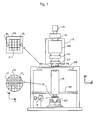
- Figure 1 schematically depicts a lithographic projection apparatus useable in a method according to an embodiment of the invention.
- the apparatus comprises:
- the apparatus is of a transmissive type (e.g. has a transmissive mask). However, in general, it may also be of a reflective type, for example ( e.g. with a reflective mask). Alternatively, the apparatus may employ another kind of patterning device, such as a programmable mirror array of a type as referred to above.
- the source LA e.g. an excimer laser
- This beam is fed into an illumination system (illuminator) IL, either directly or after having traversed conditioning means, such as a beam expander Ex, for example.
- the illuminator IL may comprise adjusting means AM for setting the outer and/or inner radial extent (commonly referred to as ⁇ -outer and ⁇ -inner, respectively) of the intensity distribution in the beam.
- ⁇ -outer and ⁇ -inner commonly referred to as ⁇ -outer and ⁇ -inner, respectively
- it will generally comprise various other components, such as an integrator IN and a condenser CO.
- the beam PB impinging on the mask MA has a desired uniformity and intensity distribution in its cross-section.
- the source LA may be within the housing of the lithographic projection apparatus (as is often the case when the source LA is a mercury lamp, for example), but that it may also be remote from the lithographic projection apparatus, the radiation beam which it produces being led into the apparatus (e.g. with the aid of suitable directing mirrors); this latter scenario is often the case when the source LA is an excimer laser.
- the current invention and claims encompass both of these scenarios.
- the beam PB subsequently intercepts the mask MA, which is held on a mask table MT. Having traversed the mask MA, the beam PB passes through the projection lens PL, which focuses the beam PB onto a target portion C of the substrate W.
- the substrate table WT can be moved accurately, e.g. so as to position different target portions C in the path of the beam PB.
- the first positioning device can be used to position the mask MA accurately with respect to the path of the beam PB, e.g. after mechanical retrieval of the mask MA from a mask library, or during a scan.
- movement of the object tables MT, WT will be realized with the aid of a long-stroke module (coarse positioning) and a short-stroke module (fine positioning), which are not explicitly depicted in Figure 1.
- the mask table MT may just be connected to a short stroke actuator, or may be fixed.
- the depicted apparatus can be used in two different modes:
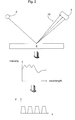
- the scatterometer comprises a broadband (white light) radiation source 2, which directs radiation onto a substrate 6.
- An extended broadband radiation source may be configured to provide the radiation beam with a wavelength of at least 50nm to the substrate surface.
- the reflected radiation is passed to a spectrometer detector 4, which measures a spectrum 10 (intensity as a function of wavelength) of the specular reflected radiation. From this data, the structure or profile giving rise to the detected spectrum may be reconstructed, e.g. by Rigorous Coupled Wave Analysis and non-linear regression or by comparison with a library of simulated spectra as shown at the bottom of Figure 2.
- the general form of the structure is known and some parameters are assumed from knowledge of the process by which the structure was made, leaving only a few parameters of the structure to be determined from the scatterometry data.
- the scatterometer may be a normal-incidence scatterometer or an oblique-incidence scatterometer. Variants of scatterometry may also be used in which the reflection is measured at a range of angles of a single wavelength, rather than the reflection at a single angle of a range of wavelengths.
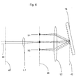
- a scatterometer configured to measuring a property of a substrate by measuring, in a pupil plane 40 of a high NA lens, a property of an angle-resolved spectrum reflected from the substrate surface 6 at a plurality of angles and wavelengths as shown in Figure 3.
- the scatterometer comprises a radiation source 2 configured to project radiation onto the substrate and a detector 32 configured to detect the reflected spectra.
- the pupil plane is the plane in which the radial position of radiation defines the angle of incidence and the angular position defines the azimuth angle of the radiation and any substantially conjugate plane.
- the detector 32 is placed in the pupil plane of the high NA lens.
- the NA is high and, in an embodiment, at least 0.9 or at least 0.95. Immersion scatterometers may even have lenses with an NA over 1.
- Previous angle-resolved scatterometers have only measured the intensity of scattered light.
- An embodiment of the present invention allows several wavelengths to be measured simultaneously at a range of angles.
- the properties measured by the scatterometer for different wavelengths and angles may include the intensity of transverse magnetic (TM) and transverse electric (TE) polarized light and the phase difference between the TM and TE polarized light.
- a broadband light source i.e. one with a wide range of light frequencies or wavelengths ⁇ and therefore of colors
- the plurality of wavelengths in the broadband light in an embodiment, each has a bandwidth of, say, ⁇ and a spacing, therefore, of at least 2 ⁇ ( i.e. twice the wavelength).
- sources can be different portions of an extended radiation source that have been split using, say, fiber bundles. In this way, angle resolved scatter spectra can be measured at multiple wavelengths in parallel.
- a 3-D spectrum (wavelength and two different angles) may be measured, which contains more information than a 2-D spectrum. This allows more information to be measured which increases metrology process robustness.
- a scatterometer of an embodiment of the present invention is shown in Figure 3.
- the light source 2 is focused using lens system L2 through interference filter 30 and is focused onto substrate 6 via a microscope objective lens L1.
- the radiation is then reflected via partially reflective surface 34 into a CCD detector in the back projected pupil plane 40 in order to have the scatter spectrum detected.
- the pupil plane 40 is at the focal length of the lens system L1.
- a detector and high NA lens are placed at the pupil plane.
- the pupil plane may be re-imaged with auxiliary optics since the pupil plane of a high NA lens is usually located inside the lens.
- the pupil plane of the reflector light is imaged on the CCD detector with an integration time of, for example, 40 milliseconds per frame.
- the detector may be, for example, an array of CCD detectors or CMOS detectors.
- the processing of the spectrum gives a symmetrical detection configuration and so sensors can be made rotationally symmetrical. This allows the use of a compact substrate table because a target on the substrate can be measured at any rotational orientation relative to the sensor. All the targets on the substrate can be measured by a combination of a translation and a rotation of the substrate.
- a set of interference filters 30 may be available to select a wavelength of interest in the range of, say, 405 - 790 nm or even lower, such as 200 - 300 nm.
- the interference filter may be tunable rather than comprising a set of different filters.
- a grating could be used instead of one or more interference filters.
- the substrate 6 may be a grating.
- the grating may be printed such that after development, a series of bars are formed of solid resist lines.
- the bars may alternatively be etched into the substrate.
- This pattern is sensitive to comatic aberrations in a lithographic projection apparatus, particularly the projection system PL, and illumination symmetry and the presence of such aberrations will manifest themselves in a variation in the printed grating. Accordingly, the scatterometry data of the printed gratings is used to reconstruct the gratings.
- One or more parameters of the grating, such as line widths and shapes, may be input to the reconstruction process from knowledge of the printing step and/or other scatterometry processes.
- CPBS complex photonic band structures
- Wood-Rayleigh anomalies In transmission metallic gratings with rectangular slits, complex photonic band structures (CPBS) are shown to exhibit strong discontinuities, which are located on Wood-Rayleigh anomalies and reveal two types of resonance, which are referred to as horizontal and vertical surface-plasmon resonances. Spectral position and width of peaks in the spectrum can be directly extracted from CPBS for both horizontal and vertical resonances. In this way, the radiation coming off a transmission metallic grating can have its spectrum analyzed and one or more properties of the grating determined by the strong discontinuities located on the Wood-Rayleigh anomalies. Wood-Rayleigh anomalies occur upon the variation of wavelength or angle of incidence, giving an additional propagating diffraction order. The greater the beam width, the greater the lateral displacement of the beam.
- An embodiment of the present invention detects the spectrum and creates a symmetrical pupil plane image from which the discontinuities can be measured and one or more grating properties therefore calculated.
- the scatterometer may be adapted to measure the overlay of two misaligned periodic structures by measuring asymmetry in the reflected spectrum, the asymmetry being related to the extent of the overlay.
- the scatterometer is adapted to measure the overlay of two misaligned gratings or periodic structures by measuring asymmetry in the reflected spectrum and/or the detection configuration, the asymmetry being related to the extent of the overlay. Thanks to the symmetrical detection configuration, any asymmetry is clearly distinguishable. This provides a straightforward way to measure misalignment in the gratings.
- a grating 14 has a second grating 12 printed on top of it.
- the amount by which the grating 12 is offset with respect to grating 14 is known as the overlay 22.
- the radiation source 2 illuminates the object symmetrically with respect to the surface normal and the scatterometry detector measures scatter radiation from several angles, although a source which illuminates the object from an oblique angle is also possible.
- Overlay metrology is based on the measurement of an asymmetry in the angular scatter spectrum. Symmetric structures yield symmetric angular spectra and an asymmetry in the target shows up as an asymmetry in the angular scatter spectrum. This property is the basis of overlay metrology using angle-resolved scatterometry.
- Two overlapping but misaligned gratings 12 and 14 made of bars with width 20 form one composite asymmetric target.
- the resulting asymmetry in the angular scatter spectrum is detected with the angle-resolved scatterometer 4 shown in Figure 3 and used to derive the overlay 22 in the following manner:
- Two grating pairs are used with a deliberate bias of + d and - d in, respectively, the first and second pair.
- grating 12 is shifted in one direction in one pair (as shown in Fig. 4) and in the opposite direction in the other pair (not shown).
- two grating targets are used; one with the overlay shown in Figure 4b and a second with the exact reverse overlay, so the upper grating 12 is displaced to the left rather than the right with respect to the bottom grating 14.
- the overlay can therefore be calculated using measurements of the asymmetry in the angle resolved scatter spectrum.
- An advantage of this method compared to previously known methods is the fact that only two gratings are required.
- the method can also work for 2-D gratings: in that case only 2 gratings are required for a complete ( x,y ) overlay measurement. This is a significant improvement compared to, say, 6 gratings that spectroscopic scatterometry methods use.
- the coefficients F n,m and G p,q can be interpreted as diffraction efficiencies that depend on the grating shape, wavelength and polarization.
- the two gratings overlap with a relative overlay of x 0 and y 0 in, respectively, the x and y directions.
- this amplitude generally depends on the overlay in the x and y direction. For simplicity, only diffraction orders running in the x -direction are considered. The analysis that follows can also be done for diffraction orders in the y -direction. This would only require an adjustment of variables.
- the overlay is small compared to the pitch of the gratings.
- a 1 x K 0 ( OV x + d ) + K xy ( OV y + d ) ( OV x + d )
- a 1 y K 0 ( OV y + d ) + K xy ( OV y + d ) ( OV x + d )
- a 2 x K 0 ( OV x - d ) + K xy ( OV y - d ) ( OV x + d )
- a 2 y K 0 ( OV y - d ) + K xy ( OV y - d ) ( OV x - d )
- one or more apertures may be provided to the scatterometer to mimic lithography exposure conditions when the grating pattern(s) was created.
- the apertures may then be used in the creation of the angle-resolved spectroscopic image of the grating pattern(s) using the scatterometer.
- the space between the substrate and the detector in liquid, more specifically, the space between lens L1 and the substrate 6 as shown in Figure 3.
- the liquid may be water. This has the advantage of increasing the spatial bandwidth of the medium between the substrate 6 and the lens L1. This means that a diffraction that would be evanescent, for example, in air can propagate and be captured by the lens. With immersion of the space, therefore, it becomes possible to detect a higher diffraction order that contains more detailed information about the grating under investigation than with, for example, air in the space.
- the numerical aperture (NA) of the scatterometer is preferably at least 0.9, even 0.95 or above 1.
- the immersion fluid should have a large index step with respect to, for example, the resist that is on the substrate 6. This may allow maximum contrast in the detector image.
- a possible liquid that fulfils such requirements is water.
- Figure 5 shows, according to an embodiment of the invention, the use of one and the same detector to monitor the source output intensity and the intensity of scattered radiation, which avoids synchronization problems and allows a real-time compensation for source output variations.
- the scatterometer may comprise a non-polarizing beam splitter and a tilted mirror for coupling off a portion of the radiation beam emitted from the radiation source for separate measurement with the same detector.
- the portion of the radiation beam is used to measure the intensity of the radiation beam and the scatterometer may be adapted to compensate for fluctuations in intensity of the radiation beam.
- Advantages of using the same CCD detector for the intensity measurement beam alongside the main measurement beam are that no extra detector is required and so there is no difference in optical and thermal properties between a reference sensor and a metrology sensor; and there are no extra electronics required to trigger, read out and store the reference signal. Any intensity variations may be measured and compensated for.
- a non-polarizing beam splitter 50 in the radiation path images scattered radiation on a two-dimensional detector 32.
- An extra lens re-images the pupil plane onto the CCD detector.
- the intensity incident on the detector is shown as image 36.
- the non-polarizing beam splitter 50 also couples out a portion of the radiation beam to use it for monitoring intensity noise. Instead of measuring this radiation portion with a separate detector, the light is retro-reflected using tilted mirror 52 and transmitted to a separate part of the same detector 32.
- An optional pupil stop 54 limits the extent of the radiation portion and the mirror tilt ensures that the radiation portion is projected alongside the main radiation beam.
- the spectrum is imaged onto the detector 32 at the pupil plane of L1.
- the scatterometer comprises a wavelength multiplexer between the radiation source and the substrate and a demultiplexer between the substrate and the detector. This allows several different wavelengths (or colors) to be measured simultaneously, giving more information in a shorter time frame and therefore robustness as discussed above.
- the wavelength multiplexer may comprise a dispersive element placed at a back-projected object plane or a dispersive element placed at a pupil plane.
- the surface area of the radiation source is preferably split into N parts that are each coupled to a wavelength multiplexer, where N is the number of discrete wavelengths. This splitting can be done, for example, with fiber bundles and the like.
- the multiplexer comprises a dispersive element placed at a back-projected object plane.
- the dispersive element may be a grating or prism adapted to accommodate N discrete wavelengths each with a bandwidth ⁇ and a spacing of at least twice the bandwidth, i.e. 2 ⁇ . This may maximize the usage of an extended light source. Measurement of different wavelengths no longer has to be time-multiplexed because it can be done at the same time, and so a major advantage is that throughput is increased.
- the demultiplexer comprises a dispersive element placed at a pupil plane.
- One or more optical wedges may be inserted in the object plane to achieve well-defined separation of angle-resolved spectra in the pupil plane.
- an extended broadband radiation source such as a xenon, deuterium or quartz tungsten halogen light source is used.
- These sources have a large etendue that gives a surface area that can be split into discrete wavelengths and offer more information as discussed above.
- the wavelengths may be in the range of 193 to 800 nm.
- a dispersive prism or grating which combines N discrete wavelengths is used in the illumination branch (or the radiation path between the source 2 and the substrate 6 in Figure 2) and a grating or prism is used in the detection branch (or the space between the radiation path between the substrate 6 and the detector 4) to spatially separate the wavelengths.
- FIG. 6 An example of a multiplexing grating is shown in Figure 6.
- Two light sources S 1 and S2 are transmitted through a lens system L2 and strike a Littrow mounted grating 16 which is in the object plane 42 and are focused on the pupil plane 40 before being transmitted through a lens system L1 to another object plane 42 and optionally into an illumination fiber 60.
- the pupil plane contains rectangular apertures of suitable dimensions - the width determining the angular extent of the light incident on the grating. This angular extent and the grating pitch determine the bandwidth of the returning light that is transmitted via the aperture in the pupil plane.
- a grating with 1200 lines per millimeter yields a dispersion of approximately 1.2 mrad/nm.
- An effective bandwidth of 4 nm corresponds to a full angular width of the illumination beam of 3.33 mrad.
- the spot size of the substrate 6 is approximately 40 ⁇ m and its NA is 0.95.
- the beam diameter on the grating is therefore approximately 23 mm. If the focal length of the lens L1 is 100 mm, then the width of the aperture holes in the pupil plane must be 333 ⁇ m. If an illumination fiber is used, then the illumination NA must be approximately 0.22.
- more than two radiation sources may be used at a time.
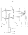
- FIG. 7 shows an example of a wavelength demultiplexer in the detection branch. For simplicity, the separation of only two wavelengths is again shown.
- the demultiplexer is similar to the muliplexer, except that the grating is placed in the pupil plane and not in the object plane.
- the light that is diffracted by the grating in the Littrow mounted grating 16 is transmitted by the lens L2, which makes two object images with wavelengths ⁇ 1 and ⁇ 2 in the object plane.
- Each hole of the field stop 40 also has a wedge 62 with a unique wedge angle. This wedge 62 ensures that the angle resolved scatter spectrum for each wavelength is imaged on a different part of the CCD detector 32.
- the CCD detector is based at the second pupil plane 40.
- the wedges 62 can deflect the light in two directions, it is possible to realize an efficient filling of a CCD detector with many angle resolved spectra.
- the targets should be well focused.
- the pupil plane 40 of a high NA objective is imaged on a detector with a double telecentric system as shown in Figure 8 according to an embodiment of the invention.
- the NA is high; preferably at least 0.9.
- a knife edge 70 in the intermediate object plane 42 blocks one half of the intermediate object image.
- the edge may be a Foucault knife-edge.
- the knife-edge helps to focus the image of the radiation onto the substrate.
- the intensity in the outer regions (or practically speaking, in two halves) of the pupil plane 40 is sampled.
- a difference in intensities I1 and I2 is produced.
- the proportionality factor k is independent of the image and needs to be determined only once, though since the focus sensor can be used in an integrating feedback loop, the precise value of k is not important.
- Illumination sources are not always homogeneous and must be calibrated and corrected for in order to guarantee precise exposure of the substrates. Inhomogeneity may be caused by the illumination sources themselves, or by the roughness of surface coatings of reflectors in the illumination path.
- normalization of the illumination beam has been done using an aluminium mirror. However, this normalization fails when the object to be measured (i.e. gratings or the substrate) generate higher diffraction orders. These cause tool induced shift errors in overlay applications.
- the scatterometry system further comprises one or more mirrors in the illumination beam.
- the mirrors may be a fiducial on the substrate table and may be made of aluminium. These mirrors either tilt or exist at different tilt angles in order to create at least two images reflected in different angles. For each tilt angle, the detected spectrum shifts in the same direction as the direction of the tilt. These images are detected and combined into differential equation, from which the illumination profile of the radiation beam may be determined. The resultant illumination profile is used to correct measurements of the property of the reflected spectrum at higher diffraction orders.
- M 0 (k) [ A ( - k ) R 0 ( k ) + A ( - k ⁇ k G ) R ⁇ 1 ( x ) + ⁇ ⁇ ⁇ + A ( - k ⁇ Nk G ) R ⁇ N ( x ) ] B ( k ) where:
- the mirror may be a single convex or concave mirror, or it may be a plane mirror that is actively tilted over a range of angles during detection. Alternatively, there may be a range of mirrors at different tilt angles.
- the measured reflection angle may be in a radial direction (this alters the magnitude of the tilt) or in an azimuthal direction (this alters the direction of the tilt).
- ⁇ is the shift in the pupil plane, which generally depends on the position k in the pupil plane.
- ⁇ ( k ) 2 ⁇ M 1 - k 2
- a plane mirror may be employed that is mechanically tilted using actuators.
- a more elegant and simple approach is the use of a concave or convex mirror with a radius of curvature R and lateral position x.
- a concave or convex spherical aluminum fiducial on the substrate stage therefore renders the calibration straightforward because the proper tilt is simply achieved by moving the fiducial to the proper location under the detector.
- An embodiment of the invention uses a radiation beam with an annular intensity distribution in a conjugate plane to the substrate.
- the radiation source may comprise mechanical blades, spatial light modulators or spatially coherent broadband lasers and a zoom-axicon (i.e. to create a ring of laser light).
- the annular radiation beam preferably comprises small- ⁇ illumination.
- annular radiation has advantages over, say, inserting a blade, because there is no light loss because almost all the photons are "used". This is particularly important where light sources such as UV or DUV are used because they emit fewer photons than more abundant light sources and so losing a number of those photons is more noticeable. In particular, this is noticeable in signal collection because the lithographic tool suffers a certain amount of delay if there is a lower light intensity.
- Annular light sources have the further advantage of not causing internal reflections as blades might. Internal reflections require blocking to avoid light artefacts. Of course, other illumination techniques, such as quadrupole illumination, which offer the same advantages may be used.
- the annulus of the annular radiation is placed in the pupil plane of the high NA lens.
- the pupil plane is not directly accessible and in practice, the annulus is placed in a back-projected image of the pupil plane in the illumination branch of the scatterometer.
- the advantage of annular illumination is that the intensity of the +1/-1 diffraction order of a grating with a small pitch of the order of ⁇ /NA may be separately measured.
- This embodiment may be used for calculating variations in substrate tilt by putting a shaped obscuration in the radiation beam and detecting changes in the width and shape of the shaped obscuration on the substrate caused by variations in the substrate tilt.
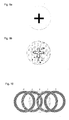
- the shaped obscuration may be, for example, a cross-hair as shown in Figures 9a and 9b. It may, of course, be any other shape and it does not have to be in the centre of the pupil plane.
- the idea of measuring wafer tilt is based on the fundamental relation that a tilt in the wafer plane causes a shift in the pupil plane.
- a cross-haired obscuration is placed in the center of the illumination beam. This produces a black cross-hair in the scattered light in the pupil plane as shown in Figure 9a.
- this cross will vary if the substrate tilt changes. As a result, the difference may be measured between this pattern (at zero tilt) and an actual measurement at an unknown tilt to obtain an image as shown in Figure 9b.
- a small tilt in the substrate does not lead to a substantial shape change in the annulus of light, but rather, it will lead to a shift of the pupil plane image. This shift is generally small and of the order of 0.1 pixels.
- the values between pixels may be interpolated by curve fitting, for example. By fitting a curve through the dark-light transition that occurs at the edge of the annulus, sub-pixel displacements of the annulus may be measured. The width and sign of these transitions can be used to calculate and correct for the substrate tilt in 2 dimensions. In this way the substrate can be measured at constant (zero) tilt.
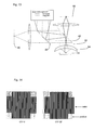
- Figure 10 shows the diffraction orders of small pitched gratings detected using radiation with an annular intensity distribution in a conjugate plane to the substrate.
- annular intensity distribution allows the shape of the images as shown in Figure 10 and thereby allows clearer and more precise measurement of substrate tilt.
- the image labelled 0 is the central zero-order diffraction order as imaged in the detector.
- the images labelled -2, -1, 1 and 2 are higher diffraction orders. These higher diffraction orders are shifted with respect to the lower diffraction order and so are easier to measure for overlay metrology of isolated 1-D and 2-D features.
- a coarse grid may be measured and a pixel interpolation technique used to interpolate the overall shape at the pupil plane.
- An annular beam is more advantageous in this case, too, because there are areas in the pupil plane that only receive light from first order diffraction. If a block beam were used, for instance, each point in the pupil plane would receive light from either the zeroth order or a combination of the zeroth order and the first order, causing errors in the measurement at the pupil plane.
- Normal measurements using a scatterometer involve measuring the properties of a single target on a single substrate with a single polarization at one time.
- An embodiment of the invention uses illumination source to project a plurality of illumination spots onto a substrate.
- the detector of the scatterometer simultaneously detects an angle-resolved spectrum of the plurality of illumination spots reflected from a surface of the substrate.
- the plurality of illumination spots may be created using a double illumination fiber or a Wollaston prism for creating two orthogonally polarized illumination spots.
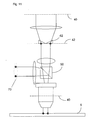
- Figure 11 shows part of the scatterometer hardware.
- Two illumination spots 70 are split in beam splitter 50 before being transmitted down through the high numerical aperture objective positioned in the pupil plane 40 onto the substrate 6.
- the reflected beam is transmitted upwards through two wedges 62 that separate the two angle resolved spectra in the pupil plane, the wedges themselves being positioned in the intermediate image plane 42.
- the illumination beams are then detected by the CCD on the re-imaged pupil plane 40 at the top of Figure 11.
- Two, or even more, parallel measurements may thereby be made; for example, of horizontal and vertical lines for a single polarization; or even for both horizontal and vertical lines for both TE and TM polarization.
- the illumination branch further includes a first polarizer configured to linearly polarize the radiation beam; a beam splitter configured to split the radiation beam into two orthogonal components (E TE , E TH ); a second polarizer configured to polarize the scattered beam; a variable compensator (a Pockells Cell, Wollaston prism pair or Soleil-Babinet compensator) positioned between the first and second polarizers, the variable compensator being configured to vary the optical path difference between orthogonally polarized components (and optionally between the beam splitter and the high numerical aperture lens); and a 2-dimensional detector for detecting sinusoidal intensity variation of the resultant beam components.
- the compensator is most commonly in the main illumination branch of the scatterometer, though it may of course be in a second illumination branch.
- the 2-dimensional detector such as a Complementary Metal Oxide Semiconductor detector (CMOS) has a high frame rate, i.e. in the region of 1000 frames per second.
- Figure 12 shows how the angular-resolved spectroscopic concept is turned into an angle-resolved spectroscopic ellipsometer.
- An illumination beam with two wavelengths, ⁇ 1 and ⁇ 2 ; and illumination profiles ⁇ , and ⁇ 2 is transmitted through a 45° polarizer 72, reflected off the substrate 6 and transmitted through a variable compensator 74 before being polarized again.
- the illumination beam is divided into two beams with a phase difference ⁇ between the TE and TM polarized beams.
- the grid 36 in Figure 12 shows the 2-D detector array and the time-dependent intensity variation in one pixel of this array. The other pixels will show a comparable variation.
- the beams are passed through two bandpass filters 76 to obtain the illumination profiles of ⁇ 1 and ⁇ 2 .
- the resultant ellipsometric parameters cos( ⁇ ), sin( ⁇ ) and tan( ⁇ ) are virtually insensitive to internal sensor scattering and so the signal to noise ratio can be improved.
- the operation is modeled with Jones vectors and matrices below, though it could also be modeled using Mueller matrices, which enable the inclusion of imperfections of the optical components in the mathematical models.
- tan( ⁇ ) and cos( ⁇ ) are the signals that are measured and simulated to obtain the profile information. In that case, tan( ⁇ ) and cos( ⁇ ) are recorded as a function of wavelength. In the present invention, tan( ⁇ ) and cos( ⁇ ) are obtained as a function of position in the pupil plane and can be used for similar analyses.
- the ellipsometric parameters are used to measure layer thickness by solving an inverse scattering problem, i.e. the measured parameters are compared with modeled parameters and the stack parameters are determined by minimizing the root-mean-square difference (or any other suitable metric) between the measured and modeled parameters.
- the various wavelengths can be separated with a bandpass filter. This can be easily realized via signal processing with, for example, discrete Fourier Transform techniques.
- the compensator can also be place in the illumination branch. Moreover, it can also be placed between the beam splitter and a high numerical aperture objective. This has the advantage that the OPD variation is doubled.
- the 2-D detector is the critical part of this concept; to ensure sufficiently short measurement times, it must have a high frame rate.
- CMOS detectors can achieve very high frame rates, for example 1000 frames per second.
- Measuring overlay as described in paragraphs 51 to 80 above does not allow for the measurement of large overlay errors, in particular, overlay errors equal to an integer times the grating pitch.
- the ability to detect overlay errors smaller than the grating pitch is of no use if there is an overlay error that means the grating lines are lined up with each other, but shifted by several grating pitch widths.
- An embodiment of the invention therefore uses the second detector branch already present in the scatterometer (and discussed above) for carrying out coarse overlay measurements to determine whether coarse errors exist, such as whether the grating overlay error is in fact greater than the pitch of the grating.
- a coarse overlay measurement is an imaging-based technique, wherein a second camera looks at an image of two overlapping gratings and determines whether there are large displacements by comparing the positions of the edges of markers on a substrate.
- a perfect overlay will have perfectly aligned marker edges.
- Pattern recognition algorithms are used to determine the edge of a grating in the process layer and the edge of the grating in the resist layer. This measurement is done on the four sides or corners of a grating pair. The measured edge positions are used to calculate the position of the resist grating relative to the position of the grating in the process layer.
- the scatterometer of the present invention allows a very simple solution.
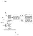
- the scatterometer comprises a separate imaging branch that images the substrate surface on a CCD camera. This second camera branch is needed for measuring the position of the substrate through an alignment and pattern recognition step.
- the second branch is shown schematically in Figure 13.
- the pupil plane 40 measurement (the actual angle resolved measurement) requires an illumination source that underfills the target at the object plane 42 (i.e. the measurement spot is smaller than the measurement target).
- the pupil plane imaging illumination beams are shown as solid lines in Figure 13. In this case, only a portion of the target is measured and structures outside the target area are not illuminated. If the measurement spot fills or overfills the measurement target, the measurement signal is disturbed by the area surrounding the target and data interpretation and signal analysis are unnecessarily complicated.
- the image plane measurement on the other hand, must overfill the target in order to detect the alignment because the complete pupil plane must be sampled, including the contours of the target.
- the light rays for the image plane measurements are shown as dashed lines.
- the image of the object plane is formed on a first CCD camera 80 and the image of the pupil plane is formed on a second CCD camera 82.
- Figure 14 shows one possible example of an overlay target for zero overlay (lefthand drawing) and an X-overlay equal to twice the grating pitch (right-hand drawing).
- the pupil plane measurement would yield the same measured overlay of zero for both situations making it an unreliable measurement.
- the image plane measurement can clearly distinguish between these two situations. In this way, a robust two-stage metrology scheme may be carried out as follows:
- the 200 nm criterion is an indicative example. It may be made to any sensible threshold. Assuming that the image plane CCD has 1000 ⁇ 1000 pixels and assuming a pixel pitch of 100 nm at substrate level, the total field of view will be 100 ⁇ 100 ⁇ m 2 , which is adequate for pattern recognition and alignment while still allowing coarse overlay measurements with an accuracy of the order of 20-50 nm.
- Coarse overlay can only be measured when the entire alignment marker is visible to the CCD. If, for example, only the centre part of the marker is visible, the substrate table needs to be moved to the edge of the marker to enable the measurement of the coarse overlay. This calls for additional movement of the table, thereby slowing the measurement taking process.
- a larger field of view allows the capture of the marker in one "stroke" and a coarse measurement to be carried out quickly while a second camera is free to capture the image on the pupil plane and obtain the detailed overlay information.
- the field of view that is required for capturing the relevant image can be reduced even further if the results of edge pre-alignment and coarse wafer align in the exposure tool are used. With these data, it is possible to predict the location of the markers on the substrate with ⁇ m accuracy after the edge pre-alignment in the overlay metrology module is complete.
- An embodiment of the invention detects not just overlay errors, but also damaged gratings using the scatterometer arranged for CD metrology on gratings or other periodic structures.
- the scatterometer normally detects specular light; i.e. lowest order light that has been reflected directly off the grating. Local distortions in the grating destroy the periodicity of the grating and result in scattering in a non-specular direction.
- the scatterometer can be used to detect an angle-resolved spectrum of the scattered beam at various angles outside its specular direction. Radiation with an annular intensity distribution, or small- ⁇ illumination, may be used for greater accuracy and images that easier to read.
- An embodiment of the invention may be used for detecting bubble defects in an immersion lithographic apparatus, where a liquid is introduced between the projection system and the substrate as discussed above.
- bubble defects have been measured using off-line defect inspection tools.
- Off-line tools take a longer time to produce results than on-line tools because substrates must be taken out of the production line and queued.
- Bubbles in the liquid cause a surface imperfection on the substrate, which will cause light scattering when the surface is exposed to light. This scattered radiation is measured using the scatterometer of the invention and the cause of the scattering extrapolated back to bubble defects.
Landscapes
- Physics & Mathematics (AREA)
- General Physics & Mathematics (AREA)
- Health & Medical Sciences (AREA)
- Life Sciences & Earth Sciences (AREA)
- Chemical & Material Sciences (AREA)
- Analytical Chemistry (AREA)
- Biochemistry (AREA)
- General Health & Medical Sciences (AREA)
- Immunology (AREA)
- Pathology (AREA)
- Engineering & Computer Science (AREA)
- Condensed Matter Physics & Semiconductors (AREA)
- Manufacturing & Machinery (AREA)
- Computer Hardware Design (AREA)
- Microelectronics & Electronic Packaging (AREA)
- Power Engineering (AREA)
- Exposure And Positioning Against Photoresist Photosensitive Materials (AREA)
- Investigating Or Analysing Materials By Optical Means (AREA)
- Length Measuring Devices By Optical Means (AREA)
- Investigating Materials By The Use Of Optical Means Adapted For Particular Applications (AREA)
- Exposure Of Semiconductors, Excluding Electron Or Ion Beam Exposure (AREA)
Priority Applications (1)
| Application Number | Priority Date | Filing Date | Title |
|---|---|---|---|
| EP10170874.1A EP2239632B1 (de) | 2004-08-16 | 2005-08-11 | Vorrichtung zum Berechnen von Variationen der Substratneigung |
Applications Claiming Priority (1)
| Application Number | Priority Date | Filing Date | Title |
|---|---|---|---|
| US10/918,742 US7791727B2 (en) | 2004-08-16 | 2004-08-16 | Method and apparatus for angular-resolved spectroscopic lithography characterization |
Related Child Applications (2)
| Application Number | Title | Priority Date | Filing Date |
|---|---|---|---|
| EP10170874.1A Division EP2239632B1 (de) | 2004-08-16 | 2005-08-11 | Vorrichtung zum Berechnen von Variationen der Substratneigung |
| EP10170874.1 Division-Into | 2010-07-27 |
Publications (3)
| Publication Number | Publication Date |
|---|---|
| EP1628164A2 true EP1628164A2 (de) | 2006-02-22 |
| EP1628164A3 EP1628164A3 (de) | 2006-04-12 |
| EP1628164B1 EP1628164B1 (de) | 2010-10-06 |
Family
ID=35197995
Family Applications (2)
| Application Number | Title | Priority Date | Filing Date |
|---|---|---|---|
| EP05254994A Active EP1628164B1 (de) | 2004-08-16 | 2005-08-11 | Verfahren und Vorrichtung zur Charakterisierung der Lithographie mittels winkelaufgelöster Spektroskopie |
| EP10170874.1A Active EP2239632B1 (de) | 2004-08-16 | 2005-08-11 | Vorrichtung zum Berechnen von Variationen der Substratneigung |
Family Applications After (1)
| Application Number | Title | Priority Date | Filing Date |
|---|---|---|---|
| EP10170874.1A Active EP2239632B1 (de) | 2004-08-16 | 2005-08-11 | Vorrichtung zum Berechnen von Variationen der Substratneigung |
Country Status (8)
| Country | Link |
|---|---|
| US (8) | US7791727B2 (de) |
| EP (2) | EP1628164B1 (de) |
| JP (2) | JP4357464B2 (de) |
| KR (1) | KR100697277B1 (de) |
| CN (1) | CN1916603B (de) |
| DE (1) | DE602005023946D1 (de) |
| SG (4) | SG120263A1 (de) |
| TW (1) | TWI294518B (de) |
Cited By (430)
| Publication number | Priority date | Publication date | Assignee | Title |
|---|---|---|---|---|
| WO2006091783A1 (en) * | 2005-02-25 | 2006-08-31 | Accent Optical Technologies, Inc. | Apparatus and method for enhanced critical dimension scatterometry |
| EP1870696A1 (de) * | 2006-06-22 | 2007-12-26 | ASML Netherlands B.V. | Verfahren und Vorrichtung zur Charakterisierung von winkelaufgelöster spektroskopischer Lithografie |
| WO2008015230A1 (fr) * | 2006-08-02 | 2008-02-07 | Commissariat A L'energie Atomique | Dispositif de caracterisation d'objets uniques |
| DE102006034776B3 (de) * | 2006-07-27 | 2008-03-06 | Infineon Technologies Ag | Verfahren und Messvorrichtung zur ellipsometrischen Vermessung von Strukturelementen sowie Verwendung des Verfahrens |
| US7352439B2 (en) | 2006-08-02 | 2008-04-01 | Asml Netherlands B.V. | Lithography system, control system and device manufacturing method |
| EP1930774A1 (de) | 2006-12-08 | 2008-06-11 | ASML Netherlands B.V. | Streustrahlungsmessgerät und Fokusanalyseverfahren |
| EP2053349A2 (de) | 2007-10-25 | 2009-04-29 | ASML Netherlands B.V. | Verfahren und Vorrichtung zur Ermittlung von Eigenschaften einer lithographischen Struktur auf einem Substrat |
| WO2009071207A1 (en) * | 2007-12-05 | 2009-06-11 | Asml Netherlands B.V. | Inspection apparatus, lithographic apparatus and method of measuring a property of a substrate |
| WO2009078708A1 (en) * | 2007-12-17 | 2009-06-25 | Asml Netherlands B.V. | Diffraction based overlay metrology tool and method |
| US7564555B2 (en) | 2006-08-15 | 2009-07-21 | Asml Netherlands B.V. | Method and apparatus for angular-resolved spectroscopic lithography characterization |
| US7573584B2 (en) | 2006-09-25 | 2009-08-11 | Asml Netherlands B.V. | Method and apparatus for angular-resolved spectroscopic lithography characterization |
| WO2009100867A1 (en) * | 2008-02-13 | 2009-08-20 | Asml Netherlands B.V. | Method and appartus for angular-resolved spectroscopic lithography characterization |
| US7589832B2 (en) | 2006-08-10 | 2009-09-15 | Asml Netherlands B.V. | Inspection method and apparatus, lithographic apparatus, lithographic processing cell and device method |
| WO2009115342A1 (en) * | 2008-03-20 | 2009-09-24 | Asml Netherlands B.V. | Inspection apparatus for lithography |
| WO2009118113A1 (en) * | 2008-03-26 | 2009-10-01 | Asml Netherlands B.V. | Inspection apparatus, lithographic apparatus and method of measuring a property of a substrate |
| US7599064B2 (en) | 2007-03-07 | 2009-10-06 | Asml Netherlands B.V. | Inspection method and apparatus, lithographic apparatus, lithographic processing cell and device manufacturing method, substrate for use in the methods |
| WO2009124669A1 (en) * | 2008-04-09 | 2009-10-15 | Asml Netherlands B.V. | A method of assessing a model of a substrate, an inspection apparatus and a lithographic apparatus |
| US7605907B2 (en) | 2007-03-27 | 2009-10-20 | Asml Netherlands B.V. | Method of forming a substrate for use in calibrating a metrology tool, calibration substrate and metrology tool calibration method |
| WO2009127355A1 (en) * | 2008-04-15 | 2009-10-22 | Asml Netherlands B.V. | Inspection apparatus for lithography |
| WO2009129974A1 (en) * | 2008-04-21 | 2009-10-29 | Asml Netherlands B.V. | Apparatus and method of measuring a property of a substrate |
| WO2009138162A1 (en) * | 2008-05-12 | 2009-11-19 | Asml Netherlands B.V. | Inspection apparatus for lithography |
| US7630087B2 (en) | 2006-11-22 | 2009-12-08 | Asml Netherlands B.V. | Inspection method and apparatus, lithographic apparatus, lithographic processing cell and device manufacturing method |
| WO2009150089A1 (en) * | 2008-06-11 | 2009-12-17 | Asml Netherlands B.V. | Apparatus and method for inspecting a substrate |
| US7643666B2 (en) | 2006-08-08 | 2010-01-05 | Asml Netherlands B.V. | Method and apparatus for angular-resolved spectroscopic lithography characterization |
| US7656518B2 (en) | 2007-03-30 | 2010-02-02 | Asml Netherlands B.V. | Method of measuring asymmetry in a scatterometer, a method of measuring an overlay error in a substrate and a metrology apparatus |
| WO2010020506A1 (en) * | 2008-08-21 | 2010-02-25 | Asml Netherlands B.V. | Inspection method and apparatus, and lithographic apparatus |
| US7701577B2 (en) | 2007-02-21 | 2010-04-20 | Asml Netherlands B.V. | Inspection method and apparatus, lithographic apparatus, lithographic processing cell and device manufacturing method |
| CN101109903B (zh) * | 2006-07-18 | 2010-05-12 | 上海华虹Nec电子有限公司 | 在线监控透镜散光的方法 |
| US7724370B2 (en) | 2007-03-01 | 2010-05-25 | Asml Netherlands B.V. | Method of inspection, a method of manufacturing, an inspection apparatus, a substrate, a mask, a lithography apparatus and a lithographic cell |
| US7738103B2 (en) | 2007-11-08 | 2010-06-15 | Asml Netherlands B.V. | Inspection method and apparatus, lithographic apparatus, lithographic processing cell and device manufacturing method for determining a parameter of a target pattern |
| WO2010076254A1 (en) | 2008-12-30 | 2010-07-08 | Asml Netherlands B.V. | Method of determining a characteristic |
| EP2219078A1 (de) | 2009-02-11 | 2010-08-18 | ASML Netherlands BV | Inspektionsgerät für die Lithographie |
| WO2010115686A1 (en) | 2009-04-07 | 2010-10-14 | Asml Netherlands B.V. | Method and apparatus for inspection in lithography |
| WO2010130516A1 (en) | 2009-05-11 | 2010-11-18 | Asml Netherlands B.V. | Method of determining overlay error |
| US7869022B2 (en) | 2007-07-18 | 2011-01-11 | Asml Netherlands B.V. | Inspection method and apparatus lithographic apparatus, lithographic processing cell, device manufacturing method and distance measuring system |
| WO2011012624A1 (en) | 2009-07-31 | 2011-02-03 | Asml Netherlands B.V. | Metrology method and apparatus, lithographic system, and lithographic processing cell |
| WO2011012412A1 (en) | 2009-07-30 | 2011-02-03 | Asml Netherlands B.V. | Inspection method for lithography |
| US7916284B2 (en) | 2006-07-18 | 2011-03-29 | Asml Netherlands B.V. | Inspection method and apparatus, lithographic apparatus, lithographic processing cell and device manufacturing method |
| EP2302360A2 (de) | 2009-09-24 | 2011-03-30 | ASML Netherlands B.V. | Verfahren und Vorrichtung zur Simulation elektromagnetischer Streuungseigenschaften mikroskopischer Strukturen und Verfahren und Vorrichtung zur Rekonstruktion mikroskopischer Strukturen |
| WO2011045125A1 (en) | 2009-10-13 | 2011-04-21 | Asml Netherlands B.V. | Inspection method and apparatus |
| WO2011045132A1 (en) | 2009-10-12 | 2011-04-21 | Asml Netherlands B.V. | Method, inspection apparatus and substrate for determining an approximate structure of an object on the substrate |
| WO2011048008A1 (en) | 2009-10-22 | 2011-04-28 | Asml Netherlands B.V. | Methods and apparatus for calculating electromagnetic scattering properties of a structure using a normal-vector field and for reconstruction of approximate structures |
| WO2011101192A1 (en) | 2010-02-17 | 2011-08-25 | Asml Netherlands B.V. | Estimating substrate model parameters for lithographic apparatus control |
| WO2011101187A1 (en) | 2010-02-19 | 2011-08-25 | Asml Netherlands B.V. | Lithographic apparatus and device manufacturing method |
| WO2011101184A1 (en) | 2010-02-19 | 2011-08-25 | Asml Netherlands B.V. | Lithographic apparatus and method of producing a reference substrate |
| EP2392970A2 (de) | 2010-02-19 | 2011-12-07 | ASML Netherlands BV | Verfahren und Vorrichtung zur Steuerung eines lithografischen Gerätes |
| WO2011151121A1 (en) | 2010-06-04 | 2011-12-08 | Asml Netherlands B.V. | Measurement of a structure on a substrate |
| WO2012010458A1 (en) | 2010-07-19 | 2012-01-26 | Asml Netherlands B.V. | Method and apparatus for determining an overlay error |
| WO2012048156A2 (en) | 2010-10-08 | 2012-04-12 | Tokyo Electron Limited | Method of determining an asymmetric property of a structure |
| US8189195B2 (en) | 2007-05-09 | 2012-05-29 | Asml Netherlands B.V. | Inspection method and apparatus, lithographic apparatus, lithographic processing cell and device manufacturing method |
| US8223347B2 (en) | 2009-07-06 | 2012-07-17 | Asml Netherlands B.V. | Inspection method and apparatus, lithographic apparatus, lithographic processing cell and device manufacturing method |
| US8233155B2 (en) | 2006-10-13 | 2012-07-31 | Asml Netherlands B.V. | Inspection method and apparatus, lithographic apparatus, lithographic processing cell and device manufacturing method |
| US8237914B2 (en) | 2006-12-01 | 2012-08-07 | Asml Netherlands B.V. | Process, apparatus, and device for determining intra-field correction to correct overlay errors between overlapping patterns |
| US8248579B2 (en) | 2006-12-01 | 2012-08-21 | Asml Netherlands B.V. | Lithographic apparatus, device manufacturing method and device for correcting overlay errors between overlapping patterns |
| US8294907B2 (en) | 2006-10-13 | 2012-10-23 | Asml Netherlands B.V. | Inspection method and apparatus, lithographic apparatus, lithographic processing cell and device manufacturing method |
| EP2515168A2 (de) | 2011-03-23 | 2012-10-24 | ASML Netherlands B.V. | Verfahren und Vorrichtung zur Berechnung elektromagnetischer Streuungseigenschaften von Strukturen und für die Rekonstruktion von approximativen Strukturen |
| WO2012171687A1 (en) | 2011-06-14 | 2012-12-20 | Asml Netherlands B.V. | Inspection for lithography |
| WO2012175253A1 (en) | 2011-06-21 | 2012-12-27 | Asml Netherlands B.V. | Inspection method and apparatus |
| US8411254B2 (en) | 2008-09-02 | 2013-04-02 | Asml Netherlands B.V. | Device manufacturing method, control system, computer program and computer-readable medium |
| EP2579100A2 (de) | 2011-10-03 | 2013-04-10 | ASML Holding N.V. | Inspektionsgerät, lithografisches Gerät und Verfahren zur Herstellung von Bauelementen |
| US8441639B2 (en) | 2009-09-03 | 2013-05-14 | Kla-Tencor Corp. | Metrology systems and methods |
| WO2013079270A1 (en) | 2011-11-30 | 2013-06-06 | Asml Netherlands B.V. | Inspection method and apparatus, and corresponding lithographic apparatus |
| WO2013087431A2 (en) | 2011-12-12 | 2013-06-20 | Asml Netherlands B.V. | Device manufacturing method and associated lithographic apparatus, inspection apparatus, and lithographic processing cell |
| WO2013092106A1 (en) | 2011-12-23 | 2013-06-27 | Asml Netherlands B.V. | Methods and apparatus for measuring a property of a substrate |
| US8497975B2 (en) | 2009-06-11 | 2013-07-30 | Asml Netherlands B.V. | Inspection method and apparatus, lithographic apparatus, lithographic processing cell and device manufacturing method |
| US8502955B2 (en) | 2008-12-30 | 2013-08-06 | Asml Netherlands B.V. | Method of determining a characteristic |
| US8520212B2 (en) | 2008-07-18 | 2013-08-27 | Asml Netherlands B.V. | Scatterometry method and measurement system for lithography |
| US8553218B2 (en) | 2009-12-28 | 2013-10-08 | Asml Netherlands B.V. | Calibration method and apparatus |
| US8553227B2 (en) | 2007-11-13 | 2013-10-08 | Asml Netherlands B.V. | Inspection method and apparatus, lithographic apparatus, lithographic processing cell and device manufacturing method |
| WO2014016056A1 (en) | 2012-07-23 | 2014-01-30 | Asml Netherlands B.V. | Inspection method and apparatus, lithographic system and device manufacturing method |
| US8645109B2 (en) | 2009-12-08 | 2014-02-04 | Asml Netherlands B.V. | Methods and apparatus for determining electromagnetic scattering properties and structural parameters of periodic structures |
| US8685626B2 (en) | 2009-03-04 | 2014-04-01 | Asml Netherlands B.V. | Method of measuring a characteristic |
| US8692994B2 (en) | 2010-03-18 | 2014-04-08 | Asml Netherlands B.V. | Inspection method and apparatus, and associated computer readable product |
| WO2014082813A2 (en) | 2012-11-30 | 2014-06-05 | Asml Netherlands B.V. | Method and apparatus for determining lithographic quality of a structure |
| US8749786B2 (en) | 2009-12-08 | 2014-06-10 | Asml Netherlands B.V. | Inspection method and apparatus, and corresponding lithographic apparatus |
| US8760623B2 (en) | 2007-12-05 | 2014-06-24 | Asml Netherlands B.V. | Inspection apparatus for lithography |
| WO2013124131A3 (en) * | 2012-02-21 | 2014-06-26 | Asml Netherlands B.V. | Inspection apparatus and method |
| US8767183B2 (en) | 2009-06-17 | 2014-07-01 | Asml Netherlands B.V. | Method of overlay measurement, lithographic apparatus, inspection apparatus, processing apparatus and lithographic processing cell |
| US8773640B2 (en) | 2008-05-29 | 2014-07-08 | Asml Netherlands B.V. | Inspection method and apparatus |
| US8793099B2 (en) | 2010-02-19 | 2014-07-29 | Asml Netherlands B.V. | Calibration of lithographic apparatus |
| US8792096B2 (en) | 2008-03-24 | 2014-07-29 | Asml Netherlands B.V. | Inspection apparatus for lithography |
| US8797509B2 (en) | 2008-05-29 | 2014-08-05 | Asml Netherlands B.V. | Inspection method and apparatus, lithographic apparatus, lithographic processing cell and device manufacturing method |
| TWI448829B (zh) * | 2010-02-19 | 2014-08-11 | Asml Netherlands Bv | 微影裝置及圖案化方法 |
| US8823922B2 (en) | 2008-06-26 | 2014-09-02 | Asml Netherlands B.V. | Overlay measurement apparatus, lithographic apparatus and device manufacturing method using such overlay measurement apparatus |
| US8830447B2 (en) | 2009-05-12 | 2014-09-09 | Asml Netherlands B.V. | Inspection method for lithography |
| US8848195B2 (en) | 2008-10-31 | 2014-09-30 | Asml Netherlands B.V. | Inspection method and apparatus, lithographic apparatus, lithographic processing cell and device manufacturing method for determining a property of a substrate |
| US8868387B2 (en) | 2007-10-09 | 2014-10-21 | Asml Netherlands B.V. | Method of optimizing a model, a method of measuring a property, a device manufacturing method, a spectrometer and a lithographic apparatus |
| US8875078B2 (en) | 2011-08-03 | 2014-10-28 | Asml Netherlands B.V. | Reference library generation method for methods of inspection, inspection apparatus and lithographic apparatus |
| US8876346B2 (en) | 2011-07-28 | 2014-11-04 | Asml Netherlands B.V. | Illumination source for use in inspection methods and/or lithography; inspection and lithographic apparatus and inspection method |
| US8887107B2 (en) | 2012-09-06 | 2014-11-11 | Asml Netherlands B.V. | Inspection method and apparatus and lithographic processing cell |
| US8885150B2 (en) | 2008-02-27 | 2014-11-11 | Asml Netherlands B.V. | Inspection method and apparatus, lithographic apparatus, lithographic processing cell and device manufacturing method |
| US8891061B2 (en) | 2008-10-06 | 2014-11-18 | Asml Netherlands B.V. | Lithographic focus and dose measurement using a 2-D target |
| US8922755B2 (en) | 2008-04-29 | 2014-12-30 | Asml Netherlands B.V. | Support structure, inspection apparatus, lithographic apparatus and methods for loading and unloading substrates |
| US8947630B2 (en) | 2010-02-19 | 2015-02-03 | Asml Netherlands B.V. | Lithographic apparatus and device manufacturing method |
| US8972031B2 (en) | 2010-03-19 | 2015-03-03 | Asml Netherlands B.V. | Control method and apparatus |
| US8982329B2 (en) | 2008-04-24 | 2015-03-17 | Asml Netherlands B.V. | Method and apparatus for measuring line end shortening, substrate and patterning device |
| US8994921B2 (en) | 2008-11-07 | 2015-03-31 | Asml Netherlands B.V. | Scatterometer and lithographic apparatus |
| WO2015082158A1 (en) | 2013-12-05 | 2015-06-11 | Asml Netherlands B.V. | Method and apparatus for measuring a structure on a substrate, models for error correction, computer program products for implementing such methods & apparatus |
| US9069240B2 (en) | 2010-02-19 | 2015-06-30 | Asml Netherlands B.V. | Calibration of lithographic apparatus by exposing patterns on substrate positioned at different orientations |
| US9081304B2 (en) | 2008-09-08 | 2015-07-14 | Asml Netherlands B.V. | Substrate, an inspection apparatus, and a lithographic apparatus |
| US9081302B2 (en) | 2010-09-29 | 2015-07-14 | Asml Netherlands B.V. | Inspection apparatus and method, lithographic apparatus and lithographic processing cell |
| WO2015110210A1 (en) | 2014-01-24 | 2015-07-30 | Asml Netherlands B.V. | Apparatus operable to perform a measurement operation on a substrate, lithographic apparatus, and method of performing a measurement operation on a substrate |
| US9182682B2 (en) | 2008-12-30 | 2015-11-10 | Asml Netherlands B.V. | Inspection method and apparatus, lithographic apparatus, lithographic processing cell and device manufacturing method |
| US9188875B2 (en) | 2008-12-16 | 2015-11-17 | Asml Netherlands B.V. | Calibration method, inspection method and apparatus, lithographic apparatus, and lithographic processing cell |
| US9201311B2 (en) | 2011-07-08 | 2015-12-01 | Asml Netherlands B.V. | Methods and patterning devices for measuring phase aberration |
| US9201310B2 (en) | 2008-08-19 | 2015-12-01 | Asml Netherlands B.V. | Method of measuring overlay error and a device manufacturing method |
| US9223227B2 (en) | 2011-02-11 | 2015-12-29 | Asml Netherlands B.V. | Inspection apparatus and method, lithographic apparatus, lithographic processing cell and device manufacturing method |
| US9229338B2 (en) | 2008-09-08 | 2016-01-05 | Asml Netherlands B.V. | Substrate, a method of measuring a property, an inspection apparatus and a lithographic apparatus |
| US9235141B2 (en) | 2010-08-06 | 2016-01-12 | Asml Netherlands B.V. | Inspection apparatus and method for measuring a property of a substrate |
| WO2016012316A1 (en) | 2014-07-21 | 2016-01-28 | Asml Netherlands B.V. | Method for determining a process window for a lithographic process, associated apparatuses and a computer program |
| US9360770B2 (en) | 2011-08-31 | 2016-06-07 | Asml Netherlands B.V. | Method of determining focus corrections, lithographic processing cell and device manufacturing method |
| WO2016096310A1 (en) | 2014-12-15 | 2016-06-23 | Asml Holding N.V. | Method and apparatuses for optical pupil symmetrization |
| US9513559B2 (en) | 2014-09-29 | 2016-12-06 | Asml Holding N.V. | High numerical aperture objective lens system |
| US9632430B2 (en) | 2008-09-23 | 2017-04-25 | Asml Netherlands B.V. | Lithographic system, lithographic method and device manufacturing method |
| WO2017076690A1 (de) * | 2015-11-05 | 2017-05-11 | Carl Zeiss Smt Gmbh | Verfahren und vorrichtung zur charakterisierung eines durch wenigstens einen lithographieschritt strukturierten wafers |
| US9696635B2 (en) | 2011-03-11 | 2017-07-04 | Asml Netherlands B.V. | Method of controlling a lithographic apparatus, device manufacturing method, lithographic apparatus, computer program product and method of improving a mathematical model of a lithographic process |
| US9704810B2 (en) | 2011-08-30 | 2017-07-11 | Asml Netherlands B.V. | Method and apparatus for determining an overlay error |
| US9746785B2 (en) | 2008-06-02 | 2017-08-29 | Asml Netherlands B.V. | Sub-wavelength segmentation in measurement targets on substrates |
| WO2017148665A1 (en) * | 2016-03-01 | 2017-09-08 | Asml Netherlands B.V. | Metrology apparatus, method of measuring a structure and lithographic apparatus |
| US9760018B2 (en) | 2013-08-13 | 2017-09-12 | Asml Netherlands B.V. | Method and inspection apparatus and computer program product for assessing a quality of reconstruction of a value of a parameter of interest of a structure |
| US9766552B2 (en) | 2013-09-09 | 2017-09-19 | Asml Netherlands B.V. | Methods and apparatus for calculating electromagnetic scattering properties of a structure and for reconstruction of approximate structures |
| WO2018036828A1 (en) * | 2016-08-23 | 2018-03-01 | Asml Netherlands B.V. | Metrology apparatus for measuring a structure formed on a substrate by a lithographic process, lithographic system, and method of measuring a structure formed on a substrate by a lithographic process |
| US9927717B2 (en) | 2013-12-18 | 2018-03-27 | Asml Netherlands B.V. | Inspection method and apparatus, and lithographic apparatus |
| US9939250B2 (en) | 2013-11-26 | 2018-04-10 | Asml Netherlands B.V. | Methods and apparatus for calculating electromagnetic scattering properties of a structure and for estimation of geometrical and material parameters thereof |
| US10001711B2 (en) | 2013-12-17 | 2018-06-19 | Asml Netherlands B.V. | Inspection method, lithographic apparatus, mask and substrate |
| WO2018108503A1 (en) | 2016-12-13 | 2018-06-21 | Asml Netherlands B.V. | Methods and apparatus for calculating electromagnetic scattering properties of a structure and for reconstruction of approximate structures |
| EP3376289A1 (de) | 2017-03-17 | 2018-09-19 | ASML Netherlands B.V. | Stufensystem und metrologiewerkzeug |
| US10156797B2 (en) | 2014-02-17 | 2018-12-18 | Asml Netherlands, B.V. | Method of determining edge placement error, inspection apparatus, patterning device, substrate and device manufacturing method |
| WO2018233947A1 (en) | 2017-06-20 | 2018-12-27 | Asml Netherlands B.V. | DETERMINATION OF EDGE ROUGHNESS PARAMETERS |
| US10180628B2 (en) | 2013-06-12 | 2019-01-15 | Asml Netherlands B.V. | Method of determining critical-dimension-related properties, inspection apparatus and device manufacturing method |
| WO2019020484A1 (en) | 2017-07-25 | 2019-01-31 | Asml Netherlands B.V. | METHOD FOR DETERMINING PARAMETERS AND ASSOCIATED APPARATUS |
| EP1739493B1 (de) * | 2005-06-30 | 2019-02-20 | ASML Netherlands BV | Messvorrichtung für Lithographie und entsprechendes Messverfahren |
| WO2019042809A1 (en) | 2017-09-01 | 2019-03-07 | Asml Netherlands B.V. | OPTICAL SYSTEMS, METROLOGY APPARATUS AND ASSOCIATED METHODS |
| WO2019048145A1 (en) | 2017-09-11 | 2019-03-14 | Asml Netherlands B.V. | METROLOGY IN LITHOGRAPHIC PROCESSES |
| EP3457211A1 (de) | 2017-09-13 | 2019-03-20 | ASML Netherlands B.V. | Verfahren zum ausrichten eines paares komplementärer diffraktionsmuster und zugehörige metrologievorrichtung und verfahren |
| WO2019052843A1 (en) | 2017-09-12 | 2019-03-21 | Asml Holding N.V. | BEAM SCORING MONITORING AND COMPENSATION SYSTEM |
| EP3462239A1 (de) | 2017-09-27 | 2019-04-03 | ASML Netherlands B.V. | Metrologie in lithographischen verfahren |
| EP3467589A1 (de) | 2017-10-06 | 2019-04-10 | ASML Netherlands B.V. | Bestimmung von kantenrauheitsparametern |
| WO2019068459A1 (en) | 2017-10-05 | 2019-04-11 | Stichting Vu | METROLOGY SYSTEM AND METHOD FOR DETERMINING A CHARACTERISTIC OF ONE OR MORE STRUCTURES ON A SUBSTRATE |
| EP3474074A1 (de) | 2017-10-17 | 2019-04-24 | ASML Netherlands B.V. | Scatterometer und verfahren zur scatterometrie mittels akustischer strahlung |
| EP3477389A1 (de) * | 2017-10-24 | 2019-05-01 | ASML Netherlands B.V. | Marke, überlagerungsmarke und verfahren zur ausrichtung und überlagerung |
| WO2019081091A1 (en) * | 2017-10-24 | 2019-05-02 | Asml Netherlands B.V. | BRAND, TARGET RECOVERY AND METHODS OF ALIGNMENT AND RECOVERY |
| EP3480659A1 (de) | 2017-11-01 | 2019-05-08 | ASML Netherlands B.V. | Schätzung von daten in der metrologie |
| EP3480554A1 (de) | 2017-11-02 | 2019-05-08 | ASML Netherlands B.V. | Metrologievorrichtung und verfahren zum bestimmen einer eigenschaft einer oder mehrerer strukturen auf einem substrat |
| WO2019091678A1 (en) | 2017-11-07 | 2019-05-16 | Asml Netherlands B.V. | Metrology apparatus and a method of determining a characteristic of interest |
| EP3499312A1 (de) | 2017-12-15 | 2019-06-19 | ASML Netherlands B.V. | Metrologievorrichtung und verfahren zur bestimmung eines interessierenden merkmals |
| WO2019115278A1 (en) | 2017-12-13 | 2019-06-20 | Asml Holding N.V. | Beam splitting prism systems |
| EP3506011A1 (de) | 2017-12-28 | 2019-07-03 | ASML Netherlands B.V. | Vorrichtung und verfahren zum entfernen von kontaminierenden teilchen aus einer komponente einer metrologievorrichtung |
| WO2019129465A1 (en) | 2017-12-28 | 2019-07-04 | Asml Netherlands B.V. | A metrology apparatus for and a method of determining a characteristic of interest of a structure on a substrate |
| WO2019129456A1 (en) | 2017-12-28 | 2019-07-04 | Asml Netherlands B.V. | Apparatus for and a method of removing contaminant particles from a component of an apparatus |
| EP3514629A1 (de) | 2018-01-23 | 2019-07-24 | ASML Netherlands B.V. | Verfahren und vorrichtung zur herstellung eines parametrisierten geometrischen modells einer struktur und zugehörige inspektionsvorrichtung sowie verfahren |
| WO2019141481A1 (en) | 2018-01-17 | 2019-07-25 | Asml Netherlands B.V. | Scan signal characterization diagnostics |
| KR20190088547A (ko) * | 2016-12-06 | 2019-07-26 | 에이에스엠엘 네델란즈 비.브이. | 타겟 측정 방법, 계측 장치, 편광자 어셈블리 |
| EP3518040A1 (de) | 2018-01-30 | 2019-07-31 | ASML Netherlands B.V. | Messvorrichtung und verfahren zur bestimmung eines substratgitters |
| WO2019149586A1 (en) | 2018-01-30 | 2019-08-08 | Asml Netherlands B.V. | Method of patterning at least a layer of a semiconductor device |
| EP3528048A1 (de) | 2018-02-15 | 2019-08-21 | ASML Netherlands B.V. | Metrologische vorrichtung und verfahren zur bestimmung einer interessierenden charakteristik einer struktur auf einem substrat |
| EP3531191A1 (de) | 2018-02-27 | 2019-08-28 | Stichting VU | Metrologievorrichtung und verfahren zum bestimmen einer eigenschaft einer oder mehrerer strukturen auf einem substrat |
| WO2019166190A1 (en) | 2018-02-27 | 2019-09-06 | Stichting Vu | Metrology apparatus and method for determining a characteristic of one or more structures on a substrate |
| WO2019170357A1 (en) | 2018-03-06 | 2019-09-12 | Asml Holding N.V. | Anti-reflection optical substrates and methods of manufacture |
| WO2019192865A1 (en) | 2018-04-06 | 2019-10-10 | Asml Netherlands B.V. | Inspection apparatus having non-linear optics |
| EP3553602A1 (de) | 2018-04-09 | 2019-10-16 | ASML Netherlands B.V. | Modellbasierte rekonstruktion von halbleiterstrukturen |
| WO2019206586A1 (en) | 2018-04-26 | 2019-10-31 | Asml Netherlands B.V. | Alignment sensor apparatus for process sensivity compensation |
| EP3570108A1 (de) | 2018-05-14 | 2019-11-20 | ASML Netherlands B.V. | Verfahren und vorrichtung zur berechnung von elektromagnetischen streuungseigenschaften einer struktur |
| EP3570109A1 (de) | 2018-05-14 | 2019-11-20 | ASML Netherlands B.V. | Beleuchtungsquelle für eine inspektionsvorrichtung, inspektionsvorrichtung und inspektionsverfahren |
| EP3579052A1 (de) | 2018-06-08 | 2019-12-11 | ASML Netherlands B.V. | Metrologievorrichtung und verfahren zur bestimmung einer eigenschaft einer oder mehrerer strukturen auf einem substrat |
| WO2019233738A1 (en) | 2018-06-08 | 2019-12-12 | Asml Netherlands B.V. | Metrology apparatus and method for determining a characteristic of one or more structures on a substrate |
| EP3582009A1 (de) | 2018-06-15 | 2019-12-18 | ASML Netherlands B.V. | Reflektor und verfahren zur herstellung eines reflektors |
| WO2019238363A1 (en) | 2018-06-13 | 2019-12-19 | Asml Netherlands B.V. | Metrology apparatus |
| EP3598235A1 (de) | 2018-07-18 | 2020-01-22 | ASML Netherlands B.V. | Metrologievorrichtung und verfahren zur bestimmung einer eigenschaft in bezug auf eine oder mehrere strukturen auf einem substrat |
| EP3605230A1 (de) | 2018-08-01 | 2020-02-05 | Stichting VU | Metrologievorrichtung und verfahren zur bestimmung einer eigenschaft einer oder mehrerer strukturen auf einem substrat |
| WO2020025231A1 (en) | 2018-08-01 | 2020-02-06 | Stichting Vu | Metrology apparatus and method for determining a characteristic of one or more structures on a substrate |
| EP3611569A1 (de) | 2018-08-16 | 2020-02-19 | ASML Netherlands B.V. | Metrologievorrichtung und photonische kristallfaser |
| EP3611567A2 (de) | 2019-07-23 | 2020-02-19 | ASML Netherlands B.V. | Verbesserungen an messzielen |
| EP3614207A1 (de) | 2018-08-21 | 2020-02-26 | ASML Netherlands B.V. | Metrologievorrichtung |
| EP3620857A1 (de) | 2018-09-04 | 2020-03-11 | ASML Netherlands B.V. | Metrologievorrichtung |
| WO2020048692A1 (en) | 2018-09-04 | 2020-03-12 | Asml Netherlands B.V. | Metrology apparatus |
| EP3623868A1 (de) | 2018-09-12 | 2020-03-18 | ASML Netherlands B.V. | Metrologievorrichtung und verfahren zur bestimmung einer eigenschaft einer oder mehrerer strukturen auf einem substrat |
| US10599048B2 (en) | 2017-10-31 | 2020-03-24 | Asml Netherlands B.V. | Metrology apparatus, method of measuring a structure, device manufacturing method |
| EP3627226A1 (de) | 2018-09-20 | 2020-03-25 | ASML Netherlands B.V. | Optisches system, metrologievorrichtung und zugehöriges verfahren |
| EP3629088A1 (de) | 2018-09-28 | 2020-04-01 | ASML Netherlands B.V. | Bereitstellung eines trainierten neuronalen netzwerks und bestimmung einer eigenschaft eines physikalischen systems |
| EP3629086A1 (de) | 2018-09-25 | 2020-04-01 | ASML Netherlands B.V. | Verfahren und vorrichtung zum bestimmen eines strahlungsintensitätsprofils |
| EP3629087A1 (de) | 2018-09-26 | 2020-04-01 | ASML Netherlands B.V. | Verfahren zur herstellung von vorrichtungen |
| EP3637186A1 (de) | 2018-10-09 | 2020-04-15 | ASML Netherlands B.V. | Verfahren zur kalibrierung einer vielzahl von metrologievorrichtungen, verfahren zur bestimmung eines parameters von interesse und metrologievorrichtung |
| EP3640735A1 (de) | 2018-10-18 | 2020-04-22 | ASML Netherlands B.V. | Verfahren und vorrichtung zur inspektion einer struktur und zugehörige vorrichtungen |
| WO2020083624A1 (en) | 2018-10-24 | 2020-04-30 | Asml Netherlands B.V. | Optical fibers and production methods therefor |
| EP3647874A1 (de) | 2018-11-05 | 2020-05-06 | ASML Netherlands B.V. | Optische fasern und herstellungsverfahren dafür |
| EP3650941A1 (de) | 2018-11-12 | 2020-05-13 | ASML Netherlands B.V. | Verfahren zum bestimmen des beitrags einer verarbeitungsvorrichtung zu einem substratparameter |
| WO2020096794A1 (en) | 2018-11-07 | 2020-05-14 | Applied Materials, Inc. | Methods and apparatus for waveguide metrology |
| EP3654104A1 (de) | 2018-11-16 | 2020-05-20 | ASML Netherlands B.V. | Verfahren zur überwachung einer lithographischen vorrichtung |
| WO2020099050A1 (en) | 2018-11-16 | 2020-05-22 | Asml Netherlands B.V. | Method for monitoring lithographic apparatus |
| WO2020114684A1 (en) | 2018-12-03 | 2020-06-11 | Asml Netherlands B.V. | Method of manufacturing devices |
| EP3696606A1 (de) | 2019-02-15 | 2020-08-19 | ASML Netherlands B.V. | Metrologievorrichtung mit strahlungsquelle mit mehreren breitbandausgängen |
| WO2020169357A1 (en) | 2019-02-21 | 2020-08-27 | Asml Holding N.V. | Wafer alignment using form birefringence of targets or product |
| EP3702840A1 (de) | 2019-03-01 | 2020-09-02 | ASML Netherlands B.V. | Ausrichtungsverfahren und zugehörige metrologievorrichtung |
| EP3703114A1 (de) | 2019-02-26 | 2020-09-02 | ASML Netherlands B.V. | Reflektorherstellungsverfahren und zugehöriger reflektor |
| EP3705942A1 (de) | 2019-03-04 | 2020-09-09 | ASML Netherlands B.V. | Optische komponente auf basis von photonischen hohlkernkristallfasern zur breitbandigen strahlungserzeugung |
| EP3705945A1 (de) | 2019-03-08 | 2020-09-09 | ASML Netherlands B.V. | Verfahren und vorrichtung zur schätzung einer substratform |
| EP3715945A1 (de) | 2019-03-25 | 2020-09-30 | ASML Netherlands B.V. | Frequenzverbreiterungsvorrichtung und -verfahren |
| EP3715944A1 (de) | 2019-03-25 | 2020-09-30 | ASML Netherlands B.V. | Frequenzverbreiterungsvorrichtung und -verfahren |
| EP3719551A1 (de) | 2019-04-03 | 2020-10-07 | ASML Netherlands B.V. | Optische faser |
| EP3719545A1 (de) | 2019-04-03 | 2020-10-07 | ASML Netherlands B.V. | Herstellung eines reflektierenden beugungsgitters |
| WO2020200637A1 (en) | 2019-04-03 | 2020-10-08 | Asml Netherlands B.V. | Optical fiber |
| EP3731018A1 (de) | 2019-04-23 | 2020-10-28 | ASML Netherlands B.V. | Verfahren zur erneuten bildgebung eines bildes und zugehörige metrologievorrichtung |
| EP3739389A1 (de) | 2019-05-17 | 2020-11-18 | ASML Netherlands B.V. | Metrologiewerkzeuge mit aplanatischem objektiv-singulett |
| WO2020229049A1 (en) | 2019-05-13 | 2020-11-19 | Asml Netherlands B.V. | Detection apparatus for simultaneous acquisition of multiple diverse images of an object |
| EP3742230A1 (de) | 2019-05-23 | 2020-11-25 | ASML Netherlands B.V. | Detektionsvorrichtung zur gleichzeitigen aufnahme mehrerer verschiedener bilder eines objekts |
| WO2020239516A1 (en) | 2019-05-30 | 2020-12-03 | Asml Holding N.V. | Self-referencing interferometer and dual self-referencing interferometer devices |
| US10866526B2 (en) | 2017-09-28 | 2020-12-15 | Asml Holding N.V. | Metrology method and device |
| EP3751342A1 (de) | 2019-06-13 | 2020-12-16 | Stichting VU | Metrologieverfahren und verfahren zum trainieren einer datenstruktur zur verwendung in der metrologie |
| EP3754427A1 (de) | 2019-06-17 | 2020-12-23 | ASML Netherlands B.V. | Metrologieverfahren und vorrichtung zur bestimmung eines komplexwertigen feldes |
| EP3754389A1 (de) | 2019-06-21 | 2020-12-23 | ASML Netherlands B.V. | Montierte hohlkernfaseranordnung |
| WO2020254041A1 (en) | 2019-06-17 | 2020-12-24 | Asml Netherlands B.V. | Metrology method and apparatus for of determining a complex-valued field |
| EP3758168A1 (de) | 2019-06-25 | 2020-12-30 | ASML Netherlands B.V. | Optische komponente auf basis von photonischen hohlkernfasern zur breitbandigen strahlungserzeugung |
| EP3767375A1 (de) | 2019-07-19 | 2021-01-20 | ASML Netherlands B.V. | Lichtquelle und verfahren zur verwendung bei metrologieanwendungen |
| EP3767347A1 (de) | 2019-07-17 | 2021-01-20 | ASML Netherlands B.V. | Montierte hohlkernfaseranordnung |
| EP3767394A1 (de) * | 2019-07-18 | 2021-01-20 | ASML Netherlands B.V. | Marke, überlagerungsziel und verfahren zur ausrichtung und überlagerung |
| WO2021008929A1 (en) | 2019-07-16 | 2021-01-21 | Asml Netherlands B.V. | Light sources and methods of controlling; devices and methods for use in measurement applications |
| EP3770677A1 (de) | 2019-07-24 | 2021-01-27 | ASML Netherlands B.V. | Strahlungsquelle |
| EP3779600A1 (de) | 2019-08-14 | 2021-02-17 | ASML Netherlands B.V. | Verfahren und metrologiewerkzeug zur bestimmung von informationen über eine zielstruktur und freitragende sonde |
| WO2021028174A1 (en) | 2019-08-14 | 2021-02-18 | Asml Netherlands B.V. | Method and metrology tool for determining information about a target structure, and cantilever probe |
| EP3783439A1 (de) | 2019-08-22 | 2021-02-24 | ASML Netherlands B.V. | Metrologievorrichtung und detektionsvorrichtung dafür |
| EP3783436A1 (de) | 2019-08-19 | 2021-02-24 | ASML Netherlands B.V. | Beleuchtungs- und detektionsvorrichtung für eine metrologische vorrichtung |
| EP3786700A1 (de) | 2019-08-29 | 2021-03-03 | ASML Netherlands B.V. | Endfacettenschutz für eine lichtquelle und verfahren zur verwendung in metrologieanwendungen |
| EP3786703A1 (de) | 2019-09-02 | 2021-03-03 | ASML Netherlands B.V. | Modensteuerung von photonischen kristallfaserbasierten breitbandigen lichtquellen |
| EP3786702A1 (de) | 2019-09-02 | 2021-03-03 | ASML Netherlands B.V. | Modensteuerung von photonischen kristallfaserbasierten breitbandigen lichtquellen |
| EP3786712A1 (de) | 2019-08-28 | 2021-03-03 | ASML Netherlands B.V. | Lichtquellen und verfahren zur steuerung, vorrichtungen und verfahren zur verwendung in messanwendungen |
| EP3786701A1 (de) | 2019-08-29 | 2021-03-03 | ASML Netherlands B.V. | Endfacettenschutz für eine lichtquelle und verfahren zur verwendung in metrologieanwendungen |
| EP3786713A1 (de) | 2019-09-02 | 2021-03-03 | ASML Netherlands B.V. | Metrologieverfahren und vorrichtung zur bestimmung eines komplexwertigen feldes |
| EP3790364A1 (de) | 2019-09-05 | 2021-03-10 | ASML Netherlands B.V. | Verbesserte vorrichtung zur erzeugung von hohen harmonischen |
| EP3789809A1 (de) | 2019-09-03 | 2021-03-10 | ASML Netherlands B.V. | Anordnung zur bündelung von breitbandstrahlung |
| WO2021043952A1 (en) | 2019-09-05 | 2021-03-11 | Asml Netherlands B.V. | An improved high harmonic generation apparatus |
| EP3792673A1 (de) | 2019-09-16 | 2021-03-17 | ASML Netherlands B.V. | Anordnung zur bündelung von breitbandstrahlung |
| EP3796088A1 (de) | 2019-09-23 | 2021-03-24 | ASML Netherlands B.V. | Verfahren und vorrichtung zur bestimmung der leistung eines lithografischen prozesses |
| EP3796089A1 (de) | 2019-09-18 | 2021-03-24 | ASML Holding N.V. | Verfahren zum filtern eines bildes und zugehörige messtechnische vorrichtung |
| EP3796080A1 (de) | 2019-09-18 | 2021-03-24 | ASML Netherlands B.V. | Strahlungsquelle |
| WO2021052801A1 (en) | 2019-09-18 | 2021-03-25 | Asml Netherlands B.V. | Improved broadband radiation generation in hollow-core fibres |
| EP3805857A1 (de) | 2019-10-09 | 2021-04-14 | ASML Netherlands B.V. | Verbesserte breitbandstrahlungserzeugung in hohlkernfasern |
| EP3809190A1 (de) | 2019-10-14 | 2021-04-21 | ASML Netherlands B.V. | Verfahren und vorrichtung zur kohärenzverschlüsselung in messtechnischen anwendungen |
| WO2021073979A1 (en) | 2019-10-17 | 2021-04-22 | Asml Netherlands B.V. | An illumination source and associated metrology apparatus |
| EP3812836A1 (de) | 2019-10-21 | 2021-04-28 | ASML Netherlands B.V. | Endfacettenschutz für eine lichtquelle und verfahren zur verwendung in metrologieanwendungen |
| EP3812807A1 (de) | 2019-10-24 | 2021-04-28 | ASML Netherlands B.V. | Optische komponente auf basis von photonischen hohlkernkristallfasern zur breitbandigen strahlungserzeugung |
| EP3816721A1 (de) | 2019-10-29 | 2021-05-05 | ASML Netherlands B.V. | Verfahren und vorrichtung zur effizienten erzeugung von hohen oberschwingungen |
| EP3819267A1 (de) | 2019-11-07 | 2021-05-12 | ASML Netherlands B.V. | Verfahren zur herstellung einer kapillare für eine photonische hohlkernkristallfaser |
| EP3819266A1 (de) | 2019-11-07 | 2021-05-12 | ASML Netherlands B.V. | Verfahren zur herstellung einer kapillare für eine photonische hohlkernkristallfaser |
| WO2021089319A1 (en) | 2019-11-05 | 2021-05-14 | Asml Netherlands B.V. | Measuring method and measuring apparatus |
| EP3828632A1 (de) | 2019-11-29 | 2021-06-02 | ASML Netherlands B.V. | Verfahren und system zur vorhersage von bildern von elektrischen felder mit einem parametrisierten modell |
| WO2021104718A1 (en) | 2019-11-29 | 2021-06-03 | Asml Netherlands B.V. | Method and system for predicting process information with a parameterized model |
| EP3839621A1 (de) | 2019-12-16 | 2021-06-23 | ASML Netherlands B.V. | Beleuchtungsquelle und zugehörige messvorrichtung |
| EP3839635A1 (de) | 2019-12-17 | 2021-06-23 | ASML Netherlands B.V. | Digitales holographisches dunkelfeldmikroskop und zugehöriges messverfahren |
| EP3839631A1 (de) * | 2019-12-19 | 2021-06-23 | ASML Netherlands B.V. | Bestimmung relativer positionen verschiedener schichten in einer struktur |
| EP3839632A1 (de) | 2019-12-20 | 2021-06-23 | ASML Netherlands B.V. | Verfahren zur bestimmung eines messrezepts und zugehörige vorrichtungen |
| EP3839586A1 (de) | 2019-12-18 | 2021-06-23 | ASML Netherlands B.V. | Optische komponente auf basis von photonischen hohlkernkristallfasern zur breitbandigen strahlungserzeugung |
| WO2021123135A1 (en) | 2019-12-19 | 2021-06-24 | Asml Netherlands B.V. | Scatterometer and method of scatterometry using acoustic radiation |
| WO2021121906A1 (en) | 2019-12-18 | 2021-06-24 | Asml Netherlands B.V. | Method for correcting measurements in the manufacture of integrated circuits and associated apparatuses |
| WO2021121871A1 (en) * | 2019-12-19 | 2021-06-24 | Asml Netherlands B.V. | Optically determining electrical contact between metallic features in different layers in a structure |
| WO2021121733A1 (en) | 2019-12-17 | 2021-06-24 | Asml Netherlands B.V. | Dark field digital holographic microscope and associated metrology method |
| EP3851904A1 (de) | 2020-01-15 | 2021-07-21 | ASML Netherlands B.V. | Verfahren, anordnung und vorrichtung zur verbesserten steuerung von breitbandstrahlungserzeugung |
| EP3851915A1 (de) | 2020-01-14 | 2021-07-21 | ASML Netherlands B.V. | Verfahren zur korrektur von messungen bei der herstellung von integrierten schaltungen und zugehörige vorrichtungen |
| WO2021151754A1 (en) | 2020-01-29 | 2021-08-05 | Asml Netherlands B.V. | Metrology method and device for measuring a periodic structure on a substrate |
| WO2021151775A1 (en) | 2020-01-29 | 2021-08-05 | Asml Holding N.V. | Optical designs of miniaturized overlay measurement system |
| US11087065B2 (en) | 2018-09-26 | 2021-08-10 | Asml Netherlands B.V. | Method of manufacturing devices |
| WO2021155990A1 (en) | 2020-02-07 | 2021-08-12 | Asml Netherlands B.V. | A stage system, stage system operating method, inspection tool, lithographic apparatus, calibration method and device manufacturing method |
| EP3865931A1 (de) | 2020-02-12 | 2021-08-18 | ASML Netherlands B.V. | Verfahren, anordnung und vorrichtung zur verbesserten steuerung von breitbandiger strahlungserzeugung |
| EP3869270A1 (de) | 2020-02-18 | 2021-08-25 | ASML Netherlands B.V. | Anordnungen und verfahren zur führung von strahlung |
| EP3872567A1 (de) | 2020-02-25 | 2021-09-01 | ASML Netherlands B.V. | Systeme und verfahren zur prozessmetrikbewussten prozesssteuerung |
| EP3876036A1 (de) | 2020-03-04 | 2021-09-08 | ASML Netherlands B.V. | Schwingungsisolationssystem und zugehörige anwendungen in der lithographie |
| EP3876037A1 (de) | 2020-03-06 | 2021-09-08 | ASML Netherlands B.V. | Metrologieverfahren und -vorrichtung zur messung einer periodischen struktur auf einem substrat |
| EP3879343A1 (de) | 2020-03-11 | 2021-09-15 | ASML Netherlands B.V. | Metrologiemessverfahren und -vorrichtung |
| EP3889681A1 (de) | 2020-03-31 | 2021-10-06 | ASML Netherlands B.V. | Anordnung mit einem nichtlinearen element und verfahren zu deren verwendung |
| WO2021213705A1 (en) | 2020-04-23 | 2021-10-28 | Technische Universiteit Eindhoven | Method and system for determining one or more dimensions of one or more structures on a sample surface |
| EP3913430A1 (de) | 2020-05-19 | 2021-11-24 | ASML Netherlands B.V. | Superkontinuumstrahlungsquelle und zugehörige metrologievorrichtungen |
| EP3936936A1 (de) | 2020-07-08 | 2022-01-12 | ASML Netherlands B.V. | Auf photonischer hohlkernkristallfaser basierender breitbandstrahlungsgenerator mit verlängerter faserlebensdauer |
| EP3936937A1 (de) | 2020-07-08 | 2022-01-12 | ASML Netherlands B.V. | Auf photonischer hohlkernkristallfaser basierender breitbandstrahlungsgenerator mit verlängerter faserlebensdauer |
| WO2022008174A1 (en) | 2020-07-09 | 2022-01-13 | Asml Netherlands B.V. | Method for adjusting a patterning process |
| WO2022008198A1 (en) | 2020-07-09 | 2022-01-13 | Asml Netherlands B.V. | Motion control using an artificial neural network |
| WO2022012873A1 (en) | 2020-07-17 | 2022-01-20 | Asml Netherlands B.V. | Method for classifying semiconductor wafers |
| EP3944020A1 (de) | 2020-07-20 | 2022-01-26 | ASML Netherlands B.V. | Verfahren zur anpassung eines strukturierungsverfahrens |
| WO2022017687A1 (en) | 2020-07-21 | 2022-01-27 | Asml Netherlands B.V. | An illumination source and associated metrology apparatus |
| WO2022028812A1 (en) | 2020-08-06 | 2022-02-10 | Asml Netherlands B.V. | Hollow core fiber light source and a method for manufacturing a hollow core fiber |
| WO2022028796A1 (en) | 2020-08-03 | 2022-02-10 | Asml Netherlands B.V. | Method for generating broadband radiation and associated broadband source and metrology device |
| WO2022033793A1 (en) | 2020-08-11 | 2022-02-17 | Asml Netherlands B.V. | Method and apparatus for identifying contamination in a semiconductor fab |
| EP3958052A1 (de) | 2020-08-20 | 2022-02-23 | ASML Netherlands B.V. | Metrologieverfahren zur messung eines belichteten musters und zugehörige metrologievorrichtung |
| EP3961303A1 (de) | 2020-08-27 | 2022-03-02 | ASML Netherlands B.V. | Verfahren und vorrichtung zur identifizierung von kontaminationen in einem halbleiterwerk |
| EP3961304A1 (de) | 2020-08-31 | 2022-03-02 | ASML Netherlands B.V. | Abbildung von metriken zwischen fertigungssystemen |
| EP3962241A1 (de) | 2020-08-26 | 2022-03-02 | ASML Netherlands B.V. | Beleuchtungsquelle und zugehörige messvorrichtung |
| EP3964809A1 (de) | 2020-09-02 | 2022-03-09 | Stichting VU | Wellenfrontmetrologiesensor und maske dafür, verfahren zur optimierung einer maske und zugehörige vorrichtungen |
| EP3964892A1 (de) | 2020-09-02 | 2022-03-09 | Stichting VU | Beleuchtungsanordnung und zugehöriges digitales holographisches dunkelfeld-mikroskop |
| EP3964888A1 (de) | 2020-09-03 | 2022-03-09 | ASML Netherlands B.V. | Breitbandstrahlungsgenerator mit hohlkern auf der basis von photonischen kristallfasern |
| WO2022048843A1 (en) | 2020-09-03 | 2022-03-10 | Asml Netherlands B.V. | Radiation source arrangement and metrology device |
| EP3974899A1 (de) | 2020-09-28 | 2022-03-30 | ASML Netherlands B.V. | Verfahren zur erzeugung von breitbandstrahlung und zugehörige breitbandquelle und metrologievorrichtung |
| EP3978964A1 (de) | 2020-10-01 | 2022-04-06 | ASML Netherlands B.V. | Achromatische optische relaisanordnung |
| EP3988996A1 (de) | 2020-10-20 | 2022-04-27 | ASML Netherlands B.V. | Breitbandstrahlungsgenerator mit hohlkern auf der basis von photonischen kristallfasern |
| WO2022100939A1 (en) | 2020-11-16 | 2022-05-19 | Asml Netherlands B.V. | Dark field digital holographic microscope and associated metrology method |
| EP4001976A1 (de) | 2020-11-13 | 2022-05-25 | ASML Netherlands B.V. | Hohlkernfaserlichtquelle und verfahren zur herstellung einer hohlkernfaser |
| EP4006641A1 (de) | 2020-11-30 | 2022-06-01 | Stichting Nederlandse Wetenschappelijk Onderzoek Instituten | Messvorrichtung basierend auf der erzeugung von hohen oberschwingungen und zugehöriges verfahren |
| EP4006640A1 (de) | 2020-11-26 | 2022-06-01 | Stichting Nederlandse Wetenschappelijk Onderzoek Instituten | Metrologische vorrichtung und metrologische verfahren basierend auf der erzeugung hoher oberschwingungen aus einer diffraktiven struktur |
| WO2022112064A1 (en) * | 2020-11-24 | 2022-06-02 | Asml Holding N.V. | Multiple objectives metrology system, lithographic apparatus, and methods thereof |
| WO2022111967A2 (en) | 2020-11-27 | 2022-06-02 | Asml Netherlands B.V. | Metrology method and associated metrology and lithographic apparatuses |
| WO2022111935A1 (en) | 2020-11-30 | 2022-06-02 | Stichting Nederlandse Wetenschappelijk Onderzoek Instituten | Metrology apparatus based on high harmonic generation and associated method |
| EP4009107A1 (de) | 2020-12-01 | 2022-06-08 | ASML Netherlands B.V. | Verfahren und vorrichtung zur abbildung eines nichtstationären objekts |
| EP4012494A1 (de) | 2020-12-10 | 2022-06-15 | ASML Netherlands B.V. | Breitbandstrahlungsgenerator mit hohlkern auf der basis von photonischen kristallfasern |
| EP4012492A1 (de) | 2020-12-10 | 2022-06-15 | ASML Netherlands B.V. | Breitbandstrahlungsgenerator mit hohlkern auf der basis von photonischen kristallfasern |
| EP4017221A1 (de) | 2020-12-21 | 2022-06-22 | ASML Netherlands B.V. | Verfahren und vorrichtung zur steuerung von elektronendichteverteilungen |
| WO2022135823A1 (en) | 2020-12-23 | 2022-06-30 | Asml Netherlands B.V. | Methods and apparatus for providing a broadband light source |
| WO2022144203A1 (en) | 2020-12-30 | 2022-07-07 | Asml Netherlands B.V. | Modular autoencoder model for manufacturing process parameter estimation |
| EP4030230A1 (de) | 2021-01-18 | 2022-07-20 | ASML Netherlands B.V. | Verfahren und vorrichtung zur bereitstellung einer breitbandigen lichtquelle |
| WO2022157009A1 (en) | 2021-01-19 | 2022-07-28 | Asml Holding N.V. | Systems and methods for measuring intensity in a lithographic alignment apparatus |
| EP4036619A1 (de) | 2021-01-27 | 2022-08-03 | ASML Netherlands B.V. | Photonische kristallfaser mit hohlkern |
| WO2022161703A1 (en) | 2021-01-27 | 2022-08-04 | Asml Netherlands B.V. | Hollow-core photonic crystal fiber |
| WO2022167179A1 (en) | 2021-02-04 | 2022-08-11 | Asml Netherlands B.V. | Methods and apparatuses for spatially filtering optical pulses |
| EP4047400A1 (de) | 2021-02-17 | 2022-08-24 | ASML Netherlands B.V. | Anordnung zur trennung von strahlung im fernfeld |
| WO2022174991A1 (en) | 2021-02-17 | 2022-08-25 | Asml Netherlands B.V. | Assembly for separating radiation in the far field |
| EP4057069A1 (de) | 2021-03-11 | 2022-09-14 | ASML Netherlands B.V. | Verfahren und vorrichtung zur charakterisierung eines halbleiterherstellungsprozesses |
| EP4060404A1 (de) | 2021-03-16 | 2022-09-21 | ASML Netherlands B.V. | Auf photonischer hohlkernkristallfaser-basierte mehrwellenlängen-lichtquellenvorrichtung |
| EP4060408A1 (de) | 2021-03-16 | 2022-09-21 | ASML Netherlands B.V. | Verfahren und system zur vorhersage von prozessinformation mit einem parametrisierten modell |
| WO2022194477A1 (en) | 2021-03-16 | 2022-09-22 | Asml Netherlands B.V. | Hollow-core optical fiber based radiation source |
| EP4063971A1 (de) | 2021-03-22 | 2022-09-28 | ASML Netherlands B.V. | Digitales holografisches mikroskop und zugehöriges metrologieverfahren |
| WO2022200014A1 (en) | 2021-03-22 | 2022-09-29 | Asml Netherlands B.V. | Digital holographic microscope and associated metrology method |
| EP4067968A1 (de) | 2021-03-29 | 2022-10-05 | ASML Netherlands B.V. | Verfahren und vorrichtungen zur räumlichen filterung optischer impulse |
| EP4075341A1 (de) | 2021-04-18 | 2022-10-19 | ASML Netherlands B.V. | Modulares autocodierermodell für schätzung der parameter eines herstellungsprozesses |
| EP4075339A1 (de) | 2021-04-15 | 2022-10-19 | ASML Netherlands B.V. | Modulares autocodierermodell zur schätzung von fertigungsprozessparametern |
| EP4075340A1 (de) | 2021-04-15 | 2022-10-19 | ASML Netherlands B.V. | Modulares autocodierermodell zur schätzung von fertigungsprozessparametern |
| EP4080284A1 (de) | 2021-04-19 | 2022-10-26 | ASML Netherlands B.V. | Metrologiewerkzeugkalibrierungsverfahren und zugehöriges metrologiewerkzeug |
| WO2022223230A1 (en) | 2021-04-19 | 2022-10-27 | Asml Netherlands B.V. | Metrology tool calibration method and associated metrology tool |
| WO2022228820A1 (en) | 2021-04-26 | 2022-11-03 | Asml Netherlands B.V. | A cleaning method and associated illumination source metrology apparatus |
| EP4086698A1 (de) | 2021-05-06 | 2022-11-09 | ASML Netherlands B.V. | Hohlkernglasfaserbasierte strahlungsquelle |
| WO2022233547A1 (en) | 2021-05-03 | 2022-11-10 | Asml Netherlands B.V. | Optical element for generation of broadband radiation |
| EP4089484A1 (de) | 2021-05-12 | 2022-11-16 | ASML Netherlands B.V. | System und verfahren zur sicherstellung, dass parametermessungen über metrologiewerkzeuge hinweg übereinstimmen |
| WO2022253526A1 (en) | 2021-05-31 | 2022-12-08 | Asml Netherlands B.V. | Metrology measurement method and apparatus |
| WO2022253501A1 (en) | 2021-05-31 | 2022-12-08 | Asml Netherlands B.V. | Metrology method and associated metrology tool |
| EP4105696A1 (de) | 2021-06-15 | 2022-12-21 | ASML Netherlands B.V. | Optisches element zur erzeugung von breitbandiger strahlung |
| WO2022263231A1 (en) | 2021-06-18 | 2022-12-22 | Asml Netherlands B.V. | Metrology method and device |
| WO2022263102A1 (en) | 2021-06-14 | 2022-12-22 | Asml Netherlands B.V. | An illumination source and associated method apparatus |
| EP4112572A1 (de) | 2021-06-28 | 2023-01-04 | ASML Netherlands B.V. | Verfahren zur herstellung von photonischen kristallfasern |
| WO2023001448A1 (en) | 2021-07-23 | 2023-01-26 | Asml Netherlands B.V. | Metrology method and metrology device |
| WO2023001463A1 (en) | 2021-07-20 | 2023-01-26 | Asml Netherlands B.V. | Methods and computer programs for data mapping for low dimensional data analysis |
| EP4124909A1 (de) | 2021-07-28 | 2023-02-01 | ASML Netherlands B.V. | Verfahren und vorrichtung für die metrologie |
| EP4124911A1 (de) | 2021-07-29 | 2023-02-01 | ASML Netherlands B.V. | Metrologieverfahren und metrologievorrichtung |
| EP4130880A1 (de) | 2021-08-03 | 2023-02-08 | ASML Netherlands B.V. | Verfahren zur datenabbildung für analyse von niedrigdimensionalen daten |
| EP4134734A1 (de) | 2021-08-11 | 2023-02-15 | ASML Netherlands B.V. | Beleuchtungsquelle und zugehörige messvorrichtung |
| EP4137889A1 (de) | 2021-08-20 | 2023-02-22 | ASML Netherlands B.V. | Metrologiemessverfahren und -vorrichtung |
| EP4141531A1 (de) | 2021-08-25 | 2023-03-01 | ASML Netherlands B.V. | Verbesserte breitbandige strahlungserzeugung in photonischen kristallen oder hochgradig nichtlinearen fasern |
| WO2023025506A1 (en) | 2021-08-26 | 2023-03-02 | Asml Netherlands B.V. | Method for determing a measurement recipe and associated apparatuses |
| WO2023041274A1 (en) | 2021-09-14 | 2023-03-23 | Asml Netherlands B.V. | Metrology method and device |
| EP4155821A1 (de) | 2021-09-27 | 2023-03-29 | ASML Netherlands B.V. | Verfahren für fokusmetrologie und zugehörige vorrichtungen |
| EP4160314A1 (de) | 2021-10-04 | 2023-04-05 | ASML Netherlands B.V. | Verfahren zum messen von mindestens einem ziel auf einem substrat |
| EP4163715A1 (de) | 2021-10-05 | 2023-04-12 | ASML Netherlands B.V. | Verbesserte breitbandige strahlungserzeugung in photonischen kristallen oder hochgradig nichtlinearen fasern |
| EP4170421A1 (de) | 2021-10-25 | 2023-04-26 | ASML Netherlands B.V. | Reinigungsverfahren und zugehöriges beleuchtungsquellenmetrologiegerät |
| EP4170430A1 (de) | 2021-10-25 | 2023-04-26 | ASML Netherlands B.V. | Metrologische vorrichtung und metrologische verfahren basierend auf der erzeugung hoher oberschwingungen aus einer diffraktiven struktur |
| EP4174567A1 (de) | 2021-11-02 | 2023-05-03 | ASML Netherlands B.V. | Breitbandstrahlungsgenerator mit hohlkern auf der basis von photonischen kristallfasern |
| EP4174568A1 (de) | 2021-11-01 | 2023-05-03 | ASML Netherlands B.V. | Breitbandstrahlungsgenerator mit hohlkern auf der basis von photonischen kristallfasern |
| WO2023078619A1 (en) | 2021-11-02 | 2023-05-11 | Asml Netherlands B.V. | Hollow-core photonic crystal fiber based broadband radiation generator |
| EP4181018A1 (de) | 2021-11-12 | 2023-05-17 | ASML Netherlands B.V. | Latente raumsynchronisierung von maschinenlernmodellen für metrologie-inferenz in vorrichtungen |
| EP4184426A1 (de) | 2021-11-22 | 2023-05-24 | ASML Netherlands B.V. | Verfahren und vorrichtung für die metrologie |
| EP4184250A1 (de) | 2021-11-23 | 2023-05-24 | ASML Netherlands B.V. | Erlangung eines einen herstellungsprozess charakterisierenden parameters |
| EP4187321A1 (de) | 2021-11-24 | 2023-05-31 | ASML Netherlands B.V. | Metrologisches verfahren und zugehöriges metrologisches werkzeug |
| US11675281B2 (en) | 2019-07-15 | 2023-06-13 | Asml Netherlands B.V. | Methods of alignment, overlay, configuration of marks, manufacturing of patterning devices and patterning the marks |
| EP4194952A1 (de) | 2021-12-13 | 2023-06-14 | ASML Netherlands B.V. | Verfahren zur bestimmung eines messrezepts und zugehörige vorrichtungen |
| WO2023110318A1 (en) | 2021-12-17 | 2023-06-22 | Asml Netherlands B.V. | Machine learning model for asymmetry-induced overlay error correction |
| WO2023126300A1 (en) | 2021-12-28 | 2023-07-06 | Asml Netherlands B.V. | Element of an afm tool |
| WO2023151973A1 (en) | 2022-02-10 | 2023-08-17 | Asml Netherlands B.V. | Systems and methods for generating sem-quality metrology data from optical metrology data using machine learning |
| EP4231090A1 (de) | 2022-02-17 | 2023-08-23 | ASML Netherlands B.V. | Superkontinuumstrahlungsquelle und zugehörige metrologievorrichtungen |
| WO2023160924A1 (en) | 2022-02-22 | 2023-08-31 | Asml Netherlands B.V. | Method and apparatus for reflecting pulsed radiation |
| WO2023165783A1 (en) | 2022-03-01 | 2023-09-07 | Asml Netherlands B.V. | Apparatus and methods for filtering measurement radiation |
| EP4242744A1 (de) | 2022-03-09 | 2023-09-13 | ASML Netherlands B.V. | Verfahren zur korrektur von messungen bei der herstellung von integrierten schaltungen und zugehörige vorrichtungen |
| EP4246232A1 (de) | 2022-03-18 | 2023-09-20 | Stichting VU | Beleuchtungsanordnung für eine metrologievorrichtung und zugehöriges verfahren |
| EP4246231A1 (de) | 2022-03-18 | 2023-09-20 | Stichting VU | Verfahren zur bestimmung einer vertikalen position einer struktur auf einem substrat und zugehörige vorrichtungen |
| WO2023174648A1 (en) | 2022-03-18 | 2023-09-21 | Stichting Vu | Illumination arrangement for a metrology device and associated method |
| EP4250010A1 (de) | 2022-03-25 | 2023-09-27 | ASML Netherlands B.V. | Vorrichtung und verfahren zur filterung von messstrahlung |
| EP4254266A1 (de) | 2022-03-29 | 2023-10-04 | ASML Netherlands B.V. | Verfahren in bezug auf ein autocoder-modell oder ähnliches zum herstellen von prozessparameterschätzung |
| WO2023194036A1 (en) | 2022-04-05 | 2023-10-12 | Asml Netherlands B.V. | Imaging method and metrology device |
| WO2023194049A1 (en) | 2022-04-08 | 2023-10-12 | Asml Netherlands B.V. | Hollow-core optical fiber based radiation source |
| EP4261618A1 (de) | 2022-04-14 | 2023-10-18 | ASML Netherlands B.V. | Verfahren zur bestimmung einer korrektur zur steuerung eines lithographischen und/oder metrologischen prozesses und zugehörige vorrichtungen |
| WO2023208487A1 (en) | 2022-04-25 | 2023-11-02 | Asml Netherlands B.V. | Source selection module and associated metrology apparatus |
| EP4273622A1 (de) | 2022-05-02 | 2023-11-08 | ASML Netherlands B.V. | Hohlkernglasfaserbasierte strahlungsquelle |
| WO2023213527A1 (en) | 2022-05-03 | 2023-11-09 | Asml Netherlands B.V. | Illumination mode selector and associated optical metrology tool |
| EP4276537A1 (de) | 2022-05-09 | 2023-11-15 | ASML Netherlands B.V. | Beleuchtungsmodusselektor und zugehöriges optisches messinstrument |
| EP4279994A1 (de) | 2022-05-20 | 2023-11-22 | ASML Netherlands B.V. | Beleuchtungsmodul und zugehörige verfahren und metrologiegerät |
| EP4279993A1 (de) | 2022-05-18 | 2023-11-22 | ASML Netherlands B.V. | Quellenauswahlmodul und zugehöriges messtechnisches gerät |
| WO2023222328A1 (en) | 2022-05-20 | 2023-11-23 | Asml Netherlands B.V. | Illumination module and associated methods and metrology apparatus |
| WO2023222349A1 (en) | 2022-05-20 | 2023-11-23 | Asml Netherlands B.V. | Single pad overlay measurement |
| WO2023222342A1 (en) | 2022-05-20 | 2023-11-23 | Asml Netherlands B.V. | Measurement of fabrication parameters based on moiré interference pattern components |
| WO2023232397A1 (en) | 2022-06-02 | 2023-12-07 | Asml Netherlands B.V. | Method for aligning an illumination-detection system of a metrology device and associated metrology device |
| WO2023232478A1 (en) | 2022-06-02 | 2023-12-07 | Asml Netherlands B.V. | Method for parameter reconstruction of a metrology device and associated metrology device |
| WO2023232408A1 (en) | 2022-05-31 | 2023-12-07 | Asml Netherlands B.V. | A membrane and associated method and apparatus |
| EP4289798A1 (de) | 2022-06-07 | 2023-12-13 | ASML Netherlands B.V. | Verfahren zur herstellung von photonischen kristallfasern |
| EP4296779A1 (de) | 2022-06-21 | 2023-12-27 | ASML Netherlands B.V. | Verfahren zum ausrichten eines beleuchtungsdetektionssystems einer messvorrichtung und zugehörige messvorrichtung |
| EP4296780A1 (de) | 2022-06-24 | 2023-12-27 | ASML Netherlands B.V. | Bildgebungsverfahren und metrologievorrichtung |
| EP4300183A1 (de) | 2022-06-30 | 2024-01-03 | ASML Netherlands B.V. | Vorrichtung zur breitbandstrahlungserzeugung |
| EP4303655A1 (de) | 2022-07-04 | 2024-01-10 | ASML Netherlands B.V. | Membran und zugehöriges verfahren und vorrichtung |
| EP4312079A1 (de) | 2022-07-29 | 2024-01-31 | ASML Netherlands B.V. | Verfahren zum vermindern des übersprechens in metrologischen bildern |
| EP4312005A1 (de) | 2022-07-29 | 2024-01-31 | Stichting VU | Verfahren und geräte für die fourier-transformationsspektrometrie |
| EP4318131A1 (de) | 2022-08-01 | 2024-02-07 | ASML Netherlands B.V. | Sensormodul, beleuchtungsvorrichtung, metrologievorrichtung und zugehöriges metrologieverfahren |
| EP4321933A1 (de) | 2022-08-09 | 2024-02-14 | ASML Netherlands B.V. | Strahlungsquelle |
| WO2024033035A1 (en) | 2022-08-10 | 2024-02-15 | Asml Netherlands B.V. | Metrology method and associated metrology device |
| WO2024033036A1 (en) | 2022-08-08 | 2024-02-15 | Asml Netherlands B.V. | Metrology method and associated metrology device |
| WO2024033005A1 (en) | 2022-08-09 | 2024-02-15 | Asml Netherlands B.V. | Inference model training |
| EP4328670A1 (de) | 2022-08-23 | 2024-02-28 | ASML Netherlands B.V. | Verfahren zur parameterrekonstruktion einer metrologievorrichtung und zugehörige metrologievorrichtung |
| EP4332678A1 (de) | 2022-09-05 | 2024-03-06 | ASML Netherlands B.V. | Holographisches lithographiegerät und verfahren |
| EP4336262A1 (de) | 2022-09-07 | 2024-03-13 | ASML Netherlands B.V. | Metrologisches verfahren und zugehörige metrologische vorrichtung |
| EP4336251A1 (de) | 2022-09-12 | 2024-03-13 | ASML Netherlands B.V. | Strahlungsvorrichtung mit mehreren durchgängen |
| WO2024052012A1 (en) | 2022-09-07 | 2024-03-14 | Asml Netherlands B.V. | Metrology method and associated metrology device |
| WO2024056296A1 (en) | 2022-09-13 | 2024-03-21 | Asml Netherlands B.V. | Metrology method and associated metrology device |
| EP4354224A1 (de) | 2022-10-11 | 2024-04-17 | ASML Netherlands B.V. | Verfahren zum betreiben eines detektionssystems einer metrologievorrichtung und zugehörige metrologievorrichtung |
| EP4354200A1 (de) | 2022-10-11 | 2024-04-17 | ASML Netherlands B.V. | Optisches system zur aberrationskorrektur |
| WO2024078813A1 (en) | 2022-10-11 | 2024-04-18 | Asml Netherlands B.V. | An aberration correction optical system |
| EP4357853A1 (de) | 2022-10-17 | 2024-04-24 | ASML Netherlands B.V. | Vorrichtung und verfahren zur filterung von messstrahlung |
| WO2024083559A1 (en) | 2022-10-17 | 2024-04-25 | Asml Netherlands B.V. | Apparatus and methods for filtering measurement radiation |
| EP4361726A1 (de) | 2022-10-24 | 2024-05-01 | ASML Netherlands B.V. | Inferenzmodelltraining |
| EP4361703A1 (de) | 2022-10-27 | 2024-05-01 | ASML Netherlands B.V. | Beleuchtungsmodul für eine metrologievorrichtung |
| EP4371949A1 (de) | 2022-11-17 | 2024-05-22 | ASML Netherlands B.V. | Faserherstellungszwischenprodukt und verfahren zur herstellung von photonischen kristallfasern |
| EP4372463A1 (de) | 2022-11-21 | 2024-05-22 | ASML Netherlands B.V. | Verfahren und quellenmodul zur erzeugung breitbandiger strahlung |
| EP4371951A1 (de) | 2022-11-17 | 2024-05-22 | ASML Netherlands B.V. | Verfahren zur herstellung von photonischen kristallfasern |
| EP4372462A1 (de) | 2022-11-16 | 2024-05-22 | ASML Netherlands B.V. | Breitbandstrahlungsquelle |
| EP4375744A1 (de) | 2022-11-24 | 2024-05-29 | ASML Netherlands B.V. | Photonische integrierte schaltung zur erzeugung von breitbandstrahlung |
| WO2024120709A1 (en) | 2022-12-07 | 2024-06-13 | Asml Netherlands B.V. | Supercontinuum radiation source |
| WO2024153591A1 (en) | 2023-01-20 | 2024-07-25 | Asml Netherlands B.V. | Method and apparatus for patterning process performance determination |
| WO2024153392A1 (en) | 2023-01-20 | 2024-07-25 | Asml Netherlands B.V. | System and method for producing supercontinuum radiation |
| EP4407372A1 (de) | 2023-01-30 | 2024-07-31 | ASML Netherlands B.V. | System und verfahren zur erzeugung von superkontinuumstrahlung |
| WO2024156440A1 (en) | 2023-01-24 | 2024-08-02 | Asml Netherlands B.V. | Phase generated carrier interrogator and associated phase generated carrier interrogation method |
| EP4414783A1 (de) | 2023-02-09 | 2024-08-14 | Stichting Nederlandse Wetenschappelijk Onderzoek Instituten | Verfahren zur nichtlinearen optischen messung von parametern |
| EP4150406A4 (de) * | 2020-07-01 | 2024-08-14 | Kla Corp | Target und algorithmus zur überlagerungsmessung durch modellierung von rückstreuelektronen auf überlappenden strukturen |
| EP4414785A1 (de) | 2023-02-13 | 2024-08-14 | ASML Netherlands B.V. | Metrologieverfahren mit auf ein ziel unter mehreren unterschiedlichen einfallswinkeln einfallenden strahlen und zugehöriges metrologiewerkzeug |
| US12066762B2 (en) | 2019-08-29 | 2024-08-20 | ASML Holding N.V. & ASML Netherlands B.V. | On chip sensor for wafer overlay measurement |
| WO2024170230A1 (en) | 2023-02-13 | 2024-08-22 | Asml Netherlands B.V. | Metrology method and associated metrology tool |
| WO2024175266A1 (en) | 2023-02-20 | 2024-08-29 | Asml Netherlands B.V. | Phase generated carrier interrogator and associated phase generated carrier interrogation method |
| EP4432007A1 (de) | 2023-03-13 | 2024-09-18 | ASML Netherlands B.V. | Hohlkern-lichtleitfaserbasierte strahlungsquelle |
| EP4431988A1 (de) | 2023-03-13 | 2024-09-18 | ASML Netherlands B.V. | Beleuchtungsmodul für eine metrologievorrichtung |
| WO2024199864A1 (en) | 2023-03-30 | 2024-10-03 | Asml Netherlands B.V. | Gas mixture for hollow core fiber used in generating broadband radiation |
| US12117734B2 (en) | 2019-09-02 | 2024-10-15 | Asml Netherlands B.V. | Metrology method and device for determining a complex-valued field |
Families Citing this family (465)
| Publication number | Priority date | Publication date | Assignee | Title |
|---|---|---|---|---|
| DE60314484T2 (de) * | 2002-11-01 | 2008-02-21 | Asml Netherlands B.V. | Untersuchungsverfahren und Verfahren zur Herstellung einer Vorrichtung |
| US8564780B2 (en) | 2003-01-16 | 2013-10-22 | Jordan Valley Semiconductors Ltd. | Method and system for using reflectometry below deep ultra-violet (DUV) wavelengths for measuring properties of diffracting or scattering structures on substrate work pieces |
| US20080246951A1 (en) * | 2007-04-09 | 2008-10-09 | Phillip Walsh | Method and system for using reflectometry below deep ultra-violet (DUV) wavelengths for measuring properties of diffracting or scattering structures on substrate work-pieces |
| DE102004034953A1 (de) * | 2004-07-16 | 2006-02-02 | Carl Zeiss Jena Gmbh | Beleuchtungsvorrichtung und Verwendung |
| US7791727B2 (en) * | 2004-08-16 | 2010-09-07 | Asml Netherlands B.V. | Method and apparatus for angular-resolved spectroscopic lithography characterization |
| US20080144036A1 (en) * | 2006-12-19 | 2008-06-19 | Asml Netherlands B.V. | Method of measurement, an inspection apparatus and a lithographic apparatus |
| US20060109463A1 (en) * | 2004-11-22 | 2006-05-25 | Asml Netherlands B.V. | Latent overlay metrology |
| US7453577B2 (en) * | 2004-12-14 | 2008-11-18 | Asml Netherlands B.V. | Apparatus and method for inspecting a patterned part of a sample |
| US20060204204A1 (en) * | 2004-12-20 | 2006-09-14 | Markus Zenzinger | Method for improving the optical polarization properties of a microlithographic projection exposure apparatus |
| US7443486B2 (en) * | 2005-02-25 | 2008-10-28 | Asml Netherlands B.V. | Method for predicting a critical dimension of a feature imaged by a lithographic apparatus |
| US7528953B2 (en) * | 2005-03-01 | 2009-05-05 | Kla-Tencor Technologies Corp. | Target acquisition and overlay metrology based on two diffracted orders imaging |
| US7315384B2 (en) * | 2005-05-10 | 2008-01-01 | Asml Netherlands B.V. | Inspection apparatus and method of inspection |
| JP2008546005A (ja) * | 2005-05-20 | 2008-12-18 | ケイデンス デザイン システムズ,インコーポレイテッド | 製造を理解した設計および設計を理解した製造 |
| US7395516B2 (en) | 2005-05-20 | 2008-07-01 | Cadence Design Systems, Inc. | Manufacturing aware design and design aware manufacturing |
| US7532307B2 (en) * | 2005-06-30 | 2009-05-12 | Asml Netherlands B.V. | Focus determination method, device manufacturing method, and mask |
| KR100958714B1 (ko) | 2005-08-08 | 2010-05-18 | 브라이언 테크놀로지스, 인코포레이티드 | 리소그래피 공정의 포커스-노광 모델을 생성하는 시스템 및방법 |
| US20070093044A1 (en) * | 2005-10-25 | 2007-04-26 | Asml Netherlands B.V. | Method of depositing a metal layer onto a substrate and a method for measuring in three dimensions the topographical features of a substrate |
| US7440113B2 (en) * | 2005-12-23 | 2008-10-21 | Agilent Technologies, Inc. | Littrow interferometer |
| US20070153274A1 (en) * | 2005-12-30 | 2007-07-05 | Asml Netherlands B.V. | Optical metrology system and metrology mark characterization device |
| US7480050B2 (en) * | 2006-02-09 | 2009-01-20 | Asml Netherlands B.V. | Lithographic system, sensor, and method of measuring properties of a substrate |
| US7821650B2 (en) * | 2006-03-21 | 2010-10-26 | Asml Netherlands B.V. | Lithographic apparatus and device manufacturing method with reduced scribe lane usage for substrate measurement |
| US7486408B2 (en) * | 2006-03-21 | 2009-02-03 | Asml Netherlands B.V. | Lithographic apparatus and device manufacturing method with reduced scribe lane usage for substrate measurement |
| US7532305B2 (en) * | 2006-03-28 | 2009-05-12 | Asml Netherlands B.V. | Lithographic apparatus and device manufacturing method using overlay measurement |
| US7391513B2 (en) * | 2006-03-29 | 2008-06-24 | Asml Netherlands B.V. | Lithographic apparatus and device manufacturing method using overlay measurement quality indication |
| US7502103B2 (en) * | 2006-05-31 | 2009-03-10 | Asml Netherlands B.V. | Metrology tool, system comprising a lithographic apparatus and a metrology tool, and a method for determining a parameter of a substrate |
| US7791724B2 (en) | 2006-06-13 | 2010-09-07 | Asml Netherlands B.V. | Characterization of transmission losses in an optical system |
| US7898662B2 (en) * | 2006-06-20 | 2011-03-01 | Asml Netherlands B.V. | Method and apparatus for angular-resolved spectroscopic lithography characterization |
| US7999940B2 (en) | 2006-06-30 | 2011-08-16 | Asml Netherlands B.V. | Apparatus for angular-resolved spectroscopic lithography characterization |
| US7659988B2 (en) * | 2006-06-30 | 2010-02-09 | Asml Netherlands B.V. | Apparatus for angular-resolved spectroscopic lithography characterization and device manufacturing method |
| US20080018897A1 (en) * | 2006-07-20 | 2008-01-24 | Nanometrics Incorporated | Methods and apparatuses for assessing overlay error on workpieces |
| US7808613B2 (en) * | 2006-08-03 | 2010-10-05 | Asml Netherlands B.V. | Individual wafer history storage for overlay corrections |
| US20080036984A1 (en) * | 2006-08-08 | 2008-02-14 | Asml Netherlands B.V. | Method and apparatus for angular-resolved spectroscopic lithography characterization |
| US7969577B2 (en) * | 2006-09-14 | 2011-06-28 | Asml Netherlands B.V. | Inspection apparatus, an apparatus for projecting an image and a method of measuring a property of a substrate |
| US7532331B2 (en) | 2006-09-14 | 2009-05-12 | Asml Netherlands B.V. | Inspection method and apparatus, lithographic apparatus, lithographic processing cell and device manufacturing method |
| US7710572B2 (en) | 2006-11-30 | 2010-05-04 | Asml Netherlands B.V. | Inspection method and apparatus, lithographic apparatus, lithographic processing cell and device manufacturing method |
| US20080129986A1 (en) * | 2006-11-30 | 2008-06-05 | Phillip Walsh | Method and apparatus for optically measuring periodic structures using orthogonal azimuthal sample orientations |
| US7557934B2 (en) * | 2006-12-07 | 2009-07-07 | Asml Netherlands B.V. | Inspection method and apparatus, lithographic apparatus, lithographic processing cell and device manufacturing method |
| US20080148875A1 (en) * | 2006-12-20 | 2008-06-26 | Asml Netherlands B.V. | Inspection method and apparatus, lithographic apparatus, lithographic processing cell and device manufacturing method |
| US7916927B2 (en) * | 2007-01-16 | 2011-03-29 | Asml Netherlands B.V. | Inspection method and apparatus, lithographic apparatus, lithographic processing cell and device manufacturing method |
| US7619737B2 (en) * | 2007-01-22 | 2009-11-17 | Asml Netherlands B.V | Method of measurement, an inspection apparatus and a lithographic apparatus |
| US7852459B2 (en) | 2007-02-02 | 2010-12-14 | Asml Netherlands B.V. | Inspection method and apparatus, lithographic apparatus, lithographic processing cell and device manufacturing method |
| US7889991B2 (en) * | 2007-02-12 | 2011-02-15 | Jds Uniphase Corporation | Planar lightwave circuit based tunable 3 port filter |
| US7570358B2 (en) * | 2007-03-30 | 2009-08-04 | Asml Netherlands Bv | Angularly resolved scatterometer, inspection method, lithographic apparatus, lithographic processing cell device manufacturing method and alignment sensor |
| US7580131B2 (en) * | 2007-04-17 | 2009-08-25 | Asml Netherlands B.V. | Angularly resolved scatterometer and inspection method |
| EP1992905A1 (de) * | 2007-05-16 | 2008-11-19 | Nederlandse Organisatie voor toegepast- natuurwetenschappelijk onderzoek TNO | Optischer Sensor mit Neigungsfehlerkorrektur |
| US7911612B2 (en) | 2007-06-13 | 2011-03-22 | Asml Netherlands B.V. | Inspection method and apparatus, lithographic apparatus, lithographic processing cell and device manufacturing method |
| US7808638B2 (en) * | 2007-07-13 | 2010-10-05 | Kla-Tencor Corporation | Scatterometry target and method |
| US7633689B2 (en) * | 2007-07-18 | 2009-12-15 | Asml Holding N.V. | Catadioptric optical system for scatterometry |
| US7460237B1 (en) | 2007-08-02 | 2008-12-02 | Asml Netherlands B.V. | Inspection method and apparatus, lithographic apparatus, lithographic processing cell and device manufacturing method |
| US20090073448A1 (en) * | 2007-09-18 | 2009-03-19 | Asml Netherlands B.V. | Method of measuring the overlay error, an inspection apparatus and a lithographic apparatus |
| EP2048543B1 (de) * | 2007-10-09 | 2013-12-04 | ASML Netherlands B.V. | Optischer Fokussensor, Prüfvorrichtung und lithografische Vorrichtung |
| EP2048542A2 (de) * | 2007-10-09 | 2009-04-15 | ASML Netherlands B.V. | Ausrichtungs-Verfahren und -Gerät, lithographisches Gerät, Metrologiegerät und Herstellungsverfahren einer Vorrichtung |
| US8045170B2 (en) * | 2007-12-05 | 2011-10-25 | Canon Kabushiki Kaisha | Light scattering property measurement method |
| NL1036331A1 (nl) * | 2007-12-27 | 2009-06-30 | Asml Netherlands Bv | Metrology apparatus, lithographic apparatus and method of measuring a property of a substrate. |
| NL1036333A1 (nl) * | 2008-01-02 | 2009-07-07 | Asml Netherlands Bv | Immersion lithography. |
| US8248617B2 (en) * | 2008-04-22 | 2012-08-21 | Zygo Corporation | Interferometer for overlay measurements |
| SG164292A1 (en) * | 2009-01-13 | 2010-09-29 | Semiconductor Technologies & Instruments Pte | System and method for inspecting a wafer |
| TW201100787A (en) * | 2009-02-18 | 2011-01-01 | Nikon Corp | Surface examining device and surface examining method |
| WO2010130673A1 (en) * | 2009-05-15 | 2010-11-18 | Asml Netherlands B.V. | Inspection method for lithography |
| WO2011011511A1 (en) * | 2009-07-22 | 2011-01-27 | Kla-Tencor Corporation | Angle-resolved antisymmetric scatterometry |
| NL2005259A (en) * | 2009-09-29 | 2011-03-30 | Asml Netherlands Bv | Imprint lithography. |
| US8525993B2 (en) * | 2009-10-07 | 2013-09-03 | Nanometrics Incorporated | Scatterometry measurement of asymmetric structures |
| NL2005719A (en) * | 2009-12-18 | 2011-06-21 | Asml Netherlands Bv | Method of measuring properties of dynamic positioning errors in a lithographic apparatus, data processing apparatus, and computer program product. |
| WO2011126610A2 (en) | 2010-03-30 | 2011-10-13 | Zygo Corporation | Interferometric encoder systems |
| NL2006935A (en) | 2010-06-28 | 2011-12-29 | Asml Netherlands Bv | Inspection apparatus and method. |
| US9927718B2 (en) * | 2010-08-03 | 2018-03-27 | Kla-Tencor Corporation | Multi-layer overlay metrology target and complimentary overlay metrology measurement systems |
| US9140998B2 (en) | 2010-11-12 | 2015-09-22 | Asml Netherlands B.V. | Metrology method and inspection apparatus, lithographic system and device manufacturing method |
| WO2012062501A1 (en) | 2010-11-12 | 2012-05-18 | Asml Netherlands B.V. | Metrology method and apparatus, and device manufacturing method |
| EP2458441B1 (de) | 2010-11-30 | 2022-01-19 | ASML Netherlands BV | Messverfahren, Vorrichtung und Substrat |
| US8593644B2 (en) * | 2010-12-13 | 2013-11-26 | Southwest Research Institute | White light optical profilometer for measuring complex surfaces |
| CN102540752B (zh) * | 2010-12-28 | 2014-02-19 | 上海微电子装备有限公司 | 一种光刻照明系统 |
| US8867041B2 (en) * | 2011-01-18 | 2014-10-21 | Jordan Valley Semiconductor Ltd | Optical vacuum ultra-violet wavelength nanoimprint metrology |
| NL2008111A (en) * | 2011-02-18 | 2012-08-21 | Asml Netherlands Bv | Optical apparatus, method of scanning, lithographic apparatus and device manufacturing method. |
| US8565379B2 (en) | 2011-03-14 | 2013-10-22 | Jordan Valley Semiconductors Ltd. | Combining X-ray and VUV analysis of thin film layers |
| WO2012126684A1 (en) | 2011-03-24 | 2012-09-27 | Asml Netherlands B.V. | Substrate and patterning device for use in metrology, metrology method and device manufacturing method |
| CN103502863A (zh) * | 2011-05-10 | 2014-01-08 | 住友电气工业株式会社 | 光学组件和制造光学组件的方法 |
| US9310296B2 (en) | 2011-06-20 | 2016-04-12 | Kla-Tencor Corporation | Optimizing an optical parametric model for structural analysis using optical critical dimension (OCD) metrology |
| US8681413B2 (en) * | 2011-06-27 | 2014-03-25 | Kla-Tencor Corporation | Illumination control |
| NL2008928A (en) * | 2011-07-06 | 2013-01-08 | Asml Netherlands Bv | Method and apparatus for calculating electromagnetic scattering properties of finite periodic structures. |
| US10890436B2 (en) | 2011-07-19 | 2021-01-12 | Kla Corporation | Overlay targets with orthogonal underlayer dummyfill |
| CN203129697U (zh) * | 2013-02-05 | 2013-08-14 | 客贝利(厦门)休闲用品有限公司 | 一种帐篷架杆 |
| US8582114B2 (en) * | 2011-08-15 | 2013-11-12 | Kla-Tencor Corporation | Overlay metrology by pupil phase analysis |
| KR101229786B1 (ko) * | 2011-08-23 | 2013-02-05 | 한국과학기술원 | 헤테로다인 간섭 리소그래피 장치, 그 장치를 이용한 미세패턴 형성방법, 웨이퍼 및 반도체 소자 |
| JP2014529198A (ja) * | 2011-09-27 | 2014-10-30 | ケーエルエー−テンカー コーポレイション | 高スループット薄膜特性決定及び欠陥検出 |
| US9400246B2 (en) | 2011-10-11 | 2016-07-26 | Kla-Tencor Corporation | Optical metrology tool equipped with modulated illumination sources |
| US9127927B2 (en) * | 2011-12-16 | 2015-09-08 | Kla-Tencor Corporation | Techniques for optimized scatterometry |
| US8762100B1 (en) * | 2012-02-10 | 2014-06-24 | Tokyo Electron Limited | Numerical aperture integration for optical critical dimension (OCD) metrology |
| US10107621B2 (en) * | 2012-02-15 | 2018-10-23 | Nanometrics Incorporated | Image based overlay measurement with finite gratings |
| WO2013143814A1 (en) | 2012-03-27 | 2013-10-03 | Asml Netherlands B.V. | Metrology method and apparatus, lithographic system and device manufacturing method |
| CN103365105B (zh) * | 2012-04-11 | 2015-05-13 | 上海微电子装备有限公司 | 一种对准过程中光强采样点筛选修正的方法 |
| US8817273B2 (en) | 2012-04-24 | 2014-08-26 | Nanometrics Incorporated | Dark field diffraction based overlay |
| US8860941B2 (en) * | 2012-04-27 | 2014-10-14 | Taiwan Semiconductor Manufacturing Co., Ltd. | Tool induced shift reduction determination for overlay metrology |
| CN103454861B (zh) * | 2012-06-05 | 2015-08-26 | 上海微电子装备有限公司 | 一种套刻测量的标记和方法 |
| KR101714563B1 (ko) | 2012-06-12 | 2017-03-09 | 에이에스엠엘 네델란즈 비.브이. | 광자 소스, 메트롤로지 장치, 리소그래피 시스템 및 디바이스 제조 방법 |
| EP2865003A1 (de) * | 2012-06-26 | 2015-04-29 | Kla-Tencor Corporation | Abtastung in winkelaufgelöster reflektometrie und algorithmische diffraktionsentfernung aus einer optischen messtechnik |
| EP2867918A1 (de) * | 2012-06-26 | 2015-05-06 | Kla-Tencor Corporation | Nahfeld-metrologie |
| CN103529643B (zh) * | 2012-07-05 | 2017-01-18 | 中国科学院物理研究所 | 一种纳米图形化系统及其光响应特性检测装置 |
| WO2014006935A1 (ja) * | 2012-07-06 | 2014-01-09 | 株式会社ニコン | 位置計測装置、ステージ装置、露光装置、およびデバイス製造方法 |
| JP6095786B2 (ja) | 2012-10-02 | 2017-03-15 | エーエスエムエル ネザーランズ ビー.ブイ. | 位置測定装置、位置測定方法、リソグラフィ装置及びデバイス製造方法 |
| NL2011477A (en) | 2012-10-10 | 2014-04-14 | Asml Netherlands Bv | Mark position measuring apparatus and method, lithographic apparatus and device manufacturing method. |
| US10054423B2 (en) | 2012-12-27 | 2018-08-21 | Nova Measuring Instruments Ltd. | Optical method and system for critical dimensions and thickness characterization |
| US8976423B2 (en) * | 2013-03-15 | 2015-03-10 | Lexmark International, Inc. | Optical scanning system and imaging apparatus for using same |
| CN104062859B (zh) * | 2013-03-21 | 2016-08-10 | 上海微电子装备有限公司 | 一种光刻设备对准系统 |
| US9740108B2 (en) * | 2013-05-27 | 2017-08-22 | Kla-Tencor Corporation | Scatterometry overlay metrology targets and methods |
| WO2014194095A1 (en) | 2013-05-30 | 2014-12-04 | Kla-Tencor Corporation | Combined imaging and scatterometry metrology |
| US10481088B2 (en) * | 2013-06-04 | 2019-11-19 | Kla-Tencor Corporation | Automatic determination of fourier harmonic order for computation of spectral information for diffraction structures |
| US9904181B2 (en) | 2013-07-03 | 2018-02-27 | Asml Netherlands B.V. | Inspection apparatus and method, lithographic apparatus, lithographic processing cell and device manufacturing method |
| US9719920B2 (en) * | 2013-07-18 | 2017-08-01 | Kla-Tencor Corporation | Scatterometry system and method for generating non-overlapping and non-truncated diffraction images |
| KR101855243B1 (ko) * | 2013-08-07 | 2018-05-04 | 에이에스엠엘 네델란즈 비.브이. | 메트롤로지 방법 및 장치, 리소그래피 시스템 및 디바이스 제조 방법 |
| US9189705B2 (en) | 2013-08-08 | 2015-11-17 | JSMSW Technology LLC | Phase-controlled model-based overlay measurement systems and methods |
| KR101794828B1 (ko) * | 2013-08-28 | 2017-11-09 | 에이피시스템 주식회사 | 막 분리 장치 |
| KR101855220B1 (ko) | 2013-10-30 | 2018-05-08 | 에이에스엠엘 네델란즈 비.브이. | 검사 장치 및 방법, 계측 타겟을 가지는 기판, 리소그래피 시스템, 및 디바이스 제조 방법 |
| WO2015086259A1 (en) | 2013-12-13 | 2015-06-18 | Asml Netherlands B.V. | Radiation source, metrology apparatus, lithographic system and device manufacturing method |
| US9924585B2 (en) | 2013-12-13 | 2018-03-20 | Asml Netherlands B.V. | Radiation source, metrology apparatus, lithographic system and device manufacturing method |
| WO2015086285A1 (en) | 2013-12-13 | 2015-06-18 | Asml Netherlands B.V. | Inspection apparatus and methods, lithographic system and device manufacturing method |
| US9958790B2 (en) | 2013-12-19 | 2018-05-01 | Asml Netherlands B.V. | Inspection methods, substrates having metrology targets, lithographic system and device manufacturing method |
| WO2015101459A1 (en) | 2013-12-30 | 2015-07-09 | Asml Netherlands B.V. | Method and apparatus for design of a metrology target |
| JP6312834B2 (ja) | 2013-12-30 | 2018-04-18 | エーエスエムエル ネザーランズ ビー.ブイ. | メトロロジーターゲットの設計のための方法及び装置 |
| KR101860038B1 (ko) | 2013-12-30 | 2018-05-21 | 에이에스엠엘 네델란즈 비.브이. | 메트롤로지 타겟의 디자인을 위한 방법 및 장치 |
| JP6567523B2 (ja) * | 2013-12-30 | 2019-08-28 | エーエスエムエル ネザーランズ ビー.ブイ. | メトロロジーターゲットの設計のための方法及び装置 |
| KR101890815B1 (ko) | 2014-01-10 | 2018-08-22 | 에이에스엠엘 네델란즈 비.브이. | 리소그래피 장치, 디바이스 제조 방법 및 연계된 데이터 처리 장치 및 컴퓨터 프로그램 제품 |
| JP6433504B2 (ja) | 2014-02-21 | 2018-12-05 | エーエスエムエル ネザーランズ ビー.ブイ. | ターゲット構成の最適化及び関連するターゲット |
| KR101906289B1 (ko) * | 2014-02-21 | 2018-10-10 | 에이에스엠엘 네델란즈 비.브이. | 리소그래피를 수반하는 제조 공정을 위한 공정 파라미터의 측정 |
| CN106462076B (zh) | 2014-06-02 | 2018-06-22 | Asml荷兰有限公司 | 设计度量目标的方法、具有度量目标的衬底、测量重叠的方法、以及器件制造方法 |
| KR102214370B1 (ko) * | 2014-06-24 | 2021-02-09 | 케이엘에이 코포레이션 | 조리개 및 타겟의 회전된 경계선 |
| CN106662824B (zh) * | 2014-07-09 | 2018-07-24 | Asml荷兰有限公司 | 检查装置、检查方法和设备制造方法 |
| CN105278253B (zh) * | 2014-07-11 | 2018-01-19 | 上海微电子装备(集团)股份有限公司 | 套刻误差测量装置及方法 |
| NL2015160A (en) | 2014-07-28 | 2016-07-07 | Asml Netherlands Bv | Illumination system, inspection apparatus including such an illumination system, inspection method and manufacturing method. |
| US9392188B2 (en) * | 2014-08-10 | 2016-07-12 | Corephotonics Ltd. | Zoom dual-aperture camera with folded lens |
| WO2016030485A1 (en) | 2014-08-28 | 2016-03-03 | Asml Netherlands B.V. | Laser-driven photon source and inspection apparatus including such a laser-driven photon source |
| WO2016030205A1 (en) * | 2014-08-28 | 2016-03-03 | Vrije Universiteit Amsterdam | Inspection apparatus, inspection method and manufacturing method |
| NL2015269A (en) | 2014-08-29 | 2016-07-08 | Asml Holding Nv | Method and apparatus for spectrally broadening radiation. |
| WO2016030227A1 (en) | 2014-08-29 | 2016-03-03 | Asml Netherlands B.V. | Method for controlling a distance between two objects, inspection apparatus and method |
| WO2016034428A2 (en) | 2014-09-01 | 2016-03-10 | Asml Netherlands B.V. | Method of measuring a property of a target structure, inspection apparatus, lithographic system and device manufacturing method |
| WO2016036790A2 (en) * | 2014-09-02 | 2016-03-10 | Nikon Corporation | Pattern edge placement predictor and monitor for lithographic exposure tool |
| KR20170092522A (ko) * | 2014-09-08 | 2017-08-11 | 더 리서치 파운데이션 포 더 스테이트 유니버시티 오브 뉴욕 | 금속 격자 및 이의 측정 방법 |
| WO2016045945A1 (en) | 2014-09-26 | 2016-03-31 | Asml Netherlands B.V. | Inspection apparatus and device manufacturing method |
| CN105527794B (zh) * | 2014-09-28 | 2018-05-01 | 上海微电子装备(集团)股份有限公司 | 套刻误差测量装置及方法 |
| WO2016050453A1 (en) | 2014-10-03 | 2016-04-07 | Asml Netherlands B.V. | Focus monitoring arrangement and inspection apparatus including such an arragnement |
| KR102299921B1 (ko) | 2014-10-07 | 2021-09-09 | 삼성전자주식회사 | 광학 장치 |
| CN110553602B (zh) | 2014-11-26 | 2021-10-26 | Asml荷兰有限公司 | 度量方法、计算机产品和系统 |
| US10072921B2 (en) * | 2014-12-05 | 2018-09-11 | Kla-Tencor Corporation | Methods and systems for spectroscopic beam profile metrology having a first two dimensional detector to detect collected light transmitted by a first wavelength dispersive element |
| JP6715842B2 (ja) | 2014-12-12 | 2020-07-01 | エーエスエムエル ネザーランズ ビー.ブイ. | 基板モデルパラメータを計算およびリソグラフィプロセスを制御する方法および装置 |
| US9885656B2 (en) * | 2014-12-17 | 2018-02-06 | Kla-Tencor Corporation | Line scan knife edge height sensor for semiconductor inspection and metrology |
| WO2016096524A1 (en) | 2014-12-19 | 2016-06-23 | Asml Netherlands B.V. | Method of measuring asymmetry, inspection apparatus, lithographic system and device manufacturing method |
| WO2016124345A1 (en) * | 2015-02-04 | 2016-08-11 | Asml Netherlands B.V. | Metrology method, metrology apparatus and device manufacturing method |
| NL2016121A (en) | 2015-02-06 | 2016-09-29 | Asml Netherlands Bv | A method and apparatus for improving measurement accuracy |
| US10725372B2 (en) | 2015-02-12 | 2020-07-28 | Asml Netherlands B.V. | Method and apparatus for reticle optimization |
| US9927722B2 (en) | 2015-02-25 | 2018-03-27 | Asml Netherlands B.V. | Method and apparatus for inspection and metrology |
| CN107430349B (zh) | 2015-03-05 | 2020-03-10 | Asml荷兰有限公司 | 用于检查及量测的方法和设备 |
| KR102125284B1 (ko) | 2015-03-11 | 2020-07-08 | 에이에스엠엘 네델란즈 비.브이. | 검사와 계측을 위한 방법 및 장치 |
| JP6792572B6 (ja) | 2015-03-13 | 2020-12-23 | エーエスエムエル ネザーランズ ビー.ブイ. | リソグラフィ方法およびリソグラフィ装置 |
| KR102010941B1 (ko) * | 2015-03-25 | 2019-08-14 | 에이에스엠엘 네델란즈 비.브이. | 계측 방법, 계측 장치 및 디바이스 제조 방법 |
| WO2016156360A1 (en) | 2015-04-03 | 2016-10-06 | Asml Netherlands B.V. | Inspection apparatus for measuring properties of a target structure |
| US9903711B2 (en) * | 2015-04-06 | 2018-02-27 | KLA—Tencor Corporation | Feed forward of metrology data in a metrology system |
| CN107533299B (zh) | 2015-04-10 | 2021-04-02 | Asml荷兰有限公司 | 用于检测及量测的方法与装置 |
| KR102377411B1 (ko) | 2015-04-10 | 2022-03-21 | 에이에스엠엘 네델란즈 비.브이. | 검사와 계측을 위한 방법 및 장치 |
| NL2016543A (en) | 2015-04-16 | 2016-10-19 | Asml Holding Nv | Method and apparatus for optical fiber connection. |
| JP6524256B2 (ja) * | 2015-04-21 | 2019-06-05 | エーエスエムエル ネザーランズ ビー.ブイ. | メトロロジ方法及び装置、コンピュータプログラム、並びにリソグラフィシステム |
| WO2016177568A1 (en) | 2015-05-04 | 2016-11-10 | Asml Netherlands B.V. | Method and apparatus for inspection and metrology |
| US9995689B2 (en) * | 2015-05-22 | 2018-06-12 | Nanometrics Incorporated | Optical metrology using differential fitting |
| IL256114B2 (en) | 2015-06-12 | 2023-10-01 | Asml Netherlands Bv | Test device, test method, lithographic device, reticle device and manufacturing method |
| NL2016925A (en) | 2015-06-18 | 2016-12-22 | Asml Netherlands Bv | Method of metrology, inspection apparatus, lithographic system and device manufacturing method |
| WO2017012857A1 (en) | 2015-07-17 | 2017-01-26 | Asml Netherlands B.V. | Method and apparatus for inspection and metrology |
| NL2017123A (en) | 2015-07-24 | 2017-01-24 | Asml Netherlands Bv | Inspection apparatus, inspection method, lithographic apparatus and manufacturing method |
| US9807294B2 (en) * | 2015-08-05 | 2017-10-31 | Omnivision Technologies, Inc. | Image sensor with symmetric multi-pixel phase-difference detectors, and associated methods |
| CN107924119B (zh) | 2015-08-12 | 2022-08-09 | Asml荷兰有限公司 | 检查设备、检查方法及制造方法 |
| NL2017300A (en) | 2015-08-27 | 2017-03-01 | Asml Netherlands Bv | Method and apparatus for measuring a parameter of a lithographic process, substrate and patterning devices for use in the method |
| WO2017041047A1 (en) | 2015-09-04 | 2017-03-09 | Kla-Tencor Corporation | Method of improving lateral resolution for height sensor using differential detection technology for semiconductor inspection and metrology |
| TWI656409B (zh) * | 2015-09-09 | 2019-04-11 | 美商克萊譚克公司 | 基於輔助電磁場之引入之一階散射測量疊加之新方法 |
| US10101676B2 (en) * | 2015-09-23 | 2018-10-16 | KLA—Tencor Corporation | Spectroscopic beam profile overlay metrology |
| JP6782769B2 (ja) | 2015-09-28 | 2020-11-11 | エーエスエムエル ネザーランズ ビー.ブイ. | 2次元又は3次元の形状の階層的表現 |
| US10394136B2 (en) | 2015-09-30 | 2019-08-27 | Asml Netherlands B.V. | Metrology method for process window definition |
| WO2017055072A1 (en) | 2015-10-02 | 2017-04-06 | Asml Netherlands B.V. | Metrology method and apparatus, computer program and lithographic system |
| CN108292106B (zh) | 2015-10-09 | 2021-05-25 | Asml荷兰有限公司 | 用于检查及量测的方法和设备 |
| KR102087310B1 (ko) | 2015-10-19 | 2020-03-11 | 에이에스엠엘 네델란즈 비.브이. | 패터닝 프로세스 오차를 정정하기 위한 방법 및 장치 |
| KR102136796B1 (ko) | 2015-10-19 | 2020-07-23 | 에이에스엠엘 네델란즈 비.브이. | 비선형 거동의 영향을 저감시키는 방법 및 장치 |
| WO2017067756A1 (en) | 2015-10-19 | 2017-04-27 | Asml Netherlands B.V. | Method and apparatus to correct for patterning process error |
| WO2017067757A1 (en) | 2015-10-19 | 2017-04-27 | Asml Netherlands B.V. | Method and apparatus to correct for patterning process error |
| US20180299770A1 (en) | 2015-10-19 | 2018-10-18 | Asml Netherlands B.V. | Method and apparatus to correct for patterning process error |
| US10915689B2 (en) | 2015-10-19 | 2021-02-09 | Asml Netherlands B.V. | Method and apparatus to correct for patterning process error |
| JP6738423B2 (ja) | 2015-12-17 | 2020-08-12 | エーエスエムエル ネザーランズ ビー.ブイ. | 測定を向上させるための非対称なサブ分解能フィーチャを用いるリソグラフィプロセスの光学計測 |
| WO2017102327A1 (en) | 2015-12-17 | 2017-06-22 | Asml Netherlands B.V. | Polarization tuning in scatterometry |
| NL2017928A (en) | 2015-12-18 | 2017-06-28 | Univ Amsterdam | Inspection apparatus and method |
| NL2017933A (en) | 2015-12-18 | 2017-06-26 | Asml Netherlands Bv | Focus monitoring arrangement and inspection apparatus including such an arrangement |
| WO2017108395A1 (en) | 2015-12-21 | 2017-06-29 | Asml Netherlands B.V. | Methods and patterning devices and apparatuses for measuring focus performance of a lithographic apparatus, device manufacturing method |
| NL2017844A (en) | 2015-12-22 | 2017-06-28 | Asml Netherlands Bv | Focus control arrangement and method |
| KR20180096741A (ko) | 2015-12-23 | 2018-08-29 | 에이에스엠엘 네델란즈 비.브이. | 리소그래피 장치 및 측정 수행 방법 |
| NL2017943A (en) | 2015-12-23 | 2017-06-28 | Asml Netherlands Bv | Metrology methods, metrology apparatus and device manufacturing method |
| CN108604065B (zh) * | 2015-12-23 | 2021-10-26 | Asml荷兰有限公司 | 量测方法、目标和衬底 |
| CN106959587B (zh) * | 2016-01-11 | 2019-07-02 | 中芯国际集成电路制造(上海)有限公司 | 基于衍射的套刻测量标记、套刻测量方法和测量装置 |
| CN108700824B (zh) | 2016-02-19 | 2021-02-02 | Asml荷兰有限公司 | 测量结构的方法、检查设备、光刻系统、器件制造方法和其中使用的波长选择滤光器 |
| CN112255892B (zh) | 2016-02-22 | 2023-07-18 | Asml荷兰有限公司 | 对量测数据的贡献的分离 |
| KR102188711B1 (ko) | 2016-02-26 | 2020-12-09 | 에이에스엠엘 네델란즈 비.브이. | 구조체를 측정하는 방법, 검사 장치, 리소그래피 시스템 및 디바이스 제조 방법 |
| US10615084B2 (en) | 2016-03-01 | 2020-04-07 | Asml Netherlands B.V. | Method and apparatus to determine a patterning process parameter, associated with a change in a physical configuration, using measured pixel optical characteristic values |
| WO2017153133A1 (en) | 2016-03-08 | 2017-09-14 | Asml Netherlands B.V. | Inspection apparatus and method, lithographic apparatus, method of manufacturing devices and computer program |
| WO2017153171A1 (en) | 2016-03-11 | 2017-09-14 | Asml Netherlands B.V. | Method of calculating corrections for controlling a manufacturing process, metrology apparatus, device manufacturing method and modeling method |
| WO2017178285A1 (en) | 2016-04-15 | 2017-10-19 | Asml Netherlands B.V. | Method for adjusting actuation of a lithographic apparatus |
| WO2017182204A1 (en) | 2016-04-19 | 2017-10-26 | Asml Holding N.V. | Broad spectrum radiation by supercontinuum generation using a tapered optical fiber |
| KR102217258B1 (ko) | 2016-04-28 | 2021-02-18 | 에이에스엠엘 네델란즈 비.브이. | Hhg 소스, 검사 장치, 및 측정 수행 방법 |
| KR20180128490A (ko) | 2016-04-29 | 2018-12-03 | 에이에스엠엘 네델란즈 비.브이. | 구조체의 특성을 결정하는 방법 및 장치, 디바이스 제조 방법 |
| CN107329373B (zh) * | 2016-04-29 | 2019-01-18 | 上海微电子装备(集团)股份有限公司 | 一种套刻误差测量装置及方法 |
| KR102151013B1 (ko) | 2016-05-04 | 2020-09-03 | 에이에스엠엘 네델란즈 비.브이. | 조명 방사선을 생성하기 위한 방법 및 장치 |
| US11126093B2 (en) | 2016-05-25 | 2021-09-21 | Asml Netherlands B.V. | Focus and overlay improvement by modifying a patterning device |
| WO2017215944A1 (en) | 2016-06-15 | 2017-12-21 | Asml Netherlands B.V. | Substrate measurement recipe configuration to improve device matching |
| US10488186B2 (en) * | 2016-06-29 | 2019-11-26 | Microsoft Technology Licensing, Llc | Alignment detection for split camera |
| US10542201B2 (en) | 2016-06-29 | 2020-01-21 | Microsoft Technology Licensing, Llc | Split-camera autoalignment |
| WO2018001747A1 (en) | 2016-07-01 | 2018-01-04 | Asml Netherlands B.V. | Illumination system for a lithographic or inspection apparatus |
| CN109478019A (zh) | 2016-07-05 | 2019-03-15 | Asml荷兰有限公司 | 用于检查设备的照射源、检查设备和检查方法 |
| EP3276419A1 (de) | 2016-07-28 | 2018-01-31 | ASML Netherlands B.V. | Beleuchtungsquelle für eine inspektionsvorrichtung, inspektionsvorrichtung und inspektionsverfahren |
| WO2018010979A1 (en) | 2016-07-15 | 2018-01-18 | Asml Netherlands B.V. | Method and apparatus for design of a metrology target field |
| KR20190031542A (ko) | 2016-07-21 | 2019-03-26 | 에이에스엠엘 네델란즈 비.브이. | 타겟을 측정하는 방법, 기판, 메트롤로지 장치, 및 리소그래피 장치 |
| EP3279736A1 (de) | 2016-08-01 | 2018-02-07 | ASML Netherlands B.V. | Vorrichtung und verfahren zur verarbeitung eines kohärenten strahlenbündels |
| WO2018033342A1 (en) | 2016-08-17 | 2018-02-22 | Asml Netherlands B.V. | Substrate measurement recipe design of, or for, a target including a latent image |
| EP3290911A1 (de) | 2016-09-02 | 2018-03-07 | ASML Netherlands B.V. | Verfahren und system zur überwachung einer prozessvorrichtung |
| EP3291008A1 (de) | 2016-09-06 | 2018-03-07 | ASML Netherlands B.V. | Verfahren und vorrichtung zur überwachung einer prozessvorrichtung |
| EP3293574A1 (de) * | 2016-09-09 | 2018-03-14 | ASML Netherlands B.V. | Metrologieverfahren, vorrichtung und computerprogramm |
| WO2018046284A1 (en) | 2016-09-12 | 2018-03-15 | Asml Netherlands B.V. | Method and apparatus for deriving corrections, method and apparatus for determining a property of a structure, device manufacturing method |
| KR102323045B1 (ko) | 2016-09-12 | 2021-11-08 | 에이에스엠엘 네델란즈 비.브이. | 구조체의 속성 결정 방법, 검사 장치 및 디바이스 제조 방법 |
| EP3296723A1 (de) | 2016-09-14 | 2018-03-21 | ASML Netherlands B.V. | Beleuchtungsquelle für eine inspektionsvorrichtung, inspektionsvorrichtung und inspektionsverfahren |
| KR102265164B1 (ko) | 2016-09-27 | 2021-06-15 | 에이에스엠엘 네델란즈 비.브이. | 계측 레시피 선택 |
| EP3299890A1 (de) | 2016-09-27 | 2018-03-28 | ASML Netherlands B.V. | Metrologierezeptauswahl |
| EP3309616A1 (de) | 2016-10-14 | 2018-04-18 | ASML Netherlands B.V. | Verfahren für die prüfung von einem substrat, metrologievorrichtung und lithografisches system |
| EP3318927A1 (de) | 2016-11-04 | 2018-05-09 | ASML Netherlands B.V. | Verfahren und vorrichtung zur messung eines parameters eines lithogrphischen verfahren, computerprogrammprodukte zur implementierung solcher verfahren und vorrichtungen |
| EP3321737A1 (de) | 2016-11-10 | 2018-05-16 | ASML Netherlands B.V. | Verfahren zur bestimmung eines optimierten sets von messstellen zur messung eines parameters eines lithographischen verfahren, metrologiesystem |
| EP3321738A1 (de) | 2016-11-10 | 2018-05-16 | ASML Netherlands B.V. | Verfahren zur messung eines parameters eines vorrichtungsherstellungsverfahrens, metrologievorrichtung, substrat, ziel, vorrichtungsherstellungssystem und vorrichtungsherstellungsverfahren |
| EP3321739A1 (de) | 2016-11-11 | 2018-05-16 | ASML Netherlands B.V. | Beleuchtungsquelle für eine inspektionsvorrichtung, inspektionsvorrichtung und inspektionsverfahren |
| US10288408B2 (en) * | 2016-12-01 | 2019-05-14 | Nanometrics Incorporated | Scanning white-light interferometry system for characterization of patterned semiconductor features |
| EP3333633A1 (de) | 2016-12-09 | 2018-06-13 | ASML Netherlands B.V. | Verfahren und vorrichtung zur vorhersage der leistung eines messverfahrens, messverfahren und vorrichtung |
| EP3336605A1 (de) | 2016-12-15 | 2018-06-20 | ASML Netherlands B.V. | Verfahren zur messung einer struktur, inspektionsvorrichtung, lithographiesystem und vorrichtungsherstellungsverfahren |
| EP3336606A1 (de) | 2016-12-16 | 2018-06-20 | ASML Netherlands B.V. | Verfahren zur überwachung der eigenschaft von beleuchtung aus einer metrologievorrichtung |
| EP3336607A1 (de) | 2016-12-16 | 2018-06-20 | ASML Netherlands B.V. | Verfahren zur messung einer eigenschaft eines substrats, inspektionsvorrichtung, lithografisches system und vorrichtungsherstellungsverfahren |
| EP3343294A1 (de) | 2016-12-30 | 2018-07-04 | ASML Netherlands B.V. | Lithographisches verfahren und vorrichtung sowie prüfverfahren und vorrichtung |
| FR3062516B1 (fr) | 2017-01-30 | 2019-04-12 | Commissariat A L'energie Atomique Et Aux Energies Alternatives | Procede de mesure du desalignement entre une premiere et une seconde zones de gravure |
| WO2018141450A1 (en) | 2017-01-31 | 2018-08-09 | Asml Netherlands B.V. | Method and system for increasing accuracy of pattern positioning |
| EP3361315A1 (de) | 2017-02-09 | 2018-08-15 | ASML Netherlands B.V. | Gerät und verfahren zur inspektion von strukturen |
| KR102485767B1 (ko) | 2017-02-22 | 2023-01-09 | 에이에스엠엘 네델란즈 비.브이. | 전산 계측 |
| EP3367165A1 (de) | 2017-02-23 | 2018-08-29 | ASML Netherlands B.V. | Verfahren zum ausrichten eines beugenden optischen systems und diffraktives optisches element |
| EP3376288A1 (de) | 2017-03-15 | 2018-09-19 | ASML Netherlands B.V. | Vorrichtung zur abgabe von gas |
| KR102599417B1 (ko) | 2017-03-15 | 2023-11-08 | 에이에스엠엘 네델란즈 비.브이. | 가스를 전달하는 장치 및 고조파 방사선을 발생시키는 조명 소스 |
| WO2018172027A1 (en) | 2017-03-23 | 2018-09-27 | Asml Netherlands B.V. | Asymmetry monitoring of a structure |
| US9966725B1 (en) * | 2017-03-24 | 2018-05-08 | Cymer, Llc | Pulsed light beam spectral feature control |
| NL2020574A (en) | 2017-04-04 | 2018-10-10 | Asml Holding Nv | Anti-reflection coating |
| EP3385685A1 (de) | 2017-04-06 | 2018-10-10 | ASML Netherlands B.V. | Strahlungsempfangssystem |
| IL270171B2 (en) | 2017-04-28 | 2023-12-01 | Asml Netherlands Bv | Method and apparatus for metrology and related computer software |
| WO2018202388A1 (en) | 2017-05-03 | 2018-11-08 | Asml Netherlands B.V. | Metrology parameter determination and metrology recipe selection |
| JP7000454B2 (ja) * | 2017-05-03 | 2022-02-04 | エーエスエムエル ネザーランズ ビー.ブイ. | メトロロジパラメータ決定及びメトロロジレシピ選択 |
| NL2020776A (en) | 2017-05-04 | 2018-11-09 | Asml Holding Nv | Method, substrate and apparatus to measure performance of optical metrology |
| EP3399371A1 (de) * | 2017-05-05 | 2018-11-07 | ASML Netherlands B.V. | Verfahren zur messung eines bestimmten parameters, vorrichtungsherstellungsverfahren, metrologieeinrichtung und lithografiesystem |
| KR20200004381A (ko) | 2017-05-08 | 2020-01-13 | 에이에스엠엘 네델란즈 비.브이. | 구조체를 측정하는 방법, 검사 장치, 리소그래피 시스템 및 디바이스 제조 방법 |
| EP3401733A1 (de) | 2017-05-08 | 2018-11-14 | ASML Netherlands B.V. | Verfahren zur messung einer struktur, inspektionsvorrichtung, lithographiesystem und verfahren zur herstellung eines artikels |
| WO2018215177A1 (en) | 2017-05-24 | 2018-11-29 | Asml Netherlands B.V. | Method of measuring a parameter of interest, inspection apparatus, lithographic system and device manufacturing method |
| US11092902B2 (en) | 2017-06-21 | 2021-08-17 | Asml Netherlands B.V. | Method and apparatus for detecting substrate surface variations |
| EP3422102A1 (de) | 2017-06-26 | 2019-01-02 | ASML Netherlands B.V. | Verfahren und strukturierungsvorrichtungen sowie vorrichtungen zur messung der fokusleistung einer lithografievorrichtung, verfahren zur herstellung der vorrichtung |
| EP3422103A1 (de) | 2017-06-26 | 2019-01-02 | ASML Netherlands B.V. | Verfahren zur bestimmung eines güteparameters eines prozesses |
| EP3422105A1 (de) | 2017-06-30 | 2019-01-02 | ASML Netherlands B.V. | Metrologieparameterbestimmung und metrologierezeptauswahl |
| WO2019010325A1 (en) * | 2017-07-06 | 2019-01-10 | Kla-Tencor Corporation | ESTIMATION OF AMPLITUDE AND PHASE ASYMMETRY IN IMAGING TECHNOLOGY TO OBTAIN HIGH PRECISION IN RECOVERY METROLOGY |
| DE102017115262B9 (de) * | 2017-07-07 | 2021-05-27 | Carl Zeiss Smt Gmbh | Verfahren zur Charakterisierung einer Maske für die Mikrolithographie |
| WO2019012495A1 (ja) | 2017-07-14 | 2019-01-17 | エーエスエムエル ネザーランズ ビー.ブイ. | 計測装置 |
| EP3432072A1 (de) | 2017-07-18 | 2019-01-23 | ASML Netherlands B.V. | Verfahren und vorrichtung zur messung eines parameters einer auf einem halbleitersubstrat hergestellten eigenschaft |
| WO2019015995A1 (en) | 2017-07-18 | 2019-01-24 | Asml Netherlands B.V. | METHODS AND APPARATUS FOR MEASURING A PARAMETER OF A CHARACTERISTIC MANUFACTURED ON A SEMICONDUCTOR SUBSTRATE |
| EP3441819A1 (de) | 2017-08-07 | 2019-02-13 | ASML Netherlands B.V. | Rechnerische metrologie |
| CN110998449B (zh) | 2017-08-07 | 2022-03-01 | Asml荷兰有限公司 | 计算量测 |
| EP3441820A1 (de) | 2017-08-11 | 2019-02-13 | ASML Netherlands B.V. | Verfahren und vorrichtung zur bestimmung der position eines strahlungspunktes sowie inspektionsvorrichtung |
| EP3444674A1 (de) | 2017-08-14 | 2019-02-20 | ASML Netherlands B.V. | Verfahren und vorrichtung zur bestimmung eines strukturierungsverfahrensparameters |
| EP3447580A1 (de) | 2017-08-21 | 2019-02-27 | ASML Netherlands B.V. | Verfahren zur kalibrierung von fokusmessungen, messverfahren und metrologievorrichtung, lithographisches system und vorrichtungsherstellungsverfahren |
| WO2019038054A1 (en) | 2017-08-23 | 2019-02-28 | Asml Netherlands B.V. | METHOD FOR DETERMINING A PARAMETER OF A PATTERN TRANSFER PROCESS, DEVICE MANUFACTURING METHOD |
| EP3451060A1 (de) | 2017-08-28 | 2019-03-06 | ASML Netherlands B.V. | Substrat, metrologievorrichtung und zugehörige verfahren für einen lithographischen prozess |
| EP3451061A1 (de) | 2017-09-04 | 2019-03-06 | ASML Netherlands B.V. | Verfahren zur überwachung eines herstellungsprozesses |
| EP3454123A1 (de) | 2017-09-06 | 2019-03-13 | ASML Netherlands B.V. | Metrologieverfahren und -vorrichtung |
| EP3454124A1 (de) | 2017-09-07 | 2019-03-13 | ASML Netherlands B.V. | Verfahren zur bestimmung eines strukturierungsverfahrensparameters |
| WO2019048147A1 (en) | 2017-09-11 | 2019-03-14 | Asml Netherlands B.V. | METHODS AND DEVICES FOR FORMING PATTERNS AND APPARATUSES FOR MEASURING THE PERFORMANCE OF DEVELOPING A LITHOGRAPHIC APPARATUS, AND DEVICE MANUFACTURING METHOD |
| EP3454127A1 (de) | 2017-09-11 | 2019-03-13 | ASML Netherlands B.V. | Verfahren und strukturierungsvorrichtungen sowie vorrichtungen zur messung der fokusleistung einer lithografievorrichtung, verfahren zur herstellung der vorrichtung |
| EP3457212A1 (de) | 2017-09-18 | 2019-03-20 | ASML Netherlands B.V. | Verfahren zur steuerung eines strukturierungsverfahrens, vorrichtungsherstellungsverfahren |
| EP3460574A1 (de) | 2017-09-22 | 2019-03-27 | ASML Netherlands B.V. | Verfahren zur bestimmung eines strukturierungsverfahrensparameters |
| IL272780B2 (en) | 2017-09-22 | 2023-11-01 | Asml Netherlands Bv | A method for determining a parameter for building processes |
| JP7096883B2 (ja) | 2017-09-28 | 2022-07-06 | エーエスエムエル ホールディング エヌ.ブイ. | 検査装置および測定方法 |
| TW201923332A (zh) * | 2017-10-10 | 2019-06-16 | 荷蘭商Asml荷蘭公司 | 度量衡方法和設備、電腦程式及微影系統 |
| EP3470923A1 (de) * | 2017-10-10 | 2019-04-17 | ASML Netherlands B.V. | Messverfahren |
| EP3470924A1 (de) | 2017-10-11 | 2019-04-17 | ASML Netherlands B.V. | Verfahren zur optimierung der position und/oder grösse eines messbeleuchtungspunkts in bezug auf ein ziel auf einem substrat sowie zugehörige vorrichtung |
| WO2019081211A1 (en) | 2017-10-26 | 2019-05-02 | Asml Netherlands B.V. | METHOD FOR DETERMINING A VALUE OF A PARAMETER OF INTEREST, METHOD FOR CLEANING A SIGNAL CONTAINING INFORMATION REGARDING THIS PARAMETER OF INTEREST |
| EP3477391A1 (de) | 2017-10-26 | 2019-05-01 | ASML Netherlands B.V. | Verfahren zur bestimmung eines wertes eines interessierenden parameters, verfahren zur reinigung eines signals mit informationen über einen interessierenden parameter |
| EP3477392A1 (de) | 2017-10-31 | 2019-05-01 | ASML Netherlands B.V. | Metrologievorrichtung, verfahren zur messung einer struktur, vorrichtungherstellungsverfahren |
| EP3489756A1 (de) | 2017-11-23 | 2019-05-29 | ASML Netherlands B.V. | Verfahren und vorrichtung zur bestimmung eines strukturierungsverfahrensparameters |
| WO2019110211A1 (en) | 2017-12-04 | 2019-06-13 | Asml Netherlands B.V. | Measurement method, patterning device and device manufacturing method |
| EP3492984A1 (de) | 2017-12-04 | 2019-06-05 | ASML Netherlands B.V. | Messverfahren, inspektionsvorrichtung, strukturierungsvorrichtung, lithographisches system und vorrichtungsherstellungsverfahren |
| EP3492985A1 (de) | 2017-12-04 | 2019-06-05 | ASML Netherlands B.V. | Verfahren zum ermitteln von informationen über ein musterungsverfahren, verfahren zur verringerung von fehlern bei messdaten, verfahren zur kalibrierung eines metrologieverfahrens, verfahren zur auswahl von metrologiezielen |
| EP3495888A1 (de) | 2017-12-06 | 2019-06-12 | ASML Netherlands B.V. | Verfahren zur steuerung einer lithographischen vorrichtung und zugehörige vorrichtungen |
| EP3495889A1 (de) | 2017-12-07 | 2019-06-12 | ASML Netherlands B.V. | Verfahren zur steuerung einer fertigungsvorrichtung und zugehörige vorrichtungen |
| EP3724721A1 (de) | 2017-12-12 | 2020-10-21 | ASML Netherlands B.V. | Vorrichtung und verfahren zur bestimmung eines zustands im zusammenhang mit einer pellikel |
| EP3499311A1 (de) | 2017-12-14 | 2019-06-19 | ASML Netherlands B.V. | Verfahren zur steuerung einer fertigungsvorrichtung und zugehörige vorrichtungen |
| WO2019120826A1 (en) | 2017-12-19 | 2019-06-27 | Asml Netherlands B.V. | Computational metrology based correction and control |
| US11079687B2 (en) | 2017-12-22 | 2021-08-03 | Asml Netherlands B.V. | Process window based on defect probability |
| CN111511860B (zh) * | 2017-12-28 | 2022-08-12 | 日东电工株式会社 | 玻璃单元的制造方法、压敏粘合片以及腐蚀抑制剂的用途 |
| WO2019129468A1 (en) | 2017-12-29 | 2019-07-04 | Asml Netherlands B.V. | Method of processing data, method of obtaining calibration data |
| WO2019129485A1 (en) | 2017-12-29 | 2019-07-04 | Asml Netherlands B.V. | Method and device for determining adjustments to sensitivity parameters |
| KR20200096843A (ko) | 2018-01-17 | 2020-08-13 | 에이에스엠엘 네델란즈 비.브이. | 타겟 측정 방법, 및 계측 장치 |
| EP3514628A1 (de) | 2018-01-18 | 2019-07-24 | ASML Netherlands B.V. | Verfahren zur messung eines ziels und metrologievorrichtung |
| KR20230140608A (ko) | 2018-01-24 | 2023-10-06 | 에이에스엠엘 네델란즈 비.브이. | 컴퓨테이션 계측법 기반 샘플링 스킴 |
| EP3521929A1 (de) | 2018-02-02 | 2019-08-07 | ASML Netherlands B.V. | Verfahren zur bestimmung einer optimalen fokushöhe für eine metrologievorrichtung |
| EP3521930A1 (de) | 2018-02-02 | 2019-08-07 | ASML Netherlands B.V. | Verfahren zur optimierung eines metrologieverfahrens |
| US11055836B2 (en) * | 2018-02-13 | 2021-07-06 | Camtek Ltd. | Optical contrast enhancement for defect inspection |
| EP3528047A1 (de) | 2018-02-14 | 2019-08-21 | ASML Netherlands B.V. | Verfahren und vorrichtung zum messen eines interessierenden parameters mit bildebenenerfassungstechniken |
| EP3531205A1 (de) | 2018-02-22 | 2019-08-28 | ASML Netherlands B.V. | Steuerung basierend auf der wahrscheinlichkeitsdichtefunktion eines parameters |
| US11379970B2 (en) | 2018-02-23 | 2022-07-05 | Asml Netherlands B.V. | Deep learning for semantic segmentation of pattern |
| US11287748B2 (en) | 2018-02-23 | 2022-03-29 | Asml Netherlands B.V. | Guided patterning device inspection |
| DE102018107112B9 (de) * | 2018-03-26 | 2020-02-27 | Carl Zeiss Smt Gmbh | Verfahren zur Inspektion einer Maske |
| EP3547030A1 (de) | 2018-03-29 | 2019-10-02 | ASML Netherlands B.V. | Verfahren zur bewertung von steuerungsstrategien in einem halbleiterherstellungsverfahren |
| US11372338B2 (en) | 2018-03-29 | 2022-06-28 | Asml Netherlands B.V. | Method for evaluating control strategies in a semiconductor manufacturing process |
| KR20200125986A (ko) | 2018-03-29 | 2020-11-05 | 에이에스엠엘 네델란즈 비.브이. | 스캐닝 노광 장치를 위한 제어 방법 |
| EP3547029A1 (de) | 2018-03-29 | 2019-10-02 | ASML Netherlands B.V. | Steuerungsverfahren für ein abtastbelichtungsapparat |
| NL2021848A (en) | 2018-04-09 | 2018-11-06 | Stichting Vu | Holographic metrology apparatus. |
| EP3557327A1 (de) | 2018-04-18 | 2019-10-23 | ASML Netherlands B.V. | Verfahren zur bestimmung eines wertes eines interessierenden parameters eines durch einen strukturierungsprozess gebildeten ziels |
| TWI791196B (zh) | 2018-05-24 | 2023-02-01 | 荷蘭商Asml荷蘭公司 | 判定基板之堆疊組態之方法及其相關非暫時性電腦可讀媒體 |
| US20190369307A1 (en) * | 2018-05-30 | 2019-12-05 | Key Technology, Inc. | Electromagnetic Radiation Detector Assembly |
| WO2019242922A1 (en) | 2018-06-19 | 2019-12-26 | Asml Netherlands B.V. | Method for controlling a manufacturing apparatus and associated apparatuses |
| EP3584637A1 (de) | 2018-06-19 | 2019-12-25 | ASML Netherlands B.V. | Verfahren zur steuerung einer fertigungsvorrichtung und zugehörige vorrichtungen |
| EP3588190A1 (de) | 2018-06-25 | 2020-01-01 | ASML Netherlands B.V. | Verfahren zur durchführung eines herstellungsprozesses und zugehörige vorrichtungen |
| KR20230065371A (ko) | 2018-06-25 | 2023-05-11 | 에이에스엠엘 네델란즈 비.브이. | 성능 매칭에 기초하는 튜닝 스캐너에 대한 파면 최적화 |
| KR20230098730A (ko) | 2018-07-26 | 2023-07-04 | 에이에스엠엘 네델란즈 비.브이. | 시뮬레이션 시스템을 위한 웨이퍼 층의 에칭 프로파일을결정하는 방법 |
| US11630396B2 (en) | 2018-08-14 | 2023-04-18 | Asml Netherlands B.V. | Model calibration and guided metrology based on smart sampling |
| EP3611570A1 (de) | 2018-08-16 | 2020-02-19 | ASML Netherlands B.V. | Verfahren zur steuerung eines herstellungsverfahrens und zugehörige vorrichtungen |
| TWI824334B (zh) | 2018-08-17 | 2023-12-01 | 荷蘭商Asml荷蘭公司 | 非暫時性電腦可讀媒體 |
| EP3614194A1 (de) | 2018-08-24 | 2020-02-26 | ASML Netherlands B.V. | Bestimmung einer pupillenanpassung |
| EP3623869A1 (de) | 2018-09-14 | 2020-03-18 | ASML Netherlands B.V. | Verfahren zum messen eines parameters einer struktur, die mit einem lithografischen verfahren hergestellt wurde |
| NL2023709A (en) | 2018-09-19 | 2020-04-30 | Asml Netherlands Bv | Metrology sensor for position metrology |
| WO2020058388A1 (en) | 2018-09-19 | 2020-03-26 | Asml Netherlands B.V. | Metrology method and apparatus thereof |
| TWI722562B (zh) | 2018-09-24 | 2021-03-21 | 荷蘭商Asml荷蘭公司 | 自圖案化製程之圖案組判定候選圖案的方法 |
| TW202020577A (zh) | 2018-09-28 | 2020-06-01 | 荷蘭商Asml荷蘭公司 | 基於晶圓量測判定熱點排序 |
| EP3637187A1 (de) | 2018-10-12 | 2020-04-15 | ASML Netherlands B.V. | Verfahren zur messung der fokusleistung einer lithografievorrichtung |
| EP3640972A1 (de) | 2018-10-18 | 2020-04-22 | ASML Netherlands B.V. | System und verfahren zum erleichtern des chemisch-mechanischen polierens |
| EP3647871A1 (de) | 2018-10-31 | 2020-05-06 | ASML Netherlands B.V. | Verfahren zur bestimmung eines wertes eines interessierenden parameters eines strukturierungsprozesses, verfahren zur herstellung einer vorrichtung |
| CN112969968B (zh) | 2018-11-08 | 2024-06-11 | Asml荷兰有限公司 | 基于过程变化度的空间特性对不合格的预测 |
| EP3654103A1 (de) | 2018-11-14 | 2020-05-20 | ASML Netherlands B.V. | Verfahren zur gewinnung von trainingsdaten zum trainieren eines modells eines halbleiterherstellungsprozesses |
| US20200158632A1 (en) * | 2018-11-19 | 2020-05-21 | Luminit Llc | Test System for a Holographic Optical Element |
| EP3657256A1 (de) | 2018-11-20 | 2020-05-27 | ASML Netherlands B.V. | Verfahren und strukturierungsvorrichtungen sowie vorrichtungen zur messung der fokusleistung einer lithografievorrichtung, verfahren zur herstellung der vorrichtung |
| JP7431824B2 (ja) * | 2018-11-21 | 2024-02-15 | ケーエルエー コーポレイション | スキャトロメトリオーバーレイ(scol)測定方法及びscol測定システム |
| EP3657257A1 (de) | 2018-11-26 | 2020-05-27 | ASML Netherlands B.V. | Verfahren zur messung eines fokusparameters in bezug auf eine struktur, die mithilfe eines lithographischen verfahrens hergestellt wurde |
| EP3663856A1 (de) | 2018-12-07 | 2020-06-10 | ASML Netherlands B.V. | Verfahren zur anpassung eines zielmerkmals in einem modell eines musterungsverfahrens auf basis von lokalen elektrischen feldern |
| KR102685425B1 (ko) | 2018-12-14 | 2024-07-17 | 에이에스엠엘 네델란즈 비.브이. | 패터닝 공정에서의 웨이퍼 거동을 결정하기 위해 이미지 패턴들을 그룹화하는 장치 및 방법 |
| US11474435B2 (en) | 2018-12-20 | 2022-10-18 | Asml Netherlands B.V. | Metrology sensor, illumination system and method of generating measurement illumination with a configurable illumination spot diameter |
| US11635699B2 (en) | 2018-12-28 | 2023-04-25 | Asml Netherlands B.V. | Determining pattern ranking based on measurement feedback from printed substrate |
| EP3715951A1 (de) | 2019-03-28 | 2020-09-30 | ASML Netherlands B.V. | Positionsmetrologievorrichtung und zugehörige optische elemente |
| KR20210091803A (ko) | 2018-12-31 | 2021-07-22 | 에이에스엠엘 네델란즈 비.브이. | 오버레이 계측을 위한 방법 및 그 장치 |
| US20220082944A1 (en) | 2018-12-31 | 2022-03-17 | Asml Netherlands B.V. | Method for metrology optimization |
| CN113227908B (zh) | 2018-12-31 | 2024-08-02 | Asml荷兰有限公司 | 量测方法 |
| WO2020141050A1 (en) | 2018-12-31 | 2020-07-09 | Asml Netherlands B.V. | Position metrology apparatus and associated optical elements |
| CN113260926A (zh) | 2019-01-03 | 2021-08-13 | Asml荷兰有限公司 | 用于测量光刻设备的聚焦性能的方法、图案形成装置和设备、以及器件制造方法 |
| US11333982B2 (en) | 2019-01-28 | 2022-05-17 | Kla Corporation | Scaling metric for quantifying metrology sensitivity to process variation |
| CN113366389A (zh) | 2019-01-29 | 2021-09-07 | Asml荷兰有限公司 | 用于控制光刻工艺的方法及设备 |
| EP3764164A1 (de) | 2019-07-11 | 2021-01-13 | ASML Netherlands B.V. | Verfahren zur steuerung einer lithografischen vorrichtung und zugehörige vorrichtungen |
| US20220146946A1 (en) | 2019-03-22 | 2022-05-12 | Asml Netherlands B.V. | Method for controlling a lithographic apparatus and associated apparatuses |
| KR102622405B1 (ko) | 2019-04-04 | 2024-01-05 | 에이에스엠엘 네델란즈 비.브이. | 리소그래피 프로세스의 서브-필드 제어 및 연관된 장치 |
| EP3734366A1 (de) | 2019-05-03 | 2020-11-04 | ASML Netherlands B.V. | Teilfeldsteuerung eines lithografischen prozesses und zugehörige vorrichtung |
| US11526091B2 (en) | 2019-04-08 | 2022-12-13 | Asml Holding N.V. | Sensor apparatus and method for lithographic measurements |
| NL2025260A (en) * | 2019-05-03 | 2020-11-18 | Asml Netherlands Bv | Method for determining an alignment model based on an oblique fitting technique |
| WO2020224882A1 (en) | 2019-05-06 | 2020-11-12 | Asml Netherlands B.V. | Dark field microscope |
| WO2020254066A1 (en) | 2019-06-20 | 2020-12-24 | Asml Netherlands B.V. | Method for patterning process modelling |
| KR20220016950A (ko) | 2019-07-02 | 2022-02-10 | 에이에스엠엘 네델란즈 비.브이. | 계측 방법 및 연관된 계측, 그리고 리소그래피 장치 |
| JP7482910B2 (ja) | 2019-07-03 | 2024-05-14 | エーエスエムエル ネザーランズ ビー.ブイ. | 半導体製造プロセスにおいて堆積モデルを適用する方法 |
| US20220244649A1 (en) | 2019-07-04 | 2022-08-04 | Asml Netherlands B.V. | Sub-field control of a lithographic process and associated apparatus |
| EP3767391A1 (de) | 2019-07-17 | 2021-01-20 | ASML Netherlands B.V. | Teilfeldsteuerung eines lithografischen prozesses und zugehörige vorrichtung |
| KR20220019795A (ko) | 2019-07-08 | 2022-02-17 | 에이에스엠엘 네델란즈 비.브이. | 계측 방법 및 연관된 컴퓨터 제품 |
| US20220291590A1 (en) | 2019-08-13 | 2022-09-15 | Asml Netherlands B.V. | Modeling method for computational fingerprints |
| CN114341739A (zh) | 2019-08-30 | 2022-04-12 | Asml控股股份有限公司 | 计量系统和方法 |
| CN114341742A (zh) | 2019-09-03 | 2022-04-12 | Asml荷兰有限公司 | 确定图案的像差灵敏度的方法 |
| EP3792693A1 (de) | 2019-09-16 | 2021-03-17 | ASML Netherlands B.V. | Teilfeldsteuerung eines lithografischen prozesses und zugehörige vorrichtung |
| EP3798729A1 (de) | 2019-09-26 | 2021-03-31 | ASML Netherlands B.V. | Verfahren zum ableiten eines verarbeitungsparameters wie fokus und zugehörige vorrichtungen und herstellungsverfahren |
| US20220404711A1 (en) | 2019-10-02 | 2022-12-22 | Asml Netherlands B.V. | Process monitoring and tuning using prediction models |
| JP6732243B1 (ja) * | 2019-10-15 | 2020-07-29 | 英治 神谷 | 欠陥検出装置 |
| EP4045976A1 (de) | 2019-10-17 | 2022-08-24 | ASML Netherlands B.V. | Verfahren zur anpassung von messdaten an ein modell und modellierung einer leistungsparameterverteilung und zugehörige vorrichtungen |
| EP3809203A1 (de) | 2019-10-17 | 2021-04-21 | ASML Netherlands B.V. | Verfahren zur anpassung von messdaten an ein modell und modellierung einer leistungsparameterverteilung und zugehörige vorrichtungen |
| US20220404712A1 (en) | 2019-11-01 | 2022-12-22 | Asml Netherlands B.V | Machine learning based image generation for model base alignments |
| US12025925B2 (en) | 2019-11-01 | 2024-07-02 | Asml Netherlands B.V. | Metrology method and lithographic apparatuses |
| KR20220079626A (ko) | 2019-11-07 | 2022-06-13 | 에이에스엠엘 홀딩 엔.브이. | 리소그래피 장치의 부분을 세정하기 위한 시스템 |
| CN114641729A (zh) | 2019-11-11 | 2022-06-17 | Asml荷兰有限公司 | 用于光刻系统的校准方法 |
| CN110927116B (zh) * | 2019-11-29 | 2022-08-02 | 中国科学院微电子研究所 | 一种测量标记结构的方法、装置及系统 |
| CN114846412A (zh) | 2019-12-05 | 2022-08-02 | Asml荷兰有限公司 | 对准方法和相关联的对准和光刻设备 |
| US11927892B2 (en) | 2019-12-12 | 2024-03-12 | Asml Netherlands B.V. | Alignment method and associated alignment and lithographic apparatuses |
| CN114868084A (zh) | 2019-12-16 | 2022-08-05 | Asml荷兰有限公司 | 量测方法和相关联的量测和光刻设备 |
| WO2021130315A1 (en) | 2019-12-24 | 2021-07-01 | Asml Netherlands B.V. | Method of determining a value of a parameter of interest of a target formed by a patterning process |
| IL279727A (en) | 2019-12-24 | 2021-06-30 | Asml Netherlands Bv | Method of determining information about pattern procedure, method of error reduction in measurement data, metrology process calibration method, method of selecting metrology targets |
| CN113124751B (zh) * | 2019-12-31 | 2022-07-29 | 上海微电子装备(集团)股份有限公司 | 一种散射测量装置及散射测量方法 |
| WO2021151565A1 (en) | 2020-01-28 | 2021-08-05 | Asml Netherlands B.V. | Metrology method and associated metrology and lithographic apparatuses |
| CN115066657A (zh) | 2020-02-12 | 2022-09-16 | Asml荷兰有限公司 | 用于控制制造过程的方法和关联设备 |
| EP3869271A1 (de) | 2020-02-20 | 2021-08-25 | ASML Netherlands B.V. | Verfahren zur steuerung eines herstellungsverfahrens und zugehörige vorrichtungen |
| US20230076218A1 (en) | 2020-02-21 | 2023-03-09 | Asml Netherlands B.V. | Method for calibrating simulation process based on defect-based process window |
| EP3879342A1 (de) | 2020-03-10 | 2021-09-15 | ASML Netherlands B.V. | Verfahren zum ableiten einer lokalen gleichförmigkeitsmetrik und zugehörige vorrichtungen |
| WO2021175521A1 (en) | 2020-03-02 | 2021-09-10 | Asml Netherlands B.V. | Method for inferring a local uniformity metric |
| EP3882701A1 (de) | 2020-03-19 | 2021-09-22 | ASML Netherlands B.V. | Verfahren zur steuerung eines herstellungsverfahrens und zugehörige vorrichtungen |
| WO2021175527A1 (en) | 2020-03-03 | 2021-09-10 | Asml Netherlands B.V. | Method for controlling a manufacturing process and associated apparatuses |
| CN115190985A (zh) | 2020-03-03 | 2022-10-14 | Asml荷兰有限公司 | 基于机器学习的亚分辨率辅助特征放置 |
| WO2021197838A1 (en) | 2020-04-03 | 2021-10-07 | Asml Holding N.V. | Systems and methods for forming structures on a surface |
| WO2021233642A1 (en) | 2020-05-19 | 2021-11-25 | Asml Holding N.V. | Generating an alignment signal based on local alignment mark distortions |
| US20230176490A1 (en) | 2020-05-26 | 2023-06-08 | Asml Netherlands B.V. | Method for optimizing a sampling scheme and associated apparatuses |
| TWI792198B (zh) | 2020-06-01 | 2023-02-11 | 荷蘭商Asml控股公司 | 用於清潔微影設備之一部分之清潔工具及方法 |
| WO2021249711A1 (en) | 2020-06-10 | 2021-12-16 | Asml Netherlands B.V. | Metrology method, metrology apparatus and lithographic apparatus |
| KR20230027080A (ko) | 2020-06-24 | 2023-02-27 | 에이에스엠엘 네델란즈 비.브이. | 계측 방법 및 연관된 계측 및 리소그래피 장치들 |
| WO2022002599A1 (en) | 2020-07-03 | 2022-01-06 | Asml Netherlands B.V. | Process window based on failure rate |
| KR20230035034A (ko) | 2020-07-06 | 2023-03-10 | 에이에스엠엘 네델란즈 비.브이. | 조명 장치 및 연관된 계측 및 리소그래피 장치 |
| WO2022017705A1 (en) | 2020-07-22 | 2022-01-27 | Asml Netherlands B.V. | Method for controlling a manufacturing process and associated apparatuses |
| EP3945367A1 (de) | 2020-07-31 | 2022-02-02 | ASML Netherlands B.V. | Verfahren zur steuerung eines herstellungsverfahrens und zugehörige vorrichtungen |
| KR20230029934A (ko) | 2020-07-28 | 2023-03-03 | 에이에스엠엘 네델란즈 비.브이. | 리소그래피 장치의 초점 성능을 측정하기 위한 방법, 패터닝 디바이스 및 장치, 디바이스 제조 방법 |
| KR20220032922A (ko) | 2020-09-08 | 2022-03-15 | 삼성전자주식회사 | 퓨필 타원 편광 계측 장치 및 방법, 및 그 방법을 이용한 반도체 소자 제조방법 |
| US20230280662A1 (en) | 2020-09-16 | 2023-09-07 | Asml Netherlands B.V. | Method of performing metrology, method of training a machine learning model, method of providing a layer comprising a two-dimensional material, metrology apparatus |
| EP3971555A1 (de) | 2020-09-16 | 2022-03-23 | ASML Netherlands B.V. | Verfahren zur durchführung von metrologie |
| WO2022064033A1 (en) | 2020-09-28 | 2022-03-31 | Asml Netherlands B.V. | Target structure and associated methods and apparatus |
| KR20230104889A (ko) | 2020-11-17 | 2023-07-11 | 에이에스엠엘 네델란즈 비.브이. | 계측 시스템 및 리소그래피 시스템 |
| WO2022111945A1 (en) | 2020-11-24 | 2022-06-02 | Asml Netherlands B.V. | Method of determining mark structure for overlay fingerprints |
| JP2023551776A (ja) | 2020-12-08 | 2023-12-13 | エーエスエムエル ネザーランズ ビー.ブイ. | メトロロジの方法及び関連装置 |
| EP4016186A1 (de) | 2020-12-18 | 2022-06-22 | ASML Netherlands B.V. | Metrologieverfahren zur messung eines geätzten grabens und zugehörige metrologievorrichtung |
| EP4030236A1 (de) | 2021-01-18 | 2022-07-20 | ASML Netherlands B.V. | Verfahren zur überwachung eines lithographischen verfahrens und zugehörige vorrichtungen |
| KR20230121053A (ko) | 2020-12-21 | 2023-08-17 | 에이에스엠엘 네델란즈 비.브이. | 리소그래피 공정을 모니터링하는 방법 |
| US11761906B2 (en) | 2021-01-07 | 2023-09-19 | Samsung Electronics Co., Ltd. | Optical device |
| EP4030237A1 (de) | 2021-01-19 | 2022-07-20 | ASML Netherlands B.V. | Metrologieverfahren und -system und lithografisches system |
| EP4036646A1 (de) | 2021-01-29 | 2022-08-03 | ASML Netherlands B.V. | Metrologieverfahren und -vorrichtungen |
| EP4040233A1 (de) | 2021-02-03 | 2022-08-10 | ASML Netherlands B.V. | Verfahren zur bestimmung eines messrezepts und zugehörige messtechnische verfahren und vorrichtungen |
| US11526086B2 (en) * | 2021-03-08 | 2022-12-13 | Kla Corporation | Multi-field scanning overlay metrology |
| EP4071553A1 (de) | 2021-04-07 | 2022-10-12 | ASML Netherlands B.V. | Verfahren zur bestimmung von mindestens einem ziellayout und zugehörige metrologische vorrichtung |
| US20240241452A1 (en) | 2021-05-04 | 2024-07-18 | Asml Netherlands B.V. | Metrology apparatus and lithographic apparatus |
| EP4086703A1 (de) | 2021-05-06 | 2022-11-09 | ASML Netherlands B.V. | Verfahren zur bestimmung einer stochastischen metrik bezüglich eines lithographischen prozesses |
| WO2022233546A1 (en) | 2021-05-06 | 2022-11-10 | Asml Netherlands B.V. | Method for determining a stochastic metric relating to a lithographic process |
| EP4113210A1 (de) | 2021-07-01 | 2023-01-04 | ASML Netherlands B.V. | Verfahren zur überwachung eines messrezepts und zugehörige messtechnische verfahren und vorrichtungen |
| CN117642701A (zh) | 2021-07-16 | 2024-03-01 | Asml荷兰有限公司 | 量测方法和设备 |
| WO2023011905A1 (en) | 2021-08-02 | 2023-02-09 | Asml Netherlands B.V. | Optical element for use in metrology systems |
| WO2023012338A1 (en) | 2021-08-06 | 2023-02-09 | Asml Netherlands B.V. | Metrology target, patterning device and metrology method |
| KR20240050358A (ko) | 2021-08-18 | 2024-04-18 | 에이에스엠엘 네델란즈 비.브이. | 계측 방법 및 장치 |
| EP4191337A1 (de) | 2021-12-01 | 2023-06-07 | ASML Netherlands B.V. | Verfahren zur überwachung eines lithographischen verfahrens und zugehörige vorrichtungen |
| KR20240056509A (ko) | 2021-09-07 | 2024-04-30 | 에이에스엠엘 네델란즈 비.브이. | 리소그래피 공정을 모니터링하는 방법 및 관련된 장치 |
| KR20240063113A (ko) | 2021-09-08 | 2024-05-10 | 에이에스엠엘 네델란즈 비.브이. | 계측 방법 그리고 관련된 계측 및 리소그래피 장치 |
| JP2024531739A (ja) | 2021-09-22 | 2024-08-29 | エーエスエムエル ネザーランズ ビー.ブイ. | ソース選択モジュール並びに関連するメトロロジ装置及びリソグラフィ装置 |
| EP4155822A1 (de) | 2021-09-28 | 2023-03-29 | ASML Netherlands B.V. | Metrologieverfahren und -system und lithografisches system |
| EP4163687A1 (de) | 2021-10-06 | 2023-04-12 | ASML Netherlands B.V. | Werkzeug zur überwachung der faserausrichtung und zugehöriges verfahren zur faserausrichtung |
| EP4167031A1 (de) | 2021-10-18 | 2023-04-19 | ASML Netherlands B.V. | Verfahren zur bestimmung einer messrezeptur in einem metrologischen verfahren |
| EP4170429A1 (de) | 2021-10-19 | 2023-04-26 | ASML Netherlands B.V. | Verfahren zur korrektur von out-of-band-lecks und metrologie-apparat |
| CN118159913A (zh) * | 2021-10-29 | 2024-06-07 | Asml荷兰有限公司 | 检查装置、可旋转保偏射束移位器和方法 |
| EP4174577A1 (de) | 2021-11-01 | 2023-05-03 | ASML Netherlands B.V. | Verfahren zur bestimmung einer leistungsparameterverteilung |
| FR3128779B1 (fr) | 2021-11-02 | 2024-03-01 | Commissariat Energie Atomique | Structure de metrologie |
| CN114111625B (zh) * | 2021-11-15 | 2024-06-04 | 郑州升达经贸管理学院 | 一种光学成像系统及方法 |
| EP4191338A1 (de) | 2021-12-03 | 2023-06-07 | ASML Netherlands B.V. | Metrologisches kalibrierverfahren |
| KR20240112971A (ko) | 2021-12-09 | 2024-07-19 | 에이에스엠엘 네델란즈 비.브이. | 주변 패턴 및 공정 인식 메트롤로지 |
| CN118435128A (zh) | 2021-12-20 | 2024-08-02 | Asml荷兰有限公司 | 用于光刻成像的方法和设备 |
| WO2023117611A1 (en) | 2021-12-23 | 2023-06-29 | Asml Netherlands B.V. | Systems and methods for generating multiple illumination spots from a single illumination source |
| KR20240121890A (ko) | 2021-12-23 | 2024-08-09 | 에이에스엠엘 네델란즈 비.브이. | 전용화된 정렬 구조체가 없이 정렬 신호를 생성하는 기술 |
| EP4261616A1 (de) | 2022-04-13 | 2023-10-18 | ASML Netherlands B.V. | Verfahren und computerprogramm zum gruppieren von musterstrukturen eines im wesentlichen unregelmässigen musterlayouts |
| WO2023131476A1 (en) | 2022-01-07 | 2023-07-13 | Asml Netherlands B.V. | Method and computer program for grouping pattern features of a substantially irregular pattern layout |
| CN118511132A (zh) | 2022-01-10 | 2024-08-16 | Asml荷兰有限公司 | 机械控制的应力工程光学系统和方法 |
| WO2023138916A1 (en) | 2022-01-21 | 2023-07-27 | Asml Netherlands B.V. | Systems and methods for inspecting a portion of a lithography apparatus |
| WO2023138892A1 (en) | 2022-01-24 | 2023-07-27 | Asml Netherlands B.V. | Method and apparatus for illumination adjustment |
| CN118765387A (zh) | 2022-02-25 | 2024-10-11 | Asml荷兰有限公司 | 用于清洁光刻设备的一部分的系统和方法 |
| EP4254068A1 (de) | 2022-03-28 | 2023-10-04 | ASML Netherlands B.V. | Verfahren zur bestimmung der räumlichen verteilung eines relevanten parameters über mindestens ein substrat oder einen teil davon |
| WO2023196072A1 (en) * | 2022-04-04 | 2023-10-12 | Applied Materials, Inc. | Methods for high-resolution, stable measurement of pitch and orientation in optical gratings |
| EP4279992A1 (de) | 2022-05-18 | 2023-11-22 | ASML Netherlands B.V. | Verfahren zur optimierung der wartung einer lithographieanlage |
| WO2023222310A1 (en) | 2022-05-16 | 2023-11-23 | Asml Netherlands B.V. | Method of optimizing maintenance of a lithographic apparatus |
| WO2023232360A1 (en) | 2022-05-31 | 2023-12-07 | Asml Netherlands B.V. | Method for determining a failure event on a lithography system and associated failure detection module |
| EP4300193A1 (de) | 2022-06-27 | 2024-01-03 | ASML Netherlands B.V. | Fokusmessung und -steuerung in der metrologie und zugehörige keilanordnung |
| EP4303658A1 (de) | 2022-07-05 | 2024-01-10 | ASML Netherlands B.V. | Verfahren zur korrektur von metrologiesignaldaten |
| WO2024012772A1 (en) | 2022-07-14 | 2024-01-18 | Asml Netherlands B.V. | Metrology target and associated metrology method |
| WO2024052057A1 (en) | 2022-09-06 | 2024-03-14 | Asml Netherlands B.V. | Method for monitoring proper functioning of one or more components of a lithography system |
| WO2024099740A1 (en) | 2022-11-07 | 2024-05-16 | Asml Netherlands B.V. | Method and apparatus for inspection focus measurement |
| WO2024115048A1 (en) | 2022-12-02 | 2024-06-06 | Asml Netherlands B.V. | Method for labeling time series data relating to one or more machines |
| WO2024156457A1 (en) | 2023-01-27 | 2024-08-02 | Asml Netherlands B.V. | Progressively energized electrostatic clamp for a lithography apparatus |
| WO2024160498A1 (en) | 2023-01-30 | 2024-08-08 | Asml Netherlands B.V. | Method of performing a maintenance action on a lithographic apparatus |
| WO2024170186A1 (en) | 2023-02-13 | 2024-08-22 | Asml Netherlands B.V. | Reticle frontside potential control with clamp burl connection |
| WO2024184017A1 (en) | 2023-03-06 | 2024-09-12 | Asml Netherlands B.V. | Broad spectrum metrology systems and methods for various metrology mark types |
Citations (6)
| Publication number | Priority date | Publication date | Assignee | Title |
|---|---|---|---|---|
| US5042951A (en) * | 1989-09-19 | 1991-08-27 | Therma-Wave, Inc. | High resolution ellipsometric apparatus |
| US5218415A (en) * | 1988-05-31 | 1993-06-08 | Canon Kabushiki Kaisha | Device for optically detecting inclination of a surface |
| US5412473A (en) * | 1993-07-16 | 1995-05-02 | Therma-Wave, Inc. | Multiple angle spectroscopic analyzer utilizing interferometric and ellipsometric devices |
| US20020166982A1 (en) * | 2001-05-09 | 2002-11-14 | Canon Kabushiki Kaisha | Exposure method, plane alignment method, exposure apparatus, and device manufacturing method |
| US20030143761A1 (en) * | 2002-01-30 | 2003-07-31 | Hitachi, Ltd. | Method of manufacturing a semiconductor device |
| EP1400855A2 (de) * | 2002-09-20 | 2004-03-24 | ASML Netherlands B.V. | Inspektion eines Artikels |
Family Cites Families (142)
| Publication number | Priority date | Publication date | Assignee | Title |
|---|---|---|---|---|
| US192577A (en) * | 1877-07-03 | Improvement in wringer-rolls | ||
| US2155431A (en) | 1935-12-31 | 1939-04-25 | Hoe & Co R | Web roll control mechanism for printing machines |
| US3048699A (en) * | 1958-05-15 | 1962-08-07 | Texaco Inc | Method and apparatus for measuring absorption spectra |
| US3909602A (en) * | 1973-09-27 | 1975-09-30 | California Inst Of Techn | Automatic visual inspection system for microelectronics |
| US4236823A (en) * | 1978-09-18 | 1980-12-02 | Rca Corporation | Diffractometer for measuring signal depth and width |
| JPS58108745A (ja) * | 1981-12-23 | 1983-06-28 | Canon Inc | 転写装置 |
| US4672196A (en) * | 1984-02-02 | 1987-06-09 | Canino Lawrence S | Method and apparatus for measuring properties of thin materials using polarized light |
| JPH01303721A (ja) * | 1988-05-31 | 1989-12-07 | Canon Inc | 面傾き検出装置 |
| JPH06103252B2 (ja) | 1989-05-04 | 1994-12-14 | サーマ―ウェイブ・インク | 高分解能エリプソメータ装置と方法 |
| US4999014A (en) * | 1989-05-04 | 1991-03-12 | Therma-Wave, Inc. | Method and apparatus for measuring thickness of thin films |
| US5166752A (en) * | 1990-01-11 | 1992-11-24 | Rudolph Research Corporation | Simultaneous multiple angle/multiple wavelength ellipsometer and method |
| GB9014263D0 (en) * | 1990-06-27 | 1990-08-15 | Dixon Arthur E | Apparatus and method for spatially- and spectrally- resolvedmeasurements |
| US5106196A (en) * | 1990-08-21 | 1992-04-21 | Brierley Philip R | Single adjustment specular reflection accessory for spectroscopy |
| IL100655A (en) * | 1991-02-08 | 1994-11-28 | Hughes Aircraft Co | Profile gauge for interferometric laser |
| US5153669A (en) | 1991-03-27 | 1992-10-06 | Hughes Danbury Optical Systems, Inc. | Three wavelength optical measurement apparatus and method |
| US6078380A (en) | 1991-10-08 | 2000-06-20 | Nikon Corporation | Projection exposure apparatus and method involving variation and correction of light intensity distributions, detection and control of imaging characteristics, and control of exposure |
| JPH05259031A (ja) * | 1992-03-12 | 1993-10-08 | Nikon Corp | 傾き検出装置 |
| US5747813A (en) * | 1992-06-16 | 1998-05-05 | Kla-Tencop. Corporation | Broadband microspectro-reflectometer |
| US5461237A (en) * | 1993-03-26 | 1995-10-24 | Nikon Corporation | Surface-position setting apparatus |
| WO1996012941A1 (en) * | 1994-10-21 | 1996-05-02 | Therma-Wave, Inc. | Spectroscopic ellipsometer |
| US5608526A (en) * | 1995-01-19 | 1997-03-04 | Tencor Instruments | Focused beam spectroscopic ellipsometry method and system |
| US5541731A (en) * | 1995-04-28 | 1996-07-30 | International Business Machines Corporation | Interferometric measurement and alignment technique for laser scanners |
| US5713364A (en) * | 1995-08-01 | 1998-02-03 | Medispectra, Inc. | Spectral volume microprobe analysis of materials |
| US5703692A (en) * | 1995-08-03 | 1997-12-30 | Bio-Rad Laboratories, Inc. | Lens scatterometer system employing source light beam scanning means |
| US5880838A (en) * | 1996-06-05 | 1999-03-09 | California Institute Of California | System and method for optically measuring a structure |
| US5877859A (en) * | 1996-07-24 | 1999-03-02 | Therma-Wave, Inc. | Broadband spectroscopic rotating compensator ellipsometer |
| US5771094A (en) * | 1997-01-29 | 1998-06-23 | Kla-Tencor Corporation | Film measurement system with improved calibration |
| JP3713354B2 (ja) | 1997-03-21 | 2005-11-09 | 株式会社トプコン | 位置測定装置 |
| US5963329A (en) | 1997-10-31 | 1999-10-05 | International Business Machines Corporation | Method and apparatus for measuring the profile of small repeating lines |
| US6122051A (en) * | 1998-06-04 | 2000-09-19 | Raytheon Company | Multi-slit spectrometer |
| DE19829278C1 (de) * | 1998-06-30 | 2000-02-03 | Sirona Dental Systems Gmbh | 3-D-Kamera zur Erfassung von Oberflächenstrukturen, insbesondere für zahnmedizinische Zwecke |
| EP0973069A3 (de) | 1998-07-14 | 2006-10-04 | Nova Measuring Instruments Limited | Kontrollgerät und photolithographisches Verfahren zur Behandlung von Substraten |
| GB9818351D0 (en) | 1998-08-22 | 1998-10-14 | Malvern Instr Ltd | Improvements relating to the measurement of particle size distribution |
| DE19859725C2 (de) * | 1998-12-23 | 2001-02-22 | Stefan Dengler | Vorrichtung zur Ermittlung von Verformungen an einer Objektoberfläche, insbesondere einer diffus streuenden Objektoberfläche und Verwendung der Vorichtung |
| AU5159600A (en) * | 1999-05-28 | 2000-12-18 | Hi-Tech Environmental Products, Llc. | Synthetic thermoplastic compositions and articles made therefrom |
| KR100301067B1 (ko) * | 1999-08-23 | 2001-11-01 | 윤종용 | 마이크로 스크래치 검사방법 및 이를 적용한 장치 |
| US6453006B1 (en) * | 2000-03-16 | 2002-09-17 | Therma-Wave, Inc. | Calibration and alignment of X-ray reflectometric systems |
| US6429943B1 (en) * | 2000-03-29 | 2002-08-06 | Therma-Wave, Inc. | Critical dimension analysis with simultaneous multiple angle of incidence measurements |
| US6532076B1 (en) * | 2000-04-04 | 2003-03-11 | Therma-Wave, Inc. | Method and apparatus for multidomain data analysis |
| JP2003532306A (ja) * | 2000-05-04 | 2003-10-28 | ケーエルエー・テンコール・テクノロジーズ・コーポレーション | リソグラフィ・プロセス制御のための方法およびシステム |
| US20020018217A1 (en) * | 2000-08-11 | 2002-02-14 | Michael Weber-Grabau | Optical critical dimension metrology system integrated into semiconductor wafer process tool |
| US6710876B1 (en) | 2000-08-14 | 2004-03-23 | Kla-Tencor Technologies Corporation | Metrology system using optical phase |
| US7317531B2 (en) | 2002-12-05 | 2008-01-08 | Kla-Tencor Technologies Corporation | Apparatus and methods for detecting overlay errors using scatterometry |
| US7068833B1 (en) | 2000-08-30 | 2006-06-27 | Kla-Tencor Corporation | Overlay marks, methods of overlay mark design and methods of overlay measurements |
| US6429930B1 (en) * | 2000-09-06 | 2002-08-06 | Accent Optical Technologies, Inc. | Determination of center of focus by diffraction signature analysis |
| US6753961B1 (en) * | 2000-09-18 | 2004-06-22 | Therma-Wave, Inc. | Spectroscopic ellipsometer without rotating components |
| IL138552A (en) | 2000-09-19 | 2006-08-01 | Nova Measuring Instr Ltd | Measurement of transverse displacement by optical method |
| US7115858B1 (en) | 2000-09-25 | 2006-10-03 | Nanometrics Incorporated | Apparatus and method for the measurement of diffracting structures |
| US7099005B1 (en) * | 2000-09-27 | 2006-08-29 | Kla-Tencor Technologies Corporation | System for scatterometric measurements and applications |
| US6750968B2 (en) * | 2000-10-03 | 2004-06-15 | Accent Optical Technologies, Inc. | Differential numerical aperture methods and device |
| US6768983B1 (en) * | 2000-11-28 | 2004-07-27 | Timbre Technologies, Inc. | System and method for real-time library generation of grating profiles |
| US6515744B2 (en) * | 2001-02-08 | 2003-02-04 | Therma-Wave, Inc. | Small spot ellipsometer |
| US6819426B2 (en) | 2001-02-12 | 2004-11-16 | Therma-Wave, Inc. | Overlay alignment metrology using diffraction gratings |
| US6699624B2 (en) * | 2001-02-27 | 2004-03-02 | Timbre Technologies, Inc. | Grating test patterns and methods for overlay metrology |
| WO2005028992A2 (en) | 2003-09-12 | 2005-03-31 | Accent Optical Technologies, Inc. | Line profile asymmetry measurement |
| KR100536646B1 (ko) * | 2001-03-02 | 2005-12-14 | 액센트 옵티칼 테크놀로지스 인코포레이티드 | 산란 측정법을 이용한 라인 프로파일 비대칭 측정 |
| US20030002043A1 (en) * | 2001-04-10 | 2003-01-02 | Kla-Tencor Corporation | Periodic patterns and technique to control misalignment |
| WO2002091248A1 (en) | 2001-05-04 | 2002-11-14 | Therma-Wave, Inc. | Systems and methods for metrology recipe and model generation |
| US6651825B2 (en) * | 2001-06-06 | 2003-11-25 | Fresh Creek Technologies, Inc. | Disposable net assemblies for apparatus for collecting floating debris |
| US20020192577A1 (en) | 2001-06-15 | 2002-12-19 | Bernard Fay | Automated overlay metrology system |
| US6704661B1 (en) * | 2001-07-16 | 2004-03-09 | Therma-Wave, Inc. | Real time analysis of periodic structures on semiconductors |
| AU2002337666A1 (en) * | 2001-08-03 | 2003-02-17 | Joseph A. Izatt | Aspects of basic oct engine technologies for high speed optical coherence tomography and light source and other improvements in oct |
| US6785638B2 (en) * | 2001-08-06 | 2004-08-31 | Timbre Technologies, Inc. | Method and system of dynamic learning through a regression-based library generation process |
| US7061615B1 (en) * | 2001-09-20 | 2006-06-13 | Nanometrics Incorporated | Spectroscopically measured overlay target |
| DE10146945A1 (de) * | 2001-09-24 | 2003-04-10 | Zeiss Carl Jena Gmbh | Meßanordnung und Meßverfahren |
| US7110099B2 (en) * | 2001-10-10 | 2006-09-19 | Accent Optical Technologies, Inc. | Determination of center of focus by cross-section analysis |
| US20030081216A1 (en) * | 2001-11-01 | 2003-05-01 | Martin Ebert | Graphical user interface for sample positioning |
| US6608690B2 (en) * | 2001-12-04 | 2003-08-19 | Timbre Technologies, Inc. | Optical profilometry of additional-material deviations in a periodic grating |
| US7365858B2 (en) * | 2001-12-18 | 2008-04-29 | Massachusetts Institute Of Technology | Systems and methods for phase measurements |
| US7280230B2 (en) * | 2001-12-19 | 2007-10-09 | Kla-Tencor Technologies Corporation | Parametric profiling using optical spectroscopic systems |
| US6886153B1 (en) | 2001-12-21 | 2005-04-26 | Kla-Tencor Corporation | Design driven inspection or measurement for semiconductor using recipe |
| US7050162B2 (en) | 2002-01-16 | 2006-05-23 | Therma-Wave, Inc. | Optical metrology tool having improved contrast |
| US6772084B2 (en) | 2002-01-31 | 2004-08-03 | Timbre Technologies, Inc. | Overlay measurements using periodic gratings |
| US6813034B2 (en) | 2002-02-05 | 2004-11-02 | Therma-Wave, Inc. | Analysis of isolated and aperiodic structures with simultaneous multiple angle of incidence measurements |
| US7136796B2 (en) * | 2002-02-28 | 2006-11-14 | Timbre Technologies, Inc. | Generation and use of integrated circuit profile-based simulation information |
| IL148484A (en) | 2002-03-04 | 2008-11-26 | Nova Measuring Instr Ltd | Optical measurements of patterned structures |
| US7061627B2 (en) * | 2002-03-13 | 2006-06-13 | Therma-Wave, Inc. | Optical scatterometry of asymmetric lines and structures |
| US6721691B2 (en) * | 2002-03-26 | 2004-04-13 | Timbre Technologies, Inc. | Metrology hardware specification using a hardware simulator |
| US6982793B1 (en) * | 2002-04-04 | 2006-01-03 | Nanometrics Incorporated | Method and apparatus for using an alignment target with designed in offset |
| US6949462B1 (en) * | 2002-04-04 | 2005-09-27 | Nanometrics Incorporated | Measuring an alignment target with multiple polarization states |
| US6804005B2 (en) * | 2002-05-02 | 2004-10-12 | Timbre Technologies, Inc. | Overlay measurements using zero-order cross polarization measurements |
| IL149557A (en) | 2002-05-09 | 2008-11-03 | Nova Measuring Instr Ltd | Optical system operating with variable angle of incidence |
| US6985229B2 (en) | 2002-05-30 | 2006-01-10 | Agere Systems, Inc. | Overlay metrology using scatterometry profiling |
| US7216045B2 (en) | 2002-06-03 | 2007-05-08 | Timbre Technologies, Inc. | Selection of wavelengths for integrated circuit optical metrology |
| US6928628B2 (en) * | 2002-06-05 | 2005-08-09 | Kla-Tencor Technologies Corporation | Use of overlay diagnostics for enhanced automatic process control |
| DE60319462T2 (de) * | 2002-06-11 | 2009-03-12 | Asml Netherlands B.V. | Lithographischer Apparat und Verfahren zur Herstellung eines Artikels |
| US6775015B2 (en) * | 2002-06-18 | 2004-08-10 | Timbre Technologies, Inc. | Optical metrology of single features |
| CA2390072C (en) * | 2002-06-28 | 2018-02-27 | Adrian Gh Podoleanu | Optical mapping apparatus with adjustable depth resolution and multiple functionality |
| US7170604B2 (en) * | 2002-07-03 | 2007-01-30 | Tokyo Electron Limited | Overlay metrology method and apparatus using more than one grating per measurement direction |
| US6767844B2 (en) * | 2002-07-03 | 2004-07-27 | Taiwan Semiconductor Manufacturing Co., Ltd | Plasma chamber equipped with temperature-controlled focus ring and method of operating |
| US7046376B2 (en) * | 2002-07-05 | 2006-05-16 | Therma-Wave, Inc. | Overlay targets with isolated, critical-dimension features and apparatus to measure overlay |
| US6919964B2 (en) * | 2002-07-09 | 2005-07-19 | Therma-Wave, Inc. | CD metrology analysis using a finite difference method |
| US7330279B2 (en) * | 2002-07-25 | 2008-02-12 | Timbre Technologies, Inc. | Model and parameter selection for optical metrology |
| US20040066517A1 (en) * | 2002-09-05 | 2004-04-08 | Hsu-Ting Huang | Interferometry-based method and apparatus for overlay metrology |
| US7869057B2 (en) * | 2002-09-09 | 2011-01-11 | Zygo Corporation | Multiple-angle multiple-wavelength interferometer using high-NA imaging and spectral analysis |
| US7139081B2 (en) * | 2002-09-09 | 2006-11-21 | Zygo Corporation | Interferometry method for ellipsometry, reflectometry, and scatterometry measurements, including characterization of thin film structures |
| WO2004024328A1 (en) | 2002-09-12 | 2004-03-25 | Cyvera Corporation | Method and apparatus for aligning elongated microbeads in order to interrogate the same |
| JP2004282017A (ja) * | 2002-09-20 | 2004-10-07 | Asml Netherlands Bv | リソグラフィ装置の位置決めシステムおよび方法 |
| US6992764B1 (en) * | 2002-09-30 | 2006-01-31 | Nanometrics Incorporated | Measuring an alignment target with a single polarization state |
| US7427521B2 (en) * | 2002-10-17 | 2008-09-23 | Timbre Technologies, Inc. | Generating simulated diffraction signals for two-dimensional structures |
| US20040133362A1 (en) * | 2002-10-21 | 2004-07-08 | Emit Systems Co. | Method for significantly increasing computational speed, accuracy and versatility of electromagnetic reconstruction of shapes and composition of complex targets containing lossy materials |
| DE60314484T2 (de) | 2002-11-01 | 2008-02-21 | Asml Netherlands B.V. | Untersuchungsverfahren und Verfahren zur Herstellung einer Vorrichtung |
| US7369233B2 (en) * | 2002-11-26 | 2008-05-06 | Kla-Tencor Technologies Corporation | Optical system for measuring samples using short wavelength radiation |
| US7440105B2 (en) | 2002-12-05 | 2008-10-21 | Kla-Tencor Technologies Corporation | Continuously varying offset mark and methods of determining overlay |
| AU2003298003A1 (en) | 2002-12-05 | 2004-06-30 | Kla-Tencor Technologies Corporation | Apparatus and methods for detecting overlay errors using scatterometry |
| AU2003299606A1 (en) * | 2002-12-13 | 2004-07-09 | Bruce W. Smith | Method for aberration detection and measurement |
| US7352453B2 (en) * | 2003-01-17 | 2008-04-01 | Kla-Tencor Technologies Corporation | Method for process optimization and control by comparison between 2 or more measured scatterometry signals |
| US6791679B2 (en) * | 2003-02-04 | 2004-09-14 | Timbre Technologies, Inc. | Adaptive correlation of pattern resist structures using optical metrology |
| US7630873B2 (en) * | 2003-02-26 | 2009-12-08 | Tokyo Electron Limited | Approximating eigensolutions for use in determining the profile of a structure formed on a semiconductor wafer |
| US7080330B1 (en) * | 2003-03-05 | 2006-07-18 | Advanced Micro Devices, Inc. | Concurrent measurement of critical dimension and overlay in semiconductor manufacturing |
| US20040181768A1 (en) * | 2003-03-12 | 2004-09-16 | Krukar Richard H. | Model pattern simulation of semiconductor wafer processing steps |
| US7233390B2 (en) | 2003-03-31 | 2007-06-19 | Therma-Wave, Inc. | Scatterometry for samples with non-uniform edges |
| US6952261B2 (en) | 2003-03-31 | 2005-10-04 | Therma-Wave, Inc. | System for performing ellipsometry using an auxiliary pump beam to reduce effective measurement spot size |
| KR20060014063A (ko) | 2003-05-28 | 2006-02-14 | 가부시키가이샤 니콘 | 위치 정보 계측 방법 및 장치, 그리고 노광 방법 및 장치 |
| US7274472B2 (en) * | 2003-05-28 | 2007-09-25 | Timbre Technologies, Inc. | Resolution enhanced optical metrology |
| US7068363B2 (en) * | 2003-06-06 | 2006-06-27 | Kla-Tencor Technologies Corp. | Systems for inspection of patterned or unpatterned wafers and other specimen |
| US7230703B2 (en) * | 2003-07-17 | 2007-06-12 | Tokyo Electron Limited | Apparatus and method for measuring overlay by diffraction gratings |
| US7061623B2 (en) * | 2003-08-25 | 2006-06-13 | Spectel Research Corporation | Interferometric back focal plane scatterometry with Koehler illumination |
| US7089164B2 (en) * | 2003-09-19 | 2006-08-08 | Model Predictive Systems, Inc. | Control of overlay registration |
| US7265850B2 (en) | 2003-10-23 | 2007-09-04 | International Business Machines Corporation | Fortified, compensated and uncompensated process-sensitive scatterometry targets |
| JP4074867B2 (ja) * | 2003-11-04 | 2008-04-16 | エーエスエムエル ネザーランズ ビー.ブイ. | 第1及び第2位置合せマークの相対位置を計測する方法及び装置 |
| US7198873B2 (en) * | 2003-11-18 | 2007-04-03 | Asml Netherlands B.V. | Lithographic processing optimization based on hypersampled correlations |
| WO2005069082A1 (en) | 2003-12-19 | 2005-07-28 | International Business Machines Corporation | Differential critical dimension and overlay metrology apparatus and measurement method |
| JP4734261B2 (ja) | 2004-02-18 | 2011-07-27 | ケーエルエー−テンカー コーポレイション | 連続変化するオフセットマークと、オーバレイ決定方法 |
| US7215431B2 (en) * | 2004-03-04 | 2007-05-08 | Therma-Wave, Inc. | Systems and methods for immersion metrology |
| US7388677B2 (en) * | 2004-03-22 | 2008-06-17 | Timbre Technologies, Inc. | Optical metrology optimization for repetitive structures |
| US7224456B1 (en) * | 2004-06-02 | 2007-05-29 | Advanced Micro Devices, Inc. | In-situ defect monitor and control system for immersion medium in immersion lithography |
| US7791727B2 (en) | 2004-08-16 | 2010-09-07 | Asml Netherlands B.V. | Method and apparatus for angular-resolved spectroscopic lithography characterization |
| US20080144036A1 (en) * | 2006-12-19 | 2008-06-19 | Asml Netherlands B.V. | Method of measurement, an inspection apparatus and a lithographic apparatus |
| US20060109463A1 (en) * | 2004-11-22 | 2006-05-25 | Asml Netherlands B.V. | Latent overlay metrology |
| US20060117293A1 (en) | 2004-11-30 | 2006-06-01 | Nigel Smith | Method for designing an overlay mark |
| US7483133B2 (en) * | 2004-12-09 | 2009-01-27 | Kla-Tencor Technologies Corporation. | Multiple angle of incidence spectroscopic scatterometer system |
| US7453577B2 (en) | 2004-12-14 | 2008-11-18 | Asml Netherlands B.V. | Apparatus and method for inspecting a patterned part of a sample |
| TWI269870B (en) | 2004-12-30 | 2007-01-01 | Ind Tech Res Inst | Method for deciding structure parameters of a grating |
| WO2006091859A1 (en) * | 2005-02-25 | 2006-08-31 | Accent Optical Technologies, Inc. | Apparatus and method for enhanced critical dimension scatterometry |
| US7277172B2 (en) | 2005-06-06 | 2007-10-02 | Kla-Tencor Technologies, Corporation | Measuring overlay and profile asymmetry using symmetric and anti-symmetric scatterometry signals |
| US7532305B2 (en) | 2006-03-28 | 2009-05-12 | Asml Netherlands B.V. | Lithographic apparatus and device manufacturing method using overlay measurement |
| US20080036984A1 (en) * | 2006-08-08 | 2008-02-14 | Asml Netherlands B.V. | Method and apparatus for angular-resolved spectroscopic lithography characterization |
| US7564555B2 (en) * | 2006-08-15 | 2009-07-21 | Asml Netherlands B.V. | Method and apparatus for angular-resolved spectroscopic lithography characterization |
| US7573584B2 (en) * | 2006-09-25 | 2009-08-11 | Asml Netherlands B.V. | Method and apparatus for angular-resolved spectroscopic lithography characterization |
| US7656518B2 (en) | 2007-03-30 | 2010-02-02 | Asml Netherlands B.V. | Method of measuring asymmetry in a scatterometer, a method of measuring an overlay error in a substrate and a metrology apparatus |
| US7911612B2 (en) | 2007-06-13 | 2011-03-22 | Asml Netherlands B.V. | Inspection method and apparatus, lithographic apparatus, lithographic processing cell and device manufacturing method |
-
2004
- 2004-08-16 US US10/918,742 patent/US7791727B2/en active Active
-
2005
- 2005-08-02 TW TW094126274A patent/TWI294518B/zh active
- 2005-08-11 EP EP05254994A patent/EP1628164B1/de active Active
- 2005-08-11 DE DE602005023946T patent/DE602005023946D1/de active Active
- 2005-08-11 EP EP10170874.1A patent/EP2239632B1/de active Active
- 2005-08-12 SG SG200505153A patent/SG120263A1/en unknown
- 2005-08-12 SG SG200800789-0A patent/SG139763A1/en unknown
- 2005-08-12 SG SG10201500569RA patent/SG10201500569RA/en unknown
- 2005-08-12 SG SG2011053931A patent/SG173420A1/en unknown
- 2005-08-15 CN CN2005100917331A patent/CN1916603B/zh active Active
- 2005-08-15 JP JP2005235188A patent/JP4357464B2/ja active Active
- 2005-08-15 US US11/203,418 patent/US7791732B2/en active Active
- 2005-08-16 KR KR1020050074825A patent/KR100697277B1/ko active IP Right Grant
-
2009
- 2009-06-03 JP JP2009134465A patent/JP4898869B2/ja active Active
-
2010
- 2010-08-20 US US12/805,852 patent/US8054467B2/en not_active Expired - Lifetime
-
2011
- 2011-09-30 US US13/249,566 patent/US8553230B2/en not_active Expired - Lifetime
-
2013
- 2013-08-27 US US14/011,663 patent/US8760662B2/en not_active Expired - Lifetime
-
2014
- 2014-04-29 US US14/264,547 patent/US10241055B2/en active Active
-
2019
- 2019-02-07 US US16/270,155 patent/US10955353B2/en not_active Expired - Lifetime
-
2021
- 2021-03-04 US US17/192,276 patent/US11525786B2/en not_active Expired - Lifetime
Patent Citations (6)
| Publication number | Priority date | Publication date | Assignee | Title |
|---|---|---|---|---|
| US5218415A (en) * | 1988-05-31 | 1993-06-08 | Canon Kabushiki Kaisha | Device for optically detecting inclination of a surface |
| US5042951A (en) * | 1989-09-19 | 1991-08-27 | Therma-Wave, Inc. | High resolution ellipsometric apparatus |
| US5412473A (en) * | 1993-07-16 | 1995-05-02 | Therma-Wave, Inc. | Multiple angle spectroscopic analyzer utilizing interferometric and ellipsometric devices |
| US20020166982A1 (en) * | 2001-05-09 | 2002-11-14 | Canon Kabushiki Kaisha | Exposure method, plane alignment method, exposure apparatus, and device manufacturing method |
| US20030143761A1 (en) * | 2002-01-30 | 2003-07-31 | Hitachi, Ltd. | Method of manufacturing a semiconductor device |
| EP1400855A2 (de) * | 2002-09-20 | 2004-03-24 | ASML Netherlands B.V. | Inspektion eines Artikels |
Cited By (709)
| Publication number | Priority date | Publication date | Assignee | Title |
|---|---|---|---|---|
| US7615752B2 (en) | 2005-02-25 | 2009-11-10 | Nanometrics Incorporated | Apparatus and method for enhanced critical dimension scatterometry |
| WO2006091783A1 (en) * | 2005-02-25 | 2006-08-31 | Accent Optical Technologies, Inc. | Apparatus and method for enhanced critical dimension scatterometry |
| US7502101B2 (en) | 2005-02-25 | 2009-03-10 | Nanometrics Incorporated | Apparatus and method for enhanced critical dimension scatterometry |
| US7511293B2 (en) | 2005-02-25 | 2009-03-31 | Nanometrics Incorporated | Scatterometer having a computer system that reads data from selected pixels of the sensor array |
| EP1739493B1 (de) * | 2005-06-30 | 2019-02-20 | ASML Netherlands BV | Messvorrichtung für Lithographie und entsprechendes Messverfahren |
| EP1870696A1 (de) * | 2006-06-22 | 2007-12-26 | ASML Netherlands B.V. | Verfahren und Vorrichtung zur Charakterisierung von winkelaufgelöster spektroskopischer Lithografie |
| US7692792B2 (en) | 2006-06-22 | 2010-04-06 | Asml Netherlands B.V. | Method and apparatus for angular-resolved spectroscopic lithography characterization |
| US7916284B2 (en) | 2006-07-18 | 2011-03-29 | Asml Netherlands B.V. | Inspection method and apparatus, lithographic apparatus, lithographic processing cell and device manufacturing method |
| CN101109903B (zh) * | 2006-07-18 | 2010-05-12 | 上海华虹Nec电子有限公司 | 在线监控透镜散光的方法 |
| DE102006034776B3 (de) * | 2006-07-27 | 2008-03-06 | Infineon Technologies Ag | Verfahren und Messvorrichtung zur ellipsometrischen Vermessung von Strukturelementen sowie Verwendung des Verfahrens |
| US7511797B2 (en) | 2006-08-02 | 2009-03-31 | Asml Netherlands B.V. | Lithography system, control system and device manufacturing method |
| US7352439B2 (en) | 2006-08-02 | 2008-04-01 | Asml Netherlands B.V. | Lithography system, control system and device manufacturing method |
| FR2904690A1 (fr) * | 2006-08-02 | 2008-02-08 | Commissariat Energie Atomique | Dispositif de caracterisation d'objets uniques |
| WO2008015230A1 (fr) * | 2006-08-02 | 2008-02-07 | Commissariat A L'energie Atomique | Dispositif de caracterisation d'objets uniques |
| US8306306B2 (en) | 2006-08-02 | 2012-11-06 | Commissariat A L'energie Atomique | Device for characterizing unique objects |
| US7643666B2 (en) | 2006-08-08 | 2010-01-05 | Asml Netherlands B.V. | Method and apparatus for angular-resolved spectroscopic lithography characterization |
| US8120001B2 (en) | 2006-08-10 | 2012-02-21 | Asml Netherlands B.V. | Inspection method and apparatus, lithographic apparatus, lithographic processing cell and device manufacturing method |
| US7589832B2 (en) | 2006-08-10 | 2009-09-15 | Asml Netherlands B.V. | Inspection method and apparatus, lithographic apparatus, lithographic processing cell and device method |
| US7564555B2 (en) | 2006-08-15 | 2009-07-21 | Asml Netherlands B.V. | Method and apparatus for angular-resolved spectroscopic lithography characterization |
| US7573584B2 (en) | 2006-09-25 | 2009-08-11 | Asml Netherlands B.V. | Method and apparatus for angular-resolved spectroscopic lithography characterization |
| CN101154055B (zh) * | 2006-09-25 | 2010-11-24 | Asml荷兰有限公司 | 用于角分辨光谱光刻描述的方法和装置 |
| US8294907B2 (en) | 2006-10-13 | 2012-10-23 | Asml Netherlands B.V. | Inspection method and apparatus, lithographic apparatus, lithographic processing cell and device manufacturing method |
| US8233155B2 (en) | 2006-10-13 | 2012-07-31 | Asml Netherlands B.V. | Inspection method and apparatus, lithographic apparatus, lithographic processing cell and device manufacturing method |
| US7630087B2 (en) | 2006-11-22 | 2009-12-08 | Asml Netherlands B.V. | Inspection method and apparatus, lithographic apparatus, lithographic processing cell and device manufacturing method |
| US8248579B2 (en) | 2006-12-01 | 2012-08-21 | Asml Netherlands B.V. | Lithographic apparatus, device manufacturing method and device for correcting overlay errors between overlapping patterns |
| US8237914B2 (en) | 2006-12-01 | 2012-08-07 | Asml Netherlands B.V. | Process, apparatus, and device for determining intra-field correction to correct overlay errors between overlapping patterns |
| CN101226340B (zh) * | 2006-12-08 | 2010-08-25 | Asml荷兰有限公司 | 散射仪、测量设备和聚焦分析方法 |
| EP1930774A1 (de) | 2006-12-08 | 2008-06-11 | ASML Netherlands B.V. | Streustrahlungsmessgerät und Fokusanalyseverfahren |
| US7839506B2 (en) | 2007-02-21 | 2010-11-23 | Asml Netherlands B.V. | Inspection method and apparatus, lithographic apparatus, lithographic processing cell and device manufacturing method |
| US7701577B2 (en) | 2007-02-21 | 2010-04-20 | Asml Netherlands B.V. | Inspection method and apparatus, lithographic apparatus, lithographic processing cell and device manufacturing method |
| US7724370B2 (en) | 2007-03-01 | 2010-05-25 | Asml Netherlands B.V. | Method of inspection, a method of manufacturing, an inspection apparatus, a substrate, a mask, a lithography apparatus and a lithographic cell |
| US7599064B2 (en) | 2007-03-07 | 2009-10-06 | Asml Netherlands B.V. | Inspection method and apparatus, lithographic apparatus, lithographic processing cell and device manufacturing method, substrate for use in the methods |
| US7605907B2 (en) | 2007-03-27 | 2009-10-20 | Asml Netherlands B.V. | Method of forming a substrate for use in calibrating a metrology tool, calibration substrate and metrology tool calibration method |
| US7656518B2 (en) | 2007-03-30 | 2010-02-02 | Asml Netherlands B.V. | Method of measuring asymmetry in a scatterometer, a method of measuring an overlay error in a substrate and a metrology apparatus |
| US8189195B2 (en) | 2007-05-09 | 2012-05-29 | Asml Netherlands B.V. | Inspection method and apparatus, lithographic apparatus, lithographic processing cell and device manufacturing method |
| US7869022B2 (en) | 2007-07-18 | 2011-01-11 | Asml Netherlands B.V. | Inspection method and apparatus lithographic apparatus, lithographic processing cell, device manufacturing method and distance measuring system |
| US8868387B2 (en) | 2007-10-09 | 2014-10-21 | Asml Netherlands B.V. | Method of optimizing a model, a method of measuring a property, a device manufacturing method, a spectrometer and a lithographic apparatus |
| EP2053349A2 (de) | 2007-10-25 | 2009-04-29 | ASML Netherlands B.V. | Verfahren und Vorrichtung zur Ermittlung von Eigenschaften einer lithographischen Struktur auf einem Substrat |
| EP2053349A3 (de) * | 2007-10-25 | 2009-06-24 | ASML Netherlands B.V. | Verfahren und Vorrichtung zur Ermittlung von Eigenschaften einer lithographischen Struktur auf einem Substrat |
| US8115926B2 (en) | 2007-10-25 | 2012-02-14 | Asml Netherlands B.V. | Inspection method and apparatus, lithographic apparatus, lithographic processing cell, and device manufacturing method to measure a property of a substrate |
| US7738103B2 (en) | 2007-11-08 | 2010-06-15 | Asml Netherlands B.V. | Inspection method and apparatus, lithographic apparatus, lithographic processing cell and device manufacturing method for determining a parameter of a target pattern |
| US8553227B2 (en) | 2007-11-13 | 2013-10-08 | Asml Netherlands B.V. | Inspection method and apparatus, lithographic apparatus, lithographic processing cell and device manufacturing method |
| US10627551B2 (en) | 2007-12-05 | 2020-04-21 | Asml Netherlands B.V. | Inspection apparatus, lithographic apparatus and method of measuring a property of a substrate |
| WO2009071207A1 (en) * | 2007-12-05 | 2009-06-11 | Asml Netherlands B.V. | Inspection apparatus, lithographic apparatus and method of measuring a property of a substrate |
| US8760623B2 (en) | 2007-12-05 | 2014-06-24 | Asml Netherlands B.V. | Inspection apparatus for lithography |
| CN106019855A (zh) * | 2007-12-17 | 2016-10-12 | Asml荷兰有限公司 | 基于衍射的重叠量测工具和方法 |
| WO2009078708A1 (en) * | 2007-12-17 | 2009-06-25 | Asml Netherlands B.V. | Diffraction based overlay metrology tool and method |
| US9909996B2 (en) | 2007-12-17 | 2018-03-06 | Asml Netherlands B.V. | Diffraction based overlay metrology tool and method of diffraction based overlay metrology |
| US8339595B2 (en) | 2007-12-17 | 2012-12-25 | Asml Netherlands B.V. | Diffraction based overlay metrology tool and method |
| US8670118B2 (en) | 2007-12-17 | 2014-03-11 | Asml Netherlands B.V. | Diffraction based overlay metrology tool and method of diffraction based overlay metrology |
| US11644428B2 (en) | 2007-12-17 | 2023-05-09 | Asml Netherlands B.V. | Diffraction based overlay metrology tool and method of diffraction based overlay metrology |
| US11619595B2 (en) | 2007-12-17 | 2023-04-04 | Asml Netherlands B.V. | Diffraction based overlay metrology tool and method of diffraction based overlay metrology |
| US10520451B2 (en) | 2007-12-17 | 2019-12-31 | Asml Netherlands B.V. | Diffraction based overlay metrology tool and method of diffraction based overlay metrology |
| WO2009100867A1 (en) * | 2008-02-13 | 2009-08-20 | Asml Netherlands B.V. | Method and appartus for angular-resolved spectroscopic lithography characterization |
| TWI461857B (zh) * | 2008-02-13 | 2014-11-21 | Asml Netherlands Bv | 用於角度解析分光鏡微影特性描述之方法及裝置 |
| US11828585B2 (en) | 2008-02-27 | 2023-11-28 | Asml Netherlands B.V. | Inspection method and apparatus, lithographic apparatus, lithographic processing cell and device manufacturing method |
| US9933250B2 (en) | 2008-02-27 | 2018-04-03 | Asml Netherlands B.V. | Inspection method and apparatus, lithographic apparatus, lithographic processing cell and device manufacturing method |
| US10591283B2 (en) | 2008-02-27 | 2020-03-17 | Asml Netherlands B.V. | Inspection method and apparatus, lithographic apparatus, lithographic processing cell and device manufacturing method |
| US8885150B2 (en) | 2008-02-27 | 2014-11-11 | Asml Netherlands B.V. | Inspection method and apparatus, lithographic apparatus, lithographic processing cell and device manufacturing method |
| US11307024B2 (en) | 2008-02-27 | 2022-04-19 | Asml Netherlands B.V. | Inspection method and apparatus, lithographic apparatus, lithographic processing cell and device manufacturing method |
| US10209061B2 (en) | 2008-02-27 | 2019-02-19 | Asml Netherlands B.V. | Inspection method and apparatus, lithographic apparatus, lithographic processing cell and device manufacturing method |
| WO2009115342A1 (en) * | 2008-03-20 | 2009-09-24 | Asml Netherlands B.V. | Inspection apparatus for lithography |
| US8681312B2 (en) | 2008-03-20 | 2014-03-25 | Asml Netherlands B.V. | Inspection apparatus for lithography |
| US8792096B2 (en) | 2008-03-24 | 2014-07-29 | Asml Netherlands B.V. | Inspection apparatus for lithography |
| WO2009118113A1 (en) * | 2008-03-26 | 2009-10-01 | Asml Netherlands B.V. | Inspection apparatus, lithographic apparatus and method of measuring a property of a substrate |
| WO2009124669A1 (en) * | 2008-04-09 | 2009-10-15 | Asml Netherlands B.V. | A method of assessing a model of a substrate, an inspection apparatus and a lithographic apparatus |
| US8830472B2 (en) | 2008-04-09 | 2014-09-09 | Asml Netherlands B.V. | Method of assessing a model of a substrate, an inspection apparatus and a lithographic apparatus |
| WO2009127355A1 (en) * | 2008-04-15 | 2009-10-22 | Asml Netherlands B.V. | Inspection apparatus for lithography |
| US8724087B2 (en) | 2008-04-15 | 2014-05-13 | Asml Netherlands B.V. | Inspection apparatus for lithography |
| TWI551957B (zh) * | 2008-04-21 | 2016-10-01 | Asml荷蘭公司 | 檢查方法和裝置,微影裝置,微影製程單元及器件製造方法 |
| US8786825B2 (en) | 2008-04-21 | 2014-07-22 | Asml Netherlands B.V. | Apparatus and method of measuring a property of a substrate |
| US9594311B2 (en) | 2008-04-21 | 2017-03-14 | Asml Netherlands B.V. | Inspection method and apparatus, lithographic apparatus, lithographic processing cell and device manufacturing method |
| TWI453546B (zh) * | 2008-04-21 | 2014-09-21 | Asml Netherlands Bv | 檢查方法和裝置,微影裝置,微影製程單元及器件製造方法 |
| WO2009129974A1 (en) * | 2008-04-21 | 2009-10-29 | Asml Netherlands B.V. | Apparatus and method of measuring a property of a substrate |
| TWI551956B (zh) * | 2008-04-21 | 2016-10-01 | Asml荷蘭公司 | 檢查方法和裝置,微影裝置,微影製程單元及器件製造方法 |
| US9594310B2 (en) | 2008-04-21 | 2017-03-14 | Asml Netherlands B.V. | Inspection method and apparatus, lithographic apparatus, lithographic processing cell and device manufacturing method |
| US8982329B2 (en) | 2008-04-24 | 2015-03-17 | Asml Netherlands B.V. | Method and apparatus for measuring line end shortening, substrate and patterning device |
| US8922755B2 (en) | 2008-04-29 | 2014-12-30 | Asml Netherlands B.V. | Support structure, inspection apparatus, lithographic apparatus and methods for loading and unloading substrates |
| US9529278B2 (en) | 2008-05-12 | 2016-12-27 | Asml Netherlands B.V. | Inspection apparatus to detect a target located within a pattern for lithography |
| WO2009138162A1 (en) * | 2008-05-12 | 2009-11-19 | Asml Netherlands B.V. | Inspection apparatus for lithography |
| US9280065B2 (en) | 2008-05-12 | 2016-03-08 | Asml Netherlands B.V. | Inspection apparatus to detect a target located within a pattern for lithography |
| US8988658B2 (en) | 2008-05-12 | 2015-03-24 | Asml Netherlands B.V. | Inspection apparatus to detect a target located within a pattern for lithography |
| US8773640B2 (en) | 2008-05-29 | 2014-07-08 | Asml Netherlands B.V. | Inspection method and apparatus |
| US8797509B2 (en) | 2008-05-29 | 2014-08-05 | Asml Netherlands B.V. | Inspection method and apparatus, lithographic apparatus, lithographic processing cell and device manufacturing method |
| US9746785B2 (en) | 2008-06-02 | 2017-08-29 | Asml Netherlands B.V. | Sub-wavelength segmentation in measurement targets on substrates |
| US8665417B2 (en) | 2008-06-11 | 2014-03-04 | Asml Netherlands B.V. | Apparatus and method for inspecting a substrate |
| WO2009150089A1 (en) * | 2008-06-11 | 2009-12-17 | Asml Netherlands B.V. | Apparatus and method for inspecting a substrate |
| US8823922B2 (en) | 2008-06-26 | 2014-09-02 | Asml Netherlands B.V. | Overlay measurement apparatus, lithographic apparatus and device manufacturing method using such overlay measurement apparatus |
| US8520212B2 (en) | 2008-07-18 | 2013-08-27 | Asml Netherlands B.V. | Scatterometry method and measurement system for lithography |
| US9201310B2 (en) | 2008-08-19 | 2015-12-01 | Asml Netherlands B.V. | Method of measuring overlay error and a device manufacturing method |
| US9798250B2 (en) | 2008-08-19 | 2017-10-24 | Asml Netherlands B.V. | Lithographic apparatus for measuring overlay error and a device manufacturing method |
| WO2010020506A1 (en) * | 2008-08-21 | 2010-02-25 | Asml Netherlands B.V. | Inspection method and apparatus, and lithographic apparatus |
| US8411254B2 (en) | 2008-09-02 | 2013-04-02 | Asml Netherlands B.V. | Device manufacturing method, control system, computer program and computer-readable medium |
| US9255892B2 (en) | 2008-09-08 | 2016-02-09 | Asml Netherlands B.V. | Substrate, a method of measuring a property, an inspection apparatus and a lithographic apparatus |
| US9229338B2 (en) | 2008-09-08 | 2016-01-05 | Asml Netherlands B.V. | Substrate, a method of measuring a property, an inspection apparatus and a lithographic apparatus |
| US9081304B2 (en) | 2008-09-08 | 2015-07-14 | Asml Netherlands B.V. | Substrate, an inspection apparatus, and a lithographic apparatus |
| US9632430B2 (en) | 2008-09-23 | 2017-04-25 | Asml Netherlands B.V. | Lithographic system, lithographic method and device manufacturing method |
| US9436099B2 (en) | 2008-10-06 | 2016-09-06 | Asml Netherlands B.V. | Lithographic focus and dose measurement using a 2-D target |
| US8891061B2 (en) | 2008-10-06 | 2014-11-18 | Asml Netherlands B.V. | Lithographic focus and dose measurement using a 2-D target |
| US8848195B2 (en) | 2008-10-31 | 2014-09-30 | Asml Netherlands B.V. | Inspection method and apparatus, lithographic apparatus, lithographic processing cell and device manufacturing method for determining a property of a substrate |
| US8994921B2 (en) | 2008-11-07 | 2015-03-31 | Asml Netherlands B.V. | Scatterometer and lithographic apparatus |
| US9188875B2 (en) | 2008-12-16 | 2015-11-17 | Asml Netherlands B.V. | Calibration method, inspection method and apparatus, lithographic apparatus, and lithographic processing cell |
| US8502955B2 (en) | 2008-12-30 | 2013-08-06 | Asml Netherlands B.V. | Method of determining a characteristic |
| WO2010076254A1 (en) | 2008-12-30 | 2010-07-08 | Asml Netherlands B.V. | Method of determining a characteristic |
| US9182682B2 (en) | 2008-12-30 | 2015-11-10 | Asml Netherlands B.V. | Inspection method and apparatus, lithographic apparatus, lithographic processing cell and device manufacturing method |
| US8705007B2 (en) | 2009-02-11 | 2014-04-22 | Asml Netherlands B.V. | Inspection apparatus, lithographic apparatus, lithographic processing cell and inspection method |
| US9128065B2 (en) | 2009-02-11 | 2015-09-08 | Asml Netherlands B.V. | Inspection apparatus, lithographic apparatus, lithographic processing cell and inspection method |
| EP2219078A1 (de) | 2009-02-11 | 2010-08-18 | ASML Netherlands BV | Inspektionsgerät für die Lithographie |
| US8685626B2 (en) | 2009-03-04 | 2014-04-01 | Asml Netherlands B.V. | Method of measuring a characteristic |
| WO2010115686A1 (en) | 2009-04-07 | 2010-10-14 | Asml Netherlands B.V. | Method and apparatus for inspection in lithography |
| WO2010130516A1 (en) | 2009-05-11 | 2010-11-18 | Asml Netherlands B.V. | Method of determining overlay error |
| US8830447B2 (en) | 2009-05-12 | 2014-09-09 | Asml Netherlands B.V. | Inspection method for lithography |
| US8497975B2 (en) | 2009-06-11 | 2013-07-30 | Asml Netherlands B.V. | Inspection method and apparatus, lithographic apparatus, lithographic processing cell and device manufacturing method |
| US8767183B2 (en) | 2009-06-17 | 2014-07-01 | Asml Netherlands B.V. | Method of overlay measurement, lithographic apparatus, inspection apparatus, processing apparatus and lithographic processing cell |
| US8223347B2 (en) | 2009-07-06 | 2012-07-17 | Asml Netherlands B.V. | Inspection method and apparatus, lithographic apparatus, lithographic processing cell and device manufacturing method |
| WO2011012412A1 (en) | 2009-07-30 | 2011-02-03 | Asml Netherlands B.V. | Inspection method for lithography |
| US8994944B2 (en) | 2009-07-31 | 2015-03-31 | Asml Netherlands B.V. | Methods and scatterometers, lithographic systems, and lithographic processing cells |
| US9081303B2 (en) | 2009-07-31 | 2015-07-14 | Asml Netherlands B.V. | Methods and scatterometers, lithographic systems, and lithographic processing cells |
| WO2011012624A1 (en) | 2009-07-31 | 2011-02-03 | Asml Netherlands B.V. | Metrology method and apparatus, lithographic system, and lithographic processing cell |
| US8441639B2 (en) | 2009-09-03 | 2013-05-14 | Kla-Tencor Corp. | Metrology systems and methods |
| US8731882B2 (en) | 2009-09-24 | 2014-05-20 | Asml Netherlands B.V. | Methods and apparatus for modeling electromagnetic scattering properties of microscopic structures and methods and apparatus for reconstruction of microscopic structures |
| EP2302360A2 (de) | 2009-09-24 | 2011-03-30 | ASML Netherlands B.V. | Verfahren und Vorrichtung zur Simulation elektromagnetischer Streuungseigenschaften mikroskopischer Strukturen und Verfahren und Vorrichtung zur Rekonstruktion mikroskopischer Strukturen |
| WO2011045132A1 (en) | 2009-10-12 | 2011-04-21 | Asml Netherlands B.V. | Method, inspection apparatus and substrate for determining an approximate structure of an object on the substrate |
| WO2011045125A1 (en) | 2009-10-13 | 2011-04-21 | Asml Netherlands B.V. | Inspection method and apparatus |
| US8749775B2 (en) | 2009-10-13 | 2014-06-10 | Asml Netherlands B.V. | Inspection method and apparatus |
| WO2011048008A1 (en) | 2009-10-22 | 2011-04-28 | Asml Netherlands B.V. | Methods and apparatus for calculating electromagnetic scattering properties of a structure using a normal-vector field and for reconstruction of approximate structures |
| US8706455B2 (en) | 2009-10-22 | 2014-04-22 | Asml Netherlands B.V. | Methods and apparatus for calculating electromagnetic scattering properties of a structure using a normal-vector field and for reconstruction of approximate structures |
| US8749786B2 (en) | 2009-12-08 | 2014-06-10 | Asml Netherlands B.V. | Inspection method and apparatus, and corresponding lithographic apparatus |
| US9470986B2 (en) | 2009-12-08 | 2016-10-18 | Asml Netherlands B.V. | Inspection methods, inspection apparatuses, and lithographic apparatuses |
| US8645109B2 (en) | 2009-12-08 | 2014-02-04 | Asml Netherlands B.V. | Methods and apparatus for determining electromagnetic scattering properties and structural parameters of periodic structures |
| US8553218B2 (en) | 2009-12-28 | 2013-10-08 | Asml Netherlands B.V. | Calibration method and apparatus |
| US8947642B2 (en) | 2010-02-17 | 2015-02-03 | Asml Netherlands B.V. | Method and apparatus for estimating model parameters of and controlling a lithographic apparatus by measuring a substrate property and using a polynomial model |
| WO2011101192A1 (en) | 2010-02-17 | 2011-08-25 | Asml Netherlands B.V. | Estimating substrate model parameters for lithographic apparatus control |
| US8947643B2 (en) | 2010-02-19 | 2015-02-03 | Asml Netherlands B.V. | Lithographic apparatus and method controlling parameter drift by performing multiple patterning passes on reference substrate |
| US8687167B2 (en) | 2010-02-19 | 2014-04-01 | Asml Netherlands B.V. | Lithographic apparatus and device manufacturing method |
| TWI448829B (zh) * | 2010-02-19 | 2014-08-11 | Asml Netherlands Bv | 微影裝置及圖案化方法 |
| US8793099B2 (en) | 2010-02-19 | 2014-07-29 | Asml Netherlands B.V. | Calibration of lithographic apparatus |
| CN102754035A (zh) * | 2010-02-19 | 2012-10-24 | Asml荷兰有限公司 | 光刻设备和器件制造方法 |
| EP2392970A2 (de) | 2010-02-19 | 2011-12-07 | ASML Netherlands BV | Verfahren und Vorrichtung zur Steuerung eines lithografischen Gerätes |
| WO2011101184A1 (en) | 2010-02-19 | 2011-08-25 | Asml Netherlands B.V. | Lithographic apparatus and method of producing a reference substrate |
| US9069240B2 (en) | 2010-02-19 | 2015-06-30 | Asml Netherlands B.V. | Calibration of lithographic apparatus by exposing patterns on substrate positioned at different orientations |
| US9134625B2 (en) | 2010-02-19 | 2015-09-15 | Asml Netherlands B.V. | Lithographic apparatus and device manufacturing method for measuring wafer parameters using non-standard alignment settings |
| US9310698B2 (en) | 2010-02-19 | 2016-04-12 | Asml Netherlands B.V. | Method and apparatus for controlling a lithographic apparatus |
| US8947630B2 (en) | 2010-02-19 | 2015-02-03 | Asml Netherlands B.V. | Lithographic apparatus and device manufacturing method |
| WO2011101187A1 (en) | 2010-02-19 | 2011-08-25 | Asml Netherlands B.V. | Lithographic apparatus and device manufacturing method |
| CN102754035B (zh) * | 2010-02-19 | 2014-12-10 | Asml荷兰有限公司 | 光刻设备和器件制造方法 |
| US8692994B2 (en) | 2010-03-18 | 2014-04-08 | Asml Netherlands B.V. | Inspection method and apparatus, and associated computer readable product |
| US8972031B2 (en) | 2010-03-19 | 2015-03-03 | Asml Netherlands B.V. | Control method and apparatus |
| WO2011151121A1 (en) | 2010-06-04 | 2011-12-08 | Asml Netherlands B.V. | Measurement of a structure on a substrate |
| KR101488802B1 (ko) * | 2010-06-04 | 2015-02-04 | 에이에스엠엘 네델란즈 비.브이. | 기판 상의 구조물의 측정 |
| US9977340B2 (en) | 2010-06-04 | 2018-05-22 | Asml Netherlands B.V. | Method and apparatus for measuring a structure on a substrate, computer program products for implementing such methods and apparatus |
| US8908147B2 (en) | 2010-07-19 | 2014-12-09 | Asml Netherlands B.V. | Method and apparatus for determining an overlay error |
| WO2012010458A1 (en) | 2010-07-19 | 2012-01-26 | Asml Netherlands B.V. | Method and apparatus for determining an overlay error |
| US9235141B2 (en) | 2010-08-06 | 2016-01-12 | Asml Netherlands B.V. | Inspection apparatus and method for measuring a property of a substrate |
| US9081302B2 (en) | 2010-09-29 | 2015-07-14 | Asml Netherlands B.V. | Inspection apparatus and method, lithographic apparatus and lithographic processing cell |
| EP2625487A4 (de) * | 2010-10-08 | 2018-01-17 | KLA-Tencor Corporation | Verfahren zur bestimmung einer asymmetrischen eigenschaft einer struktur |
| WO2012048156A2 (en) | 2010-10-08 | 2012-04-12 | Tokyo Electron Limited | Method of determining an asymmetric property of a structure |
| US9223227B2 (en) | 2011-02-11 | 2015-12-29 | Asml Netherlands B.V. | Inspection apparatus and method, lithographic apparatus, lithographic processing cell and device manufacturing method |
| US9696635B2 (en) | 2011-03-11 | 2017-07-04 | Asml Netherlands B.V. | Method of controlling a lithographic apparatus, device manufacturing method, lithographic apparatus, computer program product and method of improving a mathematical model of a lithographic process |
| US9116834B2 (en) | 2011-03-23 | 2015-08-25 | Asml Netherlands B.V. | Methods and apparatus for calculating electromagnetic scattering properties of a structure and for reconstruction of approximate structures |
| EP2515168A2 (de) | 2011-03-23 | 2012-10-24 | ASML Netherlands B.V. | Verfahren und Vorrichtung zur Berechnung elektromagnetischer Streuungseigenschaften von Strukturen und für die Rekonstruktion von approximativen Strukturen |
| WO2012171687A1 (en) | 2011-06-14 | 2012-12-20 | Asml Netherlands B.V. | Inspection for lithography |
| US8804123B2 (en) | 2011-06-14 | 2014-08-12 | Asml Netherlands B.V. | Inspection method and apparatus, lithographic apparatus, lithographic processing cell and device manufacturing method |
| WO2012175253A1 (en) | 2011-06-21 | 2012-12-27 | Asml Netherlands B.V. | Inspection method and apparatus |
| US9360768B2 (en) | 2011-06-21 | 2016-06-07 | Asml Netherlands B.V. | Inspection method and apparatus |
| US9201311B2 (en) | 2011-07-08 | 2015-12-01 | Asml Netherlands B.V. | Methods and patterning devices for measuring phase aberration |
| US9632424B2 (en) | 2011-07-28 | 2017-04-25 | Asml Netherlands B.V. | Illumination source for use in inspection methods and/or lithography; inspection and lithographic apparatus and inspection method |
| US8876346B2 (en) | 2011-07-28 | 2014-11-04 | Asml Netherlands B.V. | Illumination source for use in inspection methods and/or lithography; inspection and lithographic apparatus and inspection method |
| US8875078B2 (en) | 2011-08-03 | 2014-10-28 | Asml Netherlands B.V. | Reference library generation method for methods of inspection, inspection apparatus and lithographic apparatus |
| US9704810B2 (en) | 2011-08-30 | 2017-07-11 | Asml Netherlands B.V. | Method and apparatus for determining an overlay error |
| US9360769B2 (en) | 2011-08-31 | 2016-06-07 | Asml Netherlands B.V. | Method of determining focus corrections, lithographic processing cell and device manufacturing method |
| US9360770B2 (en) | 2011-08-31 | 2016-06-07 | Asml Netherlands B.V. | Method of determining focus corrections, lithographic processing cell and device manufacturing method |
| US9285687B2 (en) | 2011-10-03 | 2016-03-15 | Asml Holding N.V. | Inspection apparatus, lithographic apparatus, and device manufacturing method |
| EP2579100A2 (de) | 2011-10-03 | 2013-04-10 | ASML Holding N.V. | Inspektionsgerät, lithografisches Gerät und Verfahren zur Herstellung von Bauelementen |
| US10295913B2 (en) | 2011-11-30 | 2019-05-21 | Asml Netherlands B.V. | Inspection method and apparatus, and corresponding lithographic apparatus |
| WO2013079270A1 (en) | 2011-11-30 | 2013-06-06 | Asml Netherlands B.V. | Inspection method and apparatus, and corresponding lithographic apparatus |
| WO2013087431A2 (en) | 2011-12-12 | 2013-06-20 | Asml Netherlands B.V. | Device manufacturing method and associated lithographic apparatus, inspection apparatus, and lithographic processing cell |
| US9163935B2 (en) | 2011-12-12 | 2015-10-20 | Asml Netherlands B.V. | Device manufacturing method and associated lithographic apparatus, inspection apparatus, and lithographic processing cell |
| US9594029B2 (en) | 2011-12-23 | 2017-03-14 | Asml Netherlands B.V. | Methods and apparatus for measuring a property of a substrate |
| US10996176B2 (en) | 2011-12-23 | 2021-05-04 | Asml Netherlands B.V. | Methods and apparatus for measuring a property of a substrate |
| US11977034B2 (en) | 2011-12-23 | 2024-05-07 | Asml Netherlands B.V. | Methods and apparatus for measuring a property of a substrate |
| US10317191B2 (en) | 2011-12-23 | 2019-06-11 | Asml Netherlands B.V. | Methods and apparatus for measuring a property of a substrate |
| US10746668B2 (en) | 2011-12-23 | 2020-08-18 | Asml Netherlands B.V. | Methods and apparatus for measuring a property of a substrate |
| WO2013092106A1 (en) | 2011-12-23 | 2013-06-27 | Asml Netherlands B.V. | Methods and apparatus for measuring a property of a substrate |
| US10274370B2 (en) | 2012-02-21 | 2019-04-30 | Asml Netherlands B.V. | Inspection apparatus and method |
| US9222834B2 (en) | 2012-02-21 | 2015-12-29 | Asml Netherlands B.V. | Inspection apparatus and method |
| WO2013124131A3 (en) * | 2012-02-21 | 2014-06-26 | Asml Netherlands B.V. | Inspection apparatus and method |
| WO2014016056A1 (en) | 2012-07-23 | 2014-01-30 | Asml Netherlands B.V. | Inspection method and apparatus, lithographic system and device manufacturing method |
| US10132763B2 (en) | 2012-07-23 | 2018-11-20 | Asml Netherlands B.V. | Inspection method and apparatus, lithographic system and device manufacturing method |
| USRE49460E1 (en) | 2012-09-06 | 2023-03-14 | Asml Netherlands B.V. | Inspection method and apparatus and lithographic processing cell |
| US8887107B2 (en) | 2012-09-06 | 2014-11-11 | Asml Netherlands B.V. | Inspection method and apparatus and lithographic processing cell |
| USRE49199E1 (en) | 2012-09-06 | 2022-09-06 | Asml Netherlands B.V. | Inspection method and apparatus and lithographic processing cell |
| US9518936B2 (en) | 2012-11-30 | 2016-12-13 | Asml Netherlands B.V. | Method and apparatus for determining lithographic quality of a structure |
| WO2014082813A2 (en) | 2012-11-30 | 2014-06-05 | Asml Netherlands B.V. | Method and apparatus for determining lithographic quality of a structure |
| US10180628B2 (en) | 2013-06-12 | 2019-01-15 | Asml Netherlands B.V. | Method of determining critical-dimension-related properties, inspection apparatus and device manufacturing method |
| US9760018B2 (en) | 2013-08-13 | 2017-09-12 | Asml Netherlands B.V. | Method and inspection apparatus and computer program product for assessing a quality of reconstruction of a value of a parameter of interest of a structure |
| US9766552B2 (en) | 2013-09-09 | 2017-09-19 | Asml Netherlands B.V. | Methods and apparatus for calculating electromagnetic scattering properties of a structure and for reconstruction of approximate structures |
| US9939250B2 (en) | 2013-11-26 | 2018-04-10 | Asml Netherlands B.V. | Methods and apparatus for calculating electromagnetic scattering properties of a structure and for estimation of geometrical and material parameters thereof |
| US9772562B2 (en) | 2013-12-05 | 2017-09-26 | Asml Netherlands B.V. | Method and apparatus for measuring a structure on a substrate, models for error correction, computer program products for implementing such methods and apparatus |
| WO2015082158A1 (en) | 2013-12-05 | 2015-06-11 | Asml Netherlands B.V. | Method and apparatus for measuring a structure on a substrate, models for error correction, computer program products for implementing such methods & apparatus |
| US10394137B2 (en) | 2013-12-17 | 2019-08-27 | Asml Netherlands B.V. | Inspection method, lithographic apparatus, mask and substrate |
| US10001711B2 (en) | 2013-12-17 | 2018-06-19 | Asml Netherlands B.V. | Inspection method, lithographic apparatus, mask and substrate |
| US9927717B2 (en) | 2013-12-18 | 2018-03-27 | Asml Netherlands B.V. | Inspection method and apparatus, and lithographic apparatus |
| WO2015110210A1 (en) | 2014-01-24 | 2015-07-30 | Asml Netherlands B.V. | Apparatus operable to perform a measurement operation on a substrate, lithographic apparatus, and method of performing a measurement operation on a substrate |
| US10444632B2 (en) | 2014-01-24 | 2019-10-15 | Asml Netherlands B.V. | Apparatus operable to perform a measurement operation on a substrate, lithographic apparatus, and method of performing a measurement operation on a substrate |
| US9989858B2 (en) | 2014-01-24 | 2018-06-05 | Asml Netherlands B.V. | Apparatus operable to perform a measurement operation on a substrate, lithographic apparatus, and method of performing a measurement operation on a substrate |
| US10156797B2 (en) | 2014-02-17 | 2018-12-18 | Asml Netherlands, B.V. | Method of determining edge placement error, inspection apparatus, patterning device, substrate and device manufacturing method |
| US10133191B2 (en) | 2014-07-21 | 2018-11-20 | Asml Netherlands B.V. | Method for determining a process window for a lithographic process, associated apparatuses and a computer program |
| WO2016012316A1 (en) | 2014-07-21 | 2016-01-28 | Asml Netherlands B.V. | Method for determining a process window for a lithographic process, associated apparatuses and a computer program |
| US9671337B2 (en) | 2014-09-29 | 2017-06-06 | Asml Holding N.V. | High numerical aperture objective lens system |
| US9513559B2 (en) | 2014-09-29 | 2016-12-06 | Asml Holding N.V. | High numerical aperture objective lens system |
| WO2016096310A1 (en) | 2014-12-15 | 2016-06-23 | Asml Holding N.V. | Method and apparatuses for optical pupil symmetrization |
| WO2017076690A1 (de) * | 2015-11-05 | 2017-05-11 | Carl Zeiss Smt Gmbh | Verfahren und vorrichtung zur charakterisierung eines durch wenigstens einen lithographieschritt strukturierten wafers |
| WO2017148665A1 (en) * | 2016-03-01 | 2017-09-08 | Asml Netherlands B.V. | Metrology apparatus, method of measuring a structure and lithographic apparatus |
| WO2018036828A1 (en) * | 2016-08-23 | 2018-03-01 | Asml Netherlands B.V. | Metrology apparatus for measuring a structure formed on a substrate by a lithographic process, lithographic system, and method of measuring a structure formed on a substrate by a lithographic process |
| US10067426B2 (en) | 2016-08-23 | 2018-09-04 | Asml Netherlands B.V. | Metrology apparatus for measuring a structure formed on a substrate by a lithographic process, lithographic system, and method of measuring a structure formed on a substrate by a lithographic process |
| KR20190088547A (ko) * | 2016-12-06 | 2019-07-26 | 에이에스엠엘 네델란즈 비.브이. | 타겟 측정 방법, 계측 장치, 편광자 어셈블리 |
| WO2018108503A1 (en) | 2016-12-13 | 2018-06-21 | Asml Netherlands B.V. | Methods and apparatus for calculating electromagnetic scattering properties of a structure and for reconstruction of approximate structures |
| US11041816B2 (en) | 2016-12-13 | 2021-06-22 | Asml Netherlands B.V. | Methods and apparatus for calculating electromagnetic scattering properties of a structure and for reconstruction of approximate structures |
| US10809634B2 (en) | 2017-03-17 | 2020-10-20 | Asml Netherlands B.V. | Stage system and metrology tool |
| WO2018166792A1 (en) | 2017-03-17 | 2018-09-20 | Asml Netherlands B.V. | Stage system and metrology tool |
| EP3376289A1 (de) | 2017-03-17 | 2018-09-19 | ASML Netherlands B.V. | Stufensystem und metrologiewerkzeug |
| US10634490B2 (en) | 2017-06-20 | 2020-04-28 | Asml Netherlands B.V. | Determining edge roughness parameters |
| WO2018233947A1 (en) | 2017-06-20 | 2018-12-27 | Asml Netherlands B.V. | DETERMINATION OF EDGE ROUGHNESS PARAMETERS |
| US10444638B2 (en) | 2017-07-25 | 2019-10-15 | Asml Netherlands B.V. | Method for parameter determination and apparatus thereof |
| WO2019020484A1 (en) | 2017-07-25 | 2019-01-31 | Asml Netherlands B.V. | METHOD FOR DETERMINING PARAMETERS AND ASSOCIATED APPARATUS |
| WO2019042809A1 (en) | 2017-09-01 | 2019-03-07 | Asml Netherlands B.V. | OPTICAL SYSTEMS, METROLOGY APPARATUS AND ASSOCIATED METHODS |
| US10725381B2 (en) | 2017-09-01 | 2020-07-28 | Asml Netherlands B.V. | Optical systems, metrology apparatus and associated method |
| US10656533B2 (en) | 2017-09-11 | 2020-05-19 | Asml Netherlands B.V. | Metrology in lithographic processes |
| WO2019048145A1 (en) | 2017-09-11 | 2019-03-14 | Asml Netherlands B.V. | METROLOGY IN LITHOGRAPHIC PROCESSES |
| WO2019052843A1 (en) | 2017-09-12 | 2019-03-21 | Asml Holding N.V. | BEAM SCORING MONITORING AND COMPENSATION SYSTEM |
| WO2019052741A1 (en) | 2017-09-13 | 2019-03-21 | Asml Netherlands B.V. | METHOD FOR ALIGNING A PAIR OF COMPLEMENTARY DIFFRACTION PATTERNS AND ASSOCIATED METROLOGY METHOD AND APPARATUS |
| US10401739B2 (en) | 2017-09-13 | 2019-09-03 | Asml Netherlands B.V. | Method of aligning a pair of complementary diffraction patterns and associated metrology method and apparatus |
| EP3457211A1 (de) | 2017-09-13 | 2019-03-20 | ASML Netherlands B.V. | Verfahren zum ausrichten eines paares komplementärer diffraktionsmuster und zugehörige metrologievorrichtung und verfahren |
| EP3462239A1 (de) | 2017-09-27 | 2019-04-03 | ASML Netherlands B.V. | Metrologie in lithographischen verfahren |
| US10866526B2 (en) | 2017-09-28 | 2020-12-15 | Asml Holding N.V. | Metrology method and device |
| US12007700B2 (en) | 2017-10-05 | 2024-06-11 | Asml Netherlands B.V. | Metrology system and method for determining a characteristic of one or more structures on a substrate |
| US10816909B2 (en) | 2017-10-05 | 2020-10-27 | Asml Netherlands B.V. | Metrology system and method for determining a characteristic of one or more structures on a substrate |
| WO2019068459A1 (en) | 2017-10-05 | 2019-04-11 | Stichting Vu | METROLOGY SYSTEM AND METHOD FOR DETERMINING A CHARACTERISTIC OF ONE OR MORE STRUCTURES ON A SUBSTRATE |
| US11415900B2 (en) | 2017-10-05 | 2022-08-16 | Asml Netherlands B.V. | Metrology system and method for determining a characteristic of one or more structures on a substrate |
| EP3467589A1 (de) | 2017-10-06 | 2019-04-10 | ASML Netherlands B.V. | Bestimmung von kantenrauheitsparametern |
| US11536654B2 (en) | 2017-10-17 | 2022-12-27 | Asml Netherlands B.V. | Scatterometer and method of scatterometry using acoustic radiation |
| US10845304B2 (en) | 2017-10-17 | 2020-11-24 | Asml Netherlands B.V. | Scatterometer and method of scatterometry using acoustic radiation |
| EP3474074A1 (de) | 2017-10-17 | 2019-04-24 | ASML Netherlands B.V. | Scatterometer und verfahren zur scatterometrie mittels akustischer strahlung |
| WO2019076697A1 (en) | 2017-10-17 | 2019-04-25 | Asml Netherlands B.V. | DIFFUSIOMETER AND DIFFUSOMETRY METHOD USING ACOUSTIC RADIATION |
| EP3477389A1 (de) * | 2017-10-24 | 2019-05-01 | ASML Netherlands B.V. | Marke, überlagerungsmarke und verfahren zur ausrichtung und überlagerung |
| WO2019081091A1 (en) * | 2017-10-24 | 2019-05-02 | Asml Netherlands B.V. | BRAND, TARGET RECOVERY AND METHODS OF ALIGNMENT AND RECOVERY |
| US11086232B2 (en) | 2017-10-24 | 2021-08-10 | Asml Netherlands B.V. | Mark, overlay target, and methods of alignment and overlay |
| US10599048B2 (en) | 2017-10-31 | 2020-03-24 | Asml Netherlands B.V. | Metrology apparatus, method of measuring a structure, device manufacturing method |
| EP3480659A1 (de) | 2017-11-01 | 2019-05-08 | ASML Netherlands B.V. | Schätzung von daten in der metrologie |
| WO2019086167A1 (en) | 2017-11-01 | 2019-05-09 | Asml Netherlands B.V. | Estimation of data in metrology |
| US10429746B2 (en) | 2017-11-01 | 2019-10-01 | Asml Netherlands B.V. | Estimation of data in metrology |
| EP3480554A1 (de) | 2017-11-02 | 2019-05-08 | ASML Netherlands B.V. | Metrologievorrichtung und verfahren zum bestimmen einer eigenschaft einer oder mehrerer strukturen auf einem substrat |
| US11822254B2 (en) | 2017-11-07 | 2023-11-21 | Asml Netherlands B.V | Metrology apparatus and a method of determining a characteristic of interest |
| US11327410B2 (en) | 2017-11-07 | 2022-05-10 | Asml Netherlands B.V. | Metrology apparatus and a method of determining a characteristic of interest |
| WO2019091678A1 (en) | 2017-11-07 | 2019-05-16 | Asml Netherlands B.V. | Metrology apparatus and a method of determining a characteristic of interest |
| US10809632B2 (en) | 2017-11-07 | 2020-10-20 | Asml Netherlands B.V. | Metrology apparatus and a method of determining a characteristic of interest |
| WO2019115278A1 (en) | 2017-12-13 | 2019-06-20 | Asml Holding N.V. | Beam splitting prism systems |
| US10747010B2 (en) | 2017-12-13 | 2020-08-18 | Asml Holding N.V. | Beam splitting prism systems |
| EP3499312A1 (de) | 2017-12-15 | 2019-06-19 | ASML Netherlands B.V. | Metrologievorrichtung und verfahren zur bestimmung eines interessierenden merkmals |
| US10670974B2 (en) | 2017-12-28 | 2020-06-02 | Asml Netherlands B.V. | Metrology apparatus for and a method of determining a characteristic of interest of a structure on a substrate |
| US11123773B2 (en) | 2017-12-28 | 2021-09-21 | Asml Netherlands B.V. | Apparatus for and a method of removing contaminant particles from a component of an apparatus |
| EP3506011A1 (de) | 2017-12-28 | 2019-07-03 | ASML Netherlands B.V. | Vorrichtung und verfahren zum entfernen von kontaminierenden teilchen aus einer komponente einer metrologievorrichtung |
| WO2019129465A1 (en) | 2017-12-28 | 2019-07-04 | Asml Netherlands B.V. | A metrology apparatus for and a method of determining a characteristic of interest of a structure on a substrate |
| WO2019129456A1 (en) | 2017-12-28 | 2019-07-04 | Asml Netherlands B.V. | Apparatus for and a method of removing contaminant particles from a component of an apparatus |
| WO2019141481A1 (en) | 2018-01-17 | 2019-07-25 | Asml Netherlands B.V. | Scan signal characterization diagnostics |
| US11347152B2 (en) | 2018-01-17 | 2022-05-31 | Asml Netherlands B.V. | Scan signal characterization diagnostics |
| EP3514629A1 (de) | 2018-01-23 | 2019-07-24 | ASML Netherlands B.V. | Verfahren und vorrichtung zur herstellung eines parametrisierten geometrischen modells einer struktur und zugehörige inspektionsvorrichtung sowie verfahren |
| WO2019149586A1 (en) | 2018-01-30 | 2019-08-08 | Asml Netherlands B.V. | Method of patterning at least a layer of a semiconductor device |
| US11079684B2 (en) | 2018-01-30 | 2021-08-03 | Asml Netherlands B.V. | Measurement apparatus and a method for determining a substrate grid |
| EP3518040A1 (de) | 2018-01-30 | 2019-07-31 | ASML Netherlands B.V. | Messvorrichtung und verfahren zur bestimmung eines substratgitters |
| WO2019149423A1 (en) | 2018-01-30 | 2019-08-08 | Asml Netherlands B.V. | A measurement apparatus and a method for determining a substrate grid |
| US11966166B2 (en) | 2018-01-30 | 2024-04-23 | Asml Netherlands B.V. | Measurement apparatus and a method for determining a substrate grid |
| EP3528048A1 (de) | 2018-02-15 | 2019-08-21 | ASML Netherlands B.V. | Metrologische vorrichtung und verfahren zur bestimmung einer interessierenden charakteristik einer struktur auf einem substrat |
| WO2019166190A1 (en) | 2018-02-27 | 2019-09-06 | Stichting Vu | Metrology apparatus and method for determining a characteristic of one or more structures on a substrate |
| EP3531191A1 (de) | 2018-02-27 | 2019-08-28 | Stichting VU | Metrologievorrichtung und verfahren zum bestimmen einer eigenschaft einer oder mehrerer strukturen auf einem substrat |
| WO2019170357A1 (en) | 2018-03-06 | 2019-09-12 | Asml Holding N.V. | Anti-reflection optical substrates and methods of manufacture |
| WO2019192865A1 (en) | 2018-04-06 | 2019-10-10 | Asml Netherlands B.V. | Inspection apparatus having non-linear optics |
| US10809193B2 (en) | 2018-04-06 | 2020-10-20 | Asml Netherlands B.V. | Inspection apparatus having non-linear optics |
| EP3553602A1 (de) | 2018-04-09 | 2019-10-16 | ASML Netherlands B.V. | Modellbasierte rekonstruktion von halbleiterstrukturen |
| WO2019197129A1 (en) | 2018-04-09 | 2019-10-17 | Asml Netherlands B.V. | Model based reconstruction of semiconductor structures |
| WO2019206586A1 (en) | 2018-04-26 | 2019-10-31 | Asml Netherlands B.V. | Alignment sensor apparatus for process sensivity compensation |
| US11175593B2 (en) | 2018-04-26 | 2021-11-16 | Asml Netherlands B.V. | Alignment sensor apparatus for process sensitivity compensation |
| EP3570108A1 (de) | 2018-05-14 | 2019-11-20 | ASML Netherlands B.V. | Verfahren und vorrichtung zur berechnung von elektromagnetischen streuungseigenschaften einer struktur |
| US11347155B2 (en) | 2018-05-14 | 2022-05-31 | Asml Netherlands B.V. | Illumination source for an inspection apparatus, inspection apparatus and inspection method |
| US10642172B2 (en) | 2018-05-14 | 2020-05-05 | Asml Netherlands B.V. | Illumination source for an inspection apparatus, inspection apparatus and inspection method |
| EP3570109A1 (de) | 2018-05-14 | 2019-11-20 | ASML Netherlands B.V. | Beleuchtungsquelle für eine inspektionsvorrichtung, inspektionsvorrichtung und inspektionsverfahren |
| WO2019219314A1 (en) | 2018-05-14 | 2019-11-21 | Asml Netherlands B.V. | Methods and apparatus for calculating electromagnetic scattering properties of a structure |
| WO2019219336A1 (en) | 2018-05-14 | 2019-11-21 | Asml Netherlands B.V. | Illumination source for an inspection apparatus, inspection apparatus and inspection method |
| US11347151B2 (en) | 2018-05-14 | 2022-05-31 | Asml Netherlands B.V. | Methods and apparatus for calculating electromagnetic scattering properties of a structure |
| US12112260B2 (en) | 2018-06-08 | 2024-10-08 | Asml Netherlands B.V. | Metrology apparatus and method for determining a characteristic of one or more structures on a substrate |
| EP3579052A1 (de) | 2018-06-08 | 2019-12-11 | ASML Netherlands B.V. | Metrologievorrichtung und verfahren zur bestimmung einer eigenschaft einer oder mehrerer strukturen auf einem substrat |
| WO2019233738A1 (en) | 2018-06-08 | 2019-12-12 | Asml Netherlands B.V. | Metrology apparatus and method for determining a characteristic of one or more structures on a substrate |
| US11262661B2 (en) | 2018-06-13 | 2022-03-01 | Asml Netherlands B.V. | Metrology apparatus |
| US11940739B2 (en) | 2018-06-13 | 2024-03-26 | Asml Netherlands B.V. | Metrology apparatus |
| WO2019238363A1 (en) | 2018-06-13 | 2019-12-19 | Asml Netherlands B.V. | Metrology apparatus |
| EP3582009A1 (de) | 2018-06-15 | 2019-12-18 | ASML Netherlands B.V. | Reflektor und verfahren zur herstellung eines reflektors |
| US11145428B2 (en) | 2018-06-15 | 2021-10-12 | Asml Netherlands B.V. | Reflector and method of manufacturing a reflector |
| WO2019238382A1 (en) | 2018-06-15 | 2019-12-19 | Asml Netherlands B.V. | Reflector and method of manufacturing a reflector |
| US11694821B2 (en) | 2018-06-15 | 2023-07-04 | Asml Netherlands B.V. | Reflector and method of manufacturing a reflector |
| WO2020015947A1 (en) | 2018-07-18 | 2020-01-23 | Asml Netherlands B.V. | Metrology apparatus and method for determining a characteristic relating to one or more structures on a substrate |
| US11385554B2 (en) | 2018-07-18 | 2022-07-12 | Asml Netherlands B.V. | Metrology apparatus and method for determining a characteristic relating to one or more structures on a substrate |
| EP3598235A1 (de) | 2018-07-18 | 2020-01-22 | ASML Netherlands B.V. | Metrologievorrichtung und verfahren zur bestimmung einer eigenschaft in bezug auf eine oder mehrere strukturen auf einem substrat |
| EP3605230A1 (de) | 2018-08-01 | 2020-02-05 | Stichting VU | Metrologievorrichtung und verfahren zur bestimmung einer eigenschaft einer oder mehrerer strukturen auf einem substrat |
| US11125806B2 (en) | 2018-08-01 | 2021-09-21 | Asml Netherlands B.V. | Metrology apparatus and method for determining a characteristic of one or more structures on a substrate |
| US12066764B2 (en) | 2018-08-01 | 2024-08-20 | Asml Netherlands B.V. | Metrology apparatus and method for determining a characteristic of one or more structures on a substrate |
| WO2020025231A1 (en) | 2018-08-01 | 2020-02-06 | Stichting Vu | Metrology apparatus and method for determining a characteristic of one or more structures on a substrate |
| US11709436B2 (en) | 2018-08-01 | 2023-07-25 | Asml Netherlands B.V. | Metrology apparatus and method for determining a characteristic of one or more structures on a substrate |
| WO2020035201A1 (en) | 2018-08-16 | 2020-02-20 | Asml Netherlands B.V. | Metrology apparatus and photonic crystal fiber |
| EP3611569A1 (de) | 2018-08-16 | 2020-02-19 | ASML Netherlands B.V. | Metrologievorrichtung und photonische kristallfaser |
| US11675276B2 (en) | 2018-08-16 | 2023-06-13 | Asml Netherlands B.V. | Metrology apparatus and photonic crystal fiber |
| EP3614207A1 (de) | 2018-08-21 | 2020-02-26 | ASML Netherlands B.V. | Metrologievorrichtung |
| EP3620857A1 (de) | 2018-09-04 | 2020-03-11 | ASML Netherlands B.V. | Metrologievorrichtung |
| US10895452B2 (en) | 2018-09-04 | 2021-01-19 | Asml Netherlands B.V. | Metrology apparatus |
| WO2020048692A1 (en) | 2018-09-04 | 2020-03-12 | Asml Netherlands B.V. | Metrology apparatus |
| US11549806B2 (en) | 2018-09-04 | 2023-01-10 | Asml Netherland B.V. | Metrology apparatus |
| EP3623868A1 (de) | 2018-09-12 | 2020-03-18 | ASML Netherlands B.V. | Metrologievorrichtung und verfahren zur bestimmung einer eigenschaft einer oder mehrerer strukturen auf einem substrat |
| US11454887B2 (en) | 2018-09-12 | 2022-09-27 | Asml Netherlands B.V. | Metrology apparatus and method for determining a characteristic of one or more structures on a substrate |
| US11129266B2 (en) | 2018-09-20 | 2021-09-21 | Asml Netherlands B.V. | Optical system, metrology apparatus and associated method |
| EP3627226A1 (de) | 2018-09-20 | 2020-03-25 | ASML Netherlands B.V. | Optisches system, metrologievorrichtung und zugehöriges verfahren |
| WO2020057870A1 (en) | 2018-09-20 | 2020-03-26 | Asml Netherlands B.V. | Optical system, metrology apparatus and associated method |
| EP3629086A1 (de) | 2018-09-25 | 2020-04-01 | ASML Netherlands B.V. | Verfahren und vorrichtung zum bestimmen eines strahlungsintensitätsprofils |
| US11353796B2 (en) | 2018-09-25 | 2022-06-07 | Asml Netherlands B.V. | Method and apparatus for determining a radiation beam intensity profile |
| US11087065B2 (en) | 2018-09-26 | 2021-08-10 | Asml Netherlands B.V. | Method of manufacturing devices |
| EP3629087A1 (de) | 2018-09-26 | 2020-04-01 | ASML Netherlands B.V. | Verfahren zur herstellung von vorrichtungen |
| EP3629088A1 (de) | 2018-09-28 | 2020-04-01 | ASML Netherlands B.V. | Bereitstellung eines trainierten neuronalen netzwerks und bestimmung einer eigenschaft eines physikalischen systems |
| WO2020064212A1 (en) | 2018-09-28 | 2020-04-02 | Asml Netherlands B.V. | Providing a trained neural network and determining a characteristic of a physical system |
| US11556060B2 (en) | 2018-10-09 | 2023-01-17 | Asml Netherlands B.V. | Method of calibrating a plurality of metrology apparatuses, method of determining a parameter of interest, and metrology apparatus |
| EP3637186A1 (de) | 2018-10-09 | 2020-04-15 | ASML Netherlands B.V. | Verfahren zur kalibrierung einer vielzahl von metrologievorrichtungen, verfahren zur bestimmung eines parameters von interesse und metrologievorrichtung |
| WO2020074162A1 (en) | 2018-10-09 | 2020-04-16 | Asml Netherlands B.V. | Method of calibrating a plurality of metrology apparatuses, method of determining a parameter of interest, and metrology apparatus |
| WO2020078677A1 (en) | 2018-10-18 | 2020-04-23 | Asml Netherlands B.V. | Methods and apparatus for inspection of a structure and associated apparatuses |
| EP3640735A1 (de) | 2018-10-18 | 2020-04-22 | ASML Netherlands B.V. | Verfahren und vorrichtung zur inspektion einer struktur und zugehörige vorrichtungen |
| US11175592B2 (en) | 2018-10-18 | 2021-11-16 | Asml Netherlands B.V. | Methods and apparatus for inspection of a structure and associated apparatuses |
| WO2020083624A1 (en) | 2018-10-24 | 2020-04-30 | Asml Netherlands B.V. | Optical fibers and production methods therefor |
| US11999645B2 (en) | 2018-10-24 | 2024-06-04 | Asml Netherlands B.V. | Optical fibers and production methods therefor |
| EP3647874A1 (de) | 2018-11-05 | 2020-05-06 | ASML Netherlands B.V. | Optische fasern und herstellungsverfahren dafür |
| WO2020096794A1 (en) | 2018-11-07 | 2020-05-14 | Applied Materials, Inc. | Methods and apparatus for waveguide metrology |
| EP3877739A4 (de) * | 2018-11-07 | 2022-07-27 | Applied Materials, Inc. | Verfahren und vorrichtung für wellenleitermetrologie |
| EP3650941A1 (de) | 2018-11-12 | 2020-05-13 | ASML Netherlands B.V. | Verfahren zum bestimmen des beitrags einer verarbeitungsvorrichtung zu einem substratparameter |
| US11579535B2 (en) | 2018-11-12 | 2023-02-14 | Asml Netherlands B.V. | Method of determining the contribution of a processing apparatus to a substrate parameter |
| WO2020099010A1 (en) | 2018-11-12 | 2020-05-22 | Asml Netherlands B.V. | Method of determining the contribution of a processing apparatus to a substrate parameter |
| EP3654104A1 (de) | 2018-11-16 | 2020-05-20 | ASML Netherlands B.V. | Verfahren zur überwachung einer lithographischen vorrichtung |
| WO2020099050A1 (en) | 2018-11-16 | 2020-05-22 | Asml Netherlands B.V. | Method for monitoring lithographic apparatus |
| US12032297B2 (en) | 2018-11-16 | 2024-07-09 | Asml Netherlands B.V. | Method for monitoring lithographic apparatus |
| US12044980B2 (en) | 2018-12-03 | 2024-07-23 | Asml Netherlands B.V. | Method of manufacturing devices |
| WO2020114684A1 (en) | 2018-12-03 | 2020-06-11 | Asml Netherlands B.V. | Method of manufacturing devices |
| WO2020164851A1 (en) | 2019-02-15 | 2020-08-20 | Asml Netherlands B.V. | A metrology apparatus with radiation source having multiple broadband outputs |
| US11275313B2 (en) | 2019-02-15 | 2022-03-15 | Asml Netherlands B.V. | Metrology apparatus with radiation source having multiple broadband outputs |
| EP3696607A1 (de) | 2019-02-15 | 2020-08-19 | ASML Netherlands B.V. | Metrologievorrichtung mit strahlungsquelle mit mehreren breitbandausgängen |
| EP3696606A1 (de) | 2019-02-15 | 2020-08-19 | ASML Netherlands B.V. | Metrologievorrichtung mit strahlungsquelle mit mehreren breitbandausgängen |
| US10990021B2 (en) | 2019-02-15 | 2021-04-27 | Asml Netherlands B.V. | Metrology apparatus with radiation source having multiple broadband outputs |
| US11971665B2 (en) | 2019-02-21 | 2024-04-30 | Asml Holding N.V. | Wafer alignment using form birefringence of targets or product |
| WO2020169357A1 (en) | 2019-02-21 | 2020-08-27 | Asml Holding N.V. | Wafer alignment using form birefringence of targets or product |
| EP3703114A1 (de) | 2019-02-26 | 2020-09-02 | ASML Netherlands B.V. | Reflektorherstellungsverfahren und zugehöriger reflektor |
| WO2020173640A1 (en) | 2019-02-26 | 2020-09-03 | Asml Netherlands B.V. | Reflector manufacturing method and associated reflector |
| WO2020178003A1 (en) | 2019-03-01 | 2020-09-10 | Asml Netherlands B.V. | Alignment method and associated metrology device |
| EP3702840A1 (de) | 2019-03-01 | 2020-09-02 | ASML Netherlands B.V. | Ausrichtungsverfahren und zugehörige metrologievorrichtung |
| US11372343B2 (en) | 2019-03-01 | 2022-06-28 | Asml Netherlands B.V. | Alignment method and associated metrology device |
| WO2020178008A1 (en) | 2019-03-04 | 2020-09-10 | Asml Netherlands B.V. | Hollow-core photonic crystal fiber based optical component for broadband radiation generation |
| EP3705942A1 (de) | 2019-03-04 | 2020-09-09 | ASML Netherlands B.V. | Optische komponente auf basis von photonischen hohlkernkristallfasern zur breitbandigen strahlungserzeugung |
| US11163208B2 (en) | 2019-03-04 | 2021-11-02 | Asml Netherlands B.V. | Hollow-core photonic crystal fiber based optical component for broadband radiation generation |
| US11556044B2 (en) | 2019-03-04 | 2023-01-17 | Asml Netherlands B.V. | Hollow-core photonic crystal fiber based optical component for broadband radiation generation |
| US11754906B2 (en) | 2019-03-04 | 2023-09-12 | Asml Netherlands B.V. | Hollow-core photonic crystal fiber based optical component for broadband radiation generation |
| EP3705945A1 (de) | 2019-03-08 | 2020-09-09 | ASML Netherlands B.V. | Verfahren und vorrichtung zur schätzung einer substratform |
| WO2020182379A1 (en) | 2019-03-08 | 2020-09-17 | Asml Netherlands B.V. | Methods and apparatus for estimating substrate shape |
| US11262665B2 (en) | 2019-03-25 | 2022-03-01 | Asml Netherlands B.V. | Frequency broadening apparatus and method |
| WO2020193075A1 (en) | 2019-03-25 | 2020-10-01 | Asml Netherlands B.V. | Frequency broadening apparatus and method |
| EP3715944A1 (de) | 2019-03-25 | 2020-09-30 | ASML Netherlands B.V. | Frequenzverbreiterungsvorrichtung und -verfahren |
| EP3715945A1 (de) | 2019-03-25 | 2020-09-30 | ASML Netherlands B.V. | Frequenzverbreiterungsvorrichtung und -verfahren |
| US11733617B2 (en) | 2019-03-25 | 2023-08-22 | Asml Netherlands B.V. | Frequency broadening apparatus and method |
| EP3719545A1 (de) | 2019-04-03 | 2020-10-07 | ASML Netherlands B.V. | Herstellung eines reflektierenden beugungsgitters |
| WO2020200646A1 (en) | 2019-04-03 | 2020-10-08 | Asml Netherlands B.V. | Manufacturing a reflective diffraction grating |
| EP3719551A1 (de) | 2019-04-03 | 2020-10-07 | ASML Netherlands B.V. | Optische faser |
| US11099319B2 (en) | 2019-04-03 | 2021-08-24 | Asml Netherlands B.V. | Optical fiber |
| WO2020200637A1 (en) | 2019-04-03 | 2020-10-08 | Asml Netherlands B.V. | Optical fiber |
| EP3731018A1 (de) | 2019-04-23 | 2020-10-28 | ASML Netherlands B.V. | Verfahren zur erneuten bildgebung eines bildes und zugehörige metrologievorrichtung |
| WO2020229049A1 (en) | 2019-05-13 | 2020-11-19 | Asml Netherlands B.V. | Detection apparatus for simultaneous acquisition of multiple diverse images of an object |
| WO2020233929A1 (en) | 2019-05-17 | 2020-11-26 | Asml Netherlands B.V. | Metrology tools comprising aplanatic objective singlet |
| US11237484B2 (en) | 2019-05-17 | 2022-02-01 | Asml Netherlands B.V. | Metrology tools comprising aplanatic objective singlet |
| EP3739389A1 (de) | 2019-05-17 | 2020-11-18 | ASML Netherlands B.V. | Metrologiewerkzeuge mit aplanatischem objektiv-singulett |
| EP3742230A1 (de) | 2019-05-23 | 2020-11-25 | ASML Netherlands B.V. | Detektionsvorrichtung zur gleichzeitigen aufnahme mehrerer verschiedener bilder eines objekts |
| WO2020239516A1 (en) | 2019-05-30 | 2020-12-03 | Asml Holding N.V. | Self-referencing interferometer and dual self-referencing interferometer devices |
| WO2020249332A1 (en) | 2019-06-13 | 2020-12-17 | Stichting Vu | Metrology method and method for training a data structure for use in metrology |
| EP3751342A1 (de) | 2019-06-13 | 2020-12-16 | Stichting VU | Metrologieverfahren und verfahren zum trainieren einer datenstruktur zur verwendung in der metrologie |
| WO2020254041A1 (en) | 2019-06-17 | 2020-12-24 | Asml Netherlands B.V. | Metrology method and apparatus for of determining a complex-valued field |
| EP3754427A1 (de) | 2019-06-17 | 2020-12-23 | ASML Netherlands B.V. | Metrologieverfahren und vorrichtung zur bestimmung eines komplexwertigen feldes |
| US11385402B2 (en) | 2019-06-21 | 2022-07-12 | Asml Netherlands B.V. | Mounted hollow-core fiber arrangement |
| WO2020254138A1 (en) | 2019-06-21 | 2020-12-24 | Asml Netherlands B.V. | Mounted hollow-core fibre arrangement |
| EP3754389A1 (de) | 2019-06-21 | 2020-12-23 | ASML Netherlands B.V. | Montierte hohlkernfaseranordnung |
| US11703634B2 (en) | 2019-06-21 | 2023-07-18 | Asml Netherlands B.V. | Mounted hollow-core fiber arrangement |
| WO2020259972A1 (en) | 2019-06-25 | 2020-12-30 | Asml Netherlands B.V. | Hollow-core photonic crystal fiber based optical component for broadband radiation generation |
| EP3758168A1 (de) | 2019-06-25 | 2020-12-30 | ASML Netherlands B.V. | Optische komponente auf basis von photonischen hohlkernfasern zur breitbandigen strahlungserzeugung |
| EP4235984A1 (de) | 2019-06-25 | 2023-08-30 | ASML Netherlands B.V. | Optische komponente auf basis einer photonischen hohlkernkristallfaser zur breitbandstrahlungserzeugung |
| US11699889B2 (en) | 2019-06-25 | 2023-07-11 | Asme Netherlands B.V. | Hollow-core photonic crystal fiber based optical component for broadband radiation generation |
| US11675281B2 (en) | 2019-07-15 | 2023-06-13 | Asml Netherlands B.V. | Methods of alignment, overlay, configuration of marks, manufacturing of patterning devices and patterning the marks |
| US11971663B2 (en) | 2019-07-16 | 2024-04-30 | Asml Netherlands B.V. | Light sources and methods of controlling; devices and methods for use in measurement applications |
| WO2021008929A1 (en) | 2019-07-16 | 2021-01-21 | Asml Netherlands B.V. | Light sources and methods of controlling; devices and methods for use in measurement applications |
| EP3767347A1 (de) | 2019-07-17 | 2021-01-20 | ASML Netherlands B.V. | Montierte hohlkernfaseranordnung |
| EP3767394A1 (de) * | 2019-07-18 | 2021-01-20 | ASML Netherlands B.V. | Marke, überlagerungsziel und verfahren zur ausrichtung und überlagerung |
| US11467339B2 (en) | 2019-07-19 | 2022-10-11 | Asml Netherlands B.V. | Radiation source and a method for use in metrology applications |
| EP3767375A1 (de) | 2019-07-19 | 2021-01-20 | ASML Netherlands B.V. | Lichtquelle und verfahren zur verwendung bei metrologieanwendungen |
| WO2021013521A1 (en) | 2019-07-19 | 2021-01-28 | Asml Netherlands B.V. | A light source and a method for use in metrology applications |
| US10969542B2 (en) | 2019-07-19 | 2021-04-06 | Asml Netherlands B.V. | Radiation source with temperature-controlled hollow fiber and a method for use in metrology applications |
| US11982946B2 (en) | 2019-07-23 | 2024-05-14 | Asml Netherlands B.V. | Metrology targets |
| EP3611567A2 (de) | 2019-07-23 | 2020-02-19 | ASML Netherlands B.V. | Verbesserungen an messzielen |
| WO2021013519A1 (en) | 2019-07-23 | 2021-01-28 | Asml Netherlands B.V. | Improvements in metrology targets |
| WO2021013611A1 (en) | 2019-07-24 | 2021-01-28 | Asml Netherlands B.V. | Radiation source |
| EP3770677A1 (de) | 2019-07-24 | 2021-01-27 | ASML Netherlands B.V. | Strahlungsquelle |
| US11237486B2 (en) | 2019-07-24 | 2022-02-01 | Asml Netherlands B.V. | Radiation source |
| EP4428610A2 (de) | 2019-07-24 | 2024-09-11 | ASML Netherlands B.V. | Strahlungsquelle |
| EP3779600A1 (de) | 2019-08-14 | 2021-02-17 | ASML Netherlands B.V. | Verfahren und metrologiewerkzeug zur bestimmung von informationen über eine zielstruktur und freitragende sonde |
| WO2021028174A1 (en) | 2019-08-14 | 2021-02-18 | Asml Netherlands B.V. | Method and metrology tool for determining information about a target structure, and cantilever probe |
| EP3783436A1 (de) | 2019-08-19 | 2021-02-24 | ASML Netherlands B.V. | Beleuchtungs- und detektionsvorrichtung für eine metrologische vorrichtung |
| WO2021032366A1 (en) | 2019-08-19 | 2021-02-25 | Asml Netherlands B.V. | Illumination and detection apparatus for a metrology apparatus |
| EP3783439A1 (de) | 2019-08-22 | 2021-02-24 | ASML Netherlands B.V. | Metrologievorrichtung und detektionsvorrichtung dafür |
| WO2021032369A1 (en) | 2019-08-22 | 2021-02-25 | Asml Netherlands B.V. | Metrology device and detection apparatus therefor |
| US11782351B2 (en) | 2019-08-22 | 2023-10-10 | Asml Netherlands B.V. | Metrology device and detection apparatus therefor |
| EP3786712A1 (de) | 2019-08-28 | 2021-03-03 | ASML Netherlands B.V. | Lichtquellen und verfahren zur steuerung, vorrichtungen und verfahren zur verwendung in messanwendungen |
| EP3786701A1 (de) | 2019-08-29 | 2021-03-03 | ASML Netherlands B.V. | Endfacettenschutz für eine lichtquelle und verfahren zur verwendung in metrologieanwendungen |
| EP3786700A1 (de) | 2019-08-29 | 2021-03-03 | ASML Netherlands B.V. | Endfacettenschutz für eine lichtquelle und verfahren zur verwendung in metrologieanwendungen |
| WO2021037472A1 (en) | 2019-08-29 | 2021-03-04 | Asml Netherlands B.V. | End facet protection for a light source and a method for use in metrology applications |
| US11287747B2 (en) | 2019-08-29 | 2022-03-29 | Asml Netherlands B.V. | End facet protection for a radiation source and a method for use in metrology applications |
| US12066762B2 (en) | 2019-08-29 | 2024-08-20 | ASML Holding N.V. & ASML Netherlands B.V. | On chip sensor for wafer overlay measurement |
| EP3786703A1 (de) | 2019-09-02 | 2021-03-03 | ASML Netherlands B.V. | Modensteuerung von photonischen kristallfaserbasierten breitbandigen lichtquellen |
| WO2021043514A1 (en) | 2019-09-02 | 2021-03-11 | Asml Netherlands B.V. | Metrology method and device for determining a complex-valued field |
| US11687009B2 (en) | 2019-09-02 | 2023-06-27 | Asml Netherlands B.V. | Mode control of photonic crystal fiber based broadband radiation sources |
| WO2021043593A1 (en) | 2019-09-02 | 2021-03-11 | Asml Netherlands B.V. | Mode control of photonic crystal fiber based broadband light sources |
| EP4224250A2 (de) | 2019-09-02 | 2023-08-09 | ASML Netherlands B.V. | Modensteuerung von auf photonischer kristallfaser basierenden breitbandlichtquellen |
| US11360396B2 (en) | 2019-09-02 | 2022-06-14 | Asml Netherlands B.V. | Mode control of photonic crystal fiber based broadband radiation sources |
| EP3786702A1 (de) | 2019-09-02 | 2021-03-03 | ASML Netherlands B.V. | Modensteuerung von photonischen kristallfaserbasierten breitbandigen lichtquellen |
| US12117734B2 (en) | 2019-09-02 | 2024-10-15 | Asml Netherlands B.V. | Metrology method and device for determining a complex-valued field |
| EP3786713A1 (de) | 2019-09-02 | 2021-03-03 | ASML Netherlands B.V. | Metrologieverfahren und vorrichtung zur bestimmung eines komplexwertigen feldes |
| US12050409B2 (en) | 2019-09-03 | 2024-07-30 | Asml Netherlands B.V. | Assembly for collimating broadband radiation |
| WO2021043516A1 (en) | 2019-09-03 | 2021-03-11 | Asml Netherlands B.V. | Assembly for collimating broadband radiation |
| US11619887B2 (en) | 2019-09-03 | 2023-04-04 | Asml Netherlands B.V. | Assembly for collimating broadband radiation |
| EP3789809A1 (de) | 2019-09-03 | 2021-03-10 | ASML Netherlands B.V. | Anordnung zur bündelung von breitbandstrahlung |
| WO2021043952A1 (en) | 2019-09-05 | 2021-03-11 | Asml Netherlands B.V. | An improved high harmonic generation apparatus |
| EP3790364A1 (de) | 2019-09-05 | 2021-03-10 | ASML Netherlands B.V. | Verbesserte vorrichtung zur erzeugung von hohen harmonischen |
| EP3792673A1 (de) | 2019-09-16 | 2021-03-17 | ASML Netherlands B.V. | Anordnung zur bündelung von breitbandstrahlung |
| WO2021052801A1 (en) | 2019-09-18 | 2021-03-25 | Asml Netherlands B.V. | Improved broadband radiation generation in hollow-core fibres |
| WO2021052772A1 (en) | 2019-09-18 | 2021-03-25 | Asml Holding N.V. | A method for filtering an image and associated metrology apparatus |
| US11226535B2 (en) | 2019-09-18 | 2022-01-18 | Asml Netherlands B.V. | Broadband radiation generation in hollow-core fibers |
| EP3796080A1 (de) | 2019-09-18 | 2021-03-24 | ASML Netherlands B.V. | Strahlungsquelle |
| EP3796089A1 (de) | 2019-09-18 | 2021-03-24 | ASML Holding N.V. | Verfahren zum filtern eines bildes und zugehörige messtechnische vorrichtung |
| EP3796088A1 (de) | 2019-09-23 | 2021-03-24 | ASML Netherlands B.V. | Verfahren und vorrichtung zur bestimmung der leistung eines lithografischen prozesses |
| EP3805857A1 (de) | 2019-10-09 | 2021-04-14 | ASML Netherlands B.V. | Verbesserte breitbandstrahlungserzeugung in hohlkernfasern |
| WO2021073873A1 (en) | 2019-10-14 | 2021-04-22 | Asml Netherlands B.V. | Method and apparatus for coherence scrambling in metrology applications |
| EP3809190A1 (de) | 2019-10-14 | 2021-04-21 | ASML Netherlands B.V. | Verfahren und vorrichtung zur kohärenzverschlüsselung in messtechnischen anwendungen |
| US12044951B2 (en) | 2019-10-17 | 2024-07-23 | Asml Netherlands B.V. | Illumination source and associated metrology apparatus |
| WO2021073979A1 (en) | 2019-10-17 | 2021-04-22 | Asml Netherlands B.V. | An illumination source and associated metrology apparatus |
| EP3812836A1 (de) | 2019-10-21 | 2021-04-28 | ASML Netherlands B.V. | Endfacettenschutz für eine lichtquelle und verfahren zur verwendung in metrologieanwendungen |
| EP3812807A1 (de) | 2019-10-24 | 2021-04-28 | ASML Netherlands B.V. | Optische komponente auf basis von photonischen hohlkernkristallfasern zur breitbandigen strahlungserzeugung |
| WO2021078690A1 (en) | 2019-10-24 | 2021-04-29 | Asml Netherlands B.V. | Hollow-core photonic crystal fiber based optical component for broadband radiation generation |
| EP4365653A2 (de) | 2019-10-24 | 2024-05-08 | ASML Netherlands B.V. | Optische komponente auf basis einer photonischen hohlkernkristallfaser zur breitbandstrahlungserzeugung |
| US11774671B2 (en) | 2019-10-24 | 2023-10-03 | Asml Netherlands B.V. | Hollow-core photonic crystal fiber based optical component for broadband radiation generation |
| EP3816721A1 (de) | 2019-10-29 | 2021-05-05 | ASML Netherlands B.V. | Verfahren und vorrichtung zur effizienten erzeugung von hohen oberschwingungen |
| WO2021089319A1 (en) | 2019-11-05 | 2021-05-14 | Asml Netherlands B.V. | Measuring method and measuring apparatus |
| US11333825B2 (en) | 2019-11-07 | 2022-05-17 | Asml Netherlands B.V. | Method of manufacture of a capillary for a hollow-core photonic crystal fiber |
| EP3819267A1 (de) | 2019-11-07 | 2021-05-12 | ASML Netherlands B.V. | Verfahren zur herstellung einer kapillare für eine photonische hohlkernkristallfaser |
| WO2021089360A1 (en) | 2019-11-07 | 2021-05-14 | Asml Netherlands B.V. | Method of manufacture of a capillary for a hollow-core photonic crystal fiber |
| EP3819266A1 (de) | 2019-11-07 | 2021-05-12 | ASML Netherlands B.V. | Verfahren zur herstellung einer kapillare für eine photonische hohlkernkristallfaser |
| EP4053086A1 (de) | 2019-11-07 | 2022-09-07 | ASML Netherlands B.V. | Verfahren zur herstellung einer kapillare für eine photonische hohlkernkristallfaser |
| WO2021104718A1 (en) | 2019-11-29 | 2021-06-03 | Asml Netherlands B.V. | Method and system for predicting process information with a parameterized model |
| EP3828632A1 (de) | 2019-11-29 | 2021-06-02 | ASML Netherlands B.V. | Verfahren und system zur vorhersage von bildern von elektrischen felder mit einem parametrisierten modell |
| EP3839621A1 (de) | 2019-12-16 | 2021-06-23 | ASML Netherlands B.V. | Beleuchtungsquelle und zugehörige messvorrichtung |
| WO2021121733A1 (en) | 2019-12-17 | 2021-06-24 | Asml Netherlands B.V. | Dark field digital holographic microscope and associated metrology method |
| EP3839635A1 (de) | 2019-12-17 | 2021-06-23 | ASML Netherlands B.V. | Digitales holographisches dunkelfeldmikroskop und zugehöriges messverfahren |
| EP3839586A1 (de) | 2019-12-18 | 2021-06-23 | ASML Netherlands B.V. | Optische komponente auf basis von photonischen hohlkernkristallfasern zur breitbandigen strahlungserzeugung |
| WO2021121906A1 (en) | 2019-12-18 | 2021-06-24 | Asml Netherlands B.V. | Method for correcting measurements in the manufacture of integrated circuits and associated apparatuses |
| WO2021123135A1 (en) | 2019-12-19 | 2021-06-24 | Asml Netherlands B.V. | Scatterometer and method of scatterometry using acoustic radiation |
| US12092964B2 (en) | 2019-12-19 | 2024-09-17 | Asml Netherlands B.V. | Optically determining electrical contact between metallic features in different layers in a structure |
| WO2021121871A1 (en) * | 2019-12-19 | 2021-06-24 | Asml Netherlands B.V. | Optically determining electrical contact between metallic features in different layers in a structure |
| EP3839631A1 (de) * | 2019-12-19 | 2021-06-23 | ASML Netherlands B.V. | Bestimmung relativer positionen verschiedener schichten in einer struktur |
| EP3839632A1 (de) | 2019-12-20 | 2021-06-23 | ASML Netherlands B.V. | Verfahren zur bestimmung eines messrezepts und zugehörige vorrichtungen |
| WO2021122879A1 (en) | 2019-12-20 | 2021-06-24 | Asml Netherlands B.V. | Method for determining a measurement recipe and associated apparatuses |
| EP3851915A1 (de) | 2020-01-14 | 2021-07-21 | ASML Netherlands B.V. | Verfahren zur korrektur von messungen bei der herstellung von integrierten schaltungen und zugehörige vorrichtungen |
| US11372154B2 (en) | 2020-01-15 | 2022-06-28 | Asml Netherlands B.V. | Method, assembly, and apparatus for improved control of broadband radiation generation |
| EP3851904A1 (de) | 2020-01-15 | 2021-07-21 | ASML Netherlands B.V. | Verfahren, anordnung und vorrichtung zur verbesserten steuerung von breitbandstrahlungserzeugung |
| WO2021144093A1 (en) | 2020-01-15 | 2021-07-22 | Asml Netherlands B.V. | Method, assembly, and apparatus for improved control of broadband radiation generation |
| WO2021151754A1 (en) | 2020-01-29 | 2021-08-05 | Asml Netherlands B.V. | Metrology method and device for measuring a periodic structure on a substrate |
| WO2021151775A1 (en) | 2020-01-29 | 2021-08-05 | Asml Holding N.V. | Optical designs of miniaturized overlay measurement system |
| WO2021155990A1 (en) | 2020-02-07 | 2021-08-12 | Asml Netherlands B.V. | A stage system, stage system operating method, inspection tool, lithographic apparatus, calibration method and device manufacturing method |
| EP3865931A1 (de) | 2020-02-12 | 2021-08-18 | ASML Netherlands B.V. | Verfahren, anordnung und vorrichtung zur verbesserten steuerung von breitbandiger strahlungserzeugung |
| EP3869270A1 (de) | 2020-02-18 | 2021-08-25 | ASML Netherlands B.V. | Anordnungen und verfahren zur führung von strahlung |
| EP3872567A1 (de) | 2020-02-25 | 2021-09-01 | ASML Netherlands B.V. | Systeme und verfahren zur prozessmetrikbewussten prozesssteuerung |
| WO2021170325A1 (en) | 2020-02-25 | 2021-09-02 | Asml Netherlands B.V. | Systems and methods for process metric aware process control |
| EP3876036A1 (de) | 2020-03-04 | 2021-09-08 | ASML Netherlands B.V. | Schwingungsisolationssystem und zugehörige anwendungen in der lithographie |
| EP3876037A1 (de) | 2020-03-06 | 2021-09-08 | ASML Netherlands B.V. | Metrologieverfahren und -vorrichtung zur messung einer periodischen struktur auf einem substrat |
| EP3879343A1 (de) | 2020-03-11 | 2021-09-15 | ASML Netherlands B.V. | Metrologiemessverfahren und -vorrichtung |
| WO2021180493A1 (en) | 2020-03-11 | 2021-09-16 | Asml Netherlands B.V. | Metrology measurement method |
| WO2021180540A1 (en) | 2020-03-11 | 2021-09-16 | Asml Netherlands B.V. | Metrology measurement method |
| EP3889681A1 (de) | 2020-03-31 | 2021-10-06 | ASML Netherlands B.V. | Anordnung mit einem nichtlinearen element und verfahren zu deren verwendung |
| WO2021197716A1 (en) | 2020-03-31 | 2021-10-07 | Asml Netherlands B.V. | An assembly including a non-linear element and a method of use thereof |
| US11886096B2 (en) | 2020-03-31 | 2024-01-30 | Asml Netherlands B.V. | Assembly including a non-linear element and a method of use thereof |
| WO2021213705A1 (en) | 2020-04-23 | 2021-10-28 | Technische Universiteit Eindhoven | Method and system for determining one or more dimensions of one or more structures on a sample surface |
| EP3913430A1 (de) | 2020-05-19 | 2021-11-24 | ASML Netherlands B.V. | Superkontinuumstrahlungsquelle und zugehörige metrologievorrichtungen |
| WO2021233626A1 (en) | 2020-05-19 | 2021-11-25 | Asml Netherlands B.V. | A supercontinuum ratiation source and associated metrology devices |
| EP3913429A1 (de) | 2020-05-19 | 2021-11-24 | ASML Netherlands B.V. | Superkontinuumstrahlungsquelle und zugehörige metrologievorrichtungen |
| US11774828B2 (en) | 2020-05-19 | 2023-10-03 | Asml Netherlands B.V. | Supercontinuum radiation source and associated metrology devices |
| EP4150406A4 (de) * | 2020-07-01 | 2024-08-14 | Kla Corp | Target und algorithmus zur überlagerungsmessung durch modellierung von rückstreuelektronen auf überlappenden strukturen |
| EP3936937A1 (de) | 2020-07-08 | 2022-01-12 | ASML Netherlands B.V. | Auf photonischer hohlkernkristallfaser basierender breitbandstrahlungsgenerator mit verlängerter faserlebensdauer |
| WO2022008164A1 (en) | 2020-07-08 | 2022-01-13 | Asml Netherlands B.V. | Hollow-core fiber based broadband radiation generator with extended fiber lifetime |
| EP3936936A1 (de) | 2020-07-08 | 2022-01-12 | ASML Netherlands B.V. | Auf photonischer hohlkernkristallfaser basierender breitbandstrahlungsgenerator mit verlängerter faserlebensdauer |
| WO2022008174A1 (en) | 2020-07-09 | 2022-01-13 | Asml Netherlands B.V. | Method for adjusting a patterning process |
| WO2022008198A1 (en) | 2020-07-09 | 2022-01-13 | Asml Netherlands B.V. | Motion control using an artificial neural network |
| WO2022012873A1 (en) | 2020-07-17 | 2022-01-20 | Asml Netherlands B.V. | Method for classifying semiconductor wafers |
| EP3944020A1 (de) | 2020-07-20 | 2022-01-26 | ASML Netherlands B.V. | Verfahren zur anpassung eines strukturierungsverfahrens |
| WO2022017687A1 (en) | 2020-07-21 | 2022-01-27 | Asml Netherlands B.V. | An illumination source and associated metrology apparatus |
| EP3945548A1 (de) | 2020-07-30 | 2022-02-02 | ASML Netherlands B.V. | Verfahren zum klassifizieren von halbleiterwafern |
| WO2022028796A1 (en) | 2020-08-03 | 2022-02-10 | Asml Netherlands B.V. | Method for generating broadband radiation and associated broadband source and metrology device |
| WO2022028812A1 (en) | 2020-08-06 | 2022-02-10 | Asml Netherlands B.V. | Hollow core fiber light source and a method for manufacturing a hollow core fiber |
| WO2022033793A1 (en) | 2020-08-11 | 2022-02-17 | Asml Netherlands B.V. | Method and apparatus for identifying contamination in a semiconductor fab |
| DE112021004238T5 (de) | 2020-08-11 | 2023-06-01 | Asml Netherlands B.V. | Verfahren und vorrichtung zum identifizieren von verunreinigungen in einer halbleiterfabrik |
| WO2022037877A1 (en) | 2020-08-20 | 2022-02-24 | Asml Netherlands B.V. | Metrology method for measuring an exposed pattern and associated metrology apparatus |
| EP3958052A1 (de) | 2020-08-20 | 2022-02-23 | ASML Netherlands B.V. | Metrologieverfahren zur messung eines belichteten musters und zugehörige metrologievorrichtung |
| US12031909B2 (en) | 2020-08-20 | 2024-07-09 | Asml Netherlands B.V. | Metrology method for measuring an exposed pattern and associated metrology apparatus |
| EP3962241A1 (de) | 2020-08-26 | 2022-03-02 | ASML Netherlands B.V. | Beleuchtungsquelle und zugehörige messvorrichtung |
| EP3961303A1 (de) | 2020-08-27 | 2022-03-02 | ASML Netherlands B.V. | Verfahren und vorrichtung zur identifizierung von kontaminationen in einem halbleiterwerk |
| EP3961304A1 (de) | 2020-08-31 | 2022-03-02 | ASML Netherlands B.V. | Abbildung von metriken zwischen fertigungssystemen |
| WO2022042972A1 (en) | 2020-08-31 | 2022-03-03 | Asml Netherlands B.V. | Mapping metrics between manufacturing systems |
| EP3964892A1 (de) | 2020-09-02 | 2022-03-09 | Stichting VU | Beleuchtungsanordnung und zugehöriges digitales holographisches dunkelfeld-mikroskop |
| WO2022048899A1 (en) | 2020-09-02 | 2022-03-10 | Stichting Vu | Wavefront metrology sensor and mask therefor, method for optimizing a mask and associated apparatuses |
| EP3964809A1 (de) | 2020-09-02 | 2022-03-09 | Stichting VU | Wellenfrontmetrologiesensor und maske dafür, verfahren zur optimierung einer maske und zugehörige vorrichtungen |
| WO2022048847A1 (en) | 2020-09-03 | 2022-03-10 | Asml Netherlands B.V. | Hollow-core photonic crystal fiber based broadband radiation generator |
| WO2022048843A1 (en) | 2020-09-03 | 2022-03-10 | Asml Netherlands B.V. | Radiation source arrangement and metrology device |
| EP3964888A1 (de) | 2020-09-03 | 2022-03-09 | ASML Netherlands B.V. | Breitbandstrahlungsgenerator mit hohlkern auf der basis von photonischen kristallfasern |
| US11563298B2 (en) | 2020-09-03 | 2023-01-24 | Asml Netherlands B.V. | Hollow-core photonic crystal fiber based broadband radiation generator |
| EP3968090A1 (de) | 2020-09-11 | 2022-03-16 | ASML Netherlands B.V. | Strahlungsquellenanordnung und metrologiegerät |
| EP3974899A1 (de) | 2020-09-28 | 2022-03-30 | ASML Netherlands B.V. | Verfahren zur erzeugung von breitbandstrahlung und zugehörige breitbandquelle und metrologievorrichtung |
| EP3978964A1 (de) | 2020-10-01 | 2022-04-06 | ASML Netherlands B.V. | Achromatische optische relaisanordnung |
| WO2022069218A1 (en) | 2020-10-01 | 2022-04-07 | Asml Netherlands B.V. | Achromatic optical relay arrangement |
| EP3988996A1 (de) | 2020-10-20 | 2022-04-27 | ASML Netherlands B.V. | Breitbandstrahlungsgenerator mit hohlkern auf der basis von photonischen kristallfasern |
| EP4001976A1 (de) | 2020-11-13 | 2022-05-25 | ASML Netherlands B.V. | Hohlkernfaserlichtquelle und verfahren zur herstellung einer hohlkernfaser |
| EP4002015A1 (de) | 2020-11-16 | 2022-05-25 | ASML Netherlands B.V. | Digitales holographisches dunkelfeldmikroskop und zugehöriges messverfahren |
| WO2022100939A1 (en) | 2020-11-16 | 2022-05-19 | Asml Netherlands B.V. | Dark field digital holographic microscope and associated metrology method |
| WO2022112064A1 (en) * | 2020-11-24 | 2022-06-02 | Asml Holding N.V. | Multiple objectives metrology system, lithographic apparatus, and methods thereof |
| EP4006640A1 (de) | 2020-11-26 | 2022-06-01 | Stichting Nederlandse Wetenschappelijk Onderzoek Instituten | Metrologische vorrichtung und metrologische verfahren basierend auf der erzeugung hoher oberschwingungen aus einer diffraktiven struktur |
| WO2022111905A1 (en) | 2020-11-26 | 2022-06-02 | Stichting Nederlandse Wetenschappelijk Onderzoek Instituten | Metrology apparatus and metrology methods based on high harmonic generation from a diffractive structure |
| WO2022111967A2 (en) | 2020-11-27 | 2022-06-02 | Asml Netherlands B.V. | Metrology method and associated metrology and lithographic apparatuses |
| WO2022111935A1 (en) | 2020-11-30 | 2022-06-02 | Stichting Nederlandse Wetenschappelijk Onderzoek Instituten | Metrology apparatus based on high harmonic generation and associated method |
| EP4006641A1 (de) | 2020-11-30 | 2022-06-01 | Stichting Nederlandse Wetenschappelijk Onderzoek Instituten | Messvorrichtung basierend auf der erzeugung von hohen oberschwingungen und zugehöriges verfahren |
| EP4009107A1 (de) | 2020-12-01 | 2022-06-08 | ASML Netherlands B.V. | Verfahren und vorrichtung zur abbildung eines nichtstationären objekts |
| WO2022117325A1 (en) | 2020-12-01 | 2022-06-09 | Asml Netherlands B.V. | Method and apparatus for imaging nonstationary object |
| WO2022122325A1 (en) | 2020-12-10 | 2022-06-16 | Asml Netherlands B.V. | Hollow-core photonic crystal fiber based broadband radiation generator |
| EP4012494A1 (de) | 2020-12-10 | 2022-06-15 | ASML Netherlands B.V. | Breitbandstrahlungsgenerator mit hohlkern auf der basis von photonischen kristallfasern |
| EP4012492A1 (de) | 2020-12-10 | 2022-06-15 | ASML Netherlands B.V. | Breitbandstrahlungsgenerator mit hohlkern auf der basis von photonischen kristallfasern |
| WO2022135811A1 (en) | 2020-12-21 | 2022-06-30 | Asml Netherlands B.V. | Methods and apparatus for controlling electron density distributions |
| EP4017221A1 (de) | 2020-12-21 | 2022-06-22 | ASML Netherlands B.V. | Verfahren und vorrichtung zur steuerung von elektronendichteverteilungen |
| WO2022135823A1 (en) | 2020-12-23 | 2022-06-30 | Asml Netherlands B.V. | Methods and apparatus for providing a broadband light source |
| WO2022144204A1 (en) | 2020-12-30 | 2022-07-07 | Asml Netherlands B.V. | Modular autoencoder model for manufacturing process parameter estimation |
| WO2022144203A1 (en) | 2020-12-30 | 2022-07-07 | Asml Netherlands B.V. | Modular autoencoder model for manufacturing process parameter estimation |
| WO2022144205A1 (en) | 2020-12-30 | 2022-07-07 | Asml Netherlands B.V. | Modular autoencoder model for manufacturing process parameter estimation |
| EP4030230A1 (de) | 2021-01-18 | 2022-07-20 | ASML Netherlands B.V. | Verfahren und vorrichtung zur bereitstellung einer breitbandigen lichtquelle |
| WO2022157009A1 (en) | 2021-01-19 | 2022-07-28 | Asml Holding N.V. | Systems and methods for measuring intensity in a lithographic alignment apparatus |
| EP4036619A1 (de) | 2021-01-27 | 2022-08-03 | ASML Netherlands B.V. | Photonische kristallfaser mit hohlkern |
| WO2022161703A1 (en) | 2021-01-27 | 2022-08-04 | Asml Netherlands B.V. | Hollow-core photonic crystal fiber |
| WO2022167179A1 (en) | 2021-02-04 | 2022-08-11 | Asml Netherlands B.V. | Methods and apparatuses for spatially filtering optical pulses |
| EP4047400A1 (de) | 2021-02-17 | 2022-08-24 | ASML Netherlands B.V. | Anordnung zur trennung von strahlung im fernfeld |
| WO2022174991A1 (en) | 2021-02-17 | 2022-08-25 | Asml Netherlands B.V. | Assembly for separating radiation in the far field |
| WO2022189082A1 (en) | 2021-03-11 | 2022-09-15 | Asml Netherlands B.V. | Methods and apparatus for characterizing a semiconductor manufacturing process |
| EP4057069A1 (de) | 2021-03-11 | 2022-09-14 | ASML Netherlands B.V. | Verfahren und vorrichtung zur charakterisierung eines halbleiterherstellungsprozesses |
| EP4060408A1 (de) | 2021-03-16 | 2022-09-21 | ASML Netherlands B.V. | Verfahren und system zur vorhersage von prozessinformation mit einem parametrisierten modell |
| EP4060404A1 (de) | 2021-03-16 | 2022-09-21 | ASML Netherlands B.V. | Auf photonischer hohlkernkristallfaser-basierte mehrwellenlängen-lichtquellenvorrichtung |
| EP4060403A1 (de) | 2021-03-16 | 2022-09-21 | ASML Netherlands B.V. | Auf photonischer hohlkernkristallfaser-basierte mehrwellenlängen-lichtquellenvorrichtung |
| WO2022194456A1 (en) | 2021-03-16 | 2022-09-22 | Asml Netherlands B.V. | Hollow-core photonic crystal fiber based multiple wavelength light source device |
| WO2022194483A1 (en) | 2021-03-16 | 2022-09-22 | Asml Netherlands B.V. | Method and system for predicting process information with a parameterized model |
| WO2022194477A1 (en) | 2021-03-16 | 2022-09-22 | Asml Netherlands B.V. | Hollow-core optical fiber based radiation source |
| EP4063971A1 (de) | 2021-03-22 | 2022-09-28 | ASML Netherlands B.V. | Digitales holografisches mikroskop und zugehöriges metrologieverfahren |
| WO2022200014A1 (en) | 2021-03-22 | 2022-09-29 | Asml Netherlands B.V. | Digital holographic microscope and associated metrology method |
| EP4067968A1 (de) | 2021-03-29 | 2022-10-05 | ASML Netherlands B.V. | Verfahren und vorrichtungen zur räumlichen filterung optischer impulse |
| EP4075339A1 (de) | 2021-04-15 | 2022-10-19 | ASML Netherlands B.V. | Modulares autocodierermodell zur schätzung von fertigungsprozessparametern |
| EP4075340A1 (de) | 2021-04-15 | 2022-10-19 | ASML Netherlands B.V. | Modulares autocodierermodell zur schätzung von fertigungsprozessparametern |
| EP4075341A1 (de) | 2021-04-18 | 2022-10-19 | ASML Netherlands B.V. | Modulares autocodierermodell für schätzung der parameter eines herstellungsprozesses |
| EP4080284A1 (de) | 2021-04-19 | 2022-10-26 | ASML Netherlands B.V. | Metrologiewerkzeugkalibrierungsverfahren und zugehöriges metrologiewerkzeug |
| WO2022223230A1 (en) | 2021-04-19 | 2022-10-27 | Asml Netherlands B.V. | Metrology tool calibration method and associated metrology tool |
| WO2022228820A1 (en) | 2021-04-26 | 2022-11-03 | Asml Netherlands B.V. | A cleaning method and associated illumination source metrology apparatus |
| WO2022233547A1 (en) | 2021-05-03 | 2022-11-10 | Asml Netherlands B.V. | Optical element for generation of broadband radiation |
| EP4086698A1 (de) | 2021-05-06 | 2022-11-09 | ASML Netherlands B.V. | Hohlkernglasfaserbasierte strahlungsquelle |
| EP4089484A1 (de) | 2021-05-12 | 2022-11-16 | ASML Netherlands B.V. | System und verfahren zur sicherstellung, dass parametermessungen über metrologiewerkzeuge hinweg übereinstimmen |
| WO2022238098A1 (en) | 2021-05-12 | 2022-11-17 | Asml Netherlands B.V. | System and method to ensure parameter measurement matching across metrology tools |
| WO2022253501A1 (en) | 2021-05-31 | 2022-12-08 | Asml Netherlands B.V. | Metrology method and associated metrology tool |
| WO2022253526A1 (en) | 2021-05-31 | 2022-12-08 | Asml Netherlands B.V. | Metrology measurement method and apparatus |
| WO2022263102A1 (en) | 2021-06-14 | 2022-12-22 | Asml Netherlands B.V. | An illumination source and associated method apparatus |
| EP4105696A1 (de) | 2021-06-15 | 2022-12-21 | ASML Netherlands B.V. | Optisches element zur erzeugung von breitbandiger strahlung |
| WO2022263231A1 (en) | 2021-06-18 | 2022-12-22 | Asml Netherlands B.V. | Metrology method and device |
| EP4112572A1 (de) | 2021-06-28 | 2023-01-04 | ASML Netherlands B.V. | Verfahren zur herstellung von photonischen kristallfasern |
| WO2023274630A1 (en) | 2021-06-28 | 2023-01-05 | Asml Netherlands B.V. | Method of producing photonic crystal fibers |
| WO2023001463A1 (en) | 2021-07-20 | 2023-01-26 | Asml Netherlands B.V. | Methods and computer programs for data mapping for low dimensional data analysis |
| WO2023001448A1 (en) | 2021-07-23 | 2023-01-26 | Asml Netherlands B.V. | Metrology method and metrology device |
| EP4124909A1 (de) | 2021-07-28 | 2023-02-01 | ASML Netherlands B.V. | Verfahren und vorrichtung für die metrologie |
| EP4124911A1 (de) | 2021-07-29 | 2023-02-01 | ASML Netherlands B.V. | Metrologieverfahren und metrologievorrichtung |
| EP4130880A1 (de) | 2021-08-03 | 2023-02-08 | ASML Netherlands B.V. | Verfahren zur datenabbildung für analyse von niedrigdimensionalen daten |
| EP4134734A1 (de) | 2021-08-11 | 2023-02-15 | ASML Netherlands B.V. | Beleuchtungsquelle und zugehörige messvorrichtung |
| EP4137889A1 (de) | 2021-08-20 | 2023-02-22 | ASML Netherlands B.V. | Metrologiemessverfahren und -vorrichtung |
| EP4141531A1 (de) | 2021-08-25 | 2023-03-01 | ASML Netherlands B.V. | Verbesserte breitbandige strahlungserzeugung in photonischen kristallen oder hochgradig nichtlinearen fasern |
| WO2023025578A1 (en) | 2021-08-25 | 2023-03-02 | Asml Netherlands B.V. | Improved broadband radiation generation in photonic crystal or highly non-linear fibres |
| WO2023025506A1 (en) | 2021-08-26 | 2023-03-02 | Asml Netherlands B.V. | Method for determing a measurement recipe and associated apparatuses |
| WO2023041274A1 (en) | 2021-09-14 | 2023-03-23 | Asml Netherlands B.V. | Metrology method and device |
| EP4155821A1 (de) | 2021-09-27 | 2023-03-29 | ASML Netherlands B.V. | Verfahren für fokusmetrologie und zugehörige vorrichtungen |
| WO2023046410A1 (en) | 2021-09-27 | 2023-03-30 | Asml Netherlands B.V. | Method for focus metrology and associated apparatuses |
| WO2023057237A1 (en) | 2021-10-04 | 2023-04-13 | Asml Netherlands B.V. | Method for measuring at least one target on a substrate |
| EP4160314A1 (de) | 2021-10-04 | 2023-04-05 | ASML Netherlands B.V. | Verfahren zum messen von mindestens einem ziel auf einem substrat |
| EP4163715A1 (de) | 2021-10-05 | 2023-04-12 | ASML Netherlands B.V. | Verbesserte breitbandige strahlungserzeugung in photonischen kristallen oder hochgradig nichtlinearen fasern |
| EP4170421A1 (de) | 2021-10-25 | 2023-04-26 | ASML Netherlands B.V. | Reinigungsverfahren und zugehöriges beleuchtungsquellenmetrologiegerät |
| EP4170430A1 (de) | 2021-10-25 | 2023-04-26 | ASML Netherlands B.V. | Metrologische vorrichtung und metrologische verfahren basierend auf der erzeugung hoher oberschwingungen aus einer diffraktiven struktur |
| WO2023072573A1 (en) | 2021-10-25 | 2023-05-04 | Asml Netherlands B.V. | Metrology apparatus and metrology methods based on high harmonic generation from a diffractive structure |
| WO2023072687A1 (en) | 2021-11-01 | 2023-05-04 | Asml Netherlands B.V. | Hollow-core photonic crystal fiber based broadband radiation generator |
| EP4174568A1 (de) | 2021-11-01 | 2023-05-03 | ASML Netherlands B.V. | Breitbandstrahlungsgenerator mit hohlkern auf der basis von photonischen kristallfasern |
| WO2023078619A1 (en) | 2021-11-02 | 2023-05-11 | Asml Netherlands B.V. | Hollow-core photonic crystal fiber based broadband radiation generator |
| EP4174567A1 (de) | 2021-11-02 | 2023-05-03 | ASML Netherlands B.V. | Breitbandstrahlungsgenerator mit hohlkern auf der basis von photonischen kristallfasern |
| EP4181018A1 (de) | 2021-11-12 | 2023-05-17 | ASML Netherlands B.V. | Latente raumsynchronisierung von maschinenlernmodellen für metrologie-inferenz in vorrichtungen |
| WO2023083564A1 (en) | 2021-11-12 | 2023-05-19 | Asml Netherlands B.V. | Latent space synchronization of machine learning models for in device metrology inference |
| EP4184426A1 (de) | 2021-11-22 | 2023-05-24 | ASML Netherlands B.V. | Verfahren und vorrichtung für die metrologie |
| EP4184250A1 (de) | 2021-11-23 | 2023-05-24 | ASML Netherlands B.V. | Erlangung eines einen herstellungsprozess charakterisierenden parameters |
| WO2023094129A1 (en) | 2021-11-23 | 2023-06-01 | Asml Netherlands B.V. | Obtaining a parameter characterizing a fabrication process |
| EP4187321A1 (de) | 2021-11-24 | 2023-05-31 | ASML Netherlands B.V. | Metrologisches verfahren und zugehöriges metrologisches werkzeug |
| EP4194952A1 (de) | 2021-12-13 | 2023-06-14 | ASML Netherlands B.V. | Verfahren zur bestimmung eines messrezepts und zugehörige vorrichtungen |
| WO2023110318A1 (en) | 2021-12-17 | 2023-06-22 | Asml Netherlands B.V. | Machine learning model for asymmetry-induced overlay error correction |
| WO2023126300A1 (en) | 2021-12-28 | 2023-07-06 | Asml Netherlands B.V. | Element of an afm tool |
| WO2023151973A1 (en) | 2022-02-10 | 2023-08-17 | Asml Netherlands B.V. | Systems and methods for generating sem-quality metrology data from optical metrology data using machine learning |
| WO2023156149A1 (en) | 2022-02-17 | 2023-08-24 | Asml Netherlands B.V. | A supercontinuum radiation source and associated metrology devices |
| EP4231090A1 (de) | 2022-02-17 | 2023-08-23 | ASML Netherlands B.V. | Superkontinuumstrahlungsquelle und zugehörige metrologievorrichtungen |
| WO2023160924A1 (en) | 2022-02-22 | 2023-08-31 | Asml Netherlands B.V. | Method and apparatus for reflecting pulsed radiation |
| WO2023165783A1 (en) | 2022-03-01 | 2023-09-07 | Asml Netherlands B.V. | Apparatus and methods for filtering measurement radiation |
| EP4242744A1 (de) | 2022-03-09 | 2023-09-13 | ASML Netherlands B.V. | Verfahren zur korrektur von messungen bei der herstellung von integrierten schaltungen und zugehörige vorrichtungen |
| WO2023169818A1 (en) | 2022-03-09 | 2023-09-14 | Asml Netherlands B.V. | Method for correcting measurements in the manufacture of integrated circuits and associated apparatuses |
| EP4246232A1 (de) | 2022-03-18 | 2023-09-20 | Stichting VU | Beleuchtungsanordnung für eine metrologievorrichtung und zugehöriges verfahren |
| EP4246231A1 (de) | 2022-03-18 | 2023-09-20 | Stichting VU | Verfahren zur bestimmung einer vertikalen position einer struktur auf einem substrat und zugehörige vorrichtungen |
| WO2023174650A1 (en) | 2022-03-18 | 2023-09-21 | Stichting Vu | A method for determining a vertical position of a structure on a substrate and associated apparatuses |
| WO2023174648A1 (en) | 2022-03-18 | 2023-09-21 | Stichting Vu | Illumination arrangement for a metrology device and associated method |
| EP4250010A1 (de) | 2022-03-25 | 2023-09-27 | ASML Netherlands B.V. | Vorrichtung und verfahren zur filterung von messstrahlung |
| WO2023186446A1 (en) | 2022-03-29 | 2023-10-05 | Asml Netherlands B.V. | Methods related to an autoencoder model or similar for manufacturing process parameter estimation |
| EP4254266A1 (de) | 2022-03-29 | 2023-10-04 | ASML Netherlands B.V. | Verfahren in bezug auf ein autocoder-modell oder ähnliches zum herstellen von prozessparameterschätzung |
| WO2023194036A1 (en) | 2022-04-05 | 2023-10-12 | Asml Netherlands B.V. | Imaging method and metrology device |
| WO2023194049A1 (en) | 2022-04-08 | 2023-10-12 | Asml Netherlands B.V. | Hollow-core optical fiber based radiation source |
| WO2023198359A1 (en) | 2022-04-14 | 2023-10-19 | Asml Netherlands B.V. | A method of determining a correction for control of a lithography and/or metrology process, and associated devices |
| EP4261618A1 (de) | 2022-04-14 | 2023-10-18 | ASML Netherlands B.V. | Verfahren zur bestimmung einer korrektur zur steuerung eines lithographischen und/oder metrologischen prozesses und zugehörige vorrichtungen |
| WO2023208487A1 (en) | 2022-04-25 | 2023-11-02 | Asml Netherlands B.V. | Source selection module and associated metrology apparatus |
| EP4273622A1 (de) | 2022-05-02 | 2023-11-08 | ASML Netherlands B.V. | Hohlkernglasfaserbasierte strahlungsquelle |
| WO2023213527A1 (en) | 2022-05-03 | 2023-11-09 | Asml Netherlands B.V. | Illumination mode selector and associated optical metrology tool |
| EP4276537A1 (de) | 2022-05-09 | 2023-11-15 | ASML Netherlands B.V. | Beleuchtungsmodusselektor und zugehöriges optisches messinstrument |
| EP4279993A1 (de) | 2022-05-18 | 2023-11-22 | ASML Netherlands B.V. | Quellenauswahlmodul und zugehöriges messtechnisches gerät |
| WO2023222342A1 (en) | 2022-05-20 | 2023-11-23 | Asml Netherlands B.V. | Measurement of fabrication parameters based on moiré interference pattern components |
| WO2023222349A1 (en) | 2022-05-20 | 2023-11-23 | Asml Netherlands B.V. | Single pad overlay measurement |
| WO2023222328A1 (en) | 2022-05-20 | 2023-11-23 | Asml Netherlands B.V. | Illumination module and associated methods and metrology apparatus |
| EP4279994A1 (de) | 2022-05-20 | 2023-11-22 | ASML Netherlands B.V. | Beleuchtungsmodul und zugehörige verfahren und metrologiegerät |
| WO2023232408A1 (en) | 2022-05-31 | 2023-12-07 | Asml Netherlands B.V. | A membrane and associated method and apparatus |
| WO2023232478A1 (en) | 2022-06-02 | 2023-12-07 | Asml Netherlands B.V. | Method for parameter reconstruction of a metrology device and associated metrology device |
| WO2023232397A1 (en) | 2022-06-02 | 2023-12-07 | Asml Netherlands B.V. | Method for aligning an illumination-detection system of a metrology device and associated metrology device |
| WO2023237264A1 (en) | 2022-06-07 | 2023-12-14 | Asml Netherlands B.V. | Method of producing photonic crystal fibers |
| EP4289798A1 (de) | 2022-06-07 | 2023-12-13 | ASML Netherlands B.V. | Verfahren zur herstellung von photonischen kristallfasern |
| EP4296779A1 (de) | 2022-06-21 | 2023-12-27 | ASML Netherlands B.V. | Verfahren zum ausrichten eines beleuchtungsdetektionssystems einer messvorrichtung und zugehörige messvorrichtung |
| EP4296780A1 (de) | 2022-06-24 | 2023-12-27 | ASML Netherlands B.V. | Bildgebungsverfahren und metrologievorrichtung |
| EP4300183A1 (de) | 2022-06-30 | 2024-01-03 | ASML Netherlands B.V. | Vorrichtung zur breitbandstrahlungserzeugung |
| WO2024002567A1 (en) | 2022-06-30 | 2024-01-04 | Asml Netherlands B.V. | Apparatus for broadband radiation generation |
| EP4303655A1 (de) | 2022-07-04 | 2024-01-10 | ASML Netherlands B.V. | Membran und zugehöriges verfahren und vorrichtung |
| WO2024022720A1 (en) | 2022-07-29 | 2024-02-01 | Stichting Vu | Method and apparatuses for fourier transform spectrometry |
| EP4312079A1 (de) | 2022-07-29 | 2024-01-31 | ASML Netherlands B.V. | Verfahren zum vermindern des übersprechens in metrologischen bildern |
| EP4312005A1 (de) | 2022-07-29 | 2024-01-31 | Stichting VU | Verfahren und geräte für die fourier-transformationsspektrometrie |
| WO2024022673A1 (en) | 2022-07-29 | 2024-02-01 | Asml Netherlands B.V. | Methods of mitigating crosstalk in metrology images |
| EP4318131A1 (de) | 2022-08-01 | 2024-02-07 | ASML Netherlands B.V. | Sensormodul, beleuchtungsvorrichtung, metrologievorrichtung und zugehöriges metrologieverfahren |
| WO2024028046A1 (en) | 2022-08-01 | 2024-02-08 | Asml Netherlands B.V. | Sensor module, illuminator, metrology device and associated metrology method |
| WO2024033036A1 (en) | 2022-08-08 | 2024-02-15 | Asml Netherlands B.V. | Metrology method and associated metrology device |
| WO2024033005A1 (en) | 2022-08-09 | 2024-02-15 | Asml Netherlands B.V. | Inference model training |
| EP4321933A1 (de) | 2022-08-09 | 2024-02-14 | ASML Netherlands B.V. | Strahlungsquelle |
| WO2024033025A1 (en) | 2022-08-09 | 2024-02-15 | Asml Netherlands B.V. | A radiation source |
| WO2024033035A1 (en) | 2022-08-10 | 2024-02-15 | Asml Netherlands B.V. | Metrology method and associated metrology device |
| EP4328670A1 (de) | 2022-08-23 | 2024-02-28 | ASML Netherlands B.V. | Verfahren zur parameterrekonstruktion einer metrologievorrichtung und zugehörige metrologievorrichtung |
| WO2024052031A1 (en) | 2022-09-05 | 2024-03-14 | Asml Netherlands B.V. | Holographic metrology apparatus and method |
| EP4332678A1 (de) | 2022-09-05 | 2024-03-06 | ASML Netherlands B.V. | Holographisches lithographiegerät und verfahren |
| EP4336262A1 (de) | 2022-09-07 | 2024-03-13 | ASML Netherlands B.V. | Metrologisches verfahren und zugehörige metrologische vorrichtung |
| WO2024052012A1 (en) | 2022-09-07 | 2024-03-14 | Asml Netherlands B.V. | Metrology method and associated metrology device |
| EP4336251A1 (de) | 2022-09-12 | 2024-03-13 | ASML Netherlands B.V. | Strahlungsvorrichtung mit mehreren durchgängen |
| WO2024056284A1 (en) | 2022-09-12 | 2024-03-21 | Asml Netherlands B.V. | A multi-pass radiation device |
| WO2024056296A1 (en) | 2022-09-13 | 2024-03-21 | Asml Netherlands B.V. | Metrology method and associated metrology device |
| WO2024078813A1 (en) | 2022-10-11 | 2024-04-18 | Asml Netherlands B.V. | An aberration correction optical system |
| EP4354200A1 (de) | 2022-10-11 | 2024-04-17 | ASML Netherlands B.V. | Optisches system zur aberrationskorrektur |
| WO2024078792A1 (en) | 2022-10-11 | 2024-04-18 | Asml Netherlands B.V. | Method for operating a detection system of a metrology device and associated metrology device |
| EP4354224A1 (de) | 2022-10-11 | 2024-04-17 | ASML Netherlands B.V. | Verfahren zum betreiben eines detektionssystems einer metrologievorrichtung und zugehörige metrologievorrichtung |
| EP4357853A1 (de) | 2022-10-17 | 2024-04-24 | ASML Netherlands B.V. | Vorrichtung und verfahren zur filterung von messstrahlung |
| WO2024083559A1 (en) | 2022-10-17 | 2024-04-25 | Asml Netherlands B.V. | Apparatus and methods for filtering measurement radiation |
| EP4361726A1 (de) | 2022-10-24 | 2024-05-01 | ASML Netherlands B.V. | Inferenzmodelltraining |
| WO2024088708A1 (en) | 2022-10-27 | 2024-05-02 | Asml Netherlands B.V. | An illumination module for a metrology device |
| EP4361703A1 (de) | 2022-10-27 | 2024-05-01 | ASML Netherlands B.V. | Beleuchtungsmodul für eine metrologievorrichtung |
| WO2024104676A1 (en) | 2022-11-16 | 2024-05-23 | Asml Netherlands B.V. | A broadband radiation source |
| EP4372462A1 (de) | 2022-11-16 | 2024-05-22 | ASML Netherlands B.V. | Breitbandstrahlungsquelle |
| EP4371949A1 (de) | 2022-11-17 | 2024-05-22 | ASML Netherlands B.V. | Faserherstellungszwischenprodukt und verfahren zur herstellung von photonischen kristallfasern |
| EP4371951A1 (de) | 2022-11-17 | 2024-05-22 | ASML Netherlands B.V. | Verfahren zur herstellung von photonischen kristallfasern |
| WO2024104763A1 (en) | 2022-11-17 | 2024-05-23 | Asml Netherlands B.V. | A method of producing photonic crystal fibers |
| WO2024104764A1 (en) | 2022-11-17 | 2024-05-23 | Asml Netherlands B.V. | A fiber manufacturing intermediate product and method of producing photonic crystal fibers |
| EP4372463A1 (de) | 2022-11-21 | 2024-05-22 | ASML Netherlands B.V. | Verfahren und quellenmodul zur erzeugung breitbandiger strahlung |
| WO2024110124A1 (en) | 2022-11-21 | 2024-05-30 | Asml Netherlands B.V. | Method and source modul for generating broadband radiation |
| EP4375744A1 (de) | 2022-11-24 | 2024-05-29 | ASML Netherlands B.V. | Photonische integrierte schaltung zur erzeugung von breitbandstrahlung |
| WO2024110129A1 (en) | 2022-11-24 | 2024-05-30 | Asml Netherlands B.V. | Photonic integrated circuit for generating broadband radiation |
| WO2024120709A1 (en) | 2022-12-07 | 2024-06-13 | Asml Netherlands B.V. | Supercontinuum radiation source |
| WO2024153392A1 (en) | 2023-01-20 | 2024-07-25 | Asml Netherlands B.V. | System and method for producing supercontinuum radiation |
| WO2024153591A1 (en) | 2023-01-20 | 2024-07-25 | Asml Netherlands B.V. | Method and apparatus for patterning process performance determination |
| WO2024156440A1 (en) | 2023-01-24 | 2024-08-02 | Asml Netherlands B.V. | Phase generated carrier interrogator and associated phase generated carrier interrogation method |
| EP4407372A1 (de) | 2023-01-30 | 2024-07-31 | ASML Netherlands B.V. | System und verfahren zur erzeugung von superkontinuumstrahlung |
| EP4414783A1 (de) | 2023-02-09 | 2024-08-14 | Stichting Nederlandse Wetenschappelijk Onderzoek Instituten | Verfahren zur nichtlinearen optischen messung von parametern |
| WO2024165217A1 (en) | 2023-02-09 | 2024-08-15 | Stichting Nederlandse Wetenschappelijk Onderzoek Instituten | Method for nonlinear optical measurement of parameter |
| WO2024170230A1 (en) | 2023-02-13 | 2024-08-22 | Asml Netherlands B.V. | Metrology method and associated metrology tool |
| EP4414785A1 (de) | 2023-02-13 | 2024-08-14 | ASML Netherlands B.V. | Metrologieverfahren mit auf ein ziel unter mehreren unterschiedlichen einfallswinkeln einfallenden strahlen und zugehöriges metrologiewerkzeug |
| WO2024175266A1 (en) | 2023-02-20 | 2024-08-29 | Asml Netherlands B.V. | Phase generated carrier interrogator and associated phase generated carrier interrogation method |
| EP4432007A1 (de) | 2023-03-13 | 2024-09-18 | ASML Netherlands B.V. | Hohlkern-lichtleitfaserbasierte strahlungsquelle |
| EP4431988A1 (de) | 2023-03-13 | 2024-09-18 | ASML Netherlands B.V. | Beleuchtungsmodul für eine metrologievorrichtung |
| WO2024188798A1 (en) | 2023-03-13 | 2024-09-19 | Asml Netherlands B.V. | An illumination module for a metrology device |
| WO2024188570A1 (en) | 2023-03-13 | 2024-09-19 | Asml Netherlands B.V. | Hollow-core optical fiber based radiation source |
| WO2024199864A1 (en) | 2023-03-30 | 2024-10-03 | Asml Netherlands B.V. | Gas mixture for hollow core fiber used in generating broadband radiation |
Also Published As
Similar Documents
| Publication | Publication Date | Title |
|---|---|---|
| US11525786B2 (en) | Method and apparatus for angular-resolved spectroscopic lithography characterization | |
| US8724109B2 (en) | Method and apparatus for angular-resolved spectroscopic lithography characterization | |
| US10394137B2 (en) | Inspection method, lithographic apparatus, mask and substrate | |
| US8111398B2 (en) | Method of measurement, an inspection apparatus and a lithographic apparatus | |
| KR101129332B1 (ko) | 검사 장치, 리소그래피 장치, 리소그래피 처리 셀 및 검사 방법 | |
| US7791724B2 (en) | Characterization of transmission losses in an optical system | |
| US8792096B2 (en) | Inspection apparatus for lithography | |
| US7911612B2 (en) | Inspection method and apparatus, lithographic apparatus, lithographic processing cell and device manufacturing method | |
| US7573584B2 (en) | Method and apparatus for angular-resolved spectroscopic lithography characterization | |
| US20110141444A1 (en) | Inspection Apparatus for Lithography | |
| US20160252465A1 (en) | Inspection Apparatus to Detect a Target Located Within a Pattern for Lithography | |
| US20080137099A1 (en) | Inspection method and apparatus, lithographic apparatus, lithographic processing cell and device manufacturing method |
Legal Events
| Date | Code | Title | Description |
|---|---|---|---|
| PUAI | Public reference made under article 153(3) epc to a published international application that has entered the european phase |
Free format text: ORIGINAL CODE: 0009012 |
|
| AK | Designated contracting states |
Kind code of ref document: A2 Designated state(s): AT BE BG CH CY CZ DE DK EE ES FI FR GB GR HU IE IS IT LI LT LU LV MC NL PL PT RO SE SI SK TR |
|
| AX | Request for extension of the european patent |
Extension state: AL BA HR MK YU |
|
| PUAL | Search report despatched |
Free format text: ORIGINAL CODE: 0009013 |
|
| AK | Designated contracting states |
Kind code of ref document: A3 Designated state(s): AT BE BG CH CY CZ DE DK EE ES FI FR GB GR HU IE IS IT LI LT LU LV MC NL PL PT RO SE SI SK TR |
|
| AX | Request for extension of the european patent |
Extension state: AL BA HR MK YU |
|
| RIC1 | Information provided on ipc code assigned before grant |
Ipc: G01N 21/21 20060101ALI20060217BHEP Ipc: G01B 11/00 20060101ALI20060217BHEP Ipc: G03F 9/00 20060101ALI20060217BHEP Ipc: G03F 7/20 20060101AFI20051130BHEP |
|
| 17P | Request for examination filed |
Effective date: 20060519 |
|
| 17Q | First examination report despatched |
Effective date: 20060629 |
|
| AKX | Designation fees paid |
Designated state(s): DE FR GB IT NL |
|
| RIC1 | Information provided on ipc code assigned before grant |
Ipc: G03F 7/20 20060101AFI20091216BHEP Ipc: G03F 9/00 20060101ALI20091216BHEP |
|
| GRAP | Despatch of communication of intention to grant a patent |
Free format text: ORIGINAL CODE: EPIDOSNIGR1 |
|
| GRAS | Grant fee paid |
Free format text: ORIGINAL CODE: EPIDOSNIGR3 |
|
| GRAA | (expected) grant |
Free format text: ORIGINAL CODE: 0009210 |
|
| AK | Designated contracting states |
Kind code of ref document: B1 Designated state(s): DE FR GB IT NL |
|
| REG | Reference to a national code |
Ref country code: GB Ref legal event code: FG4D |
|
| REF | Corresponds to: |
Ref document number: 602005023946 Country of ref document: DE Date of ref document: 20101118 Kind code of ref document: P |
|
| REG | Reference to a national code |
Ref country code: NL Ref legal event code: VDEP Effective date: 20101006 |
|
| PG25 | Lapsed in a contracting state [announced via postgrant information from national office to epo] |
Ref country code: NL Free format text: LAPSE BECAUSE OF FAILURE TO SUBMIT A TRANSLATION OF THE DESCRIPTION OR TO PAY THE FEE WITHIN THE PRESCRIBED TIME-LIMIT Effective date: 20101006 |
|
| PLBE | No opposition filed within time limit |
Free format text: ORIGINAL CODE: 0009261 |
|
| STAA | Information on the status of an ep patent application or granted ep patent |
Free format text: STATUS: NO OPPOSITION FILED WITHIN TIME LIMIT |
|
| 26N | No opposition filed |
Effective date: 20110707 |
|
| REG | Reference to a national code |
Ref country code: DE Ref legal event code: R097 Ref document number: 602005023946 Country of ref document: DE Effective date: 20110707 |
|
| PG25 | Lapsed in a contracting state [announced via postgrant information from national office to epo] |
Ref country code: IT Free format text: LAPSE BECAUSE OF FAILURE TO SUBMIT A TRANSLATION OF THE DESCRIPTION OR TO PAY THE FEE WITHIN THE PRESCRIBED TIME-LIMIT Effective date: 20101006 |
|
| GBPC | Gb: european patent ceased through non-payment of renewal fee |
Effective date: 20110811 |
|
| PG25 | Lapsed in a contracting state [announced via postgrant information from national office to epo] |
Ref country code: GB Free format text: LAPSE BECAUSE OF NON-PAYMENT OF DUE FEES Effective date: 20110811 |
|
| REG | Reference to a national code |
Ref country code: FR Ref legal event code: PLFP Year of fee payment: 12 |
|
| REG | Reference to a national code |
Ref country code: FR Ref legal event code: PLFP Year of fee payment: 13 |
|
| REG | Reference to a national code |
Ref country code: FR Ref legal event code: PLFP Year of fee payment: 14 |
|
| P01 | Opt-out of the competence of the unified patent court (upc) registered |
Effective date: 20230403 |
|
| PGFP | Annual fee paid to national office [announced via postgrant information from national office to epo] |
Ref country code: FR Payment date: 20230824 Year of fee payment: 19 |
|
| PGFP | Annual fee paid to national office [announced via postgrant information from national office to epo] |
Ref country code: DE Payment date: 20240828 Year of fee payment: 20 |