EP4246231A1 - Verfahren zur bestimmung einer vertikalen position einer struktur auf einem substrat und zugehörige vorrichtungen - Google Patents
Verfahren zur bestimmung einer vertikalen position einer struktur auf einem substrat und zugehörige vorrichtungen Download PDFInfo
- Publication number
- EP4246231A1 EP4246231A1 EP22163109.6A EP22163109A EP4246231A1 EP 4246231 A1 EP4246231 A1 EP 4246231A1 EP 22163109 A EP22163109 A EP 22163109A EP 4246231 A1 EP4246231 A1 EP 4246231A1
- Authority
- EP
- European Patent Office
- Prior art keywords
- radiation
- vertical position
- target
- determining
- wavelength
- Prior art date
- Legal status (The legal status is an assumption and is not a legal conclusion. Google has not performed a legal analysis and makes no representation as to the accuracy of the status listed.)
- Pending
Links
- 238000000034 method Methods 0.000 title claims abstract description 95
- 239000000758 substrate Substances 0.000 title claims abstract description 91
- 230000005855 radiation Effects 0.000 claims abstract description 122
- 238000005259 measurement Methods 0.000 claims description 80
- 230000003287 optical effect Effects 0.000 claims description 37
- 238000001514 detection method Methods 0.000 claims description 16
- 238000012545 processing Methods 0.000 claims description 15
- 230000000295 complement effect Effects 0.000 claims description 4
- 238000004590 computer program Methods 0.000 claims description 3
- 238000005305 interferometry Methods 0.000 claims description 3
- 238000005286 illumination Methods 0.000 description 81
- 230000008569 process Effects 0.000 description 29
- 238000000059 patterning Methods 0.000 description 20
- 238000004891 communication Methods 0.000 description 16
- 210000001747 pupil Anatomy 0.000 description 16
- 238000003384 imaging method Methods 0.000 description 13
- 230000015654 memory Effects 0.000 description 13
- 230000006870 function Effects 0.000 description 11
- 238000013461 design Methods 0.000 description 10
- 230000008859 change Effects 0.000 description 9
- 238000001459 lithography Methods 0.000 description 9
- 238000001228 spectrum Methods 0.000 description 9
- 238000007689 inspection Methods 0.000 description 8
- 238000003860 storage Methods 0.000 description 8
- 238000004519 manufacturing process Methods 0.000 description 7
- 239000011295 pitch Substances 0.000 description 6
- 230000001427 coherent effect Effects 0.000 description 4
- 230000001419 dependent effect Effects 0.000 description 4
- 238000010586 diagram Methods 0.000 description 4
- 238000009647 digital holographic microscopy Methods 0.000 description 4
- 239000004065 semiconductor Substances 0.000 description 4
- 238000004088 simulation Methods 0.000 description 4
- 230000005540 biological transmission Effects 0.000 description 3
- 238000004364 calculation method Methods 0.000 description 3
- 238000012937 correction Methods 0.000 description 3
- 238000001093 holography Methods 0.000 description 3
- 238000007654 immersion Methods 0.000 description 3
- 230000003993 interaction Effects 0.000 description 3
- 239000007788 liquid Substances 0.000 description 3
- 238000000386 microscopy Methods 0.000 description 3
- 238000012806 monitoring device Methods 0.000 description 3
- 230000010287 polarization Effects 0.000 description 3
- 238000012876 topography Methods 0.000 description 3
- 238000004458 analytical method Methods 0.000 description 2
- 238000004140 cleaning Methods 0.000 description 2
- 239000002131 composite material Substances 0.000 description 2
- 230000003750 conditioning effect Effects 0.000 description 2
- 230000007547 defect Effects 0.000 description 2
- 238000006073 displacement reaction Methods 0.000 description 2
- 238000009826 distribution Methods 0.000 description 2
- 230000000694 effects Effects 0.000 description 2
- 230000005670 electromagnetic radiation Effects 0.000 description 2
- 238000005516 engineering process Methods 0.000 description 2
- 230000002452 interceptive effect Effects 0.000 description 2
- 238000012417 linear regression Methods 0.000 description 2
- 238000013178 mathematical model Methods 0.000 description 2
- 238000012986 modification Methods 0.000 description 2
- 230000004048 modification Effects 0.000 description 2
- 238000005457 optimization Methods 0.000 description 2
- 238000000206 photolithography Methods 0.000 description 2
- 230000003068 static effect Effects 0.000 description 2
- 238000012546 transfer Methods 0.000 description 2
- RYGMFSIKBFXOCR-UHFFFAOYSA-N Copper Chemical compound [Cu] RYGMFSIKBFXOCR-UHFFFAOYSA-N 0.000 description 1
- 230000008901 benefit Effects 0.000 description 1
- 230000000903 blocking effect Effects 0.000 description 1
- 239000006227 byproduct Substances 0.000 description 1
- 238000004422 calculation algorithm Methods 0.000 description 1
- 230000008878 coupling Effects 0.000 description 1
- 238000010168 coupling process Methods 0.000 description 1
- 238000005859 coupling reaction Methods 0.000 description 1
- 238000011161 development Methods 0.000 description 1
- 230000018109 developmental process Effects 0.000 description 1
- 230000009977 dual effect Effects 0.000 description 1
- 238000005530 etching Methods 0.000 description 1
- 239000000835 fiber Substances 0.000 description 1
- 238000001914 filtration Methods 0.000 description 1
- 238000000671 immersion lithography Methods 0.000 description 1
- 239000004973 liquid crystal related substance Substances 0.000 description 1
- 230000005381 magnetic domain Effects 0.000 description 1
- 239000000463 material Substances 0.000 description 1
- 238000000691 measurement method Methods 0.000 description 1
- 230000007246 mechanism Effects 0.000 description 1
- 229910044991 metal oxide Inorganic materials 0.000 description 1
- 150000004706 metal oxides Chemical class 0.000 description 1
- 238000002360 preparation method Methods 0.000 description 1
- 238000004886 process control Methods 0.000 description 1
- 239000000047 product Substances 0.000 description 1
- 230000009467 reduction Effects 0.000 description 1
- 230000004044 response Effects 0.000 description 1
- 230000035945 sensitivity Effects 0.000 description 1
- 238000007493 shaping process Methods 0.000 description 1
- 239000002904 solvent Substances 0.000 description 1
- 239000010409 thin film Substances 0.000 description 1
- 238000012795 verification Methods 0.000 description 1
- XLYOFNOQVPJJNP-UHFFFAOYSA-N water Substances O XLYOFNOQVPJJNP-UHFFFAOYSA-N 0.000 description 1
- 239000013585 weight reducing agent Substances 0.000 description 1
- 229910052724 xenon Inorganic materials 0.000 description 1
- FHNFHKCVQCLJFQ-UHFFFAOYSA-N xenon atom Chemical compound [Xe] FHNFHKCVQCLJFQ-UHFFFAOYSA-N 0.000 description 1
Images


Classifications
-
- G—PHYSICS
- G03—PHOTOGRAPHY; CINEMATOGRAPHY; ANALOGOUS TECHNIQUES USING WAVES OTHER THAN OPTICAL WAVES; ELECTROGRAPHY; HOLOGRAPHY
- G03H—HOLOGRAPHIC PROCESSES OR APPARATUS
- G03H1/00—Holographic processes or apparatus using light, infrared or ultraviolet waves for obtaining holograms or for obtaining an image from them; Details peculiar thereto
- G03H1/04—Processes or apparatus for producing holograms
- G03H1/0443—Digital holography, i.e. recording holograms with digital recording means
-
- G—PHYSICS
- G03—PHOTOGRAPHY; CINEMATOGRAPHY; ANALOGOUS TECHNIQUES USING WAVES OTHER THAN OPTICAL WAVES; ELECTROGRAPHY; HOLOGRAPHY
- G03F—PHOTOMECHANICAL PRODUCTION OF TEXTURED OR PATTERNED SURFACES, e.g. FOR PRINTING, FOR PROCESSING OF SEMICONDUCTOR DEVICES; MATERIALS THEREFOR; ORIGINALS THEREFOR; APPARATUS SPECIALLY ADAPTED THEREFOR
- G03F7/00—Photomechanical, e.g. photolithographic, production of textured or patterned surfaces, e.g. printing surfaces; Materials therefor, e.g. comprising photoresists; Apparatus specially adapted therefor
- G03F7/70—Microphotolithographic exposure; Apparatus therefor
- G03F7/70483—Information management; Active and passive control; Testing; Wafer monitoring, e.g. pattern monitoring
- G03F7/70605—Workpiece metrology
- G03F7/706843—Metrology apparatus
- G03F7/706845—Calibration, e.g. tool-to-tool calibration, beam alignment, spot position or focus
-
- G—PHYSICS
- G03—PHOTOGRAPHY; CINEMATOGRAPHY; ANALOGOUS TECHNIQUES USING WAVES OTHER THAN OPTICAL WAVES; ELECTROGRAPHY; HOLOGRAPHY
- G03H—HOLOGRAPHIC PROCESSES OR APPARATUS
- G03H1/00—Holographic processes or apparatus using light, infrared or ultraviolet waves for obtaining holograms or for obtaining an image from them; Details peculiar thereto
- G03H1/0005—Adaptation of holography to specific applications
- G03H2001/0033—Adaptation of holography to specific applications in hologrammetry for measuring or analysing
-
- G—PHYSICS
- G03—PHOTOGRAPHY; CINEMATOGRAPHY; ANALOGOUS TECHNIQUES USING WAVES OTHER THAN OPTICAL WAVES; ELECTROGRAPHY; HOLOGRAPHY
- G03H—HOLOGRAPHIC PROCESSES OR APPARATUS
- G03H1/00—Holographic processes or apparatus using light, infrared or ultraviolet waves for obtaining holograms or for obtaining an image from them; Details peculiar thereto
- G03H1/0005—Adaptation of holography to specific applications
- G03H2001/005—Adaptation of holography to specific applications in microscopy, e.g. digital holographic microscope [DHM]
-
- G—PHYSICS
- G03—PHOTOGRAPHY; CINEMATOGRAPHY; ANALOGOUS TECHNIQUES USING WAVES OTHER THAN OPTICAL WAVES; ELECTROGRAPHY; HOLOGRAPHY
- G03H—HOLOGRAPHIC PROCESSES OR APPARATUS
- G03H1/00—Holographic processes or apparatus using light, infrared or ultraviolet waves for obtaining holograms or for obtaining an image from them; Details peculiar thereto
- G03H1/04—Processes or apparatus for producing holograms
- G03H1/0443—Digital holography, i.e. recording holograms with digital recording means
- G03H2001/0454—Arrangement for recovering hologram complex amplitude
-
- G—PHYSICS
- G03—PHOTOGRAPHY; CINEMATOGRAPHY; ANALOGOUS TECHNIQUES USING WAVES OTHER THAN OPTICAL WAVES; ELECTROGRAPHY; HOLOGRAPHY
- G03H—HOLOGRAPHIC PROCESSES OR APPARATUS
- G03H1/00—Holographic processes or apparatus using light, infrared or ultraviolet waves for obtaining holograms or for obtaining an image from them; Details peculiar thereto
- G03H1/26—Processes or apparatus specially adapted to produce multiple sub- holograms or to obtain images from them, e.g. multicolour technique
- G03H1/2645—Multiplexing processes, e.g. aperture, shift, or wavefront multiplexing
- G03H2001/266—Wavelength multiplexing
Definitions
- the present invention relates to a metrology method and device which may, for example, be used for determining a characteristic of structures on a substrate.
- a lithographic apparatus is a machine constructed to apply a desired pattern onto a substrate.
- a lithographic apparatus can be used, for example, in the manufacture of integrated circuits (ICs).
- a lithographic apparatus may, for example, project a pattern (also often referred to as "design layout" or "design") at a patterning device (e.g., a mask) onto a layer of radiation-sensitive material (resist) provided on a substrate (e.g., a wafer).
- a lithographic apparatus may use electromagnetic radiation.
- the wavelength of this radiation determines the minimum size of features which can be formed on the substrate. Typical wavelengths currently in use are 365 nm (i-line), 248 nm, 193 nm and 13.5 nm.
- a lithographic apparatus which uses extreme ultraviolet (EUV) radiation, having a wavelength within the range 4-20 nm, for example 6.7 nm or 13.5 nm, may be used to form smaller features on a substrate than a lithographic apparatus which uses, for example, radiation with a wavelength of 193 nm.
- EUV extreme ultraviolet
- Low-ki lithography may be used to process features with dimensions smaller than the classical resolution limit of a lithographic apparatus.
- k 1 the more difficult it becomes to reproduce the pattern on the substrate that resembles the shape and dimensions planned by a circuit designer in order to achieve particular electrical functionality and performance.
- sophisticated fine-tuning steps may be applied to the lithographic projection apparatus and/or design layout.
- RET resolution enhancement techniques
- Suitable inspection and metrology apparatuses are known in the art.
- One of the known metrology apparatuses is a scatterometer and, for example, a dark field scatterometer.
- Patent application publication US2016/0161864A1 patent application publication US2010/0328655A1 and patent application publication US2006/0066855A1 discuss embodiments of a photolithographic apparatus and, in particular, embodiments of a dark field scatterometer.
- WO2021/121733A1 discusses embodiments of a dark field holographic microscope (DHM).
- a DHM will allow the use of a simple objective lens, which allows a significant size and weight reduction of the sensor optics compared to a dark field scatterometer. This makes it easier to move the sensor over the wafer, while simultaneously enabling the use of multiple sensors on a single wafer.
- the cited documents are herein incorporated by reference.
- a non-normal (oblique) illumination incidence may be used to illuminate a target on a substrate during a measurement. Because of this, and the fact that an illumination spot will typically not be completely inhomogeneous, it is desirable that the vertical position of the target with respect to the measurement spot is maintained consistent and therefore known accurately.
- a method for determining a vertical position of a structure on a substrate with respect to a nominal vertical position comprising: obtaining complex field data relating to scattered radiation from said structure, for a plurality of different wavelengths; determining variation in a phase parameter with wavelength from said complex field data; and determining said vertical position with respect to a nominal vertical position from the determined variation in phase with wavelength.
- a computer program, processing arrangement and holographic metrology apparatus configured to carry out the method of the first aspect.
- the terms "radiation” and “beam” are used to encompass all types of electromagnetic radiation, including ultraviolet radiation (e.g. with a wavelength of 365, 248, 193, 157 or 126 nm) and EUV (extreme ultra-violet radiation, e.g. having a wavelength in the range of about 5-100 nm).
- ultraviolet radiation e.g. with a wavelength of 365, 248, 193, 157 or 126 nm
- EUV extreme ultra-violet radiation
- reticle may be broadly interpreted as referring to a generic patterning device that can be used to endow an incoming radiation beam with a patterned cross-section, corresponding to a pattern that is to be created in a target portion of the substrate.
- the term “light valve” can also be used in this context.
- examples of other such patterning devices include a programmable mirror array and a programmable LCD array.
- FIG. 1 schematically depicts a lithographic apparatus LA.
- the lithographic apparatus LA includes an illumination system (also referred to as illuminator) IL configured to condition a radiation beam B (e.g., UV radiation, DUV radiation or EUV radiation), a mask support (e.g., a mask table) MT constructed to support a patterning device (e.g., a mask) MA and connected to a first positioner PM configured to accurately position the patterning device MA in accordance with certain parameters, a substrate support (e.g., a wafer table) WT constructed to hold a substrate (e.g., a resist coated wafer) W and connected to a second positioner PW configured to accurately position the substrate support in accordance with certain parameters, and a projection system (e.g., a refractive projection lens system) PS configured to project a pattern imparted to the radiation beam B by patterning device MA onto a target portion C (e.g., comprising one or more dies) of the substrate W.
- the illumination system IL receives a radiation beam from a radiation source SO, e.g. via a beam delivery system BD.
- the illumination system IL may include various types of optical components, such as refractive, reflective, magnetic, electromagnetic, electrostatic, and/or other types of optical components, or any combination thereof, for directing, shaping, and/or controlling radiation.
- the illuminator IL may be used to condition the radiation beam B to have a desired spatial and angular intensity distribution in its cross section at a plane of the patterning device MA.
- projection system PS used herein should be broadly interpreted as encompassing various types of projection system, including refractive, reflective, catadioptric, anamorphic, magnetic, electromagnetic and/or electrostatic optical systems, or any combination thereof, as appropriate for the exposure radiation being used, and/or for other factors such as the use of an immersion liquid or the use of a vacuum. Any use of the term “projection lens” herein may be considered as synonymous with the more general term “projection system” PS.
- the lithographic apparatus LA may be of a type wherein at least a portion of the substrate may be covered by a liquid having a relatively high refractive index, e.g., water, so as to fill a space between the projection system PS and the substrate W - which is also referred to as immersion lithography. More information on immersion techniques is given in US6952253 , which is incorporated herein by reference.
- the lithographic apparatus LA may also be of a type having two or more substrate supports WT (also named “dual stage”).
- the substrate supports WT may be used in parallel, and/or steps in preparation of a subsequent exposure of the substrate W may be carried out on the substrate W located on one of the substrate support WT while another substrate W on the other substrate support WT is being used for exposing a pattern on the other substrate W.
- the lithographic apparatus LA may comprise a measurement stage.
- the measurement stage is arranged to hold a sensor and/or a cleaning device.
- the sensor may be arranged to measure a property of the projection system PS or a property of the radiation beam B.
- the measurement stage may hold multiple sensors.
- the cleaning device may be arranged to clean part of the lithographic apparatus, for example a part of the projection system PS or a part of a system that provides the immersion liquid.
- the measurement stage may move beneath the projection system PS when the substrate support WT is away from the projection system PS.
- the radiation beam B is incident on the patterning device, e.g. mask, MA which is held on the mask support MT, and is patterned by the pattern (design layout) present on patterning device MA. Having traversed the mask MA, the radiation beam B passes through the projection system PS, which focuses the beam onto a target portion C of the substrate W. With the aid of the second positioner PW and a position measurement system IF, the substrate support WT can be moved accurately, e.g., so as to position different target portions C in the path of the radiation beam B at a focused and aligned position.
- the patterning device e.g. mask, MA which is held on the mask support MT, and is patterned by the pattern (design layout) present on patterning device MA.
- the radiation beam B passes through the projection system PS, which focuses the beam onto a target portion C of the substrate W.
- the substrate support WT can be moved accurately, e.g., so as to position different target portions C in the path of the radiation beam B at a focused
- first positioner PM and possibly another position sensor may be used to accurately position the patterning device MA with respect to the path of the radiation beam B.
- Patterning device MA and substrate W may be aligned using mask alignment marks M1, M2 and substrate alignment marks PI, P2.
- substrate alignment marks PI, P2 as illustrated occupy dedicated target portions, they may be located in spaces between target portions.
- Substrate alignment marks P1, P2 are known as scribe-lane alignment marks when these are located between the target portions C.
- the lithographic apparatus LA may form part of a lithographic cell LC, also sometimes referred to as a lithocell or (litho)cluster, which often also includes apparatus to perform pre- and post-exposure processes on a substrate W.
- a lithographic cell LC also sometimes referred to as a lithocell or (litho)cluster
- these include spin coaters SC to deposit resist layers, developers DE to develop exposed resist, chill plates CH and bake plates BK, e.g. for conditioning the temperature of substrates W e.g. for conditioning solvents in the resist layers.
- a substrate handler, or robot, RO picks up substrates W from input/output ports I/O1, I/O2, moves them between the different process apparatus and delivers the substrates W to the loading bay LB of the lithographic apparatus LA.
- the devices in the lithocell which are often also collectively referred to as the track, are typically under the control of a track control unit TCU that in itself may be controlled by a supervisory control system SCS, which may also control the lithographic apparatus LA, e.g. via lithography control unit LACU.
- a supervisory control system SCS which may also control the lithographic apparatus LA, e.g. via lithography control unit LACU.
- inspection tools may be included in the lithocell LC. If errors are detected, adjustments, for example, may be made to exposures of subsequent substrates or to other processing steps that are to be performed on the substrates W, especially if the inspection is done before other substrates W of the same batch or lot are still to be exposed or processed.
- An inspection apparatus which may also be referred to as a metrology apparatus, is used to determine properties of the substrates W, and in particular, how properties of different substrates W vary or how properties associated with different layers of the same substrate W vary from layer to layer.
- the inspection apparatus may alternatively be constructed to identify defects on the substrate W and may, for example, be part of the lithocell LC, or may be integrated into the lithographic apparatus LA, or may even be a stand-alone device.
- the inspection apparatus may measure the properties on a latent image (image in a resist layer after the exposure), or on a semi-latent image (image in a resist layer after a post-exposure bake step PEB), or on a developed resist image (in which the exposed or unexposed parts of the resist have been removed), or even on an etched image (after a pattern transfer step such as etching).
- the patterning process in a lithographic apparatus LA is one of the most critical steps in the processing which requires high accuracy of dimensioning and placement of structures on the substrate W.
- three systems may be combined in a so called “holistic" control environment as schematically depicted in Fig. 3 .
- One of these systems is the lithographic apparatus LA which is (virtually) connected to a metrology tool MT (a second system) and to a computer system CL (a third system).
- the key of such "holistic" environment is to optimize the cooperation between these three systems to enhance the overall process window and provide tight control loops to ensure that the patterning performed by the lithographic apparatus LA stays within a process window.
- the process window defines a range of process parameters (e.g. dose, focus, overlay) within which a specific manufacturing process yields a defined result (e.g. a functional semiconductor device) - typically within which the process parameters in the lithographic process or patterning process are allowed to vary.
- the computer system CL may use (part of) the design layout to be patterned to predict which resolution enhancement techniques to use and to perform computational lithography simulations and calculations to determine which mask layout and lithographic apparatus settings achieve the largest overall process window of the patterning process (depicted in Fig. 3 by the double arrow in the first scale SC1).
- the resolution enhancement techniques are arranged to match the patterning possibilities of the lithographic apparatus LA.
- the computer system CL may also be used to detect where within the process window the lithographic apparatus LA is currently operating (e.g. using input from the metrology tool MT) to predict whether defects may be present due to e.g. sub-optimal processing (depicted in Fig. 3 by the arrow pointing "0" in the second scale SC2).
- the metrology tool MT may provide input to the computer system CL to enable accurate simulations and predictions, and may provide feedback to the lithographic apparatus LA to identify possible drifts, e.g. in a calibration status of the lithographic apparatus LA (depicted in Fig. 3 by the multiple arrows in the third scale SC3).
- metrology tools MT In lithographic processes, it is desirable to make frequently measurements of the structures created, e.g., for process control and verification. Tools to make such measurement are typically called metrology tools MT. Different types of metrology tools MT for making such measurements are known, including scanning electron microscopes or various forms of scatterometer metrology tools MT. Scatterometers are versatile instruments which allow measurements of the parameters of a lithographic process by having a sensor in the pupil or a conjugate plane with the pupil of the objective of the scatterometer, measurements usually referred as pupil based measurements, or by having the sensor in the image plane or a plane conjugate with the image plane, in which case the measurements are usually referred as image or field based measurements.
- Such scatterometers and the associated measurement techniques are further described in patent applications US20100328655 , US2011102753A1 , US20120044470A , US20110249244 , US20110026032 or EP1,628,164A , incorporated herein by reference in their entirety.
- Aforementioned scatterometers may measure gratings using light from soft x-ray and visible to near-IR wavelength range.
- the scatterometer MT is an angular resolved scatterometer.
- reconstruction methods may be applied to the measured signal to reconstruct or calculate properties of the grating.
- Such reconstruction may, for example, result from simulating interaction of scattered radiation with a mathematical model of the target structure and comparing the simulation results with those of a measurement. Parameters of the mathematical model are adjusted until the simulated interaction produces a diffraction pattern similar to that observed from the real target.
- the scatterometer MT is a spectroscopic scatterometer MT.
- the radiation emitted by a radiation source is directed onto the target and the reflected or scattered radiation from the target is directed to a spectrometer detector, which measures a spectrum (i.e. a measurement of intensity as a function of wavelength) of the specular reflected radiation. From this data, the structure or profile of the target giving rise to the detected spectrum may be reconstructed, e.g. by Rigorous Coupled Wave Analysis and non-linear regression or by comparison with a library of simulated spectra.
- the scatterometer MT is a ellipsometric scatterometer.
- the ellipsometric scatterometer allows for determining parameters of a lithographic process by measuring scattered radiation for each polarization states.
- Such metrology apparatus emits polarized light (such as linear, circular, or elliptic) by using, for example, appropriate polarization filters in the illumination section of the metrology apparatus.
- a source suitable for the metrology apparatus may provide polarized radiation as well.
- a metrology apparatus such as a scatterometer, is depicted in Figure 4 . It comprises a broadband (white light) radiation projector 2 which projects radiation onto a substrate W (optionally having been spectrally filtered to be narrowband prior to the substrate W). The reflected or scattered radiation is passed to a spectrometer detector 4, which measures a spectrum 6 (i.e. a measurement of intensity as a function of wavelength) of the specular reflected radiation. From this data, the structure or profile 8 giving rise to the detected spectrum may be reconstructed by processing unit PU, e.g. by Rigorous Coupled Wave Analysis and non-linear regression or by comparison with a library of simulated spectra as shown at the bottom of Figure 3 .
- processing unit PU e.g. by Rigorous Coupled Wave Analysis and non-linear regression or by comparison with a library of simulated spectra as shown at the bottom of Figure 3 .
- a scatterometer may be configured as a normal-incidence scatterometer or an oblique-incidence scatterometer.
- substrate measurement recipe may include one or more parameters of the measurement itself, one or more parameters of the one or more patterns measured, or both.
- the measurement used in a substrate measurement recipe is a diffraction-based optical measurement
- one or more of the parameters of the measurement may include the wavelength of the radiation, the polarization of the radiation, the incident angle of radiation relative to the substrate, the orientation of radiation relative to a pattern on the substrate, etc.
- One of the criteria to select a measurement recipe may, for example, be a sensitivity of one of the measurement parameters to processing variations. More examples are described in US patent application US2016-0161863 and published US patent application US 2016/0370717A1 incorporated herein by reference in its entirety.
- a topography measurement system level sensor or height sensor.
- Such a tool may be integrated in the lithographic apparatus, for measuring a topography of a top surface of a substrate (or wafer).
- a map of the topography of the substrate also referred to as height map, may be generated from these measurements indicating a height of the substrate as a function of the position on the substrate.
- This height map may subsequently be used to correct the position of the substrate during transfer of the pattern on the substrate, in order to provide an aerial image of the patterning device in a properly focus position on the substrate.
- “height” in this context refers to a dimension broadly out of the plane to the substrate (also referred to as Z-axis).
- the level or height sensor performs measurements at a fixed location (relative to its own optical system) and a relative movement between the substrate and the optical system of the level or height sensor results in height measurements at locations across the substrate.
- parameters of the patterned substrate are measured. Parameters may include, for example, the overlay error between successive layers formed in or on the patterned substrate. This measurement may be performed on a product substrate and/or on a dedicated metrology target.
- a fast and non-invasive form of specialized inspection tool is a scatterometer in which a beam of radiation is directed onto a target on the surface of the substrate and properties of the scattered or reflected beam are measured.
- Examples of known scatterometers include angle-resolved scatterometers of the type described in US2006033921A1 and US2010201963A1 .
- the targets used by such scatterometers are relatively large, e.g., 40 ⁇ m by 40 ⁇ m, gratings and the measurement beam generates a spot that is smaller than the grating (i.e., the grating is underfilled).
- diffraction based overlay can be measured using such apparatus, as described in published patent application US2006066855A1 . Diffraction-based overlay metrology using dark field imaging of the diffraction orders enables overlay measurements on smaller targets.
- Examples of dark field imaging metrology can be found in international patent applications WO 2009/078708 and WO 2009/106279 which documents are hereby incorporated by reference in their entirety. Further developments of the technique have been described in published patent publications US20110027704A , US20110043791A , US2011102753A1 , US20120044470A , US20120123581A , US20130258310A , US20130271740A and WO2013178422A1 . These targets can be smaller than the illumination spot and may be surrounded by product structures on a wafer. Multiple gratings can be measured in one image, using a composite grating target. The contents of all these applications are also incorporated herein by reference.
- Dark field microscopes such as the metrology device mentioned above and more generally, have the problem of having a limited range of angles for illumination of the target and/or detection of the light that is diffracted by the target, as it may be required that the total range of angles (corresponding to regions within the angle resolved pupil) are shared between the illumination path and detection path. This limits the effective NA in illumination and detection.
- a beam of radiation is directed onto a metrology target and one or more properties of the scattered radiation are measured so as to determine a property of interest of the target.
- the properties of the scattered radiation may comprise, for example, intensity at a single scattering angle (e.g., as a function of wavelength) or intensity at one or more wavelengths as a function of scattering angle.
- the metrology targets may comprise one or more grating structures from which a parameter of interest may be inferred from such intensity asymmetry measurements, e.g., the targets are designed such that the asymmetry in the target varies with the parameter of interest.
- a target in overlay metrology a target may comprise at least one composite grating formed by at least a pair of overlapping sub-gratings that are patterned in different layers of the semiconductor device. Asymmetry of the target will therefore be dependent on alignment of the two layers and therefore overlay.
- Other targets may be formed with structures which are exposed with different degrees of variation based on the focus setting used during the exposure; the measurement of which enabling that focus setting to be inferred back (again through intensity asymmetry).
- FIG 5 and Figure 6 schematically illustrate two examples of diffraction-based dark field metrology devices. Note that for the sake of simplicity, both figures only show some of the components that are sufficient for the purpose of describing working principle of the two devices.
- a first illumination beam of radiation IB1 may be obliquely incident onto an overlay target of a substrate WA from one side of the device.
- the grating based overlay target may diffract the first illumination beam into a number of diffraction orders. Since the device is configured for dark field imaging, the zeroth diffraction order may be either blocked by an optical component or configure to fall completely outside the numerical aperture of the objective lens OB. At least one non-zeroth diffraction order, e.g., positive first diffraction order +1 st DF, may be collected by the objective lens OB.
- a first wedge WG1 may be used to re-direct the diffracted radiation to follow a desired beam path.
- an imaging lens may be used to focus the diffraction order, e.g., positive first diffraction order +1 st DF, onto an image sensor IS such that a first image IM1 is formed at a first location.
- a second illumination beam of radiation IB2 may be obliquely incident onto the same overlay target OT of the substrate WA from the opposite side of the system.
- the incident angle of the second illumination beam IB2 may be same as that of the first illumination beam IB1.
- At least one non-zeroth diffraction order e.g., negative first diffraction order -1 st DF, may be collected by the objective lens OB and subsequently redirected by a second wedge WG2.
- the negative first diffraction order -1 st DF may then be focused by the imaging lens IL onto the image sensor IS such that a second image IM2 is formed at a second location.
- the example of Figure 5 is operated in a parallel acquisition scheme.
- the overlay target is illuminated simultaneously by both illumination beams IB1, IB2.
- the two spatially separated images IM1, IM2 of the overlay target are acquired at the same time.
- Such a parallel acquisition scheme allows for a fast measurement speed and hence high throughput.
- the pupil plane of the objective lens OB has to be shared by the two diffraction orders, e.g., +1 st DF and -1 st DF.
- a consequence of dividing the pupil into mutually exclusive illumination and detection pupils is that there is a consequent reduction in the illumination NA and in the detection NA.
- FIG. 6 schematically illustrates another exemplary dark field metrology device (or different operation mode of the device of Figure 5 ).
- the metrology device of Figure 6 is operated in a sequential acquisition scheme.
- a metrology target OT is only illuminated by one illumination beam from one direction at any time instance and thereby only one image of the target is formed and acquired at any point in time.
- a first illumination beam IB1 may be switched on and directed obliquely onto an overlay target OT of a substrate WA from one side of the metrology device.
- a number of diffraction orders may be generated.
- At least one of the non-zeroth diffraction order e.g., positive first diffraction order +1 st DF, may be collected by an objective lens OB and subsequently focused by an imaging lens IL onto an image sensor IS.
- the first illumination beam IB1 is switched off and a second illumination beam IB2 is switched on.
- the second illumination beam IB2 may be directly obliquely onto the same overlay target from an opposite side of the metrology device.
- At least one of the generated diffraction orders e.g., negative first diffraction order -1 st DF, may be collected by the objective lens OB and subsequently focused onto the image sensor IS to form a second image IM2 of the overlay target. Note that both images IM1 and IM2 may be formed at a common position on the image sensor.
- the full NA of the objective lens OB is made available for detecting the diffracted beams +1 st DF and -1 st DF.
- No limitation in objective NA means a wider range of relevant design parameters, such as grating pitch sizes, illumination wavelengths and illumination angles, is allowed and a greater flexibility in system design can be obtained.
- the fact that multiple image acquisitions are needed means measurement speed is reduced and hence system throughput is impacted.
- accurate determination of e.g., overlay error relies on accurate measurement of a minute relative intensity difference (or intensity asymmetry) between the two acquired images IM1, IM2.
- the typical relative intensity difference is on the order of 10 -4 of the intensity of one of the acquired images, e.g., IM1 or IM2.
- Such a small intensity difference could easily be dwarfed by any intensity and/or wavelength fluctuations of illumination radiation. Therefore, the illumination beams are required to stay stable during consecutive image acquisitions. This can be achieved by using a stable light source providing desired intensity and wavelength stabilities.
- intensity/wavelength monitoring device should be incorporated into the metrology device such that intensity and/or wavelength fluctuations of the illumination beams are actively monitored and well compensated.
- an intensity monitoring device may be used to actively track the intensity of the illumination beams.
- the signal generated from the intensity monitoring device may be used to (e.g., electronically) correct the intensity fluctuations of the illumination beams. All these solutions add complexity and cost to the overall system.
- Digital holographic microscopy is an imaging technology that combines holography with microscopy. Different from other microscopy methods that record projected images of an object, digital holographic microscopy records holograms formed by interference between object radiation obtained by irradiation of a three-dimensional (3D) object with object radiation and reference radiation that is coherent with the object radiation. Images may be captured using, for example a charge coupled device (CCD) or a complementary metal oxide semiconductor (CMOS). Since the object radiation is radiation scattered from the object, wave-front of the object radiation is therefore modulated or shaped by the object.
- CCD charge coupled device
- CMOS complementary metal oxide semiconductor
- Said scattered radiation may comprise reflected radiation, diffracted radiation, or transmitted radiation. Therefore, the wavefront of the object radiation carries information of the irradiated object, e.g., 3D shape information. Based on the captured images of holograms, images of the object can be numerically reconstructed by using a computer reconstruction algorithm.
- the international patent application WO2019197117A1 discloses a method and metrology apparatus based on a dark field digital holographic microscope (df-DHM) to determine a characteristic, e.g., overlay, of a structure manufactured on a substrate.
- df-DHM dark field digital holographic microscope
- Figure 3 of the international patent application WO2019197117A1 is replicated in Figure 7.
- Figure 7 schematically illustrates the disclosed df-DHM specifically adapted for use in lithographic process metrology.
- the df-DHM in Figure 7 further comprises a reference optical unit 16, 18 which is used to provide additional two reference radiation beams 51, 52 (the reference radiation).
- Such two reference radiation beams 51, 52 are respectively paired with two corresponding portions 41, 42 of the scattered radiation beams 31, 32 (the object radiation).
- the two scattered-reference beam pairs are used sequentially to form two interference patterns.
- Coherence control is provided by way of adjusting the relative optical path-length difference (OPD) between the two scattered-reference beams within each beam pair. However, no coherence control is available between the two beam pairs.
- OPD optical path-length difference
- all four radiation beams i.e. the first portion 41 of the scattered radiation 31, the first reference radiation 51, the second portion 42 of the scattered radiation 32 and the second reference radiation 52, are mutually coherent. If these four mutually coherent radiation beams were allowed to reach the same position of the sensor 6 at the same time, namely operating in a parallel acquisition scheme, multiple interference patterns comprising desired information containing patterns and undesired artefact-contributing patterns would overlap each other.
- the undesired interference patterns may be formed by interference between e.g., the portion 41 of the first scattered radiation 31 and the portion 42 of the second scattered radiation 32. Since it would be technically challenging and time consuming to completely separate the superimposed interference patterns, parallel acquisition is impractical this arrangement.
- FIG 8 schematically illustrates the imaging branch of a dark field digital holographic microscope (df-DHM) 1000 in accordance with an embodiment.
- a dark field digital holographic microscope (df-DHM) comprises an imaging branch and an illumination branch.
- a metrology target 1060 comprising a structure on a substrate 1050 is illuminated by two illumination beams of radiation, i.e., a first illumination beam of radiation 1010 and a second illumination beam of radiation 1020.
- two illumination beams 1010, 1020 may simultaneously illuminate the metrology target 1060.
- the first illumination beam 1010 may be incident on the metrology target 1060 at a first angle of incidence in a first direction with respect to the optical axis OA.
- the second illumination beam 1020 may be incident on the metrology target 1060 at a second angle of incidence in a second direction with respect to the optical axis OA.
- the first angle of incidence of the first illumination beam 1010 and the second angle of incidence of the second illumination beam 1020 may be substantially the same.
- the angle of incidence of each illumination beam may be, for example in the range of 70 degrees to 90 degrees, in the range of 50 degrees to 90 degrees, in the range of 30 degrees to 90 degrees, in the range of 10 degrees to 90 degrees.
- the illumination of the metrology target 1060 may result in radiation being scattered from the target.
- the first illumination beam 1010 may be incident on the metrology target 1060 at a first azimuthal angle, corresponding to the first direction.
- the second illumination beam 1020 may be incident on the metrology target 1060 at a second azimuthal angle, corresponding to the second direction.
- the first azimuthal angle of the first illumination beam 1010 and the second azimuthal angle of the second illumination beam 1020 may be different; e.g., opposing angles 180 degrees apart.
- the scattered radiation may comprise reflected radiation, diffracted radiation or transmitted radiation.
- the metrology target may be a diffraction-based overlay target; and each illumination beam may correspond to a scattered beam comprising at least one non-zeroth diffraction order.
- Each scattered beam carries information of the illuminated metrology target.
- the first illumination beam 1010 may correspond to the first scattered beam 1011 comprising the positive first diffraction order +1 st DF;
- the second illumination beam 1020 may correspond to the second scattered beam 1021 comprising the negative first diffraction order -1 st DF.
- the zeroth diffraction order and other undesired diffraction orders may either be blocked by a beam blocking element (not shown) or configured to completely fall outside the NA of the objective lens 1070.
- the df-DHM may be operated in a dark field mode.
- one or more optical elements e.g., a lens combination, may be used to achieve same optical effect of the objective lens 1070.
- Both scattered beams 1011, 1021 may be collected by objective lens 1070 and subsequently re-focused onto an image sensor 1080.
- Objective lens 1070 may comprise multiple lenses, and/or df-DHM 1000 may comprise a lens system having two or more lenses, e.g., an objective lens and an imaging lens similar to the exemplary df-DHG of Figure 7 , thereby defining a pupil plane of the objective lens between the two lenses and an image plane at the focus of the imaging lens.
- a portion 1012 of the first scattered beam 1011 and a portion 1022 of the second scattered beam 1021 are simultaneously incident at a common position of the image sensor 1080.
- two reference beams of radiation i.e.
- a first reference beam 1030 and a second reference beam 1040 are incident on the same position of the image sensor 1080.
- Such four beams may be grouped into two pairs of scattered radiation and reference radiation.
- the first scattered-reference beam pair may comprise the portion 1012 of the first scattered beam 1011 and the first reference beam 1030.
- the portion 1022 of the second scattered-reference beam pair may comprise the second scattered beam 1021 and the second reference beam 1040.
- These two scattered-reference beam pairs may subsequently form two interference patterns (holographic images) which at least partially overlap in spatial domain.
- the first reference beam 1030 may have a first angle of incidence with respect to the optical axis OA and the second reference beam 1040 may have a second angle of incidence with respect to the optical axis OA; the first angle of incidence and the second angle of incidence being different.
- the first reference beam 1030 may have a first azimuthal angle with respect to the optical axis OA and the second reference beam 1040 may have a second azimuthal angle with respect to the optical axis OA; the first and second azimuthal angles being different.
- Figure 9(a) presents an embodiment of a metrology apparatus and, more specifically, a dark field scatterometer.
- a target T and diffracted rays of measurement radiation used to illuminate the target are illustrated in more detail in Figure 9(b) .
- the metrology apparatus illustrated is of a type known as a dark field metrology apparatus.
- the metrology apparatus may be a stand-alone device or incorporated in either the lithographic apparatus LA, e.g., at the measurement station, or the lithographic cell LC.
- An optical axis, which has several branches throughout the apparatus, is represented by a dotted line O.
- light emitted by source 11 is directed onto substrate W via a beam splitter 15 by an optical system comprising lenses 12, 14 and objective lens 16.
- lenses 12, 14 and objective lens 16 are arranged in a double sequence of a 4F arrangement.
- a different lens arrangement can be used, provided that it still provides a substrate image onto a detector, and simultaneously allows for access of an intermediate pupil-plane for spatial-frequency filtering. Therefore, the angular range at which the radiation is incident on the substrate can be selected by defining a spatial intensity distribution in a plane that presents the spatial spectrum of the substrate plane, here referred to as a (conjugate) pupil plane.
- aperture plate 13 of suitable form between lenses 12 and 14, in a plane which is a back-projected image of the objective lens pupil plane.
- aperture plate 13 has different forms, labeled 13N and 13S, allowing different illumination modes to be selected.
- the illumination system in the present examples forms an off-axis illumination mode.
- aperture plate 13N provides off-axis from a direction designated, for the sake of description only, as 'north'.
- aperture plate 13S is used to provide similar illumination, but from an opposite direction, labeled 'south'.
- Other modes of illumination are possible by using different apertures.
- the rest of the pupil plane is desirably dark as any unnecessary light outside the desired illumination mode will interfere with the desired measurement signals.
- target T is placed with substrate W normal to the optical axis O of objective lens 16.
- the substrate W may be supported by a support (not shown).
- a ray of measurement radiation I impinging on target T from an angle off the axis O gives rise to a zeroth order ray (solid line 0) and two first order rays (dot-chain line +1 and double dot-chain line -1). It should be remembered that with an overfilled small target, these rays are just one of many parallel rays covering the area of the substrate including metrology target T and other features.
- the aperture in plate 13 has a finite width (necessary to admit a useful quantity of light, the incident rays I will in fact occupy a range of angles, and the diffracted rays 0 and +1/-1 will be spread out somewhat. According to the point spread function of a small target, each order +1 and -1 will be further spread over a range of angles, not a single ideal ray as shown. Note that the grating pitches of the targets and the illumination angles can be designed or adjusted so that the first order rays entering the objective lens are closely aligned with the central optical axis. The rays illustrated in Figure 9(a) and 9(b) are shown somewhat off axis, purely to enable them to be more easily distinguished in the diagram.
- both the first and second illumination modes are illustrated, by designating diametrically opposite apertures labeled as north (N) and south (S).
- N north
- S south
- the incident ray I of measurement radiation is from the north side of the optical axis, that is when the first illumination mode is applied using aperture plate 13N
- the +1 diffracted rays which are labeled +1(N)
- the second illumination mode is applied using aperture plate 13S
- the -1 diffracted rays (labeled 1(S)) are the ones which enter the lens 16.
- a second beam splitter 17 divides the diffracted beams into two measurement branches.
- optical system 18 forms a diffraction spectrum (pupil plane image) of the target on first sensor 19 (e.g. a CCD or CMOS sensor) using the zeroth and first order diffractive beams. Each diffraction order hits a different point on the sensor, so that image processing can compare and contrast orders.
- the pupil plane image captured by sensor 19 can be used for focusing the metrology apparatus and/or normalizing intensity measurements of the first order beam.
- the pupil plane image can also be used for many measurement purposes such as reconstruction.
- optical system 20, 22 forms an image of the target T on sensor 23 (e.g. a CCD or CMOS sensor).
- an aperture stop 21 is provided in a plane that is conjugate to the pupil-plane. Aperture stop 21 functions to block the zeroth order diffracted beam so that the image of the target formed on sensor 23 is formed only from the -1 or +1 first order beam.
- the images captured by sensors 19 and 23 are output to processor PU which processes the image, the function of which will depend on the particular type of measurements being performed. Note that the term 'image' is used here in a broad sense. An image of the grating lines as such will not be formed, if only one of the -1 and +1 orders is present.
- aperture plate 13 and field stop 21 are purely examples.
- on-axis illumination of the targets is used and an aperture stop with an off-axis aperture is used to pass substantially only one first order of diffracted light to the sensor.
- 2nd, 3rd and higher order beams can be used in measurements, instead of or in addition to the first order beams.
- the aperture plate 13 may comprise a number of aperture patterns formed around a disc, which rotates to bring a desired pattern into place.
- aperture plate 13N or 13S can only be used to measure gratings oriented in one direction (X or Y depending on the set-up).
- rotation of the target through 90° and 270° might be implemented.
- Simultaneous measurement in opposing directions can be implemented using a suitable aperture plate (e.g., having apertures as a pair of diagonally opposed quadrants) and wedges (to separate the images) in the imaging branch.
- Some metrology devices such as the DHM described above, use spatially-coherent oblique illumination with an angle-of-incidence of about 70 degrees relative to the wafer normal.
- the illumination spot on the wafer would be perfectly homogenous, e.g., having a relative intensity variation within the spot of less than about 0.5 %.
- homogeneous illumination is difficult to realize with spatially coherent illumination.
- some level of speckle (or micro-speckle) in the illumination beam will be unavoidable.
- the target or structure being measured may be subject to some height variations ⁇ Z due to, for example, vertical position errors.
- vertical position or the Z-direction refers to the direction normal to the substrate plane.
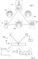
- Figure 10 illustrates the effect of height variation of the substrate.
- Figure 10(a) shows an oblique beam of illumination ILL incident on a target T on substrate S at angle ⁇ with respect to the substrate normal.
- Figure 10(a) shows this arrangement in a side-on view and top-down view.
- Figure 10(b) shows the same arrangement as that of Figure 10(a) , but where there has been a change in vertical position ⁇ Z of the target.
- this displacement ⁇ X the target will be measured by a different portion of the illumination spot.
- this illumination spot will typically have some inhomogeneity, there will be a resultant error in the Region of Interest (Rol) captured on the detector, where the RoI is the region of the captured target image used to determine the parameter of interest.
- RoI Region of Interest
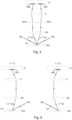
- Figure 11 illustrates the relationship between OPD and vertical position offset ⁇ Z .
- OPD is the additional distance travelled represented by L1+L2.
- the radiation diffracted by the target is the object beam that is imaged on the detector.
- OPD optical path difference
- ⁇ Z is the vertical position offset with respect to nominal
- phase term ⁇ s ( ⁇ ) represents a wavelength-dependent phase jump of the radiation diffracted by the grating. It can be shown that this term is responsible to a small process-dependent focus offset.
- the physics behind this is completely analogous to the process-dependency in a Level Sensor used for measuring a wafer height map in a lithography tool. More detail of this process-dependency is further described in a scientific paper: Jan van der Werf, J. Vac. Sci. Technol.
- F( ⁇ , ⁇ , P ) is a known function of wavelength ⁇ , illumination angle ⁇ and target grating pitch P :
- F ⁇ ⁇ P 1 cos ⁇ + 1 1 ⁇ ⁇ P ⁇ sin ⁇ 2
- phase parameter ⁇ 4 ⁇ Z 1 ⁇ ⁇ F ⁇ ⁇ ⁇ 1 ⁇ 2 F ⁇ + ⁇ ⁇ s ⁇ ⁇ ⁇
- a method for determining the vertical position offset from a multiple wavelength measurement.
- the method relies on detecting phase changes at a single point in the field as the wavelength is changed; i.e., effectively measuring the derivative d ⁇ / d ⁇ .
- This term is independent of grating position since the phase due to a grating shift X is given by 2 ⁇ X / P, which is independent of wavelength. This does assume that this position is sufficiently stable, however this is a requirement for a DHM in any case.
- each of a pair of complementary diffraction orders can be processed, as any phase variation in these orders due to a position change will have an opposite sign and therefore is distinguishable (and can be removed) from a determination of phase variation due to wavelength variation.
- the method may comprise obtaining at least one interference pattern on the detector using a metrology device, e.g., a holographic metrology device such as illustrated in Figure 8 , for each of a plurality of wavelengths.
- a first and second interference pattern may be recorded simultaneously for each wavelength, each pattern, per wavelength, corresponding to a measurement of a target or structure from a respective opposing direction.
- the interference pattern(s) may be processed to calculate a complex field of radiation at the detector ("complex" in this context meaning that both amplitude and phase information is present) associated with the scattered radiation (object beam).
- complex in this context meaning that both amplitude and phase information is present
- Such calculation of a complex field of radiation from an interference pattern formed by interfering reference radiation with radiation scattered from an object is known in general terms from holography. Further details about how to perform such calculations in the context of metrology for lithography may be found for example in US2016/0061750A1 , which is hereby incorporated by reference.
- the method in this embodiment may comprise fitting a sine function through the hologram image or complex field acquired by the detector.
- the concepts disclosed herein are not limited to holography metrology, and can be implemented using other metrology techniques (e.g., using a scatterometry based metrology device such as illustrated in Figure 9(a) ). All that is required is that the complex field of the measurement radiation be accessible. Other methods for accessing the complex field include phase-retrieval or shear interferometry. Phase-retrieval techniques in a lithography context are described for example, in US patent publication US2019/0107781 , which is incorporated herein by reference. These methods do not need a separate reference beam.
- the change in the phase difference between the object and reference beams ⁇ which results from a change in wavelength over a range ⁇ ⁇ can be determined.
- This change in the phase difference and wavelength step ⁇ ⁇ can then be put into the Equation for ⁇ Z given above, to determine the vertical position ⁇ Z with respect to nominal.
- level sensor or focus sensor for a holographic tool such as that illustrated in Figure 8 .
- level sensor would require no additional hardware, and the level sensing may be determined directly from the measurements performed
- the proposed method can be implemented without any hardware modification of the metrology tool, and without any additional metrology effort.
- FIG. 12 is a block diagram that illustrates a computer system 1500 that may assist in implementing the methods and flows disclosed herein.
- Computer system 1500 includes a bus 1502 or other communication mechanism for communicating information, and a processor 1504 (or multiple processors 1504 and 1505) coupled with bus 1502 for processing information.
- Computer system 1500 also includes a main memory 1506, such as a random access memory (RAM) or other dynamic storage device, coupled to bus 1502 for storing information and instructions to be executed by processor 1504.
- Main memory 1506 also may be used for storing temporary variables or other intermediate information during execution of instructions to be executed by processor 1504.
- Computer system 1500 further includes a read only memory (ROM) 1508 or other static storage device coupled to bus 1502 for storing static information and instructions for processor 1504.
- ROM read only memory
- a storage device 1510 such as a magnetic disk or optical disk, is provided and coupled to bus 1502 for storing information and instructions.
- Computer system 1500 may be coupled via bus 1502 to a display 1512, such as a cathode ray tube (CRT) or flat panel or touch panel display for displaying information to a computer user.
- a display 1512 such as a cathode ray tube (CRT) or flat panel or touch panel display for displaying information to a computer user.
- An input device 1514 is coupled to bus 1502 for communicating information and command selections to processor 1504.
- cursor control 1516 is Another type of user input device, cursor control 1516, such as a mouse, a trackball, or cursor direction keys for communicating direction information and command selections to processor 1504 and for controlling cursor movement on display 1512.
- This input device typically has two degrees of freedom in two axes, a first axis (e.g., x) and a second axis (e.g., y), that allows the device to specify positions in a plane.
- a touch panel (screen) display may also be used as an input device.
- One or more of the methods as described herein may be performed by computer system 1500 in response to processor 1504 executing one or more sequences of one or more instructions contained in main memory 1506. Such instructions may be read into main memory 1506 from another computer-readable medium, such as storage device 1510. Execution of the sequences of instructions contained in main memory 1506 causes processor 1504 to perform the process steps described herein. One or more processors in a multi-processing arrangement may also be employed to execute the sequences of instructions contained in main memory 1506. In an alternative embodiment, hard-wired circuitry may be used in place of or in combination with software instructions. Thus, the description herein is not limited to any specific combination of hardware circuitry and software.
- Non-volatile media include, for example, optical or magnetic disks, such as storage device 1510.
- Volatile media include dynamic memory, such as main memory 1506.
- Transmission media include coaxial cables, copper wire and fiber optics, including the wires that comprise bus 1502. Transmission media can also take the form of acoustic or light waves, such as those generated during radio frequency (RF) and infrared (IR) data communications.
- RF radio frequency
- IR infrared
- Computer-readable media include, for example, a floppy disk, a flexible disk, hard disk, magnetic tape, any other magnetic medium, a CD-ROM, DVD, any other optical medium, punch cards, paper tape, any other physical medium with patterns of holes, a RAM, a PROM, and EPROM, a FLASH-EPROM, any other memory chip or cartridge, a carrier wave as described hereinafter, or any other medium from which a computer can read.
- Various forms of computer readable media may be involved in carrying one or more sequences of one or more instructions to processor 1504 for execution.
- the instructions may initially be borne on a magnetic disk of a remote computer.
- the remote computer can load the instructions into its dynamic memory and send the instructions over a telephone line using a modem.
- a modem local to computer system 1500 can receive the data on the telephone line and use an infrared transmitter to convert the data to an infrared signal.
- An infrared detector coupled to bus 1502 can receive the data carried in the infrared signal and place the data on bus 1502.
- Bus 1502 carries the data to main memory 1506, from which processor 1504 retrieves and executes the instructions.
- the instructions received by main memory 1506 may optionally be stored on storage device 1510 either before or after execution by processor 1504.
- Computer system 1500 also preferably includes a communication interface 1518 coupled to bus 1502.
- Communication interface 1518 provides a two-way data communication coupling to a network link 1520 that is connected to a local network 1522.
- communication interface 1518 may be an integrated services digital network (ISDN) card or a modem to provide a data communication connection to a corresponding type of telephone line.
- ISDN integrated services digital network
- communication interface 1518 may be a local area network (LAN) card to provide a data communication connection to a compatible LAN.
- LAN local area network
- Wireless links may also be implemented.
- communication interface 1518 sends and receives electrical, electromagnetic or optical signals that carry digital data streams representing various types of information.
- Network link 1520 typically provides data communication through one or more networks to other data devices.
- network link 1520 may provide a connection through local network 1522 to a host computer 1524 or to data equipment operated by an Internet Service Provider (ISP) 1526.
- ISP 1526 in turn provides data communication services through the worldwide packet data communication network, now commonly referred to as the "Internet” 1528.
- Internet 1528 uses electrical, electromagnetic or optical signals that carry digital data streams.
- the signals through the various networks and the signals on network link 1520 and through communication interface 1518, which carry the digital data to and from computer system 1500, are exemplary forms of carrier waves transporting the information.
- Computer system 1500 may send messages and receive data, including program code, through the network(s), network link 1520, and communication interface 1518.
- a server 1530 might transmit a requested code for an application program through Internet 1528, ISP 1526, local network 1522 and communication interface 1518.
- One such downloaded application may provide for one or more of the techniques described herein, for example.
- the received code may be executed by processor 1504 as it is received, and/or stored in storage device 1510, or other non-volatile storage for later execution. In this manner, computer system 1500 may obtain application code in the form of a carrier wave.
- lithographic apparatus in the manufacture of ICs, it should be understood that the lithographic apparatus described herein may have other applications. Possible other applications include the manufacture of integrated optical systems, guidance and detection patterns for magnetic domain memories, flat-panel displays, liquid-crystal displays (LCDs), thin-film magnetic heads, etc.
- Embodiments of the invention may form part of a mask inspection apparatus, a metrology apparatus, or any apparatus that measures or processes an object such as a wafer (or other substrate) or mask (or other patterning device). These apparatus may be generally referred to as lithographic tools. Such a lithographic tool may use vacuum conditions or ambient (non-vacuum) conditions.
Priority Applications (3)
| Application Number | Priority Date | Filing Date | Title |
|---|---|---|---|
| EP22163109.6A EP4246231A1 (de) | 2022-03-18 | 2022-03-18 | Verfahren zur bestimmung einer vertikalen position einer struktur auf einem substrat und zugehörige vorrichtungen |
| PCT/EP2023/054365 WO2023174650A1 (en) | 2022-03-18 | 2023-02-22 | A method for determining a vertical position of a structure on a substrate and associated apparatuses |
| TW112109892A TW202401164A (zh) | 2022-03-18 | 2023-03-17 | 用於判定一基板上之一結構之一垂直位置之方法及相關聯設備 |
Applications Claiming Priority (1)
| Application Number | Priority Date | Filing Date | Title |
|---|---|---|---|
| EP22163109.6A EP4246231A1 (de) | 2022-03-18 | 2022-03-18 | Verfahren zur bestimmung einer vertikalen position einer struktur auf einem substrat und zugehörige vorrichtungen |
Publications (1)
| Publication Number | Publication Date |
|---|---|
| EP4246231A1 true EP4246231A1 (de) | 2023-09-20 |
Family
ID=80820296
Family Applications (1)
| Application Number | Title | Priority Date | Filing Date |
|---|---|---|---|
| EP22163109.6A Pending EP4246231A1 (de) | 2022-03-18 | 2022-03-18 | Verfahren zur bestimmung einer vertikalen position einer struktur auf einem substrat und zugehörige vorrichtungen |
Country Status (3)
| Country | Link |
|---|---|
| EP (1) | EP4246231A1 (de) |
| TW (1) | TW202401164A (de) |
| WO (1) | WO2023174650A1 (de) |
Citations (26)
| Publication number | Priority date | Publication date | Assignee | Title |
|---|---|---|---|---|
| US5880838A (en) * | 1996-06-05 | 1999-03-09 | California Institute Of California | System and method for optically measuring a structure |
| US6952253B2 (en) | 2002-11-12 | 2005-10-04 | Asml Netherlands B.V. | Lithographic apparatus and device manufacturing method |
| US20060033921A1 (en) | 2004-08-16 | 2006-02-16 | Asml Netherlands B.V. | Method and apparatus for angular-resolved spectroscopic lithography characterization |
| US20090109438A1 (en) * | 2007-10-24 | 2009-04-30 | Dainippon Screen Mfg. Co., Ltd. | Spectroscopic ellipsometer and ellipsometry |
| WO2009078708A1 (en) | 2007-12-17 | 2009-06-25 | Asml Netherlands B.V. | Diffraction based overlay metrology tool and method |
| WO2009106279A1 (en) | 2008-02-29 | 2009-09-03 | Asml Netherlands B.V. | Metrology method and apparatus, lithographic apparatus, and device manufacturing method |
| US20100201963A1 (en) | 2009-02-11 | 2010-08-12 | Asml Netherlands B.V. | Inspection Apparatus, Lithographic Apparatus, Lithographic Processing Cell and Inspection Method |
| US20110026032A1 (en) | 2008-04-09 | 2011-02-03 | Asml Netherland B.V. | Method of Assessing a Model of a Substrate, an Inspection Apparatus and a Lithographic Apparatus |
| US20110027704A1 (en) | 2009-07-31 | 2011-02-03 | Asml Netherlands B.V. | Methods and Scatterometers, Lithographic Systems, and Lithographic Processing Cells |
| US20110032500A1 (en) * | 2008-03-20 | 2011-02-10 | Asml Netherlands B.V. | Inspection apparatus for lithography |
| US20110043791A1 (en) | 2009-08-24 | 2011-02-24 | Asml Netherlands B.V. | Metrology Method and Apparatus, Lithographic Apparatus, Device Manufacturing Method and Substrate |
| US20110102753A1 (en) | 2008-04-21 | 2011-05-05 | Asml Netherlands B.V. | Apparatus and Method of Measuring a Property of a Substrate |
| US20110249244A1 (en) | 2008-10-06 | 2011-10-13 | Asml Netherlands B.V. | Lithographic Focus and Dose Measurement Using A 2-D Target |
| US20120044470A1 (en) | 2010-08-18 | 2012-02-23 | Asml Netherlands B.V. | Substrate for Use in Metrology, Metrology Method and Device Manufacturing Method |
| US20120123581A1 (en) | 2010-11-12 | 2012-05-17 | Asml Netherlands B.V. | Metrology Method and Inspection Apparatus, Lithographic System and Device Manufacturing Method |
| US20130258310A1 (en) | 2012-03-27 | 2013-10-03 | Asml Netherlands B.V. | Metrology Method and Apparatus, Lithographic System and Device Manufacturing Method |
| US20130271740A1 (en) | 2012-04-16 | 2013-10-17 | Asml Netherlands B.V. | Lithographic Apparatus, Substrate and Device Manufacturing Method |
| WO2013178422A1 (en) | 2012-05-29 | 2013-12-05 | Asml Netherlands B.V. | Metrology method and apparatus, substrate, lithographic system and device manufacturing method |
| US20160061750A1 (en) | 2014-08-28 | 2016-03-03 | Vrije Universiteit Amsterdam | Inspection Apparatus, Inspection Method And Manufacturing Method |
| US20160161863A1 (en) | 2014-11-26 | 2016-06-09 | Asml Netherlands B.V. | Metrology method, computer product and system |
| US20160161864A1 (en) | 2013-08-07 | 2016-06-09 | Asml Netherlands B.V. | Metrology Method and Apparatus, Lithographic System and Device Manufacturing Method |
| US20160370717A1 (en) | 2015-06-17 | 2016-12-22 | Asml Netherlands B.V. | Recipe selection based on inter-recipe consistency |
| US20190107781A1 (en) | 2017-10-05 | 2019-04-11 | Stichting Vu | Metrology System and Method For Determining a Characteristic of One or More Structures on a Substrate |
| WO2019197117A1 (en) | 2018-04-09 | 2019-10-17 | Stichting Vu | Method of determining a characteristic of a structure, and metrology apparatus |
| US20200174425A1 (en) * | 2015-08-06 | 2020-06-04 | Centauri, Llc | Systems and methods for simultaneous multi-channel off-axis holography |
| WO2021121733A1 (en) | 2019-12-17 | 2021-06-24 | Asml Netherlands B.V. | Dark field digital holographic microscope and associated metrology method |
Family Cites Families (1)
| Publication number | Priority date | Publication date | Assignee | Title |
|---|---|---|---|---|
| US668506A (en) | 1900-10-24 | 1901-02-19 | Henry M Enright | Tracer. |
-
2022
- 2022-03-18 EP EP22163109.6A patent/EP4246231A1/de active Pending
-
2023
- 2023-02-22 WO PCT/EP2023/054365 patent/WO2023174650A1/en unknown
- 2023-03-17 TW TW112109892A patent/TW202401164A/zh unknown
Patent Citations (29)
| Publication number | Priority date | Publication date | Assignee | Title |
|---|---|---|---|---|
| US5880838A (en) * | 1996-06-05 | 1999-03-09 | California Institute Of California | System and method for optically measuring a structure |
| US6952253B2 (en) | 2002-11-12 | 2005-10-04 | Asml Netherlands B.V. | Lithographic apparatus and device manufacturing method |
| US20060033921A1 (en) | 2004-08-16 | 2006-02-16 | Asml Netherlands B.V. | Method and apparatus for angular-resolved spectroscopic lithography characterization |
| EP1628164A2 (de) | 2004-08-16 | 2006-02-22 | ASML Netherlands B.V. | Verfahren und Vorrichtung zur Charakterisierung der Lithographie mittels winkelaufgelöster Spektroskopie |
| US20060066855A1 (en) | 2004-08-16 | 2006-03-30 | Asml Netherlands B.V. | Method and apparatus for angular-resolved spectroscopic lithography characterization |
| US20090109438A1 (en) * | 2007-10-24 | 2009-04-30 | Dainippon Screen Mfg. Co., Ltd. | Spectroscopic ellipsometer and ellipsometry |
| WO2009078708A1 (en) | 2007-12-17 | 2009-06-25 | Asml Netherlands B.V. | Diffraction based overlay metrology tool and method |
| US20100328655A1 (en) | 2007-12-17 | 2010-12-30 | Asml, Netherlands B.V. | Diffraction Based Overlay Metrology Tool and Method |
| WO2009106279A1 (en) | 2008-02-29 | 2009-09-03 | Asml Netherlands B.V. | Metrology method and apparatus, lithographic apparatus, and device manufacturing method |
| US20110032500A1 (en) * | 2008-03-20 | 2011-02-10 | Asml Netherlands B.V. | Inspection apparatus for lithography |
| US20110026032A1 (en) | 2008-04-09 | 2011-02-03 | Asml Netherland B.V. | Method of Assessing a Model of a Substrate, an Inspection Apparatus and a Lithographic Apparatus |
| US20110102753A1 (en) | 2008-04-21 | 2011-05-05 | Asml Netherlands B.V. | Apparatus and Method of Measuring a Property of a Substrate |
| US20110249244A1 (en) | 2008-10-06 | 2011-10-13 | Asml Netherlands B.V. | Lithographic Focus and Dose Measurement Using A 2-D Target |
| US20100201963A1 (en) | 2009-02-11 | 2010-08-12 | Asml Netherlands B.V. | Inspection Apparatus, Lithographic Apparatus, Lithographic Processing Cell and Inspection Method |
| US20110027704A1 (en) | 2009-07-31 | 2011-02-03 | Asml Netherlands B.V. | Methods and Scatterometers, Lithographic Systems, and Lithographic Processing Cells |
| US20110043791A1 (en) | 2009-08-24 | 2011-02-24 | Asml Netherlands B.V. | Metrology Method and Apparatus, Lithographic Apparatus, Device Manufacturing Method and Substrate |
| US20120044470A1 (en) | 2010-08-18 | 2012-02-23 | Asml Netherlands B.V. | Substrate for Use in Metrology, Metrology Method and Device Manufacturing Method |
| US20120123581A1 (en) | 2010-11-12 | 2012-05-17 | Asml Netherlands B.V. | Metrology Method and Inspection Apparatus, Lithographic System and Device Manufacturing Method |
| US20130258310A1 (en) | 2012-03-27 | 2013-10-03 | Asml Netherlands B.V. | Metrology Method and Apparatus, Lithographic System and Device Manufacturing Method |
| US20130271740A1 (en) | 2012-04-16 | 2013-10-17 | Asml Netherlands B.V. | Lithographic Apparatus, Substrate and Device Manufacturing Method |
| WO2013178422A1 (en) | 2012-05-29 | 2013-12-05 | Asml Netherlands B.V. | Metrology method and apparatus, substrate, lithographic system and device manufacturing method |
| US20160161864A1 (en) | 2013-08-07 | 2016-06-09 | Asml Netherlands B.V. | Metrology Method and Apparatus, Lithographic System and Device Manufacturing Method |
| US20160061750A1 (en) | 2014-08-28 | 2016-03-03 | Vrije Universiteit Amsterdam | Inspection Apparatus, Inspection Method And Manufacturing Method |
| US20160161863A1 (en) | 2014-11-26 | 2016-06-09 | Asml Netherlands B.V. | Metrology method, computer product and system |
| US20160370717A1 (en) | 2015-06-17 | 2016-12-22 | Asml Netherlands B.V. | Recipe selection based on inter-recipe consistency |
| US20200174425A1 (en) * | 2015-08-06 | 2020-06-04 | Centauri, Llc | Systems and methods for simultaneous multi-channel off-axis holography |
| US20190107781A1 (en) | 2017-10-05 | 2019-04-11 | Stichting Vu | Metrology System and Method For Determining a Characteristic of One or More Structures on a Substrate |
| WO2019197117A1 (en) | 2018-04-09 | 2019-10-17 | Stichting Vu | Method of determining a characteristic of a structure, and metrology apparatus |
| WO2021121733A1 (en) | 2019-12-17 | 2021-06-24 | Asml Netherlands B.V. | Dark field digital holographic microscope and associated metrology method |
Also Published As
| Publication number | Publication date |
|---|---|
| TW202401164A (zh) | 2024-01-01 |
| WO2023174650A1 (en) | 2023-09-21 |
Similar Documents
| Publication | Publication Date | Title |
|---|---|---|
| US20230044632A1 (en) | Dark field digital holographic microscope and associated metrology method | |
| NL2017949A (en) | Metrology method, target and substrate | |
| US11709436B2 (en) | Metrology apparatus and method for determining a characteristic of one or more structures on a substrate | |
| US11181828B2 (en) | Method of determining a value of a parameter of interest of a patterning process, device manufacturing method | |
| EP3531191A1 (de) | Metrologievorrichtung und verfahren zum bestimmen einer eigenschaft einer oder mehrerer strukturen auf einem substrat | |
| TWI696894B (zh) | 評估圖案化製程之方法與系統及相關之非暫時性電腦程式產品 | |
| US20220350260A1 (en) | A method for filtering an image and associated metrology apparatus | |
| US20190214318A1 (en) | Method and apparatus to monitor a process apparatus | |
| EP3605230A1 (de) | Metrologievorrichtung und verfahren zur bestimmung einer eigenschaft einer oder mehrerer strukturen auf einem substrat | |
| EP3839635A1 (de) | Digitales holographisches dunkelfeldmikroskop und zugehöriges messverfahren | |
| EP4246231A1 (de) | Verfahren zur bestimmung einer vertikalen position einer struktur auf einem substrat und zugehörige vorrichtungen | |
| CN116569111A (zh) | 量测方法和相关联的设备 | |
| CN111095112B (zh) | 光刻过程中的量测 | |
| NL2024478A (en) | Dark field digital holographic microscope and associated metrology method | |
| EP4312079A1 (de) | Verfahren zum vermindern des übersprechens in metrologischen bildern | |
| EP4318131A1 (de) | Sensormodul, beleuchtungsvorrichtung, metrologievorrichtung und zugehöriges metrologieverfahren | |
| EP4080284A1 (de) | Metrologiewerkzeugkalibrierungsverfahren und zugehöriges metrologiewerkzeug | |
| EP4246232A1 (de) | Beleuchtungsanordnung für eine metrologievorrichtung und zugehöriges verfahren | |
| EP4332678A1 (de) | Holographisches lithographiegerät und verfahren | |
| EP4124909A1 (de) | Verfahren und vorrichtung für die metrologie | |
| TWI828087B (zh) | 校正全像影像之方法及相關的處理器件及相關程式儲存器、暗場數位全像顯微鏡、度量衡裝置、及檢測裝置 | |
| EP4063971A1 (de) | Digitales holografisches mikroskop und zugehöriges metrologieverfahren | |
| EP4187321A1 (de) | Metrologisches verfahren und zugehöriges metrologisches werkzeug | |
| EP4339703A1 (de) | Metrologieverfahren und zugehörige metrologievorrichtung | |
| WO2022263231A1 (en) | Metrology method and device |
Legal Events
| Date | Code | Title | Description |
|---|---|---|---|
| PUAI | Public reference made under article 153(3) epc to a published international application that has entered the european phase |
Free format text: ORIGINAL CODE: 0009012 |
|
| STAA | Information on the status of an ep patent application or granted ep patent |
Free format text: STATUS: THE APPLICATION HAS BEEN PUBLISHED |
|
| AK | Designated contracting states |
Kind code of ref document: A1 Designated state(s): AL AT BE BG CH CY CZ DE DK EE ES FI FR GB GR HR HU IE IS IT LI LT LU LV MC MK MT NL NO PL PT RO RS SE SI SK SM TR |